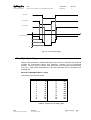
1
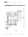
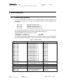
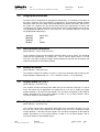
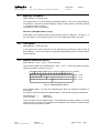
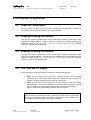
Technical
Information
Manual
Revision n. 3
6 September 2002
NPO:
00101/97:V814x.MUTx/03
MOD. V 814 series
16 CHANNEL
LOW THRESHOLD
DISCRIMINATORS
CAEN will repair or replace any product within the guarantee period if the Guarantor declares
that the product is defective due to workmanship or materials and has not been caused by
mishandling, negligence on behalf of the User, accident or any abnormal conditions or
operations.
CAEN declines all responsibility for damages or
injuries caused by an improper use of the Modules due
to negligence on behalf of the User. It is strongly
recommended to read thoroughly the CAEN User's
Manual before any kind of operation.
CAEN reserves the right to change partially or entirely the contents of this Manual at any time and
without giving any notice.
Document type:
User's Manual (MUT)
Title:
Mod. V814 16 Channel Low Threshold Discriminator
Revision date:
06/09/2002
Revision:
3
TABLE OF CONTENTS
1.
GENERAL DESCRIPTION.................................................................................................................. 5
1.1.
FUNCTIONAL DESCRIPTION ...................................................................................................................... 5
1.2.
BLOCK DIAGRAM ..................................................................................................................................... 7
1.3.
TECHNICAL SPECIFICATION TABLE........................................................................................................... 8
2.
TECHNICAL SPECIFICATIONS ....................................................................................................... 9
2.1.
PACKAGING ............................................................................................................................................. 9
2.2.
POWER REQUIREMENTS ........................................................................................................................... 9
2.3.
FRONT PANEL ........................................................................................................................................ 10
2.4. EXTERNAL CONNECTORS EXTERNAL CONNECTORS ............................................................................... 11
2.4.1.
INPUT connectors ........................................................................................................................ 11
2.4.2.
OUTPUT connectors .................................................................................................................... 11
2.5. OTHER COMPONENTS ............................................................................................................................. 12
2.5.1.
Displays ........................................................................................................................................ 12
2.5.2.
Switches ........................................................................................................................................ 12
2.5.3.
Jumpers......................................................................................................................................... 12
3.
VME INTERFACE .............................................................................................................................. 15
3.1.
ADDRESSING CAPABILITY ...................................................................................................................... 15
3.2.
GEOGRAPHICAL ADDRESS ...................................................................................................................... 16
3.3.
DISCRIMINATOR THRESHOLD ................................................................................................................. 16
3.4.
PATTERN OF INHIBIT .............................................................................................................................. 16
3.5.
OUTPUT WIDTH CH. 0 TO 7 .................................................................................................................... 16
3.6.
OUTPUT WIDTH CH. 8 TO 15 .................................................................................................................. 16
3.7.
MAJORITY THRESHOLD .......................................................................................................................... 17
3.8.
TEST PULSE ............................................................................................................................................ 17
3.9.
MODULE IDENTIFIER WORDS ................................................................................................................. 17
4.
PRINCIPLES OF OPERATION ........................................................................................................ 18
4.1.
POWER ON / RESET STATUS .................................................................................................................. 18
4.2.
ENABLING/DISABLING THE CHANNELS .................................................................................................. 18
4.3.
ENABLING/DISABLING THE CHANNELS .................................................................................................. 18
4.4.
TEST, VETO AND OR SIGNALS ............................................................................................................... 18
4.5.
CHANNELS TEST .................................................................................................................................... 19
4.6.
SETTING THE THRESHOLD ...................................................................................................................... 19
NPO:
00101/97:V814x.MUTx/03
Filename:
V814_REV3.DOC
Number of pages:
22
Page:
3
Document type:
User's Manual (MUT)
Title:
Mod. V814 16 Channel Low Threshold Discriminator
Revision date:
06/09/2002
Revision:
3
4.7.
SETTING THE OUTPUT PULSE WIDTH ...................................................................................................... 19
4.8.
CURRENT SUM SIGNAL .......................................................................................................................... 19
4.9.
MAJORITY SETTING................................................................................................................................ 20
LIST OF FIGURES
FIG. 1.1: MODEL TYPE LABEL (EXAMPLE) ............................................................................................................... 6
FIG. 1.2: BLOCK DIAGRAM ...................................................................................................................................... 7
FIG. 2.1: MOD. V 814 FRONT PANEL ..................................................................................................................... 10
FIG. 2.2: COMPONENTS LOCATION......................................................................................................................... 13
FIG. 2.3: JUMPERS LOCATION ................................................................................................................................ 14
FIG. 3.1: MODULE IDENTIFIER WORDS .................................................................................................................. 17
FIG. 4.1: CURRENT SUM SIGNAL............................................................................................................................ 20
FIG. 4.2: EXAMPLE OF THREE DAISY CHAINED V814 ............................................................................................. 22
LIST OF TABLES
TABLE 1.1:VERSIONS AVAILABLE FOR THE MODEL V814 ....................................................................................... 6
TABLE 1.2: TECHNICAL SPECIFICATION TABLE ........................................................................................................ 8
TABLE 2.1: POWER REQUIREMENTS ......................................................................................................................... 9
TABLE 3.1: ADDRESS MAP .................................................................................................................................... 15
TABLE 4.1: MAJORITY LEVEL SETTING VALUES .................................................................................................... 20
NPO:
00101/97:V814x.MUTx/03
Filename:
V814_REV3.DOC
Number of pages:
22
Page:
4
Document type:
User's Manual (MUT)
Title:
Mod. V814 16 Channel Low Threshold Discriminator
Revision date:
06/09/2002
Revision:
3
1. General description
1.1.
Functional description
The CAEN Model V814 is a 16 CHANNEL LOW THRESHOLD DISCRIMINATOR housed
in a single width VME module. The module accepts 16 (either negative or positive) inputs
and produces 16 differential ECL outputs with a fan-out of two on four front panel flat
cable connectors (a functional block diagram is shown in Fig. 1.2).
Input and output stages are independently organized for each channel. Each channel can
be turned on or off via VME by using a mask register (Pattern of Inhibit). The timing stage
of the discriminator produces an output pulse whose width is adjustable in a range from 6
to 95 ns via VME.
The discriminator thresholds are individually settable in a range from -1 mV to -255 mV
(1 mV step), via VME through an 8-bit DAC, a positive input version (Model V814 P), with the
thresholds settable in the 1 mV to 255 mV range, is also available.
VETO and TEST inputs are available on the front panel.
On the front panel a Current Sum output is also available that generates a current
proportional to the input multiplicity, i. e. to the number of channels over threshold, at a
rate of -1.0 mA per hit (-50 mV per hit into a 50 Ohm load) ±20 %.
A “MAJORITY” output connector provides a NIM signal if the number of input channels
over threshold exceeds the MAJORITY programmed value.
The logic OR of discriminator output is available on a front panel connector. The relevant
“OR” LED lights up if at least one of the unmasked channels is over threshold.
The module’s operations are completely controlled via software for each channel through
the VME bus. The most important are:
• setting the discriminator thresholds (8 bit) from -1 to -255 mV (V814 P: 1÷255 mV).
• setting Pattern of Inhibit; each channel can be turned “ON” or “OFF” by using a mask
register.
• setting output width in a range from 6 to 95 ns.
• setting the Majority threshold value.
• common TEST
Several versions of the module are available, please refer to Table 1.1 for details.
NPO:
00101/97:V814x.MUTx/03
Filename:
V814_REV3.DOC
Number of pages:
22
Page:
5
Document type:
User's Manual (MUT)
Title:
Mod. V814 16 Channel Low Threshold Discriminator
Revision date:
06/09/2002
Revision:
3
Table 1.1:Versions available for the Model V814
1
Number of
channels
PAUX
2
connector
Input type
16
yes
Negative
V814 P
16
yes
Positive
V814 B
16
no
Negative
V814 PB
16
no
Positive
Version
V814
3
3
TYPE
RIF N.
DATE
WV814XBAAAAA
MAY 5th 2002
Fig. 1.1: Model type label (example: V814 B)
1
A label on the printed board soldering side indicates the module’s version (see Fig 1.1); all the
versions share the same features except where indicated.
2
The version with the PAUX connector requires the V430 backplane.
3
Models available exclusively on request.
NPO:
00101/97:V814x.MUTx/03
Filename:
V814_REV3.DOC
Number of pages:
22
Page:
6
Document type:
User's Manual (MUT)
Title:
Mod. V814 16 Channel Low Threshold Discriminator
Revision date:
06/09/2002
Revision:
3
1.2. Block diagram
DACs,TEST,
INHIBIT
W LOGIC
........................
8 bit
DAC
DAC
8 bit
8 bit
..................
DAC
DAC
DAC
MAJ
ch.0
ch.1
ch.15
ch14
8 bit
inhibit
THRESHOLDS
TEST AND
WIDTH
VME
INTERFACE
VME
BUS
8 bit
test
INPUTS<0..15>
MAJ
Σ
discr.
discr. ................. discr.
discr.
ch.0
ch.1
ch.15
ch.14
TEST
VETO
OUTPUTS<0..15> A, B
OR OUT
OR LED
Fig. 1.2: Block Diagram
NPO:
00101/97:V814x.MUTx/03
Filename:
V814_REV3.DOC
Number of pages:
22
Page:
7
Document type:
User's Manual (MUT)
Title:
Mod. V814 16 Channel Low Threshold Discriminator
Revision date:
06/09/2002
Revision:
3
1.3. Technical specification table
Table 1.2: Technical specification table
Packaging
6U-high, 1U-wide VME unit
Power requirements
Refer to § 2.2
Inputs
16 inputs (50 Ω impedance, DC coupling)
Input voltage range
V814/V814B: -1 mV to -400 mV; V814 P/PB: 1 mV to 400 mV
Max input frequency
60 MHz (8 ns output pulse width)
Double pulse resolution
16 ns (8 ns output pulse width)
Threshold range
V814/V814B: -1 ÷ -255 mV; V814 P/PB: 1 ÷ 255 mV (1 mV step)
Outputs
16 outputs with a fan-out of two (ECL, 110 Ω impedance)
Input/output delay
10.5±1.5 ns
Output width
Programmable from 6±1 ns to 95±7 ns
Interchannel insulation
54 dB for 2.5 ns rise time input signals
Control inputs
NIM logic signals, high impedance:
VETO: allows vetoing of all channels simultaneously
TEST: triggers all the enabled channels at once
Control outputs
Displays
NPO:
00101/97:V814x.MUTx/03
MAJORITY: standard NIM logic signal, 50 Ω impedance; it
indicates if the number of input channels over threshold exceeds
the MAJORITY level programmed via VME
OR: standard NIM signal, 50 Ω impedance; logic OR of outputs
Σ: current proportional to input multiplicity (-1 mA ± 20% per hit),
high impedance
DTACK: green LED; lights up at each VME access
OR: green LED; it lights up if at least one output signal is present
Filename:
V814_REV3.DOC
Number of pages:
22
Page:
8
Document type:
User's Manual (MUT)
Title:
Mod. V814 16 Channel Low Threshold Discriminator
Revision date:
06/09/2002
Revision:
3
2. Technical Specifications
2.1.
Packaging
The modules are housed in 6U-high 1U-wide VME units.
The Mod. V814/V814 P is provided with P1, P2 and PAUX connectors.
The Mod. V814 B/V814 PB is provided with P1, P2 connectors (NO PAUX).
2.2.
Power requirements
The power requirements of the various versions are as follows:
Table 2.1: Power requirements
Power supply
V814/V814 P
+ 12 V
- 12 V
+5V
- 5V
NPO:
00101/97:V814x.MUTx/03
100 mA
50 mA
800 mA
3.3 A
Filename:
V814_REV3.DOC
V814 B/V814 PB
(no PAUX)
100 mA
50 mA
5.1 A
-
Number of pages:
22
Page:
9
Document type:
User's Manual (MUT)
Title:
Mod. V814 16 Channel Low Threshold Discriminator
Revision date:
06/09/2002
Revision:
3
2.3. Front Panel
Mod. V814
14
15
I
N
12
13
10
11
8
9
- +
- +
15
8
OUT
T
E
S
T
OR
DTK
MAJ
V
E
T
O
Σ
- +
- +
7
0
OUT
6
7
4
2
5
I
N
0
3
1
16 CH
CH
16
LTD
Fig. 2.1: Mod. V 814 front panel
NPO:
00101/97:V814x.MUTx/03
Filename:
V814_REV3.DOC
Number of pages:
22
Page:
10
Document type:
User's Manual (MUT)
Title:
Mod. V814 16 Channel Low Threshold Discriminator
Revision date:
06/09/2002
Revision:
3
2.4. External connectors External connectors
The location of the connectors is shown in Fig. 2.1. Their function and electromechanical
specifications are listed in the following subsections.
2.4.1. INPUT connectors
INPUT CHANNELS:
Mechanical specifications:
16 LEMO 00 type connectors.
Electrical specifications:
negative polarity, 50 Ohm impedance, DC
coupling; ratings: V814: -1÷-400 mV; V814 P:
1÷400 mV; 60 MHz maximum input
frequency.
VETO INPUT:
Mechanical specifications:
1 LEMO 00 type connectors.
Electrical specifications:
standard NIM logic signal, high impedance,
20 ns minimum FWHM; leading edge of the
VETO signal must precede of at least 8 ns the
leading edge of the input and overlap
completely the input signal; acts on all
signals.
TEST INPUT:
Mechanical specifications:
1 LEMO 00 type connectors.
Electrical specifications:
standard NIM logic signal, high impedance,
5 ns minimum FWHM, 60 MHz maximum
input frequency.
2.4.2. OUTPUT connectors
OUTPUT CHANNELS:
Mechanical specifications:
4 Header 3M 3408-D202 type, 8+8 pin
connectors.
Electrical specifications:
Differential ECL level on 110 Ohm
impedance; pulse width adjustment from
6±1 ns to 95±7 ns.
Input/Output delay: 10.5±1.5 ns.
OR OUTPUT:
Mechanical specifications:
1 LEMO 00 type connectors.
Electrical specifications:
standard NIM logic signal, 50 Ω impedance.
NPO:
00101/97:V814x.MUTx/03
Filename:
V814_REV3.DOC
Number of pages:
22
Page:
11
Document type:
User's Manual (MUT)
Title:
Mod. V814 16 Channel Low Threshold Discriminator
Revision date:
06/09/2002
Revision:
3
Σ OUTPUT:
Mechanical specifications:
1 LEMO 00 type connectors.
Electrical specifications:
current output (-1 mA ± 20% per hit), high
impedance.
MAJORITY OUTPUT:
Mechanical specifications:
1 LEMO 00 type connectors.
Electrical specifications:
standard NIM logic signal, 50 Ω impedance.
2.5. Other components
2.5.1. Displays
The front panel hosts the following LEDs:
DTACK
Type: 1 green LED
Function: VME selected; it lights up during a VME access.
OR
Type: 1 green LED
Function: it lights up if at least one output signal is present.
2.5.2. Switches
ROTARY SWITCHES
Function: they allow to select module’s VME address; please refer to Fig. 2.2 for their
setting.
2.5.3. Jumpers
JP1
Function: it allows to select the Majority logic (Internal, External); please refer to Fig. 2.3
for the jumper location on the V814 board.
NPO:
00101/97:V814x.MUTx/03
Filename:
V814_REV3.DOC
Number of pages:
22
Page:
12
Title:
Mod. V814 16 Channel Low Threshold Discriminator
0 1
BC D
A
45
Base address bit <23 ... 20>
8 9
A
45
67
8 9
Channels 8 to 14
R otary switches for
Base Address selection
0 1
BC D
E
F
23
Base address bit <19 ... 16>
Revision:
3
23
F
E
Revision date:
06/09/2002
67
Document type:
User's Manual (MUT)
Discrim inator
Ch. 14 - Ch. 15
VM E P1
connector
Discrim inator
Ch. 12 - Ch. 13
Flat Cable
C onnectors A-B
Discrim inator
Ch. 10 - Ch. 11
OR
Rotary switches for
Base Address selection
Discrim inator
Ch. 8 - Ch. 9
Test
MAJ
Veto
SUM
Discrim inator
Ch. 6 - Ch. 7
VM E PAUX connector
Discrim inator
Ch. 4 - Ch. 5
Flat Cable
Connectors A-B
VME P2
connector
Discrim inator
Ch. 2 - Ch. 3
Channels 0 to 7
Discrim inator
Ch. 0 - Ch. 1
C omponent side of the board
0 1
8 9
BC D
0 1
Rotary switches for
Base Address selection
A
45
Base address bit <27 ... 24>
F
23
E
67
Base address bit <31 ... 28>
67
A
45
BC D
F
23
E
8 9
Fig. 2.2: Components location
NPO:
00101/97:V814x.MUTx/03
Filename:
V814_REV3.DOC
Number of pages:
22
Page:
13
Document type:
User's Manual (MUT)
Title:
Mod. V814 16 Channel Low Threshold Discriminator
Revision date:
06/09/2002
Revision:
3
VME P1
connector
Internal
JP1
External
VME PAUX connector
VME P2
connector
Com ponents side
Fig. 2.3: Jumpers location
NPO:
00101/97:V814x.MUTx/03
Filename:
V814_REV3.DOC
Number of pages:
22
Page:
14
Document type:
User's Manual (MUT)
Title:
Mod. V814 16 Channel Low Threshold Discriminator
Revision date:
06/09/2002
Revision:
3
3. VME Interface
3.1. Addressing capability
The V814 module works in A24/A32 mode. This implies that the module’s address must
be specified in a field of 24 or 32 bits. The address modifiers codes recognized by the
module are:
AM = %39
AM = %3D
AM = %09
AM = %0D
Standard user data access
Standard supervisor data access
Extended user data access
Extended supervisor data access
The module’s Base address is fixed by 4 Internal rotary switches housed on two piggyback boards plugged into the main printed circuit board (see Fig. 2.2).
The Base address can be selected in the range:
% 00 0000 <-> % FF 0000
A24 mode
% 0000 0000 <-> % FFFF 0000
A32 mode
The module’s address lines A09÷A15 are not connected, so their content is meaningless:
for example writing to either Base + 104C or Base + 284C the same register is accessed.
Table 3.1: Address Map
ADDRESS
Base + %00
Base + %02
Base + %04
Base + %06
Base + %08
Base + %0A
Base + %0C
Base + %0E
Base + %10
Base + %12
Base + %14
Base + %16
Base + %18
Base + %1A
Base + %1C
Base + %1E
Base + %40
Base + %42
Base + %48
Base + %4A
Base + %4C
Base + %FA
Base + %FC
Base + %FE
NPO:
00101/97:V814x.MUTx/03
REGISTER/CONTEN T
Threshold register Ch. 0
Threshold register Ch. 1
Threshold register Ch. 2
Threshold register Ch. 3
Threshold register Ch. 4
Threshold register Ch. 5
Threshold register Ch. 6
Threshold register Ch. 7
Threshold register Ch. 8
Threshold register Ch. 9
Threshold register Ch. 10
Threshold register Ch. 11
Threshold register Ch. 12
Threshold register Ch. 13
Threshold register Ch. 14
Threshold register Ch. 15
Output width register Ch. 0 to 7
Output width register Ch. 8 to 15
Majority threshold register
Pattern Inhibit register
Test pulse register
Fixed code
Manufacturer & Module type
Version & Serial number
Filename:
V814_REV3.DOC
TYPE
Write only
Write only
Write only
Write only
Write only
Write only
Write only
Write only
Write only
Write only
Write only
Write only
Write only
Write only
Write only
Write only
Write only
Write only
Write only
Write only
Write only
Read only
Read only
Read only
Number of pages:
22
Page:
15
Document type:
User's Manual (MUT)
Title:
Mod. V814 16 Channel Low Threshold Discriminator
Revision date:
06/09/2002
Revision:
3
3.2. Geographical address
The board can be addressed via geographical addressing (i.e. according to its position in
the crate, neglecting the rotary switches configuration), by specifying address modifier
AM=0x2F. Each slot of the VME crate is identified by the status of the SN5...SN1 lines of
the JAUX: for example, the slot #5 will have these lines respectively at 00101 and
consequently the module inserted in the slot #5 will have a GEO address set to 00101.
The geographical address works in A24 mode only. The complete address in A24 mode
for geographical addressing is:
A[31:24]
A[23:19]
A[18:16]
A[15:0]
don't care
GEO
0
offset
3.3. Discriminator threshold
(Base address + %00 to %1E write only)
These registers contain the discriminator threshold values on 8 bit words. The threshold
values can be programmed in a range from -1 mV to -255 mV (Mod. V814 P: 1 to 255
mV) with 1 mV steps, writing an integer number between 0 and 255 into the register; the
channel thresholds are individually settable.
3.4. Pattern of Inhibit
(Base address + %4A write only)
This register contains the Pattern of Inhibit, a 16 bit word indicating which channels are
either enabled or disabled (bit X=1 ⇒ Ch. X enabled…bitX=0 ⇒ Ch. X disabled).
3.5. Output width Ch. 0 to 7
(Base address + %40 write only)
This register contains the output pulse width value of the channels 0 through 7 on a 8 bit
word. This value can be adjusted in the range from 6 ns to 95 ns, writing an integer
number between 0 and 255 into the register. The set value corresponds to the width as
follows: 255 leads to a 95 ns pulse duration, 0 leads to a 6 ns pulse duration, with a
non-linear relation for intermediate values.
3.6. Output width Ch. 8 to 15
(Base address + %42 write only)
This register contains the output pulse width value of the channels 8 through 15 on a 8
bit word. This value can be adjusted in the range from 6 ns to 95 ns, writing an integer
number between 0 and 255 into the register. The set value corresponds to the width as
follows: 255 leads to a 95 ns pulse duration, 0 leads to a 6 ns pulse duration, with a
non-linear relation for intermediate values.
NPO:
00101/97:V814x.MUTx/03
Filename:
V814_REV3.DOC
Number of pages:
22
Page:
16
Document type:
User's Manual (MUT)
Title:
Mod. V814 16 Channel Low Threshold Discriminator
Revision date:
06/09/2002
Revision:
3
3.7. Majority threshold
(Base address + %48 write only)
This register allows to set the Majority threshold between 1 and 16 for Internal Majority
and between 1 and 20 for External Majority writing a proper value in the Base address
+ %48 (value range: 1 to 244).
The relation to use is the following
MAJTHR = NINT[(MAJLEV*50 −25)/4],
where NINT is the nearest integer function (allowed values for MAJLEV: 1 to 20) e.g.., if
the User wants to use a Majority level of 5, the correct MAJTHR value to use is 56.
3.8. Test pulse
(Base address + %4C write only)
A test pulse on all output channels can be generated by performing a write access at
Base address + %4C; the test pulse is generated independently from the number written
into this register.
3.9. Module identifier words
(Base address + %FA, + %FC, + %FE, read only)
Three words located at the address Base + %FA, + %FC, + %FE of the page are used to
identify the module, as shown in Fig. 3.1:
15 14 13 12 11 10 9
V e r s i o n
F i x e d
7
M o d u l e ' s
Manufacturer number
% F A
8
6
5
s e r i a l
M o d u l e
c o d e
% F 5
4
3
2
1
n u m b e r
Address
Base + % FE
Base + % FC
t y p e
F i x e d
0
c o d e
Base + % FA
Fig. 3.1: Module Identifier Words
At the address Base + %FA the two particular bytes allow the automatic localization of
the module.
For the Mod. V814 the word at the address Base + %FC has the following configuration:
Manufacturer N°
Type of module
=
=
000010 b
0001010011
The word located at the address Base + %FE identifies the single module via a serial
number, and any change in the hardware (for example the use of faster conversion logic)
will be shown by the version number.
NPO:
00101/97:V814x.MUTx/03
Filename:
V814_REV3.DOC
Number of pages:
22
Page:
17
Document type:
User's Manual (MUT)
Title:
Mod. V814 16 Channel Low Threshold Discriminator
Revision date:
06/09/2002
Revision:
3
4. Principles of operation
4.1. Power ON / Reset status
At power ON the contents of all the module’s registers are not determined. A setting of
the registers must be performed before any other operation.
4.2. Enabling/Disabling the channels
The User can enable or disable each of the 16 channels via VME by performing a VME
write access at Base address + %4A . A channel is enabled if the corresponding bit of the
Pattern of Inhibit is high (e. g., bin. 1111 1111 1111 0011, or hex. FFF3, disables
channels 2 and 3 of the discriminator).
4.3. Enabling/Disabling the channels
The User can enable or disable each of the 16 channels via VME by performing a VME
write access at Base address + %4A. A channel is enabled if the corresponding bit of the
Pattern of Inhibit is high (e. g., bin. 1111 1111 1111 0011, or hex FFF3, disables
channels 2 and 3 of the discriminator).
4.4. Test, Veto and Or signals
Some operations can be performed by sending two external NIM signals:
•
TEST: an input signal sent through this connector triggers all the enabled
channels at once. This feature allows to test of the module as well as to generate
a pattern of pulses suitable to test any following electronics.
•
VETO: an input signal sent through this connector allows to veto all channels
simultaneously. A veto pulse of width T will inhibit the input channels for a period
with a T duration. Its leading edge must precede the input signal leading
edge by at least 8 ns and overlap completely the input signal.
Note: TEST and VETO are high impedance inputs and each one is provided
with two bridged connectors for daisy chaining; the chain has to be terminated
on 50 Ohm on the last module; the same is needed also if one module only is
used, whose inputs have thus to be properly matched
NPO:
00101/97:V814x.MUTx/03
Filename:
V814_REV3.DOC
Number of pages:
22
Page:
18
Document type:
User's Manual (MUT)
Title:
Mod. V814 16 Channel Low Threshold Discriminator
•
Revision date:
06/09/2002
Revision:
3
An OR output connector provides also the logical OR of the output channels. The
relevant "OR" LED lights up if at least one of the enabled channels is over
threshold.
4.5. Channels test
It is possible to obtain pulses on all channels:
•
•
by sending a NIM pulse through one of the two “TEST” connectors located on the
front panel.
by performing a Write operation at (Base address + %4C).
4.6. Setting the threshold
For each channel of the V814 the discriminator threshold is set up via an 8 bit DAC. The
threshold values can be programmed in a range from -1 mV to -255 mV with -1 mV steps
(set values: 1 to 255); the V814 P accepts positive pulses, thus the threshold ranges
from 1 to 255 mV (step: 1 mV). As in all Constant Fraction Discriminators, these
thresholds are to be set above the noise level: they do NOT correspond to the actual
level that triggers the discriminator outputs, the latter being a “constant fraction” of the
input signals.
In order to write the Threshold for each channel, the User must perform a VME access at
(Base address + %00 to %1E).
4.7. Setting the output pulse width
The output pulse width is adjustable on 8 bit from 15 to 250 ns (set values: 0 to 255) and
the chosen value is applied to each group of 8 channels each. It can be set at Base
address + %40 for channels 0 to 7 and at Base address + %42 for channels 8 to 15. The
set value corresponds to the Width as follows: 255 leads to a 250 ns value, 0 leads to a
15 ns value, with a non-linear interpolation for intermediate values.
4.8. Current Sum signal
The front panel also houses the Current Sum (Σ
Σ) output connector which provides a
current proportional to the input signal multiplicity, i.e. to the number of channels over
threshold, at a rate of -1.0 mA per hit (-50 mV per hit into a 50 Ohm load) ±20%.
Note: The Σ output requires a 50 Ohm termination for a correct operation of the
Majority logic.
NPO:
00101/97:V814x.MUTx/03
Filename:
V814_REV3.DOC
Number of pages:
22
Page:
19
Document type:
User's Manual (MUT)
Title:
Mod. V814 16 Channel Low Threshold Discriminator
Revision date:
06/09/2002
Revision:
3
Channel 1
Channel 2
Channel 3
time
Current Sum ( Σ )
0
-1
-2
-3
mA
Fig. 4.1: Current Sum signal
4.9. Majority setting
Majority output provides a standard NIM signal if the number of channels over threshold
exceeds the programmed majority level (MAJLEV). MAJLEV can be programmed
between 1 and 16, writing a proper value (MAJTHR) in the Majority threshold register
(see § 3.7); valid values range between 0 and 255. MAJTHR can be calculated in the
following way:
MAJTHR = NINT[(MAJLEV*50 − 25)/4]
where NINT is the Nearest Integer.
MAJLEV
1
2
3
4
5
6
7
8
9
10
MAJTHR
6
19
31
44
56
69
81
94
106
119
MAJLEV
11
12
13
14
15
16
17
18
19
20
MAJTHR
131
144
156
169
181
194
206
219
231
244
Table 4.1: Majority Level setting values
NPO:
00101/97:V814x.MUTx/03
Filename:
V814_REV3.DOC
Number of pages:
22
Page:
20
Document type:
User's Manual (MUT)
Title:
Mod. V814 16 Channel Low Threshold Discriminator
Revision date:
06/09/2002
Revision:
3
The Majority logic can be switched from an "Internal" to an "External" position by means
of an internal Jumper (see Fig. 2.3).
•
Internal: With the jumper on the "Internal" position Majority output provides an
active signal if the number of the active channels of the module exceeds the
programmed majority level (MAJLEV). In this case valid values of MAJLEV are from 1
to 16
•
External: Several modules can be connected in daisy chain via the Σ outputs.
In this case, by setting the Jumper to the "External" position, the Majority logic will act
on the sum of the Σ outputs of the connected modules. The majority signal will be
active if the sum of chained modules active channels exceeds or is equal to the
programmed MAJLEV. (An example with three chained modules is shown in Fig. 4.2).
The Σ output line must be terminated with 50 Ohm.
NPO:
00101/97:V814x.MUTx/03
Filename:
V814_REV3.DOC
Number of pages:
22
Page:
21
Title:
Mod. V814 16 Channel Low Threshold Discriminator
Maj. State = INT
Maj. State = EXT
Mod. V814
14
Mod. V814
15
14
13
12
10
11
8
9
12
I
N
15
14
12
10
11
10
8
9
8
- +
- +
15
8
OR
OR
7
6
7
6
4
5
4
5
4
Majority Output
1
5 mA
50 ohm
Number of Module’s
active Channels
OUT
7
0
Majority Level (MAJLEV)
0
OUT
6
3
2
- +
7
0
OUT
Majority State
ΣΣ
- +
- +
7
0
2
M AJ
V
E
T
O
ΣΣ
- +
- +
I
N
OR
DT K
M AJ
V
E
T
O
ΣΣ
Module Number
OUT
T
E
S
T
DT K
- +
9
- +
8
T
E
S
T
M AJ
V
E
T
O
11
OUT
DT K
13
15
OUT
T
E
S
T
15
I
N
- +
15
8
12 m A
Mod. V814
13
I
N
- +
- +
Revision:
3
I
N
0
3
1
2
7
5
I
N
0
3
1
16 CH
CH
16
16 CH
CH
16
16 CH
CH
16
LTD
LTD
LTD
1
2
3
1
2
3
INT
INT
EXT
2
5
10
(referred to internal over th.
channel)
(referred to internal over th.
channel)
(referred to all chained modules’
over th. channels)
5
4
3
ACTIVE
NON Active
ACTIVE
(5 > MAJLEV)
(4 < MAJLEV)
(5+4+3 > MAJLEV)
Fig. 4.2: Example of three daisy chained V814
NPO:
00101/97:V814x.MUTx/03
3 mA
Maj. State = INT
Revision date:
06/09/2002
4 mA
Document type:
User's Manual (MUT)
Filename:
V814_REV3.DOC
Number of pages:
22
Page:
22