1
US 6,401,154 B1
11
12
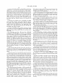
priority interrupt signals output from the slave controllers
simplicity, the discussion of the registers of FIGS. 5B and
5C will discuss only bit locations of primary importance to
the subject matter herein. Bit location [3] sets the level
triggered interrupt mode. If bit [3] is set to Zero, edge
sensitive interrupt detection is enabled and if set to 1, level
sensitive interrupt detection is enabled. Bit location [1],
SNGL sets the single PIC mode. Speci?cally, set to 0, the
system is con?gured in a cascade mode, while if set to 1,
only a single PIC system is enabled. Setting this bit to 1 then
170 and 172 could be used to route certain interrupt sources
from the slave controllers to any selected input to the master
controller. Software control would continue to maintain
PC/AT compatibility by ensuring the PC/AT priority
scheme. Another embodiment would require additional
hardware i.e. increased additional slave controllers which
would effectively increase priority interrupt channels to the
entire system up to a maximum of 64 priority interrupt
channels by using 8 slave controllers cascaded onto master
controller. This would allow systems to take advantage of a
signi?cant increase the number of interrupt sources possible.
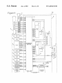
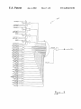
Also shown in FIG. 4 is a set of con?guration registers
166 coupled to the interrupt router 168. The con?guration
registers 166 control the PIC 48 of the microcontroller M.
10
the master PIC. In routing the interrupt request from slave 1
and slave 2 directly to IR2 and IRS of the master PIC
15
The con?guration registers 166 include both memory
mapped and direct-mapped registers. The memory-mapped
registers of the PIC 48 are mapped into the memory-mapped
con?guration register space of the microcontroller M.
mapping for both the internal peripheral sources listed above
and for eXternal sources connected to the buses 72 and 82.
25
compatible system.
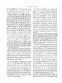
FIG. 5A is a block diagram of one of the memory-mapped
registers of the microcontroller M known as an interrupt
control register 167. The bottom three bits control the global
interrupt mode enable feature for each of the master 160, the
slave 162, and the slave 164. For example, if bit 0 of the
interrupt control register 167 is set, the global interrupt mode
for the master PIC 162 is enabled. The global interrupt mode
allows the individual controller to either recogniZe the edge
or level sensitive interrupts (at its 8 inputs) either globally or
individually. For PC/AT compatibility, bits 1 and 0 of the
interrupt control register 167 are set, while bit 2 is cleared.
respectively. Continuing, the master PIC operation control
ler 2 (MPICOCW2) is the register providing control for
various interrupt priority control and end of interrupt of
modes. Bits [2:0] set the speci?c end of interrupt level select.
Binary values 000—111b select for IRQO—IRQ7 respectively.
Master PIC operation controller 3 (MPICOCW3) provides
control for IRR/ISR register reads, master and poll modes.
Master PIC initialiZation control word 2 (MPICICW2) is the
second initialiZation register of the master controller. Bit
Among other functions, these registers control the interrupt
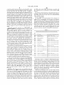
The direct-mapped registers are accessible in the PC/AT I/O
address space of the microcontroller M. Refer to Table 2,
below, for particular I/O port assignments for a PC/AT
will logically remove slave 1 and slave 2 controllers from
35
locations [7:3] identify the base interrupt vector number. For
eXample, these bits will be programmed to 00001b for the
master PIC (IRQO generates INT8), and 01110b for the slave
PIC (IRQ8 corresponds to INT 70h) in a PC/AT compatible
system. Further, bit locations [2:0] represent bit locations
A10 through A8 of the interrupt vector. These bits are always
0 in a PC/AT compatible system.
Turning to FIG. 5C, additional con?guration registers are
shown. The master PIC initialiZation control word 3
(MPICICW3) is the third initialiZation register of the master
controller. This register controls the slave cascading con
?guration for the various interrupt channels. For each bit
location, a 0 couples the respective device to the respective
IRQ input. When bit location is set to 1, then the respective
IRQ input is used for slave cascading. If bits 2 and 5 of this
register are cleared, both slave controllers are logically
removed from the cascade chain to the master controller and
Upon power-on-reset, these bits are ‘set’ to further maintain
only 8 interrupt request priority levels are available to the
PC/AT compatibility.
user. Continuing, the master PIC initialiZation controller 4
Con?guration/InitialiZation
(MPICICW4) is the fourth initialiZation register of the
master controller. InitialiZation of this register is optional
unless bit location [0] of register MPICICW1 is set.
The PIC 48 includes a set of con?guration registers 166,
as shown in FIG. 5. These registers include an interrupt
request register, in-service registers, interrupt mask register,
four initialiZation control words, and 2 operation control
45
words per controller.
Continuing, the master PIC interrupt mask (MPICINTMSK)
provides masking of individual interrupt request for the
master controller. A 0 value in any bit location unmasks the
respective IRQ signal. Alternatively a 1 in a bit location
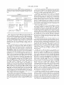
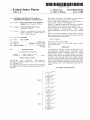
The register names are:
masks the respective interrupt input.
A set of such registers is available for each controller 160,
162, and 164. Additional registers could be added to the
Master Controller
Slave Controller 1
Slave Controller 2
system with only minor modi?cation for applications
MPICICW1
MPICICWZ
MPICICW3
MPICICW4
MPICOCWZ
MPICOCW3
MPICOCW1
S1PICICW1
S1PICICW2
S1PICICW3
S1PICICW4
S1PICOCW2
S1PICOCW3
S1PICOCW1
S2PICICW1
SZPICICWZ
S2PICICW3
S2PICICW4
SZPICOCWZ
S2PICOCW3
S2PICOCW1
involving more than two slave controllers, as discussed
(also known as IntI
mask register)
55
(also known as IntI mask (also known as IntI mask
register)
correspond to the I/O port assignments required for PC/AT
register)
compatibility.
The initialiZation of the PIC 48 consists of writing a
sequence of two to four bytes to each of the master PIC 160,
the slave PIC 162, and the slave PIC 164. The ?rst initial
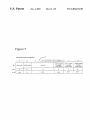
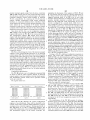
FIGS. 5B and 5C illustrate the various con?guration
registers of an embodiment. These will be described in the
conteXt of the master controller. Minor differences eXist for
analogous slave controller registers. Turning speci?cally to
FIG. 5B shown are 4 of the 7 con?guration registers. The
master PIC initialiZation control word 1 (MPICICW1) is the
?rst initialiZation register of the master controller. For
above. These are direct-mapped registers assigned to I/O
ports 20h—21h for the master PIC 160, 24h—25h for the slave
PIC 164, and 0A0h—0A1h for the slave PIC 162 of the
microcontroller M. The I/O port assignments for the master
PIC 160 and the slave PIC 162 for the microcontroller M
65
iZation byte is written to the lower address of each interrupt
controller (020h for the master 160, OAOh for the slave 164,
and 024h for the slave 162). All subsequent initialiZation
bytes are written to the upper address of the interrupt
controllers (021h for the master 160, 0A1h for the slave 164,