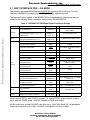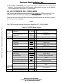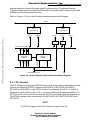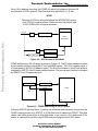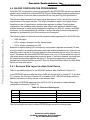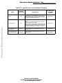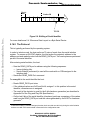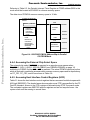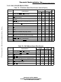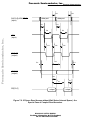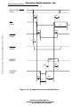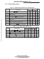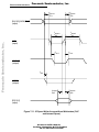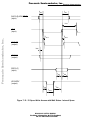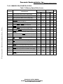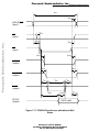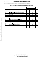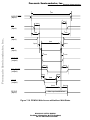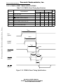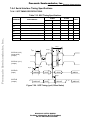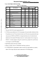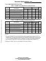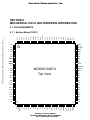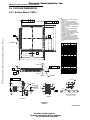
1
Freescale Semiconductor, Inc. Freescale Semiconductor, Inc... MC68SC302 Passive ISDN Protocol Engine User’s Manual 1997 Motorola, Inc. All Rights Reserved For More Information On This Product, Go to: www.freescale.com Freescale Semiconductor, Inc... Freescale Semiconductor, Inc. Home Page: www.freescale.com email: [email protected] USA/Europe or Locations Not Listed: Freescale Semiconductor Technical Information Center, CH370 1300 N. Alma School Road Chandler, Arizona 85224 (800) 521-6274 480-768-2130 [email protected] Europe, Middle East, and Africa: Freescale Halbleiter Deutschland GmbH Technical Information Center Schatzbogen 7 81829 Muenchen, Germany +44 1296 380 456 (English) +46 8 52200080 (English) +49 89 92103 559 (German) +33 1 69 35 48 48 (French) [email protected] Japan: Freescale Semiconductor Japan Ltd. Headquarters ARCO Tower 15F 1-8-1, Shimo-Meguro, Meguro-ku Tokyo 153-0064, Japan 0120 191014 +81 2666 8080 [email protected] Asia/Pacific: Freescale Semiconductor Hong Kong Ltd. Technical Information Center 2 Dai King Street Tai Po Industrial Estate, Tai Po, N.T., Hong Kong +800 2666 8080 [email protected] For Literature Requests Only: Freescale Semiconductor Literature Distribution Center P.O. Box 5405 Denver, Colorado 80217 (800) 441-2447 303-675-2140 Fax: 303-675-2150 LDCForFreescaleSemiconductor @hibbertgroup.com ii Information in this document is provided solely to enable system and software implementers to use Freescale Semiconductor products. There are no express or implied copyright licenses granted hereunder to design or fabricate any integrated circuits or integrated circuits based on the information in this document. Freescale Semiconductor reserves the right to make changes without further notice to any products herein. Freescale Semiconductor makes no warranty, representation or guarantee regarding the suitability of its products for any particular purpose, nor does Freescale Semiconductor assume any liability arising out of the application or use of any product or circuit, and specifically disclaims any and all liability, including without limitation consequential or incidental damages. “Typical” parameters which may be provided in Freescale Semiconductor data sheets and/or specifications can and do vary in different applications and actual performance may vary over time. All operating parameters, including “Typicals” must be validated for each customer application by customer’s technical experts. Freescale Semiconductor does not convey any license under its patent rights nor the rights of others. Freescale Semiconductor products are not designed, intended, or authorized for use as components in systems intended for surgical implant into the body, or other applications intended to support or sustain life, or for any other application in which the failure of the Freescale Semiconductor product could create a situation where personal injury or death may occur. Should Buyer purchase or use Freescale Semiconductor products for any such unintended or unauthorized application, Buyer shall indemnify and hold Freescale Semiconductor and its officers, employees, subsidiaries, affiliates, and distributors harmless against all claims, costs, damages, and expenses, and reasonable attorney fees arising out of, directly or indirectly, any claim of personal injury or death associated with such unintended or unauthorized use, even if such claim alleges that Freescale Semiconductor was negligent regarding the design or manufacture of the part. MC68SC302 USER’S MANUAL For More Information On This Product, Go to: www.freescale.com Information in this document is provided solely to enable system and software implementers to use Freescale Semiconductor products. There are no express or implied copyright licenses granted hereunder to design or fabricate any integrated circuits or integrated circuits based on the information in this document. Freescale Semiconductor reserves the right to make changes without further notice to any products herein. Freescale Semiconductor makes no warranty, representation or guarantee regarding the suitability of its products for any particular purpose, nor does Freescale Semiconductor assume any liability arising out of the application or use of any product or circuit, and specifically disclaims any and all liability, including without limitation consequential or incidental damages. “Typical” parameters which may be provided in Freescale Semiconductor data sheets and/or specifications can and do vary in different applications and actual performance may vary over time. All operating parameters, including “Typicals” must be validated for each customer application by customer’s technical experts. Freescale Semiconductor does not convey any license under its patent rights nor the rights of others. Freescale Semiconductor products are not designed, intended, or authorized for use as components in systems intended for surgical implant into the body, or other applications intended to support or sustain life, or for any other application in which the failure of the Freescale Semiconductor product could create a situation where personal injury or death may occur. Should Buyer purchase or use Freescale Semiconductor products for any such unintended or unauthorized application, Buyer shall indemnify and hold Freescale Semiconductor and its officers, employees, subsidiaries, affiliates, and distributors harmless against all claims, costs, damages, and expenses, and reasonable attorney fees arising out of, directly or indirectly, any claim of personal injury or death associated with such unintended or unauthorized use, even if such claim alleges that Freescale Semiconductor was negligent regarding the design or manufacture of the part. Freescale Semiconductor, Inc. PREFACE The complete documentation package for the MC68SC302 consists of the MC68SC302 Passive ISDN Protocol Engine User’s Manual, and the MC68SC302/D, MC68SC302 Passive ISDN Protocol Engine Product Brief. The MC68SC302 Passive ISDN Protocol Engine User’s Manual describes the programming, capabilities, registers, and operation of the MC68SC302; and the MC68SC302 Passive ISDN Protocol Engine Product Brief provides a brief description of the MC68SC302 capabilities. Freescale Semiconductor, Inc... This user’s manual is organized as follows: Section 1 Section 2 Section 3 Section 4 Section 5 Section 6 Section 7 Section 8 Introduction Signal Description Interrupts and Timer Communications Processor (CP) ISA Plug And Play Interface PCMCIA Interface Electrical Characteristics Mechanical Data And Ordering Information ELECTRONIC SUPPORT: Internet access is provided through the World Wide Web at http://www.mot.com/netcomm. — Sales Offices — For questions or comments pertaining to technical information, questions, and applications, please contact one of the following sales offices nearest you. MC68SC302 USER’S MANUAL For More Information On This Product, Go to: www.freescale.com Freescale Semiconductor, Inc. UNITED STATES Freescale Semiconductor, Inc... ALABAMA, Huntsville ARIZONA, Tempe CALIFORNIA, Agoura Hills CALIFORNIA, Los Angeles CALIFORNIA, Irvine CALIFORNIA, Rosevllle CALIFORNIA, San Diego CALIFORNIA, Sunnyvale COLORADO, Colorado Springs COLORADO, Denver CONNECTICUT, Wallingford FLORIDA, Maitland FLORIDA, Pompano Beach/ Fort Lauderdal FLORIDA, Clearwater GEORGlA, Atlanta IDAHO, Boise ILLINOIS, Chicago/Hoffman Estates INDlANA, Fort Wayne INDIANA, Indianapolis INDIANA, Kokomo IOWA, Cedar Rapids KANSAS, Kansas City/Mission MARYLAND, Columbia CANADA BRITISH COLUMBIA, Vancouver ONTARIO, Toronto ONTARIO, Ottawa QUEBEC, Montreal (305) 486-9776 (813) 538-7750 (404) 729-7100 (208) 323-9413 (708) 490-9500 (219) 436-5818 (317) 571-0400 (317) 457-6634 (319) 373-1328 (913) 451-8555 (410) 381-1570 (604) 293-7605 (416) 497-8181 (613) 226-3491 (514) 731-6881 INTERNATIONAL AUSTRALIA, Melbourne AUSTRALIA, Sydney BRAZIL, Sao Paulo CHINA, Beijing FINLAND, Helsinki Car Phone FRANCE, Paris/Vanves GERMANY, Langenhagen/ Hanover GERMANY, Munich GERMANY, Nuremberg GERMANY, Sindelfingen GERMANY,Wiesbaden HONG KONG, Kwai Fong Tai Po INDIA, Bangalore ISRAEL, Tel Aviv ITALY, Milan JAPAN, Aizu JAPAN, Atsugi JAPAN, Kumagaya JAPAN, Kyushu JAPAN, Mito JAPAN, Nagoya JAPAN, Osaka JAPAN, Sendai JAPAN, Tachikawa JAPAN, Tokyo JAPAN, Yokohama KOREA, Pusan KOREA, Seoul iv (205) 464-6800 (602) 897-5056 (818) 706-1929 (310) 417-8848 (714) 753-7360 (916) 922-7152 (619) 541-2163 (408) 749-0510 (719) 599-7497 (303) 337-3434 (203) 949-4100 (407) 628-2636 (61-3)887-0711 (61(2)906-3855 55(11)815-4200 86 505-2180 358-0-35161191 358(49)211501 33(1)40 955 900 49(511)789911 49 89 92103-0 49 911 64-3044 49 7031 69 910 49 611 761921 852-4808333 852-6668333 (91-812)627094 972(3)753-8222 39(2)82201 81(241)272231 81(0462)23-0761 81(0485)26-2600 81(092)771-4212 81(0292)26-2340 81(052)232-1621 81(06)305-1801 81(22)268-4333 81(0425)23-6700 81(03)3440-3311 81(045)472-2751 82(51)4635-035 82(2)554-5188 MASSACHUSETTS, Marborough MASSACHUSETTS, Woburn MICHIGAN, Detroit MINNESOTA, Minnetonka MISSOURI, St. Louis NEW JERSEY, Fairfield NEW YORK, Fairport NEW YORK, Hauppauge NEW YORK, Poughkeepsie/Fishkill NORTH CAROLINA, Raleigh OHIO, Cleveland OHIO, Columbus Worthington OHIO, Dayton OKLAHOMA, Tulsa OREGON, Portland PENNSYLVANIA, Colmar Philadelphia/Horsham TENNESSEE, Knoxville TEXAS, Austin TEXAS, Houston TEXAS, Plano VIRGINIA, Richmond WASHINGTON, Bellevue Seattle Access WISCONSIN, Milwaukee/Brookfield MALAYSIA, Penang MEXICO, Mexico City MEXICO, Guadalajara Marketing Customer Service NETHERLANDS, Best PUERTO RICO, San Juan SINGAPORE SPAIN, Madrid or SWEDEN, Solna SWITZERLAND, Geneva SWITZERLAND, Zurich TAlWAN, Taipei THAILAND, Bangkok UNITED KINGDOM, Aylesbury (508) 481-8100 (617) 932-9700 (313) 347-6800 (612) 932-1500 (314) 275-7380 (201) 808-2400 (716) 425-4000 (516) 361-7000 (914) 473-8102 (919) 870-4355 (216) 349-3100 (614) 431-8492 (513) 495-6800 (800) 544-9496 (503) 641-3681 (215) 997-1020 (215) 957-4100 (615) 690-5593 (512) 873-2000 (800) 343-2692 (214) 516-5100 (804) 285-2100 (206) 454-4160 (206) 622-9960 (414) 792-0122 60(4)374514 52(5)282-2864 52(36)21-8977 52(36)21-9023 52(36)669-9160 (31)49988 612 11 (809)793-2170 (65)2945438 34(1)457-8204 34(1)457-8254 46(8)734-8800 41(22)7991111 41(1)730 4074 886(2)717-7089 (66-2)254-4910 44(296)395-252 FULL LINE REPRESENTATIVES COLORADO, Grand Junction Cheryl Lee Whltely (303) 243-9658 KANSAS, Wichita Melinda Shores/Kelly Greiving (316) 838 0190 NEVADA, Reno Galena Technology Group (702) 746 0642 NEW MEXICO, Albuquerque S&S Technologies, lnc. (505) 298-7177 UTAH, Salt Lake City Utah Component Sales, Inc. (801) 561-5099 WASHINGTON, Spokane Doug Kenley (509) 924-2322 ARGENTINA, Buenos Aires Argonics, S.A. (541) 343-1787 HYBRID COMPONENTS RESELLERS Elmo Semiconductor (818) 768-7400 Minco Technology Labs Inc. (512) 834-2022 Semi Dice Inc. (310) 594-4631 MC68SC302 USER’S MANUAL For More Information On This Product, Go to: www.freescale.com Freescale Semiconductor, Inc. TABLE OF CONTENTS Paragraph Number Title Page Number Freescale Semiconductor, Inc... PREFACE ELECTRONIC SUPPORT:......................................................................... iii — Sales Offices —..................................................................................... iii 1.1 1.2 1.3 1.4 1.5 Section 1 MC68SC302 Overview MC68SC302 Key Features ..................................................................... 1-1 MC68SC302 Overview............................................................................ 1-4 Reference Designs.................................................................................. 1-5 MC68SC302 Application Development System...................................... 1-7 ADS Features.......................................................................................... 1-7 2.1 2.1.1 2.1.1.1 2.1.1.2 2.1.2 2.1.2.1 2.1.2.2 2.1.3 2.1.3.1 2.1.3.2 2.1.3.3 2.1.3.4 2.1.3.5 2.1.3.6 2.1.3.7 2.1.3.8 2.1.3.9 2.1.3.10 2.1.3.11 2.1.3.12 2.1.4 2.1.4.1 2.1.4.2 2.1.5 Section 2 Signal Description and Pin Control Host Interface Pins – ISA Mode .............................................................. 2-3 Address Bus Pins.................................................................................... 2-4 Latched Address Bus Pins (LA23—LA17) .............................................. 2-4 Static Address Bus Pins (SA16—SA0) ................................................... 2-4 Data Bus Pins (SD15—SD0) .................................................................. 2-4 Low Data Bus Pins (SD7–SD0) .............................................................. 2-4 High Data Bus Pins (SD15—SD8) .......................................................... 2-4 Bus Control Pins ..................................................................................... 2-4 AEN—Address Enable pin ...................................................................... 2-4 BALE—Bus Address Latch Enable ......................................................... 2-4 SBHE—System Bus High Enable ........................................................... 2-4 MEMR—Memory Read ........................................................................... 2-5 MEMW—Memory Write .......................................................................... 2-5 IOR—I/O Read........................................................................................ 2-5 IOW/PC_Mode—I/O Write and PC_Mode .............................................. 2-5 MEMCS16—Memory Cycle Select is 16 Bit ........................................... 2-5 IOCS16—I/O Cycle Select is 16 Bi ......................................................... 2-5 IOCHRDY—I/O Channel Ready ............................................................. 2-5 REF—Refresh......................................................................................... 2-5 RESET — Reset ..................................................................................... 2-5 Interrupt Out Pins .................................................................................... 2-6 IRQ9, 10, 11, 12, 15 — Dedicated mode ................................................ 2-6 IRQO, IRQSEL3–IRQSEL0 — Encoded Mode....................................... 2-6 Clock Pins ............................................................................................... 2-6 MC68SC302 USER’S MANUAL For More Information On This Product, Go to: www.freescale.com Table of Contents Freescale Semiconductor, Inc... Paragraph Number 2.1.5.1 2.1.5.2 2.1.5.3 2.2 2.2.1 2.2.1.1 2.2.1.2 2.2.2 2.2.2.1 2.2.3 2.2.3.1 2.2.3.2 2.2.3.3 2.2.3.4 2.2.3.5 2.2.3.6 2.2.3.7 2.2.3.8 2.2.3.9 2.2.3.10 2.2.3.11 2.2.3.12 2.2.4 2.2.4.1 2.2.4.2 2.2.4.3 2.3 2.3.1 2.3.1.1 2.3.1.2 2.3.1.3 2.3.1.4 2.3.1.5 2.3.1.6 2.3.2 2.3.2.1 2.3.2.2 2.3.2.3 2.3.2.4 2.3.2.5 2.3.2.6 2.3.2.7 2.3.2.8 Freescale Semiconductor, Inc. Title Page Number EXTAL—External Clock/Crystal Input......................................................2-6 XTAL— Crystal Output ............................................................................2-6 CLKO— Clock Out...................................................................................2-7 Host Interface Pins - PCMCIA Mode .......................................................2-7 Address Bus Pins.....................................................................................2-8 PC_A[21:17]/IRQIN[5:1]/PA[15:12]—PCMCIA Address Bus...................2-8 Address Bus Pins. PC_A[16:0]–PCMCIA Address Bus...........................2-8 Data Bus Pins ..........................................................................................2-8 PC_D[15:0]—PCMCIA Data Bus .............................................................2-8 Bus Control Pins ......................................................................................2-8 PC_MODE—PCMCIA Mode....................................................................2-8 PC_E2E—PCMCIA Serial EEPROM mode.............................................2-8 PC_CE1 and PC_CE2— PCMCIA Card Enables 1 and 2.......................2-8 PC_OE—PCMCIA Output Enable ...........................................................2-8 PC_WE—PCMCIA Write Enable .............................................................2-8 PC_A25—PCMCIA Address Bus bit 25...................................................2-8 PC_CISCS—PCMCIA CIS Chip Select ...................................................2-8 PC_STSCHG—PCMCIA Status Changed (Replace BVD1)....................2-8 PC_WAIT—PCMCIA Wait .......................................................................2-9 PC_REG—PCMCIA Attribute Memory Select .........................................2-9 RESET— Hard System Reset Input ........................................................2-9 IRQ3/PC_READY/IREQ— Ready or Interrupt Request Out Pin .............2-9 Clock Pins ................................................................................................2-9 EXTAL—External Clock/Crystal Input......................................................2-9 XTAL— Crystal Output ............................................................................2-9 CLKO— Clock Out...................................................................................2-9 Peripheral Pins.......................................................................................2-10 ISDN Pins ..............................................................................................2-10 L1RXD—Layer-1 Receive Data .............................................................2-10 L1TXD—Layer-1 Transmit Data ............................................................2-11 L1CLK—Layer-1 Clock ..........................................................................2-11 L1SYNC—Layer-1 Sync ........................................................................2-11 L1GRNT / PSYNC —Layer-1 Grant / PCM SYNC.................................2-11 L1RQ / GCIDCL—Layer-1 Request / GCI Clock Out.............................2-11 NMSI Pins ..............................................................................................2-11 RXD—SCC Receive Data Pin ...............................................................2-11 TXD—SCC Transmit Data Pin...............................................................2-11 TCLK / MCLK —SCC Transmit Clock Pin / Codec Main Clock .............2-11 RCLK / SCLK / IRQIN1 —SCC2 Receive Clock / Codec Serial Clock / Interrupt Request In 1 Pin ......................................................................2-11 SDS1 / FSYN / IRQIN2—Serial Data Strobe 1 / Codec Frame Sync / Interrupt Request In 2 Pin .....................................................................2-11 SDS2 / IRQIN3—Serial Data Strobe 2 / Interrupt Request In 3 Pin.......2-12 NMSICS—NMSI Chip Select Pin...........................................................2-12 RI / IRQIN4—Ring Indicate / Interrupt Request In 4 Pin........................2-12 MC68SC302 USER’S MANUAL For More Information On This Product, Go to: www.freescale.com Freescale Semiconductor, Inc. Freescale Semiconductor, Inc... Paragraph Number Title Table of Contents Page Number 2.3.3 2.3.3.1 2.3.3.2 2.3.3.3 2.3.3.4 2.3.3.5 2.3.4 2.3.4.1 2.3.4.2 2.3.4.3 2.3.4.4 2.3.4.5 2.3.4.6 SCP Pins ............................................................................................... 2-12 SPRXD—SCP Receive Serial Data Pin ................................................ 2-12 SPTXD—SCP Transmit Serial Data Pin ............................................... 2-12 SPCLK—SCP Clock Pin ....................................................................... 2-12 E2EN—EEPROM Enable Pin ............................................................... 2-12 SCPEN1-3 —SCP Slave Enable 1-3 Pins ............................................ 2-12 Multi-Function I/O Pins .......................................................................... 2-12 PORT A ................................................................................................. 2-13 Port A Registers .................................................................................... 2-14 Port A SCP Enable Control ................................................................... 2-15 Multi-Function Pins................................................................................ 2-15 Pin Multi-Function Select Register (PMFSR) ........................................ 2-16 Special Pin Function in 8-Bit Mode ....................................................... 2-16 3.1 3.1.1 3.1.2 3.1.3 3.1.4 3.1.5 3.1.6 3.1.7 3.1.8 3.1.8.1 3.1.8.2 3.1.8.3 3.2 Section 3 Interrupt, Timer, and Power Control Interrupt Controller .................................................................................. 3-1 Interrupt Controller Overview .................................................................. 3-1 Masking Interrupt Sources and Events ................................................... 3-1 Interrupt Handling Procedure .................................................................. 3-2 Wake Up On Interrupt ............................................................................. 3-2 Global Interrupt Mode Register (GIMR) .................................................. 3-3 Interrupt Pending Register (IPR) ............................................................. 3-3 Interrupt Mask Register (IMR) ................................................................. 3-4 Periodic Interrupt Timer........................................................................... 3-4 Overview ................................................................................................. 3-4 Periodic Timer Period Calculation ........................................................... 3-4 Periodic Interrupt Timer Register (PITR)................................................. 3-5 ISA Power Control Registers................................................................... 3-5 4.1 4.2 4.2.1 4.3 4.3.1 4.3.2 4.3.3 4.3.4 4.4 4.4.1 4.4.2 4.5 4.5.1 4.5.2 Section 4 Communications Processor (CP) Main Controller ........................................................................................ 4-1 Command Set ......................................................................................... 4-2 Command Execution Latency ................................................................. 4-4 Serial Channels Physical Interface.......................................................... 4-4 IDL Interface............................................................................................ 4-5 GCI Interface ........................................................................................... 4-7 PCM Highway Mode................................................................................ 4-9 Nonmultiplexed Serial Interface (NMSI) ................................................ 4-12 Serial Interface Registers ...................................................................... 4-12 Serial Interface Mode Register (SIMODE) ............................................ 4-12 Serial Interface Mask Register (SIMASK) ............................................. 4-14 Serial Communication Controllers (SCC).............................................. 4-15 SCC Features........................................................................................ 4-16 SCC Mode Register (SCM) ................................................................... 4-16 MC68SC302 USER’S MANUAL For More Information On This Product, Go to: www.freescale.com Table of Contents Freescale Semiconductor, Inc... Paragraph Number 4.5.3 4.5.4 4.5.5 4.5.5.1 4.5.5.2 4.5.5.3 4.5.5.4 4.5.5.5 4.5.5.6 4.5.5.7 4.5.5.8 4.5.5.9 4.5.6 4.5.7 4.5.8 4.5.9 4.5.10 4.5.10.1 4.5.10.2 4.5.10.3 4.5.10.4 4.5.10.5 4.5.10.6 4.5.10.7 4.5.10.8 4.5.10.9 4.5.10.10 4.5.10.11 4.5.11 4.5.11.1 4.5.11.2 4.5.11.3 4.5.11.4 4.5.11.5 4.5.11.6 4.5.11.7 4.5.11.8 4.5.11.9 4.5.11.10 4.5.12 4.5.12.1 4.5.12.2 4.5.12.3 4.6 4.6.1 Freescale Semiconductor, Inc. Title Page Number SCC Transmit Buffer Descriptors...........................................................4-18 SCC Receive Buffer Descriptors............................................................4-19 SCC Parameter RAM.............................................................................4-23 RX BD Table Pointer (RBASE) ..............................................................4-23 RX Chunk Length (RLEN)......................................................................4-23 RX Interrupt Threshold (RTHRSH) ........................................................4-23 CPU First Not Handled BD (RNH) .........................................................4-23 RX Time-OUT(RTO) ..............................................................................4-23 Maximum Receive Buffer Length Register (MRBLR) ............................4-24 RX Current BD (RCBD) .........................................................................4-24 TX BD Table Pointer (TBASE)...............................................................4-24 Transmitter Buffer Descriptor Pointer (TBPTR) .....................................4-24 SCC Event Register (SCCE) .................................................................4-25 SCC Mask Register (SCCM) .................................................................4-25 SCC Status Register (SCCS) ................................................................4-26 Disabling the SCCs................................................................................4-26 HDLC Controller.....................................................................................4-27 HDLC Channel Frame Transmission Processing ..................................4-28 HDLC Channel Frame Reception Processing .......................................4-29 HDLC Memory Map ...............................................................................4-29 HDLC Programming Model....................................................................4-30 HDLC Command Set .............................................................................4-30 HDLC Address Recognition ...................................................................4-31 HDLC Error-Handling Procedure ...........................................................4-31 HDLC Receive Buffer Descriptor (Rx BD) .............................................4-32 HDLC Transmit Buffer Descriptor (TxBD)..............................................4-33 HDLC Event Register.............................................................................4-35 HDLC Mask Register .............................................................................4-36 Transparent Controller ...........................................................................4-36 Transparent Channel Buffer Transmission Processing .........................4-36 Transparent Channel Buffer Reception Processing...............................4-37 Transparent Memory Map......................................................................4-38 Transparent Commands ........................................................................4-38 Transparent Synchronization .................................................................4-39 Transparent Error-Handling Procedure..................................................4-39 Transparent Receive Buffer Descriptor (RxBD).....................................4-40 Transparent Transmit Buffer Descriptor (TxBD) ....................................4-41 Transparent Event Register ...................................................................4-42 Transparent Mask Register....................................................................4-43 SCC2/3 Clocking in NMSI mode............................................................4-43 SCC2/3 NMSI Interface .........................................................................4-43 SCC2/3 CODEC Interface .....................................................................4-43 Configuration Register (SCON) .............................................................4-44 Serial Communication Port (SCP) .........................................................4-47 SCP Programming Model ......................................................................4-47 MC68SC302 USER’S MANUAL For More Information On This Product, Go to: www.freescale.com Freescale Semiconductor, Inc. Freescale Semiconductor, Inc... Paragraph Number Title Table of Contents Page Number 4.6.2 4.6.3 4.6.3.1 4.6.3.2 4.6.3.2.1 4.6.3.2.2 4.6.3.2.3 4.7 4.7.1 4.7.1.1 4.7.2 4.7.3 4.7.4 4.7.4.1 4.7.4.2 4.7.4.3 4.7.4.4 4.7.5 4.8 SCP Clock and Data Relationship......................................................... 4-49 SCP Transmit/Receive Buffer Descriptor .............................................. 4-49 SCP Data Transmit/Receive Processing............................................... 4-50 SCP - Serial EEPROM interface ........................................................... 4-50 16- Bit Address EEPROM ..................................................................... 4-50 8-Bit Address EEPROM ........................................................................ 4-51 Mixed Address EEPROM ...................................................................... 4-52 Serial Management Controllers (SMCs)................................................ 4-52 SMC Overview ...................................................................................... 4-52 Using GCI with the SMCs...................................................................... 4-52 SMC Programming Model ..................................................................... 4-54 SMC Commands ................................................................................... 4-54 SMC Memory Structure and Buffers Descriptors .................................. 4-54 SMC1 Receive Buffer Descriptor .......................................................... 4-55 SMC1 Transmit Buffer Descriptor ......................................................... 4-56 SMC2 Receive Buffer Descriptor .......................................................... 4-56 SMC2 Transmit Buffer Descriptor ......................................................... 4-57 SMC Interrupt Requests........................................................................ 4-57 Revision Number................................................................................... 4-58 5.1 5.2 5.3 5.3.1 5.3.1.1 5.3.1.2 5.3.2 5.3.3 5.3.3.1 5.3.3.2 5.3.3.3 5.4 5.4.1 5.4.2 5.4.3 5.4.4 5.4.5 5.4.6 5.4.7 5.4.8 5.5 5.6 5.7 5.7.1 Section 5 ISA Plug and Play Interface Introduction.............................................................................................. 5-1 Main Features ......................................................................................... 5-1 ISA Memory Map..................................................................................... 5-1 ISA I/O Address Space ........................................................................... 5-2 DPR Addressing...................................................................................... 5-4 CCR Addressing...................................................................................... 5-4 ISA Memory Address Space ................................................................... 5-4 CCMR Structure ...................................................................................... 5-4 DPR......................................................................................................... 5-5 Parameter RAM....................................................................................... 5-5 CCR Register Map .................................................................................. 5-5 ISA-PNP Configuration Programming ..................................................... 5-7 Resource Data Layout in a Byte Serial Device ....................................... 5-7 Reading Resource Data .......................................................................... 5-9 I/O Configuration ................................................................................... 5-10 Memory Configuration ........................................................................... 5-11 IRQ Configuration.................................................................................. 5-12 Resource Management ......................................................................... 5-12 Logical Device ID .................................................................................. 5-13 Unsupported Resources........................................................................ 5-13 ISA-PNP Card Level Control Registers................................................. 5-13 Logical Device Control Registers .......................................................... 5-19 ISA-PNP Configuration Registers ......................................................... 5-20 Access to Inactive Registers ................................................................. 5-25 MC68SC302 USER’S MANUAL For More Information On This Product, Go to: www.freescale.com Table of Contents Paragraph Number Freescale Semiconductor, Inc... 5.8 5.9 5.10 5.11 5.12 5.13 5.14 5.14.1 5.14.2 5.14.3 5.15 Freescale Semiconductor, Inc. Title Page Number ISA-PNP Control Registers Summary ...................................................5-26 ISA-PNP Configuration Registers Summary..........................................5-28 Card Configuration and Control Register Map (CCR)............................5-30 Host Interface Control Register Map (HCR) ..........................................5-33 ISA-PNP Physical Interface BAckground...............................................5-37 Initiation Key ..........................................................................................5-38 Isolation Protocol ...................................................................................5-38 General ..................................................................................................5-38 The Protocol...........................................................................................5-39 Timing Issues Related to Serial Isolation...............................................5-40 Run-Time Access to ISA-PNP ...............................................................5-41 6.4.2 6.4.3 6.4.4 6.4.5 6.5 6.5.1 6.5.1.1 6.5.1.2 6.5.2 6.6 6.6.1 6.6.2 6.7 6.7.1 6.7.1.1 6.7.1.2 6.7.1.3 6.7.2 6.7.3 6.7.4 Section 6 PCMCIA Interface Introduction ..............................................................................................6-1 PCMCIA Controller Key Features ............................................................6-1 PCMCIA Interface Functional Overview ..................................................6-1 PCMCIA Memory Map .............................................................................6-3 Accessing the HCR Region (Both Serial and Parallel Cis EEPROM Mode ........................................................................................................6-3 Accessing the CCMR Region in Serial CIS EEPROM Mode...................6-3 Accessing the CCMR in Parallel CIS EEPROM mode ............................6-4 Accessing the External Chip Select Space..............................................6-5 Accessing Host Interface Control Registers (HCR) .................................6-5 CCMR Memory Space .............................................................................6-6 Dual Ported RAM (DPR) ..........................................................................6-6 System RAM ............................................................................................6-7 Parameter RAM .......................................................................................6-7 CCR Register Map...................................................................................6-7 Host Interface Control registers (HCR) ....................................................6-8 PCMCIA Function Configuration Registers (FCR)...................................6-9 68SC302 Specific HCR Registers .........................................................6-11 PCMCIA bus Accesses..........................................................................6-16 SC302 Power Management...................................................................6-17 Enter Low Power....................................................................................6-17 Wake Up ................................................................................................6-17 READY...................................................................................................6-17 PCMCIA Host Interrupts ........................................................................6-18 Unimplemented PCMCIA Signals ..........................................................6-18 PCMCIA EEPROM Format ....................................................................6-18 7.1 7.2 7.3 Section 7 Electrical Characteristics Maximum Ratings ....................................................................................7-1 Thermal Characteristics ...........................................................................7-1 Power Considerations..............................................................................7-2 6.1 6.2 6.3 6.4 6.4.1 MC68SC302 USER’S MANUAL For More Information On This Product, Go to: www.freescale.com Freescale Semiconductor, Inc. Freescale Semiconductor, Inc... Paragraph Number Title Table of Contents Page Number 7.4 7.5 7.6 7.6.1 7.6.2 7.6.2.1 7.6.2.2 7.6.2.3 7.6.2.4 7.6.2.5 7.6.3 7.6.3.1 7.6.3.2 7.6.3.3 7.6.4 7.6.4.1 7.6.4.2 7.6.4.3 7.6.4.4 7.6.4.5 7.6.4.6 Power Dissipation.................................................................................... 7-2 DC Electrical Characteristics................................................................... 7-2 AC Electrical Specifications..................................................................... 7-4 CLKOUT Timing Specifications............................................................... 7-4 ISA Host Interface Timing Specifications ................................................ 7-6 ISA Reset Timing Specifications ............................................................. 7-6 ISA IO Space Read Access .................................................................... 7-7 IO Space Write Access ......................................................................... 7-13 Memory Space Read Access ................................................................ 7-16 Memory Space Write Access ................................................................ 7-19 PCMCIA Host Interface Timing Specifications ...................................... 7-22 PCMCIA Read Access with/without Wait States ................................... 7-22 PCMCIA Write Access with/without Wait States ................................... 7-24 PCMCIA Reset Timing Specifications .................................................. 7-26 Serial Interface Timing Specifications ................................................... 7-27 SCP Timing Specifications .................................................................... 7-27 SERIAL EEPROM Timing Specifications .............................................. 7-28 IDL Timing Specifications...................................................................... 7-31 GCI Timing Specifications ..................................................................... 7-33 PCM Timing Specifications ................................................................... 7-35 NMSI Timing Specifications .................................................................. 7-37 8.1 8.1.1 8.2 8.2.1 8.3 Section 8 Mechanical Data and Ordering Information Pin Assignments...................................................................................... 8-1 Surface Mount (TQFP ) ........................................................................... 8-1 Package Dimensions............................................................................... 8-2 Surface Mount (TQFP) ............................................................................ 8-2 Ordering Information ............................................................................... 8-3 MC68SC302 USER’S MANUAL For More Information On This Product, Go to: www.freescale.com Freescale Semiconductor, Inc. LIST OF FIGURES Freescale Semiconductor, Inc... Figure Number Figure 1-1. Figure 1-2. Figure 1-3. Figure 1-4. Figure 1-5. Figure 1-6. Title Page Number Section 1 MC68SC302 Overview MC68SC302 Block Diagram ......................................................................... 1-4 Passive NT1 TA Block Diagram.................................................................... 1-5 Passive NT1 TA Block Diagram with S/T Interface....................................... 1-6 NT1 TA Block Diagram with POTS Interface and Datapump ....................... 1-6 PC Card TA................................................................................................... 1-7 ADS Block Diagram ...................................................................................... 1-8 Section 2 Signal Description and Pin Control Figure 2-1. Functional Signal Groups Description (82 Pin) ............................................. 2-2 Figure 2-2. Parallel I/O Port A Registers ....................................................................... 2-14 Section 3 Interrupt, Timer, and Power Control Section 4 Communications Processor (CP) Figure 4-1. Serial Channels Physical Interface Block Diagram....................................... 4-5 Figure 4-2. Two PCM Sync Methods ............................................................................ 4-11 Figure 4-3. PCM Channel Assignment on a T1/CEPT Line .......................................... 4-11 Figure 4-4. SCC Block Diagram .................................................................................... 4-16 Figure 4-5. Transmit BD ................................................................................................ 4-19 Figure 4-7. Receive BD ................................................................................................. 4-19 Figure 4-6. SCC Transmit Memory Structure................................................................ 4-20 Figure 4-8. Rx Channel Memory Chunk........................................................................ 4-22 Figure 4-9. Typical HDLC Frame .................................................................................. 4-27 Figure 4-10. HDLC Address Recognition Examples ....................................................... 4-31 Figure 4-11. HDLC Receive Buffer Descriptor ................................................................ 4-32 Figure 4-12. HDLC Transmit Buffer Descriptor ............................................................... 4-34 Figure 4-13. Transparent Receive Buffer Descriptor....................................................... 4-40 Figure 4-14. Transparent Transmit Buffer Descriptor...................................................... 4-41 Figure 4-15. Codec Interface........................................................................................... 4-44 Figure 4-16. FSYN Timing............................................................................................... 4-44 Figure 4-17. SCC Baud Rate Generator ......................................................................... 4-46 Figure 4-18. SCP Clock and Data Relationship .............................................................. 4-49 MC68SC302 USER’S MANUAL For More Information On This Product, Go to: www.freescale.com Table of Contents Figure Number Freescale Semiconductor, Inc. Title Page Number Freescale Semiconductor, Inc... Figure 4-19. 16-Bit EEPROM Addressing....................................................................... 4-51 Figure 4-20. 8-Bit EEPROM Addressing......................................................................... 4-51 Figure 4-21. Mixed Address EEPROM Addressing ........................................................ 4-52 Section 5 ISA Plug and Play Interface Figure 5-1. SC302 Memory Spaces and Decoding Methods......................................... 5-2 Figure 5-2. HCR Access in ISA Mode............................................................................ 5-3 Figure 5-3. CCMR Addressing in ISA I/O Space ........................................................... 5-3 Figure 5-4. DPR Addressing .......................................................................................... 5-5 Figure 5-5. ISA-PNP Resource Data Layout in a Byte Serial EEPROM Device............. 5-9 Figure 5-6. Internal I/O Space Structure ...................................................................... 5-11 Figure 5-7. PNP - ISA Interconnection.......................................................................... 5-38 Figure 5-8. The LFSR Key Sequence ........................................................................... 5-38 Figure 5-9. Shifting of Serial Identifier........................................................................... 5-39 Figure 5-10. Isolation State Transitions .......................................................................... 5-41 Figure 6-1. Figure 6-2. Figure 6-3. Figure 6-4. Figure 6-5. Figure 6-6. Section 6 PCMCIA Interface Parallel EPROM Configuration ..................................................................... 6-2 Serial EEPROM Configuration...................................................................... 6-2 68SC302 PCMCIA Address Map in Serial CIS EEPROM Mode .................. 6-4 68SC302 PCMCIA Address Map in Parallel CIS PROM Mode .................... 6-5 DPR Addressing ........................................................................................... 6-6 RI to STSCHG Path.................................................................................... 6-11 Section 7 Electrical Characteristics Figure 7-1. CLKOUT Timing Specifications .................................................................... 7-4 Figure 7-2. CLKOUT Timing for CDIV 1-0=00 in CLKCNT ............................................ 7-5 Figure 7-3. CLKOUT Timing for CDIV 1-0=10 in CLKCNT ............................................ 7-5 Figure 7-4. CLKOUT Timing for CDIV 1-0=01 in CLKCNT ............................................ 7-5 Figure 7-5. ISA Reset Timing Specifications.................................................................. 7-6 Figure 7-6. IO Space Read Access without Wait States for PnP and Internal Space..... 7-8 Figure 7-7. IO Space Read Access without Wait States (PnP and Internal Space) the Special Case of Coupled Accesses........................................................ 7-9 Figure 7-8. IO Space Read Access without Wait States (Internal Space) .................... 7-10 Figure 7-9. IO Space Read Access without Wait States (Internal Space) the Special Case of Coupled Read Accesses ............................................ 7-11 Figure 7-10. IO Space Read Access with Wait States................................................... 7-12 Figure 7-11. IO Space Write Access without Wait states (PnP and Internal Space) .... 7-14 Figure 7-12. IO Space Write Access with Wait States - Internal Space......................... 7-15 Figure 7-13. Memory Space Read Access without Wait States..................................... 7-17 Figure 7-14. Memory Space Read Access with Wait States........................................... 7-18 Figure 7-15. Memory Space Write Access without Wait States...................................... 7-20 Figure 7-16. Memory Space Write Access with Wait States........................................... 7-21 MC68SC302 USER’S MANUAL For More Information On This Product, Go to: www.freescale.com Freescale Semiconductor, Inc. Freescale Semiconductor, Inc... Figure Number Title Table of Contents Page Number Figure 7-17. PCMCIA Read Access with/without Wait States......................................... 7-23 Figure 7-18. PCMCIA Write Access with/without Wait States ......................................... 7-25 Figure 7-19. PCMCIA Reset Timing Specifications....................................................... 7-26 Figure 7-20. SCP Timing (cp=0, Reset Value) ............................................................... 7-27 Figure 7-21. SCP Timing (cp=1)..................................................................................... 7-28 Figure 7-22. Serial EEPROM (SCP Type) Timing Specifications (with Initial Reset Value of spmode) ........................................................................................ 7-29 Figure 7-23. Serial EEPROM (93C46 TYPE) Timing Specifications (With Initial Reset Value of spmode).............................................................................. 7-30 Figure 7-24. IDL Timing Specifications............................................................................ 7-32 Figure 7-25. GCI Timing Specifications........................................................................... 7-34 Figure 7-26. PCM Timing Diagram (SYNC Envelopes Data) .......................................... 7-36 Figure 7-27. PCM Timing Diagram (SYNC Prior to 8-bit Data) ....................................... 7-36 Figure 7-28. NMSI Timing Specifications ........................................................................ 7-38 MC68SC302 USER’S MANUAL For More Information On This Product, Go to: www.freescale.com Freescale Semiconductor, Inc. LIST OF TABLES Freescale Semiconductor, Inc... Table Number Title Page Number Table 2-1 Table 2-2 Table 2-3 Table 2-4 Table 2-5 Section 2 Signal Description and Pin Control 2-1 MC68SC302 ISA Mode Signal Functional Groups ...................................... 2-3 PCMCIA Mode Signals ................................................................................ 2-7 Peripheral Pins .......................................................................................... 2-10 Multi-Function I/O Pin Function ................................................................. 2-14 Port A Pin Function.................................................................................... 2-16 Table 3-1 Table 3-2 Table 3-3 Table 3-4 Table 3-5 Table 3-6 Section 4 Communications Processor (CP) 4-1 ISDN Pin Functions in PCM Highway Mode ............................................... 4-9 Sync Signal Functions in PCM Highway Mode ......................................... 4-10 SCC Parameter RAM ............................................................................... 4-23 HDLC-Specific Parameter RAM ................................................................ 4-30 Transparent-Specific Parameter RAM ...................................................... 4-38 Clock Source Configuration Set Up .......................................................... 4-45 Table 5-1 Table 5-2 Table 5-3 Table 5-4 Table 5-5 Table 5-6 Table 5-7 Table 5-8 Table 5-9 Table 5-10 Table 5-11 Table 5-12 Table 5-13 Table 5-14 Section 5 ISA Plug and Play Interface 5-1 SC302 Parameter RAM .............................................................................. 5-5 CCR Register Map ...................................................................................... 5-6 Resource Data Layout ................................................................................ 5-7 Card Level Control Registers Summary ................................................... 5-26 Logical Device Control Registers Summary ............................................. 5-27 Memory Space Configuration Summary ................................................... 5-28 I/O Configuration Summary ...................................................................... 5-29 Interrupt Configuration Summary .............................................................. 5-29 DMA Configuration Registers Summary ................................................... 5-29 32-Bit Memory Space Configuration Summary ........................................ 5-29 Reserved and Vendor Defined Configuration Registers ........................... 5-30 Reserved Registers .................................................................................. 5-30 ISA-PNP Card Ports ................................................................................. 5-37 Serial Isolation Delays ............................................................................... 5-40 Table 6-1 Table 6-2 Table 6-3 Section 6 PCMCIA Interface 6-1 Host Interface Control Registers.................................................................. 6-6 SC302 PARAMETER RAM ........................................................................ 6-7 CCR Register Map...................................................................................... 6-8 MC68SC302 USER’S MANUAL For More Information On This Product, Go to: www.freescale.com Table of Contents Freescale Semiconductor, Inc... Table Number Freescale Semiconductor, Inc. Title Page Number Table 6-4 Table 6-5 Table 6-6 Table 6-7 Table 6-8 Table 6-9 Table 6-10 Table 6-11 Table 6-12 Table 6-13 Attribute Memory Read Access ................................................................ 6-16 Attribute Memory Write Access ................................................................ 6-16 Attribute CIS and HCR/FCR Accesses ..................................................... 6-16 CIS Locations ........................................................................................... 6-16 Common Memory Read Accesses ........................................................... 6-16 Common Memory Write Accesses ........................................................... 6-17 Low Power Modes .................................................................................... 6-17 Unmplemented PCMCIA Signals ............................................................. 6-18 16-Bit Address Serial EEPROM Format (93xxx) ....................................... 6-18 8-Bit Address Serial EEPROM Format (25xxx or 95xxx) ......................... 6-19 Table 7-1 Table 7-2 Table 7-3 Table 7-4 Table 7-5 Table 7-6 Table 7-7 Table 7-8 Table 7-9 Table 7-10 Table 7-11 Table 7-12 Table 7-13 Table 7-14 Table 7-15 Table 7-16 Table 7-17 Table 7-18 Table 7-19 Section 7 Electrical Characteristics 7-1 DC Electrical Characteristics (VCC = 5.0V ±5% ) ....................................... 7-2 CLKOUT Timing Specifications ................................................................... 7-4 ISA Reset Timing Specifications ................................................................ 7-6 IO Address Space Read Access (Internal Space) ...................................... 7-7 PnP Address Space Read Access ............................................................. 7-7 IO Address Space Write Access (Internal Space) .................................... 7-13 PnP Address Space Write Access ........................................................... 7-13 Memory Space Read Access ................................................................... 7-16 Memory Space Write Access ................................................................... 7-19 PCMCIA Read Access with/without Wait States ...................................... 7-22 PCMCIA Write Access with/without Wait States ...................................... 7-24 PCMCIA Reset Timing Specifications ..................................................... 7-26 SCP Timing Specifications ....................................................................... 7-27 SERIAL EEPROM Timing Specifications ................................................. 7-28 IDL Timing Specifications ......................................................................... 7-31 GCI Timing Specifications ........................................................................ 7-33 PCM Timing .............................................................................................. 7-35 NMSI Timing Specifications (External Clock) ........................................... 7-37 NMSI Timing Specifications (Internal Clock) ............................................ 7-37 MC68SC302 USER’S MANUAL For More Information On This Product, Go to: www.freescale.com Freescale Semiconductor, Inc. Freescale Semiconductor, Inc... SECTION 1 MC68SC302 OVERVIEW The MC68SC302 ISDN Passive ISDN Protocol Engine (PIPE) is an ISA Plug and Play/PC Card ISDN communication controller optimized for ISDN passive cards. The MC68SC302 is a descendant of the popular MC68302 Integrated Multiprotocol Processor. The microcoded RISC communications processor from the 68302 was modified to form the core of the 68SC302. The 68000 core and many related system integration features were removed to further optimize the device for passive ISDN card applications. The serial communication channels (SCC) have been optimized for supporting a full ISDN basic rate interface. The three SCCs support two 64kbit per second B-channels and one 16kbit per second D-channel. The 68SC302 connects gluelessly to Motorola’s MC145572 U transceiver or MC145574 S/T transceiver and, as an added bonus, eliminates the need for a second oscillator for the transceiver chip. 1.1 MC68SC302 KEY FEATURES • ISA Bus Interface — ISA Plug and Play — Glueless Connections to ISA — 24ma Buffers for ISA Bus Pins — Full Support of Plug and Play Standard — All Chip Registers Accessed from ISA Bus. — Support for 8 or 16 bit I/O or Memory ISA Cycles — 11 Selectable Interrupt Output Pins to ISA Bus. — Additional Chip Select Allows Another Device to Be Accessed from the ISA Bus. — Plug and Play Register Settings Stored in External Low Cost E2PROM. • PCMCIA Interface — PC Card 95 Compatible — Two CIS Storage Options: • CIS stored in Serial E2PROM and Downloaded At Runtime to Internal Dual Port RAM MC68SC302 USER’S MANUAL For More Information On This Product, Go to: www.freescale.com MC68SC302 Overview Freescale Semiconductor, Inc. • CIS Optionally Stored in Parallel E2PROM on the PC Card Bus with Dedicated Chip Select, Saving Dual Port RAM Buffer Space and Always Available for PC Accesses. — Memory Mode Accesses Supported (I/O Not Supported) — Supports 8/16 bit Memory Cycles — Supports Ring Detect through Status Change Pin — Additional Chip Select Allows Another Device to Be Address Mapped on the PC Card Bus. • ISDN Communications Processor Freescale Semiconductor, Inc... — Requires No External (Local) RAM — Flexible Channel Handling — RISC Processor Decreases CPU Load with Flexible Buffer Descriptor Structure and HDLC Capability. (UART Mode Not Supported) — Totally Independent Programming for Rx/Tx for each of the B and D Channels — Supports Any Sub-Channeling for Each of the B Channels — Enables a Concatenation of 2 B Channels (or Any Selected Bits) to a SuperChannel — HDLC with Retry Capability for the D Channel — Allows Dynamic Connection/Disconnection for each of the B Channels — Total 1536KB Dual Port RAM Divided into Parameter and Data Buffer RAM — 256 Byte Parameter RAM (As in PM302) — 1280 Byte Data RAM with Efficient FIFO Organization and Flexible Buffer Size — Independent Programmable Channel FIFO Length, if Split Equallyy: • 4 x 256 Bytes FIFO for B1 and B2 Channel (Rx/Tx) • 2 x 64 Bytes FIFO for D Channel (Rx/Tx) — Glueless Interface to Motorola and Other Popular ISDN S/T and U Interface Chips — Supports Motorola Interchip Digital Link (IDL) — Supports General Circuit Interface (GCI), Also Known as IOM-2TM TM IOM-2 is a trademark of Siemens Corporation. MC68SC302 USER’S MANUAL For More Information On This Product, Go to: www.freescale.com Freescale Semiconductor, Inc. MC68SC302 Overview — Includes Serial Communication Port (SCP) for Synchronous Communication — Includes one SMC That Can Support Both the C/I and Monitor Channel of GCI — Two Strobes Support Time-Slot Assignment of Non-Intelligent Peripherals — Only One Crystal Required for TA Application. — Clock Output (CLKO) Generation from a Crystal. CLKO Can Be Connected to S/T XTAL Input. — Clock Input for U-Chip (MC145572) Can Be Used to Drive SC302 Freescale Semiconductor, Inc... • Other System Integration Features — Gluelessly Connects to Serial E2PROM via SCP Port for Plug and Play ISA ID and CIS Storage. — 25XXX Series or 93XX Series E2PROMs Supported. — Flexible Pin Configuration Allows Trade-Offs Between 16-Bit Wide ISA/PC Card Interface and Extra I/O Pins. • Up to 16 Parallel I/O Pins for Controlling Other Functions. — On-Chip Interrupt Controller • 8 Internal Interrupt Sources • 7 External Pin Sources for External Devices. — 2 Low-Power Modes • Wait - Oscillator Keeps Running ~5 mA • Stop - Oscillator Stops - <100uA — Operating Speed: 0-20.48 Mhz — Operating Voltage: 5V — 100 pin TQFP (14mm x 14mm) The block diagram for the MC68SC302 is shown in Figure 1-1. The MC68SC302 architecture is based on a microcoded RISC communications processor that services the three main high speed serial channels (SCC), two serial management channels (SMC) and a serial communications port (SCP). The three SCC channels support simultaneous operation of the three channels specified by the ISDN basic rate interface (2B+D). Each SCC can support onboard HDLC processing as well as totally transparent operation. The dual-port RAM provides 1536 bytes of memory. A maximum of 1280 bytes can be allocated for serial channel buffer space, which, when allocated evenly for a basic rate interface, allows 256 bytes per B channel per direction and 64 bytes per direction for the D channel. This provides 32msec worth of basic rate data to be stored in the buffers, allowing ample interrupt latency time for host platform operating systems. The IDL or GCI interface provides direct connection to the Motorola MC145572 U interface transceiver, the MC145574 S/T MC68SC302 USER’S MANUAL For More Information On This Product, Go to: www.freescale.com MC68SC302 Overview Freescale Semiconductor, Inc. interface transceiver, and other popular ISDN transceivers. A non-multiplexed serial interface (NMSI) is also provided for SCC2. 1.2 MC68SC302 OVERVIEW PIO AND INTERRUPT PINS PIO AND INT I/F Freescale Semiconductor, Inc... SCC1 ISA PnP 1536 BYTE RAM COMMUNICATIONS PROCESSOR PCMCIA ISA PnP/ PCMCIA INTERFACE INTERFACE SCC2 SCC3 2 SMCs SCP IDL/GCI INTERFACE NMSI I/F SCP/E2 PROM INTERFACE NMSI PINS IDL/GCI PINS Figure 1-1. MC68SC302 Block Diagram The MC68SC302 has an ISA Plug and Play interface which supports the ISA Plug and Play specification version 1.0a. The ISA bus interface can be configured for either I/O mode accesses or memory mode accesses. The ISA interface can be either an 8- or 16- bit wide data bus allowing pin usage trade-offs to be made. I/O mode accesses are based on a selfincrementing pointer, allowing the PC to write or read data from a fixed ISA I/O address. Memory mode access allows the PC to write or read data into a predefined ISA window. In addition to supporting access to the internal MC68SC302 register and memory map, an additional chip-select is provided for an external device, and can be programmed for memory/IO and 8/16 bit bus independent of internal space. The MC68SC302 can also be configured to provide a PC Card interface based on the PC Card 95 specification. Either 8- or 16-bit wide memory cards can be implemented. There are two options available for supporting the Card Information Structure (CIS): 1)The CIS can MC68SC302 USER’S MANUAL For More Information On This Product, Go to: www.freescale.com Freescale Semiconductor, Inc. MC68SC302 Overview be stored in external serial EEPROM which is downloaded on reset into the Dual Port RAM (DPRAM) space, 2) To save DPRAM space, the CIS can be stored in a parallel EEPROM on the external PCMCIA bus. An additional chip select is provided to support access to an external device from the PC Card interface. The MC68SC302 also has up to 12 general purpose I/O pins to connect to external circuits. Five external chip interrupts can be brought in and routed through a built-in interrupt controller to any one of 11 ISA interrupts (or to the PC Card interface interrupt). The MC68SC302 can be clocked at the same rate as the physical layer transceiver clock which eliminates the need for a dedicated oscillator or crystal. Freescale Semiconductor, Inc... 1.3 REFERENCE DESIGNS Figure 1-2 shows the 68SC302 in an NT1 terminal adaptor (TA) application using the MC68SC302. The TA supports a basic rate interface (BRI). The 68SC302 is connected gluelessly to the ISA bus connector and performs the Plug and Play interface using the serial EEPROM for storage of non-volatile Plug and Play data. Data and control accesses from the PC to the MC68SC302 can be selectively memory or I/O mapped. Only one clock source (crystal or oscillator) is needed for a simple terminal adaptor. 20.048 MHZ SERIAL EEPROM IDL OR GCI BUS MC68SC302 20.048 MHZ CLOCK 145572 U I/F LINE I/F ISA BUS Figure 1-2. Passive NT1 TA Block Diagram Figure 1-3 shows a basic rate terminal adaptor with the 4-wire S/T interface. This architecture is almost identical to the U interface TA with the exception that the TA clock source is provided to the S/T transceiver from the MC68SC302. MC68SC302 USER’S MANUAL For More Information On This Product, Go to: www.freescale.com MC68SC302 Overview Freescale Semiconductor, Inc. SERIAL EEPROM IDL OR GCI BUS MC68SC302 15.36 MHZ CLOCK 145574 S/T I/F LINE I/F 15.36 MHZ Freescale Semiconductor, Inc... ISA BUS Figure 1-3. Passive NT1 TA Block Diagram with S/T Interface Figure 1-4 shows a more full featured terminal adaptor. The two added features are the “Plain Old Telephone” (POTs) interface and a optional modem datapump. Up to two POTs interfaces can be added on the board to support simultaneous B channel voice call. The ISA interface provides a separate chip select for an external data pump which uses an MC145480 to produce an 8khz PCM output that can be directly connected to the IDL or GCI bus. 20.048 MHZ SERIAL EEPROM MC68SC302 LINE I/F 20.048 MHZ CLOCK 145572 U IDL OR GCI BUS I/F LINE I/F PIO DATAPUMP MC145480 POTS I/F ISA BUS Figure 1-4. NT1 TA Block Diagram with POTS Interface and Datapump Figure 1-5 shows a PC Card TA based on the SC302. MC68SC302 USER’S MANUAL For More Information On This Product, Go to: www.freescale.com Freescale Semiconductor, Inc. MC68SC302 Overview 20.048 MHZ SERIAL EEPROM IDL OR GCI BUS PCMCIA MC68SC302 20.048 MHZ CLOCK 145572 U I/F LINE I/F Freescale Semiconductor, Inc... Figure 1-5. PC Card TA 1.4 MC68SC302 APPLICATION DEVELOPMENT SYSTEM The MC68SC302 Application Development System (ADS) is a platform for developing a passive terminal adaptor using the MC68SC302. In addition to being an ISA half-card form factor plug-in card, the MC68SC302 can also be plugged into a PC card slot for development of PC card applications. The board includes both an MC145572 U interface transceiver and an MC145574 S/T interface transceiver along with the associated line interface circuitry. A 128-pin expansion connector is onboard for customer specific circuits such as a POTs interface or a modem datapump. Logic analyzer connectors provide convenient access to ISA and PCMCIA bus signals. 1.5 ADS FEATURES • MC68SC302 operating @20.48Mhz. • ISA half-card form factor modified with PCMCIA extender card. • Host PC connection via either ISA Bus or PCMCIA bus. • ISA Plug and Play Interface. • Powered by the ISA or PCMCIA connectors with option to power from bench supply. • The U interface transceiver MC145572 configurable to either NT or LT mode. • The S/T interface transceiver MC145574 configurable to either TE or NT mode. • Options to communicate with U and S/T transceivers via either the IDL/SCP bus or the GCI bus. • Logic analyzer connectors to probe MC68SC302 and ISA/PCMCIA bus activity. • 128-pin expansion connector providing access to the SC302 pins for customer daughter cards. This includes access to the ISA/PCMCIA bus pins. • Options for three types of serial EEPROM for the PCMCIA or ISA Configuration. Figure 1-6 shows the ADS block diagram. MC68SC302 USER’S MANUAL For More Information On This Product, Go to: www.freescale.com Freescale Semiconductor, Inc. MC68SC302 Overview 4 WIRE S/T INTERFACE 2 WIRE U INTERFACE CIS/PnP EEPROM X25080 SOCKET CIS/PnP EEPROM ST95020 SOCKET CIS/PnP EEPROM 93C46 SOCKET Freescale Semiconductor, Inc... SCP MOTOROLA MC145572 U INTERFACE MOTOROLA MC145574 S/T INTERFACE 128-PIN EXPANSION CONNECTOR IDL/GCI SCP LOGIC ANALYZER CONNECTORS MC68SC302 PCMCIA BUS CONNECTOR Figure 1-6. ADS Block Diagram MC68SC302 USER’S MANUAL For More Information On This Product, Go to: www.freescale.com ISA BUS CONNECTOR Freescale Semiconductor, Inc. Freescale Semiconductor, Inc... SECTION 2 SIGNAL DESCRIPTION AND PIN CONTROL This section defines the MC68SC302 pinout. The input and output signals of the MC68SC302 are organized into two main groups, the host bus interface pins and the peripheral pins. The host bus interface has two groups, the ISA interface and the PCMCIA interface. All groups are then organized into functional groups and described in the following sections. For more detail on each signal, refer to the paragraph named for that signal. MC68SC302 USER’S MANUAL For More Information On This Product, Go to: www.freescale.com Freescale Signal Description and Pin Control Semiconductor, Inc. . CLOCKS EXTAL XTAL ISDN CLKOUT L1RXD L1TXD 17 SA[16:0] / PC_A[16:0] L1CLK 2 LA[18:17] / PC_A[18:17] L1SYNC LA19 / PC_A19 / IRQIN1 PSYNC / L1GRNT 4 L1RQ/GCIDCL Freescale Semiconductor, Inc... ADDRESS BUS 8 SCP LA[23:20] / PC_A[23:20] / IRQIN[5:2] / PA[15:12] DATA BUS SD[7:0] / PC_D[7:0] 3 SCPRXD SD[10:8] / PC_D[10:8] / IRQ[5,6,14] 5 SCPTXD SD[15:11] / PC_D[15:11] SCPCLK BUS CONTROL MC68SC302 E2EN / PA[0] IOR / PC_E2E IRQIN5 / SCPEN1 / PA[1] IOW / PC_MODE IRQIN6 / SCPEN2 / PA[2] MEMR / PC_OE SCPEN3 / PA[3] MEMW / PC_WE IRQ3 / PC_READY/ PC_IREQ NMSI IRQ4/ IOCS16 / PC_STSCHG RXD / PA[4] IRQ5 / IOCHRDY / PC_WAIT TXD / PA[5] IRQ7 / MEMCS16 / PC_CISCS MCLK / CLKTx / PA[6] 4 IRQ[9,10,11,12] / IRQSEL[3:0] IRQIN1 / SCLK / CLKRx / PA[7] IRQIN2 / FSYN / SDS1 / PA[8] IRQIN3 / SDS2 / PA[9] IRQIN4 / RI / PA[10] NMSICS / PA[11] IRQ15 / IRQO SBHE / PC_CE2 REF / PC_REG AEN / PC_A25 BALE / PC_CE1 RESET Figure 2-1. Functional Signal Groups Description (82 Pin) MC68SC302 USER’S MANUAL For More Information On This Product, Go to: www.freescale.com Freescale Semiconductor, Inc. Signal Description and Pin Control 2.1 HOST INTERFACE PINS – ISA MODE The following paragraphs describe the MC68SC302 signals in ISA mode only. The ISA interface is enabled by strapping the IOW/PC_MODE pin high during reset. The input and output signals of the MC68SC302 are organized into functional groups as shown in the following tables, named for each mode of the MC68SC302. Table 2-1. MC68SC302 ISA Mode Signal Functional Groups GROUP SIGNAL NAME MNEMONIC I/O SECTION SA16-SA0 I 2.1.1.2 Static Address Bus Pins (SA16—SA0) Latched Address Bus / Interrupt Request Inputs 1, 2, 3, 4, 5 / Parallel Port A LA23-LA17 / IRQIN[5:1] / PA[15:12] I I I/O 2.1.1 Address Bus Pins Data Bus 15-0 / Interrupt Request Outputs 5, 6, 14 SD15-SD0 / IRQ[5,6,14] I/O O 2.1.2 Data Bus Pins (SD15—SD0) AEN I 2.1.3.1 AEN—Address Enable pin Static Address Bus Freescale Semiconductor, Inc... Address Data Address Enable Bus Address Latch Enable BALE I 2.1.3.2 BALE—Bus Address Latch Enable System Bus High Enable SBHE I 2.1.3.3 SBHE—System Bus High Enable Memory Read MEMR I 2.1.3.4 MEMR—Memory Read Memory Write MEMW I 2.1.3.5 MEMW—Memory Write IOR I 2.1.3.6 IOR—I/O Read IOW/PC_MODE I 2.1.3.7 IOW/PC_Mode—I/O Write and PC_Mode MEMCS16 / IRQ7 O O 2.1.3.8 MEMCS16—Memory Cycle Select is 16 Bit IO Cycle Select 16 / Interrupt Request 4 IOCS16 / IRQ4 O O 2.1.3.9 IOCS16—I/O Cycle Select is 16 Bi IO Channel Ready / Interrupt Request 5 IOCHRDY / IRQ5 O O 2.1.3.10 IOCHRDY—I/O Channel Ready REF I 2.1.3.11 REF—Refresh RESET I 2.1.3.12 RESET — Reset IO Read IO Write/PC_MODE Bus Control Memory Cycle Select is 16 bit / Interrupt Request 7 Refresh Reset Interrupt Request Outputs 9, 10, 11, 12 / Interrupt Request Select Level Interrupt Request Outputs 15 / Interrupt Request Out Interrupt Request Output 3 Clock Crystal Oscillator Clock Out Power System Power Supply and Return IRQ[9,10,11,12] / O 2.1.4.1 IRQ9, 10, 11, 12, 15 — Dedicated mode IRQSEL[3:0] O IRQ15 / IRQO O 2.1.4.1 IRQ9, 10, 11, 12, 15 — Dedicated mode O IRQ3 O 2.2.3.12 IRQ3/PC_READY/IREQ— Ready or Interrupt Request Out Pin EXTAL, XTAL I O 2.2.4 Clock Pins CLKOUT O VCC, GND I All pins except EXTAL and CLKOUT support TTL levels. EXTAL, when used as an input clock, requires CMOS levels. CLKOUT supplies a CMOS level output. All ISA output pins (except CLKOUT) can drive up to 120pF with 24mA IOL. All peripheral output pins can drive up to 100pF. CLKOUT is designed to drive up to 50pF. MC68SC302 USER’S MANUAL For More Information On This Product, Go to: www.freescale.com Freescale Signal Description and Pin Control Semiconductor, Inc. 2.1.1 Address Bus Pins LA23–LA17 combined with SA16-SA0, form a 24-bit address bus. These lines, when used as address lines, are always inputs to the MC68SC302. LA23-LA19 have multiple functionality if they are not used for address pins: • IRQIN5-IRQIN1 - Interrupt Request pins [1-5] • PA15-PA12 - Parallel IO Port A When these pins are not used as address pins, their internal value is 0. Freescale Semiconductor, Inc... 2.1.1.1 LATCHED ADDRESS BUS PINS (LA23—LA17). These lines are the higher bits of the ISA address bus, used for memory cycles. They are presented only at the beginning of a cycle, therefore they are latched by the MC68SC302 with the trailing edge of BALE. 2.1.1.2 STATIC ADDRESS BUS PINS (SA16—SA0). These lines are the lower bits of the ISA address bits, used for memory or I/O cycles. They are valid throughout the bus command cycle. 2.1.2 Data Bus Pins (SD15—SD0) SD15-SD8 and SD7-SD0 are the ISA data bus pins. In 16-bit ISA mode SD16-SD0 pins are used, while in 8-bit ISA mode, only SD7-SD0 pins are used. These lines are input on write cycles, and output on read cycles. SD11-SD8 have multiple functionality if they are not used for data pins, i.e. operating in 8bit mode: • IRQ5, IRQ6, IRQ14 - Interrupt Request Outputs [5,6,14] 2.1.2.1 LOW DATA BUS PINS (SD7–SD0). These lines are the low 8 bits of the data bus. 8-bit devices use these lines to transfer data. 16-bit devices use these pins to transfer the low half of a data word when the address line SA0 is low. 2.1.2.2 HIGH DATA BUS PINS (SD15—SD8). These lines are the high 8 bits of the 16-bit data bus. 16-bit devices use these lines to transfer the high half of a data word when SBHE is asserted. 2.1.3 Bus Control Pins 2.1.3.1 AEN—ADDRESS ENABLE PIN. This input signal, when negated (low), indicates to the MC68SC302 that it may respond to addresses and I/O commands on the bus. 2.1.3.2 BALE—BUS ADDRESS LATCH ENABLE. This input signal indicates, when high, that a valid latched address is presented on the LA lines. The MC68SC302 uses this pin to latch the LA23-LA17 pins with a transparent latch, on the trailing edge. 2.1.3.3 SBHE—SYSTEM BUS HIGH ENABLE. This input signal controls the flow of data on the data bus. When the MC68SC302 is used in a 16-bit data bus mode, this pin, when low, enables driving data on the high half of the data bus. When the MC68SC302 is used in 8-bit data bus mode, this pin should be left floating. MC68SC302 USER’S MANUAL For More Information On This Product, Go to: www.freescale.com Freescale Semiconductor, Inc. Signal Description and Pin Control 2.1.3.4 MEMR—MEMORY READ. This input line is asserted by the ISA bus master to indicate that a memory read cycle is in progress and the ISA memory slave should drive the data. The MC68SC302 decodes the address lines, and if a match occurs, the data bus is driven. 2.1.3.5 MEMW—MEMORY WRITE. This input line is asserted by the ISA bus master to indicate that a memory write cycle is in progress and the ISA memory slave may latch the data from the data to the selected address. The MC68SC302 decodes the address lines, and if a match occurs, the data bus is latched to the addressed location. Freescale Semiconductor, Inc... 2.1.3.6 IOR—I/O READ. This input line is asserted by the ISA bus master to indicate that an I/O read cycle is in progress and the ISA I/O slave should drive the data. The MC68SC302 decodes the address lines, and if a match occurs, the data bus is driven. 2.1.3.7 IOW/PC_MODE—I/O WRITE AND PC_MODE. This input line is asserted by the ISA bus master to indicate that an I/O write cycle is in progress and the ISA I/O slave may latch the data from the data to the selected address. The MC68SC302 decodes the address lines and if a match occurs, the data bus is latched to the addressed location. This pin is read during reset to configure the chip for either PCMCIA mode or ISA mode. Placing a pull up on this pin will initialize the chip in ISA mode. This pin should be connected to ground to to initialize the chip in PCMCIA mode. 2.1.3.8 MEMCS16—MEMORY CYCLE SELECT IS 16 BIT. This open drain output line is asserted by the MC68SC302 in 16-bit-mode, to indicate that a memory cycle is capable of transferring 16 bits of data at once. This pin has multiple functionality if it is not used for MEMCS16: • IRQ7 - Interrupt Request Output 7 2.1.3.9 IOCS16—I/O CYCLE SELECT IS 16 BI. This open drain output line is asserted by the MC68SC302 in 16-bit-mode, to indicate that an I/O cycle is capable of transferring 16 bits of data at once. This pin has multiple functionality if it is not used for IOCS16: • IRQ4 - Interrupt Request Output 4 2.1.3.10 IOCHRDY—I/O CHANNEL READY. This open drain output signal indicates is asserted (low) by the MC68SC302 to lengthen the bus cycle. In a system without wait states (e.g. ISA in memory mode with 20Mhz crystal or ISA in I/O mode with 15Mhz crystal) this signal can be configured as IRQ5. 2.1.3.11 REF—REFRESH. This input signal indicates, when low, that a refresh cycle is in progress. The MC68SC302 uses this signal to disable any possibility of driving the data bus. 2.1.3.12 RESET — RESET. This active high input pin starts an initialization sequence that resets the entire device with all internal peripherals. The on-chip system RAM is not ini- MC68SC302 USER’S MANUAL For More Information On This Product, Go to: www.freescale.com Freescale Signal Description and Pin Control Semiconductor, Inc. tialized during reset except for several locations initialized by the CP. The RESET pin should be connected to the RESDRV signal of the ISA bus. Note that there is no RESET OUT pin for external devices, but a parallel I/O port can be used for that purpose, controlled by software. During a total system reset, all pins are three-stated. 2.1.4 Interrupt Out Pins Freescale Semiconductor, Inc... The interrupt out pins can be used as dedicated interrupt pins or as encoded level with one interrupt out pin: 2.1.4.1 IRQ9, 10, 11, 12, 15 — DEDICATED MODE. These output signals are the interrupt request outputs of the MC68SC302. Only one of them will be asserted by the MC68SC302 when any of the internal peripheral or external devices requests an interrupt service from the host. The interrupt active level (high or low) and type (edge or level triggered) can be programmed with the interrupt request type select 0 register. (See 5.7 ISA-PNP Configuration Registers.) 2.1.4.2 IRQO, IRQSEL3–IRQSEL0 — ENCODED MODE. The IRQSEL3-IRQSEL0 output pins indicate the encoded priority level of the IRQO output pin. The IRQO pin is asserted by the MC68SC302 when any of the internal peripheral or external devices requests an interrupt service from the host. IRQSEL3-0 should be connected to an external encoder which maps the IRQO pin to the selected interrupt on the ISA bus. 2.1.5 Clock Pins 2.1.5.1 EXTAL—EXTERNAL CLOCK/CRYSTAL INPUT. This input provides two clock generation options: crystal and external clock. EXTAL may be used (with XTAL) to connect an external crystal to the on-chip oscillator and a clock generator. If an external clock is used, the clock source should be connected to EXTAL, and XTAL should be left unconnected. The frequency of EXTAL may range from 0 MHz to 20.48 MHz (or the maximum rated frequency, whichever is higher). When an external clock is used, it must provide a CMOS level at this input frequency. NOTE The input high voltage and input low voltage for EXTAL and the values for power are specified in Section 7 Electrical Characteristics. A valid clock signal oscillates between a low voltage of between GND – 0.3 and 0.6 volts and a high voltage of between 4.0 and VCC volts. 2.1.5.2 XTAL— CRYSTAL OUTPUT. This output connects the on-chip oscillator output to an external crystal. If an external clock is used, XTAL should be left unconnected. MC68SC302 USER’S MANUAL For More Information On This Product, Go to: www.freescale.com Freescale Semiconductor, Inc. Signal Description and Pin Control 2.1.5.3 CLKO— CLOCK OUT. This output clock signal is derived from the on-chip clock oscillator. The frequency of the CLKO signal is programmable and also can be disabled. CLKO supports both CMOS and TTL output levels. 2.2 HOST INTERFACE PINS - PCMCIA MODE The following paragraphs describe the MC68SC302 signals in PCMCIA mode only. The PCMCIA interface is enabled by strapping the IOW/PC_MODE pin low during reset. These pins are muxed with the ISA bus pins and therefore replace the description of those pins in the previous paragraphs. Freescale Semiconductor, Inc... NOTE The PCMCIA pins are denoted in the pinout diagrams as PC_SIGNALNAME. Table 2-2. PCMCIA Mode Signals GROUP SIGNAL NAME Address Bus MNEMONIC I/O PC_A[16:0] I SECTION 2.2.1.2 Address Bus Pins. PC_A[16:0]–PCMCIA Address Bus Address Address Bus/ PC_A[23:17]/ I Interrupt Request Inputs 1, 2, 3, 4, 5 / IRQIN[5:1] / I 2.2.1.1 PC_A[21:17]/IRQIN[5:1]/PA[15:12]—PCMCIA Address Bus Parallel Port A PA[15:12] I/O Data Data Bus 15-0 PC_D[15:0] I/O PCMCIA MODE enable PC_MODE Bus Control PC_E2E I 2.2.3.2 PC_E2E—PCMCIA Serial EEPROM mode Card Enable 1 PC_CE1 I 2.2.3.3 PC_CE1 and PC_CE2— PCMCIA Card Enables 1 and 2 Card Enable 2 PC_CE2 I 2.2.3.3 PC_CE1 and PC_CE2— PCMCIA Card Enables 1 and 2 Memory Read PC_OE I 2.2.3.4 PC_OE—PCMCIA Output Enable Memory Write PC_WE I 2.2.3.5 PC_WE—PCMCIA Write Enable Address Bus bit No. 25 PC_A25 I 2.2.3.6 PC_A25—PCMCIA Address Bus bit 25 PC_CISCS O 2.2.3.7 PC_CISCS—PCMCIA CIS Chip Select External ROM-CIS Chip Select Status Changed PC_STSCHG O 2.2.3.8 PC_STSCHG—PCMCIA (Replace BVD1) IO Channel Ready PC_WAIT O 2.2.3.9 PC_WAIT—PCMCIA Wait Attribute Memory Enable PC_REG I 2.2.3.10 PC_REG—PCMCIA Attribute Memory Select Card Is Ready (Memory mode) / Interrupt request in Memory+IO mode PC_RDY IREQ O O 2.2.3.12 IRQ3/PC_READY/IREQ— Ready or Interrupt Request Out Pin RESET I 2.1.3.12 RESET — Reset Reset Parallel Port Select Pins [3-0] Power 2.2.3.1 PC_MODE—PCMCIA Mode PCMCIA EEPROM mode Enable Status Change Clock I 2.2.2.1 PC_D[15:0]—PCMCIA Data Bus IRQSEL[3:0] O Crystal Oscillator EXTAL, XTAL O Clock Out CLKOUT O VCC, GND I System Power Supply and Return 2.1.4.2 IRQO, IRQSEL3–IRQSEL0 — Encoded Mode MC68SC302 USER’S MANUAL For More Information On This Product, Go to: www.freescale.com 2.2.4 Clock Pins Freescale Signal Description and Pin Control Semiconductor, Inc. 2.2.1 Address Bus Pins 2.2.1.1 PC_A[21:17]/IRQIN[5:1]/PA[15:12]—PCMCIA ADDRESS BUS. This group of pins can be set for address bus input function, parallel IO function, or Interrupt request in function. The address input value for a non-address pin is zero (0). 2.2.1.2 ADDRESS BUS PINS. PC_A[16:0]–PCMCIA ADDRESS BUS. These lines are the lower bits of the PCMCIA address bits, used for memory or I/O cycles. 2.2.2 Data Bus Pins 2.2.2.1 PC_D[15:0]—PCMCIA DATA BUS. PCMCIA bidirectional data bus. Freescale Semiconductor, Inc... 2.2.3 Bus Control Pins 2.2.3.1 PC_MODE—PCMCIA MODE. This pin selects the PCMCIA mode during reset. If this input pin is sampled low at the end of system reset, the MC68SC302 PCMCIA mode is enabled. This pin is automatically muxed with ISA IOW signal. In PCMCIA mode, this signal can be simply grounded. 2.2.3.2 PC_E2E—PCMCIA SERIAL EEPROM MODE. This pin enables the PCMCIA serial EEPROM mode. If PCMCIA mode is enabled, and this input pin is sampled high at the end of system reset, the PCMCIA serial EEPROM mode is enabled. 2.2.3.3 PC_CE1 AND PC_CE2— PCMCIA CARD ENABLES 1 AND 2. Active low, card enable PCMCIA card interface input signals. 2.2.3.4 PC_OE—PCMCIA OUTPUT ENABLE. This input is used by the MC68SC302 to gate memory access data to the data bus. 2.2.3.5 PC_WE—PCMCIA WRITE ENABLE. The MC68SC302 uses this input to strobe memory space write data into the part. 2.2.3.6 PC_A25—PCMCIA ADDRESS BUS BIT 25. This input signal is used either as a CS input from external glue logic, or directly connected to the A25 PCMCIA address pin. The MC68SC302 recognizes only accesses in which A25=1, either to its internal memory space or external CS. The only exception to the above rule is accesses to a CIS ROM. In this case, A25 must be zero for the PC_CISCS to be asserted. For accesses to the internal attribute space, A25 must be set to one. 2.2.3.7 PC_CISCS—PCMCIA CIS CHIP SELECT. This output is asserted by the MC68SC302 if it is configured at parallel CIS mode (as opposed to serial EEPROM mode) and the external CIS is accessed. For details, please refer to the PCMCIA interface definition. memory 2.2.3.8 PC_STSCHG—PCMCIA STATUS CHANGED (REPLACE BVD1). In mode, this output is high. In memory+IO mode (selected in the COR), this output can be programmed to indicate changes in the RDY/BSY pin or in the ring indication input. For more details, please refer to the PCMCIA interface definition. MC68SC302 USER’S MANUAL For More Information On This Product, Go to: www.freescale.com Freescale Semiconductor, Inc. Signal Description and Pin Control 2.2.3.9 PC_WAIT—PCMCIA WAIT. This output pin is asserted on every PCMCIA access to the MC68SC302, except an access to the asynchronous registers (FCRs). 2.2.3.10 PC_REG—PCMCIA ATTRIBUTE MEMORY SELECT. When this input is asserted, common memory access is disabled. When negated, attribute memory access is disabled. Must be asserted for attribute memory accesses. 2.2.3.11 RESET— HARD SYSTEM RESET INPUT. This input pin is used to reset the MC68SC302. It has the same function as in ISA mode. Freescale Semiconductor, Inc... 2.2.3.12 IRQ3/PC_READY/IREQ— READY OR INTERRUPT REQUEST OUT PIN. In memory-only configuration, this signal provides the READY function. In this mode, the signal is asserted whenever the MC68SC302 cannot accept any access. Please refer to the PCMCIA interface definition for details. In Memory+IO mode, this signal provides the IREQ function. In this mode, any MC68SC302 interrupt event which is enabled is reported to the host by the assertion of this pin. In ISA mode, this pin functions as IRQ3. 2.2.4 Clock Pins These pins have the same function as in ISA mode. 2.2.4.1 EXTAL—EXTERNAL CLOCK/CRYSTAL INPUT. This input provides two clock generation options: crystal and external clock. EXTAL may be used (with XTAL) to connect an external crystal to the on-chip oscillator and a clock generator. If an external clock is used, the clock source should be connected to EXTAL, and XTAL should be left unconnected. The frequency of EXTAL may range from 0 MHz to 20.48 MHz (or the maximum rated frequency, whichever is higher). When an external clock is used, it must provide a CMOS level at this input frequency. NOTE The input high voltage and input low voltage for EXTAL and the values for power are specified in Section 7 Electrical Characteristics. A valid clock signal oscillates between a low voltage of between GND – 0.3 and 0.6 volts and a high voltage of between 4.0 and VCC volts. 2.2.4.2 XTAL— CRYSTAL OUTPUT. This output connects the on-chip oscillator output to an external crystal. If an external clock is used, XTAL should be left unconnected. 2.2.4.3 CLKO— CLOCK OUT. This output clock signal is derived from the on-chip clock oscillator. The frequency of the CLKO signal is programmable and also can be disabled. CLKO supports both CMOS and TTL output levels. MC68SC302 USER’S MANUAL For More Information On This Product, Go to: www.freescale.com Freescale Signal Description and Pin Control Semiconductor, Inc. 2.3 PERIPHERAL PINS Table 2-3. Peripheral Pins GROUP ISDN SIGNAL NAME MNEMONIC I/O Layer 1 Receive data L1RXD I Layer 1 Transmit data L1TXD O Layer 1 Clock L1CLK I Layer 1 Sync L1SYNC I L1GRNT / PSYNC I I L1RQ / GCIDCL I O Receive Data / Port A RXD / PA4 I I/O Transmit Data / Port A TXD / PA5 O I/O Transmit Clock / Codec Main Clock / Port A TCLK / MCLK / PA6 I/O O I/O Receive Clock / Codec Serial Clock / Interrupt Request Input 1 / Port A RCLK / SCLK / IRQIN1 / PA7 I/O I I I/O Serial Data Strobe 1 / Codec Frame Sync / Interrupt Request Input 2 / Port A SDS1 / FSYN / IRQIN2 / PA8 O I I I/O Ring Indication / Interrupt Request Input 4 / Port A RI / IRQIN4 / PA10 I I I/O External NMSI Chip Select / Port A NMSICS / PA11 O I/O Layer 1 Grant / PCM SYNC Freescale Semiconductor, Inc... Layer 1 Request / GCI Divided Clock Out NMSI SCP SCP Receive Serial Data SPRXD I SCP Transmit Serial Data SPTXD O SCP Clock SPCLK O EEPROM Enable / Port A E2EN / PA0 O I/O Interrupt Request Input 5 / SCP Slave Enable 1 / Port A IRQIN5 / SCPEN1 / PA1 I O I/O Interrupt Request Input 6 / SCP Slave Enable 2 / Port A IRQIN6 / SCPEN2 / PA2 I O I/O SCP Slave Enable 3 / Port A SCPEN3 / PA3 O I/O SECTION 2.3.1 ISDN Pins 2.3.2 NMSI Pins 2.3.3 SCP Pins 2.3.3 SCP Pins 2.3.1 ISDN Pins 2.3.1.1 L1RXD—LAYER-1 RECEIVE DATA. This input pin is used as the receive data input in IDL and GCI modes. MC68SC302 USER’S MANUAL For More Information On This Product, Go to: www.freescale.com Freescale Semiconductor, Inc. Signal Description and Pin Control 2.3.1.2 L1TXD—LAYER-1 TRANSMIT DATA. This output pin is used as the transmit data output in IDL and GCI modes. L1TXD is a three-state output in IDL mode and it is a threestate output in GCI mode. 2.3.1.3 L1CLK—LAYER-1 CLOCK. This input pin is used as an input clock in IDL and GCI modes. 2.3.1.4 L1SYNC—LAYER-1 SYNC. This input pin is used as an L1SYNC signal in IDL and GCI modes. Freescale Semiconductor, Inc... 2.3.1.5 L1GRNT / PSYNC —LAYER-1 GRANT / PCM SYNC. This input is the grant signal in the IDL and GCI mode or the second SYNC input in PCM mode. If this pin is not used as a grant signal in GCI mode, it should be connected to VCC. If the L1GRNT pin has changed for more than one transmit clock cycle, the MC68SC302 asserts the appropriate bit in the SCC event register and optionally, if L1GRNT is negated (low), aborts the transmission of that frame. 2.3.1.6 L1RQ / GCIDCL—LAYER-1 REQUEST / GCI CLOCK OUT. This output pin is the IDL D-channel request signal in IDL mode, or the GCI data clock output in GCI mode. In IDL mode, L1RQ is asserted when the D-channel SCC has data or flags to transmit. In GCI mode this pin is used to output the GCI data clock. GCIDCL is half the L1CLK frequency synchronized to the GCI frame. 2.3.2 NMSI Pins All the NMSI pins have multiple functions. Each pin also has a parallel I/O function in addition to the following description. 2.3.2.1 RXD—SCC RECEIVE DATA PIN. This input is the SCC2 or SCC3 receive data input pin. 2.3.2.2 TXD—SCC TRANSMIT DATA PIN. This output is the SCC2 or SCC3 transmit data output pin. 2.3.2.3 TCLK / MCLK —SCC TRANSMIT CLOCK PIN / CODEC MAIN CLOCK. This bidirectional signal is used as the SCC clock pin in NMSI mode or the MCLK output for a Codec. 2.3.2.4 RCLK / SCLK / IRQIN1 —SCC2 RECEIVE CLOCK / CODEC SERIAL CLOCK / INTERRUPT REQUEST IN 1 PIN. This bidirectional signal is used as the SCC clock pin when used in NMSI mode or the Codec serial clock input, or an Interrupt Request 1 input. 2.3.2.5 SDS1 / FSYN / IRQIN2—SERIAL DATA STROBE 1 / CODEC FRAME SYNC / INTERRUPT REQUEST IN 2 PIN. This bidirectional signal is used as the ISDN serial data strobe output or a Codec frame synchronization signal, or an interrupt request 2 input. MC68SC302 USER’S MANUAL For More Information On This Product, Go to: www.freescale.com Freescale Signal Description and Pin Control Semiconductor, Inc. In IDL/GCI modes, the SDS1 output may be used to route the B1 and/or B2 channels to devices that do not support the IDL or GCI buses. This is configured in the serial interface mode (SIMODE) and serial interface mask (SIMASK) registers. 2.3.2.6 SDS2 / IRQIN3—SERIAL DATA STROBE 2 / INTERRUPT REQUEST IN 3 PIN. This bidirectional signal is used as the ISDN serial data strobe output or an interrupt request 3 Input. Freescale Semiconductor, Inc... In IDL/GCI modes, the SDS2 output may be used to route the B1 and/or B2 channels to devices that do not support the IDL or GCI buses. This is configured in the serial interface mode (SIMODE) and serial interface mask (SIMASK) registers 2.3.2.7 NMSICS—NMSI CHIP SELECT PIN. This active-low output signal functions as a chip select pin for an external device. It may be used to connect an additional peripheral to the MC68SC302. 2.3.2.8 RI / IRQIN4—RING INDICATE / INTERRUPT REQUEST IN 4 PIN. This input signal is used as the ring indicate interrupt pin in PCMCIA mode or an interrupt request 4 input. 2.3.3 SCP Pins The SCP is a four-wire common serial connection. The fourth slave select pin uses the general parallel I/O pins, but for the EEPROM, select E2EN pin should be used. 2.3.3.1 SPRXD—SCP RECEIVE SERIAL DATA PIN. This input is the SCP receive data input pin. 2.3.3.2 SPTXD—SCP TRANSMIT SERIAL DATA PIN. This output is the SCP transmit data output pin. 2.3.3.3 SPCLK—SCP CLOCK PIN. This output signal is used as the SCP clock output pin. 2.3.3.4 E2EN—EEPROM ENABLE PIN. This output signal is used as the SCP EEPROM select pin. During reset, E2EN samples its own input value, and this determines what the inactive EEPROM level will be. For example, this pin must be pulled low during reset for the 93C46 EEPROM, since it has an active high enable. 2.3.3.5 SCPEN1-3 —SCP SLAVE ENABLE 1-3 PINS. These output signals are used as the SCP slave select pins for selecting external devices. They are enabled/disabled by the host software, but also negated automatically when an EEPROM access is in progress. 2.3.4 Multi-Function I/O Pins The SC302 has many multi-function I/O pins.These pins function varies according to the selected operation mode, i.e. PCMCIA or ISA in addition to programming in the control registers. Some pins have a parallel I/O port capability, so they can be used as general-purpose I/O pins or as dedicated peripheral interface pins. MC68SC302 USER’S MANUAL For More Information On This Product, Go to: www.freescale.com Freescale Semiconductor, Inc. Signal Description and Pin Control 2.3.4.1 PORT A Each pin is independently configured as a general-purpose I/O pin if the corresponding port control register (PACNT) bit is cleared. Port A pins are configured as dedicated on-chip peripheral pins if the corresponding PACNT bit is set. Freescale Semiconductor, Inc... When acting as a general-purpose I/O pin, the signal direction for that pin is determined by the corresponding control bit in the port A data direction register (PADDR). The port I/O pin is configured as an input if the corresponding PADDR bit is cleared; it is configured as an output if the corresponding PADDR bit is set. All PACNT bits and PADDR bits are cleared on total system reset, configuring all port A pins as general-purpose input pins. If a port A pin is selected as a general-purpose I/O pin, it may be accessed through the port data register (PADAT). Data written to the PADAT is stored in an output latch. If a port A pin is configured as an output, the output latch data is gated onto the port pin. In this case, when the PADAT is read, the contents of the output latch associated with the output port pin are read. If a port A pin is configured as an input, data written to PADAT is still stored in the output latch but is prevented from reaching the port pin. In this case, when PADAT is read, the state of the port pin is read. If a port A pin is selected as a dedicated on-chip peripheral pin (PACNT bit is set), the corresponding bit in the PADDR is ignored, and the direction of the pin is determined by the operating mode of the on-chip peripheral. If a pin has more then one dedicated function, then the pin multi-function select register (PMFSR) bits determine the function of that pin. In dedicated mode, the PADAT contains the current state of the peripheral's input pin or output driver. Certain pins may be selected as general-purpose I/O pins, even when other pins related to the same on-chip peripheral are used as dedicated pins. If an input pin to a peripheral is used as a general-purpose I/O pin, then the input to the peripheral is automatically connected internally to VCC or GND, based on the pin's function. This does not affect the operation of the port pins in their general-purpose I/O function. MC68SC302 USER’S MANUAL For More Information On This Product, Go to: www.freescale.com Freescale Signal Description and Pin Control Semiconductor, Inc. Table 2-4. Multi-Function I/O Pin Function PIN FUNCTION WHEN PACNT BIT = 1 AND Freescale Semiconductor, Inc... REGISTER PIN FUNCTION WHEN BIT # PACNT BIT = 0 PMFSR BIT = 0 INPUT TO PERIPHERAL PMFSR BIT = 1 0 PA0 E2EN - 1 PA1 / SCPEN1 IRQIN5 IRQIN5=1 2 PA2 / SCPEN2 IRQIN6 IRQIN6=1 3 PA3 / SCPEN3 PA3 - 4 PA4 RXD RXD=1 5 PA5 TXD - 6 PA6 7 PA7 IRQIN1 CLKRx IRQIN1 =1 , CLKRx =0 8 PA8 IRQIN2 SDS1/FSYN IRQIN2=1 9 PA9 IRQIN3 SDS2 IRQIN3=1 IRQIN4 RI IRQIN4 =1 , RI =1 CLKTx 0 10 PA10 11 PA11 12 PA12 IRQIN2 A20 IRQIN2 =1 , A20=0 13 PA13 IRQIN3 A21 IRQIN3 =1 , A21=0 14 PA14 IRQIN4 A22 IRQIN4 =1 , A22=0 15 PA15 IRQIN5 A23 IRQIN5 =1 , A23=0 - NMSICS 2.3.4.2 Port A Registers Each bit in the following registers description is linked to the pin marked as PA[n]. PACNT $81E 15 14 13 12 11 10 9 8 7 6 5 4 3 2 1 0 PA15 PA14 PA13 PA12 PA11 PA10 PA9 PA8 PA7 PA6 PA5 PA4 PA3 PA2 PA1 PA0 0 = I/O 1 = Peripheral This register is set at reset to $F000 when PC_E2E is high, and to $F001 otherwise. PADDR $820 15 14 13 12 11 10 9 8 7 6 5 4 3 2 1 0 PA15 PA14 PA13 PA12 PA11 PA10 PA9 PA8 PA7 PA6 PA5 PA4 PA3 PA2 PA1 PA0 0 = Input 1 = Output This register is cleared at reset (all input pins). PADAT $822 15 14 13 12 11 10 9 8 7 6 5 4 3 2 1 0 PD15 PD14 PD13 PD12 PD11 PD10 PD9 PD8 PD7 PD6 PD5 PD4 PD3 PD2 PD1 PD0 Figure 2-2. Parallel I/O Port A Registers PACNT is set to $F001 and the PADDR register is cleared when the RESET pin is active. This configures all PA[x] pins to be input pins. If a serial EPROM is present in the system, then PA[0] pin is automatically configured to be an output pin (E2EN) driving low, within 3 clocks from RESET deactivation. MC68SC302 USER’S MANUAL For More Information On This Product, Go to: www.freescale.com Freescale Signal Description and Pin Control Semiconductor, Inc. 2.3.4.3 Port A SCP Enable Control PA1-PA3 can be used to control external SCP slave devices connected to the SCP interface, when their PACNT bit is cleared. If an SCP enable (SCPENx) bit is set in the SCP enable control register (PENCR), then the corresponding PAx pin is used to control an SCP slave. The slave device connected to that pin will be selected by writing the select level to the corresponding PADATx bit. When the serial EEPROM is accessed, the EEPROM enable (E2EN) pin will be automatically activated (low), and the SCPENx pin will be driven to the SCP negate level (SPNL) as programmed in the SCP enable control register (PENCR). At the end of the EEPROM access, the pin will return automatically to its PADATx level. Port A SCP Enable Control (PENCR) Freescale Semiconductor, Inc... 7 6 5 SPNL3 SPNL2 SPNL1 X 0 0 4 RSVD 0 3 2 1 SCPEN3 SCPEN2 SCPEN1 0 0 $826 0 RSVD X 0 SPNL—SCP Negation Level 0 = Low negation level (active high) 1 = High negation level (active low) SCPEN—SCP Enable 0 = The pin is used as a general purpose I/O pin without automatic negation control. 1 = The pin is used for SCP enable, with automatic negation control. This function is enabled only if the pin is programmed as a general purpose output pin. 2.3.4.4 Multi-Function Pins Pins that have more then one dedicated function are controlled by the pin multi-function select register (PMFSR) bits at address $826. Parallel I/O port A pins from 7 to 15 are controlled by the PMFSR register (bits 7-15) only if the corresponding PACNT bit is set. Other pins that are not muxed with parallel I/O pins are controlled by the PMFSR 0-6 bits. Their functionality is described in the following table. MC68SC302 USER’S MANUAL For More Information On This Product, Go to: www.freescale.com Freescale Signal Description and Pin Control Semiconductor, Inc. Table 2-5. Port A Pin Function PIN FUNCTION IN ISA MODE PMFS BIT = 0 PMFSR BIT = 1 PMFSR BIT = 0 PMFS BIT = 1 INPUT TO PERIPHERAL 0 A19 IRQIN1 A19 IRQIN1 A19=0, IRQIN1 =1 1 IRQ3 PC_RDY or IREQ ** - 2 IOCS16 IRQ4 PC_STSCHG - 3 IOCHRDY IRQ5 PC_WAIT - 4 MEMCS16 IRQ7 PC_CISCS - IRQSEL[3:0] with IRQO - with IRQ[9,10,11,12,15] IRQSEL[3:0] IRQO 5 6 Freescale Semiconductor, Inc... PIN FUNCTION IN PCMCIA MODE REGISTER BIT # Reserved Reserved - 7* IRQIN1 CLKRx IRQIN1 CLKRx IRQIN1 =1, CLKRx =0 8* IRQIN2 SDS1 IRQIN2 SDS1/FSYN*** IRQIN2=1 9* IRQIN3 SDS2 IRQIN3 SDS2 IRQIN3=1 10* IRQIN4 RI IRQIN4 RI IRQIN4, RI =1 11* NMSICS NMSICS - 12* IRQIN2 A20 IRQIN2 A20 IRQIN2 =1, A20=0 13* IRQIN3 A21 IRQIN3 A21 IRQIN3 =1, A21=0 14* IRQIN4 A22 IRQIN4 A22 IRQIN4 =1, A22=0 15* IRQIN5 A23 IRQIN5 A23 IRQIN5 =1, A23=0 * This row is valid only if the corresponding PACNT bit is set ** The selection between the PCRDY and IREQ is done in the COR Register. ** The selection between the SDS1 and FSYN is done in the SCON Register. If CODS bit is set then PA[8] operates as FSYN otherwise, SDS1. NOTE The IRQIN[1-5] pins may be configured on two different pins. In that case, an interrupt is generated by the logical OR function of both pins. This enables the user to connect more interrupt sources to the SC302. 2.3.4.5 Pin Multi-Function Select Register (PMFSR) Pin Multi-Function Select Register (PMFSR) $824 15 14 13 12 11 10 9 8 7 6 5 4 3 2 1 0 PA15 PA14 PA13 PA12 PA11 PA10 PA9 PA8 PA7 PA6 PA5 PA4 PA3 PA2 PA1 PA0 1 1 1 1 0 0 0 0 0 0 0 0 0 0 0 0 2.3.4.6 Special Pin Function in 8-Bit Mode Three of the upper data bus pins D[10:8] operate as interrupt outputs when the SC302 is configured to operate in 8-bit ISA mode. No special programming, other than the 8-bit configuration selection, is needed for enabling the IRQ[5,6,14] pin function. This function is not enabled in PCMCIA mode. MC68SC302 USER’S MANUAL For More Information On This Product, Go to: www.freescale.com Freescale Semiconductor, Inc. SECTION 3 INTERRUPT, TIMER, AND POWER CONTROL 3.1 INTERRUPT CONTROLLER The on-chip interrupt controller has the following features: Freescale Semiconductor, Inc... • 14 Interrupt Sources (Internal and External) • Up to 11 Interrupt Out Pins • Edge or Level Interrupt Output • Up to 6 Pins for External Interrupt Sources • Edge or Level Sensitive External Interrupt Sources • Wake-Up from Low Power Mode On Interrupt Assertion 3.1.1 Interrupt Controller Overview The interrupt controller receives interrupts from internal sources such as the Periodic Interrupt Timer (PIT), Serial Communication Controllers (SCCs), Serial Management Channels (SMCs), Serial Control Port (SCP) and from the external IRQIN pins. The interrupt controller allows masking of each interrupt source. When multiple events within an internal peripheral can cause the interrupt, each event is also maskable in a register in that peripheral. The IRQIN pins may be edge-triggered or level-triggered. The IRQOUT can be programmed to be on one of 6 or 11 IRQOUT pins (depending on system configuration) or an encoded interrupt mode can be chosen (where the interrupt pin number appears at IRQSEL[3:0] and interrupt indication on IRQO pin). The mode is selected during the PNP configuration process. The IRQOUT can be programmed to be edge- or level-active as determined in the PNP configuration registers. 3.1.2 Masking Interrupt Sources and Events The user may mask every interrupt to prevent an interrupt request from reaching the host. Interrupt masking is accomplished by programming the Interrupt Mask Register (IMR). Each bit in the IMR corresponds to one of the interrupt sources. When a masked interrupt source has a pending interrupt request, the corresponding bit is set in the Interrupt Pending Register (IPR), even though the interrupt will not reach the host. MC68SC302 USER’S MANUAL For More Information On This Product, Go to: www.freescale.com Interrupt, Timer, and Power Freescale Control Semiconductor, Inc. By masking all interrupt sources using the IMR, the user may implement a polling interrupt servicing scheme for interrupts. When an internal interrupt source from an on-chip peripheral has multiple interrupt events, the user can individually mask these events by programming that peripheral's mask register. In this case, when a masked event occurs, an interrupt request is not generated for the associated interrupt source, and the corresponding bit in the IPR is not set. If the corresponding bit in the IPR is already set, then masking the event in the peripheral mask register causes the IPR bit to be cleared. To determine the cause of a pending interrupt when an interrupt source has multiple interrupt events, the user interrupt service routine must read the event register within that on-chip peripheral. By clearing all unmasked bits in the event register, the IPR bit is also cleared. Freescale Semiconductor, Inc... 3.1.3 Interrupt Handling Procedure In order to process all interrupts by the host PC properly, the following procedure should be followed for both edge and level triggered interrupts. When an interrupt is recognized by the host CPU: 1. The host should clear the Mask All (MALL) bit in the IMR to mask all the interrupt sources. 2. The host should read the IPR register and check which IPR bits are set, i.e., the source that generated the interrupt. If more than one bit is set, then the host should process the interrupts according to a user-defined priority. 3. The host should clear the IPR bit for the interrupt that was processed (by writing a “1” to the IPR bit with all other bits set to “0” for the interrupt sources that do not have an event register, or clearing the EVENT register bits in the same way). 4. The host should read the IPR register. If one or more bits are set, then it continues from step #2 until all bits are cleared. 5. The host should clear the corresponding bit in the PC interrupt controller (PIC). 6. When all IPR bits are cleared, the host should set the MALL bit of the IMR and execute a return from interrupt instruction immediately following the IMR update. NOTE If the return from interrupt is not executed immediately following the IMR write, interrupt nesting may occur. 3.1.4 Wake Up On Interrupt Wake up on interrupt is possible for the RI interrupt input only. When this functionality of the pin IRQIN4/RI is selected by properly programming the Port A control registers, a rising edge on the RI wakes up the SC302 from any of the low power modes. In PCMCIA mode, the PC_STSCHG pin does the same if selected and enabled. In ISA mode, an interrupt is generated to the PC after clock recovery. MC68SC302 USER’S MANUAL For More Information On This Product, Go to: www.freescale.com Freescale Semiconductor, Inc.Timer, and Power Control Interrupt, 3.1.5 Global Interrupt Mode Register (GIMR) The GIMR is initially $00 and is reset only on a total system reset. Global Interrupt Mode Register (GIMR) 7 OD Freescale Semiconductor, Inc... 0 6 5 MD6[1] MD6[0] 0 0 $812 4 3 2 1 0 ET5 ET4 ET3 ET2 ET1 0 0 0 0 0 OD—Open Drain IRQOUT Pin Drive 0 = IRQOUT pin is fully driven. 1 = IRQOUT pin is an open drain output i.e. driven low only. An external pull up resistor is needed on the pin. This mode should be selected if the interrupt pin is used by other sources as well. MD6[1:0]—IRQIN6 mode 00 = Level-triggered. An interrupt is made pending when IRQIN6 is low. 01 = Falling edge-triggered. An interrupt is made pending when IRQIN6 changes from one to zero (falling edge). 10 = Rising edge-triggered. An interrupt is made pending when IRQIN6 changes from zero to one (rising edge). 11 = Every edge-triggered. An interrupt is made pending when IRQIN6 changes from one to zero (falling edge) or zero to one (rising edge). ETx—IRQINx Edge/Level-Triggered 0 = Level-triggered. An interrupt is made pending when IRQINx is low. 1 = Edge-triggered. An interrupt is made pending when IRQINx changes from one to zero (falling edge). 3.1.6 Interrupt Pending Register (IPR) Each bit in the 16-bit IPR corresponds to an interrupt source. When an interrupt is received, the interrupt controller sets the corresponding bit in the IPR. The host must read the IPR in the interrupt handler routine. When a pending interrupt is handled, the user should clear the corresponding bit in the IPR by writing a one to that bit. (If an event register exists, the unmasked event register bits should be cleared instead, causing the IPR bit to be cleared.) Since the user can only clear bits in this register, the bits that are written as zeros will not be affected. The IPR is cleared at reset. Interrupt Pending Register (IPR) 15 14 13 12 11 SCC1 SCC2 SCC3 SMC1 SMC2 0 0 0 0 0 $814 10 9 8 SCP PIT RI 0 0 0 7 6 5 4 3 2 1 SCC1 IRQIN6 IRQIN5 IRQIN4 IRQIN3 IRQIN2 IRQIN1 0 0 0 0 0 0 0 0 0 The selected IRQOUT line will be asserted whenever the IPR register ANDed with the IMR register has a non-zero value. MC68SC302 USER’S MANUAL For More Information On This Product, Go to: www.freescale.com Interrupt, Timer, and Power Freescale Control Semiconductor, Inc. 3.1.7 Interrupt Mask Register (IMR) Each bit in the 16-bit IMR corresponds to an interrupt source. The user masks an interrupt source by clearing the corresponding bit in the IMR. When an unmasked interrupt occurs, the corresponding bit in the IPR is set and interrupt is generated. If an interrupt source is requesting interrupt service when the user clears the IMR bit, if in level mode, the IPR bit remains set and the interrupt will be generated when the corresponding interrupt is enabled. The IMR, which can be read by the user at any time, is cleared by reset. NOTE Freescale Semiconductor, Inc... To clear bits that were set by multiple interrupt events, the user should clear all the unmasked events in the corresponding onchip peripheral's event register. Interrupt Mask Register (IMR) 15 14 13 12 11 SCC1 SCC2 SCC3 SMC1 SMC2 0 0 0 0 0 $816 10 9 8 7 SCP PIT RI - 0 0 0 0 6 5 4 3 2 1 IRQIN6 IRQIN5 IRQIN4 IRQIN3 IRQIN2 IRQIN1 0 0 0 0 0 0 0 MALL 0 MALL - Mask All bit. 0 = All the interrupt sources are masked. 1 = Regular behavior: bits of the IMR mask the corresponding bits of the IPR. 3.1.8 Periodic Interrupt Timer The SC302 provides a timer to generate periodic interrupts for use with a real-time operating system or application software. The periodic interrupt time period can vary. This function can be disabled. 3.1.8.1 OVERVIEW. The Periodic Interrupt Timer (PIT) consists of an 11-bit modulus counter that is loaded with the value contained in the Periodic Interrupt Timer Register (PITR). The modulus counter is clocked by the clock signal derived from the EXTAL pin. The clock source is divided by four before driving the modulus counter. When the modulus counter value reaches zero, an interrupt request signal is generated to the interrupt controller. The value of bits 11–1 in the PITR is then loaded again into the modulus counter, and the counting process starts over. A new value can be written to the PITR only when the PIT is disabled. 3.1.8.2 PERIODIC TIMER PERIOD CALCULATION. The period of the periodic timer can be calculated using the following equation: PITR count value+1 periodic interrupt timer period = --------------------------------------------------( ( EXTAL ) ⁄ 1or512 ) --------------------------------------------------(4) MC68SC302 USER’S MANUAL For More Information On This Product, Go to: www.freescale.com Freescale Semiconductor, Inc.Timer, and Power Control Interrupt, This gives an interrupt every 0.1ms to ~200ms in 0.1ms resolution, when using a 20.48MHz system clock with prescaler enabled, which is good for PC timing applications. 3.1.8.3 PERIODIC INTERRUPT TIMER REGISTER (PITR). The PITR contains control for prescaling the periodic timer as well as the count value for the periodic timer. This register can be read or written only during normal operational mode. Bits 14–13 are not implemented and always return a zero when read. A write does not affect these bits. Periodic Interrupt Timer Register (PITR) 15 14 13 12 PTEN 0 0 PTP 0 0 0 0 11 10 9 $802 8 7 6 PITR10 PITR9 PITR8 PITR7 PITR6 PITR5 0 0 0 0 0 5 4 3 2 1 0 PITR4 PITR3 PITR2 PITR1 PITR0 RSVD 0 0 0 0 0 0 0 Freescale Semiconductor, Inc... Read/Write PTEN—Periodic Timer Enable This bit contains the enable control for the periodic timer. 0 = Periodic timer is disabled 1 = Periodic timer is enabled PTP—Periodic Timer Prescaler Control This bit contains the prescaler control for the periodic timer. 0 = Periodic timer clock is not prescaled 1 = Periodic timer clock is prescaled by a value of 512 PITR10–0—Periodic Interrupt Timer Register Bits These bits of the PITR contain the remaining bits of the PITR count value for the periodic timer. These bits may be written only when the PIT is disabled (PTEN=0) to modify the PIT count value. 3.2 ISA POWER CONTROL REGISTERS The ISA Power Down Register (IPRDN) contains the PWRDN bit, used to reduce power consumption in the MC68SC302. ISA Power Down Register (IPRDN) $800 7 6 5 4 3 2 1 0 X RSVD RSVD RSVD RSVD PWRDN X RSVD X 0 0 0 0 0 X 0 PWRDN—Power down 0 = Wake-up mode 1 = Power-down mode The RI Event Indication Register (IOER) contains the RIEVT bit, used to detect a ring event and generate an interrupt. MC68SC302 USER’S MANUAL For More Information On This Product, Go to: www.freescale.com Interrupt, Timer, and Power Freescale Control Semiconductor, Inc. RI Event Indication Register (IOER) $804 7 6 5 4 3 2 1 0 RSVD RSVD RSVD RIEVT RSVD RSVD RSVD RSVD 0 0 0 0 0 0 0 0 RIEVT—Ring event 0 = No ring event is detected 1 = Ring event is detected Freescale Semiconductor, Inc... Ring event is a status bit. Writing a one to it clears the bit, writing a zero has no effect. MC68SC302 USER’S MANUAL For More Information On This Product, Go to: www.freescale.com Freescale Semiconductor, Inc. SECTION 4 COMMUNICATIONS PROCESSOR (CP) The CP includes the following modules: • Main Controller (RISC Processor) Freescale Semiconductor, Inc... • A Command Set Register • Serial Channels Physical Interface Including: — — — — Motorola Interchip Digital Link (IDL) General Circuit Interface (GCI), also known as IOM-2 Pulse Code Modulation (PCM) Highway Interface Nonmultiplexed Serial Interface (NMSI) • Three Independent Full Duplex Serial Communication Controllers (SCCs) Supporting the Following Protocols: — High-Level/Synchronous Data Link Control (HDLC/SDLC) — Transparent • Serial Communication Port (SCP) for Synchronous Communication and EEPROM interface • Two Serial Management Controllers (SMCs) to Support the GCI Management Channels 4.1 MAIN CONTROLLER The CP main controller is a RISC processor that services the three SCCs, the SCP, and the SMCs. Its primary responsibilities are to work with the serial channels to implement the userchosen protocol. The operation of the main controller is transparent to the user, executing microcode located in a private internal ROM. Commands may be explicitly written to the main controller by the host through the CP command register. Additionally, commands and status are exchanged between the main controller and the host through the buffer descriptors of the serial channels. Also, a number of protocol-specific parameters are exchanged through several parameter RAM (PRAM) areas in the internal dual-port RAM. The RISC controller uses the peripheral bus to communicate with all its peripherals. Each SCC has a separate transmit and receive FIFO. Each SCC is configured by parameters written to the dual-port RAM and by SCC hardware registers that are written by the host. The SCC hardware register that configures each SCC is the SCC Mode Register (SCM). There are three of these registers, one for each SCC. The serial channels physical interface MC68SC302 USER’S MANUAL For More Information On This Product, Go to: www.freescale.com Communications ProcessorFreescale (CP) Semiconductor, Inc. is configured by the system through the Serial Interface Mode and Mask registers (SIMODE and SIMASK). Simultaneous access of the dual-port RAM by the RISC controller and the external processor is prevented by the main controller being delayed one clock cycle, at most, in accessing the dual-port RAM. The main controller has a priority scheduler that determines which microcode routine is called when more than one internal request is pending. Requests are serviced in the following order: 1. CP or System Reset 2. Commands Issued to the Command Register Freescale Semiconductor, Inc... 3. SCC1 Receive Channel 4. SCC1 Transmit Channel 5. SCC2 Receive Channel 6. SCC2 Transmit Channel 7. SCC3 Receive Channel 8. SCC3 Transmit Channel 9. SMC1 Receive Channel 10. SMC1 Transmit Channel 11. SMC2 Receive Channel 12. SMC2 Transmit Channel 13. SCP Receive Channel 14. SCP Transmit Channel 4.2 COMMAND SET The external processor issues commands to the CP by writing to the CP Command Register (CR). Only one CR exists on the SC302. The host should set the least significant bit (FLG) of the CR when it issues commands. The CP clears FLG after completing the command to indicate to the host that it is ready for the next command. Subsequent commands to the CR may be given only after FLG is cleared. The software reset (issued with the RST bit) command may be given regardless of the state of FLG, but the host should still set FLG when setting RST. The CR, an 8-bit, memory-mapped, read-write register, is cleared by reset. Command Register (CR) 15 14 RST GCI 0 0 13 $861 12 11 OPCODE — CH. NUM. 0 0 0 0 10 9 0 8 FLG 0 MC68SC302 USER’S MANUAL For More Information On This Product, Go to: www.freescale.com Freescale Semiconductor,Communications Inc. Processor (CP) GCI-OPCODE—GCI Commands and Command Opcodes When the GCI bit is zero, the commands are as follows: Freescale Semiconductor, Inc... OPCODE—Command Opcode These bits are set by the host to define the specific SCC command. The precise meaning of each command below depends on the protocol chosen. 00 = STOP TRANSMIT Command 01 = RESTART TRANSMIT Command 10 = ENTER HUNT MODE Command 11 = INITIALIZE RX Command When GCI is set in conjunction with the opcode bits, the two GCI commands (ABORT REQUEST and TIMEOUT) are generated. The accompanying CH. NUM. bits should be 10, and FLG should be set. OPCODE—Command Opcode (GCI Mode Only) These bits are set by the host to define the specific GCI command. 00 = TRANSMIT ABORT REQUEST; the GCI receiver sends an abort request on the A bit. 01 = TIMEOUT Command 10 = Reserved 11 = Reserved Bit 3—Reserved bit; should be set to zero. CH. NUM.—Channel Number These bits are set by the host to define the specific SCC channel that the command is to operate upon. 00 = Reserved 01 = SCC1 10 = SCC2 11 = SCC3 FLG—Command Semaphore Flag The bit is set by the host and cleared by the CP. 0 = The CP is ready to receive a new command. 1 = The CR contains a command that the CP is currently processing. The CP clears this bit at the end of command execution. Note that the execution of the STOP TRANSMIT or RESTART TRANSMIT commands may not affect the TXD pin until many clocks after the FLG bit is cleared by the CP, due to the transmit FIFO latency. MC68SC302 USER’S MANUAL For More Information On This Product, Go to: www.freescale.com Communications ProcessorFreescale (CP) Semiconductor, Inc. 4.2.1 Command Execution Latency Commands are executed at a priority higher than the SCCs. The longest command, the ENTER HUNT MODE command, executes in 41 clocks. All other commands execute in less than 20 clocks. The maximum command latency is calculated as follows: • Command execution time (41 or 20) + (165 clocks if any SCC is enabled with Transparent or 0). 4.3 SERIAL CHANNELS PHYSICAL INTERFACE The serial channels physical interface joins the physical layer serial lines to the three SCCs and the two SMCs. Freescale Semiconductor, Inc... The SC302 supports four different external physical interfaces from the SCCs: 1. NMSI—Nonmultiplexed Serial Interface 2. PCM—Pulse Code Modulation Highway 3. IDL—Interchip Digital Link 4. GCI—General Circuit Interface The non-multiplexed serial interface (NMSI) is available for SCC2 and SCC3. It consists of four signals: TXD, CLKTx, RXD and CLKRx. No modem signals are supported for that SCC. The SCC clocking may be external, using the CLKRx and CLKTx pins, the baud rate generator output or from the CODEC interface clocking circuit. SCC2 pins are multiplexed with parallel I/O pins. The user may choose which NMSI pins are used by SCC2 and which are used as parallel I/O. The other three physical interfaces, PCM, IDL, and GCI here are called multiplexed interfaces since they allow data from one, two, or all three SCCs to be time multiplexed together on the same pins. Note that if a multiplexed mode is chosen, SCC1 must use that mode since the three multiplexed modes share pins with SCC1. The PCM highway interface is a flexible time-division multiplexed interface. It allows the SC302 to connect to popular time-slot interfaces such as T1 and CEPT as well as userdefined time-slot interfaces. The IDL and GCI (IOM-2) interfaces are used to connect to semiconductor devices that support Integrated Services Digital Network (ISDN). IDL and GCI allow the SC302 to communicate over any of the 2B + D ISDN basic rate channels. When using the IDL or GCI buses, additional control functions in the frame structure are required. These functions are supported in the SC302 through two SMC channels: SMC1 and SMC2. The serial interface also supports two testing modes: echo and loopback. Echo mode provides a return signal from the physical interface by retransmitting the signal it has received. The physical interface echo mode differs from the individual SCC echo mode in that it can operate on the entire multiplexed signal rather than just on a particular SCC channel (which may further have particular bits masked). Loopback mode causes the MC68SC302 USER’S MANUAL For More Information On This Product, Go to: www.freescale.com Freescale Semiconductor,Communications Inc. Processor (CP) physical interface to receive the same signal it is transmitting. The physical interface loopback mode checks more than the individual SCC loopback mode; it checks the physical interface and the internal channel routes. Refer to Figure 4-1 for the serial channels physical interface block diagram. DATA BUS SIMASK MASK REGISTER TO SMC2 TO SCC1 TO SCC2 MUX MUX TO SCC3 CLOCKS RTS TIME-SLOT ASSIGNER L1SYNC, PSYNC L1RQ L1GRNT L1RXD LAYER-1 BUS INTERFACE L1CLK CTS RXD TXD PHYSICAL INTERFACE BUS L1TXD Freescale Semiconductor, Inc... TO SMC1 SIMODE MODE REGISTER SCC2 ISDN INTERFACE OR SCC1 Figure 4-1. Serial Channels Physical Interface Block Diagram 4.3.1 IDL Interface The IDL interface is a full-duplex ISDN interface used to interconnect a physical layer device (such as the Motorola ISDN S/T transceiver MC145474 or MC145574 and ISDN U MC145472 or MC145572) to the SC302. Data on five channels (B1, B2, D, A, and M) is transferred in a 20-bit frame every 125 µs, providing 160-kbps full-duplex bandwidth. The SC302 is an IDL slave device that is clocked by the IDL bus master (physical layer device). The SC302 provides direct connections to the MC145472, MC145572, MC145474 and MC145574. NOTE The SC302 supports 10-bit IDL; it does not support 8-bit IDL. MC68SC302 USER’S MANUAL For More Information On This Product, Go to: www.freescale.com Communications ProcessorFreescale (CP) Semiconductor, Inc. An application of the IDL interface is to build a basic rate ISDN terminal adaptor. In such an application, the IDL interface is used to connect the 2B + D channels between the SC302, CODEC, and S/T or U transceivers. One of the SC302 SCCs would be configured to HDLC mode to handle the D channel; another SC302 SCC would be used to rate adapt the PC data stream over the B channel. The second B channel could be routed to the CODEC as a digital voice channel, if desired. The SCP is used to send initialization commands and periodically check status from the S/T or U transceivers. The SC302 has two output data strobe lines (SDS1 and SDS2) for selecting either or both the B1 and B2 channels. These signals are used for interfacing devices that do not support the IDL bus. These signals, configured by the SIMASK register, are active only for bits that are not masked. Freescale Semiconductor, Inc... The IDL signals are as follows: L1CLK IDL clock; input to the SC302. L1TXD L1RXD L1SYNC L1RQ L1GRNT SDS1 SDS2 IDL transmit data; output from the SC302. Valid only for the bits that are supported by the IDL; three-stated otherwise. IDL receive data; input to the SC302. Valid for the 20 bits of the IDL; ignored for other signals that may be present. IDL SYNC signal; input to the SC302. This signal indicates that the 20 clock periods following the pulse designate the IDL frame. Request permission to transmit on the D channel; output from the SC302. Grant permission to transmit on the D channel; input to the SC302. Serial data strobe 1; output from the SC302. Serial data strobe 2; output from the SC302. NOTE The IDL bus signals, L1TXD and L1RXD, require pull-up resistors in order to insure proper operation with transceivers. In addition to the 144-kbps ISDN 2B + D channels, IDL provides channels for maintenance and auxiliary bandwidth. The IDL bus has five channels: B1 B2 D M A 64-kbps Bearer Channel 64-kbps Bearer Channel 16-kbps Signaling Channel 8-kbps Maintenance Channel (not required by IDL and not supported by the SC302) 8-kbps Auxiliary Channel (not required by IDL and not supported by the SC302) MC68SC302 USER’S MANUAL For More Information On This Product, Go to: www.freescale.com Freescale Semiconductor,Communications Inc. Processor (CP) Freescale Semiconductor, Inc... The SC302 supports the 2B+D channels of the IDL bus. The following table shows where each channel can be routed. The two B channels can be concatenated and routed to the same SCC channel. IDL CHANNEL SERIAL CONTROLLERS D B1 B2 SCC1, SCC2, SCC3 SCC1, SCC2, SCC3 SCC1, SCC2, SCC3 The SC302 supports the request-grant method for contention detection on the D channel. When the SC302 has data to transmit on the D channel, it asserts L1RQ. The physical layer device monitors the physical layer bus for activity on the D channel and indicates that the channel is free by asserting L1GRNT. The SC302 samples the L1GRNT signal when L1SYNC is asserted. If L1GRNT is high (active), the SC302 transmits the first zero of the opening flag in the first bit of the D channel. If a collision is detected on the D channel, the physical layer device negates L1GRNT. The SC302 then stops its transmission and retransmits the frame when L1GRNT is asserted again. This is handled automatically for the first two buffers of the frame. The IDL interface supports the CCITT I.460 recommendation for data rate adaptation. The IDL interface can access each bit of the B channel as an 8-kbps channel. A serial interface mask register (SIMASK) for the B channels specifies which bits are supported by the IDL interface. The receiver will support only the bits enabled by SIMASK. The transmitter will transmit only the bits enabled by the mask register and will three-state L1TXD otherwise. 4.3.2 GCI Interface The normal mode of the GCI (also known as ISDN-Oriented Modular rev 2.2 (IOM2)) ISDN bus is fully supported by the SC302. The SC302 also supports channel 0 of the Special Circuit Interface T (SCIT) interface, and in channel 2 of SCIT, supports the D channel access control for S/T interface terminals, using the command/indication (C/I) field. The SC302 does not support the Telecom IC (TIC) bus. The GCI bus consists of four lines: two data lines, a clock, and a frame synchronization line. Usually an 8-kHz frame structure defines the various channels within the 256-kbps data rate. However, the interface can also be used in a multiplexed frame structure on which up to eight physical layer devices multiplex their GCI channels. L1SYNC must provide the channel synchronization. In this mode, the data rate would be 2048 kbps. The GCI clock rate is twice the data rate. The clock rate for the SC302 must not exceed the ratio of 1:2.5 serial clock to parallel clock. Thus, for a 20.48MHz system clock, the serial clock rate must not exceed 8.19MHz. The SC302 also supports another line for D-channel access control—the L1GRNT line. This signal is not part of the GCI interface definition and may be used in proprietary interfaces. NOTE When the L1GRNT line is not used, it should be pulled high. MC68SC302 USER’S MANUAL For More Information On This Product, Go to: www.freescale.com Communications ProcessorFreescale (CP) Semiconductor, Inc. The SC302 has two data strobe lines (SDS1 and SDS2) for selecting either or both of the B1 and B2 channels and the data rate clock (L1CLK). These signals are used for interfacing devices that do not support the GCI bus. They are configured with the SIMASK register and are active only for bits that are not masked. The GCI signals are as follows: L1CLK L1TXD L1RXD L1SYNC SDS1 SDS2 GCI clock; input to the SC302. GCI transmit data; open drain output. GCI receive data; input to the SC302. GCI SYNC signal; input to the SC302. Grant permission to transmit on the D channel; input to the SC302. Serial data strobe 1; output from the SC302. Serial data strobe 2; output from the SC302. GCIDCL GCI interface data clock; output from the SC302. Freescale Semiconductor, Inc... L1GRNT NOTE The GCI bus signals, L1TXD and L1RXD, require pull-up resistors in order to insure proper operation with transceivers. The GCI bus has five channels. In addition to the 144-kbps ISDN 2B + D channels, GCI provides two channels for maintenance and control functions: B1 B2 M D C/I, A, E 64-kbps Bearer Channel (8 bits) 64-kbps Bearer Channel (8 bits) 64-kbps Monitor Channel (8 bits) 16-kbps Signaling Channel (2 bits) 48-kbps Command/Indication Channel (6 bits) The monitor channel is used to transfer data between layer-1 devices and the control unit (i.e., the host). The command/indication channel is used to control activation/deactivation procedures or for the switching of test loops by the control unit. The SC302 supports all five channels of the GCI channel 0. The following table shows where each channel can be routed. The two B channels can be concatenated and routed to the same SCC channel. GCI CHANNEL 0 SERIAL CONTROLLERS D B1 B2 M C/I SCC1, SCC2, SCC3 SCC1, SCC2, SCC3 SCC1, SCC2, SCC3 SMC1 SMC2 MC68SC302 USER’S MANUAL For More Information On This Product, Go to: www.freescale.com Freescale Semiconductor,Communications Inc. Processor (CP) Freescale Semiconductor, Inc... The GCI interface supports the CCITT I.460 recommendation for data rate adaptation. The GCI interface can access each bit of the B channel as an 8-kbps channel. The mask register (SIMASK) for the B channels specifies which bits are supported by the GCI interface. The receiver will receive only the bits that are enabled by SIMASK; the transmitter will transmit only the bits that are enabled by SIMASK and will not drive the L1TXD pin otherwise (L1TXD in GCI mode is an open-drain output). The SC302 supports contention detection on the D channel. When the SC302 has data to transmit on the D channel, it checks bit 4 of the SCIT C/I channel 2. The physical layer device monitors the physical layer bus for activity on the D channel and indicates with this bit that the channel is free. If a collision is detected on the D channel, the physical layer device sets bit 4 of C/I channel 2 to logic high. The SC302 then aborts its transmission and retransmits the frame when this bit is asserted again. This procedure is handled automatically for the first two buffers of a frame. The L1GRNT line may also be used for access to the S interface D channel. This signal is checked by the SC302, and the physical layer device should indicate that the S interface D channel is free by asserting L1GRNT. In the deactivated state, the clock pulse is disabled, and the data line is a logic one. The layer-1 device activates the SC302 by enabling the clock pulses and by an indication in the channel 0 C/I channel. The SC302 will then report to the host by a maskable interrupt that a valid indication is in the SMC2 receive buffer descriptor. When the host activates the line, it sets SETZ in the serial interface mode (SIMODE) register, causing the data output from L1TXD to become a logic zero. Code 0 (command timing TIM) will be transmitted on channel 0 C/I channel to the layer-1 device until the SETZ is reset. The physical layer device will resume transmitting the clock pulses and will give an indication in the channel 0 C/I channel. The host should reset SETZ to enable data output. 4.3.3 PCM Highway Mode In PCM highway mode, one, two, or all three SCCs can be multiplexed together to support various time-division multiplexed interfaces. PCM highway supports the standard T1 and CEPT interfaces as well as user-defined interfaces. In this mode, the ISDN pins have new names and functions (see Table 4-1). Table 4-1. ISDN Pin Functions in PCM Highway Mode SIGNAL L1RXD DEFINITION FUNCTION Receive Data Input L1TXD Transmit Data Output L1CLK Receive and Transmit Clock Input L1SYNC Sync Signal 0 Input PSYNC Sync Signal 1 Input L1RQ SCC1 Request-to-Send Signals Outputs L1CLK is always an input to the SC302 in PCM highway mode and is used as both a receive and transmit clock. Thus, data is transmitted and received simultaneously in PCM highway mode. (If receive data needs to be clocked into the SC302 at a different time or speed than MC68SC302 USER’S MANUAL For More Information On This Product, Go to: www.freescale.com Communications ProcessorFreescale (CP) Semiconductor, Inc. transmit data is being clocked out, then NMSI mode should be used instead of PCM highway.) The two sync signals, L1SYNC and PSYNC, are also inputs to the SC302. They select one of three PCM channels to which data is routed or select no channel (see Table 4-2). Freescale Semiconductor, Inc... Table 4-2. Sync Signal Functions in PCM Highway Mode L1SYNC PSYNC SELECTION 0 0 No Channel Selected 0 1 PCM Channel 1 Selected 1 0 PCM Channel 2 Selected 1 1 PCM Channel 3 Selected A PCM channel is not an SCC channel. A PCM channel is an intermediate internal channel that can be routed to any SCC, as selected in the SIMODE register. This extra layer of indirection keeps the hardware (which must generate L1SYNC and PSYNC signals externally) from having to be modified if a change in the SCC data routing is required. The routing of each channel is determined in the SIMODE register by the DRB-DRA bits for channel 1, the B1RB–B1RA bits for channel 2, and the B2RB–B2RA bits for channel 3. Once the routing of a PCM channel is selected, data is transmitted from the selected SCC transmitter over the physical interface using the L1CLK pin. At the same time, data is received from the physical interface and routed to the selected SCC receiver. When no sync is asserted, the L1TXD pin is three-stated, and the L1RXD pin is ignored. Two different methods exist for using the L1SYNC–PSYNC pins: one-clock-prior mode and envelope mode (see Figure 4-2). In one-clock-prior mode, the sync signals should go active for a single clock period prior to an 8-bit time slot. In envelope mode, the sync signals should go active on the first bit of the time slot and stay active the entire time slot. The envelope mode is more general, allowing a time slot to be from one to N bits long. An example of the use of the L1SYNC and PSYNC sync signals in the envelope mode is shown in Figure 4-3. The three PCM channels defined in the figure show some of the flexibility available in the PCM highway envelope mode. As shown, PCM channel time slots do not have to be contiguous in the PCM highway, but rather can be separated by other time slots. Also, PCM channel time slots need not be an even multiple of eight bits in envelope mode. Although not shown in the figure, it is also possible to route multiple PCM channels to a single SCC, causing the SCC to process one higher speed data stream. The PCM highway interface also supports the RTS signal for SCC1. It will be asserted when SCC1 desires to transmit over the PCM highway and will stay asserted until the entire frame is transmitted (regardless of how many time slots that takes). MC68SC302 USER’S MANUAL For More Information On This Product, Go to: www.freescale.com Freescale Semiconductor,Communications Inc. Processor (CP) 1 CLOCK CYCLE SYNC PRIOR PSYNC L1SYNC 8-BIT ENVELOPE PSYNC Freescale Semiconductor, Inc... L1SYNC DATA ROUTING CH-1 CH-2 CH-3 Figure 4-2. Two PCM Sync Methods 1 L1TXD L1RXD 2 3 4 5 6 7 8 9 24 OR 32 8 BITS 8 BITS 8 BITS 8 BITS L1CLK (CLOCK NOT TO SCALE) PSYNC L1SYNC PCM CHANNEL 3 CONTAINS 10 BITS AND CAN BE ROUTED TO ANY SCC. PCM CHANNEL 2 CONTAINS TWO 8-BIT TIME SLOTS AND CAN BE ROUTED TO ANY SCC. PCM CHANNEL 1 CONTAINS 8 BITS AND CAN BE ROUTED TO ANY SCC. NOTE: Whenever the syncs are active, data from that SCC is transmitted and received using L1CLK edges. Figure 4-3. PCM Channel Assignment on a T1/CEPT Line MC68SC302 USER’S MANUAL For More Information On This Product, Go to: www.freescale.com Communications ProcessorFreescale (CP) Semiconductor, Inc. 4.3.4 Nonmultiplexed Serial Interface (NMSI) The SC302 supports the NMSI mode for SCC2/3. In this case, the serial interface connects the serial lines of the NMSI interface (RXD, TXD, CLKRx and CLKTx) directly to the SCC2/ 3 controller. These pins can be used as desired or left as general-purpose I/O port pins. 4.4 SERIAL INTERFACE REGISTERS There are two serial interface registers: SIMODE and SIMASK. The SIMODE register is a 16-bit register used to define the serial interface operation modes. The SIMASK register is a 16-bit register used to determine which bits are active in the B1 and B2 channels of ISDN. Freescale Semiconductor, Inc... 4.4.1 Serial Interface Mode Register (SIMODE) If the IDL or GCI mode is used, this register allows the user to support any or all of the ISDN channels independently. An extra SCC channel can then be used for other purposes in NMSI mode. The SIMODE register is a memory-mapped read-write register cleared by reset. Serial Interface Mode Register (SIMODE) 15 14 13 12 11 10 9 $8B4 8 7 6 SYNC SETZ SDIAG1 SDIAG0 SDC2 SDC1 B2RB B2RA B1RB B1RA /SCIT 0 0 0 0 0 0 0 0 0 0 5 4 3 2 1 0 DRB DRA MSC3 MSC2 MS1 MS0 0 0 0 0 0 0 SETZ—Set L1TXD to Zero (valid only for the GCI interface) 0 = Normal operation 1 = L1TXD output set to a logic zero (used in GCI activation, refer to 4.3.2 GCI Interface) SYNC/SCIT—SYNC Mode/SCIT Select Support SYNC is valid in PCM mode. 0 = One pulse wide prior to the 8-bit data. 1 = N pulses wide and envelopes the N-bit data. The SCIT (Special Circuit Interface T) interface mode is valid only in GCI mode. 0 = SCIT support disabled 1 = SCIT D-channel collision enabled. Bit 4 of channel 2 C/I used by the SC302 for receiving indication on the availability of the S interface D channel. SDIAG1–SDIAG0—Serial Interface Diagnostic Mode (NMSI Pins Only) 00 = Normal operation 01 = Automatic echo The channel automatically retransmits the received data on a bit-by-bit basis. The receiver operates normally, but the transmitter can only retransmit received data. In this mode, L1GRNT is ignored. MC68SC302 USER’S MANUAL For More Information On This Product, Go to: www.freescale.com Freescale Semiconductor,Communications Inc. Processor (CP) Freescale Semiconductor, Inc... 10 = Internal loopback The transmitter output (L1TXD) is internally connected to the receiver input (L1RXD). The receiver and the transmitter operate normally. Transmitted data appears on the L1TXD pin, and any external data received on L1RXD pin is ignored. In this mode, L1RQ is asserted normally, and L1GRNT is ignored. 11 = Loopback control In this mode, the transmitter output (L1TXD) is internally connected to the receiver input (L1RXD). The L1TXD and TXD pins will be high, but L1TXD will be threestated in IDL mode. This mode may be used to accomplish multiplex mode loopback testing without affecting the multiplexed layer 1 interface. It also prevents an SCC's individual loopback (configured in the SCM) from affecting the pins of its associated NMSI interface. SDC2—Serial Data Strobe Control 2 0 = SDS2 signal is asserted during the B2 channel 1 = SDS1 signal is asserted during the B2 channel SDC1—Serial Data Strobe Control 1 0 = SDS1 signal is asserted during the B1 channel 1 = SDS2 signal is asserted during the B1 channel B2RB, B2RA—B2 Channel Route in IDL/GCI Mode 00 = Channel not supported 01 = Route channel to SCC1 10 = Route channel to SCC2 (if MSC2 is cleared) 11 = Route channel to SCC3 (if MSC3 is cleared) B1RB, B1RA—B1 Channel Route in IDL/GCI Mode 00 = Channel not supported 01 = Route channel to SCC1 10 = Route channel to SCC2 (if MSC2 is cleared) 11 = Route channel to SCC3 (if MSC3 is cleared) DRB, DRA—D-Channel Route in IDL/GCI Mode 00 = Channel not supported 01 = Route channel to SCC1 10 = Route channel to SCC2 (if MSC2 is cleared) 11 = Route channel to SCC3 (if MSC3 is cleared) MSC3—SCC3 Connection 0 = SCC3 is connected to the multiplexed serial interface (IDL, or GCI) chosen in MS1– MS0. NMSI pins are all available for other purposes. 1 = SCC3 is not connected to a multiplexed serial interface but is either connected directly to the NMSI pins or not used. The choice of general-purpose I/O port pins versus SCC3 functions is made in the port A registers. MC68SC302 USER’S MANUAL For More Information On This Product, Go to: www.freescale.com Communications ProcessorFreescale (CP) Semiconductor, Inc. MSC2—SCC2 Connection 0 = SCC2 is connected to the multiplexed serial interface (IDL, or GCI) chosen in MS1– MS0. NMSI pins are all available for other purposes. 1 = SCC2 is not connected to a multiplexed serial interface but is either connected directly to the NMSI pins or not used. The choice of general-purpose I/O port pins versus SCC2 functions is made in the port A registers. Freescale Semiconductor, Inc... NOTE The MSC2 and MSC3 bits should not be set simultaneously MS1-MS0—Mode Supported 00 = SI Disable Mode When the SI is disabled, it is not connected to the ISDN pins but SCC1 is connected directly to the ISDN pins. In that case SCC1 should not be used. SCC2 functions can be routed to port A as NMSI functions or configured instead as general purpose I/O pins. In SI Disabled mode, the MSC2 or MSC3 bit must be set if SCC2 or SCC3 is connected to the NMSI pins. The choice of general-purpose I/O port pins versus SCC2 functions is made in the port A registers. 01 = PCM Mode When working in PCM mode, each of the three multiplexed channels CH-1, CH2, and CH-3 can be routed independently to each of the three SCCs. This connection is determined by the DRB, DRA, B1RB, B1RA, B2RB, and B2RA bits. SCC2/3 can be connected directly to its NMSI pins (if they are not needed for the PCM channels) as determined by the MSC2/3 bits. The MSC2/3 bit override the PCM routing for SCC2/3. 10 = IDL Mode When working in IDL/GCI mode, each ISDN channel (D, B1, and B2) can be routed independently to each of the three SCCs. This connection is determined by the DRB, DRA, B1RB, B1RA, B2RB, and B2RA bits. SCC2/3 can be connected directly to its respective NMSI pins (if they are not needed for ISDN channels) determined by the MSC2/3 bit. 11 = GCI Interface Refer to the GCI mode description. 4.4.2 Serial Interface Mask Register (SIMASK) The SIMASK register, a memory-mapped read-write register, is set to all ones by reset. SIMASK is used in IDL and GCI to determine which bits are active in the B1 and B2 channels. Any combination of bits may be chosen. A bit set to zero is not used by the SC302. A bit set to one signifies that the corresponding B channel bit is used for transmission and reception on the B channel. Note that the serial data strobes, SDS1 and SDS2, are asserted for the entire 8-bit time slot independent of the setting of the bits in the SIMASK register Serial Interface Mask Register (SIMASK) 15 14 13 12 11 10 9 8 $8B2 7 6 5 4 B2 0 0 0 0 3 2 1 0 0 0 0 0 B1 0 0 0 0 0 0 0 0 MC68SC302 USER’S MANUAL For More Information On This Product, Go to: www.freescale.com Freescale Semiconductor,Communications Inc. Processor (CP) NOTE Bit 0 of this register is the first bit transmitted or received on the IDL/GCI B1 channel. 4.5 SERIAL COMMUNICATION CONTROLLERS (SCC) Freescale Semiconductor, Inc... The SC302 contains three independent SCCs each of which can implement different protocols. Each protocol-type implementation uses identical buffer structures to simplify programming. Each protocol can be implemented with IDL, GCI, PCM, or NMSI physical layer interfaces (see Serial Channels Physical Interface on page 4) and can be configured to operate in either echo or loopback mode. Echo mode provides a return signal from an SCC by retransmitting the received signal. Loopback mode is a local feedback connection allowing an SCC to receive the signal it is transmitting. (Echo and loopback mode for multiplexed interfaces are discussed in 4.3 Serial Channels Physical Interface). The RISC controller transfers data between the SCCs and the on-chip dual-port RAM. This function is transparent to the user, being enabled and controlled according to the configuration of each SCC channel. SCC2 can be clocked by either an external source (with the clock pins RCLK or TCLK) or by an internal source through a baud rate generator for each SCC channel. The baud rate generator derives its clock from the main SC302 clock. The SCC transmitter and receiver sections are independent and may be clocked at different rates. The SCC clocks must not exceed a ratio of 1:2.5 serial clock (RCLK or TCLK) to parallel clock (EXTAL). Thus, for a 20.48MHz system clock frequency, the serial clock must not exceed 8.19MHz. To provide modem serial output lines, the user must define I/O port pins as outputs in the port data direction register and write to the port A/B data register to cause the state of the pin to change. MC68SC302 USER’S MANUAL For More Information On This Product, Go to: www.freescale.com Communications ProcessorFreescale (CP) Semiconductor, Inc. SYSTEM BUS SCC STATUS REGISTER SCC EVENT REGISTER SCC MODE REGISTER SCC MASK REGISTER Freescale Semiconductor, Inc... PERIPHERAL BUS DATA REGISTER DATA REGISTER RECEIVER CONTROL TRANSMITTER CONTROL DELIMITER SHIFTER SHIFTER RXD TXD Figure 4-4. SCC Block Diagram 4.5.1 SCC Features Each SCC channel has the following features: • HDLC or Transparent Modes • Full-Duplex Operation • Echo Mode • Local Loopback Mode 4.5.2 SCC Mode Register (SCM) Each SCC has a mode register. The functions of bits 5–0 are common to each mode. The function of the specific mode bits varies according to the mode selected by the MODE bit. They are described in the relevant sections for each mode. Each SCM is a 16-bit, memorymapped, read-write register. The SCMs are cleared by reset. SCC1, SCC2, SCC3 Mode Register (SCM1, SCM2, SCM3) 15 14 13 NOF3 NOF2 NOF1 0 0 0 $884, $894,$8A4 12 11 10 9 8 7 6 5 4 3 2 1 0 NOF0 C32 FSE RVD RTE FLG ENC DIAG1 DIAG0 ENR ENT 0 MODE 0 0 0 0 0 0 0 0 0 0 0 0 0 MC68SC302 USER’S MANUAL For More Information On This Product, Go to: www.freescale.com Freescale Semiconductor,Communications Inc. Processor (CP) NOF3–NOF0—One’s Complement of the Number of Flags between Frames or before Frames (0 to 15 Flags) If NOF3–NOF0 = 1111, then no flags will be inserted between frames. Thus, the closing flag of one frame will be followed immediately by the opening flag of the next frame in the case of back-to-back frames. Freescale Semiconductor, Inc... C32—CRC16/CRC32 0 = 16-bit CCITT CRC 1 = 32-bit CCITT CRC FSE—Flag Sharing Enable 0 = Normal operation 1 = If NOF3–NOF0 = 0000, then a single shared flag is transmitted between back-toback frames. Other values of NOF3–NOF0 are decremented by one when FSE is set. RVD—Reverse Data. When this bit is set, the receiver and transmitter will reverse the character bit order, transmitting the most significant bit first. In HDLC mode this bit should be zero. RTE—Retransmit Enable 0 = No automatic retransmission will be performed. 1 = Automatic retransmit enabled Automatic retransmission occurs if the grant was negated on the first or second buffer of the frame. This bit should be set to zero in transparent mode. FLG—Transmit Flags/Idles between Frames 0 = Send ones between frames. L1RQ is negated between frames. If NOF3–NOF0 is greater than zero, L1RQ will be nega ted for a multiple of eight transmit clocks. The HDLC controller can transmit ones in both the NRZ and NRZI data encoding formats. The CP polls the Tx BD ready bit every 16 transmit clocks. 1 = Send flags between frames. L1RQ is always asserted. The CP polls the Tx BD ready bit every eight transmit clocks. NOTE This bit may be dynamically modified. If toggled from a one to a zero between frames, a maximum of two additional flags will be transmitted before the idle condition will begin. Toggling FLG will never result in partial flags being transmitted. ENC—Data Encoding Format 0 = Non-return to zero (NRZ). A one is a high level; a zero is a low level. 1 = Non-return to zero inverted (NRZI). A one is represented by no change in the level; a zero is represented by a change in the level. The receiver decodes NRZI, but a clock must be supplied. The transmitter encodes NRZI. During an idle condition, with the FLG bit cleared, the line will be forced to a high state. MC68SC302 USER’S MANUAL For More Information On This Product, Go to: www.freescale.com Freescale Semiconductor, Inc... Communications ProcessorFreescale (CP) Semiconductor, Inc. DIAG1–DIAG0—Diagnostic Mode 00 = Normal operation When the SCC is used for the D-channel, request/grant mechanism is supported. Otherwise, reception and transmission are always enabled. 01 = Loopback mode In this mode, the transmitter output is internally connected to the receiver input while the receiver and the transmitter operate normally. 10 = Automatic echo In this mode, the channel automatically retransmits the received data on a bit-bybit basis. The receiver operates normally, but the transmitter simply retransmits the received data. The data is echoed out the TXD pin with a few nanosecond delay from RXD. No transmit clock is required, and the ENT bit in the SCC mode register does not have to be set. 11 = Software operation In this mode, the GRANT is just input to the SCC event (SCCE) and status (SCCS) registers. The SCC controller does not use this line to enable/disable transmission, but leaves low (i.e., active) in this mode. ENR—Enable Receiver When ENR is set, the receiver is enabled. When it is cleared, the receiver is disabled, and any data in the receive FIFO is lost. If ENR is cleared during data reception, the receiver aborts the current character. ENR may be set or cleared regardless of whether serial clocks are present. To restart reception, the ENTER HUNT MODE command should be issued before ENR is set again. ENT—Enable Transmitter When ENT is set, the transmitter is enabled; when ENT is cleared, the transmitter is disabled. If ENT is cleared, the transmitter will abort any data transmission, clear the transmit data FIFO and shift register, and force the TXD line high (idle). Data already in the transmit shift register will not be transmitted. ENT may be set or cleared regardless of whether serial clocks are present. The STOP TRANSMIT command additionally aborts the current frame and would normally be given to the channel before clearing ENT. The command does not clear ENT automatically. In a similar manner, to restart transmission, the user should issue the RESTART TRANSMIT command and then set ENT. The specific actions taken with each command vary somewhat according to protocol and are discussed in each protocol section. MODE—Channel Mode 0 = HDLC 1 = Totally Transparent 4.5.3 SCC Transmit Buffer Descriptors Data associated with each SCC channel is stored in buffers, which can be located anywhere inside the internal RAM. Each buffer is referenced by a BD, which also may be located anywhere in internal RAM. MC68SC302 USER’S MANUAL For More Information On This Product, Go to: www.freescale.com Freescale Semiconductor,Communications Inc. Processor (CP) The BD table forms a circular queue with a programmable length. The user can program the start address of each transmit channel BD table in the internal memory. The user is allowed to allocate the parameter area of an unused channel to the other used channels as BD tables or as actual buffers. The format of the transmit BDs is the same for each SCC mode of operation - HDLC and Transparent. The first word in each BD determines the data length referenced to this BD and contains status and control bits. Only this field (containing the status and control bits) differs for each protocol. The second word in the BD contain the 16-bit address pointer that points to the actual buffer in memory. 15 0 Freescale Semiconductor, Inc... STATUS and CONTROL DATA LENGTH DATA BUFFER POINTER OFFSET + 0 OFFSET + 2 Figure 4-5. Transmit BD For frame-oriented protocols, a message may reside in as many buffers as necessary. The CP does not assume that all buffers of a single frame are currently linked to the BD table; it does assume, however, that the unlinked buffers will be provided by the host in time to be transmitted. Failure to do so will result in an underrun error being reported by the CP. The CP processes the transmit BDs in a straightforward fashion. Once the transmit side of an SCC is enabled, it starts with the first BD in that SCC's transmit BD table, periodically checking a bit to see if that BD is “ready”. Once it is ready, it will process that BD, reading a word at a time from its associated buffer, doing certain required protocol processing on the data, and moving resultant data to the SCC transmit FIFO. When the first buffer has been processed, the CP moves on to the next BD, again waiting for that BD's “ready” bit to be set. Thus, the CP does no look-ahead BD processing, nor does it skip over BDs that are not ready. When the CP sees the “wrap” bit set in a BD, it goes back to the beginning of the BD table, after processing of this BD is complete. After using a BD, the CP sets the “ready” bit to not-ready; thus, the CP will never use a BD twice until the BD has been confirmed by the host. 4.5.4 SCC Receive Buffer Descriptors For each SCC, the user can allocate a memory chunk in the Dual Port RAM, with a programmable length. This chunk will include the receive BDs and the receive buffers. Each BD is followed by its buffer, and the next BD is written right after that when opened, so there is no wasted space when buffers are closed earlier then expected, or when buffers are not used. 15 0 STATUS and CONTROL DATA LENGTH Figure 4-7. Receive BD MC68SC302 USER’S MANUAL For More Information On This Product, Go to: www.freescale.com OFFSET + 0 Communications ProcessorFreescale (CP) Semiconductor, Inc. Dual Port RAM SCC1 Tx Buffers Descriptors Table Pointer Freescale Semiconductor, Inc... Tx Data Buffer Tx Buffer Descriptors SCC1 Tx Buffers Descriptors Table Frame Status Data Length Data Pointer Figure 4-6. SCC Transmit Memory Structure The RISC fills the RAM and closes the buffer if a frame was completely received or if the maximum receive buffer length (MRBLR) was exceeded. When closing the buffer, the RISC writes the length of the buffer, sets the status bits, sets the E bit in the word following the buffer (the next BD), and resets the E bit in the current BD. The RISC can generate an interrupt request in the SCC Event Register (SCCE) whenever the number of valid bytes in the chunk exceeds the interrupt threshold (RTH). The RISC does not close a buffer when it reaches the interrupt threshold. The host can read data only from buffers that were closed, i.e., with E=0. In HDLC mode an interrupt can be generated after each Frame Reception (RXF in SCCE). In transparent mode an interrupt is generated after each buffer reception. MC68SC302 USER’S MANUAL For More Information On This Product, Go to: www.freescale.com Freescale Semiconductor,Communications Inc. Processor (CP) The RISC can set the BSY interrupt when it has no place to write new data, or when it has no place to open a new BD for new incoming data. When BSY is set, the RISC stops receiving new data from the SCC. The user can read from the RAM the data received until the busy condition occurred. The host should then give the INITIALIZE RX command to the CR. This command initializes the PRAM receive section, clears the SCC Rx memory chunk and forces the SCC to enter the hunt mode. The next HDLC frame will be written to the first address in the Rx memory chunk. Freescale Semiconductor, Inc... The host holds a pointer to the first not handled buffer, RNH in SCCE. RNH is a pointer which always points to the next BD to be handled by the CPU. Initially, after reset and before SCC is enabled, the user must initialize RNH to the same value as RBASE, since the first Rx BD will be located at the address pointed to by RBASE. During interrupt request handling, the CPU updates RNH after reading an Rx data buffer. Its new value is the address of the next BD to be handled by the CPU. It is computed by adding the length of the previous data buffer to the previous RNH. When interrupted, the host should check the E bit in this BD. If E=0, the host can read the buffer. After reading the buffer, the host then checks the next BD. If E=0, it can read this buffer also, and so on. After reading all the ready buffers, the host should update the CPU first not handled parameter to point to the next BD, and clear the RTH/TO bit in the SCC event register. While reading the ready buffers, the host may update the CPU first not handled parameter to point where it has not read yet. This will free a space for the RISC, and reduce the chance of a BSY condition. (The CPU first not handled parameter should always be even.) In the HDLC mode, there could be a case where a frame is received, and after that, flags/ idles or frames without address match are not received for a long time. If the number of bytes in the chunk is less than RTH, and the RXF bit of the event register is masked, the host will not be interrupted. To solve this problem a time-out mechanism is used: The RISC counts the number of octets (8 serial clocks) received in a channel. If this number exceeds the timeout parameter RTO and there is data in the RAM, it can generate an interrupt (TO) to the host. A BD always starts at an even address. If a buffer length is odd, the byte after the last buffer byte is “garbage” and the next BD starts at the next even address. The host should consider this when calculating the next BD address. MC68SC302 USER’S MANUAL For More Information On This Product, Go to: www.freescale.com Semiconductor, Inc. BD Status Programmable Base + Data Length DATA AREA BD Status Data Length Freescale Semiconductor, Inc... DATA AREA BD Status Data Length DATA AREA Figure 4-8. Rx Channel Memory Chunk MC68SC302 USER’S MANUAL For More Information On This Product, Go to: www.freescale.com Programmable Length Communications ProcessorFreescale (CP) Freescale Semiconductor,Communications Inc. Processor (CP) 4.5.5 SCC Parameter RAM Table 4-3. SCC Parameter RAM Freescale Semiconductor, Inc... Address Name Width Description SCC Base # RBASE Word Rx Base address SCC Base +2 # RLEN Word Rx Chunk Length SCC Base +4 # RTHRSH Word Rx Interrupt Threshold SCC Base +6 # RNH * Word CPU First Not Handled Rx BD SCC Base +8 # RTO Word Rx Time-out SCC Base +A RTOC Word Rx Time-out Counter SCC Base +C # MRBLR Word Maximum Rx Buffer Length SCC Base +E Word Rx Internal Byte Count SCC Base +10 Word Rx Internal state SCC Base +12 # RCBD * Word Rx Current BD Pointer SCC Base +14 # RPTR * Word Rx Internal Data Pointer SCC Base +16 # TBASE Word Tx BD Base Address SCC Base +18 Word Tx Internal state SCC Base +1A # TBPTR * Word Tx BD Pointer SCC Base +1C Word Reserved SCC Base +1E Word Tx Internal Data Pointer SCC Base +20 Word Tx Internal Byte Count SCC Base +22 Word Tx Temp SCC Base + 24 to SCC Base + 38 are protocol specific (HDLC or Transparent) parameter RAM # Initialized by the user (host). * should be initialized to TBASE/RBASe before enabling the SCC. 4.5.5.1 RX BD TABLE POINTER (RBASE). The RBASE is a pointer to the starting location of the SCC receive chunk, which includes the receive buffer descriptors and the receive buffers. NOTE RBASE and TBASE should always have an even value. 4.5.5.2 RX CHUNK LENGTH (RLEN). Length (in bytes) of the SCC receive chunk. It should always have an even value. 4.5.5.3 RX INTERRUPT THRESHOLD (RTHRSH). Number of data bytes written before an interrupt to the host can be generated. RTHRSH should be even, and less than RLEN. 4.5.5.4 CPU FIRST NOT HANDLED BD (RNH). The address of the first BD which is not handled by CPU in its interrupt service routine. 4.5.5.5 RX TIME-OUT(RTO). If the actual number of octets received exceeds this number and there is a valid data in the Rx chunk, an interrupt can be generated. MC68SC302 USER’S MANUAL For More Information On This Product, Go to: www.freescale.com Communications ProcessorFreescale (CP) Semiconductor, Inc. 4.5.5.6 MAXIMUM RECEIVE BUFFER LENGTH REGISTER (MRBLR). Each SCC has one MRBLR that is used to define the receive buffer length for that SCC. The MRBLR defines the maximum number of bytes that the SC302 will write to a receive buffer on that SCC before moving to the next buffer. The SC302 may write fewer bytes to the buffer than MRBLR if a condition such as an error or end of frame occurs, but it will never write more bytes than the MRBLR value. The transmit buffers for an SCC are not affected in any way by the value programmed into MRBLR. Transmit buffers may be individually chosen to have varying lengths, as needed. The number of bytes to be transmitted is chosen by programming the data length field in the Tx BD. Freescale Semiconductor, Inc... NOTE The following requirements should be met on MRBLR, RTHRSH and RLEN: • MRBLR should be even. • 0xFE >= MRBLR > 0 • MRBLR <= RTHRSH -2 • RTHRSH should be even. • RTHRSH <= RLEN -4 • RLEN should be even. 4.5.5.7 RX CURRENT BD (RCBD). A pointer to the current BD handled by the RISC. 4.5.5.8 TX BD TABLE POINTER (TBASE). TBASE defines the starting location in the dual-port RAM for the set of BDs for transmit functions of the SCC. This provides a great deal of flexibility in how BDs for an SCC are partitioned. By selecting TBASE entry for all SCCs, and by setting the W-bit in the last BD in each BD list, the user may select how many BDs to allocate for the transmit side of every SCC. The user must initialize these entries before enabling the corresponding channel. Furthermore, the user should not configure BD tables of two enabled SCCs to overlap, or erratic operation will occur. 4.5.5.9 TRANSMITTER BUFFER DESCRIPTOR POINTER (TBPTR). The transmitter buffer descriptor pointer (TBPTR) for each SCC channel points to the next BD that the transmitter will transfer data from when it is in IDLE state, or to the current BD during frame transmission. After a reset, the user has to write the TBPTR to be equal to the TBASE entry. When the end of a BD table is reached, the CP initializes this pointer to the value programmed in the TBASE entry. Although TBPTR need never be written by the user in most applications (except after reset), it may be modified by the user when the transmitter is disabled, or when the user is sure that no transmit buffer is currently in use (e.g., after STOP TRANSMIT command is issued, and the frame completes its transmission). MC68SC302 USER’S MANUAL For More Information On This Product, Go to: www.freescale.com Freescale Semiconductor,Communications Inc. Processor (CP) . Example: Rx Channel Memory Chunk RBASE Freescale Semiconductor, Inc... DATA AREA (cont) RNH BD Status 50 bytes Data Length DATA AREA 100 bytes RCBD BD Status Data Length DATA AREA RTHRSH = 150 A threshold interrupt can be generated when there are 150 valid bytes in the memo chunk. The second buffer continues at the beginning of the memory chunk. 4.5.6 SCC Event Register (SCCE) This 8-bit register is used to report events recognized by any of the SCCs. On recognition of an event, the SCC will set its corresponding bit in the SCC event register (regardless of the corresponding mask bit in the SCC mask register). The SCC event register is a memorymapped register that may be read at any time. A bit is cleared by writing a one (writing a zero does not affect a bit's value). 4.5.7 SCC Mask Register (SCCM) This 8-bit read-write register allows enabling or disabling interrupt generation by the CP for specific events in each SCC channel. An interrupt will only be generated if the SCC interrupts for this channel are enabled in the IMR in the interrupt controller. MC68SC302 USER’S MANUAL For More Information On This Product, Go to: www.freescale.com Communications ProcessorFreescale (CP) Semiconductor, Inc. If a bit in the SCC mask register is zero, the CP will not proceed with its usual interrupt handling whenever that event occurs. Any time a bit in the SCC mask register is set, a one in the corresponding bit in the SCC event register will cause the SCC event bit in the IPR to be set. The bit locations in the SCC mask register are identical to those in the SCC event register. SCCM is cleared upon reset. 4.5.8 SCC Status Register (SCCS) SCC Status Register SCCS1 IS AT ADDRESS $88D 7 6 Freescale Semiconductor, Inc... SCCS2 IS AT ADDRESS $89D SCCS3 IS AT ADDRESS $8AD 5 4 $8xD 3 RESERVED 0 0 0 0 0 2 1 0 ID – GRANT 0 0 0 Bits 7–3—Reserved for future use. ID—Idle status on the receiver line GRANT—Grant status on the channel. 4.5.9 Disabling the SCCs If an SCC transmitter or receiver is not needed for a period of time or a mode change is required, then it may be disabled and re-enabled later. For the SCC transmitter, the sequence is as follows: • STOP TRANSMIT command • Wait for the FIFO to empty • Clear ENT (The SCC transmitter is now disabled) • RESTART TRANSMIT Command • Set ENT For the SCC receiver, the sequence is as follows: • Clear ENR (The SCC receiver is now disabled) • ENTER HUNT MODE command • Set ENR This sequence assures that any buffers in use will be properly closed and that new data will be transferred to/from a new buffer. While an SCC is disabled the SCM register may be modified. Changes to the SCC protocol, or diagnostic mode may then be made. Such parameters cannot be modified “on-the-fly.” The SCC should be disabled and then re-enabled if any change is made to the SCC's parallel I/O or serial channels physical interface configuration. The SCC does not need to MC68SC302 USER’S MANUAL For More Information On This Product, Go to: www.freescale.com Freescale Semiconductor,Communications Inc. Processor (CP) be disabled if only a change to a parameter RAM value is made. See Table 4-3 for a description of which parameter RAM values may be modified. To save power, the SCCs may simply be disabled. Clearing the enable transmitter (ENT) bit in the SCC mode register causes the SCC transmitter to consume the least possible power; clearing the ENR bit causes a similar action for the SCC receiver. 4.5.10 HDLC Controller Freescale Semiconductor, Inc... Layer 2 of the seven-layer OSI model is the data link layer. One of the most common layer 2 protocols is HDLC. Many other common layer 2 protocols are heavily based on HDLC, particularly its framing structure, namely: SDLC, SS#7, LAPB, and LAPD. The framing structure of HDLC is shown in Figure 4-9. OPENING FLAG 8 BITS ADDRESS CONTROL 16 BITS 8 BITS INFORMATION (OPTIONAL) 8N BITS CRC 16 BITS CLOSING FLAG 8 BITS Figure 4-9. Typical HDLC Frame HDLC uses a zero insertion/deletion process (commonly known as bit-stuffing) to ensure that the bit pattern of the delimiter flag does not occur in the fields between flags. The HDLC frame is synchronous and therefore relies on the physical layer to provide a method of clocking and synchronizing the transmitter and receiver. Since the layer 2 frame can be transmitted over a point-to-point link, a broadcast network, or packet and circuit-switched systems, an address field is needed to carry the frame's destination address. The length of this field is commonly 0, 8, or 16 bits, depending on the data link layer protocol. For instance, SDLC and LAPB use an 8-bit address. SS#7 has no address field at all because it is always used in point-to-point signaling links. LAPD further divides its 16-bit address into different fields to specify various access points within one piece of equipment. It also defines a broadcast address. Some HDLC-type protocols also allow for extended addressing beyond 16-bits. The 8- or 16-bit control field provides a flow control number and defines the frame type (control or data). The exact use and structure of this field depends upon the protocol using the frame. Data is transmitted in the data field, which can vary in length depending upon the protocol using the frame. Layer 3 frames are carried in the data field. Error control is implemented by appending a cyclic redundancy check (CRC) to the frame, which is 16-bits long in most protocols, but may be 32-bits long in some. When the MODE bit of an SCC mode register (SCM) selects HDLC mode, then that SCC functions as an HDLC controller. The HDLC controller handles the basic functions of the HDLC/SDLC protocol on either the D channel, a B channel, or from a multiplexed serial interface (IDL or GCI (IOM-2)). When the HDLC controller is used to support the B or D MC68SC302 USER’S MANUAL For More Information On This Product, Go to: www.freescale.com Communications ProcessorFreescale (CP) Semiconductor, Inc. channel of the ISDN, the SCC outputs are internally connected to the physical layer serial interface. NOTE SDLC is fully supported, but the SDLC loop mode (ring configuration) is not supported. Freescale Semiconductor, Inc... When an SCC in HDLC mode is used with a nonmultiplexed interface, then the SCC outputs are connected directly to the external pins. In this case, the serial interface uses four dedicated pins: transmit data (TXD), receive data (RXD), receive clock (RCLK), and transmit clock (TCLK). Other modem signals may be supported through the parallel I/O pins. The HDLC controller consists of separate transmit and receive sections whose operations are asynchronous with the chip clock and may be either synchronous or asynchronous with respect to the other SCCs. When the HDLC controller is connected to one of the multiplexed physical interface options (IDL or GCI), the receive and transmit clocks are identical and are supplied externally by the physical layer. The HDLC controller key features are as follows: • Flexible Data Buffers with Multiple Buffers per Frame Allowed • Separate Interrupts for Frames (Receive) • Separate Interrupts for Buffers (Transmit) • Four Address Comparison Registers with Mask • Flag/Abort/Idle Generation/Detection • Zero Insertion/Deletion • NRZ/NRZI Data Encoding • 16-Bit or 32-Bit CRC-CCITT Generation/Checking • Detection of Non-Octet Aligned Frames • Programmable Flags (0–15) between Successive Frames • Automatic Retransmission in Case of Collision 4.5.10.1 HDLC CHANNEL FRAME TRANSMISSION PROCESSING. The HDLC transmitter is designed to work with almost no intervention from the host. When the host enables one of the transmitters, it will start transmitting flags or idles as programmed in the HDLC mode register. The HDLC controller will poll the first buffer descriptor (BD) in the transmit channel's BD table. When there is a frame to transmit, the HDLC controller will fetch the data from memory and start transmitting the frame (after first transmitting the userspecified minimum number of flags between frames). When the end of the current BD has been reached and the last buffer in the frame bit is set, the cyclic redundancy check (CRC), if selected, and the closing flag are appended. Following the transmission of the closing flag, the HDLC controller writes the frame status bits into the BD and clears the ready bit. When the end of the current BD has been reached, and the last bit is not set (working in multibuffer mode), only the ready bit is cleared. In either MC68SC302 USER’S MANUAL For More Information On This Product, Go to: www.freescale.com Freescale Semiconductor,Communications Inc. Processor (CP) mode, an interrupt is issued according to the interrupt bit in the BD. The HDLC controller will then proceed to the next BD in the table. In this way, the user may be interrupted after each buffer, after a specific buffer has been transmitted, or after each frame. Freescale Semiconductor, Inc... To rearrange the transmit queue before the SC302 has completed transmission of all buffers, issue the STOP TRANSMIT command. This technique can be useful for transmitting expedited data before previously linked buffers or for error situations. When receiving the STOP TRANSMIT command, the HDLC controller will abort the current frame being transmitted and start transmitting idles or flags. When the HDLC controller is given the RESTART TRANSMIT command, it resumes transmission. 4.5.10.2 HDLC CHANNEL FRAME RECEPTION PROCESSING. The HDLC receiver is also designed to work with almost no intervention from the host. The HDLC receiver can perform address recognition and CRC checking. The received frame (all fields between the opening and closing flags) is made available to the user for performing any HDLC-based protocol. When the host enables one of the receivers, the receiver waits for an opening flag character. When the receiver detects the first byte of the frame, the HDLC controller will compare the frame address against the user-programmable addresses. The user has four 16-bit address registers and an address mask available for address matching. The HDLC controller will compare the received address field to the user-defined values after masking with the address mask. The HDLC controller can also detect broadcast (all ones) addressed frames, if one address register is written with all ones. If a match is detected, the HDLC controller will open a new BD (if there is free place in the Rx chunk) and will start to transfer the incoming frame to the BD's associated data buffer starting with the first address byte. When the data buffer has been filled, the HDLC controller clears the empty bit in the BD. If the incoming frame exceeds the length of the data buffer, the HDLC controller will open the next BD right after the previous buffer and will continue to transfer the rest of the frame to this BD's associated data buffer. When the frame ends, the CRC field is checked against the recalculated value and is written to the data buffer starting with the first address byte. The HDLC controller then sets the last buffer in frame bit, writes the frame status bits into the BD, and clears the empty bit. The HDLC controller next generates a maskable interrupt, indicating that a frame has been received and is in memory. The HDLC controller then waits for a new frame. Back-to-back frames may be received with only a single shared flag between frames. Also, flags that share a zero will be recognized as two consecutive flags. 4.5.10.3 HDLC MEMORY MAP. When configured to operate in HDLC mode, the SC302 overlays the structure shown in Table 4-4 onto the protocol-specific area of that SCC parameter RAM. Refer to Table 4-3 for the placement of the SCC parameter RAM areas and the other protocol specific parameter RAM values. MC68SC302 USER’S MANUAL For More Information On This Product, Go to: www.freescale.com Communications ProcessorFreescale (CP) Semiconductor, Inc. NOTE An incorrect initialization of C_MASK may be used to force receive CRC errors for software testing purposes. The transmit CRC will not be affected. Freescale Semiconductor, Inc... Table 4-4. HDLC-Specific Parameter RAM ADDRESS NAME WIDTH DESCRIPTION SCC Base + 24 SCC Base + 26 SCC Base + 28 # SCC Base + 2A # SCC Base + 2C SCC Base + 2E RCRC_L RCRC_H C_MASK_L C_MASK_H TCRC_L TCRC_H Word Word Word Word Word Word Temp Receive CRC Low Temp Receive CRC High Constant ($F0B8 16-Bit CRC, $DEBB 32-Bit CRC) Constant ($XXXX 16-Bit CRC, $20E3 32-Bit CRC) Temp Transmit CRC Low Temp Transmit CRC High SCC Base + 30 # SCC Base + 32 # SCC Base + 34 # SCC Base + 36 # SCC Base + 38 # HMASK HADDR1 HADDR2 HADDR3 HADDR4 Word Word Word Word Word User-Defined Frame Address Mask User-Defined Frame Address User-Defined Frame Address User-Defined Frame Address User-Defined Frame Address # Initialized by the user (host). 4.5.10.4 HDLC PROGRAMMING MODEL. The host configures each SCC to operate in one of two protocols by the MODE bit in the SCC mode register (SCM). MODE = 0 selects HDLC mode. The data structure supports multibuffer operation and address comparisons. The receive errors (overrun, nonoctet aligned frame, aborted frame, and CRC error) are reported through the receive BD. The transmit errors (underrun and GRANT lost) are reported through the transmit BD. An indication about the status of the lines (idle and GRANT) is reported through the SCC status register (SCCS), and a maskable interrupt is generated upon a status change in any one of those lines. 4.5.10.5 HDLC COMMAND SET. The following commands are issued to the command register. STOP TRANSMIT Command This command disables the transmission of frames on the transmit channel and the current frame transmission is aborted. The TxBD# is not advanced and no New BD is accessed.The channel will resume data transmission after the RESTART TRANSMIT command is issued. RESTART TRANSMIT Command This command re-enables transmission of data on the transmit channel.Transmission will resume from the current TxBD# in the channels transmit BD table. ENTER HUNT MODE Command This command forces the Receiver to abort reception of the current frame, close a buffer (if opened), and scan the input data stream for a FLAG sequence. No interrupt is generated on the closing of this BD. Further receptions will use a new BD. MC68SC302 USER’S MANUAL For More Information On This Product, Go to: www.freescale.com Freescale Semiconductor,Communications Inc. Processor (CP) INITIALIZE RX Command This command initializes the Rx parameter RAM, clears the Rx memory chunk and forces the SCC to enter the hunt mode. This command is expected in initialization before ENR is set, and when busy interrupt is set. Freescale Semiconductor, Inc... 4.5.10.6 HDLC ADDRESS RECOGNITION. Each HDLC controller has five 16-bit registers for address recognition: one mask register and four address registers (HMASK, HADDR1, HADDR2, HADDR3, and HADDR4). The HDLC controller reads the frame's address from the HDLC receiver, checks it against the four address register values, and then masks the result with the user-defined HMASK. A one in HMASK represents a bit position for which address comparison should occur; a zero represents a masked bit position. Therefore, to receive all frames, set HMASK to $0000. Upon an address match, the address and the data following are written into the data buffers. NOTE For 8-bit addresses, mask out the eight high-order bits in the HMASK register. Examples of 16- and 8-bit HDLC address recognition are shown in Figure 4-10 16-BIT ADDRESS RECOGNITION FLAG $7E ADDRESS ADDRESS CONTROL $68 $AA $44 8 BIT ADDRESS RECOGNITION ETC. HMASK $FFFF HADDR1 $AA68 HADDR2 $FFFF $AA68 HADDR3 $AA68 HADDR4 RECOGNIZES ONE 16-BIT ADDRESS (HADDR1) AND THE 16-BIT BROADCAST ADDRESS (HADDR2) FLAG $7E ADDRESSCONTROL $55 $44 ETC. HMASK $00FF HADDR1 $XX55 $XX55 HADDR2 $XX55 HADDR3 $XX55 HADDR4 RECOGNIZES A SINGLE 8-BIT ADDRESS (HADDR1) Figure 4-10. HDLC Address Recognition Examples 4.5.10.7 HDLC ERROR-HANDLING PROCEDURE. The HDLC controller reports frame reception and transmission error conditions using the channel BDs and the HDLC event register. The modem interface lines can also be directly monitored in the SCC status register. Transmission Errors: 1. Transmitter Underrun. When this error occurs, the channel terminates buffer transmission, closes the buffer, sets the underrun (UN) bit in the BD, and generates the TXE interrupt (if enabled). The channel will resume transmission after the reception of the RESTART TRANSMIT command. The transmit FIFO size is four words. 2. GRANT Lost (Collision) During Frame Transmission. When this error occurs and the channel is not programmed to control this line with software, the channel terminates buffer transmission, closes the buffer, sets the Collision (COL) bit in the BD, and gen- MC68SC302 USER’S MANUAL For More Information On This Product, Go to: www.freescale.com Communications ProcessorFreescale (CP) Semiconductor, Inc. erates the TXE interrupt (if enabled). The channel will resume transmission automatically if the RTE bit is set, or after the RESTART TRANSMIT command is given if the RTE bit is cleared. Reception Errors: Freescale Semiconductor, Inc... 1. Overrun Error. The HDLC controller maintains an internal three-word FIFO for receiving data. The CP begins processing the data and updating the CRC when the first word is received in the FIFO. When a receive FIFO overrun occurs, the channel writes the received data byte to the internal FIFO over the previously received byte. The previous data byte and the frame status are lost. Then the channel closes the buffer with the overrun (OV) bit in the BD set and generates the RXF interrupt (if enabled). The receiver then enters the hunt mode. 2. Abort Sequence. An abort sequence is detected by the HDLC controller when seven or more consecutive ones are received while receiving a frame. When this error occurs, the channel closes the buffer by setting the Rx abort sequence (AB) bit in the BD and generates the RXF interrupt (if enabled). The receiver then enters hunt mode immediately. The CRC and nonoctet error status conditions are not checked on aborted frames. 3. Nonoctet Aligned Frame. When this error occurs, the channel writes the received data to the data buffer, closes the buffer, sets the Rx nonoctet aligned frame (NO) bit in the BD, and generates the RXF interrupt (if enabled). The CRC error status should be disregarded on nonoctet frames. After a nonoctet aligned frame is received, the receiver enters hunt mode (an immediately following back-to-back frame will be received). The nonoctet data may be derived from the last word in the data buffer as follows: MSB LSB 1 0 ••• 1 0 LEADING ZEROS VALID DATA NOT VALID DATA Consistent with other HDLC operation, the MSB is the first bit received in this word, and the low-order valid data bit is the last. 4. CRC Error. When this error occurs, the channel writes the received CRC to the data buffer, closes the buffer, sets the CR bit in the BD, and generates the RXF interrupt (if enabled). After receiving a frame with a CRC error, the received enters hunt mode (An immediately following back-to-back frame will be received). CRC checking cannot be disabled, but the CRC error may be ignored if checking is not required. 4.5.10.8 HDLC RECEIVE BUFFER DESCRIPTOR (RX BD). The HDLC controller uses the Rx BD to report information about the received data for each buffer. The Rx BD is shown in Figure 4-11. 15 E 14 L 13 F 12 NO 11 AB 10 CR 9 OV 8 -— 7 6 5 4 3 DATA LENGTH Figure 4-11. HDLC Receive Buffer Descriptor MC68SC302 USER’S MANUAL For More Information On This Product, Go to: www.freescale.com 2 1 0 Freescale Semiconductor,Communications Inc. Processor (CP) Freescale Semiconductor, Inc... E—Empty 0 = The data buffer associated with this BD has been filled with received data, or data reception has been aborted due to an error condition. The host is free to examine or write to any fields of the BD. 1 = The data buffer associated with the BD is empty. This bit signifies that the BD and its associated buffer are available to the HDLC controller. The host should not write to any fields of this BD when this bit is set. The empty bit will remain set while the HDLC controller is currently filling the buffer with received data. L—Last in Frame This bit is set by the HDLC controller when this buffer is the last in a frame. This implies the reception of a closing flag or reception of an error, in which case one or more of the CD, OV, and AB bits are set. The HDLC controller will write the number of last buffer octets to the data length field. 0 = This buffer is not the last in a frame. 1 = This buffer is the last in a frame. F—First in Frame This bit is set by the HDLC controller when this buffer is the first in a frame. 0 = The buffer is not the first in a frame. 1 = The buffer is the first in a frame. NO—Rx Nonoctet Aligned Frame A frame that contained a number of bits not exactly divisible by eight was received. AB—Rx Abort Sequence A minimum of seven consecutive ones was received during frame reception. CR—Rx CRC Error This frame contains a CRC error. OV—Overrun A receiver overrun occurred during frame reception. DATA LENGTH The data length is the number of octets written to this BD's data buffer by the HDLC controller. It is written by the CP once as the BD is closed. 4.5.10.9 HDLC TRANSMIT BUFFER DESCRIPTOR (TXBD). Data is presented to the HDLC controller for transmission on an SCC channel by arranging it in buffers referenced by the channel's TxBD table. The HDLC controller confirms transmission (or indicates error MC68SC302 USER’S MANUAL For More Information On This Product, Go to: www.freescale.com Communications ProcessorFreescale (CP) Semiconductor, Inc. conditions) using the BDs to inform the host that the buffers have been serviced. The TxBD is shown in Figure 4-12. OFFSET + 0 OFFSET + 2 15 14 13 12 11 10 9 8 R - W I L TC UN COL 7 6 5 4 3 2 1 0 DATA LENGTH TX BUFFER POINTER Figure 4-12. HDLC Transmit Buffer Descriptor Freescale Semiconductor, Inc... The first word of the TxBD contains status and control bits. Bits 15–10 are prepared by the user before transmission; bits 9–8 are set by the HDLC controller after the buffer has been transmitted. Bit 15 is set by the user when the buffer and BD have been prepared and is cleared by the HDLC controller after the frame has been transmitted. R—Ready 0 = This buffer is not currently ready for transmission. The user is free to manipulate this BD (or its associated buffer). The HDLC controller clears this bit after the buffer has been fully transmitted or after an error condition has been encountered. 1 = The data buffer, which has been prepared for transmission by the user, has not yet transmitted. No fields of this BD may be written by the user once this bit is set. W—Wrap (Final BD in Table) 0 = This is not the last BD in the TxBD table. 1 = This is the last BD in the TxBD table. After this buffer has been used, the HDLC controller will transmit data from the first BD in the table (the BD pointed to by the TBASE). I—Interrupt 0 = No interrupt is generated after this buffer has been serviced. 1 = Either TXB or TXE in the HDLC event register will be set when this buffer has been serviced by the HDLC controller, which can cause an interrupt. L—Last 0 = This is not the last buffer in the frame. 1 = This is the last buffer in the current frame. TC—Tx CRC This bit is valid only when the last (L) bit is set. 0 = Transmit the closing flag after the last data byte. This setting can be used for testing purposes to send a “bad” CRC after the data. 1 = Transmit the CRC sequence after the last data byte. UN—Underrun The HDLC controller encountered a transmitter underrun condition while transmitting the associated data buffer. MC68SC302 USER’S MANUAL For More Information On This Product, Go to: www.freescale.com Freescale Semiconductor,Communications Inc. Processor (CP) COL—Collision (GRANT Lost) L1GRNT (layer-1 grant) in IDL/GCI mode was lost during frame transmission. If data from more than one buffer is currently in the FIFO when this error occurs, this bit will be set in the TxBD that is currently open. DATA LENGTH The data length is the number of octets the HDLC controller should transmit from this BD's data buffer. It is never modified by the CP. The value of this field should be greater than zero. Freescale Semiconductor, Inc... TX BUFFER POINTER The transmit buffer pointer, which contains the address of the associated data buffer, may be even or odd. 4.5.10.10 HDLC EVENT REGISTER. The SCC event register (SCCE) is called the HDLC event register when the SCC is operating as an HDLC controller. It is an 8-bit register used to report events recognized by the HDLC channel and to generate interrupts. Upon recognition of an event, the HDLC controller sets its corresponding bit in the HDLC event register. Interrupts generated by this register may be masked in the HDLC mask register. The HDLC event register is a memory-mapped register that may be read at any time. A bit is cleared by writing a one; writing a zero does not affect a bit's value. More than one bit may be cleared at a time. All unmasked bits must be cleared before the CP will clear the internal interrupt request. This register is cleared at reset. HDLC Event Register 15 14 13 12 11 10 9 8 SCCE1 AT ADDRESS $889 GRANT — IDL TXE RXF BSY TXB RTH/TO SCCE2 AT ADDRESS $899 0 0 0 0 0 0 0 0 SCCE3 AT ADDRESS $8A9 GRANT—GRANT Status Changed A change in the status of the channel GRANT was detected on the HDLC channel. The SCC status register may be read to determine the current status. IDL—IDLE Sequence Status Changed A change in the status of the serial line was detected on the HDLC channel. The SCC status register may be read to determine the current status. TXE—Tx Error An error (GRANT lost or underrun) occurred on the transmitter channel. RXF—Rx Frame A complete frame has been received on the HDLC channel. This bit is set no sooner than two receive clocks after receipt of the last bit of the closing flag. BSY—Busy Condition A frame was received and discarded due to lack of space in the receive chunk. MC68SC302 USER’S MANUAL For More Information On This Product, Go to: www.freescale.com Communications ProcessorFreescale (CP) Semiconductor, Inc. TXB—Tx Buffer A buffer has been transmitted on the HDLC channel. This bit is set no sooner than when the second-to-last bit of the closing flag begins its transmission, if the buffer is the last in the frame. Otherwise, it is set after the last byte of the buffer has been written to the transmit FIFO. Freescale Semiconductor, Inc... RTH/TO—Receiver Threshold or Time Out The receive memory chunk has been filled with RTHRSH bytes, or the receive memory chunk has valid data, and the time (measured in RCLK octets) have reached RTO. 4.5.10.11 HDLC MASK REGISTER. The SCC mask register (SCCM) is referred to as the HDLC mask register when the SCC is operating as an HDLC controller. It is an 8-bit readwrite register that has the same bit formats as the HDLC event register. If a bit in the HDLC mask register is a one, the corresponding interrupt in the event register will be enabled. If the bit is zero, the corresponding interrupt in the event register will be masked. Unused/ reserved bits must be masked. This register is cleared upon reset. HDLC Mask Register 15 14 13 12 11 10 9 8 SCCM1 AT ADDRESS $88B GRANT — IDL TXE RXF BSY TXB RTH/TO SCCM2 AT ADDRESS $89B 0 0 0 0 0 0 0 0 SCCM3 AT ADDRESS $8AB 4.5.11 Transparent Controller The transparent controller allows transmission and reception of serial data over an SCC without any modification to that data stream. Transparent mode provides a clear channel on which no bit-level manipulation is performed by the SCC. Any protocol run over transparent mode is performed in software. The job of an SCC in transparent mode is to function simply as a high-speed serial-to-parallel and parallel-to-serial converter. This mode is also referred to as totally transparent or promiscuous operation. The SCC in transparent mode can work with IDL, GCI (IOM-2), or NMSI interfaces. When the SCC in transparent mode is used in NMSI, the SCC outputs are connected directly to the external pins without any synchronization. The main transparent controller features are as follows: • Flexible Data Buffers • Internal byte Synchronization from SI • Reverse Data Mode • Interrupts on Buffers Transmitted or Received • Three Commands 4.5.11.1 TRANSPARENT CHANNEL BUFFER TRANSMISSION PROCESSING. When the host enables the transparent transmitter, it will start transmitting ones. The transparent controller then polls the first BD in the transmit channel's BD table approximately every 16 transmit clocks. When there is a buffer to transmit, the transparent controller will fetch the MC68SC302 USER’S MANUAL For More Information On This Product, Go to: www.freescale.com Freescale Semiconductor,Communications Inc. Processor (CP) data from memory and start transmitting the buffer. Transmission will not begin until the internal transmit FIFO is preloaded and the SCC achieves synchronization if using the SI. When a BD's data is completely transmitted, the last bit (L) is checked in the BD. If the L bit is cleared, then the transmitter moves immediately to the next buffer to begin its transmission, with no gap on the serial line between buffers. Failure to provide the next buffer in time results in a transmit underrun, causing the TXE bit in the transparent event register to be set. Freescale Semiconductor, Inc... If the L bit is set, the frame ends, and the transmission of ones resumes until a new buffer is made ready. The next buffer will not begin transmission until achieving synchronization if using the SI. The transmit buffer length and starting address may be even or odd; however, since the transparent transmitter reads a word at a time, better performance can be achieved with an even buffer length and starting address. For example, if a transmit buffer begins on an oddbyte boundary and is 10 bytes in length (the worst case), six word reads will result, even though only 10 bytes will be transmitted. Any whole number of bytes may be transmitted. If the REVD bit in the transparent mode register is set, each data byte will be reversed in its bit order before transmission. If the interrupt (I) bit in the TxBD is set, then the TX bit will be set in the transparent event register following the transmission of the buffer. The TX bit can generate a maskable interrupt. 4.5.11.2 TRANSPARENT CHANNEL BUFFER RECEPTION PROCESSING. When the host enables the transparent receiver, it will enter hunt mode. In this mode, if using the SI, it waits to achieve synchronization before receiving data. Once data reception begins, the transparent receiver begins moving data from the receive FIFO to the receive buffer, always moving a 16-bit word at a time. The transparent receiver continues to move data to the receive buffer until the buffer is completely full, as defined by the byte count in MRBLR. The receive buffer length (stored in MRBLR) and starting address must always be even, so the minimum receive buffer length must be 2. After a buffer is filled, the transparent receiver moves to the next RxBD in the table and begins moving data to its associated buffer. If there is no place in the memory chunk for a new word, a busy condition is signified by the setting of the BSY bit in the transparent event register, which can generate a maskable interrupt. Received data is always packed into memory a word at a time, regardless of how it is received. For example, in NMSI mode, the first word of data will not be moved to the receive buffer until after the sixteenth receive clock occurs. Once synchronization is achieved for the receiver, the reception process continues unabated until a busy condition occurs or a receive overrun occurs. The busy condition error MC68SC302 USER’S MANUAL For More Information On This Product, Go to: www.freescale.com Communications ProcessorFreescale (CP) Semiconductor, Inc. should be followed by an ENTER HUNT MODE command to the channel. In both error cases, the reception process will not proceed until synchronization has once again been achieved. If the REVD bit in the transparent mode register is set, each data byte will be reversed in its bit order before it is written to memory. 4.5.11.3 TRANSPARENT MEMORY MAP. When configured to operate in transparent mode, the SC302 overlays the structure illustrated in Table 4-5 onto the protocol specific area of that SCC parameter RAM. Refer to Table 4-3 for the placement of the three SCC parameter RAM and for the protocol specific parameter RAM values. Table 4-5. Transparent-Specific Parameter RAM Freescale Semiconductor, Inc... ADDRESS NAME WIDTH DESCRIPTION SCC BASE + 24 RES WORD Reserved SCC BASE + 26 RES WORD Reserved SCC BASE + 28 RES WORD Reserved SCC BASE + 2A RES WORD Reserved SCC BASE + 2C RES WORD Reserved SCC BASE + 2E RES WORD Reserved ZERO WORD Reserved SCC BASE + 32 RES WORD Reserved SCC BASE + 34 RES WORD Reserved SCC BASE + 36 RES WORD Reserved SCC BASE + 38 RES WORD Reserved SCC BASE + 30 # # Must be Initialized by the user (host) to zero. The only Transparent-specific parameter RAM that must be initialized by the user is the ZERO register. The general SCC parameter RAM must also still be initialized. The transparent controller uses the same basic data structure as the other protocol controllers. Receive and transmit errors are reported through receive and transmit BDs. The status of the line is reflected in the SCC status register, and a maskable interrupt is generated upon each status change. 4.5.11.4 TRANSPARENT COMMANDS. The following commands are issued to the command register. STOP TRANSMIT Command After a hardware or software reset and the enabling of the channel using the SCC mode register, the channel is in the transmit enable mode and starts polling the first BD in the table approximately every 16 transmit clocks. The STOP TRANSMIT command aborts transmission. If this command is received by the transparent controller during a buffer transmission, transmission of that buffer is aborted after the FIFO contents (up to four words) are transmitted. The TBD# is not advanced. Ones are continuously transmitted until transmission is re-enabled by issuing the RESTART TRANSMIT command. MC68SC302 USER’S MANUAL For More Information On This Product, Go to: www.freescale.com Freescale Semiconductor,Communications Inc. Processor (CP) The STOP TRANSMIT command must be issued before the SCC mode register is used to disable the transmitter if the transmitter is to be re-enabled at a later time. Freescale Semiconductor, Inc... RESTART TRANSMIT Command The RESTART TRANSMIT command is used to begin or resume transmission from the current Tx BD number (TBD#) in the channel's Tx BD table. When this command is received by the channel, it will start polling the ready bit in this BD. This command is expected by the transparent controller after a STOP TRANSMIT command, after a STOP TRANSMIT command and the disabling of the channel in its mode register, or after a transmitter error (underrun or CTS lost occurs). If the transmitter is being re-enabled, the RESTART TRANSMIT command must be used and should be followed by the enabling of the transmitter in the SCC mode register. ENTER HUNT MODE Command After a hardware or software reset and the enabling of the channel in the SCC mode register, the channel is in the receive enable mode and will use the first BD in the table. The ENTER HUNT MODE command is used to force the transparent controller to abort reception of the current block, generate an RX interrupt (if enabled) as the buffer is closed, and enter the hunt mode. In the hunt mode, the transparent controller waits for a synchronization to occur on the SCC (see 4.5.11.5 Transparent Synchronization). After receiving the ENTER HUNT MODE command, the current receive buffer is closed. Reception continues using the next BD. If an enabled receiver has been disabled (by clearing ENR in the SCC mode register), the ENTER HUNT MODE command must be given to the channel before setting ENR again. INITIALIZE RX Command This command initializes the Rx parameter RAM, clears the Rx memory chunk and forces the SCC to enter the hunt mode. This command is expected in initialization before ENR is set, and when busy interrupt is set. 4.5.11.5 TRANSPARENT SYNCHRONIZATION. Once the SCC is enabled for transparent operation in the SCM and the transmit and receive buffer descriptors are made ready for the SCC, the transmission and reception of data starts.There is no data synchronization while in transparent mode except when working in non-NMSI with the SI. With the physical interface configured for IDL or GCI mode, and the DIAG1–DIAG0 bits set to either software operation or normal operation, the data will be byte-aligned to the B or D channel time slots. Once synchronization is achieved for the transmitter, it will remain in effect until an error occurs, a STOP TRANSMIT command is given, or a buffer has completed transmission with the TxBD last (L) bit set. Once synchronization is achieved for the receiver, it will remain in effect until an error occurs or the ENTER HUNT MODE command is given. 4.5.11.6 TRANSPARENT ERROR-HANDLING PROCEDURE. The transparent controller reports message reception and transmission error conditions using the channel BDs and the transparent event register. MC68SC302 USER’S MANUAL For More Information On This Product, Go to: www.freescale.com Communications ProcessorFreescale (CP) Semiconductor, Inc. Transmission Errors: 1. Transmitter Underrun—When this error occurs, the channel terminates buffer transmission, closes the buffer, sets the underrun (UN) bit in the BD, and generates the TXE interrupt (if enabled). The channel resumes transmission after the reception of the RESTART TRANSMIT command. Underrun can occur after a transmit frame for which the L bit in the TxBD was not set. In this case, only the TXE bit is set. The FIFO size is four words in transparent mode. Freescale Semiconductor, Inc... 2. GRANT Lost During Message Transmission—When this error occurs and the channel is programed to be the D-channel and is not programmed to control this line with software, the channel terminates buffer transmission, closes the buffer, sets the GRANT lost (COL) bit in the BD, and generates the TXE interrupt (if enabled). The channel will resume transmission after the reception of the RESTART TRANSMIT command. Reception Errors: 1. Overrun Error—The transparent controller maintains an internal three-word FIFO for receiving data. If a FIFO overrun occurs, the transparent controller writes the received data word to the internal FIFO over the previously received word. The previous word is lost. Next, the channel closes the buffer, sets the overrun (OV) bit in the BD, and generates the RX interrupt (if enabled). The receiver then enters hunt mode immediately. 2. Busy Condition—If the RISC controller tries to move a word to the Rx channel chunk which is full, the busy condition is encountered. No data is received and the current RxBD is NOT closed! After the host reads the chunk and frees space for the channel, the user should issue the ENTER HUNT MODE command. 4.5.11.7 TRANSPARENT RECEIVE BUFFER DESCRIPTOR (RXBD). The CP reports information about the received data for each buffer using BD. The RxBD is shown in Figure 4-13. The CP closes the current buffer, generates a maskable interrupt, and starts to receive data into the next buffer after one of the following events: • Detecting an overrun error. • Detecting a full receive buffer • Issuing the ENTER HUNT MODE command 15 E 14 -— 13 -— 12 -— 11 -— 10 -— 9 OV 8 -— 7 6 5 4 3 DATA LENGTH 2 1 0 Figure 4-13. Transparent Receive Buffer Descriptor The first word of the RxBD contains control and status bits, and also the data length. E—Empty 0 = The data buffer associated with this BD has been filled with received data, or data reception has been aborted due to an error condition. The host is free to examine or write to any fields of this BD. 1 = The data buffer associated with this BD is empty. This bit signifies that the BD and its associated buffer are available to the CP. The host should not write to any fields MC68SC302 USER’S MANUAL For More Information On This Product, Go to: www.freescale.com Freescale Semiconductor,Communications Inc. Processor (CP) of this BD when this bit is set. The empty bit will remain set while the CP is currently filling the buffer with received data. OV—Overrun A receiver overrun occurred during reception. Freescale Semiconductor, Inc... DATA LENGTH The data length is the number of octets that the CP has written into this BD's data buffer. It is written only once by the CP as the buffer is closed. 4.5.11.8 TRANSPARENT TRANSMIT BUFFER DESCRIPTOR (TXBD). Data is presented to the CP for transmission on an SCC channel by arranging it in buffers referenced by the channel's TxBD table. The CP confirms transmission (or indicates error conditions) using the BD to inform the processor that the buffers have been serviced. The TxBD is shown in Figure 4-14. OFFSET + 0 OFFSET + 2 15 14 13 12 11 10 9 8 R - W I L TC UN COL 7 6 5 4 3 2 1 0 DATA LENGTH TX BUFFER POINTER Figure 4-14. Transparent Transmit Buffer Descriptor The first word of the TxBD contains the data length, and status and control bits. These bits are prepared by the user before transmission and are set by the CP after the buffer has been transmitted. R—Ready 0 = This buffer is not currently ready for transmission. The user is free to manipulate this BD (or its associated buffer). The CP clears this bit after the buffer has been fully transmitted or after an error condition has been encountered. 1 = The data buffer has been prepared for transmission by the user (but not yet transmitted). No fields of this BD may be written by the user once this bit is set. W—Wrap (Final BD in TxBD Table) 0 = This is not the last BD in the TxBD table. 1 = This is the last BD in the TxBD table. After this buffer has been used, the CP will transmit data from the first BD in the table. I—Interrupt 0 = No interrupt is generated after this buffer has been serviced. 1 = When this buffer is serviced by the CP, the TX or TXE bit in the transparent event register will be set, which can cause an interrupt. L—Last in Message 0 = The last byte in the buffer is not the last byte in the transmitted block. Data from the next transmit buffer (if ready) will be transmitted immediately following the last byte of this buffer. MC68SC302 USER’S MANUAL For More Information On This Product, Go to: www.freescale.com Communications ProcessorFreescale (CP) Semiconductor, Inc. 1 = The last byte in the buffer is the last byte in the transmitted block. After this buffer is transmitted, the transmitter will require synchronization before the next buffer can be transmitted. TC—Tx CRC This bit is valid only when the last (L) bit is set. 0 = Normal operation. 1 = Transmit CRC sequence after the last data byte. Freescale Semiconductor, Inc... The following status bits are written by the CP after it has finished transmitting the associated data buffer. UN—Underrun The transparent controller encountered a transmitter underrun condition while transmitting the associated data buffer. COL—GRANT Lost (Collision) L1GRNT in IDL/GCI mode was lost during frame transmission. DATA LENGTH The data length is the number of octets that the CP should transmit from this BD's data buffer. The data length, which should be greater than zero, may be even or odd. This value is never modified by the CP. Tx Buffer Pointer The transmit buffer pointer, which always points to the first byte of the associated data buffer, may be even or odd. 4.5.11.9 TRANSPARENT EVENT REGISTER. The SCC event register (SCCE) is referred to as the transparent event register when the SCC is programmed as a transparent controller. It is an 8-bit register used to report events recognized by the transparent channel and to generate interrupts. On recognition of an event, the transparent controller sets the corresponding bit in the transparent event register. Interrupts generated by this register may be masked in the transparent mask register. The transparent event register is a memory-mapped register that may be read at any time. A bit is cleared by writing a one (writing a zero does not affect a bit's value). More than one bit may be cleared at a time. All unmasked bits must be cleared before the CP will negate the internal interrupt request signal. This register is cleared at reset. Transparent Event Register 15 14 13 12 11 10 9 8 SCCE1 AT ADDRESS $889 GRANT -— -— TXE RX BSY TX RTH SCCE2 AT ADDRESS $899 0 0 0 0 0 0 0 0 SCCE3 AT ADDRESS $8A9 MC68SC302 USER’S MANUAL For More Information On This Product, Go to: www.freescale.com Freescale Semiconductor,Communications Inc. Processor (CP) GRANT—GRANT Status Changed A change in the status of the Grant line was detected on the transparent channel. The SCC status register may be read to determine the current status. Bits 5,6—Reserved for future use. TXE—Tx Error An error (GRANT lost or underrun) occurred on the transmitter channel. Freescale Semiconductor, Inc... RX—Rx Buffer A complete buffer has been received on the transparent channel. RX is set no sooner than 10 serial clocks after the last bit of the last byte in the buffer is received on the RXD pin. BSY—Busy Condition A word was received and discarded due to lack of free space in the memory chunk. The receiver will resume reception after an ENTER HUNT MODE command. TX—Tx Buffer A buffer has been transmitted. If the L bit in the TxBD is set, TX is set no sooner than on the second-to-last bit of the last byte being transmitted on the TXD pin. If the L bit in the Tx BD is cleared, TX is set after the last byte was written to the transmit FIFO. RTH—Receiver Threshold The receive memory chunk has been field with RTHRSH bytes. 4.5.11.10 TRANSPARENT MASK REGISTER. The SCC mask register (SCCM) is referred to as the transparent mask register when the SCC is operating as a transparent controller. It is an 8-bit read-write register that has the same bit format as the transparent event register. If a bit in the transparent mask register is a one, the corresponding interrupt in the event register will be enabled. If the bit is zero, the corresponding interrupt in the event register will be masked. This register is cleared at reset. Transparent Mask Register 15 14 13 12 11 10 9 8 SCCM1 AT ADDRESS $88B GRANT -— -— TXE RX BSY TX RTH SCCM2 AT ADDRESS $89B 0 0 0 0 0 0 0 0 SCCM3 AT ADDRESS $8AB 4.5.12 SCC2/3 Clocking in NMSI mode 4.5.12.1 SCC2/3 NMSI INTERFACE. SCC2 and SCC3 can be configured to operate in non multiplexed mode (NMSI) in which its clock source can come from three different sources: internal baud rate generator (BRG), external pins (CLKTx, CLKRx) or from the CODEC Interface. When operating from the internal BRG, it can also drive the BRG output clock to the external pins. 4.5.12.2 SCC2/3 CODEC INTERFACE. SCC2 and SCC3 can be configured to interface to some popular CODECs (like the MC145554), as determined by the PACNT and SCON registers. The SC302 can generate the MCLK clock, needed for the CODEC sampling logic, MC68SC302 USER’S MANUAL For More Information On This Product, Go to: www.freescale.com Communications ProcessorFreescale (CP) Semiconductor, Inc. using the internal BRG. It also uses the Frame Sync (FSYN) and Serial Clock (SCLK) signals, generated by the CODEC, for data transfer between SCC2/3 and the CODEC. Figure 4-6 shows the interconnections. Freescale Semiconductor, Inc... CODEC RXD PA[4] TXD PA[5] MCLK PA[6] SCLK PA[7] FSYN PA[8] SC302 Figure 4-15. Codec Interface The interface uses FSYN (Figure 4-6) to transfer 16 bits of Information (data or command) on each frame. Command and data bits are controlled by software. The CODEC hardware control pins may be controlled by using SC302 parallel I/O pins. FSYN SCLK TXD Data Word RXD Data Word Figure 4-16. FSYN Timing 4.5.12.3 CONFIGURATION REGISTER (SCON). The SCC2 and SCC3 controllers have a common configuration register that controls its operation and selects its clock source and baud rate.The SCON is a 16-bit, memory-mapped, read-write register. SCC2 Configuration Register (SCON2) 15 14 WOMS CODS 0 0 $892 13 12 11 10 9 8 7 6 5 4 3 2 1 0 TCS RCS CD10 CD9 CD8 CD7 CD6 CD5 CD4 CD3 CD2 CD1 CD0 DIV4 0 0 0 0 0 0 0 0 0 0 0 1 0 0 WOMS—Wired-OR When WOMS is set, the TXD driver is programmed to function as an open-drain output and may be externally wired together with other TXD pins in an appropriate bus configu- MC68SC302 USER’S MANUAL For More Information On This Product, Go to: www.freescale.com Freescale Semiconductor,Communications Inc. Processor (CP) ration. In this case, an external pullup resistor is required. When WOMS is cleared, the TXD pin operates normally with an active internal pullup. NOTE This bit is valid only in NMSI mode. Freescale Semiconductor, Inc... CODS—CODEC Interface Select The CODS bit selects a CODEC Interface on PA6-PA8 or CLKTx, CLKRx and SDS1 function. If CODS = 0, the pins are used as parallel I/O pins (if PACNT bits are cleared) or as CLKTx, CLKRx and SDS1 (if PACNT bits are set). If CODS = 1 (and TCS=0), the pins are used as MCLK, SCLK and FSYN (if PACNT bits are set). In the CODEC interface configuration, MCLK output is generated by the internal BRG and SCLK, FSYN are inputs. TCS—Transmit Clock Source The TCS bit selects either the baud rate generator output (TCS = 0), if the SCC is operated in NMSI mode (MSCx bit in SIMODE register is set), or the TCLK pin (TCS = 1) for the transmitter clock. If TCS = 0, then the baud rate generator output is driven onto the TCLK pin (if selected in the parallel I/O). This bit should be programmed to one if a multiplexed mode is chosen for the SCC. This bit should be programmed to zero if the Codec Interface (CODS =1) is chosen for the SCC. RCS—Receive Clock Source The RCS bit selects either the baud rate generator output (RCS = 0), if the SCC is operated in NMSI mode (MSCx bit in SIMODE register is set), or the RCLK pin (RCS = 1) for the receiver clock. If RCS = 0, then the baud rate generator output is driven onto the RCLK pin (if selected in the parallel I/O). This bit should be programmed to one if a multiplexed mode or the Codec interface are chosen for the SCC. Table 4-6. Clock Source Configuration Set Up CODS BIT TCS BIT RCS BIT 0 0 0 0 0 1 0 1 0 0 1 1 1 0 0 1 0 1 1 1 x *PA(6) PIN BRG (O) CLKTx (I) *PA(7) PIN *PA(8] PIN BRG (O) CLKRx (I) BRG (O) SCC TX CLOCK SOURCE BRG** SDS1 (O) CLKTx CLKRx (I) SCC RX CLOCK SOURCE BRG** CLKRx BRG** CLKRx Reserved MCLK (O) (BRG out) SCLK (I) FSYN (I) SCLK Reserved * This column is valid only if the corresponding PACNT bit is set. ** The BRG is selected only if the corresponding MSCx bit In the SIMODE register is set. MC68SC302 USER’S MANUAL For More Information On This Product, Go to: www.freescale.com SCLK Communications ProcessorFreescale (CP) SYSTEM CLOCK Semiconductor, Inc. DIV4 BIT CD[10:0] BITS PRESCALER DIVIDE BY 4 11 BIT COUNTER CLKRX/SCLK PA[7] Freescale Semiconductor, Inc... TCS BIT 0 1 RCS BIT MUX CLKTX/MCLK PA[6] 0 1 MUX FSYN PA[8] CODEC, 16 CLOCKS GENERATOR 0 1 MUX TO SCC2/3 TX CLOCK CODS BIT 0 1 MUX TO SCC2/3 RX CLOCK Figure 4-17. SCC Baud Rate Generator CD10–CD0—Clock Divider The clock divider bits and the prescaler determine the baud rate generator output clock rate. CD10–CD0 are used to preset an 11-bit counter that is decremented at the prescaler output rate. The counter is not otherwise accessible to the user. When the counter reaches zero, it is reloaded with the clock divider bits. Thus, a value of $7FF in CD10–CD0 produces the minimum clock rate (divide by 2048); a value of $002 produces the maximum clock rate (divide by 3). NOTE Because of SCC clocking restrictions, the maximum baud rate that may be used to clock an SCC is divide by 3. When dividing by an odd number, the counter ensures a 50% duty cycle by asserting the terminal count once on a clock high and next on a clock low. The terminal count signals the counter expiration and toggles the clock. DIV4—SCC Clock Prescaler Divide by 4 The SCC clock prescaler bit selects a divide-by-1 (DIV4 = 0) or divide-by-4 (DIV4 = 1) prescaler for the clock divider input. The divide-by-4 option is useful in generating very slow baud rates. MC68SC302 USER’S MANUAL For More Information On This Product, Go to: www.freescale.com Freescale Semiconductor,Communications Inc. Processor (CP) 4.6 SERIAL COMMUNICATION PORT (SCP) The SCP is a full-duplex, synchronous, character-oriented channel that provides a threewire interface (receive, transmit, and clock). The SCP consists of independent transmitter and receiver sections and a common clock generator. The transmitter and receiver sections use the same clock, which is derived from the main clock by a separate on-chip baud rate generator. Since the SC302 is an SCP master for this serial channel, it generates both the enable and the clock signals. Freescale Semiconductor, Inc... The SCP allows the SC302 to exchange status and control information with a variety of serial devices, using a subset of the Motorola Serial Peripheral Interface (SPI). The SCP is compatible with SPI slave devices. These devices include industry-standard CODECs as well as other microcontrollers and peripherals. The SCP also allows the SC302 to load data from a serial EEPROM to its internal registers or RAM. Three common types of serial EEPROMs are supported by the SCP. The SCP enable signals, which can be implemented using the general-purpose I/O pins (SCPENx), are used to enable one of several potential SCP slave devices. An additional special enable signal (E2EN) is used to connect the serial EEPROM to the SCP. The clock signal (SPCLK) shifts the received data (SPRXD) in and shifts the transmitted data (SPTXD) out. The clock is gated: it operates only while data is being transferred and is idle otherwise. Two successive byte transmissions over the SCP cannot occur immediately back-to-back. A minimum delay of two to eight bit times is imposed by the SCP, depending on the SCP clock rate (communication processor priorities and software handling of interrupts may contribute extra delays). Higher SCP clock rates give higher minimum delay. The SCP can be configured to operate in a local loopback mode, which is useful for local diagnostic functions. Note that the least significant bit of the SCP is labeled as data bit 0 on the serial line, whereas other devices, such as the MC145554 CODEC, may label the most significant bit as data bit 0. The SC302 SCP bit 7 (most significant bit) is shifted out first. The SCP key features are as follows: • Three-Wire Interface (SPTXD, SPRXD, and SPCLK) • Full-Duplex Operation • Programmable Clock Generator • Large number of Device Enable signals (implemented as Parallel I/O) • Local Loopback Capability for Testing 4.6.1 SCP Programming Model The SCP mode register consists of the upper nine bits of SPMODE. The SCP mode register, an internal read-write register that controls both the SCP operation mode and clock source, is initialized to ENabled with divide ratio of 4*11=44 (decimal) to enable the SC302 to access the serial EEPROM after reset. MC68SC302 USER’S MANUAL For More Information On This Product, Go to: www.freescale.com Communications ProcessorFreescale (CP) Semiconductor, Inc. SPMODE $8B0 15 14 13 12 11 10 9 8 7 6 5 4 3 2 1 0 STR LOOP CI PM3 PM2 PM1 PM0 EN CP 0 0 SMD 0 LOOP EN2 EN1 0 0 0 1 0 1 0 1 0 0 0 0 0 0 0 0 Freescale Semiconductor, Inc... STR—Start Transmit When set, this bit causes the SCP controller to transmit eight bits from the SCP transmit/ receive buffer descriptor (BD) and to receive eight bits of data in this same BD. This bit is cleared automatically after one system clock cycle. LOOP—Loop Mode When set, the loop mode bit selects local loopback operation. The ones complement of the transmitter output is internally connected to the receiver input; the receiver and transmitter operate normally except that SCPRXD is ignored. When cleared, this bit selects normal operation. CI—Clock Invert When set, the CI bit inverts the SCP clock polarity. When CI is zero, transmitted data bits shift on rising clock edges, and received bits are sampled on falling edges. When the SCP is idle, the clock is low. While CI is one, transmitted data bits are shifted on falling edges, and received bits are sampled on rising edges. In this case, when the SCP is idle, the clock is high. PM3–PM0—Prescale Modulus Select The prescale modulus select bits specify the divide ratio of the prescale divider in the SCP clock generator. The divider value is 4*(PM3–PM0 + 1) giving a clock divide ratio of 4 to 64 in multiples of 4. With a 16.384MHz system clock, the maximum SCP clock is 4.096 MHz. EN—Enable SCP When set, this bit enables the SCP operation and connects the external pins to the SCP. When cleared, the SCP is put into a reset state consuming minimal power. CP—Clock Phase When set, the SCPCLK begins toggling at the beginning of data transfer. When cleared, the SCPCLK begins toggling at the middle of the data transfer. MC68SC302 USER’S MANUAL For More Information On This Product, Go to: www.freescale.com Communications ProcessorFreescale (CP) Semiconductor, Inc. 4.6.2 SCP Clock and Data Relationship The CP and CI bits control the SCP clock and data relationship. Both bits are initialized to zero at reset. SCPCLK(CI=0) SCPCLK(CI=1) SCPTxD MSB LSB Freescale Semiconductor, Inc... (From Master) SCPRxD (From Slave) MSB LSB X SCPENx SCP Transfer Format With CP = 0 SCPCLK(CI=0) SCPCLK(CI=1) MSB SCPTxD LSB (From Master) SCPRxD (From Slave) X MSB LSB SCPENx SCP Transfer Format With CP = 1 X Undefined Signal Figure 4-18. SCP Clock and Data Relationship 4.6.3 SCP Transmit/Receive Buffer Descriptor The transmit/receive BD contains the data to be transmitted (written by the host) and the received data (written by the SCP) from/to the SCP slaves. The done (D) bit indicates that the received data is valid. It is set by the host software and is cleared by the RISC controller (For buffer descriptor addresses, see Table 5-1 for ISA or Table 6-2 for PCMCIA.). Data loading from the serial EEPROM is not being done through the buffer descriptor but through the host bus interface. MC68SC302 USER’S MANUAL For More Information On This Product, Go to: www.freescale.com Communications ProcessorFreescale (CP) Semiconductor, Inc. SCP Rx/Tx Buffer Descriptor 15 D 14 $74E 8 7 RESERVED 0 DATA Freescale Semiconductor, Inc... 4.6.3.1 SCP DATA TRANSMIT/RECEIVE PROCESSING. The SC302 SCP always functions in the master mode. Thus, in a typical exchange of messages, the SC302 transmits a message to an external peripheral (SCP slave) which, in turn, sends back a reply. When the SC302 works with more than one slave, it can use the general-purpose parallel I/O pins as enable (select) signals. To begin the data exchange, the host writes the data to be transmitted into the transmit/receive BD, and sets the done bit. The host should then set the start transmit (STR) bit in the SPMODE register to start transmission of data. STR is cleared by hardware after one system clock cycle. Upon recognizing the STR bit, the SCP also begins receiving eight bits of data. It writes the data into the transmit/receive BD, clears the done bit, and issues a maskable interrupt to the SC302 interrupt controller. When working in a polled environment, the done bit being set by the host before setting the STR bit allows easy recognition of received replies by the host software. 4.6.3.2 SCP - SERIAL EEPROM INTERFACE. When configured in an ISA PNP system, the RISC controller uses the SCP, immediately after reset, to load data from the EEPROM to the PNP registers. For this purpose the E2EN pin (EEPROM SELECT pin) becomes active after reset. In a PCMCIA system with a serial EEPROM used for CIS, the RISC uses the SCP to load data from the EEPROM to the internal RAM. The SC302 supports 3 types of serial EEPROMs that differ in their data access formats: • 16-bit address EEPROM • 8-bit address EEPROM • Mixed address EEPROM After reset, the SC302 checks the type of EEPROM connected to it and uses the appropriate data transfer protocol to read data from it. After loading the data from the serial EEPROM, the SCP is free to be used for data communication with other SCP slave devices. Host software should assert one of the SCPENx signals by writing to the PENCR register to enable the slave device serial port. When the communications processor accesses PNP resource data from the EEPROM, when requested by the host PNP driver, all the SCPENx signals will be automatically changed to the value programmed in the PADAT register (this is done on byte boundaries only). The SCPENx bits will be returned to their original value at the end of the PNP EEPROM access. The SCP can also be used to program the PNP EEPROM using normal SCP accesses. 4.6.3.2.1 16- Bit Address EEPROM. In 16-bit address EEPROMs, a 1-byte read OP-Code (011 bin) precedes the 16 address bits. Data from the EEPROM appears on the byte following the address. MC68SC302 USER’S MANUAL For More Information On This Product, Go to: www.freescale.com Communications ProcessorFreescale (CP) 0 1 2 3 4 5 6 7 Semiconductor, Inc. 8 9 23 24 25 26 27 28 29 30 31 SCPCLK op-code 16 bit address 15 14 0 SCPTXD high impedance SCPRXD 7 6 data out 5 4 3 2 1 0 E2EN Freescale Semiconductor, Inc... Figure 4-19. 16-Bit EEPROM Addressing The EEPROM must also meet the following requirements: • Support for positive clock SPI mode (i.e., data changes from falling edge of SCPCLK, and is stable at the rising edge of SCPCLK). • Support for continuous read mode (i.e., data from the next consecutive address is shifted out immediately after the data byte from the first address with no need to send the address after each consecutive read). The XICOR X25080 is an example for this type of EEPROM. 4.6.3.2.2 8-Bit Address EEPROM. For this type of EEPROM, the most significant bits of the address proceed the 3 bit read OP-Code (011 Bin) with the 8 least significant address bits following the op-code. Data from the EEPROM appears immediately after the address. 0 1 2 3 4 5 6 7 8 9 15 16 17 18 19 20 21 22 23 SCPCLK SCPTXD SCPRXD op-code A11 A10 A9 A8 high impedance 8 lsb address A7 A6 A0 7 6 data out 5 4 3 2 1 0 E2EN Figure 4-20. 8-Bit EEPROM Addressing The EEPROM must also meet the following requirements: • Supports positive clock SPI mode (i.e. data changes on the falling edge of SCPCLK, and is stable during the rising edge of SCPCLK). • Supports continuous read mode (i.e. data from the next consecutive address is shifted out immediately after the data byte from the first address with no need to send the address after each consecutive read). MC68SC302 USER’S MANUAL For More Information On This Product, Go to: www.freescale.com Communications ProcessorFreescale (CP) Semiconductor, Inc. • The SGS-THOMSON ST95080 is an example for this type of EEPROM. 4.6.3.2.3 Mixed Address EEPROM. For this type of EEPROM, the address bits follow the 3 bit read OP-Code (110 bin). Data from the EEPROM appears on the following 8 clocks immediately after the address bits. SCPCLK op-code SCPTXD Freescale Semiconductor, Inc... SCPRXD 7 lsb address A6 A5 A1 A0 high impedance X 7 6 data out 2 1 0 E2EN Figure 4-21. Mixed Address EEPROM Addressing For PCMCIA application, the EEPROM should also support continuous read mode. The 93C46 in the “by 8” organization is an example of this type of EEPROM. NOTE In a system, where the SCP is used to load data from the serial EEPROM, the SCP mode register should not be changed by the user software. All devices that are controlled by the SCP must have the same clocking setup as used for the EEPROM. 4.7 SERIAL MANAGEMENT CONTROLLERS (SMCS) The SMC operating in GCI (IOM-2) mode key features are as follows: • SMC1 supports the monitor channel and SMC2 supports the C/I channel of the GCI (IOM-2) • Full-Duplex Operation • Local Loopback Capability for Testing 4.7.1 SMC Overview The SMCs are two synchronous, full-duplex Serial Management Control (SMC) ports. The SMC ports may be configured to operate in General Circuit Interface (GCI) mode. GCI is also known as ISDN oriented modular 2 (IOM-2). See 4.3 Serial Channels Physical Interface for the details of configuring the GCI interface. The SMC ports are used only when the physical serial interface is configured for GCI mode. 4.7.1.1 USING GCI WITH THE SMCS. In this mode, SMC1 controls the GCI monitor channel. MC68SC302 USER’S MANUAL For More Information On This Product, Go to: www.freescale.com Freescale Semiconductor, Inc... Communications ProcessorFreescale (CP) Semiconductor, Inc. SMC1 Transmission The monitor channel is used to transfer commands to the layer-1 component. The host writes the data byte into the SMC1 Tx BD. SMC1 will transmit the data on the monitor channel. The SMC1 channel transmitter can be programmed to work in one of two modes: Transparent Mode — In this mode, SMC1 transmits the monitor channel data and the A and E control bits transparently into the channel. When the host has not written new data to the buffer, the SMC1 transmitter will retransmit the previous monitor channel data and the A and E control bits. Monitor Channel Protocol — In this mode, SMC1 transmits the data and handles the A and E control bits according to the GCI monitor channel protocol. When using the monitor channel protocol, the user may issue the TIMEOUT command to solve deadlocks in case of bit errors in the A and E bit positions on data line. The SC302 will transmit an abort on the E bit. SMC1 Reception The SMC1 receiver can be programmed to work in one of two modes: Transparent Mode — In this mode, SMC1 receives the data, moves the A and E control bits transparently into the SMC1 receive BD, and generates a maskable interrupt. The SMC1 receiver discards new data when the host has not read the receive BD. Monitor Channel Protocol — In this mode, SMC1 receives data and handles the A and E control bits according to the GCI monitor channel protocol. When a received data byte is stored by the CP in the SMC1 receive BD, a maskable interrupt is generated. — When using the monitor channel protocol, the user may issue the TRANSMIT ABORT REQUEST command. The SC302 will then transmit an abort request on the A bit. SMC2 Controls the GCI Command/Indication (C/I) Channel SMC2 Transmission — The host writes the data byte into the SMC2 Tx BD. SMC2 will transmit the data continuously on the C/I channel to the physical layer device. SMC2 Reception — The SMC2 receiver continuously monitors the C/I channel. When a change in data is recognized and this value is received in two successive frames, it will be interpreted as valid data. The received data byte is stored by the CP in the SMC2 receive BD, and a maskable interrupt is generated. — The receive and transmit clocks are derived from the same physical clock (L1CLK) and are only active while serial data is transferred between the SMC controllers and the serial interface. — When SMC loopback mode is chosen, SMC transmitted data is routed to the SMC receiver. Transmitted data appears on the L1TXD pin, unless the SDIAG1–SDIAG0 MC68SC302 USER’S MANUAL For More Information On This Product, Go to: www.freescale.com Communications ProcessorFreescale (CP) Semiconductor, Inc. bits in the SIMODE register are programmed to “loopback control” (see 4.3 Serial Channels Physical Interface). 4.7.2 SMC Programming Model The operating mode of both SMC ports is defined by SMC mode, which consists of the lower seven bits of SPMODE. As previously mentioned, the upper nine bits program the SCP. Freescale Semiconductor, Inc... SPMODE $8B0 15 14 13 12 11 10 9 8 7 6 5 4 3 2 1 0 STR LOOP CI PM3 PM2 PM1 PM0 EN CP 0 0 SMD 0 LOOP EN2 EN1 0 0 1 1 0 1 0 1 0 0 0 0 0 0 0 0 SMD—SMC Mode Support 0 = GCI—The monitor channel is not used. 1 = GCI—The monitor channel data and the A and E control bits are internally controlled according to the monitor channel protocol. LOOP—Local Loopback Mode 0 = Normal mode 1 = Local loopback mode. EN1 and EN2 must also be set. EN2—SMC2 Enable 0 = Disable SMC2 1 = Enable SMC2 EN1—SMC1 Enable 0 = Disable SMC1 1 = Enable SMC1 4.7.3 SMC Commands The following commands issued to the CP command register (see 4.2 Command Set) are used only when GCI is selected for the serial channels physical interface. TRANSMIT ABORT REQUEST Command This receiver command may be issued when the SC302 implements the monitor channel protocol. When issued, the SC302 sends an abort request on the A bit. TIMEOUT Command This transmitter command may be issued when the SC302 implements the monitor channel protocol. It is issued because the device is not responding or because GCI A bit errors are detected. When issued, the SC302 sends an abort request on the E bit. 4.7.4 SMC Memory Structure and Buffers Descriptors The CP uses several memory structures and memory-mapped registers to communicate with the host. All the structures detailed in the following paragraphs reside in the parameter RAM of the SC302. The SMC buffer descriptors allow the user to define one data byte at a MC68SC302 USER’S MANUAL For More Information On This Product, Go to: www.freescale.com Communications ProcessorFreescale (CP) Semiconductor, Inc. time for each transmit channel and receive one data byte at a time for each receive channel (For buffer descriptor addresses, see Table 5-1 for ISA or Table 6-2 for PCMCIA.). 4.7.4.1 SMC1 RECEIVE BUFFER DESCRIPTOR. The CP reports information about the received byte using this (BD). Freescale Semiconductor, Inc... SMC1 RxBD $73A 15 14 13 12 E L ER MS 11 10 — 9 8 AB EB 7 0 DATA E—Empty 0 = This bit is cleared by the CP to indicate that the data byte associated with this BD is now available to the host. 1 = This bit is set by the host to indicate that the data byte associated with this BD is empty. In GCI mode, when the SC302 implements the monitor channel protocol, the SC302 will wait until this bit is set by the host before acknowledging the monitor channel data. In other modes (transparent GCI), additional received data bytes will be discarded until the empty bit is set by the host. L—Last (End Of Message) This bit is valid only in GCI mode when the SC302 implements the monitor channel protocol. This bit is set when the End Of Message (EOM) indication is received on the E bit. NOTE When this bit is set, the data byte is not valid. ER—Error Condition This bit is valid only in GCI mode when the SC302 implements the monitor channel protocol and the L bit is set. This bit is set when an error condition occurs on the monitor channel protocol. A new byte is transmitted before the SC302 acknowledges the previous byte. MS—Data Mismatch This bit is valid only in GCI mode when the SC302 implements the monitor channel protocol. This bit is set when two different consecutive bytes are received and is cleared when the last two consecutive bytes match. The SC302 waits for the reception of two identical consecutive bytes before writing new data to the receive BD. Bits 11–10—Reserved for future use. AB—Received A Bit This bit is valid only in GCI mode when the monitor channel is in transparent mode. EB—Received E Bit This bit is valid only in GCI mode when the monitor channel is in transparent mode. MC68SC302 USER’S MANUAL For More Information On This Product, Go to: www.freescale.com Communications ProcessorFreescale (CP) Semiconductor, Inc. DATA—Data Field The data field contains the byte of data received by SMC1. 4.7.4.2 SMC1 TRANSMIT BUFFER DESCRIPTOR. The CP reports information about this transmit byte through the BD. Freescale Semiconductor, Inc... SMC1 TxBD $73C 15 14 13 R L AR 12 10 — 9 8 AB EB 7 0 DATA R—Ready 0 = This bit is cleared by the CP after transmission. The Tx BD is now available to the host. 1 = This bit is set by the host to indicate that the data byte associated with this BD is ready for transmission. In GCI mode, when the SC302 implements the monitor channel protocol, it will clear this bit after receiving an acknowledgment on the A bit. When the SMC1 data should be transmitted and this bit is cleared, the channel will retransmit the previous data until new data is provided by the host. L—Last (End Of Message) This bit is valid only in GCI mode when the SC302 implements the monitor channel protocol. When this bit is set, the SMC1 channel will transmit the buffer's data and then the End Of Message (EOM) indication on the E bit. AR—Abort Request This bit is valid only in GCI mode when the SC302 implements the monitor channel protocol. This bit is set by the SC302 when an abort request was received on the A bit. The SMC1 transmitter will transmit EOM on the E bit. Bits 12–10—Reserved for future use. AB—Transmit A Bit Value This bit is valid only in GCI mode when the monitor channel is in transparent mode. EB—Transmit E Bit Value This bit is valid only in GCI mode when the monitor channel is in transparent mode. DATA—Data Field The data field contains the data to be transmitted by SMC1. 4.7.4.3 SMC2 RECEIVE BUFFER DESCRIPTOR. In the GCI mode, SMC2 is used to control the C/I channel. (For buffer descriptor address, see Table 5-1 for ISA or Table 6-2 for PCMCIA.) MC68SC302 USER’S MANUAL For More Information On This Product, Go to: www.freescale.com Communications ProcessorFreescale (CP) Semiconductor, Inc. SMC2 RxBD 15 $73E 14 E 6 5 RESERVED 2 C/I 1 0 0 0 E—Empty 0 = This bit is cleared by the CP to indicate that the data bits associated with this BD are now available to the host. 1 = This bit is set by the host to indicate that the data bits associated with this BD have been read. NOTE Freescale Semiconductor, Inc... Additional data received will be discarded until the empty bit is set by the host. Bits 14–6—These bits are reserved and should be set to zero by the host. C/I—Command/Indication Channel Data Bits 1-0—The CP always writes these bits with zeros. 4.7.4.4 SMC2 TRANSMIT BUFFER DESCRIPTOR. In the GCI mode, SMC2 is used to control the C/I channel. (For buffer descriptor address, see Table 5-1 for ISA or Table 6-2 for PCMCIA. SMC2 TxBD 15 R $740 14 6 5 RESERVED 2 C/I 1 0 0 0 R—Ready 0 = This bit is cleared by the CP after transmission to indicate that the BD is now available to the host. 1 = This bit is set by the host to indicate that the data associated with this BD is ready for transmission. Bits 14–6—Reserved for future use; should be set to zero by the user. C/I—Command/Indication channel data Bits 1–0—These bits should be written with zeros by the host. 4.7.5 SMC Interrupt Requests SMC1 and SMC2 send individual interrupt requests to the SC302 interrupt controller when one of the respective SMC receive buffers is full or when one of the SMC transmit buffers is empty. Each of the two interrupt requests from each SMC is enabled when its respective SMC channel is enabled in the SPMODE register. Interrupt requests from SMC1 and SMC2 can be masked in the interrupt mask register. See Interrupt Controller for more details. MC68SC302 USER’S MANUAL For More Information On This Product, Go to: www.freescale.com Communications ProcessorFreescale (CP) Semiconductor, Inc. 4.8 REVISION NUMBER Freescale Semiconductor, Inc... The revision number of the part can be read at $73A. This is shared with the SMC1 RxBd, so the revision number is only valid after reset and before the SMC is used. MC68SC302 USER’S MANUAL For More Information On This Product, Go to: www.freescale.com Semiconductor, Inc. Freescale Semiconductor, Inc... Communications ProcessorFreescale (CP) MC68SC302 USER’S MANUAL For More Information On This Product, Go to: www.freescale.com Semiconductor, Inc. Freescale Semiconductor, Inc... Communications ProcessorFreescale (CP) MC68SC302 USER’S MANUAL For More Information On This Product, Go to: www.freescale.com Freescale Semiconductor, Inc. SECTION 5 ISA PLUG AND PLAY INTERFACE 5.1 INTRODUCTION Freescale Semiconductor, Inc... The ISA Plug and Play (ISA-PNP) interface is intended to support the Plug and Play ISA Specification, Version 1.0a, May 5, 1994. All the changes specified in Clarification to the Plug and Play ISA Specification, Version 1.0a, December 10, 1994, are included. 5.2 MAIN FEATURES The ISA PNP bus interface supports either I/O or memory mode accesses. It can be configured in either 8-bit mode or 16-bit mode. The PNP interface only supports 1 logical device. The internal chip addressable space accessed by a descriptor and an extra external chip select is supported with another. Enabling memory automatically disables I/O accesses to the related region. Only one IRQ descriptor is supported, and both the SC302 interrupt and the external chip select interrupt must share the same interrupt. DMA resources are not supported. Maximum length of the resource data in a byte serial device is 256 bytes (first 16 bytes are allocated to vendor defined information). The resource data layout was changed to allow loading of implementation specific configuration information at reset (software, however, always reads resource data from the first bit of Vendor ID). See 5.4 ISA-PNP Configuration Programming for more details. ISA mode is enabled by connecting a pullup to IOW/PC_MODE during system reset. 5.3 ISA MEMORY MAP The SC302’s memory map for ISA is composed of two main parts: 1. Host Interface Control Registers (HCR) which in ISA mode are the Plug and Play registers.The HCR’s are allocated as ISA PNP configuration and control registers by selecting ISA mode during hard system reset. 2. Communication Controller Memory and Registers (CCMR’s) which includes the Communication Controller Registers (CCR) and the Dual Ported RAM (DPR). In ISA mode, the CCMR can be allocated either in memory address space or in I/O address space. The DPR is further partitioned to a system RAM region and a parameter RAM region. These regions are shown in Figure 5-1. System RAM size is 1280 decimal bytes ($500 bytes). The Rx FIFO buffers and RxBDs, the TxBD table and Tx data buffers, are all contained in this portion of the DPR. MC68SC302 USER’S MANUAL For More Information On This Product, Go to: www.freescale.com ISA Plug and Play Interface Freescale Semiconductor, Inc. The parameter RAM portion of the DPR contains all parameters required by the three SCC’s. It consists of 3 pages, $100 bytes each. The CCR contains all the communication controller’s internal status, event and control registers. A CCMR access utilizes three methods of address decoding. When the CCMR is mapped in ISA memory space, access address is interpreted as an offset relative to a base address. When the CCMR is mapped into ISA I/O space, access address is contained within a pointer. When a portion of the CCMR is defined as CIS, this portion can be accessed by an absolute address decoding, as depicted in Figure 5-1. CCMR Freescale Semiconductor, Inc... DPR BASE* 0 SYSTEM RAM POINTER* 4FF HOST INTERFACE CONTROL REGISTERS 500 PARAMETER RAM 7FF CCR (HCR) 800 INTERNAL REGISTERS HARD-WIRED DECODING FFF * USED IN I/O MODE Figure 5-1. SC302 Memory Spaces and Decoding Methods 5.3.1 ISA I/O Address Space In ISA mode, the HCR region is allocated as ISA PNP configuration and control registers. The access to this region is done in I/O space via three constant-addressed data structures: ADDRESS pointer, WRITE_DATA port, and READ_DATA port. This is shown in Figure 52. For further details, please refer to the ISA PNP interface definition. NOTE Accesses to the HCR are always 8 bits with no wait states. Therefore, the MC68SC302 system clock (EXTAL) must be 7.61MHz or greater for 8.33MHz ISA. In addition, the CCMR can be mapped within ISA I/O address space. This is done by properly programming entry #0x0F in the serial EEPROM device. This entry is loaded immediately following hard system reset to the Implementation Specific Information (ISI) register in the HCR. See ISA PNP Interface definition for details. MC68SC302 USER’S MANUAL For More Information On This Product, Go to: www.freescale.com Freescale Semiconductor, Inc. ISA Plug and Play Interface Using 16-bit address decoding, the CCMR I/O space fully supports Windows 95 requirements for PNP systems. Data bus width may be either 8- or 16-bits. NOTE Because of ISA bus timing limitations the MC68SC302 system clock (EXTAL) must be at least 15MHz (all zero wait states) with 16-bit 8.33MHz ISA I/O space accesses. SET_READ_DATA SA[15:0] ADDRESS 279 HCR’S Freescale Semiconductor, Inc... REGISTERS WRITE_DATA A79 SET_READ_DATA READ_DATA Figure 5-2. HCR Access in ISA Mode CCMR addressing in ISA I/O space is shown in Figure 5-3. The I/O base address is loaded by the operating system during BOOT into the BASE register. This 16-bit register points to a 4-byte space in the ISA I/O address space. The first word location in this 4-byte space is occupied by ADPTR—the I/O space address pointer. The second word location is occupied by DPORT—the I/O space data port. 0 1 1 BASE +2 0 ADPTR 3 2 DPORT CCMR HCR FFF FFE 16 Figure 5-3. CCMR Addressing in ISA I/O Space Following ADPTR high byte (byte 1) loading, an automatic read operation is done from the CCMR location pointed to by ADPTR. A 16-bit data word is loaded into DPORT. This data can be read either as two bytes in 8-bit data mode, or as a word in 16-bit data mode (if the master is making 8-bit transfers, the SC302 must be configured as an 8-bit slave). MC68SC302 USER’S MANUAL For More Information On This Product, Go to: www.freescale.com ISA Plug and Play Interface Freescale Semiconductor, Inc. NOTE When ADPTR is written by two byte accesses (either in 8-bit ISA or as two individual accesses of 16-bit ISA) the low byte of ADPTR must be written first. In 16-bit mode, ADPTR can be written within one ISA access. The next stage of operation depends on which CCMR address region is accessed. Freescale Semiconductor, Inc... 5.3.1.1 DPR ADDRESSING. A speculative read mechanism is used in the DPR region of the CCMR. This is done as follows: After an access (read or write) to the odd byte of DPORT (either by accessing it directly or by accessing a 16-bit aligned operand), the value of ADPTR is increased by 2. An automatic read access is then generated, and DPORT is loaded from the next DPR location. The conditions for speculative read execution are: • CCMR is allocated in ISA I/O address space • ADPTR points to DPR region • No wait states are programmed in BUSCNT (see ISA PNP Interface definition) • The odd byte of DPORT is accessed NOTE If wait state is enabled, the address in ADPTR is incremented by 2 after DPORT odd byte access, but no speculative read is performed. This enables the software to access a FIFO buffer in a consecutive manner, without changing the value in ADPTR prior to each access. 5.3.1.2 CCR ADDRESSING. The speculative read policy does not apply within the CCR region. The value of ADPTR is not changed after access completion to this address space ($800-$FFF). ADPTR must be reloaded prior to each access. However, if bus wait states are disabled, an automatic read operation is performed after ADPTR is loaded with the new address. 5.3.2 ISA Memory Address Space The CCMR can be mapped in ISA memory space by setting bit 7 (I_I/M bit) in the ISI register (See ISA PNP Interface definition for further explanation). The memory base address is loaded into the memory base address register by the operating system during BOOT. This 12-bit register points to a 4kbyte space within ISA memory address space. Any location within the CCMR can be randomly accessed. The value loaded into the base address register is 4kb aligned. 5.3.3 CCMR Structure Byte addressing of the CCMR is little endian (Intel convention). MC68SC302 USER’S MANUAL For More Information On This Product, Go to: www.freescale.com Freescale Semiconductor, Inc. ISA Plug and Play Interface 5.3.3.1 DPR. The DPR is accessible by both the communication controller and the host. It is composed of system memory and parameter RAM, shown in Figure 5-4. 8 15 1 SYSTEM 7 0 0 RAM 4FF 4FE 501 500 Freescale Semiconductor, Inc... PARAMETER RAM 7FE 7FF Figure 5-4. DPR Addressing 5.3.3.2 PARAMETER RAM. The parameter RAM is composed of three (3) parameter pages. The first page, addressed at $500-$5FF, is the SCC1 page parameter. The second page, at the address interval of $600-$6FF, is SCC2 parameter area. The third page, at the address interval of $700-$7FF, holds the parameters for SCC3, the SMCs, and the SCP. Table 5-1 shows the memory map of the parameter RAM region. Table 5-1. SC302 Parameter RAM ADDRESS WIDTH 500 538 BLOCK SCC1 53A 5FF SCC2 63A 6FF SCC2 PARAMETER RAM Reserved 700 738 754 7FF SCC1 PARAMETER RAM Reserved 600 638 73A 73C 73E 740 742 74E 750 752 DESCRIPTION SCC3 Word Word Word Word 6 Word Word 3 Word Word SMC1, Rev No SMC1 SMC2 SMC2 SMC1-2 SCP SCP CP SCC3 PARAMETER RAM RxBD, MC68SC302 revision number (until SMC is used) TxBD RxBD TxBD Internal use Rx/TxBD Internal use SC302 Revision Number Reserved For detailed description of page parameter contents either for HDLC or TRANSPARENT protocols, please refer to CP definition. 5.3.3.3 CCR REGISTER MAP. The CCR register map is described in Table 5-2. The term CCMR address refers to the offset from the beginning of the CCMR. MC68SC302 USER’S MANUAL For More Information On This Product, Go to: www.freescale.com ISA Plug and Play Interface Freescale Semiconductor, Inc. Freescale Semiconductor, Inc... Table 5-2. CCR Register Map RESET CCMR ADDRESS NAME 0800 IPRDN 8 0802 PITR 16 0804 IOER 8 0812 GIMR 16 IC Reserved Global Interrupt Mode Register 0000 3.1.4Wake Up On Interrupt 0814 IPR 16 IC Interrupt Pending Register 0000 3.1.6Interrupt Pending Register (IPR) 0816 IMR 16 IC Interrupt Mask Register Reserved 0000 3.1.7Interrupt Mask Register (IMR) 081E PACNT 16 PIO Port A Control Register F001/ F000 2.3.4.2 Port A Registers 0820 PADDR 16 PIO Port A Data Direction Register 0000 2.3.4.2 Port A Registers 0822 PADAT 16 PIO Port A Data Register XXXX 2.3.4.2 Port A Registers 0824 PENCR 8 CP Port A Enable Pins Control Register 00 2.3.4.3 Port A SCP Enable Control 0826 PMFSR 16 PIO Pin Multifunction Select Register F000 2.3.4.6 Special Pin Function in 8-Bit Mode 0861 CR 8 CP 00 4.2 Command Set 0884 SCM1 16 SCC1 0000 4.5.2SCC Mode Register (SCM) 0889 SCCE1 8 SCC1 00 4.5.10.10 HDLC Event Register 088B SCCM1 8 SCC1 Reserved Command Register Reserved SCC1 Mode Register Reserved SCC1 Event Register Reserved SCC1 Mask Register 00 4.5.10.11 HDLC Mask Register 088D SCCS1 8 SCC1 SCC1 Status Register 00 4.5.5.9 Transmitter Buffer Descriptor Pointer (TBPTR) 0892 SCON2 16 SCC2 Reserved SCC2 Configuration Register 0894 SCM2 16 SCC2 0899 SCCE2 8 089B SCCM2 8 WIDTH BLOCK DESCRIPTION VALUE PWRDWN ISA Power Down Register PIT Periodic Interrupt Timer Register RI logic RI Event Indication for ISA mode 0000 LOCATION OF REGISTER DESCRIPTION IN MANUAL 3.2 ISA Power Control Registers Timer Register 0004 3.1.8.3 Periodic Interrupt (PITR) 0000 5.10 Card Configuration and Control Register Map (CCR) 0004 4.5.12.3 Configuration Register (SCON) 0000 4.5.2SCC Mode Register (SCM) SCC2 SCC2 Mode Register Reserved SCC2 Event Register 00 4.5.10.10 HDLC Event Register SCC2 SCC2 Mask Register 00 4.5.10.11 HDLC Mask Register 00 4.5.5.9 Transmitter Buffer Descriptor Pointer (TBPTR) 0000 4.5.2SCC Mode Register (SCM) 00 4.5.10.10 HDLC Event Register 089D SCCS2 8 SCC2 SCC2 Status Register 08A4 SCM3 16 SCC3 08A9 SCCE3 8 SCC3 Reserved SCC3 Mode Register Reserved SCC3 Event Register 08AB SCCM3 8 SCC3 SCC3 Mask Register 00 4.5.10.11 HDLC Mask Register 00 4.5.5.9 Transmitter Buffer Descriptor Pointer (TBPTR) 4.6.1SCP Programming Model 08AD SCCS3 8 SCC3 SCC3 Status Register 08B0 SPMODE 16 SCM Reserved SCP, SMC Mode and Control Register 1500 08B2 SIMASK 16 SI Serial Interface Mask Register Mask Register (SIFFFF 4.4.2Serial Interface MASK) 08B4 SIMODE 16 SI Serial Interface Mode Register Mode Register (SI0000 4.4.1Serial Interface MODE) MC68SC302 USER’S MANUAL For More Information On This Product, Go to: www.freescale.com Freescale Semiconductor, Inc. ISA Plug and Play Interface 5.4 ISA-PNP CONFIGURATION PROGRAMMING If the ISA-PNP configuration process is managed by the MC68SC302, the resource data is stored in a byte serial device (serial EPROM). Figure 5-5 describes the resource data layout. The exact format of resource data is described in the Plug and Play ISA Specification. Freescale Semiconductor, Inc... The resource data describes how many logical devices are on the card and the resource requirements of the logical devices. The chip is intended to support one logical device, therefore one set of logical device configuration registers is defined. During system configuration, the software reads resource data of each card, performs arbitration and assigns resources to cards writing configuration registers for IRQ, I/O, memory and DMA resources. It is the responsibility of software to ensure that every resource requested by hardware is programmed, even if the resource is not assigned. The following types of resources must be requested and programmed for the SC302 chip: • 1 IRQ descriptor • 1 I/O or memory descriptor for the internal space • 1 I/O or memory descriptor for CS0 Because of register sharing (I/O and memory configuration registers are shared) I/O and memory modes for a particular descriptor cannot be enabled simultaneously. However one descriptor can be set-up for I/O mode while the other descriptor can be set up for memory mode. This allows the internal MC68SC302 space to be, say, I/O mode while the external chip select space can be mapped as a memory space. If a mode is disabled, the reads from the related configuration registers will return 0. The mode programming is performed through the byte serial device’s byte 0x07. See 5.4.1Resource Data Layout in a Byte Serial Device for more information. 5.4.1 Resource Data Layout in a Byte Serial Device There is a predefined layout for the ISA-PNP resource data, illustrated in Figure 5-5. In the EEPROM, resource data starts from 0x00 with the first byte of Vendor ID. To the host PC, however, the first byte of Vendor ID is located at 0x08. ISA-PNP hardware performs address translation on every access to the resource data. The range of EEPROM addresses from 0x00 to 0x07 is allocated to vendor defined configuration information (Table 5-3). Table 5-3. Resource Data Layout ADDRESS NAME REGISTER-DESTINATION 0x00-01 Serial EEPROM Type/Mode - 0x02-06 Reserved for future use. Must be programmed to 0 - 0x07 Implementation Specific Information 0x22 0x08 First byte of Standard Resource Data - The first two bytes are used to define EEPROM type and enforce debug mode. MC68SC302 USER’S MANUAL For More Information On This Product, Go to: www.freescale.com ISA Plug and Play Interface Freescale Semiconductor, Inc. Freescale Semiconductor, Inc... Table 5-4. Specifying SE2PROM ADDRESS 16-BIT ADDRESS SE2PROM 8-BIT ADDRESS SE2PROM ISA-93C46 SE2PROM 0x00 0(d)000010 0x00 0(d)000010 0x01 0x00 0(d)000011 0xFF 0x02 0x00 0x00 0x00 0x03 0x00 0x00 0x00 0x04 0x00 0x00 0x80 (d)–Debug mode bit. 1 = Enter debug mode after reset. The ISA interface enters configuration state directly. 0 = Regular operation. NOTE If no EEPROM is found at reset (when in ISA mode), debug mode is enforced. The information from 0x07 in a byte serial device is loaded into the ISA-PNP register located at 0x22 during reset (RESET_DRV) or if the reset command is issued; the internal pointer to byte serial device is moved to 0x08. The Implementation Specific Information byte is defined in the following way: Bit 7—Internal space I/O-memory selector. 1 = Internal space is in memory mode 0 = Internal space is in I/O mode Bit 6—CS0 I/O-memory selector. 1 = CS0 is in memory mode 0 = CS0 is in I/O mode Bit 5—Internal space I/O data width 1 = 16-bit data width 0 = 8-bit data width Bit 4—CS0 space I/O data width 1 = 16-bit data width 0 = 8-bit data width Bit 3—Reserved. Bit 2–bit 0—The length of I/O range length masking pattern for CS0. See definition of bit 2–bit 0 in the Implementation Specific Information (ISI) register. MC68SC302 USER’S MANUAL For More Information On This Product, Go to: www.freescale.com Freescale Semiconductor, Inc. ISA Plug and Play Interface NOTE SEPROM Type (Byte 0) SEPROM Type (Byte 1) Reserved: 0x00 Reserved: 0x00 ISI 07 08 Vendor ID Byte 0 One logical device is defined for this application. IMPLEMENTATION SPECIFIC BYTE Byte 1 Serial Number Byte 3 Byte 0 Byte 1 Serial ID Byte 2 Byte 2 Byte 3 Checksum Byte 0 PNP Version and Card String ID Logical Dev ID 0 Resources for ID 0 Byte 0 Byte 1 Device 0 Resources Freescale Semiconductor, Inc... Reserved: 0x00 CS range length EEPROM Address 00 EEPROM Specific The range length declared here should be consistent with the value in the related resource data descriptor. 0xFF Checksum of the End-tag Byte m Figure 5-5. ISA-PNP Resource Data Layout in a Byte Serial EEPROM Device 5.4.2 Reading Resource Data There are two registers dedicated to resource data reading: resource data and status, both active only in the configuration state. MC68SC302 USER’S MANUAL For More Information On This Product, Go to: www.freescale.com ISA Plug and Play Interface Freescale Semiconductor, Inc. NOTE Only one card at a time can be in the configuration state, therefore only the resource data of this one card can be accessed. To read the resource data the following sequence of operations should be performed: Freescale Semiconductor, Inc... — Poll bit 0 of the status register. — When status register bit 0 is one, read the resource data registers. — Repeat. The ISA-PNP hardware detects read access to the status registers, fetches 8 bits from its byte serial device to the resource data register and sets bit 0 in the status register. After the read of the resource data register completes, the status bit is cleared, the next 8 bits are fetched from the serial EPROM and the status bit is set again. If the configuration state is entered by writing CSN after winning serial isolation, the first byte of the logical device 0 resource information (ISA-PNP version, see Figure 5-5) is returned on the first read from the resource data register. Otherwise, byte 9 of the serial ID must be read first to access the resource information (checksum is not valid in this case). Every time the resource data pointer is reset, it points to 0x08 of the byte serial device. 5.4.3 I/O Configuration If the I/O configuration option is chosen, I/O resources must be requested by the card’s resource data and configured by the operating system. First I/O descriptor (descriptor 0) is assigned to the internal space. I/O descriptor 1 is assigned to CS0. The descriptors should be programmed in the following way: Byte 0: I/O port descriptor tag (value = 01000111B) Byte 1: (information): SC302 supports 16-bit address decoding, therefore bit 0 = 1, bit 7–bit 1 are reserved and must be 0. Byte 2-3: minimum base address. Minimum base address must be aligned on the boundary specified by the alignment field. Byte 4-5: maximum base address. There are no special restrictions on the value of this field. Byte 6: base alignment in 1-byte blocks. The base alignment of the internal space must be greater than or equal to 4 bytes. Byte 7: range length. For internal space it must be programmed to 4 bytes. For CS0 it should be programmed to the length of the related I/O region. MC68SC302 USER’S MANUAL For More Information On This Product, Go to: www.freescale.com Freescale Semiconductor, Inc. ISA Plug and Play Interface 15 0 IO_ADDRESS I/O base IO_DATA I/O base + 2 Figure 5-6. Internal I/O Space Structure Freescale Semiconductor, Inc... Note, that in internal space, I/O base points to the IO_address port (Figure 5-6). In addition to the standard set of configuration registers (which are programmed by the software), the Implementation Specific Information (ISI) register is defined in SC302. Its initial value is loaded during reset from a byte serial device (See 5.4.1Resource Data Layout in a Byte Serial Device). The I/O configuration option becomes active when the active PNP register is set. 5.4.4 Memory Configuration If the memory configuration option is chosen, memory resources should be requested (implying that the related configuration registers must be programmed by the software). Two memory descriptors can be supported (both are 24-bit memory descriptors). The first memory range descriptor corresponds to the internal space. The internal memory range descriptor must be programmed in the following way: Byte 0: 100000012 (memory range descriptor’s tag). Bytes 1-2: 0x90 (bits[7:0],[15:8] of the descriptor’s length). Byte 3: 0_0_0_1_0_0_0_1 (information field: [Reserved]_[Not Expansion ROM]_[Not shadowable]_[8/16-bit supported]_[Decode support Range Length]_[Noncachable]_[Writable]). Bytes 4-5: range minimum base address. NOTE The minimum base address must be aligned on the boundary specified by the alignment field. Bytes 6-7: range maximum base address. Bytes 8-9: base alignment = 4kbyte-range length of the internal memory space. Bytes 10-11: 16 256-byte blocks (=4kbyte-range length of the internal memory space). The memory descriptor related to the CS0 (the second memory descriptor) is programmed in the same way. Its fields have to reflect the properties of the CS0 memory region. MC68SC302 USER’S MANUAL For More Information On This Product, Go to: www.freescale.com ISA Plug and Play Interface Freescale Semiconductor, Inc. 5.4.5 IRQ Configuration One IRQ select is defined (select 0) and should be programmed. Bytes 1-2 of the IRQ[15:0] descriptor is a mask: a bit set in the mask indicates that the card can drive an interrupt on the corresponding IRQ pin. Byte 3 is programmed to the required interrupt type. Freescale Semiconductor, Inc... NOTE The chip can drive an interrupt on one of its IRQ pins: IRQ3, IRQ4, IRQ5, IRQ6, IRQ7, IRQ9, IRQ10, IRQ11, IRQ12, IRQ14, IRQ15. For correct function, the MC68SC302’s IRQ pins must be connected to the corresponding ISA-IRQ pins: IRQ3 to ISAIRQ3, IRQ4 to ISA-IRQ4, etc. 5.4.6 Resource Management As mentioned above, byte 0x07 of a byte serial device must be programmed to choose between I/O and memory modes in the internal space and CS0. After power up (or reset command) all the resources are disabled, that is I/O base addresses (or memory base address and range length - depending on configuration chosen) are set to 0x0000; IRQ mask is cleared (0x00). To enable a resource it should be configured through the ISA-PNP interface: the resource’s descriptor has to appear in the resource data structure, the software reads it and programs the resource. The enabling of a memory (I/O) range disables I/O (memory) accesses to the corresponding range (related configuration registers return 0 on reads). NULL descriptors can be used through the resource definition. NOTE The following NULL descriptors for the resources are defined by the “Clarification to the Plug and Play ISA Specification, Version 1.0a”: NULL IRQ-descriptor: IRQ mask bits are set to all zero. The software writes 0x00 to the type registers and 0x2 to the type registers. NULL memory-descriptor: range length is set to 0x0000. The software writes 0x00 to the related configuration registers (0x4041, 0x43-44, for example). NULL I/O-descriptor: I/O base address is set to 0x0000. The software writes 0x00 to the related configuration registers. MC68SC302 USER’S MANUAL For More Information On This Product, Go to: www.freescale.com Freescale Semiconductor, Inc. ISA Plug and Play Interface 5.4.7 Logical Device ID Bytes 5-6 of the logical device ID reflects the commands (control registers) implemented in the region 0x31-0x3F: byte 5:8’B0000_0000 and byte 6:8’B0000_0000. See 5.8 ISA-PNP Control Registers Summary for details. 5.4.8 Unsupported Resources DMA resources are not supported and should not be requested. 5.5 ISA-PNP CARD LEVEL CONTROL REGISTERS Freescale Semiconductor, Inc... Set RD_DATA Port Address Port Value: 0x00 7 6 5 4 3 2 1 0 RDA[9] RDA[8] RDA[7] RDA[6] RDA[5] RDA[4] RDA[3] RDA[2] RESET VALUE:UNDEFINED Write only. The register is active in the isolation state. RDA[9:2]—READ_DATA port address bits[9:2]. NOTE Bits[1:0] of the READ_DATA port address are always equal to 11. Bits[11:10] are always equal to 00. The register should be initialized by the user before issuing isolation sequence. See 5.14 Isolation Protocol for more details. Serial Isolation Address Port Value: 0x01 7 6 5 4 3 2 1 0 1/0 0/1 1/0 0/1 1/0 0/1 1/0 0/1 RESET VALUE: UNDEFINED Read only The register is active in the isolation state only. A pair of reads from this registers causes the chip to shift out one bit from its serial ID. If the shifted bit is 1, these two subsequent reads from the serial isolation register will return 0x55 and then 0xAA. Otherwise, the ISAdata bus is not driven. For more details, see 5.14 Isolation Protocol. Configuration Control Address Port Value: 0x02 7 6 5 4 3 2 1 0 0 0 0 0 0 RST_CSN WAIT_KEY RESET 0 0 0 0 0 0 0 0 Write only. The register is active in sleep, isolation and configuration states. MC68SC302 USER’S MANUAL For More Information On This Product, Go to: www.freescale.com ISA Plug and Play Interface Freescale Semiconductor, Inc. RST_CSN—Reset CSN to 0 Setting this bit resets CSN of all the cards. WAIT_KEY—Return to the wait for key state. Setting this bit causes all the cards to transition to the wait for key state. RESET—Reset logical device (the chip). Setting this bit causes the reset of the logical device and restores the contents of configuration registers to the default state. The CSN and the state are preserved. Freescale Semiconductor, Inc... Bits[7:3] are reserved and should be programmed to zero. NOTE These bits are automatically reset to 0 by the hardware after the command execution completes. The software must delay 2+ ms after setting RESET bit to 1 before accessing ISA-PNP ports. Wake (CSN) Address Port Value: 0x03 7 6 5 4 3 2 1 0 WCSN[7] WCSN[6] WCSN[5] WCSN[4] WCSN[3] WCSN[2] WCSN[1] WCSN[0] RESET VALUE: UNDEFINED Write only. The register is active in the sleep, isolation and configuration states. WCSN[7:0]—Card Select Number for Wake[CSN] command. The result of writing to this register depends on the value stored in the card’s CSN register and the card’s state. If the card is in the sleep state and (WCSN == CSN) and (CSN <>0), the card transitions to the configuration state. If the card is in the sleep state with no CSN assigned (CSN == 0) and (WCSN == 0), the card transitions to the isolation state. If the card is in the configuration state and (WCSN <> CSN), the card transitions to the sleep state. If the card is in the isolation state and (WCSN <> 0), the card transitions to the sleep state. The other combinations do not change the card’s state. NOTE If Wake[0] is issued, the card is in the configuration state and its CSN is equal to 0 (as a result of the Reset CSN command), the PNP hardware will transition to the isolation state. NOTE The command always resets the pointer to the byte serial device (Serial EPROM). If Wake[0] was issued when a card is in the isolation state, the software must wait 1+ ms before beginning the next 72 pairs of serial isolation read cycles. MC68SC302 USER’S MANUAL For More Information On This Product, Go to: www.freescale.com Freescale Semiconductor, Inc. ISA Plug and Play Interface Resource Data Address Port Value: 0x04 7 6 5 4 3 2 1 0 RD[7] RD[6] RD[5] RD[4] RD[3] RD[2] RD[1] RD[0] RESET VALUE: UNDEFINED Read only. The register is active in the configuration state only. Freescale Semiconductor, Inc... RD[7:0]—Byte from the Resource Data. A read from this register returns next byte of the chip’s resource data. Prior to reading the resource data register, the software should poll status registers. NOTE Reading the register invalidates the data (that is the Status bit in the status registers is set). Status Address Port Value: 0x05 7 6 5 4 3 2 1 0 0 0 0 0 0 0 0 STS 0 0 0 0 0 0 0 0 Read only The register is active in the configuration state. Bits[7:1]—reserved. On read these bits return zero. STS—Status bit. This bit indicates the status of data in the resource data register. 1 = data is valid, 0 = data is invalid. Card Select Number Address Port Value: 0x06 7 6 5 4 3 2 1 0 CSN[7] CSN[6] CSN[5] CSN[4] CSN[3] CSN[2] CSN[1] CSN[0] 0 0 0 0 0 0 0 0 Read/write This register is active in the configuration state and at the end of isolation. CSN[7:0]—Card Select Number bits[7:0]. The register can be written if the isolation has successfully completed. Writing the register causes a transition to the configuration state. The CSN can be reassigned in the configuration state. NOTE RESET_DRV (ISA-bus signal) and Reset CSN command reset CSN. A CSN value of 0x00 corresponds to an uninitialized CSN. MC68SC302 USER’S MANUAL For More Information On This Product, Go to: www.freescale.com ISA Plug and Play Interface Freescale Semiconductor, Inc. Logical Device Number Address Port Value: 0x07 7 6 5 4 3 2 1 0 0 0 0 0 0 0 0 0 0 0 0 0 0 0 0 0 Read only. This register is active in the configuration state only. The chip is designed to support one logical device, thus the logical device number register is read only and always returns 0x00 on a read access. Freescale Semiconductor, Inc... Card Level Reserved Address Port Value: 0x08-0x1F The registers in this range are unimplemented. On reads they return 0. BUSCNT (Card Level Vendor Defined 1) 7 6 5 Address Port Value: 0x20 4 3 2 1 0 ERMU - - - - - ICHRDY ECHRDY 0 X X X X X 1 1 Read/write. Bus Control register. The register is active in the configuration state only. ERMU—Enable RAM Ucode. This bit is written by the software and enables the RISC controller to run microcode loaded to the dual ported RAM. ICHRDY—Internal IOCHRDY enable. This bit is written by the software and defines whether or not the chip drives the IOCHRDY pin on an ISA bus access to its internal space. 1 = Driving IOCHRDY is enabled. 0 = Driving IOCHRDY is disabled. NOTE On an ISA-bus memory read access to the internal space with EXTAL frequency F, the following formula defines delay to data valid on the external pins: T(MemRd-to-DataValid) = 2.5/F + 20ns. For I/O access to the internal space, time from the previous access termination to data of the next access is 3.5/F + 20ns. In other words, for 8.33 MHz ISA, for frequencies less than 18MHz, MEM space ICHRDY must be set. For 8.33 MHz ISA, for frequencies less than 15MHz, I/O space ICHRDY must be set MC68SC302 USER’S MANUAL For More Information On This Product, Go to: www.freescale.com Freescale Semiconductor, Inc. ISA Plug and Play Interface ECHRDY—External (CS0) IOCHRDY enable. This bit is written by the software and defines whether or not the chip drives the IOCHRDY pin on an ISA bus access to a CS0-related region. 1 = Driving IOCHRDY is enabled. 0 = Driving IOCHRDY is disabled. CLKCNT (Card Level Vendor Defined 2) Address Port Value: 0x21 7 6 5 4 3 2 1 0 - - PMOD1 PMOD0 CDIV0 CDIV1 STP LPEN - - 0 0 0 0 0 0 Freescale Semiconductor, Inc... Read/write The register is active in the configuration state. PMOD1-PMOD0—Clock Out. 00 = CLKO enabled, full strength of output buffer. 01 = CLKO enabled, 2/3 strength of output buffer. 10 = CLKO enabled, 1/3 strength of output buffer. 11 = CLKO disabled, CLKO is driven to 1 by internal pull up. CDIV1-0—Clock Out DIvision. 00 = CLKO equals frequency of EXTAL (reset value). 01 = CLKO equals 3/4 frequency of Extal clock. 10 = CLKO equals 1/2 frequency of Extal clock. 11 = CLKO is disabled. STP—Stop bit. 1 = Clock oscillator is stopped following PwrDwn setting. 0 = Clock oscillator is not stopped following PwrDwn setting. LPEN —Low Power Enable bit. 1 = Internal clocks are disabled following PwrDwn setting. Low Power mode is enabled. 0 = Low power mode is disabled. Internal clocks are not disabled following PwrDwn setting. ISI (Card Level Vendor Defined 3) Address Port Value: 0x22 7 6 5 4 3 2 1 0 I_M/I CS_M/I I_DW CS_DW - CS_RL[2] CS_RL[1] CS_RL[0] LOADED FROM 0X11 IN BYTE SERIAL DEVICE Read/write Implementation Specific Information register. The register is active in the configuration state. MC68SC302 USER’S MANUAL For More Information On This Product, Go to: www.freescale.com ISA Plug and Play Interface Freescale Semiconductor, Inc. NOTE In ISA memory mode the MC68SC302 will respond to 8- or 16bit accesses regardless of the settings in the ISI register. The ISI register only sets the width of the access in I/O mode. I_M/I—Internal space memory - I/O selector. 0 = Internal space is in I/O mode 1 = Internal space is in memory mode Freescale Semiconductor, Inc... CS_M/I —CS0 Memory - I/O selector. 0 = CS0 is in I/O mode 1 = CS0 is in memory mode I_DW—Internal space I/O data width 1 = 16-bit data width 0 = 8-bit data width CS_IDW—CS0 space I/O data width 1 = 16-bit data width 0 = 8-bit data width CS_RL[2:0]—the length of I/O Range Length masking pattern for CS0. CS_RL[2:0] = 0 - 8 byte Range Length 1 - 32 byte 2 - 64 byte 3 - 128 byte 4 - 256 byte 5 - 1kbyte 6 - 4kbyte 7 - 8kbyte The corresponding masks are: 0 - 1111111111111000 1 - 1111111111100000 2 - 1111111111000000 3 - 1111111110000000 4 - 1111111100000000 5 - 1111110000000000 6 - 1111000000000000 7 - 1110000000000000 A bit set in the range length mask indicates that the corresponding bit in the I/O address is used in the CS0’s address comparator. The register is loaded at reset (or reset command) from the corresponding fields of 0x07 of a byte serial device. MC68SC302 USER’S MANUAL For More Information On This Product, Go to: www.freescale.com Freescale Semiconductor, Inc. ISA Plug and Play Interface Card Level (Vendor Defined Address Port Values: 0x23-2F The registers in this range are unimplemented. On reads return 0. 5.6 LOGICAL DEVICE CONTROL REGISTERS Active Address Port Value: 0x30 7 6 5 4 3 2 1 0 0 0 0 0 0 0 0 ACTV 0 0 0 0 0 0 0 0 Read/write. Freescale Semiconductor, Inc... The register is active in the configuration state only. Bits[7:1] — these bits are reserved. On read return zero. ACTV — Active Bit. 1 = Indicates that the device is active on the ISA-bus. 0 = The chip does not respond to the ISA-bus cycles. I/O Range Check Address Port Value: 0x31 7 6 5 4 3 2 1 0 0 0 0 0 0 0 CHECK_EN RVL 0 0 0 0 0 0 0 0 Read/write. The register is active in the configuration state only. Bits[7:2] — Reserved bits. Return 0 on reads. CHECK_EN — I/O range check enable. 1 = I/O range check is enabled. The bit is valid only if the logical device is inactive. 0 = I/O range check is disabled. RVL — Returned value bit. 1 = If the device is inactive and CHECK_EN = 1, reads of the logical device’s assigned I/O range return 0x55. 0 = If the device is inactive and CHECK_EN = 1, reads of the logical device’s assigned I/O range return 0xAA. Logical Device Control Reserved Address Port Value: 0x32-37 The registers are unimplemented. On a read access return 0x00. Logical Device Vendor Defined Address Port Value: 0x38-3F The registers are unimplemented. On a read access return 0x00. MC68SC302 USER’S MANUAL For More Information On This Product, Go to: www.freescale.com ISA Plug and Play Interface Freescale Semiconductor, Inc. 5.7 ISA-PNP CONFIGURATION REGISTERS IBARH (Memory Base Address[23:16], Descriptor 0) Address Port Value: 0x40 7 6 5 4 3 2 1 0 BAR[23] BAR[22] BAR[21] BAR[20] BAR[19] BAR[18] BAR[17] BAR[16] X X X X X X X X Read/write. The register is active in the configuration state only. BAR[23:16] — Base Address bits[23:16]. The internal memory space base address bits[23:16]. Freescale Semiconductor, Inc... IBARL (Memory Base Address[15:8], Descriptor 0) Address Port Value: 0x41 7 6 5 4 3 2 1 0 BAR[15] BAR[14] BAR[13] BAR[12] 0 0 0 0 X X X X X X X X Read/write. The register is active in the configuration state only. BAR15–BAR12 — Base address bits 15 through 12. The internal memory space consists of base address bits 15–8. Bits3≠0 — Base Address bits 11–8. Because of the 4kbyte alignment (see 5.4.4Memory Configuration), these bits should be written with 0. NOTE Bits 7–0 of the BAR are always zero. IMCNT (Memory Control, Descriptor 0) Address Port Value: 0x42 7 6 5 4 3 2 1 0 0 0 0 0 0 0 DATA_SZ DEC=0 0 0 0 0 0 0 0 0 Read/write The register is active in the configuration state. Bits 7–2 — Reserved. On read return zero. The bits are read only. DATA_SZ—Data Size. 1 = The corresponding memory is 16-bit (data width). 0 = The memory is 8-bit. MC68SC302 USER’S MANUAL For More Information On This Product, Go to: www.freescale.com Freescale Semiconductor, Inc. ISA Plug and Play Interface DEC — Decoding Options. 0 = The next two registers (0x43-44) contain the memory range length. 1 = The next two registers contain the upper limit of the memory range. This bit is read only. IMRNGH-IMRNGL (Range Length[23:8], Descriptor 0) 7 6 5 4 3 Address Port Values: 0x43-44 2 1 0 RL[23]=RL[12] RL[22]=RL[12] RL[21]=RL[12] RL[20]=RL[12] RL[19]=RL[12] RL[18]=RL[12] RL[17]=RL[12] RL[16]=RL[12] 0 0 0 7 6 5 RL[15]=RL[12] RL[14]=RL[12] RL[13]=RL[12] Freescale Semiconductor, Inc... 0 0 0 0 0 0 0 0 4 3 2 1 0 RL[12] RL[11]=0 RL[10]=0 RL[9]=0 RL[8]=0 0 0 0 0 0 The registers are active in the configuration state. RL23–RL8 — Range length. If memory control register bit DEC is set, RL23–RL8 corresponds to bit 23–bit 8 of memory range length. Otherwise, RL23–RL8 correspond to bit 23–bit 8 of the upper limit of memory range. Bit7–bit 0 are always zero. RL11–RL8 and RL23–RL13 of the range length are read only. RL12 is read/write and used as an enable bit for internal memory range. RL12 1 = Internal memory (4kbyte) is enabled. On reads from the range length, returned value indicates 4kbyte memory range (even if a larger value was written by the software). 0 = Internal memory (4kbyte) is disabled; I/O accesses to the internal space are possible if the related I/O base address is not 0. On reads from the range length, 0 is returned. NOTE Memory range length is defined as a mask of address bit 23– address bit 8. If a bit in the mask is set, then the corresponding bit in the address is used in a comparator to determine address match. Memory upper limit is defined as being one byte greater then the memory resource assigned. Filler (filler 0) Unimplemented. On reads return 0. Address Port Values: 0x45-47 CSBARH-CSBARL (CS0 Memory Base[23–8], Descriptor 1) Address Port Value: 0x48-49 7 6 5 4 3 2 1 0 CSBAR[23] CSBAR[22] CSBAR[21] CSBAR[20] CSBAR[19] CSBAR[18] CSBAR[17] CSBAR[16] 0 0 0 0 0 0 0 0 7 6 5 4 3 2 1 0 MC68SC302 USER’S MANUAL For More Information On This Product, Go to: www.freescale.com ISA Plug and Play Interface Freescale Semiconductor, Inc. CSBAR[15] CSBAR[14] CSBAR[13] CSBAR[12] CSBAR[11] CSBAR[10] CSBAR[9] CSBAR8] 0 0 0 0 0 0 0 0 Read/write The registers are active in the configuration state. CSBAR23–CSBAR8 — Chip Select Base Address. Bits[23:8] of CS0 Base Address. Bits[7:0] are 0x00. Freescale Semiconductor, Inc... CSCNT (CS0 Memory Control, Descriptor 1) Address Port Value: 0x4A 7 6 5 4 3 2 1 0 0 0 0 0 0 0 DATA_SZ DEC=0 0 0 0 0 0 0 X 0 Read/write The register is active in the configuration state. Bit7–bit2 —reserved. On read return zero. DATA_SZ — Data Size. 0 = Memory is 8-bit (data) 1 = Memory is 16-bit (data) This bit is read/write. DEC — Decoding Options. 0 = Range length is used for decoding 1 = Range length is not used for decoding The bit is read only. CSRNGH-CSRNGL (CS0 Range Length[23:8], Descriptor 1) Address Port Values: 0x4B-4C 7 6 5 4 3 2 1 0 RL[23] RL[22] RL[21] RL[20] RL[19] RL[18] RL[17] RL[16] 0 0 0 0 0 0 0 0 7 6 5 4 3 2 1 0 RL[15] RL[14] RL[13] RL[12] RL[11] RL[10] RL[9] RL[8] 0 0 0 0 0 0 0 0 Read/write The registers are active in the configuration state. MC68SC302 USER’S MANUAL For More Information On This Product, Go to: www.freescale.com Freescale Semiconductor, Inc. ISA Plug and Play Interface RL23–RL8 — Range length of the corresponding memory space (corresponding to CS0). NOTE Freescale Semiconductor, Inc... If the I/O configuration is chosen for a region, all the related memory configuration registers are read only. The returned value is 0. Filler (Filler 1) Unimplemented. On reads return 0. Address Port Values: 0x4D-4F Memory Descriptors 2 and 3 Unimplemented. On reads return 0. Address Port Values: 0x50-54, 0x58-5C Filler (Filler 2) Unimplemented. On reads return 0. Address Port Values: 0x55-57 I/O Internal Space Base Address Address Port Values: 0x60-61 7 6 5 4 3 2 1 0 I_BASE[15] I_BASE[14] I_BASE[13] I_BASE[12] I_BASE[11] I_BASE[10] I_BASE[9] I_BASE[8] X X X X X X X X 7 6 5 4 3 2 1 0 I_BASE[7] I_BASE[6] I_BASE[5] I_BASE[4] I_BASE[3] I_BASE[2] 0 0 X X X X X X X X Read/write. The registers are active in the configuration state only. I_BASE15–I_BASE2—Internal I/O base address bits[15:0]. I/O base address points to the I/O address register (the address of the next I/O access). I/O base + 2 points to the I/O data register. (See 5.4.3I/O Configuration). Bits[1:0] of the internal base address are set to 0, implying 4-byte base alignment (minimum). NOTE 0x0000 in the I/O base address register disables the I/O space. I/O CS0 Base Address 7 6 Address Port Values: 0x62-63 5 4 3 2 1 0 CS_BASE[15] CS_BASE[14] CS_BASE[13] CS_BASE[12] CS_BASE[11] CS_BASE[10] CS_BASE[9] CS_BASE[8] 0 0 0 0 0 0 0 0 7 6 5 4 3 2 1 0 CS_BASE[7] CS_BASE[6] CS_BASE[5] CS_BASE[4] CS_BASE[3] CS_BASE[2] CS_BASE[1] CS_BASE[0] 0 0 0 0 0 0 Read/write. MC68SC302 USER’S MANUAL For More Information On This Product, Go to: www.freescale.com 0 0 ISA Plug and Play Interface Freescale Semiconductor, Inc. The registers are active in the configuration state only. CS_BASE15–CS_BASE0—CS0 I/O base address bits15–0. NOTE If the memory configuration is chosen for a region, all the related I/O configuration registers are read only. The returned value is 0. I/0 Port Configuration (Descriptors 5-7) Unimplemented. On read return 0. Address Port Value: 0x64-6F Freescale Semiconductor, Inc... Interrupt Request Level Select 0 Address Port Value: 0x70 7 6 5 4 3 2 1 0 0 0 0 0 IRQL[3] IRQL[2] IRQL[1] IRQL[0] 0 0 0 0 0 0 0 0 Read/write. The register is active in the configuration state. IRQL3–IRQL0 — Interrupt Request Level 0. Indicates ISA-IRQ-pin number (0-15) for interrupt request at level 0. The chip can drive an interrupt on one of its IRQ pins: IRQ3, IRQ4, IRQ5, IRQ6, IRQ7, IRQ9, IRQ10, IRQ11, IRQ12, IRQ14, IRQ15. For proper function, the SC302’s IRQ pins must be connected to the corresponding ISA-IRQ pins. NOTE Writing 0x00 to the interrupt request level register disables all the interrupts. Interrupt Request Type Select 0 Address Port Value: 0x71 7 6 5 4 0 0 0 0 0 0 0 0 3 2 1 0 0 0 LVL TP 0 0 0 0 Read/write. The register is active in the configuration state. LVL — Interrupt request active level. 1 = High 0 = Low TP — Interrupt request type. 1 = Level sensitive 0 = Edge sensitive Bits[7:2] —Reserved On reads return 0 Interrupt Request Select 1 Address Port Values: 0x72-73 MC68SC302 USER’S MANUAL For More Information On This Product, Go to: www.freescale.com Freescale Semiconductor, Inc. ISA Plug and Play Interface Unimplemented. On reads return 0. DMA Request Configuration Address Port Values: 0x74-75 Unimplemented. On read return 0x04 (corresponds to the value written by the software if a NULL DMA descriptor occurs in the resource data). 32-Bit Memory Space Configuration Unimplemented. On reads return 0. Reserved and Vendor Defined registers Unimplemented. On reads return 0. Address Port Values: 0x76-A8 Address Port Values: 0xA9-0xFF Freescale Semiconductor, Inc... 5.7.1 Access to Inactive Registers On a read from a register that is not active in the current state (for example, read access to the CSN register in the isolation state) the ISA-data bus remains in a high impedance state. Write accesses are ignored. Write accesses to read-only registers are ignored (and read accesses to write-only registers) are ignored as well. MC68SC302 USER’S MANUAL For More Information On This Product, Go to: www.freescale.com ISA Plug and Play Interface Freescale Semiconductor, Inc. 5.8 ISA-PNP CONTROL REGISTERS SUMMARY Table 5-5. Card Level Control Registers Summary ADDRESS PORT VALUE DESCRIPTION ACTIVE IN THE FOLLOWING STATES Set RD_DATA port 0x00 Writing this location modifies the READ_DATA port address. Bits[7:0] become bits[9:2] of the address. Bits[1:0] of the address set 2’b11. The register is write only. Isolation, Configuration Serial Isolation 0x01 See 5.14 Isolation Protocol. The register is read only. 0x02 Bit[2] - Reset CSN to 0 (all the cards) Bit[1] - Return to the Wait for Key state (always active, all the cards) Bit[0] - Reset all the logical devices and restore the con- In any state, except Wait for Key. tents of configuration registers to their default state. CSN is preserved. The software must delay 2+ ms after issuing Reset command before accessing ISA-PNP ports. The register is write-only. The Bits[7:3] are reserved. Wake[CSN] 0x03 If WRITE_DATA[7:0] == card’s CSN, then goto from Sleep to Configuration (if CSN <> 0) or goto Isolation (if CSN == 0). If (WRITE_DATA[7:0]<> 0) and (WRITE_DATA[7:0] <> CSN) and the card is in the con- Sleep, Isolation, figuration state, it transitions to the Sleep state. Pointer to Configuration Serial EPROM (or another byte serial device) is always reset. The register is write-only. If the card is in the Isolation State, Wake[0] will leave the card in the Isolation state. Resource Data 0x04 A read from this register returns next byte from Serial EPROM. Bit[0] of the status register must be polled before the read. The register is read only. Configuration Status 0x05 1’b1 in Bit[0] of this register is set, the Resource Data contains a valid byte. Bits[7:1] are reserved and return 7b’000_0000. The register is read only. Configuration Card Select Number 0x06 The numbers 1-255 are valid (0 indicates un-isolated card). writing this register at the end of Isolation, causes End of Isolation, Contransition to the Configuration State. The register resets figuration at RESET_DRV and Reset CSN command. The register is read/write. Logical Device Number 0x07 The number (0-255) in this register points to the Logical Device, next commands will operate on. The chip is intended to support 1 logical device, so this register is read-only and returns 0x00 on a read access. Configuration 0x08-0x1F Reserved for future use (unimplemented). On reads return 0. Configuration BUSCNT 0x20 ICHRDY-enables wait states on ISA-bus accesses to the Internal space. ECHRDY-the same for CS0. SCP_BS-indicates that the access to SCP is prohibited. Configuration CLKCNT 0x21 CLKCNT (Clock Control): controls power management functions. The rest of bits are unimplemented and on reads return 0. Configuration 0x22 The initial values of these register is loaded from 0x07 of a byte serial device. Bits[7:6] - I/O Memory configuration selectors for Internal space (bit[7]) and CS0 (bit[6]).1=Memory mode; 0=I/O mode. Bits[5:4] - If the I/O mode is chosen these bits are valid and indicate the data width of Internal space (bit[5]) and CS0 space (bit[4]).1=16-bit data width; 0=8-bit data width. Bits[2:0] - Encoded Range Length Mask. See ISI register definition for details. Configuration Unimplemented. On reads return 0. Configuration NAME Freescale Semiconductor, Inc... Configuration Control Card Level Reserved ISI (Implementation Specific Information) Card Level Vendor Defined Registers 0x23-2F MC68SC302 USER’S MANUAL For More Information On This Product, Go to: www.freescale.com Isolation Freescale Semiconductor, Inc. ISA Plug and Play Interface Table 5-6. Logical Device Control Registers Summary NAME Active Freescale Semiconductor, Inc... I/O range check ADDRESS PORT VALUE DESCRIPTION ACTIVE IN THE FOLLOWING STATES 0x30 The bits[7:1] are reserved and return 0 on a read access. Bit[0], if set, activates the chip and it responds to the ISA bus cycles. If reset, the chip is inactive. The register is read/write. Configuration 0x31 Bits[7:2] of the register are reserved, on reads return 0. Bit[1]- if set, enables I/O range check. The bit is valid if the device is inactive. Bit[0] - if the I/O range check is enabled and the device is inactive, the bit defines which value will be returned by subsequent reads from the I/O space assigned to the device: “0” - 0x55; “1” - 0xAA. Configuration Logical Device Control Reserved 0x32-0x37 Reserved for future use (unimplemented). On reads return 0. Configuration Logical Device Control Vendor Defined 0x38-0x3F Vendor Defined registers (unimplemented). On reads return 0. Configuration MC68SC302 USER’S MANUAL For More Information On This Product, Go to: www.freescale.com ISA Plug and Play Interface Freescale Semiconductor, Inc. 5.9 ISA-PNP CONFIGURATION REGISTERS SUMMARY Table 5-7. Memory Space Configuration Summary NAME IMBARH (Memory base address bits[23:16] descriptor 0) DESCRIPTION ACTIVE IN THE FOLLOWING STATES 0x40 BAR bits[23:16]. The register is read/write. Configuration 0x41 BAR bits[15:8]. Bits[10:8] of the register must be set to 0. The rest of bits are read/write. Bits[7:0] of the BAR are always 0. If I/O configuration option is chosen for the Internal Space, the registers located at 0x41-44 are read only and return 0 on reads. Configuration 0x42 If Bit[1] is set, the memory is 16-bit (data), otherwise - 8-bit. Bit[0](=0), if set, indicates the next field is upper limit for the address, otherwise - the next field is the range length. Bit[0] is read only. Bits[7:2] are reserved and return 0. Configuration 0x43 If the “Decode Range Length” option was chosen in the Information field of the related memory descriptor, the registers corresponds to the range length bits[23:16]. The register is read only (0xff). If I/O configuration option is chosen for the Internal Space, the registers located at 0x41-44 are read only and return 0 on reads. Configuration 0x44 If the “Decode Range Length” option was chosen in the Information field of the corresponding memory descriptor, the registers corresponds to the range length bits[15:8]. Bit[4] is read/write. If set, enables 4kbyte of the internal memory space. Configuration Filler 0x45-47 Reserved for future use (unimplemented). On reads return 0. Configuration Memory descriptor 1 (CSBARH,CSBARL, CSCNT, CSRNGL, CSRNGH) 0x48-4C CS0 description. If I/O configuration option is chosen for CS0, the registers located at 0x48-4C are read only and return 0 on reads. Configuration Filler 0x4D-4F Reserved for future use(unimplemented) On reads return 0. Configuration Memory descriptor 2 0x50-54 Memory base, control and length descriptor 2 (unimplemented) Configuration Filler 0x55-57 Reserved (unimplemented). On reads return 0. Configuration Memory descriptor 3 0x58-5C Memory base, control and length descriptor 3 (unimplemented). On reads return 0. Configuration Filler 0x5D-5F Reserved (unimplemented). On reads return 0. Configuration IBARL (Memory base address bits[15:8] descriptor 0) Freescale Semiconductor, Inc... ADDRESS PORT VALUE IMCNT (Memory control descriptor 0) IMRNGH (Range Length bits[23:16]) IMRNGL (Range Length bits[15:8]) MC68SC302 USER’S MANUAL For More Information On This Product, Go to: www.freescale.com Freescale Semiconductor, Inc. ISA Plug and Play Interface Table 5-8. I/O Configuration Summary ADDRESS PORT VALUE Freescale Semiconductor, Inc... NAME DESCRIPTION ACTIVE IN THE FOLLOWING STATES Base address[15:8] for internal I/O space. If memory con- I/O port base address bits[15:8] descriptor 0 0x60 figuration option is chosen for the Internal Space, the registers located at 0x60-61 are read only and return 0 on reads. Configuration I/O port base address bits[7:0] descriptor 0 0x61 Base address[7:0] for internal I/O space Configuration I/O port base address descriptor 1 0x62-63 CS0 base address. If memory configuration option is chosen for the Internal Space, the registers located at 0x62-63 are read only and return 0 on reads. Configuration I/O descriptors 2-7 0x64-6F Unimplemented. On reads return 0. Configuration Table 5-9. Interrupt Configuration Summary NAME ADDRESS PORT VALUE DESCRIPTION ACTIVE IN THE FOLLOWING STATES Interrupt request level select 0 0x70 Bits[3:0] select interrupt level for IRQ select 0. The register is read/write. Bits[7:4] are reserved. Configuration Interrupt request type select 0 0x71 Interrupt type for select 0: Bit[1]: Level, 1 = high, 0 = low Bit[0]: Type, 1= level, 0 = edge Bits[7:2] are reserved. The register is read/write. Configuration Interrupt request level select 1 0x72 Unimplemented. On reads return 0. Configuration Interrupt request type select 1 0x73 Unimplemented. On reads return 0. Configuration Table 5-10. DMA Configuration Registers Summary NAME ADDRESS PORT VALUE DMA requests configuration 0x74-75 DESCRIPTION ACTIVE IN THE FOLLOWING STATES Channel selects 0 and 1 (unimplemented). On reads return 0x4. Configuration Table 5-11. 32-Bit Memory Space Configuration Summary NAME ADDRESS PORT VALUE DESCRIPTION ACTIVE IN THE FOLLOWING STATES 32-bit memory configuration 0x76-A8 Configuration register for 32-bit address memory (unimplemented). On reads return 0. Configuration MC68SC302 USER’S MANUAL For More Information On This Product, Go to: www.freescale.com ISA Plug and Play Interface Freescale Semiconductor, Inc. Table 5-12. Reserved and Vendor Defined Configuration Registers NAME ADDRESS PORT VALUE DESCRIPTION ACTIVE IN THE FOLLOWING STATES Logical Device Configuration reserved and vendor defined 0xA9-0xFE 0xa9-0xef - Reserved for future use; 0xf0-0xfe Vendor Defined registers (both ranges are unimplemented).On reads return 0. Configuration Freescale Semiconductor, Inc... Table 5-13. Reserved Registers NAME ADDRESS PORT VALUE Reserved 0xFF ACTIVE IN THE FOLLOWING STATES DESCRIPTION Reserved for future use (unimplemented). On reads return 0. Configuration 5.10 CARD CONFIGURATION AND CONTROL REGISTER MAP (CCR) ISA Power Down Register (IPRDN) $800 7 6 5 4 3 2 1 0 X RSVD RSVD RSVD RSVD PWRDN X RSVD X 0 0 0 0 0 X 0 Periodic Interrupt Timer Register (PITR) 15 14 13 PTEN 0 0 0 0 0 12 11 10 9 $802 8 7 6 5 4 3 2 1 PTP PITR10 PITR9 PITR8 PITR7 PITR6 PITR5 PITR4 PITR3 PITR2 PITR1 PITR0 RSVD 0 0 0 0 0 0 0 0 0 0 0 0 RI Event Indication Register (IOER) 7 6 RSVD RSVD 0 0 7 OD 6 5 4 3 2 1 0 RSVD RIEVT RSVD RSVD RSVD RSVD 0 0 0 0 0 0 5 MD6[1] MD6[0] 13 12 11 10 SCC1 SCC2 SCC3 SMC1 SMC2 SCP 0 0 0 0 0 0 $812 4 3 2 1 0 ET5 ET4 ET3 ET2 ET1 0 0 0 0 0 0 0 0 7 6 5 4 3 2 1 IRQI4 IRQI3 0 0 Interrupt Pending Register (IPR) 14 0 $804 Global Interrupt Mode Register (GIMR) 15 0 $814 9 8 PIT RI 0 0 SCC1 IRQI6 IRQI5 0 0 0 MC68SC302 USER’S MANUAL For More Information On This Product, Go to: www.freescale.com IRQI2 IRQIN1 0 0 0 0 Freescale Semiconductor, Inc. ISA Plug and Play Interface Interrupt Mask Register (IMR) 15 14 13 12 11 $816 10 SCC1 SCC2 SCC3 SMC1 SMC2 SCP 0 0 0 0 0 0 9 8 7 PIT RI - 0 0 0 6 5 IRQI6 IRQI5 0 4 3 IRQI4 IRQI3 0 0 0 2 1 0 IRQI2 IRQIN1 MALL 0 0 0 Port A Control Register (PACNT) 15 14 13 12 PA15 PA14 PA13 PA12 0 = I/O 11 PA11 $81E 10 9 PA10 8 PA9 PA8 7 6 5 4 3 2 1 0 PA7 PA6 PA5 PA4 PA3 PA2 PA1 PA0 1 = Peripheral After reset, the register is set to F000 when PC_E2E is high, and to F001 otherwise. Freescale Semiconductor, Inc... Port A Data Direction Register (PADDR) $820 15 14 13 12 11 10 9 8 7 6 5 4 3 2 1 0 PA15 PA14 PA13 PA12 PA11 PA10 PA9 PA8 PA7 PA6 PA5 PA4 PA3 PA2 PA1 PA0 0 = Input 1 = Output Port A Data Register (PADAT) $822 15 14 13 12 11 10 9 8 7 6 5 4 3 2 1 0 PD15 PD14 PD13 PD12 PD11 PD10 PD9 PD8 PD7 PD6 PD5 PD4 PD3 PD2 PD1 PD0 Pin Multi-Function Select Register (PMFSR) $824 15 14 13 12 11 10 9 8 7 6 5 4 3 2 1 0 PA15 PA14 PA13 PA12 PA11 PA10 PA9 PA8 PA7 PA6 PA5 PA4 PA3 PA2 PA1 PA0 0 0 0 0 0 0 0 0 0 0 0 0 0 0 0 0 Port A SCP Enable Control (PENCR)$826 7 6 5 SPNL3 SPNL2 SPNL1 X Command Register (CR) 15 14 0 GCI 0 0 13 RSVD 0 3 2 1 SCPEN3 SCPEN2 SCPEN1 0 0 0 X 11 10 9 14 OPCODE — CH. NUM. 0 0 0 13 12 NOF3 NOF2 NOF1 NOF0 0 0 0 0 RSVD 0 8 FLG 0 0 SCC1 Mode Register (SCM1) 15 0 $861 12 0 0 4 $884 11 10 9 8 7 C32 FSE RVD RTE FLG 0 0 0 0 0 SCC1 Event Register (SCCE1) 6 5 4 ENC DIAG1* DIAG0 0 0 0 $889 15 14 13 12 11 10 9 8 SCE7 SCE6 SCE5 SCE4 SCE3 SCE2 SCE1 SCE0 0 0 0 0 0 0 0 0 MC68SC302 USER’S MANUAL For More Information On This Product, Go to: www.freescale.com 3 2 1 0 ENR 0 ENT 0 MODE 0 0 0 ISA Plug and Play Interface Freescale Semiconductor, Inc. SCC1 Mask Register (SCCM1) 7 6 SCM7 SCM6 0 0 $88B 5 4 3 2 1 0 SCM5 SCM4 SCM3 SCM2 SCM1 SCM0 0 0 0 0 0 0 SCC1 Status Register (SCCS1) 7 6 5 4 3 RESERVED $88D 2 1 0 ID – GRANT 0 0 0 0 0 0 0 0 Freescale Semiconductor, Inc... SCC2 Configuration Register (SCON2) $892 15 14 13 12 11 10 9 8 7 6 5 4 3 2 1 0 WOMS CODS TCS RCS CD10 CD9 CD8 CD7 CD6 CD5 CD4 CD3 CD2 CD1 CD0 DIV4 0 0 0 0 0 0 0 0 0 0 0 0 0 0 0 0 SCC2 Mode Register (SCM2) 15 14 13 12 NOF3 NOF2 NOF1 NOF0 0 0 0 0 $894 11 10 9 8 7 6 5 4 3 2 1 0 C32 FSE RVD RTE FLG ENC DIAG1 DIAG0 ENR ENT 0 MODE 0 0 0 0 0 0 0 0 0 0 0 0 SCC2 Event Register (SCCE2) 15 14 13 12 11 10 $899 9 8 SCE7 SCE6 SCE5 SCE4 SCE3 SCE2 SCE1 SCE0 0 0 0 0 0 0 0 0 SCC2 Mask Register (SCCM2) 7 6 SCM7 SCM6 0 0 $89B 5 4 3 2 1 0 SCM5 SCM4 SCM3 SCM2 SCM1 SCM0 0 0 0 0 0 0 SCC2 Status Register (SCCS2) 7 6 5 4 3 RESERVED 0 0 0 0 0 $89D 2 1 0 ID – GRANT 0 0 0 SCC3 Mode Register (SCM3) 15 14 13 12 NOF3 NOF2 NOF1 NOF0 0 0 0 0 $8A4 11 10 9 8 7 C32 FSE RVD RTE FLG 0 0 0 0 0 SCC3 Event Register (SCCE3) 15 14 13 12 11 10 6 5 4 ENC DIAG1* DIAG0 0 0 0 $8A9 9 8 SCE7 SCE6 SCE5 SCE4 SCE3 SCE2 SCE1 SCE0 0 0 0 0 0 0 0 0 MC68SC302 USER’S MANUAL For More Information On This Product, Go to: www.freescale.com 3 2 1 0 ENR ENT 0 MODE 0 0 0 0 Freescale Semiconductor, Inc. ISA Plug and Play Interface SCC3 Mask Register (SCCM3) 7 6 SCM7 SCM6 0 $8AB 5 4 3 2 1 0 SCM5 SCM4 SCM3 SCM2 SCM1 SCM0 0 0 0 0 0 0 0 SCC3 Status Register (SCCS3) 7 6 5 4 3 RESERVED 0 0 $8AD 2 1 0 ID – GRANT 0 0 0 0 0 0 5 4 3 2 1 0 Freescale Semiconductor, Inc... SCP, SMC, Mode and Control Register (SPMODE) $8B0 15 14 13 12 11 10 9 8 7 6 STR LOOP CI PM3 PM2 PM1 PM0 E N CP 0 SMD 0 LOOP EN2 EN1 0 0 1 1 0 1 0 1 0 0 0 0 0 0 0 0 Serial Interface Mask Register (SIMASK) 15 14 13 12 $8B2 11 10 9 8 7 6 5 4 3 2 1 0 0 0 0 0 0 0 0 0 0 0 0 0 B2 0 0 0 0 Serial Interface Mode Register (SIMODE) 15 14 13 12 11 10 9 $8B4 8 7 6 SYNC/ SETZ SDIAG1 SDIAG0 SDC2 SDC1 B2RB B2RA B1RB B1RA SCIT 0 0 0 0 0 0 0 0 0 5 4 3 2 1 0 DRB DRA MSC3 MSC2 MS1 MS0 0 0 0 0 0 0 0 5.11 HOST INTERFACE CONTROL REGISTER MAP (HCR) Set RD_DATA Port 7 6 5 Address Port Value: $00 4 3 2 1 0 RDA[9] RDA[8] RDA[7] RDA[6] RDA[5] RDA[4] RDA[3] RDA[2] X X X X Write only Serial Isolation Address Port Value: $01 15 14 13 12 11 10 9 8 1/0 0/1 1/0 0/1 1/0 0/1 1/0 0/1 X X X X X X X X Read only Wake (CSN) 15 14 Address Port Value: $03 13 12 11 10 9 8 WCSN WCSN WCSN WCSN WCSN WCSN WCSN WCSN [7] [6] [5] [4] [3] [2] [1] [0] X X X X X X X X Write only MC68SC302 USER’S MANUAL For More Information On This Product, Go to: www.freescale.com X X X X ISA Plug and Play Interface Freescale Semiconductor, Inc. Resource Data 7 6 5 RD[7] RD[6] RD[5] X Address Port Value: $04 X 4 3 2 1 0 RD[4] RD[3] RD[2] RD[1] RD[0] X X X X X X Read only Status Address Port Value: $05 15 14 13 12 11 10 9 8 0 0 0 0 0 0 0 STS R0 0 0 0 0 0 0 0 Freescale Semiconductor, Inc... Read only Card Select Number 7 6 5 Address Port Value: $06 4 3 2 1 0 CSN[7] CSN[6] CSN[5] CSN[4] CSN[3] CSN[2] CSN[1] CSN[0] 0 0 0 0 0 0 0 0 Read/write Logical Device Number Address Port Value: $07 15 14 13 12 11 10 9 8 0 0 0 0 0 0 0 0 0 0 0 0 0 0 0 0 Read only Card Level Reserved Address Port Value: $08-0x1F The registers in this range are unimplemented. On reads return 0. BUSCNT (Card Level Vendor Defined 1) Address Port Value: $20 7 6 5 4 3 2 ERMU - - - - - 0 X X X X X Read/write CLKCNT (Card Level Vendor Defined 2) Address Port Value: $21 15 14 - - - - 13 12 11 10 PMOD1 PMOD0 CDIV0 CDIV1 0 0 0 0 9 8 STP LPEN 0 0 Read/write MC68SC302 USER’S MANUAL For More Information On This Product, Go to: www.freescale.com 1 0 ICHRDY ECHRDY 1 1 Freescale Semiconductor, Inc. ISA Plug and Play Interface SI (Card Level Vendor Defined 3) Address Port Value: $22 7 6 5 4 3 I_M/I CS_M/I I_DW CS_DW 2 - 1 0 CS_RL[2] CS_RL[1] CS_RL[0] * Read/write *Bit 6 reset value is loaded from 0x11 in byte serial device Freescale Semiconductor, Inc... Active Address Port Value: $30 7 6 5 4 3 2 1 0 0 0 0 0 0 0 0 ACTV 0 0 0 0 0 0 0 0 Read/write I/O Range Check Address Port Value: $31 15 14 13 12 11 10 9 8 0 0 0 0 0 0 CHECK_EN RVL 0 0 0 0 0 0 0 0 Read/write Logical Device Control ReservedAddress Port Value: $32-37 The registers are unimplemented. On a read access return 0x00. Logical Device Vendor Defined Address Port Value: $38-3F The registers are unimplemented. On a read access return 0x00. IBARH (Memory Base Address(23:16), Descriptor 0) Address Port Value: $40 7 6 5 4 3 2 1 0 BAR[23] BAR[22] BAR[21] BAR[20] BAR[19] BAR[18] BAR[17] BAR[16] X X X X Read/write IBARL (Memory Base Address[15:8], Descriptor 0) Address Port Value: $41 15 14 13 12 BAR[15] BAR[14] BAR[13] BAR[12] X X X X 11 10 9 8 0 0 0 0 X X X X Read/write MC68SC302 USER’S MANUAL For More Information On This Product, Go to: www.freescale.com X X X X ISA Plug and Play Interface Freescale Semiconductor, Inc. IMCNT (Memory Control, Descriptor 0) Address Port Value: $42 7 6 5 4 3 2 0 0 0 0 0 0 0 0 0 0 0 0 1 0 DATA_SZ DEC=0 0 0 Read/write IMRNGH-IMRNGL (Range Length[23:8], Descriptor 0) 15 14 13 12 11 10 9 8 7 Address Port Values: $43-44 6 5 4 3 2 1 0 RL[23] RL[22] RL[21] RL[20] RL[19] RL[18] RL[17] RL[16] RL[15] RL[14] RL[13] RL[11] RL[10] RL[9]= RL[8]= = = = = = = = = = = = RL[12] =0 =0 0 0 RL[12] RL[12] RL[12] RL[12] RL[12] RL[12] RL[12] RL[12] RL[12] RL[12] RL[12] Freescale Semiconductor, Inc... 0 0 0 0 0 0 0 0 0 0 0 0 0 0 0 0 Read/write Filler (filler 0) Unimplemented. On reads return 0. Address Port Values: $45-47 CSBARH-CSBARL (CS0 Memory Base23–8, Descriptor 1)Address Port Value: $48-49 15 14 13 12 11 10 9 8 7 6 5 4 3 2 1 0 CSBA CSBA CSBA CSBA CSBA CSBA CSBA CSBA CSBA CSBA CSBA CSBA CSBA CSBA CSBA CSBA R(23] R[22] R[21] R[20] R[19] R[18] R[17] R[16] R[15] R[14] R[13] R[12] R[11] R[10] R[9] R(8] 0 0 0 0 0 0 0 0 0 0 0 0 0 0 0 0 Read/write CSCNT (CS0 Memory Control, Descriptor 1) Address Port Value: $4A 7 6 5 4 3 2 0 0 0 0 0 0 0 0 0 0 0 0 1 0 DATA_SZ DEC=0 X 0 Read/write CSRNGH-CSRNGL (CS0 Range Length[23:8], Descriptor 1) Address Port Values: $4B-4C 15 14 13 12 11 10 9 8 7 6 5 4 3 2 1 0 RL[23] RL[22] RL[21] RL[20] RL[19] RL[18] RL[17] RL[16] RL[15] RL[14] RL[13] RL[12] RL[11] RL[10] RL[9] RL[8] 0 0 0 0 0 0 0 0 0 0 0 0 0 0 0 0 Read/write Filler (Filler 1)Address Port Values: $4D-4F Unimplemented. On reads return 0. Memory Descriptors 2 and 3 Unimplemented. On reads return 0. Address Port Values: $50-54, $58-5C Filler (Filler 2) Unimplemented. On reads return 0. Address Port Values: $55-57 MC68SC302 USER’S MANUAL For More Information On This Product, Go to: www.freescale.com Freescale Semiconductor, Inc. ISA Plug and Play Interface I/O Internal Space Base Address 15 14 13 12 11 10 Address Port Values: $60-61 9 8 7 6 5 4 3 2 I_BAS I_BAS I_BAS I_BAS I_BAS I_BAS I_BAS I_BAS I_BAS I_BAS I_BAS I_BAS I_BAS I_BAS E[15] E[14] E[13] E[12] E[11] E[10] E[9] E[8] E[7] E[6] E[5] E[4] E[3] E[2] 0 0 0 0 0 0 0 0 0 0 0 11 10 9 8 7 6 5 0 0 0 1 0 0 0 0 0 Read/write I/O CS0 Base Address 15 14 13 12 Address Port Values: $62-63 4 3 2 1 0 CS_BA CS_BA CS_BA CS_BA CS_BA CS_BA CS_BA CS_BA CS_BA CS_BA CS_BA CS_BA CS_BA CS_BA CS_BA CS_BA SE[15] SE[14] SE[13] SE[12] SE[11] SE[10] SE[9] SE[8] SE[7] SE[6] SE[5] SE[4] SE[3] SE[2] SE[1] SE[0] 0 0 0 0 0 0 0 0 0 0 0 0 0 0 0 0 Freescale Semiconductor, Inc... Read/write Interrupt Request Level Select 0 Address Port Value: $70 7 6 5 4 0 0 0 0 0 0 0 0 3 2 1 0 IRQL[3] IRQL[2] IRQL[1] IRQL[0] 0 0 0 0 Read/write Interrupt Request Type Select 0 Address Port Value: $71 15 14 13 12 11 10 9 8 0 0 0 0 0 0 LVL TP 0 0 0 0 0 0 0 0 Read/write 5.12 ISA-PNP PHYSICAL INTERFACE BACKGROUND All ISA-PNP cards in a system use the same three 8-bit ports listed in Table 5-14. The ports use 12-bit address decoding. The READ_DATA port is relocatable. Table 5-14. ISA-PNP Card Ports PORT NAME ADDRESS WRITE_DATA READ_DATA I/O LOCATION 0X0279 0X0A79 RELOCATABLE: 0X0203: 0X03FF TYPE WRITE-ONLY WRITE-ONLY READ-ONLY The connection between the ISA-PNP hardware and ISA-bus is shown in Figure 5-7. The decoder detects ISA-bus accesses to the ISA-PNP hardware. The LFSR block protects the ISA-PNP configuration data from accidental damage. To enable access to the ISA-PNP hardware, software should first perform a predefined series of 32 write cycles to the address port (key transmission). MC68SC302 USER’S MANUAL For More Information On This Product, Go to: www.freescale.com ISA Plug and Play Interface Freescale Semiconductor, Inc. CARD CONTROL LOGICAL DEVICE CONTROL WRITE_DATA PORT LOGICAL DEVICE CONFIGURATION ADDRESS REGISTER SELECT ADDR[11:0] ADDRESS DECODER LFSR KEY CONTROL ADDRESS PORT ADDRESS PORT ENABLE Freescale Semiconductor, Inc... ISA BUS READ_DATA PORT OUTPUT ENABLE Figure 5-7. PNP - ISA Interconnection 5.13 INITIATION KEY Before any PNP commands are issued, the driver must first send the LFSR sequence to wake up the PNP circuitry. The LFSR is active in the wait for key state only. Upon detection of the initiation key, the LFSR enables the rest of the ISA-PNP hardware. 6A, B5, DA, ED, F6, FB,7D, BE, DF, 6F, 37, 1B, 0D, 86, C3, 61, B0, 58, 2C, 16, 8B, 45, A2, D1, E8, 74, 3A, 9D, CE, E7, 73, 39 Figure 5-8. The LFSR Key Sequence 5.14 ISOLATION PROTOCOL 5.14.1 General Upon detection of the initiation key, the ISA-PNP hardware enters the isolation state. The isolation is based on the uniqueness of a Vendor ID and a card’s serial number. These data reside in a byte serial device (serial EPROM). Storage format is shown in Figure 5-9. MC68SC302 USER’S MANUAL For More Information On This Product, Go to: www.freescale.com Freescale Semiconductor, Inc. ISA Plug and Play Interface Checksum Vendor ID 3 1 0 3 1 0 Shift out Freescale Semiconductor, Inc... BYTE Figure 5-9. Shifting of Serial Identifier For more details see 5.4.1Resource Data Layout in a Byte Serial Device. 5.14.2 The Protocol This is typically performed by the operating system. In order to isolate a card, the host performs 72 pairs of reads from the serial isolation register. To access an ISA-PNP register, the host writes the register’s address to the address port and reads its value from the READ_DATA port. Two read cycles are performed per bit in the serial identifier. After entering serial isolation, the host: • Sets the READ_DATA port’s address using the following sequence: — Issues Initiation Key — Sends Wake[0] command (to send all the cards with no CSN assigned to the isolation state • Sends Set READ_DATA Port command For every bit in the serial identifier the host: • Reads READ_DATA port twice • If the obtained values are 0x55 and 0xAA, assigns 1 to this position in the serial identifier, otherwise zero is assigned. • The result of the decision is used for the 8-bit checksum generation (as described in Appendix B of the Plug and Play ISA Specification). • On the last 8 bits of the serial identifier (checksum) performs comparison of the values read from the READ_DATA port and the values generated by the HOST’s checksum generator1. 1. It should be noted (by software designer) that the check-sum bits are valid only during the serial isolation and are not valid if the resource data is accessed in the configuration state MC68SC302 USER’S MANUAL For More Information On This Product, Go to: www.freescale.com ISA Plug and Play Interface Freescale Semiconductor, Inc. • If the check-sum fails or no (0x55, 0xAA) is detected2 the host assumes that there is a conflict on the READ_DATA port and relocates it. The following sequence of operations is performed: — Wake[0] command is issued to cause all the cards in the isolation state to reset their serial id/resource data pointer while remaining in the isolation state. The software must delay 1ms before beginning the next 72 pairs of serial isolation read cycles. — READ_DATA port relocated using set READ_DATA port command. • Else the host assumes that a card has been isolated. Isolated card remains in the isolation state, while losers (those who failed during the serial isolation) return to the sleep state. Freescale Semiconductor, Inc... • Software writes the card’s CSN to the card select number register and the card transitions to the configuration state. • It is the responsibility of software to count read cycles of the serial isolation sequence (check for a total of 72 pairs of read cycles). • Figure 5-10 summarizes the process. 5.14.3 Timing Issues Related to Serial Isolation • The ISA-PNP hardware does not drive IOCHRDY (ISA-bus signal) during Serial Isolation. ISA-PNP hardware may be configured to drive IOCHRDY at any other time (if the CHRDY bit in the BUSCNT register is set, see BUSCNT register definition). • The software must delay at least 1 ms before the first pair of the serial isolation read cycles and 250µs between every subsequent pair of read cycles (from the serial isolation register) • If a conflict is detected, the Wake[0] is issued and the ISA-PNP interface remains in the isolation state until the beginning of the next trial of serial isolation. Table 5-15. Serial Isolation Delays 2. Serial DELAY STATE 1+ ms 1) After entering Isolation State - before the first read from the Serial Isolation register. 2) If a conflict was detected and the Isolation state was reentered using Wake[0] command: before the first read from Serial Isolation register. 2+ ms 1) After RESET_DRV - before the first access to ISA-PNP ports. 2) After Reset command was issued - before the first access to ISA-PNP ports. 250 µs 1) Between subsequent pairs of read cycles from the Serial Isolation Register. Id of 0x0000_0000 is invalid MC68SC302 USER’S MANUAL For More Information On This Product, Go to: www.freescale.com Freescale Semiconductor, Inc. ISA Plug and Play Interface Isolation State Host: Read from the DATA port Host: read from Serial Isolation Reg. Card: Get one bit from its Serial Id. Freescale Semiconductor, Inc... Y ID Bit = “1H” N Card: Listen to D[1:0]. N SD[1:0]=”01” Y Wait for the next read from the serial isolation register Card: Drive “AAH” Card: Drive SD[1:0] on SD[7:0] Card: Listen to D[1:0]. High Impedance N N SD[1:0]=”10” 72 reads? Y end Host: Another card’s Sleep ID = 1, State this card’s ID = 0 Y One Card Isolated Figure 5-10. Isolation State Transitions 5.15 RUN-TIME ACCESS TO ISA-PNP After the RESET_DRV is asserted or after Wait for Key command is issued, the ISA-PNP hardware transitions to the Wait for Key state. There are no commands active in this state. The HOST must delay 2 +ms prior to accessing ISA-PNP ports after RESET_DRV or Reset command is issued. The initiation key sequence should be issued to activate the ISA-PNP interface. Read access to the ISA-PNP hardware does not impact the functionality of the card. MC68SC302 USER’S MANUAL For More Information On This Product, Go to: www.freescale.com ISA Plug and Play Interface Freescale Semiconductor, Inc. Write access is allowed but is not recommended. The logical device must be deactivated before changing the value of any registers. The Reset command resets logical device registers to their default state. The CSN, READ_DATA port and the PNP-state are preserved. All the devices, except those in the Wait for Key state, respond to the command. NOTE Freescale Semiconductor, Inc... The resource data is accessed through the SCP interface, therefore on every access to the Resource Data bit SCP_BS in the BUSCNT register is asserted. An access to the SCP is not allowed if the SCP_BS bit is asserted. MC68SC302 USER’S MANUAL For More Information On This Product, Go to: www.freescale.com Freescale Semiconductor, Inc. SECTION 6 PCMCIA INTERFACE 6.1 INTRODUCTION 6.2 PCMCIA CONTROLLER KEY FEATURES Freescale Semiconductor, Inc... • Direct Connection to PCMCIA Bus • Supports 5 PCMCIA Configuration Registers: COR, PRR, CCSR, SCR and IOER • Supports 2 Low Power Modes: Stand By and STOP • Supports PCMCIA Attribute and Common Memory Accesses • 64 Megabytes of Attribute Memory Space Addressing • Chip Select for External Device Such As a Modem Datapump. • Glueless Connection of CIS ROM in Parallel PROM Configuration • Glueless Connection to Serial EEPROM CIS in Serial EEPROM Configuration with Programmable CIS Size • Direct Asynchronous Access to Internal Configuration Registers (PCMCIA FCRs) • Supports READY Functionality either as a Pin or as a Status Bit • Ring Indication Support 6.3 PCMCIA INTERFACE FUNCTIONAL OVERVIEW The PCMCIA controller supports PC Card 95 standard. It is enabled during power on reset by pulling down the IOW/PC_MODE pin. The value of this pin is sampled at the rising edge of the RESET signal. After configuration in PCMCIA mode, the SC302 checks the PC_E2E pin and configures itself into one of two CIS storage options: 1. When IOR / PC_E2E is pulled up during reset, the serial CIS EEPROM configuration (shown in Figure 6-1) is enabled. The CIS information resides in a serial EEPROM. This is used in typical PCMCIA systems in which CIS size is small (less than 256 bytes). This is the lowest cost option. After system reset, the SC302 creates a CIS shadow within the DPR. This DPR portion is dedicated to CIS information. Thus a trade-off between interrupt latency and CIS size must be considered in this mode. In serial EEPROM mode, CIS access is not supported in low power mode. 2. When IOR / PC_E2E is pulled down during reset, the parallel CIS EEPROM configuration (shown in Figure 6-1) is enabled. In the parallel PROM configuration (shown in Figure 6-1), the card information structure (CIS) information resides in a PROM which is connected to the PCMCIA bus and is selected by a chip select output, PC_CISCS. This option allows larger CIS memory spaces to be implemented without penalizing system performance by using too much Dual Ported RAM. MC68SC302 USER’S MANUAL For More Information On This Product, Go to: www.freescale.com Freescale Semiconductor, Inc. PCMCIA Interface CIS ROM D[0:7] ADDRESS PCMCIA BUS DATA[15:0] PC_CISCS SC302 PCMCIA Freescale Semiconductor, Inc... COMMON CONFIG MEMORY REGISTERS Figure 6-1. Parallel EPROM Configuration CIS ROM ADDRESS PCMCIA BUS DATA[15:0] SC302 SCP COMMON MEMORY PCMCIA CONFIG REGISTERS Figure 6-2. Serial EEPROM Configuration MC68SC302 USER’S MANUAL For More Information On This Product, Go to: www.freescale.com Freescale Semiconductor, Inc. PCMCIA Interface 6.4 PCMCIA MEMORY MAP The SC302’s memory resource is composed of two main parts (refer to Figure 6-3): 1. Host Interface Control Registers (HCR) which include the function control registers as specified by the PCMCIA specification, and other vendor specific registers implemented in the 68SC302. This area is located within PCMCIA attribute memory space. Freescale Semiconductor, Inc... 2. The Communication Controller Memory and Registers (CCMR) which include the Dual Ported RAM (DPR) and Communication Controller registers (CCR). The addressing method to this area depend on the CIS storage option selected. If parallel CIS PROM mode is selected, refer to 6.4.3 Accessing the CCMR in Parallel CIS EEPROM mode for addressing details. If serial CIS EEPROM mode is selected, refer to 6.4.2 Accessing the CCMR Region in Serial CIS EEPROM Mode for addressing details. The DPR is further partitioned to system RAM and parameter RAM regions (Figure 6-3). System RAM size is 1280 bytes ($500 bytes). The Rx FIFO buffers and BDs, the Tx BD table and Tx data buffers are contained in this portion of the DPR. In PCMCIA serial EEPROM mode, a pre-defined portion of the system RAM contains the CIS.The parameter RAM portion of the DPR contains all parameters required by the three SCC’s. It consists of 3 pages, $100 bytes each. The CCR contains all of the communication controller’s internal status, event and control registers. 6.4.1 Accessing the HCR Region (Both Serial and Parallel CIS EEPROM Mode) In PCMCIA mode, the HCR region is allocated as function configuration registers (FCR’s). To access the HCR, A25 must be a one, so the HCR starting location in PCMCIA attribute address space is $2000000. The SC302 drives the data bus as long as an attribute address space in the interval $2000000, $20000FF is accessed. For addresses above $20000FF in the attribute space, the data bus will not be driven. A detailed list of the FCR’s can be found in Table 6-1. 6.4.2 Accessing the CCMR Region in Serial CIS EEPROM Mode In serial CIS EEPROM mode, the lowest addresses of system memory in the DPR will contain the CIS. The remainder of the CCMR is also mapped in attribute space. The CCMR address is the absolute address as shown in Table 6-2 and Table 6-3. For example, referring to Table 6-3, the Periodic Interrupt Timer Register (PITR) in this mode would be located at $802 in attribute memory space.The data bus is driven for any attribute memory access in the interval $0, $FFF. MC68SC302 USER’S MANUAL For More Information On This Product, Go to: www.freescale.com Freescale Semiconductor, Inc. PCMCIA Interface NOTE There is no write protection for the CIS area in the DPR. Care must be taken to avoid overwriting CIS locations. ATTRIBUTE MEMORY SPACE ATTRIBUTE MEMORY SPACE DPR CIS Freescale Semiconductor, Inc... PCMCIA FUNCTION CONTROL REGISTERS (FCR) HOST INTERFACE CONTROL REGISTERS (STARTING AT $2000000) 000 SYSTEM RAM 4FF PARAMETER RAM 500 7FF CCR 800 INTERNAL REGISTERS HCR FFF CCMR Figure 6-3. 68SC302 PCMCIA Address Map in Serial CIS EEPROM Mode 6.4.3 Accessing the CCMR in Parallel CIS EEPROM mode When in parallel EEPROM mode, the CCMR is allocated in common memory address space. In addition, to select the CCMR space, A25 must be one so the CCMR starts at address $2000000+IMBARH concatenated with IMBARL (A24 is don’t care). The CCMR base address location is xprogrammed in the IMBARH and IMBARL within the HCR register space. Only bits 23 to 12 of access address are compared to the contents of the IMBAR register as shown in the register description on page 13. The ACTV bit in the ACTIVE register must also be set to enable the IMBARs. So for example, say we want to map the CCMR to a PCMCIA common memory address starting at $2345000: 1. Set ACTV bit in the ACTIVE register to enable the IMBARs. 2. We will write a $34 for IMBARH and a $50 to IMBARL. 3. A25 must be one, so our host driver will always write to common memory address $2000000+IMBAR to access address zero of the CCMR. MC68SC302 USER’S MANUAL For More Information On This Product, Go to: www.freescale.com Freescale Semiconductor, Inc. PCMCIA Interface Referring to Table 6-3, the Periodic Interrupt Timer Register at CCMR address $802 in this mode would be located at $2345802 in common memory space. The data size of PCMCIA common memory space is 16 bits. ATTRIBUTE MEMORY SPACE IMBARL || IMBARH Freescale Semiconductor, Inc... PCMCIA FUNCTION CONTROL REGISTERS (FCR) HOST INTERFACE CONTROL REGISTERS (STARTING AT $2000000) HCR COMMON MEMORY SPACE DPR 2000000 SYSTEM RAM 20004FF PARAMETER 2000500 RAM 20007FF CCR 2000800 INTERNAL REGISTERS 2000FFF CCMR Figure 6-4. 68SC302 PCMCIA Address Map in Parallel CIS PROM Mode 6.4.4 Accessing the External Chip Select Space The external chip select (NMSICS) is asserted in an asynchronous manner when PC_REG=1, A25=1, A24=X, A23-A8=CSBAR (see CSBARH-CSBARL on page 14) according to CSRNG if either OE or WE is asserted. The actual PCMCIA data bus portion which is involved in read/write accesses within common memory space and its dependency on PC_CE1, PC_CE2, and A0 are shown in Table 6-8. 6.4.5 Accessing Host Interface Control Registers (HCR) Table 6-1 shows the host interface control registers that are accessed in attribute space with A25 high ($2000000). The shaded areas show asynchronous FCR’s as specified by the PC Card 95 standard. Access to the FCR registers is allowed during STOP low power mode. The unshaded registers are 68SC302 specific registers and are not asynchronous - the system clock must be running to access them. MC68SC302 USER’S MANUAL For More Information On This Product, Go to: www.freescale.com PCMCIA Interface Freescale Semiconductor, Inc. Freescale Semiconductor, Inc... Table 6-1. Host Interface Control Registers ADDRESS DESCRIPTION 2000000 COR 2000002 CSR 2000004 PRR 2000006 SCR 2000008 IOER 2000040 BUSCNT 2000042 CLKCNT 2000044 ISI 2000060 ACTIVE 2000080 IBARL 2000082 IBARH 2000084 IMCNT 2000086 IMRNGL 2000088 IMRNGH 2000090 CSBARL 2000092 CSBARH 2000094 CSCNT 2000096 CSRNGL 2000098 CSRNGH 6.5 CCMR MEMORY SPACE Byte addressing of the CCMR is little endian (Intel convention). 6.5.1 Dual Ported RAM (DPR) The DPR is accessible by both the communication controller and the host. It is composed of system memory, and parameter RAM. The DPR is shown in Figure 6-5. 1 15 8 7 0 0 CIS* SYSTEM RAM 4FE 4FF 501 500 PARAMETER RAM 7FF 7FE *Serial EEPROM mode only Figure 6-5. DPR Addressing MC68SC302 USER’S MANUAL For More Information On This Product, Go to: www.freescale.com Freescale Semiconductor, Inc. PCMCIA Interface 6.5.1.1 SYSTEM RAM. The system RAM size is 1280 bytes ($500 bytes). The Rx FIFO buffers and BDs, the Tx BD table and Tx data buffers are contained in this portion of the DPR. In PCMCIA serial EEPROM mode, the lower portion of the system RAM contains the CIS. 6.5.1.2 PARAMETER RAM. The parameter RAM is composed of three (3) parameter pages. The first page, addressed at $500-$5FF is SCC1 page parameter. The second page, at the address interval of $600-$6FF is SCC2 parameter area. The third page, at the address interval of $600-$6FF, holds the parameters for SCC3, for the SMCs and the SCP. Table 6-2 shows the memory map of the parameter RAM region. The CCMR address is the offset from the beginning of the CCMR. Table 6-2. SC302 PARAMETER RAM Freescale Semiconductor, Inc... CCMR ADDRESS WIDTH 500 . 538 BLOCK SCC1 53A . 5FF SCC1 PARAMETER RAM Reserved 600 . 638 SCC2 63A . 6FF SCC2 PARAMETER RAM Reserved 700 . 738 73A 73C 73E 740 742 74E 750 DESCRIPTION SCC3 Word Word Word Word 6 Word Word 3 Word 754 . 7FF SMC1 SMC1, Rev No SMC2 SMC2 SMC1-2 SCP SCP SCC3 PARAMETER RAM Rx BD Tx BD, SC302 Revision Number (Before SMC1 is used) Rx BD Tx BD Internal use Rx/Tx BD Internal use Reserved For detailed description of page parameter contents either for HDLC or transparent protocols, please refer to Section 4 Communications Processor (CP). 6.5.2 CCR Register Map The CCR register map is shown in Table 6-3. The CCMR address is the offset from the beginning of the CCMR. MC68SC302 USER’S MANUAL For More Information On This Product, Go to: www.freescale.com Freescale Semiconductor, Inc. PCMCIA Interface Freescale Semiconductor, Inc... Table 6-3. CCR Register Map CCMR ADDRESS NAME WIDTH 800 IPRDN 8 802 PITR 16 PIT 804 IOER 8 RI logic 812 GIMR 16 814 IPR 816 BLOCK DESCRIPTION PWRDWN ISA Power Down Register RESET VALUE LOCATION OF REGISTER DESCRIPTION IN MANUAL 0000 3.2 ISA Power Control Registers Periodic Interrupt Timer Register 0004 3.1.8.3 Periodic Interrupt Timer Register (PITR) 0000 3.2 ISA Power Control Registers IC RI event indication for ISA mode Reserved Global Interrupt Mode Register 0000 3.1.4 Wake Up On Interrupt 16 IC Interrupt Pending Register 0000 3.1.6 Interrupt Pending Register (IPR) IMR 16 IC 0000 3.1.7 Interrupt Mask Register (IMR) 81E PACNT 16 PIO Interrupt Mask Register Reserved Port A Control Register F001/F000 2.3.4.2 Port A Registers 820 PADDR 16 PIO Port A Data Direction Register 0000 2.3.4.2 Port A Registers 822 PADAT 16 PIO Port A Data Register XXXX 2.3.4.2 Port A Registers 824 PENCR 8 CP Port A Enable Pins Control Register 00 2.3.4.3 Port A SCP Enable Control 826 PMFSR 16 PIO Pin Multifunction Select Register F000 2.3.4.6 Special Pin Function in 8-Bit Mode 861 CR 8 CP 00 4.2 Command Set 884 SCM1 16 SCC1 0000 4.5.2 SCC Mode Register (SCM) 889 SCCE1 8 SCC1 Reserved Command Register Reserved SCC1 Mode Register Reserved SCC1 Event Register 00 4.5.10.10 HDLC Event Register 88B SCCM1 8 SCC1 SCC1 Mask Register 00 4.5.10.11 HDLC Mask Register 88D SCCS1 8 SCC1 SCC1 Status Register 00 4.5.5.9 Transmitter Buffer Descriptor Pointer (TBPTR) Reserved 892 SCON2 16 SCC2 SCC2 Configuration Register 0004 4.5.12.3 Configuration Register (SCON) 894 SCM2 16 SCC2 0000 4.5.2 SCC Mode Register (SCM) 899 SCCE2 8 SCC2 SCC2 Mode Register Reserved SCC2 Event Register 00 4.5.10.10 HDLC Event Register 89B SCCM2 8 SCC2 SCC2 Mask Register 00 4.5.10.11 HDLC Mask Register 89D SCCS2 8 SCC2 SCC2 Status Register 00 4.5.5.9 Transmitter Buffer Descriptor Pointer (TBPTR) 8A4 SCM3 16 SCC3 0000 4.5.2 SCC Mode Register (SCM) 8A9 SCCE3 8 SCC3 Reserved SCC3 Mode Register Reserved SCC3 Event Register 00 4.5.10.10 HDLC Event Register 8AB SCCM3 8 SCC3 SCC3 Mask Register 00 4.5.10.11 HDLC Mask Register 8AD SCCS3 8 SCC3 SCC3 Status Register 00 4.5.5.9 Transmitter Buffer Descriptor Pointer (TBPTR) 8B0 SPMODE 16 SCM Reserved SCP, SMC Mode and Control Register 1500 4.6.1 SCP Programming Model 8B2 SIMASK 16 SI Serial Interface Mask Register FFFF 4.4.2 Serial Interface Mask Register (SIMASK) 8B4 SIMODE 16 SI Serial Interface Mode Register 0000 4.4.1 Serial Interface Mode Register (SIMODE) MC68SC302 USER’S MANUAL For More Information On This Product, Go to: www.freescale.com Freescale Semiconductor, Inc. PCMCIA Interface 6.6 HOST INTERFACE CONTROL REGISTERS (HCR) The HCRs consist of the PCMCIA Function Configuration Registers and the MC68SC302 specific registers. Both sets of registers are described in the following paragraphs. 6.6.1 PCMCIA Function Configuration Registers (FCR) There are five FCR registers specified by the PC Card 95 Standard that are supported by the 68SC302. These registers are located in attribute memory space starting at address $2000000 (A25 must be high). These registers are asynchronous to the 68SC302 system clock and can be accessed when the 68SC302 is in power down mode. Freescale Semiconductor, Inc... CONFIGURATION OPTION REGISTER (COR) 7 6 SRESET LEVIREQ 5 4 Attribute address $2000000 3 2 1 0 CONFIGURATION INDEX SRESET—Set reset 0 = Produces the same result as system reset. 1 = Places the card in the reset state, equivalent to the assertion of PC_RESET, except that this bit is not cleared, and can be written by the host. This bit is cleared by PC_RESET. After clearing this bit in software, the SC302 is in the same state as after hard system reset. Following SRESET, the READY signal is negated, and then asserted again automatically. LEVIREQ—Level Mode Interrupts 0 = Pulse mode interrupt selected 1 = Level mode interrupt selected Configuration Index This field is written with the index number of the entry in the card’s configuration table, corresponding to the configuration the system chooses for the card. When the configuration index is 0, external pins are configured at memory mode pinout. CARD CONFIGURATION AND STATUS REGISTER (CSR) Attribute address $2000002 7 6 5 4 3 2 1 0 CHANGED SIGCHG RSVD RINGEN RSVD PWRDWN INTR RSVD Changed—Certain bit values have changed 0 = No change in relevant bit state. 1 = Either the CREADY bit in PRR is set to one or the RIEVT bit in IOER is set to one, if the RIENA bit in IOER is high. When this bit is set, the STSCHG signal is asserted if SIGCHG is high and the SC302 is configured as MEMORY+I/O device. SIGCHG—Signal change 0 = The STSCHG signal is always non-active (high). 1 = The STSCHG signal represents the value of the CHANGED bit. This bit is set/reset by the host. If RINGEN=0 (Disabled), it determines if the value of the CHANGED bit is transferred to the STSCHG signal. MC68SC302 USER’S MANUAL For More Information On This Product, Go to: www.freescale.com Freescale Semiconductor, Inc. PCMCIA Interface RINGEN—Ring enable 0 = The value of the pin STSCHG is controlled by the SIGCHG and CHANGE bits in CSR. 1 = STSCHG is asserted (low-0) if the RI input is low (0). This bit is set/reset by the host. It determines if the signal STSCHG reflects the Ring Indication (RI) input. Freescale Semiconductor, Inc... PWRDWN—Power Down 0 = Exit Low Power Mode. As a result of clearing this bit, READY might be asserted. 1 = Enter Low Power Mode as defined by CLKCNT. This bit might be set/cleared by the host. It is also cleared if RI is asserted. When set or cleared, the SC302 enters or exits low power mode. NOTE After entering one of the low power modes, software must clear the PwrDwn bit in the PRR before any access to the part, unless it was cleared by a rising edge of the RI pin. Intr—Interrupt request This bit is read only. It represents the state of the interrupt requests which are enabled. It remains true until all interrupt sources are cleared by software. PIN REPLACEMENT REGISTER ORGANIZATION (PRR) Attribute address $2000004 7 6 5 4 3 2 1 0 RSVD RSVD CREADY RSVD RSVD RSVD RREADY RSVD CREADY This bit is set when READY changes state. It can also be written by host. In order to write to this bit, bit 1 of the data bus (RREADY) must be set to 1. RREADY When PRR is read, this bit represents the value of the RREADY signal. When PRR is written, this bit is “Write Enable” to the CREADY bit. SOCKET AND COPY REGISTER (SCR) 7 6 5 4 Attribute address $2000006 3 2 1 0 RSVD This register is user defined. It is a R/W asynchronous register. IO EVENT REGISTER (IOER) Attribute address $2000008 7 6 5 4 3 2 1 0 RSVD RSVD RSVD RIEVT RSVD RSVD RSVD RIENA This register can be read or written by the host. MC68SC302 USER’S MANUAL For More Information On This Product, Go to: www.freescale.com Freescale Semiconductor, Inc. PCMCIA Interface RIEVT—Ring Indicate Event. 0 = No rising edge has occurred on the RI input. 1 = A rising edge has occurred on the RI input. Freescale Semiconductor, Inc... If RIENA is high, the CHANGED bit in the CSR register is also set to one. If SIGCHG in the CSR is high, the STSCHG pin will be asserted (driven low). RIEVT setting, CHANGED setting, and the assertion of the STSCHG pin are all asynchronous and thus can be used to transfer ring indication to the host when the device is in STOP mode. A visual description of the bits RIEVT, RIENA, CHANGED, SIGCCHG, RINGEN and STSCHG pin is given in Figure 6-6. RIENA—Ring Indicate Enable 0 = A rising edge on the RI input does not set the CHANGED bit in the CSR register. 1 = A rising edge on the RI input sets the CHANGED bit in the CSR register. MUX RI STSCHG CHANGE RIEVT RIENA SIGCHG RINGEN Figure 6-6. RI to STSCHG Path 6.6.2 68SC302 Specific HCR Registers BUSCNT Attribute address $2000040 7 6 5 4 3 2 1 0 ERMU - - - - - RES RES 0 X X X X X 1 1 Read/write. ERMU—Enable RAM Ucode. This bit is written by the software and enables the RISC controller to run microcode loaded to the dual ported RAM. CLKCNT Attribute address $2000042 7 6 5 4 3 2 1 0 - - PMOD1 PMOD0 CDIV0 CDIV1 STP LPEN - - 0 0 0 0 0 0 Read/write The register is active in the configuration state. MC68SC302 USER’S MANUAL For More Information On This Product, Go to: www.freescale.com Freescale Semiconductor, Inc. PCMCIA Interface PMOD1-PMOD0—Clock Out. 00 = CLKO enabled, full strength of output buffer. 01 = CLKO enabled, 2/3 strength of output buffer. 10 = CLKO enabled, 1/3 strength of output buffer. 11 = CLKO disabled, CLKO is driven to 1 by internal pull up. Freescale Semiconductor, Inc... CDIV1-0—Clock Out Division. 00 = CLKO equals frequency of EXTAL (reset value). 01 = CLKO equals 3/4 frequency of Extal clock. 10 = CLKO equals 1/2 frequency of Extal clock. 11 = CLKO is disabled. STP—Stop bit. 1 = Clock oscillator is stopped following PwrDwn setting. 0 = Clock oscillator is not stopped following PwrDwn setting. LPEN —Low Power Enable bit. 1 = Internal clocks are disabled following PwrDwn setting. Low Power mode is enabled. 0 = Low power mode is disabled. Internal clocks are not disabled following PwrDwn setting.In PCMCIA mode, the ISI register defines address spaces and data bus width. It is a read only register, and is written once in RESET. ISI PCMCIA Address: 0x2000044 7 6 5 4 3 2 1 0 I_I/M CS_I/M I_DW CS_DW CS_RL[3] CS_RL[2] CS_RL[1] CS_RL[0] 1 1 0 0 0 0 0 RESET VALUE: 1 Read only. This register should be left in its reset value for normal operation. It is not necessary to write to this register in PCMCIA mode.The reset value of the register defines the external Chip Select address space to be mapped within PCMCIA common memory space, and defines internal space data width to be 16 bits. The external CS (NMSICS) is asserted in an asynchronous manner when PC_REG=1, A25=1, A24=X, A23-A8=CSBAR according to CSRNG if either OE or WE is asserted. The actual PCMCIA data bus portion which is involved in read/write accesses within common memory space and its dependency on PC_CE1, PC_CE2, and A0 are shown in Table 6-8 and Table 6-9. Active Attribute address $2000008 7 6 5 4 3 2 1 0 0 0 0 0 0 0 0 ACTV 0 0 0 0 0 0 0 0 Read/write. MC68SC302 USER’S MANUAL For More Information On This Product, Go to: www.freescale.com Freescale Semiconductor, Inc. PCMCIA Interface The register is active in the configuration state only. Bits[7:1] — these bits are reserved. On read return zero. ACTV — Active Bit. 1 = Indicates that the device is active on the ISA-bus. 0 = The chip does not respond to the ISA-bus cycles. Freescale Semiconductor, Inc... IMBARH (Memory Base Address[23:16]) Attribute address $2000082 7 6 5 4 3 2 1 0 BAR[23] BAR[22] BAR[21] BAR[20] BAR[19] BAR[18] BAR[17] BAR[16] X X X X X X X X Read/write. BAR[23:16] — Base Address bits[23:16]. The internal memory space base address bits[23:16]. IMBARL (Memory Base Address[15:8]) Attribute address $2000080 7 6 5 4 3 2 1 0 BAR[15] BAR[14] BAR[13] BAR[12] 0 0 0 0 X X X X X X X X Read/write. BAR15–BAR12 — Base address bits 15 through 12. The internal memory space consists of base address bits 15–8. Bits3–0 — Base Address bits 11–8. Because of the 4kbyte alignment (see 5.4.4 Memory Configuration), these bits should be written with 0. NOTE Bits 7–0 of the BAR are always zero. IMCNT (Memory Control) Attribute address $2000084 7 6 5 4 3 2 1 0 0 0 0 0 0 0 DATA_SZ RES 0 0 0 0 0 0 0 0 Read/write. Bits 7–2 — Reserved. On read return zero. The bits are read only. DATA_SZ—Data Size. 1 = The corresponding memory is 16-bit (data width). 0 = The memory is 8-bit. MC68SC302 USER’S MANUAL For More Information On This Product, Go to: www.freescale.com Freescale Semiconductor, Inc. PCMCIA Interface IMRNGH Attribute address $2000088 7 6 5 4 3 2 1 0 RL[23]=RL[12] RL[22]=RL[12] RL[21]=RL[12] RL[20]=RL[12] RL[19]=RL[12] RL[18]=RL[12] RL[17]=RL[12] RL[16]=RL[12] 0 0 0 0 0 0 0 0 7 6 5 4 3 2 1 0 RL[15]=RL[12] RL[14]=RL[12] RL[13]=RL[12] RL[12] RL[11]=0 RL[10]=0 RL[9]=0 RL[8]=0 0 0 0 0 0 0 0 0 IMRNGL Attribute address $2000086 Freescale Semiconductor, Inc... The registers are active in the configuration state. RL23–RL8 — Range length. If memory control register bit DEC is set, RL23–RL8 corresponds to bit 23 through bit 8 of memory range length. Otherwise, RL23–RL8 corresponds to bit 23 through bit 8 of the upper limit of memory range. Bit7–bit 0 are always zero. RL11–RL8 and RL23–RL13 of the range length are read only. RL12 is read/write and used as an enable bit for internal memory range. RL12 1 = Internal memory (4kbyte) is enabled. On reads from the range length, returned value indicates 4kbyte memory range (even if a larger value was written by the software). 0 = Internal memory (4kbyte) is disabled; I/O accesses to the internal space are possible if the related I/O base address is not 0. On reads from the range length, 0 is returned. NOTE Memory range length is defined as a mask of address bit 23– address bit 8. If a bit in the mask is set, then the corresponding bit in the address is used in a comparator to determine address match. Memory upper limit is defined as being one byte greater then the memory resource assigned. CSBARH-CSBARL (CS0 Memory Base23–8) Attribute address $2000092-90 7 6 5 4 3 2 1 0 CSBAR[23] CSBAR[22] CSBAR[21] CSBAR[20] CSBAR[19] CSBAR[18] CSBAR[17] CSBAR[16] 0 0 0 0 0 0 0 0 7 6 5 4 3 2 1 0 CSBAR[15] CSBAR[14] CSBAR[13] CSBAR[12] CSBAR[11] CSBAR[10] CSBAR[9] CSBAR8] 0 0 0 0 0 0 0 0 Read/write The registers are active in the configuration state. MC68SC302 USER’S MANUAL For More Information On This Product, Go to: www.freescale.com Freescale Semiconductor, Inc. CSBAR23–CSBAR8 — Chip Select Base Address. Bits[23:8] of CS0 Base Address. Bits[7:0] are 0x00. CSCNT (CS0 Memory Control) PCMCIA Interface Attribute address $2000094 7 6 5 4 3 2 1 0 0 0 0 0 0 0 DATA_SZ DEC=0 0 0 0 0 0 0 X 0 Read/write The register is active in the configuration state. Freescale Semiconductor, Inc... Bit7–bit2 —reserved. On reads, return zero. DATA_SZ — Data Size. 0 = Memory is 8-bit (data) 1 = Memory is 16-bit (data) This bit is read/write. DEC — Decoding Options. 0 = Range length is used for decoding 1 = Range length is not used for decoding This bit is read only. CSRNGH-CSRNGL (CS0 RANGE LENGTH[23:8]) Attribute address $2000098-96 7 6 5 4 3 2 1 0 RL[23] RL[22] RL[21] RL[20] RL[19] RL[18] RL[17] RL[16] 0 0 0 0 0 0 0 0 7 6 5 4 3 2 1 0 RL[15] RL[14] RL[13] RL[12] RL[11] RL[10] RL[9] RL[8] 0 0 0 0 0 0 0 0 Read/write The registers are active in the configuration state. RL23–RL8 — Range length of the corresponding memory space (corresponding to CS0). NOTE If the I/O configuration is chosen for a region, all the related memory configuration registers are read only. The returned value is 0. MC68SC302 USER’S MANUAL For More Information On This Product, Go to: www.freescale.com Freescale Semiconductor, Inc. PCMCIA Interface 6.7 PCMCIA BUS ACCESSES. Table 6-4. Attribute Memory Read Access FUNCTION PC_REG PC_CE2 PC_CE1 MODE PC_A0 PC_OE PC_WE PC_D[15:8] PC_D[7:0] Standby Mode x H H x x x High-Z High-Z Byte Access L L H H L L L H L L H H High-Z High-Z Even- Byte Not Valid Word Access L L L x L H Not Valid Even-Byte Odd Byte Only Access L L H x L H Not Valid High-Z Freescale Semiconductor, Inc... Table 6-5. Attribute Memory Write Access FUNCTION MODE PC_REG PC_CE2 PC_CE1 PC_A0 PC_OE PC_WE PC_D[15:8] PC_D[7:0] Standby Mode x H H x x x xxx High-Z Byte Access L L H H L L L H H H L L xxx xxx Even- Byte xxx Word Access L L L x H L xxx Even-Byte Odd Byte Only Access L L H x H L xxx xxx Table 6-6. Attribute CIS and HCR/FCR Accesses PC_CE1 PC_REG L L PC_A25 SELECTED REGISTER OR SPACE PC_OE PC_WE PC_A0 L L H L L CIS Memory Read L H L L L CIS Memory Write L L L H H L HCR Read L L H L H L HCR Write Table 6-7. CIS LOCATIONS MODE CIS LOCATION REMARKS Parallel PROM $0-1FFFFFF PC_CISCS is asserted Serial EEPROM $0-7FE Internal memory space (DPR) is accessed Serial EEPROM $800H-1FFFFFF Three-state data bus Table 6-8. Common Memory Read Accesses FUNCTION MODE PC_REG PC_CE2 PC_CE1 PC_A0 Standby Mode x H H x x x High-Z High-Z Byte Access H H H H L L L H L L H H High-Z High-Z Even- Byte Odd-Byte Word Access H L L x L H Odd-Byte Even-Byte Odd Byte Only Access H L H x L H Odd-Byte High-Z PC_OE PC_WE MC68SC302 USER’S MANUAL For More Information On This Product, Go to: www.freescale.com PC_D15PC_D7-PC_D0 PC_D8 Freescale Semiconductor, Inc. PCMCIA Interface 6.7.1 SC302 Power Management Table 6-9. Common Memory Write Accesses FUNCTION MODE PC_REG PC_CE2 PC_CE1 PC_A0 PC_OE PC_WE PC_D15PC_D7-PC_D0 PC_D8 Standby Mode x H H x x x xxx xxx Byte Access H H H H L L L H H H L L xxx xxx Even- Byte Odd-Byte Word Access H L L x H L OddByte Even-Byte Odd Byte Only Access H L H x H L OddByte XXX Freescale Semiconductor, Inc... The SC302 supports three power modes, as described in Table 6-10. Table 6-10. Low Power Modes MODE STP LPEN FUNCTIONAL DESCRIPTION Full Power 0 0 PwrDwn has no effect. Low Power Disabled Low Power: Stand By 0 1 Following PwrDwn setting, the clock oscillator is enabled, but the internal clocks are disabled. Low Power: Stop 1 1 Following PwrDwn setting, the clock oscillator is stopped. STP (STOP bit) and LPEN (Low Power Enable bit) are located in the CLKCNT (clock control) register within the configuration space. 6.7.1.1 ENTER LOW POWER. The following steps are performed in order to enter either STAND-BY or STOP low power modes: • Setting LPEN in CLKCNT • Programming STP in CLKCNT • Set PwrDwn in the CSR configuration register 6.7.1.2 WAKE UP. The SC302 exits from any of the low power modes (either STOP or STAND BY) if one of the following events occurs: • The host clears the PwrDwn bit. • A rising edge is detected at the RI input. This rising edge clears the PwrDwn bit. 6.7.1.3 READY. • Will not be changed when host sets PwrDwn. • Cleared (Indicates “BUSY”) if the SC302 wakes up from low power mode before internal system clock is recovered. During this period, access to on-chip resources is not allowed. • Is set (indicating “READY”) once clock restarted after exiting from low power mode. • Cleared (Indicates “BUSY”) while the CIS information is loaded from EEPROM in serial EEPROM mode. This happens either after system hard reset or after soft reset command (assertion of the SRESET bit in COR register). MC68SC302 USER’S MANUAL For More Information On This Product, Go to: www.freescale.com Freescale Semiconductor, Inc. PCMCIA Interface • Set (Indicates “READY”) once the CIS shadow RAM setup is completed in serial EEPROM mode. • Cleared (Indicating “Busy”) when soft reset is issued by software. This will prevent additional accesses until reset process is finished. The READY is set (indicating “Ready”) again when the reset routine is finished. The READY is set automatically, regardless of whether the user had cleared the SRESET (COR register) or not. 6.7.2 PCMCIA Host Interrupts • When configured in IO+MEMORY mode, the IREQ pin, which is the READY in MEMORY mode, generates an interrupt to the PCMCIA master if: Freescale Semiconductor, Inc... — IRQIN1-IRQIN6 are asserted, enabled and properly programmed. — The CPM asserts one of its interrupts (SCC interrupts). • No interrupts are generated in memory mode. Rather, the INTR bit in the CSR register can be read by the host. 6.7.3 Unimplemented PCMCIA Signals Unimplemented PCMCIA signals are summarized in Table 6-11. Table 6-11. Unmplemented PCMCIA Signals NAME DESCRIPTION Address bus A[24] A[24] is not an input to the SC302. In order to decode this bit, external glue logic is needed. Write Protect WP This output reflects card’s write protect switch. IO Bus Width 16 bit IO16 PCMCIA IO space is not supported in the SC302 Input Acknowledge INPACK PCMCIA IO space is not supported in the SC302 Audio Digital Waveform SPKR Carries binary audio signal PC_STSCHG The PC_STSCHG signal reflects the value of the CHANGED bit in the CSR register, if enabled, or the value of the RI pin, if enabled. For details see Figure 6-6, card configuration and status register, and I/O Event Register. 6.7.4 PCMCIA EEPROM Format In mode E2E, the CIS is loaded from a serial EEPROM into the DPR. The EEPROM formats which are supported are shown in Table 6-12 and Table 6-13. Table 6-12. 16-Bit Address Serial EEPROM Format (93xxx) DATA BITS [7:0] byte #0 $02 byte #1 CIS size (MSB) byte #2 CIS size (LSB) byte #3 and on CIS data MC68SC302 USER’S MANUAL For More Information On This Product, Go to: www.freescale.com PCMCIA Interface Freescale Semiconductor, Inc. Table 6-13. 8-Bit Address Serial EEPROM Format (25xxx or 95xxx) DATA BITS [7:0] byte #0 Reserved $02 byte #2 CIS size (MSB) byte #3 CIS size (LSB) byte #4 and on CIS data Freescale Semiconductor, Inc... byte #1 MC68SC302 USER’S MANUAL For More Information On This Product, Go to: www.freescale.com Freescale Semiconductor, Inc. Freescale Semiconductor, Inc... PCMCIA Interface MC68SC302 USER’S MANUAL For More Information On This Product, Go to: www.freescale.com Freescale Semiconductor, Inc. SECTION 7 ELECTRICAL CHARACTERISTICS 7.1 MAXIMUM RATINGS Freescale Semiconductor, Inc... Rating Symbol Value Unit Supply Voltage VDD – 0.3 to + 7.0 V Input Voltage Vin – 0.3 to + 7.0 V Operating Temperature Range TA 0 to 70 °C Storage Temperature Range Tstg MC68302 – 55 to + 150 °C This device contains circuitry to protect the inputs against damage due to high static voltages or electric fields; however, it is advised that normal precautions be taken to avoid application of any voltage higher than maximum-rated voltages to his high impedance circuit. Reliability of operation is enhanced if unused inputs are tied to an appropriate logic voltage level (e.g., either GND or VDD) NOTES: 1. Permanent damage can occur if maximum ratings are exceeded. Exposure to voltages or currents in excess of recommended values affects device reliability. Device modules may not operate normally while being exposed to electrical extremes. 2. Although sections of the device contain circuitry to protect against damage from high static voltages or electrical fields, take normal precautions to avoid exposure to voltages higher than maximum-rated voltages. 7.2 THERMAL CHARACTERISTICS Characteristic Thermal Resistance for TQFP Symbol Value Unit θJA 52.8 °C/W θJC 10.4 °C/W TJ = TA + (PD ⋅ θJA) PD = (VDD ⋅ IDD) + PI/O where: PI/O is the power dissipation on pins. For TA = 70°C and PI/O = 0 W, 20.48 MHz, 5.25 V, and TQFP package, the worst case value of TJ is: TJ = 70°C + (5.25 V ⋅ 30 mA ⋅ 52.8°C/W) = 78.3C MC68SC302 USER’S MANUAL For More Information On This Product, Go to: www.freescale.com Electrical Characteristics Freescale Semiconductor, Inc. 7.3 POWER CONSIDERATIONS The average chip-junction temperature, TJ, in °C can be obtained from: = TA + (PD • θJA)(1) TJ where: Freescale Semiconductor, Inc... TA θJA PD PINT PI/O = = = = = Ambient Temperature, °C Package Thermal Resistance, Junction to Ambient, °C/W PINT + PI/O IDD x VDD, Watts—Chip Internal Power Power Dissipation on Input and Output Pins—User Determined For most applications PI/O < 0.3 • PINT and can be neglected. If PI/O is neglected, an approximate relationship between PD and TJ is = K ÷ (TJ + 273°C)(2) PD Solving equations (1) and (2) for K gives: K = PD • (TA + 273°C) + θJA • PD2(3) where K is a constant pertaining to the particular part. K can be determined from equation (3) by measuring PD (at equilibrium) for a known TA. Using this value of K, the values of PD and TJ can be obtained by solving equations (1) and (2) iteratively for any value of TA. 7.4 POWER DISSIPATION Characteristic Symbol Typ Max Unit Power Dissipation at 20.48 MHz IDD 30 60 mA Power Dissipation: WAIT Mode IDD 5 mA Power Dissipation: STOP Mode IDD 100 µA NOTES: 1.Values measured with maximum loading of 130 pF on all output pins. Typical means 5.0 V at 25°C. Maximum means guaranteed maximum over maximum temperature (70°C) and voltage (5.25 V). 7.5 DC ELECTRICAL CHARACTERISTICS Table 7-1. DC Electrical Characteristics (VCC = 5.0V ±5% ) Characteristic Symbol Min Max Unit Input High Voltage for non-Schmitt Trigger Input Pins (Except for EXTAL) VIH 2.0 VDD V Input Low Voltage (Except for RESET, PIO[15:0], LA(23:20), L1RXD, L1CLK, L1SYNC, L1GRNT, SCPRXD and EXTAL) VIL VSS–0.3 0.8 V Input High Voltage for pins that have Schmitt trigger. (RESET, PIO[15:0], LA(23:20), L1RXD, L1CLK, L1SYNC, L1GRNT, SCPRXD) VIH 2.2 VDD V Input Low Voltage for pins that have Schmitt trigger inputs (RESET, PIO[15:0], LA(23:20), L1RXD, L1CLK, L1SYNC, L1GRNT, SCPRXD) VIL VSS–0.3 0.8 V MC68SC302 USER’S MANUAL For More Information On This Product, Go to: www.freescale.com Freescale Semiconductor, Inc.Electrical Characteristics Table 7-1. DC Electrical Characteristics (VCC = 5.0V ±5% ) Input High Voltage (EXTAL) VCIH 0.8*VDD VDD+0.3 V Input Low Voltage (EXTAL) VCIL VSS–0.3 0.6 V - – –0.8 V Input Leakage Current IIN – 20 µA Input Capacitance All Pins CIN – 20 pF Three-State Leakage Current, including Open Drain outputs when not driving Low level. ITSL - 20 µA Output High Voltage (IOH=–400[µA]) VOH 2.4 - V VOL - 0.5 VOL VOL VOL - 0.5 0.6 0.5 VOL - Output Drive CLKO Output Drive All Other Pins OCLK OALL - 50 100 pF pF Power VDD 4.75 5.25 V Common VSS 0 0 V Freescale Semiconductor, Inc... Input Undershoot Voltage Output Low Voltage (IOL=3.2 mA) PA[0–15], SCPTxD,SCPCLK, L1GRNT,L1RQ,CLKO (IOL=5.0 mA) L1TxD,TxD (IOL=7.0 mA) L1TxD,TxD (IOL=9.0 mA) PCMCIA mode: PC_D[0–15], IRQSEL,IRQO,PC_IREQ PC_STSCHG,PC_WAIT,PC_CISCS (IOL=24.0 mA) ISA mode: SD[0–15], IRQSEL,IRQO,IRQ3 IOCS16,IOCHRDY,MEMCS16 - V 0.5 MC68SC302 USER’S MANUAL For More Information On This Product, Go to: www.freescale.com Electrical Characteristics Freescale Semiconductor, Inc. 7.6 AC ELECTRICAL SPECIFICATIONS 7.6.1 CLKOUT Timing Specifications Table 7-2. CLKOUT Timing Specifications 15.36MHZ PARAMETER UNITS MIN Freescale Semiconductor, Inc... 20.48MHZ CHARACTERISTICS MAX MIN MAX tclk1 EXTAL Period tclk2 EXTAL Duty Cycle 49 51 49 51 % tclk3 EXTAL Duty Cycle 49 51 49 51 % tclk4 CLKOUT to EXTAL Delay 10 31 – 0 ns tclk5 CLKOUT High Width for CLKOUT=EXTAL cycle 31.5 33.5 23.5 25.5 ns tclk6 CLKOUT Low Width for CLKOUT=EXTAL cycle 31.5 33.5 23.5 25.5 ns tclk7 CLKOUT Period for CDIV=00 65 65 48 48.8 ns tclk8 CLKOUT to EXTAL Delay 13.5 40 – 0 ns tclk9 CLKOUT High Width for CLKOUT=EXTAL/2 Cycle (CDIV=10) 63.5 66.5 48 50 ns tclk10 CLKOUT Low Width for CLKOUT=EXTAL/2 Cycle (CDIV=10) 65.5 66.5 48 50 ns tclk11 CLKOUT Period for CDIV=10 130 130.5 97.6 98 ns tclk12 CLKOUT Low Width for a Deleted CLKOUT High Cycle 70.5 76.5 ns 65.1 48.8 Midpoint=VDD/2 EXTAL tclk2 tclk3 tclk1 Figure 7-1. CLKOUT Timing Specifications MC68SC302 USER’S MANUAL For More Information On This Product, Go to: www.freescale.com ns Freescale Semiconductor, Inc.Electrical Characteristics EXTAL tclk4 tclk5 tclk6 CLKOUT Freescale Semiconductor, Inc... tclk7 Figure 7-2. CLKOUT Timing for CDIV 1-0=00 in CLKCNT EXTAL tclk8 tclk9 tclk10 CLKOUT tclk11 Figure 7-3. CLKOUT Timing for CDIV 1-0=10 in CLKCNT EXTAL tclk4 tclk5 tclk4 tclk6 CLKOUT tclk12 Figure 7-4. CLKOUT Timing for CDIV 1-0=01 in CLKCNT MC68SC302 USER’S MANUAL For More Information On This Product, Go to: www.freescale.com Electrical Characteristics Freescale Semiconductor, Inc. 7.6.2 ISA Host Interface Timing Specifications 7.6.2.1 ISA RESET TIMING SPECIFICATIONS. Table 7-3. ISA Reset Timing Specifications 15.36MHZ Freescale Semiconductor, Inc... PARAMETER 20.48MHZ CHARACTERISTICS UNITS MIN MAX MIN MAX tirst1 RESET pulse width 9 - 9 - µs tirst2 RESET inactive to first WRITE access setup time 2 - 2 - ms tirst3 IOW inactive to RESET inactive setup time 1 - 1 - µs tirst4 RESET inactive to first READ access setup time 2 - 2 - ms tirst5 IOR inactive to RESET inactive setup time 1 - 1 - µs tirst6 0.9 VCC to reset inactive setup 9 - 9 - µs tirst6 VCC (input) tirst1 RESET (input) tirst3 tirst2 IOW (input) tirst5 tirst4 IOR (input) Figure 7-5. ISA Reset Timing Specifications MC68SC302 USER’S MANUAL For More Information On This Product, Go to: www.freescale.com Freescale Semiconductor, Inc.Electrical Characteristics 7.6.2.2 ISA IO SPACE READ ACCESS. Table 7-4. IO Address Space Read Access (Internal Space) 15.36MHZ PARAMETER UNITS MIN Freescale Semiconductor, Inc... 20.48MHZ CHARACTERISTICS MAX MIN MAX tir1 SA[15:0], AEN, SBHE to IOR active setup 22 22 ns tir2 SA[15:0], AEN, SBHE hold from IOR inactive 25 25 ns tir3 IOR active to inactive 98 75 ns tir4 IOW / IOR to IOR delay, No Wait States (Special case: Coupled Accesses) 131 tir5 IOW / IOR to Data Valid, No Wait States (Special case: Coupled Accesses) tir6 Data Hold time from IOR rising edge tir7 IOCS16 Active from SA[15:0], AEN and SBHE valid 42 42 ns tir8 IOR active to data out valid 50 50 ns tir9 IOW / IOR to IOR delay for non Coupled Accesses, No Wait States tir10 IOR active to IOCHRDY falling edge (Inactive) tir11 IOCHRDY inactive (Low) pulse width tir12 IOR active (Low) hold from IOCHRDY active (High) tir13 Valid read data from IOCHRDY active (Rising edge) tir14 IOW/IOR to IOR delay, with Wait States tir15 IOR active or inactive to NMSICS active or inactive delay 202 100 252 0 145 ns 195 ns 0 202 ns 145 ns 42 160 200 42 ns 120 ns 0 ns 0 0 0 70 50 ns ns 40 40 ns Table 7-5. PnP Address Space Read Access 15.36MHZ PARAMETER 20.48MHZ CHARACTERISTICS UNITS MIN MAX MIN MAX tpnpr1 SA[15:0], AEN, SBHE to IOR active setup 22 22 ns tpnpr2 SA[15:0], AEN, SBHE hold from IOR inactive 25 25 ns tpnpr3 IOR active to inactive 98 75 ns tpnpr4 IOW to IOR delay (Special case: Coupled Accesses) 98 tpnpr5 IOW to Data Valid (Special case: Coupled Accesses) tpnpr6 Data Hold time from IOR rising edge tpnpr8 IOR active to data out valid tpnpr9 IOW to IOR delay for non Coupled Accesses 150 75 195 0 MC68SC302 USER’S MANUAL For More Information On This Product, Go to: www.freescale.com ns 155 ns 0 45 140 110 ns 45 100 ns ns Electrical Characteristics Freescale Semiconductor, Inc. tpnpw2 tiw2 SA[15:0],AEN,SBHE (input) address-port tpnpr2 tir2 data-port tpnpw1 tiw1 tpnpr1 tir1 Freescale Semiconductor, Inc... IOW (input) tpnpw3 tiw3 tpnpr9 tir9 tpnpr3 tir3 IOR (input) tiw11 tiw11 tir15 tir15 NMSICS (output) tiw6 tir7 IOCS16 (output) tpnpw4 tiw4 SD[15:0] tpnpw5 tiw5 input tpnpr6 tir6 output tpnpr8 tir8 Figure 7-6. IO Space Read Access without Wait States for PnP and Internal Space MC68SC302 USER’S MANUAL For More Information On This Product, Go to: www.freescale.com Freescale Semiconductor, Inc.Electrical Characteristics tpnpr2 tir2 write address port SA[15:0],AEN,SBHE (input) address-port data-port tpnpr1 tir1 Freescale Semiconductor, Inc... IOW (input) tpnpr4 tir4 tpnpr3 tir3 IOR (input) tiw11 tiw11 tir15 tir15 NMSICS (output) tiw6 tir7 IOCS16 (output) tpnpr5 tir5 SD[15:0] input tpnpr6 tir6 output Figure 7-7. IO Space Read Access without Wait States (PnP and Internal Space) - the Special Case of Coupled Accesses MC68SC302 USER’S MANUAL For More Information On This Product, Go to: www.freescale.com Electrical Characteristics Freescale Semiconductor, Inc. tir2 SA[15:0],AEN,SBHE (input) data-port tir2 data-port tir1 tir1 Freescale Semiconductor, Inc... tir3 tir3 IOR (input) tir15 tir15 tir15 NMSICS (output) tir9 tir7 tir7 IOCS16 (output) tir6 SD[15:0] tir8 output tir6 output Figure 7-8. IO Space Read Access without Wait States (Internal Space) MC68SC302 USER’S MANUAL For More Information On This Product, Go to: www.freescale.com Freescale Semiconductor, Inc.Electrical Characteristics tir2 SA[15:0],AEN,SBHE (input) data-port data-port tir1 tir1 tir3 Freescale Semiconductor, Inc... tir2 tir3 IOR (input) tir15 tir15 tir15 NMSICS (output) tir4 tir7 tir7 IOCS16 (output) tir6 tir5 SD[15:0] output tir6 output Figure 7-9. IO Space Read Access without Wait States (Internal Space) - the Special Case of Coupled Read Accesses MC68SC302 USER’S MANUAL For More Information On This Product, Go to: www.freescale.com Electrical Characteristics Freescale Semiconductor, Inc. SA[15:0],AEN,SBHE (input) tir1 tir2 IOR (input) tir14 Freescale Semiconductor, Inc... tir15 tir15 NMSICS (output) tir7 IOCS16 (output) SD[15:0] (output) valid tir6 tir13 IOCHRDY (output) tir10 tir12 tir11 Figure 7-10. IO Space Read Access with Wait States MC68SC302 USER’S MANUAL For More Information On This Product, Go to: www.freescale.com Freescale Semiconductor, Inc.Electrical Characteristics 7.6.2.3 IO SPACE WRITE ACCESS. Table 7-6. IO Address Space Write Access (Internal Space) 15.36MHZ PARAMETER UNITS MIN Freescale Semiconductor, Inc... 20.48MHZ CHARACTERISTICS MAX MIN MAX tiw1 SA[15:0], AEN, SBHE to IOW active setup 22 22 ns tiw2 SA[15:0], AEN, SBHE hold from IOW inactive 25 25 ns tiw3 IOW active to inactive 98 75 ns tiw4 Data valid setup to IOW rising edge (Inactivation) 40 40 ns tiw5 Data hold time from IOW rising edge (Inactivation) 15 15 ns tiw6 IOCS16 Active from SA[15:0], AEN and SBHE valid tiw7 IOW inactive time tiw8 IOW active (Low) hold from IOCHRDY active (High) tiw9 IOW active to IOCHRDY falling edge (Inactive) tiw10 IOCHRDY inactive (Low) pulse width tiw11 IOW active or inactive to NMSICS active or inactive delay 42 42 ns 131 100 ns 0 0 ns 42 42 120 ns 160 ns 40 40 ns Table 7-7. PnP Address Space Write Access 15.36MHZ PARAMETER 20.48MHZ CHARACTERISTICS UNITS MIN MAX MIN MAX tpnpw1 SA[15:0], AEN, SBHE to IOW active setup 22 22 ns tpnpw2 SA[15:0], AEN, SBHE hold from IOW inactive 25 25 ns tpnpw3 IOW active to inactive 98 75 ns tpnpw4 Data valid setup to IOW rising edge (Inactivation) 40 40 ns tpnpw5 Data hold time from IOW rising edge (Inactivation) 15 15 ns tpnpw7 IOW inactive time 98 75 ns MC68SC302 USER’S MANUAL For More Information On This Product, Go to: www.freescale.com Electrical Characteristics Freescale Semiconductor, Inc. tpnpw1 tiw1 tpnpw2 tiw2 SA[15:0],AEN,SBHE (input) Freescale Semiconductor, Inc... tpnpw3 tiw3 tpnpw7 tiw7 IOW (input) tiw11 tiw11 NMSICS (output) tiw6 IOCS16 (output) tpnpw4 tiw4 tpnpw5 tiw5 SD[15:0] (input) Figure 7-11. IO Space Write Access without Wait states (PnP and Internal Space) MC68SC302 USER’S MANUAL For More Information On This Product, Go to: www.freescale.com Freescale Semiconductor, Inc.Electrical Characteristics tiw1 tiw2 SA[15:0],AEN,SBHE (input) tiw7 Freescale Semiconductor, Inc... IOW (input) tiw11 tiw11 NMSICS (output) tiw6 IOCS16 (output) SD[15:0] (input) tiw4 tiw5 IOCHRDY (output) tiw9 tiw8 tiw10 Figure 7-12. IO Space Write Access with Wait States - Internal Space MC68SC302 USER’S MANUAL For More Information On This Product, Go to: www.freescale.com Electrical Characteristics Freescale Semiconductor, Inc. 7.6.2.4 MEMORY SPACE READ ACCESS. Table 7-8. Memory Space Read Access 15.36MHZ PARAMETER UNITS MIN Freescale Semiconductor, Inc... 20.48MHZ CHARACTERISTICS MAX MIN MAX tmr1 LA[23:17] setup to BALE inactive (Falling edge) 50 50 ns tmr2 BALE Active to Inactive (Assertion length) 35 35 ns tmr3 LA[23:17] hold from BALE inactive (Falling edge) 10 10 ns tmr4 LA[23:17] setup to MEMR active (Falling edge) 50 50 ns tmr5 MEMCS16 valid from LA[23:17] tmr6 MEMCS16 valid hold from LA[23:17] nonvalid 0 0 ns tmr7 SA[16:0], SBHE to MEMR active setup time 22 22 ns tmr8 MEMR active to inactive (Assertion length) 200 170 ns tmr9 SA[16:0], SBHE to BALE inactive (Falling edge) 25 25 ns tmr10 Data out valid from MEMR active (Falling edge) tmr11 MEMR inactive to active (Rising to falling edge delay), no wait states tmr12 50 50 203 162 ns ns 100 75 ns Data out hold time from MEMR negation (Rising edge) 0 0 ns tmr13 BALE active from MEMR inactive (Rising edge) 40 40 ns tmr14 REF setup to MEMR active (Falling edge) 60 60 ns tmr15 REF hold from MEMR inactive (Rising Edge) 10 10 ns tmr16 REF setup to BALE inactive (Falling edge) 25 25 ns tmr17 SA[16:0], SBHE hold from MEMR inactive 25 25 ns tmr18 MEMR active to IOCHRDY falling edge (Inactive) tmr19 IOCHRDY inactive (Low) pulse width tmr20 MEMR active (Low) hold from IOCHRDY active (High) tmr21 Valid read data from IOCHRDY active (Rising edge) tmr22 MEMR active or inactive to NMSICS active or inactive delay tmr23 MEMR inactive to active (Rising to falling edge delay) with wait states 45 45 ns 120 120 ns 0 0 ns 0 0 ns 42 42 ns 70 MC68SC302 USER’S MANUAL For More Information On This Product, Go to: www.freescale.com 50 ns Freescale Semiconductor, Inc.Electrical Characteristics cycle-length tmr2 tmr13 BALE (input) tmr16 tmr14 tmr15 Freescale Semiconductor, Inc... REF (input) tmr1 tmr3 LA23–LA17 (input) tmr9 tmr17 SA15–SA0, SBHE (input) tmr5 tmr6 MEM CS16 (output) tmr7 tmr8 tmr11 MEMR (input) tmr22 tmr22 NMSICS (output) tmr10 D15–D0 (output) tmr12 VALID accessed resource tmr4 Figure 7-13. Memory Space Read Access without Wait States MC68SC302 USER’S MANUAL For More Information On This Product, Go to: www.freescale.com Electrical Characteristics Freescale Semiconductor, Inc. cycle-length tmr2 tmr13 BALE (input) tmr16 tmr14 tmr15 REF (input) Freescale Semiconductor, Inc... tmr1 LA23–LA17 (input) tmr3 tmr9 tmr17 SA15–SA0, SBHE (input) tmr5 tmr6 MEM CS16 (output) tmr7 tmr23 MEMR (input) tmr22 tmr22 NMSICS (output) tmr21 D15–D0 (output) tmr12 accessed resource VALID tmr4 IOCHRDY (output) tmr18 tmr19 tmr20 Figure 7-14. Memory Space Read Access with Wait States MC68SC302 USER’S MANUAL For More Information On This Product, Go to: www.freescale.com Freescale Semiconductor, Inc.Electrical Characteristics 7.6.2.5 MEMORY SPACE WRITE ACCESS . Table 7-9. Memory Space Write Access 15.36MHZ PARAMETER UNITS MIN Freescale Semiconductor, Inc... 20.48MHZ CHARACTERISTICS MAX MIN MAX tmw1 LA[23:17] setup to BALE inactive (Falling edge) 50 50 ns tmw2 BALE Active to Inactive (Assertion length) 35 35 ns tmw3 LA[23:17] hold from BALE inactive (Falling edge) 10 10 ns tmw4 LA[23:17] setup to MEMW active (Falling edge) 50 50 ns tmw5 MEMCS16 valid from LA[23:17] tmw6 MEMCS16 valid hold from LA[23:17] nonvalid 0 0 ns tmw7 SA[16:0], SBHE to MEMW active setup time 22 22 ns tmw8 MEMW active to inactive (Assertion length) 200 150 ns tmw9 SA[16:0], SBHE to BALE inactive (Falling edge) 25 25 ns tmw10 Data setup to MEMW rising edge (Inactivation) 40 40 ns tmw11 MEMW inactive to active (Rising to falling edge delay) no wait states 100 75 ns tmw12 Data in hold time from MEMW negation (Rising edge) 7 7 ns tmw13 BALE active from MEMW inactive (Rising edge) 40 40 ns tmw14 REF setup to MEMW active (Falling edge) 60 60 ns tmw15 REF hold from MEMW inactive (Rising Edge) 10 10 ns tmw16 REF setup to BALE inactive (Falling edge) 25 25 ns tmw17 SA[16:0], SBHE hold from MEMW inactive 25 25 ns tmw18 MEMW active to IOCHRDY falling edge (Inactive) tmw19 IOCHRDY inactive (Low) pulse width tmw20 MEMW active (Low) hold from IOCHRDY active (High) tmw21 MEMW active or inactive to NMSICS active or inactive delay tmw22 MEMW inactive to active (Rising to falling edge delay) with wait states 50 50 45 45 ns ns 120 120 ns 0 0 ns 43 70 MC68SC302 USER’S MANUAL For More Information On This Product, Go to: www.freescale.com 43 50 ns ns Electrical Characteristics Freescale Semiconductor, Inc. cycle-length tmw2 tmw13 BALE (input) tmw16 tmw14 tmw15 Freescale Semiconductor, Inc... REF (input) tmw1 tmw3 LA23–LA17 (input) tmw9 tmw17 SA15–SA0,SBHE (input) tmw5 tmw6 MEM CS16 (output) tmw7 tmw8 tmw11 MEMW (output) tmw4 tmw21 tmw21 NMSICS (output) tmw10 D15–D0 (input) tmw12 VALID Figure 7-15. Memory Space Write Access without Wait States MC68SC302 USER’S MANUAL For More Information On This Product, Go to: www.freescale.com Freescale Semiconductor, Inc.Electrical Characteristics cycle-length tmw2 BALE (input) tmw16 tmw14 REF (input) tmw1 Freescale Semiconductor, Inc... tmw13 tmw15 tmw3 LA23–LA17 (input) tmw9 tmw17 SA15–SA0,SBHE (input) tmw5 tmw6 MEM CS16 (output) tmw7 MEMW (output) tmw22 tmw4 tmw21 tmw21 NMSICS (output) tmw10 D15–D0 (input) tmw12 VALID IOCHRDY (output) tmw18 tmw19 tmw20 Figure 7-16. Memory Space Write Access with Wait States MC68SC302 USER’S MANUAL For More Information On This Product, Go to: www.freescale.com Electrical Characteristics Freescale Semiconductor, Inc. 7.6.3 PCMCIA Host Interface Timing Specifications 7.6.3.1 PCMCIA READ ACCESS WITH/WITHOUT WAIT STATES. Table 7-10. PCMCIA Read Access with/without Wait States 15.36MHZ PARAMETER UNITS MIN Freescale Semiconductor, Inc... 20.48MHZ CHARACTERISTICS MAX MIN MAX tpr1 Read Cycle Length (Without wait states) 200 150 ns tpr2 Address and REG Hold time from OE negation (Rising edge) 15 15 ns tpr3 CE1 and CE2 to OE assertion setup time 0 0 ns tpr4 Address and REG valid to OE assertion (Falling edge) setup 25 25 ns tpr5 Data Valid from OE assertion (Falling edge) delay (WAIT negated) tpr6 CE1 and CE2 from OE negation (Rising edge) hold time tpr7 WAIT valid from OE assertion (Falling edge) delay tpr8 WAIT pulse width tpr9 OE negation (Rising edge) hold time from WAIT negation 0 0 ns tpr10 Data valid to WAIT negation (Rising edge) setup time 0 0 ns tpr11 Data valid from OE negation (Rising edge) hold time 0 0 ns tpr12 CISCS from OE delay 40 40 ns tpr13 NMSICS from OE delay 42 42 ns 45 15 45 15 35 160 200 MC68SC302 USER’S MANUAL For More Information On This Product, Go to: www.freescale.com 120 ns ns 35 ns 150 ns Freescale Semiconductor, Inc.Electrical Characteristics tpr1 tpr2 A[25:0],REG (input) tpr3 Freescale Semiconductor, Inc... CE (input) tpr4 tpr6 OE (input) tpr13 tpr13 NMSICS (output) tpr12 tpr12 PC_CISCS (output) tpr7 tpr8 tpr9 WAIT (output) tpr5 D[15:0] (output) tpr10 tpr11 DATA-Valid Figure 7-17. PCMCIA Read Access with/without Wait States MC68SC302 USER’S MANUAL For More Information On This Product, Go to: www.freescale.com Electrical Characteristics Freescale Semiconductor, Inc. 7.6.3.2 PCMCIA WRITE ACCESS WITH/WITHOUT WAIT STATES. Table 7-11. PCMCIA Write Access with/without Wait States 15.36MHZ PARAMETER UNITS MIN Freescale Semiconductor, Inc... 20.48MHZ CHARACTERISTICS MAX MIN MAX tpw1 Write Cycle Length (Without wait states) 200 150 ns tpw2 CE1 and CE2 to WE assertion setup time 0 0 ns tpw3 CE1 and CE2 from WE negation (Rising edge) hold time 15 15 ns tpw4 Address and REG valid to WE assertion (Falling edge) setup 25 25 ns tpw5 Write pulse width 135 100 ns tpw6 Address and REG Hold time from WE negation (Rising edge) 15 15 ns tpw7 WAIT valid from WE assertion (Falling edge) delay tpw8 WAIT pulse width tpw9 WE (Rising edge) hold time from WAIT negation 0 0 ns tpw10 OE high hold time from WE rising edge 25 25 ns tpw11 OE high to WE active setup time 10 10 ns tpw12 Data Valid to WE negation setup time 50 50 ns tpw13 Data Valid from WE negation hold time 25 25 ns tpw14 CISCS from WE delay 40 40 ns tpw15 NMSICS from WE delay 43 43 ns 35 160 MC68SC302 USER’S MANUAL For More Information On This Product, Go to: www.freescale.com 200 120 35 ns 150 ns Freescale Semiconductor, Inc.Electrical Characteristics tpw1 A[25:0],REG (input) tpw3 tpw2 CE (input) Freescale Semiconductor, Inc... tpw4 tpw6 OE (input) tpw5 tpw11 tpw10 WE (input) tpw15 tpw15 tpw14 tpw14 NMSICS (output) PC_CISCS (output) tpw7 tpw9 tpw8 WAIT (output) tpw12 D[15:0] (input) tpw13 data–input-established Figure 7-18. PCMCIA Write Access with/without Wait States MC68SC302 USER’S MANUAL For More Information On This Product, Go to: www.freescale.com Electrical Characteristics Freescale Semiconductor, Inc. 7.6.3.3 PCMCIA RESET TIMING SPECIFICATIONS. Table 7-12. PCMCIA Reset Timing Specifications 15.36MHZ Freescale Semiconductor, Inc... PARAMETER 20.48MHZ CHARACTERISTICS UNITS MIN MAX MIN MAX tprst1 RESET pulse width 9 - 9 - µs tprst2 Mode from RESET pulse inactive hold time 1 - 1 - µs tprst3 Mode to RESET inactive setup time 1 - 1 - µs tprst4 RESET inactive to first access setup time 18 - 18 - ms tprst5 E2E from RESET inactive hold time 1 - 1 - µs tprst6 E2E to RESET inactive setup time 1 - 1 - µs tprst7 0.9 VCC to reset inactive setup 9 - 9 - µs tprst7 VCC (input) tprst1 RESET (input) tprst3 tprst2 PC_MODE (input) tprst6 tprst5 PC_E2E (input) tprst4 OE, WE (input) Figure 7-19. PCMCIA Reset Timing Specifications MC68SC302 USER’S MANUAL For More Information On This Product, Go to: www.freescale.com Freescale Semiconductor, Inc.Electrical Characteristics 7.6.4 Serial Interface Timing Specifications 7.6.4.1 SCP TIMING SPECIFICATIONS. Table 7-13. SCP Timing Specifications 15.36MHZ Freescale Semiconductor, Inc... PARAMETER 20.48MHZ CHARACTERISTICS UNITS MIN MAX MIN MAX tscp1 Scpclk Clock Output Period 4 64 4 64 Clks tscp2 Scpclk Clock High or Low Time 2 32 2 32 Clks tscp3 ScpRxD Data Setup Time 30 - 30 - ns tscp4 ScpRxD Data Hold Time 8 - 8 - ns tscp5 ScpTxD Data Valid (after clk Edge) 0 30 0 30 ns tscp7 Scpclk Rise Time 0 15 0 15 ns tscp8 Scpclk Fall Time 0 15 0 15 ns tscp1 tscp8 tscp2 SCPCLK-(ci=0) (reset value) (output) tscp7 tscp2 tscp8 SCPCLK–(ci=1) (output) tscp4 tscp3 SCPRxD (input) MSB-IN tscp7 DATA LSB-IN MSB-IN tscp5 SCPTxD (output) "1" MSB-OUT DATA LSB-OUT Figure 7-20. SCP Timing (cp=0, Reset Value) MC68SC302 USER’S MANUAL For More Information On This Product, Go to: www.freescale.com "1" MSB-OUT Electrical Characteristics Freescale Semiconductor, Inc. tscp1 tscp8 tscp2 tscp7 SCPCLK-(ci=0) (output) tscp2 tscp8 SCPCLK-(ci=1) (output) tscp4 Freescale Semiconductor, Inc... tscp3 SCPRxD (input) MSB-IN tscp7 DATA LSB-IN MSB-IN tscp5 SCPTxD (output) "1" MSB-OUT DATA "1" LSB-OUT MSB-OUT Figure 7-21. SCP Timing (cp=1) 7.6.4.2 SERIAL EEPROM TIMING SPECIFICATIONS. Table 7-14. SERIAL EEPROM Timing Specifications 15.36MHZ PARAMETER 20.48MHZ CHARACTERISTICS UNITS MIN MAX MIN MAX te2p1 Scpclk Clock Output Period 44 44 Clks te2p2 Scpclk Clock High or Low Time 20 20 Clks te2p3 ScpRxD Setup Time 30 30 ns te2p4 ScpRxD Hold Time 8 8 ns te2p5 ScpTxD Data Valid (after scpclk Edge) 0 30 0 30 ns te2p7 Scpclk Rise Time 0 15 0 15 ns te2p8 Scpclk Fall Time 0 15 0 15 ns te2p9 E2EN Negation After Last Scpclk Edge 1 1 Clks te2p10 E2EN and ScpEN3–1 Assert/Negate to Scpclk Edge 22 22 Clks te2p11 ScpTxD First Bit Valid to Scpclk Edge 20 20 Clks MC68SC302 USER’S MANUAL For More Information On This Product, Go to: www.freescale.com Freescale Semiconductor, Inc.Electrical Characteristics te2p10 te2p2 te2p8 te2p7 te2p1 SCPCLK (output) te2p9 Freescale Semiconductor, Inc... te2p2 E2EN (output) te2p6 SCPEN3–1 (output) te2p11 SCPTxD (output) Address MSB/0 te2p5 A7/ A15 A0 te2p4 te2p3 SCPRxD (input) D7 Figure 7-22. Serial EEPROM (SCP Type) Timing Specifications (with Initial Reset Value of spmode) MC68SC302 USER’S MANUAL For More Information On This Product, Go to: www.freescale.com D0 Electrical Characteristics Freescale Semiconductor, Inc. te2p2 te2p8 te2p7 te2p1 SCPCLK (output) te2p2 Freescale Semiconductor, Inc... te2p10 te2p9 E2EN (output) SCPEN3–1 (output) te2p11 SCPTxD (output) te2p5 opcode opcode te2p5 A6 A0 te2p3 SCPRxD (input) te2p4 D7 Figure 7-23. Serial EEPROM (93C46 TYPE) TIMING SPECIFICATIONS (With Initial Reset Value of spmode) MC68SC302 USER’S MANUAL For More Information On This Product, Go to: www.freescale.com D0 Freescale Semiconductor, Inc.Electrical Characteristics 7.6.4.3 IDL TIMING SPECIFICATIONS. Table 7-15. IDL Timing Specifications 15.36MHZ Freescale Semiconductor, Inc... PARAMETER 20.48MHZ CHARACTERISTICS UNITS MIN MAX MIN MAX tidl1 L1CLK(idl clock) Frequency (see Note 1) - 6 - 6 MHz tidl2 L1CLK width Low 60 - 60 - ns tidl3 L1CLK width High (see Note 3) p+10 - p+10 - ns tidl4 L1TxD,L1RQ,SDS1–SDS2 Rising/Falling time - 17 - 17 ns tidl5 L1SYNC setup Time (to L1CLK Falling Edge) 25 - 25 - ns tidl6 L1SYNC Hold Time (from L1CLK Falling Edge) 40 - 40 - ns tidl7 L1SYNC Inactive Before 4th L1CLK 0 - 0 - ns tidl8 L1TxD Active Delay (from L1CLK Rising Edge) 0 65 0 65 ns tidl9 L1TxD to High Impedance (from L1CLK Rising Edge) (see Note 2) 0 50 0 50 ns tidl10 L1RxD Setup Time (to L1CLK Falling Edge) 42 - 42 - ns tidl11 L1RxD Hold Time (from L1Clk Falling Edge) 42 - 42 - ns tidl12 Time Between Successive IDL syncs 20 - 20 - L1CLK tidl13 L1RQ Setup Time (to L1SYNC Falling Edge) 1 - 1 - L1CLK tidl14 L1GRNT Setup Time (to L1SYNC Falling Edge) 42 - 42 - ns tidl15 L1GRNT Hold Time (from L1SYNC Falling Edge) 42 - 42 - ns tidl16 SDS1–SDS2 Active Delay from L1CLK Rising Edge 10 65 10 65 ns tidl17 SDS1–SDS2 Inactive Delay from L1CLK Falling Edge 10 65 10 65 ns NOTES: 1. The ratio EXTAL/L1CLK must be greater then 2.5/1. 2. High impedance is measured at the 30% and 70% of VDD points, with the line at VDD/2 through 10k in parallel with 130 pF. 3. Where P=1/EXTAL Thus, for a 20.48-MHz EXTAL rate, P=48.8 ns. MC68SC302 USER’S MANUAL For More Information On This Product, Go to: www.freescale.com Freescale Semiconductor, Inc... Electrical Characteristics 7-32 tidl12 tidl7 tidl6 L1SYNC (input) tidl1 L1CLK (input) 1 2 3 4 tidl2 tidl8 L1TxD (output) B17 B16 B15 B10 D1 A B17 B16 B15 B10 D1 tidl10 tidl17 SDS1–SDS2 (output) tidl13 L1RQ (output) tidl15 tidl14 MOTOROLA L1GRNT (input) B21 B20 D2 tidl9 tidl11 L1RxD (input) tidl3 A B27 tidl16 M tidl4 B21 B20 D2 M Freescale Semiconductor, Inc. MC68SC302 USER’S MANUAL For More Information On This Product, Go to: www.freescale.com Figure 7-24. IDL Timing Specifications tidl5 Freescale Semiconductor, Inc.Electrical Characteristics 7.6.4.4 GCI TIMING SPECIFICATIONS. Table 7-16. GCI Timing Specifications 15.36MHZ PARAMETER L1CLK(gci clock) Frequency (Normal Mode) (see Note 1) Freescale Semiconductor, Inc... 20.48MHZ CHARACTERISTICS UNITS MIN MAX MIN MAX - 512 - 512 KHz 1800 2100 1800 2100 ns tgci1n L1CLK Clock Period Normal Mode (see Note 1) tgci2n L1CLK width Low Normal Mode 840 1450 840 1450 ns tgci3n L1CLK width High Normal Mode 840 1450 840 1450 ns L1CLK(gci clock) Period (Mux Mode) (see Note 1) - 6 - 6 MHz tgci1m L1CLK Clock Period Mux Mode (see Note 1) 175 - 175 - ns tgci2m L1CLK width Low Mux Mode 75 - 75 - ns tgci3m L1CLK width High Mux Mode p+10 - p+10 - ns tgci4 L1SYNC setup Time (to L1CLK Falling Edge) 25 - 25 - ns tgci5 L1SYNC Hold Time (from L1CLK Falling Edge) 42 - 42 - ns tgci6 L1TxD Active Delay (from L1CLK Rising Edge) 0 100 0 100 ns tgci7 L1TxD Active Delay (from L1SYNC Rising Edge) (see Note 2) 0 100 0 100 ns tgci8 L1RxD Setup Time (to L1CLK Rising Edge) 17 - 17 - ns tgci9 L1RxD Hold Time (from L1Clk Rising Edge) 42 - 42 - ns tgci10 Time Between Successive L1SYNC in Normal SCIT Mode 64 192 - 64 192 - L1CLK L1CLK tgci11 SDS1–SDS2 Active Delay from L1CLK Rising Edge (see Note 3) 10 75 10 75 ns tgci12 SDS1–SDS2 Active Delay from L1SYNC Rising Edge (see Note 3) 10 75 10 75 ns tgci13 SDS1–SDS2 Inactive Delay from L1CLK Falling Edge 10 75 10 75 ns tgci14 GCIDCL (gci Data Clock) Active Delay 0 42 0 42 ns NOTES: 1. The ratio CLKO/L1CLK must be greater than 2.5/1. 2. Condition CL=150 pF L1TxD becomes valid after the L1CLK rising edge or L1SYNC, whichever is later. 3. SDS1–SDS2 becomes valid after the L1CLK rising edge or L1SYNC, whichever is later. 4. Where P=1/CLKO. Thus, for a 20.48 MHz CLKO rate, P=48.8 ns. MC68SC302 USER’S MANUAL For More Information On This Product, Go to: www.freescale.com Electrical Characteristics Freescale Semiconductor, Inc. tgci3n tgci3m tgci2n tgci2m L1CLK (input) tgci5 tgci4 Freescale Semiconductor, Inc... tgci10 L1SYNC (input) tgci7 tgci12 L1TxD (output) tgci6 tgci9 tgci8 L1RxD (input) tgci13 tgci11 SDS1–SDS2 (output) tgci14 GCIDCL (output) Figure 7-25. GCI Timing Specifications MC68SC302 USER’S MANUAL For More Information On This Product, Go to: www.freescale.com tgci1n tgci1m Freescale Semiconductor, Inc.Electrical Characteristics 7.6.4.5 PCM TIMING SPECIFICATIONS. Table 7-17. PCM Timing 15.36MHZ PARAMETER UNITS MIN Freescale Semiconductor, Inc... 20.48MHZ CHARACTERISTICS tpcm0 L1CLK (PCM Clock) Frequency (see Note 1) tpcm1 L1clk Width Low tpcm1a L1CLK Width High (see Note 4) tpcm2 MAX MIN 6 MAX 6 MHz 55 - 55 - ns p+10 - p+10 - ns L1SYNC/PSYNC Setup Time to L1clk Rising Edge 20 - 20 - ns tpcm3 L1SYNC/PSYNC Hold Time from L1clk Falling Edge 40 - 40 - ns tpcm4 L1SYNC/PSYNC Width Low 1 - 1 - L1CLK tpcm5 Time Between Successive Sync Signals (Short Frame) 8 - 8 - L1CLK tpcm6 L1TxD Data Valid after L1CLK Rising Edge (see Note 2) 0 70 0 70 ns tpcm7 L1TxD to High Impedance (from L1CLK Rising Edge) 0 50 0 50 ns tpcm8 L1RxD Setup Time (to L1CLK Falling Edge) (see Note 3) 20 - 20 - ns tpcm9 L1RxD Hold Time (from L1CLK Falling Edge) (see Note 3) 50 - 50 - ns NOTES: 1. The ratio CLK/L1CLK must be greater than 2.5/1. 2. L1TxD becomes valid after the L1CLK rising edge or the sync enable, whichever is later, if long frames are used. This note should only be used if the user can guarantee that only one sync pin (L1SYNC and PSYNC) is changed simultaneously in the selection and deselection of the desired PCM channel time slot. A safe example of this is using only PCM CH-1. Another example is using CH-1 and CH-2 only, where CH-1 and CH-2 are not contiguous on the PCM highway. 3. Specification valid for both sync methods. 4. Where p=1/CLKO. Thus, for a 20.48-MHz CLKO rate, p=48.8 ns. 5. If L1SYNC/PSYNC is guaranteed to make a smooth low to high transition (no spikes) while L1CLK is high, setup time can be measured to L1CLK falling edge. MC68SC302 USER’S MANUAL For More Information On This Product, Go to: www.freescale.com Electrical Characteristics Freescale Semiconductor, Inc. tpcm0 tpcm1a L1CLK (input) 1 2 3 4 tpcm1 n-1 n tpcm3 tpcm2 tpcm2 L1SYNC/PSYNC (input) Freescale Semiconductor, Inc... tpcm6 tpcm7 L1TxD (output) 1 2 n-1 n 3 n-1 n tpcm9 tpcm8 L1RxD (input) 3 1 2 Figure 7-26. PCM Timing Diagram (SYNC Envelopes Data) tpcm1a L1CLK (input) 1 2 3 4 tpcm1 5 6 7 8 tpcm3 tpcm2 tpcm4 L1SYNC/PSYNC (input) tpcm5 tpcm7 tpcm6 L1TxD (output) 1 3 4 5 6 7 8 3 4 5 6 7 8 tpcm9 tpcm8 L1RxD (input) 2 1 2 Figure 7-27. PCM Timing Diagram (SYNC Prior to 8-bit Data) MC68SC302 USER’S MANUAL For More Information On This Product, Go to: www.freescale.com Freescale Semiconductor, Inc.Electrical Characteristics 7.6.4.6 NMSI TIMING SPECIFICATIONS. Table 7-18. NMSI Timing Specifications (External Clock) 15.36MHZ PARAMETER UNITS MIN Freescale Semiconductor, Inc... 20.48MHZ CHARACTERISTICS MAX tnm-ext1 CLKRX and CLKTX Frequency (see Note1) tnm-ext2 CLKRX and CLKTX Low (see Note 2) p+10 - tnm-ext3 CLKRX and CLKTX High (see Note 2) p+10 tnm-ext4 CLKRX and CLKTX Rise/Fall Time tnm-ext5 TXD Active Delay from CLKTX Falling Edge tnm-ext6 tnm-ext7 MIN 6.14 MAX 6.14 MHz p+10 - ns - p+10 - ns - - - - ns 0 70 0 70 ns RXD Setup Time to CLKRX Rising Edge 10 - 10 - ns RXD Hold Time from CLKRX Rising Edge 50 - 50 - ns Table 7-19. NMSI Timing Specifications (Internal Clock) 15.36MHZ PARAMETER 20.48MHZ CHARACTERISTICS UNITS MIN MAX tnm-int1 CLKRX and CLKTX Frequency (see Note1) tnm-int2 CLKRX and CLKTX Low (see Note 2) p+10 - tnm-int3 CLKRX and CLKTX High (see Note 2) p+10 tnm-int4 CLKRX and CLKTX Rise/Fall Time tnm-int5 MIN 5.13 MAX 6.83 MHz p+10 - ns - p+10 - ns - 20 - 20 ns TXD Active Delay from CLKTX Falling Edge 0 40 0 40 ns tnm-int6 RXD Setup Time to CLKRX Rising Edge 50 - 50 - ns tnm-int7 RXD Hold Time from CLKRX Rising Edge 10 - 10 - ns NOTES: 1.The ratio CLKO/CLKTX and CLKO/CLKRX must be greater than or equal to 2.5/1 for external clock. The input clock to the baud rate generator may be either an internal clock or TIN1, and may be faster as EXTAL. However, the output of the baud rate generator must provide a CLKO/CLKTX and CLKO/CLKRX ratio greater than or equal to 3/1. 2.Where p=1/CLKO. Thus, for a 20.48-MHz CLKO rate, p=48.8 ns. MC68SC302 USER’S MANUAL For More Information On This Product, Go to: www.freescale.com Electrical Characteristics Freescale Semiconductor, Inc. tnm-int4 tnm-ext4 tnm-int4 tnm-ext4 tnm-int3 tnm-ext3 tnm-int1 tnm-ext1 CLKTx Freescale Semiconductor, Inc... tnm-int5 tnm-ext5 tnm-int2 tnm-ext2 TxD (output) tnm-int4 tnm-ext4 tnm-int4 tnm-ext4 tnm-int3 tnm-ext3 tnm-int1 tnm-ext1 CLKRx tnm-int7 tnm-ext7 tnm-int6 tnm-ext6 tnm-int2 tnm-ext2 RxD (input) Figure 7-28. NMSI Timing Specifications MC68SC302 USER’S MANUAL For More Information On This Product, Go to: www.freescale.com Freescale Semiconductor, Inc. SECTION 8 MECHANICAL DATA AND ORDERING INFORMATION 8.1 PIN ASSIGNMENTS 1 REF IOR IOW AEN BALE LA19 LA18 LA17 SA16 SA15 SA14 SA13 VCC CLKOUT GND XTAL EXTAL RESET SA12 SA11 SA10 SA9 SA8 SA7 SA6 SA5 76 75 100 IRQ15 SA4 IOCHRDY SA3 IRQ11 SA2 IRQ10 SA1 IRQ9 SA0 GND SBHE GND MEMR VCC MEMW IRQ12 VCC MEMCS16 MC68SC302PU Top View GND SD8 SD9 SD10 IOCS16 IRQ3 VCC GND SD11 SD0 GND SD1 GND SD2 VCC SD3 SD12 GND SD13 GND SD14 VCC SD15 SD4 LA23 SD5 LA22 SD6 MC68SC302 USER’S MANUAL For More Information On This Product, Go to: www.freescale.com IRQIN6 SCPTXD SCPRXD SCPCLK IRQIN5 L1SYNC L1TXD L1RXD L1CLK L1GRNT L1RQ E2EN PA3 RXD TXD CLKTX VCC GND GND CLKRX SDS1 SDS2 51 50 RI 25 26 NMSICS LA21 LA20 Freescale Semiconductor, Inc... 8.1.1 Surface Mount (TQFP ) SD7 Freescale Mechanical Data and Ordering Information Semiconductor, Inc. 8.2 PACKAGE DIMENSIONS 8.2.1 Surface Mount (TQFP) 4X % 4X 25 TIPS Freescale Semiconductor, Inc... –L– –M– B V 3X VIEW Y B1 !%$ $! %!# "# $ * ! %#! $! %# %& $ !% % !%%! ! $ ! % (% % (# % )%$ % "$% !* % % !%%! ! % "#% %&$ %! %# % %& $! $ $ ' %! %# % $% " % $! $ ! !% & ! "#!%#&$! !( "#!%#&$! $ "# $ $! $ ! & ! $% # %# % %& $! !$ !% & # "#!%#&$! # "#!%#&$! $ !% &$ % (% %! ) & $" %( "#!%#&$! % !# "#!%#&$! V1 –N– A1 S1 A S 2X 02 C % –H– –T– θ θ θ θ $ $ $ $ $ # $ $ $ $ # # $ $ $ $ $ # $ $ $ $ # # 2X 03 $% " VIEW AA $ $% W F Θ1 2XR R1 G J C2 " K E C1 Z D "% AB Θ U –X– ) % $ $ AB SECTION AB–AB #!%%°!($ VIEW Y VIEW AA CASE 983-01 ISSUE A DATE 07/14/94 MC68SC302 USER’S MANUAL For More Information On This Product, Go to: www.freescale.com Freescale Semiconductor, MechanicalInc. Data and Ordering Information 8.3 ORDERING INFORMATION PACKAGE TYPE TEMPERATURE ORDER NUMBER 20.48 0°C to 70°C MC68SC302PU20 Freescale Semiconductor, Inc... Surface Mount TQFP 100-Pin (PU Suffix) FREQUENCY (MHZ) MC68SC302 USER’S MANUAL For More Information On This Product, Go to: www.freescale.com Semiconductor, Inc. Freescale Semiconductor, Inc... Freescale Mechanical Data and Ordering Information MC68SC302 USER’S MANUAL For More Information On This Product, Go to: www.freescale.com Freescale Semiconductor, Inc. INDEX Freescale Semiconductor, Inc... A A23–LA17 2-4 A25 6-3, 6-9 ADS Block Diagram 1-8 ADS Features 1-7 AEN 2-4 Attribute CIS and HCR/FCR Accesses 6-16 Attribute Memory Read Access 6-16 Attribute Memory Space 6-9 Attribute Memory Write Access 6-16 Automatic Echo 4-18 Auxiliary Channel 4-6 B B Channels, Concatenated 4-8 BALE 2-4 Buffer 4-24 SCC Buffer Descriptors 4-18, 4-23 Transmit BDs 4-19 C C/I Channel 4-53 Card Configuration and Status Register (CSR) 6-9 CCMR 6-3, 6-6 CCR 6-3 CCR Register Map 5-5 CEPT 4-11 Chip Select 6-15 CIS 6-3, 6-18 CIS Locations 6-16 CIS ROM 2-8 CLKO 2-7 Clock CLKO 2-7, 2-9 Clock Divider 4-46 Clock Control 6-17 Clock Divider 4-46 Command 4-2 ENTER HUNT MODE Command 4-38, 439 RESTART TRANSMIT Command 4-30, 4-32, 4-39 STOP TRANSMIT COMMAND 4-26 STOP TRANSMIT Command 4-29, 4-30, 4-38, 4-39 TIMEOUT Command 4-54 TRANSMIT ABORT REQUEST Command 4-54 Command Execution Latency 4-4 Command Opcode 4-3 Command Register 4-2 Command/Indication Channel 4-8 Common Memory Read Accesses 6-16 Common Memory Write Accesses 6-17 Communications Processor 4-1 Configuration Index 6-9 Contention Detection, D Channel 4-7, 4-9 CP 4-1 CP Command Register 4-2 CR 4-2 CSBAR 6-14 D D Channel 4-7 Data Strobe Lines (SDS1 and SDS2) 4-6 D-Channel Access Control 4-7 Deactivated State 4-9 Dedicated Mode 2-6 Disabled 4-26 Disabling the SCCs 4-26 DPR 5-5, 6-6 DPR Addressing 5-4 DRB-DRA 4-10 Dual-Port RAM SCC Buffer Descriptors 4-18, 4-23 MC68SC302 USER’S MANUAL For More Information On This Product, Go to: www.freescale.com Freescale Semiconductor, Inc. Freescale Semiconductor, Inc... Index E H E2EN 2-12 Echo Mode 4-4 Enable Receive 4-18 Enable Receiver 4-18 Enable Transmitter 4-18 Encoded Mode 2-6 ENTER HUNT MODE 4-3, 4-30 ENTER HUNT MODE Command 4-3, 4-26, 4-30, 4-39 Enter STAND-BY 6-17 Enter STOP 6-17 Envelope Mode 4-10 EXTAL 2-6, 2-9 Frequency 2-6 Range 2-6 External Chip Select 6-5 External SCP Slave Devices 2-15 Hard Reset 6-17 HCR 6-3, 6-5, 6-8 HCR Registers 6-11 HDLC 4-1, 4-36 Abort Sequence 4-32 Clear-To-Send Lost 4-31 CRC 4-28 CRC Error 4-32 CRC16 4-17 FIFO 4-31, 4-32 Flag Sharing 4-17 Flags between Frames 4-17 HDLC Address Recognition 4-31 HDLC Event Register 4-34, 4-35 HDLC Frame 4-27 HDLC Mask Register 4-36 HDLC Memory Map 4-29 HDLC Receive Buffer Descriptor (Rx BD) 4-32 HDLC Transmit Buffer Descriptor (TxBD) 4-33 HMASK 4-31 Idles between Frames 4-17 Nonoctet Aligned Frame 4-32 NRZI 4-17 Overrun Error 4-32 RESTART TRANSMIT Command 4-32 Retransmission 4-17 RTS 4-17 Rx BD 4-32 RXF 4-32, 4-35 SCCE 4-35 SCCM 4-36 STOP TRANSMIT Command 4-29, 4-30 Transmitter Underrun 4-31 Tx BD 4-33 TXB 4-34 TXE 4-31, 4-32, 4-34, 4-35 F FCR 6-5, 6-9 FCR’s 6-3 FIFO 4-1 G GCI 4-1, 4-4, 4-7 C/I Channel 4-53 Interface 4-7 IOM2 4-7 Monitor Channel Protocol 4-53 SCIT 4-7, 4-9, 4-12 SDS1 4-8 SIMASK 4-14 SIMODE 4-12 SMC Channels 4-4 TIC 4-7 TIMEOUT Command 4-54 TRANSMIT ABORT REQUEST Command 4-54 Transparent Mode 4-53 GCI Bus 4-7 GCI Clock Rate 4-7 GCI Command 4-3 GCI Interface 4-7 I I/O Configuration 5-10 IDL 4-1, 4-4, 4-5 ISDN Terminal Adaptor 4-6 SDS1 4-6 Signals 4-6 MC68SC302 USER’S MANUAL For More Information On This Product, Go to: www.freescale.com Freescale Semiconductor, Inc... Freescale Semiconductor, Inc. SIMASK 4-14 SIMODE 4-12 SMC Channels 4-4 IDL Bus 4-6 IDL Interface 4-5 IDL Signals 4-6 IDL, 10-bit 4-5 IDL, 8-bit 4-5 Idle Status 4-26 INITIALIZE RX 4-31 INITIALIZE RX Command 4-39 INPACK 6-18 Integrated Services Digital Network (ISDN) 4-4 Internal Loopback 4-13 Internal ROM 4-1 Interrupt IPR 3-2, 3-3 SCCM 4-25 Interrupt Controller 3-1 Features 3-1 Interrupt Controller Overview 3-1 Interrupt Handling Procedure 3-2 Interrupt Mask Register (IMR) 3-1 Interrupt Out Pins 2-6 Interrupt Pending Register (IPR) 3-1, 3-2, 3-3 IO16 6-18 IOCHRDY 2-5 Wait States 2-5 IOCS16 2-5 IOM2 4-7 IOR 2-5 IOW/PC_MODE 6-1 IOW/PC_mode 2-5 IRQ5 2-5 ISA Communication Controller Memory and Registers (CCMR’s) 5-1 Communication Controller Registers (CCR) 5-1 Host Interface Control Registers (HCR) 5-1 ISA PNP Bus Interface 5-1 LFSR Key Sequence 5-38 Serial Isolation Delays 5-40 ISA 32-Bit Memory Space Configuration Summary 5-29 Index ISA Bus Interface 1-1, 1-4 ISA Card Configuration and Control Register Map 5-30 ISA Card Level Control Registers Summary 5-26 ISA DMA Configuration Registers Summary 5-29 ISA I/O Configuration 5-22 ISA I/O Configuration Summary 5-29 ISA I/O Space 5-3 ISA Initiation Key 5-38 ISA Interrupt Configuration Summary 5-29 ISA IRQ Configuration 5-12 ISA Logical Device ID 5-13 ISA Memory Configuration 5-11 ISA Memory Descriptors 5-11 ISA Memory Mode 5-18 ISA Memory Range Length 5-21 ISA Memory Space Configuration Summary 5-28 ISA Power Down Register (IPRDN) 3-5 ISA Reserved and Vendor Defined Configuration Registers 5-30 ISA Reserved Registers 5-30 ISA Resource Management 5-12 ISA-PNP Configuration 5-7 ISA-PNP Resource Data 5-7 ISDN Communications Processor 1-2 ISDN Terminal Adaptor 4-6 L L1CLK 2-11 L1GRNT 4-7 L1GRNT / PSYNC 2-11 L1RQ 4-7 L1RQ / GCIDCL 2-11 L1SY0 4-10 L1SYNC 2-11 L1SYNC and PSYNC, Envelope Mode 4-10 L1SYNC–PSYNC, One-Clock-Prior Mode 4-10 L1TXD 2-11 LAPB 4-27 LAPD 4-27 Level Mode Interrupts 6-9 Loopback Control 4-13 Loopback Mode 4-4, 4-18, 4-47 MC68SC302 USER’S MANUAL For More Information On This Product, Go to: www.freescale.com Freescale Semiconductor, Inc. Index Internal Loopback 4-13 Loopback Control 4-13 Low Power 6-17 Low Power Modes 6-10 Freescale Semiconductor, Inc... M Main Controller 4-1 Maintenance Channel 4-6 Mask All (MALL) 3-2 MC145474 4-5 MC145572 4-5 MC145574 4-5 MC68SC302 Block Diagram 1-4 MC68SC302 Key Features 1-1 MEMCS16 2-5 MEMR 2-5 MEMW 2-5 Modem Signals 4-12 Monitor Channel 4-8 Monitor Channel Protocol 4-53 MRBLR 4-24 Multi-Function I/O Pins 2-12 Multi-Function Pins 2-15 Multiplexed Interfaces 4-4 N NMSI 4-1, 4-4, 4-12 Modem Signals 4-12 SIMODE 4-12 NMSICS 2-12 NT1 TA Block Diagram with POTS Interface and Datapump 1-6 O One-Clock-Prior Mode 4-10 Open Drain IRQOUT 3-3 Ordering Information 8-3 P Package Dimensions 8-2 Package, TQFP 8-1 PACNT 2-13, 2-14 PADAT 2-13, 2-14 PADDR 2-14 Parallel CIS EEPROM 6-4 Parallel CIS EEPROM Configuration 6-1 Parallel CIS Mode 2-8 Parallel I/O Port Port A Control Register 2-13 Data Direction Register (PADDR) 213 Parameter RAM 5-5, 6-3, 6-7 Passive NT1 TA Block Diagram 1-5 Passive NT1 TA Block Diagram with S/T Interface 1-6 PC Card TA 1-7 PC_A25 2-8 PC_CE1 2-8 PC_CE2 2-8 PC_CISCS 2-8 PC_E2E 2-8 PC_MODE 2-8 PC_OE 2-8 PC_READY/IREQ 2-9 PC_REG 2-9 PC_STSCHG 2-8, 3-2, 6-18 PC_WAIT 2-9 PC_WE 2-8 PCM 4-1, 4-4 PCM Channel 4-10 PCM Highway Envelope Mode 4-10 L1SY0 4-10 One-Clock-Prior Mode 4-10 PCM Channel 4-10 PCM Highway Mode 4-9 RTS 4-10 SIMODE 4-12 Time Slots 4-10 PCM Highway Interface, RTS 4-10 PCM Highway Mode 4-9 PCMCIA Address Bus 2-8 PCMCIA Address Map 6-4 PCMCIA Controller Features 6-1 PCMCIA Data Bus 2-8 PCMCIA EEPROM Format 6-18 PCMCIA Interface 1-1, 2-7 Enabling 2-7 PCMCIA Memory Map 6-3 PCMCIA Mode Signals 2-7 Periodic Interrupt Timer 3-4 Peripheral Input Pin Used As General- MC68SC302 USER’S MANUAL For More Information On This Product, Go to: www.freescale.com Freescale Semiconductor, Inc... Freescale Semiconductor, Inc. Purpose I/O 2-13 Physical Interface 4-5 Pin Assignments 8-1 Pin Multi-Function Select Register 2-16 Pin Replacement Register Organization (PRR) 6-10 PIT Period Calculation 3-4 PITR 3-5 PMFSR 2-13, 2-15, 2-16 PNP - ISA Interconnection 5-38 PORT A 2-13 Dedicated On-Chip Peripheral Pins 2-13 General-Purpose I/O 2-13 Output 2-13 Signal Direction 2-13 Total System Reset 2-13 Port A Registers 2-14 Port A SCP Enable Control 2-15 Power Dissipation 7-2 R RCLK / SCLK / IRQIN1 2-11 READY 6-9, 6-17 READY Signal 6-9 REF 2-5 Reference Designs 1-5 Registers Interrupt Pending (IPR) 3-3 Port A Control (PACNT) 2-13 Data Direction (PADDR) 2-13 TBASE 4-24 RESET 2-5, 2-9 Reset 4-2 SMC Interrupt Requests 4-57 SMC Loopback 4-53 SMC Memory Structure 4-54 TIMEOUT Command 4-54 TRANSMIT ABORT REQUEST Command 4-54 Resource Data Reading 5-9 RESTART TRANSMIT 4-3, 4-30, 4-39 RESTART TRANSMIT Command 4-3, 4-30 RI / IRQIN4 2-12 RI Event Indication Register (IOER) 3-5 RI Interrupt 3-2 Index RI Pin 6-10 RISC Processor 4-1 RTS 4-10 RXD 2-11 S SA16-SA 2-4 SCC Clock Divider 4-46 Disabled 4-26 Enable Receiver 4-18 Idle Status 4-26 MRBLR 4-24 Promiscuous Operation 4-36 SCCM 4-25 SCCS 4-26 SCM 4-26 SCON 4-43, 4-44, 4-46 Software Operation 4-18 STOP TRANSMIT Command 4-26 Totally Transparent 4-36 SCC Buffer Descriptors 4-18, 4-23 SCC Event Register (SCCE) 4-20, 4-25 SCC Mask Register (SCCM) 4-25 SCC Mode Register 4-16 SCC Parameter RAM 4-23 SCC Status Register (SCCS) 4-26 SCC Status Register (SCCs) 4-26 SCCM 4-25 SCCS 4-26 SCCs 4-1, 4-15 SCIT 4-7, 4-9, 4-12 SCM 4-1, 4-26 SCON 4-43, 4-44, 4-46 SCP 4-1 Enable Signals 4-47 Loopback Mode 4-47 SCP Master 4-47 Serial Communication Port 4-47 SPCLK 4-47 SPI Slave 4-47 SPRXD 4-47 SPTXD 4-47 SCP Enable 2-15 SCP Mode Register 4-47 SCP Negation Level 2-15 SCPEN1-3 2-12 MC68SC302 USER’S MANUAL For More Information On This Product, Go to: www.freescale.com Freescale Semiconductor, Inc... Index Freescale Semiconductor, Inc. SD15—SD0 2-4 SD7–SD0 2-4 SDLC 4-27 SDS1 4-8 SDS1 / FSYN / IRQIN2 2-11 SDS2 4-6 SDS2 / IRQIN3 2-12 Select 16 Bit Memory Cycle 2-5 Serial Channels Physical Interface 4-4 Serial CIS EEPROM 6-3 Serial CIS EEPROM Configuration 6-1 Serial Communication Controllers 4-15 Serial Communication Port 4-47 Serial EEPROM 6-18 Serial Interface Mask register (SIMASK) 4-2 SETZ 4-9 Signaling Channel 4-8 Signals CLKO 2-7, 2-9 EXTAL 2-6, 2-9 L1SY0 4-10 RTS 4-10, 4-17 SDS1 4-6, 4-8 SPCLK 4-47 SPRXD 4-47 SPTXD 4-47 XTAL 2-6, 2-9 SIMASK 4-6, 4-12, 4-14 SIMODE 4-12 SMC 4-52 Monitor Channel Protocol 4-53 Serial Management Controllers 4-52 Transparent Mode 4-53 Using GCI 4-52 SMC Buffer Descriptors 4-54 SMC Channels 4-4 SMC Commands 4-54 SMC Interrupt Requests 4-57 SMC Loopback 4-53 SMC Memory Structure 4-54 SMC Mode 4-54 SMCs 4-1 Software Operation 4-18 SPCLK 2-12, 4-47 Special Pin Function in 8-Bit Mode 2-16 Speculative Read Mechanism 5-4 SPI Slave 4-47 SPKR 6-18 SPRXD 2-12, 4-47 SPTXD 2-12, 4-47 SRESET 6-9, 6-17 SS#7 4-27 STOP 6-5, 6-17 STOP TRANSMIT 4-30 STOP TRANSMIT Command 4-3, 4-26, 4-38 System RAM 6-3 System RAM Size 6-7 T T1 4-11 TBASE 4-24 TCLK / MCLK 2-11 Thermal Characteristics 7-1 TIC 4-7 Time Slots 4-10 TIMEOUT Command 4-3, 4-54 Timer PIT 3-4 TRANSMIT ABORT REQUEST Command 4-54 Transmit BDs 4-19 Transmit/Receive BD 4-49 Transparent 4-1 Busy Condition 4-40 Clear-To-Send Lost 4-40 ENTER HUNT MODE Command 4-38, 439 FIFO 4-40 GCI 4-39 IDL 4-39 Promiscuous Operation 4-36 RESTART TRANSMIT Command 4-39 REVD 4-17 RXBD 4-40 SCCE 4-42 SCCM 4-43 STOP TRANSMIT Command 4-38, 4-39 Totally Transparent 4-36 Transmitter Underrun 4-40 Transparent Event Register 4-41 Transparent Mask Register 4-43 Transparent Memory Map 4-38 Transparent Synchronization 4-39 Tx BD 4-41 MC68SC302 USER’S MANUAL For More Information On This Product, Go to: www.freescale.com Freescale Semiconductor, Inc. Transparent Commands 4-38 Transparent Controller 4-36 Transparent Event Register 4-42 Transparent Mask Register 4-43 Transparent Mode 4-53 Transparent Receive Buffer Descriptor (RxBD) 4-40 Transparent Transmit Buffer Descriptor (TxBD) 4-41 TXD 2-11 Freescale Semiconductor, Inc... U Unimplemented PCMCIA signals 6-18 Using GCI 4-52 W Wake Up 3-2, 6-17 Wired-OR 4-44 WP 6-18 X XTAL 2-6, 2-9 Z ZERO Register 4-38 MC68SC302 USER’S MANUAL For More Information On This Product, Go to: www.freescale.com Index Freescale Semiconductor, Inc. Freescale Semiconductor, Inc... Index MC68SC302 USER’S MANUAL For More Information On This Product, Go to: www.freescale.com