1
RCA LSI Microprocessor
The RCA Microprocessor (COSMAC) is a COS/
MOS 8-bit, register-oriented central processing
unit designed for use as a general -purpose computing element_ COSMAC is implemented as two
LSI devices, one in a 40-pin package and the
other in a 28-pin package .
COSMAC is ideally suited for a wide variety of
commercial, industrial, and government appli cations. The architecture has been designed with
a total microcomputer system in mind, so that
systems with maximum flexibility and minimum
cost can be realized .
The CMOS technology used in COSMAC provides
a high noise immunity so that the processor can
operate in electrically hostile environments. The
processor can be powered by unregulated power
supplies over a wide operating-voltage range . It
has a separate internal voltage supply, so that it
can operate at maximum speed while interfacing
to various external circuit technologies, including
TTL. On ly a single -phase system clock is required ,
and the processor power consumption is very low.
Furthermore, COSMAC is completely static , so
that its system clock can be controlled to interface with very slow memories or I/ O devices. It is
capable of operating over the full - 55° C to
+125° C temperature range .
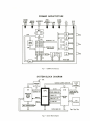
illustrates the general form of a system incorporating the COSMAC Microprocessor.
I
Design aids such as a Microprocessor hardware
support kit (COSMAC Microkit) and a program
development system with manuals and software
are provided to help system designers in the
development of Microprocessor-based products .
The following list summarizes the advanced fea tures and operating characteristics of t he COSMAC
Microprocessor :
• 8-bit parall el organization
• 8-bit bid irectional common bus for input/output
and memory
• stat ic COS/ MOS circuitry
• low power consumption
• single voltage option
• 4-12 Vdc operating range
• TTL compatibil ity
• high noise immunity
• singl e-phase clock
• singl e-pulse clear
• built-i n program load mode
• standard RAM/ ROM compatibil ity
• separate memory address lines
• direct memory addressing up to 65,536 bytes
• program interrupt mode
COSMAC provides a set of simple, easy-to -use,
general -purpose instructions. One can learn to
design programs for COSMAC-based products with
minimum effort . Unl imited subroutine nesting is
poss ible . The instruction set fac ilitates the use of
interpretive macro-instructions.The on-chip scratchpad of sixteen general -purpose 16-bit registers may
be used to provide multiple program counters, data
pointers, and data storage. Three specific registers
are treated by the hardware as implicit built-in DMA
add ress pointer, program counter for interrupt
servicing, and interrupt/subroutine stack pointer,
respectively . A simple one-step program load ing
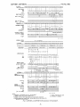
facility is provided on the chip. Fig. 1 shows the
internal structure of COSM AC.
• program controll ed interrupt mask (ena ble/
disable)
• self-contained DMA channel (cycl e st ealing mode )
• flexible progra mmed I/ O mode
• four I/O flag inputs directly testable by branch
instructions
• separate 4-bit I/ O control code
• two I/O sync pulses
• one-byte instruction format with two mach ine
cycles for each instruction
• 59 easy-to-use instructions
• multiple program counters
• multiple data regi st ers
• multipl e address regi sters
The COSMAC I/ O interface was designed to provide
direct control of I/ O devices so that over -all system
complexity and cost can be reduced. Flexible,
o pen-ended 110 instructions allow unlimited device
attachment. The hardware I/ O interface is capable
of supporting devices operating in polled , interrupt
driven, and Direct Memory Access modes. Fig. 2
• add, subtract, shift, and logical operat ions
• immediate address mode
• indirect pointer address mode
• fl ex ible subroutine nesting procedures
• branch and link capa bility
• same fetch and execute cycles for all inst ructions
2M l1 22A
Printed in U .S.A . 3/75
COSMAC ARCHITECTURE
TIMING
STATE
CODE
MREAD
MWRITE
M-ADDRESS
0-7
DMA
IN/OUT
INTERRUPT FLAGS
CLOCK
CLEAR
LOAD
3
2
N
BUS
0-7
0-3
3
(16)
VDD
R SELECT (4)
R(I).I R(I).O
VCC
R(2). 1 R(2).0
f-----lL----l_SCRATCH PAD
REGISTERS
VSS
8 - BIT BUS
Fig. 1 - COSMAC Architecture.
SYSTEM BLOCK DIAGR AM
.-
D
M
~
l
WI
CLOCK
a
CONTROL
«
N (4)
CPU
~",.
,
,
~-----"
I/O
t- -
-
-
- __ .J
TIMING a MSC.
DEPENDING ON
SYSTEM
STATE CODE (2)
TIMING (2)
COSMAC
,
U
BUS SEPARATOR
U
CLOCK,CLEAR,LOAD(3)
ADDRESS
LATCH
ADDRESS (8)
RAM/ROM
65536
BYTES
MAX.
TPA
MWRITE
DMA/INT. (3)
MREAD
FLAGS (4)
~
~
)
I/O
DEVICES
~ ~
)-
~.>
CONTROL
CKTS
DATA BUS (8)
Fig. 2 - System Block Diagram.
~
>
,
V DD , VSS ' VCC
Microprocessor Products
OO(]3LJ1]
Solid State
Division
CDP1801
CDP1801C
o
o
Ol
Q;
.0
E
:J
Z
!!!
u::
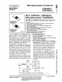
RCA CDP1801, CDP1801C
Microprocessor (COSMAC)
CDP180lU, CDP1801CU Microprocessor ControllC
CDP1801 R, CDP1801CR Microprocessor Register IC
Features:
CDP1801U,CU
4O-Lead Dual:rnLine Ceramic
(D)
H-1847
-
Static COS/MOS circuitry, no minimum clock frequency
Full military temperature range
High noise immunity, wide operating voltage range
TTL compatibility
S-bit parallel organization with bidirectional data bus
Built-in program-load facility
CDP1801 R,CR
Any combination of standard RAM/ROM
28.Lead Dual-In·
via common interface
Line Ceramic
H-1848
- Memory addressing up to 65,536 bytes
(D)
- Flexible programmed I/O mode
The RCA-COP1801 and COP1801 C Micropro- - Program interrupt mode
cessors (COSMAC) are LSI COS/MOS, 8-bit - On-chip OMA facility
register-oriented· central-processing units - Four I/O flag inputs directly testable by
(CPU) designed for use as general-purpose
Branch instructions
computing or control elements in a wide - One-byte instruction format with two machine
cycles for each instruction
range of stored-program systems or products.
The COP1801 and COP1801 C each comprise - 57 easy-to-use instructions
two units; the control unit designated COP- - 16 x 16 matrix of registers for use as multiple
1801 U, COP1801 CU and the register unit
program counters, data pointers, or data registers
designated COP1801 R, COP1801CR.
be realized. The COSMAC CPU also provides
The COP1801 is functionally identical to the
a synchronous interface to memories and exCOP1801 C. The COP1801 has an operating
ternal controllers for I/O devices and minivoltage range of 3 to 12 volts; the COP1801 C,
mizes the cost of interface controllers. Furan operating voltage range of 4 to 6 volts.
thermore, the I/O interface is capable of supporting devices operating in polled, interruptThese microprocessors include all of the cirdriven, or direct-memory-access modes.
cuits required for fetching, interpreting, and
executing instructions which have been stored
The COP1801 U and COP1801 CU control
in standard types of memories_ Extensive
units are supplied in a 40-lead hermetic ceinput/output (I/O) control features are also
ramic dual-in-line package (0 suffix) and in
provided to facilitate system design_
chip form (H suffix)_ The COP1801 Rand
COP1801 CR register units are supplied in a
The COSMAC architecture was designed with
28-lead hermetic ceramic dual-in-line package
emphasis on the total microcomputer system
(0 suffix) and in chip form (H suffix). For
as an integral entity so that systems having
ordering information, see dimensional outmaximum flexibility and minimum cost can
line page.
~==~~======~================~~>~~
Fig. I-COPIBOI, COPIBOIC Microprocessor data flow chart.
Trademarkls) Registered ® Information furnished by RCA is believed to be accurate and
rehab Ie. However, no responsibility is assumed by RCA for
Marea(s) Registrada(s)
its use; nor for any infringements of patents or other rights of
third parties which may result from its use. No license is
granted by implication or otherwise under any patent or
patent rights of RCA.
Printed in USA/9-75
File No. 900 _ _ _ _ _ _ _ _ _ _ _ _ _ __
CDP1801, CDP1801C
MAXIMUM RATINGS, Absolute-Maximum Values
Storage~Temperature
Range (T stg )
· .......................... -65 to +150 0 e
Operating~Temperature Range (T A)
· . . . . . . . . . . . . . . . . . . . . . . . . .. -55 to +125 0 C
DC Supply-Voltage Range (V ce ' VDDI
(All voltage values referenced to VSS terminal)
Vee';; V DD :
CDP1801 ................ 0.5 to +15 V
CDP1801e ..............
0.5to+7V
Power Dissipation Per Package (PO):
For T A = -55 to +100 0 e
................................. 500 mW
For TA = +100 to +125 0 e
· . . . . . . . . . . . . . . . .. Derate Linearly to 200 mW
Device Dissipation Per Output Transistor:
For TA = -55 0 e to +125 0 C ......... 100 mW
Input Voltage Range, All Inputs
· ...................... -0.5 to V DD +0.5 V
Lead Temperature (During Soldering):
At distance 1/16 ± 1/32 inch 11.59 ± 0.79 mml
from case for 10 5 max.
. ........... +265 o C
OPERATING CONDITIONS AT TA = 25°C Unless Otherwise Specified
For maximum reliability, nominal operating conditions should be
selected so that operation is always within the following ranges.
CONDITIONS
CHARACTERISTIC
Supply· Voltage Range
(At T A = Full PackageTemperature Range)
Recommended Input Voltage
LIMITS
CDP1801
CDP1801C
Max.
Min.
Min. Max.
VCC 1
(V)
VDD
(V)
-
-
3
12
4
6
V
VSS
VCC
V
15
/..IS
-
-
VSS
VCC
Clock Input Rise
or Fall Time, tr,tt
3·15
3·15
-
15
-
Instruction Time
(See Fig. 4)
5
5·10
5
10
16
6
-
16
-
-
-
-
5
5·10
5
5 - 10
5
5 - 10
5
5 - 10
5
10
5
DC
DC
1
3
DC
1
-
-
500
160
500
160
0
0
-
500
-
-
-
500
-
-
-
Clock Input Frequency, tCl
Clock Pulse Width, tWl' tWH
Clear Pulse Width
Data Hold Time, tDH
10
5
10
5
10
0
-
UNITS
/..IS
MHz
-
Notes:
1. vee';; V DD ' For CD1801e V DD
= Vee = 5 volts.
2. Because a large number of nodes may be switching simultaneously. a 0.1 }.J.F by·pass capacitor is
recommended in the power supply.
3. In order to maintain proper circuit operation, the CDP1801 intra~uni1 wiring capacitance should
be less than 25 pF.
-2-
ns
ns
ns
CDP1801, CDP1801C _ _ _ _ _ _ _ _ _ _ _ _ _ _ _ File No. 900
ELECTRICAL CHARACTERISTICS at T A = 25°C
CHARACTERISTIC
Static
Quiescent Device Current, I L
(See Figs. 11, 12)
CONDITIONS
CDP1801U,
CDP1801CU,
CDP1801R
CDP1801CR
VCCLIMITS
UNITS
LIMITS
Vo
VDD
(V)
(V)
Min. Typ. Max. Min. Typ. Max.
-
5
10
15
-
0.01
0.Q1
0.05
0.1
0.5
1.0
-
0.Q1
0.5
-
-
-
-
-
-
-
-
0
0.05
-
-
4.95
9.95
0
0
5
10
0.05
0.05
-
5
10
5
10
-
0.5
-1
4.5
9
5
10
5
10
1.5
3.0
1.5
3.0
1
1
4
9
5
10
5
10
0.4
0.5
2.5
4.6
9.5
5
10
5
5
10
mA
Output Voltage:
Low·Level, VOL
-
High·Level, VOH
-
-
4.95
5
-
-
-
2.25
3.45
2.25
3.45
-
1.5
2.25
-
-
-
1.5
2.25
1
1
1
1
-
-
1
-
-
-
1.6
3.6
-0.8
0
-0.45
3.2
7.2
-1.6
0
-0.9
-
1.6
-
-0.8
0
V
V
Noise Immunity:
Inputs Low, VNL
Inputs High, VNH
-
V
-
V
-
V
-
-
V
3.2
-
-
-1.6
0
-
-
-
-
-
1
-
-
-
Noise Margin:
Inputs Low, VNML
Inputs High, VNMH
Output Drive Current·:
N·Channel (Sink), ION
(See Figs. 7, 8)
P·Channel (Source), lOP
(See Figs. 5, 6)
Input Leakage Current
(Any Input). II L, II H
(See Figs. 13, 14)
-
-
-
-
-
±10- 5 ±1
-
5
-
-
-
-
-
15
-
±10- 5
±1
-
-
-
mA
mA
!lA
Dynamic at T A = 25°C, Input tr,tf = 20 ns, Cl = 50 pF
Propagation Delay Times:
(See Fig. 2)
Clock to TPA
tpAHL
Clock to TPB
.
5
10
-
685
240
-
-
685
-
-
-
720
250
430
190
650
230
-
720
-
-
-
-
5
10
5
10
5
10
-
-
5
10
-
900
340
-
-
900
tpMIHL
-
-
-
5
10
-
870
300
-
-
870
-
tpMOLH
-
-
-
-
-
tpALH
-
tpBHL
-
tpBLH
Clock-to-Memory Address
MA8toMA15
MAO to MA7
-
• Values are for signal lines going to external connections.
- 3-
-
-
-
-
430
-
650
-
-
ns
ns
ns
ns
ns
ns
File No. 900
~
_ _ _ _ _ _ _ _ _ _ _ _ _ CDP1801, CDP1801C
ELECTRICAL CHARACTERISTICS at TA = 25°C (CONT'D)
CHARACTERISTIC
Dynamic at T A = 25°C. Input tr.tt
CONDITIONS
CDP1801U,
CDP1801CU.
CDP1801CR
CDP1801R
VCC=
LIMITS
LIMITS
UNITS
Va
VDD
(V)
(V)
Min. Typ. Max. Min.1 Typ. Max
= 20 ns. Cl = 50 pF
Data Setup Time:
(See Fig. 2)
tSUlH
tSUHl
Clock-to-Memory Write Time
(See Fig. 2)
tpMWHl
tpMWlH
10
-
450
-
-
5
-
780
-
10
-
270
-
5
-
3
-
10
-
32
5
10
5
10
Any Input
-
170
100
30
20
5
-
5
750
-
ns
-
-
ns
-
3
-
-
-
-
-
170
-
-
-
-
-
-
-
30
-
-
ns
5
-
pF
-
750
-
-
-
-
780
-
-
-
Device Dissipation
(Total. Both Units). PD
I tCl = 1.0 MHz
I tCl = 3.0 MHz
OP CODE
= 00
Transition Time·:
(See Figs. 9, 10)
-
tTlH
tTHl
Input Capacitance, CI
-
-
-
• Values are for signal lines going to external connections.
DATA TO
MWR
cos MAC
1 PMWLH
---l j:-
-
CWHL
92CM-27016
Notes:
1. This timing dmgram is used to show signal relationships only
and does not represent any specifiC machine cycle
2. All measurements are referenced to 50% point of the
wave!orms.
Fig. 2- Timing waveforms.
-4-
mW
ns
CDP1801, CDP1801C _ _ _ _ _ _ _ _ _ _ _ _ _ _ _ File No. 900
DMA TIMING:
TPA
TPB
~so~i
STATE
SIORS2QR53
DMA-IN/DMA-OUT*
OMA-IN ONLY
OFF
[aus*
INPUT BYTE'
11
11'+-[1--
lMWR
92CL - 26422
GENERAL TIMING:
I--T(NOTEI)
...-.j
CLOCK
INTERNAL
TIMING INTERVALS
MACHINE CYCLE ~':":"-L_-"CY-"C",L",E-"'_'--L--"CY-"C:=L=-E,,-'+"''---L_-"CY"C,,,LE,,-,,-'+,,2'-'--L-':":"-=-_
-.+.r'
,
c+--
I
j~'''jUI
r
5T
05T
MEMORY TIMING:
ADDRESS
AAI~AO
MEMORY OUTPUT
He
,
J )
u/%/ft/h,
TPA
MEMORY ACCESS
15161710 I, 12131.15161710 I, 12 h 1.1516171 0I, 121 31_15161710 I, 12131
UI
~
II
OUTPUT
INSTRUCTION TIMING:
I----SO~
SI"I=6/IXXX
I---OFF-
STATE/N
i-----so----l
ijQ-N3
~/l
INPUT BYTE
II
u
L
,
so OR 52 OR $3
I----0FF-==
=
I
SI· I =6/0XXX
SO OR 52 OR 53
-LL::
N VALID
/l
BUS
[ S"(I 0 61'TPBl"
"--'
I
I
I
II
I
I I
l~
I
BUS*
MWR
"VALID BYTE
-----NOTE :3
TPB
STATE/N
1
wp
w/~=t//ft////1.
~ALLOWABLE
INPUT
INSTRUCTION TIMING:
I
1
J-.
1
"VAllO BYTE
T\~TJtr!.~LERVALS
f--
AI _AD-+---
AI I+--AO
I
M READ
MWR (NOTE 2)
I
I
I
I
,T
(MAO TO MA 7)
J
r
BYTE OUT
92CL-26421RL
NOTES:
I. MINIMUM T DETERMINED BY Voo -- NO MAXIMUM T
* = SIGNAL GENERATED BY
2. MEMORY WRITE PULSE WIDTH (MWR) RI 1.5 T
.a. = INTERNAL TO COSMAC
3. MEMORY OUTPUT "OFF II INDICATES HIGH-IMPEDANCE CONDITION
4. SHADING INDICATES MDON'T CARE" OR INTERNAL DELAYS DEPENDING ON
VDD AND THE CLOCK SPEED.
Fig. 3-CDP1801 and CDP1801C Microprocessor timing diagram.
·5·
USER
File No. 900 _ _ _ _ _ _ _ _ _ _ _ _ _ _ _ CDP1801, CDP1801C
(Vosl-V
DRAIN-TO-SOURCE VOLTAGE
-15
-10
-5
92C5-27018
Fig. 4- Typical instruction time
system access time.
tf:
GATE-TO-SOURCE VOLTAGE
¥o
~f
ttF
-+
VS.
memory
Fig. 5- Typical output-P-channel drain
characteristics.
AMBIENT TEMPERATURE (T A)" 25°C
"E,
~
, ,ftc
tHtttti+t:~t
GATE-TO~-S~~~AGE '(VGSI,,'15 ~- ..
-'00
~GS)"-5V
a~ eo
-IOj:
~
1
eft
z
~ 60
~ 40
-~.,j
~
-15
"
MAXIMUM DISSIPATioN
PER OUTPUT DEVICE;IOOmW
i}20
o
5
10
15
DRAIN-TO-SOURCE VOLTAGE (VOs)-V
92C5-27020
92C5-270J9
Fig. 6-Minimum output-P-channel drain
characteristics.
AMBIEN T TEMPERATURE (TA 1= 25°C
i
50
GATE-TO-SOURCE VOLTAGE (VGS):15
~4O
~
I~
~
v
;!
,:~
10
o
MAXIMUM DISSIPATION
PER OUTPUT DEVICE'" 100 mW
5
10
,~
15
(Vosl-V
92C5-21021
"" k ,;', .....:..
I;'"
i.e
s
'~
-5V
DRAIN-TO-SOURCE VOLTAGE
:,!.,
:
!I
~
§20
,;lim:!;:
"f
,
10V
,0
: (TA '-25"C
I
I~
.
"
1",30
A:D~~~~C
~
J::H+i
oo
~
Fig. 7- Typical output·N~hannel drain
characteristics.
~
a
ls.u
lin:
1;1;,
!";:; §
I is,
40
10
100
LOAD CAPACITANCE (c L)- pF
92C5-27022
Fig. 9- Typical high·to·low level
Fig. 8-Minimum output-N-channel drain
transition time vs. load
capacitance.
characteristics.
·6-
CDP1801, CDP1801C _ _ _ _ _ _ _ _ _ _ _ _ _ _ _ File No. 900
1
VOOa
~500
~
~
::E 400
SfffiITsr
!
[';
z
0
i
~
300
200
~
'1
>
<I
....
1
... :..... ... .........
I
...
T i l ,...
>=
>=
....
Vee
I·· .••
;2; ••••••••
I.
H~:
AMBIENT TEMPERATURE (TA 1= 25"C
~
••••
••••
••••
....
I 1 ...·0"''''\r-;;-,~ ..
... i .. t ..;;~r'2J
...
I~~/
1
.< ••••
I'~
"
, 100 ... h .. vrp.PL;;,;[p! 1
V
·1< I····: r
:.·1
L2P:_L j-,2l~ • ....
>
~
~
.....
.
~
20
40
60
80
100
LOAD CAPACITANCE (el 1- pF
nCS-27023
Fig. 10- Tvpicallow·to·high level
transition time vs. load
capacitance.
TEST CIRCUITS
Voo
IL
3.
I·
38
37
,
28
27
2.
2
25
24
23
36
35
3.
22
33
32
10
12
13
I.
I.
"
15
21
•
31
30
2.
28
-
27
2.
10
20
I.
12
13
I.
14
15
18
17
25
2.
17
18
2'
20
22
21
Vss
Fig. 12-COPISO I R, COP ISO I CR quiescent
device current.
Vss
Fig. II-COPISOIU, COPISOICU quiescent
device current.
Voo
f"
3'
33
t.a
32
NOTE
MEASURE INPUTS
SEQUENTIALLY, TO
BOTH Voo AN 0 Vss
CONNECT ALL UNUSED
INPUTS TO EITHER
VDO OR Vss
'If
Vss
10
31
30
12
2.
13
28
Vss
14
15
I.
I.
17
18
20
Vss
NOTES
MEASURE INPUTS
SEQUENTIALLY, TO BOTH
Voo ANO Vss. CONNECT
ALL UNUSED INPUTS TO
EITHER VDO OR Vss
25
24
23
WHEN MEASURING INPUT
22
LEAKAGE ON PINS 2,3,4,5,
24,25,26 a 27, PI N 23 MUST
21
BE CONNECTED TO VOD
Vss
92CS- 27027
92CS-27026
Fig. 13-COPISOIU, COPISOICU input
Fig. 14-COP1S01R, COP1S0lCR input
leakage current.
leakage curren t.
·7·
File No. 900 _ _ _ _ _ _ _ _ _ _ _ _ _ _ _ CDP1801, CDP1801C
The following is a brief description of the
COSMAC microprocessor. For more detailed
information see the following publ ication:
"User Manual for the COSMAC Micropro·
cessor"-MPM·l01. A Hardware Kit, CDP18S001 including the CDP1801 Microprocessor and support logic is also available.
The RCA Microprocessor (COSMAC) is implemented by two COS/MOS chips. The RCA
CDP1801U and CDP1801CU, in a 40-lead
dual-in-line ceramic package, .each contain
the arithmetic logic unit (ALUl. control logic,
and various working registers. The RCA CDP1801 Rand CDP1801CR, in a 28-lead dualin-line ceramic package, each contain the
mUlti-purpose 16 x 16 register array, a buffer
register, associated controls, and an increment/decrement circuit associated with the
register array.
COSMAC is a static system; therefore, the
clock input frequency can be chosen to
interface with memories or I/O devices
having speeds that vary over a wide range.
Also, the input clock may be stopped indefinitely with?ut loss of information.
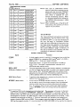
Architecture
The COSMAC block diagram is shown in
Fig. 15. The principal feature of this system
IS a register array (R) consisting of sixteen
16-bit scratchpad registers. Individual registers in the array (R) are designated (selected)
by a 4-bit binary code from one of the 4-bit
registers labeled N, P, and X. The contents
of any register can be directed to anyone of
the following three paths:
1. the external memory (multiplexed,
higher-order byte first, on to 8 memory address lines);
2. the D register (either of the two bytes
can be gated to D);
3. the increment/decrement circuit where
it is increased or decreased by one and
stored back in the selected 16-bit register.
The three paths, depending on the nature of
the instruction, may operate independently
or in various combinations in the same
machine cycle.
IIO FLAGS
I
MEMORY ADpRESS LINES
CONTROL LOGIC
(8)
(8)
CDP-180IR
COP-180IeR
CDP-180IU
CDP-180ICU
92CL-27028
81- DIRECTIONAL
BUS
Fig. 15-CDPIBOI, CDPIBOIC Microprocessor block diagram.
- 8-
CDP1801, CDP1801C _ _ _ _ _ _ _ _ _ _ _ _ _ _ _ File No. 900
Every COSMAC instruction consists of two
8·clock·pulse machine cycles. The first cycle
is the fetch cycle, and the second is the
execute cycle. During the fetch cycle the
four bits in the .p designator select one of
the 16 registers R (P) as the current program
counter. This selected R(P) contains the
address of the memory location from which
the instruction is to be fetched. When the
instruction is read out from the memory, the
higher·order 4 bits of the instruction byte
are loaded into the I register and the lower·
order 4 bits are fed to the N register. The
content of the program counter is auto·
matically incremented by one so that R (P)
is now "pointing" to the next byte in the
memory.
Data Pointers
The registers in R may be used as data
pointers to indicate where the data (operand)
is located in the memory. The register de·
signated by X [i.e., R(X)] points to the
operand for the following instructions (see
Table I):
1. ALU operations FO through F7;
2. output instructions 61 through 67;
3. input instructions 69 through 6F.
The register designated by N [i.e., R(N)]
points to the operand for the "load D from
memory" instruction 4N and the "store D"
instruction 5N. The register designated by P
(i.e., the program counter) is used as the data
pointer for ALU instructions F8 through FF.
During these instruction executions the oper·
ation is referred to as "data immediate".
Another important use of R as a data pointer
supports the built·in Direct·Memory·Access
(DMA) function. When a DMA·in or DMA·
out request is received, one machine cycle is
"stolen". This operation occurs at the end of
the execute machine cycle in the current
instruction. Register R (0) is always used as
the data pointer during the DMA operation.
The data is read from or written into the
memory location pointed to by the R (0)
register, whether the request is for "in" or
"out". At the end of the transfer, R(O) is
incremented by one so that the processor is
ready to act upon the next DMA byte trans·
fer request. Th is feature in the COSMAC
architecture saves a substantial amount of
logic when fast exchanges of blocks of data
are required, such as with magnetic discs or
during CRT·display·refresh cycles.
A program load facility, using this DMA
channel, is provided to enable users to load
programs into the memory. This facility pro·
vides a simple, one·step means for initially
entering programs into the microprocessor
system and eliminates the requirement for
specialized "bootstrap" ROM's.
Data Registers
The X designator selects one of the 16 reg·
isters R (X) to "point" to the memory for an
operand (or data) in certain ALU or I/O
operations.
The N designator can perform the following
five functions depending on the type of in·
struction fetched:
1. designate one of the 16 registers in R
to be acted upon during register opera·
tions;
2. indicate to the I/O devices a command
code or device·selection code for peri·
pherals.
3. indicate the specific operation to be
executed during the ALU instructions,
types of tests to be performed during
the Branch instructions, or operating
modes of interrupt handling instruc·
tions;
4. indicate the value to be loaded into P
to designate a new register to be used as
the program counter R(P);
5. indicate the value to be loaded into X
to designate a new register to be used as
data pointer R(X).
The registers in R can be assigned by a pro·
grammer in three different ways: as program
counters, as data pointers, or as scratch pad
locations (data registers) to hold two bytes
of data.
Program Counters
When registers in R are used to store bytes of
data, four instructions are provided which
allow D to receive from or write into either
the higher·order· or lower·order·byte por·
tions of the register designated by N. By this
mechanism (together with loading by data
immediate) program pointer and data pointer
designations are initiated. Also, this technique
allows scratch pad registers in R to be used to
hold general data.
Any register can be the main program
counter; the address of the selected register
is held in the Pdesignator. The other reg·
isters in R can be used as subroutine program
counters. By a single instruction the contents
of the P register can be changed to effect a
"call" to a subroutine. When interrupts are
being serviced, register R(1) is used as the
program counter for the interrupt servicing
routine. At all other times the register
designated as program counter is at the
discretion of the user.
Interrupt Servicing
Register R(1) is always used as the program
counter whenever interrupt servicing is ini·
tiated. When an interrupt request comes in
and the interrupt is allowed by the designer
·9·
File No. 900 _ _ _ _ _ _ _ _ _ _ _ _ _ _ _ CDP1801, CDP1801C
Interrupt Servicing - Cont'd
(again, nothing takes place until the end of
the current execute machine cycle of the
instruction is completed), the contents of the
X and P registers are stored in the temporary
register T, and X and P are set to new values;
hex digit 2 in X and hex digit 1 in P. Interrupt enable is automatically deactivated to
inhibit further interruptions. The interrupt
routine is now in control; the contents of T
are saved by means of a single instruction (78)
in the memory location pointed to by R(X),
where X = 2. At the conclusion of the interrupt, the routine restores the pre-interrupted values of X and P with a single instruction. The interrupt-enable flip-flop can
be activated to permit further interrupts or
can be disabled to prevent them.
COSMAC Register Summary
D
DF
8 Bits Data Register (Accumulator)
N
4 Bits Holds Low-order Instr. Digit
1 Bit
I
4 Bits Holds High-order Instr. Digit
Data Flag (ALU Carry)
R
16 Bits 1 of 16 Scratchpad Registers
T
P
4 Bits Designates which register is
Program Counter
B Bits Holds old X, P after Inter·
rupt (X is high byte)
IE
1 Bit
X
4 Bits Designates wh ich register is
Data Pointer
Interrupt Enable
Interrupt Action: X and P are stored in T
after executing current instruction; designator X is set to 2; designator P is set to
1; interrupt enable is reset to 0 (inhibit);
and instruction execution is resumed.
DMA Action: Finish executing current instruction; R(O) points to memory area
for data transfer; data is loaded into or
read out of memory; and increment R(O).
Note: In the event of concurrent DMA
and INTERRUPT requests, DMA has
priority:
-10 -
CDP1801, CDP1801C -
_ _ _ _ _ _ _ _ _ _ _ _ _ _ File No. 900
Instruction Set
Operation Notation
The COSMAC instruction summary is given
in Table 1. Hexadecimal notation is used to
refer to the 4·bit binary codes. Many of the
M(H(N))'" O;R(N) + 1
This notation means: The memory byte
pointed to by R(N) is loaded into 0, and
R(N) is incremented by 1.
instructions have been discussed in the Archi·
tecture section. Symbols used are:
R(W): Register designated by W, where
Slash (f) mark in Operations Column indicates
else or otherwise.
W = N, or X, or P
R(W).O: Lower·order byte of R(W)
R(W).1: Higher·order byte of R(W)
Table I - Instruction Summary
Register Operations
Code (Note 1)
Assembler Mnemonic (Note 2)
•
Name
Branching
,
rOPeration
I
'J"" Ii
r
r
-N
3 0
1 N INC INCREMENT R(N)+1
3 2
2 N DEC DECREMENT R(N)-1
R(N)'O+D
8 N GLO GET LO
9 N GHI GET HI
R(N).1+D
A N PLO PUT LO
D+R(N).O
B N PHI PUT HI
D+R(N).1
3 3
3 4
N=O, 1,2, ... ,9,A,B, ... ,E,F (Hexadecimal Notation)
UNCONO.BR. M(R(P))+R(P).O
M(R(PI)+R(P)O
BR.IF 0=00
IF O=OO/R (PI+1
M(R(P))+R(P).O
BOF BR.IF OF=l
IF DF=l/R(P)+l
BA.IF EF1=1 M(A(P))+R(PI.O
B1
IF EF1=1/RIP)+1
BR
BZ
3 5
B2
BR.IF EF2=1
3 6
B3
BR.IF EF3=1
3 7
B4
BR.IF EF4=1
SKP SKIP
Memory Reference
-I -N
4 N LOA iLOAD ADV
5 N STR [STORE
IM(R(N))+D;R(N)+1
I
3 8
ID+M(R(N))
I
3 A SNZ BR.IF D*OO
3 B BNF SR.IF DF=O
--
ALU Operations
I
R(P)+l
M(RIPII+R(P).O
IF D*OO/RIPI+1
M (R (P))+R(P).O
IF DF=O/R(P)+l
3 C BN1 BR.IF EF1=0 M(R(PI)+R(P).O
IF EF1=0/RIP)+1
N
F 0
M(R(P))+R(PI.O
IF EF2=1/R(P)+1
M(R(P))+R(P)O
IF EF3=1/R(PI+1
M(R(PI)+R(P).O
IF EF4=1/R(PI+1
LDX LOAD BY X
F 1 OR
OR
M(R(X))+D
3 D BN2 BR.I F EF2=0 M(R(PII+R(PI.O
IF Ef2=0/R(PI+1
M(R(X)) vD+D
F 2
AND AND
M(R(X))'D+D
F 3
XOR EXCl.OR
M(R(X))(i) D+D
F 4
AOD ADD
M(R(X))+D+D;C+DF
F 5
SO
F 6
SHR SHIFT
RIGHT
F 7
SM
SUBTRACT M O-M(R(X))+D,C+DF
F 8
LDI
LOAD IMM
SUBTRACT 0 M(RIX))-D+O,C+OF
SHIFT D RIGHT;
LSB+OF,O+MSB
Control
M(R(P))+D,R(P)+l
o
MIR(P))' D+P,R(P)+l
F B XRI EXCl.OR
IMM
M(R(P))(i) D+D;
RIP)+l
F D SOl
F F SMI
'I r;;
0
IDL IDLE
M (R(P)) vD+D,R(P)+l
F 9 ORI OR IMM
F A ANI AND IMM
F C ADI ADD IMM
3 E BN3 BA.IF EF3=0 M(R(PII+RIP)'O
IF EF3=0/R(PI+1
3 F BN4 SR.IF EF4=0 M(R(PII+R(P).O
IF EF4=0/R(PI+1
M(R(P))+D+D,
C+DF;R(P)+l
D N SEP SET P
N+P
E N SEX SET X
N+X
7 0
SUBT D IMM M(R(P))-D+D,
C+DF;R(P)+l
SUBTM IMM D-M(R(P))+D,
C+DF;R(P)+l
WAIT FOR
INTERRUPTI
DMA-INI
OMA-OUT
RET RETURN
7 1 DIS DISABLE
M(R(X))+<X, P;
R(X)+l;l+IE
M(R(X))~X,
R(XI+1;0+IE
7 8
SAV SAVE
'These are the only operations that modify
OF. OF is set or reset by an ALU carry
during add or subtract. Subtraction is by
2;s complement: A-B = A+B+1,
Note 1: The use of non-specified machine codes is not recommended .
. 11 .
T+M(R(X))
P;
File No. 900 _ _ _ _ _ _ _ _ _ _ _ _ _ _ _ CDP1801, CDP1801C
Input-Output Byte Tr.nlfor
7 'N
(Note 3)
6 1 OUT 1 OUTPUT 1 M(R(X))+BUS;
R(X)+I;N=1
6 2 OUT2 OUTPUT 2 M(R(X))+BUS;
!HX)+I;N=2
6 3 OUT3 OUTPUT 3 M(R(X))+BUS;
R(X)+I;N=3
6 4 OUT 4 OUTPUT 4 M(R(X))+BUS;
R(X)+I;N=4
6 5 OUT5 OUTPUT 5 M(R(X))+BUS;
R(X)+I;N=5
6 6 OUT 6 OUTPUT 6 M(R(X))+BUS;
R(X)+I;N=6
6 7 OUT7 OUTPUT 7 M(R(X))+BUS;
R(X)+I;N=7
6 9 INP 1
INPUT 1
6 A INP 2
INPUT 2
6 B INP3
INPUT3
6 C INP4
INPUT 4
6 D INP5
INPUT 5
6 E INP 6
INPUT 6
6 F INP 7
INPUT 7
BUS+M(R(X));
N=9
BUS+M(R(X));
N=A
BUS+M(R(X));
N=B
BUS+M(R(X));
N=C
BUS+M(R(X));
N=D
BUS+M(R(X));
N=E
BUS+M(R (X));
N=F
Note 2: Th is type of abbreviated nomenclature is used when programs are designed with the aid of the COSMAC
Assembler Simulator/Debugger System, which is available on commercial timesharing systems. Refer
to "Program Development Guide for
the COSMAC Microprocessor", MPM102, for details.
Note 3: When executing any of the 69 to 6F
instructions, the contents of the D
register may be altered.
Test and Branch
The Test and Branch instructions can branch
unconditionally, test for D=O or D=I, test
for DF=O or DF=I, or can test the status of
the four I/O flags. A "successful" branch
loads the byte following the instruction into
the lower-order byte position of the current
program counter, effecting a branch within
the current 256-byte "page" of memory. If
the test to branch is not successful, the next
instruction in sequence is executed.
SIGNAL DESCRIPTION
Function
Signal
A single negative pulse is required. A momentary low on this line
places COSMAC in a repeating IDLE cycle"'with P = 0, R(O) =
0000 and IE = 1 (interrupt request allowed).
CLOCK
Single-phase clock. A typical clock frequency is 2 MHz at
VDD = 10 V. The clock is counted down internally to 8
clock pulses per machine cycle.
MAO to MA7
(8 Memory Address Lines)
The most significant 8 bits of the memory address is multiplexed
out first on these lines and held in a latch in the memory system
that is set by TPA. The 8 least significant bits are then multiplexed out on the same lines. The memory system always sees
a 16-bit address within one memory-addressing cycle.
MWR (Write Pulse)
A positive pulse appearing in a memory-write cycle, after the
address lines have settled down.
M READ (Read Level)
A low level on M READ indicates a memory read cycle. It
can be used to control three-state outputs from the addressed
memory which may have a common data input and output
bus. If a memory does not have a three-state high-impedance
output, M READ is useful for driving memory/bus separator
gates.
'" A repeating IDLE cycle represents an instruction halt. The processor will remain in this halt
state until an I/O Request (INTERRUPT, DMA-IN, or DMA-OUT) is activated. When this
request occurs, the IDLE cycle is terminated and the I/O request is serviced, and then the normal program is resumed. If a DMA request is used to bring the processor out of IDLE, it will
increment the contents of R(O) by 1. The first instruction will, therefore, be fetched from
memory location 0001 and not 0000. Thus, program execution begins at location 0001 with
R(O) as the program counter. It is recommended that MEM.LOC.OOOO not be used by the program.
- 12-
CDP1801, CDP1801C _ _ _ _ _ _ _ _ _ _ _ _ _ _ _ File No. 900
The low M READ Iine enables the memory-out put-bus gates
during the read cycle (see Fig. 1, Timing Diagram).
BUSOto BUS 7
(Data Bus)
8·bit bidirectional DATA BUS lines. These lines are used for trans·
ferring data between the memory, the microprocessor, and I/O
devices.
NO to N3 (I/O Command)
Issued by an I/O instruction. They are interpreted by I/O controllogic to move data between the memory and the I/O interface (discussed in the Architecture section). These lines can be
used to issue command codes or device selection codes to the
I/O devices (independently or combined with the memory byte
on the data bus when an I/O instruction is executed). N bits are
set at the end of every SO cycle.
EF1 to EF4
(4 Flags)
These levels enable the I/O controllers to transfer status information to the processor. These levels can be tested by 'the conditional branch instructions. They can be used in conjunction
with the INTERRUPT request line to establish interrupt priorities. These flags can also be used by I/O devices to "call the
attention" of the processor, in which case the program must
routinely test the status of these flag(s). The flag(s) are set at the
end of every SO cycle.
INTERRUPT, DMA·IN,
DMA-OUT
(3 I/O requests)
These requests were discussed in the Architecture section. They
are sampled by COSMAC in the interval between the leading edge
of TPB and the leading edge of TPA. The DMA request has a
higher priority than the INTERRUPT request.
SCO,SC1,SC2
(3 State Code Lines)
These three lines indicate to the I/O controllers that the CPU is:
1 )processing a DMA request, 2)acknowledging an interrupt request,
3)fetching an instruction, 4)executing an I/O instruction, or 5)all
other instruction executions. The levels of state code are tabulated
below
State Code Li nes
State Type
SC2
SC1
SCO
S2 (DMA)
H
L
H
S3 (Interrupt)
H
L
L
SO (Fetch)
L
H
H
Sl
[1=6] (I/O Instruction Execute)
H
H
L
Sl
[1#6] (All other instructions)
H
H
H
All these states last one machine cycle. They may be assumed
valid at TPA. H = VCC, L = VSS'
TPA, TPB
(2 Timing Pulses)
Negative pulses that occur once in each machine cycle (TPB follows
TPA). They are used by I/O controllers to interpret codes and to
time interaction with the data bus. The trailing edge of TPA
is used by the memory system to latch the higher-order byte
of the 16-bit memory address.
LOAD
A low level that holds the CPU in IDLE mode and allows
an I/O device to load the memory without the need for a
"bootstrap" loader. It modifies the IDLE condition so that
DMA operation does not force execution of the next instruction.
VDD, VSS' VCC
(Power Levels)
The internal voltage supply VDD is isolated from the Input/
Output voltage supply VCC so that the processor may operate at maximum speed While interfacing with various external
circuit technologies, including T2L at 5 volts. Vee must be
less than or equal to VOO'
- 13-
File No. 900 _ _ _ _ _ _ _ _ _ _ _ _ _ _ CDP1801, CDP1801C
COSMAC Microprocessor State Transitions
Fig. 16 shows the CDP1801 and CDP1801C
Microprocessor state transitions. Each mao
chine cycle requires the same period of time8 clock cycles. The execution of each COSMAC instruction requires two machine cycles,
SO followed by Sl. S2 is the response
to a DMA request and S3 is the interrupt
response discussed in the preceding text.
Fig. 16-CDP/BOI, CDPIBOIC M,croprocessor
state transitions.
OPERATING AND HANDLING CONSIDERATIONS FOR CDP1801 MICROPROCESSOR
1. Handling
must be less than equal to V DD' Power
All inputs and outputs of this device have
supplies should be sequenced to insure
a network for electrostatic protection
compliance.
during handling. Recommended handInput Signals
ling practices for COS/MaS devices are
To prevent damage to the input protecdescribed in ICAN-6000 "Handling and
tion circuit, input signals should never be
Operating Considerations for MaS Ingreater than V DD nor less than VSS.
tegrated Circuits", available on request
Input currents must not exceed 10 mA
from RCA Solid State Division, Box 3200,
even when the power supply is off.
Somerville, N.J. 08876.
Unused Inputs
2. Operating
A connection must be provided at every
Operating Voltage
input
terminal.
All unused input terDuring operation near the maximum
minals must be connected to either VDD
supply voltage limit, care should be taken
or VSS, whichever is appropriate.
to avoid or suppress power supply turnon and turn-off transients, power supply
Output Short Circuits
ripple, or ground noise; any of these conShorting of outputs to V DD or VSS may
damage COS/MaS devices by exceeding
ditions must not cause VDD-VSS to
the maximum device dissipation.
exceed the absolute maximum rating. VCC
OPERATING AND HANDLING CONSIDERATIONS FOR CDP1801UH AND CDP1801 RH CHIPS
Mounting Considerations
B. Relative humidity, 50% max.
All COS/MaS chips are non-gold backed and
C. Clean, dust-free environment.
require the use of epoxy mounting. DuPont
2. The user must exercise proper care when
No. 5504A conductive silver paste or equivahandling chips to prevent even the slightest
lent recommended. In any case the manuphysical damage to the chip.
facturer's recommendations for storage and
3. During mounting and lead bonding of
use should be followed. If DuPont No. 5504A
chips
the user must use proper assembly
paste is used, the bond should be cured at
techniques to obtain proper electrical,
temperatures between 1850 C and 200 0 for
thermal, and mechanical performance.
75 minutes.
4. After the chip has been mounted and
In COS/MOS circuits P-channel substrates
bonded, any necessary procedure must be
are connected to V DD, therefore, when
followed by the user to insure that these
chips are mounted and a conductive paste is
non-hermetic chips are not subjected to
used care must be taken to keep the active
moist or contaminated atmosphere which
substrate isolated from ground or other
might cause the development of electrical
circuit elements.
conductive paths across the relatively
small insulating surfaces. In addition,
Packing, Shipping, and Storage Criteria
proper consideration must be given to
Solid·state 'chips, unlike packaged devices,
the
protection of these devices from
are non-hermetic devices, normally fragile
other harmful environments which could
and small in physical size, and therefore, reconceivably adversely affect their proper
quire special handling considerations as
performance.
follows:
These unmounted and unencapsulated chips
1. Chips must be stored under proper conditions to insure that they are not subare tested electrically and visually inspected
jected to a moist and/or contaminated
to meet RCA's specifications when they are
atmosphere that could alter their elec·
shipped by RCA. Written notification of
trical, physical, or mechanical characnon-conformance to such specifications must
teristics. After the shipping container is
be made to RCA within 90 days of the date
of the shipment by RCA. After shipment
opened, the chip mus1 be stored under
the following conditions:
from RCA, RCA assumes no responsibility
A. Storage temperature,. 400 C max.
for chips that have been subjected to further
- 14--
CDP1801, CDP1801C _ _ _ _ _ _ _ _ _ _ _ _ _ _ File No. 900
OPERATING AND HANDLING CONSIDERATIONS
FOR CDP1801 UH, CDP1801 RH CHIPS - CONT'D
For additional recommended handling prac·
processing, such as, but not limited to, lead
tices for COS/MaS chips, refer to ICAN-6000
bonding or chip mounting operations. RCA
reserves the right to change the chip design
"Handling and Operating Considerations for
and processing without notification.
MaS Integrated Circuits".
toCS-. . . . .
Dimensions and Pad Layout for CDP1S01UH Chip
92C5-27060
Dimensions and Pad Layout for CDP1801 RH Chip
Dimensions in parentheses are in millimeters and are
derived from the basic inch dimensions as indicated.
Grid graduations are in mils (10- 3 inch).
-15 -
File No. 900 _ _ _ _ _ _ _ _ _ _ _ _ _ _ _ CDP1801, CDP1801C
'1T:
. DB
-
{:~?~.
I.
2
!
L
31
30
12
13
2'
28
16
17
18
25
2.
23
MWR
19
22
VSS
20
21
DMA OUT
}
~
IIO
REQUEST
DMA IN
MEMORv-l
MA3
LINES
MA4
}CO~OL
}
M"REA'O
*
TOP VIEW
CDPtaOIU ,CDPl80lCU
~
ADDRESS
-
I.
_
BUSS
BUS7
} F~S
32
10
BUS
-
IIO
33
27
26
*
DATA{:~~~
3.
14
15
TPA
8US
35
N3
*
{CLOCK
TIMING{ fPB
PULSES
_
OATA
}
3.
COM~NOJ
_
3.
38
37
BUS I
BUSO
*
*
*
40
-
CODE
"no
27
26
25
BUS 2
BUS
2.
BUSI
-
BUSO
BUS 3} DATA
*
*
20
I. *
*
18
*
17
*
16
*CLEAR15
23
22
TPS-
21
10
MA5
STATE
28
MAS
12
MA7
13
Vss
14
TOP VIEW
CDPIBOIR ,COPIBOICR
92CS-26418RI
92CS-26417RI
Package Interconnections
Pin Terminals To:
• These pins are for interchip connections only.
Notes:
1. Any unused input pins should be connected to VDD or VCC.
2. The DATA BUS lines are bi·directional and have three·state outputs.
They may be individually connected to VCC through external pull-up
resistors (22 Knrecommended) to prevent floating inputs.
3. All inputs have the same noise immunity and level-shifing capability.
All outputs have the same drive capabil ity shether they have threestate outputs or not.
4. For the CDP1801 C, Vce must be connected to VDD.
Fig. 17- Terminal assignment diagrams.
DIMENSIONAL OUTLINES
CDP1801R, CDP1801CR
CDP1801U, CDP1801CU
28-Lead Ceramic
40·Lead Ceramic
DIM. MILLIMETERS
MIN.
35.06
2.16
MAX.
36.06
3.68
0.43
0.56
1.27 REF.
2.54 SSC
0.76
1.78
0.20
0.30
3.18
4.45
14.74 15.74
7'
1.27
0."
28
INCHES
MIN. MAX.
1.380
0.085
0.017
OIM.
1.420
0.145
A
0.023
0.050 REF.
0
F
0.100 esc
0.030 0.070
0.008
0.125
0.580
0.025
0.012
0.175
0.620
'"
0.050
28
M
MILLIMETERS
INCHES
MAX.
MIN.
50.30 51.30
2.42
3.93
0.43
0.56
1.27 REF.
2.54 sse
0.76
1.78
0.30
0.20
3.18
4.45
14.74 15.74
7'
1.27
0."
40
1.980
0.095
MIN.
MAX.
2.020
0.155
0.017 0.023
0.050 REF.
0.100 sse
0.030 0.070
0.008 0.012
0.125 0.175
0.580
0.620
0.025
0.050
'"
40
NOTES:
1. Leads within 0.13 mm {0.005) radius of true position
at maximum material condition.
2. Dimension "L" to center of leads when formed parallel.
3. When this device is supplied solder..ctipped, the maximum
lead thickness {narrow portion) will not exceed 0.013 in.
(0.33 mml.
ORDERING INFORMATION
The CDP1801 and CDP1801C are 2-package
microprocessors consisting of a control unit,
CDP1801U or CDP1801CU, and a register
unit, CDP1801 R or CDP1801CR.
When ordering both the control unit and the
register unit, request the CDP1801 or the
CDP1801 C. When ordering either the control
unit or the register unit, add the appropriate
RCAISolid State Division ISomerville, NJ 08876
suffix letter to the type number as follows:
Control Unit: CDP1801U, CDP1801CU
Register Unit: CDP1801R, CDP1801CR
When ordering a chip, add the suffix letter H
to the specific type number as follows:
Control Unit Chip: CDP1801 UH
Register Unit Chip: CDP1801 RH
When incorporating RCA Solid State Devices in
equipment, it is recommended that the designer
refer to "Operating Considerations for RCA Solid
State Devices", Form No, 1 CE-402, available on
request from RCA Solid State Division, Box 3200,
Somerville, N. J. 08876.
q§l
RCA Microprocessor Products
COSMAC Software Development Package
THE ASSEMBLER
The RCA symbolic assembly program (assembler)
is a computer program that assists the designer in
preparation of mach'ine code programs for the
RCA COSMAC microprocessor . The assembler
allows the system designer to write his program
(source program) in easy-to -remember symbolics.
The assembler converts these English -like mnemonics into machine-Iangauge binary words (object
program). It also does the tedious "book-keeping",
keeping track of cross references within the program,and facilitates the combining of subprograms
to form larger programs.
The assembler operates on a "one-for-one" basis,
in that each phrase of a statement in the source
program translates directly into a specific machinelanguage byte in the object program . The designer
thus has complete control over the object program
generated, but with maximum convenience and
readability.
Using the RCA assembler offers the following
advantages :
1. Fewer mistakes - because mnemonics are
provided for each instruction, and because
writing within a simple syntax reduces errors.
2. Easy program revision - because memory
locations and register names are designerassigned mnemonics, which do not change
when new instructions are inserted or old
ones deleted .
3. Easy understandability, both by the designer
and later by others - because of the mne monics used and because of the opportun ity
to add documentation comments at will. The
assembler will ignore these comments in the
process of assembling the source program .
The RCA assembly program provides two levels of
sophistication . At the first level, each instruction
is referred to by name , and each statement defines
a single instruction . The mnemonics of this level
are similar to other conventional assemblers, and
are the easiest for programming novices to learn.
The second level of the language provides a variety
of shorthand symbolics, some Fortran -like features,
and greater flexibility .
T~e assembler is written in standard Fortran IV,
to make it easy to install on a variety of computers.
THE SIMULATOR/ DEBUGGER
The COSMAC simulator/debugger enables the
designer to check out his program on timesharing
systems, using a variety of powerful debugging
tools. Fig . 1 shows the inter-relationship of the
assembler and simulator/debugger in the RCA
software support system .
H
L-____~
COSMAC
L_
M_IC_
R~_I_T~
Fig. 1 - RCA Software Support System.
To use the support system, the program designer
works at a terminal to prepare his source program,
using the editor, and then calls on the assembler
to assemble the program . After assembly, the prepared code is entered into the memory of the
simulated COSMAC system . During simulation the
user can stop the program at specified points or by
specified events . He can ask for the contents of
registers and memory locations using his original
assembly mnemonics, and change the values at will.
He can ask for traces - - blow-by-blow descriptions
of program execution . He can ask the simulator to
monitor specified locations and stop when they
are read, written to, or executed from. At any
time he can store away the entire state of the
simulated machine for later retrieval - - a particularly useful tool during debugging sessions, or
to avoid the cost of reassembly. When satisfied, the
user loads the program directly into his microprocessor hardware through his terminal , which
acts as an input device to the microprocessor . Final
verification of the program can now be done in
real time on the Microprocessor Hardware Support
Kit (COSMAC Microkit) .
(Over)
2Ml122B
Printed in U.S.A. 3/75
SOFTWARE SUPPORT SYSTEM AVAILABILITY
The software support system is available in two
forms . It has been installed on the General Electric
Information Services International Network for
use by timesharing customers. It is also available
f,rom RCA as a Fortran IV tape for installation on
any appropriate interactive computer. In this case,
it is supplied as a 9-track, BOO bpi IBM compatibletape, with a detailed installation manual.
[i)~
~
RCA Microprocessor Products
. _ -
----------------
-------------------------
RCA Microprocessor Hardware Support Kit
The RCA Microprocessor Hardware Support Kit
(COSMAC Microkit) is a prototyping system for
the development of systems based on the RCA
COSMAC Microprocessor. A Teletype*, or a termi nal with a TTL bit-serial interface, can be attached
to this system_ With such a terminal , it is an
elementary but complete computer system_ The
user is expected to provide something additional
to achieve his goals - - software, I/O device con troller, and perhaps additional memory.
In the basic configuration , the Microk it provides
the following :
1. 19" rack-mountable card nest, with printed circu it backplane
2. Self-contained power supply
3 . Front panel with basic controls
4 . Eleven 4.5" x 3.0" 44 -pin PC cards :
~onfiguring
the system to his particular requirements. A total of nine spare memory PC card
positions are pre bussed for memory expansion and
a total of fourteen spare I/O PC card positions
(one prewired) are made available for user device
control electronics.
Small 44-pin PC cards,
4 .5" x 3" are used in the basic Microkit card-set
for modularity and flex ibility in bu ild ing new
systems . Larger cards up to 4 .5" x 6.5", can be
used in the enclosure , if desired . The power supply
is capable of providing up to 2 amperes at 5 volts,
for additional cards .
Users may write and debug programs with the aid
of software packages available on timesharing
systems. The object code for a program may be
automatically loaded into the Microk it RAM for
further debugging.
The Microkit is designed for easy reconfigurability
and hardware extension, as well as for easy interaction with a timesharing system in software
development .
CPU card
Clock and Control
Bus Separato (2)
Address Latch Card
512-byte RAM Cards (2)
512-byte PROM Card
I/ O Decoder Card
Terminal Card (for Teletype*, or
Execuport**, etc .)
Byte I/ O Card
The Microkit is provided with a detailed manual ,
which carefully describes the hardware and the
Utility Program, and discusses generally the problems of designing a Microprocessor-based system.
Numerous examples are provided.
A block diagram of the Microkit is shown in Fig. 2.
Each block represents one card.
The 512-byte PROM card conta ins the Util ity Program , which performs commonly required functions :
program loading, memory dump, modification of
memory locations, paper tape punch , saving of
registers, and start of program execution at a
given location .
The Microkit has been designed to allow the user
to add memory cards and device electronics for
A photograph of the Microkit is shown in Fig. 1.
* Registered trademark of Teletype Corporation
**
.
Registered trademark of Computer Transceiver
Systems Inc.
Fig. 1 - COSMAC Microki t.
2Ml122C
Printed in U .S.A . 3/7 5
CONTROL SWITCHES
RAM I ROM SELECT
"
H ADDRS
I/O COMM AND
11':--,-,==-1
~~~~~
L ADDRS
STATE CODE
MEM. ADDRS
TPA
110
f-,N
"""'-L""IN
-:-:E:-:S,.-"-IDECODERf----------,
COS MAC
CPU
MWR
~g~:O I
'Vt- ---- ;t- --- --
r-
'r•
~ ---- ~
I
I
L ___ J
DATA
TO MEM.
S~~% RATOR
~
~
EFL AGS
DMA REO INTR REO
~~
MRE=AD~,~rJr----,++-----_+~---,II~~,l~Qn
RAM
MEMORY
RO M
ME MORyl
TPB
DATA
- - - - - - FRO M MEM
<"J.
DATA
TO DEV
f -_ _B::..;I.;;.DI;c.R..:;EC.:;..T--,I.;;.O__
NA_L::..;..:;D_AT_A---"
B,;;,U,;;,S_-i
S~~~RATOR
~
MEM WRITE
---=:; ----- -".j
~
BYTE
OATA
110
FROM DEV
~
T~~~~AL
(:=:
FACE
~
I
'-L ATCH
OUTPUT
S BITS
Fig. 2 - Microkit Block Diagram.
~
I ';SBIT
L-.J INPUT
I
I
~
I
USER
DE VICES
I
I
I
I
L _______ ~
User Manual For The
COSMAC Microprocessor (MPM-101)
The RCA Microprocessor Manual provides a detailed guide to the COSMAC Microprocessor . It is
written for the electrical engineer with no assumptions of familiarity with computers . It describes the microprocessor architecture and its
set of simple , easy -to-use instructions . Examples
are given to illustrate the operation of each
instruction .
The latter include Direct-Memory-Access and inter rupt inputs, external flag inputs, command lines,
processor state indicators, external timing pulses, etc.
This manual also gives a description of machinecode programming methods . Deta iled examples are
provided . Potential programming errors are discussed . Programming techniques regarding interrupt response, long branch, subroutine linkage
and nesting , and various programming techniques,
are also described.
For system designers, this manual illustrates practical methods of adding external memory and con trol circuits . Since the processor is capable of
supporting Input/ Output (I /O) devices in polled ,
interrupt-driven, and Direct-Memory-Access modes,
detailed examples are provided for the I/O instructions and the use of the I/O interface lines .
This basic manual is intended to help the design
engineer understand the COSMAC Microprocessor
and aid him in developing simpler and more
powerful products based on Microprocessors .
Microprocessor
Products
U.er Menue. for the
COSMAC Microproce ..or
ncn
....
r--
SOlid
State
I
I
MPM 101
2Ml122D
Pri nted in U.S .A . 3/75
Program Development Guide For The
COSMAC Microprocessor (MPM-102)
The Program Development Gu ide is a comprehen sive manual to be used with the COSMAC Software
Development Package for designing application
programs. First, it reviews the architecture of the
COSMAC Microprocessor so that program designers
can become familiar with its register set and
instruction repertoire, and with other functions
such as reset, load, start, DMA , and interrupt.
The manual then describes the COSMAC Software
Development Package (CSDP). CSDP is an interactive program which is available via nationwide
timesharing services or can be installed on a
customer's own interactive computer system.
needed . Blanks can be used at will to improve
readability . Comments can be inserted on any
line. The program is self documenting and
multiple instructions per line are permitted.
At the first level (Level I). each instruction is
referred to by name, and each statement defines a
single instruction. The mnemonics of this level
are similar to those of other conventional assem blers, and are the easiest for programming novices
to learn .
The second level (Level II) provides a variety of
shorthand symbolics, some Fortran -like features,
and greater flexibility .
It allows additional
mnemonics for some instructions, a wider use of
symbolic names than Level I, the use of expressions
to specify locations and values, etc . Level II is
thus a "higher-level" assembly language .
The COSMAC assembly language provides the
programmer with a means of writing and modifying
programs using convenient mnemonics. It has
been designed to provide the designer with com plete control over the object program generated,
but with maximum convenience and readability .
The format is free form ; no column lineup is
Several useful programming techniques, common
programming bugs, and sample programs are
discussed .
Microprocessor
Products
Program Development Guide
for the COSMAC Microproce •• or
ncn
MPM·l02
SOlid
State
I
~
-
I
$10,00 &.I.-lid PrIce
2M1122E
Pr inted in U .S.A. 3175