1
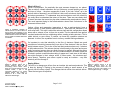
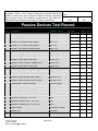
Component Testing Technical Manual Introduction: Digital multimeters can test a variety of electronic components. That’s primarily what they’re used for. Any technician worth their salt knows how to use a meter to test suspect components and troubleshoot electronic circuits. It’s important to note that this exercise is a continuation of the Digital Multimeter exercise found in the Tool Use and ID module. You might want to review it. In this lesson you’ll discover the true versatility of the Digital Multimeter and acquire some very important troubleshooting skills. Please remember that all meters are not the same. Some do not perform all test operations. The instructions listed below will work with any digital multimeter providing the meter has a continuity and resistance function setting. Your goal is to test the components in your electronic experimenter’s parts kit. You’ll not only become more familiar with your multimeter, you’ll also insure that you have all your parts and that they’re in good working order. Study the test procedures as outlined below and then print and complete the exercises. Words and Terms You Should Learn: Continuity Open Circuit Short Circuit Terminal Wiper Polarity Electrolytic Electrostatic Charge Coefficient Momentary Contact PN Junction Anode Cathode Emitter Base Collector Pin-Out Forward Bias Reverse Bias Gate Trigger Hold Doping Testing Passive Devices Passive devices are electronic components that provide no electronic gain or control. They don’t amplify, rectify or switch, but they do react to voltage and current. Wires, resistors, capacitors, coils, and switches fall into this category. Although passive devices are the least likely to malfunction, you should be able to test them if they’re suspect. The following panels will show you step-by-step procedures for testing the most common passive devices. Jumper Wire Test Procedure 1. 2. 3. Meter Setup Connect the test probes to the meter. Setup the meter. Connect the test leads to opposite ends of each jumper wire. Function: Continuity Range: Test Device Auto Min Max: Off Hold: Off Hz: Off Indication GOOD Beeper turns on direct continuity. BAD Beeper will not turn on and the resistance will read greater than 20 Ohms or indicate OL. indicating Schematic Application Notes: The continuity function works best as a fast convenient method to check for open circuits and shorts. The continuity check tests for resistances <20 Ohms. Component Testing Revised 11/7/2003 Frank C. Pendzich 8 July, 2002 Page 1 of 15 Battery Snap Meter Setup Test Procedure 1. 2. 3. 4. Test Device Connect the test probes to the meter. Setup the meter. Connect the test leads between the large connector and the end of the red wire on the battery snap. Connect the test leads between the small connector and the end of the black wire on the battery snap. Function: Continuity Range: Indication GOOD Beeper turns on indicating direct continuity for each wire. BAD Beeper will not turn on and the resistance will read greater than 20 Ohms or indicate OL. Auto Min Max: Off Hold: Off Hz: Off Application Notes: It may also be prudent to test if the battery snap is shorted. Connect the test leads to the ends of the red and black wires with no battery installed on the battery snap. There should be no continuity (OL) between the two wires. If the meter beeps then the battery snap is shorted (defective). Resistor Test Procedure 1. 2. 3. 4. Meter Setup Connect the test probes to the meter. Setup the meter. Connect the test leads across the resistor at the ends of the leads. Polarity isn’t important. Record the resistance indicated by the meter. Function: Indication GOOD The resistance indicated on the meter should match the ohmic value marked by the resistor’s color code. (± its tolerance rating) BAD The meter reading will not be within the resistor’s tolerance. Resistance Range: Auto Min Max: Off Hold: Off Hz: Off Schematic Application Notes: All resistors have a specific tolerance rating. The tolerance rating is marked by a color band on the very end of the resistor’s body. Normally the band is gold indicating 5% tolerance. If the tolerance band is silver, then the rating is 10%. If a 1000 Ohm resistor had a gold band for tolerance, the accuracy of the resistor would be 5% or ±50 Ohms. That means the resistor could measure anywhere between 950 and 1050 Ohms and still be good. Test Device Component Testing Revised 11/7/2003 Frank C. Pendzich 8 July, 2002 Page 2 of 15 1. 2. 3. 4. 5. 6. 7. Test Device Meter Setup Test Procedure Potentiometer Connect the test probes to the meter. Setup the meter. Connect the test leads to terminals 1 and 3 of the potentiometer. Polarity isn’t important. Record the resistance indicated by the meter. Connect the test leads to terminals 1 and 2 of the potentiometer. Polarity isn’t important. Observe the resistance as you rotate the potentiometer’s shaft. Record the min and max resistances. Function: Indication GOOD The meter should indicate the total resistance of the potentiometer. The resistance between terminals 1 and 2 should vary between 0 and the total resistance of the potentiometer. BAD A bad potentiometer will feel gritty as you turn the shaft. Also, the measured resistance won’t match the resistance rating of the potentiometer. Resistance Range: Auto Min Max: Off Hold: Off Hz: Off Schematic Application Notes: Most manufactures stamp the resistance of the potentiometer on the metal casing of its body. It’s usually pretty easy to find. If it’s not there, you can measure the potentiometer’s total resistance across terminals 1 and 3. Photocell Meter Setup Test Procedure 1. 2. 3. 4. Connect the test probes to the meter. Setup the meter. Connect the test leads across the photocell at the ends of the leads. Polarity isn’t important. Expose the top of the photocell to different levels of light. Test Device Function: Indication GOOD The measured resistance will change as the photocell is moved from bright to dim levels of light. BAD The measured resistance won’t change as you move the photocell from dark to light. Resistance Range: Auto Min Max: Off Hold: Off Hz: Off Schematic Application Notes: Photocells have a negative light coefficient meaning the photocells resistance drops as light level increases. Component Testing Revised 11/7/2003 Frank C. Pendzich 8 July, 2002 Page 3 of 15 Test Procedure Electrolytic Capacitor 1. 2. 3. 4. 5. 6. Test Device Meter Setup Connect the test probes to the meter. Setup the meter. Short out the leads to the capacitor for at least a second to discharge it. Connect the black test lead to the negative terminal of the capacitor. Connect the red test lead to the positive terminal of the capacitor. Observe what happens to the meter reading as the capacitor charges. Function: Indication GOOD On the capacitance setting, the measured value should approximately equal the value marked on the capacitor. Using the resistance setting, the measured resistance should start low and then steadily increase to infinite (OL). BAD The meter will not read the capacitance value marked on the side of the capacitor or will not charge if it’s defective. Capacitance Or Resistance Range: 20K Min Max: Off Hold: Off Hz: Off Schematic Application Notes: Some digital multimeters do not feature a capacitance function. You can however use the resistance setting to check to see if the capacitor is charging. Please note that some very large capacitors will take a long time to fully charge giving you an infinite or OL reading. Test Procedure Disc Capacitor 1. 2. 3. 4. 5. Test Device Meter Setup Connect the test probes to the meter. Setup the meter. Short out the leads to the capacitor for at least a second to discharge it. Connect the test leads across the disc capacitor at the ends of the leads. Polarity isn’t important. Observe what happens to the meter reading as the capacitor charges. Schematic Function: Indication GOOD On the capacitance setting, the measured value should approximately equal the value marked on the capacitor. Using the resistance setting, the measured resistance should read infinite (OL). BAD The meter will not read the capacitance value marked on the side of the capacitor or will not charge to infinity (OL) if it’s defective Capacitance Or Resistance Range: 2M Min Max: Off Hold: Off Hz: Off Application Notes: Ceramic disc capacitors are electrostatic devices meaning they are not polarized. You don’t have to take special polarity precautions when connecting the test leads to a disc capacitor. Some digital multimeters do not feature a capacitance function. You can however use the resistance setting to check to see if the capacitor is charging to infinity (OL). Since the capacitance of disc capacitors is so small this happens almost instantaneously. Component Testing Revised 11/7/2003 Frank C. Pendzich 8 July, 2002 Page 4 of 15 Loud Speaker Test Procedure 1. 2. 3. Meter Setup Connect the test probes to the meter. Setup the meter. Connect the test leads to the two terminals of the speaker. Function: Continuity Range: Indication GOOD Beeper turns on direct continuity. BAD Beeper will not turn on and the resistance will read greater than 20 Ohms or indicate OL. Auto Min Max: Off Hold: Off Hz: Off indicating Schematic Test Device Application Notes: Speakers are actually electromagnets. When you’re measuring across the two speaker terminals, you’re really measuring the conductivity of a coil. Since this speaker is relatively small, the resistance is so low that it can be measured with a continuity meter. Larger speakers would require you to use the resistance setting to check for shorts or opens in the speaker coil. PBNO Switch Test Procedure 1. 2. 3. 4. Meter Setup Connect the test probes to the meter. Setup the meter. Connect the test leads to the two terminals of the switch. Press the switch and observe the meter. Function: Indication GOOD Beeper turns on indicating direct continuity when the switch is pressed. BAD Beeper will not turn on and the resistance will read greater than 20 Ohms or indicate OL when the switch is pressed. Continuity Range: Auto Min Max: Off Hold: Off Hz: Off Schematic Test Device Application Notes: This particular switch is a normally open switch. That means that it will not let current flow through the switch when the button is not pressed because it is open. When the switch is pressed it becomes closed. Component Testing Revised 11/7/2003 Frank C. Pendzich 8 July, 2002 Page 5 of 15 Test Procedure Transistor Battery 1. 2. 3. 4. 5. 6. Test Device Schematic 7. Meter Setup Connect the test probes to the meter. Setup the meter. Connect the black test lead to the negative terminal of the battery. Connect the red test lead to the positive terminal of the battery. Record the measured voltage. While the test leads are connected, connect a 470 Ohm (Yellow, Violet, Brown) resistor to the positive and negative terminals to load the battery. Record the measured voltage. Indication Function: GOOD With the load resistor added, the voltage output of the battery should be within 80% of the rated value of the battery (9 vdc). BAD The battery is considered defective if the voltage output drops below 80% of the rated value of the battery. DC Volts Range: Auto Min Max: Off Hold: Off Hz: Off Application Notes: Even dead batteries will show their rated value on a meter if you don’t add a load resistance. The load resistance varies for each type of battery. D-Cell – RL = 10 Ohms, C-Cell – RL = 20 Ohms, AA-Cell – RL = 100 Ohms, and a 9-Volt Transistor Battery – RL = 330 Ohms. Testing Active Devices Discussion of Fundamentals: Active devices are semiconductors. It’s difficult to understand how semiconductors operate without diving into the murky depths of semiconductor theory. For now we’ll just splash around in the shallows. There are entire courses dedicated to teaching semiconductor operation and theory. This exercise will introduce you to some new terminology and cover the basic operating of the PN junction (diode). The idea is that you’ll grasp enough to understand how a meter can be used to test these important electronic devices. Basic Semiconductor Theory The electronic semiconductor industry has had a profound impact on our society. Semiconductors form the decision-making pathways of microprocessor chips and comprise the very building blocks of diodes and transistors. Anything that's computerized or uses radio waves depends on semiconductors to operate. Today, most semiconductor chips and transistors are created with silicon. Perhaps you’ve heard of "Silicon Valley" and the "silicon economy." These are just samples of the new terminology spawned by the high-tech industries that revolve around the silicon atom. Silicon is at the heart of any semiconductor device. Figure 1. IC Operational Amplifier, Transistor, and Light Emitting Diode The diode can be considered to be the simplest semiconductor device. It’s a good place to start if you want to know how semiconductors work. Component Testing Revised 11/7/2003 Frank C. Pendzich 8 July, 2002 Page 6 of 15 What is Silicon? Silicon is everywhere. It’s practically the most common element on our planet. Take a walk on a beach sometime and you’ll discover yourself strolling over tons and tons of silicon… the prime component of sand. If you look "silicon" up in the periodic table of elements, you will find that it sits next to aluminum, below carbon and above germanium. To understand how semiconductors work with electricity you really have to understand the nature of the atom. There are some basic rules of atomic structure that come into play when understanding semiconductor theory. The most important being is that semiconductor atoms want 8 electrons in the outermost electron shell. Figure 2. Crystalline structure of intrinsic silicon. In a silicon lattice, all silicon atoms bond perfectly to four neighbors, leaving no free electrons to conduct electric current. This makes a silicon crystal an insulator rather than a conductor. Carbon, silicon and germanium (germanium is also a semiconductor) have a unique property in their electron shell structure -- each has four electrons in its outer most orbit. This orbit is called the valence shell and this configuration allows atoms with a valence of four to form nice crystals. The four electrons form perfect covalent bonds with the four neighboring atoms, creating a lattice structure. This is called intrinsic or pure silicon. In carbon, we know this crystalline structure as diamond. In silicon, the crystalline form is a silvery, metallic-looking substance. Figure 3. Silicon and its neighboring elements on the Periodic Table. It’s important to note that electricity is the flow of electrons. Metals are good conductors of electricity because they have lots of "free electrons" that can move easily between atoms. This is due to the fact that conductors have only 1 electron in their valence orbits. The valence electron is held loosely to the atom and moves easily from atom to atom when any kind of energy is applied. Although the silicon crystals look metallic, they are not. All of the outer electrons in a silicon crystal are involved in perfect covalent bonds making it appear as if each atom in the lattice has eight electrons in their valence orbits. In other words… the electrons can't move around. Therefore, pure silicon crystal is nearly an insulator -- very little electricity will flow through it. Figure 4. P-Type - When gallium is added to intrinsic silicon, the 3 valence electrons bond to the surrounding silicon atoms. Since there isn’t enough electrons for all 4 covalent bonds, 1 pair is left incomplete resulting in an overall positive charge. This charge is referred to as a “hole” and the material is called P-Type. Component Testing Revised 11/7/2003 Frank C. Pendzich 8 July, 2002 Doping Silicon The trick is to change pure silicon from an insulator into and semiconductor. This is done by doping it. Doping is the process of adding a small amount of an impurity into the silicon crystal. This changes intrinsic silicon into extrinsic silicon. There are two types of impurities: Page 7 of 15 Figure 5. N-Type - When arsenic is added to intrinsic silicon, 4 of the valence electrons bond to the surrounding silicon atoms and one electron is left free. This results in an overall negative charge… or N-Type. • • N-type - In N-type doping, an element with a valence of 5 such as phosphorus or arsenic is added to the silicon in small quantities under intense heat and pressure. Since phosphorus and arsenic each have five valence electrons, when they’re added to the silicon, there will be one electron out of place when the impurity is merged into the silicon lattice. The fifth electron has nothing to bond to, so it's free to move around. It takes only a very small quantity of the impurity to create enough free electrons to allow an electric current to flow through the silicon. N-type silicon is a good conductor because if has lots of free electrons. Since electrons have a negative charge, the doped silicon is referred to as N-type. P-type - In P-type doping, boron or gallium is the dopant. Boron and gallium each have only three valence electrons. When mixed into the silicon crystalline structure, they form "holes" in the lattice where a silicon electron has nothing to bond to. The absence of an electron creates the effect of a positive charge, hence the name P-type. Holes can conduct current. A hole happily accepts an electron from a neighbor, moving the hole over a space. P-type silicon is a good conductor. A minute amount of either N-type or P-type doping turns a silicon crystal from a good insulator into a viable (but not great) conductor -- hence the name "semiconductor." N-type and P-type silicon are not all that amazing in and of themselves. However, when you put them together, you get some very interesting behavior at the PN junction. Creating a Diode Figure A Unbiased – Although there is no current applied to the diode, some of the free electrons in the N-type semiconductor cross the junction into the P-type material. This is caused by the attracting forces in the P-type material and is called diffusion. As electrons leave the N-Type to fill holes in the P-type some holes are created along the junction in the N-type semiconductor. Likewise, free electrons that border the junction in the P-type semiconductor. Just along the junction, all the free electrons in the N-type fill the holes in the P-type. The region is depleted of a carrier for current flow, so this area is referred to as the depletion region. In silicon it takes 0.7vdc of forward bias to breakdown this depletion region and force the diode to conduct. Component Testing Revised 11/7/2003 Frank C. Pendzich 8 July, 2002 Figure B Forward Biased – When the switch is closed, electrons from the negative terminal of the battery will stream into the N-type material. Moving through the N-type as if it were a conductor, the electrons combine with the holes and the PN junction and turn into valence electrons. This breaks down the depletion region (0.7 vdc – Silicon) essentially making it disappear. The electrons from the power source continue to fill all the holes in the P-type material. Once they are all filled, the remaining electrons become free to pass through the Ptype and continue on to the positive terminal of the battery. Current will flow when the diode is forward biased in this fashion. Page 8 of 15 Figure C Reverse Biased – Notice that the polarity of the power source has been reversed. When the switch is closed, the free electrons in the Ntype material are attracted to the positive terminal of the battery. The negative terminal of the battery injects electrons into the P-type semiconductor filling up the holes along the PN junction. The power source is essentially sucking all of the current carriers out of the diode, and in effect, increasing the size of the depletion region. Current cannot flow through a reverse biased diode because the depletion region is so large and there are no free electrons or hole to carry the current through it. A diode is the simplest of all semiconductor devices. A diode allows current to flow in one direction but not the other. You may have seen turnstiles at a stadium or a subway station that let people go through in only one direction. A diode is a one-way turnstile for electrons. When you put N-type and P-type silicon together, you get a very interesting phenomenon that gives a diode its unique properties (Figure A). In Figure B, the diode conducts electricity just fine. The free electrons in the N-type silicon are repelled by the negative terminal of the battery. The holes in the P-type silicon are repelled by the positive terminal. At the junction between the N-type and P-type silicon, holes and free electrons meet. The electrons fill the holes. Those holes and free electrons cease to exist, and new holes and electrons spring up to take their place. The effect is that current flows through the junction. Even though N-type silicon by itself is a conductor, and P-type silicon by itself is also a conductor, the combination shown in Figure C does not conduct any electricity. Flipping the battery around, the electrons in the N-type silicon get attracted to the positive terminal of the battery. The holes in the P-type silicon get attracted to the negative terminal of the battery. No current flows across the junction because the holes and the electrons are each moving in the wrong direction. Reverse biasing the diode in this way creates a region at the PN junction that’s depleted of holes or free electrons. Oddly enough… This is called the depletion region and current can’t pass through it because there’s nothing to carry it. A device that blocks current in one direction while letting current flow in another direction is called a diode. Diodes can be used in a number of ways. For example, a device that uses batteries often contains a diode that protects the device if you insert the batteries backward. The diode simply blocks any current from leaving the battery if it is reversed -- this protects the sensitive electronics in the device. Component Testing Revised 11/7/2003 Frank C. Pendzich 8 July, 2002 Page 9 of 15 Transistors and Chips A transistor is created by using three layers of semiconductor material rather than the two layers used in a diode. The two combinations you can create are either an NPN or a PNP sandwich. Transistors can act as either a switch or an amplifier. A transistor looks like two diodes back-to-back. You'd imagine that no current could flow through a transistor because back-to-back diodes would block current both ways. And this is true. However, when you apply a small current to the center layer of the sandwich, a much larger current can flow through the sandwich as a whole. This gives a transistor its switching behavior. A small current can turn a larger current on and off. A silicon chip is a piece of silicon that can hold thousands of transistors. With transistors acting as switches, you can create logic gates, and with logic gates you can create microprocessor chips. The natural progression from silicon to doped silicon to transistors to chips is what has made microprocessors and other electronic devices so inexpensive. These devices are so abundant in today's society and so powerful that tens of millions of transistors can be inexpensively formed onto a single chip. Test Procedure Diode 1. 2. 3. 4. 5. 6. 7. 8. Schematic Test Device N P Cathode Anode 9. Meter Setup Connect the test probes to the meter. Setup the meter. To Forward Bias the Diode Connect the black test lead to the cathode (C or the banded end) of the diode at the end of the lead. Connect the red test lead to the other (A or anode) end of the diode at the end of the lead. Record the reading. To Reverse Bias the Diode Reverse the leads so the red lead is connected to the cathode and the black lead is connected to the anode. Record the reading. Indication GOOD A good diode will show low resistance when it is forward biased and high resistance when it is reverse biased. BAD Open diodes will show high resistance in both forward and reverse biased conditions. Shorted diodes will indicate a low resistance in either state. There must be a significant difference in resistance between forward and reverse bias conditions. Function: Diode Or Resistance Range: KΩ Min Max: Off Hold: Off Hz: Off Application Notes: Some meters may require you to depress another switch to set the function to test diodes. Check with your meter’s user manual to be sure. For the diode to conduct electricity it must be forward biased. That means that the cathode must be negative and the anode positive. Component Testing Revised 11/7/2003 Frank C. Pendzich 8 July, 2002 Page 10 of 15 Light Emitting Diode (LED) 1. 2. 3. 4. 5. 6. 7. 8. Test Device N P Schematic Meter Setup Test Procedure 9. Connect the test probes to the meter. Setup the meter. To Forward Bias the LED Connect the black test lead to the cathode (C or the short lead) of the LED at the end of the lead. Connect the red test lead to the other (A or anode) end of the LED at the end of the lead. Record the reading. To Reverse Bias the LED Reverse the leads so the red lead is connected to the cathode and the black lead is connected to the anode. Record the reading. Function: Indication GOOD A good LED will show low resistance when it is forward biased and high resistance when it is reverse biased. BAD Open LEDs will show high resistance in both forward and reverse biased conditions. Shorted LEDs will indicate a low resistance in either state. There must be a significant difference in resistance between forward and reverse bias conditions. Diode Or Resistance Range: KΩ Min Max: Off Hold: Off Hz: Off Cathode Anode Application Notes: Some meters may require you to depress another switch to set the function to test diodes. Check with your meter’s user manual to be sure. For the LED to conduct electricity and light, it must be forward biased. That means that the cathode must be negative and the anode positive. Never… NEVER connect an LED directly to a battery to test it. You’ll burn it out in an instant. All LEDs must have a current limiting resistor in series with it before they’re connected to a power source. Component Testing Revised 11/7/2003 Frank C. Pendzich 8 July, 2002 Page 11 of 15 Test Procedure PNP Transistor (2N3906) 1. 2. 3. 4. 5. 6. 7. 8. 9. 10. 11. 12. 13. 14. 15. Test Device Collector Base Emitter P N P Schematic 16. Meter Setup Connect the test probes to the meter. Setup the meter. To Forward Bias the Base-Emitter Junction Connect the black test lead to the base (B) of the transistor at the end of the lead. Connect the red test lead to the emitter (E) at the end of the lead. Record the reading. To Reverse Bias the Base-Emitter Junction Reverse the leads so the red lead is connected to the base and the black lead is connected to the emitter. Record the reading. To Forward Bias the Base-Collector Junction Connect the black test lead to the base (B) of the transistor at the end of the lead. Connect the red test lead to the collector (C) at the end of the lead. Record the reading. To Reverse Bias the Base-Collector Junction Reverse the leads so the red lead is connected to the base and the black lead is connected to the emitter. Record the reading. Function: Indication GOOD When a transistor’s PN junctions are forward biased you should measure low resistance. When the PN junction is reverse biased the resistance will be high. BAD If the reverse resistance reading is low but not shorted, the transistor is leaky. If both forward and reverse readings are very high, the transistor is open. If the forward and reverse resistances are the same or nearly equal, the transistor is defective. A typical forward bias resistance is 100 to 500 ohms. However, a low power transistor might show only a few Ohms resistance when forward biased. Diode Or Resistance Range: KΩ Min Max: Off Hold: Off Hz: Off Application Notes: NPN and PNP transistors fall into the family of bipolar transistors and are easily tested with a multimeter. The transistor is basically and OFF device and must be turned on by applying forward bias to the emitterbase junction. Transistors are three-terminal devices that act like two diodes back-to-back. Each junction, like a diode should show low resistance with it’s forward biased and high resistance when it’s reverse biased. Important Note: Transistors come in a variety of case styles. The pin-out for the emitter, base, and collector is not the same from device to device. Likewise, it’s impossible to determine if a transistor is a PNP or NPN type by it’s shape or case design. Everything can be determined using the transistors part number. To get the right pin-out, you will have to refer to a semiconductor guide and look up the device using the part number. Another trick for common, low-power transistors, is to connect the ohmmeter to the collector and emitter, leaving the base hanging open. Apply polarity so the collector will be reverse biased (positive for NPN, negative for PNP.) Now wet a finger and thumb. Hold the base and collector leads in this finger/thumb clamp (don't let them touch). This injects some current into the base. If the ohmmeter resistance reading decreases, the transistor is working. By holding the base and emitter leads between thumb and finger, the resistance should go Up. These simple tests often tell if you have a PNP or NPN transistor, and if it is good or bad. Component Testing Revised 11/7/2003 Frank C. Pendzich 8 July, 2002 Page 12 of 15 Test Procedure NPN Transistor (2N3904) 1. 2. 3. 4. 5. 6. 7. 8. 9. 10. 11. 12. 13. 14. 15. Test Device Collector Base Emitter N P N Schematic 16. Meter Setup Connect the test probes to the meter. Setup the meter. To Forward Bias the Base-Emitter Junction Connect the red test lead to the base (B) of the transistor at the end of the lead. Connect the black test lead to the emitter (E) at the end of the lead. Record the reading. To Reverse Bias the Base-Emitter Junction Reverse the leads so the black lead is connected to the base and the red lead is connected to the emitter. Record the reading. To Forward Bias the Base-Collector Junction Connect the red test lead to the base (B) of the transistor at the end of the lead. Connect the black test lead to the collector (C) at the end of the lead. Record the reading. To Reverse Bias the Base-Collector Junction Reverse the leads so the black lead is connected to the base and the red lead is connected to the emitter. Record the reading. Function: Indication GOOD When a transistor’s PN junctions are forward biased you should measure low resistance. When the PN junction is reverse biased the resistance will be high. BAD If the reverse resistance reading is low but not shorted, the transistor is leaky. If both forward and reverse readings are very high, the transistor is open. If the forward and reverse resistances are the same or nearly equal, the transistor is defective. A typical forward bias resistance is 100 to 500 ohms. However, a low power transistor might show only a few Ohms resistance when forward biased. Diode Or Resistance Range: KΩ Min Max: Off Hold: Off Hz: Off Function: Application Notes: NPN and PNP transistors fall into the family of bipolar transistors and are easily tested with a multimeter. The transistor is basically and OFF device and must be turned on by applying forward bias to the emitter-base junction. Transistors are three-terminal devices that act like two diodes back-to-back. Each junction, like a diode should show low resistance with it’s forward biased and high resistance when it’s reverse biased. Important Note: Transistors come in a variety of case styles. The pin-out for the emitter, base, and collector is not the same from device to device. Likewise, it’s impossible to determine if a transistor is a PNP or NPN type by it’s shape or case design. Everything can be determined using the transistors part number. To get the right pin-out, you will have to refer to a semiconductor guide and look up the device using the part number. Another trick for common, low-power transistors, is to connect the ohmmeter to the collector and emitter, leaving the base hanging open. Apply polarity so the collector will be reverse biased (positive for NPN, negative for PNP.) Now wet a finger and thumb. Hold the base and collector leads in this finger/thumb clamp (don't let them touch). This injects some current into the base. If the ohmmeter resistance reading decreases, the transistor is working. By holding the base and emitter leads between thumb and finger, the resistance should go Up. These simple tests often tell if you have a PNP or NPN transistor, and if it is good or bad. Component Testing Revised 11/7/2003 Frank C. Pendzich 8 July, 2002 Page 13 of 15 Thyristor – SCR (S106B1) Test Procedure 1. 2. 3. 4. 5. 6. 7. 8. Test Device Schematic C Cathode N Gate P N Anode P 9. Meter Setup Connect the test probes to the meter. Setup the meter. Connect the black test lead to the SCR’s cathode (C). Connect the red test lead to the SCR’s Anode (A). Record the measured resistance. While the test leads are connected to the cathode and anode, slide the red test probe over so it is touching both the anode and gate leads at the same time. Do not remove the test probe from the SCR’s anode while doing this. Record the measured resistance. Slide the red test probe back over so it’s touching only the SCR’s anode. Record the measured resistance. Function: Indication GOOD Working SCRs will have high resistance until they are triggered by a positive voltage to the gate. Once triggered the resistance will be low and remain low even when the trigger voltage is removed. BAD An open SCR will not trigger when voltage is applied to the gate. Resistance will stay high. Shorted SCRs will have low resistance even when it hasn’t been triggered to conduct. Diode Or Resistance Range: KΩ Min Max: Off Hold: Off Hz: Off (K) G A Application Notes: An SCR is a gated diode that is used to control ac power. If a positive voltage is applied to the anode relative to the cathode, the diode will not conduct until it is triggered by current through the gate. Once triggered to on, the diode is turned off by an interruption in either cathode or anode current. Your really can’t test high current SCRs with an Ohmmeter because the current supplied by the multimeter may not be enough to fire or hold the SCR. The SCR tester circuit shown here will effectively test a variety of SCRs. This procedure will work with low current diodes though. Component Testing Revised 11/7/2003 Frank C. Pendzich 8 July, 2002 Page 14 of 15 Testing Integrated Circuits Test Procedure 555 IC Timer Test Device Schematic Meter Setup NOTE: The 555 Timer IC, like most integrated circuits cannot be tested with a multimeter. Although there is special test equipment designed to test a variety of IC chips, the equipment is simply too expensive for a small operation like a classroom. Perhaps the best way to test these devices is to test them in circuit. Many manufacturers of IC s publish specification sheets that include test circuits that a technician can build to test the integrated circuit. Simply build the circuit on a solderless circuit board and plug in the IC to test it. Function: N/A Range: N/A Min Max: N/A Hold: N/A Hz: N/A Indication GOOD The LEDs alternately about once per second. BAD • No LEDs flash. • Only one LED flashes. • Any LED is on or off all the time. flash Application Notes: Construction and Use Tips: The 555-tester shown here is basically a led flasher circuit but with the 555 removed. Imagine the output being a square-wave pulse with a high and low pulse, and is so indicated by the two LEDs, one 'Hi' and the other one 'Lo'. When you have a good 555 under test, the hi and lo LEDs are flashing steadily. If you have a defective 555 you may get both LEDs off, one or both on steady, or one or both on faintly. In all these cases the 555 is defective. Oh yeah, just in case you are just starting out in electronics; do NOT insert a 555 (or take it out) with the power on. The flash-rate can be changed with different values for C1 and R2. At pin 5 there is small ceramic 1nF capacitor. It is just there to filter out any noise. Experiment with leaving C2 out. C2 can be a value of 1nF to 10nF (0.001 to 0.01µF). In regards to R3, R4; depending on your LED type; start with 220 ohm and go up or down from 100 to 330 ohms, again, depending on your LED (regular, high, or ultra bright). Conclusions: Large things usually don’t work because their component parts have broken. The same is true for electronic appliances like computers. It’s not very often that you see a desktop computer burst into flames and burn down to ashes. Computers are made from thousands of individual electronic devices such as resistors, capacitors, transistors, and integrated circuits. When computer hardware malfunctions it’s usually because one of these smaller components has malfunctioned. Knowing how to identify these defective components is an integral part of being a computer service and support technician. Mastery of your digital multimeter will only make you a better technician. Component Testing Revised 11/7/2003 Frank C. Pendzich 8 July, 2002 Page 15 of 15 Component Testing Exercises 1 – Testing Passive Devices Exercise Objective: In this exercise you’ll test the passive devices that are found in your electronics experimenter parts kit. Passive devices seldom go bad. In fact, they’re typically the last thing you would suspect while troubleshooting. When passive devices such as resistors, capacitors, wires, and switches go bad… They go bad in a big way. It’s not uncommon to see them burnt or better yet blown to smithereens. Name: Period: Date: Nearly all defective passive devices can be identified by sight or smell. Never the less… Testing these components is good multimeter practice and will ease you into testing more complex active devices and integrated circuits. Discussion of Fundamentals: Most passive devices can be tested by measuring their resistance or continuity. The digital multimeter continuity function works best as a fast convenient method to check for open circuits and shorts. The continuity check tests for resistances less than20 Ohms. Even the battery snap can be tested measuring the continuity between the individual battery connectors and the ends of the wires. It may also be prudent to test the battery snap for shorts. Connect the test leads to the ends of the red and black wires with no battery installed on the battery snap. There should be no continuity (OL) between the two wires. If the meter beeps then the battery snap is shorted or defective. • All resistors have a specific tolerance rating. The tolerance rating is marked by a color band on the very end of the resistor’s body. Normally the band is gold indicating 5% tolerance. If the tolerance band is silver, then the rating is 10%. If a 1000 Ohm resistor had a gold band for tolerance, the accuracy of the resistor would be 5% or ±50 Ohms. That means the resistor could measure anywhere between 950 and 1050 Ohms and still be good. • Perhaps the most difficult step in testing a potentiometer is determining it’s Ohmic value. Most manufactures stamp the resistance of the potentiometer on the metal casing of its body. It’s usually pretty easy to find. If it’s not there, you can measure the potentiometer’s total resistance across terminals 1 and 3. Defective potentiometers will feel gritty when your turn the control shaft. This is normally due to carbon deposits from burning the resistance band or wiper contact. Photocells are light sensitive resistors. They have a negative light coefficient meaning the photocells resistance drops as light level increases. The easiest way to test this device is by measuring it’s resistance while moving it around to different light levels. If the resistance varies… it’s working. • Capacitors are also passive devices. Some digital multimeters do not feature a capacitance test function. You can however use the resistance setting to check to see if the capacitor is charging. Please note that some very large electrostatic capacitors will take a long time to fully charge giving you an infinite or OL reading. Ceramic disc capacitors are electrostatic devices meaning they are not polarized. You don’t have to take special polarity precautions when connecting the test leads to a disc capacitor. Since the capacitance of disc capacitors is so small this happens almost instantaneously. Component Testing Revised 11/7/2003 Frank C. Pendzich 8 July, 2002 Page 1 of 3 • Speakers are actually electromagnets. When you’re measuring across the two speaker terminals, you’re really measuring the conductivity of a coil. Since this speaker is relatively small, the resistance is so low that it can be measured with a continuity meter. Larger speakers would require you to use the resistance setting to check for shorts or opens in the speaker coil. • Switches can be tested using the continuity function on the digital multimeter. The electronics kit includes a PBNO switch. This particular switch is a normally open switch. That means that it will not let current flow through the switch when the button is not pressed because it is open. When the switch is pressed it becomes closed indicating direct continuity. • Measuring and testing batteries can be tricky. Even dead batteries will show their rated value on a meter if you don’t add a load resistance. The load resistance varies for each type of battery. D-Cell – RL = 10 Ohms, C-Cell – RL = 20 Ohms, AA-Cell – RL = 100 Ohms, and a 9-Volt Transistor Battery – RL = 330 Ohms. Load resistors are placed across the terminals of the battery while voltage is being measured. Research Resources: Company Acme How To Geofex Repair FAQ Incredible Batteries Intl. Electronics Online Fluke Meter NTE Inc. Web Site Description http://www.acmehowto.com/howto/homemaintenance/electrical/continuitytest.htm http://www.batteriesinternational.com/Issue 43 pdf's/43bat11.pdf Continuity Testing Tutorial Testing Resistors Capacitor Testing, Safe Discharging How I Fixed Multimedia Speakers Battery Technology Article http://www.electroline.com.au/elc/feature_story/092001.asp When You Buy a Digital Multimeter http://www.fluke.com/download/manuals/11x_____umeng0100.pdf Meter User Manual Electronic Component Distributor http://www.geofex.com/ampdbug/resistor.htm http://www.repairfaq.org/REPAIR/F_captest.html http://www.incredible.org.uk/geek/electronics/fix_speakers.html http://www.nteinc.com/ Required Materials: EKI Electronics Component Kit Discover Electronics! Manual Parts Kit Inventory Record Digital Multimeter Component Testing Revised 11/7/2003 Frank C. Pendzich 8 July, 2002 Page 2 of 3 Procedure: Test the following passive devices using a digital multimeter. Refer to the Testing Components Technical Manual for details on how to test each component. Mark all passing components that are good. Report any defective components to your supervisor. Record all of your results on the Passive Devices Test Record. Name Period Date Passive Devices Test Record Qty Description Standard Value 11 Wires, 4” Continuity 1 Battery Snap, 9V Continuity 1 Resistor, 10Ω (Brown, Black, Black) 10Ω ±5% 2 Resistor, 47Ω (Yellow, Violet, Black) 47Ω ±5% 2 Resistor, 100Ω (Brown, Black, Brown) 100Ω ±5% 2 Resistor, 220Ω (Red, Red, Brown) 220Ω ±5% 2 Resistor, 1KΩ (Brown, Black, Red) 1000Ω ±5% 1 Resistor, 2.2KΩ (Red, Red, Red) 2200Ω ±5% 1 Resistor, 3.3KΩ (Orange, Orange, Red) 3300Ω ±5% 1 Resistor, 6.8KΩ (Blue, Grey, Red) 6800Ω ±5% 1 Resistor, 16KΩ (Brown, Blue, Orange) 16000Ω ±5% 2 Resistor, 33KΩ (Orange, Orange, Orange) 33000Ω ±5% 1 Resistor, 120KΩ (Brown, Red, Yellow) 120000Ω ±5% 1 Resistor, 470KΩ (Yellow, Violet, Yellow) 470000Ω ±5% 1 Potentiometer, 100KΩ to 500KΩ 100K to 500KΩ 1 Photocell 3KΩ to 500KΩ 1 Capacitor, Electrolytic, 1000uF 16V 1000uF 1 Capacitor, Electrolytic, 100uF 25V 100uF 1 Capacitor, Electrolytic, 10uF 50V 10uF 1 Capacitor, Ceramic Disc, .1uF (104) .1uF 1 Capacitor, Ceramic Disc, .01uF (103) .01uF 1 Switch, PBNO Continuity (Closed) 1 Speaker, 8Ω Continuity 1 Battery, 9vdc 9vdc ±20% (Loaded) Component Testing Revised 11/7/2003 Frank C. Pendzich 8 July, 2002 Page 3 of 3 Measured Value Good Bad Component Testing Exercises 2 – Testing Active Devices Exercise Objective: In this exercise you’ll test the active devices that are found in your electronics experimenter kit. Active devices go bad all the time. In fact, they’re typically the first thing you would suspect while troubleshooting. When active devices such as diodes, LEDs, transistors, and thyristors go bad… Physical evidence is nearly impossible to detect. It’s not uncommon to see absolutely no sign of damage other than the fact that the darn thing doesn’t work. Name: Period: Date: Nearly all defective active devices require testing to determine a malfunction. The skills presented in this lesson are advanced multimeter testing techniques. Testing semiconductors is a vitally important skill to master. You’ll need these skills to troubleshoot computer power supplies or any device that uses diodes and transistors to operate. Testing Semiconductors • A single PN junction makes up a diode. A good diode will show low resistance when it is forward biased and high resistance when it is reverse biased. Open diodes will show high resistance in both forward and reverse biased conditions. Shorted diodes will indicate a low resistance in either state. There must be a significant difference in resistance between forward and reverse bias conditions. Some meters may require you to depress another switch to set the function to test diodes. Check with your meter’s user manual to be sure. For the diode to conduct electricity it must be forward biased. That means that the cathode must be negative and the anode positive. • LEDs operate in a similar fashion. For the LED to conduct electricity and light, it must be forward biased. That means that the cathode must be negative and the anode positive. Never… NEVER connect an LED directly to a battery to test it. You’ll burn it out in an instant. All LEDs must have a current limiting resistor in series with it before they’re connected to a power source. • NPN and PNP transistors fall into the family of bipolar transistors and are easily tested with a multimeter. The transistor is basically and OFF device and must be turned on by applying forward bias to the emitter-base junction. Transistors are three-terminal devices that act like two diodes back-toback. Each junction, like a diode should show low resistance with it’s forward biased and high resistance when it’s reverse biased. • Transistors come in a variety of case styles. The pin-out for the emitter, base, and collector is not the same from device to device. Likewise, it’s impossible to determine if a transistor is a PNP or NPN type by it’s shape or case design. Everything can be determined using the transistors part number. To get the right pin-out, you will have to refer to a semiconductor guide and look up the device using the part number. • Another trick for common, low-power transistors, is to connect the ohmmeter to the collector and emitter, leaving the base hanging open. Apply polarity so the collector will be reverse biased (positive for NPN, negative for PNP.) Now wet a finger and thumb. Hold the base and collector leads in this finger/thumb clamp (don't let them touch). This injects some current into the base. If the ohmmeter resistance reading decreases, the transistor is working. By holding the base and emitter leads between thumb and finger, the resistance should go Up. These simple tests often tell if you have a PNP or NPN transistor, and if it is good or bad. • Also known a thyristors, SCRs are also active devices. An SCR is a gated diode that is used to control ac power. If a positive voltage is applied to the anode relative to the cathode, the diode will not conduct until it is triggered by current through the gate. Once triggered to on, the diode is turned off by an Component Testing Revised 11/7/2003 Frank C. Pendzich 8 July, 2002 Page 1 of 2 interruption in either cathode or anode current. Your really can’t test high current SCRs with an Ohmmeter because the current supplied by the multimeter may not be enough to fire or hold the SCR. Research Resources: Company Electronix Express Integrated Publishing Anatekcorp Tony Van Roon Fluke Meter NTE Inc. Web Site Description http://www.elexp.com/t_test.htm http://www.tpub.com/neets/book16/67f.htm Diode and Transistor Testing Tutorial Testing Diodes Testing Transistors How I Fixed Multimedia Speakers Meter User Manual Electronic Component Distributor http://www.anatekcorp.com/qdmmvom.htm http://www.uoguelph.ca/~antoon/gadgets/scrtest.html http://www.fluke.com/download/manuals/11x_____umeng0100.pdf http://www.nteinc.com/ Required Materials: EKI Electronics Component Kit Discover Electronics! Manual Parts Kit Inventory Record Digital Multimeter Procedure: Test the following active devices using a digital multimeter. Refer to the Testing Components Technical Manual for details on how to test each component. Mark all passing components that are good. Report any defective components to your supervisor Name Period Date Active Devices Test Record Qty Description 1 Diode, 1N4003 Standard Value High Resistance Reversed Biased Low Resistance Forward Biased 1 LED, Red 5mm, 40 mA High Resistance Reversed Biased Low Resistance Forward Biased 1 Transistor, 2N3906, PNP Base–Emitter: High Resistance Reversed Biased Base–Emitter: Low Resistance Forward Biased Base–Collector: High Resistance Reversed Biased Base–Collector: Low Resistance Forward Biased 1 Transistor, 2N3904, NPN Base–Emitter: High Resistance Reversed Biased Base–Emitter: Low Resistance Forward Biased Base–Collector: High Resistance Reversed Biased Base–Collector: Low Resistance Forward Biased 1 SCR, SB106B1 Working SCRs will have high resistance until they are triggered by a positive voltage to the gate. Once triggered the resistance will be low and remain low even when the trigger voltage is removed. Component Testing Revised 11/7/2003 Frank C. Pendzich 8 July, 2002 Page 2 of 2 Ω Good Bad Component Testing Exercises 3 – Testing ICs Exercise Objective: In this exercise you’ll test the 555 Timer Integrated Circuit that’s part of your electronics kit. You’ll learn how to test IC devices using operational tests and how to recognize when an IC is defective. Name: Period: Date: Discussion of Fundamentals: When IC chips go bad, the only way to tell is they simply don’t work. There are few other signs. ICs go bad all the time. In fact, they’re the most frequent cause of system failures. It’s also important to note that chips themselves cannot be repaired. They’re just removed and replaced. The 555 Timer IC, like most integrated circuits, cannot be tested with a multimeter. Although there is special test equipment designed to test a variety of IC chips, the equipment is simply too expensive for a small operation like a classroom. Perhaps the best way to test these devices is to test them in circuit. Many manufacturers of IC s publish specification sheets that include test circuits that a technician can build to test the integrated circuit. Simply build the circuit on a solderless circuit board and plug in the IC to test it. The 555-tester shown here is basically a led flasher circuit but with the 555 removed. Imagine the output being a square-wave pulse with a high and low pulse, and is so indicated by the two LEDs. When you have a good 555 in the test circuit, the LEDs will flash steadily. If you have a defective 555 both LEDs may be off, flashing dimly, or both constantly on. In all of these cases the 555 is defective. Oh yeah, just in case you are just starting out in electronics; do NOT insert a 555 (or take it out) with the power on. Also make sure it is plugged in to the test circuit correctly. That means pin 1 to pin 1. Otherwise the chip will melt down. 555 Timer IC Pin-Out Test Circuit with IC Socket The flash-rate can be changed with different values for C1 and R2. C2 can be a value of 1nF to 10nF (0.001 to 0.01µF). In regards to R3; depending on your LED type; start with 220 ohm and go up or down from 100 to 330 ohms, again, depending on your LED (regular, high, or ultra bright). Component Testing Revised 11/7/2003 Frank C. Pendzich 8 July, 2002 Page 1 of 2 IC Test Circuit Schematic Research Resources: Company Tony Van Roon NTE Inc. NTE Inc. EKI Int. Web Site Description http://www.uoguelph.ca/~antoon/gadgets/555/555.html Testing 555 Timer IC Tutorial Electronic Component Distributor 555 Time Specification Sheet Starter Set – LED Blinker http://www.nteinc.com/ http://www.nteinc.com/specs/900to999/NTE955.html http://www.eki.com/product_info.asp?number=2000 Required Materials: EKI Electronics Component Kit LED Blinker Kit Procedure: Test the 555 Timer IC using the LED Blinker circuit. Refer to the Testing Components Technical Manual for details on how to test the component. Mark all passed tests as good. Report any defective tests to your supervisor Name Period Date 555 Timer IC Test Record Step Description Standard Value 1 Insert the 555 IC into the test circuit. Note: Pin 1 must be connected to pin 1. 2 Attach a good 9 Volt battery to the circuit. Note: Observer battery polarity. 3 Observe the LEDs Do the LEDs flash? 4 Are the LEDs bright? 5 Do the LEDs flash about 4 times / second? 6 Is the 555 Timer IC Good? Component Testing Revised 11/7/2003 Frank C. Pendzich 8 July, 2002 Page 2 of 2 Yes No