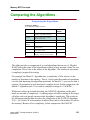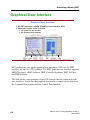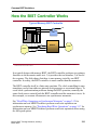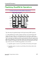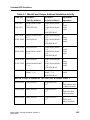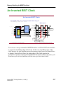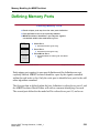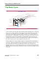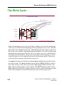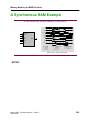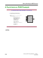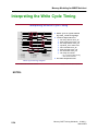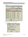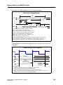
1
Memory BIST Training Workbook Software Version 8.2004_1 February 2004 Copyright Mentor Graphics Corporation 1999 - 2004. All rights reserved. This document contains information that is proprietary to Mentor Graphics Corporation. The original recipient of this document may duplicate this document in whole or in part for internal business purposes only, provided that this entire notice appears in all copies. In duplicating any part of this document, the recipient agrees to make every reasonable effort to prevent the unauthorized use and distribution of the proprietary information. End-User License Agreement This document is for information and instruction purposes. Mentor Graphics reserves the right to make changes in specifications and other information contained in this publication without prior notice, and the reader should, in all cases, consult Mentor Graphics to determine whether any changes have been made. The terms and conditions governing the sale and licensing of Mentor Graphics products are set forth in written agreements between Mentor Graphics and its customers. No representation or other affirmation of fact contained in this publication shall be deemed to be a warranty or give rise to any liability of Mentor Graphics whatsoever. MENTOR GRAPHICS MAKES NO WARRANTY OF ANY KIND WITH REGARD TO THIS MATERIAL INCLUDING, BUT NOT LIMITED TO, THE IMPLIED WARRANTIES OR MERCHANTABILITY AND FITNESS FOR A PARTICULAR PURPOSE. MENTOR GRAPHICS SHALL NOT BE LIABLE FOR ANY INCIDENTAL, INDIRECT, SPECIAL, OR CONSEQUENTIAL DAMAGES WHATSOEVER (INCLUDING BUT NOT LIMITED TO LOST PROFITS) ARISING OUT OF OR RELATED TO THIS PUBLICATION OR THE INFORMATION CONTAINED IN IT, EVEN IF MENTOR GRAPHICS CORPORATION HAS BEEN ADVISED OF THE POSSIBILITY OF SUCH DAMAGES. RESTRICTED RIGHTS LEGEND 03/97 U.S. Government Restricted Rights. The SOFTWARE and documentation have been developed entirely at private expense and are commercial computer software provided with restricted rights. Use, duplication or disclosure by the U.S. Government or a U.S. Government subcontractor is subject to the restrictions set forth in the license agreement provided with the software pursuant to DFARS 227.72023(a) or as set forth in subparagraph (c)(1) and (2) of the Commercial Computer Software - Restricted Rights clause at FAR 52.227-19, as applicable. Contractor/manufacturer is: Mentor Graphics Corporation 8005 S.W. Boeckman Road, Wilsonville, Oregon 97070-7777. This is an unpublished work of Mentor Graphics Corporation. Table of Contents Table of Contents About This Training Workbook............................................................................ix Introduction............................................................................................................ix Audience .................................................................................................................x Primary Audience.................................................................................................x Secondary Audience.............................................................................................x Course Timeline.....................................................................................................xi Course Overview ..................................................................................................xii Prerequisite Knowledge.......................................................................................xiii Acronyms Used in This Workbook .....................................................................xiii Customer Support Information ............................................................................xiv Module 1 Memory BIST Concepts .....................................................................................1-1 Objectives ............................................................................................................1-1 Embedded Memories ...........................................................................................1-2 Typical Architecture with Embedded Memories.................................................1-4 Types of Memories ..............................................................................................1-5 Types of Testing ..................................................................................................1-7 Functional Testing ...............................................................................................1-8 Direct Access Testing ..........................................................................................1-9 Memory BIST Testing .......................................................................................1-10 When Should You Use Memory BIST? ............................................................1-11 Advantages of Adding BIST .............................................................................1-13 Disadvantages of Adding BIST .........................................................................1-14 Inserting BIST Circuitry ....................................................................................1-16 Memory Testing and Fault Types......................................................................1-17 Stuck-at Faults ...................................................................................................1-19 Stuck-at Faults ..................................................................................................1-20 Transition Faults ................................................................................................1-21 Transition Faults (Continued) ...........................................................................1-22 Coupling Faults..................................................................................................1-23 Neighborhood Pattern Sensitive Faults .............................................................1-26 Testing for Cell Array Faults ............................................................................1-28 Memory BIST Algorithms.................................................................................1-30 Memory BIST Training Workbook, V8.2002_1 March 2002 iii Table of Contents Table of Contents (cont.) Comparing the Algorithms ................................................................................1-31 March C+ (March 2) .........................................................................................1-33 Module 2 Generating a Memory BIST...............................................................................2-1 Objectives ............................................................................................................2-1 Typical Memory BIST Flow ...............................................................................2-2 MBISTArchitect Inputs and Outputs...................................................................2-4 Graphical User Interface......................................................................................2-6 MBISTArchitect GUI Overview .........................................................................2-7 Role of the Test Bench ........................................................................................2-8 Memory BIST Documentation ............................................................................2-9 Module 2 Lab Exercises ....................................................................................2-10 Module 2: Lab Exercises ...................................................................................2-11 Getting Started ...................................................................................................2-11 Software Versions ...........................................................................................2-11 Training Files ..................................................................................................2-12 Installing the Training Data Files....................................................................2-12 Exercise 1: Creating a Basic Memory BIST Collar ...................................... 2-14 Exercise 2: Verifying the BIST Circuitry ..................................................... 2-20 Module 3 Common BIST Variations ...................................................................................3-1 Objectives ............................................................................................................3-1 Configuring Memory BIST Circuitry ..................................................................3-2 Support for Multi-port Memories ........................................................................3-5 Generate a Comparator Functional Test ..............................................................3-6 Inserting BIST for Multiple Memories................................................................3-8 MBISTArchitect Controller Options .................................................................3-10 How the BIST Controller Works .......................................................................3-11 Read/Write Operations on Synchronous Memories ..........................................3-12 Full-Speed Overview .........................................................................................3-14 Full-speed design with pipeline circuitry ..........................................................3-16 Pipelining Read/Write Operations .....................................................................3-17 iv Memory BIST Training Workbook, V8.2002_1 March 2002 Table of Contents Table of Contents (cont.) Performing Sequential Memory Tests ...............................................................3-19 Adding Diagnostics ...........................................................................................3-21 Clock Synchronization ....................................................................................3-23 Compressor vs. Comparator ..............................................................................3-25 BIST using a Compressor ..................................................................................3-27 Adding Pipeline Registers .................................................................................3-29 Specifying Non-controlled Memory Ports.........................................................3-32 Specifying Parameters for Memory Clock Signals ...........................................3-34 Bypassing Memory in Scan Mode.....................................................................3-35 Synthesis Driver File ......................................................................................3-38 Design Compiler Clock Constraints ..................................................................3-40 Mux-Embedded Memory Support .....................................................................3-41 Module 3 Lab Exercises ....................................................................................3-43 Module 3: Lab Exercises ...................................................................................3-44 Exercise 3: Changing the BIST Algorithm ................................................... 3-45 Exercise 4: Changing the Data Background ................................................. 3-49 Exercise 5: Inserting BIST for Multiple Memories ...................................... 3-51 Exercise 6: Adding BIST with a Compressor ............................................... 3-57 Exercise 7: Running BIST at Full-Speed ...................................................... 3-61 Extra Credit .....................................................................................................3-65 Test Your Knowledge .....................................................................................3-66 Lab Summary ..................................................................................................3-66 Exercise 8: Adding BIST for Bidirectional Memories ................................. 3-67 Exercise 9: Adding BIST for ROMs............................................................. 3-68 Module 4 Memory BIST-In-Place ........................................................................................4-1 Objectives ............................................................................................................4-1 Memory BIST-In-Place Flow ..............................................................................4-2 Memory BIST-In-Place Flow Overview .............................................................4-3 Creating BIST Structures.....................................................................................4-5 Model Creation ....................................................................................................4-6 Memory Model Example .....................................................................................4-7 Creating BIST Structures Invocation...................................................................4-8 Basic Command Flow..........................................................................................4-9 Memory BIST Training Workbook, V8.2002_1 March 2002 v Table of Contents Table of Contents (cont.) Creating BIST Structures Results ......................................................................4-10 Example of RTL BIST Logic ............................................................................4-11 Example WGL File............................................................................................4-12 Core Test Description File (CTDF) ...................................................................4-14 Connecting BIST Structures ..............................................................................4-17 Connecting BIST Structures Invocation ............................................................4-18 Example Command Flow (Setup) .....................................................................4-19 Example Continued (Setup)...............................................................................4-20 Example Command Flow (Synthesis) ...............................................................4-21 Connecting BIST Structures Results .................................................................4-22 Connecting BIST Structures Dofile...................................................................4-23 Example CTAF File...........................................................................................4-24 Example RTL Phase Decoder............................................................................4-25 Integrating BIST Patterns ..................................................................................4-26 Integrating BIST Patterns Invocation ................................................................4-27 Integrating BIST Patterns Commands ............................................................4-28 Continued Example (Integration) ......................................................................4-29 Integrating BIST Patterns Dofile .......................................................................4-30 Integrating BIST Patterns Results .....................................................................4-31 Verification ........................................................................................................4-32 I/O Pads .............................................................................................................4-33 Global Signal Connections ................................................................................4-34 BSDArchitect/ Memory BIST-In-Place Integration ..........................................4-35 Module 4: Lab Exercises ...................................................................................4-37 Exercise 10: Setting Up MBISTArchitect Outputs ....................................... 4-38 Exercise 11: Inserting BIST Controllers using Memory BIST-In-Place ...... 4-42 Exercise 12: Translating BIST Patterns to the SoC Level ............................ 4-45 Exercise 13: Full Flow Exercise ................................................................... 4-47 Module 5 Memory Modeling for MBISTArchitect ...................................................................................................5-1 Objectives ............................................................................................................5-1 A Memory Model: ...............................................................................................5-2 Memory Model Syntax .......................................................................................5-3 vi Memory BIST Training Workbook, V8.2002_1 March 2002 Table of Contents Table of Contents (cont.) Memory Model Editor .........................................................................................5-4 Loading Library Files and Models ......................................................................5-5 Defining Inputs/Outputs ......................................................................................5-7 The Dont_touch Keyword ...................................................................................5-9 Understanding Clocking Schemes .....................................................................5-10 Clock Connections.............................................................................................5-12 No Memory Clock .............................................................................................5-14 A Gated Memory Clock.....................................................................................5-15 A Non-Gated Memory Clock ............................................................................5-16 An Inverted BIST Clock ....................................................................................5-17 Test Clock ..........................................................................................................5-18 Control Retention Test Delay ............................................................................5-19 Memory Ports ....................................................................................................5-20 Defining Memory Ports .....................................................................................5-21 Port Definition Example 1 .................................................................................5-22 Port Definition Example 2 .................................................................................5-23 Read/Write Cycle Syntax ..................................................................................5-24 The Read Cycle..................................................................................................5-25 The Write Cycle.................................................................................................5-26 Interpreting Data Sheets ....................................................................................5-27 A Synchronous RAM Example .........................................................................5-28 Interpreting the Read Cycle Timing ..................................................................5-31 Defining the Read Cycle....................................................................................5-32 Interpreting the Write Cycle Timing .................................................................5-34 Defining the Write Cycle...................................................................................5-35 Defining Constant Values..................................................................................5-37 Logical to Physical Mapping .............................................................................5-39 The Effect of Physical Topology .......................................................................5-40 Allowing for Physical Topology .......................................................................5-41 The Checkerboard Algorithm ............................................................................5-42 Descrambling Functions ....................................................................................5-44 Validating a Memory Model .............................................................................5-46 User Defined Algorithm ....................................................................................5-47 Troubleshooting a Memory Model ....................................................................5-49 Troubleshooting Example: March2 ...................................................................5-50 Memory BIST Training Workbook, V8.2002_1 March 2002 vii Table of Contents Table of Contents (cont.) Module 5 Lab Exercises ....................................................................................5-51 Module 5: Lab Exercises ...................................................................................5-52 Exercise 14: Modifying a Template to Match Your Memory Specifications ... 553 Exercise 15: Reviewing a User Defined Algorithm...................................... 5-62 Exercise 16: Running a User Defined Algorithm File .................................. 5-66 viii Memory BIST Training Workbook, V8.2002_1 March 2002 About This Training Workbook Introduction This course is designed to be a one-day, self-paced training class. The student will use this workbook and run exercises to become familiar with memory Built-InSelf-Test (BIST) concepts. The following are the top level course goals: • The student will understand the Memory BIST design processes • The student will gain experience with Mentor Graphics MBISTArchitect and Memory BIST-In-Place tools • The student will understand how to find information and problem-solve typical design issues If taken in its entirety, this training course is intended to introduce design engineers to the V8.2002_1 version of the Mentor Graphics MBISTArchitect and Memory BIST-In-Place tools. Memory BIST Training Workbook, V8.2002_1 March 2002 ix About This Training Workbook Audience Primary Audience The target student profile is the Electronic Design Engineer using synthesis tools to develop synchronous digital designs. It is assumed that students will be using MBISTArchitect, and optionally, Memory BIST-In-Place tools. This type of student will comprise about 80% of the course attendees and will have the following characteristics: • They have some limited familiarity with DFT terminology and concepts. • They are interested in learning how to add memory BIST to their designs. • As they work with these DFT tools, these engineers want to know “what is this tool doing to my design” (or my design flow) and “how do I control what the tool is doing to my design?” • These engineers want to know how to analyze the tool-generated reports and modify the tool setup constraints to achieve the test goals that may be imposed on them by their organization. • These engineers want to be well grounded in the basic tool process flow and be able to respond appropriately when the tools report “problems.” Secondary Audience About 20% of the students will be “test engineers.” These engineers are typically members of a manufacturing test group or an internal CAD group that provides support for design engineers. Test engineers are typically well grounded in their understanding of DFT terms and concepts, but may not have had much experience with DFT tools. x Memory BIST Training Workbook, V8.2002_1 March 2002 About This Training Workbook Course Timeline 8:30 Memory BIST Concepts 9:30 LAB 1: Creating a Basic Memory BIST Collar LAB 2: Verifying the BIST Circuitry 11:00 Configuring Memory BIST Circuitry 12:00 1:00 Lunch LAB 3: Changing the BIST Algorithm LAB 4: Changing the Data Background LAB 5: Inserting BIST for Multiple Memories LAB 6: Adding BIST with a Compressor LAB 7: Full-Speed Exercise LAB 8: Adding BIST for Bidirectional Memories LAB 9: Adding BIST for ROMs 2:30 Memory BIST-In-Place 3:00 LAB 10: Setting Up MBIST Architect Outputs LAB 11: Inserting BIST Controllers using MBIST-In-Place LAB 12: Translating BIST Patterns LAB 13: Full Flow 3:45 Creating MBIST Library Models LAB 14: Modifying a Library Model Template LAB 15: Reviewing a User Defined Algorithm LAB 16: Running a User Defined Algorithm 5:00 Memory BIST Training Workbook, V8.2002_1 March 2002 xi About This Training Workbook Course Overview The course is divided into the following five parts: Module 1 Memory BIST Concepts The first module introduces various types of memories, memory BIST concepts, memory testing and fault types. Module 2 Generating a Memory BIST This module introduces you to the typical memory BIST flow, inputs and outputs to MBISTArchitect, and the role of the test bench. It also introduces you to the MBISTArchitect graphical user interface (GUI) and user documentation for memory BIST tools. The lab exercises will give you practice generating a BIST collar and verifying the circuit. Module 3 Common BIST Variations This module highlights a variety of options you can use to customize the memory BIST circuitry to your design. The lab exercises cover tasks you may use when adding memory BIST to your design such as inserting BIST for multiple memories or adding BIST when you have a compressor, ROM, or bidirectional memories. A number of lab exercises are included here to give you a variety of choices. Generally, you will not be expected to complete them all. Module 4 Memory BIST-In-Place This module gives you a basic understanding of how to create, connect, and integrate BIST structures using the Mentor Graphics Memory BIST-In-Place tool. The lab exercises at the end of this module will give you experience in running through the process flow of Memory BIST-In-Place. Module 5 Memory Modeling for MBISTArchitect This module explains how memory devices are modeled inside MBISTArchitect. The lab exercises are designed to give you practice creating a memory model in case your company does not already have the model you are looking for. It also xii Memory BIST Training Workbook, V8.2002_1 March 2002 About This Training Workbook introduces you to the Mentor Graphics User Defined Algorithm function that can be used to generate your own March-type algorithms. Prerequisite Knowledge Prerequisite knowledge in DFT fundamentals is required. The purpose of requiring prerequisites is to (1) reduce “learning overload” which can happen early in the course and (2) help the students move quickly toward learning tool concepts and best practices for getting results. Generic DFT concepts and terminology can be learned from sources outside Mentor Graphics. Acronyms Used in This Workbook The following is an alphabetical list of the acronyms used in this workbook: ASIC - Application Specific Integrated Circuit ATE - Automatic Test Equipment ATPG - Automatic Test Pattern Generation AVI - ASIC Vector Interfaces BIST - Built-In Self-Test BSDL - Boundary Scan Design Language CTAF - Core Test Access File CTDL - Core Test Description Language CUT - Circuit Under Test DFT - Design-for-Test DRC - Design Rules Checking DUT - Device Under Test GUI - Graphical User Interface HDL - Hardware Description Language JTAG - Joint Test Action Group LFSR - Linear Feedback Shift Register LSB - Least Significant Bit MCM - Multi-Chip Module MISR - Multiple Input Signature Register Memory BIST Training Workbook, V8.2002_1 March 2002 xiii About This Training Workbook MSB - Most Significant Bit PRPG - Pseudo-Random Pattern Generator RTL - Register Transfer Level SCOAP - Sandia Controllability Observability Analysis Program SFP - Single Fault Propagation TAP - Test Access Port TCK - Test Clock TDI - Test Data Input TDO - Test Data Output TMS - Test Mode Select TRST - Test Reset WDB - Waveform Data Base Customer Support Information Additional help is available from Mentor Graphics Customer Support using the following phone numbers, email address, and internet site: xiv DirectConnect (M-F: 6am-5:30pm, PST) 1-800-547-4303 SupportCenter Fax 1-800-684-1795 SupportNet-Email [email protected] SupportNet-Web site http://www.mentor.com/supportnet Mentor DFT Web site http://www.mentor.com/dft Memory BIST Training Workbook, V8.2002_1 March 2002 Module 1 Memory BIST Concepts When you complete this module, you should have a basic understanding of memory testing and memory BIST concepts. Objectives Upon completion of this module, you will be able to: • List when and why to use Memory BIST (MBIST) • List the basic advantages and disadvantages of Memory BIST • Describe some of the common fault types associated with memory testing • List the common algorithms used by MBISTArchitect to test memories Memory BIST Training Workbook, 8.2002_1 March 2002 1-1 Memory BIST Concepts Embedded Memories Embedded Memories ♦ Memory Built-In-Self-Test (MBIST) has been used successfully for years to solve the test issues for embedded memories. ♦ Most of today’s designs contain embedded memories—features associated with memories: ● Memory can consume a large design portion ● Memories are dense, resulting in high defect rates ● Embedded memory quality is critical to whole chip quality ● Memories can have high operating speeds ● Embedded memories can be difficult to exercise efficiently with functional testing 1-2 • MBISTArchitect: MBIST Concepts Copyright © 2002 Mentor Graphics Corporation Most of today’s designs contain embedded memories. Here are some common side effects of using embedded memories in chips today: • Memory can consume a large design portion and result in high defect rates In many designs today, memories may take up a large portion of the design. See “Typical Architecture with Embedded Memories” on page 1-4 for more information on architecture and test options. • Embedded memories can be difficult to exercise efficiently with functional or other types of testing. Large, complex circuits often contain difficult-to-test portions of logic. Even the most testable designs, if large, can require extensive test generation time, tester pattern memory, and tester application times—all of which are expensive, yet necessary, to adequately test devices in a classic test scenario. Memory BIST solves the problems associated with functional 1-2 Memory BIST Training Workbook, 8.2002_1 March 2002 Memory BIST Concepts testing, see “Advantages of Adding BIST” on page 1-13 for an overview of memory BIST advantages. • Typical ATE testing may not adequately test memories. The bullets in these slides describe features of memories. In Lesson 3, we’ll talk about how a memory can fail and what kinds of patterns need to be used to test them well. • Memories can have high operating speeds Memories of all sorts, but especially high speed memories, are susceptible to speed-related defects. To ensure high quality memory tests, you need to test for these sorts of defects by running at-speed memory tests. See the “Full-Speed Overview” on page 3-14 for information on using MBISTArchitect to test memory at full access speed. Memory BIST Training Workbook, 8.2002_1 March 2002 1-3 Memory BIST Concepts Typical Architecture with Embedded Memories Typical Architecture with Embedded Memories 1-3 • MBISTArchitect: MBIST Concepts Copyright © 2002 Mentor Graphics Corporation This slide shows a typical architecture of a design with embedded memories. Logic takes up 60% of the silicon while memories consume 40%. In order to ensure high quality, you need to thoroughly test these memories. For example, if your test coverage is 99%, but you don’t test your memories the whole chip test coverage is much lower and your finished products will be susceptible to test escapes due to the untested memories. 1-4 Memory BIST Training Workbook, 8.2002_1 March 2002 Memory BIST Concepts Types of Memories Types of Memories ♦ General Memory types ● ● ● Different depth and width Synchronous and asynchronous Multi-port ♦ SRAM ♦ DRAM ♦ EPROM & EEPROM (Flash) ♦ ROM 1-4 • MBISTArchitect: MBIST Concepts Copyright © 2002 Mentor Graphics Corporation The memories listed in the slide above are common, your memory BIST circuit will be different depending upon the model selected. In general, SRAM and ROMs commonly use memory BIST to solve the test problems. • General Memory Types Memories can have different depths and widths, be synchronous and asynchronous, or be multi-port. • SRAM The most commonly used in our industry is an ASIC type of flow. We do most of our work in this tutorial on variations of an SRAM. • DRAM A DRAM is not as common as an SRAM, a special process is sometimes required to accommodate DRAMs. Memory BIST Training Workbook, 8.2002_1 March 2002 1-5 Memory BIST Concepts • EPROM and EEPROM (Flash) EPROM and EEPROM are also known as “Flash” memory. Flash is fairly common but is usually not fully functionally tested because of the extremely long access times. Specialized memory BIST could be generated but is not commonly done. • ROM ROM memories are very common and generally use a slightly different implementation for memory BIST. We’ll talk about BIST architectures in Lesson 3. 1-6 Memory BIST Training Workbook, 8.2002_1 March 2002 Memory BIST Concepts Types of Testing Types of Testing ♦ Functional testing ♦ Direct access testing ♦ Mem ory BIST 1-5 • MBISTArchitect: M BIST Concepts Copyright © 2002 M entor Graphics Corporation There are several common testing techniques used to test memories. Memory BIST Training Workbook, 8.2002_1 March 2002 1-7 Memory BIST Concepts Functional Testing Functional Testing ♦ Pattern generation can be very difficult ♦ Verification can be time consuming ♦ Determining quality is difficult and time consuming ♦ Reduces amount of external test data to store ♦ No functional impacts 1-6 • MBISTArchitect: MBIST Concepts Copyright © 2002 Mentor Graphics Corporation Large, complex circuits often contain difficult-to-test portions of logic. Large designs require extensive test generation time, tester pattern memory, and tester application times—all of which are expensive, yet necessary, to adequately test devices in a classic test scenario. Previously, ATPG functional testing was the only way to test embedded memories.Because memory faults differ from random logic faults and memories reside within larger designs, ATPG does not provide an adequate memory testing solution. Functional testing is inadequate because pattern generation is difficult, verification is time-consuming and it is difficult to determine quality. 1-8 Memory BIST Training Workbook, 8.2002_1 March 2002 Memory BIST Concepts Direct Access Testing Direct Access Testing ♦ Must Mux inputs and outputs to chip pins ♦ Pattern generation may be difficult (pattern conversion is easy) ♦ Extensive ATE memory required or memory test hardware ♦ Routing and timing issues can arise 1-7 • MBISTArchitect: MBIST Concepts Copyright © 2002 Mentor Graphics Corporation Another method of testing memories is direct access testing. This method is usually feasible only if you only have one or two memories and can be accessed off of a bus that is already routed at the top level of the chip. Direct access testing may require special hardware or ATE memory testing equipment. It also requires mux input and output access directly to pins. In addition, pattern generation and verification is still a problem with this method of testing. Memory BIST Training Workbook, 8.2002_1 March 2002 1-9 Memory BIST Concepts Memory BIST Testing Memory BIST Testing ♦ Simplifies pattern generation ♦ High quality guaranteed by algorithmic patterns ♦ Minimal impact to timing and area 1-8 • MBISTArchitect: MBIST Concepts Copyright © 2002 Mentor Graphics Corporation Memory BIST testing addresses memory testing problems. Memory BIST adds a layer of test circuitry around the memory. This circuitry becomes the interface between the high-level system and the memory. This interface minimizes the controllability and observability challenges of testing embedded memories. And the built-in, finite-state machine that provides the test stimulus for the memory greatly reduces the need for an external test set for memory testing. BIST provides a memory test solution without sacrificing test quality. In many cases, BIST structures can eliminate or minimize the need for external test pattern generation (and thus, tester pattern memory) and tester application time. In addition, a designer can exercise BIST circuitry within a design, running tests at speed due to the proximity of the BIST circuitry to the memory under test. A designer can also run a memory BIST process from within higher levels of the design. See “Advantages of Adding BIST” on page 1-13 for more detailed information on the advantages of using memory BIST. 1-10 Memory BIST Training Workbook, 8.2002_1 March 2002 Memory BIST Concepts When Should You Use Memory BIST? When Should You Use Memory BIST? ♦ User should use Memory BIST: ● On medium to large embedded memories ● On memories that are contained within Intellectual Property (IP) that will be reused ● On memories that should be tested at speed ● On devices with multiple embedded memories ● On devices that are time-to-market critical ● On devices that run on ATEs with limited capability ● On SOCs where testing and verification will be difficult 1-9 • MBISTArchitect: MBIST Concepts Copyright © 2002 Mentor Graphics Corporation You should use Memory BIST (MBIST): • Medium to Large embedded memories You should definitely use memory BIST testing on medium-to-large memories. Very small memories must be considered on a case by case basis. On very small arrays, the controller may be larger than the array. Small memories can also be added to an existing MBIST controller so very minimal impact is observed. Alternative solutions such as MacroTest might be a better solution. • Memories which are contained within Intellectual Property (IP) that will be reused MBIST is a very important part of the reusability and portability of IP. Once the test circuitry is built in, it can be reused and rerun wherever the IP is placed, with no additional work. You only need to ensure that the memory BIST operation on the IP is properly controlled at the chip-level. Memory BIST Training Workbook, 8.2002_1 March 2002 1-11 Memory BIST Concepts • Memories that should be tested at speed Ideally, you should test memories at the same rate or a rate greater than they will be used in the application. Additional types of memory faults will be found if the memory is exercised at full speed. MBISTArchitect has a full speed option that lets you test the memories at full speed, see the “FullSpeed Overview” on page 3-14 for more information. • On devices with multiple embedded memories Memory BIST controllers can be shared across multiple arrays of different sizes with little incremental area increases. This is practical when the arrays are in relatively close proximity to each other. If arrays are far apart in the chip layout, care must be taken not to have excessive routing overhead. • On devices that are time-to-market critical Pattern generation and conversion is significantly easier with the use of memory BIST. Verification of the manufacturing patterns is streamlined by the use of an automated tool. • On devices that run on ATEs with limited capability BIST can reduce the memory, timing, and control signals an ATE would need to test a memory. This may allow the device to be tested on a simpler and cheaper tester. • On SOCs where testing and verification will be difficult Verification and test generation are the two largest challenges of SOCs. Therefore, Memory BIST improves time-to-market and first pass silicon success. 1-12 Memory BIST Training Workbook, 8.2002_1 March 2002 Memory BIST Concepts Advantages of Adding BIST Advantages of Adding BIST ♦ Enables Intellectual Property (IP) reuse ♦ R educes the routing of signals needed at the chip level ♦ R educes test application tim e and sim plifies pattern generation ♦ R educes am ount of test data to store ♦ Facilitates hierarchical test capabilities -- lets you easily test at m odel, block, design, and system levels ♦ M erges test and design, reducing developm ent tim e ♦ B IST controller can be shared across m em ories 1-10 • M BISTA rchitect: M BIST C oncepts Copyright © 2002 M entor G raphics Corporation Self-testing provides a number of benefits. First, placing the test circuitry on the chip itself reduces external tester time and expense. Second, it minimizes the difficulty of testing embedded circuitry by providing system-level control signals that run and report status of the test operation. Third, because the circuitry itself generates test stimulus, this eliminates or reduces expensive test pattern generation time. Likewise, it eliminates or reduces the amount of required external test data storage. Additionally, designs with BIST facilitate hierarchical test capabilities. Hierarchical BIST lends itself to test at the model, block, design, and system levels. For example, a memory BIST controller embedded in an IC can be used to test off-the-shelf memories that are external to the chip. BIST blends both the design and test disciplines. Merging test into the design process far earlier in the flow reduces the product development cycle. Memory BIST Training Workbook, 8.2002_1 March 2002 1-13 Memory BIST Concepts Disadvantages of Adding BIST Disadvantages of Adding BIST ♦ Small area increase ♦ Adds Mux delay to memory data path ♦ Not as flexible as direct access testing ♦ Small routing and timing impact 1-11 • MBISTArchitect: MBIST Concepts Copyright © 2002 Mentor Graphics Corporation Disadvantages of adding BIST include: • Small area increase The area increase caused by adding BIST is small and depends on what features you select for your BIST controller and the word and address size of the array. Typically, a controller can range from 400 gates for a simple implementation, to 1500 gates for an implementation that uses many options and several algorithms. • Adds Mux delay to memory data path This multiplexor delay depends on the technology you are using. Typically, this is in the range of 200ps. This may be a problem if your designer doesn’t have that much margin built into his or her design. • Not as flexible as direct access testing There are many types of tests and algorithms to use for memory BIST. 1-14 Memory BIST Training Workbook, 8.2002_1 March 2002 Memory BIST Concepts However, these tests are being “hard-wired” into the controller. After they are designed in, they cannot be changed. If you have direct access, you can change your test pattern supplied by the tester and rerun. It is also possible to design a re-configurable controller but this takes additional work and overhead. • Small routing and timing impact This is usually the reason most designers or managers initially might question the use of memory BIST. However, the routing and timing changes required by MBIST are almost always so small they are insignificant. With 5 or 6 layer metal processes and mux delays of 100 to 200ps, you can probably justify the use of memory BIST. Memory BIST Training Workbook, 8.2002_1 March 2002 1-15 Memory BIST Concepts Inserting BIST Circuitry Inserting BIST Circuitry M UX System Pattern G enerator System I0 M em ory I1 Start Ctrl BIST Controller Response Analyzer Fail? 1-12 • M BISTArchitect: M BIST Concepts Copyright © 2002 M entor Graphics Corporation A built-in self-test (BIST) solution can alleviate many of these classic problems by embedding the pattern generator within the silicon. This approach can be automated using MBISTArchitect, which creates the RTL description in either Verilog or VHDL, that tests the memory without external stimulus or access. 1-16 Memory BIST Training Workbook, 8.2002_1 March 2002 Memory BIST Concepts Memory Testing and Fault Types M em ory Testing and Fault Types ♦ Faults can be found in: ● Address decoder logic ● Read/write control logic ● M em ory cell array BIST Circuitry Row Decoder Addre ss Regis te r Colum n Dec ode r M em ory Ce ll A rray Ref res h Logic Write D riv er Da ta Reg is te rs S en se A m plif ie rs A dd res s D e co de r 1-13 • M BISTArchitect: M BIST C oncepts Memory BIST Training Workbook, 8.2002_1 March 2002 R e ad /Write C on tro l C irc uitry Copyright © 2002 M entor Graphics Corporation 1-17 Memory BIST Concepts Memory Testing and Fault Types M em ory Testing and Fault Types (Continued) ♦ Faults include: ● stuck-at ● transition ● coupling ● neighborhood pattern sensitive 1-15 • M BISTArchitect: M BIST C oncepts Copyright © 2002 M entor Graphics Corporation Memories fail in a number of different ways. The three main parts—address decoder logic, memory cell array, and read/write logic—can each have flaws that cause the device to fail. Memory testing, while similar to random logic testing, focuses on testing for these memory-specific failures. The basic types of memory faults include stuck-at, transition, coupling, and neighborhood pattern sensitive. The next several slides discuss each of these fault types in more detail. 1-18 Memory BIST Training Workbook, 8.2002_1 March 2002 Memory BIST Concepts Stuck-at Faults Stuck-at Faults ♦ Applies to Control signals and m em ory cells ● Behavior: Value stuck at either 0 or 1 indefinitely (signal/cells acts as though tied to power or ground) Tied to ground Tied to power VDD 1-16 • M BISTArchitect: M BIST Concepts Memory BIST Training Workbook, 8.2002_1 March 2002 Copyright © 2002 M entor Graphics Corporation 1-19 Memory BIST Concepts Stuck-at Faults Stuck-at Faults (C ontinued) w1 w0 S w1 S 0 1 w0 G ood Cell State D iagram w0 w0 S S 0 w1 C ell Stuck-at-0 1-17 • M BISTArchitect: M BIST C oncepts 1 w1 C ell Stuck-at-1 C opyright © 2002 M entor G raphics C orporation A memory fails if one of its control signals or memory cells remains stuck at a particular value. Stuck-at faults model this behavior, where a signal or cell appears to be indefinitely tied to power (stuck-at-1) or ground (stuck-at-0). 1-20 Memory BIST Training Workbook, 8.2002_1 March 2002 Memory BIST Concepts Transition Faults Transition Faults ♦ A pplies to: Signal or cell ♦ B ehavior: S ignal or cell cannot transition from 0 to 1 or 1 to 0 1 1 0 1-18 • M BISTArchitect: M BIST C oncepts Memory BIST Training Workbook, 8.2002_1 March 2002 0 C opyright © 2002 M entor Graphics C orporation 1-21 Memory BIST Concepts Transition Faults (Continued) Transition Faults (Continued) w1 w0 S w1 S 0 1 w0 Good Cell State Diagram w0 w0 S w1 S 0 1 w1 Cell with 0->1 (up) Transition Fault 1-19 • M BISTArchitect: M BIST Concepts Copyright © 2002 M entor Graphics Corporation A memory fails if one of its control signals or memory cells cannot make the transition from either 0 to 1 or 1 to 0. The inability to change from 0 to 1 is called an up transition fault. The inability to change from a 1 to a 0 is called a down transition fault. As the example shows, a cell may behave normally when a test writes and then reads a 1 value. And it may even transition properly from 1 to 0. However, when undergoing a 0->1 transition, the cell could remain at the 0 state—exhibiting stuck-at-0 behavior from this point on. However, a stuck-at-0 test might not detect this fault if the cell was at the 1 state originally. Thus, to ensure the cell can transition normally, a test must write a 1, write a 0, and then read the cell contents, as well as write a 0, write a 1, and then read the cell contents. 1-22 Memory BIST Training Workbook, 8.2002_1 March 2002 Memory BIST Concepts Coupling Faults C o u p lin g F a u lts ♦ A p p lie s to : M e m o r y c e lls ♦ B e h a v io r: A w rite o p e r a tio n c h a n g in g o n e c e ll’s v a lu e in flu e n c e s a n o th e r c e ll’s v a lu e . ● S e v e r a l ty p e s : – In v e r s io n (C F in ) – T r a n s itio n in o n e c e ll c a u s e s in v e r s io n o f a n o th e r c e ll’s v a lu e A A’ C e ll_ n change 1 -2 0 • M B IS T A rc h ite c t: M B IS T C o n c e p ts Memory BIST Training Workbook, 8.2002_1 March 2002 C C’ C e ll_ m change C o p y rig h t © 2 0 0 2 M e n to r G ra p h ic s C o rp o ra tio n 1-23 Memory BIST Concepts Coupling Faults (Continued) C oupling Faults (C ontinued) ♦ Idem potent (C Fid) - Transition in one cell forces a particular value on another cell A Cell_n change B’ C C’ Cell_m change ♦ B ridging (B F) - S hort, or bridge betw een tw o cells ♦ S tate (S C F) - A certain state on one cell forces a value onto another cell 1-21 • M BISTA rchitect: M BIST C oncepts C opyright © 2002 M entor G raphics C orporation Memories fail when memory cells do not attain the proper state.This can happen in a number of different ways. In one case, a write operation in one cell can influence the value in another cell. Coupling faults model this behavior. Coupling faults fall into several categories: inversion, idempotent, bridging, and state. Inversion coupling faults, commonly referred to as CFins, occur when one cell’s transition causes inversion of another cell’s value. For example, a 0->1 transition in cell i causes the value in cell j to go from 0 to 1. Idempotent coupling faults, commonly referred to as CFids, occur when one cell’s transition forces a particular value onto another cell. For example, a 0->1 transition in cell i causes the value of cell j to be 0. Bridge coupling faults, abbreviated as BFs, occur when a short, or bridge, exists between two or more cells or signals. Instead of transition operation, a logic value 1-24 Memory BIST Training Workbook, 8.2002_1 March 2002 Memory BIST Concepts triggers the faulty behavior. Bridging faults fall into either the AND bridging fault (ABF) or OR bridging fault (OBF) subcategories. ABFs exhibit AND gate behavior: that is, the bridge has a 1 value only when all the connected cells or signals have a 1 value. OBFs exhibit OR gate behavior: that is, the bridge has a 1 value when any of the connected cells or signals have a 1 value. State coupling faults, abbreviated as SCFs, occur when a certain state in one cell causes another specific state in another cell. For example, a 0 value in cell i causes a 1 value in cell j. Memory BIST Training Workbook, 8.2002_1 March 2002 1-25 Memory BIST Concepts Neighborhood Pattern Sensitive Faults Neighborhood Pattern Sensitive Faults ♦ Applies to: Memory cells ♦ Behavior: A set of values or a transition of values in multiple cells influences the value of another cell. 1-22 • MBISTArchitect: MBIST Concepts 1-26 Copyright © 2002 Mentor Graphics Corporation Memory BIST Training Workbook, 8.2002_1 March 2002 Memory BIST Concepts Neighborhood Pattern Sensitive Faults N e ig h b o rh o o d P a tte rn S e n s itiv e F a u lts (C o n tin u e d ) ♦ T h re e ty p e s : ● A c tiv e – D u rin g a c e rta in p a tte rn in n e ig h b o rin g c e lls , o n e c e ll c h a n g e c a u s e s a n o th e r c e ll to c h a n g e v a lu e . ● P a s s iv e – C e rta in p a tte rn in n e ig h b o rin g c e lls c a u s e s a c e ll to re m a in fix e d (a p p e a r s tu c k -a t). ● S ta tic – C e rta in p a tte rn in n e ig h b o rin g c e lls fo rc e s a c e ll to a c e rta in s ta te . 1-2 3 • M B IS T A rch ite ct: M B IS T C on cep ts C o pyrig ht © 20 02 M e nto r G ra ph ics C o rp ora tion Another way in which memory cells can fail involves a write operation on a group of surrounding cells affecting the values of one or more neighboring cells. Neighborhood pattern sensitive faults model this behavior. Neighborhood pattern sensitive faults break down into three categories: active, passive, and static. An active fault occurs when, given a certain pattern of neighboring cells, one cell value change causes another cell value to change. A passive fault occurs when a certain pattern of neighboring cells cause one cell value to remain fixed. A static fault occurs when a certain pattern of neighboring cells forces another cell to a certain state. Because of the complexity and vast number of ways in which these faults can occur, testing for neighborhood pattern sensitive faults remains a very difficult task. Memory BIST Training Workbook, 8.2002_1 March 2002 1-27 Memory BIST Concepts Testing for Cell Array Faults Testin g fo r C ell A rray F aults ● S tu ck-at fau lts: – R eq u ire w riting 0’s in a ll c ells , rea d in g a ll c ells , w ritin g 1’s in a ll c ells , a n d re ad in g ag ain. ● T ran sitio n fau lts: – R eq u ire w riting (1-> 0) an d im m e d ia te ly read in g 0’s at eac h a dd ress , a n d re pe atin g th e proc es s fo r w ritin g (0-> 1 ) an d rea din g 1 ’s . ● C o u p lin g fau lts: – R eq u ire sc an n in g (w ritin g /re ad ing ) all m em ory cells in a sc en d in g o rd e r fo llo w ed b y s can n ing all m em o ry ce lls in d e sce n din g o rd er. ● N eig h b o rh o o d p attern sen sitive fau lts: – D ifficu lt to d ete ct an d re q uire d iffe ren t pro ced u re s for d iffe ren t typ es o f the se fau lts. 1-2 4 • M B IS TA rch ite ct: M B IS T C on cep ts C o pyrig ht © 20 02 M e nto r G ra ph ics C o rp ora tion To detect stuck-at faults, you must place the value opposite the stuck-at fault at the fault location. To detect all stuck-at-1 faults, you must place 0s at all fault locations. To detect all stuck-at-0 faults, you must place 1s at all fault locations. In order to detect all transition faults in the memory array, a test must transition each cell from 0->1 and then immediately read it. The test must then repeat this process for the 1->0 transition. Coupling faults involve cells affecting adjacent cells. Thus, to sensitize and detect coupling faults, you must perform a write operation on one cell (j) and later read cell (i). The write/read operation performed in ascending order assumes coupling of a memory cell to any number of cells with lower addresses. Likewise, the write/read operation performed in descending order assumes coupling of a memory cell to any of the cells with higher addresses. Neighborhood pattern sensitive faults are complex and require a variety of different methods for detection. While currently available, test algorithms for 1-28 Memory BIST Training Workbook, 8.2002_1 March 2002 Memory BIST Concepts neighborhood pattern sensitive fault detection require much area overhead and produce very long test sets. Some test algorithms, in conjunction with manual circuit manipulation, can produce test sets for this fault type. However, currently no commercially-available tool alone does an adequate testing job for this memory fault type. Memory BIST Training Workbook, 8.2002_1 March 2002 1-29 Memory BIST Concepts Memory BIST Algorithms M e m ory B IS T A lgo rith m s ♦ N um ero us m em o ry B IS T algo rithm s exist ● Th e m o re po pular m e m ory B IS T algorithm s include: – M arch A and M arch B – M arch C , M arch C -, M arch C +, M arch3, and C olum n M arch – U nique A ddress – C heckerboard – R O M Tests – P ort Interactive Test – U ser D efined Algorithm ™ 1-25 • M BIST A rc hitect: M BIST C onc epts C opyright © 2002 M entor G raphics C orporation The test industry has generated many different algorithms for memory testing. The following list gives a brief description of some of the more popular ones: • March A and March B The March A and March B algorithms cover some linked faults, such as idempotent linked faults, transition faults linked with idempotent coupling faults, and inverting faults coupled with idempotent coupling faults. • March C+ (March2) Default Algorithm) The next few slides discuss the March C+ default algorithm. • Other Algorithms Other common algorithms include: March C, March C-, March3, Column March, Unique Address, Checkerboard, ROM Test, the Port Interaction Test, and the User Defined Algorithm. For more detailed information on these algorithms, see Chapter 3 in the Built-In Self-Test Process Guide. 1-30 Memory BIST Training Workbook, 8.2002_1 March 2002 Memory BIST Concepts Comparing the Algorithms Com paring the Algorithm s Testing at 10M hz *not supported in M BISTArchitect Algorithm Fault Coverage Test Tim e on 1M R AM March C- Detects address, stuck-at, transition, coupling, and unlinked coupling 1.0 seconds March C+ ( default ) Detects all March C- faults and some dynam ic faults such as address decoder delay faults 1.3 seconds MATS* Detects address and stuck-at faults 0.42 seconds Unique Address Detects stuck-at and address faults 0.50 seconds Checkerboard Locates stuck-at and m em ory leakage 0.52 seconds (refresh) faults W alking 0/1* Locates stuck-at, address, transition, and coupling faults 2.5 days GALPAT* Locates address, stuck-at, transition, coupling, and write recovery faults 5.1 days 1-26 • M BISTArchitect: M BIST Concepts Copyright © 2002 M entor Graphics Corporation This slide provides a comparison of several algorithms that ran on a 1 Megabit RAM. Notice that some of the algorithms required a large amount of time for test completion. This is due to the nature of the algorithm—the number of operations (complexity) required for testing. For example, the March C- algorithm has a complexity of 10n, where n is the number of locations in the memory. That is, if you count the number of operations (see the slide depicting the algorithm operations for March C-), you can see that it requires 10 operations at each location to complete its test. In this comparison, the March C- algorithm took 1.0 seconds to complete testing of a 1 M RAM. While more robust in its fault detection, the GALPAT algorithm, on the other hand, has an order n2complexity. A walking target cell and revisiting of this target cell after each read greatly increases this algorithm’s complexity. This results in the following equation that describes the complexity of the GALPAT algorithm: 2(2N + 2n2), where N is the number of address lines and n is the number of cells in the memory. Because of its complexity, in this comparison, the GALPAT Memory BIST Training Workbook, 8.2002_1 March 2002 1-31 Memory BIST Concepts algorithm would take 5.1 days to complete testing of a 1 M RAM. The MATS algorithm is a modification of the Algorithm Test Sequence (ATS). MATS provides the shortest march test for unlinked stuck-at faults, it detected address and stuck-at faults in .42 seconds. Evaluating the Tradeoffs Selecting one or more algorithms for your BIST design depends on the type of memory you are testing, your test goals, your overall test strategy, and the advice you may receive from in-house memory-test experts or ASIC vendors. As you can see, as the size of the target memory grows, the complexity of the algorithm plays a very big role in the required test execution time. So, you need to consider the trade-off between robust fault coverage and test execution time when determining which algorithms to use. 1-32 Memory BIST Training Workbook, 8.2002_1 March 2002 Memory BIST Concepts March C+ (March 2) M arch C + (M arch 2) ♦ D efault A lgorithm for M B IS TA rchitect ♦ A dds extra read to each stage of m arch ♦ E xtra read operation im m ediately after w rite operation lets you test at-speed ♦ A lgorithm com prised of 14 operations (14n): Write 0s (to initialize) Read 0s, Write 1s, Read 1s Ex tra R e ad s to detec t “at sp ee d” fau lts Read 1s, Write 0s, Read 0s Read 0s, Write 1s, Read 1s Read 1s, Write 0s, Read 0s Read 0s 1-27 • M BISTArchitect: M BIST C oncepts Memory BIST Training Workbook, 8.2002_1 March 2002 C opyright © 2002 M entor G raphics C orporation 1-33 Memory BIST Concepts March C+ (March 2) M arch C+ (M arch 2) Continued ♦ Detects the sam e faults as M arch C, PLUS som e stuck-open faults, and som e tim ing faults if you test at-speed (due to the read im m ediately after the write) ♦ MBISTArchitect refers to March C+ as “M arch 2” 1-28 • MBISTArchitect: MBIST Concepts Copyright © 2002 M entor Graphics Corporation MBISTArchitect uses this algorithm by default if you don’t specify an algorithm and refers to this algorithm as “March 2”. The March C+ algorithm modifies the original March C algorithm by adding an extra read operation after each stage of the march plus another at the end of the final stage. While increasing the algorithm from 10n (of March C-) to 14n, these extra reads allows additional fault detection, most notably stuck-open faults for all types of RAM. 1-34 Memory BIST Training Workbook, 8.2002_1 March 2002 Module 2 Generating a Memory BIST When you complete this module, you should have a basic understanding of memory testing inputs and outputs, how to launch MBISTArchitect, and how to access documentation for MBISTArchitect. The accompanying lab exercises give you hands-on experience generating and verifying a BIST collar for a simple memory device. Objectives Upon completion of this module, you will be able to: • Describe what a typical Memory BIST flow might look like • List inputs and outputs to MBISTArchitect • Show how to start MBISTArchitect in GUI mode • Describe how to locate and use the documentation resources available through Mentor Graphics for MBISTArchitect Memory BIST Training Workbook, 8.2002_1 March 2002 2-1 Generating a Memory BIST Typical Memory BIST Flow Typical Memory BIST flow Memory BIST RTL Generation Boundary Scan (optional) Logic Synthesis Gate level Netlist Add internal scan (Optional) Timing Closure Place & Route Pattern Generation 2-2 MBISTArchitect:Generating a Memory BIST Run Diagnostics (optional) Copyright © 2002 Mentor Graphics Corporation Here a typical Memory BIST flow. It contains all the basic steps that are used in an ASIC type flow. • Step 1 – Generate RTL or VHDL type code Memory BIST RTL code is inserted at this stage. It can be generated by hand. But why would you generate the code manually when you can use tools like MBISTArchitect to generate it for you? You can also add a boundary scan (IEEE 1149.1), sometimes called JTAG, at this time. Boundary scan is a very common method to control test modes such as memory BIST and scan testing. We will talk about this more in Lesson 5. • Step 2 – Logic Synthesis Tools like Synopsys’ Design Compiler, Cadence’ Ambit, or Mentor Graphics’ Leonardo can handle this step, which turns RTL into a technology specific gate level netlist. 2-2 Memory BIST Training Workbook, 8.2002_1 March 2002 Generating a Memory BIST • Step 3 – Adding Internal Scan Memory BIST is not dependent on having a scan design. You can have memory BIST in a scan design or in a non-scan design. In Lesson 5, we will talk further on how to interface scan and memory BIST. • Step 4 – Place and Route Many tools can be used to generate a physical layout database. This generates a GDSII database that is needed to continue the physical flow. • Step 5 – Timing Closure Static and Dynamic timing analysis tools can be used to verify timing. An SDF file can be generated and used in a Verilog-based simulation to check for additional timing issues. • Step 6 – Pattern Generation Patterns can be generated at any time but should be verified with backannotated timing information. Memory BIST patterns can be generated using the testbench generated during the RTL generation. • Step 7 – Diagnostics and Debug Diagnostics and debug might be required if a part fails on the ATE tester. Memory BIST generated with debugging options included can make this stage possible. We’ll also talk about this in Lesson 3. Memory BIST Training Workbook, 8.2002_1 March 2002 2-3 Generating a Memory BIST MBISTArchitect Inputs and Outputs M B ISTArchitect Inputs and O utputs 2-3 M BISTArchitect:Generating a M em ory BIST Copyright © 2002 M entor Graphics Corporation The only input to MBISTArchitect is one or more “abstract” memory models. These memory models reside in ASCII text files. The model describes the signals on the memory ports and the read/write protocol. These models only serve as a core around which MBISTArchitect builds an RTL BIST collar. The memory model itself does not become part of the final design output. The MBISTArchitect Control Panel gives you a graphic means to setup and generate the memory BIST circuitry. As shown in the slide, the output is a set of three HDL files: 1. A memory BIST Controller (ram4x4_bist.v). This file includes the finite state machine, the pattern generator, the comparator and memory blocks. 2. A Connection Model (ram4x4_bist_con.v). This is basically a set of ports and wires. It provides a means for connecting the memory BIST Controller to the memory simulation model and serves as the main interface to your design. 2-4 Memory BIST Training Workbook, 8.2002_1 March 2002 Generating a Memory BIST 3. Test Bench (ram4x4_tb.v) You can use this test bench to verify the proper working of the memory BIST generated circuit before you include the circuit in your design. You or your ASIC vendor must supply the memory simulation model. In this case, assume that your simulation model file is named ram4x4.v. Memory BIST Training Workbook, 8.2002_1 March 2002 2-5 Generating a Memory BIST Graphical User Interface Graphical User Interface ♦ All DFT tools use a similar Graphical User Interface (GUI) ♦ When you invoke a tool, it opens: ● ● The Command line window The Control Panel windows 2-4 MBISTArchitect:Generating a Memory BIST Copyright © 2002 Mentor Graphics Corporation DFT products use two similar graphical user interfaces (GUI): one for BIST products and one for ATPG products. The BIST graphical user interface supports MBISTArchitect, LBISTArchitect, BIST Controller Synthesis, BIST-In-Place, and BSDArchitect. The slide shows a representation of the GUI elements that are common to both user interfaces. Notice that the graphical user interfaces consist of two windows: the Command Line window and the Control Panel window. 2-6 Memory BIST Training Workbook, 8.2002_1 March 2002 Generating a Memory BIST MBISTArchitect GUI Overview MBISTArchitect GUI Overview 2-5 MBISTArchitect:Generating a Memory BIST Copyright © 2002 Mentor Graphics Corporation The MBISTArchitect GUI provides the following: • Buttons used for common tasks such as loading memory models, setting the report environment, and obtaining help. • Command history, command messaging and a command line for entering commands manually. • A graphical wave form model editor. To launch MBISTArchitect in the GUI mode, type: shell > mbistarchitect You will be using the tool in the GUI mode in the first exercise. Memory BIST Training Workbook, 8.2002_1 March 2002 2-7 Generating a Memory BIST Role of the Test Bench R ole of the Test B ench MB IS T C ircu itry RA M1 rst clk h old _l t est _h co m p n sys_ ad d r n di we n 0 0 0 0 0 0 0 0 0 0 0 0 0 0 0 0 n do Comparator di wen Algorithm-Based Pattern Generator sys_ a dd r fa il_ h Test B ench 2-6 M BISTArchitect:G enerating a M em ory BIST t st_ do n e Copyright © 2002 M entor G raphics Corporation The testbench instantiates and provides stimulus to the connected memory BIST model. A high value on the tst_done signal indicates the BIST test has successfully completed. The fail_h signal value goes high the first time the BIST controller encounters a miscompare. 2-8 Memory BIST Training Workbook, 8.2002_1 March 2002 Generating a Memory BIST Memory BIST Documentation Memory BIST Documentation ♦ You can obtain online help and view Memory BIST documentation using a PDF viewer ♦ Refer to these guides: ● MBISTArchitect Reference Manual ● Built-In-Self-Test Process Guide 2-7 MBISTArchitect:Generating a Memory BIST Copyright © 2002 Mentor Graphics Corporation Use the following documentation for information on BIST concepts and how to use the MBISTArchitect and Memory BIST-In-Place tools: • MBISTArchitect Reference Manual—This guide provides reference information for the Mentor Graphics’ MBISTArchitect and Memory BISTIn-Place tools. Information contained in this manual includes tool capabilities, a reference for all tool commands, modeling information, and sample tool outputs. • Built-In-Self-Test Process Guide—This guide contains process-oriented information on MBISTArchitect and Memory BIST-In-Place, as well as other Mentor Graphics Design-for-Test (DFT) tools. Use this manual to become familiar with Memory BIST concepts and tool functionality. Click the Help and Turn on Query Help buttons to obtain online information and links to this documentation. You will need a PDF viewer to view documentation. Memory BIST Training Workbook, 8.2002_1 March 2002 2-9 Generating a Memory BIST Module 2 Lab Exercises • Setting Up the Training Data • Creating a Basic Memory BIST Collar (20 minutes) • Verifying the BIST Circuitry (20 minutes) 2-10 Memory BIST Training Workbook, 8.2002_1 March 2002 Generating a Memory BIST 2Generating a Memory BIST Module 2: Lab Exercises In this lab, you will use the MBISTArchitect tool to create a memory BIST collar and verify the BIST circuitry. The goal of each exercise is as follows: Exercise 1: Creating a Basic Memory BIST Collar—You will create a basic BIST collar for a simple 4x4 RAM model, then save the BIST circuit as a Verilog file set. Exercise 2: Verifying the BIST Circuitry—You will use ModelSim to verify the memory BIST circuit using an MBISTArchitect-generated test bench. These exercises should take approximately 40 minutes. Note Getting Started This section lists the software versions and versions of the training data you will need. It also provides instructions on how to install the training data so that you can run the labs. Software Versions This version of the training data and materials (V8.2002_1) should be used with the V8.2002_1 release of all BIST products to ensure that the lab exercises run successfully: MBISTArchitect Memory BIST-In-Place Acrobat Reader ModelSim v8.2002_1 v8.2002_1 v4.0 (install from MGC CD) EE/Plus 5.5f or newer, including both VHDL and Verilog libraries Memory BIST Training Workbook, V8.2002_1 March 2002 2-11 Generating a Memory BIST Training Files Training files have been provided for this course. Use the files in this directory to access the training data: • mbist896nwp—This is the data you need to use to run the exercises. Installing the Training Data Files The data for the lab exercises consists of circuit(s), library parts, and userware (called dofiles). Because you will modify some of the data during the lab exercises, you need to have your own local copy. Use the following procedure to make a local copy of the lab exercise data: 1. Make sure that your $MCG_HOME shell variable is set to a MGC_HOME tree that contains the 8.2002_1 version of the MBISTArchitect and Memory BIST-In-Place software. 2. The design data for the lab exercises is named mbist896nwp. It is located in the directory named: $MGC_HOME/shared/training/mbist896nwp Before you can perform the lab exercises, this training data directory must be installed in your Mentor Graphics tree. To check whether the training data is installed, list the contents of the $MGC_HOME/shared/training directory by issuing the following operating system command: /bin/ls $MGC_HOME/shared/training If mbist896nwp does not appear in the displayed list, then either you or your system administrator must install the training package. 3. Before attempting to copy the training directory, ensure you have at least 20 MB of disk space. The uncompressed tar file is approximately 10 MB and the design data is about 10 MB. 2-12 Memory BIST Training Workbook, V8.2002_1 March 2002 Generating a Memory BIST 4. Copy the training package data from the MGC_Home tree to the training directory on your workstation. Specify the pathname where you want your local copy. The pathname that you specify in this step is referred to as your_path. Copy from: $MGC_HOME/shared/training/mbist896nwp Copy to: your_path/training/mbistnwp 5. Include $MGC_HOME/bin in your $PATH variable. 6. Ensure that acroread (Acrobat Reader) is also included in your $PATH variable. 7. Define an environment variable named MBISTNWP that points to the full pathname where you copied mbistnwp. For example, in a C shell enter: $ setenv MBISTNWP <dir_path>/mbistnwp 8. Each lab directory, such as lab1 or lab2, contains a results subdirectory. You may need to change the permissions of these directories to allow write access. Memory BIST Training Workbook, V8.2002_1 March 2002 2-13 Generating a Memory BIST Exercise 1: Creating a Basic Memory BIST Collar This exercise should take approximately 20 minutes to complete. 1. Change to the following working directory: shell> cd $MBISTNWP/mbist1/ram4x4/design 2. List the design files you will be using in this exercise. shell> ls -l ram* The ram4x4.atpg file is a library file contains a single 4x4 RAM model. The ram4x4.v file is the corresponding Verilog simulation model. 3. Change to the ram4x4/results directory. shell> cd ../results You will work and save your results in this directory. 4. Invoke MBISTArchitect. shell> mbistarchitect This step invokes the MBISTArchitect graphical user interface (GUI). You will be using various aspects of the GUI to create your memory BIST model. 5. Click on the Memory block in the Control Panel graphic pane. This starts the process to load the ram4x4 model. a. Click on the Browse button, then navigate to the $MBISTNWP/mbist1/ram4x4/design directory. b. Double click on the ram4x4.atpg file, then click Load. The ram4x4 now appears in the Available Models list. c. Select the ram4x4 model, then click Add. 2-14 Memory BIST Training Workbook, V8.2002_1 March 2002 Generating a Memory BIST This adds the model to the memory models for BIST insertion. d. Click OK. 6. From the command line, report on the models in the library. MBISTA> report library models The tool should respond: // Error: Command ’report library models’ is unknown This is not the proper command name. 7. Use the help command to display the available application commands. MBISTA> help The tool displays a list of commands similar to those shown on the next page. Memory BIST Training Workbook, V8.2002_1 March 2002 2-15 Generating a Memory BIST ADD VErilog Include ADD VHdl Use DELete ALgorithms DELete DIagnostic Monitor DELete MEmory Models DELete VHdl Library DOFile HELp LOAd ALgorithms REPort ALgorithm Steps REPort BIst REPort DIagnostic Monitor REPort MBist Algorithms REPort VErilog Include REPort VHdl Library RESet STate SAVe BIst SET BIstinplace SET COmparator Test SET COntroller Hold SET FIle Compression SET MEssage Handling SET SYnthesis Environment SETup CLock Period SETup COntroller Clock SETup COntroller Pipeline SETup DIagnostic Clock SETup MBist Algorithms SETup MBist Patterns SETup MEmory Clock SETup MUx Location SETup REtention Cycles ADD VHdl Library ALIas DELete DAta Backgrounds DELete MBist Algorithms DELete VErilog Include DELete VHdl Use EXIt HIStory LOAd LIbrary REPort ALgorithms REPort DAta Backgrounds REPort ENvironment REPort MEmory Models REPort VErsion Data REPort VHdl Use RUN SAVe HIstory SET COmmand Editing SET COntroller Debug SET DOfile Abort SET GZip Options SET SCan Logic SET VHdl Configurations SETup COmparator Failflag SETup COntroller Naming SETup COntroller Reset SETup FIle Naming SETup MBist COMpressor SETup MEmory Access SETup MEmory Test SETup OBservation Scheme SYStem The command you want to use is REPort MEmory Models. 1. Get the command usage for Report Memory Models. MBISTA> help report memory models The tool should display the following usage: Usage: REPort MEmory Models [-Library | -Model <model_name>] You want to see the models in the library, so use the -Library switch. 2-16 Memory BIST Training Workbook, V8.2002_1 March 2002 Generating a Memory BIST 2. Report on the library models. MBISTA> report memory models -library Or, if you want to use minimal typing: MBISTA> rep me m -l The tool displays information on the single model, ram4x4, as follows: Available Memory Models: Name Vendor Technology -----------------------------------------------ram4x4 sample sample1 This is the memory model around which you want to generate BIST circuitry. 3. From the command line interface, report more information on the current memory model by issuing the following command: MBISTA> report memory models -model ram4x4 The tool should display the following: Model ram4x4 data_out DO3, DO2, DO1, DO0; data_in DI3, DI2, DI1, DI0; address A1, A0; write_enable WEN low; Vendor: sample Technology: sample1 Version: 1.0 Additional info: 4x4 RAM, ports = 1rw Number of Words: 4 This RAM has one read/write port and contains four words. It has four data input bits, two address bits, and four data output bits. 4. Click Run. Default BIST circuitry is added to this model. Memory BIST Training Workbook, V8.2002_1 March 2002 2-17 Generating a Memory BIST 5. Click Report BIST The tool should display the following information: Generated BIST structures: Name Type -----------------------------------------------ram4x4_bist Memory Bist MBISTArchitect generates ram4x4_bist, which is the memory BIST controller for the ram4x4 model. 6. Click Save BIST... Verify that the ram4x4_bist.v model will be saved to the $MBISTNWP/mbist2/ram4x4/results directory, then click OK. The tool responds by telling you the models it is saving, as such: Saving MBIST Data: Saved ram4x4_bist.v Saved ram4x4_bist_con.v Saved ram4x4_tb.v 7. Click View Saved Design Files This action brings up the File Viewer window which allows you to view the contents of each of the output files. MBISTArchitect generated the following three Verilog files for the ram4x4 model: • ram4x4_bist.v - an HDL model that contains the ram4x4 BIST controller. Examine the top-level signals coming out of and going into the BIST controller. Scroll down through the file and notice that the default BIST circuitry includes a comparator. • ram4x4_bist_con.v - this HDL model simply instantiates both ram4x4_bist and ram4x4 and connects them up by default. The ports of this model represent the external interface of the memory BIST collar. 2-18 Memory BIST Training Workbook, V8.2002_1 March 2002 Generating a Memory BIST Examine the top-level signals coming out of this connection model. Notice that the system signals (sys_) replace the previous memory input ports and the memory signals (Con-Test) are newly created wires that connect the controller to the memory inputs. Notice also that the memory data outputs have a “_O” extension. There are also three new BIST inputs; clk and rst_l drive the new BIST state machine. test_h is a level-sensitive signal that tells the BIST controller to run the test. tst_done tells your design that the test is finished and has run successfully; fail_h tells your design that the memory test has failed. • ram4x4_tb.v - the testbench for the ram4x4_bist_con.v model. Examine the top-level signals coming out of this model. Examine the testing that the testbench performs on the ram4x4_bist_con.v model. 8. Exit the tool. MBISTA> exit Memory BIST Training Workbook, V8.2002_1 March 2002 2-19 Generating a Memory BIST Exercise 2: Verifying the BIST Circuitry This exercise should take approximately 20 minutes to complete. In this exercise, you will use the MBISTArchitect-generated testbench to verify the memory BIST circuitry that you created in the last exercise. 1. Ensure that you are still working in the $MBISTNWP/mbist1/ram4x4/results directory. 2. Set up a work directory. shell> $MGC_HOME/bin/vlib work 3. Compile the memory simulation model, all BIST models, and the testbench. shell> $MGC_HOME/bin/vlog ../design/ram4x4.v \ ram4x4_bist.v ram4x4_bist_con.v ram4x4_tb.v 4. Simulate the test driver. a. Invoke the ModelSim simulator and load the testbench model. shell> $MGC_HOME/bin/vsim ram4x4_tb b. Set up the lists by running the following dofile: VSIM 1> do ../design/vsim_setup.do This dofile sets the parameters for the simulation to stop—either tst_done or fail_h going high. It also sets up a List window so you can examine the pertinent signals. If necessary, expand the list window that appears so you can see all the signals. You can also use a wave window, if you choose. c. Run the simulation until it is finished. VSIM 2> run -all 2-20 Memory BIST Training Workbook, V8.2002_1 March 2002 Generating a Memory BIST d. Run a little more to capture the complete pattern for the tst_done signal. VSIM 3> run 50 e. Write the displayed list to a file. VSIM 4> write list trace.log.m2 f. Quit the simulation. VSIM 5> quit 5. Examine the saved list file. Use whatever editor you prefer to view the trace.log.m2 file you saved. As you scroll through this file, notice the following things: • The signals that comprise the columns in this file include (from left to right, fail_h, tst_done, the address, the write enable, the data input values, and the data output values). • The first 650ns of the testbench tests some system signals. • The March2 algorithm begins at time 1450ns. Remember that the write enable is active low, and the address changes only when the write enable is not active (that is, only when the write enable is high). So at time 1450ns, the address is set to 0, the write enable is inactive, and the data on inputs is set to 0. At time 1550ns, the write enable goes low, capturing the input data and writing it to address space 0. At time 1650ns, the write enable again goes inactive, so the address can change to space 1. Thus, the time from 1450ns to 1650ns initializes address space 0 to all 0s, and prepares to initialize the next address space to 0. • From 1650ns to 2150ns, the March2 algorithm continues to initialize address spaces 1, 2, and 3. This completes the first step in the March2 algorithm: Write 0s to initialize. • At time 2250ns, with the address set back to space 0, the algorithm reads 0, writes 1, and reads 1. The address space increases to 1, and the Memory BIST Training Workbook, V8.2002_1 March 2002 2-21 Generating a Memory BIST algorithm then reads 0, writes 1, and reads 1. This process repeats for addresses 2 and 3. • At time 4650ns, with the address set back to space 0, the algorithm reads 1, writes 0, and reads 0. This repeats for addresses 1, 2, and 3. • At time 7050ns, the algorithm begins the test in reverse address order, reading 0s, writing 1s, and reading 1s. • At time 9450ns, the algorithm again performs the test in reverse address order, this time reading 1s, writing 0s, and reading 0s. • At time 12750ns, the tst_done flag goes high indicating the BIST testing is complete. • fail_h remains low throughout the entire simulation. 2-22 Memory BIST Training Workbook, V8.2002_1 March 2002 Module 3 Common BIST Variations When you complete this module, you should have a basic understanding of how to configure memory BIST circuitry, use one BIST controller for multiple memories, add diagnostics, add pipeline registers, use compressors and comparators, use clock constraints, and run MBISTArchitect at full-speed. Objectives Upon completion of this module, you will be able to: • Insert BIST for multiple memories • Add BIST with a compressor • Add BIST for bidirectional memories • Add BIST for ROMs • Perform a full-speed BIST test Memory BIST Training Workbook, 8.2002_1 March 2002 3-1 Common BIST Variations Configuring Memory BIST Circuitry Configuring Memory BIST Circuitry ♦ Add to and/or change the BIST algorithms ● Use one BIST controller for multiple memories ● Use a compressor instead of a comparator – Add more system-level BIST control signals ♦ Use one BIST controller for multiple memories ● Decreases BIST hardware – Memories must be compatible, event sequences must be the same 3-2 MBISTArchitect:Common BIST Variations 3-2 Copyright © 2002 Mentor Graphics Corporation Memory BIST Training Workbook, 8.2002_1 March 2002 Common BIST Variations Configuring Memory BIST Circuitry Configuring Memory BIST Circuitry (Continued) ♦ Use a compressor instead of a comparator ● Allows ROM testing ● Reduces diagnostic capability ● Decreases interconnections 3-3 M BISTArchitect:Com mon BIST Variations Copyright © 2002 Mentor Graphics Corporation The MBISTArchitect tool provides a common default BIST architecture, however, this default circuitry may not meet all your testing requirements. Thus, MBISTArchitect lets you customize the circuitry it generates in a number of ways. You can add to or change the default algorithms. For example, if you are adding BIST circuitry to a multiple-port memory model, you may not want to execute the March C+ test on every write port. You may instead want to use the Unique Address algorithm to test just the address and control circuitry for all but the first port. Another common variation includes using a single BIST controller for multiple memory models. You can add a BIST collar around an individual model or you can create a single BIST controller that controls and tests a number of different compatible memory models. Memory BIST Training Workbook, 8.2002_1 March 2002 3-3 Common BIST Variations One common variation includes using a compressor for signature analysis instead of a built-in comparator for direct memory output comparison. You also have less capability to diagnose what failure occurred. You can add a system-level hold signal that can stop the testing process. You can also define multiple input busses connecting to the memory model to provide further system control. 3-4 Memory BIST Training Workbook, 8.2002_1 March 2002 Common BIST Variations Support for Multi-port Memories Support for Multi-port Memories ♦ MBISTArchitect provides the following features for multi-port memories ● Applies different algorithms to each port – Reduces test application time ♦ Generates a port interaction test ● Produces higher quality tests ♦ Handles restrictions on simultaneous port access ● Honors read and write constraints for multiple ports 3-4 MBISTArchitect:Common BIST Variations Copyright © 2002 Mentor Graphics Corporation The MBISTArchitect tool supports testing of multi-port memories. Using this functionality, you can apply different algorithms to each port to reduce test application time. The tool honors the read and write constraints for multiple ports which it uses to handle restrictions on simultaneous read-port access. Memory BIST Training Workbook, 8.2002_1 March 2002 3-5 Common BIST Variations Generate a Comparator Functional Test Generate a Comparator Functional Test ♦ From controller’s finite state machine ♦ Add two states ● comp_test_write ● comp_test_read_fail and comp_test_read_pass – Generate Using: MBIST> setup observation scheme -compare set comparator test -on ♦ Use with other options ● Example: Repeat comparator test for each memory prior to any other tests to test the fail flag of each memory independently MBIST> setup memory test - sequential set comparator test -on setup comparator failflag -separate 3-5 MBISTArchitect:Common BIST Variations Copyright © 2002 Mentor Graphics Corporation The MBISTArchitect tool provides the ability to test the comparator before running the BIST. This is achieved by adding three states to the controller’s finite state machine that inject faulty data into the memory at the beginning of the test. The two states are comp_test_write and comp_test_read_fail. The comparator test first uses the comp_test_write state to write known data (background 1) to address zero of all the memories. Then, comp_test_read performs a read/compare expecting a mismatch which should raise the fail_h flag. Next, comp_test_read performs a second read/compare expecting a match, thereby resetting the fail_h flag. When you enable the comparator test, it always precedes all other tests. To generate the comparator test, use the Setup Observation Scheme command with the -Compare switch. To test the comparator, use the Set Comparator Test command with the -on switch as follows: 3-6 Memory BIST Training Workbook, 8.2002_1 March 2002 Common BIST Variations setup observation scheme -compare set comparator test -on The default of the comparator upon invocation of the MBISTArchitect is “-Off”. Additionally, you can use other MBISTArchitect command options in conjunction with these commands. For example, you can enable the comparator test in combination with the Setup Memory Test command’s sequential memory test (-Sequential) and the comparator fail flag option as shown here: setup memory test - sequential setup comparator failflag -separate In this case, the controller repeats the comparator test for each memory prior to the application of any other tests. Thus, testing the fail flag of each memory independently. Memory BIST Training Workbook, 8.2002_1 March 2002 3-7 Common BIST Variations Inserting BIST for Multiple Memories Inserting BIST for Multiple Memories ♦ MBISTArchitect can generate BIST circuitry that tests multiple memory models ♦ You can load multiple memory models with the Add Memory Model command ♦ MBISTArchitect runs test in parallel 3-6 MBISTArchitect:Common BIST Variations 3-8 Copyright © 2002 Mentor Graphics Corporation Memory BIST Training Workbook, 8.2002_1 March 2002 Common BIST Variations Inserting BIST for Multiple Memories (Continued) In se rtin g B IS T fo r M u ltip le M e m ories (C on tinu e d) di ad dr E x am p le w en M e m o ry M od e l RA M 4 X 4 _0 n di n ad dr w en M e m ory M o d el R A M 4 X 4_ 1 co m p Comparator Algorithm-Based Pattern Generator B IST C ir cu itry n ad d r di n wen rst c lk h ol d_ l te st_h te st_ d on e fail_flag_0 fa il_ fla g_ 1 3-7 M B IS T A rchitect:C om m on B IS T V ariations C opyright © 2002 M entor G raphics C orporation You can create a single BIST controller that runs BIST on multiple memory models. This can only occur with compatible memory models—those that share the same vendor and technology and have compatible read and write cycle definitions. You can specify multiple memories using one or more Add Memory Models commands. MBISTArchitect generates BIST circuitry that runs the testing on all memories in parallel. In this case, the default names become <first_model_added>_multi.v, <first_model_added>_multi_con.v, and <first_model_added>_tb.v. Memory BIST Training Workbook, 8.2002_1 March 2002 3-9 Common BIST Variations MBISTArchitect Controller Options BIST Controller Options ♦ The BIST controller performs two primary functions while testing memories under test: ● It provides the test stimulus ● It checks the response ♦ MBISTArchitect contains options that let you determine how to test the memory and how fast the MBIST controller performs memory testing 3-8 MBISTArchitect:Common BIST Variations Copyright © 2002 Mentor Graphics Corporation MBISTArchitect contains options that let the designer or tester determine how they want to test the memory and how fast the MBIST controller performs memory testing. Using MBISTArchitect options, the designer can match the memory BIST controller speed and hardware required to their own unique needs. Designers and testers can use MBISTArchitect to test embedded memories at varying speeds. From using the system default with built-in delay cycles, all the way up to using the full-speed option to exercise and test the memory at system cycle speeds, as well as performing timing and stress tests on embedded memories. See “How the BIST Controller Works” on page 3-11 for information on how the BIST controller typically works. See “Full-Speed Overview” on page 3-14 for an overview of MBISTArchitect full-speed implementation. 3-10 Memory BIST Training Workbook, 8.2002_1 March 2002 Common BIST Variations How the BIST Controller Works Typical Memory BIST Controller FAIL Compare Capture F S M Reference Data C O N T R O L COMP D A T A A D D R E S S MEMORY LOGIC LOGIC 3-9 MBISTArchitect:Common BIST Variations Copyright © 2002 Mentor Graphics Corporation In a typical design with memory BIST, the BIST controller performs two primary functions to the memories under test: 1) it provides the test stimulus, 2) it checks the response. The slide shows that there is one memory tested by one BIST controller. In reality, the BIST controller is much smaller than the memories. The BIST controller itself is a finite-state machine. The clock controlling its state transitions can be from either an internal clock generator or an external source. To avoid clock synchronization problems during the BIST operation, normally the same clock source controls both the BIST controller and the memories it tests. In this example, we assume all memories are synchronous memories. See “Read/Write Operations on Synchronous Memories” on page 3-12 for information on how MBISTArchitect performs read/write operations on synchronous memory. See “Pipelining Read/Write Operations” on page 3-17 for information on how MBISTArchitect performs read/write operations when using the full-speed option. Memory BIST Training Workbook, 8.2002_1 March 2002 3-11 Common BIST Variations Read/Write Operations on Synchronous Memories Typical Read/Write Operations WRITE OPERATION READ OPERATION CLOCK CLOCK CLOCK CYCLE 1 CYCLE 2 CYCLE 3 OF READ 1 OF READ 1 OF READ 1 CLOCK CYCLE 1 CLOCK CYCLE 2 CLOCK CLOCK ADDR/CNTRL SETUP SETUP MEMORY OUTPUT READ COMPARE CIRCUITRY COMPARE ADDR/CNTRL/ DATA SETUP W RITE WRITE CIRCUIT OUTPUT 3-10 MBISTArchitect:Common BIST Variations FAIL/PASS Copyright © 2002 Mentor Graphics Corporation To properly perform read or write operations for synchronous memories, the BIST controller must first generate read/write setup signals before the memory clock is active. For simplicity, the examples presented in this section assume: • all read/write setup signals are synchronous signals • all memories and the BIST controller are activated at rising edge Since the BIST controller and its memories use the same clock, a typical read/write operation requires two clock cycles. During the first clock cycle, the BIST controller generates all the necessary read/write setup signals for the memories under test. During the second clock cycle, a read/write operation occurs at the edge of memory clock. This is called data latency in single clock memory BIST operation. 3-12 Memory BIST Training Workbook, 8.2002_1 March 2002 Common BIST Variations In addition, memory BIST controllers typically use comparators to verify the data read out from the memories. Since memory outputs are not ready until the edge of the second clock, the result of the comparator will be captured at the third clock cycle. Therefore, a BIST controller requires: • three clock cycles to perform a complete read operation • two clock cycles to finish a write operation Typically, a memory BIST controller requires six cycles to do two consecutive read operations and four cycles to do two consecutive write operations. Likewise, it requires five cycles to do one read operation followed by one write operation. Memory BIST Training Workbook, 8.2002_1 March 2002 3-13 Common BIST Variations Full-Speed Overview Full-Speed Approach • BIST controller running at system speed • Memory exercised at system speed • Timing stress testing 3-11 MBISTArchitect:Common BIST Variations Copyright © 2002 Mentor Graphics Corporation Because memories are getting larger and denser, design and test engineers need to ensure higher memory test quality to ensure overall chip quality. Besides static functional tests, timing and stress tests are necessary to detect system operation problems. At-speed BIST operation generally means BIST operation is capable of exercising the memories at system clock frequency. However, at-speed operation is not sufficient to detect all timing faults. Even if a BIST controller design is operated in system clock frequency, its data latency prevents testing whether the memory can change the address and read out different data from different addresses at every cycle. Without this limitation, the BIST operation may not ensure adequate memory quality. MBISTArchitect has a feature called Full-Speed BIST operation. Full-speed is used to enhance a single clock memory BIST controller so that it can launch a read or write operation on each active clock edge, thus enabling timing and stress testing as part of the BIST operation. Besides improved test quality, full-speed BIST operation significantly reduces test time. For example, typical consecutive 3-14 Memory BIST Training Workbook, 8.2002_1 March 2002 Common BIST Variations read/write operations require 5 clock cycles which can be done in 2 clock cycles with full-speed BIST operation. The MBISTArchitect full-speed functionality provides maximum memory BIST controller speed and test performance. Running full-speed at system clock speed tests the memory at the full-speed the system will run. Full-speed testing reduces testing times. Full-speed can locate defects that will not be detected at slower speeds, thus providing increased fault detection. Full-speed provides the additional benefit of testing whether a memory can change an address and read data from different addresses at every cycle. It enables timing and stress testing as part of the BIST operation because it can launch a read/write operation on each active clock edge. Memory BIST Training Workbook, 8.2002_1 March 2002 3-15 Common BIST Variations Full-speed design with pipeline circuitry Pipelined BIST Controller stage2 stage1 FAIL Compare Capture S M Reference Data C O N T R O L D A T A A D D R E S S stage1 F COMP MEMORY LOGIC LOGIC 3-12 MBISTArchitect:Common BIST Variations Copyright © 2002 Mentor Graphics Corporation The slide shows a Full-Speed pipelined BIST Controller. Since there is data latency in memory BIST controllers, the BIST controller must be pipelined to enable full-speed read/write operation. The pipeline is used to temporally separate the needed action at each cycle of read/write operations. With pipelining, you can model the memory as only taking one clock cycle and then use the pipelining to tear the comparison out of the first cycle and the capture of the comparison result, which happens at the end of the pipeline. 3-16 Memory BIST Training Workbook, 8.2002_1 March 2002 Common BIST Variations Pipelining Read/Write Operations Full-Speed Pipelined Read/Write Operations R E AD / W RITE OP ER AT IO N CLOCK CYCLE 1 CLOCK CYCLE 2 CLOCK CYCLE 3 CLOCK CYCLE 4 CLO CK CYCLE 5 SETUP READ 1 SETUP W RITE 1 SETUP READ 2 SET UP READ 3 SETUP W RIT E 2 CLO CK ADDR/CNTRL/ DATA MEMO RY OUTPUT READ 1 READ 2 READ 3 C O MPARE CIRCUIT RY COMPARE READ 1 COMPARE READ 2 COMPARE READ 3 CIRCUIT OUTPUT PASS/FAIL READ 1 W RIT E WRITE 1 3-13 MBISTArchitect:Common BIST Variations PASS/FAIL READ 2 Copyright © 2002 Mentor Graphics Corporation The slide shows the pipelined design for full-speed memory BIST operation. A 3-stage pipeline can be used to compress the three cycle read operation into single cycle read. In this case, the first stage does the read setup—which may include read address change, read enable activation, and output enable activation. The second stage activates the read clock and provides the reference data for read data output comparison. The third stage captures the comparison result. Inside the BIST controllers, all signals needed for read operation are generated at the rising edge of the same clock. The following pipelines are also needed: • A pipeline register to create one-cycle delay at the memory clock signal. • A pipeline register to create one-cycle delay at the reference data to the comparator. Memory BIST Training Workbook, 8.2002_1 March 2002 3-17 Common BIST Variations • A full-speed BIST controller needs a pipeline register to create two-cycle delay at the capture signal that activates the capturing the results of the comparator. In addition, a 2-state pipeline can compress the two cycle write operation shown earlier, into a single cycle write. The first stage does the write setup which may include write address change, write data change, and write enable activation. The second stage activates the write clock. Similarly, inside the BIST controllers, all signals needed for write operation are generated at the rising edge of the same clock. Here, only the memory clock needs to be delayed one cycle to achieve fullspeed operation. As explained earlier, a memory clock is repeated every cycle, the pipeline register to create one-cycle memory clock delay is not needed. As part of this module, you can perform a Full-Speed exercise to see the results of full-speed testing. See “Running BIST at Full-Speed” on page 3-61. 3-18 Memory BIST Training Workbook, 8.2002_1 March 2002 Common BIST Variations Performing Sequential Memory Tests Perform ing Sequential Mem ory Tests ● Apply all test algorithms to all ports of a mem ory before proceeding to the next m emory – MBIST> setup m em ory test -sequential [Interleaved | Contiguous] ● Multiple Mem ories Sequential Memory Test ● Generate individual fail flags – MBIST> setup com parator failflag -separate ● Identifies which mem ory has failed 3-14 MBISTArchitect:Common BIST Variations Copyright © 2002 Mentor Graphics Corporation MBISTArchitect creates a controller that by default tests multiple memories concurrently. You can specify that the controller test each of these memories sequentially by using the following command option: setup memory test -sequential The -Sequential contiguous switch causes the controller to apply all the test algorithms to all the ports of a memory before proceeding to the next memory (this is the system default). Using the -Sequential interleaved switch instructs the MBISTArchitect tool to interleave algorithm steps between memories. Since the controller tests the memories independently of one another during sequential memory testing, the memory’s read/write cycles need no longer be compatible. However, the current MBISTArchitect implementation of sequential memory test does not have this capability. Memory BIST Training Workbook, 8.2002_1 March 2002 3-19 Common BIST Variations Additionally, you can generate individual fail flags for multiple memories by using the Setup Memory Test and Setup Comparator Failflag commands as follows: setup memory test -sequential setup comparator failflag -separate This specifies separate fail flags for multiple memory tests. This is especially useful in identifying which memory has failed when you specify the sequential memory test option (-Sequential). The default is Common; output a single fail bit regardless of the number of memories. 3-20 Memory BIST Training Workbook, 8.2002_1 March 2002 Common BIST Variations Adding Diagnostics Adding Diagnostics ♦ Extracts failing data for fault diagnosis process ♦ Data scanned out through a serial pin ♦ Diagnostics contained within the BIST logic ♦ Two modes of operation 3-15 MBISTArchitect:Comm on BIST Variations Memory BIST Training Workbook, 8.2002_1 March 2002 Copyright © 2002 M entor Graphics Corporation 3-21 Common BIST Variations Adding Diagnostics (Continued) Adding Diagnostics (Continued) Exam ple n n sys_addr sys_di sys_wen rst_l BIST Controller clk hold_l di n n addr wen M em ory M odel RAM 4X4 n do_0 di n n addr wen M em ory M odel RAM 4X4 n do_1 test_h fail test_done debugz scan_out debugz = ‘0’ - stop on first fail debugz = ‘1’ - scan out failing data Status of Test Behavior of scan_out fail_h B ehavior N o M iscom pare Logic ‘0’ Logic ‘0’ M iscom pare D etected Logic ‘1’ for two clock cycles Scan out failing data (M SB to LSB) Logic ‘1’ Logic ‘1’ Scan out failing address (M SB to LSB) Scan out controller state Logic ‘1’ Logic ‘1’ Logic ‘0’ for one clock cycle Logic ‘1’ 3-16 M BISTArchitect:Com m on BIST Variations C opyright © 2002 M entor G raphics Corporation MBISTArchitect can give the BIST controller the ability to download the failing data on every occurrence of a miscompare. And, the failing data can be scanned out with a minimal impact on silicon area and routing overhead. You can switch on a diagnostic clock and a diagnostic clock pin named diag_clock is added to the controller pin list. The diag_clock pin is toggled at half BIST clock during the test bench. The BIST controller operates in one of two modes controlled by debugz. The modes and operation of the fail_h and scan_out ports is as follows: Normal Mode (debugz = ‘0’) When debugz is set to ‘0’, the BIST controller performs the default test. In this mode, the scan_out port is set to ‘0’, as no fail data is downloaded. The fail_h port is asserted on the first failure and remains high for the remainder of the test. 3-22 Memory BIST Training Workbook, 8.2002_1 March 2002 Common BIST Variations Debug Mode (debugz = ‘1’) When debugz is set to ‘1’, the diagnostic mode is enabled. In this mode, a miscompare will suspend the operation of the BIST controller, and the failing data will be serially scanned out of the controller through scan_out (see the table on the opposite page). Once the failing data has been scanned out, the BIST controller resumes the test and resets fail_h to 0. At the end of the test, fail_h is asserted to 1 if there has been any failing data. The scan out operation will repeat on every occurrence of a miscompare. In order to synthesize the diagnostic functionality into the BIST controller, the following conditions must be met. 1. The BIST controller must use a comparator for verification. 2. Only algorithms supporting the comparator can be used. These include march1, march2, march3, unique address, checkerboard, and topological checkerboard. 3. The hold_l signal must be added to the BIST controller. The diagnostics capability is added by using these commands: setup controller hold -on | -off setup controller debug -on | -off set comparator test -on | -off set comparator failflag {-Common | -SEparate} {-SInglefail | -Multifail} You can also set a slow clock to scan out diagnostic data. The cycle time of the diagnostic clock is two times slower than a BIST clock with a default of 200ns. Use the Setup Diagnostic Clock -Diag_clock command in conjunction with the Setup Controller Naming -Diag_clk diag_clk command to set up a diagnostic clock. setup diagnostic clock diag_clock setup controller naming -diag_clk diag_clk Clock Synchronization There are two clock domains for the diagnostic process in the Memory BIST controller. One clock controls the diagnostic clock domain that scans out diagnostic data to the Automatic Test Equipment (ATE). This clock domain is Memory BIST Training Workbook, 8.2002_1 March 2002 3-23 Common BIST Variations usually relatively slow. A second clock domain is run by the bist clock that operates everything except the diagnostic data scan-out and operates at a faster clock speed. In default operation, MBISTArchitect operates with these clocks in a non-synchronized relationship. When you turn synchronization on, these clocks become synchronized by passing information between the domains. For more information, see the “Synchronization between BIST Clock and Diagnostic Clock” section in Chapter 3 of the Built-In-Self-Test Process Guide. 3-24 Memory BIST Training Workbook, 8.2002_1 March 2002 Common BIST Variations Compressor vs. Comparator Compressor versus Comparator ♦ Most people use a comparator because: ● It stops on the first fail ● You can add diagnosis capabilities to the BIST controller ♦ Some people use compressors because: ● A ROM test requires it 3-17 MBISTArchitect:Common BIST Variations Copyright © 2002 Mentor Graphics Corporation In Memory BIST, the output response analysis is performed either by means of a comparator or a compressor. A comparator provides some unique benefits such as diagnostic capability at the expense of higher area overhead. Since comparator width is the same as the memory data width, this area overhead increases for wide memories. However, a comparator has the capability of stopping on the first fail or in the case of debug mode, stopping on every failure and scanning out the data. These features result in good diagnostic capability by providing precise information about failure location. A compressor, on the other hand, entails relatively less area overhead. Compressor width can be different than that of the memory data width. Output from a memory wider than a compressor has to be fed to the compressor through a properly designed XOR tree. Memory BIST Training Workbook, 8.2002_1 March 2002 3-25 Common BIST Variations Since the contents of a ROM are predetermined and cannot be changed by the BIST controller, the expected reference data for a comparator would have to be provided through the duplication of ROM contents. In general, this results in a large area overhead and is unacceptable. Thus, using a compressor for analyzing the ROMs output response is the only viable alternative. Compressors cannot provide good diagnostic capability since their contents, in general, are checked only at the end of a test. Precise identification of the fault location based on the final content of a compressor is a difficult task. Compressors can be placed immediately at the output of a memory, or in case of an embedded memory, can be placed downstream. Placing the compressor downstream tests the logic between memory outputs and compressor. However, diagnostic capability will be further worsened since a fault now can be either in the memory or in the intervening logic. The MBISTArchitect tool has configurations that use a compressor (MISR) to capture the output of the memory under test. You use the Setup MBist Compressor command to define compressor parameters. Use Setup MBist Compressor -scan to scan out the final signature and compare it with the tester. Use Setup MBist Compressor -localcomparator to generate a signature comparator in the memory BIST collar (locally). 3-26 Memory BIST Training Workbook, 8.2002_1 March 2002 Common BIST Variations BIST using a Compressor BIST Using a Compressor Memory Block sys_address n test_address n 1 0 n BIST Controller test_read_enable read_enabl e ROM Memory 1 m 0 data_out test_h m rst_l cl k sys_clk test_capture 1 0 mi sr_data_out tclk trst_l MISR fail_h l m isr_scan_out tst_done si m isr_hold-l se 3-18 MBISTArchitect:Common BIST Variations Copyright © 2002 Mentor Graphics Corporation Within an MBISTArchitect session, you can generate either a BIST controller with a comparator or a compressor configuration. If you specify a compressor configuration, MBISTArchitect generates a separate HDL model for each compressor(s). Before you can tell MBISTArchitect to generate a compressor configuration, you must specify that the controller should use a compressor. For example, the following set of commands generates the compressor shown: shell> $MGC_HOME/bin/mbistarchitect -library dft.lib Memory BIST Training Workbook, 8.2002_1 March 2002 3-27 Common BIST Variations MBIST> add memory model ram4x4 ram8x8 ram8x8 MBIST> set controller hold -on MBIST> setup observation scheme -compress MBIST> setup mbist compressor -hold [-localcomparator] MBIST> run MBIST> save bist MBIST> exit 3-28 Memory BIST Training Workbook, 8.2002_1 March 2002 Common BIST Variations Adding Pipeline Registers Adding Pipeline Registers ♦ Specify number of input and output stages ♦ Pipeline registers are separate modules in the BIST controller file ♦ Testbench accounts for pipeline stages ● Example Request: MBIST> setup controller pipeline -depth input_depth 2 output_depth 3 3-19 MBISTArchitect:Common BIST Variations Memory BIST Training Workbook, 8.2002_1 March 2002 Copyright © 2002 Mentor Graphics Corporation 3-29 Common BIST Variations Adding Pipeline Registers (Continued) Adding Pipeline Registers (Continued) m sys_addr Register te st_h Inp ut Pipelin es sys_di Register sys_ wen rst_ l clk hold_ l Algorithm-Based Pattern Generator BIST Co n troller 0 test_di m 1 addr Mem ory n M o del do ctl* clk tst_d one ct l* = might in clud e w en, ce n, or oen m O u tp u t P ipeline Register s 3-20 M BISTArchitect:Com m on BIST Variations Copyright © 2002 M entor Graphics Corporation In some designs, pipeline registers are inserted along the address/data lines to synchronize the data flow activity between the memory and a system-level device. MBISTArchitect can model this pre-determined pipeline delay by allowing you to insert pipeline registers into the generated connection model. The Setup Controller Pipeline command specifies the controller pipeline register settings, the number of pipeline registers to be placed between the controller and the memory, the position of the comparator in the pipeline, and the number of pipeline delay stages to be placed between memory and the comparator. For different configurations you can also specify the respective pipeline stages for the memory address input, data input, control input, and/or output pipelines. Refer to the “Setup Controller Pipeline” command section of the MBISTArchitect Reference Manual for information on specific switches. Pipelining is useful for several situations, such as when timing is critical or when you want to control where MBISTArchitect samples and compares the data. With this command and its options, you can manage time delays and meet timing 3-30 Memory BIST Training Workbook, 8.2002_1 March 2002 Common BIST Variations constraints. By specifying the comparator’s position, you can control from which pipeline stage you want to take data for comparison. For example, by entering the following setup command, MBISTArchitect will generate two input and three output pipeline registers: setup controller pipeline -depth input_depth 2 output_depth 3 In this case, MBISTArchitect creates the registers as separate instantiations in the connection model and modifies the controller timing to account for the pipeline delay. Notice that pipeline registers can only be added to the address and data paths and not to any other control signals. Adding pipeline registers is also used in full-speed testing, see “Full-Speed Overview” on page 3-14 for more information. Memory BIST Training Workbook, 8.2002_1 March 2002 3-31 Common BIST Variations Specifying Non-controlled Memory Ports Specifying Non-controlled Memory Ports ♦ Memory ports not to be controlled by BIST Controller ♦ Default assertion state is high ● Test bench holds the signal at the value opposite its assert state ♦ Default direction is input ● Except for “data_out” and “data_inout” ♦ Define in Library Model’s bist_definition section 3-21 MBISTArchitect:Common BIST Variations 3-32 Copyright © 2002 Mentor Graphics Corporation Memory BIST Training Workbook, 8.2002_1 March 2002 Common BIST Variations Specifying Non-controlled Memory Ports Specifying Non-controlled Memory Ports (Continued) ♦ Library Model’s bist_definition section ... bist_definition ( ... dont_touch port_name assert_state direction; ... ) // end BIST definition ● port_name = pin or bus to be left untouched. ● assert state = “high” (default) or “low” ● direction = “input” or “output” 3-22 MBISTArchitect:Common BIST Variations Copyright © 2002 Mentor Graphics Corporation You can use a clause on the bist_definition section of the MBISTArchitect memory model to specify which ports on the memory should not be controlled by the BIST Controller. The default assertion state is high and the default direction is input except for “data_out” and “data_inout.” Memory BIST Training Workbook, 8.2002_1 March 2002 3-33 Common BIST Variations Specifying Parameters for Memory Clock Signals Specifying Parameters for Memory Clock Signals ♦ Memory Clock Signal Gate Parameters ● Clock Gating On – Generate multiplexer in path of clock signal – MBIST> setup memory clock -control ● Clock Gating Off (Default) – Use the system clock for BIST testing – MBIST> setup memory clock -system ♦ Synchronize Controller with Memory Clock ● Synchronous with Clock’s Rising Edge (Default) – MBIST> setup memory clock -test noinvert ● Synchronous with Clock’s Falling Edge (inverted) – MBIST> setup memory clock -test invert 3-23 MBISTArchitect:Common BIST Variations Copyright © 2002 Mentor Graphics Corporation The following commands support clock gate control: SETup MEmory Clock {-System | -Control | {-Test {Noinvert | Invert}} The -Control switch specifies that the memory clock should be gated. The default is -System. When the -Control switch is used, the test mode clock is connected to the clock control signals created by the BIST controller. The -Test Noinvert switch lets you specify whether the controller is synchronous with the rising edge or falling edge (inverted) of the clock. The default is to not invert. 3-34 Memory BIST Training Workbook, 8.2002_1 March 2002 Common BIST Variations Bypassing Memory in Scan Mode Bypassing Memory in Scan Mode ♦ Propagates fault efforts around memories ♦ Allows high fault coverage for scan and logic BIST designs with embedded memories bis t_ co n ra m 4X 4 _ b lo ck a0 a1 M em o ry M o d el d o0 do 0 d i1 d o1 do 1 d i2 (ra m 4 X4 ) d o2 do 2 d o3 do 3 d i0 BIST Co n tro lle r d i3 wen ra m 4X 4 _ by pa ss b p_ c lk te st_ m o de 3-24 MBISTArchitect:Common BIST Variations N o n -S c an ce lls C on tr ol MUX s Copyright © 2002 Mentor Graphics Corporation Use these commands: SET SCan Logic [-Addr_observe integer] [-Data_observe integer] [-NoScan | -Scan] [-Control | -NOControl] [-CNtrl_observe integer] Where: • -Addr_Observe: Number of cells to observe address • -Data_Observe: Number of cells to observe data • -Scan: Generate scan cells and scan chain (not default) • -Control: Multiplex bypass cell outputs onto memory cell outputs • -NOControl: Do not multiplex bypass cell outputs onto memory cell outputs Memory BIST Training Workbook, 8.2002_1 March 2002 3-35 Common BIST Variations Bypassing Memory in Scan Mode (Continued) Bypassing Memory in Scan Mode (Continued) ♦ Commands used: ● SET SCan Logic [-Addr_observe integer] [-Data_observe integer] [-NOScan | -Scan] [-Control | -NOControl] [-CNtrl_observe integer ] – -Addr_observe : Number of cells to observe address – -Data_observe : Number of cells to observe data – -Scan : Generate scan cells and scan chain (not default) – -Control : Multiplex bypass cell outputs onto memory cell outputs – -NOControl : Do not multiplex bypass cell outputs onto memory cell outputs 3-25 MBISTArchitect:Common BIST Variations Copyright © 2002 Mentor Graphics Corporation You can direct MBISTArchitect to configure scan logic to bypass the memory during scan mode. This is done by XORing all the address lines and all the data input lines to generate a specified number of compressed signals. Each of these compressed signals are captured in scan or non-scan cells. These cells are clocked using a new signal line named bp_clk. If you choose to specify scan cells, MBISTArchitect generates three additional signal lines: scan_enable, scan_in, and scan_out. The default -Control option is provided to multiplex the scan/non-scan cell output to the memory data output. This is helpful in testing logic on the output side of the memory during scan test. MBISTArchitect inserts one multiplexer for each data output. It connects one input of the multiplexer to memory data output and the other input to the newly inserted scan/non-scan cells. The multiplexer is controlled by the test_mode signal. 3-36 Memory BIST Training Workbook, 8.2002_1 March 2002 Common BIST Variations The bypass logic created by this command is placed in a hierarchical block called memory_name_bypass. Also, a new level of hierarchy called memory_name_block is created if it doesn’t already exist. This memory_name_block is created or modified to contain both the memory and the memory_name_bypass blocks. The description of the memory_name_bypass and memory_name_block are in the same file as the BIST Controller. To help with testing the logic that surrounds your memory design, MBISTArchitect allows you to add memory bypass circuitry using the Set Scan Logic command. This bypass circuitry compresses the address and data input lines through XOR logic and either scan or non-scan cells into a specified number of output signals. By using the command’s default -Control switch, these output signals are multiplexed with the memory data output lines. The multiplexers are controlled by test_mode. When test_mode is asserted high for testing the surrounding logic, the memory is bypassed and the compressed address and data input signals are presented to the data output lines. This allows you control over the downstream logic during testing. For a detailed description of the MBISTArchitect memory bypass functionality, refer to the Set Scan Logic command description in the MBISTArchitect Reference Manual. Memory BIST Training Workbook, 8.2002_1 March 2002 3-37 Common BIST Variations Synthesis Driver File Synthesis Driver File ♦ MBISTArchitect can produce a basic synthesis script: ● For Synopsys environments ● Named <design>_dcscript for Synopsys Design Compiler (by default) ● That you can use as a template or example of a basic synthesis/optimization run 3-26 MBISTArchitect:Common BIST Variations Copyright © 2002 Mentor Graphics Corporation MBISTArchitect can write a basic synthesis script, targeted for Synopsys’ Design Compiler tools.You can use this script as a template for synthesizing and optimizing the BIST models MBISTArchitect produces. While you can change the model’s name using Setup File Naming, by default MBISTArchitect names this model <design>_dcscript (for Synopsys Design Compiler). The Design Compiler can save the BIST controller and BIST block in a single file for Verilog. For VHDL, the BIST controller and BIST block can be saved to separate files. 3-38 Memory BIST Training Workbook, 8.2002_1 March 2002 Common BIST Variations An example is shown below: /* // // // // */ ---------------------------------------------------------File Type: Logic Synthesis Script File Date Created: Wed Feb 6 21:02:00 2002 Tool Version: v8.9_6.02 Wed Feb 6 15:31:55 PST 2002 ---------------------------------------------------------- sh mkdir work define_design_lib work -path "./work" read -format verilog top_after.v current_design cti_sab uniquify compile write -format verilog -hierarchy -output "cti_sab_gate.v" current_design ram4x4_multi_bist uniquify compile write -format verilog -hierarchy -output "ram4x4_multi_bist_gate.v" current_design ram4x4_multi_bist_ram4x4_block_0 uniquify compile write -format verilog -hierarchy -output "ram4x4_multi_bist_ram4x4_block_0_gate.v" current_design ram4x4_multi_bist_ram4x4_block_1 uniquify compile write -format verilog -hierarchy -output "ram4x4_multi_bist_ram4x4_block_1_gate.v" current_design ram4x4_multi_bist_ram4x4_block_2 uniquify compile write -format verilog -hierarchy -output "ram4x4_multi_bist_ram4x4_block_2_gate.v" exit Memory BIST Training Workbook, 8.2002_1 March 2002 3-39 Common BIST Variations Design Compiler Clock Constraints D esign C om piler C lock C onstraints ♦ M B IS TA rchitect lets you define clock constraints w ithin th e S yn opsis D esign C om p iler scrip t ● E xam ple: Cl ock _P er io d=1 00 c re ate _c lo ck -pe ri od CL OC K_ PER IO D RC LK s et d ont _t ou ch _ne tw or k R CL K c re at e_c lo ck -p eri od C LOC K_ PE RIO D BI ST _CL K s et d ont _t ou ch _ne tw or k B IS T_ CLK 3-27 M B IS TA rchitect:C om m on B IS T V ariations C opyright © 2002 M entor G raphics C orporation The MBISTArchitect Design Compiler script has been modified to let you define clock constraints. This script uses the currently defined clock width and add clock constraints for the BIST controller clock and any other memory model defined clock signals, where clock gating is disabled. capture and write the output values of the memory itself. You specify this information using the Setup Mbist Patterns command. While you can change the model’s name using Setup File Naming, by default MBISTArchitect names this output <design>_bist.pat. 3-40 Memory BIST Training Workbook, 8.2002_1 March 2002 Common BIST Variations Mux-Embedded Memory Support Mux-Embedded Memory Support ♦ MBISTArchitect supports mux-embedded memory structures ● The tool uses the inserted muxes within memory blocks to reduce overhead and timing penalties Memory Block test_h sys_address n test_address n BIST Controller test_h n 1 Memory sys_data_in m test_data_in m rst_l cl k 0 test_wri te_enable sys_w rite_enable 0 m 1 0 1 sys_clk data_out m tst_done fai l_h 3-28 MBISTArchitect:Common BIST Variations Copyright © 2002 Mentor Graphics Corporation MBISTArchitect supports mux-embedded memory structures. It is often to your advantage to design control muxes within memory blocks to reduce overhead and timing penalty. The tool uses the inserted mux to select test or system signals and support by-pass logic signals inside of the memory block. You can design the data output to either separate system and test pins or to a single output for both signals. Library Enhancement To support the mux-embedded memory structure, a library format is used to specify which signals are paired. The following are mux-embedded memory support signals that are used in this library format: port_type sys_name:test_name width active_state A BIST-mode signal is used to select either BIST signals or system signals. This signal is necessary and is used as follows:. Memory BIST Training Workbook, 8.2002_1 March 2002 3-41 Common BIST Variations bist_mode name active_state To support embedded bypass logic inside of mux-embedded memories, the following signals should be used: ATPG_mode, scan_clk, scan_enable, scan_in, and scan_out. atpg_mode name active_state For information on Mux-Embedded Memory Support limitations and examples of the mux-embedded memory support library format, see the “Mux-Embedded Memory Support” section in Appendix A of the MBISTArchitect Reference Manual. 3-42 Memory BIST Training Workbook, 8.2002_1 March 2002 Common BIST Variations Module 3 Lab Exercises • Changing the BIST Algorithm (20 minutes) • Changing the Data Background (20 minutes) • Inserting BIST for Multiple Memories (15 minutes) • Adding BIST with a Compressor • Implementing Full-Speed BIST (20 minutes) • Adding BIST for Bidirectional Memories (10 minutes) • Adding BIST for ROMs (30 minutes) Memory BIST Training Workbook, 8.2002_1 March 2002 3-43 3Common BIST Variations Module 3: Lab Exercises You may be able to increase test coverage and reduce area by taking the time to configure the BIST circuitry to your design. The following exercises will give you a start at customizing BIST for different design configurations that you may encounter. You may choose to do all exercises or only those that fit your design needs. Exercise 3: Changing the BIST Algorithm—In this exercise, you will generate a new memory BIST collar that uses the March 1 rather than the default March 2 algorithm to reduce test time. Exercise 4: Changing the Data Background—In this exercise, you will improve the test coverage of the March 1 BIST Controller by adding three different data pattern backgrounds. Exercise 5: Inserting BIST for Multiple Memories —In this exercise, you will save area and overhead by sharing a BIST controller for multiple memories. Exercise 6: Adding BIST with a Compressor — In this exercise, you will add a Compressor instead of a Comparator. A Compressor may be used to improve area-overhead or optimize routing. Exercise 7: Running BIST at Full-Speed—In this exercise, you run BIST at “fullspeed” meaning it will run at the system clock speed to test the memory at the full speed at which the system will run. Exercise 8: Adding BIST for Bidirectional Memories—In this exercise, you add BIST for bidirectional memories. Exercise 9: Adding BIST for ROMs—In this exercise, you add BIST for ROMs. A ROM requires the use of a compressor. These exercises should take approximately 1 hour and 20 minutes. Note Memory BIST Training Workbook, V8.2002_1 March 2002 3-44 Common BIST Variations Exercise 3: Changing the BIST Algorithm This exercise should take approximately 20 minutes to complete. Selecting one or more algorithms for your BIST design depends on the type of memory you are testing, your test goals, your overall test strategy, and the advice you may receive from in-house memory-test experts and ASIC vendors. The March 2 (March C+) algorithm is the MBISTArchitect default because it is so commonly used and accepted. In this exercise, you will direct MBISTArchitect to use the March 1 algorithm when you generate a BIST collar for the ram4x4 memory. Remember that you can add new algorithms as well as change algorithms. You will gain experience adding algorithms in later exercises. Do the following: 1. Verify that you are in the $MBISTNWP/mbist1/ram4x4/results directory. 2. Invoke MBISTArchitect while loading the library at invocation. shell> mbistarchitect -lib ../design/ram4x4.atpg 3. Add the ram4x4 model to the list of memory models for BIST insertion. 4. Select the Controller block to access the Setup Mbist Controller dialog box. 5. Select the Test Algorithms tab, select March 1, then click OK. 6. Click Run to add default BIST circuitry to this model. 7. Save the default outputs by clicking Save BIST. After verifying the format and destination directory, click OK. MBISTArchitect prompts you with the following question: One or more of the output files already exist. Do you want to overwrite them? Memory BIST Training Workbook, V8.2002_1 March 2002 3-45 Common BIST Variations Click No in the Question dialog box, then Cancel the Save Bist Results dialog box. In Exercise 1, you saved outputs with the same default filenames. Instead of replacing these files, you can give them custom names. 8. Click on the Output Files Names button in the Control Panel Window. In the Setup Output File Naming dialog box, change the filenames to the following, then click OK: Old Filename ram4x4_bist.v ram4x4_bist_con.v ram4x4_tb.v New Filename ram4x4_m1_bist.v ram4x4_m1_bist_con.v ram4x4_m1_tb.v 9. Click Save BIST. 10. From the Command Line, list the generated outputs: MBISTA> system ls ram* The System command lets you issue an operating system command. The ls command shows the contents of the working directory. You should see: ram4x4_bist.v ram4x4_bist_con.v ram4x4_m1_bist.v ram4x4_m1_bist_con.v ram4x4_m1_tb.v ram4x4_tb.v MBISTArchitect generated three new Verilog models for the ram4x4 model: • ram4x4_m1_bist.v - a model that contains just the ram4x4 BIST control circuitry, • ram4x4_m1_bist_con.v - the connection model that connects the BIST controller to the ram4x4 simulation model, and • ram4x4_m1_tb.v - the testbench that instantiates and tests the ram4x4_m1_bist_con.v model. 11. Click View Saved Design Files. 3-46 Memory BIST Training Workbook, V8.2002_1 March 2002 Common BIST Variations MBISTArchitect generated three Verilog models for the ram4x4 model: Look at ram4x4_m1_bist.v. This model is very much the same as ram4x4_bist.v, except for the March 1/March 2 algorithm differences. Both algorithms perform the basic March test, with March1 eliminating the RWR operation to reduce the algorithm from 14n to 10n. 12. Exit the tool. 13. Compile the outputs. a. Set up a new work directory for the March1 test models. shell> $MGC_HOME/bin/vlib work_m1 b. Compile the memory simulation model, all BIST models, and the testbench. shell> $MGC_HOME/bin/vlog -work work_m1 \ ../design/ram4x4.v ram4x4_m1_bist.v \ ram4x4_m1_bist_con.v ram4x4_m1_tb.v 14. Simulate the BIST circuitry a. Invoke the ModelSim simulator and load the ram4X4 testbench. shell> $MGC_HOME/bin/vsim -lib work_m1 ram4x4_tb b. Set up the lists by running the following dofiles: VSIM 2> do ../design/vsim_setup.do c. Run the simulation until it is finished. VSIM 3> run -all d. Run a little more to capture the complete pattern for the tst_done signal. VSIM 4> run 50 e. Write the displayed list to a file. VSIM 5> write list trace.log.m1 Memory BIST Training Workbook, V8.2002_1 March 2002 3-47 Common BIST Variations f. Quit the simulation. VSIM 6> quit Examine the saved list file. 3-48 Memory BIST Training Workbook, V8.2002_1 March 2002 Common BIST Variations Exercise 4: Changing the Data Background This exercise should take approximately 20 minutes to complete. This exercise repeats the steps you performed in the last exercise—with one exception. In this exercise, instead of having the March 2 test write words of 0s and 1s, you will tell MBISTArchitect to create a March2 pattern generator that uses 1010, 0010, and 0100 as the data backgrounds. 1. Ensure you are in the $MBISTNWP/mbist1/ram4x4/results directory. 2. Invoke MBISTArchitect. 3. Load the ram4x4.atpg library from the ../design directory, (but do not add the model to the memory list). 4. Add the ram4x4 model to the list of memory models for BIST insertion. MBISTA> add me m ram4x4 5. Change the data background for the March 2 algorithm. MBISTA> add data backgrounds 1010 0010 0100 Because you specified three patterns, MBISTArchitect applies the March 2 algorithm three times. In the first March 2 test, the algorithm uses the word value 1010 instead of 0000 and then uses the inverse, 0101, instead of 1111. In the second March 2 test, the algorithm uses 0010 instead of 0000, and then uses the inverse, 1101, instead of 1111. In the third March 2 test, the algorithm uses 0100 instead of 0000, and then uses the inverse, 1011, instead of 1111. 6. Generate the BIST circuitry for this memory model. MBISTA> run 7. Set up file naming. MBISTA> setup file naming -bist_model ram4x4_m1db_bist.v -connected \ ram4x4_m1db_bist_con.v -test_bench ram4x4_m1db_tb.v 8. Save the output files with the customized names. Memory BIST Training Workbook, V8.2002_1 March 2002 3-49 Common BIST Variations MBISTA> save bist -script Because you specified the -Script switch, MBISTArchitect saves a synthesis script file named ram4x4_bist.v_dcscript in addition to the regular outputs. 9. Exit the tool. MBISTA> exit 10. Compile the outputs and simulate the testbench. Create a new work directory called work_m2db for the compilation and simulation results. You can use the ../design/vsim_setup_db.do file to setup the simulation. Name the trace file trace.log.m2db. If you need assistance with this process, refer back to Exercise 2: Verifying the BIST Circuitry. 11. Observe from the List Window that the background patterns you specified are written to and read from the memory. 12. Exit the simulator. 3-50 Memory BIST Training Workbook, V8.2002_1 March 2002 Common BIST Variations Exercise 5: Inserting BIST for Multiple Memories This exercise should take approximately 15 minutes to complete. This exercise explores several additional features of MBISTArchitect. First, it creates a single BIST controller for two memories: an 8x4 RAM and a 4x4 RAM. Second, the BIST controller applies the March 2 algorithm to the first write port and the “unique address” algorithm to the second write port. Third, MBISTArchitect produces the BIST controller in VHDL format. Now that you have become more acquainted with the GUI features, you will be able to utilize the command line to take advantage of minimum typing and other features. 1. Change directories. shell> cd $MBISTNWP/mbist2/multi_ram_dwp/results This is where you will do your work and save your results. 2. Invoke MBISTArchitect. shell> mbistarchitect 3. Load the appropriate libraries (you can load only one library at a time): MBISTA>load library ../design/ram4x4.atpg MBISTA>loa li ../design/ram8x4.atpg 4. Add both the ram4x4 and ram8x4 models to the list of memory models for BIST insertion: MBISTA> add me m ram4x4 ram8x4 5. Add the “Unique Address” algorithm to port 2. MBISTA> add mbist algorithm 2 unique Memory BIST Training Workbook, V8.2002_1 March 2002 3-51 Common BIST Variations Note The BIST controller automatically applies the March 2 algorithm to port 1. This command adds the unique address algorithm to port 2 (the second port of the ram8x4 memory), replacing the default March 2 algorithm for this specified port only. If you issued the Add Mbist Algorithms command Add MBIST Algorithms command again for port 2, the BIST controller would apply both specified algorithms to port 2. 6. Add default BIST circuitry to this model. MBISTA> run 7. Save default VHDL-format outputs with the default names. MBISTA> save bist -vhdl Note that when you generate a BIST controller for multiple memories, MBISTArchitect names the saved outputs <first_memory>_multi_bist.vhd, <first_memory>_multi_bist_con.vhd, and <first_memory>_multi_tb.vhd, by default. In this case, you added ram4x4 first with the Add Memory Models command, so “ram4x4” becomes the prefix for each saved file. 8. Examine the generated outputs using the View Saved Design Files button in the Control Panel window. 9. Exit the tool. MBISTA> exit 10. Compile the outputs and simulate the testbench. a. Set up a work directory for the March2/Unique test models. shell> $MGC_HOME/bin/vlib work b. Compile the core logic, all BIST models, and the testbench. 3-52 Memory BIST Training Workbook, V8.2002_1 March 2002 Common BIST Variations shell> $MGC_HOME/bin/vlog ../design/ram4x4.v \ ../design/ram8x4.v shell> $MGC_HOME/bin/vcom -explicit \ ram4x4_multi_bist.vhd ram4x4_multi_bist_con.vhd \ ram4x4_multi_tb.vhd Note You use vlog for compiling Verilog (the original memory models) and vcom for compiling VHDL (the MBISTArchitect-generated outputs). In this exercise, you perform mixed Verilog/VHDL simulation using ModelSim after compiling the models. a. Invoke the ModelSim simulator and load the testbench model. shell> $MGC_HOME/bin/vsim ram4x4_multi_tb b. Set up the lists by running the following dofile: VSIM 1> do ../design/vsim_setup.do c. Run the simulation until it is finished. VSIM 2> run -all d. Run a little more to capture the complete pattern for the tst_done signal. VSIM 3> run 50 e. Write the displayed list to a file. VSIM 4> write list trace.log.m2.un f. Quit the simulation. VSIM 5> quit Examine the saved list file. The BIST controller runs testing on the RAM4x4 and RAM8x4 memories in parallel, first running the March 2 algorithm on port 1 of each memory, followed by running the Unique Address algorithm on port 2 of RAM8x4. Memory BIST Training Workbook, V8.2002_1 March 2002 3-53 Common BIST Variations The Unique Address algorithm places the address value in the address location. For example, the algorithm places address value 0000 in location 0, address value 0001 in location 1, address value 0010 in location 2, and so on. If the address and data widths do not match, the algorithm concatenates the MSB values of the address and places them as the LSB of the data word, to pad the data word to the appropriate size. In this exercise, the address bus has three bits while the data width has four. So the algorithm pads the data word by duplicating the most significant address bit as the least significant data word bit to increase the word size to four bits. For example, in this case the algorithm places the value 0000 at location 0, 0010 at location 1, 0100 at location 2,..., 1011 at location 5, and so on. Note that you see the data values in reverse bit order (LSB->MSB) during simulation. Note At this time, the descending March test performs the read/write/read operation in the order 0,3,2,1 (for RAM4x4) or 0,7,6,5,4,3,2,1 (for RAM8x4). Table 3-1 provides a breakdown of the testbench simulation, and thus, the memory BIST controller operation. Table 3-1. March2 and Unique Address Simulation Activity Time (ns) RAM4x4 Activity/Address RAM8x4 Activity/Address Algorithm Operation BEGIN BIST LOGIC TESTING (Initialize for the BIST controller) 0-2975 Write0 / 0 Read0 / 0 Write0 / 0 Read0 / 0 Test for the system path BEGIN MARCH 2 TESTING OF RAM4X4 AND RAM8X4 PORT 1 3050-3750 3750-4550 3-54 Write0 / 0->3 Hold WEN off Write0 / 0->3 Write0 / 4->7 Hold WEN B off Initialize for March 2 Test Memory BIST Training Workbook, V8.2002_1 March 2002 Common BIST Variations Table 3-1. March2 and Unique Address Simulation Activity Time (ns) RAM4x4 Activity/Address RAM8x4 Activity/Address Algorithm Operation 4650-6850 Read0,Write1,Read1/ 0->3 Hold WEN off Read0,Write1,Read1/ 0->3 Read0,Write1,Read1/ 4->7 Hold WEN B off ▲ Read0 Write1 Read1 11850-14050 Read1,Write0,Read0/ 0->3 Hold WEN off Read1,Write0,Read0/ 0->3 Read1,Write0,Read0/ 4->7 Hold WEN B off ▲ Read1 Write0 Read0 14550-16450 Hold WEN off 16650-18850 Read0,Write1,Read1/ 3->0 Read0,Write1,Read1/ 7->4 Read0,Write1,Read1/ 3->0 Hold WEN B off ▼ Read0 Write1 Read1 19050-21250 Hold WEN off 21450-23650 Read1,Write0,Read0/ 3->0 Read1,Write0,Read0/ 7->4 Read1,Write0,Read0/ 3->0 Hold WEN B off ▼ Read1 Write0 Read0 23685-25250 Read0 / 3->0 Read0 / 3->0 Read0 / 7->4 Read0 / 3->0 Hold WEN B off ▼ Read0 7050-9250 9450-11650 BEGIN UNIQUE ADDRESS TESTING OF RAM8X4 PORT 2 25550-26950 Hold WEN off Hold WENA off 0->7 ▲ Write address value to address location 27050-28550 Hold WEN off Hold WENA off 0->7 ▲ Read value from address location 28650-30050 Hold WEN off Hold WENA off 0->7 ▲ Write1 to all address locations Memory BIST Training Workbook, V8.2002_1 March 2002 3-55 Common BIST Variations Table 3-1. March2 and Unique Address Simulation Activity 3-56 Time (ns) RAM4x4 Activity/Address RAM8x4 Activity/Address Algorithm Operation 30250-31750 Hold WEN off Hold WENA off 7->0 ▲ Write inverse address value to address location 31850-33250 Hold WEN off Hold WENA off ▲ Read value from address locations Memory BIST Training Workbook, V8.2002_1 March 2002 Common BIST Variations Exercise 6: Adding BIST with a Compressor This exercise should take approximately 40 minutes to complete. This exercise demonstrates how to generate BIST circuitry that uses a compressor instead of a comparator. Since you have invoked MBISTArchitect and generated BIST circuitry several times in previous exercises, this exercise does not provide as much detail as the previous exercises. If you need assistance, refer to Exercise 1: Creating a Basic Memory BIST Collar. This exercise again uses the RAM4x4 model—for the sake of both simplicity and comparison to the architectures generated by earlier exercises. 1. Change to the $MBISTNWP/mbist2/ram4x4/results directory. 2. Invoke MBISTArchitect, loading the ram4x4.atpg library (../design/ram4x4.atpg) at invocation. 3. Add the ram4x4 model to the list of memory models for BIST insertion. 4. Specify that the BIST controller should not include a comparator in the architecture. MBISTA> setup observation scheme -compress The -Compress switch tells MBISTArchitect not to include a comparator as part of the controller. In this case, you want to use a compressor for signature analysis, instead of a comparator. You will set up the compressor parameters in the next step. 5. Set up the compressor parameters. MBISTA> setup mbist compressor -low 32 This specifies for MBISTArchitect to generate a compressor model associated with RAM4x4 with a MISR length of 32 bits. Due to character conflicts, the minimum typing for Setup Mbist Compressor is “set mb com” and the minimum typing for Setup Mbist Controller is “set mb con”. Memory BIST Training Workbook, V8.2002_1 March 2002 3-57 Common BIST Variations 6. Run the BIST circuitry generation process. 7. Set up output file naming. You already generated default outputs in a previous exercise. Because you do not want MBISTArchitect to overwrite these models, you should give the models generated in this exercise unique names. MBISTA> setup file naming -bist_model ram4x4_nocompare_bist.v \ -connected ram4x4_nocompare_bist_con.v \ -test_bench ram4x4_nocompare_tb.v 8. Save the default outputs, with the customized names, in Verilog format. MBISTA> save bist -r 9. List the generated outputs. MBISTA> system ls *.v Because of the compressor model, this time when you saved MBISTArchitect generated FOUR new Verilog models for the ram4x4 model. These models include: • Compressor_lib.v - the compressor-only model. • ram4x4_nocompare_bist.v - a model that contains just the ram4x4 BIST control circuitry. • ram4x4_nocompare_bist_con.v - the connection model for the controller and the RAM collar. • ram4x4_nocompare_tb.v - the testbench that instantiates and tests the ram4x4_nocompare_bist_con.v model. 10. Reset the state of MBISTArchitect and make some changes within the session. Assume you examined the files and decided you want to implement a hold_l signal. This signal lets you pause BIST testing with a low value on the hold_l signal, retaining the state of the BIST test process. When the hold_l signal returns to a high state, the BIST test continues. The hold_l 3-58 Memory BIST Training Workbook, V8.2002_1 March 2002 Common BIST Variations signal, among other purposes, enables you to perform data retention testing. If you pause testing between a write and a read, the read performed after testing should display the expected values from the write operation. If not, the memory could have a data retention problem. Next, assume you decide to generate a synthesis script for the MBISTArchitect outputs as well as a file capturing the BIST-generated inputs to the RAM4x4 memory. You can do this within the current session by resetting the state and running the additional commands as follows: reset state add me m ram4x4 report memory models set obs s -compress set con h -on set mb com -low 32 -hold setup file naming -bist ram4x4_nocompare_bist.v -con \ ram4x4_nocompare_bist_con.v -t ram4x4_nocompare_tb.v \ -script ram4x4_nocompare_synth.script run save bist -scr -r Hint: Instead of entering these commands interactively, run the ../design/nocomp.do dofile. 11. Examine the generated outputs. First look at ram4x4_nocompare_bist.v. Notice that this model contains two signals that the previous models did not: test_capture_0 and hold_l. You should also notice that the connection file, ram4x4_nocompare_bist_con.v, instantiates the BIST controller and the RAM collar. 12. Exit MBISTArchitect. 13. Compile the outputs and run the simulation using the following script. Verify that the final signature is 8482e23a. shell> runsim Answer “No” to the question about finishing. Memory BIST Training Workbook, V8.2002_1 March 2002 3-59 Common BIST Variations 14. Examine the synthesis template script generated. The synthesis file, ram4x4_nocompare_synth.script, in your results directory provides a template script for compiling and synthesizing the BIST controller model in the Design Compiler environment. 15. If you have time, and want to explore more of the available algorithms for the compressor architecture, repeat this exercise specifying one of the other algorithms—such as Diagonal or Checkerboard—instead of the default March 2 algorithm. 3-60 Memory BIST Training Workbook, V8.2002_1 March 2002 Common BIST Variations Exercise 7: Running BIST at Full-Speed This exercise will take approximately 20 minutes.We will generate BIST circuitry using the default values for MBISTArchitect with the exception of adding the library and BIST changes required to run at full speed. FULL SPEED is defined as clocking with back to back read/write cycles. 1. Change to the following working directory: shell> cd $MBISTNWP/full_speed/design 2. List the design files you will be using in this exercise: shell> ls -ltr * 3. Change directories to the full_speed/results directory: cd ../results 4. Invoke MBISTArchitect: shell> mbistarchitect 5. Click on the Memory block in the Control Panel graphic pane. This will start the process to load the “Full speed” memory model. a. Click on the Browse button, then navigate to ../design directory. b. Double click the lab13.atpg file. A list of files displays, click on Full_speed.atpg, then click Load. The Full_speed model now appears in the available Models list. c. Select the Full_speed model, then click Add. d. Click OK. You’ve just added the memory model for BIST insertion. 6. Click on the Controller block in the Control Panel graphic pane. Memory BIST Training Workbook, V8.2002_1 March 2002 3-61 Common BIST Variations Now you can modify the specific settings to enable the generation of the FULL SPEED memory BIST controller.You should now see the “Setup Mbist Controller” panel. a. Select the Controller Options tab at the top right of the “Setup MBIST Controller” panel. b. Make sure that the System Clock is selected in the Type of Memory Clock. c. Select the Setup Pipelining... button at the bottom left of the “Setup MBIST Controller” panel. You should now see the “Setup Pipeline Staging” panel come up. i. Select Pipeline Stages ii. Select Add Pipeline Controller Registers of Different Depths a. Set #Input Stages = 0 b. Set #Output Stages = 2 iii. Set Position of the Comparator = 1 iv. Select Placement of Delay Stages a. Select No Delay Set v. Click OK in “Setup Pipeline Staging.” The following figure displays the settings for this dialog box. 3-62 Memory BIST Training Workbook, V8.2002_1 March 2002 Common BIST Variations d. Click OK in the “Setup Mbist Controller” panel. 7. Click Run in the Control Panel. This will generate the BIST circuitry. 8. Click Save BIST and click OK. This will generate the BIST circuitry and add to the BIST model. Memory BIST Training Workbook, V8.2002_1 March 2002 3-63 Common BIST Variations 9. Click View Saved Design Files. Next, look at the files you just generated. You should see three new files.(Full_speed_bist.v, Full_speed_bist_con.v, Full_speed_tb.v). Look at the *_bist.v file and try to identify the new pipeline registers. 10. What makes the memory model different in AT Speed vs. FULL Speed? Look at the memory models and compare them. a. Open up another shell window: shell> cd $MBISTNWP/mbist/full_speed/design b. Use your text editor to chose and view the library file. shell> vi lab13.atpg You will see two RAM model definitions in this library file. The first is called At_speed and the second is called Full_speed. Try and identify all the differences between these two models. 11. Next, we will verify the BIST logic works properly. Use the BIST Controller you just generated with the Verilog model of the memory and resimulate to see if everything works. a. Open up another shell window shell> cd $MBISTNWP/mbist/full_speed/results shell> runsim b. A window displays with the message “Are you sure you want to finish?” Click No. 3-64 Memory BIST Training Workbook, V8.2002_1 March 2002 Common BIST Variations READ WRITE READ c. Review the wave - default window pane. Separated by time cursors are 3 cycles of interest for the first back-toback RWR operation for address 0. Extra Credit To do additional speed comparisons go through steps 1 - 11 again but this time select the At_speed model in steps 5b and 5c. Skip step 6. Memory BIST Training Workbook, V8.2002_1 March 2002 3-65 Common BIST Variations • Compare the verilog of the *_bist.v files. What are the differences and why? • Compare the Verilog expected data and the number of cycles in the 2 testbench file. What are the differences and why? Test Your Knowledge • Why do you need pipelining stages to test your memory at Full-Speed? • What two things do you need to change to accomplish Full-Speed Memory BIST? • What are the advantages and disadvantages of doing Full-Speed memory BIST? Lab Summary You should now be able to take a memory that can perform back-to-back read/write cycle and generate a memory BIST circuit to do Full Speed testing of that memory. 3-66 Memory BIST Training Workbook, V8.2002_1 March 2002 Common BIST Variations Exercise 8: Adding BIST for Bidirectional Memories This exercise should take approximately 10 minutes to complete. This exercise demonstrates BIST insertion for a RAM with a bidirectional data bus. In this exercise, you will duplicate the default run you performed in another exercise, then examine the generated outputs to understand the circuitry that MBISTArchitect creates. 1. Change to the $MBISTNWP/mbist2/bram4x4/design directory. 2. Examine the model defined in bram4x4.atpg. Notice the data_inout statement declaration for the bidirectional data bus “dio”. 3. Change to the ../results directory. 4. Invoke MBISTArchitect. 5. Load the ../design/bram4x4.atpg library. 6. Add the bram4x4 model to the list of memory models for BIST insertion. 7. Add default BIST circuitry to this model. 8. Save the default outputs, with the default names. 9. Exit the tool. 10. Compile the outputs and the memory model (../designs/bram4x4.v) then simulate the testbench. Create a new work directory called work for the compilation and simulation results. You can use the ../design/vsim_setup.do file to setup the simulation and format the transcript. Name the trace file trace.log. If you need assistance with this process, refer back to Exercise 2: Verifying the BIST Circuitry. Memory BIST Training Workbook, V8.2002_1 March 2002 3-67 Common BIST Variations Exercise 9: Adding BIST for ROMs This exercise should take approximately 30 minutes to complete. In this exercise, you will use a dofile to add BIST circuitry to test a ROM. This exercise uses a ROM64x16 model. 1. Change to the $MBISTNWP/mbist2/rom64x16/results directory. 2. Look at the following dofile: shell> more ../design/rom64x16.do The contents should appear as follows: load library ../design/rom64x16.lib add memory models rom64x16 set obs s -compress set mb com -low 32 run report bist save bist -r exit This dofile sets up for ROM BIST circuitry generation, runs the insertion, and saves the default outputs with the default names to the current directory. The ROM BIST insertion process is very automated. MBISTArchitect recognizes memory models without defined write cycles as ROMs. When you add a ROM model during a session, MBISTArchitect automatically sets the algorithm type to ROM. An architecture with a compressor, not a comparator, supports ROM testing. Thus, you must specify that the BIST controller not contain a comparator. You then additionally specify for MBISTArchitect to generate a compressor using the Setup Mbist Compressor command. 3. Invoke MBISTArchitect without the GUI using a dofile: shell> mbistarchitect -dofile ../design/rom64x16.do \ -nogui 3-68 Memory BIST Training Workbook, V8.2002_1 March 2002 Common BIST Variations 4. Examine each of the generated files in the current (rom64x16/results) directory. rom64x16_bist.v Compressor_lib.v rom64x16_bist_con.v rom64x16_tb.v 5. Run the simulation using the following script and examine the results. shell> runsim Answer “No” to the question about finishing. Memory BIST Training Workbook, V8.2002_1 March 2002 3-69 Common BIST Variations 3-70 Memory BIST Training Workbook, V8.2002_1 March 2002 Module 4 Memory BIST-In-Place This module will give you a basic understanding of how to create, connect, and integrate BIST structures using the Memory BIST-In-Place tool. The lab exercises at the end of this module will give you experience in running through the process flow of Memory BIST-In-Place. Objectives Upon completion of this module, you will be able to: • Define the Memory BIST-In-Place flow • Launch the Memory BIST-In-Place tool • Define the files used in the tool to create BIST structures Memory BIST Training Workbook, V8.2002_1 March 2002 4-1 Memory BIST-In-Place Memory BIST-In-Place Flow Memory BIST-In-Place Flow MBIST Controller BIST collars (Library models) CTDL for MBIST Controllers SoC Netlist RTL Synthesis Phase Test Access Description CORE INTEGRATOR MBISTArchitect Logic Synthesis Gate-Level Netlist, Library DRC MBIST Vector Translation INTEGRATION PHASE MBIST Vectors (WGL) SoC MBIST Patterns (WGL or Verilog) 4-2 • Memory BIST Training Workbook: MBIST In-Place Copyright © 2002 Mentor Graphics Corporation Memory BIST-In-Place automates the insertion of Memory BIST structures for embedded memory test in a System-on-a-Chip (SoC) design. This includes: • the insertion of BIST collars around the original embedded memories • the connection of memories to the inserted BIST controller(s) • the synthesis of access structures in order for BIST controllers to be accessed from the SoC periphery • pattern translation The BIST controllers and memory collars are generated from the standalone Mentor Graphics Memory BIST tool, MBISTArchitect. 4-2 Memory BIST Training Workbook, V8.2002_1 March 2002 Memory BIST-In-Place Memory BIST-In-Place Flow Overview Memory BIST-In-Place Flow Overview Create BIST Structures RTL Simulation Connect BIST Structures Synthesis Integrate BIST Patterns Gate-Level Simulation BIST Generator input: MBISTA library output: RTL BIST logic, Verilog TB, WGL, CTDF BIST Insertion and Stitching input: Verilog design, library, WGL, RTL BIST logic, CTDF output: BISTed design, RTL access logic, CTAF DRC and Pattern Conversion input: Gate level Verilog design, ATPG library, CTDF, CTAF output: Design level pattern (WGL/Verilog) 4-3 • Memory BIST Training Workbook: MBIST In-Place Copyright © 2002 Mentor Graphics Corporation • Create BIST structures Invoke the MBISTArchitect tool to generate RTL, BIST logic, a Verilog test bench, and WGL and Core Test Description Files. • RTL Simulation Run the Mentor Graphics ModelSim tool to simulate the design. You can also run a gate-level simulation later in the process. • Connect BIST structures Run Memory BIST-In-Place in the Synthesis mode to connect BIST structures and output a bisted design, RTL access logic, and Core Test Access Files. • Synthesis Run the bisted design through a synthesis tool. Memory BIST Training Workbook, V8.2002_1 March 2002 4-3 Memory BIST-In-Place • Integrate BIST patterns Run Memory BIST-In-Place in the Integration mode to perform a design rules check and to generate patterns. • Gate-Level Simulation Run the Mentor Graphics ModelSim tool to simulate the design. 4-4 Memory BIST Training Workbook, V8.2002_1 March 2002 Memory BIST-In-Place Creating BIST Structures Creating BIST Structures ♦ Uses MBISTArchitect ♦ Requires Memory BIST models for input ♦ Creates RTL BIST models ● ● BIST controller BIST collar 4-4 • Memory BIST Training Workbook: MBIST In-Place Copyright © 2002 Mentor Graphics Corporation NOTES: Memory BIST Training Workbook, V8.2002_1 March 2002 4-5 Memory BIST-In-Place Model Creation Creating BIST Structures Model Creation ♦ Model description includes: ● ● Pin interface Read/write cycle description ♦ You can create models: ● ● Manually, using basic syntax Graphically, with the MBISTArchitect Model Editor 4-5 • Memory BIST Training Workbook: MBIST In-Place Copyright © 2002 Mentor Graphics Corporation NOTES: 4-6 Memory BIST Training Workbook, V8.2002_1 March 2002 Memory BIST-In-Place Memory Model Example Creating BIST Structures Memory Model Example model ram4x4 (DO3, DO2, DO1, DO0, A1, A0, WEN, DI3, DI2, DI1, DI0) ( bist_definition ( data_out d_o(DO3, DO2, DO1, DO0); data_in di(DI3, DI2, DI1, DI0); address addr(A1, A0); write_enable WEN low; Pin Interface Description min_address = 0; max_address = 3; data_size = 4; read_write_port( read_cycle( change addr; wait; expect d_o move; ) write_cycle( change addr; change di; wait; assert WEN; wait; ) ) ) ) 4-6 • Memory BIST Training Workbook: MBIST In-Place Port and Control Signals Description Optional information Read and Write Cycle Description Copyright © 2002 Mentor Graphics Corporation NOTES: Memory BIST Training Workbook, V8.2002_1 March 2002 4-7 Memory BIST-In-Place Creating BIST Structures Invocation Creating BIST Structures Invocation ♦ MBISTArchitect point tool invocation ● $ mbistarchitect -library lib_name -nogui ♦ BIST-in-Place GUI invocation ● ● $ bistinplace Click on “Create BIST Structures” step in the Task Flow Manager 4-7 • Memory BIST Training Workbook: MBIST In-Place Copyright © 2002 Mentor Graphics Corporation NOTES: 4-8 Memory BIST Training Workbook, V8.2002_1 March 2002 Memory BIST-In-Place Basic Command Flow Creating BIST Structures Basic Command Flow ♦ ♦ ♦ ♦ ♦ ♦ ♦ Load Library <library name> Add Memory Model <model name…> Add Mbist Algorithm <port#> <algorithm> Set Bistinplace -on Run Save Bist Exit 4-8 • Memory BIST Training Workbook: MBIST In-Place Copyright © 2002 Mentor Graphics Corporation NOTES: Memory BIST Training Workbook, V8.2002_1 March 2002 4-9 Memory BIST-In-Place Creating BIST Structures Results Creating BIST Structures Results ♦ RTL BIST logic (ramname_bist.v) ● ● BIST logic Adds specparams to convey the info of connections between RAM and BIST to MBIP ♦ WGL file (ramname_bist.wgl) ● Used for pattern conversion in MBIP pattern integration step ♦ CTDF (ramname_bist.v.ctdf) ● Defines procedures to get in test mode and isolation mode 4-9 • Memory BIST Training Workbook: MBIST In-Place Copyright © 2002 Mentor Graphics Corporation NOTES: 4-10 Memory BIST Training Workbook, V8.2002_1 March 2002 Memory BIST-In-Place Example of RTL BIST Logic Creating BIST Structures Example RTL BIST Logic module ram8x4_multi_bist specify specparam cti_cell_type$ram8x4_multi_bist = “mbist_controller”; specparam bist_cycles$ram8x4_multi_bist = "466" specparam cti_connect$Test_addra_0 = "ram8x4_block_0/Test_addra_0"; specparam cti_connect$Test_DO3_3 = "ram8x4_multi_bist_ram4x4_block_3/DO3_3"; specparam cti_pin_type$test_h = "test_h"; specparam cti_pin_type$clk = "clk"; specparam cti_pin_type$rst_l = "rst_l"; specparam cti_cell_type$ram8x4_block_0 = "mbist_memory:ram8x4_multi_bist"; BIST Controller Name BIST Cycles BIST Controller & Collar Connection BIST Control Signal Names BIST Collar Name endspecify 4-10 • Memory BIST Training Workbook: MBIST In-Place Copyright © 2002 Mentor Graphics Corporation NOTES: Memory BIST Training Workbook, V8.2002_1 March 2002 4-11 Memory BIST-In-Place Example WGL File Creating BIST Structures Example WGL File waveform ram8x4_multi_bist signal test_h : input initialp[N]; clk : input initialp[N]; rst_l : input initialp[N]; tst_done : output; fail_h : output; end; timeplate TP0 period 400ns Test Pin Interface Timeplate definition pattern bist_control ( test_h, clk, rst_l, tst_done, fail_h) Pin Order List 4-11 • Memory BIST Training Workbook: MBIST In-Place Copyright © 2002 Mentor Graphics Corporation NOTES: 4-12 Memory BIST Training Workbook, V8.2002_1 March 2002 Memory BIST-In-Place Example WGL File (Continued) Creating BIST Structures Example WGL File vector(+, TP0) := [ 1 1 1 X X ]; vector(+, TP0) := [ 1 1 0 X X ]; BIST Initialization Pattern loop 450 vector(+, TP0) := [ 1 1 1 0 0 ]; end loop 16 vector(+, TP0) := [ 1 1 1 X 0 ]; end vector(+, TP0) := [ 1 1 1 1 0 ]; end BIST Test Pattern end 4-12 • Memory BIST Training Workbook: MBIST In-Place Copyright © 2002 Mentor Graphics Corporation NOTES: Memory BIST Training Workbook, V8.2002_1 March 2002 4-13 Memory BIST-In-Place Core Test Description File (CTDF) C re atin g B IS T S tru c tu res C o re T e s t D e s c rip tio n F ile (C T D F ) core ram8x4_multi_bist = output Test_addr_3[1:0]; output Test_WEN_3; output tst_done; output fail_h; input Test_da_o3_0,Test_da_o2_0,Test_da_o1_0,Test_da_o0_0; input test_h; input clk; input rst_l; clock clk; clock_lo rst_l; In p u t & O u tp u t end; 4 -13 • M e m ory B IS T T ra inin g W o rkbo ok: M B IS T In-P la ce C op yrigh t © 20 02 M e ntor G ra ph ics C orpo ra tion NOTES: 4-14 Memory BIST Training Workbook, V8.2002_1 March 2002 Memory BIST-In-Place Core Test Description File (Continued) C re a tin g B IS T S tru c tu re s C o re T e s t D e s c rip tio n F ile (C T D F ) core ram8x4_multi_bist = procedure core_isolate = core ram8x4_multi_bist; timeplate tp1; cycle = hold clk 0; hold test_h 1; expect tst_done 0; expect fail_h 0; end; end; 4-1 4 • M e m o ry B IS T T ra in in g W ork bo o k: M B IS T In -P la ce P ro c e d u re to p la c e B IS T C o n tro lle r in Is o la tio n M ode C o p yrig h t © 2 00 2 M e nto r G ra p hics C o rp o ration NOTES: Memory BIST Training Workbook, V8.2002_1 March 2002 4-15 Memory BIST-In-Place Core Test Description File (Continued) C re a tin g B IS T S tru c tu re s C o re T e s t D e s c rip tio n F ile (C T D F ) core ram8x4_multi_bist = procedure core_test run_bist = core ram8x4_multi_bist; timeplate tp1; probe tst_done, fail_h, clk, rst_l; pattern_file ram8x4_multi_bist.wgl; cycle = hold test_h 1; end; end; 4-1 5 • M e m o ry B IS T T ra in in g W ork bo o k: M B IS T In -P la ce P ro c e d u re to p la ce B IS T C o n tro lle r in to Test M ode P in s to b e m o n ito re d d u rin g B IS T te s t T e st p a tte rn file n a m e C o p yrig h t © 2 00 2 M e nto r G ra p hics C o rp o ration NOTES: 4-16 Memory BIST Training Workbook, V8.2002_1 March 2002 Memory BIST-In-Place Connecting BIST Structures C o n n e c tin g B IS T S tru c tu re s ♦ ♦ U s e s M e m o ry B IS T -In -P la c e S y n th e s is m o d e R e q u ire s ● ● ● ● ♦ R T L o r g ate -lev e l d e s ig n (V H D L o r V e rilo g ) V H D L o r V e rilo g lib ra ry B IS T d e sig n o b je c ts c rea te d e a rlie r in flo w C T D F c rea te d e a rlie r in flo w In s e rts /c o n n e c ts B IS T s tru c tu re s w ith in h ie ra rc h y a n d to c h ip -le v e l I/O 4-1 6 • M em ory B IS T T raining W o rkb ook: M B IS T In-P la ce C op yrig ht © 2 002 M en to r G raph ics C o rporatio n NOTES: Memory BIST Training Workbook, V8.2002_1 March 2002 4-17 Memory BIST-In-Place Connecting BIST Structures Invocation Connecting BIST Structures Invocation ♦ Can invoke with GUI or as command line only tool ● $ bistinplace design_name -verilog -lverilog verilog_library_name -synthesis -gui|nogui 4-17 • Memory BIST Training Workbook: MBIST In-Place Copyright © 2002 Mentor Graphics Corporation NOTES: 4-18 Memory BIST Training Workbook, V8.2002_1 March 2002 Memory BIST-In-Place Example Command Flow (Setup) Connecting BIST Structures Example Command Flow (Setup) ♦ Load RTL bist logic ● load design object ramname_bist.v ♦ Load CTDF file ● load core description file ramname_bist.v.ctdf ♦ Define clocks ● add clock 0 clock_name 4-18 • Memory BIST Training Workbook: MBIST In-Place Copyright © 2002 Mentor Graphics Corporation NOTES: Memory BIST Training Workbook, V8.2002_1 March 2002 4-19 Memory BIST-In-Place Example Continued (Setup) Connecting BIST Structures Example Continued (Setup) ♦ Specify BIST controller location and RAM/RAM collar correspondence ● add mbist controller <bist_controller_pathname> <bist_controller_module_name> <memory_path_name> -Collar <memory_collar_module_name> ♦ Switch to synthesis mode ● set system mode synthesis 4-19 • Memory BIST Training Workbook: MBIST In-Place Copyright © 2002 Mentor Graphics Corporation NOTES: 4-20 Memory BIST Training Workbook, V8.2002_1 March 2002 Memory BIST-In-Place Example Command Flow (Synthesis) C o n n e c tin g B IS T S tru c tu re s E x a m p le C o m m a n d F lo w (S y n th e s is ) ♦ Run ♦ W rite o u t R T L a c c e s s lo g ic a n d p h a s e d e c o d e r ♦ W rite o u t C T A F file ● ● ● ♦ s a v e d e s ig n file _ n a m e -re p la c e s a v e c o re a c c e s s file _ n a m e -re p la c e W rite d riv e r file s fo r D e s ig n C o m p ile r a n d M e m o ry B IS T -In P la c e in te g ra tio n m o d e ● ♦ in s e rt a c c e s s lo g ic s a v e d riv e r file s -lo g ic _ s y n th e s is file _ n a m e -in te g ra tio n file _ n a m e E x it ● e x it 4-2 0 • M e m ory B IS T T ra in in g W orkb oo k: M B IS T In -P la ce C o pyrigh t © 2 00 2 M e n to r G ra p hics C orp ora tion NOTES: Memory BIST Training Workbook, V8.2002_1 March 2002 4-21 Memory BIST-In-Place Connecting BIST Structures Results Connecting BIST Structures Results ♦ Core Test Access File (CTAF) ● ● Contains mapping information between BIST controller and design pins Recommended file naming: – <design_name>.ctaf or .access ♦ RTL access logic and phase decoder ♦ Driver files for downstream tools ● ● CTAF Design compiler synthesis script MBIP integration mode 4-21 • Memory BIST Training Workbook: MBIST In-Place Connect BIST Structures Access Logic Synthesis Driver Int. Mode Dofile Copyright © 2002 Mentor Graphics Corporation NOTES: 4-22 Memory BIST Training Workbook, V8.2002_1 March 2002 Memory BIST-In-Place Connecting BIST Structures Dofile Connecting BIST Structures Example Dofile load design objects ram8x4_bist.v add mbist controller mbistc ram8x4_bist /U1/mem_a -collar ram8x4_block_0 load core description ram8x4_bist.v.ctdf set system mode synthesis insert access logic save design core1_rtl.v -replace save access file core1_rtl.access -replace save driver files -logic_synthesis dc.do -bsda bsda.do -replace exit 4-22 • Memory BIST Training W orkbook: MBIST In-Place Copyright © 2002 Mentor Graphics Corporation NOTES: Memory BIST Training Workbook, V8.2002_1 March 2002 4-23 Memory BIST-In-Place Example CTAF File C o n n e c tin g B IS T S tru c tu re s E x a m p le C T A F F ile B IS T C o n tro lle r N a m e core_instance /core_b/mbistc = core ram8x4_multi_bist; map clk = clkp , rst_l = rstp , tst_done = c1_ap; map fail_h = c1_bp; end; procedure core_access = timeplate gen_tp2 ; core_instance /core_b/mbistc ; cycle = force clkp 0 ; force core_addr_0 1 ; force core_addr_1 0 ; force cti_core_test_mode 1 ; force rstp 1 ; end; 4-23 • M em o ry B IS T T rainin g W o rkboo k: M B IS T In-P la ce B IS T C o n tro lle r to C h ip P in M a p p in g T im e p la te n a m e B IS T C o n tro lle r In sta n c e N a m e P ro c e d u re to A ctiva te a T e st P a th C opyright © 2 002 M e nto r G raphics C orp oration NOTES: 4-24 Memory BIST Training Workbook, V8.2002_1 March 2002 Memory BIST-In-Place Example RTL Phase Decoder Connecting BIST Structures Example RTL Phase Decoder module mbip_decoder assign core_addr_en[0]= core_addr_0; assign core_addr_en[1]= core_addr_1; always @ (core_addr_en) begin : cnt_shf case (core_addr_en) 2’b00: begin core_select_0 = 1’b1; core_select_1 = 1’b0; core_select_2 = 1’b0; end 2’b10: begin core_select_0 = 1’b0; core_select_1 = 1’b1; core_select_2 = 1’b0; end endcase end endmodule 4-24 • Memory BIST Training Workbook: MBIST In-Place Core_address signal chooses which BIST controller is tested Core_address “00” assigned to isolate all BIST controllers Core_address “10” assigned to activate BIST controller #1 Copyright © 2002 Mentor Graphics Corporation NOTES: Memory BIST Training Workbook, V8.2002_1 March 2002 4-25 Memory BIST-In-Place Integrating BIST Patterns Integrating BIST Patterns ♦ Uses M em ory BIST-In-Place Integration m ode ♦ Requires ● ● Gate-level netlist ATPG library ♦ Creates design level test vector running the BIST process ● Verilog and W G L 4-25 • M emory BIST Training W orkbook: M BIST In-Place Copyright © 2002 M entor G raphics Corporation NOTES: 4-26 Memory BIST Training Workbook, V8.2002_1 March 2002 Memory BIST-In-Place Integrating BIST Patterns Invocation Integrating BIST Patterns Invocation ♦ Can invoke with GUI or as command line only tool ● $ bistinplace design_name -verilog -library atpg_library_name -integration 4-26 • Memory BIST Training Workbook: MBIST In-Place Copyright © 2002 Mentor Graphics Corporation NOTES: Memory BIST Training Workbook, V8.2002_1 March 2002 4-27 Memory BIST-In-Place Integrating BIST Patterns Commands Integrating BIST Patterns Example Command Flow (Setup) ♦ Load CTDF file ● load core description ramname_bist.v.ctdf ♦ Load CTAF file ● load core access design_name.ctaf ♦ Define clocks ● add clocks 0 clock_name ♦ Switch to integration mode ● set system mode integration 4-27 • Memory BIST Training Workbook: MBIST In-Place Copyright © 2002 Mentor Graphics Corporation NOTES: 4-28 Memory BIST Training Workbook, V8.2002_1 March 2002 Memory BIST-In-Place Continued Example (Integration) Integrating BIST Patterns Continued Example (Integration) ♦ Specify BIST controller name(s) for pattern conversion ● add pattern translation -all ♦ Run ● run ♦ Write out chip-level test patterns ● save pattern file_name [-verilog|-wgl] -replace 4-28 • Memory BIST Training Workbook: MBIST In-Place Copyright © 2002 Mentor Graphics Corporation NOTES: Memory BIST Training Workbook, V8.2002_1 March 2002 4-29 Memory BIST-In-Place Integrating BIST Patterns Dofile Integrating BIST Patterns Example Dofile load core description ram8x4_bist.v.ctdf load core access my_design.ctaf add clocks 0 clock_clk1 add clocks 1 reset_rst0 set system mode integration add pattern translation -all run save patterns my_pats -verilog -replace save patterns my_pats.wgl -wgl -replace exit 4-29 • Memory BIST Training Workbook: M BIST In-Place Copyright © 2002 Mentor Graphics Corporation NOTES: 4-30 Memory BIST Training Workbook, V8.2002_1 March 2002 Memory BIST-In-Place Integrating BIST Patterns Results Integrating BIST Patterns Results ♦ Verilog pattern for simulation ♦ WGL pattern for tester 4-30 • Memory BIST Training Workbook: MBIST In-Place Copyright © 2002 Mentor Graphics Corporation NOTES: Memory BIST Training Workbook, V8.2002_1 March 2002 4-31 Memory BIST-In-Place Verification Issues/Caveats Verification Create BIST Structures RTL Simulation ♦ You can run simulation to verify at two different points in BIST-in-Place flow ● ● Connect BIST Structures After BIST creation After pattern integration ♦ Labs cover verification Synthesis Integrate BIST Patterns Gate-Level Simulation 4-31 • Memory BIST Training W orkbook: MBIST In-Place Copyright © 2002 Mentor Graphics Corporation NOTES: 4-32 Memory BIST Training Workbook, V8.2002_1 March 2002 Memory BIST-In-Place I/O Pads Issues/Caveats I/O Pads ♦ Designs with I/O pads attributes need to be added in Verilog library module iopad1 (pad, cin, i, oen) ; inout pad; output cin; input i, oen; bufif0 U1 (pad,i,oen); buf U2 (cin,pad); specify specparam cti_cell_type$iopad1 = “io_pad_bidi” ; specparam cti_pin_type$pad = "io_pin" ; specparam cti_pin_type$cin = "data_in" ; specparam cti_pin_type$i = "data_out" ; specparam cti_pin_type$oen = "output_enable_n" ; //specparam cti_pin_type$oen = "output_enable"; //if enable is active high. endspecify endmodule 4-32 • Memory BIST Training Workbook: MBIST In-Place Copyright © 2002 Mentor Graphics Corporation NOTES: Memory BIST Training Workbook, V8.2002_1 March 2002 4-33 Memory BIST-In-Place Global Signal Connections Global Signal Connections ♦ MBISTArchitect lets you make a connection for bypass logic ♦ ♦ Use the Set Global Pin command to specify the global pins for pin types clock _bypass and control_bypass For example, use this command in MBIP synthesis mode: ● ● SET Global Pin -clock _bypass U1/port1 SET Global Pin -control_bypass U2/ port2 Memory collar Design Bypass block U1 Port1 Port2 Bp_clk Test_mode U2 4-33 • Memory BIST Training Workbook: MBIST In-Place Copyright © 2002 Mentor Graphics Corporation NOTES: 4-34 Memory BIST Training Workbook, V8.2002_1 March 2002 Memory BIST-In-Place BSDArchitect/ Memory BIST-In-Place Integration BSDArchitect / Memory BIST-In-Place Integration ♦ Memory BIST-In-Place creates a BSDA dofile ♦ BSDA reserves an instruction register and creates a data register for memory BIST BSDA uses the information in the dofile to run memory BIST Example dofile: ♦ ♦ save driver file -bsda bsda.do -inst mbist -reg mbist_reg -op 0011 add external register mbist_reg 2 add bscan instr mbist -reg mbist_reg -code 0011 add port connection clk buf TCK add port connection cti_core_test_mode buf mbist add port connection rst_l mbist nand update_dr add nontop port core_addr_0 core_addr_1 set testbench para -tck 200 set external_register interface mbist_reg \ -capture out1 out2 -update core_addr_0 acore_addr_1 set mbist interface -instr mbist -shift_in 10 10 \ -shift_out xx 10 -cycle 0 156 run save bscan -r 4-34 • Memory BIST Training Workbook: MBIST In-Place Copyright © 2002 Mentor Graphics Corporation NOTES: Memory BIST Training Workbook, V8.2002_1 March 2002 4-35 Memory BIST-In-Place 4-36 Memory BIST Training Workbook, V8.2002_1 March 2002 4Memory BIST-In-Place Module 4: Lab Exercises The following exercises take you through the Memory BIST-In-Place process flow illustrated in this lesson. Exercise 10: Setting Up MBISTArchitect Outputs —You will create a memory BIST structure using MBISTArchitect, then generate the files needed for use with Memory BIST-In-Place. Exercise 11: Inserting BIST Controllers using Memory BIST-In-Place —You will insert the BIST controller and synthesize the design. Exercise 12: Translating BIST Patterns to the SoC Level —As the final step in the Memory BIST-In-Place process flow, you will translate the BIST patterns to the chip-level. Exercise 13: Full Flow Exercise —You will run through the entire process again using a different design. To make things faster, you will run through various scripts which take you through the process. Memory BIST Training Workbook, V8.2002_1 March 2002 4-37 Memory BIST-In-Place Exercise 10: Setting Up MBISTArchitect Outputs The purpose of this exercise is to use MBISTArchitect to create the output files needed by Memory BIST-In-Place. You will generate a BIST structure for a design, mbip.v, that has three 4x4 RAMs and one 8x4 RAM. Now that you are familiar with the MBISTArchitect GUI and its command line interface, we will invoke MBISTArchitect through Memory BIST-In-Place. The Memory BIST-In-Place GUI provides a task flow manager that makes creating BIST structures easier. For every command that the flow guide executes, do the following: 1. Change to the $MBISTNWP/mbist4/ram8x4 directory. 2. Invoke Memory BIST-In-Place shell> $MGC_HOME/bin/bistinplace 3. From the GUI, click on Create BIST Structures. The BIST Structures Creating Flow Guide opens to the first step. 4-38 Memory BIST Training Workbook, V8.2002_1 March 2002 Memory BIST-In-Place 4. Load the mbist.lib design library. Click Click Here to Set Up... to set up the Load Libraries information. In the new window, select the mbist.lib library and click Load. Close this window. 5. Click Next >>> to move to the Add Memories step, then set up the Add Memories information as shown. You will be adding one 8x4 RAM and three 4x4 RAMs for BIST insertion. This shares multiple RAMs with one BIST controller. 1. Select 2. Click 3. Select 4. Click 3 times 5. Click 6. Continue to the next step in the flow guide. Since you will be using the default algorithm setting, there is no need to set up any information for this step. 7. Continue to the next step in the flow guide. You are now at the Specify Controller Options step. For this exercise, you will create multiplexers Memory BIST Training Workbook, V8.2002_1 March 2002 4-39 Memory BIST-In-Place outside of the controller, in the BIST collar block, and create the necessary output files for use with Memory BIST-In-Place. 1. Select 2. Deselect 3. Click 8. From this point on, you will want to use the default settings. Click Next >>> until you get to the Generate BIST Logic step. 9. Click Next >>> to run the BIST circuitry generation process. 10. Click Next >>> until you get to the Save Results step. Set this up to generate BIST-In-Place files, then click OK. 11. Click Next >>> twice and Close Flow Guide. 12. From the MBISTArchitect command line window, list the generated outputs. MBISTA> system ls ram8x4* 4-40 Memory BIST Training Workbook, V8.2002_1 March 2002 Memory BIST-In-Place Because you specified for the tool to save Memory BIST-In-Place information, MBISTArchitect generated a total of FIVE files. These files include: • ram8x4_multi_bist.v — The RTL-level BIST logic. • ram8x4_multi_bist_con.v — The connection model for the controller and the RAM collar. • ram8x4_multi_tb.v — The testbench that instantiates and tests the BIST model. • ram8x4_multi_bist.v.ctdf — The CTDF file. • ram8x4_multi_bist.wgl — The WGL pattern file. 13. Examine the generated outputs. 14. Exit MBISTArchitect. 15. Exit Memory BIST-In-Place. 16. Compile the model outputs and simulate the testbench to verify the BIST structure using the given script. shell> runmsim Answer “No” to the question about finishing. Memory BIST Training Workbook, V8.2002_1 March 2002 4-41 Memory BIST-In-Place Exercise 11: Inserting BIST Controllers using Memory BIST-In-Place In this exercise, you will be continuing through the design flow of Memory BIST-In-Place, building on the data created in the previous exercise. This exercise steps you through the process of inserting BIST controllers on the RTL level. 1. Ensure that you are still in the $MBISTNWP/mbist4/ram8x4 directory. 2. Invoke Memory BIST-In-Place in synthesis mode. shell> $MGC_HOME/bin/bistinplace MBIP.v \ -verilog -lverilog vlib -synthesis -nogui Memory BIST-In-Place has two modes upon which you can invoke the tool: synthesis and integration. Here we invoked in synthesis mode in order to replace a RAM with the BISTed RAM generated in the previous exercise. This mode also creates access logic to a BIST controller and a connection to an SoC. All outputs in this mode are at the RTL level. The -lverilog switch specifies the Verilog RAM library used in the design file. 3. Load the BISTed RAM information. SETUP> load design objects ram8x4_multi_bist.v 4. Schedule the insertion of the BIST controller into the SoC design. Actual insertion does not take place until you transition the tool into the Synthesis mode. SETUP> add mbist controller core_b/mbistc ram8x4_multi_bist \ mem_a -c ram8x4_multi_bist_ram8x4_block_0 \ core_b/mem_b -c ram8x4_multi_bist_ram4x4_block_1 \ core_c/mem_c -c ram8x4_multi_bist_ram4x4_block_2 \ core_c/core_e/mem_d -c ram8x4_multi_bist_ram4x4_block_3 This command places the BIST controller in /core_b/mbistc. You can also run the add_mbist.do dofile to keep from having to type the whole thing. 4-42 Memory BIST Training Workbook, V8.2002_1 March 2002 Memory BIST-In-Place 5. Load the core test description file. SETUP> load core description ram8x4_multi_bist.v.ctdf This file contains information on how to test and isolate a BIST controller. 6. Switch to Synthesis mode. SETUP> set system mode synthesis 7. Insert access logic. BISTINPLACE> insert access logic The Insert Access Logic command initiates all the actions specified during the setup mode. These include: • Replacement of memories by the BIST collar equivalents. • Connection of the BIST collars to the BIST controllers. • Insertion of the MUXes to provide access to the BIST controller from SOC pins. • Insertion of logic to provide isolation conditions for the BIST controller. 8. Save the results. a. Save the RTL level access logic to core1_rtl.v and modified SoC netlist to BIP_cti.v BISTINPLACE> save design core1_rtl.v -all -replace b. Save the CTAF file which includes information on how to access the BIST controller from the SoC level. BISTINPLACE> save access file core1_rtl.access -replace c. Save the script files necessary for downstream tools. BISTINPLACE> save driver files -logic_synthesis dc.do -include \ MBIP_cti.v -integration int.do -replace Memory BIST Training Workbook, V8.2002_1 March 2002 4-43 Memory BIST-In-Place The scripts saved are as follows: • dc.do — Design Compiler script for the RTL access logic. • -include BIP_cti.v — Inserts an include statement in the SoC level netlist with the names of the synthesis-generated files. • int.do — Script file for Memory BIST-In-Place integration mode. 9. Exit the tool. 10. At this point, you will synthesize the RTL design using a logic synthesis tool such as Design Compiler. Since we cannot run Design Compiler here, examine the runDC and dc.do scripts provided in this directory. 4-44 Memory BIST Training Workbook, V8.2002_1 March 2002 Memory BIST-In-Place Exercise 12: Translating BIST Patterns to the SoC Level In this exercise, you will be continuing through the design flow of Memory BIST-In-Place, building on the data created in the previous exercise. This exercise steps you through the process of translating the BIST patterns to the SoC level. 1. Ensure that you are still in the $MBISTNWP/mbist4/ram8x4 directory. 2. Examine the dofile int.do. It should look something like this: load core description ram8x4_multi_bist.v.ctdf load core access core1_rtl.access add clock 0 clkp add clock 1 rstp set gate report error set gate level design set drc hand c2 ignore set system mode int report cores add pattern translation -all run save patterns mapped.v -verilog -replace save patterns mapped.wgl -wgl -replace exit -d The first step is to load in the core test description file (ram8x4_multi_bist.v.ctdf), which describes how to get in to test mode and isolation mode of the BIST controller, and core access file (core1_rtl.access), which describes the procedure for accessing the BIST controller for test purposes. After defining the design’s clocks (clock=clkp and reset=rstp), you set the system mode to cti or integration mode. This initiates a set of design rules checks. Then you tell the tool to translate all patterns (Note: If you have multiple memories and/or multiple controllers, you could translate patterns for only a subset of these), and then run, which creates chip-level vectors to control the BIST operation. You then save patterns in both Verilog (for simulation/verification) and WGL (for test program) formats. Memory BIST Training Workbook, V8.2002_1 March 2002 4-45 Memory BIST-In-Place 3. Invoke Memory BIST-In-Place in integration mode. You will be invoking on the dofile you created in the previous exercises. shell> $MGC_HOME/bin/bistinplace MBIP_cti.v -verilog \ -lib atpglib -integration -dof int.do -nogui 4. Scroll back through the transcript to see the results of the steps described previously. 5. Verify the chip-level BIST test patterns. This step performs a final simulation of the chip-level BIST operation, simulating them to ensure there are no mismatches. shell> runfinalsim Answer “No” to the question about finishing. You should see the comment “No error between simulated and expected patterns.” 4-46 Memory BIST Training Workbook, V8.2002_1 March 2002 Memory BIST-In-Place Exercise 13: Full Flow Exercise This exercise follows the same process flow as the previous exercises, but gives you the opportunity to work on a different design. This exercise demonstrates the use of MBISTArchitect for generating BISTed memory models. In addition, this exercise takes you through the process of inserting BISTed memories and connecting the BIST circuitry at the chip-level with Memory BIST-in-Place (an option to MBISTArchitect). This exercise goes through the entire chip-level memory BIST process. 1. Change to the $MBISTNWP/mbist4/picdram/data directory. 2. Invoke MBISTArchitect. First you will invoke MBISTArchitect to generate a BIST structure for a RAM called picdram in the design design_noscan.v. shell> $MGC_HOME/bin/mbistarchitect 3. Load a design library and add memories. Click on the Memory models block in the MBISTArchitect Control panel. The MBISTArchitect library is located in ../libs/ram.atpg. Click the Browse… button to find and select the appropriate library. Navigate up one level and into the libs directory. Select the ram.atpg library, click OK in the File Browser dialog and then click Load. You should see two models appear in the Available Models field. The next step is to Add Memories. This means you are choosing the memory models you want to BIST from the library that you just loaded. Select picdram from “Available Models” and click >> Add >>. You should see this model description listed under “Added Models.” If you click on picdram, you can view model information in the “Model Information” area. Click OK to close the Setup Memory Models dialog box. Memory BIST Training Workbook, V8.2002_1 March 2002 4-47 Memory BIST-In-Place 4. Specify algorithms. Click on the line between the Controller and RAM blocks in the Control Panel. Here you can see the list of all available algorithms the tool supports. The March2 algorithm, which is the default (shown on the Controller block), is the algorithm we’ll be using in this lab. It is already selected by default, so you can just Cancel out of this dialog. 5. Specify controller options. You have a lot of flexibility in setting up the Memory controller. Click on the Controller block in the Control panel to see these options. In this case, we want to put multiplexors under the Memory collar block (as opposed to putting them in the controller block), since there is only one memory being BISTed. Therefore, unselect the option to create a configuration that has Multiplexors Located Inside Controller. We also want to turn clock gating off so make sure you unselect the option Clock Gating (the system clock is used for the memory). Also, we want to insert BIST-in-place in the design, so check the option for BIST-in-Place information. Click OK when you are finished. 6. Generate BIST logic. We are now ready to perform a Memory BIST generation. You need only click the Run button to generate the BIST logic. Notice how the compressor block disappears from the Control Panel. That is because we did not choose to use a compressor, but instead are using a comparator to determine whether the memory passes the BIST process. 7. Save the results. The last step is to save all results. Click on the Save BIST… button. When the Save BIST Results dialog appears, check all the boxes to select all the options. Then click OK. 4-48 Memory BIST Training Workbook, V8.2002_1 March 2002 Memory BIST-In-Place The tool writes out a total of six files, which you can see in the transcript area: • piccdram_bist.v — BIST Model • picdram_bist_con.v — Connected Model (RAM collar and BIST controller) • picdram_tb.v — Test bench • picdram_bist.v_dcscript — DC synthesis script • picdram_bist.v.ctdf — CTDF file • picdram_bist.wgl — WGL format pattern file 8. Exit MBISTArchitect. You have just created BIST structures for your memory model - so you now have a “BISTed” memory. In other words, you have a memory model with a BIST collar, a BIST controller to control the BIST operation for this memory, as well as other files (testbench, core test definition, DC synthesis script, and WGL pattern file) that will be used downstream. You are now ready to insert these BIST structures into the chip-level design. For this process we will run a series of scripts. 9. Verify the operation of the BISTed model. You are now going to run a simulation of the RTL BIST model you created. To do this, execute the following command: shell> runsim1 Answer “No” to the question about finishing. This script compiles the BIST design objects and runs the generated testbench on the model. Memory BIST Training Workbook, V8.2002_1 March 2002 4-49 Memory BIST-In-Place Notice the march2 algorithm as its shown in the Wave window. Expand the Wave window. You can Zoom > Zoom Full to see the whole BIST process, or zoom into various parts by clicking your middle mouse button and drawing a box around a particular area. You may also need to expand the leftmost area where the signals are displayed to see their full names. Basically what you are seeing is the test clock (clk), the reset signal (rst_l), the test signal (test_h), the test_done signal (tst_done), the fail flag (fail_h), followed by the clock, address, we, din, and dout of the memory model. Notice the read/write operations and the address incrementing up and down the address space, as occurs during the march test. The tst_done signal goes high when the BIST operation completes. Use File > Quit from the ModelSim EE window to close Modelsim, and this time enter Yes, that you want to quit. 10. Run BIST-in-Place synthesis. The next step is to insert the BISTed memory and controller into the design. We will do this via a script that runs the Memory BIST-in-Place tool in synthesis mode. The end result is that we will have an RTL design that includes the inserted memory model with BIST collar, BIST controller, access logic, phase decoder, and all the appropriate connections. To perform this operation, execute the following command: shell> runsyn Scroll up through the transcript of BISTINPLACE. The main steps that were performed include copying the original design, inserting the controller, connecting the controller to the memory, and replacing the memory with the BISTed memory. The tool then creates access logic to the chip-level, mapping the controller I/O to chip-level pins. The tool then saves the design (mbip_rtl.v) and access file (mbip.access). The design file (mbip_rtl.v) now needs to undergo synthesis, as the next phase of BIST-in-place, integration mode, requires a gate-level design. Integration mode also uses the access file (mbip.access) as described in the next step. 4-50 Memory BIST Training Workbook, V8.2002_1 March 2002 Memory BIST-In-Place 11. Run BIST-in-Place integration In a normal design flow, you would synthesize the RTL design created during BIST-in-Place synthesis (mbip_rtl.v) to gates. However, due to time constraints, we will use a design that has already been synthesized. Therefore, the final step is to perform rules checking on the gate-level design to ensure safe testing when the access path is sensitized and then create chip-level patterns to initiate the memory BIST operation. This is all done in the integration phase of BIST-in-Place. To view the steps the tool will perform, view the integration script, runint. It should look as follows: $MGC_HOME/bin/bistinplace design_noscan_cti.v -verilog \ -lib ../libs/atpglib -int -nogui <<!! load core description picdram_bist.v.ctdf load core access mbip.access1 add cl 0 ramclk1 add cl 1 clk2 set sys m cti add pattern translation -all run save pattern mapped.v -verilog -r save pattern mapped.wgl -wgl -r !! The first step is to invoke BIST-in-Place on the synthesized Verilog design (design_noscan_cti.v). You then load in the core test description file (picdram_bist.v.ctdf), which describes how to get in to test mode and isolation mode of the BIST controller, and core access file (mbip.access1), which describes the procedure for accessing the BIST controller for test purposes. After defining the design’s clocks (clock=ramclk1 and reset=clk2), you set the system mode to cti or integration mode. This initiates a set of design rules checks. Then you tell the tool to translate all patterns (Note: If you have multiple memories and/or multiple controllers, you could translate patterns for only a subset of these), and then run, which creates chip-level vectors to control the BIST operation. You then save patterns in both Verilog (for simulation/verification) and WGL (for test program) formats. Memory BIST Training Workbook, V8.2002_1 March 2002 4-51 Memory BIST-In-Place To run the integration process, execute the script: shell> runint 12. Verify the chip-level BIST test patterns. This step performs a final simulation of the chip-level BIST operation, simulating them to ensure there are no mismatches. To perform this checking, execute the following command: shell> runsim2 You should see the comment “No error between simulated and expected patterns.” 4-52 Memory BIST Training Workbook, V8.2002_1 March 2002 Module 5 Memory Modeling for MBISTArchitect This module gives you a basic understanding of how to create, load and verify MBISTArchitect memory models. The lab exercises at the end of this module also give you experience creating, verifying and troubleshooting a variety of memory model types. Objectives Upon completion of this module, you will be able to: • Define inputs and outputs. • Understand clocking schemes. • Understand memory models. • Understand troubleshooting procedures. Memory BIST Training Workbook, 8.2002_1 March 2002 5-1 Memory Modeling for MBISTArchitect A Memory Model: A M em ory M odel: ♦ Is an abstract data m odel that defines the m em ory ports and the read/w rite protocol of each port ♦ Is the only “design” input to M BISTArchitect ♦ Is not a sim ulation m odel ♦ Uses a basic DFT library m odel description ♦ Adds its own constructs to support BIST insertion ♦ Ignores the constructs it does not need 3-2 • M BISTArchitect: Com m on BIST Variations Copyright © 2002 M entor Graphics C orporation The MBISTArchitect tool uses an abstract data model that defines the memory ports and read/write protocol of each port. This model adds its own constructs to support BIST insertion. The memory model is the only input to MBISTArchitect. See the next slide for an example of a memory model and a description of memory model syntax. You can add or change memory models using the Memory Model Editor in the MBISTArchitect Control Panel. See “Memory Model Editor” on page 5-4 for a sample of the Memory Model Editor. 5-2 Memory BIST Training Workbook, 8.2002_1 March 2002 Memory Modeling for MBISTArchitect Memory Model Syntax M e m o ry M o d e l S y n ta x model model_name(list_of_pins)( bist_definition ( address <name> (list_of_pins); data_in <name> (list_of_pins); data_out <name> (list_of_pins); data_inout <name> (list_of_pins); clock <pin> <active_state>; write_enable <pin> <active_state>; read_enable <pin> <active_state>; output_enable <pin> <active_state>; chip_enable <pin> <active_state>; control <pin> <active_state>; dont_touch <name> <active_state> <dir>; tech = <tech_name>; vendor = <vendor_name>; version = “number”; message = “message_text”; address_size = <number>; min_address = <lowest address>; max_address = <highest address>; data_size = <data_bus_bits>; addr_inc = <number> write_port ( write_cycle ( ... )) read_port ( read_cycle ( ... )) ) // end bist_definition ) // end model description 3 -3 • M B IS T A rch ite c t: C o m m o n B IS T V a ria tio n s In p u t/O u tp u t D e fin itio n s M e m o ry Id e n tific a tio n M e m o ry S iz e In fo rm a tio n R e a d a n d W rite C y c le s C o p yrig h t © 2 0 0 2 M e n to r G ra p h ic s C o rp o ra tio n The MBISTArchitect tool shares the library format used by the DFT/ATPG tools FastScan, FlexTest, and DFTAdvisor. You need only to add the special “bist_definition” section if you have an existing memory model in the DFT library format. MBISTArchitect does not use the gate-level simulation primitive information found in the primitive construct. The other DFT/ATPG tools use this information, but MBISTArchitect simply ignores it. The term “pin” in this context refers to the individual inputs and outputs of the memory at the cell boundary. A pin can be defined as a scalar bit or an array. An array represents a bus and is sometimes referred to as a “wide pin”. The pin name must exactly match the port names specified in the associated Verilog or VHDL simulation model (both in name and case). See “Loading Library Files and Models” on page 5-5 for instructions on how to load the library file, add a memory model, and run MBISTArchitect to generate memory BIST logic. Memory BIST Training Workbook, 8.2002_1 March 2002 5-3 Memory Modeling for MBISTArchitect Memory Model Editor Memory Model Editor 3-4 • MBISTArchitect: Common BIST Variations Copyright © 2002 Mentor Graphics Corporation You can add or change memory models using the Memory Model Editor in the MBISTArchitect Control Panel. For more information on how to use the Memory Model Editor, refer to “Using the Memory Model Editor” in Chapter 3 of the MBISTArchitect Reference Manual. 5-4 Memory BIST Training Workbook, 8.2002_1 March 2002 Memory Modeling for MBISTArchitect Loading Library Files and Models Loading Library Files and Models ♦ Follow these steps to run MBISTArchitect, load libraries add memories, and generate : ♦ Launch MBISTArchitect ♦ Load a library ♦ Add a model ♦ Run MBISTArchitect ♦ Save the output and exit 3-5 • MBISTArchitect: Common BIST Variations Copyright © 2002 Mentor Graphics Corporation Follow these steps to invoke, set up, and run the MBISTArchitect tool using the minimum set of commands needed to generate memory BIST logic. 1. Invoke MBISTArchitect. To invoke MBISTArchitect, enter the following command at the shell: shell> $MGC_HOME/bin/mbistarchitect 2. Load a Library. After tool invocation, you must load a DFT library that contains the memory model(s) for which to add BIST logic. To load a DFT library interactively during the session, enter: MBISTA> load library dft.lib Memory BIST Training Workbook, 8.2002_1 March 2002 5-5 Memory Modeling for MBISTArchitect Where dft.lib is the name of the library. You can also load a library at invocation by using the -Lib switch. 3. Add a Memory Model. The next step is to add a memory model from the loaded library to the BIST configuration. For example: MBISTA> add memory models ram4x4 Where ram4x4 is the name of the memory model for which you want to add BIST logic. 4. Run MBISTArchitect. After you have loaded a library and added a memory model, you can run MBISTArchitect to generate default BIST logic: MBISTA> run 5. Save the Output. MBISTArchitect saves files in Verilog (default) or VHDL format. After memory BIST generation, you need to save the output: MBISTA> save bist 6. To end an MBISTArchitect session, enter: MBISTA> exit 5-6 Memory BIST Training Workbook, 8.2002_1 March 2002 Memory Modeling for MBISTArchitect Defining Inputs/Outputs D e f in in g In p u t s /O u t p u t s Address A d d res s b u s data_in data_out data_inout D a t a in p u t b u s D a ta o u tp u t b u s D a t a b u s ( b id ir e c t io n a l) Clock M e m o r y c lo c k ( s ) write_enable read_enable output_enable chip_enable C o n t r o l s ig n a ls control A d d it io n a l c o n t r o l s ig n a ls if r e s e r v e d k e y w o r d s in s u f f ic ie n t dont_touch P in s t h a t a r e n o t c o n t r o lle d o r o b s e r v e d b y t h e B IS T c o n t r o lle r 3 - 6 • M B IS T A r c h ite c t: C o m m o n B IS T V a r ia tio n s C o p y r ig h t © 2 0 0 2 M e n to r G r a p h ic s C o r p o r a tio n Defining Buses You should define the address and data buses in the same manner as the simulation model for the memory. If a bus in your simulation model is declared as an array, then declare the same bus in your memory model header as an array. Consider the following memory model header segment: model ram4x4 (A, DI, DO, WEN) ( bist_definition ( address A (array = 1:0;); data_in DI (array = 3:0;); data_out DO (array = 3:0); ... When MBISTArchitect reads this model, it assumes the address and data ports on the HDL model are declared as arrays and will use the STD_LOGIC_VECTOR as the data type when generating the matching bus in the BIST controller. You can change the signal type to STD_CLOGIC_VECTOR to specify it at the end of each statement. Memory BIST Training Workbook, 8.2002_1 March 2002 5-7 Memory Modeling for MBISTArchitect Now consider the following memory model header segment: model ram4x4 (DO3, DO2, DO1, DO0, A1, A0, WEN, DI3, DI2, DI1, DI0) ( bist_definition ( data_out d_o(DO3, DO2, DO1, DO0); data_in di(DI3, DI2, DI1, DI0); address addr(A1, A0); ... Each bus element in the model header is declared as an individual scalar bit, the same as the simulation model. Notice that the bist_definition segment allows you to collect the individual bit under a single bus name and the ordering is significant. MBISTArchitect assumes that the bit order is from most significant (MSB) to least significant (LSB). MBISTArchitect uses this pin ordering when it connects the BIST controller to the RAM model. Thus, mismatches between the specified library pin ordering and the HDL model pin ordering can result in an improperly-connected BIST controller. Memory Clocks You can define one or more memory clocks for synchronous memories. Control Signals The active state can be either high (default) or low. During the read and write cycles, control signals always remain at the value opposite this state except when explicitly asserted. The following example declares an active low write enable named “wrt”: write_enable wrt low; If the control signal operates a bidirectional data bus, the active state required to control tri-state buffers for the data bus follows the signal’s active state. You must specify either tri_l or tri_h to define this tri-state output buffer control state. When you define a model with a bidirectional data bus, you must specify a tristate output control state for at least one of the defined control signals. 5-8 Memory BIST Training Workbook, 8.2002_1 March 2002 Memory Modeling for MBISTArchitect The Dont_touch Keyword T h e D o n t_ to u c h K e y w o r d ♦ M e m o r y p in s n o t c o n n e c te d to th e B IS T c o n tr o lle r ● E x a m p le s : s u p p ly p in s , s ta tu s o u tp u t p in s ramvdd oectram B IS T sys_addr sys_wen sys_rst_l dout addr sys_din S ta te M a c h in e data A s y n c h ro n o u s RAM wen sys_hold_l sys_test_h fail_h test_clk clk test_done 3 -7 • M B IS T A rc h ite c t: C o m m o n B IS T V a ria tio n s C o p y rig h t © 2 0 0 2 M e n to r G ra p h ic s C o rp o ra tio n The dont_touch keyword allows you to specify pins that have no need to be controlled by the BIST controller. The syntax for specifying dont_touch ports is as follows: dont_touch pin_name assert_state direction; The assert state is either high (default) or low and defines the pin’s active state. Dont_touch pins always remain at the value opposite their assert state. The direction is either input or output. The default is input for all vector types except “data_out” and “data_inout.” The following example declares two dont_touch ports — an active low input port named “clr” and an active high output port named “refcntso”: dont_touch clr low; dont_touch refcntso out; Memory BIST Training Workbook, 8.2002_1 March 2002 5-9 Memory Modeling for MBISTArchitect Understanding Clocking Schemes U n d e rs ta n d in g C lo c k in g S c h e m e s ♦ A s y n c h ro n o u s M e m o ry ● ● ♦ G a te d M e m o ry C lo c k ● ● ♦ N o m e m o ry c lo c k in p u t A c h a n g e in in p u ts s ta rts a re a d o r w rite c y c le In s y s te m m o d e , th e m e m o ry c lo c k c o n n e c ts th ro u g h a m u x to th e s y s te m c lo c k In te s t m o d e , th e m e m o ry c lo c k c o n n e c ts to a c o n tro lle rre la te d c lo c k s ig n a l N o n -G a te d M e m o ry C lo c k ● M e m o ry c lo c k (m e m _ c lk ) c o n n e c ts to th e s y s te m m e m o ry c lo c k 3-8 • M B IS T A rc h ite ct: C o m m o n B IS T V a ria tio n s C o p yrig h t © 2 0 0 2 M en to r G ra p h ic s C o rp o ra tio n The Primary Goal Your job in creating a memory model is to define a read and write cycle that meets the minimum timing constraints as specified by the manufacturer, but at the same time runs at the fastest test speed. Introducing just one extra test clock cycle in a read operation, for example, can increase the total test time for a March2 algorithm by 50%. There are different clocks that you need to reference when defining the read and write cycles for a memory model. This discussion refers to the “BIST clock” as the primary input clock to the BIST controller. This clock is named “clk” by default and is used to advance the BIST state machine to the next state. As the state machine enters each state, memory control signals are asserted or de-asserted and memory bus values can be changed. The term “memory clock” (mem_clk) refers to the clock input to a synchronous memory. A memory can have one or more clock inputs. Asynchronous memories don’t have a clock input. During testing, a “test clock” is also generated as described next. 5-10 Memory BIST Training Workbook, 8.2002_1 March 2002 Memory Modeling for MBISTArchitect Understanding Clocking Schemes U n d e rs ta n d in g C lo c k in g S c h e m e s (C o n tin u e d ) N o n -G a te d C lo c k Ctr l G a te d C lo c k Mem Te st_ h C trl B IS T C lo ck System Clock System B IS T C loc k Mem During test, ATE drives BIST_clock and Sys_clock pins with the same “Signal” B IS T Clo c k Re lat ed S ig na l System Clock 1 0 M B IS T A rc h ite c t h a s a v a rie ty o f c lo c k c o n n e c tio n o p tio n s . U s e th e s e c o m m a n d s to c o n tro l th e c lo c k c o n n e c tio n : Setup Memory Clock [-System|-Test[Noinvert|Invert]|-Control] Set controller clock [-positive|-negative] 3 -9 • M B IS T A rch itec t: C o m m o n B IS T V a ria tio n s C o p yrig ht © 2 00 2 M en to r G ra ph ics C o rp o ra tio n • Non-Gated (also referred to as System)—During test (and during actual system use), the memory clock is driven by a system clock. • Gated —There is a MUX (gate) attached to the clock input of the memory. During system use, the MUX is set so the memory clock is driven by a system clock. During test mode, the MUX is set so that the memory is driven by a BIST related clock. There are three important variations of this described in the following clocking diagrams. The key advantage of the Non-Gated approach is that it greatly simplifies getting clock timing correct for normal system use. Depending on the clock-tree generation process and the severity of the minimal skew requirements, using the Non-Gated approach can be almost mandatory. It is the default mode. The major disadvantage to this approach is that the tester must be set up to drive the system clock input and the bist clock input with the same signal. There are potential skew issues with this due to tester limitations. However, these are often mitigated by the tester clock being much slower than the expected system clock. Memory BIST Training Workbook, 8.2002_1 March 2002 5-11 Memory Modeling for MBISTArchitect Clock Connections C lo c k C o n n e c tio n Te s t_ h C tr l Ctr l C tr l Te s t_ h Ctr l Mem Mem B IS T C lo c k B IS T C lo c k 1 System Clock 0 G a te d C lo c k 1 0 System Clock T e s t [n o in v e rt] G a te d C lo c k T e s t In v e rt M B IS T A rc h ite c t h a s a v a rie ty o f c lo c k c o n n e c tio n o p tio n s . U s e th e s e c o m m a n d s to c o n tro l th e c lo c k c o n n e c tio n : Setup Memory Clock [-System|-Test[Noinvert|Invert]|-Control] Set controller clock [-positive|-negative] 3 -1 0 • M B IS T A rc h ite c t: C o m m o n B IS T V a ria tio n s C o p yrig h t © 2 0 0 2 M e n to r G ra p h ic s C o rp o ra tio n C lo c k C o n n e c tio n (C o n tin u e d ) T e s t_ h C tr l C tr l Logic Mem B I S T C lo c k System Clock C o n tr o lle r N o te : F a s t e s t p o s s i b l e c l o c k o u t o f c trl i s 1 /2 ra te o f th e B IS T c lo c k o r e v e n s low er M B IS T A r c h ite c t h a s a v a r ie ty o f c lo c k c o n n e c tio n o p tio n s . U s e th e s e c o m m a n d s to c o n tr o l th e c lo c k c o n n e c tio n : Setup Memory Clock [-System|-Test[Noinvert|Invert]|-Control] Set controller clock [-positive|-negative] 3 -1 1 • M B IS T A rc h ite c t: C o m m o n B IS T V a ria tio n s 5-12 C o p y rig h t © 2 0 0 2 M e n to r G ra p h ic s C o rp o ra tio n Memory BIST Training Workbook, 8.2002_1 March 2002 Memory Modeling for MBISTArchitect When Memory clocking is set to anything other than -System, there will be a MUX instantiated which will select between a system clock and a BIST-related signal. This MUX will be very obvious when you use commands that place MUX related RTL in the collar. Otherwise, it may be buried in the BIST controller RTL. • When the SETup MEmory Clocking -Test command is specified, the BIST clock will be sent to the BIST controller and directly to the MUX. • When the SETup MEmory Clocking -Test INVERT command is specified, the BIST clock will be routed to the BIST controller. It will be passed through an inverter and then routed to the MUX. • When the SETup MEMory Clocking -Controller command is specified, the BIST controller will use internal logic to drive a signal that is to act as the clock.That signal will be routed to the MUX. The BIST controller itself is a synchronous, single-phase clock, design. So, it cannot change the state of this clock signal any faster than once per BIST clock. So, the clock it generates cannot be any faster than one-half the speed of the BIST clock (one clock for going high, one-clock for going low). Depending on the operation needed, the BIST controller may keep the output clock constant for several BIST clock cycles. Often, this is to calculate and set up conditions for a rising clock edge on the memory. There is a separate command: SET COntroller Clock [-positive | negative] that can be used in conjunction with the clock connection command to deal with memories that lock their inputs on falling edges rather than rising edges. Also, the two commands can be used to effect half-cycle phase shift which can overcome timing violation issues. This is discussed later in this workbook. Memory BIST Training Workbook, 8.2002_1 March 2002 5-13 Memory Modeling for MBISTArchitect No Memory Clock N o M e m o ry C lo c k ♦ ♦ A s y n c h ro n o u s m e m o ry te s t_ c lk d riv e s th e B IS T s ta te m a c h in e W rite C y c le B IS T te s t_ c lk addr wen rst_l dout addr din S ta te din M a c h in e wen A s yn c h ro n o u s RAM addr hold_l d in test_h fail_h test_clk wen clk test_done C hange In p u ts 3 -1 1 • M B IS T A rch ite ct: C o m m o n B IS T V a ria tio n s L a tc h A d d re s s W rite In p u t D a ta C o p yrig h t © 2 0 0 2 M e n to r G ra p h ics C o rp o ra tio n Asynchronous memories don’t have a clock input, so a change in one or more of the inputs starts a read or write cycle. In this write cycle example, a change on the addr address bus starts the write cycle. After a minimum settling time, the wen write enable signal goes active low which causes the memory to latch the new address. Sometime before the wen signal goes inactive high, new data is placed on the din bus and allowed to settle. When wen goes inactive high, the data is written to memory and the write cycle ends. 5-14 Memory BIST Training Workbook, 8.2002_1 March 2002 Memory Modeling for MBISTArchitect A Gated Memory Clock A Gated M em ory Clock W hile under test, m em _clk is driven by the BIST controller. Set Memory Clock -control W rite Cycle test_clk BIST sys_mem_clk m em _clk mem_clk addr addr data data wen rst_l State Machine Synchronous RAM Data_o addr wen din hold_l test_h wen fail_h test_clk clk test_done Change Inputs Latch A ddress 3-12 • M BISTArchitect: Comm on BIST Variations W rite Input Data Copyright © 2002 M entor Graphics Corporation If the memory model is synchronous, the default is -system. Notice in the illustration that a reference clock called test_clk drives the BIST state machine. When test_h goes active, the multiplexor prevents the sys_clk from reaching the memory and the BIST state machine drives the mem_clk input. The BIST controller drives this clock input as it would any other control signal. Notice that the mem_clk frequency is half the test_clk frequency (at best), and that the controller has total control over the memory clock. Memory BIST Training Workbook, 8.2002_1 March 2002 5-15 Memory Modeling for MBISTArchitect A Non-Gated Memory Clock A N o n -G a te d M e m o ry C lo c k N o n -g a te d m e m _ c lk is in p h a s e w ith te s t_ c lk Setup Memory Clock -System (default) W rite C y c le te s t_ c lk mem_clk B IS T addr addr data wen rst_l S ta te din M a c h in e wen S y n c h ro n o u s RAM m e m _ c lk dout addr hold_l d in N e w A d d re s s V a lid D a ta test_h test_clk fail_h clk w en test_done Change In p u ts L a tc h A d d re s s 3 -1 3 • M B IS T A rch ite c t: C o m m o n B IS T V a ria tio n s W rite In p u t D a ta C o p y rig h t © 2 0 0 2 M e n to r G ra p h ic s C o rp o ra tio n If your design environment doesn’t permit a gated clock, MBISTArchitect can generate a BIST controller without one, as shown in the illustration. In this case, the source for the test_clk is also tied to the mem_clk and they are both the same frequency and in phase (assuming no skew). Assuming that you must allow for minimum setup and hold times, the total test time for this non-gated clock scheme is about the same as the gated clock scheme (four test clock cycles). By shifting the two clocks out of phase, it is possible to cut this write cycle time in half. 5-16 Memory BIST Training Workbook, 8.2002_1 March 2002 Memory Modeling for MBISTArchitect An Inverted BIST Clock A n Inverted B IS T C lock N on-gated m em _clk is 180 out of phase w ith test_clk Setup Memory Clock -Test invert W rite C ycle test_clk mem_clk sys_mem_clk BIST m em _clk addr data wen rst_l Invert of Test_clk Synchronous addr State din M achine w en R AM dout addr hold_l N ew A ddress din V alid D ata test_h test_clk fail_h clk w en test_done Change Inputs Latch A ddress 3-14 • M BISTArchitect: C om m on BIST Variations W rite Input D ata C opyright © 2002 M entor Graphics Corporation You can use a setup command in MBISTArchitect to tell the BIST state machine to respond to the falling edge of the clock. In this case, the falling edge of the clock input to the state machine causes the memory input buses and control lines to change. One half cycle later, the rising edge of the clock input to the synchronous memory captures the input data. This scheme reduces the write cycle from four cycles to two, and thus cuts the write cycle test time in half. Memory BIST Training Workbook, 8.2002_1 March 2002 5-17 Memory Modeling for MBISTArchitect Test Clock A T e s t C lo c k M e m o ry c lo c k is c o n n e c te d to a m u x . In te s t m o d e , th e c lo c k is d riv e n fro m a s ig n a l g e n e ra te d b y th e B IS T c o n tro lle r. Setup Memory Clock -Test T e s t C lo c k C tr l Mem -in v e rt 3-1 5 • M B IS T A rch ite ct: C o m m o n B IS T V aria tio ns C trl M em -n o in v e rt C o p yrigh t © 2 00 2 M e n tor G ra p h ics C o rpo ra tio n When using the test clock scheme, the memory clock connects to a mux. In system mode, the clock is driven from the system memory clock. In test mode, the clock is driven from a signal generated by the BIST controller. This signal is a reassignment of the BIST controller clock. The generated RTL will be modified for the controller assigned test clock scheme to include the controller assignment of the clock and the clock mux. Two types of test clock connection are supported, -noinvert and -invert. 5-18 Memory BIST Training Workbook, 8.2002_1 March 2002 Memory Modeling for MBISTArchitect Control Retention Test Delay C o n tro l R e te n tio n T e s t D e la y W rite c y c le R e te n tio n tim e R e a d /w rite c y c le RAM 1 R R e te n tio n tim e R e a d c y c le W (B ist co n tro lle r 1 ) RAM 2 (B is t c o n tro lle r2 ) R W sta rt_ re te n tio n_ h te st_ re su m e tst_ d o ne 3-1 6 • M B IS T A rch ite ct: C o m m on B IS T V a riatio ns C o pyrig ht © 20 02 M e nto r G ra ph ics C o rp ora tion MBISTArchitect lets you control the delay value used in the WGL and simulation test bench when waiting to assert the resume signal. This is used to continue the BIST session following a retention test synchronization delay. You can specify the delay value, as a multiple of the number of controller clock cycles. The default value is 100 cycles. The report environment reports the delay value. The diagnostics capability is added by using the Setup Retention Cycles command followed by a value defining the delay in cycles. For example, to set a delay value of 50 cycles, enter: setup retention cycles 50 Memory BIST Training Workbook, 8.2002_1 March 2002 5-19 Memory Modeling for MBISTArchitect Memory Ports M e m o ry P o rts ♦ M e m o ry p o rts d e fin e th e ir re a d a n d w rite c a p a b ility ● C a n h a v e a n y n u m b e r o f re a d p o rts , w rite p o rts o r re a d /w rite p o rts W rite P o rt A _addr A _ d in A _w en R ead P o rt B _addr B _ re n W rite p o rt W rite o p e ra tio n o n ly B _dout R e a d p o rt R e a d o p e ra tio n o n ly 1 re a d , 1 w rite R e a d /W rite p o rt R e a d /W rite P o rt A _addr A _ d in A _w en A _dout R e a d /W rite P o rt B _addr B _ d in B _w en B _dout B o th re a d a n d w rite o p e ra tio n s 2 re a d /w rite 3-1 7 • M B IS T A rch ite ct: C o m m on B IS T V a riatio ns C o pyrig ht © 20 02 M e nto r G ra ph ics C o rp ora tion A memory component can have any number of read ports, write ports, or read/write ports. The memory model syntax can match the port scheme of any memory component. 5-20 Memory BIST Training Workbook, 8.2002_1 March 2002 Memory Modeling for MBISTArchitect Defining Memory Ports D e fin in g M e m o ry P o rts ♦ E a c h u n iq u e p o rt re q u ire s its o w n p o rt d e fin itio n ♦ P o rt d e fin itio n s a re n o t e x p lic itly la b e le d ♦ M B IS T A rc h ite c t id e n tifie s a p o rt b y th e s ig n a ls c o n tro lle d w ith in th e re a d /w rite c y c le s re a d _ p o rt ( re a d _ c y c le ( …… ) ) w rite _ p o rt ( w rite _ c y c le ( …… ) ) re a d _ w rite _ p o rt ( re a d _ c y c le ( …… ) w rite _ c y c le ( …… ) ) ♦ W rite P o rt ● ♦ R e a d P o rt ● ♦ C o n ta in s w rite c y c le o n ly C o n ta in s re a d c y c le o n ly R e a d /W rite P o rt ● C o n ta in s b o th a re a d c y c le a n d w rite c y c le 3-1 8 • M B IS T A rch ite ct: C o m m on B IS T V a riatio ns C o pyrig ht © 20 02 M e nto r G ra ph ics C o rp ora tion Each unique port requires its own port definition and the definitions are not explicitly labeled. MBISTArchitect identifies a port by the signals controlled within the read/write cycles. Only the write port is identified as a port for the add mbist algorithm command. The first port that is defined within the bist_definition is referred to as port #1 and the MBISTArchitect Model Editor will enter a comment identifying it as such. The second port defined in the model will be referred to as port #2, and so on. Memory BIST Training Workbook, 8.2002_1 March 2002 5-21 Memory Modeling for MBISTArchitect Port Definition Example 1 P o rt D e fin itio n E x a m p le 1 ♦ E x a m p le : 1 re a d , 1 w rite m e m o ry w rite _ p o rt ( w rite _ c y c le ( W rite P o rt A _addr A _ d in A _w en R ead P o rt B _addr B _ re n change A_addr; change A_din; wait; assert A_wen; wait; ) B _d out 1 re a d , 1 w rite ) re a d _ p o rt ( re a d _ c y c le ( change B_addr; wait; assert B_ren; wait; expect B_dout; wait; ) ) 3-1 9 • M B IS T A rch ite ct: C o m m o n B IS T V aria tio ns C o p yrigh t © 2 00 2 M e n tor G ra p h ics C o rpo ra tio n NOTES: 5-22 Memory BIST Training Workbook, 8.2002_1 March 2002 Memory Modeling for MBISTArchitect Port Definition Example 2 P o rt D e fin itio n E x a m p le 2 ♦ E x a m p le : 2 re a d /w rite m e m o ry R e a d /W rite P o rt A _addr A _ d in A _w en A _d out R e a d /W rite P o rt B _addr B _ d in B _w en B _do ut 2 re a d /w rite 3-2 0 • M B IS T A rch ite ct: C o m m o n B IS T V aria tio ns re a d _ w rite _ p o rt ( re a d _ c y c le ( change wait; expect wait; ) w rite _ c y c le ( change change wait; assert wait; ) ) re a d _ w rite _ p o rt ( re a d _ c y c le ( change wait; expect wait; ) w rite _ c y c le ( change change wait; assert wait; ) ) A_addr; A_dout; A_addr; A_din; A_wen; B_addr; B_dout; B_addr; B_din; B_wen; C o p yrigh t © 2 00 2 M e n tor G ra p h ics C o rpo ra tio n NOTES: Memory BIST Training Workbook, 8.2002_1 March 2002 5-23 Memory Modeling for MBISTArchitect Read/Write Cycle Syntax R e a d /W rite C y c le S y n ta x read_write_port ( read_cycle ( change A_addr; wait; expect A_dout (move); wait; ch a n g e : a ssig n n e xt sch e d u le d va lu e o n a d d re ss a n d d a ta b u se s a sse rt: fo rce co n tro l sig n a l to its a ctive sta te fo r o n e cycle e xp e ct: re a d th e e xp e cte d va lu e o n o u tp u t d a ta b u s (stro b e th e co m p a ra to r/M IS R ) w a it: a d va n ce o n e c lo ck cyc le su b se q u e n t o p e ra tio n s o ccu r o n e clo ck cycle la te r ) write_cycle ( change A_addr; change A_din; wait; assert A_wen; wait; ) ) 3-2 1 • M B IS T A rch ite ct: C o m m on B IS T V a riatio ns C o pyrig ht © 20 02 M e nto r G ra ph ics C o rp ora tion You use event statements to describe the action of the inputs and outputs during a read and write cycle. You use the change statement to assign the next scheduled value on the address bus and data buses. You use the assert statement to force a control signal to its active state during that test clock cycle. The control signal returns to its inactive state on the leading edge of the next test clock cycle, unless asserted again with another assert statement. The expect statement tells the BIST controller that the data on the specified bus is valid, starting with the leading edge of that test clock cycle. This tells the BIST controller that it can read the data for use with the comparator or MISR. Inserting a wait statement is like inserting the leading edge of the next test clock cycle (the clock that drives the BIST state machine). Any signals described in the change, assert, or expect statements that follow the wait statement become active or are valid on the leading edge of that clock cycle. 5-24 Memory BIST Training Workbook, 8.2002_1 March 2002 Memory Modeling for MBISTArchitect The Read Cycle T h e R e a d C y c le re a d _ c y c le ( im p lie d c lo c k e d g e (w a it) c h a n g e A _ a d d r; w a it; e x p e c t A _ d o u t (m o v e ); w a it; ) don’t care te s t_ c lk A_addr A _dout T p d a d d r-d o u t M e a s u re A_dout 3-2 2 • M B IS T A rch ite ct: C o m m on B IS T V a riatio ns C o pyrig ht © 20 02 M e nto r G ra ph ics C o rp ora tion A read or write cycle often starts with a memory input becoming active, such as an address bus or a chip enable line. This change occurs on the rising edge of the clock that is advancing the state of the BIST controller. You can also think of a wait statement as a rising edge of the reference clock and a read or write cycle as starting with an implied wait statement, even though the wait statement is not explicitly written into the model. You should place an explicit wait statement at the end of a read or write cycle to mark the end of the cycle. In this example, the change in address marks the beginning of an asynchronous read cycle. After a specified period, the data appears on the output data bus. You can assume that this period is less than one test clock cycle. The next wait statement marks the next clock edge and the expect statement following that tells MBISTArchitect that the data is valid and it is okay to measure the output at that clock edge. Memory BIST Training Workbook, 8.2002_1 March 2002 5-25 Memory Modeling for MBISTArchitect The Write Cycle T h e W rite C y c le w rite _ c y c le ( im p lie d c lo c k e d g e (w a it) c h a n g e A _ a d d r; c h a n g e A _ d in ; w a it; a s s e rt A _ w e n ; w a it; ) A _addr A _ d in don’t care te st_ c lk A _w en 3 -23 • M B IS T A rc hite ct: C o m m o n B IS T V a ria tio ns C o p yrig ht © 20 0 2 M e n to r G rap h ics C o rp ora tio n In this asynchronous write cycle, the change in address occurs on the rising edge of the test_clk and marks the beginning of an asynchronous write cycle. The new input data is also changed at this time, although typically, the change could occur later in the cycle without violating the timing constraints. The next wait statement marks the next rising edge of the test_clk. A_wen goes active low, which latches the address into the memory. On the next clock edge (wait statement), A_wen is released because it is not explicitly activated in the memory model. This action writes the data to memory and ends the write cycle. An expect statement can include an optional move modifier that specifies when an event executes. The move modifier means that the MBISTArchitect tool can move this event to a later clock cycle when optimizing the BIST structure. The move option usually applies to data outputs. The MBISTArchitect tool uses the move option only when it is trying to optimize circuitry while combining read and write cycles together to form read/write/read cycles or other large cycles. 5-26 Memory BIST Training Workbook, 8.2002_1 March 2002 Memory Modeling for MBISTArchitect Interpreting Data Sheets In te rp re tin g D a ta s h e e ts ♦ ♦ R e a d a n d W rite c y c le s c a n b e d e te rm in e d fro m d a ta s h e e ts D e p e n d e n t tim in g c o n s tra in ts a re h a n d le d w ith “w a it” s ta te m e n ts ● ● S e tu p a n d h o ld c o n s tra in ts S e q u e n tia l b e h a v io r 3-2 4 • M B IS T A rc hite ct: C om m o n B IS T V a ria tion s C op yrig ht © 20 02 M en tor G rap h ics C o rpo ration NOTES: Memory BIST Training Workbook, 8.2002_1 March 2002 5-27 Memory Modeling for MBISTArchitect A Synchronous RAM Example A S y n c h ro n o u s R A M E x a m p le 1 read /w rite - syn ch ron ou s R A M 1 2 csb 3 m e m _ clk 4 m em _ clk ad d r a dd r d in rw b v a lid 5 dout rw b 6 7 8 o eb oe b 10 csb d ou t 9 1 2 3 4 c sb se tu p c sb h old pr ec h ar ge m e m _c l k a ctive 5 6 7 8 a dd r setu p a dd r ho ld rw b setu p rw b ho ld 11 v a lid 12 9 10 11 12 o eb tri -> activ e r ea d a c ces s o eb active -> tr i r ea d d ea cc ess R e a d c y c le tim in g d ia g ra m 3-2 5 • M B IS T A rc h ite ct: C o m m o n B IS T V a ria tio n s C o p yrig h t © 2 0 0 2 M en to r G ra p h ic s C o rp o ra tio n NOTES: 5-28 Memory BIST Training Workbook, 8.2002_1 March 2002 Memory Modeling for MBISTArchitect A Synchronous RAM Example A S y n c h ro n o u s R A M E x a m p le (C o n tin u e d ) d in v a lid 1 2 5 6 m em _ clk m e m _ c lk addr a dd r v a lid 7 d in rw b 4 3 csb rw b dout 8 9 10 oe b oeb 13 csb d ou t 12 d in 11 1 2 3 4 5 d in s e tup d in h ol d c s b s e tup c s b h o ld p re c ha rg e 6 7 8 9 10 14 m em _c lk a c tive a d dr s e tup a d dr h ol d r w b s e tup r w b h ol d 11 12 13 14 oe b tri - > a c tiv e oe b a c tiv e -> tri re ad ac ce s s re ad de ac c e s s W rite c y cle tim in g d ia g ra m 3 -26 • M B IS T A rchite ct: C om m on B IS T V ariatio ns C op yrigh t © 20 02 M en to r G rap hics C o rpora tion NOTES: Memory BIST Training Workbook, 8.2002_1 March 2002 5-29 Memory Modeling for MBISTArchitect A Synchronous RAM Example A S y n c h ro n o u s R A M E x a m p le (C o n tin u e d ) ♦ In p u t/O u tp u t D e fin itio n s m o d e l ra m _ 1 rw (a d d r, d in , rw b , o e b , c s b , m e m _ c lk , d o u t)( b is t_ d e fin itio n ( a d d re s s a d d r (a rra y = 4 :0 ;); d a ta _ in d in (a rra y = 3 :0 ;); d a ta _ o u t d o u t (a rra y = 3 :0 ;); o u tp u t_ e n a b le o e b lo w ; w rite _ e n a b le rw b lo w ; c h ip _ e n a b le c s b lo w ; c lo c k m e m _ c lk h ig h ; te c h = “te c h n o lo g y _ 1 ”; ve n d o r = “a cm e _ silic o n ”; ve rsio n = “1 .0 ”; m e s s a g e = “S y n c h ro n o u s S R A M , 1 rw ”; a d d re s s_ s ize = 5 ; m in _ a d d re s s = 0 ; m a x _ a d d re s s = 3 1 ; d a ta _ s ize = 4 ; 3 -2 7 • M B IS T A rchitect: C om m on B IS T V a riatio ns m e m _ c lk addr d in rw b dout oeb csb C o pyrig ht © 20 02 M e ntor G ra phics C o rpora tion NOTES: 5-30 Memory BIST Training Workbook, 8.2002_1 March 2002 Memory Modeling for MBISTArchitect Interpreting the Read Cycle Timing In te rp re tin g th e R e a d C y c le T im in g 1 ♦ 2 csb 3 4 ♦ m em _ clk R ea d cy c le is s yn c h ro n ize d b y m e m _ c lo c k ris in g e d g e L o o k fo r d ep e n d e n cie s ● a d dr v a lid 5 ● 6 ● rw b 7 8 ● oeb 10 d o ut 9 1 2 3 4 c s b s e tu p c s b h old pr ec h ar ge m e m _c l k a ctiv e 5 6 7 8 a dd r s etu p a dd r ho ld rw b s etu p rw b ho ld ● 11 ● v a lid 12 9 10 11 12 o eb tri -> ac tiv e r ea d a c c ess o eb ac tiv e -> tr i r ea d d ea c ces s ● c s b s e tu p b e fo re m e m _ c lk a d d r s e tu p b e fo re m e m _ c lk T p d o e b to d o u t T p d m e m _ c lk to d o u t c s b h o ld a fte r m e m _ c lk a d d r h o ld a fte r m e m _ c lk rw b s e tu p a n d h o ld ? ? ? – N o - rw b is in a ctive ♦ N o o th e r d ep e n d e n cie s R e a d c y cle tim in g d ia g ra m 3-28 • M B IS T A rch ite ct: C om m on B IS T V ariatio ns C o pyright © 2 002 M en to r G raph ics C o rp oratio n NOTES: Memory BIST Training Workbook, 8.2002_1 March 2002 5-31 Memory Modeling for MBISTArchitect Defining the Read Cycle D e fin in g th e R e a d C y c le ♦ te s t_ c lo c k R e a d d e p e n d e n c ie s ● ● addr ● ● don’t care dout rw b ● ● c s b s e tu p b e fo re m e m _ c lk a d d r s e tu p b e fo re m e m _ c lk T p d o e b to d o u t rw b re m a in s in a c tiv e T p d m e m _ c lk to d o u t c s b h o ld a fte r m e m _ c lk csb Set memory clock Set controller clock oeb S tro b e d _ o u t 3 -2 9 • M B IS T A rch itect: C o m m o n B IS T V a riation s C op yrig h t © 2 0 02 M en to r G ra p hics C o rp ora tio n NOTES: 5-32 Memory BIST Training Workbook, 8.2002_1 March 2002 Memory Modeling for MBISTArchitect Defining the Read Cycle D e fin in g th e R e a d C y c le (C o n tin u e d ) te st_ c lo c k ad d r don’t care dout rw b c sb o eb re a d _ c yc le ( ch a n g e a d d r; a s se rt c s b ; a s se rt o e b ; w a it; a s se rt c s b ; a s se rt o e b ; w a it; e x p e c t d o u t; w a it; ) S tro b e d _ o u t 3-30 • M B IS T A rch ite ct: C om m on B IS T V ariatio ns C o pyright © 2 002 M en to r G raph ics C o rp oratio n NOTES: Memory BIST Training Workbook, 8.2002_1 March 2002 5-33 Memory Modeling for MBISTArchitect Interpreting the Write Cycle Timing Interp reting the W rite C ycle Tim in g din va lid 1 2 ♦ 4 3 csb 5 ♦ 6 m em _ clk ● a ddr ● va lid 7 rw b 8 9 ● 10 ● oe b ● 13 12 ● dout d in 11 1 2 3 4 5 W rite cycle is synchron ized b y m em _clock risin g ed ge L oo k for d ep en den cies d in se tup d in h ol d csb se tup csb h o ld p re cha rg e 6 7 8 9 10 ● 14 m em _clk a ctive a d dr se tup a d dr h ol d r w b se tup r w b h ol d 11 12 13 14 ● oe b tri - > a ctive oe b a ctive -> tri re ad acce ss re ad de acce ss csb setup befo re m em _clk add r setup before m em _clk rw b setup befo re m em _clk T pd m em _clk to d ata valid csb hold after m em _clk add r hold after m em _clk rw b hold after m em _clk o eb setu p and hold ? – N o - oeb is for observe only – oeb can be asserted ♦ N o other d ep end en cies W rite cycle tim in g diagram 3-31 • M B IS TA rch ite ct: C om m on B IS T V ariations C opyright © 20 02 M en tor G raphics C o rpo ra tio n NOTES: 5-34 Memory BIST Training Workbook, 8.2002_1 March 2002 Memory Modeling for MBISTArchitect Defining the Write Cycle D e fin in g th e W rite C y c le ♦ te s t_ clo c k W rite d e p e n d e n c ie s ● ● addr rw b csb ● don’t care d in ● ● ● ● ● ● c s b s e tu p b e fo re m e m _ c lk a d d r s e tu p b e fo re m e m _ c lk d in s e tu p b e fo re m e m _ c lk rw b s e tu p b e fo re m e m _ c lk T p d o e b to d o u t T p d m e m _ c lk to d a ta v a lid c s b h o ld a fte r m e m _ c lk a d d r h o ld a fte r m e m _ c lk rw b h o ld a fte r m e m _ c lk oeb 3-32 • M B IS T A rch itect: C om m o n B IS T V a ria tion s C op yrigh t © 2 00 2 M en tor G ra ph ics C o rpo ratio n NOTES: Memory BIST Training Workbook, 8.2002_1 March 2002 5-35 Memory Modeling for MBISTArchitect Defining the Write Cycle D e fin in g th e W rite C y c le (C o n tin u e d ) te s t_ c lo c k d in rw b csb oeb 3 -3 3 • M B IS T A rch ite c t: C o m m o n B IS T V a ria tio n s don’t care addr w rite _ c y c le ( c h a n g e a d d r; c h a n g e d in ; a s s e rt c s b ; a s s e rt rw b ; a s s e rt o e b ; w a it; a s s e rt m e m _ c lk ; a s s e rt c s b ; a s s e rt rw b a s s e rt o e b ; w a it; ) C o p yrig h t © 2 0 0 2 M e n to r G ra p h ic s C o rp o ra tio n NOTES: 5-36 Memory BIST Training Workbook, 8.2002_1 March 2002 Memory Modeling for MBISTArchitect Defining Constant Values D efining Constant Values ♦ Som e signals can be held constant during both read and write cycles ● For exam ple, output enable, chip enable ♦ These signals can be redefined in the m em ory m odel ● ● Redefine the active state to be the inactive state Rem ove the assert statem ents from the read and w rite cycles O riginal Description M odified D escription bist_definition ( bist_definition ( address addr (array = 4:0;); data_in din (array = 3:0;); data_out dout (array = 3:0;); output_enable oeb low; write_enable rwb low; chip_enable csb low; clock mem_clk high; 3-34 • M BISTArchitect: Com m on BIST V ariations address addr (array = 4:0;); data_in din (array = 3:0;); data_out dout (array = 3:0;); output_enable oeb HIGH; write_enable rwb low; chip_enable csb HIG H; clock m em _clk high; Copyright © 2002 M entor G raphics Corporation NOTES: Memory BIST Training Workbook, 8.2002_1 March 2002 5-37 Memory Modeling for MBISTArchitect Defining Constant Values Defining Constant Values (Continued) ♦ Modified read and write cycles read_cycle ( change addr; wait; assert m em _clk; wait; expect dout; wait; ) 3-35 • M BISTArchitect: Comm on BIST Variations write_cycle ( change addr; change din; assert rwb; wait; assert m em _clk; assert rwb wait; ) Copyright © 2002 Mentor G raphics Corporation NOTES: 5-38 Memory BIST Training Workbook, 8.2002_1 March 2002 Memory Modeling for MBISTArchitect Logical to Physical Mapping L o g ic a l to P h y s ic a l M a p p in g ♦ E x a m p le : 6 4 -b it R A M L o g ic a l A d d re s s in g 1 6 w o rd s , 4 b its p e r w o rd 1 6 p h y s ic a l c o lu m n s b y 4 p h y s ic a l ro w s 4 w o rd s p e r ro w ● ● ● 15 0 P h y s ic a l A d d re s s in g 12 8 4 0 0 1 2 3 3 2 3-3 6 • M B IS T A rch ite ct: C o m m o n B IS T V a riatio n s 1 0 0 0 1 2 3 3 2 1 1 0 2 3 15 11 7 3 C op yrig ht © 20 0 2 M e ntor G ra ph ics C o rpo ration Externally, the memory illustrated may appear to consist of sixteen 4-bit words. The internal physical layout of a memory is organized in a two-dimensional matrix, in this case a common word per row configuration. Memory designers use different physical configurations in an effort to reduce cell space, reduce power consumption, increase yield (by including spare rows and columns), and accommodate mapping to standard chip pin assignments. In this example, there are four words per row. Memory BIST Training Workbook, 8.2002_1 March 2002 5-39 Memory Modeling for MBISTArchitect The Effect of Physical Topology T h e E ffe c t o f P h y s ic a l T o p o lo g y ♦ A p p ly c h e c k e rb o a rd a lg o rith m S h o u ld e n s u re in v e rs io n b e tw e e n e v e ry b it ● P h y s ic a l to p o lo g y c o m p ro m is e s a lg o rith m e ffe c tiv e n e s s 12 A dd res s 8 4 0 D a ta bits 0 0 0 0 1 1 1 1 0 0 0 0 1 1 1 1 1 1 1 1 0 0 0 0 1 1 1 1 0 0 0 0 0 0 0 0 1 1 1 1 0 0 0 0 1 1 1 1 1 1 1 1 0 0 0 0 1 1 1 1 0 0 0 0 0 1 2 3 3 2 1 0 0 1 2 3 3 2 1 0 15 11 7 3 N o in v e rs io n s 3-3 7 • M B IS T A rc hite ct: C om m o n B IS T V a ria tion s C op yrig ht © 20 02 M en tor G rap h ics C o rpo ration A checkerboard algorithm detects stuck-at-faults and shorts between adjacent cells by writing alternating 1’s and O’s to cells as viewed from a logical layout. When the physical layout differs, the inversion of the bits between adjacent cells doesn’t always happen, as shown in the illustration. 5-40 Memory BIST Training Workbook, 8.2002_1 March 2002 Memory Modeling for MBISTArchitect Allowing for Physical Topology A llo w in g fo r P h y s ic a l T o p o lo g y ♦ S o lu tio n A d ju s t th e d a ta p a ttern to fit th e p h y s ic a l to p o lo g y D a ta in v e rte d a t a d d re s s e s 1 , 3 , 4 , 6 , 9 , 1 1, 1 2 , 1 4 ● ● 12 A dd re ss 8 4 0 D a ta b its 1 0 0 1 0 0 0 1 1 0 1 1 1 0 0 1 0 0 0 1 1 0 1 1 1 0 1 1 1 0 0 1 0 0 0 1 1 0 1 1 1 0 0 1 0 0 0 1 1 0 0 1 0 0 0 1 1 0 1 1 1 0 0 1 0 0 0 1 1 0 1 1 1 0 1 1 1 0 0 1 0 0 0 1 1 0 1 1 1 0 0 1 0 0 0 1 0 1 2 3 0 1 2 3 0 1 2 3 0 1 2 3 3 -38 • M B IS T A rchite ct: C om m on B IS T V ariatio ns 15 11 7 3 C op yrigh t © 20 02 M en to r G rap hics C o rpora tion NOTES: Memory BIST Training Workbook, 8.2002_1 March 2002 5-41 Memory Modeling for MBISTArchitect The Checkerboard Algorithm T h e C h e c k e rb o a rd A lg o rith m ♦ ♦ S u p p o rts b a s ic “ c o lu m n s p e r ro w ” a rc h ite c tu re s L ib ra ry k e y w o rd s d e fin e to p o lo g y ● ● ♦ to p _ c o lu m n = n u m b e r c o lu m n s (w o rd s ) p e r ro w to p _ w o rd d e fin e s m u x in g o n a d d re s s d e c o d e r S e le c t a lg o rith m w ith th e fo llo w in g c o m m a n d : ● A d d M b is t A lg o rith m s C h e c k e rb o a rd to p _ c o lu m n = 4 ; to p _ w o rd = 0 ; 3-3 9 • M B IS T A rch ite ct: C o m m on B IS T V a ria tio ns C o p yrig h t © 20 0 2 M en to r G ra ph ic s C o rp ora tio n The Checkerboard algorithm reads the physical topology information from the memory model and adjusts the output patterns to create the proper checkerboard pattern among physically adjacent cells. When you are creating the memory model, you must include the physical topology information by placing the following lines within the memory model bist_definition. Often this information is not found in a standard memory data book and you must request it from the manufacturer. top_column=<value> tells the algorithm the number of words per row. The <value> can be any integer greater than 0. The algorithm uses this value to ensure that the first word of each row is different than the first word of the previous row, thus creating a checkerboard pattern. top_word=<value> tells if multiplexers in the column address decoder. A multiplexer is used to select between the bits of two words that are interleaved. If this is the case, then writing all 1’s to one word and all 0’s to the other creates a checkerboard pattern. 1 indicates there are multiplexers, 0 indicates there are not. 5-42 Memory BIST Training Workbook, 8.2002_1 March 2002 Memory Modeling for MBISTArchitect You must use the Setup Observation Scheme -Compare command when you use the Checkerboard algorithm to compare algorithms. In addition, multiple memories of different topologies can share the same controller. It is only necessary that each memory model contain its own top_column and top_word statements. Memory BIST Training Workbook, 8.2002_1 March 2002 5-43 Memory Modeling for MBISTArchitect Descrambling Functions D e s c ra m b lin g F u n c tio n s ♦ D e s c ra m b lin g p ro v id e s m o s t fle x ib le to p o lo g ic a l m a p p in g ● ● ● ● U s e d fo r m o re c o m p le x to p o lo g ic a l m a p p in g D e fin e s w h e re d a ta is in v e rte d A d d re s s e s c a n a ls o b e d e s c ra m b le d M u s t u s e “ S e tu p M u x lo c a tio n -c o n tro lle r” d e s c ra m b lin g _ d e fin itio n ( d a ta _ in ( d a ta 0 _ d e s c = d a ta 0 d a ta 1 _ d e s c = d a ta 0 d a ta 2 _ d e s c = d a ta 0 d a ta 3 _ d e s c = d a ta 0 ) XOR XOR XOR XOR 3-4 0 • M B IS T A rch ite ct: C o m m on B IS T V a ria tio ns ((a d d r3 ((a d d r3 ((a d d r3 ((a d d r3 AND AND AND AND (N O T (N O T (N O T (N O T a d d r0 ) a d d r0 ) a d d r0 ) a d d r0 ) OR OR OR OR (a d d r0 (a d d r0 (a d d r0 (a d d r0 AND AND AND AND (N O T (N O T (N O T (N O T a d d r3 )); a d d r3 )); a d d r3 )); a d d r3 ));) C o p yrig h t © 20 0 2 M en to r G ra ph ic s C o rp ora tio n If your memory uses a scheme that “translates” an external address to an internal address or translates the input data in some way for internal storage, you must describe this translation to the Topchecker algorithm. Otherwise, an accurate checkerboard pattern cannot be generated. Usually this kind of information is not found in a standard data book and you must request it from the manufacturer. The address subsection defines the descrambling for the address bus and the data_in subsection defines the descrambling for the data input bus. For each address/data line of the memory there must be a line in the corresponding subsection. For example, if the width of the address bus is 4, there must be four lines in the address subsection of the descrambling definition section of the memory model. Similarly, if the width of the data bus is 8, there must be eight lines in the data section of the descrambling definition section of the memory model. The names of the descrambled address/data lines are arbitrary but the order of the statements in each section is important. 5-44 Memory BIST Training Workbook, 8.2002_1 March 2002 Memory Modeling for MBISTArchitect The first statement corresponds to the LSB and the last to the MSB. The supported Boolean operators are BUF, INV, AND, NAND, OR, NOR, XOR, XNOR. Finally, you must define BOTH address and data_in subsections, regardless of whether or not scrambling information exists for both. Memory BIST Training Workbook, 8.2002_1 March 2002 5-45 Memory Modeling for MBISTArchitect Validating a Memory Model V a lid a tin g a M e m o ry M o d e l C re a te m od el ♦ V a lid a tio n is p e rfo rm e d R un M B IS T A rchite ct ♦ M e m o ry m o d e l e rro rs w ill re s u lt in in c o rre c t B IS T c o n tro lle r C o m pile & ru n testbe nch sim ulatio n C o rrect pro blem P ass/ F a il? E xam ine sim u la tion w a veform s a nd lo ca te p rob le m S u ccess 3-41 • M B IS T A rch ite ct: C om m on B IS T V ariatio ns C o pyright © 2 002 M en to r G raph ics C o rp oratio n NOTES: 5-46 Memory BIST Training Workbook, 8.2002_1 March 2002 Memory Modeling for MBISTArchitect User Defined Algorithm U s e r D e fin e d A lg o rith m ™ ♦ ♦ Y o u c a n d e fin e y o u r M a rc h -ty p e a lg o rith m N o t s u p p o rte d in U s e r D e fin e d A lg o rith m fu n ctio n : ● ● ● 0 0 0 0 A c c e s s to m u ltip le p o rts a t th e s a m e tim e N o n -M a rc h ty p e a lg o rith m s (s u c h a s G a lp a t) E x a m p le o f U D A : 0 0 0 0 0 0 0 0 0 0 1 0 0 0 0 0 1.W rite a ll 0 e xc e pt ba s e ce ll 2.R e ad first ce ll 3.R e ad b ase cell 4. R e pe a t 2 -3 for all ce lls 3-42 • M B IS T A rch ite ct: C om m on B IS T V ariatio ns C o pyright © 2 002 M en to r G raph ics C o rp oratio n Prior to inclusion of the Mentor Graphics User Defined Algorithm function, all of the test algorithms available in the MBISTArchitect tool were precoded into the tool. Adding a new algorithm required engineering work at the factory to support the new algorithm. The User Defined Algorithm functionality removes the precoded test algorithms and replaces them with algorithm definitions, loaded from files, which you can modify prior to BIST generation. All of the algorithms preconfigured as part of the MBISTArchitect tool, except the comparator test and port interaction tests, are defined within the software using this facility. You can use User Defined Algorithms to define a class of simple March-type algorithms. This capability lets you define algorithms that perform a single memory access operation or more complex activity formed from read and write operations, at each address of a range of memory addresses. Memory BIST Training Workbook, 8.2002_1 March 2002 5-47 Memory Modeling for MBISTArchitect When the memory BIST kernel is active, you can use User Defined Algorithm commands to load algorithms into the tool and change the set of available algorithms. The UDA algorithms use the UDA language that follows a Veriloglike style. Algorithms are composed of these parts: • Tests • Repetitions • Steps Use these commands when working with User Defined Algorithms: Load Algorithms, Delete Algorithms, and Report Algorithms. User Defined Algorithm Exercises are available at the end of this module so that you can get experience using this MBISTArchitect feature. 5-48 Memory BIST Training Workbook, 8.2002_1 March 2002 Memory Modeling for MBISTArchitect Troubleshooting a Memory Model T ro u b le s h o o tin g a M e m o ry M o d e l ♦ ♦ T h re e m a jo r c a u s e s o f m is m a tc h e s In c o rre c t m e m o ry m o d e l d e s c rip tio n ♦ A d d itio n a l M B IS T A rc h ite c t c o m m a n d s re q u ire d ● ● ♦ R e -e x a m in e d a tas h e et a n d m e m o ry m o d e l S o m e m e m o rie s w ill re q u ire s o m e se tu p in M B IS T A rc h ite c t In c o rre c t s im u la tio n m o d e l o r in a c c u ra te d a ta s h e e t ● In ten d ed b e h a v io r c o rre c t, b u t s till g e ttin g p ro b lem s 3-43 • M B IS T A rch ite ct: C om m on B IS T V ariatio ns C o pyright © 2 002 M en to r G raph ics C o rp oratio n NOTES: Memory BIST Training Workbook, 8.2002_1 March 2002 5-49 Memory Modeling for MBISTArchitect Troubleshooting Example: March2 Troubleshooting Exam ple: M arch2 ▲ (W r0), ▲ (R 0, W r1, R 1), ▲ (R 1, W r0, R 0), ▼ (R 0, W r1, R 1), ▼ (R1, W r0, R0) ♦ Is data being w ritten correctly during ▲ (W r0)? ● ● Yes : w rite operation is correct N o : problem w ith w rite operation ♦ Is data being read correctly on R 0 of ▲ (R 0,W 1,R 1)? ● ● Yes : read operation is correct N o : problem w ith read operation ♦ Is data being read correctly on R 1 of ▲ (R 0,W 1,R 1)? ● ● Yes : read, w rite, and rw r operation is correct N o : problem optim izing read and w rite cycles to rw r ♦ D oes incorrect behavior apply to all addresses? ● ● Yes : problem is not address dependent N o : there m ay be a problem interfacing last and first ▲ (R 0,W 1,R 1) operations 3-44 • M B IS TArchitect: C om m on BIST Variations ▲ (W 0) C opyright © 2002 M entor G raphics C orporation NOTES: 5-50 Memory BIST Training Workbook, 8.2002_1 March 2002 Memory Modeling for MBISTArchitect Module 5 Lab Exercises • Using the Model Editor (20 minutes) • Reviewing a User Defined Algorithm (20 minutes) • Running a User Defined Algorithm File (20 minutes) Memory BIST Training Workbook, 8.2002_1 March 2002 5-51 5Memory Modeling for MBISTArchitect Module 5: Lab Exercises The following exercises introduce you to the Model Editor and User Defined Algorithms. Exercise 14: Modifying a Template to Match Your Memory Specifications — You will use the model editor to make a working copy of a template, modify the template, and save the model. Exercise 15: Reviewing a User Defined Algorithm —You will review a User Defined Algorithm (UDA) that has been modified to change the March1 algorithm. Exercise 16: Running a User Defined Algorithm File—You will run the User Defined Algorithm reviewed in the previous exercise and simulate a memory model which uses the algorithm. Memory BIST Training Workbook, V8.2002_1 March 2002 5-52 Memory Modeling for MBISTArchitect Exercise 14: Modifying a Template to Match Your Memory Specifications The purpose of this exercise is to give you step-by-step instruction on how to use the Model Editor. You will invoke the Model Editor, make a working copy of a template that comes close to the RAM model you need, modify the working copy to conform to the specifications of your particular RAM, then save the model. Before you begin, you should be aware of the following characteristics of the Model Editor: • The Model Editor works on the principle of “Correct-by-Construction (CBC)”. It will only read and write a complete and syntactically-correct model file. • The Model Editor works on selected objects. Therefore, in most cases, you must first select an object before you modify or replace that object. • The Model Editor allows you to save to multiple models to one file. Therefore, during a save operation, only a model with exactly the same name is overwritten in that file. If you save a model by a different name, that model will be appended to the existing models in the file. Memory BIST Training Workbook, V8.2002_1 March 2002 5-53 Memory Modeling for MBISTArchitect Becoming Familiar with your RAM Input/Output Specifications 1. Examine the following model information: RAM4x16 1-Port Asynchronous RAM with 4 words by 16 bits Technology: Newest Version: 1.00 Date: 4/29/96 Inputs/Outputs a1:0 - Address lines. d15:0 - Data inputs. q15:0 - data outputs (tri-state). oe - Output Enable - active low. wrt - Write control line. A high state enables writing, a low state enables reading. Miscellaneous Info: Input and Output buses are defined as wide-pins (arrays) on the simulation model. Make a Working Copy of a Similar Template 1. Move to the mbist3 directory. shell> cd $MBISTNWP/mbist3/ram4X16/results 2. Invoke MBIST Architect: shell> mbistarchitect 5-54 Memory BIST Training Workbook, V8.2002_1 March 2002 Memory Modeling for MBISTArchitect 3. Click the Model Editor button, then follow the directions below to select a template: 1. Click 2. Select 3. Click 4. Change the model name to MY_RAM4X16_bussed. 5. Click Save Model..., then do the following. 1. Enter 2. Click 3. Click Memory BIST Training Workbook, V8.2002_1 March 2002 5-55 Memory Modeling for MBISTArchitect The File Viewer window should appear with the template displayed. At this point, only the model name has changed. Keep the File Viewer window open and off to the side, so you can examine the updated status of the file after you execute each Save Model... command. BEST PRACTICE: Edit the Miscellaneous Information 1. Bring the Model Editor window to the front, then click on Change Above Information. 2. Change the Data Width to 16. 3. Change the Message Text to read “4X16 RAM”. 4. Click OK. Edit the Read Cycle Definition 1. Examine the following vendor timing diagram: Read Cycle Timing Diagram Trc a1:0 Taa hi-Z q7:0 valid data previous read data not valid valid data Toh Toz Toe oe Trc - read cycle time - minimum 6.0ns Taa - address access time - maximum 6.0ns Toh - output hold time from address change - minimum 3.7ns Toz - output disable time - maximum 0.9ns Toe - output enable time - minimum 1.0ns Read Cycle Description - An address change initiates the read sequence. Data from the previous read is valid for a minimum of 3.7ns. Output data for the new address is valid 6.0ns after the address change. If the output_enable goes inactive low, output data remains valid for.9ns, then goes to hi-Z. Output data is valid 1.0ns after output_enable goes active high. 5-56 Memory BIST Training Workbook, V8.2002_1 March 2002 Memory Modeling for MBISTArchitect It is helpful to draw a simplified event-driven diagram that uses the test clock as a reference. For this first exercise, you can use the following diagram: Simplified Read Cycle Diagram Test Clock a1:0 q7:0 valid data previous address data not valid valid data Assumptions: 1. An address change occurs on the rising edge of the test clock. 2. The test clock will not violate setup and hold times. 3. New data will be valid after one test clock cycle 4.Output_enable will not be tested by the BIST circuitry. 2. Verify that the Read Cycle for Port #1 is selected for editing. If not, select “1 Read/Write (Read)”, then click Edit the Selected Cycle. 3. Click Define Cycle Pins, then select the Address definition on the right side of the form. 4. Change the Name from “addr” to “a”, click >> Add >>, then click Change Selected. 5. Select the Data_OUT definition, then change the name from “do” to “q” and change the bus width to “15:0”, click >> Add >>, then click Change Selected. 6. Add an Output_Enable signal called oe. Since you will not be testing this signal, define it as active low even though it is active high. This causes the Memory BIST Training Workbook, V8.2002_1 March 2002 5-57 Memory Modeling for MBISTArchitect BIST controller to hold it in what it thinks is the inactive state (high), when in fact it is the active state (for example, output always enabled). Note In the Write Cycle editing session that follows, you will define the write_enable “wrt” signal as active “high”. You can assume this signal is low during the read cycle, therefore you don’t have to define it as part of the read- cycle protocol. 7. End the Cycle Pin editing by clicking OK. 8. Look at the Cycle Editor timing diagram. The output data should be valid one test clock cycle after a valid address change, so click on the “q” signal line where shown in Step 1 below. Also, the read cycle is complete within two test clock cycles, so you should shorten the Read Cycle by one test clock cycle, as shown in Step 2 below: 2. Click 1. Click Edit the Write Cycle Definition In the following sequence, you will learn how to Import a signal definition from the Read Cycle to the Write Cycle. 5-58 Memory BIST Training Workbook, V8.2002_1 March 2002 Memory Modeling for MBISTArchitect 1. Examine the following Write Cycle timing diagram Write Cycle Timing Diagram Twc a1:0 valid write address Taw Tasw we Twp Tdw Tdh valid data to write di7:0 we going high (true) initiates the Write sequence. Twc - write cycle time - minimum 5.5ns Taw - address valid to end of write - minimum 5.5ns Tasw - Address setup to we high - minimum 2.6ns Twp - write minimum pulse - maximum 2.9ns Tdw - data valid to end of write - minimum 3.7ns Tdh - data hold time - minimum 3.7ns Write Cycle Description - With the address stable, Write Enable (we) initiates the write sequence. The address is latched into memory on the rising edge of we. Data on the data input bus is written into memory on the falling edge of we. The simplified event-driven diagram below uses the test clock as a reference: Simplified Write Cycle Diagram Test Clock a1:0 valid address d7:0 valid data wrt latch address read data Assumptions: 1. Address and data changes on the rising edge of the test clock. 2. The test clock will not violate setup and hold times. 3. Address is latched on the rising edge of wrt (next test clock cycle). 4. Input data is written into memory on the falling edge of wrt (next test clock cycle). 5. Output_enable will not be tested by the BIST circuitry. Memory BIST Training Workbook, V8.2002_1 March 2002 5-59 Memory Modeling for MBISTArchitect 2. Select “1 Read/Write (Write)” in the Model Editor window, then click Edit the Selected Cycle. 3. Click Define Cycle Pins, select the Address definition, then click Import Pin... 4. Select the Address definition, click OK, click >> Add >>, then click Change Selected. 5. Select the Data_IN definition. Change the name from “di” to “d”, change the bus width to “15:0”, then >> Add >> the input to the Write Cycle definition. 6. Change the Write_Enable input to an active high “wrt” signal, then click OK. 7. Look at the Cycle Editor timing diagram and make it conform to the illustration below: 8. End the Modeling Editing session by clicking on Save Model..., then click OK. 9. Examine the updated status of the Read and Write Cycle in the File Viewer window. Verify that it corresponds with your understanding of what the syntax should be. 5-60 Memory BIST Training Workbook, V8.2002_1 March 2002 Memory Modeling for MBISTArchitect Summary In this exercise, you modified a template to match the specifications of your particular RAM model. You changed the model name, changed the bus width specification, then modified the read cycle protocol. You then imported the read cycle specification to modify the write cycle protocol. You are now ready to invoke MBISTArchitect on this model and create a bist collar for it. Memory BIST Training Workbook, V8.2002_1 March 2002 5-61 Memory Modeling for MBISTArchitect Exercise 15: Reviewing a User Defined Algorithm MBISTArchitect contains a User Defined Algorithm (UDA) feature that lets you create your own algorithms. The UDA functionality removes the pre-coded test algorithms and replaces them with algorithm definitions contained in files, which you can modify prior to BIST generation. You would typically create a user defined algorithm if you wanted to modify one of the memory test algorithms. In this exercise, we will show you an example of a user defined algorithm. The next exercise shows you how to load a dofile that references this algorithm and to run the dofile in MBISTArchitect. Reviewing an Algorithm File 1. Move to the mbist3/uda/design directory. shell> cd $MBISTNWP/mbist3/uda/design 2. The file named marchA.dsc is an algorithm file that has been created to modify the existing March 1 algorithm. Use your favorite text editor or vi to open this file. 3. This file contains the following sections: • Definition • Steps • Algorithm repetition The Definition section contains the test name, a summary of the test, and size. This is followed by an algorithm definition that defines the actions to be taken in the algorithm. In this example, it defines the read and write operations performed during the up and down memory test. 5-62 Memory BIST Training Workbook, V8.2002_1 March 2002 Memory Modeling for MBISTArchitect Definition Section marchA Summary: test example for a marching algorithm named marchA Size: Copyright (C) Mentor Graphics Corporation 1999 All Rights Reserved 10n Algorithm: up up up down down down - write 0 read 0, read 1, read 0, read 1, read 0 write write write write 1 0 1 0 The Steps section declares the basic activity across the address space of the memory ports. The step includes the following: • addr The address clause defines what happens to the address register during the step of the algorithm. • data A string that defines what data values will be used by the operation applied at each address visited by the algorithm step. • operation A string that defines the activity, such as a read or write, that is performed at each address visited by the algorithm step. Memory BIST Training Workbook, V8.2002_1 March 2002 5-63 Memory Modeling for MBISTArchitect Steps Section step wSeedUp; addr min, max, up, 1; data seed; operation w; step rwInvSeedUp; addr min, max, up, 1; data invSeed; operation rw; step rwSeedUp; addr min, max, up, 1; data seed; operation rw; step rwInvSeedDown; addr min, max, down, 1; data invSeed; operation rw; step rwSeedDown; addr min, max, down, 1; data seed; operation rw; step rSeedDown; addr min, max, down, 1; data seed; operation r; The Repetition section defines the action that will be taken in the algorithm. It includes the following: • seed A string that specifies a common default value to be used by all the steps in the repetition. • keywords and steps The begin and end keywords surround the body of the repetition declaration, which is a sequence of step references. 5-64 Memory BIST Training Workbook, V8.2002_1 March 2002 Memory Modeling for MBISTArchitect Repetition Section repetition marchA; seed 0; begin step wSeedUp; step rwInvSeedUp; step rwSeedUp; step rwInvSeedDown; step rwSeedDown; step rSeedDown; end test marchA; repetition marchA; Once you have finished reviewing the sample algorithm, close the text editor. In the next exercise, you will load a dofile that references the MarchA algorithm and run the dofile in MBISTArchitect. Memory BIST Training Workbook, V8.2002_1 March 2002 5-65 Memory Modeling for MBISTArchitect Exercise 16: Running a User Defined Algorithm File In this exercise, you will review a dofile that loads the user defined algorithm reviewed in Exercise 15: Reviewing a User Defined Algorithm. You will also run the dofile in MBISTArchitect and synthesize the design. Running an Algorithm Dofile 1. Move to the mbist3/uda/design directory. shell> cd $MBISTNWP/mbist3/uda/design 2. Use your favorite text editor or vi to open the ram4x4.do file. This file contains commands required to load the design, memory model and the MarchA algorithm. ram4x4.do sample loa li ../design/ram4x4.atpg add me m ram4x4 load algorithm marchA.dsc add mbis alg 1 marchA run save bist -replace exit 3. Once you have finished reviewing the sample algorithm, close the text editor. 4. You are now ready to run MBISTArchitect and load this dofile. Change to the results directory. shell> cd $MBISTNWP/mbist3/uda/results Type the following command to launch MBISTArchitect and run the dofile: shell > mbistarchitect -nogui -dofile ../design/ram4x4.do 5-66 Memory BIST Training Workbook, V8.2002_1 March 2002 Memory Modeling for MBISTArchitect MBISTArchitect will load the design, memory models, and MarchA algorithm. It will create BIST circuitry and create the following files, it will also save these files and exit the tool: ram4x4_bist.v ram4x4_bist_con.v ram4x4_tb.v Verifying the BIST Circuitry Next, you will use the MBISTArchitect-generated testbench to verify the memory BIST circuitry created by running the dofile. 1. Ensure that you are still working in the $MBISTNWP/mbist1/uda/results directory. 2. Set up a work directory. shell> $MGC_HOME/bin/vlib work 3. Compile the memory simulation model, all BIST models, and the testbench. shell> $MGC_HOME/bin/vlog ../design/ram4x4.v ram4x4_bist.v\ ram4x4_bist_con.v ram4x4_tb.v 4. Simulate the test driver. a. Invoke the QuickHDL simulator and load the testbench model. shell> $MGC_HOME/bin/vsim ram4x4_tb 5. Set up the lists by running the following dofile: a. VSIM 1> do ../design/vsim_setup.do b. This file sets the parameters for the simulation to stop due to tst_done or fail_h going high. It also sets up a List window so you can examine pertinent signals. Memory BIST Training Workbook, V8.2002_1 March 2002 5-67 Memory Modeling for MBISTArchitect 6. Run the simulation until it is finished. VSIM 2> run -all a. Write the displayed list to a file. VSIM 2> write list trace.log.uda b. Quit the simulation. VSIM 4> quit 7. Examine the saved list file. Use whatever editor you prefer to view the trace.log.uda file you saved. • The signals that comprise the columns in this file include (from left to right): tst_done, fail_h, the address, the write enable, the data input values, and the data output values. • The first portion of the testbench tests some system signals. • The MarchA algorithm is performed as follows: -W(up) -RW(up) -RW(up) -RW(down) -RW(down) -R(down) 5-68 1450-2150ns 2250-3750ns 3850ns-5350ns 5450-6950ns 7050-8550ns 8650-9550ns Memory BIST Training Workbook, V8.2002_1 March 2002 Trademark Information Mentor Graphics Trademarks The following names are trademarks, registered trademarks, and service marks of Mentor Graphics Corporation: 3D Design, A World of Learning(SM), ABIST, Arithmetic BIST, AccuPARTner, AccuParts, AccuSim, ADEPT, ADVance MS, ADVance RFIC, AMPLE, Analog Analyst, Analog Station, AppNotes(SM), ARTgrid, ArtRouter, ARTshape, ASICPlan, ASICVector Interfaces, Aspire Assess2000(SM), AutoActive, AutoCells, AutoDissolve, AutoFilter, AutoFlow, AutoLib, AutoLinear, AutoLink, AutoLogic, AutoLogic BLOCKS, AutoLogic FPGA, AutoLogic VHDL, AutomotiveLib, AutoPAR, AutoTherm, AutoTherm Duo, AutoThermMCM, AutoView, Autowire Station, AXEL, AXEL Symbol Genie, BISTArchitect, BIST Compiler(SM), BIST-In-Place(SM), BIST-Ready(SM), Board Architect, Board Designer, Board Layout, Board Link, Board Process Library, Board Station, Board Station Consumer, BOLD Administrator, BOLD Browser, BOLD Composer, BSDArchitect, BSPBuilder, Buy on Demand, Cable Analyzer, Cable Station, CAECO Designer, CAEFORM, Calibre, Calibre CB, Calibre DRC, Calibre DRC-H, Calibre Interactive, Calibre LVS, Calibre LVS-H, Calibre MDPview, Calibre MGC, Calibre OPCpro, Calibre ORC, Calibre PRINTimage, Calibre PSMgate, Calibre RVE, Calibre WORKbench, Calibre xRC, CAM Station, Capture Station, CAPITAL, CAPITAL Analysis, CAPITAL Bridges, CAPITAL Documents, CAPITAL H, CAPITAL Harness, CAPITAL Harness Systems, CAPITAL H the complete desktop engineer, CAPITAL Insight, CAPITAL Integration, CAPITAL Manager, CAPITAL Manufacturer, CAPITAL Support, CAPITAL Systems, Cell Builder, Cell Station, CellFloor, CellGraph, CellPlace, CellPower, CellRoute, Centricity, CEOC, CheckMate, CHEOS, Chip Station, ChipGraph, CommLib, Concurrent Board Process(SM), Concurrent Design Environment, Connectivity Dataport, Continuum, Continuum Power Analyst, CoreAlliance, CoreBIST, Core Builder, Core Factory, CTIntegrator, DataCentric Model, DataFusion, Datapath, Data Solvent, dBUG, Debug Detective, DC Analyzer, Design Architect, Design Architect Elite, DesignBook, Design Capture, Design Manager, Design Station, DesignView, DesktopASIC, Destination PCB, DFTAdvisor, DFTArchitect, DFTInsight, DirectConnect(SM), DSV, Direct System Verification, DSV, Documentation Station, DSS (Decision Support System), ECO Immunity(SM), EDT, Eldo, EldoNet, ePartners, EParts, E3LCable, EDGE (Engineering Design Guide for Excellence)(SM), Empowering Solutions, Engineer’s Desktop, EngineerView, ENRead, ENWrite, ESim, Exemplar, Exemplar Logic, Expedition, Expert2000(SM), Explorer CAECO Layout, Explorer CheckMate, Explorer Datapath, Explorer Lsim, Explorer Lsim-C, Explorer Lsim-S, Explorer Ltime, Explorer Schematic, Explorer VHDLsim, ExpressI/O, FabLink, Falcon, Falcon Framework, FastScan, FastStart, FastTrack Consulting(SM), First-Pass Design Success, First-Pass success(SM), FlexSim, FlexTest, FDL (Flow Definition Language), FlowTabs, FlowXpert, FORMA, FormalPro, FPGA Advantage, FPGAdvisor, FPGA BoardLink, FPGA Builder, FPGASim, FPGA Station, FrameConnect, Galileo, Gate Station, GateGraph, GatePlace, GateRoute, GDT, GDT Core, GDT Designer, GDT Developer, GENIE, GenWare, Geom Genie, HDL2Graphics, HDL Architect, HDL Architect Station, HDL Author, HDL Designer, HDL Designer Series, HDL Detective, HDL Inventor, HDL Pilot, HDL Processor, HDL Sim, HDLWrite,Hardware Modeling Library, HIC rules, Hierarchical Injection, Hierarchy Injection, HotPlot, Hybrid Designer, Hybrid Station, IC Design Station, IC Designer, IC Layout Station, IC Station, ICbasic, ICblocks, ICcheck, ICcompact, ICdevice, ICextract, ICGen, ICgraph, ICLink, IClister, ICplan, ICRT Controller Lcompiler, ICrules, ICtrace, ICverify, ICview, ICX, ICX Active, ICX Custom Model, ICX Custom Modeling, ICX Plan, ICX Pro, ICX Project Modeling, ICX Sentry, ICX Standard Library, ICX Verify, ICX Vision, IDEA Series, Idea Station, INFORM, IFX, Inexia, Integrated Product Development, Integra Station, Integration Tool Kit, INTELLITEST, Interactive Layout, Interconnect Table, Interface-Based Design, IBD, IntraStep(SM), Inventra, InventraIPX, Inventra Soft Cores, IP Engine , IP Evaluation Kit, IP Factory, IP -PCB, IP QuickUse, IPSim, IS_Analyzer, IS_Floorplanner, IS_MultiBoard, IS_Optimizer, IS_Synthesizer, ISD Creation(SM), ITK, It's More than Just Tools(SM), Knowledge Center(SM), Knowledge-Sourcing(SM), LAYOUT, LNL, LBIST, LBISTArchitect, Language Neutral Licensing, Lc, Lcore, Leaf Cell Toolkit, Led, LED LAYOUT, Leonardo, LeonardoInsight, LeonardoSpectrum, LIBRARIAN, Library Builder, Logic Analyzer on a Chip(SM), Logic Builder, Logical Cable, LogicLib, logio, Lsim, Lsim DSM, Lsim-Gate, Lsim Net, Lsim Power Analyst, Lsim-Review, Lsim-Switch, Lsim-XL, Mach PA, Mach TA, Manufacture View, Manufacturing Advisor, Manufacturing Cable, MaskCompose, MaskPE, MBIST, MBISTArchitect, MCM Designer, MCM Station, MDV, MegaFunction, Memory Builder, Memory Builder Conductor, Memory Builder Mozart, Memory Designer, Memory Model Builder, Mentor, Mentor Graphics, Mentor Graphics Support CD(SM), Mentor Graphics SupportBulletin(SM), Mentor Graphics SupportCenter(SM), Mentor Graphics SupportFax(SM), Mentor Graphics SupportNet-Email(SM), Mentor Graphics SupportNet-FTP(SM), Mentor Graphics SupportNet-Telnet(SM), Mentor Graphics We Mean Business, MicroPlan, MicroRoute, Microtec, Mixed-Signal Pro, ModelEditor, ModelSim, ModelSim LNL, ModelSim VHDL, ModelSim VLOG, ModelSim SE, ModelStation, Model Technology, ModelViewer, ModelViewerPlus, MODGEN, Monet, Mslab, Msview, MS Analyzer, MS Architect, MS-Express, MSIMON, MTPI(SM), Nanokernel, NetCheck, NETED, Online Knowledge Center(SM), OpenDoor(SM), Opsim, OutNet, P&RIntegrator, PACKAGE, PARADE, ParallelRoute-Autocells, ParallelRoute-MicroRoute, PathLink, Parts SpeciaList, PCB-Gen, PCB-Generator, PCB IGES, PCB Mechanical Interface, PDLSim, Personal Learning Program, Physical Cable, Physical Test Manager:SITE, PLA Lcompiler, Platform Express, PLDSynthesis, PLDSynthesis II, Power Analyst, PowerAnalyst Station, Power To Create, Precision, Precision Synthesis, Precision HLS, Precision PNR, Precision PTC, PreSilicon, ProjectXpert, ProtoBoard, ProtoView, QNet, QualityIBIS, QuickCheck, QuickConnect, QuickFault, QuickGrade, QuickHDL, QuickHDL Express, QuickHDL Pro, QuickPart Builder, QuickPart Tables, QuickParts, QuickPath, QuickSim, QuickSimII, QuickStart, QuickUse, QuickVHDL, RAM Lcompiler, RC-Delay, RC-Reduction, RapidExpert, REAL Time Solutions!, Registrar, Reinstatement 2000(SM), Reliability Advisor, Reliability Manager, REMEDI, Renoir, RF Architect, RF Gateway, RISE, ROM Lcompiler, RTL X-Press, Satellite PCB Station, ScalableModels, Scaleable Verification, SCAP, Scan-Sequential, Scepter, Scepter DFF, Schematic View Compiler, SVC, Schemgen, SDF (Software Data Formatter), SDL2000 Lcompiler, Seamless, Seamless C-Bridge, Seamless Co-Designer, Seamless CVE, Seamless Express, Selective Promotion, SignaMask OPC, Signal Spy, Signal Vision, Signature Synthesis, Simulation Manager, SimExpress, SimPilot, SimView, SiteLine2000(SM), SmartMask, SmartParts, SmartRouter, SmartScripts, Smartshape, SNX, SneakPath Analyzer, SOS Initiative, Source Explorer, SpeedGate, SpeedGate DSV, SpiceNet, SST Velocity, Standard Power Model Format (SPMF), Structure Recovery, Super C, Super IC Station, Support Services BaseLine(SM), Support Services ClassLine(SM), Support Services Latitudes(SM), Support Services OpenLine(SM), Support Services PrivateLine(SM), Support Services SiteLine(SM), Support Services TechLine(SM), Support Services RemoteLine(SM), Symbol Genie, Symbolscript, SYMED, SynthesisWizard, System Architect, System Design Station, System Modeling Blocks, Systems on Board Initiative, System Vision, Target Manager, Tau, TeraCell, TeraPlace, TeraPlace-GF, TechNotes, The Ultimate Tool for HDL Simulation, TestKompress, Test Station, Test Structure Builder, The Ultimate Site For HDL Simulation, TimeCloser, Timing Builder, TNX, ToolBuilder, TrueTiming, Vlog, V-Express, V-Net, VHDLnet, VHDLwrite, Verinex, ViewCreator, ViewWare, Virtual Library, Virtual Target, Virtual Test Manager:TOP, VR-Process(SM), VRTX, VRTXmc, VRTXoc, VRTXsa, VRTX32, Waveform DataPort, We Make TMN Easy, Wiz-o-matic, WorkXpert, xCalibre, xCalibrate, Xconfig, XlibCreator, Xpert, Xpert API, XpertBuilder, Xpert Dialogs, Xpert Profiler, XRAY, XRAY MasterWorks, XSH, Xtrace, Xtrace Daemon, Xtrace Protocol, Zeelan, Zero Tolerance Verification, Zlibs TM-69 Third-Party Trademarks The following names are trademarks, registered trademarks, and service marks of other companies that appear in Mentor Graphics product publications: Adobe, the Adobe logo, Acrobat, the Acrobat logo, Exchange, FrameMaker, FrameViewer, and PostScript are registered trademarks of Adobe Systems Incorporated. Altera is a registered trademark of Altera Corp. AM188, AMD, AMD-K6, and AMD Athlon Processor are trademarks of Advanced Micro Devices, Inc. Apple and Laserwriter are registered trademarks of Apple Computer, Inc. ARIES is a registered trademark of Aries Technology. AMBA, ARM, ARMulator, ARM7TDMI, ARM7TDMI-S, ARM9TDMI, ARM9E-S, ARM946E-S, ARM966E-S, EmbeddedICE, StrongARM, TDMI, and Thumb are trademarks or registered trademarks of ARM Limited. ASAP, Aspire, C-FAS, CMPI, Eldo-FAS, EldoHDL, Eldo-Opt, Eldo-UDM, EldoVHDL, Eldo-XL, Elga, Elib, Elib-Plus, ESim, Fidel, Fideldo, GENIE, GENLIB, HDL-A, MDT, MGS-MEMT, MixVHDL, Model Generator Series (MGS), Opsim, SimLink, SimPilot, SpecEditor, Success, SystemEldo, VHDeLDO and Xelga are registered trademarks of ANACAD Electrical Engineering Software, a unit of Mentor Graphics Corporation. Avant! and Star-Hspice are trademarks of Avant! Corporation. AVR is a registered trademark of Atmel Corporation. Cadence, Affirma signalscan, Allegro, Analog Artist, Composer, Concept, Design Planner, Dracula, GDSII, GED, HLD Systems, Leapfrog, Logic DP, NCVerilog, OCEAN, Physical DP, Pillar, Silicon Ensemble, Spectre, Verilog, Verilog XL, Veritime, and Virtuoso are trademarks or registered trademarks of Cadence Design Systems, Inc. CAE+Plus and ArchGen are registered trademarks of Cynergy System Design. CalComp is a registered trademark of CalComp, Inc. Canon is a registered trademark of Canon, Inc. BJ-130, BJ-130e, BJ-330, and Bubble Jet are trademarks of Canon, Inc. Centronics is a registered trademark of Centronics Data Computer Corporation. ColdFire and M-Core are registered trademarks of Motorola, Inc. Ethernet is a registered trademark of Xerox Corporation. Foresight and Foresight Co-Designer are trademarks of Nu Thena Systems, Inc. FLEXlm is a trademark of Globetrotter Software, Inc. GenCAD is a trademark of Teradyne Inc. Hewlett-Packard (HP), LaserJet, MDS, HP-UX, PA-RISC, APOLLO, DOMAIN and HPare registered trademarks of Hewlett-Packard Company. HCL-eXceed and HCL-eXceed/W are registered trademark of Hummingbird Communications. Ltd. HyperHelp is a trademark of Bristol Technology Inc. Installshield is a registered trademark and service mark of InstallShield Corporation. IBM, PowerPC, and RISC Systems/6000 are trademarks of International Business Machines Corporation. I-DEAS and UG/Wiring are registered trademarks of Electronic Data Systems Corporation. IKON is a trademark of Tahoma Technology. IKOS and Voyager are registered trademarks of IKOS Systems, Inc. Imagen, QMS, QMS-PS 820, Innovator, and Real Time Rasterization are registered trademarks of MINOLTA-QMS Inc. imPRESS and UltraScript are trademarks of MINOLTA-QMS Inc. ImageGear is a registered trademark of AccuSoft Corporation. Infineon, TriCore, and C165 are trademarks of Infineon Technologies AG. Intel, i960, i386, and i486 are registered trademarks of Intel Corporation. Java and all Java-based trademarks and logos are trademarks or registered trademarks of Sun Microsystems, Inc. Linux is a registered trademark of Linus Torvalds. MemoryModeler MemMaker are trademarks of Denali Software, Inc. MIPS is a trademark of MIPS Technologies, Inc. MS-DOS, Windows 95, Windows 98, Windows 2000, and Windows NT are registered trademarks of Microsoft Corporation. MULTI is a registered trademark of Green Hills Software, Inc. NEC and NEC EWS4800 are trademarks of NEC Corp. Netscape is a trademark of Netscape Communications Corporation. Novas, Debussy, and nWave are trademarks or registered trademarks of Novas Software, Inc. OakDSPCore is a registered trademark for DSP Group, Inc. Oracle, Oracle8i, and SQL*Plus are trademarks or registered trademarks of Oracle Corporation. PKZIP is a registered trademark of PKWARE, Inc. Pro/CABLING and HARNESSDESIGN are trademarks or registered trademarks of Parametric Technology Corporation. Quantic is a registered trademark of Quantic EMC Inc. QUASAR is a trademark of ASM Lithography Holding N.V. Red Hat is a registered trademark of Red Hat Software, Inc. TM-70 SCO and the SCO logo are trademarks or registered trademarks of Caldera International, Inc. Sneak Circuit Analysis Tool (SCAT) is a registered trademark of SoHaR Incorporated. SPARC is a registered trademark, and SPARCstation is a trademark, of SPARC International, Inc. Sun Microsystems, Sun Workstation, and NeWS are registered trademarks of Sun Microsystems, Inc. Sun, Sun-2, Sun-3, Sun-4, OpenWindows, SunOS, SunView, NFS, and NSE are trademarks of Sun Microsystems, Inc. SuperH is a trademark of Hitachi, Ltd. Synopsys, Design Compiler, DesignWare, Library Compiler, LM-family, PrimeTime, SmartModel, Speed-Model, Speed Modeling, SimWave, and Chronologic VCS are trademarks or registered trademark of Synopsys, Inc. TASKING is a registered trademark of Altium Limited. Teamwork is a registered trademark of Computer Associates International, Inc. Tensilica and Xtensa are registered trademarks of Tensilica, Inc. Times and Helvetica are registered trademarks of Linotype AG. TimingDesigner and QuickBench are registered trademarks of Forte Design Systems Tri-State, Tri-State Logic, tri-state, and tri-state logic are registered trademarks of National Semiconductor Corporation. UNIX, Motif, and OSF/1 are registered trademarks of The Open Group in the United States and other countries. Versatec is a trademark of Xerox Engineering Systems, Inc. ViewDraw, Powerview, Motive, and PADS-Perform are registered trademarks of Innoveda, Inc. Crosstalk Toolkit (XTK), Crosstalk Field Solver (XFX), PreRoute Delay Quantifier (PDQ), and Mentor Graphics Board Station Translator (MBX) are trademarks of Innoveda, Inc. Visula is a registered trademark of Zuken-Redac. VxSim, VxWorks and Wind River Systems are trademarks or registered trademarks of Wind River Systems, Inc. XVision is a registered trademark of Tarantella, Inc. X Window System is a trademark of MIT (Massachusetts Institute of Technology). Z80 is a registered trademark of Zilog, Inc. ZSP and ZSP400 are trademarks of LSI Logic Corporation. Other brand or product names that appear in Mentor Graphics product publications are trademarks or registered trademarks of their respective holders. Updated 2/13/02 TM-71 TM-72 End-User License Agreement IMPORTANT - USE OF THIS SOFTWARE IS SUBJECT TO LICENSE RESTRICTIONS CAREFULLY READ THIS LICENSE AGREEMENT BEFORE USING THE SOFTWARE This license is a legal "Agreement" concerning the use of Software between you, the end-user, either individually or as an authorized representative of the company purchasing the license, and Mentor Graphics Corporation, Mentor Graphics (Ireland) Limited, Mentor Graphics (Singapore) Private Limited, and their majority-owned subsidiaries ("Mentor Graphics"). USE OF SOFTWARE INDICATES YOUR COMPLETE AND UNCONDITIONAL ACCEPTANCE OF THE TERMS AND CONDITIONS SET FORTH IN THIS AGREEMENT. If you do not agree to these terms and conditions, promptly return or, if received electronically, certify destruction of Software and all accompanying items within 10 days after receipt of Software and receive a full refund of any license fee paid END-USER LICENSE AGREEMENT 1. GRANT OF LICENSE. The software programs you are installing, downloading, or have acquired with this Agreement, including any updates, modifications, revisions, copies, and documentation ("Software") are copyrighted, trade secret and confidential information of Mentor Graphics or its licensors who maintain exclusive title to all Software and retain all rights not expressly granted by this Agreement. Mentor Graphics or its authorized distributor grants to you, subject to payment of appropriate license fees, a nontransferable, nonexclusive license to use Software solely: (a) (in machine-readable, object-code form; (b) for your internal business purposes; and (c) on the computer hardware or at the site for which an applicable license fee is paid, or as authorized by Mentor Graphics. A site is restricted to a one-half mile (800 meter) radius. Mentor Graphics’ then-current standard policies, which vary depending on Software, license fees paid or service plan purchased, apply to the following and are subject to change: (a) relocation of Software; (b) use of Software, which may be limited, for example, to execution of a single session by a single user on the authorized hardware or for a restricted period of time (such limitations may be communicated and technically implemented through the use of authorization codes or similar devices); (c) eligibility to receive updates, modifications, and revisions; and (d) support services provided. Current standard policies are available upon request. 2. ESD SOFTWARE. If you purchased a license to use embedded software development (ESD) Software, Mentor Graphics or its authorized distributor grants to you a nontransferable, nonexclusive license to reproduce and distribute executable files created using ESD compilers, including the ESD run-time libraries distributed with ESD C and C++ compiler Software that are linked into a composite program as an integral part of your compiled computer program, provided that you distribute these files only in conjunction with your compiled computer program. Mentor Graphics does NOT grant you any right to duplicate or incorporate copies of Mentor Graphics’ real-time operating systems or other ESD Software, except those explicitly granted in this section, into your products without first signing a separate agreement with Mentor Graphics for such purpose. 3. BETA CODE 3.1. Portions or all of certain Software may contain code for experimental testing and evaluation ("Beta Code"), which may not be used without Mentor Graphics’ explicit authorization. Upon Mentor Graphics’ authorization, Mentor Graphics grants to you a temporary, nontransferable, nonexclusive license for experimental use to test and evaluate the Beta Code without charge for a limited period of time specified by Mentor Graphics. This grant and your use of the Beta Code shall not be construed as marketing or offering to sell a license to the Beta Code, which Mentor Graphics may choose not to release commercially in any form. 3.2. If Mentor Graphics authorizes you to use the Beta Code, you agree to evaluate and test the Beta Code under normal conditions as directed by Mentor Graphics. You will contact Mentor Graphics periodically during your use of the Beta Code to discuss any malfunctions or suggested improvements. Upon completion of your evaluation and testing, you will send to Mentor Graphics a written evaluation of the Beta Code, including its strengths, weaknesses and recommended improvements. 3.3. You agree that any written evaluations and all inventions, product improvements, modifications or developments that Mentor Graphics conceives or makes during or subsequent to this Agreement, including those based partly or wholly on your feedback, will be the exclusive property of Mentor Graphics. Mentor Graphics will have exclusive rights, title and interest in all such property. The provisions of this subsection shall survive termination or expiration of this Agreement. 4. RESTRICTIONS ON USE. You may copy Software only as reasonably necessary to support the authorized use. Each copy must include all notices and legends embedded in Software and affixed to its medium and container as received from Mentor Graphics. All copies shall remain the property of Mentor Graphics or its licensors. You shall maintain a record of the number and primary location of all copies of Software, including copies merged with other software, and shall make those records available to Mentor Graphics upon request. You shall not make Software available in any form to any person other than your employer’s employees and contractors, excluding Mentor Graphics’ competitors, whose job performance requires access. You shall take appropriate action to protect the confidentiality of Software and ensure that any person permitted access to Software does not disclose it or use it except as permitted by this Agreement. Except as otherwise permitted for purposes of interoperability as specified by the European Union Software Directive or local law, you shall not reverse-assemble, reverse-compile, reverse-engineer or in any way derive from Software any source code. You may not sublicense, assign or otherwise transfer Software, this Agreement or the rights under it without Mentor Graphics’ prior written consent. The provisions of this section shall survive the termination or expiration of this Agreement. 5. LIMITED WARRANTY 5.1. Mentor Graphics warrants that during the warranty period Software, when properly installed, will substantially conform to the functional specifications set forth in the applicable user manual. Mentor Graphics does not warrant that Software will meet your requirements or that operation of Software will be uninterrupted or error free. The warranty period is 90 days starting on the 15th day after delivery or upon installation, whichever first occurs. You must notify Mentor Graphics in writing of any nonconformity within the warranty period. This warranty shall not be valid if Software has been subject to misuse, unauthorized modification or installation. MENTOR GRAPHICS’ ENTIRE LIABILITY AND YOUR EXCLUSIVE REMEDY SHALL BE, AT MENTOR GRAPHICS’ OPTION, EITHER (A) REFUND OF THE PRICE PAID UPON RETURN OF SOFTWARE TO MENTOR GRAPHICS OR (B) MODIFICATION OR REPLACEMENT OF SOFTWARE THAT DOES NOT MEET THIS LIMITED WARRANTY, PROVIDED YOU HAVE OTHERWISE COMPLIED WITH THIS AGREEMENT. MENTOR GRAPHICS MAKES NO WARRANTIES WITH RESPECT TO: (A) SERVICES; (B) SOFTWARE WHICH IS LOANED TO YOU FOR A LIMITED TERM OR AT NO COST; OR (C) EXPERIMENTAL BETA CODE; ALL OF WHICH ARE PROVIDED "AS IS." 5.2. THE WARRANTIES SET FORTH IN THIS SECTION 5 ARE EXCLUSIVE. NEITHER MENTOR GRAPHICS NOR ITS LICENSORS MAKE ANY OTHER WARRANTIES, EXPRESS OR IMPLIED, WITH RESPECT TO SOFTWARE OR OTHER MATERIAL PROVIDED UNDER THIS AGREEMENT. MENTOR GRAPHICS AND ITS LICENSORS SPECIFICALLY DISCLAIM ALL IMPLIED WARRANTIES OF MERCHANTABILITY AND FITNESS FOR A PARTICULAR PURPOSE. 6. LIMITATION OF LIABILITY. EXCEPT WHERE THIS EXCLUSION OR RESTRICTION OF LIABILITY WOULD BE VOID OR INEFFECTIVE UNDER APPLICABLE STATUTE OR REGULATION, IN NO EVENT SHALL MENTOR GRAPHICS OR ITS LICENSORS BE LIABLE FOR INDIRECT, SPECIAL, INCIDENTAL, OR CONSEQUENTIAL DAMAGES (INCLUDING LOST PROFITS OR SAVINGS) WHETHER BASED ON CONTRACT, TORT OR ANY OTHER LEGAL THEORY, EVEN IF MENTOR GRAPHICS OR ITS LICENSORS HAVE BEEN ADVISED OF THE POSSIBILITY OF SUCH DAMAGES. IN NO EVENT SHALL MENTOR GRAPHICS’ OR ITS LICENSORS’ LIABILITY UNDER THIS AGREEMENT EXCEED THE AMOUNT PAID BY YOU FOR THE SOFTWARE OR SERVICE GIVING RISE TO THE CLAIM. IN THE CASE WHERE NO AMOUNT WAS PAID, MENTOR GRAPHICS AND ITS LICENSORS SHALL HAVE NO LIABILITY FOR ANY DAMAGES WHATSOEVER. 7. LIFE ENDANGERING ACTIVITIES. NEITHER MENTOR GRAPHICS NOR ITS LICENSORS SHALL BE LIABLE FOR ANY DAMAGES RESULTING FROM OR IN CONNECTION WITH THE USE OF SOFTWARE IN ANY APPLICATION WHERE THE FAILURE OR INACCURACY OF THE SOFTWARE MIGHT RESULT IN DEATH OR PERSONAL INJURY. YOU AGREE TO INDEMNIFY AND HOLD HARMLESS MENTOR GRAPHICS AND ITS LICENSORS FROM ANY CLAIMS, LOSS, COST, DAMAGE, EXPENSE, OR LIABILITY, INCLUDING ATTORNEYS’ FEES, ARISING OUT OF OR IN CONNECTION WITH SUCH USE. 8. INFRINGEMENT 8.1. Mentor Graphics will defend or settle, at its option and expense, any action brought against you alleging that Software infringes a patent or copyright in the United States, Canada, Japan, Switzerland, Norway, Israel, Egypt, or the European Union. Mentor Graphics will pay any costs and damages finally awarded against you that are attributable to the claim, provided that you: (a) notify Mentor Graphics promptly in writing of the action; (b) provide Mentor Graphics all reasonable information and assistance to settle or defend the claim; and (c) grant Mentor Graphics sole authority and control of the defense or settlement of the claim. 8.2. If an infringement claim is made, Mentor Graphics may, at its option and expense, either (a) replace or modify Software so that it becomes noninfringing, or (b) procure for you the right to continue using Software. If Mentor Graphics determines that neither of those alternatives is financially practical or otherwise reasonably available, Mentor Graphics may require the return of Software and refund to you any license fee paid, less a reasonable allowance for use. 8.3. Mentor Graphics has no liability to you if the alleged infringement is based upon: (a) the combination of Software with any product not furnished by Mentor Graphics; (b) the modification of Software other than by Mentor Graphics; (c) the use of other than a current unaltered release of Software; (d) the use of Software as part of an infringing process; (e) a product that you design or market; (f) any Beta Code contained in Software; or (g) any Software provided by Mentor Graphics’ licensors which do not provide such indemnification to Mentor Graphics’ customers. 8.4. THIS SECTION 8 STATES THE ENTIRE LIABILITY OF MENTOR GRAPHICS AND ITS LICENSORS AND YOUR SOLE AND EXCLUSIVE REMEDY WITH RESPECT TO ANY ALLEGED PATENT OR COPYRIGHT INFRINGEMENT BY ANY SOFTWARE LICENSED UNDER THIS AGREEMENT. 9. TERM. This Agreement remains effective until expiration or termination. This Agreement will automatically terminate if you fail to comply with any term or condition of this Agreement or if you fail to pay for the license when due and such failure to pay continues for a period of 30 days after written notice from Mentor Graphics. If Software was provided for limited term use, this Agreement will automatically expire at the end of the authorized term. Upon any termination or expiration, you agree to cease all use of Software and return it to Mentor Graphics or certify deletion and destruction of Software, including all copies, to Mentor Graphics’ reasonable satisfaction. 10. EXPORT. Software is subject to regulation by local laws and United States government agencies, which prohibit export or diversion of certain products, information about the products, and direct products of the products to certain countries and certain persons. You agree that you will not export in any manner any Software or direct product of Software, without first obtaining all necessary approval from appropriate local and United States government agencies. 11. RESTRICTED RIGHTS NOTICE. Software has been developed entirely at private expense and is commercial computer software provided with RESTRICTED RIGHTS. Use, duplication or disclosure by the U.S. Government or a U.S. Government subcontractor is subject to the restrictions set forth in the license agreement under which Software was obtained pursuant to DFARS 227.7202-3(a) or as set forth in subparagraphs (c)(1) and (2) of the Commercial Computer Software - Restricted Rights clause at FAR 52.227-19, as applicable. Contractor/manufacturer is Mentor Graphics Corporation, 8005 Boeckman Road, Wilsonville, Oregon 97070-7777 USA. 12. THIRD PARTY BENEFICIARY. For any Software under this Agreement licensed by Mentor Graphics from Microsoft or other licensors, Microsoft or the applicable licensor is a third party beneficiary of this Agreement with the right to enforce the obligations set forth in this Agreement. 13. CONTROLLING LAW. This Agreement shall be governed by and construed under the laws of Ireland if the Software is licensed for use in Israel, Egypt, Switzerland, Norway, South Africa, or the European Union, the laws of Japan if the Software is licensed for use in Japan, the laws of Singapore if the Software is licensed for use in Singapore, People’s Republic of China, Republic of China, India, or Korea, and the laws of the state of Oregon if the Software is licensed for use in the United States of America, Canada, Mexico, South America or anywhere else worldwide not provided for in this section 14. SEVERABILITY. If any provision of this Agreement is held by a court of competent jurisdiction to be void, invalid, unenforceable or illegal, such provision shall be severed from this Agreement and the remaining provisions will remain in full force and effect. 15. MISCELLANEOUS. This Agreement contains the entire understanding between the parties relating to its subject matter and supersedes all prior or contemporaneous agreements, including but not limited to any purchase order terms and conditions, except valid license agreements related to the subject matter of this Agreement which are physically signed by you and an authorized agent of Mentor Graphics. This Agreement may only be modified by a physically signed writing between you and an authorized agent of Mentor Graphics. Waiver of terms or excuse of breach must be in writing and shall not constitute subsequent consent, waiver or excuse. The prevailing party in any legal action regarding the subject matter of this Agreement shall be entitled to recover, in addition to other relief, reasonable attorneys’ fees and expenses. (10/99 rev B)