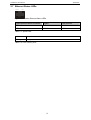
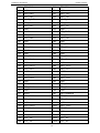
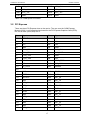
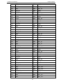
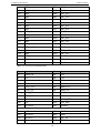
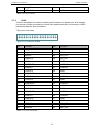
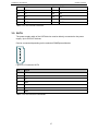
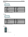
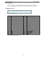
1
User’s Manual
CX-MB-ATX
COM Express Carrier Type 2
- PRELIMINARY Rev. 0.4
March 20th, 2008
CX-MB-ATX User's Manual
General Information
Preface
Copyright Notice
Copyright © 2008 MSC Vertriebs GmbH. All rights reserved.
Copying of this document, and giving it to others and the use or communication of the
contents thereof, are forbidden without express authority. Offenders are liable to the payment
of damages.
All rights are reserved in the event of the grant of a patent or the registration of a utility model
or design.
Important Information
This documentation is intended for qualified audience only. The product described herein is
not an end user product. It was developed and manufactured for further processing by
trained personnel.
Disclaimer
Although this document has been generated with the utmost care no warranty or liability for
correctness or suitability for any particular purpose is implied. The information in this
document is provided “as is”and is subject to change without notice.
EMC Rules
This unit has to be installed in a shielded housing. If not installed in a properly shielded
enclosure, and used in accordance with the instruction manual, this product may cause radio
interference in which case the user may be required to take adequate measures at his or her
own expense.
Trademarks
All used product names, logos or trademarks are property of their respective owners.
Certification
MSC Vertriebs GmbH is certified according to DIN EN ISO 9001:2000 standards.
Life-Cycle-Management
MSC products are developed and manufactured according to high quality standards. Our lifecycle-management assures long term availability through permanent product maintenance.
Technically necessary changes and improvements are introduced if applicable. A productchange-notification and end-of-life management process assures early information of our
customers.
Product Support
MSC engineers and technicians are committed to provide support to our customers
whenever needed.
Before contacting Technical Support of MSC Vertriebs GmbH, please consult the respective
pages on our web site at www.msc-ge.com/support-boards for the latest documentation,
drivers and software downloads.
If the information provided there does not solve your problem, please contact our Technical
Support:
Email: [email protected]
Phone: +49 8165 906-200
2
CX-MB-ATX User's Manual
General Information
Content
Content ................................................................................................................................ 3
List of figures........................................................................................................................ 5
List of tables ......................................................................................................................... 6
1 General Information........................................................................................................ 7
1.1 Revision History........................................................................................................ 7
2 Specification ................................................................................................................... 8
2.1 VGA.......................................................................................................................... 9
2.2 LAN .......................................................................................................................... 9
2.3 USB .......................................................................................................................... 9
2.4 Audio ........................................................................................................................ 9
2.5 Port 80...................................................................................................................... 9
2.6 Status LEDs.............................................................................................................. 9
2.6.1
5V_SBY ........................................................................................................... 9
2.6.2
12V .................................................................................................................. 9
2.6.3
HDD ................................................................................................................. 9
2.6.4
Type................................................................................................................. 9
2.6.5
Thrm ................................................................................................................ 9
2.7 Ethernet Status LEDs ............................................................................................. 10
3 Interface Connectors .................................................................................................... 11
3.1 COMExpress Connector ......................................................................................... 11
3.1.1
Rows A and B ................................................................................................ 11
3.1.2
Rows C and D................................................................................................ 14
3.2 PCI Express............................................................................................................ 17
3.3 PCI ......................................................................................................................... 20
3.4 LAN ........................................................................................................................ 22
3.5 USB ........................................................................................................................ 22
3.6 VGA........................................................................................................................ 23
3.7 LVDS ...................................................................................................................... 23
3.7.1
JILI ................................................................................................................. 24
3.7.2
JILI40 ............................................................................................................. 25
3.7.3
Backlight ........................................................................................................ 26
3.8 IDE ......................................................................................................................... 26
3.9 SATA ...................................................................................................................... 27
3.10 GPO ....................................................................................................................... 28
3.11 Misc ........................................................................................................................ 28
3.12 Audio ...................................................................................................................... 28
3.13 Super-IO ................................................................................................................. 29
3.14 Super-IO LPC ......................................................................................................... 29
3.14.1 Super-IO IO.................................................................................................... 30
3.14.2 COM1 ............................................................................................................ 30
3.14.3 COM2 ............................................................................................................ 31
3.14.4 PS/2 ............................................................................................................... 31
3.15 Jumper.................................................................................................................... 32
3.15.1 X501 .............................................................................................................. 32
3.15.2 J401 ............................................................................................................... 32
3.15.3 J402 ............................................................................................................... 33
3.15.4 J403 ............................................................................................................... 33
3.15.5 J404 ............................................................................................................... 33
3.15.6 J405 ............................................................................................................... 34
3.15.7 J406 ............................................................................................................... 34
3.15.8 J407 ............................................................................................................... 34
3.15.9 J408 ............................................................................................................... 34
3.15.10 J409 ............................................................................................................... 35
3.15.11 J410 ............................................................................................................... 35
4 Board Parameters ........................................................................................................ 36
4.1 COM Express ......................................................................................................... 36
3
CX-MB-ATX User's Manual
General Information
4.2 Network .................................................................................................................. 36
4.3 USB ........................................................................................................................ 36
4.4 Environmental Conditions ....................................................................................... 36
4.5 Battery .................................................................................................................... 36
5 NOTES......................................................................................................................... 37
4
CX-MB-ATX User's Manual
General Information
List of figures
Figure 2.1: Location of Connectors...............................................................................................................................8
Figure 2.2: Location of Rear Connectors ..................................................................................................................8
Figure 2.3: Location Ethernet Status LEDs ...........................................................................................................10
Figure 3.1: LAN Connector..............................................................................................................................................22
Figure 3.2: USB Connector..............................................................................................................................................22
Figure 3.3: VGA Connector .............................................................................................................................................23
Figure 3.4: Connector JILI................................................................................................................................................24
Figure 3.5: Connector JILI40 ..........................................................................................................................................25
Figure 3.6: Connector Backlight ...................................................................................................................................26
Figure 3.7: Connector DIE................................................................................................................................................26
Figure 3.8: Connector SATA...........................................................................................................................................27
Figure 3.9: Connector GPO.............................................................................................................................................28
Figure 3.10: Connector Misc...........................................................................................................................................28
Figure 3.11: Connector Audio ........................................................................................................................................28
Figure 3.12: Super-IO LPC..............................................................................................................................................29
Figure 3.13: Super-IO IO...................................................................................................................................................30
Figure 3.14: Connector COM1.......................................................................................................................................30
Figure 3.15: Connector COM2.......................................................................................................................................31
Figure 3.16: Connector PS/2 ..........................................................................................................................................31
Figure 3.17: X501 ..................................................................................................................................................................32
Figure 3.18: J401...................................................................................................................................................................32
Figure 3.19: J402...................................................................................................................................................................33
Figure 3.20: J403...................................................................................................................................................................33
Figure 3.21: J404...................................................................................................................................................................33
Figure 3.22: J405...................................................................................................................................................................34
Figure 3.23: J406...................................................................................................................................................................34
Figure 3.24: J407...................................................................................................................................................................34
Figure 3.25: J408...................................................................................................................................................................34
Figure 3.26: J409...................................................................................................................................................................35
Figure 3.27: J410...................................................................................................................................................................35
5
CX-MB-ATX User's Manual
General Information
List of tables
Table 2.1: Speed LED.............................................................................................................................................................10
Table 2.2: Link / Activity LED..............................................................................................................................................10
Table 3.1: COMExpress Connector................................................................................................................................14
Table 3.2: COMExpress Connector................................................................................................................................17
Table 3.3: Pin out PCI Express X201............................................................................................................................19
Table 3.4: Pin out PCI Express X202, 203.................................................................................................................20
Table 3.5: Pin out PCI.............................................................................................................................................................21
Table 3.6: Pin out LAN............................................................................................................................................................22
Table 3.7: Pin out USB Connector..................................................................................................................................22
Table 3.8: Pin out VGA Connector..................................................................................................................................23
Table 3.9: Signal description JILI interfaces .............................................................................................................24
Table 3.10: Pin out JILI ..........................................................................................................................................................25
Table 3.11: Pin out JILI40.....................................................................................................................................................25
Table 3.12: Pin out Backlight..............................................................................................................................................26
Table 3.13: Pin out IDE Connector.................................................................................................................................27
Table 3.14: Pin out SATA Connector ............................................................................................................................27
Table 3.15: Pin out GPO Connector ..............................................................................................................................28
Table 3.16: Pin out Misc Connector ...............................................................................................................................28
Table 3.17: Pin out Super-IO LPC...................................................................................................................................29
Table 3.18: Pin out Super-IO IO .......................................................................................................................................30
Table 3.19: Pin out COM1 Connector...........................................................................................................................30
Table 3.20: Pin out COM2 Connector...........................................................................................................................31
Table 3.21: Pin out PS/2 Connector...............................................................................................................................31
Table 3.22: Pin out X501.......................................................................................................................................................32
Table 3.23: Pin out J401........................................................................................................................................................32
Table 3.24: Pin out J402........................................................................................................................................................33
Table 3.25: Pin out J403........................................................................................................................................................33
Table 3.26: Pin out J404........................................................................................................................................................33
Table 3.27: Pin out J405........................................................................................................................................................34
Table 3.28: Pin out J406........................................................................................................................................................34
Table 3.29: Pin out J407........................................................................................................................................................34
Table 3.30: Pin out J408........................................................................................................................................................34
Table 3.31: Pin out J409........................................................................................................................................................35
Table 3.32: Pin out J410........................................................................................................................................................35
6
CX-MB-ATX User's Manual
General Information
1 General Information
1.1 Revision History
Rev.
Date
0.1
Description
Initial version
0.2
13.07.2007
New layout
0.3
23.07.2007
New layout
0.4
20.03.2008
Preface added
7
CX-MB-ATX User's Manual
Specification
2 Specification
The CX-MB-ATX is a COMExpress Carrier board for Basic and Extended Form factor.
It supports COMExpress module with type 2 and needs an ATX12V power supply.
1
IDE
Speaker
COM2
1
ATX
SIO
IO
1
1
Extended Formfactor
Batterie
1
J405
Backlight
PS/2
1
J406
COM1
SIO
LPC
ATX12V
1
1
1
1
Basic Formfactor
J402
1
GPO
SATA1 SATA3
J403
MACH 5512
1
BIOS
X501
SATA2 SATA0
JILI
1
MISC
1
CON A-B
JILI40
CON C-D
1
5VS
HD
12V
THRM
TYPE
J408
J409
1
J404 J401
J407
USB
1+2
VGA
USB
1+2
USB
3+4
GbE
Audio
Figure 2.1: Location of Connectors
Figure 2.2: Location of Rear Connectors
8
J410
PEG
PCI
PCIe x1
PCIe x1
PCI
Power
Reset
CX-MB-ATX User's Manual
Specification
2.1 VGA
If a CRT monitor is used, a standard VGA cable (15 pins) is connected between the
monitor and the VGA connector of the carrier board. Make sure that your monitor is
capable of displaying the video resolutions. If a video mode generates horizontal
frequencies much higher than the maximum value of your monitor, the monitor may be
damaged! If your monitor is not able to display a mode, switch off or disconnect the
monitor in advance and select an appropriate video mode for the monitor.
2.2 LAN
A Network can be connected using 10BaseT, 100BaseTX or 1000BaseT standard
(depends on the module).
2.3 USB
Up to four USB devices can be connected to the carrier board. A standard USB mouse
and a standard USB keyboard can be connected to a USB connector.
2.4 Audio
There are connectors for Line In, Line Out and Microphone.
2.5 Port 80
This Display shows the Port80 debug information (Postcode) of the BIOS.
2.6 Status LEDs
2.6.1
5V_SBY
This green LED shows the presence of the 5V standby voltage from the ATX main
power.
2.6.2
12V
This green LED shows the presence of the 12V voltage from the ATX main power.
2.6.3
HDD
This yellow LED shows activity on either the IDE interface or the SATA interfaces.
2.6.4
Type
This red LED shows a mismatch of the COMExpress types. The CX-MB-ATX carrier
board is designed for type 2 COMExpress modules and can not used with other types.
The main power will not turn on if there is a mismatch.
2.6.5
Thrm
This red LED shows a critical thermal shutdown of the system.
9
CX-MB-ATX User's Manual
Specification
2.7 Ethernet Status LEDs
Link/Activity
Speed
Figure 2.3: Location Ethernet Status LEDs
COM Express Ethernet Controller
Gigabit
Fast Ethernet
LED on
1000 Mb/s
100 Mb/s
LED off
100 Mb/s or less
10Mb/s or less
Table 2.1: Speed LED
yellow
link pulse detected
blinking
Activity
Table 2.2: Link / Activity LED
10
CX-MB-ATX User's Manual
3
Interface Connectors
Interface Connectors
3.1 COMExpress Connector
3.1.1
Rows A and B
Row A
Row B
A1
GND
B1
GND
A2
GBE0_MDI3-
B2
GBE0_ACT#
A3
GBE0_MDI3+
B3
LPC_FRAME#
A4
GBE0_LINK100#
B4
LPC_AD0
A5
GBE0_LINK1000#
B5
LPC_AD1
A6
GBE0_MDI2-
B6
LPC_AD2
A7
GBE0_MDI2+
B7
LPC_AD3
A8
GBE0_LINK#
B8
LPC_DRQ0#
A9
GBE0_MDI1-
B9
LPC_DRQ1#
A10
GBE0_MDI1+
B10
LPC_CLK
A11
GND
B11
GND
A12
GBE0_MDI0-
B12
PWRBTN#
A13
GBE0_MDI0+
B13
SMB_CK
A14
GBE0_CTREF
B14
SMB_DAT
A15
SUS_S3#
B15
SMB_ALERT#
A16
SATA0_TX+
B16
SATA1_TX+
A17
SATA0_TX-
B17
SATA1_TX-
A18
SUS_S4#
B18
SUS_STAT#
A19
SATA0_RX+
B19
SATA1_RX+
A20
SATA0_RX-
B20
SATA1_RX-
A21
GND
B21
GND
A22
SATA2_TX+
B22
SATA3_TX+
A23
SATA2_TX-
B23
SATA3_TX-
A24
SUS_S5#
B24
PWR_OK
A25
SATA2_RX+
B25
SATA3_RX+
A26
SATA2_RX-
B26
SATA3_RX-
A27
BATLOW#
B27
WDT
A28
ATA_ACT#
B28
AC_SDIN2
A29
AC_SYNC
B29
AC_SDIN1
A30
AC_RST#
B30
AC_SDIN0
A31
GND
B31
GND
A31
GND
B31
GND
11
CX-MB-ATX User's Manual
Interface Connectors
A32
AC_BITCLK
B32
SPKR
A33
AC_SDOUT
B33
I2C_CK
A34
BIOS_DISABLE#
B34
I2C_DAT
A35
THRMTRIP#
B35
THRM#
A36
USB6-
B36
USB7-
A37
USB6+
B37
USB7+
A38
USB_6_7_OC#
B38
USB_4_5_OC#
A39
USB4-
B39
USB5-
A40
USB4+
B40
USB5+
A41
GND
B41
GND
A42
USB2-
B42
USB3-
A43
USB2+
B43
USB3+
A44
USB_2_3_OC#
B44
USB_0_1_OC#
A45
USB0-
B45
USB1-
A46
USB0+
B46
USB1+
A47
VCC_RTC
B47
EXCD1_PERST#
A48
EXCD0_PERST#
B48
EXCD1_CPPE#
A49
EXCD0_CPPE#
B49
SYS_RESET#
A50
LPC_SERIRQ
B50
CB_RESET#
A51
GND
B51
GND
A52
PCIE_TX5+
B52
PCIE_RX5+
A53
PCIE_TX5-
B53
PCIE_RX5-
A54
GPI0
B54
GPO1
A55
PCIE_TX4+
B55
PCIE_RX4+
A56
PCIE_TX4-
B56
PCIE_RX4-
A57
GND
B57
GPO2
A58
PCIE_TX3+
B58
PCIE_RX3+
A59
PCIE_TX3-
B59
PCIE_RX3-
A60
GND
B60
GND
A61
PCIE_TX2+
B61
PCIE_RX2+
A62
PCIE_TX2-
B62
PCIE_RX2-
A63
GPI1
B63
GPO3
A64
PCIE_TX1+
B64
PCIE_RX1+
A65
PCIE_TX1-
B65
PCIE_RX1-
A66
GND
B66
WAKE0#
A67
GPI2
B67
WAKE1#
A68
PCIE_TX0+
B68
PCIE_RX0+
A69
PCIE_TX0-
B69
PCIE_RX0-
12
CX-MB-ATX User's Manual
Interface Connectors
A70
GND
B70
GND
A71
LVDS_A0+
B71
LVDS_B0+
A72
LVDS_A0-
B72
LVDS_B0-
A73
LVDS_A1+
B73
LVDS_B1+
A74
LVDS_A1-
B74
LVDS_B1-
A75
LVDS_A2+
B75
LVDS_B2+
A76
LVDS_A2-
B76
LVDS_B2-
A77
LVDS_VDD_EN
B77
LVDS_B3+
A78
LVDS_A3+
B78
LVDS_B3-
A79
LVDS_A3-
B79
LVDS_BKLT_EN
A80
GND
B80
GND
A81
LVDS_A_CK+
B81
LVDS_B_CK+
A82
LVDS_A_CK-
B82
LVDS_B_CK-
A83
LVDS_I2C_CK
B83
LVDS_BKLT_CTRL
A84
LVDS_I2C_DAT
B84
VCC_5V_SBY
A85
GPI3
B85
VCC_5V_SBY
A86
KBD_RST#
B86
VCC_5V_SBY
A87
KBD_A20GATE
B87
VCC_5V_SBY
A88
PCIE0_CK_REF+
B88
RSVD
A89
PCIE0_CK_REF-
B89
VGA_RED
A90
GND
B90
GND
A91
RSVD
B91
VGA_GRN
A92
RSVD
B92
VGA_BLU
A93
GPO0
B93
VGA_HSYNC
A94
RSVD
B94
VGA_VSYNC
A95
RSVD
B95
VGA_I2C_CK
A96
GND
B96
VGA_I2C_DAT
A97
VCC_12V
B97
TV_DAC_A
A98
VCC_12V
B98
TV_DAC_B
A99
VCC_12V
B99
TV_DAC_C
A100
GND
B100
GND
A101
VCC_12V
B101
VCC_12V
A102
VCC_12V
B102
VCC_12V
A103
VCC_12V
B103
VCC_12V
A104
VCC_12V
B104
VCC_12V
A105
VCC_12V
B105
VCC_12V
A106
VCC_12V
B106
VCC_12V
A107
VCC_12V
B107
VCC_12V
13
CX-MB-ATX User's Manual
Interface Connectors
A108
VCC_12V
B108
VCC_12V
A109
VCC_12V
B109
VCC_12V
A110
GND
B110
GND
Table 3.1: COMExpress Connector
3.1.2
Rows C and D
Row C
Row D
C1
GND
D1
GND
C2
IDE_D7
D2
IDE_D5
C3
IDE_D6
D3
IDE_D10
C4
IDE_D3
D4
IDE_D11
C5
IDE_D15
D5
IDE_D12
C6
IDE_D8
D6
IDE_D4
C7
IDE_D9
D7
IDE_D0
C8
IDE_D2
D8
IDE_REQ
C9
IDE_D13
D9
IDE_IOW#
C10
IDE_D1
D10
IDE_ACK#
C11
GND
D11
GND
C12
IDE_D14
D12
IDE_IRQ
C13
IDE_IORDY
D13
IDE_A0
C14
IDE_IOR#
D14
IDE_A1
C15
PCI_PME#
D15
IDE_A2
C16
PCI_GNT2#
D16
IDE_CS1#
C17
PCI_REQ2#
D17
IDE_CS3#
C18
PCI_GNT1#
D18
IDE_RESET#
C19
PCI_REQ1#
D19
PCI_GNT3#
C20
PCI_GNT0#
D20
PCI_REQ3#
C21
GND
D21
GND
C22
PCI_REQ0#
D22
PCI_AD1
C23
PCI_RESET#
D23
PCI_AD3
C24
PCI_AD0
D24
PCI_AD5
C25
PCI_AD2
D25
PCI_AD7
C26
PCI_AD4
D26
PCI_C/BE0#
C27
PCI_AD6
D27
PCI_AD9
C28
PCI_AD8
D28
PCI_AD11
C29
PCI_AD10
D29
PCI_AD13
C30
PCI_AD12
D30
PCI_AD15
C31
GND
D31
GND
14
CX-MB-ATX User's Manual
Interface Connectors
C31
GND
D31
GND
C32
PCI_AD14
D32
PCI_PAR
C33
PCI_C/BE1#
D33
PCI_SERR#
C34
PCI_PERR#
D34
PCI_STOP#
C35
PCI_LOCK#
D35
PCI_TRDY#
C36
PCI_DEVSEL#
D36
PCI_FRAME#
C37
PCI_IRDY#
D37
PCI_AD16
C38
PCI_C/BE2#
D38
PCI_AD18
C39
PCI_AD17
D39
PCI_AD20
C40
PCI_AD19
D40
PCI_AD22
C41
GND
D41
GND
C42
PCI_AD21
D42
PCI_AD24
C43
PCI_AD23
D43
PCI_AD26
C44
PCI_C/BE3#
D44
PCI_AD28
C45
PCI_AD25
D45
PCI_AD30
C46
PCI_AD27
D46
PCI_IRQC#
C47
PCI_AD29
D47
PCI_IRQD#
C48
PCI_AD31
D48
PCI_CLKRUN#
C49
PCI_IRQA#
D49
PCI_M66EN
C50
PCI_IRQB#
D50
PCI_CLK
C51
GND
D51
GND
C52
PEG_RX0+
D52
PEG_TX0+
C53
PEG_RX0-
D53
PEG_TX0-
C54
TYPE0#
D54
PEG_LANE_RV#
C55
PEG_RX1+
D55
PEG_TX1+
C56
PEG_RX1-
D56
PEG_TX1-
C57
TYPE1#
D57
TYPE2#
C58
PEG_RX2+
D58
PEG_TX2+
C59
PEG_RX2-
D59
PEG_TX2-
C60
GND
D60
GND
C61
PEG_RX3+
D61
PEG_TX3+
C62
PEG_RX3-
D62
PEG_TX3-
C63
RSVD
D63
RSVD
C64
RSVD
D64
RSVD
C65
PEG_RX4+
D65
PEG_TX4+
C66
PEG_RX4-
D66
PEG_TX4-
C67
RSVD
D67
GND
C68
PEG_RX5+
D68
PEG_TX5+
15
CX-MB-ATX User's Manual
Interface Connectors
C69
PEG_RX5-
D69
PEG_TX5-
C70
GND
D70
GND
C71
PEG_RX6+
D71
PEG_TX6+
C72
PEG_RX6-
D72
PEG_TX6-
C73
SDVO_DATA
D73
SDVO_CLK
C74
PEG_RX7+
D74
PEG_TX7+
C75
PEG_RX7-
D75
PEG_TX7-
C76
GND
D76
GND
C77
RSVD
D77
IDE_CBLID#
C78
PEG_RX8+
D78
PEG_TX8+
C79
PEG_RX8-
D79
PEG_TX8-
C80
GND
D80
GND
C81
PEG_RX9+
D81
PEG_TX9+
C82
PEG_RX9-
D82
PEG_TX9-
C83
RSVD
D83
RSVD
C84
GND
D84
GND
C85
PEG_RX10+
D85
PEG_TX10+
C86
PEG_RX10-
D86
PEG_TX10-
C87
GND
D87
GND
C88
PEG_RX11+
D88
PEG_TX11+
C89
PEG_RX11-
D89
PEG_TX11-
C90
GND
D90
GND
C91
PEG_RX12+
D91
PEG_TX12+
C92
PEG_RX12-
D92
PEG_TX12-
C93
GND
D93
GND
C94
PEG_RX13+
D94
PEG_TX13+
C95
PEG_RX13-
D95
PEG_TX13-
C96
GND
D96
GND
C97
RSVD
D97
PEG_ENABLE#
C98
PEG_RX14+
D98
PEG_TX14+
C99
PEG_RX14-
D99
PEG_TX14-
C100
GND
D100
GND
C101
PEG_RX15+
D101
PEG_TX15+
C102
PEG_RX15-
D102
PEG_TX15-
C103
GND
D103
GND
C104
VCC_12V
D104
VCC_12V
C105
VCC_12V
D105
VCC_12V
C106
VCC_12V
D106
VCC_12V
16
CX-MB-ATX User's Manual
Interface Connectors
C107
VCC_12V
D107
VCC_12V
C108
VCC_12V
D108
VCC_12V
C109
VCC_12V
D109
VCC_12V
C110
GND
D110
GND
Table 3.2: COMExpress Connector
3.2 PCI Express
There are three PCI Express slots on the carrier. The one near the COM Express
Module (X201) is x16 organized and used for the PCI Express Graphics Card (PEG),
the rest of them (X202,203) are x1.
Pin
Signal
Pin
Signal
A1
PRSNT1#
B1
12V
A2
12V
B2
12V
A3
12V
B3
12V
A4
GND
B4
GND
A5
JTAG_TCK
B5
SMB_CLK
A6
JTAG_TDI
B6
SMB_DAT
A7
JTAG_TDO
B7
GND
A8
JTAG_TMS
B8
3V3
A9
3V3
B9
JTAG_RST#
A10
3V3
B10
3V3_AUX
A11
PE_RST#
B11
WAKE#
A12
GND
B12
RSVD
A13
REFCLK+
B13
GND
A14
REFCLK-
B14
PET_p0
A15
GND
B15
PET_n0
A16
PER_p0
B16
GND
A17
PER_n0
B17
PRSNT2#
A18
GND
B18
GND
A19
RSVD
B19
PET_p1
A20
GND
B20
PET_n1
A21
PER_p1
B21
GND
A22
PER_n1
B22
GND
A23
GND
B23
PET_p2
A24
GND
B24
PET_n2
A25
PER_p2
B25
GND
KEY
17
CX-MB-ATX User's Manual
Interface Connectors
A26
PER_n2
B26
GND
A27
GND
B27
PET_p3
A28
GND
B28
PET_n3
A29
PER_p3
B29
GND
A30
PER_n3
B30
RSVD
A31
GND
B31
PRSNT2#
A32
RSVD
B32
GND
A33
RSVD
B33
PET_p4 1
A34
GND
B34
PET_n4 1
A35
PER_p4 1
B35
GND
A36
PER_n4
1
B36
GND
A37
GND
B37
PET_p5 1
A38
GND
B38
PET_n5 1
A39
PER_p5 1
B39
GND
A40
PER_n5 1
B40
GND
A41
GND
B41
PET_p6 1
A42
GND
B42
PET_n6 1
A43
PER_p6 1
B43
GND
A44
PER_n6
1
B44
GND
A45
GND
B45
PET_p7 1
A46
GND
B46
PET_n7 1
A47
PER_p7 1
B47
GND
A48
PER_n7 1
B48
PRSNT2#
A49
GND
B49
GND
A50
RSVD
B50
PET_p8 1
A51
GND
B51
PET_n8 1
A52
PER_p8 1
B52
GND
A53
PER_n8 1
B53
GND
A54
GND
B54
PET_p9 1
A55
GND
B55
PET_n9 1
A56
PER_p9 1
B56
GND
A57
PER_n9
1
B57
GND
A58
GND
B58
PET_p10 1
A59
GND
B59
PET_n10 1
A60
PER_p10 1
B60
GND
A61
PER_n10 1
B61
GND
A62
GND
B62
PET_p11 1
A63
GND
B63
PET_n11 1
18
CX-MB-ATX User's Manual
Interface Connectors
A64
PER_p11 1
B64
GND
A65
PER_n11 1
B65
GND
A66
GND
B66
PET_p12 1
A67
GND
B67
PET_n12 1
A68
PER_p12 1
B68
GND
A69
PER_n12
1
B69
GND
A70
GND
B70
PET_p13 1
A71
GND
B71
PET_n13 1
A72
PER_p13 1
B72
GND
A73
PER_n13 1
B73
GND
A74
GND
B74
PET_p14 1
A75
GND
B75
PET_n14 1
A76
PER_p14 1
B76
GND
A77
PER_n14 1
B77
GND
A78
GND
B78
PET_p15 1
A79
GND
B79
PET_n15 1
A80
PER_p15 1
B80
GND
A81
PER_n15
1
B81
PRSNT2#
A82
GND
B82
RSVD
Table 3.3: Pin out PCI Express X201
Pin
Signal
Pin
Signal
A1
PRSNT1#
B1
12V
A2
12V
B2
12V
A3
12V
B3
12V
A4
GND
B4
GND
A5
JTAG_TCK
B5
SMB_CLK
A6
JTAG_TDI
B6
SMB_DAT
A7
JTAG_TDO
B7
GND
A8
JTAG_TMS
B8
3V3
A9
3V3
B9
JTAG_RST#
A10
3V3
B10
3V3_AUX
A11
PE_RST#
B11
WAKE#
A12
GND
B12
RSVD
A13
REFCLK+
B13
GND
A14
REFCLK-
B14
PET_p0
A15
GND
B15
PET_n0
KEY
19
CX-MB-ATX User's Manual
Interface Connectors
A16
PER_p0
B16
GND
A17
PER_n0
B17
PRSNT2#
A18
GND
B18
GND
Table 3.4: Pin out PCI Express X202, 203
3.3 PCI
Pin
Signal
Pin
Signal
A1
TRST#
B1
-12V
A2
12V
B2
TCK
A3
TMS
B3
GND
A4
TDI
B4
TDO
A5
5V
B5
5V
A6
INTA#
B6
5V
A7
INTC#
B7
INTB#
A8
5V
B8
INTD#
A9
RSVD
B9
PRSNT1#
A10
5V
B10
RSVD
A11
RSVD
B11
PRSNT2#
A12
GND
B12
GND
A13
GND
B13
GND
A14
3V3
B14
RSVD
A15
RST#
B15
GND
A16
5V
B16
CLK
A17
GNT#
B17
GND
A18
GND
B18
REQ#
A19
PME#
B19
5V
A20
AD30
B20
AD31
A21
3V3
B21
AD29
A22
AD28
B22
GND
A23
AD26
B23
AD27
A24
GND
B24
AD25
A25
AD24
B25
3V3
A26
IDSEL
B26
C/BE3#
A27
3V3
B27
AD23
A28
AD22
B28
GND
A29
AD20
B29
AD21
A30
GND
B30
AD19
20
CX-MB-ATX User's Manual
Interface Connectors
A31
AD18
B31
3V3
A32
AD16
B32
AD17
A33
3V3
B33
C/BE2#
A34
FRAME#
B34
GND
A35
GND
B35
IRDY#
A36
TRDY#
B36
3V3
A37
GND
B37
DEVSEL#
A38
STOP#
B38
GND
A39
3V3
B39
LOCK#
A40
SMBCLK
B40
PERR#
A41
SMBDAT
B41
3V3
A42
GND
B42
SERR#
A43
PAR
B43
3V3
A44
AD15
B44
C/BE1#
A45
3V3
B45
AD14
A46
AD13
B46
GND
A47
AD11
B47
AD12
A48
GND
B48
AD10
A49
AD09
B49
GND
A52
C/BE0#
B52
AD08
A53
3V3
B53
AD07
A54
AD06
B54
3V3
A55
AD04
B55
AD05
A56
GND
B56
AD03
A57
AD02
B57
GND
A58
AD00
B58
AD01
A59
5V
B59
5V
A60
REQ64#
B60
ACK64#
A61
5V
B61
5V
A62
5V
B62
5V
Key
Table 3.5: Pin out PCI
21
CX-MB-ATX User's Manual
Interface Connectors
3.4 LAN
8 76 54 3 21
Figure 3.1: LAN Connector
Pin
Signal
1
LAN1 Pair0+
2
LAN1 Pair0-
3
LAN1 Pair1+
4
LAN1 Pair2+
5
LAN1 Pair2-
6
LAN1 Pair1-
7
LAN1 Pair3+
8
LAN1 Pair3-
Table 3.6: Pin out LAN
3.5 USB
1
2
3 4
1
2
3 4
Figure 3.2: USB Connector
Pin
Signal
1
5V
2
USB +
3
USB -
4
GND
Table 3.7: Pin out USB Connector
22
CX-MB-ATX User's Manual
Interface Connectors
3.6 VGA
5
1
6
10
15
11
Figure 3.3: VGA Connector
10-Pin
15-Pin
Connector
VGA-Connector
Pin
Signal
Pin
1
CRTRED
1
2
GND
5
3
CRTGREEN
2
4
GND
6
5
CRTBLUE
3
6
GND
7, 8, 10
7
VGA_DDCDATA
12
8
VGA_HSYNC
13
9
VGA_VSYNC
14
10
VGA_DOCCLK
15
Table 3.8: Pin out VGA Connector
3.7 LVDS
The LVDS interface is implemented as two different JILI interfaces.
Signal Name
LCDDO0
LCDDO1
LCDDO2
LCDDO3
LCDDO4
LCDDO5
LCDDO6
LCDDO7
LCDDO8
LCDDO9
LCDDO10
LCDDO11
LCDDO12
LCDDO13
LCDDO14
LCDDO15
LCDDO16
1 Pixel / Clock LVDS mode
LVD0LVD0+
LVD1LVD1+
LVD2LVD2+
LVDCLVDC+
LVD3- (opt.24Bit)
LVD3+ (opt.24Bit)
23
2 Pixel / Clock LVDS mode
odd LVD0odd LVD0+
odd LVD1odd LVD1+
odd LVD2odd LVD2+
odd LVDCodd LVDC+
odd LVD3- (opt.24Bit)
odd LVD3+ (opt.24Bit)
even LVD0even LVD0+
even LVD1even LVD1+
even LVD2even LVD2+
even LVDC-
CX-MB-ATX User's Manual
LCDDO17
LCDDO18
LCDDO19
JILI_DAT
JILI_CLK
ENAVDD
-ENABKL
GND
BKLGND
+5V
+12V
SW_VDD
SW_BACK
BRIGHT
Interface Connectors
even LVDC+
even LVD3- (opt.24Bit)
even LVD3+ (opt.24Bit)
JILI EEPROM I2C Data
JILI EEPROM I2C Clock
panel power enable
backlight power enable, active low!!!
power return
(backlight power return)
fixed 5V
fixed 12V
switched panel power (enabled by ENAVDD)
switched backlight power (enabled by ENABKL)
backlight brightness control signal
Table 3.9: Signal description JILI interfaces
3.7.1
JILI
JILI is intended to be used as standard interface with a 40 pin, 0,5mm Flat Foil
Connection (FFC). All signals are "final" and do not need any further processing.
40
1
Figure 3.4: Connector JILI
Pin
Function
Pin
Function
1
-
21
LCDDO13
2
LCDDO0
22
-
3
LCDDO1
23
LCDDO14
4
ENAVDD
24
LCDDO15
5
LCDDO2
25
GND
6
LCDDO3
26
LCDDO16
7
-
27
LCDDO17
8
LCDDO4
28
GND
9
LCDDO5
29
LCDDO18
10
GND
30
LCDDO19
11
LCDDO6
31
+5V
12
LCDDO7
32
+5V
13
GND
33
+5V
14
LCDDO8
34
+5V
15
LCDDO9
35
ENABKL
16
JILI_DAT
36
BKLGND
17
LCDDO10
37
BKLGND
18
LCDDO11
38
+12V
24
CX-MB-ATX User's Manual
Interface Connectors
19
JILI_CLK
39
+12V
20
LCDDO12
40
+12V
Table 3.10: Pin out JILI
3.7.2
JILI40
JILI40 is intended to be used as a direct panel interface. All signals are "final" and do
not need any further processing. It should be implemented when connecting to LVDS
panels with discrete wire connectors.
This port is not tested.
2
40
1
39
Figure 3.5: Connector JILI40
Pin
Function
Pin
Function
1
SW_BACK/ENABKL
21
GND
2
SW_BACK/ENABKL
22
GND
3
BRIGHT
23
JILI_CLK
4
LCDDO19
24
JILI_DAT
5
LCDDO18
25
GND
6
RESERVED
26
LCDDO7
7
LCDDO17
27
LCDDO6
8
LCDDO16
28
GND
9
RESERVED
29
LCDDO5
10
LCDDO15
30
LCDDO4
11
LCDDO14
31
GND
12
RESERVED
32
LCDDO3
13
LCDDO13
33
LCDDO2
14
LCDDO12
34
GND
15
RESERVED
35
LCDDO1
16
LCDDO11
36
LCDDO0
17
LCDDO10
37
GND
18
RESERVED
38
GND
19
LCDDO9
39
SW_VDD
20
LCDDO8
40
SW_VDD
Table 3.11: Pin out JILI40
25
CX-MB-ATX User's Manual
3.7.3
Interface Connectors
Backlight
This port is not tested.
5
1
Figure 3.6: Connector Backlight
Pin
1
2
3
4
5
Signal
VCC
GND
BLON#
VCON
GND
Function
Supply Voltage
Ground
Backlight On
Brightness Control
Ground
Table 3.12: Pin out Backlight
3.8 IDE
The power supply cable of the EIDE device must be directly connected to the power
supply. Up to two EIDE drives
(Hard disk, CD-ROM) can be connected. Cable length should not exceed 40 cm to
avoid instable operation. It is also recommended to use an UDMA-Cable with 80 wires.
2
40
1
39
Figure 3.7: Connector DIE
Pin
Signal
Pin
Signal
1
/RST
2
GND
3
D7
4
D8
5
D6
6
D9
7
D5
8
D10
9
D4
10
D11
11
D3
12
D12
13
D2
14
D13
15
D1
16
D14
17
D0
18
D15
19
GND
20
nc
21
REQ
22
GND
23
/IOW
24
GND
25
/IOR
26
GND
27
IORDY
28
nc
26
CX-MB-ATX User's Manual
Interface Connectors
29
/ACK
30
GND
31
IRQ14
32
nc
33
A1
34
nc
35
A0
36
A2
37
/CS1
38
/CS3
39
/ACT
40
GND
Table 3.13: Pin out IDE Connector
3.9 SATA
The power supply cable of the SATA device must be directly connected to the power
supply. Up to four SATA drives
Can be connected depending on the selected COMExpress Module.
1
Figure 3.8: Connector SATA
Pin
Signal
1
GND
2
TX+
3
TX-
4
GND
5
RX-
6
RX+
7
GND
Table 3.14: Pin out SATA Connector
27
CX-MB-ATX User's Manual
Interface Connectors
3.10 GPO
2
10
1
9
Figure 3.9: Connector GPO
Pin
Signal
Pin
Signal
1
Reserved
2
GND
3
Reserved
4
GND
5
Reserved
6
GND
7
Reserved
8
GND
9
Reserved
10
GND
Table 3.15: Pin out GPO Connector
3.11 Misc
2
10
1
9
Figure 3.10: Connector Misc
Pin
Signal
Pin
Signal
1
/PWRBTN
2
+5V
3
GND
4
GND
5
/SYSRESET
6
GND
7
GND
8
SPEAKER
9
LED_ATA-
10
LED_ATA+
Table 3.16: Pin out Misc Connector
3.12 Audio
Line In
Line Out
Microfon
Figure 3.11: Connector Audio
28
CX-MB-ATX User's Manual
Interface Connectors
3.13 Super-IO
There is no Super-IO on the CX-MB-ATX. If you need the function of a Super-IO, you
have to put a piggy board on the Super-IO LPC and the Super-IO IO connectors.
3.14 Super-IO LPC
2
36
1
35
Figure 3.12: Super-IO LPC
Pin
1
3
5
7
9
11
13
15
17
19
21
23
25
27
29
31
33
35
Signal
+5V
nc
+3V3
+3V3_SBY
GND
GND
LPC_AD1
LPC_AD3
GND
GND
GND
GND
GND
GND
GND
GND
GND
GND
Pin
2
4
6
8
10
12
14
16
18
20
22
24
26
28
30
32
34
36
Table 3.17: Pin out Super-IO LPC
29
Signal
+5V
+3V3
nc
GND
nc
LPC_AD0
LPC_AD2
LPC_FRAME#
LPC_DRQ0#
LPC_CLK
SUS_STAT#
WAKE1#
nc
LPC_SERIRQ
PCI_CLKRUN#
LPC_DRQ1#
KBD_RST#
GND
CX-MB-ATX User's Manual
3.14.1
Interface Connectors
Super-IO IO
2
36
1
35
Figure 3.13: Super-IO IO
Pin
1
3
5
7
9
11
13
15
17
19
21
23
25
27
29
31
33
35
Signal
SMB_CLK
SMB_DAT
KBDAT
KBCLK
MSDAT
MSCLK
NC
NC
NC
NC
COM1_DCD#
COM1_RXD
COM1_TXD
COM1_DTR#
COM1_DSR#
COM1_RTS#
COM1_CTS#
COM1_RI#
Pin
2
4
6
8
10
12
14
16
18
20
22
24
26
28
30
32
34
36
Signal
SLP_S3#
SLP_S4#
SLP_S5#
EXT_THRM#
SMBALERT#
NC
THRMTRIP#
BATLOW#
NC
NC
COM2_DCD#
COM2_RXD
COM2_TXD
COM2_DTR#
COM2_DSR#
COM2_RTS#
COM2_CTS#
COM2_RI#
Table 3.18: Pin out Super-IO IO
3.14.2
COM1
The pins of the connector COM1 are the RS232 driven pins of the Super-IO IO
connector. Use this connector only, if you have a Super IO piggy board installed.
2
10
1
9
Figure 3.14: Connector COM1
Pin
Signal
Pin
Signal
1
COM1_DCD#
2
COM1_DSR#
3
COM1_RXD
4
COM1_RTS#
5
COM1_TXD
6
COM1_CTS#
7
COM1_DTR#
8
COM1_RI#
9
GND
10
nc
Table 3.19: Pin out COM1 Connector
30
CX-MB-ATX User's Manual
3.14.3
Interface Connectors
COM2
The pins of the connector COM2 are the RS232 driven pins of the Super-IO IO
connector. Use this connector only, if you have a Super IO piggy board installed.
2
10
1
9
Figure 3.15: Connector COM2
Pin
Signal
Pin
Signal
1
COM2_DCD#
2
COM2_DSR#
3
COM2_RXD
4
COM2_RTS#
5
COM2_TXD
6
COM2_CTS#
7
COM2_DTR#
8
COM2_RI#
9
GND
10
nc
Table 3.20: Pin out COM2 Connector
3.14.4
PS/2
The pins of the connector PS/2 are directly connected to the according pins on the
Super-IO IO connector. Use this connector only, if you have a Super IO piggy board
installed.
2
8
1
7
Figure 3.16: Connector PS/2
Pin
Signal
Pin
Signal
1
+5V
2
+5V
3
KB_DAT
4
MS_DAT
5
KB_CLK
6
MS_CLK
7
GND
8
GND
Table 3.21: Pin out PS/2 Connector
31
CX-MB-ATX User's Manual
Interface Connectors
3.15 Jumper
3.15.1
X501
2
20
1
19
Figure 3.17: X501
Pos
Signal
Function
1-2
/BIOSDISABLE
Set jumper to disable On-Module-BIOS and enable OnCarrier-BIOS.
3-4
RESERVED
Reserved function, do not set.
5-6
RESERVED
Reserved function, do not set.
7-8
RESERVED
Reserved function, do not set.
9-10
RESERVED
Reserved function, do not set.
11-12
RESERVED
Reserved function, do not set.
13-14
RESERVED
Reserved function, do not set.
15-16
RESERVED
Reserved function, do not set.
17-18
RESERVED
Reserved function, do not set.
19-20
RESERVED
Reserved function, do not set.
Table 3.22: Pin out X501
3.15.2
J401
Thos jumper selects the voltage for the LVDS panel.
1
3
Figure 3.18: J401
Pos
1-2
2-3
Function
Panel voltage is 5 V.
Panel voltage is 3,3 V.
Table 3.23: Pin out J401
32
CX-MB-ATX User's Manual
3.15.3
Interface Connectors
J402
Thos jumper selects the voltage for the backlight of the LVDS panel.
2
6
1
5
Figure 3.19: J402
Pos
1-2
3-4
5-6
Function
Backlight voltage is 3,3 V.
Backlight voltage is 5 V.
Backlight voltage is 12 V.
Table 3.24: Pin out J402
3.15.4
J403
This jumper controls the last 3 bit of the I2C address of the EDID EEPROM.
2
6
1
5
Figure 3.20: J403
Pos
1-2
3-4
5-6
Function
Insert to set the bit A0 of the I2C address to 1.
Insert to set the bit A1 of the I2C address to 1.
Insert to set the bit A2 of the I2C address to 1.
Table 3.25: Pin out J403
3.15.5
J404
This jumper selects the polarity of the signal LVDS_VDD_ENABLE which enables the
LVDS panel power.
1
3
Figure 3.21: J404
Pos
1-2
2-3
Function
LVDS_VDD_ENABLE is active low.
LVDS_VDD_ENABLE is active high.
Table 3.26: Pin out J404
33
CX-MB-ATX User's Manual
3.15.6
Interface Connectors
J405
This jumper selects the polarity of the signal LVDS_BKLT_ENABLE which enables the
LVDS backlight power.
1
3
Figure 3.22: J405
Pos
1-2
2-3
Function
LVDS_BKLT_ENABLE is active high.
LVDS_BKLT_ENABLE is active low.
Table 3.27: Pin out J405
3.15.7
J406
This jumper selects the maximum level of the signal BKLT_BRIGHT which controls the
brightness of the backlight.
1
3
Figure 3.23: J406
Pos
1-2
2-3
Function
Maximum level is 5 V.
Maximum level is 3,3 V.
Table 3.28: Pin out J406
3.15.8
J407
This jumper selects the mode of the Ethernet controller on the COM Express module.
1
2
Figure 3.24: J407
Pos
1-2
Function
Insert to use a Gigabit Ethernet Controller on the COM Express module.
Table 3.29: Pin out J407
3.15.9
J408
This jumper selects the mode of the Ethernet controller on the COM Express module.
1
2
Figure 3.25: J408
Pos
1-2
Function
Insert to use a Gigabit Ethernet Controller on the COM Express module.
Table 3.30: Pin out J408
34
CX-MB-ATX User's Manual
3.15.10
Interface Connectors
J409
This jumper selects the mode of the Ethernet controller on the COM Express module.
1
2
Figure 3.26: J409
Pos
1-2
Function
Insert to use a Gigabit Ethernet Controller on the COM Express module.
Table 3.31: Pin out J409
3.15.11
J410
This jumper selects the mode of the Ethernet controller on the COM Express module.
1
2
Figure 3.27: J410
Pos
1-2
Function
Insert to use a Gigabit Ethernet Controller on the COM Express module.
Table 3.32: Pin out J410
35
CX-MB-ATX User's Manual
Board Parameters
4 Board Parameters
4.1 COM Express
COMExpress interface according to specification
Type 2
PCI Express (2 * x1)
PEG (x16)
2 * PCI 32/33
4 * SATA
1 * IDE
1 * VGA
1 * LVDS (JILI, Backlight)
1 * GbE
4 * USB 2.0
4.2 Network
1 Channel
10BaseT/100BaseTx/1000BaseT (twisted-pair)
Transfer Speed: max. 10/100/1000 Mbit/s
4.3 USB
ports
USB 2.0 1.5 / 12 / 480 Mb/s
Supply current for external devices: 500 mA (protected against shortcut).
4.4 Environmental Conditions
Storage Temperature: -40 °C - 70 °C, at 10% - 100% non-condensing.
Operating Temperature: 0 °C - 55 °C (2 m/s forced air cooling). This temperature is
measured on the air intake of the PC case.
Maximum Operating Humidity: 85 % relative
4.5 Battery
Type CR 1/3 N, 170 mAh, 3.0 V
Approx. 4 years life time
36
CX-MB-ATX User's Manual
NOTES
5 NOTES
37