1
Getting top performance from
NXP’s
LPC processors
Maarten Pennings
2009 November 17
1 Introduction
This document tries to explain the speed of operation of an LPC processor of NXP. It looks at the PLL
settings, checks the effects of the MAM settings, and shows the difference in speed between running from
flash and running from RAM. It shows the difference between newer “fast” GPIO and the older “slow”
GPIO via the APB bus. Finally, it explains measured performance figures using the theoretical figures from
the ARM manual.
All in all, an optimized “GPIO pin toggler” is nearly 250 times as fast as one using default settings.
1.1
The experiment
The practical work has been done on a Keil MCB2140 evaluation board, containing an NXP LPC2148
processor. The processor has an ARM7TDMI core and several peripherals, amongst others general purpose
input/output (GPIO), a memory accelerator module (MAM), a phase locked loop (PLL), a pulse width
modulator (PWM), an several other more functional ones, but less interesting from the point of view of
performance evaluation. We used an older ULINK USB-JTAG probe to program the LPC and an even
older Fluke PM3082 scope.
The software was written with the evaluation version (version 3.80a) of Keil’s uVision IDE with ARM’s
RealView compiler.
1.2
References
[NXP’s LPC2xxx]
[Keil’s MCB2140 board]
[Keil’s old ULINK]
[Keil’s IDE]
[ARM’s ARM7TDMI core]
[NXP LPC2148 manual rev2]
[Wikipedia PLL]
[ARM7TDMI-S ref manual]
1.3
http://www.standardics.nxp.com/products/lpc2000
http://www.keil.com/mcb2140
http://www.keil.com/ulink1
http://www.keil.com/arm/mdk.asp
http://www.arm.com/products/CPUs/ARM7TDMI.html
http://www.standardics.nxp.com/support/documents/microcontrollers
/pdf/user.manual.lpc2141.lpc2142.lpc2144.lpc2146.lpc2148.pdf
http://en.wikipedia.org/wiki/Phase-locked_loop
http://infocenter.arm.com/help/topic/com.arm.doc.ddi0084f/DDI0084.pdf
Version history
V3 2009 November 17
V2 2009 October 04
V1 2009 September 17
Textual improvements after review
Added MAM, fast GPIO, and theory
Created first version
1
1.4
1
2
3
4
5
6
7
Table of contents
Introduction .............................................................................................................................................1
1.1
The experiment................................................................................................................................1
1.2
References .......................................................................................................................................1
1.3
Version history ................................................................................................................................1
1.4
Table of contents .............................................................................................................................2
Using PWM to get a reliable measurement .............................................................................................3
2.1
The background...............................................................................................................................3
2.2
The software....................................................................................................................................3
2.3
Startup .............................................................................................................................................4
2.4
The practical results.........................................................................................................................4
2.5
Some after thoughts.........................................................................................................................5
Using the PLL to speed up CCLK...........................................................................................................5
3.1
The background...............................................................................................................................5
3.2
The software....................................................................................................................................7
3.3
The practical results.........................................................................................................................7
Faster code fetches with the MAM .........................................................................................................8
4.1
The background...............................................................................................................................8
4.2
The software part 1..........................................................................................................................8
4.3
The software part 2........................................................................................................................10
4.4
The practical results.......................................................................................................................10
4.5
Other results ..................................................................................................................................11
Instruction timing ..................................................................................................................................12
5.1
The software..................................................................................................................................12
5.2
The results .....................................................................................................................................12
5.3
More results...................................................................................................................................13
Using fast GPIO instead of slow GPIO.................................................................................................13
6.1
The software..................................................................................................................................13
6.2
The results .....................................................................................................................................14
6.3
Some final theory ..........................................................................................................................14
Conclusions ...........................................................................................................................................15
7.1
Performance ..................................................................................................................................15
7.2
Theory ...........................................................................................................................................16
7.3
Future work ...................................................................................................................................16
2
2 Using PWM to get a reliable measurement
We need a reliable way to determine the performance of the LPC. Only then, we can reliably see the effect
of a change in the configuration. One of the crucial ingredients for the processor performance is the clock
that drives the core. In this section we will therefore focus on measuring the clock speed.
2.1
The background
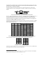
The ARM core runs on a clock known as the CCLK. How can we reliable measure the CCLK? We could
run a program on the core that toggles a pin, but there are too many settings influencing the result. So,
instead, we decided to try to get the CCLK on an external pin.
crystal
Fosc
CCLK ARM
core
PLL
APB
divider
LPC
PCLK
PWM
PWM
PWM
The three main frequencies (Fosc, CCLK and PCLK) and their relation.
As the figure above shows, the PLL generates the CCLK (core clock) from the crystal (Fosc). The PCLK
(peripheral clock) is derived from the CCLK with the so-called APB divider. The peripheral clock drives
many peripherals like the UARTs, the timers, etc. One peripheral in particular seems to suit our needs: the
PWM block. It is a hardware only block; once configured by software, it runs standalone.
2.2
The software
To drive the PWM we used the following code.
void pwm_init( void )
{
// We use P0.21/PWM5 as output pin
// Power the pwm block (note: it's on by default after reset)
PCONP |= 1<<5;
// Set the peripheral clock divider (to 1, so that PCLK=CCLK), VPBDIV is the APB divider
VPBDIV = 1; // 0 -> PCLK = 1/4 CCLK, 1 -> PCLK = 1/1 CCLK, 2 -> PCLK = 1/2 CCLK
// Configure pin (PWM5 is function 01)
PINSEL1 &= ~ ( 3<<10 );
PINSEL1 |=
( 1<<10 );
// Set the PWM prescaler (so that the PWM clock=PCLK=CCLK)
PWMPR = 0;
// Configure the PWM curve
PWMMR0 = 2; // Set PWM period to 2 PWM clock ticks
PWMMR5 = 1; // Flip line after 1 tick (so, we run at half the CCLK)
// Configure the PWM
PWMMCR = 0x00000002;
PWMPCR = 0x1<<13;
PWMLER = 0x7f;
block
// Reset TC on MR0
// Enable PWM5 (and set it to single edge)
// Latch 0 and 5
// Start PWM-ing
PWMPC = 0;
// Prescale counter to 0
PWMTC = 0;
// Reset timer to 0
PWMTCR = 0x09; // Enable PWM mode and start timer
}
Observe the following aspects of pwm_init():
•
We use PWM5 output via pin P0.21
•
The APB divider, known in Keil as VPBDIV, is set to 1
•
The PWM period is set to 2 PCLK ticks; the PWM output starts low, and after 1 tick the PWM output
is raised. Effectively, the PWM5 output runs at half the PCLK, and since the APB divider is 1, PWM5
runs at half the CCLK.
3
2.3
Startup
Our first measurement program is very simple: main() first calls the function pwm_init() from the previous
section, next it runs an infinite loop. See the code fragment below.
int main( void )
{
pwm_init();
while( 1 )
; // infinite loop
}
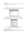
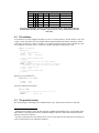
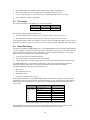
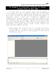
It should be noted that Keil’s uVision generates an assembler file that (to put it simply) maps the reset
vector to main(). This assembler file may also initialize the PLL, the MAM and some other things, but for
these performance experiments, we disabled that (see figure below).
Keil’s configuration wizard tab for startup.s (instead of text file tab), with most settings disabled
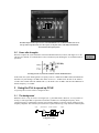
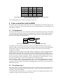
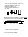
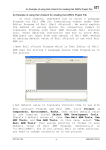
When one runs the program, and breaks it, a very nice feature of uVision is available in the menu
Peripherals | System Control Block | Phase Locked Loop 0. It is a dialog showing the current PLL settings
(and even allows one to make live changes).
PLL dialog from Keil’s uVision, showing the PLL is not enabled (top left checkbox labeled
PLLE). It also confirms the CCLK is 12 MHz (bottom line).
2.4
The practical results
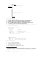
As the scope shows, at this high frequency, we do not get nice square pulses; there are ripples when
swinging low and there are ripples when swinging high. Nevertheless, we get 3 V pulses at a clear 6 MHz
pulse frequency. In other words, the CCLK is 12 Mhz.
4
The PWM output on the scope. The two vertical dashed lines are so-called track lines; the text at
the top of the scope shows they are 167 ns apart (so the pulse rate is 5.99 MHz). The black line
show the theoretical square pulses.
2.5
Some after thoughts
When we compare the crystal schematics of the Keil MCB2140 board (see below) with Figure 4-7 in the
LPC214x user manual, we conclude that we have a hardware layout matching the “b) oscillation mode of
operation”.
Zooming in on the crystal in the schematics of Keil’s MCB2140 board
In this mode, the crystal should generate a frequency between 1 MHz and 30 MHz. Indeed, the MCB2140
board has a crystal running at 12 MHz. This means we have Fosc=12 MHz. Since the PLL is not enabled,
CCLK is also 12 MHz. Since the APB divider is 1, the PLCK is also 12 MHz. And since the PWM runs at
half the frequency, it is 6 MHz.
3 Using the PLL to speed up CCLK
To speed up the CCLK we need to configure the PLL.
3.1
The background
Hardware-wise it is easy to divide a clock signal (see e.g. the APB divider). However, it is not possible to
multiply a clock signal. But it is possible to run another oscillator of a much higher frequency, whose
(output) frequency is automatically raised or lowered until it matches a reference (input) oscillator in both
frequency and phase. This control system is known as a phase-locked loop (“loop” from the feedback path).
input
phase detector variable oscillator
+
-
A diagram of a PLL
5
output
What does
this mean?
The figure above is a diagram of a PLL; it features one more element, namely a frequency divider in the
feedback path. This allows the output frequency to be a factor higher than the input frequency. So, with a
PPL and a divider, we implement a multiplier.
The LPC2148 features a PLL with two dividers, they are known as M and P. The so-called current
controlled oscillator (CCO) has a working range of 156 MHz to 320 MHz. The leads to the following
diagram.
Fosc
+
-
CCO
(156..320 MHz)
div by 2P
CCLK
div by M
The PLL in the LPC2148 with two dividers and a current controlled oscillator
Since the + input of the phase detector is 12 MHz, the – input should also be 12 MHz. By setting M to 1, 2,
3, 4, or 5 respectively, CCLK needs to be 12, 24, 26, 48, or 60 MHz respectively1 (60 MHz is the
maximum for the LPC2148). The trick is not in setting M, because that’s just a matter of picking the
wanted CCLK from the five possibilities. The trick is in selecting a P so that the CCO can operate in its
working range (156MHz..320MHz). P can only be 1, 2, 4, or 8.
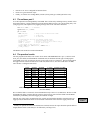
The table below shows which P we have to pick for the 5 CCLKs we can chose from (with Fosc=12 MHz).
The table also lists options for P in case Fosc would have been 10 MHz, just to illustrate that sometimes
there is more than one option for P.
Fosc
M
CCLK
FCCO
P=1
P=2
P=4
P=8
10
1
10
20
40
80
160
10
2
20
40
80
160
320
10
3
30
60
120
240
480
10
4
40
80
160
320
640
10
5
50
100
200
400
800
10
6
60
120
240
480
960
12
1
12
24
48
96
192
12
2
24
48
96
192
384
12
3
36
72
144
288
576
12
4
48
96
192
384
768
12
5
60
120
240
480
960
The M and P combinations where CCO is in its working range 156 MHz … 320 MHz (light gray)
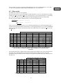
The bit fields MSEL and PSEL relate to dividers M and P according to the following table.
P
PSEL
M
MSEL
1
00
1
00000
2
01
2
00001
4
10
3
00010
8
11
4
00011
5
00100
Mapping of P and M to PSEL and MSEL bit fields
The PLLCFG register has MSEL in bits 0..4 and it has PSEL in bits 5 and 6. So, for our (12 MHz) board
the only legal values for PLLCFG are given in the table below.
The relation between Fosc, CCLK and M is CCLK = M × Fosc. Therefore, M is known as the multiplier.
Mathematically (functionally) this is true but technically, it is not.
1
6
Fosc = 12 MHz
CCLK M P
PSEL
MSEL
PLLCFG (bin)
PLLCFG (hex)
12
1
8
11
00000
110 0000
60
24
2
4
10
00001
100 0001
41
36
3
4
10
00010
100 0010
42
48
4
2
01
00011
010 0011
23
60
5
2
01
00100
010 0100
24
An overview of all possible values for CCLK, the associated values for M and P, the underlying
bit-fields MSEL and PSEL, the “complete” register PLLCFG (binary) and finally the PLLCFG
value in hex.
3.2
The software
To set the PLL, one must configure and enable it. Next, as a security measure2, the PLL must be “fed” with
“magic” values. This makes the CCO running, and the feedback path and the detector will tune it. It takes
some time before the PLL is stable (“locked”), so as a third step, the PLLSTAT must be checked for a lock.
If everything is ok, the PLL may be “connected”, and this must again be followed by a feed.
void pll_init( int cfg )
{
int loop_ctr;
// Step 1: Set CFG and CON
PLL0CFG
= cfg;
PLL0CON
= 0x01; // PLL Enable
// Step 2: Security measure: feed
pll_feed();
// Step 3: Wait for the lock into the new frequency
loop_ctr = 10000;
while( ((PLL0STAT&(1<<10))==0) && (loop_ctr>0) ) loop_ctr--;
// if PLL0STAT & (1<<10) does not hold, we have an issue...
// Step 4: Connect the PLL
PLL0CON |= 0x03;
// Step 5: Security measure: feed
pll_feed();
}
Where pll_feed() is defined3 as
static void pll_feed( void )
{
PLL0FEED = 0xAA;
PLL0FEED = 0x55;
}
The main() function now becomes:
int main( void )
{
pll_init(0x24); // legal values: 60, 41, 42, 23, 24
pwm_init();
while(1);
// infinite loop
}
3.3
The practical results
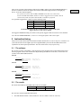
We run this program, checking pin P0.21 (PWM) on the scope. The practical results are as expected:
2
Quoting the user manual: “Since all chip operations, including the Watchdog Timer, are dependent on the
PLL0 when it is providing the chip clock, accidental changes to the PLL setup could result in unexpected
behavior of the micro controller”.
3
If you have interrupts active, this function is not correct: no bus operation may take place between the two
feeds, so interrupts have to be temporarily disabled.
7
PLLCFG
CCLK
Measured
CCLK from
passed to pll_init() in theory frequency measurement
24
60
30.1
60.2
23
48
24.1
48.2
42
36
18.0
36.0
41
24
12.0
24.0
60
12
5.99
12.0
The possible PLLCFG values, the theoretical resulting CCLK, the measured frequency,
and the associated practical CCLK.
So, by configuring the PLL, we achieve a speed-up of a factor of 5.
4 Faster code fetches with the MAM
We now know how to control the CCLK, and we have a way (PWM output pin) to actually measure it. The
next step is to measure execution speed of instructions. Since the ARM is pipelined, we would hope for one
instruction per CCLK tick.
4.1
The background
To execute instructions, they need to be fetched first. There are three possible routes. Firstly, an instruction
can come directly from the flash. Secondly, the MAM (memory acceleration module) might be enabled; it
pre-fetches instructions, speeding up the rather slow flash. Thirdly, the arm core may fetch instructions
from ram (if code happens to be located there).
Flash
MAM
ARM
core
RAM
The arm core and the three sources of an instruction (flash, MAM, RAM)
The address range 4000 0000 up to 4000 7FFF (32k bytes) and 7FD0 0000 7FD0 1FFF (8k bytes) are
mapped to RAM. So code fetches in these ranges are fetches from RAM. The address range 0000 0000 up
to 0007 FFFF (512k bytes) is mapped to flash. So code fetches in this range are fetches from flash,
optionally via the MAM.
The MAM is a sort of mini cache. It can either be disabled or enabled. If it is enabled, an instruction fetch
from the ARM is usually satisfied by the 128 bits (4 words, or 4 instructions) “pre-fetch buffer” in the
MAM. If the pre-fetch buffer does not contain the instruction, the ARM is stalled and the MAM fetches an
entire line of 128 bits into the pre-fetch buffer. Similarly, a data fetch causes the MAM to fetch an entire
line of 128 bits which is stored in “data buffer”. There is a third buffer, the “branch trail buffer”, also 128
bits, that is used when there is a break in the sequential flow of instruction fetches.
When the MAM is enabled, we have to configure how many CCLK ticks the MAM should use for flash
access. This register is known as MAMTIM and has values 1 up to 7. When MAMTIM is 1 the ARM core
runs at native speed. For high CCLK frequencies, MAMTIM must be greater than 1, because of the speed
limitations of the flash.
4.2
The software part 1
How do we measure the actual instruction speed? We decide to set and clear pin P1.16. We attach a scope
to that pin so that we can measure how fast it toggles. Note: a ‘toggle’ here means a full period of P1.16
first being low and next being high.
To be in full control of the instructions, we code them in assembler. We added the routine SBlink() to the
assembler file startup.s, which is already part of our project.
8
EXPORT
SBlink
SBlink
LDR R0, =0x00010000 ; mask for pin 16
LDR R1, =0xE0028010 ; base address of the slow GPIO port
SBlinkLoop
STR R0,[R1,#0x04] ; set port pin
NOP
NOP
NOP
NOP
NOP
NOP
NOP
NOP
NOP
STR R0,[R1,#0x0C] ; clear port pin
NOP
NOP
NOP
NOP
NOP
NOP
NOP
NOP
B SBlinkLoop
Observe the following points:
•
R0 is loaded with the mask for pin 16
•
R1 is loaded with the base address (E002 8010) of the slow SFRs controlling port 1
•
We first store R0 in R1+04 (so in E002 8014, or IO1SET) which raises P1.16
•
Later, we store R0 in R1+0C (so in E002 801C, or IO1CLR) which lowers P1.16 again.
•
At the end there is a (relative) jump back to the IOSET instruction.
• The NOPs are added to have some “meat” in the code4; the complete routine is now 20 instructions.
The main function now looks as follows
void SBlink( void ); // in assembler
int main( void )
{
pll_init(0x60);
pwm_init();
mam_init(4);
// 12MHz CCLK
// To check CCLK
// Init MAM
// Configure port P1.16 for slow general purpose output
SCS &= ~(1<<1);
// Select slow mode (for port 1)
PINSEL2 &= ~ (1<<3);
// Set port 1 (pins 16..25) to GPIO in one go
IODIR1 |= (1<<16);
// Set pin 16 for output
// Start blinking the slow I/O port
SBlink();
}
The used mam_init is new:
void mam_init( int
{
MAMCR = 0x00;
MAMTIM = cycles;
MAMCR = 0x02;
}
cycles )
// Disable the Memory Accelerator Module
// MAM fetch cycles
// Enable the Memory Accelerator Module
Observe the following points:
•
We run at the lowest CCLK of 12MHz.
•
We still enable the PWM to check the clock.5
•
The MAM is enabled (and set to 4 fetch cycles).
•
Port 1 is configured for slow (traditional, legacy) GPIO.
4
The MAM has a small buffer, so without any NOPs, the whole 3-instruction program would fit in the
MAM buffer. Secondly, as explained later, the STR instructions take unexpectedly many clock ticks.
Adding NOPs mitigates this somewhat.
5
As it appears later, the pwm_init() sets VPBDIV, and this also influences IO1SET and IO1CLR speed
(since slow I/O is done by a the GPIO peripheral on the APB bus).
9
•
Pins P1.16..P1.25 are configured for function GPIO.
•
Pin P1.16 is given direction output.
•
Finally, we call the never ending SBlink() routine (whose prototype is added just before main).
4.3
The software part 2
A second experiment is running SBlink() from RAM. This is achieved by declaring an array (named code in
the fragment below), copying sufficient bytes from function SBlink to array code, and executing array code
(using a typecast). This requires some juggling with type casts as the code below illustrates.
void SBlink( void ); // in assembler
typedef void(*func_t)(void);
int main(void)
{
char code[500];
pll_init(0x60);
pwm_init();
// Array to hold the SBlink code in RAM
// 12 MHz CCLK
// To check CCLK
// Configure port P1.16 for slow general purpose output
SCS &= ~(1<<1);
// Select slow mode (for port 1)
PINSEL2 &= ~ (1<<3);
// Set port 1 (pins 16..25) to GPIO in one go
IODIR1 |= (1<<16);
// Set pin 16 for output
// Copy SBlink to code, and run it
memcpy( (int*)code, (int*)&SBlink , sizeof(code) );
((func_t)code)();
}
The MAM is not needed for execution from RAM.
4.4
The practical results
The first program (from flash) is run 8 times. Seven times with MAMTIM from 1 up to 7, and once with
mam_init() not called (so with MAM left in disabled state, the hardware default). The second program
(from RAM) is run once. In each run, the time of one toggle on P1.16 is measured.6 The last column shows
the toggle time not in nano-seconds but in CCLK ticks (each of 83 ns, since the CCLK runs at 12 MHz,
since the PLL is configured with 0x60).
Code in
MAMCR
MAMTIM
T (toggle)
clock ticks @ 12 MHz
Flash
Disabled
N/A
13600 ns
163
Flash
Enabled
7
4080 ns
49
Flash
Enabled
6
3730 ns
45
Flash
Enabled
5
3410 ns
41
Flash
Enabled
4
3070 ns
37
Flash
Enabled
3
2980 ns
35
Flash
Enabled
2
2900 ns
35
Flash
Enabled
1
2820 ns
34
RAM
N/A
N/A
2810 ns
34
Time of one toggle on P1.16 (in nano seconds and in clock ticks) for different MAM settings
(CCLK is 12MHz).
We see that the flash is considerably slower than RAM: nearly a factor of 5 (13600/2810). We also see that
the MAM really helps in closing that gap (2820 ns versus 2810 ns). We also noticed that with the MAM
enabled, the predictability decreased: toggle periods differ in length.
Since the size of the code is 20 instructions, the (4 word) pre-fetch buffer should be reloaded 4 times per
toggle period (the branch trail buffer is also used due to the branch at the end of the toggle period). This
6
Actually two periods are measured (and that time is halved) because the scope shows that periods differ in
length (and one shorter seems always to be followed by one longer one).
10
Operational
model?
means a penalty of 4 ticks per increment of MAMTIM. We do see this for MAMTIM 4 to 5, 5 to 6, and 6
to 7. We can not explain the smaller penalty for MANTIM 1 to 2, 2 to 3, and 3 to 4.
4.5
Other results
We added some variation to the experiment.
The first variation was to increase the number of NOP instructions. As we see in the table below (compare
columns 2str+17nop+1b and 2str+18nop+1b), when going from 17 to 18 NOP instructions, we consistently
get 1 clock tick of extra time spent (for RAM and for flash through MAM with any timing setting).
We also reduced the number of NOPs to below 3 as in the code fragment below.
SBlinkLoop
STR R0,[R1,#0x04] ; set port pin
NOP
STR R0,[R1,#0x0C] ; clear port pin
NOP
B SBlinkLoop
In this case, the MAM buffers need never to be reloaded (presumably the pre-fetch buffer holds the first 4
and the branch trail buffer holds the last instruction), so the toggle period does not vary with the MAMTIM
setting. See the table below for measurements with 2 and 1 NOP in the code (compare 2str+2nop+1b with
2str+3nop+1b).
Time of one toggle (ns, clock ticks) – CCLK=12 MHz
Code
MAM
TIM
2str+1nop+1b
2str+2nop+1b
2str+3nop+1b
2str+17nop+1b
2str+18nop+1b
Flash
disabled
N/A
4540, 54
5100, 61
5700, 68
13600, 163
14400, 173
Flash
en
7
1505, 18
1585, 19
2180, 26
4080, 49
4180, 50
Flash
en
6
1505, 18
1585, 19
2095, 25
3730, 45
3830, 46
Flash
en
5
1510, 18
1575, 19
1995, 24
3410, 41
3540, 42
Flash
en
4
1505, 18
1575, 19
1910, 23
3070, 37
3160, 38
Flash
en
3
1505, 18
1580, 19
1815, 22
3005, 36
3080, 37
Flash
en
2
1510, 18
1575, 19
1775, 21
2900, 35
3010, 36
Flash
en
1
1505, 18
1575, 19
1675, 20
2820, 34
2940, 35
RAM
N/A
N/A
1505, 18
1580, 19
1665, 20
2810, 34
2890, 35
Time of one toggle on P1.16 for different MAM settings and various number of NOP instructions
(note ‘2str+3nop+1b’ stand for an SBlink() routine containing 2 store, 3 nop and 1 branch
instruction).
The second variation was to change the PLL setting so that we get a higher CCLK. See the table below for
the results. We see that the number of clock ticks remains the same. In other words, the real-world
performance increases linearly with the clock speed. Or, rephrased, the flash can keep up with the speed of
the ARM core.
Time of one toggle (ns, clock ticks) -- 2str, 17nop, 1b
Code
MAM
TIM
12MHz
36MHz
60MHz
Flash
disable
N/A
13600, 163
4610, 166
2750, 165
Flash
en
7
4080, 49
1355, 49
815, 49
Flash
en
6
3730, 45
1245, 45
750, 45
Flash
en
5
3410, 41
1135, 41
690, 41
Flash
en
4
3070, 37
1025, 37
620, 37
Flash
en
3
3005, 36
1005, 36
600, 36
Flash
en
2
2900, 35
975, 35
585, 35
Flash
en
1
2820, 34
945, 34
crash
RAM
N/A
N/A
2810, 34
945, 34
565, 34
Time of one toggle on P1.16 for different MAM settings and various CCLK speeds
11
Who can?
There is one exception: when running at full speed (60 MHz), and no waits in the MAM (MAMTIM=1),
the micro controller crashed. The surprise here is that crashes didn’t happen sooner (on all light gray
boxes). As the LPC manual explains:
For system clock slower than 20 MHz, MAMTIM can be 001. For system clock
between 20 MHz and 40 MHz, Flash access time is suggested to be 2 CCLKs, while in
systems with system clock faster than 40 MHz, 3 CCLKs are proposed.
If we put these suggestions in a table we get the following result.
CCLK
Suggested MAMTIM
Flash access time
10..20MHz
1
100ns..50ns
20..40MHz
2
100ns..50ns
40..60MHz
3
75ns..50ns
The MAMTIM setting from the LPC2148 manual for various CCLK speeds,
suggest a flash access time of 50 ns minimal
The suggested MAMTIM setting for various CCLK speeds, suggest a flash access time of 50 ns minimal.
So, in the test 60MHz/MAMTIM=1, we are over-clocking the system. This is out of spec!
5 Instruction timing
The previous section shows that a 20-instruction routine (known above as “2str+17nop+1b”) executes in 34
cycles instead of the 20 one might expect from a pipelined RISC processor like the ARM. This section
explains the less than expected performance. The next section shows a way to speed it up.
5.1
The software
We use three versions of the blinker: a base program, the base program with an extra STR instruction and
the base program with an extra B instruction. By measuring the difference in run-time, we know the cost
(in ticks) of the STR and B instruction.
2str+1b
SBlinkLoop
STR R0,[R1,#0x04] ; set port pin
STR R0,[R1,#0x0C] ; clear port pin
B SBlinkLoop
3str+1b
SBlinkLoop
STR R0,[R1,#0x04] ; set port pin
STR R0,[R1,#0x04] ; set port pin
STR R0,[R1,#0x0C] ; clear port pin
B SBlinkLoop
2str+2b
SBlinkLoop
STR R0,[R1,#0x04] ; set port pin
B SblinkLoopCont
SBlinkLoopCont
STR R0,[R1,#0x0C] ; clear port pin
B SBlinkLoop
5.2
The results
We run the three blinkers from RAM, with CCLK set to 12 MHz.
2str+1b
3str+1b
2str+2b
1420ns (17ticks)
1995ns (24ticks)
1670ns (20ticks)
Measuring individual instructions (slow GPIO)
We now have measured individual instructions:
•
The STR instruction takes 7 ticks (24 ticks for “3str+1b” minus 17 ticks for “2str+1b”)
12
Just luck?
•
The B instruction takes 3 ticks (20 ticks for “2str+2b” minus 17 ticks for “2str+1b”)
•
The NOP instruction takes 1 tick (35 ticks for “2str+18nop+1b” minus 34 ticks for “2str+17nop+1b”;
see previous chapter)
These timing figures explain to the digit the timing results of the previous chapter: 2str+17nop+1b runs in
2×7 + 17×1 + 1×3 = 14 + 7 + 3 = 34 cycles.
5.3
More results
It suddenly struck us that slow GPIO runs on the ARM peripheral Bus (APB). The APB bus runs on the
PCLK, which is derived from CCLK via the APB divider. The controlling SFR VPBDIV is set to 1 in
pwm_init(). We decided to rerun the three tests, with varying PCLKs.
2str+1b
3str+1b
VPBDIV=1 (PCLK=1/1×CCLK=12MHz)
1420ns (17ticks)
1995ns (24ticks)
VPBDIV=2 (PCLK=1/2×CCLK=6MHz)
1820ns (22ticks)
2660ns (32ticks)
VPBDIV=0 (PCLK=1/4×CCLK=3MHz)
2980ns (36ticks)
4315ns (52ticks)
Measuring individual instructions (slow GPIO) with varying PCLK
When we look at the STR instruction we see that the STR instruction takes 24-17=7 ticks when the APB
divider is 1, that it takes 32-22=10 ticks when the APB divider is 2 and that it takes 52-36=16 ticks when
the APB divider is 4.
We can explain this by assuming that the STR instruction takes 4 internal ARM core cycles and 3 APB bus
cycles. When the APB divider is 1, we get 4+3=7, when the APB divider is 2 we get 4+2×3=10 and when
the APB divider is 4, we indeed get 4+4×3=16.
6 Using fast GPIO instead of slow GPIO
We now know that the STR instruction for the slow GPIO SFRs takes 7 ticks (when PCLK=CCLK). We
expected 1 tick, so that is indeed slow. How much faster would the new “fast” GPIO be? We repeat the
experiment of the previous chapter, now with fast GPIO.
6.1
The software
The main() function changes slightly; we have to set up P1.16 for fast GPIO.
void FBlink( void ); // in assembler
int main(void)
{
char code[500];
// Array to hold the FBlink code in RAM
pll_init(0x60);
// 12MHz CCLK
// Configure port P1.16 for fast general purpose output
SCS |= 1<<1;
// Select fast mode (for port 1)
PINSEL2 &= ~ (1<<3);
// Set port 1 (pins 16..25) to GPIO in one go
FIO1MASK &= ~(1<<16);
// Enable pin for set/clear
FIO1DIR |= (1<<16);
// Set pin for output
// Copy FBlink to code, and run it
memcpy( (int*)code, (int*)&FBlink , sizeof(code) );
((func_t)code)();
}
We also have to write FBlink (in assembler startup.s) to use the fast SFR’s instead of the slow SFR’s.
EXPORT
FBlink
FBlink
LDR R0, =0x00010000 ; mask for pin 16
LDR R1, =0x3FFFC020 ; base address of the fast GPIO port
FBlinkLoop
STR R0,[R1,#0x18] ; set port pin
STR R0,[R1,#0x1C] ; clear port pin
B FblinkLoop
Note
13
Who knows
about the
ARM/LPC
interaction?
•
R1 is loaded with the base address (3FFF C020) of the fast SFRs controlling port 1
•
We first store R0 in R1+18 (so in 3FFF C038, or FIO1SET) which raises P1.16
•
Later, we store R0 in R1+1C (so in 3FFF C03C, or FIO1CLR) which lowers P1.16 again.
•
At the end there is a (relative) jump back.
6.2
The results
We run the three blinkers from RAM, with CCLK set to 12 MHz.
2str+1b
3str+1b
2str+2b
585ns (7ticks)
755ns (9ticks)
840ns (10ticks)
Measuring individual instructions (fast GPIO)
We now have measured individual instructions:
•
The STR instruction takes 2 ticks (9 ticks for “3str+1b” minus 7 ticks for “2str,+1b”)
• The B instruction still takes 3 ticks (10 ticks for “2str+2b” minus 7 ticks for “2str+1b”)
The conclusion is that a STR to slow GPIO is 3.5 times as slow as an STR to fast GPIO (7 ticks versus 2), 5
times as slow (10 ticks versus 2) or even 8 times as slow (16 ticks versus 2) depending on the APB divider.
6.3
Some final theory
The LPC2148 contains an ARM7TDMI-S core. As the ARM7TDMI-S reference manual explains that this
core uses a pipeline to increase the speed of the flow of instructions. This allows several operations to take
place simultaneously, and the processing, and memory systems to operate continuously. A three-stage
pipeline is used, so instructions are executed in three stages:
•
Fetch (the instruction is fetched from memory)
•
Decode (the registers used in the instruction are decoded)
• Execute (registers are read from register bank, the ALU operates, and the registers are written back)
The ARM7TDMI-S has a “Von Neumann” architecture, with a single 32-bit data bus carrying both
instructions and data. Only load, store, and swap instructions can access data from memory.
The ARM7TDMI-S has four basic types of memory cycle:
•
Idle cycle (I)
•
Non-sequential cycle (N)
•
Sequential cycle (S)
• Coprocessor register transfer cycle (C)
In the pipelined architecture of the ARM7TDMI-S, while one instruction is being fetched, the previous
instruction is being decoded, and the one prior to that is being executed. The table below (taken from the
ARM manual) lists the number of cycles required by an instruction, when that instruction reaches the
execute stage.
Instruction
Qualifier
Cycle count
Any unexecuted
Condition codes fail
+S
Data processing
Single-cycle
+S
B, BL
-
+N +2S
STR
-
+N +N
SWP
-
+N +N +I +S
MCR
-
+(b)I +C +N
… more …
Excerpt from the timing table from ARM7TDMI-S reference manual
We see that a B instruction has a fetch, decode, non-sequential, sequential, and sequential cycle. The
ARM7TDMI-S reference manual explains the operations in the three execute steps:
14
1.
During the first cycle, a branch instruction calculates the branch destination while performing a prefetch from the current PC. This pre-fetch is done in all cases because, by the time the decision to take
the branch has been reached, it is already too late to prevent the pre-fetch.
2. During the second cycle, the ARM7TDMI-S performs a Fetch from the branch destination.
3. During the third cycle, the ARM7TDMI-S performs a Fetch from the destination.
The STR instruction has a fetch, decode, non-sequential, and non-sequential cycle. The ARM7TDMI-S
reference manual explains the operations in the two execute steps:
1. During the first cycle, the ARM7TDMI-S calculates the address to be stored.
2. During the second cycle, the ARM7TDMI-S performs the base modification, and writes the data to
memory (if required).
7
0
STR
STR
B
STR
STR
B
STR
1
F
2
3
4
5
7
6
7
8
9 10 11 12 13 14 15 16 17 18
D XN XN
F D
XN XN
F D
XN XS XS
F D XN XN
F D
XN XN
F D
XN XS XS
F D XN XN
The timing of the fast GPIO loop (bounded by the execution phase) is indeed 7 ticks
The figure above illustrates the timing of the fast GPIO loop.
For slow GPIO, the STR takes 7 cycles instead of 2. This has to do with the slow GPIO going through the
ARM Peripheral Bus. An explanation would be that each N access does have a wait state introduced by the
AHB wrapper, and that there is an additional wait of 3 APB clocks (see figure below). This results in a 7
clock execute phase (as measured). Furthermore, it also explains why an APB divider set to 2 makes the
execute phase of the store last 4+2×3=10 ticks.
17
0
STR
STR
B
STR
1
F
2
3
4
5
6
7
8
9
10
11
12
13
14
15
16
17
D X1N ws APB APB APB X2N ws
F
D
X1N ws APB APB APB X2N ws
F
D
XN XS
F
18
19
20
21
22
XS
D X1N ws APB APB
A possible explanation of the timing of the slow GPIO loop
7 Conclusions
7.1
Performance
We have looked at several aspects of tuning the system for performance.
•
The PLL allows us to boost an external clock with a minimum frequency of 10MHz to 60MHz. A
speed-up of a factor of 6 (our board had a crystal of 12MHz, not 10MHz).
•
With an enabled MAM with minimal timing (or when running from RAM) we get a speedup of nearly
5 with respect to running from flash directly.
•
Fast GPIO is 3.5 times (or 5 or 8 times) as fast as slow GPIO (depending on the APB divider).
Total speedup achieved is 6 × 4.8 × 8 = 230.4.
So, the system’s performance window (for GPIO) is a factor 230 wide.
15
Confirmation?
7.2
Theory
We now understand the purpose and architecture of the PLL in the system, namely multiplying the external
clock. The details of choosing an oscillator are not yet clear.
We understand the purpose of the MAM in the system, namely bridging the speed gap between the flash
and the ARM core. The details of the timing and the purpose of the three buffers is not completely clear.
We have seen that code in RAM performs optimally.
We have seen that STR instructions to slow GPIO SFRs perform really poor (non sequential accesses
delayed by the APB bus), and that STR instructions to fast GPIO performs much better. The slow GPIO is
even slower when the APB divider kicks in.
The details of why each instruction clocks as measured are not yet completely understood, but the theory
roughly matches the practice.
7.3
Future work
We used 32 bits ARM instructions. As a future step we could check the thumb instructions.
(end of doc)
16