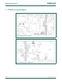
1
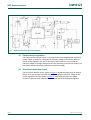
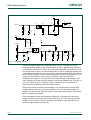
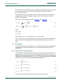
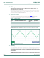
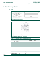
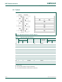
UM10321
75 W SSL1750 triac dimmable 230 V mains LED driver
Rev. 01 — 9 October 2009
User manual
Document information
Info
Content
Keywords
SSL 1750, PFC, LED driver, high power, triac, high power factor, mains
dimmable
Abstract
User manual for the SSL1750 230 V(AC) mains dimmable 75 W, 1000 mA
LED driver board.
UM10321
NXP Semiconductors
SSL1750 triac dimmable LED driver
Revision history
Rev
Date
Description
01
20091009
Initial release
Contact information
For more information, please visit: http://www.nxp.com
For sales office addresses, please send an email to: [email protected]
UM10321_1
User manual
© NXP B.V. 2009. All rights reserved.
Rev. 01 — 9 October 2009
2 of 24
UM10321
NXP Semiconductors
SSL1750 triac dimmable LED driver
1. Introduction
This SSL1750 board is a 75 W, 1000 mA current regulated, LED driver that is dimmable
with standard mains triac dimmers. The board is using the NXP SSL1750 switched mode
power supply with integrated power factor correction (PFC) and flyback controller. The
circuitry for communication between both controllers is integrated and needs no
adjustment. The PFC output power is on-time controlled for simplicity. It is not necessary
to sense the phase of the mains voltage. The flyback output-power is current-mode
controlled for good suppression of input-voltage ripple.
The board is very efficient, higher than 85 %, has a high power factor, above 0.95 over the
whole voltage input range and the THD falls within the limits for class-C equipment.
Making this board ideal for dimmable high power LED lighting systems.
The board has been optimized for triac-based dimmers. As different triac dimmers have
different specifications the dimming performance of the reference board might vary based
on the used dimmer. Transistor dimmers and other non-triac dimmers will not work with
this board.
1.1 IC description
The SSL1750 is a Switched Mode Power Supply (SMPS) controller IC, suitable for driving
LED applications from 25 W up to 250 W. For LED power requirements below 25 W the
NXP SSL210x family is preferred.
The SSL1750 combines Power Factor Correction (PFC) and a flyback controller. Its high
level of integration allows the design of a cost-effective high efficiency LED power supply
with a low number of external components.
The special built-in green functions provide high efficiency at all power levels. This applies
to quasi-resonant operation at high power levels, quasi-resonant operation with valley
detection, as well as reduced frequency operation at lower power levels. At low power
levels, the PFC switches over to burst mode control to maintain high efficiency. In burst
mode, soft-start and soft-stop functions are added to eliminate audible noise.
During low power conditions, the flyback controller switches to frequency reduction mode
and limits the peak current to 25 % of its maximum value. This will ensure high efficiency
at low power while minimizing audible noise from the transformer.
The proprietary high voltage BCD800 process makes direct start-up possible from the
rectified universal mains voltage in an effective and green way. A second low voltage
Silicon On Insulator (SOI) IC is used for accurate, high speed protection functions and
control.
The SSL1750 enables the design of highly efficient and reliable LED drivers at power
requirements up to 250 W, it can be designed with a minimum number of external
components.
UM10321_1
User manual
© NXP B.V. 2009. All rights reserved.
Rev. 01 — 9 October 2009
3 of 24
UM10321
NXP Semiconductors
SSL1750 triac dimmable LED driver
2. Specification
The main specification is given in Table 1
Table 1.
Specification for the SSL1750 dimmable board
Type
Value
AC line input voltage
230 V ± 10 %
DC Output current
1000 mA ± 10 %
When not dimmed
Output Power
75 W ± 10 %
When not dimmed
DC Output Voltage
56 V to 82 V
Depending on LED forward voltage.
Dimming range
100 mA to 1000 mA
Depending on dimmer.
Driver Efficiency
> 85 %
Over whole input voltage range.
With 75 W load and no dimming
Power Factor
> 0.95
For 230 V (AC) ± 10 % mains and no dimmer
used
Fig 1.
Comment
Photo of the dimmable 75 W LED driver board
3. Board connections
3.1 Input
On the AC input, connector X1, you can connect 230 V (AC) (± 10 %) 50 Hz. The mains
can be connected to the board directly or via a triac dimmer. See Section 5.4 for more
details about the different dimmers.
3.2 Output
The anode of the LED strings should be connected to the '+' of connector X2. The cathode
should be connected to the '-' of the same connector.
The board is designed to provide 1000 mA of current into a LED load. It is advised to use
only one LED string. When more than one LED string is used, care must be taken to
balance the current in each string to prevent one LED string having higher currents than
other strings. In Table 2 example configurations are listed of different LED loads.
UM10321_1
User manual
© NXP B.V. 2009. All rights reserved.
Rev. 01 — 9 October 2009
4 of 24
UM10321
NXP Semiconductors
SSL1750 triac dimmable LED driver
The total forward voltage (VF) of the LED string should not exceed the maximum output
voltage of the board (see Section 4.5.2). A lower total VF is allowed, as long as the output
stays above the minimum output voltage (see Section 4.5.1).
Table 2.
Example of LED configurations
Current per led string
(mA)
LED strings
Number of LEDSs
per string
VF
(V)
330
3
24
3.15
500
2
23
3.25
1000
1
22
3.4
4. Functional description
The board is made around the SSL1750 IC. The SSL1750 includes a PFC and a flyback
controller integrated in one SO-16 package.
The PFC boost the rectified mains voltage to 380 V, which is enough to have a excellent
power factor up to 250 V (AC) input. The PFC output power is on-time controlled for
simplicity. It is not necessary to sense the phase of the mains voltage. During low dimming
levels the PFC will go into burst mode for higher efficiency.
The board act as a current source for the LED load. The board can be used with and
without a dimmer. Without a dimmer the driver will supply 1000 mA of current. With a
dimmer the current depends on the phase cut angle of the dimmer. The phase cut signal
of a dimmer is converted into a reference voltage so that the phase cut signal determines
the level of the output current. The output current is analog regulated which means that no
Pulse With Modulation (PWM) is used.
A simplified functional application diagram is shown in Figure 2. Besides the PFC and
flyback, a bleeder, an output current regulation and a dimming phase-angle detection
circuit are shown. The function of these circuits are explained in this chapter.
UM10321_1
User manual
© NXP B.V. 2009. All rights reserved.
Rev. 01 — 9 October 2009
5 of 24
UM10321
NXP Semiconductors
SSL1750 triac dimmable LED driver
Fig 2.
Simplified functional application diagram
4.1 Output current regulation
The output current is sensed with a (1 Ω) sense resistor and compared with a reference
voltage. When no dimmer is connected, the reference voltage is such that a 1000 mA
current will be supplied to the load on the output. When a dimmer is connected the
reference voltage will change and thus the current, depending on the dimmer setting. The
triac phase detection circuit will generate this reference voltage.
4.2 Triac phase detection circuit
The triac phase detection circuit, shown in Figure 3, detects the phase angle of the triac
dimmer to be able to control the LED current by changing the reference voltage for the
current regulation loop. Also shown in Figure 3, is the feedback loop to the flyback
controller. A gamma curve is build-in to have a linear perceived-brightness response.
UM10321_1
User manual
© NXP B.V. 2009. All rights reserved.
Rev. 01 — 9 October 2009
6 of 24
UM10321
NXP Semiconductors
SSL1750 triac dimmable LED driver
VCC
B2
VB2
FBCTRL
2
2
R26
39 kΩ
LMV710
33 Ω
BAS29
Rsense
R58
4
V−
Vref
10 kΩ
R76
1 kΩ
C20
10 nF
VDC
V22
R30
120 Ω
HCPL817
C19
330 nF,
16 V
R50
R56
4.7 kΩ
V+
A3
3
5
1
C32
R37
22 nF
10 kΩ
VCC
C30
47 μF,
50 V
Vbridge
R40
4.7 kΩ
1
R39
1 MΩ
C
B
R43
33 kΩ
Fig 3.
V18
15 V
R57
1 MΩ
4
3 VB3
2
V17
BC846
E
B3
HCPL817
R42
10 kΩ
V24
R45
BAS70
470 kΩ
C27
100 nF
R46
680 kΩ
V34
DNP
C33
100 nF
C34
330 nF,
16 V
R47
1 MΩ
Triac phase detector
The dimmer signal is taken from the bridge rectifier (Vbridge). Transistor V17 will be
conducting when a voltage on the mains is detected (> 50 V). When the triac dimmer is
not conducting, transistor V17 will be off. Via the opto-coupler, B3, the capacitor C27 will
be charged when the triac is on. When the dimmer is at 100 % conducting capacitor C27
is fully charged and diode V24 is not conducting. The resistive divider R57, R46, R45 and
R47 will set the voltage level on the inverting input (pin 4) of the error amplifier A3. This
voltage sets the maximum current. When the dimmer is set to less than 100 %
conducting, the voltage on C27 drops and V24 conducts therefore the voltage on C33
drops. Resulting in a lower reference voltage for the current feedback loop. There the V-I
curve of the diode (V24) is of logarithmic nature, the dimming curve will also be of
logarithmic nature resulting in the desired gamma curve.
Diode V24 is chosen so that its forward voltage is low. This prevents a too high offset
voltage needed at the non-inverting error amplifier input. Also the diode temperature
behavior can influence the reference voltage. A low leakage Schottky type, like the NXP
BAS70, is therefore preferable.
The error amplifier is build with operational amplifier A3. It compares the input sense
voltage measured across the sense resistors (R66, R70, R72, R73) with the reference
voltage. An opto-coupler is directly connected to the flyback control input FBCTRL to
control the flyback frequency and mode.
UM10321_1
User manual
© NXP B.V. 2009. All rights reserved.
Rev. 01 — 9 October 2009
7 of 24
UM10321
NXP Semiconductors
SSL1750 triac dimmable LED driver
The resistive divider formed by R30 and R65 sets an offset voltage on the current sense
input. This makes sure that the load current can be controlled down to zero. The offset
voltage corresponds with the minimum voltage present at the inverting input of the error
amplifier when the dimmer conducting phase is set to maximum.
The power supply for error amplifier A3, shown in Figure 4, is formed by use of an
accurate reference voltage (TL431).
VCC
8
V19
1
C
BAS29
2
7
E
V20
R48
4.7 kΩ
B BC846B
1
2
R54
10 kΩ
1
1
C29
10 μF,
63 V
1
A4
C37
10 μF,
63 V
8
TL431ACD
2
7
6
3
2
2
R55
10 kΩ
2
1
Fig 4.
Power supply circuit for the error amplifier
4.3 Bleeder
To be able to work with a large range of dimmers a bleeder circuit is included on the board
to provide a load for the dimmer to reset the dimmer timer and provide latch current for the
dimmer triac.
In Figure 5 the bleeder circuit diagram is shown. The FET, V28, operates as a current
source. The current, Ibleeder, through R65 depends on the gate voltage which is set by the
zener diode:
V zener – V th
8.2 – 4.5
I bleeder = --------------------------- = --------------------- = 112mA
33
R 65
(1)
The bleeder current will only flows when the bridge voltage Vbridge is below the level set by
R59, R102, R107, R61 and VBE of transistor V29.
UM10321_1
User manual
© NXP B.V. 2009. All rights reserved.
Rev. 01 — 9 October 2009
8 of 24
UM10321
NXP Semiconductors
SSL1750 triac dimmable LED driver
VBridge
R59
330 kΩ
R60
330 kΩ
R102
330 kΩ
R103
330 kΩ
R107
330 kΩ
R105
330 kΩ
I bleeder
V28
STP5NK50Z
V30
8.2 V
R61
10 kΩ
Fig 5.
R65
33 Ω, 1 W
R62
2.2 kΩ
Bleeder circuit diagram
4.4 Flyback shut down circuit
At the lowest dimming settings the average input voltage is too low for the PFC to operate.
The PFC-converter turns off and as a consequence the SSL1750 chip enters in the start
up sequence. This causes interruptions in the output current, which are visible as flicker in
the LED's.
Figure 6 shows the circuit used to switch off the flyback controller to prevent flickering
dimming when the input voltage is too low.
Vbridge
FBCTRL
V36
R97
V37
1 k, 1W
BYW56
R90
PMLL4448
1 k, 1W
R91
820 kΩ
R92
2 kΩ
R93
1 MΩ
C
B
C40
10 μF,
400 V
E
C
B
V39
BC846B
V40
BC846B
E
R96
2.2 kΩ
Fig 6.
Flyback shutdown circuit diagram
Transistor V39 will pull FBCTRL to ground when the mains input voltage is below the
lower trip level, causing the flyback to switch off. The input voltage from the bridge rectifier
is detected by V37 and C40. The circuit inhibits an hysteresis. The hysteresis prevents the
LED-driver from oscillating. The combination of R96 and R91 determines the lower trip
level, V36 and R96 in parallel combined with R91 determines the higher trip level.
UM10321_1
User manual
© NXP B.V. 2009. All rights reserved.
Rev. 01 — 9 October 2009
9 of 24
UM10321
NXP Semiconductors
SSL1750 triac dimmable LED driver
The lower trip level must be chosen in such a way that it corresponds with the level of the
AC input voltage (output of the dimmer) just slightly above the point at which the
PFC-converter turns off.
The higher trip level must be chosen in such a way that the FBCTRL level is open just
below the minimum AC input voltage so that the driver is able to switch on under all
allowed mains conditions.
The levels can be calculated as shown in Equation 2: and Equation 3
R 91 + R 96
1
V low ( RMS ) = ------- × V BE × ----------------------R 96
2
(2)
R 91
R 91
1
V high ( RMS ) = ------- ⎛ V BE ⋅ ------- + ( V BE – V F ) ⋅ ------- + V BE⎞⎠
⎝
R 96
R 92
2
(3)
Where:
VBE = 0.63 V
VF = 0.56 V
The board is set at Vlow = 165 V RMS and Vhigh = 185 V RMS.
Due to voltage spikes, from switching-on the triac during dimming, the actual point could
differ in some cases. Decreasing the value of capacitor C40 may help to reduce this
effect.
4.5 Protections
The board and IC have several protections. In the following sections the main protections
are mentioned. For details on protections in the IC please see the data sheet of the
SSL1750 IC.
4.5.1 Output under voltage protection
The output under voltage is detected by the Vth(UVLO) on the VCC pin. When the VCC level
falls below the Vth(uvlo) level of 15 V (± 1 V) the flyback will be switch off. The VCC level
depends on the output voltage. Therefore the protection will kick-in when the total forward
voltage of the LED load is below Ns/Naux x Vth(UVLO). Where Ns is the number of secondary
turns and Naux is the number of auxiliary turns of the transformer.
Ns
V o ( UVLO ) = ----------- × V th ( UVLO )
N aux
(4)
28
V o ( UVLO ) = ------ × 15 = 52.5V ( typ )
8
(5)
28
V o ( UVLO ) = ------ × 14 = 49V ( min )
8
(6)
28
V o ( UVLO ) = ------ × 16 = 56V ( max )
8
(7)
Resulting in a minimum total forward voltage of the LED load to be 56 V.
UM10321_1
User manual
© NXP B.V. 2009. All rights reserved.
Rev. 01 — 9 October 2009
10 of 24
UM10321
NXP Semiconductors
SSL1750 triac dimmable LED driver
4.5.2 Output over voltage protection
The output Over Voltage Protection (OVP) is provided by detecting the output voltage by
the FBAUX pin. The FBAUX pin is connected via RFBAUX to the auxiliary winding.
Ns
V o ( ovp ) = ----------- ( I ovp ( FBAUX ) × R FBAUX + V clamp ( FBAUX ) )
N aux
(8)
Ns
V o ( ovp ) = ----------- ( 300μ × 82K + 0.7 ) = 88.6V ( typ )
N aux
(9)
Ns
V o ( ovp ) = ----------- ( 279μ × 82K + 0.7 ) = 82.5V ( min )
N aux
(10)
Ns
V o ( ovp ) = ----------- ( 321μ × 82K + 0.7 ) = 94.6V ( max )
N aux
(11)
Where Ns is the number of secondary turns and Naux is the number of auxiliary turns of the
transformer. The value of RFBAUX can be adjusted to the turns ratio of the transformer,
thus making an accurate OVP detection possible.
To restart after an over voltage event, interrupt the mains to reset the internal latch.
4.5.3 PFC bus voltage protection
In case of an over voltage on the PFC bus, the PFC-controller will stop operating.
4.5.4 Temperature protection
The IC does have an internal temperature protection. When the internal temperature is
above typical 140 °C the IC switches off to protect itself and the application.
A Negativice Temperature Coefficent (NTC) device could be placed on the board, which
should be connected to the latch pin, to shutdown the circuit if the ambient temperature is
too high.
5. Measurements
5.1 Power Factor Correction (PFC)
Due to the integrated PFC controller the board will have a power factor above 0.95 for
mains of 230 V (AC) ± 10 %. Table 3 gives the actual values. Measurements were
executed under full load (75 W).
Table 3.
Power factor versus mains voltage (50 Hz mains)
Mains V (AC) RMS
Power factor
207
0.979
220
0.975
230
0.971
240
0.965
245
0.960
250
0.956
253
0.957
UM10321_1
User manual
© NXP B.V. 2009. All rights reserved.
Rev. 01 — 9 October 2009
11 of 24
UM10321
NXP Semiconductors
SSL1750 triac dimmable LED driver
5.2 Efficiency
Without a dimmer, the board can reach an efficiency of 85 % with 230 V (AC) ± 10 %
while delivering 75 W of output power.
The efficiency of the board varies with the dimming level. Measurements with 3 different
dimmers showed efficiency from 55 % at the lowest dimming position, up to 85 % at full
power. This includes the losses in the dimmer
5.3 Harmonic currents
The harmonic currents measured on the board are listed in Table 4. The harmonic
currents for this board are below the limits of the Class-C of IEC 61000-3-2.
Table 4.
Harmonic currents
Harmonic
order
Maximum permissible harmonic
percentage of fundamental current
Measured
current [A]
Measured
percentage
1
-
0.368
-
3
30 x PF (= 28.7 %)
0.100
27.1 %
5
10 %
0.013
3.7 %
7
7%
0.014
3.9 %
9
5%
0.006
1.6 %
Remark: Measurement conditions: VI = 231 Vpac; PI = 85 W; I = 0.384 A; pf = 0.956
lmains
Fig 7.
Mains current 230 V version
5.4 Dimming
The board has been optimized for triac-based dimmers. Several triac dimmers have been
tested by NXP Semiconductors. As different dimmers have different specifications the
dimming performance of the reference board might vary based on the used dimmer.
Non-triac dimmers, like transistor dimmers or so called electronic dimmers, are not tested
with this board.
Remark: Non-triac dimmers, like transistor dimmers or so called electronic dimmers, have
not been tested with this board
UM10321_1
User manual
© NXP B.V. 2009. All rights reserved.
Rev. 01 — 9 October 2009
12 of 24
UM10321
NXP Semiconductors
SSL1750 triac dimmable LED driver
5.4.1 Dimming curve
Measurement data of the dimming curve, as described in Section 4.2, is shown in
Figure 8
1000
Output current
(mA)
800
600
400
200
0
0.0
2.0
4.0
6.0
8.0
10.0
ton dimmer (50 Hz)
Fig 8.
Dimming curve; triac on time (Ton, ms) versus output current (50 Hz system)
When the dimming level is getting below a certain point (Ton ~2 ms), the input voltage
seen by the board, will be too low and the board will switch off the flyback.
UM10321_1
User manual
© NXP B.V. 2009. All rights reserved.
Rev. 01 — 9 October 2009
13 of 24
xxxx xxxxxxxxxxxxxxxxxxxxxxxxxxxxxx x xxxxxxxxxxxxxx xxxxxxxxxx xxx xxxxxx xxxxxxxxxxxxxxxxxxxxxxx xxxxxxxxxxxxxxxxxxxxxx
xxxxx xxxxxx xx xxxxxxxxxxxxxxxxxxxxxxxxxxxxx xxxxxxxxxxxxxxxxxxxxxx xxxxxxxxxxx xxxxxxx xxxxxxxxxxxxxxxxxxx
xxxxxxxxxxxxxxxx xxxxxxxxxxxxxx xxxxxx xx xxxxxxxxxxxxxxxxxxxxxxxxxxxxxxxx xxxxxxxxxxxxxxxxxxxxxxxx xxxxxxx
xxxxxxxxxxxxxxxxxxxxxxxxxxxxxxxxxxxxxxxxxxxxxx xxxxxxxxxxx xxxxx x x
1 L2 4
3
S
Fig 9.
2
1
1
2
+ C29
10 μF,
63 V
1
2
R55
10 kΩ
2
5
R30
2
1 R37 2
10 kΩ
VCC
2
X5
4
Vgate
VB2
6
5
Rsense
VB3
header 3 × 2
3
Vref
Y4
1
Y5
2
3
C32
1 2
22 nF
heatsinkSSL1750
heatsinkSSL1750
2
R43
33 kΩ
Circuit diagram of the 75 W mains dimmable LED driver board 230 V (AC); 50 HZ version
2
1
V34
DNP
C33
100 nF
1
C34
330 nF,
16 V
R47
1 MΩ
2
1
R46
680 kΩ
1
C27
100 nF
2
1
R42
10 kΩ
R45
470 kΩ
BAS70
2
V17
BC846B
R57
1 MΩ
2
1
R77
V24
2
1
2
VB3
2
2
C
1
B
1
1
4
3
2
B3
1
2
R40
4.7 kΩ
HCPL817
V18
15 V
1
Rsense
R58
10 kΩ
1
2
R76
1 kΩ
1
12
1
2
C41
470 nF,
16 V
1 120 Ω 2
2
1
1
2
3
1
R56
47 kΩ
VCC
R101
330 kΩ
1
2
2
10 kΩ
1
G
2
1
1
2
HCPL817
1
C30 +
47 μF, 50 V
1
C
V22
BAS29
1 R94 2
R95
1 kΩ
1
1
1
2
2
1 1
2
2
33 Ω
VINSENSE
E
V39
BC846B
Vgate
1Ω, 1W
VCC
A4
8
V+ 3
+
1 VB2 1 R75 2
1
- 4
2
LMV710
V-
1
1
2
2 R50 1
C19
330 nF,
16 V
B
2
R96
2.2 kΩ
V40
BC846B
E
C
B
B
C
2
1
2
R91
270 kΩ
V38
BC846B
B2
4
3
R39
330 kΩ
2 R88 1
1 kΩ
V32
DNP
2
VCC
R23
82 kΩ
VDC
2
1
1
12
+
1
PMLL448
R92
2 kΩ
7 6 3
1000 pF,
440 V / Y1
2
C40
10 μF, 400 V
1 2
1
V30
8.2 V
R65
33 Ω, 1 W
2
1
1
2
R62
2.2 kΩ
2
12
12
12
D
S
V29
BC846B
2
V36
R73
2
2
R26
39 kΩ
R89
100 kΩ
R93
330 kΩ
R106
270 kΩ
V28
STP5NK50Z
G
330 kΩ
R104
270 kΩ
1 kΩ, 1W
C 2
1 E
2
2
R103
330 kΩ
330 kΩ
C15
1 μF,
50 V
FBCTRL
C20
10 nF
1
D
R54
10 kΩ
1
TL431ACD
C16
220 pF,
7
630 V ISE900019410
2
1
1
2
1
+ C14
47 μF,
50 V
330 kΩ
1 R90 2
+ C37
10 μF,
63 V
FBAUX
1 R99 2 1 R100 2
1 kΩ, 1W
R48
4.7 kΩ
VCC
R33
10 kΩ
1Ω, 1W
2
S
UM10321
14 of 24
© NXP B.V. 2009. All rights reserved.
1
1 R97 2
1
V14
BAS29
HVS2(NC)
SSL1750T
E
1
1
1 2
1 2
2
B
V37
BYW56
R105
330 kΩ
R107
330 kΩ
R61
10 kΩ
2
8
2
SSL1750 triac dimmable LED driver
R102
330 kΩ
R60
330 kΩ
6
R72
2
3
2
V15
24 V
1 R98 2
R59
330 kΩ
1
R19
47 Ω
1
GND
1
E
R29
t˚
DNP
R17
2
1
C25
470 nF,
16V
C23
10 nF
12
1
2
1
1
4
R82
2.2 kΩ
2
5
1
R28
33 kΩ
HVS1(NC)
R70
V20
BC846B
C
E
VDC
1
15
7
1
C39
1 2
HV
2
1
LATCH
2
1Ω, 1W
V19
+
OUT
-
1
16
FBSENSE
1
6
R20
2 1 kΩ 1
FBDRIVER
1
10
VOSENSE
2
2
1
2
R31
120 kΩ
8
14
1
2
1
2
V27
3.3 V
1
1
VINSENSE
C24
150 nF,
16 V
2
1 kΩ
1
1 R87 2
13
2
PFCCOMP
9
12
2
PFCAUX
2
11
R66
1
2
X2
MKDS 2,5 / 2-5, 08
1 R71 2
9
R10
10 kΩ
33 Ω
C38
100 nF
1
2
C10
100pF,
630 V
1
PFCSENSE
PFCDRIVER
R24 5.1 kΩ
560 kΩ
1
R68
0.2 Ω,
1W
1
2
1
1
R86
15 kΩ
B1
green
2
R67
DNP
A5
1 R21 1 kΩ 2
1 R22 10 Ω 2
3.3 kΩ
2
2
0
2
R18
10 Ω
2
R8
62 kΩ
3.3 kΩ
B
G
1
R81
2.7 MΩ
2
1
C9
10 nF
R74
DNP
1 R84 2
2
1
D
BAS29
2
2
R63
0.2 Ω,
1W
2
1
1
2
Rev. 01 — 9 October 2009
R15 12 kΩ
1 R85 2
2
L7
39 Ω at 100 MHz
BAS29
220 nF, 16V
1
2
1 R27 2
+
R83
3.3 kΩ
2
1
2
R11 47 Ω
C13
1 2
1
C31
22 μF,
100 V
+
2
1
2 2
1
V8
C7
22 μF,
100 V
11
10
4
1Ω, 1W
R52
2.7 MΩ
1
R80
2.7 MΩ
2
1
C12
220 pF,
630 V
2
R14 10 Ω
V13
FCP11N60
2
S
G
1
D
2
2 R6 1 2 R4 1
43 kΩ
43 kΩ
V4
BYW56
1
1
V10
1
2
1
2
2
1
2
C4
10 nF,
1kV
R51
2.7 MΩ
L8
1
2
27 μH
1
2
R3
2.7 MΩ
V5
1
+
2
C6
68 μF,
450 V
12 2
BYV29-500
2
2
C3
3300pF,
1 kV
1
2 T2
C35
470 nF,
305 Vac
BAS29
1
2
Y7
TO220_clip
Y17
Heatsink-TO220
N1
pcb_SSL1750-R2A
Y15
Sticker-pcb-name-12nc
2
1
L5
60 Ω at
100 MHz
1
1
1
1
1
5
V3
BYV29-500
2
2
ISE900019420
1
Y9
TO220_clip
Y6
TO220_clip
Y8
TO220_clip
Y10
TO220_clip
1
7
9
2
2
1
C2
47 nF,
305 Vac
2
2
1
2
R79
1 kΩ, 1W
T1
C5
47 nF,
305 Vac
1
R78
1 kΩ, 1W
V35
BYW56
1
1
1
L10
1
2
1.5 mH
+ 1
~
GBU8K
2
2
2
V33
BYW56
Y11
TO220_Tube
Y12
TO220_Tube
Y13
TO220_Tube
Y14
TO220_Tube
V2
~
4−
2
3
18 mH
R2
1 MΩ
2 × 1.5 mH
2
1
3
1 2
Vin sense
1
2
2
2
MKDS 2,5 / 2-5, 08
R1
1 MΩ
1 L9 4
NXP Semiconductors
1
AC input
Fuseholder 5 × 20
F2
Y1
Cover
1A
V31
SIOV-S07K275
6. Circuit diagram
UM10321_1
User manual
1 F1 2
X1
UM10321
NXP Semiconductors
SSL1750 triac dimmable LED driver
7. PCB silk screen and layout
Fig 10. PCB silk screen - top side
Fig 11. PCB silk screen - bottom side
UM10321_1
User manual
© NXP B.V. 2009. All rights reserved.
Rev. 01 — 9 October 2009
15 of 24
UM10321
NXP Semiconductors
SSL1750 triac dimmable LED driver
Fig 12. PCB layout - top layer
Fig 13. PCB layout - bottom layer
UM10321_1
User manual
© NXP B.V. 2009. All rights reserved.
Rev. 01 — 9 October 2009
16 of 24
UM10321
NXP Semiconductors
SSL1750 triac dimmable LED driver
8. Transformer specification
8.1 PFC
Fig 14. PFC transformer schematic
(1) Dimensions in mm
(2) Core Ferroxcube RM/1 or equivalent
(3) Core material: 3C94, PC44 or equivalent, AI = 315 mH
Fig 15. PFC bobbin, RM-10 (12 pin, vertical type)
Table 5.
PFC transformer winding specifications 230 V version
No.
N1
Pin
Start
Finish
9
7
Wire
Turns
Winding
method
0.1Φ*30
40
Center
Ignition
Turns
Width
1
10 mm
1
10 mm
1
10 mm
I1
N2
5
1
0.22Φ*2
2
Center
I2
S1
1
0.05t*10 mm
1
Center
I3
Table 6.
PFC transformer electrical characteristics 230 V version
Pin
Specification
Remark
Inductance
9 -7
500 μH ± 10 %
60 kHz, 1 V
Leakage inductance
9-7
N/A
UM10321_1
User manual
© NXP B.V. 2009. All rights reserved.
Rev. 01 — 9 October 2009
17 of 24
UM10321
NXP Semiconductors
SSL1750 triac dimmable LED driver
8.2 Flyback
Fig 16. Flyback transformer schematic diagram
Table 7.
Flyback winding specification
No.
Pin
Wire
Turns
Start
Finish
N1
4
1
-
20
I1
-
-
-
-
S1
-
5
0.025t*10 mm 1
Insulation
Ignition
Turns
Width
Center
-
-
-
1
10 mm
Center
-
-
I2
-
-
-
-
-
1
10 mm
N2
9
10
-
14
Center
-
-
N3
11
12
-
14
Center
-
-
I3
-
-
-
-
-
1
10 mm
S2
-
5
0.025t*10 mm 1
Center
-
-
I4
-
-
-
-
-
1
10 mm
N4
2
4
-
20
Center
-
-
I5
-
-
-
-
-
1
10 mm
N5
5
6
0.25Φ*2
8
Center
-
-
N6
7
8
0.25Ö*2
8
Center
-
-
I6
-
-
-
-
-
2
10 mm
[1]
Pin 3 cut off
[2]
N2, N3 and N6, and N6, use triple insulated wire
[3]
Use maximum diameter or parallel wires for maximal fill
UM10321_1
User manual
Winding
method
© NXP B.V. 2009. All rights reserved.
Rev. 01 — 9 October 2009
18 of 24
UM10321
NXP Semiconductors
SSL1750 triac dimmable LED driver
Table 8.
Electrical characteristics
Pin
Specification
Remark
Inductance
1-2
650 μH ± 10 %
60 kHz, 1 V
Leakage inductance
1-2
< 5 μH
2nd all short
Flyback core and bobbin
Core: PQ-3220
Core material: 3C94, PC44 or equivalent (AI = 400 nH)
(1) Dimensions in mm
Fig 17. Flyback bobbin, PQ-3220 (12 pin, vertical type)
9. Bill Of Materials (BOM)
Table 9.
Bill of material SSL1750 75 W mains dimmable board 230 V version
Reference
Value
Description
Pkg. type
A3
LMV710
operational amp; single; 2.7 V to 5.5 V SS; RR-i/o;
3 mVos [A48A]
SOT23-5
A4
TL431ACD
voltage reference programmable shunt; 2.5 V to 36 V;
SO8
SO8
SSL1750T
SMPS control IC for LED drivers
SO16
B1
green
LED 3 mm green diffused tinted; 6 mcd at 10 mA
LED3_V
B2, B3
HCPL817
opto-coupler single OC 5000 V; CTR = 50..600 %
DIP4W
C2, C5
47 nF;
305 V (AC)
capacitor; MKP Class X2; pitch =10 mm 20 %
CFILM10MMx5
C3
3300 pF; 1 kV
capacitor ceramic high voltage; Class 2
CDISC
C4
10 n F; 1 kV
capacitor ceramic high voltage
A5
Manuf.
NXP
C6
68 μF; 450 V
capacitor electrolytic radial 450 V; 85c 20 %
CPRAD
C7, C31
22 μF; 100 V
capacitor electrolytic radial 8 mm x 11.5 mm p 3.5 mm;
105 °C; 0.68 ESR 20 %
CPRAD
C9 ,C20, C23
10 nF
capacitor ceramic X7R; 50 V; 10 %
C0805
C10
100 pF; 630 V
capacitor ceramic C0G; 630 V; 5 %
C1206
UM10321_1
User manual
© NXP B.V. 2009. All rights reserved.
Rev. 01 — 9 October 2009
19 of 24
UM10321
NXP Semiconductors
SSL1750 triac dimmable LED driver
Table 9.
Bill of material SSL1750 75 W mains dimmable board 230 V version …continued
Reference
Manuf.
Value
Description
Pkg. type
C12, C16
220 pF / 630 V
capacitor ceramic C0G; 630 V; 5 %
C1206
C13
220 nF; 16 V
capacitor ceramic X7R;16 V; 10 %
C0805
C14, C30
47 μF; 50 V
capacitor electrolytic radial 50 V; esr = 0.65 Ω; 105 °C
20 %; d = 6.3; h = 11 p2.5
CPRAD
C15
1 μF; 50 V
capacitor ceramic X5R; 50 V, 20 %
C0805
C19, C34
330 nF; 16 V
capacitor ceramic X7R; 16 V, 10 %
C0805
C24
150 nF/ 16 V
capacitor ceramic X7R; 16 V, 10 %
C0805
C25, C41
470 nF / 16 V
capacitor ceramic X7R;16 V 10 %
C0805
C27, C33, C38
100 nF
capacitor ceramic X7R; 50 V, 10 %
C0805
C29, C37
10 μF; 63 V
capacitor electrolytic radial, 63 V 20 %; 5 mm x 11 mm x CPRAD
2 mm
C32
22 nF
capacitor ceramic X7R; 50 V, 10 %
C0805
C35
470 nF;
305 V (AC)
capacitor, MKP; Class X2; pitch = 22 mm X 5 mm 20 %
CFILM22.5 m x
8.5 mm
C39
1000 pF; 440 V; capacitor ceramic high voltage Y1
Y1
CDISC
C40
10 μF; 400 V
capacitor electrolytic radial; 10 mm x 20 mm x 5 mm
20 % (ED-serie)
CPRAD
F1
fuse holder
5 x 20
fuse holder for 5 mm x 20 mm
FUSE_H_20x5
F2
1A
fuse 5 mm x 20 mm; time lag
5 mm x 20 mm
L2
18 mH
inductor choke common; Ir=1 A; R = 640 mΩ
TH_CM_IND
L5
60 Ω
at100 MHz
inductor Solid Chip Ferrite HF smd
L0603
L7
39 Ω at
100 MHz
inductor Solid Chip Ferrite HF smd
L0805
L8
27 μH
inductor Choke; Ir = 1.6 A; R = 58 mΩ
LRAD5mm10
L9
2 x 1.5 mH
inductor choke CM; Ir = 2 A; R = 150 mΩ
L_CM-TH
L10
1.5 mH
inductor Choke; Ir = 850 mA; R = 580 mΩ
LRAD7.5mm20
R1, R2, R39, R47,
R57, R59, R60,
R93
1 MΩ
resistor 1 %; 0.125 W; 100 ppm RC12H
R0805
R3, R51, R52,
R80, R81
2.7 MΩ
resistor 1 %; 0.125 W; 100 ppm RC12H
R0805
R4, R6
43 kΩ
resistor 1 %; 0.125 W; 100 ppm RC12H
R0805
R8
62 kΩ
resistor 1 %; 0.125 W; 100 ppm RC12H
R0805
R10,, R33, R37
R42, R54, R55,
R58, R61, R94
10 kΩ
resistor 1 %; 0.125 W; 100 ppm RC12H
R0805
R11, R19
47 Ω
resistor 1 %; 0.125 W; 100 ppm RC12H
R0805
R14, R18, R22
10.0 Ω
resistor 1 %; 0.125 W; 100 ppm RC12H
R0805
R15
12 kΩ
resistor 1 %; 0.125 W; 100 ppm RC12H
R0805
R17, R50
10.0 Ω
resistor 1 %; 0.125 W; 100 ppm RC12H
R0805
R20, R21, R76,
R87, R88, R95
1 kΩ
resistor 1 %; 0.125 W; 100 ppm RC12H
R0805
UM10321_1
User manual
© NXP B.V. 2009. All rights reserved.
Rev. 01 — 9 October 2009
20 of 24
UM10321
NXP Semiconductors
SSL1750 triac dimmable LED driver
Table 9.
Bill of material SSL1750 75 W mains dimmable board 230 V version …continued
Reference
Manuf.
Value
Description
Pkg. type
R23
82 kΩ
resistor 1 %; 0.125 W; 100 ppm RC12H
R0805
R24
5.1 kΩ
resistor 1 %; 0.125 W; 100 ppm RC12H
R0805
R26
39 kΩ
resistor 1 %; 0.125 W; 100 ppm RC12H
R0805
R27
560 kΩ
resistor 1 %; 0.125 W; 100 ppm RC12H
R0805
R28, R43
33 kΩ
resistor 1 %; 0.125 W; 100 ppm RC12H
R0805
R29
DNP
-
R30
120 Ω
resistor 1 %; 0.125 W; 100 ppm RC12H
R0805
R31
120 kΩ
resistor 1 %; 0.125 W; 100 ppm RC12H
R0805
R40, R48, R56
4.7 kΩ
resistor 1 %; 0.125 W; 100 ppm RC12H
R0805
R45
470 kΩ
resistor 1 %; 0.125 W; 100 ppm RC12H
R0805
R46
680 kΩ
resistor 1 %; 0.125 W; 100 ppm RC12H
R0805
R62, R82, R96
2.2 kΩ
resistor 1 %; 0.125 W; 100 ppm RC12H
R0805
R63, R68
0.2 Ω; W
resistor metal Strip 1 %; 1 W
R2512
R65
33 Ω; 1 W
resistor Thick Film 1 %; 1 W 200 V
R2512
R66, R70, R72,
R73
1 Ω; 1 W
resistor Thick Film 1 % 1 W 200 V
R2512
R67
DNP
-
R71, R75, R77
0Ω
resistor R0805 0E jumper
R74
TBD
-
R78, R79, R90,
R97
1 kΩ / 1 W
resistor Thick Film 1%; 1 W
R2512
R83, R84, R85
3.3 kΩ
resistor 1 %; 0.250 W; 100 ppm RC02H
R1206
R86
15 kΩ
resistor 1 %; 0.125 W; 100 ppm RC12H
R0805
R89
100 kΩ
resistor 1 %; 0.125 W; 100 ppm RC12H
R0805
R91
820 kΩ
resistor 1 %; 0.125 W; 100 ppm RC12H
R0805
R92
2 kΩ
resistor 1 %; 0.125 W; 100 ppm RC12H
R0805
R0805
T1
coil PFC RM 10 custom-made
RM10
T2
transformer PQ-32/20 custom-made
PQ-3220
GBU8K
bridge 800 V; 8 A TH
SIL_BRIDGE
BYV29-500
diode, ultra fast 500 V; 9 A
TO220AC
BYW56
diode, avalanche 1000 V; 2 A
SOD57
BAS29
diode, 50 ns; 90 V; 250 mA
SOT23
FCP11N60
FET MOS N-ch 650 V; 11 A; 0,32E
TO220
V2
V3, V5
NXP
V4, V33, V35, V37
V8, V10, V14,
V19, V22
NXP
V9, V13
V15
NXP
BZX84C24
Zener 24 V; 250 mW, 5 % [Y9t/Y9p/Y9W]
SOT23
V17, V20, V29,
V38, V39, V40
NXP
BC846B
NPN transistor 65 V; 250 mW; smd{1Bp/1Bt]
SOT23
V18
NXP
BZX84C15
Zener 15 V; 250 mW, 5 %; [Y4t/Y4p/Y4W]
SOT23
V24
NXP
BAS70
diode Schottky Vr=70 V; Vf = 410 mV, If = 70 mA
SOT23
V27
NXP
BZX84C3V3
diode Zener 3.3 V; 250 mW, 5 % [z14/pB1/tB1/WB1]
SOT23
STP5NK50Z
FET N-ch; 500 V; 4.4 A; 1.22E; zener protected
TO220
BZX84C8V2
diode Zener 8.2 V; 250 mW; [Z7t/Z7p/Z7W]
SOT23
V28
V30
NXP
UM10321_1
User manual
© NXP B.V. 2009. All rights reserved.
Rev. 01 — 9 October 2009
21 of 24
UM10321
NXP Semiconductors
SSL1750 triac dimmable LED driver
Table 9.
Reference
Bill of material SSL1750 75 W mains dimmable board 230 V version …continued
Manuf.
Value
Description
Pkg. type
V31
SIOV-S07K275
varistor; disk 275 V; d = 9, p = 5 mm
Rdisc9mm
V32
DNP
-
V34
V36
X1, X2
NXP
DNP
-
PMLL4448
diode; low drop 75 V; 200 mA; High speed
SOD80
MKDS 2,5 /
2-5,08
terminal block (screw) 2-p; p = 2e; 2.5 mm2
MKDS
X5
header 3x2
header dual straight gold; p = 2.54; Lpin = 5.80 (strip72)
6/72 DROW72
Y1
cover
fuse holder cover for 5 mm x 20 mm
N.A.
UM10321_1
User manual
© NXP B.V. 2009. All rights reserved.
Rev. 01 — 9 October 2009
22 of 24
UM10321
NXP Semiconductors
SSL1750 triac dimmable LED driver
10. Legal information
10.1 Definitions
Draft — The document is a draft version only. The content is still under
internal review and subject to formal approval, which may result in
modifications or additions. NXP Semiconductors does not give any
representations or warranties as to the accuracy or completeness of
information included herein and shall have no liability for the consequences of
use of such information.
Suitability for use — NXP Semiconductors products are not designed,
authorized or warranted to be suitable for use in medical, military, aircraft,
space or life support equipment, nor in applications where failure or
malfunction of a NXP Semiconductors product can reasonably be expected to
result in personal injury, death or severe property or environmental damage.
NXP Semiconductors accepts no liability for inclusion and/or use of NXP
Semiconductors products in such equipment or applications and therefore
such inclusion and/or use is at the customer’s own risk.
Applications — Applications that are described herein for any of these
products are for illustrative purposes only. NXP Semiconductors makes no
representation or warranty that such applications will be suitable for the
specified use without further testing or modification.
10.2 Disclaimers
General — Information in this document is believed to be accurate and
reliable. However, NXP Semiconductors does not give any representations or
warranties, expressed or implied, as to the accuracy or completeness of such
information and shall have no liability for the consequences of use of such
information.
Right to make changes — NXP Semiconductors reserves the right to make
changes to information published in this document, including without
limitation specifications and product descriptions, at any time and without
notice. This document supersedes and replaces all information supplied prior
to the publication hereof.
Export control — This document as well as the item(s) described herein
may be subject to export control regulations. Export might require a prior
authorization from national authorities.
10.3 Trademarks
Notice: All referenced brands, product names, service names and trademarks
are the property of their respective owners.
UM10321_1
User manual
© NXP B.V. 2009. All rights reserved.
Rev. 01 — 9 October 2009
23 of 24
UM10321
NXP Semiconductors
SSL1750 triac dimmable LED driver
11. Contents
1
1.1
2
3
3.1
3.2
4
4.1
4.2
4.3
4.4
4.5
4.5.1
4.5.2
4.5.3
4.5.4
5
5.1
5.2
5.3
5.4
5.4.1
6
7
8
8.1
8.2
9
10
10.1
10.2
10.3
11
Introduction . . . . . . . . . . . . . . . . . . . . . . . . . . . . 3
IC description . . . . . . . . . . . . . . . . . . . . . . . . . . 3
Specification. . . . . . . . . . . . . . . . . . . . . . . . . . . . 4
Board connections . . . . . . . . . . . . . . . . . . . . . . 4
Input . . . . . . . . . . . . . . . . . . . . . . . . . . . . . . . . . 4
Output . . . . . . . . . . . . . . . . . . . . . . . . . . . . . . . . 4
Functional description . . . . . . . . . . . . . . . . . . . 5
Output current regulation . . . . . . . . . . . . . . . . . 6
Triac phase detection circuit . . . . . . . . . . . . . . . 6
Bleeder . . . . . . . . . . . . . . . . . . . . . . . . . . . . . . . 8
Flyback shut down circuit . . . . . . . . . . . . . . . . . 9
Protections . . . . . . . . . . . . . . . . . . . . . . . . . . . 10
Output under voltage protection . . . . . . . . . . . 10
Output over voltage protection . . . . . . . . . . . . 11
PFC bus voltage protection . . . . . . . . . . . . . . 11
Temperature protection. . . . . . . . . . . . . . . . . . 11
Measurements . . . . . . . . . . . . . . . . . . . . . . . . . 11
Power Factor Correction (PFC) . . . . . . . . . . . 11
Efficiency . . . . . . . . . . . . . . . . . . . . . . . . . . . . 12
Harmonic currents . . . . . . . . . . . . . . . . . . . . . 12
Dimming . . . . . . . . . . . . . . . . . . . . . . . . . . . . . 13
Dimming curve . . . . . . . . . . . . . . . . . . . . . . . . 13
Circuit diagram . . . . . . . . . . . . . . . . . . . . . . . . 14
PCB silk screen and layout. . . . . . . . . . . . . . . 15
Transformer specification . . . . . . . . . . . . . . . . 17
PFC . . . . . . . . . . . . . . . . . . . . . . . . . . . . . . . . 17
Flyback . . . . . . . . . . . . . . . . . . . . . . . . . . . . . . 18
Bill Of Materials (BOM) . . . . . . . . . . . . . . . . . . 19
Legal information. . . . . . . . . . . . . . . . . . . . . . . 23
Definitions . . . . . . . . . . . . . . . . . . . . . . . . . . . . 23
Disclaimers . . . . . . . . . . . . . . . . . . . . . . . . . . . 23
Trademarks. . . . . . . . . . . . . . . . . . . . . . . . . . . 23
Contents . . . . . . . . . . . . . . . . . . . . . . . . . . . . . . 24
Please be aware that important notices concerning this document and the product(s)
described herein, have been included in section ‘Legal information’.
© NXP B.V. 2009.
All rights reserved.
For more information, please visit: http://www.nxp.com
For sales office addresses, please send an email to: [email protected]
Date of release: 9 October 2009
Document identifier: UM10321_1