1
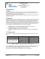
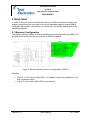
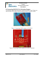
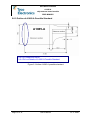
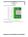
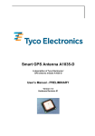
GPS Smart Antenna A1085-A
A description of Tyco Electronics’
GPS antenna modules
User’s Manual - PRELIMINARY
Version 1.4
Hardware Revision 01
This page was intentionally left blank.
Revision History
Revision History
Rev.
1.0
1.1
1.2
1.3
Date
11-10-06
02-09-07
02-15-07
02-16-07
1.4
06-18-07
mm-dd-yy
V1.4 - 06/07
Description
Initial Draft.
Review and release
Reworked
New project name A1035-CA, clear differentiation between
samples and final product
Final product name: A1085-A
User’s Manual
Page 3 of 19
Disclaimer
Disclaimer
THIS DOCUMENT CONTAINS PROPRIETARY INFORMATION OF TYCO ELECTRONICS CORPORATION/POWER SYSTEMS (TYCO ELECTRONICS). IT MAY
NOT BE COPIED OR TRANSMITTED BY ANY MEANS, PASSED TO OTHERS,
OR STORED IN ANY RETRIEVAL SYSTEM OR MEDIA, WITHOUT PRIOR
CONSENT OF TYCO ELECTRONICS OR ITS AUTHORIZED AGENTS.
THE INFORMATION IN THIS DOCUMENT IS, TO THE BEST OF OUR
KNOWLEDGE, ENTIRELY CORRECT. HOWEVER, TYCO ELECTRONICS CAN
NEITHER ACCEPT LIABILITY FOR ANY INACCURACIES, OR THE
CONSEQUENCES THEREOF, NOR FOR ANY LIABILITY ARISING FROM THE
USE OR APPLICATION OF ANY CIRCUIT, PRODUCT, OR EXAMPLE SHOWN IN
THE DOCUMENT.
THE PRODUCT (HARD- AND SOFTWARE) DESCRIBED IN THIS DOCUMENTATION IS NOT AUTHORIZED FOR USE IN LIFE SUPPORT DEVICES OR
SYSTEMS WITHOUT THE EXPRESS WRITTEN APPROVAL OF TYCO ELECTRONICS.
THIS DOCUMENT MAY PROVIDE LINKS TO OTHER WORLD WIDE WEB SITES
OR RESOURCES. BECAUSE TYCO ELECTRONICS HAS NO CONTROL OVER
SUCH SITES AND RESOURCES, TYCO ELECTRONICS SHALL NOT BE
RESPONSIBLE FOR THE AVAILABILITY OF SUCH EXTERNAL SITES OR
RESOURCES, AND DOES NOT ENDORSE AND IS NOT RESPONSIBLE OR
LIABLE FOR ANY CONTENT, ADVERTISING, PRODUCTS, OR OTHER
MATERIALS ON OR AVAILABLE FROM SUCH SITES OR RESOURCES. TYCO
ELECTRONICS SHALL NOT BE RESPONSIBLE OR LIABLE, DIRECTLY OR
INDIRECTLY, FOR ANY DAMAGE OR LOSS CAUSED OR ALLEGED TO BE
CAUSED BY OR IN CONNECTION WITH USE OF OR RELIANCE ON ANY SUCH
CONTENT, GOODS OR SERVICES AVAILABLE ON OR THROUGH ANY SUCH
SITE OR RESOURCE.
TYCO ELECTRONICS RESERVES THE RIGHT TO CHANGE, MODIFY, OR
IMPROVE THIS DOCUMENT OR THE PRODUCT DESCRIBED HEREIN, AS
SEEN FIT BY TYCO ELECTRONICS WITHOUT FURTHER NOTICE.
Page 4 of 19
User’s Manual
V1.4 - 06/07
Table of Contents
Table of Contents
1 Introduction ........................................................................................................ 6
1.1 Note .................................................................................................................. 6
1.2 Overview ........................................................................................................... 6
1.3 Characteristics .................................................................................................. 6
1.4 Handling Precautions ........................................................................................ 7
2 Quick Start.......................................................................................................... 8
2.1 Minimum Configuration ..................................................................................... 8
2.2 Important Information on Samples .................................................................... 9
2.3 Serial Port Settings ........................................................................................... 9
2.4 Improved TTFF ................................................................................................. 9
2.5 Connecting EVA1035-C for Evaluation Purpose ............................................. 10
2.6 Mechanical Outline.......................................................................................... 11
2.6.1 Outline of A1085-A Sample ...................................................................................... 11
2.6.2 Outline of A1085-A Possible Standard ..................................................................... 12
2.6.3 Pin-out Details of A1085-A Samples ........................................................................ 13
2.6.4 Pin-out Details of A1085-A Possible Standard ......................................................... 14
2.7 Description A1085-A Signals .......................................................................... 15
2.7.1 Pin-out ...................................................................................................................... 15
2.7.2 Absolute Maximum Ratings...................................................................................... 15
2.8 Recommended Profile for Reflow Soldering ................................................... 16
3 Quality and Reliability...................................................................................... 17
3.1 Environmental Conditions ............................................................................... 17
3.2 Product Qualification ....................................................................................... 17
3.3 Production Test ............................................................................................... 17
4 Related Information ......................................................................................... 18
4.1 Contact............................................................................................................ 18
4.2 Related Documents......................................................................................... 18
5 List of Tables .................................................................................................... 19
6 List of Figures .................................................................................................. 19
V1.4 - 06/07
User’s Manual
Page 5 of 19
GPS Smart Antenna
A1085-A
chip antenna based module
PRELIMINARY
1 Introduction
1.1 Note
Please note that this is a preliminary revision of the User’s Manual. The final version might differ form the herein described contents. The name A1085-A is to be
considered the project name for this product.
This document explains handling of special samples provided. Please consider all
remarks carefully!
1.2 Overview
Tyco Electronics’ A1085-A chip antenna module is a highly integrated GPS receiver
(A1080-A) combined with a small and high performance chip antenna and can be
used as an SMD component. It is capable to receive signals from up to 20 GPS
satellites and transferring them into position and timing information that can be read
over a serial port. This new generation of GPS antenna modules combines small
size and high-end GPS functionality at low power consumption:
•
•
•
•
Operable at 3.3V / 90mW during tracking mode @ 1fix per second
Small form factor of 33 x 16,7 mm (1.30” x 0.66”)
Small high performance chip antenna onboard
Single-sided SMD component, for reflow soldering (only mass production
units)
1.3 Characteristics
The modules are characterized by the following parameters (under full sky conditions).
Channels
Frequency
Position Accuracy
Time To First Fix – TTFF
(theoretical minimum values;
values in real world may differ)
Stand alone
Obscuration recovery (1)
Hot start (2)
Warm (3)
Cold (4)
20, parallel tracking
L1 (= 1575 MHz)
5m CEP (SA off)
1s
2s typical
32s typical
35s typical
Table 1: A1085-A chip antenna module characteristics
(1)
(2)
(3)
(4)
The calibrated clock of the receiver has not stopped, thus it knows precise time (to the µs level).
The receiver has estimates of time/date/position and valid almanac and ephemeris data.
The receiver has estimates of time/date/position and recent almanac.
The receiver has no estimate of time/date/position, and no recent almanac.
Page 6 of 19
User’s Manual
V1.4 - 06/07
GPS Smart Antenna
A1085-A
chip antenna based module
PRELIMINARY
Mechanical dimensions
Length
Width
Height
Weight
33mm, 1.30”
16.7mm, 0.66”
3.0mm, 0.12”
2g, < 0.10oz
Table 2: A1085-A chip antenna module dimensions and weight
1.4 Handling Precautions
The GPS antenna modules A1085-A are sensitive to electrostatic discharge (ESD).
Please handle with appropriate care.
V1.4 - 06/07
User’s Manual
Page 7 of 19
GPS Smart Antenna
A1085-A
chip antenna based module
PRELIMINARY
2 Quick Start
In order to allow an easy and quick start with the A1085-A antenna modules, this
chapter provides a short overview on the most important steps to receive NMEA
messages with position information on a serial port. For details please refer to the
according chapters.
2.1 Minimum Configuration
The following picture shows a recommended minimum configuration for NMEA output and commands received and sent via an RS232 interface.
Figure 1: Recommended minimum configuration A1085-A
Remarks:
•
•
Place C1 to C5 close to MAX3232. For capacity values see datasheet of actual component used.
Use 3.3V level shifter (MAX3232 or equivalent).
Page 8 of 19
User’s Manual
V1.4 - 06/07
GPS Smart Antenna
A1085-A
chip antenna based module
PRELIMINARY
2.2 Important Information on Samples
(1) Please make sure that the samples of A1085-A are covered to reduce the influence of temperature fluctuations.
(2) Samples of A1085-A chip antenna modules are using antistatic foam material to
reduce temperature fluctuations.
(3) The antennas of these samples are adjusted and optimized for best GPS performance without any enclosure or housing, for free air condition.
Figure 2: Foam protected chip antenna sample
2.3 Serial Port Settings
The default configuration within the standard GPS firmware is:
•
Serial 0 (TXA/RXA - NMEA) 4800 baud, 8 data bits, no parity, 1 stop bit, no
flow control
2.4 Improved TTFF
In order to improve the TTFF (Time To First Fix), it is recommended to support the
RTC with a back-up battery when no system power is available.
If the GPS smart antenna should not be backed-up it is possible to support the restart procedure by providing position and date/time information to the module. This
is described in the firmware manual. Please refer there to chapter Start-up Support
in the document T.E. GPS Firmware A1080.
V1.4 - 06/07
User’s Manual
Page 9 of 19
GPS Smart Antenna
A1085-A
chip antenna based module
PRELIMINARY
2.5 Connecting EVA1035-C for Evaluation Purpose
For evaluation purpose we recommend to use the EVA1035-C board. Please connect the cable of the A1085-A antenna module as shown in the picture below.
Figure 3: Connecting A1085-A sample to EVA1035-C
Figure 4: Connecting A1085-A sample to EVA1035-C (detailed)
Page 10 of 19
User’s Manual
V1.4 - 06/07
GPS Smart Antenna
A1085-A
chip antenna based module
PRELIMINARY
2.6 Mechanical Outline
All dimensions in this chapter are given in mm and (inch), respectively. Tolerances
are according to PCB manufacturing accuracy and usually in the range of ± 0.2mm.
2.6.1 Outline of A1085-A Sample
Pin Out: please see below
2.6.3 Pin-out Details of A1085-A Samples
Figure 5: Outline A1085-A sample
V1.4 - 06/07
User’s Manual
Page 11 of 19
GPS Smart Antenna
A1085-A
chip antenna based module
PRELIMINARY
2.6.2 Outline of A1085-A Possible Standard
A1085-A
Pin Out: please see below
2.6.4 Pin-out Details of A1085-A Possible Standard
Figure 5: Outline A1085-A possible standard
Page 12 of 19
User’s Manual
V1.4 - 06/07
GPS Smart Antenna
A1085-A
chip antenna based module
PRELIMINARY
2.6.3 Pin-out Details of A1085-A Samples
All dimensions in [mm, (inch)]
Figure 6: Pin-out details of A1085-A sample
The pin coordinates shown in the figure are center positions. Pin dimensions are
0.8 mm (width) by 1.1 mm (depth).
V1.4 - 06/07
User’s Manual
Page 13 of 19
GPS Smart Antenna
A1085-A
chip antenna based module
PRELIMINARY
2.6.4 Pin-out Details of A1085-A Possible Standard
All dimensions in [mm, (inch)]
Figure 6: Pin-out details of A1085-A possible standard
Note: Additional GND solder pads will be added to each side of the module. The
two shown solder pads are examples. The final position depends on electrical constraints and mechanical demands!
The pin coordinates shown in the figure are center positions. Pin dimensions are
0.8 mm (width) by 1.1 mm (depth).
Page 14 of 19
User’s Manual
V1.4 - 06/07
GPS Smart Antenna
A1085-A
chip antenna based module
PRELIMINARY
2.7 Description A1085-A Signals
These tables describe the functionality of the pins and their associated symbols.
2.7.1 Pin-out
Pin
1
2
3
4
5
6
7
8
9
10
11
Name
GND
VCC
Vbak
1PPS
RXB
TXB
TXA
RXA
nRST
NC
Boot
Function
Ground
3.3 – 3.6 VDC
Backup supply
1 pulse per second timing signal
second serial port, receive
second serial port, transmit
first serial port, transmit
first serial port, receive
Reset
Not connected
Boot select
Comment
Power supply
Unused by default
Unused by default
NMEA out
NMEA in
Do not connect
Leave open for normal operation
Table 3: Pin out description
2.7.2 Absolute Maximum Ratings
Symbol
Vcc
Vin
Iov
Itdv
Tst
Parameter
Power supply
Voltage to any pin
Input current on any pin
Absolute sum of all input currents during overload
condition
Storage temperature
Min
-0.3
-0.3
-10
Max
+3.6
+3.6
10
200
Unit
V
V
mA
mA
-55
125 °C
Table 4: Absolute maximum ratings
Stresses beyond those listed under “Absolute Maximum Ratings” may cause permanent damage to the device. This is a stress rating only. Functional operation of
the device at these or any other conditions beyond those indicated in the operational sections of this specification is not implied. Exposure to absolute maximum
rating conditions for extended periods may affect device reliability.
V1.4 - 06/07
User’s Manual
Page 15 of 19
GPS Smart Antenna
A1085-A
chip antenna based module
PRELIMINARY
2.8 Recommended Profile for Reflow Soldering
Typical values for reflow soldering of the module in convection or IR/convection ovens are as follows:
Peak temperature
Average ramp up rate to Peak (183°C to Peak)
Preheat temperature 125 (±25°C)
Temperature maintained above 183°C
Time within 5°C of actual peak temperature
Ramp Down rate
Time 25°C to peak temperature
235°C
3°C / second max.
120 seconds max.
60 … 150 seconds
10 … 20 seconds
6°C / second max.
6 minutes max.
Table 5: Reflow soldering profile A1085-A
As results of soldering may vary among different soldering systems and types of
solder and depend on additional factors like density and types of components on
board, the values above should be considered as a starting point for further optimization.
Page 16 of 19
User’s Manual
V1.4 - 06/07
GPS Smart Antenna
A1085-A
chip antenna based module
PRELIMINARY
3 Quality and Reliability
3.1 Environmental Conditions
Operating temperature
Operating humidity
MSL JEDEC
(Moisture Sensitivity Level)
Storage
- 30 … + 70°C
Max. 85% r. H., non-condensing, at 85°C
3
6 months in original package.
Table 6: Environmental conditions
3.2 Product Qualification
Prior to product qualification the GPS receiver is preconditioned according to
EIA/JEDEC standard JESD22-A113-B / Level 3.
Basic qualification tests:
•
•
•
•
•
•
•
Reflow simulation on test PCB
Temperature Cycling –30°C … +70°C
Temperature Humidity Bias 70°C / 85% RH
High / Low Temperature Operating –30° / +70°C
High Temperature Operating Life +70°C
Vibration Variable Frequency
Mechanical Shock
Please contact Tyco Electronics for detailed information.
3.3 Production Test
Each module is electrically tested prior to packing and shipping to ensure state of
the art GPS receiver performance and accuracy.
V1.4 - 06/07
User’s Manual
Page 17 of 19
GPS Smart Antenna
A1085-A
chip antenna based module
PRELIMINARY
4 Related Information
4.1 Contact
This manual was created with due diligence. We hope that it will be helpful to the
user to get the most out of the GPS module.
Anyway, inputs about errors or mistakable verbalizations and comments or proposals to TYCO Electronics, Power Systems in Munich, Germany, for further improvements are highly appreciated.
Product Marketing Manager
Positioning Products
Tel.: +49 89 6089 837
Fax: +49 89 6089 835
Tyco Electronics Corporation
Power Systems
Finsinger Feld 1
85521 Ottobrunn, Germany
Email to [email protected].
Please visit our website at www.tycoelectronics.com/gps.
4.2 Related Documents
• Manual: T.E. GPS Firmware A1080-A (TYCO)
• Manual: T.E. GPS Evaluation Kit DKS1035 (TYCO)
Page 18 of 19
User’s Manual
V1.4 - 06/07
Lists of Tables
and Figures
5 List of Tables
Table 1: A1085-A chip antenna module characteristics ........................................... 6
Table 2: A1085-A chip antenna module dimensions and weight.............................. 7
Table 3: Pin out description.................................................................................... 15
Table 4: Absolute maximum ratings ....................................................................... 15
Table 5: Reflow soldering profile A1085-A ............................................................. 16
Table 6: Environmental conditions ......................................................................... 17
6 List of Figures
Figure 1: Recommended minimum configuration A1085-A...................................... 8
Figure 2: Foam protected chip antenna sample....................................................... 9
Figure 3: Connecting A1085-A sample to EVA1035-C........................................... 10
Figure 4: Connecting A1085-A sample to EVA1035-C (detailed)........................... 10
Figure 5: Outline A1085-A sample ......................................................................... 11
Figure 5: Outline A1085-A possible standard......................................................... 12
Figure 6: Pin-out details of A1085-A sample.......................................................... 13
Figure 6: Pin-out details of A1085-A possible standard ......................................... 14
V1.4 - 06/07
User’s Manual
Page 19 of 19