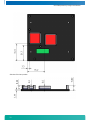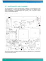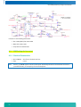
1
microETXexpress®-PC Document Revision 0.1 If it’s embedded, it’s Kontron. » Table of Contents « 1 User Information ............................................................................. 1 1.1 About This Document ................................................................................................................. 1 1.2 Copyright Notice ....................................................................................................................... 1 1.3 Trademarks .............................................................................................................................. 1 1.4 Standards ................................................................................................................................ 1 1.5 Warranty ................................................................................................................................. 2 1.6 Technical Support ..................................................................................................................... 2 2 Introduction ................................................................................... 3 2.1 microETXexpress®-PC ................................................................................................................ 3 2.2 Naming clarification .................................................................................................................. 3 2.3 Understanding microETXexpress®-PC functionality.......................................................................... 4 2.4 COMexpress™ Documentation ...................................................................................................... 4 2.5 COMexpress™ Benefits ............................................................................................................... 4 3 Specification .................................................................................. 6 3.1 Functional Specification ............................................................................................................. 6 3.2 Available modules ..................................................................................................................... 7 3.3 Block Diagram .......................................................................................................................... 8 3.4 Meachnical Specification ............................................................................................................ 9 3.5 Electical Specification ................................................................................................................ 9 3.5.1 Supply Voltage ........................................................................................................................ 9 3.5.2 Supply Voltage Ripple ............................................................................................................... 9 3.5.3 Supply Current 5V_STB.............................................................................................................. 9 3.5.4 Supply Current (Windows XP SP3) ................................................................................................ 9 3.5.5 CMOS Battery Power Consumption ............................................................................................. 10 3.6 Environmental Specification ..................................................................................................... 10 3.7 MTBF .................................................................................................................................... 10 4 microETXexpress®-PC Connectors ..................................................... 12 www.kontron.com 4.1 Connector Locations ................................................................................................................ 12 4.2 Pinout List ............................................................................................................................. 13 4.2.1 General Signal Description....................................................................................................... 13 4.2.2 Connector X1A (A1 - A55) ........................................................................................................ 14 4.2.3 Connector X1A (A56-A110) ...................................................................................................... 15 4.2.4 Connector X1A (B1 - B55) ........................................................................................................ 16 4.2.5 Connector X1B (C1 - C55) ........................................................................................................ 17 4.2.6 Connector X1B (C56 - C110) ..................................................................................................... 18 4.2.7 Connector X1B (D1 - D55) ........................................................................................................ 19 4.2.8 Connector X1B (D56 - D110) .................................................................................................... 20 4.2.9 Alternative Pinout of HDMI ...................................................................................................... 21 4.2.10 Alternative Pinout of Display Port.............................................................................................. 21 4.3 Signal Description ................................................................................................................... 22 4.3.1 PCIexpress x1 lanes ................................................................................................................ 22 4.3.2 USB..................................................................................................................................... 22 4.3.3 SATA ................................................................................................................................... 22 4.3.4 Audio .................................................................................................................................. 23 4.3.5 Serial IRQ ............................................................................................................................. 23 4.3.6 VGA Output ........................................................................................................................... 23 4.3.7 LVDS Flat Panel Interface (JILI) ................................................................................................ 23 4.3.8 PCIexpress Graphics ............................................................................................................... 23 4.3.9 SDVO ................................................................................................................................... 24 4.3.10 HDMI ................................................................................................................................... 24 4.3.11 Displayport ........................................................................................................................... 24 4.3.12 Ethernet .............................................................................................................................. 24 4.3.13 Power Control ....................................................................................................................... 24 4.3.14 Power Management ................................................................................................................ 25 4.3.15 Miscellaneous Circuits............................................................................................................. 25 4.3.16 I2C Bus ................................................................................................................................ 25 5 Special Features ............................................................................ 27 5.1 Watchdog Timer ...................................................................................................................... 27 5.2 GPIO - General Purpose Input and Output..................................................................................... 28 5.3 Usage of Different Graphic interfaces .......................................................................................... 29 5.4 Available Graphic interfaces ...................................................................................................... 29 6 Design Consideration...................................................................... 31 www.kontron.com 6.1 Thermal Management .............................................................................................................. 31 6.2 Heatspreader Dimension .......................................................................................................... 32 6.3 microETXexpress®-PC onboard fan connector ............................................................................... 34 6.3.1 Location and pinout of fan connector ........................................................................................ 34 6.3.2 BIOS Settings for fan control .................................................................................................... 35 6.3.3 Electrical Characteristics ......................................................................................................... 35 7 System Ressources ......................................................................... 36 8 BIOS Operation ............................................................................. 37 8.1 Determining the BIOS Version ................................................................................................... 37 8.2 Setup Guide ........................................................................................................................... 37 8.2.1 Start AMI® BIOS Setup Utility .................................................................................................. 37 8.3 BIOS Setup ............................................................................................................................ 39 9 Appendix A: JIDA Standard .............................................................. 40 9.1 JIDA Information .................................................................................................................... 40 10 Appendix B: Architecture Information ................................................ 41 10.1 Buses.................................................................................................................................... 41 10.1.1 ISA, Standard PS/2 – Connectors .............................................................................................. 41 10.1.2 PCI/104 ............................................................................................................................... 41 10.2 General PC Architecture ............................................................................................................ 41 10.3 Ports .................................................................................................................................... 42 10.3.1 RS-232 Serial ........................................................................................................................ 42 10.3.2 Serial ATA ............................................................................................................................. 42 10.3.3 USB..................................................................................................................................... 42 10.4 Programming ......................................................................................................................... 42 11 Appendix C: Document Revision History.............................................. 43 www.kontron.com microETXexpress®-PC / User Information 1 User Information 1.1 About This Document This document provides information about products from Kontron Embedded Modules GmbH and/or its subsidiaries. No warranty of suitability, purpose, or fitness is implied. While every attempt has been made to ensure that the information in this document is accurate, the information contained within is supplied “as-is” and is subject to change without notice. For the circuits, descriptions and tables indicated, Kontron assumes no responsibility as far as patents or other rights of third parties are concerned. 1.2 Copyright Notice Copyright © 2003-2009 Kontron Embedded Modules GmbH All rights reserved. No part of this document may be reproduced, transmitted, transcribed, stored in a retrieval system, or translated into any language or computer language, in any form or by any means (electronic, mechanical, photocopying, recording, or otherwise), without the express written permission of Kontron Embedded Modules GmbH. DIMM-PC®, PISA®, ETX®, ETXexpress®, microETXexpress™, X-board®, DIMM-IO® and DIMM-BUS® are trademarks or registered trademarks of Kontron Embedded Modules GmbH. Kontron is trademark or registered trademark of Kontron AG. 1.3 Trademarks The following lists the trademarks of components used in this board. » IBM, XT, AT, PS/2 and Personal System/2 are trademarks of International Business Machines Corp. » Microsoft is a registered trademark of Microsoft Corp. » Intel is a registered trademark of Intel Corp. » All other products and trademarks mentioned in this manual are trademarks of their respective owners. 1.4 Standards Kontron Embedded Modules GmbH is certified to ISO 9000 standards. 1 microETXexpress®-PC / User Information 1.5 Warranty This Kontron Embedded Modules GmbH product is warranted against defects in material and workmanship for the warranty period from the date of shipment. During the warranty period, Kontron Embedded Modules GmbH will at its discretion decide to repair or replace defective products. Within the warranty period, the repair of products is free of charge as long as warranty conditions are observed. The warranty does not apply to defects resulting from improper or inadequate maintenance or handling by the buyer, unauthorized modification or misuse, operation outside of the product’s environmental specifications or improper installation or maintenance. Kontron Embedded Modules GmbH will not be responsible for any defects or damages to other products not supplied by Kontron Embedded Modules GmbH that are caused by a faulty Kontron Embedded Modules GmbH product. 1.6 Technical Support Technicians and engineers from Kontron Embedded Modules GmbH and/or its subsidiaries are available for technical support. We are committed to making our product easy to use and will help you use our products in your systems. Please consult our Web site at http://www.kontron.com/support for the latest product documentation, utilities, drivers and support contacts. Consult our customer section http://emdcustomersection.kontron.com for the latest BIOS downloads, Product Change Notifications and additional tools and software. In any case you can always contact your board supplier for technical support. 2 microETXexpress®-PC / Introduction 2 Introduction 2.1 microETXexpress®-PC Based on the COM Express standard, Kontron’s microETXexpress®-PC, powered by a variety of Intel®'s Core2Duo® and CeleronM® processors, is a next-generation embedded module that brings advanced technology to tomorrow’s applications, as well as continuing today’s legacy devices. Built around serial differential signaling technologies, microETXexpress®-PC modules incorporate the following interfaces into 95 x 125 small form factor embedded module: » PCI Express, which provides a high performance I/O infrastructure with transfer rates starting at 2.5 Giga transfers per second over a x1 PCI Express lane » PCI » Serial ATA (SATA II) » USB 2.0 » LVDS » Azalia High Definition Audio » Advanced Configuration and Power Interface (ACPI) for optimized power management The microETXexpress®-PC is built around the Intel® Core2Duo® and CeleronM® processor and the Intel® GS45 chipset. These modules feature the most current desktop features such as USB 2.0, SATA, and PCI Express buses. The microETXexpress®-PC delivers up to 4GB DDR3 RAM. For applications that require advanced real-time video capabilities, the microETXexpress®-PC has integrated graphics with 2D, 3D and Motion Video Acceleration and also supports PCI Express graphics, two SDVO ports or two HDMI capable DVI ports. Fast communications are possible courtesy of a Gigabit Ethernet port. The microETXexpress®-PC supports up to 6 PCI Express x1 Lanes and PCI Express cards (only when 10/100MB Ethernet is equipped) as well as established hardware solutions based on current buses such as 32-bit PCI. A Gigabit Ethernet port provides fast connectivity to LAN/WAN and 8 USB 2.0 ports provide fast and sufficient interfaces for external peripherals. microETXexpress®-PC modules also provide the following interfaces that are always located in the same physical position on each board: PCI-express, PCI32, USB, serial ATA (SATA), parallel ATA (PATA), LVDS Multi Media ports, as well as an ACPI (Advanced Configuration and Power Interface) for optimized power management. Mounting holes on the board provide secure mounting to allow the module increased shock and vibration resistance. 2.2 Naming clarification COMexpress™ defines a Computer-On-Module, or COM, with all components necessary for a bootable host computer, packaged as a super component. Interfaces will provide a smooth transition path from legacy parallel interfaces to LVDS (Low Voltage Differential Signaling) interfaces. These include the PCI bus and parallel ATA and PCI Express and Serial ATA. 3 microETXexpress®-PC / Introduction » ETXexpress® modules are Kontron's COMexpress™ modules in basic form factor (125mm x 95mm) » microETXexpress® modules are Kontron's COMexpress™ modules in compact form factor (95mm x 95mm) » nanoETXexpress® modules are Kontron's COMexpress™ modules in the future ultra form factor (55mm x 84mm) 2.3 Understanding microETXexpress®-PC functionality All Kontron ETXexpress® and microETXexpress® modules contain two connectors; each of it has two rows. The primary connector has two rows called Row A and Row B. The secondary connector has two rows called Row C and Row D. The primary connector (Row A and Row B) feature the following legacy-free functionality: » Ethernet » Serial ATA (SATA) » USB 2.0 » LVDS/VGA and dual display video » Intel High Definition Audio (Azalia) » LPC (low pin count) Bus The secondary connector (Row C and Row D) provides support for the following buses and I/O: » PCI Express » PCI » IDE 2.4 COMexpress™ Documentation This product manual serves as one of three principal references for a COMexpress™ design. It documents the specifications and features of microETXexpress®-DC. The other two references, which are available from your Kontron Support or from PICMG®, include: » The COMexpress Specification defines the COMexpress™ module form factor, pinout, and signals. This document ist available from the PIGMG website by filling out the order form. » The COMExpress™ Design Guide by PICMG serves as a general guide for baseboard design, with a focus on maximum flexibility to accommodate a wide range of COMexpress™ modules. Note: Some of the information contained within this product manual applies only to certain product revisions (CE: xxx). If certain information applies to specific product revisions (CE: xxx) it will be stated. Please check the product revision of your module to see if this information is applicable. 2.5 COMexpress™ Benefits Computer on modules express (COMexpress) modules in compact formfactor are very compact (95 x 95 mm, 12mm thick), highly integrated computers. All (micro)ETXexpress® modules feature a standardized form factor and a standardized connector layout that carry a specified set of signals. Each microETXexpress® module is based on 4 microETXexpress®-PC / Introduction connector type 2 of the COMexpress specification. This standardization allows designers to create a single-system baseboard that can accept present and future (micro)ETXexpress® modules. microETXexpress® modules include common personal computer (PC) peripheral functions such as: » Graphics » USB ports » Ethernet » Sound » IDE (and SATA) The baseboard designer can optimize exactly how each of these functions implements physically. Designers can place connectors precisely where needed for the application on a baseboard designed to optimally fit a system’s packaging. A peripheral PCI bus can be implemented directly on the baseboard rather than on mechanically unwieldy expansion cards. The ability to build a system on a single baseboard using the computer as one plug-in component simplifies packaging, eliminates cabling, and significantly reduces system-level cost. A single baseboard design can use a range of ETXexpress®, microETXexpress® and nanoETXexpress modules. This flexibility can differentiate products at various price/performance points, or to design future proof systems that have a built-in upgrade path. The modularity of a COMexpress™ solution also ensures against obsolescence as computer technology evolves. A properly designed COMexpress™ baseboard can work with several successive generations of COMexpress® modules. A COMexpress™ baseboard design has many advantages of a custom, computer-board design but delivers better obsolescence protection, greatly reduced engineering effort, and faster time to market. 5 microETXexpress®-PC / Specification 3 Specification 3.1 Functional Specification Processor: Intel® Core2Duo (Penryn) » CPU: 45nm Penryn SL9400, SU9300 or CM722 » Cache: 3MB (CM722) or 6MB Chipset Northbridge:Intel® GS45 » Speed: 667 / 800 / 1066 MHz FSB » RAM: single channel up 4GB DDR3-667/800/1066 on SODIMM socket » PEG: One x16 PCIe port for PCI Express based graphic cards Chipset Southbridge: Intel® ICH-9M » USB: 8 x USB 1.1/2.0 » Audio: Intel® High Definition Audio (24 bit / 96 kHz) » PCI Express: 5 x PCI Express x1 (x4 possible) » PCI bus: 32bit / 33MHz Integrated graphics: Intel® GMAX4500 » Graphics Memory: up to 1024 MByte » Features: HDTV/HD capable, Decoder for MPEG2(HD) / H.264, DirectX®10.0, OpenGL 2.0, Pixelshader 4.0 Display Interfaces » CRT: maximum resolution up to QXGA (2048x1536) » Flat Panel: dual channel 18bit and 24bit (with dithering) up to UXGA (1600x1200) » Digital Display: 2 SDVO channels (muxed with PEG) supporting external SDVO components (HDMI, DVI, LVDS, TV-out) » HDMI » DisplayPort 6 microETXexpress®-PC / Specification Storage » SATA: 3 SATA ports up to 300 MB/S supporting NCQ, Hotplug, Staggered Spinup, eSATA, PortMultiplier, RAID 0, RAID1, Matrix-RAID » IDE: One Channel over JMD330 SATA2PATA Bridge Onboard Devices: » Ethernet: Intel® 82567 10/100/1000 Phy » TPM: TPM 1.2, integrated in Southbridge » Watchdog: onboard CPLD with integrated Watchdog functionality Additional Interfaces: » LPC: Yes » SMBus: Yes » I2C: Yes » GPIO: 8, Fixed to 4 GPI or 4 GPO via JIDA interface Power Management & Misc » JIDA support: Yes » MARS support: Yes » HWM: Temperature Monitoring for CPU and Board Temperature » Passice Cooling: Passice and Critical Trip Point (with BIOS NOW1R112 or newer) » ACPI: ACPI 1.0 / 2.0 / 3.0 » S-States: S0, S3, S4, S5 » Input Voltage: Single supply support with wide range input 8.5 V - 18 V 3.2 Available modules Part No 36004-0000-19-2 Intel® CPU SL9400 36004-0000-12-2 SU9300 36004-0000-12-1 722 7 microETXexpress®-PC / Specification 3.3 8 Block Diagram microETXexpress®-PC / Specification 3.4 Meachnical Specification Dimensions » 95.0 mm x 114.0 mm (3.75” x 4.5”) » Height approx. 12 mm (0.4”) 3.5 Electical Specification 3.5.1 Supply Voltage » VCC: 12V DC +/- 5% or » 8.5V DC to 18V DC wide range input » 5V_Stb: 5V DC +/- 5% but always equal or lower VCC Note: It is not possible to use E2 rated boards with wide range input! Note: It is recommended to follow the ATX specification for voltage rise times which claims: "The output voltage shall rise from ≤ 10% of nominal to within the regulation ranges … within 0.1ms to 20ms". 3.5.2 Supply Voltage Ripple » Maximum 100 mV peak to peak 0 – 20 MHz 3.5.3 Supply Current 5V_STB » Typical 50 mA, peak up to 350 mA (S3) 3.5.4 Supply Current (Windows XP SP3) The tested boards were mounted on a Kontron Evaluation Board (Article number: 38100-0000-00-0), a mouse and a keyboard were connected. The Power-consumption tests were executed during Windows XP SP2 by using a tool to stress the CPU (100 % load). The power measurements values were acquired after 15 min full load and a stable CPU die temperature. To ensure a stable die temperature a corresponding heatsink was used to hold the temperature under the critical trip point. All boards were equipped with TBD of memory. The Modules were tested using maximum CPU frequency. Mode [A] 5V [A] 5VSB [W] Full Load TBD TBD TBD Idle TBD TBD TBD Idle with C1E/EIST TBD TBD TBD 9 microETXexpress®-PC / Specification Standby S1 TBD TBD TBD Standby S3 TBD TBD TBD Soft Off S5 TBD TBD TBD 3.5.5 CMOS Battery Power Consumption CMOS battery power consumption was measured with a microETXexpress®-DC module on a standard Kontron ETX® evaluation board. The system was turned off and the battery was removed from the evaluation board. The 2.5 V or 3.0 V of power was supplied from a DC power supply. Do not use these values to calculate the CMOS battery lifetime. TBD 3.6 Environmental Specification Temperature Operating: (with Kontron Embedded Modules GmbH heat-spreader plate assembly): » Ambient temperature: 0 to +60 °C » Maximum heatspreader-plate temperature: 0 to +60 °C (*) » Non-operating: -30 to +85 °C Note: *The maximum operating temperature with the heatspreader plate is the maximum measurable temperature on any spot on the heatspreader’s surface. You must maintain the temperature according to the above specification. Operating (without Kontron Embedded Modules GmbH heat-spreader plate assembly): » Maximum operating temperature: 0 to +60 °C (**) » Non operating: -30 to +85 °C Note: **The maximum operating temperature is the maximum measurable temperature on any spot on a module’s surface. You must maintain the temperature according to the above specification. Humidity » Operating: 10% to 90% (non condensing) » Non operating: 5% to 95% (non condensing) 3.7 MTBF The following MTBF (Mean Time Between Failure) values were calculated using a combination of manufacturer’s test data, if the data was available, and a Bellcore calculation for the remaining parts. 10 microETXexpress®-PC / Specification The Bellcore calculation used is “Method 1 Case 1”. In that particular method the components are assumed to be operating at a 50 % stress level in a 40° C ambient environment and the system is assumed to have not been burned in. Manufacturer’s data has been used wherever possible. The manufacturer’s data, when used, is specified at 50° C, so in that sense the following results are slightly conservative. The MTBF values shown below are for a 40° C in an office or telecommunications environment. Higher temperatures and other environmental stresses (extreme altitude, vibration, salt water exposure, etc.) lower MTBF values. System MTBF (hours): TBD Notes: 11 Fans usually shipped with Kontron Embedded Modules GmbH products have 50,000-hour typical operating life. The above estimates assume no fan, but a passive heat sinking arrangement Estimated RTC battery life (as opposed to battery failures) is not accounted for in the above figures and need to be considered for separately. Battery life depends on both temperature and operating conditions. When the Kontron unit has external power; the only battery drain is from leakage paths. microETXexpress®-PC / microETXexpress®-PC Connectors 4 microETXexpress®-PC Connectors The pinouts for microETXexpress® Interface Connectors X1A and X1B are documented for convenient reference. Please see the COMexpress™ Specification and COMexpress™ Design Guide for detailed, design-level information. 4.1 12 Connector Locations microETXexpress®-PC / microETXexpress®-PC Connectors 4.2 Pinout List 4.2.1 General Signal Description Type Description I/O-3,3 I/O-5T I/O-5 I-3,3 I/OD I-5T OA OD O-1,8 O-3,3 O-5 DP-I/O DP-I DP-O PU PD PWR Bi-directional 3,3 V IO-Signal Bi-dir. 3,3V I/O (5V Tolerance) Bi-directional 5V I/O-Signal 3,3V Input Bi-directional Input/Output Open Drain 3,3V Input (5V Tolerance) Output Analog Output Open Drain 1,8V Output 3,3V Output 5V Output Differential Pair Input/Output Differential Pair Input Differential Pair Output Pull-Up Resistor Pull-Down Resistor Power Connection Notes: 13 To protect external power lines of peripheral devices, make sure that: the wires have the right diameter to withstand the maximum available current the enclosure of the peripheral device fulfils the fire-protection requirements of IEC/EN60950 microETXexpress®-PC / microETXexpress®-PC Connectors 4.2.2 Connector X1A (A1 - A55) Pin Signal Description Type Termination Comment A1 A2 A3 A4 A5 A6 A7 A8 A9 A10 A11 A12 A13 A14 A15 A16 A17 A18 A19 A20 A21 A22 A23 A24 A25 A26 A27 A28 A29 A30 A31 A32 A33 A34 A35 A36 A37 A38 A39 A40 A41 A42 A43 A44 A45 A46 A47 A48 A49 A50 A51 A52 A53 A54 A55 GND GBE0_MDI3GBE0_MDI3+ GBE0_LINK1 GBE0_LINK1 GBE0_MDI2GBE0_MDI2+ GBE0_LINK# GBE0_MDI1GBE0_MDI1+ GND GBE0_MDI0GBE0_MDI0+ GBE0_CTREF SUS_S3# SATA0_TX+ SATA0_TXSUS_S4# SATA0_RX+ SATA0_RXGND SATA2_TX+ SATA2_TXSUS_S5# SATA2_RX+ SATA2_RXBATLOW# ATA_ACT# AC_SYNC AC_RST# GND AC_BITCLK AC_SDOUT BIOS_DISABL THRMTRIP# USB6USB6+ USB_6_7_OC USB4USB4+ GND USB2USB2+ USB_2_3_OC USB0USB0+ VCC_RTC EXCD0_PERST EXCD0_CPPE# LPC_SERIRQ GND PCIE_TX5+ PCIE_TX5GPI0 PCIE_TX4+ Power Ground GBE0_MDI3_N | Ethernet Receive GBE0_MDI3_P | Ethernet Receive GBE0_LINK100# | Ethernet Speed GBE0_LINK1000# | Ethernet Speed GBE0_MDI2_N | Ethernet Receive GBE0_MDI2_P | Ethernet Receive GBE0_LINK# | LAN Link LED GBE0_MDI1_N | Ethernet Receive GBE0_MDI1_P | Ethernet Receive Power Ground GBE0_MDI0_N | Ethernet Transmit GBE0_MDI0_P | Ethernet Transmit GBE0_CTREF PM_SLP_S3_EXT# opt. SATA_TX0_P | SATA 0 Transmit opt. SATA_TX0_N | SATA 0 Transmit PM_SLP_S4_EXT# opt. SATA_RX0_P | SATA 0 Receive opt. SATA_RX0_N | SATA 0 Receive Power Ground SATA_TX2_P | SATA 2 Transmit Data SATA_TX2_N | SATA 2 Transmit Data PM_SLP_S#5 SATA_RX2_P | SATA 2 Receive Data SATA_RX2_N | SATA 2 Receive Data PM_BATLOW# | Battery Low ATA_LED# | SATA LED HDA_SYNC | HD Audio Sync HDA_RST# | HD Audio Reset Power Ground HDA_BITCLK | HD Audio Clock HDA_SDOUT | HD Audio Data BIOS_DISABLE# EXT_THRMTRIP# USB6_N | USB Data – Port6 USB6_P | USB Data + Port6 USB_67_OC# | USB OverCurrent USB4_N | USB Data - Port4 USB4_P | USB Data + Port4 Power Ground USB2_N | USB Data - Port2 USB2_P | USB Data + Port2 USB_23_OC# | USB OverCurrent USB0_N | USB Data - Port0 USB0_P | USB Data + Port0 V_BAT EXCD0_PERST#|Express card reset EXCD0_CPPE#| capable c. request LPC_SERIRQ | Serial Interrupt Power Ground opt. PCI Express lane 5 + Transmit opt. PCI Express lane 5 - Transmit EXT_GPI0 | General Purpose Input 0 PCI Express lane 4 + Transmit PWR DP-I DP-I O-3,3 O-3,3 DP-I DP-I OD DP-I DP-I PWR DP-O DP-O O-1,8 O-3,3 Nc Nc O-3,3 Nc Nc PWR DP-O DP-O O-3,3 DP-I DP-I I-3,3 O-3,3 O-3,3 O-3,3 PWR O-3,3 O-3,3 I-3,3 I/ODPDPI-3,3 DPDPPWR DPDPI-3,3 DPDPPWR O-3,3 I-3,3 IO-3,3 PWR Nc Nc I-3,3 DP-O PU 10k 3,3V PU 8k25 3,3V PU 10k 3,3V PU 10k 3,3V PU 10k 3,3V PU 10k 3,3V PU 10k 3,3V PU 10k 3,3V PU 10k 3,3V - is on a power rail controlled by Intels - just available if - just available if - just available if - just available if int. PU 15k in ICH9 only active if opt. for x4: PU 1k 3,3V(S0) int. PD 20k in ICH9 int. PD 20k in ICH9 active only in S3 int. PD 20k in ICH9– x4 => PU 1k int. PD 15k in ICH9 | 5V tolerant int. PD 15k in ICH9 | 5V tolerant int. PD 15k in ICH9 | 5V tolerant int. PD 15k in ICH9 | 5V tolerant int. PD 15k in ICH9 | 5V tolerant int. PD 15k in ICH9 | 5V tolerant int. PD 15k in ICH9 | 5V tolerant int. PD 15k in ICH9 | 5V tolerant just available if no GbEthernet PHY is just available if no GbEthernet PHY is - Note: 14 The termination resistors in this table are already mounted on the ETXexpress® board. Refer to the design guide for information about additional termination resistors. microETXexpress®-PC / microETXexpress®-PC Connectors 4.2.3 Connector X1A (A56-A110) Pin Signal Description Type Termination Comment A56 A57 A58 A59 A60 A61 A62 A63 A64 A65 A66 A67 A68 A69 A70 A71 A72 A73 A74 A75 A76 A77 A78 A79 A80 A81 A82 A83 A84 A85 A86 A87 A88 A89 A90 A91 A92 A93 A94 A95 A96 A97 A98 A99 A100 A101 A102 A103 A104 A105 A106 A107 A108 A109 A110 PCIE_TX4GND PCIE_TX3+ PCIE_TX3GND PCIE_TX2+ PCIE_TX2GPI1 PCIE_TX1+ PCIE_TX1GND GPI2 PCIE_TX0+ PCIE_TX0GND LVDS_A0+ LVDS_A0LVDS_A1+ LVDS_A1LVDS_A2+ LVDS_A2LVDS_VDD_EN LVDS_A3+ LVDS_A3GND LVDS_A_CK+ LVDS_A_CKLVDS_I2C_CK LVDS_I2C_DAT GPI3 KBD_RST# KBD_A20GATE PCIE0_CK_REF+ PCIE0_CK_REFGND RSVD RSVD GPO0 RSVD RSVD GND VCC_12V VCC_12V VCC_12V GND VCC_12V VCC_12V VCC_12V VCC_12V VCC_12V VCC_12V VCC_12V VCC_12V VCC_12V GND PCI Express lane 4 - Transmit Power Ground PCI Express lane 3 + Transmit PCI Express lane 3 - Transmit Power Ground PCI Express lane 2 + Transmit PCI Express lane 2 - Transmit EXT_GPI1 | General Purpose Input 1 PCI Express lane 1 + Transmit PCI Express lane 1 - Transmit Power Ground EXT_GPI2 | General Purpose Input 2 PCI Express lane 0 + Transmit PCI Express lane 0 - Transmit Power Ground LVDS_A_DATA0_P | LVDS Channel A LVDS_A_DATA0_N | LVDS Channel A LVDS_A_DATA1_P | LVDS Channel A LVDS_A_DATA1_N | LVDS Channel A LVDS_A_DATA2_P| LVDS Channel A LVDS_A_DATA2_N | LVDS Channel A LVDS_VDD_EN | LVDS Panel Power LVDS_A_DATA3_P | LVDS Channel A LVDS_A_DATA3_N | LVDS Channel A Power Ground LVDS_A_CLK_P | LVDS Channel A LVDS_A_CLK_N | LVDS Channel A LVDS_DDC_CLK | JILI I2C Clock LVDS_DDC_DATA | JILI I2C Data EXT_GPI3 | General Purpose Input 3 KBD_RST# | Keyboard Reset KBD_A20GATE CLK_PCIE_CON_P CLK_PCIE_CON_N Power Ground n.c. n.c. EXT_GPO0 | General Purpose Output 0 n.c. n.c. Power Ground 12V VCC 12V VCC 12V VCC Power Ground 12V VCC 12V VCC 12V VCC 12V VCC 12V VCC 12V VCC 12V VCC 12V VCC 12V VCC Power Ground DP-O PWR DP-O DP-O PWR DP-O DP-O I-3,3 DP-O DP-O PWR I-3,3 DP-O DP-O PWR DP-O DP-O DP-O DP-O DP-O DP-O O-3,3 DP-O DP-O PWR DP-O DP-O I/OI/OI-3,3 I-3,3 I-3,3 DP-O DP-O PWR Nc Nc O-3,3 Nc Nc PWR PWR PWR PWR PWR PWR PWR PWR PWR PWR PWR PWR PWR PWR PWR PU 10k 3,3V (S0) PU 10k 3,3V (S0) PD 100k PU 2k21 3,3V (s0) PU 2k21 3,3V (s0) PU 10k 3,3V (S0) PU 10k 3,3V (S0) PU 10k 3,3V (S0) PD 10k - - Note: 15 - The termination resistors in this table are already mounted on the ETXexpress® board. Refer to the design guide for information about additional termination resistors. microETXexpress®-PC / microETXexpress®-PC Connectors 4.2.4 Connector X1A (B1 - B55) Pin Signal Description Type Termination Comment B1 B2 B3 B4 B5 B6 B7 B8 B9 B10 B11 B12 B13 B14 B15 B16 B17 B18 B19 B20 B21 B22 B23 B24 B25 B26 B27 B28 B29 B30 B31 B32 B33 B34 B35 B36 B37 B38 B39 B40 B41 B42 B43 B44 B45 B46 B47 B48 B49 B50 B51 B52 B53 B54 B55 GND GBE0_ACT LPC_FRAME# LPC_AD0 LPC_AD1 LPC_AD2 LPC_AD3 LPC_DRQ0# LPC_DRQ1# LPC_CLK GND PWRBTN# SMB_CK SMB_DAT SMB_ALERT# SATA1_TX+ SATA1_TXSUS_STAT# SATA1_RX+ SATA1_RXGND SATA3_TX+ SATA3_TXPWR_OK SATA3_RX+ SATA3_RXWDT AC_SDIN2 AC_SDIN1 AC_SDIN0 GND SPKR I2C_CK I2C_DAT THRM# USB7USB7+ USB_4_5_OC# USB5USB5+ GND USB3USB3+ USB_0_1_OC# USB1USB1+ EXCD1_PERST# EXCD1_CPPE# SYS_RESET# CB_RESET# GND PCIE_RX5+ PCIE_RX5GPO1 PCIE_RX4+ Power Ground GBE0_ACT# | Ethernet Activity LED LPC_FRAME# | LPC Frame Indicator LPC_AD0 | LPC Adress & DATA Bus LPC_AD1 | LPC Adress & DATA Bus LPC_AD2 | LPC Adress & DATA Bus LPC_AD3 | LPC Adress & DATA Bus LPC_DRQ#0 | LPC Request 0 LPC_DRQ#1 | LPC Request 1 CLK_LPC_33M_EXT |33MHz LPC clock Power Ground EXT_PWRBTN# | Power Button SMB_CLK_EXT | SMBUS Clock SMB_DATA_EXT | SMBUS Data SMB_ALERT# | SMBUS Interrupt SATA_TX1_P | SATA 1 Transmit Data + SATA_TX1_N | SATA 1 Transmit Data PM_SUS_ STAT# SATA_RX1_P | SATA 1 Receive Data + SATA_RX1_N | SATA 1 Receive Data Power Ground SATA_TX3_P | SATA 3 Transmit Data + SATA_TX3_N | SATA 3 Transmit Data EXT_PWR_OK | Power OK SATA_RX3_P | SATA 3 Receive Data + SATA_RX3_N | SATA 3 Receive Data WDT | Watch Dog Timer HDA_SDIN2_ICH| HD Audio Serial HDA_SDIN1_ICH| HD Audio Serial HDA_SDIN0_ICH| HD Audio Serial Power Ground HDA_SPKR | Speaker I2C_CLK_EXT | I2C clock I2C_DATA_EXT | I2C data PM_THRM# | Over Temperature USB7_N | USB Data – Port7 USB7_P | USB Data + Port7 USB_45_OC# | USB OverCurrent Port USB5_N | USB Data – Port5 USB5_P | USB Data + Port5 Power Ground USB3_N | USB Data – Port3 USB3_P | USB Data + Port3 USB_01_OC# | USB OverCurrent Port USB1_N | USB Data – Port1 USB1_P | USB Data + Port1 EXCD1_PERST# | Express card reset EXCD1_CPPE# | capable c. request EXT_SYS_RESET# | Reset Input CB_RESET# | Carrier board Reset Power Ground opt. PCI Express lane 5 + Recieve opt. PCI Express lane 5 - Recieve EXT_GPO1 | General Purpose Output 1 PCI Express lane 4 + Recieve PWR OD I-3,3 I/OI/OI/OI/OI-3,3 I-3,3 O-3,3 PWR I-3,3 O-3,3 IO-3,3 IO-3,3 DP-O DP-O O-3,3 DP-I DP-I PWR DP-O DP-O I-3,3 DP-I DP-I O-3,3 I-3,3 I-3,3 I-3,3 PWR O-3,3 O-3,3 I/OO-3,3 DP-I/O DP-I/O I-3,3 DP-I/O DP-I/O PWR DP-I/O DP-I/O I-3,3 DP-I/O DP-I/O O-3,3 I-3,3 I-3,3 O-3,3 PWR Nc Nc O-3,3 DP-I PU 10k 3,3V PU 10k 3,3V PU 20k 3,3V PU 2k2 3,3V PU 2k2 3,3V PU 1k0 3,3V PU 2k21 3,3V PU 2k21 3,3V PU 8k25 3,3V PU 10k 3,3V PU 10k 3,3V PU 10k 3,3V PU 10k 3,3V PD 10k - int. PU 20k in ICH9 int. PU 20k in ICH9 int. PU 20k in ICH9 int. PU 20k in ICH9 int. PU 20k in ICH9 int. PU 20k in ICH10 int. PD 20k in ICH9 int. PD 20k in ICH9 int. PD 20k in ICH9 int. PD 20k in ICH9 int. PD 15k in ICH9 | 5V int. PD 15k in ICH9 | 5V int. PD 15k in ICH9 | 5V int. PD 15k in ICH9 | 5V int. PD 15k in ICH9 | 5V int. PD 15k in ICH9 | 5V int. PD 15k in ICH9 | 5V int. PD 15k in ICH9 | 5V just available if no just available if no availlable when ICH9-MDH Note: 16 The termination resistors in this table are already mounted on the ETXexpress® board. Refer to the design guide for information about additional termination resistors. microETXexpress®-PC / microETXexpress®-PC Connectors 4.2.5 Connector X1B (C1 - C55) Pin Signal Description Type Termination Comment C1 C2 C3 C4 C5 C6 C7 C8 C9 C10 C11 C12 C13 C14 C15 C16 C17 C18 C19 C20 C21 C22 C23 C24 C25 C26 C27 C28 C29 C30 C31 C32 C33 C34 C35 C36 C37 C38 C39 C40 C41 C42 C43 C44 C45 C46 C47 C48 C49 C50 C51 C52 C53 C54 C55 GND IDE_D7 IDE_D6 IDE_D3 IDE_D15 IDE_D8 IDE_D9 IDE_D2 IDE_D13 IDE_D1 GND IDE_D14 IDE_IORDY IDE_IOR# PCI_PME# PCI_GNT2# PCI_REQ2# PCI_GNT1# PCI_REQ1# PCI_GNT0# GND PCI_REQ0# PCI_RST# PCI_AD0 PCI_AD2 PCI_AD4 PCI_AD6 PCI_AD8 PCI_AD10 PCI_AD12 GND PCI_AD14 PCI_C/BE1# PCI_PERR# PCI_LOCK# PCI_DEVSEL# PCI_IRDY# PCI_C/BE2# PCI_AD17 PCI_AD19 GND PCI_AD21 PCI_AD23 PCI_C/BE3# PCI_AD25 PCI_AD27 PCI_AD29 PCI_AD31 PCI_IRQA# PCI_IRQB# GND PEG_RX0+ PEG_RX0TYPE0# PEG_RX1+ Power Ground IDE Data Bus IDE Data Bus IDE Data Bus IDE Data Bus IDE Data Bus IDE Data Bus IDE Data Bus IDE Data Bus IDE Data Bus Power Ground IDE Data Bus IDE I/O Ready IDE I/O Read PCI Power Management Event PCI Bus Grant 2 PCI Bus Request 2 PCI Bus Grant 1 PCI Bus Request 1 PCI Bus Grant 0 Power Ground PCI Bus Reqest 0 PCI Bus Reset PCI Adress & Data Bus line PCI Adress & Data Bus line PCI Adress & Data Bus line PCI Adress & Data Bus line PCI Adress & Data Bus line PCI Adress & Data Bus line PCI Adress & Data Bus line Power Ground PCI Adress & Data Bus line PCI Bus Command and Byte enables 1 PCI Bus Grant Error PCI Bus Lock PCI Bus Device Select PCI Bus Bus Initiator Ready PCI Bus Command and Byte enables 2 PCI Adress & Data Bus line PCI Adress & Data Bus line Power Ground PCI Adress & Data Bus line PCI Adress & Data Bus line PCI Bus Command and Byte enables 3 PCI Adress & Data Bus line PCI Adress & Data Bus line PCI Adress & Data Bus line PCI Adress & Data Bus line PCI Bus Interrupt Request A PCI Bus Interrupt Request B Power Ground PCIexpress Graphics Recieve + (0) PCIexpress Graphics Recieve - (0) n.c. for type 2 module PCIexpress Graphics Recieve + (1) PWR I/O-5T I/O-5T I/O-5T I/O-5T I/O-5T I/O-5T I/O-5T I/O-5T I/O-5T PWR I/O-5T I/O-5T I/OI/OO-3,3 I-5T O-3,3 I-5T O-3,3 PWR I-5T O-3,3 I/O-5T I/O-5T I/O-5T I/O-5T I/O-5T I/O-5T I/O-5T PWR I/O-5T I/O-5T I/O-5T I/O-5T I/O-5T I/O-5T I/O-5T I/O-5T I/O-5T PWR I/O-5T I/O-5T I/O-5T I/O-5T I/O-5T I/O-5T I/O-5T I-5T I-5T PWR DP-I DP-I nc DP-I PD 10k PU 4k7 3,3V (S0) PU 8k2 3,3V (S0) PU 8k2 3,3V (S0) PD 1k0 PU 8k2 3,3V (S0) PU 8k2 3,3V (S0) PU 8k2 3,3V (S0) PU 8k2 3,3V (S0) PU 8k2 3,3V (S0) PU 8k2 3,3V (S0) PU 8k2 3,3V (S0) - int. PU 20k in ICH9 int. PU 20k in ICH9 (if int. PU 20k in ICH9 (if int. PU 20k in ICH9 (if - Note: 17 The termination resistors in this table are already mounted on the ETXexpress® board. Refer to the design guide for information about additional termination resistors. microETXexpress®-PC / microETXexpress®-PC Connectors 4.2.6 Connector X1B (C56 - C110) Pin Signal Description Type Termination Comment C56 C57 C58 C59 C60 C61 C62 C63 C64 C65 C66 C67 C68 C69 C70 C71 C72 C73 C74 C75 C76 C77 C78 C79 C80 C81 C82 C83 C84 C85 C86 C87 C88 C89 C90 C91 C92 C93 C94 C95 C96 C97 C98 C99 C100 C101 C102 C103 C104 C105 C106 C107 C108 C109 C110 PEG_RX1TYPE1# PEG_RX2+ PEG_RX2GND PEG_RX3+ PEG_RX3RSVD RSVD PEG_RX4+ PEG_RX4RSVD PEG_RX5+ PEG_RX5GND PEG_RX6+ PEG_RX6SDVO_DATA PEG_RX7+ PEG_RX7GND RSVD PEG_RX8+ PEG_RX8GND PEG_RX9+ PEG_RX9RSVD GND PEG_RX10+ PEG_RX10GND PEG_RX11+ PEG_RX11GND PEG_RX12+ PEG_RX12GND PEG_RX13+ PEG_RX13GND RSVD PEG_RX14+ PEG_RX14GND PEG_RX15+ PEG_RX15GND VCC_12V VCC_12V VCC_12V VCC_12V VCC_12V VCC_12V GND PCIexpress Graphics Recieve - (1) n.c. for type 2 module PCIexpress Graphics Recieve + (2) PCIexpress Graphics Recieve - (2) Power Ground PCIexpress Graphics Recieve + (3) PCIexpress Graphics Recieve - (3) n.c. n.c. PCIexpress Graphics Recieve + (4) PCIexpress Graphics Recieve - (4) n.c. PCIexpress Graphics Recieve + (5) PCIexpress Graphics Recieve - (5) Power Ground PCIexpress Graphics Recieve + (6) PCIexpress Graphics Recieve - (6) SDVO_CTRLDATA PCIexpress Graphics Recieve + (7) PCIexpress Graphics Recieve - (7) Power Ground n.c. PCIexpress Graphics Recieve + (8) PCIexpress Graphics Recieve - (8) Power Ground PCIexpress Graphics Recieve + (9) PCIexpress Graphics Recieve - (9) n.c. Power Ground PCIexpress Graphics Recieve + (10) PCIexpress Graphics Recieve - (10) Power Ground PCIexpress Graphics Recieve + (11) PCIexpress Graphics Recieve – (11) Power Ground PCIexpress Graphics Recieve + (12) PCIexpress Graphics Recieve - (12) Power Ground PCIexpress Graphics Recieve + (13) PCIexpress Graphics Recieve - (13) Power Ground n.c. PCIexpress Graphics Recieve + (14) PCIexpress Graphics Recieve - (14) Power Ground PCIexpress Graphics Recieve + (15) PCIexpress Graphics Recieve - (15) Power Ground 12V VCC 12V VCC 12V VCC 12V VCC 12V VCC 12V VCC Power Ground DP-I nc DP-I DP-I PWR DP-I DP-I nc nc DP-I DP-I nc DP-I DP-I PWR DP-I DP-I I/ODP-I DP-I PWR nc DP-I DP-I PWR DP-I DP-I nc PWR DP-I DP-I PWR DP-I DP-I PWR DP-I DP-I PWR DP-I DP-I PWR nc DP-I DP-I PWR DP-I DP-I PWR PWR PWR PWR PWR PWR PWR PWR - opt. PU 2k21 3,3V (S0) = - Note: 18 The termination resistors in this table are already mounted on the ETXexpress® board. Refer to the design guide for information about additional termination resistors. microETXexpress®-PC / microETXexpress®-PC Connectors 4.2.7 Connector X1B (D1 - D55) Pin Signal Description Type Termination Comment D1 D2 D3 D4 D5 D6 D7 D8 D9 D10 D11 D12 D13 D14 D15 D16 D17 D18 D19 D20 D21 D22 D23 D24 D25 D26 D27 D28 D29 D30 D31 D32 D33 D34 D35 D36 D37 D38 D39 D40 D41 D42 D43 D44 D45 D46 D47 D48 D49 D50 D51 D52 D53 D54 D55 GND IDE_D5 IDE_D10 IDE_D11 IDE_D12 IDE_D4 IDE_D0 IDE_REQ IDE_IOW# IDE_ACK# GND IDE_IRQ IDE_A0 IDE_A1 IDE_A2 IDE_CS1# IDE_CS3# IDE_RESET# PCI_GNT3# PCI_REQ3# GND PCI_AD1 PCI_AD3 PCI_AD5 PCI_AD7 PCI_C/BE0# PCI_AD9 PCI_AD11 PCI_AD13 PCI_AD15 GND PCI_PAR PCI_SERR# PCI_STOP# PCI_TRDY# PCI_FRAME# PCI_AD16 PCI_AD18 PCI_AD20 PCI_AD22 GND PCI_AD24 PCI_AD26 PCI_AD28 PCI_AD30 PCI_IRQC# PCI_IRQD# PCI_CLKRUN# PCI_M66EN PCI_CLK GND PEG_TX0+ PEG_TX0PEG_LANE_RV# PEG_TX1+ Power Ground IDE Data Bus IDE Data Bus IDE Data Bus IDE Data Bus IDE Data Bus IDE Data Bus IDE Data Bus IDE IO Write IDE DMA Acknowledge Power Ground IDE Interrupt Request IDE Adress Bus IDE Adress Bus IDE Adress Bus IDE Chip Select Channel 0 IDE Chip Select Channel 1 IDE Hard Drive Reset PCI Bus Grant 3 PCI Bus Reqest 0 Power Ground PCI Adress & Data Bus line PCI Adress & Data Bus line PCI Adress & Data Bus line PCI Adress & Data Bus line PCI Bus Command and Byte enables 0 PCI Adress & Data Bus line PCI Adress & Data Bus line PCI Adress & Data Bus line PCI Adress & Data Bus line Power Ground PCI Bus Parity PCI Bus System Error PCI Bus Stop PCI Bus Target Ready PCI Bus Cycle Frame PCI Adress & Data Bus line PCI Adress & Data Bus line PCI Adress & Data Bus line PCI Adress & Data Bus line Power Ground PCI Adress & Data Bus line PCI Adress & Data Bus line PCI Adress & Data Bus line PCI Adress & Data Bus line PCI Bus Interrupt Request C PCI Bus Interrupt Request D PCI Clock Run n.c. CLK_PCI_33M_EXT | PCI Clock 33MHz Power Ground PCIexpress Graphics Transmit + (0) PCIexpress Graphics Transmit - (0) PCIexpress Graphics Lane Reversal PCIexpress Graphics Transmit + (1) PWR I/O-5T I/O-5T I/O-5T I/O-5T I/O-5T I/O-5T I/O-5T O-3,3 O-3,3 PWR I-5T O-3,3 O-3,3 O-3,3 O-3,3 O-3,3 O-3,3 O-3,3 I-5T PWR I/O-5T I/O-5T I/O-5T I/O-5T I/O-5T I/O-5T I/O-5T I/O-5T I/O-5T PWR I/O-5T I/O-5T I/O-5T I/O-5T I/O-5T I/O-5T I/O-5T I/O-5T I/O-5T PWR I/O-5T I/O-5T I/O-5T I/O-5T I-5T I-5T I-5T nc O-3,3 PWR DP-O DP-O I-3,3 DP-O PD 5k62 PD 10k PU 8k2 3,3V PU 8k2 3,3V PU 8k2 3,3V PU 8k2 3,3V PU 8k2 3,3V PU 8k2 3,3V PU 8k2 3,3V PU 8k25 3,3V - int. PU 31k in PATA bridge int. PU 20k in ICH9 (if - Note: 19 The termination resistors in this table are already mounted on the ETXexpress® board. Refer to the design guide for information about additional termination resistors. microETXexpress®-PC / microETXexpress®-PC Connectors 4.2.8 Connector X1B (D56 - D110) Pin Signal Description Type Termination Comment D56 D57 D58 D59 D60 D61 D62 D63 D64 D65 D66 D67 D68 D69 D70 D71 D72 D73 D74 D75 D76 D77 D78 D79 D80 D81 D82 D83 D84 D85 D86 D87 D88 D89 D90 D91 D92 D93 D94 D95 D96 D97 D98 D99 D100 D101 D102 D103 D104 D105 D106 D107 D108 D109 D110 PEG_TX1TYPE2# PEG_TX2+ PEG_TX2GND PEG_TX3+ PEG_TX3RSVD RSVD PEG_TX4+ PEG_TX4GND PEG_TX5+ PEG_TX5GND PEG_TX6+ PEG_TX6SDVO_CLK PEG_TX7+ PEG_TX7GND IDE_CBLID PEG_TX8+ PEG_TX8GND PEG_TX9+ PEG_TX9RSVD GND PEG_TX10+ PEG_TX10GND PEG_TX11+ PEG_TX11GND PEG_TX12+ PEG_TX12GND PEG_TX13+ PEG_TX13GND PEG_ENABLE# PEG_TX14+ PEG_TX14GND PEG_TX15+ PEG_TX15GND VCC_12V VCC_12V VCC_12V VCC_12V VCC_12V VCC_12V GND PCIexpress Graphics Transmit - (1) n.c. for type 2 module PCIexpress Graphics Transmit + (2) PCIexpress Graphics Transmit - (2) Power Ground PCIexpress Graphics Transmit + (3) PCIexpress Graphics Transmit - (3) PCIexpress Graphics Transmit + (4) PCIexpress Graphics Transmit - (4) Power Ground PCIexpress Graphics Transmit + (5) PCIexpress Graphics Transmit - (5) Power Ground PCIexpress Graphics Transmit + (6) PCIexpress Graphics Transmit - (6) SDVO_CTRLCLK PCIexpress Graphics Transmit + (7) PCIexpress Graphics Transmit - (7) Power Ground IDE_CBLID# | IDE cable type detect PCIexpress Graphics Transmit + (8) PCIexpress Graphics Transmit - (8) Power Ground PCIexpress Graphics Transmit + (9) PCIexpress Graphics Transmit - (9) n.c. Power Ground PCIexpress Graphics Transmit + (10) PCIexpress Graphics Transmit - (10) Power Ground PCIexpress Graphics Transmit + (11) PCIexpress Graphics Transmit - (11) Power Ground PCIexpress Graphics Transmit + (12) PCIexpress Graphics Transmit - (12) Power Ground PCIexpress Graphics Transmit + (13) PCIexpress Graphics Transmit - (13) Power Ground PCIexpress Graphics Enable PCIexpress Graphics Transmit + (14) PCIexpress Graphics Transmit - (14) Power Ground PCIexpress Graphics Transmit + (15) PCIexpress Graphics Transmit - (15) Power Ground 12V VCC 12V VCC 12V VCC 12V VCC 12V VCC 12V VCC Power Ground DP-O nc DP-O DP-O PWR DP-O DP-O nc nc DP-O DP-O PWR DP-O DP-O PWR DP-O DP-O IO-3,3 DP-O DP-O PWR I/0DP-O DP-O PWR DP-O DP-O nc PWR DP-O DP-O PWR DP-O DP-O PWR DP-O DP-O PWR DP-O DP-O PWR I-3,3 DP-O DP-O PWR DP-O DP-O PWR PWR PWR PWR PWR PWR PWR PWR PU 10k 3,3V - - Note: 20 opt. int. PU in IDE flash - The termination resistors in this table are already mounted on the ETXexpress® board. Refer to the design guide for information about additional termination resistors. microETXexpress®-PC / microETXexpress®-PC Connectors 4.2.9 Alternative Pinout of HDMI Pin Nr. Pin Name PCIexpress Pin Name HDMI HDMI Pin Description D61 D62 D58 D59 D55 D56 D52 D53 C61 D74 D75 D71 D72 D68 D69 D65 D66 C74 PCIexpress Graphics Transmit + 3 PCIexpress Graphics Transmit - 3 PCIexpress Graphics Transmit + 2 PCIexpress Graphics Transmit - 2 PCIexpress Graphics Transmit + 1 PCIexpress Graphics Transmit - 1 PCIexpress Graphics Transmit + 0 PCIexpress Graphics Transmit - 0 PCIexpress Graphics Receive + 3 PCIexpress Graphics Transmit + 7 PCIexpress Graphics Transmit – 7 PCIexpress Graphics Transmit + 6 PCIexpress Graphics Transmit – 6 PCIexpress Graphics Transmit + 5 PCIexpress Graphics Transmit – 5 PCIexpress Graphics Transmit + 4 PCIexpress Graphics Transmit – 4 PCIexpress Graphics Receive + 7 TMDS_B_CLK TMDS_B_CLK# TMDS_B_DATA0 TMDS_B_DATA0# TMDS_B_DATA1 TMDS_B_DATA1# TMDS_B_DATA2 TMDS_B_DATA2# TMDS_B_HPD# TMDS_C_CLK TMDS_C_CLK# TMDS_C_DATA0 TMDS_C_DATA0# TMDS_C_DATA1 TMDS_C_DATA1# TMDS_C_DATA2 TMDS_C_DATA2# TMDS_C_HDP# HDMI Port B Clock HDMI port B Clock complement HDMI port B Data0 HDMI port B Data0 complement HDMI port B Data1 HDMI port B Data1 complement HDMI port B Data2 HDMI port B Data2 complement HDMI port B Hot-plug detect HDMI port C Clock HDMI port C Clock complement HDMI port C Data0 HDMI port C Data0 complement HDMI port C Data1 HDMI port C Data1 complement HDMI port C Data2 HDMI port C Data2 complement HDMI port C Hot-plug detect 4.2.10 Alternative Pinout of Display Port Pin Nr. Pin Name PCIexpress Pin Name HDMI HDMI Pin Description D61 D62 D58 D59 D55 D56 D52 D53 C61 C58 C59 D74 D75 D71 D72 D68 D69 D65 D66 C74 C71 C72 D88 D89 PCIexpress Graphics Transmit + 3 PCIexpress Graphics Transmit – 3 PCIexpress Graphics Transmit + 2 PCIexpress Graphics Transmit – 2 PCIexpress Graphics Transmit + 1 PCIexpress Graphics Transmit - 1 PCIexpress Graphics Transmit + 0 PCIexpress Graphics Transmit – 0 PCIexpress Graphics Receive + 3 PCIexpress Graphics Receive + 2 PCIexpress Graphics Receive – 2 PCIexpress Graphics Transmit + 7 PCIexpress Graphics Transmit – 7 PCIexpress Graphics Transmit + 6 PCIexpress Graphics Transmit – 6 PCIexpress Graphics Transmit + 5 PCIexpress Graphics Transmit – 5 PCIexpress Graphics Transmit + 4 PCIexpress Graphics Transmit – 4 PCIexpress Graphics Receive + 7 PCIexpress Graphics Receive + 6 PCIexpress Graphics Receive – 6 PCIexpress Graphics Transmit + 11 PCIexpress Graphics Transmit – 11 DPB_LANE3 DPB_LANE3# DPB_LANE2 DPB_LANE2# DPB_LANE1 DPB_LANE1# DPB_LANE0 DPB_LANE0# DPB_HPD# DPB_AUX DPB_AUX# DPC_LANE3 DPC_LANE3# DPC_LANE2 DPC_LANE2# DPC_LANE1 DPC_LANE1# DPC_LANE0 DPC_LANE0# DPC_HPD# DPC_AUX DPC_AUX# DPD_LANE3 DPD_LANE3# Displayport B Lane3 Displayport B Lane3 complement Displayport B Lane2 Displayport B Lane2 complement Displayport B Lane1 Displayport B Lane1 complement Displayport B Lane0 Displayport B Lane0 complement Displayport B Hot-plug detect Displayport B Aux Displayport B Aux complement Displayport C Lane3 Displayport C Lane3 complement Displayport C Lane2 Displayport C Lane2 complement Displayport C Lane1 Displayport C Lane1 complement Displayport C Lane0 Displayport C Lane0 complement Displayport C Hot-plug detect Displayport C Aux Displayport C Aus complement Displayport D Lane3 Displayport D Lane3 complement 21 microETXexpress®-PC / microETXexpress®-PC Connectors D85 D86 D81 D82 D78 D77 C88 C85 C86 4.3 PCIexpress Graphics Transmit + 10 PCIexpress Graphics Transmit – 10 PCIexpress Graphics Transmit + 9 PCIexpress Graphics Transmit – 9 PCIexpress Graphics Transmit + 8 PCIexpress Graphics Transmit – 8 PCIexpress Graphics Receive + 11 PCIexpress Graphics Receive + 10 PCIexpress Graphics Receive – 10 DPD_LANE2 DPD_LANE2# DPD_LANE1 DPD_LANE1# DPD_LANE0 DPD_LANE0# DPD_HPD# DPD_AUX DPD_AUX# Displayport D Lane2 Displayport D Lane2 complement Displayport D Lane1 Displayport D Lane1 complement Displayport D Lane0 Displayport D Lane0 complement Displayport D Hot-plug detect Displayport D Aux Displayport D Aus complement Signal Description 4.3.1 PCIexpress x1 lanes The PCI express x1 lanes is a fast connection interface for many different system devices, such as network controllers, I/O controllers or express card devices. The implementation of this subsystem complies with the ETXexpress® / COMexpress™ Specification. Implementation information is provided in the COMexpress™ Design Guide. Refer to the documentation for additional information. The microETXexpress®-PC has 5 PCIexpress x1 Lanes. 4.3.2 USB Eight USB ports (EHCI high-speed 2.0 controller) are connected to the module connector. The USB controllers comply with both versions 1.1 and 2.0 of the USB standard and are backward compatible. Configuration The USB controllers are PCI bus devices. The BIOS allocates required system resources during configuration of the PCI bus. 4.3.3 SATA The Intel® ICH-9M south bridge device offers the possibility to connect 4 SATA Harddisks. One of it is used to provide a parallel ATA interface and therefore 3 SATA ports are routed to the module connector. The SATA port provide 300 MB/s per channel and offers NCQ, HotPlug, Staggered Spinup, eSATA and PortMultiplier in AHCI mode. Configuration The SATA controller is a PCI bus device. The BIOS allocates required system resources during configuration of the PCI bus. 22 microETXexpress®-PC / microETXexpress®-PC Connectors 4.3.4 Audio The microETXexpress®-PC HD audio controller is integrated in the Intel® ICH-9M Southbridge. Warning: Baseboards with AC'97 codec only are not supported. Configuration The audio controller is a PCI bus device. The BIOS allocates required system resources during configuration of the PCI device. 4.3.5 Serial IRQ The serial IRQ pin offers a standardized interface to link interrupt request lines to a single wire. Configuration The serial IRQ machine is in “Continuous Mode” 4.3.6 VGA Output The microETXexpress®-PC graphics subsystem is integrated in the Intel® GS45 northbridge. Configuration The graphics controller requires the following resources: » An IRQ » Several I/O addresses » Memory-address blocks in high memory The BIOS allocates the resources during AGP configuration. Many resources are set for compatibility with industrystandard settings. 4.3.7 LVDS Flat Panel Interface (JILI) The user interface for flat panels is the JUMPtec Intelligent LVDS Interface (JILI). The implementation of this subsystem complies with the ETXexpress® Specification. Implementation information is provided in the COMexpress™ Design Guide. Refer to the documentation for additional information. 4.3.8 PCIexpress Graphics The PCI express Graphics interface allows the connection of high performace graphics chips on a high bandwidth interface. 23 microETXexpress®-PC / microETXexpress®-PC Connectors The implementation of this subsystem complies with the COMexpress Specification. Implementation information is provided in the COMexpress™ Design Guide. Refer to the documentation for additional information. 4.3.9 SDVO The microETXexpress®-PC Serial Digital Video Output port is integrated in the Intel® GS45 northbridge. It has the following features: » Share its pins with the PEG interface » Serial Digital Video Out Port (DVOB & DVOC) support » Two 12-bit channels » The SDVO B/C ports can drive a variety of SDVO devices (TV-Out Encoders, TMDS and LVDS transmitters, etc.) The implementation of this subsystem complies with the COMexpress™ Specification. Implementation information is provided in the COMexpress™ Design Guide. Refer to the documentation for additional information. 4.3.10 HDMI There is one HDMI port available shared together with PCIexpress Graphics, SDVO and Displayport. 4.3.11 Displayport The display port is available shared together with PCIexpress Graphics, SDVO and HDMI. 4.3.12 Ethernet The Ethernet interface offers 10 Mbit, 100Mbit or 1Gbit connection and is driven by the Intel® 82567 PCIexpress Gbit Ethernet controller. Configuration The Ethernet controller is a PCIexpress bus device. The BIOS allocates required system resources during configuration of the PCIexpress device. 4.3.13 Power Control Power Good / Reset Input The microETXexpress®-PC provides an external input for a power-good signal or a manual- reset pushbutton. The implementation of this subsystem complies with the COMexpress™ Specification. Implementation information is provided in the COMexpress™ Design Guide. Refer to the documentation for additional information. 24 microETXexpress®-PC / microETXexpress®-PC Connectors 4.3.14 Power Management ATX PS Control The microETXexpress®-PC can control the main power output of an ATX-style power supply. The implementation of this subsystem complies with the COMexpress™ Specification. Implementation information is provided in the COMexpress™ Design Guide. Refer to the documentation for additional information. External SMI Interrupt Contact Kontron Embedded Modules technical support for information on this feature. 4.3.15 Miscellaneous Circuits Speaker The implementation of the speaker output complies with the COMexpress™ Specification. Implementation information is provided in the COMexpress™ Design Guide. Refer to the documentation for additional information. Battery The implementation of the battery input complies with the COMexpress™ Specification. Implementation information is provided in the COMexpress™ Design Guide. Refer to the documentation for additional information. In compliance with EN60950, there are at least two current-limiting devices (resistor and diode) between the battery and the consuming component. 4.3.16 I2C Bus The I2C Bus is implemented by using the onboard CPLD which offers fast speed a multimaster capability. You also can access the I2C Bus via JUMPtec’s Intelligent Device Architecture (JIDA) BIOS functions. For additional information, refer to the COMexpress™ Design Guide, I2C application notes and JIDA specifications which are available at the Kontron Web site. SM Bus System Management (SM) bus signals are connected to the SM bus controller, which is located in the Intel® ICH-9M device. For more information about the SM bus, please see the System Management (SM) Bus section in the System Resources chapter. 25 microETXexpress®-PC / microETXexpress®-PC Connectors LPC Bus The Low Pin Count Interface signals are connected to the LPC Bus bridge, which is located in the Intel® ICH-9M. The LPC low speed interface can be used for peripheral circuits such as an external Super I/O Controller, which typically combine legacy-device support into a single IC. The implementation of this subsystem complies with the COMexpress™ Specification. Implementation information is provided in the COMexpress™ Design Guide. Refer to the documentation for additional information. PCI Bus The implementation of this subsystem complies with the COMexpress™ Specification. Implementation information is provided in the COMexpress™ Design Guide. Refer to the documentation for additional information. IDE Port The IDE host adapter is PIO mode 0 - 4 and UDMA mode 0 - 7. Configuration The IDE host adapter is a SATA to IDE converter. It is configured by the BIOS during PCI device configuration. You can disable it in setup. Resources used by the host adapter are compatible with the PC/AT. Warning: 26 It is not possible to use 2 IDE devices on the IDE port. Only master operation is possible. The SATA port where the IDE converter is connected to relies on the mode setting in the BIOS and therefore a SATA driver on IDE might be necessary when switched to AHCI or RAID mode. microETXexpress®-PC / Special Features 5 Special Features 5.1 Watchdog Timer This feature is implemented in a watchdog PIC. You can configure the Watchdog Timer (WDT) in BIOS setup to start after a set amount of time after power-on boot. The WDT can also be controlled by the JIDA32 Library API (Refer to Appendix F: JIDA Standard). The application software should strobe the WDT to prevent its timeout. Upon timeout, the WDT resets and restarts the system. This provides a way to recover from program crashes or lockups. Configuration You can program the timeout period for the watchdog timer in two ranges: » 1-second increments from 1 to 255 seconds » 1-minute increments from 1 to 255 minutes The watchdog can be programmed via the JIDA API and via the BIOS setup. Triggering is possible via JIDA API. 27 microETXexpress®-PC / Special Features 5.2 GPIO - General Purpose Input and Output microETXexpress®-PC offers 4 General Purpose Input (GPI) pins and 4 General Purpose Output (GPO) pins. On a 3.3V level digital in- and outputs are available. Signal Pin Description GPI0 GPI1 GPI2 GPI3 GPO0 GPO1 GPO2 GPO3 A54 A63 A67 A85 A93 B54 B57 B63 General Purpose Input 0 General Purpose Input 1 General Purpose Input 2 General Purpose Input 3 General Purpose Output 0 General Purpose Output 1 General Purpose Output 2 General Purpose Output 3 Configuration The GPI and GPO pins can be configured via JIDA32. Please refer to the JIDA32 manual in the driver download packet on our website. 28 microETXexpress®-PC / Special Features 5.3 Usage of Different Graphic interfaces 5.4 Available Graphic interfaces The microETXexpress®-PC offers VGA, PCIexpress, LVDS, HDMI, SDVO and Displayport interfaces to connect graphical user interfaces. The usage of VGA, PCIexpress and SDVO complies with the current COMexpress™ Specification. The principle of using them is shown in the next drawing. VGA and LVDS interface is always available and can be used. The pins of PCIexpress Graphics either are used as PCIexpress Graphics or as HDMI/SDVO/DP, which is controlled by switch1. Switch1 is the SDVO_SDA# line (C73). When this signal is high (2.5V) the SDVO/HDMI/DP output is enabled. Otherwise the lines can be used as PCIexpressGraphic. The switch 2 to select HDMI, SDVO or Displayport consists of the devices detected on the regarding sense circuits. When there is an SDVO 2 TV/LVDS/DVI converter found on the SDVO_DATA and _CLK lines (C73; D73) then the output 29 microETXexpress®-PC / Special Features is switched to SDVO. When there is Displayport device found on the Displayport AUX lines (C71; C72) then it is Display port and in any other case the output is switched to HDMI. 30 microETXexpress®-PC / Design Consideration 6 Design Consideration 6.1 Thermal Management A heat-spreader plate assembly is available from Kontron Embedded Modules for the microETXexpress®-PC. The heatspreader plate on top of this assembly is NOT a heat sink. It works as a COMexpress™-standard thermal interface to use with a heat sink or other cooling device. External cooling must be provided to maintain the heat-spreader plate at proper operating temperatures. Under worst-case conditions, the cooling mechanism must maintain an ambient air and heat-spreader plate temperature of 60° C or less. The aluminum slugs and thermal pads on the underside of the heat-spreader assembly implement thermal interfaces between the heat spreader plate and the major heat-generating components on the microETXexpress®-DC. About 80 percent of the power dissipated within the module is conducted to the heat-spreader plate and can be removed by the cooling solution. You can use many thermal-management solutions with the heat-spreader plates, including active and passive approaches. The optimum cooling solution varies, depending on the COMexpress™ application and environmental conditions. Please see the COMexpress™ Design Guide for further information on thermal management. 31 microETXexpress®-PC / Design Consideration 6.2 Heatspreader Dimension This is the backside view of the heatspreader plat with pads marked for the heat generating components for microETXexpress®-PC Modules. 32 microETXexpress®-PC / Design Consideration Sideview of the heat spreader: 33 microETXexpress®-PC / Design Consideration 6.3 microETXexpress®-PC onboard fan connector This section describes how to connect a fan to the connector located directly on the microETXexpress®-PC. With certain BIOS-settings it is possible to control the fan depending on the Active Trip Point temperature. The fan switches on/off depending on the adjusted Active Trip Point temperature. In order for this feature to function properly an ACPI compliant OS is necessary. 6.3.1 Location and pinout of fan connector The onboard fan connector (J1) can be found at the right side nearby the DRAM socket and it is connected onboard according to the following schematic: 34 microETXexpress®-PC / Design Consideration Connector J1 has following specification: » Part number (Molex) J8: 53261-0390 » Mates with: 51021-0300 » Crimp terminals: 50079-8100 6.3.2 BIOS Settings for fan control 6.3.3 Electrical Characteristics Note: 35 » VCC in FANCON: VCC of board, limited to 12V max » Imax: 0,40 A The VCC_in_FANCON output is not short circuit proof. If necessary the user has to ensure that the circuit is protected externally, for example by a fuse on the backplane. microETXexpress®-PC / System Ressources 7 36 System Ressources microETXexpress®-PC / BIOS Operation 8 BIOS Operation The module is equipped with AMI® BIOS, which is located in an onboard SPI serial flash memory. You can update the BIOS using a Flash utility. 8.1 Determining the BIOS Version To determine the AMI® BIOS version, immediately press the Pause key on your keyboard as soon as you see the following text display in the upper left corner of your screen: » AMIBIOS © 2006 American Megatrends, Inc. » BIOS Date: 06/16/08 10:52:49 Ver: 08.00.14 » Kontron® BIOS Version <UNTGRXXX> » © Copyright 2002-2008 Kontron Embedded Modules GmbH 8.2 Setup Guide The AMIBIOS Setup Utility changes system behavior by modifying the BIOS configuration. The setup program uses a number of menus to make changes and turn features on or off. Note: Selecting incorrect values may cause system boot failure. Load setup default values to recover by pressing <F9>. 8.2.1 Start AMI® BIOS Setup Utility To start the AMI® BIOS setup utility, press <DEL> when the following string appears during bootup. Press <DEL> to enter Setup The Info Menu then appears. The Setup Screen is composed of several sections: Setup Screen Menu Bar Legend Bar Item Specific Help Window Menu Window 37 Location Top Right side Bottom Right side Top Left Center Function Lists and selects all top level menus. Lists setup navigation keys. Help for selected item. Selection fields for current menu. microETXexpress®-PC / BIOS Operation Menu Bar The menu bar at the top of the window lists different menus. Use the left/right arrow keys to make a selection. Legend Bar Use the keys listed in the legend bar on the bottom to make your selections or exit the current menu. The table below describes the legend keys and their alternates. Key <F1> or <Alt-H> <Esc> ← or → Arrow key ↑ or ↓ Arrow key <Home> or <End> <PgUp> or <PgDn> <F9> <F10> <Enter> <Alt-R> Function General Help window. Exit menu. Select a menu. Select fields in current menu. Move cursor to top or bottom of current window. Move cursor to next or previous page. Load the default configuration values for this menu. Save and exit. Execute command or select submenu. Refresh screen. Selecting an Item Use the ↑ or ↓ key to move the cursor to the field you want. Then use the + and – keys to select a value for that field. The Save Value commands in the Exit menu save the values displayed in all the menus. Displaying Submenus Use the ← or → key to move the cursor to the submenu you want. Then press <Enter>. A pointer () marks all submenus. Item Specific Help Window The Help window on the right side of each menu displays the Help text for the selected item. It updates as you move the cursor to each field. General Help Window Pressing <F1> or <Alt-F1> on a menu brings up the General Help window that describes the legend keys and their alternates. Press <Esc> to exit the General Help window. 38 microETXexpress®-PC / BIOS Operation 8.3 39 BIOS Setup microETXexpress®-PC / Appendix A: JIDA Standard 9 Appendix A: JIDA Standard Every board with an on-board BIOS extension supports the following function calls, which supply information about the board. Jumptec Intelligent Device Architecture (JIDA) functions are called via Interrupt 15h. Functions include: » AH=Eah » AL=function number » DX=4648h (security word) » CL=board number (starting with 1) The interrupt returns a CL 0 if a board with the number specified in CL does not exist. CL will equal 0 if the board number exists. In this case, the content of DX determines if the operation was successful. DX=6B6Fh indicates success; other values indicate an error. 9.1 JIDA Information To obtain information about boards that follow the JIDA standard, use the following procedure. » Call Get BIOS ID with CL=1. The name of the first device installed will be returned. If you see the result Board exists (CL=0), increment CL, and call Get BIOS ID again. » Repeat until you see Board not present (CL 0). You now know the names of all boards within your system that follow the JIDA standard. » You can find out more information about a specific board by calling the appropriate inquiry function with the board’s number in CL. Note: Association between board and board number may change because of configuration changes. Do not rely on any association between board and board number. Always use the procedure described above to determine the association between board and board number. Refer to the JIDA manual in the jidai1xx.zip folder, which is available from the Kontron Embedded Modules GmbH Web site, for further information on implementing and using JIDA calls with C sample code. 40 microETXexpress®-PC / Appendix B: Architecture Information 10 Appendix B: Architecture Information The following sources of information can help you better understand PC architecture. 10.1 Buses 10.1.1 ISA, Standard PS/2 – Connectors » AT Bus Design: Eight and Sixteen-Bit ISA, E-ISA and EISA Design, Edward Solari, Annabooks, 1990, ISBN 0929392-08-6 » AT IBM Technical Reference Vol 1&2, 1985 » ISA & EISA Theory and Operation, Edward Solari, Annabooks, 1992, ISBN 0929392159 » ISA Bus Specifications and Application Notes, Jan. 30, 1990, Intel » ISA System Architecture, Third Edition, Tom Shanley and Don Anderson, Addison-Wesley Publishing Company, 1995, ISBN 0-201-40996-8 » Personal Computer Bus Standard P996, Draft D2.00, Jan. 18, 1990, IEEE Inc » Technical Reference Guide, Extended Industry Standard Architecture Expansion Bus, Compaq 1989 10.1.2 PCI/104 » Embedded PC 104 Consortium » The consortium provides information about PC/104 and PC/104-Plus technology. You can search for information about the consortium on the Web. » PCI SIG » The PCI-SIG provides a forum for its ~900 member companies, who develop PCI products based on the specifications that are created by the PCI-SIG. You can search for information about the SIG on the Web. » PCI & PCI-X Hardware and Software Architecture & Design, Fifth Edition, Edward Solari and George Willse, Annabooks, 2001, ISBN 0-929392-63-9. » PCI System Architecture, Tom Shanley and Don Anderson, Addison-Wesley, 2000, ISBN 0-201-30974-2. 10.2 General PC Architecture » Embedded PCs, Markt&Technik GmbH, ISBN 3-8272-5314-4 (German) » Hardware Bible, Winn L. Rosch, SAMS, 1997, 0-672-30954-8 » Interfacing to the IBM Personal Computer, Second Edition, Lewis C. Eggebrecht, SAMS, 1990, ISBN 0-67222722-3 » The Indispensable PC Hardware Book, Hans-Peter Messmer, Addison-Wesley, 1994, ISBN 0-201-62424-9 » The PC Handbook: For Engineers, Programmers, and Other Serious PC Users, Sixth Edition, John P. Choisser and John O. Foster, Annabooks, 1997, ISBN 0-929392-36-1 41 microETXexpress®-PC / Appendix B: Architecture Information 10.3 Ports 10.3.1 RS-232 Serial » EIA232E standard » The EIA-232-E standard specifies the interface between (for example) a modem and a computer so that they can exchange data. The computer can then send data to the modem, which then sends the data over a telephone line. The data that the modem receives from the telephone line can then be sent to the computer. You can search for information about the standard on the Web. » RS-232 Made Easy: Connecting Computers, Printers, Terminals, and Modems, Martin D. Seyer, Prentice Hall, 1991, ISBN 0-13-749854-3 » National Semiconductor: The Interface Data Book includes application notes. Type “232” as search criteria to obtain a list of application notes. You can search for information about the data book on National Semiconductor’s Web site. 10.3.2 Serial ATA Serial AT Attachment (ATA) Working Group. This X3T10 standard defines an integrated bus interface between disk drives and host processors. It provides a common point of attachment for systems manufacturers and the system. You can search for information about the working group on the Web. We recommend you also search the Web for information on 4.2 I/O cable, if you use hard disks in a DMA3 or PIO4 mode. 10.3.3 USB USB Specification USB Implementers Forum, Inc. is a non-profit corporation founded by the group of companies that developed the Universal Serial Bus specification. The USB-IF was formed to provide a support organization and forum for the advancement and adoption of Universal Serial Bus technology. You can search for information about the standard on the Web. 10.4 Programming » C Programmer’s Guide to Serial Communications, Second Edition, Joe Campbell, SAMS, 1987, ISBN 0-67222584-0 » Programmer’s Guide to the EGA, VGA, and Super VGA Cards, Third Edition, Richard Ferraro, Addison-Wesley, 1990, ISBN 0-201-57025-4 » The Programmer’s PC Sourcebook, Second Edition, Thom Hogan, Microsoft Press, 1991, ISBN 1-55615-321-X » Undocumented PC, A Programmer’s Guide to I/O, CPUs, and Fixed Memory Areas, Frank van Gilluwe, Second Edition, Addison-Wesley, 1997, ISBN 0-201-47950-8 42 microETXexpress®-PC / Appendix C: Document Revision History 11 Appendix C: Document Revision History Revision 001 Date 22.06.09 Edited by UMA Changes Preliminary release Corporate Offices Europe, Middle East & Africa Oskar-von-Miller-Str. 1 85386 Eching/Munich Germany Tel.: +49 (0)8165/ 77 777 Fax: +49 (0)8165/ 77 219 [email protected] North America Asia Pacific 14118 Stowe Drive Poway, CA 92064-7147 USA Tel.: +1 888 294 4558 Fax: +1 858 677 0898 17 Building,Block #1,ABP. 188 Southern West 4th Ring Beijing 100070, P.R.China Tel.: + 86 10 63751188 Fax: + 86 10 83682438 [email protected] 43 [email protected]