1
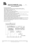
The Alignment of the BDM-Port Pads
On the most ECU Boards the location of
pin 1 of the BDM-port pads are not
marked in any way. This application
note will demonstrate how you can
estimate the location of Pin1 of the
BDM-port pads in the very most cases.
The figure on the right shows the
Motorola (TM) standard pinout of the
BDM-port:
VFLS0
GROUND
GROUND
HRESET
Power (+3.3 V)
1
3
5
7
9
2
4
6
8
10
SRESET
TCK/DSCK
VFLS1
TDI/DSDI
TDO/DSDO
Fig. 1: This is the standard BDM-port pinout.
Regarding the pinout of the standard
BDM-port it is obvious that two of them
are grounded. These are the pins 3 and
5. So the pin 1 is above them.
Which of the pads are grounded you can
find out simply using an ohmmeter or a
diode-tester.
Finally let us demonstrate this again in
the next three steps using a SMD
footprint of the BDM-port pads:
1st. step:
Fig. 2: This the typical arrangement of the BDM pads.
2nd. step:
Fig. 3: Then estimate which pads are grounded
2
4
6
8
10
1
3
5
7
9
3rd. step:
Fig. 4: The pin1 is left of the two grounded pins, as
agreed.
EVC electronic GmbH
-34-
BDM100 Module