1
Serial Peripheral Interface
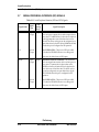
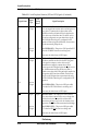
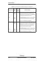
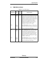
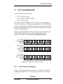
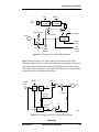
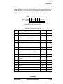
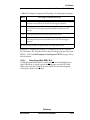
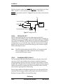
SPI Data and Control Pins
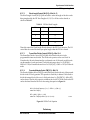
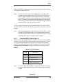
duration of the transaction. The SS line of the master must be held high. If it goes
low, a mode fault error flag (the MDF bit) is set in the SPSR. To disable the mode
fault circuit, program the SS pin as a GPIO pin in the PCC register. This inhibits
the mode fault flag, while the other three lines are dedicated to the SPI peripheral.
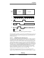
The state of the master and slave CPH bits (in the SPCR) affects the operation of
SS. The CPH bit settings should be the same for both master and slave. When the
CPH bit is cleared, the shift clock is the OR of SS with SCK. In this clock phase
mode, SS must go high between successive bytes in an SPI message. When the
CPH bit is set, SS can be left low between successive SPI bytes. In cases where
there is only one SPI slave MCU, its SS line can be tied to VSS as long as only
CPH = 1 clock mode is used. The SS0 pin can be programmed as a GPIO pin (PC3)
when the SPI SS0 function is not being used.
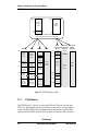
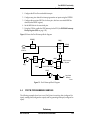
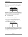
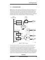
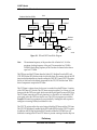
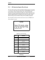
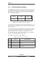
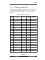
The four pins on SPI1 are as follows:
• MISO1/PC4 (SPI1 Master In Slave Out)—MISO1 is one of two unidirectional
serial data signals. It is an input to a master device and an output from a slave
device. If a slave device is not selected, the MISO0 line of the slave device is
placed in the high-impedance state. MISO1 can be programmed as a GPIO pin
called PC4 when the SPI MISO1 function is not being used.
• MOSI1/PC5 (SPI1 Master Out Slave In)—The MOSI1 line is the second of the
two unidirectional serial data signals. It is an output from a master device and an
input to a slave device. The master device places data on the MOSI1 line a
half-cycle before the clock edge that the slave device uses to latch the data. MOSI1
can be programmed as a GPIO pin called PC5 when the SPI MOSI1 function is not
being used.
• SCK1/PC6 (SPI1 Serial Clock)—SCK1, an input to a slave device, is generated by
the master device and synchronizes data movement in and out of the device
through the MOSI1 and MISO1 lines. Master and slave devices are capable of
exchanging a byte of information during a sequence of eight clock cycles. Slave
devices ignore the SCK signal unless the SS pin is active low.
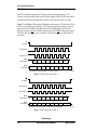
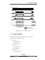
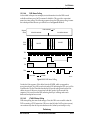
Four possible timing relationships can be chosen by using the CPL and CPH
control bits in the SPCR. Both master and slave devices must operate with the
same timing. The SPI clock rate select bits (SPR[2:0]) in the SPCR of the master
device select the clock rate. In a slave device, the SPR[2:0] bits have no effect on
the operation of the SPI. The SCK1 pin can be programmed as a GPIO pin (PC6)
when the SPI SCK1 function is not being used.
• SS1/PC7 F(SPI1 Slave Select)—The SS input of a slave device must be externally
asserted before a master device can exchange data with the slave device. SS must
be low before data transactions and must stay low for the duration of the
Preliminary
MOTOROLA
DSP56824 User’s Manual
7-13