1
OnCE Module
Command, Status, and Control Registers
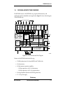
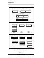
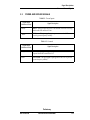
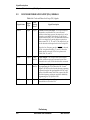
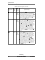
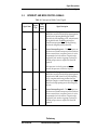
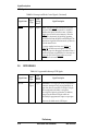
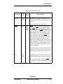
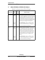
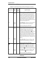
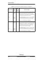
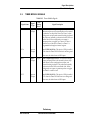
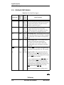
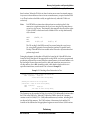
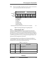
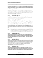
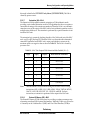
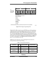
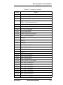
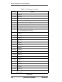
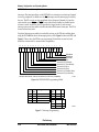
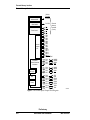
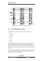
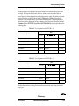
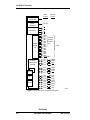
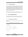
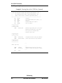
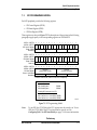
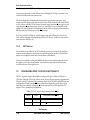
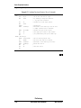
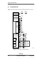
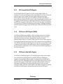
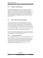
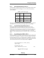
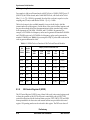
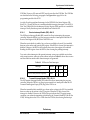
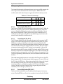
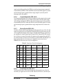
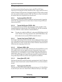
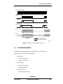
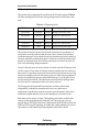
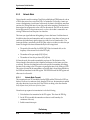
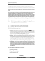
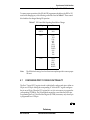
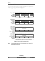
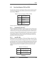
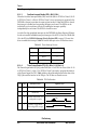
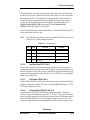
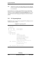
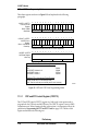
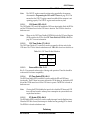
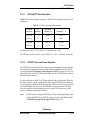
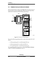
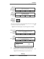
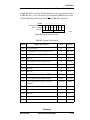
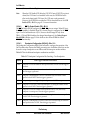
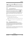
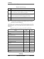
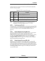
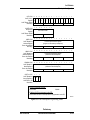
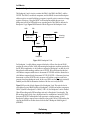
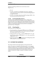
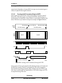
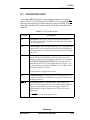
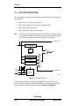
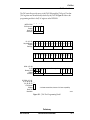
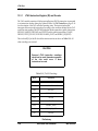
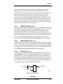
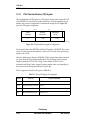
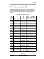
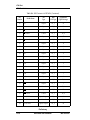
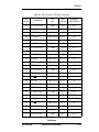
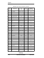
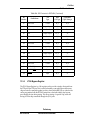
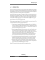
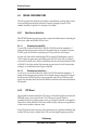
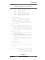
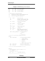
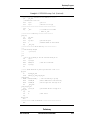
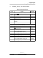
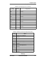
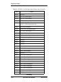
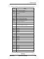
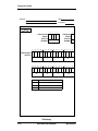
in Figure 12-5. The lowest five bits (RS[4:0]) identify the source for the operation, defined
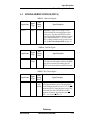
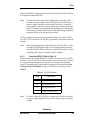
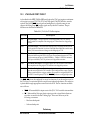
in Table 12-3. Bits 5, 6, and 7 define the Exit (EX) command bit (Table 12-4), the Execute
(GO) bit (Table 12-5), and the Read/Write (R/W) bit (Table 12-6), respectively.
OCMDR
OnCE Command Register
Reset: not modified
Write Only
7
6
5
R/W
GO
EX
4
3
2
1
0
RS4 RS3 RS2 RS1 RS0
AA0106
Figure 12-5 OnCE Command Format
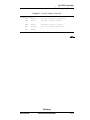
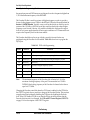
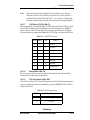
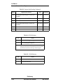
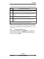
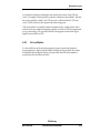
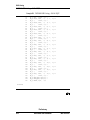
Table 12-3 Register Select Encoding
RS[4:0]
Register/Action Selected
Mode
Read/Write
00000
No register selected
All
N/A
00001
OnCE Breakpoint and Trace Counter (OCNTR)
All
Read/Write
00010
OnCE Debug Control Register (OCR)
All
R/W
00011
(Reserved)
All
N/A
00100
OnCE Breakpoint Address Register (OBAR)
All
Write-only
00101
(Reserved)
All
N/A
00110
(Reserved)
All
N/A
00111
(Reserved)
All
N/A
01000
OnCE PGDB Bus Transfer Register (OPGDBR)
Debug
Read-only
01001
OnCE Program Data Bus Register (OPDBR)
Debug
Read/Write
01010
OnCE Program Address Register—Fetch cycle
(OPABFR)
FIFO halted
Read-only
01011
(Reserved)
N/A
N/A
01100
Clear OCNTR
All
N/A
01101
(Reserved)
N/A
N/A
01110
(Reserved)
N/A
N/A
01111
(Reserved)
N/A
N/A
Preliminary
MOTOROLA
DSP56824 User’s Manual
12-15