1
AllenBradley
FLEX I/O Analog
Modules
User Manual
(Cat. No. 1794IE8, OE4,
and IE4XOE2 Series B)
File Name: AB_AnalogModule_1794_IEx_OEx_user_D596
Important User Information
Because of the variety of uses for the products described in this
publication, those responsible for the application and use of this control
equipment must satisfy themselves that all necessary steps have been taken
to assure that each application and use meets all performance and safety
requirements, including any applicable laws, regulations, codes
and standards.
The illustrations, charts, sample programs and layout examples shown in
this guide are intended solely for example. Since there are many variables
and requirements associated with any particular installation, Allen-Bradley
does not assume responsibility or liability (to include intellectual property
liability) for actual use based upon the examples shown in this publication.
Allen-Bradley publication SGI–1.1, “Safety Guidelines For The
Application, Installation and Maintenance of Solid State Control”
(available from your local Allen-Bradley office) describes some important
differences between solid-state equipment and electromechanical devices
which should be taken into consideration when applying products such as
those described in this publication.
Reproduction of the contents of this copyrighted publication, in whole or
in part, without written permission of Allen–Bradley Company, Inc.
is prohibited.
Throughout this manual we make notes to alert you to possible injury to
people or damage to equipment under specific circumstances.
ATTENTION: Identifies information about practices or
circumstances that can lead to personal injury or death, property
damage or economic loss.
Attention helps you:
Identify a hazard.
Avoid the hazard.
Recognize the consequences.
Important: Identifies information that is especially important for
successful application and understanding of the product.
Important: We recommend you frequently backup your application
programs on appropriate storage medium to avoid possible data loss.
Summary of Changes
This publication contains new and revised information not included
in the previous version.
New Information
Addition of DeviceNet Mapping
A new chapter has been added to describe the special mapping for
DeviceNet.
Additional Flex I/O Modules
New series B analog modules are now available for Flex I/O users.
These modules are:
• 1794-OE4 series B 4 output analog module
• 1794-IE8 series B 8 input analog module
• 1794-IE4XOE2 series B 4 in/2 out combo analog module
The differences between series A and series B are explained in
Appendix B.
I/O Mapping
I/O mapping for the series B versions of the analog modules has
been added.
Revised Information
This manual has been revised to include separate chapters for remote
I/O adapters and DeviceNet adapters. In addition, range selection bits
have been revised to include an Off condition.
Change Bars
The areas in this manual which are different from previous editions
are marked with change bars (as shown to the right of this paragraph)
to indicate the addition of new or revised information.
Publication 17946.5.2 - May 1996
Table of Contents
Summary of Changes . . . . . . . . . . . . . . . . . . . . . . . . . . . .
P1
New Information . . . . . . . . . . . . . . . . . . . . . . . . . . . . . . . . . . . . .
Addition of DeviceNet Mapping . . . . . . . . . . . . . . . . . . . . . . . .
Additional Flex I/O Modules . . . . . . . . . . . . . . . . . . . . . . . . . . .
I/O Mapping . . . . . . . . . . . . . . . . . . . . . . . . . . . . . . . . . . . . . .
Revised Information . . . . . . . . . . . . . . . . . . . . . . . . . . . . . . . . . .
Change Bars . . . . . . . . . . . . . . . . . . . . . . . . . . . . . . . . . . . . . . .
P1
P1
P1
P1
P1
P1
Using This Manual . . . . . . . . . . . . . . . . . . . . . . . . . . . . . . .
P-1
Purpose of this Manual . . . . . . . . . . . . . . . . . . . . . . . . . . . . . . . .
Audience . . . . . . . . . . . . . . . . . . . . . . . . . . . . . . . . . . . . . . . . . .
Vocabulary . . . . . . . . . . . . . . . . . . . . . . . . . . . . . . . . . . . . . . . .
Manual Organization . . . . . . . . . . . . . . . . . . . . . . . . . . . . . . . . .
Conventions . . . . . . . . . . . . . . . . . . . . . . . . . . . . . . . . . . . . . . .
For Additional Information . . . . . . . . . . . . . . . . . . . . . . . . . . . . . .
P-1
P-1
P-1
P-1
P-2
P-2
Overview of FLEX I/O and your Analog Modules . . . . . . . .
1-1
Chapter Objectives . . . . . . . . . . . . . . . . . . . . . . . . . . . . . . . . . . .
The FLEX I/O System . . . . . . . . . . . . . . . . . . . . . . . . . . . . . . . . .
Types of FLEX I/O Modules . . . . . . . . . . . . . . . . . . . . . . . . . . . . .
How FLEX I/O Analog Modules Communicate
with Programmable Controllers . . . . . . . . . . . . . . . . . . . . . . .
Features of your Analog Modules . . . . . . . . . . . . . . . . . . . . . . . .
Chapter Summary . . . . . . . . . . . . . . . . . . . . . . . . . . . . . . . . . . .
1-1
1-1
1-2
1-2
1-4
1-4
How to Install Your Analog Module . . . . . . . . . . . . . . . . . .
2-1
Chapter Objectives . . . . . . . . . . . . . . . . . . . . . . . . . . . . . . . . . . .
Before You Install Your Analog Module . . . . . . . . . . . . . . . . . . . . .
Compliance to European Union Directives . . . . . . . . . . . . . . . . . .
EMC Directive . . . . . . . . . . . . . . . . . . . . . . . . . . . . . . . . . . . .
Low Voltage Directive . . . . . . . . . . . . . . . . . . . . . . . . . . . . . . .
Power Requirements . . . . . . . . . . . . . . . . . . . . . . . . . . . . . . . . .
Installing the Module . . . . . . . . . . . . . . . . . . . . . . . . . . . . . . . . . .
Mounting the Terminal Base Unit on a DIN Rail . . . . . . . . . . . . .
Panel/Wall Mounting . . . . . . . . . . . . . . . . . . . . . . . . . . . . . . . .
Mounting the Analog Module on the Terminal Base Unit . . . . . . .
Connecting Wiring for the Analog Modules . . . . . . . . . . . . . . . . . .
Connecting Wiring using a 1794TB2 or TB3 Terminal Base Unit
Module Indicators . . . . . . . . . . . . . . . . . . . . . . . . . . . . . . . . . . . .
Chapter Summary . . . . . . . . . . . . . . . . . . . . . . . . . . . . . . . . . . .
2-1
2-1
2-1
2-1
2-2
2-2
2-4
2-4
2-5
2-7
2-8
2-9
2-13
2-13
ii
Table of Contents
Module Programming . . . . . . . . . . . . . . . . . . . . . . . . . . . .
3-1
Chapter Objectives . . . . . . . . . . . . . . . . . . . . . . . . . . . . . . . . . . .
Block Transfer Programming . . . . . . . . . . . . . . . . . . . . . . . . . . . .
Sample programs for Flex I/O Analog Modules . . . . . . . . . . . . . . .
PLC3 Programming . . . . . . . . . . . . . . . . . . . . . . . . . . . . . . . .
Figure 3.1
PLC3 Family Sample Program Structure for a 1794IE8 Module
Figure 3.2
PLC3 Family Sample Program Structure for a
1794OE4 Module . . . . . . . . . . . . . . . . . . . . . . . . . . . . . . . . .
Figure 3.3
PLC3 Family Sample Program Structure for a
1794IE4XOE2 Module . . . . . . . . . . . . . . . . . . . . . . . . . . . . .
PLC5 Programming . . . . . . . . . . . . . . . . . . . . . . . . . . . . . . . . .
Figure 3.4
PLC5 Family Sample Program Structure for the 1794IE8 . . . .
Figure 3.5
PLC5 Family Sample Program Structure for the 1794OE4 . . .
Figure 3.6
PLC5 Family Sample Program Structure for the 1794IE4XOE2
PLC2 Programming . . . . . . . . . . . . . . . . . . . . . . . . . . . . . . . . .
Analog Data Format . . . . . . . . . . . . . . . . . . . . . . . . . . . . . . . . . .
Chapter Summary . . . . . . . . . . . . . . . . . . . . . . . . . . . . . . . . . . .
3-1
3-1
3-2
3-2
Writing Configuration to and Reading Status from
Your Module with a Remote I/O Adapter . . . . . . . . . . .
Chapter Objectives . . . . . . . . . . . . . . . . . . . . . . . . . . . . . . . . . . .
Configuring Your Analog Module . . . . . . . . . . . . . . . . . . . . . . . . .
Range Selection . . . . . . . . . . . . . . . . . . . . . . . . . . . . . . . . . . . .
Safe State Value Selection . . . . . . . . . . . . . . . . . . . . . . . . . . . . .
Data Format . . . . . . . . . . . . . . . . . . . . . . . . . . . . . . . . . . . . . . .
Reading Data From Your Module . . . . . . . . . . . . . . . . . . . . . . . . .
Mapping Data for the Analog Modules . . . . . . . . . . . . . . . . . . . . .
8 Input Analog Module (Cat. No. 1794IE8 Series B) . . . . . . . . .
Analog Input Module (1794IE8) Read . . . . . . . . . . . . . . . . .
Word/Bit Descriptions for the 1794IE8 Analog
Input Module Read . . . . . . . . . . . . . . . . . . . . . . . . . . . .
Analog Input Module (1794IE8/B) Write Configuration Block .
Range Selection Bits for the 1794IE8/B Analog Input Module
Word/Bit Descriptions for the 1794IE8/B Analog Input
Module Write . . . . . . . . . . . . . . . . . . . . . . . . . . . . . . . .
4 Output Analog Module (Cat. No. 1794OE4 Series B) . . . . . . .
Analog Output Module (1794OE4/B) Read . . . . . . . . . . . . .
Bit/Word Descriptions for the 1794OE4/B Analog Output
Module Read . . . . . . . . . . . . . . . . . . . . . . . . . . . . . . . .
Analog Output Module (1794OE4/B) Write Configuration Block
3-2
3-3
3-3
3-4
3-4
3-4
3-5
3-5
3-6
3-6
4-1
4-1
4-1
4-2
4-2
4-2
4-2
4-3
4-3
4-3
4-4
4-4
4-5
4-5
4-6
4-6
4-6
4-7
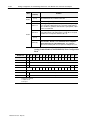
Table of Contents
Range Selection Bits for the 1794OE4/B Analog Output
Module (Word 5) . . . . . . . . . . . . . . . . . . . . . . . . . . . . . .
Word/Bit Descriptions for the 1794OE4/B Analog Output
Module Write . . . . . . . . . . . . . . . . . . . . . . . . . . . . . . . .
4 Input/2 Output Analog Combo Module
(Cat. No. 1794IE4XOE2 Series B) . . . . . . . . . . . . . . . . . . .
Analog Combo Module (1794IE4XOE2/B) Read . . . . . . . . .
Word/Bit Descriptions for the 1794IE4XOE2/B Analog Combo
Module Read . . . . . . . . . . . . . . . . . . . . . . . . . . . . . . . .
Analog Combo Module (1794IE4XOE2/B) Write
Configuration Block . . . . . . . . . . . . . . . . . . . . . . . . . . . .
Range Selection Bits for the 1794IE4XOE2/B Analog
Combo Module . . . . . . . . . . . . . . . . . . . . . . . . . . . . . . .
Word/Bit Descriptions for the 1794IE4XOE2/B Analog
Combo Module Write . . . . . . . . . . . . . . . . . . . . . . . . . . .
Chapter Summary . . . . . . . . . . . . . . . . . . . . . . . . . . . . . . . . . . .
How Communication Takes Place and I/O Image
Table Mapping with the DeviceNet Adapter . . . . . . . . .
Chapter Objectives . . . . . . . . . . . . . . . . . . . . . . . . . . . . . . . . . . .
About DeviceNet Manager . . . . . . . . . . . . . . . . . . . . . . . . . . . . .
Polled I/O Structure . . . . . . . . . . . . . . . . . . . . . . . . . . . . . . . . . .
Adapter Input Status Word . . . . . . . . . . . . . . . . . . . . . . . . . . .
Mapping Data into the Image Table . . . . . . . . . . . . . . . . . . . . . . .
8 Input Analog Module (Cat. No. 1794IE8 Series B)
Image Table Mapping . . . . . . . . . . . . . . . . . . . . . . . . . . . .
Analog Input Module (1794IE8/B) Read . . . . . . . . . . . . . . .
Analog Input Module (1794IE8/B) Write . . . . . . . . . . . . . . . .
Range Selection Bits for the 1794IE8/B Analog Input Module
Word/Bit Descriptions for the 1794IE8/B Analog Input Module
4 Output Analog Module (1794OE4 Series B) Image
Table Mapping . . . . . . . . . . . . . . . . . . . . . . . . . . . . . . . . .
Analog Output Module (1794OE4/B) Read . . . . . . . . . . . . .
Analog Output Module (1794OE4/B) Write . . . . . . . . . . . . . .
Range Selection Bits for the 1794OE4/B Analog Output
Module (Write Word 6) . . . . . . . . . . . . . . . . . . . . . . . . .
Word/Bit Descriptions for the 1794OE4/B Analog
Output Module . . . . . . . . . . . . . . . . . . . . . . . . . . . . . . .
Analog Combo Module (1794IE4XOE2 Series B)
Image Table Mapping . . . . . . . . . . . . . . . . . . . . . . . . . . . .
Analog Combo Module (1794IE4XOE2/B) Read . . . . . . . . .
Analog Output Module (1794IE4XOE2/B) Write . . . . . . . . . .
Range Selection Bits for the 1794IE4XOE2 Analog
Combo Module . . . . . . . . . . . . . . . . . . . . . . . . . . . . . . .
Word/Bit Descriptions for the 1794IE4XOE2 Analog
Combo Module . . . . . . . . . . . . . . . . . . . . . . . . . . . . . . .
Defaults . . . . . . . . . . . . . . . . . . . . . . . . . . . . . . . . . . . . . . . . . .
iii
4-7
4-7
4-9
4-9
4-9
4-10
4-11
4-11
4-12
5-1
5-1
5-1
5-1
5-2
5-3
5-3
5-3
5-4
5-4
5-4
5-6
5-6
5-6
5-7
5-7
5-9
5-9
5-10
5-10
5-10
5-12
iv
Table of Contents
Specifications . . . . . . . . . . . . . . . . . . . . . . . . . . . . . . . . . .
A-1
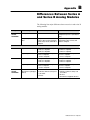
Differences Between Series A and Series B Analog Modules B-1
Data Table Formats . . . . . . . . . . . . . . . . . . . . . . . . . . . . . .
C-1
Two's Complement Binary . . . . . . . . . . . . . . . . . . . . . . . . . . . . . .
Analog Data Format . . . . . . . . . . . . . . . . . . . . . . . . . . . . . . . . . .
Scaling Example . . . . . . . . . . . . . . . . . . . . . . . . . . . . . . . . . .
Support Services . . . . . . . . . . . . . . . . . . . . . . . . . . . . . . . . . . . .
Technical Support . . . . . . . . . . . . . . . . . . . . . . . . . . . . . . . . .
Engineering and Field Services . . . . . . . . . . . . . . . . . . . . . . . .
Technical Training . . . . . . . . . . . . . . . . . . . . . . . . . . . . . . . . .
Repair and Exchange Services . . . . . . . . . . . . . . . . . . . . . . . .
C-1
C-2
C-3
C-1
C-1
C-1
C-1
C-1
Preface
Using This Manual
Purpose of this Manual
Audience
This manual shows you how to use your FLEX I/O Analog modules
with Allen-Bradley programmable controllers. The manual helps you
install, program and troubleshoot your modules.
You must be able to program and operate an Allen-Bradley
programmable controller to make efficient use of your FLEX I/O
modules. In particular, you must know how to program block
transfers.
We assume that you know how to do this in this manual. If you do
not, refer to the appropriate programming and operations manual
before you attempt to program your modules.
Vocabulary
In this manual, we refer to:
– the analog input or analog output module as the “input
module” or ‘‘output module”
– the Programmable Controller as the “controller”
Manual Organization
This manual is divided into five chapters. The following chart lists
each chapter with its corresponding title and a brief overview of the
topics covered in that chapter.
Chapter
Title
Contents
1
Overview of FLEX I/O and Analog Describes FLEX I/O Analog modules, features, and how
modules
they function
2
How to Install Your Analog
Module
How to install and wire the modules
3
Module Programming
Explains block transfer programming, sample programs
4
Writing Configuration to and
Reading Status From with a
Remote I/O Adapter
Explains how to configure your modules and read status
information from your modules when using a remote I/O
adapter
5
How Communication Takes Place
and I/O Image Table Mapping
with the DeviceNet Adapter
Explains how you communicate with your modules, and
how the I/O image is mapped when using a DeviceNet
adapter
Appendix
Title
Contents
A
Specifications
Specifications for the analog modules
B
Differences Between Series A
and Series B Analog Modules
Lists major differences between series.
C
Data Formats
Explains 2's complement and left justification of numbers
Publication 17946.5.2 - May 1996
P–2
Using This Manual
Conventions
We use these conventions in this manual:
In this manual, we show:
Like this:
that there is more information about a topic
in another chapter in this manual
that there is more information about the
topic in another manual
For Additional Information
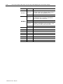
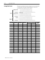
For additional information on FLEX I/O systems and modules, refer
to the following documents:
Catalog
Number
Publications
Voltage
1794
Description
Installation
Instructions
1794 FLEX I/O Product Data
17942.1
User
Manual
1794ACN
24V dc
ControlNet Adapter
17945.8
1794ADN
24V dc
DeviceNet Adapter
17945.14
17946.5.5
1794ASB
24V dc
17946.5.3
Remote I/O Adapter
17945.11
1794TB2
1794TB3
2wire Terminal Base
3wire Terminal Base
17945.2
1794TBN
Terminal Base Unit
17945.16
1794TBNF
Fused Terminal Base Unit
17945.17
1794TB3T
Temperature Terminal Base Unit
17945.41
1794IB16
24V dc
16 Input Module
17945.4
1794OB16
24V dc
16 Output Module
17945.3
1794IB10XOB6
24V dc
10 Input/6 Output Module
17945.24
1794IE8
24V dc
Selectable Analog 8 Input Module
17945.6
1794OE4
24V dc
Selectable Analog 4 Output Module
17945.5
1794IE4XOE2
24V dc
4 Input/2 Output Analog Module
17945.15
1794IR8
24V dc
8 RTD Input Analog Module
17945.22
17946.5.4
1794IT8
24V dc
8 Thermocouple Input Module
17945.21
17946.5.7
1794IB8S
24V dc
Sensor Input Module
17945.7
1794IA8
120V ac
8 Input Module
17945.9
1794OA8
120V ac
Output Module
17945.10
1794CE1
Extender Cable
17942.12
1794NM1
Mounting Kit
17942.13
Power Supply
17945.35
1794PS1
Publication 17946.5.2 - May 1996
More
24V dc
17946.5.2
1
Chapter
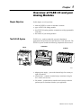
Overview of FLEX I/O and your
Analog Modules
Chapter Objectives
In this chapter, we tell you about:
• what the FLEX I/O system is and what it contains
• types of FLEX I/O analog modules
• how FLEX I/O analog modules communicate with programmable
controllers
• the features of your analog modules
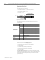
The FLEX I/O System
Adapter
FLEX I/O is a small, modular I/O system for distributed
applications that performs all of the functions of rack-based I/O. The
FLEX I/O system contains the following components shown below:
Terminal Base
I/O Module
5
I
V I
V
I
V
I
V I
V
I
V
20125
• adapter/power supply – powers the internal logic for as many as
eight I/O modules
• terminal base – contains a terminal strip to terminate wiring for
two- or three-wire devices
• I/O module – contains the bus interface and circuitry needed to
perform specific functions related to your application
Publication 17946.5.2 - May 1996
1–2
Overview of FLEX I/O and your Analog Modules
Types of FLEX I/O Modules
We describe the following FLEX I/O Analog modules in this user
manual:
Catalog Number
Voltage
Inputs
Outputs
Description
1794IE8
24V dc
8
-
analog - 8 input, singleended, non-isolated
1794OE4
24V dc
-
4
analog - 4 output, singleended, non-isolated
1794IE4XOE2
24V dc
4
2
analog - 4 input, singleended, non-isolated
and 2 output, singleended, nonisolated
FLEX I/O analog input, output and combination modules are block
transfer modules that interface analog signals with any
Allen-Bradley programmable controllers that have block transfer
capability. Block transfer programming moves input from the
module’s memory to a designated area in the processor data table,
and output data words from a designated area in the processor data
table to the module’s memory. Block transfer programming also
moves configuration words from the processor data table to module
memory.
The analog modules have selectable ranges as shown in the table
below:
How FLEX I/O Analog
Modules Communicate
with Programmable
Controllers
Publication 17946.5.2 - May 1996
Voltage
Current
0 to 10V dc
0 to 20mA
+/-10V dc
4 to 20mA
The adapter/power supply transfers data to the module (block
transfer write) and from the module (block transfer read) using BTW
and BTR instructions in your ladder diagram program. These
instructions let the adapter obtain input values and status from the
module, and let you send output values and establish the module’s
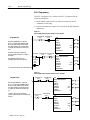
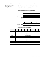
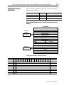
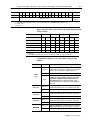
mode of operation. Figure 1.1 describes the communication process.
Overview of FLEX I/O and your Analog Modules
1–3
Figure 1.1
An Example of Communication Between an Adapter and an
Analog Input Module
1
2
The adapter transfers your configuration data
to the module using a BTW.
External devices transmit
analog signals to the module.
Flexbus
AllenBradley
AllenBradley
ADAPTER
ACTIVE
FAULT
LOCAL
FAULT
1794-IE8
ANALOG INPUT
24VDC
POWER SUPPLY
RIO ADAPTER
1794ASB
2
4
Your ladder program instructs the
adapter to perform a BTR of the values
and stores them in a data table.
INPUT 0 INPUT 1 INPUT 2 INPUT 3 INPUT 4 INPUT 5 INPUT 6 INPUT 7
V I
V I
V I
V I
V I
V I
V I
V
I
5
The adapter and module determine
that the transfer was made without error
and input values are within specified
range.
3
The module converts analog signals
into binary format and stores these
values until the adapter requests their
transfer.
6
Your ladder program can use and/or move the data (if valid)
before it is written over by the transfer of new data in a
subsequent transfer.
7
Your ladder program performs BTWs to the module when you power
it up, and any time you wish to reconfigure the module.
Publication 17946.5.2 - May 1996
1–4
Overview of FLEX I/O and your Analog Modules
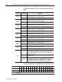
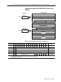
Features of your Analog
Modules
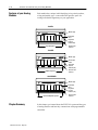
Each module has a unique label identifying its keyswitch position,
wiring and module type. A removable label provides space for
writing individual designations per your application.
1794IE8
AllenBradley
Module Type
1794-IE8
ANALOG INPUT
3
INPUT 0
V
I
INPUT 1
V
I
INPUT 2
V
I
INPUT 3
V
I
INPUT 4
V
I
INPUT 5
V
I
INPUT 6
V
I
INPUT 7
V
I
PWR
Removable
Label
Keyswitch
Position
Indicator (#3)
Green Power
Indicator
Input Designators
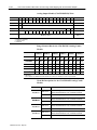
1794OE4
AllenBradley
Module Type
1794-OE4
ANALOG OUTPUT
Removable
Label
4
I
OUTPUT 0
RET V
RET
I
OUTPUT 1
RET V
RET
I
OUTPUT 2
RET V
RET
I
OUTPUT 3
RET V
RET
PWR
Keyswitch
Position
Indicator (#4)
Green Power
Indicator
Output Designators
1794IE4XOE2
Module Type
AllenBradley
1794-IE4XOE2
ANALOG COMBO
5
INPUT 0
V
I
INPUT 1
V
I
INPUT 2
V
I
INPUT 3
V
I
I
OUTPUT 0
RET V
RET
I
OUTPUT 1
RET V
RET
V
Input and Output Designators
Chapter Summary
Publication 17946.5.2 - May 1996
PWR
Removable
Label
Keyswitch
Position
Indicator (#5)
Green Power
Indicator
In this chapter you learned about the FLEX I/O system and the types
of analog modules and how they communicate with programmable
controllers.
Chapter
2
How to Install Your
Analog Module
Chapter Objectives
In this chapter, we tell you about:
•
•
•
•
Before You Install Your
Analog Module
how to install your module
how to set the module keyswitch
how to wire the terminal base
the indicators
Before installing your analog module in the I/O chassis:
You need to:
Calculate the power requirements of all
modules in each chassis.
Power Requirements, page 2-2
Position the keyswitch on the terminal base
Installing the Module, page 2-4
!
Compliance to
European Union Directives
As described under:
ATTENTION: +24V dc power must be applied to
your module before operation. If power is not applied,
the module position will appear to the adapter as an
empty slot in your chassis. If the adapter does not
recognize your module after installation is completed,
cycle power to the adapter.
If this product has the CE mark it is approved for installation within
the European Union and EEA regions. It has been designed and
tested to meet the following directives.
EMC Directive
This product is tested to meet Council Directive 89/336/EEC
Electromagnetic Compatibility (EMC) and the following standards,
in whole or in part, documented in a technical construction file:
• EN 50081-2EMC – Generic Emission Standard, Part 2 –
Industrial Environment
• EN 50082-2EMC – Generic Immunity Standard, Part 2 –
Industrial Environment
This product is intended for use in an industrial environment.
Publication 17946.5.2 - May 1996
2–2
How to Install Your Analog Module
Low Voltage Directive
This product is tested to meet Council Directive 73/23/EEC
Low Voltage, by applying the safety requirements of EN 61131–2
Programmable Controllers, Part 2 – Equipment Requirements and
Tests.
For specific information required by EN 61131-2, see the appropriate
sections in this publication, as well as the following Allen-Bradley
publications:
• Industrial Automation Wiring and Grounding Guidelines For
Noise Immunity, publication 1770-4.1
• Guidelines for Handling Lithium Batteries, publication AG-5.4
• Automation Systems Catalog, publication B111
Power Requirements
The wiring of the terminal base unit is determined by the current
draw through the terminal base. Make certain that the current draw
does not exceed 10A.
!
Publication 17946.5.2 - May 1996
ATTENTION: Total current draw through the
terminal base unit is limited to 10A. Separate power
connections may be necessary.
How to Install Your Analog Module
2–3
Methods of wiring the terminal base units are shown in the
illustration below.
!
ATTENTION: Do not daisy chain power or
ground from an analog terminal base unit to any ac
or dc discrete module terminal base unit.
Analog Module
Analog Module
Analog Module
Analog Module
Daisychaining
24V dc
Note: All modules must be analog modules for this configuration.
Wiring when total current draw is less than 10A
Discrete
Module
Individual
Analog Module
Discrete
Module
Discrete
Module
24V dc
24V dc or
120V ac
Note: Use this configuration if using any
noisy" dc discrete I/O modules in your system.
24V dc
Analog module wiring separate from discrete wiring.
Wiring when total current draw is greater than 10A
Discrete
Module
Combination
Analog Module
Analog Module
Analog Module
24V dc
24V dc
Note: All modules powered by the same power supply
must be analog modules for this configuration.
Total current draw through any base unit must not be greater than 10A
Publication 17946.5.2 - May 1996
2–4
How to Install Your Analog Module
Installing the Module
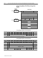
Installation of the analog module consists of:
• mounting the terminal base unit
• installing the analog module into the terminal base unit
• installing the connecting wiring to the terminal base unit
If you are installing your module into a terminal base unit that is
already installed, proceed to “Mounting the Analog Module on the
Terminal Base” on page 2–7.
Mounting the Terminal Base Unit on a DIN Rail
!
ATTENTION: Do not remove or replace a terminal
base unit when power is applied. Interruption of the
flexbus can result in unintended operation or machine
motion.
1. Remove the cover plug (if used) in the male connector of the unit
to which you are connecting this terminal base unit.
2. Check to make sure that the 16 pins in the male connector on the
adjacent device are straight and in line so that the mating female
connector on this terminal base unit will mate correctly.
3. Position the terminal base on the 35 x 7.5mm DIN rail A (A-B pt.
no. 199-DR1; 46277-3; EN 50022) at a slight angle with hook B
on the left side of the terminal base hooked into the right side of
the unit on the left.
A
B
D
C
A
D
4. Make certain that the female flexbus connector C is fully
retracted into the base unit.
Publication 17946.5.2 - May 1996
How to Install Your Analog Module
2–5
5. Rotate the terminal base onto the DIN rail with the top of the rail
hooked under the lip on the rear of the terminal base. Use caution
to make sure that the female flexbus connector does not strike
any of the pins in the mating male connector.
6. Press the terminal base down onto the DIN rail until flush. The
locking tab D will snap into position and lock the terminal base to
the DIN rail.
7. If the terminal base does not lock in place, use a screwdriver or
similar device to move the locking tab down, press the terminal
base flush with the DIN rail and release the locking tab to lock
the base in place.
8. Gently push the female flexbus connector C into the adjacent
terminal base or adapter female connector to complete the flexbus
connections.
9. Repeat the above steps to install the next terminal base.
Panel/Wall Mounting
Installation on a wall or panel consists of:
•
•
•
•
laying out the drilling points on the wall or panel
drilling the pilot holes for the mounting screws
mounting the adapter mounting plate
installing the terminal base units and securing them to the wall or
panel
If you are installing your module into a terminal base unit that is
already installed, proceed to “Mounting the Analog Module on the
Terminal Base” on page 2–7.
Use the mounting kit Cat. No. 1794-NM1 for panel/wall mounting.
1.4
(35.5)
1794NM1 Mounting Kit
Contents:
1 - Mounting Plate for Adapter
2 - 18 #6 selftapping screws
(2 for the adapter, and 2
each for up to 8 modules)
1
2
Adapter Module
(not included)
Terminal Base Unit
(not included)
Publication 17946.5.2 - May 1996
2–6
How to Install Your Analog Module
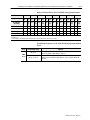
To install the mounting plate on a wall or panel:
1. Lay out the required points on the wall/panel as shown in the
drilling dimension drawing.
Drilling Dimensions for Panel/Wall Mounting of FLEX I/O
Inches
(Millimeters)
1.4
(35.5)
2.3
(58.5)
1.4
(35.5)
2.3
(58.5)
1.4
(35.5)
.83 (21)
2. Drill the necessary holes for the #6 self-tapping mounting screws.
3. Mount the mounting plate (1) for the adapter module using two
#6 self-tapping screws (18 included for mounting up to 8 modules
and the adapter).
Important:
More
Make certain that the mounting plate is properly
grounded to the panel. Refer to “Industrial Automation
Wiring and Grounding Guidelines,” publication
1770-4.1.
4. Hold the adapter (2) at a slight angle and engage the top of the
mounting plate in the indention on the rear of the adapter module.
5. Press the adapter down flush with the panel until the locking lever
locks.
6. Position the terminal base unit up against the adapter and push the
female bus connector into the adapter.
7. Secure to the wall with two #6 self-tapping screws.
8. Repeat for each remaining terminal base unit.
Note: The adapter is capable of addressing eight modules. Do not
exceed a maximum of eight terminal base units in your system.
Publication 17946.5.2 - May 1996
How to Install Your Analog Module
2–7
Mounting the Analog Module on the Terminal Base Unit
1. Rotate the keyswitch (1) on the terminal base unit (2) clockwise
to the position required for the specific type of analog module.
7
3
1
2
6
4
5
Analog Module Cat. No.
Keyswitch Position
1794IE8
3
1794OE4
4
1794IE4XOE2
5
2. Make certain the flexbus connector (3) is pushed all the way to
the left to connect with the neighboring terminal base/adapter.
You cannot install the module unless the connector is fully
extended.
3. Make sure that the pins on the bottom of the module are straight
so they will align properly with the connector in the terminal base
unit.
4. Position the module (4) with its alignment bar (5) aligned with
the groove (6) on the terminal base.
5. Press firmly and evenly to seat the module in the terminal base
unit. The module is seated when the latching mechanism (7) is
locked into the module.
6. Repeat the above steps to install the next module in its terminal
base unit.
Publication 17946.5.2 - May 1996
2–8
How to Install Your Analog Module
ATTENTION: Remove field-side power before
removing or inserting the module. This module is
designed so you can remove and insert it under
backplane power. When you remove or insert a module
with field-side power applied, an electrical arc may
occur. An electrical arc can cause personal injury or
property damage by:
!
• sending an erroneous signal to your system’s field
devices causing unintended machine motion
• causing an explosion in a hazardous environment
Repeated electrical arcing causes excessive wear to
contacts on both the module and its mating connector.
Worn contacts may create electrical resistance.
Wiring to the analog modules is made through the terminal base unit
on which the module mounts.
Refer to the following table for recommended terminal base units
that you can use for each module.
Publication 17946.5.2 - May 1996
Module
1794TB2
1794TB3
1794IE8
Yes
Yes
1794OE4
Yes
Yes
1794IE4XOE2
Yes
Yes
+RZ WR ,QVWDOO <RXU $QDORJ 0RGXOH
ï
&RQQHFWLQJ :LULQJ XVLQJ D 7% RU 7% 7HUPLQDO %DVH 8QLW
&RQQHFW WKH LQGLYLGXDO VLJQDO ZLULQJ WR QXPEHUHG WHUPLQDOV RQ
WKH ï URZ $ RQ WKH WHUPLQDO EDVH XQLW 8VH %HOGHQ FDEOH IRU VLJQDO ZLULQJ
$77(17,21 &RQQHFW RQO\ RQH FXUUHQW RU RQH
YROWDJH VLJQDO SHU FKDQQHO 'R QRW FRQQHFW ERWK FXUUHQW
DQG YROWDJH RQ RQH FKDQQHO
&RQQHFW HDFK FKDQQHO FRPPRQ WR
,( ï WKH DVVRFLDWHG WHUPLQDO RQ URZ %
2( ï WKH FRUUHVSRQGLQJ WHUPLQDO RQ WKH VDPH URZ $
,(;2( ï LQSXWV ï WKH DVVRFLDWHG WHUPLQDO RQ URZ %
RXWSXWV ï WKH FRUUHVSRQGLQJ WHUPLQDO RQ WKH VDPH URZ $ &RQQHFW 9 GF WR WHUPLQDO RQ WKH URZ & DQG 9
FRPPRQ WR WHUPLQDO RQ WKH ï URZ % $77(17,21 7R UHGXFH VXVFHSWLELOLW\ WR QRLVH
SRZHU DQDORJ PRGXOHV DQG GLVFUHWH PRGXOHV IURP
VHSDUDWH SRZHU VXSSOLHV 'R QRW H[FHHG D OHQJWK RI IW P IRU GF SRZHU FDEOLQJ
$77(17,21 5HPRYH ILHOGVLGH SRZHU EHIRUH
UHPRYLQJ RU LQVHUWLQJ WKH PRGXOH 7KLV PRGXOH LV
GHVLJQHG VR \RX FDQ UHPRYH DQG LQVHUW LW XQGHU
EDFNSODQH SRZHU :KHQ \RX UHPRYH RU LQVHUW D PRGXOH
ZLWK ILHOGVLGH SRZHU DSSOLHG DQ HOHFWULFDO DUF PD\
RFFXU $Q HOHFWULFDO DUF FDQ FDXVH SHUVRQDO LQMXU\ RU
SURSHUW\ GDPDJH E\
VHQGLQJ DQ HUURQHRXV VLJQDO WR \RXU V\VWHP·V ILHOG
GHYLFHV FDXVLQJ XQLQWHQGHG PDFKLQH PRWLRQ
FDXVLQJ DQ H[SORVLRQ LQ D KD]DUGRXV HQYLURQPHQW
5HSHDWHG HOHFWULFDO DUFLQJ FDXVHV H[FHVVLYH ZHDU WR
FRQWDFWV RQ ERWK WKH PRGXOH DQG LWV PDWLQJ FRQQHFWRU
:RUQ FRQWDFWV PD\ FUHDWH HOHFWULFDO UHVLVWDQFH
7%
7%
&
ï $
ï $
ï %
ï %
ï &
3XEOLFDWLRQ ï
+RZ WR ,QVWDOO <RXU $QDORJ 0RGXOH
,I GDLV\ FKDLQLQJ WKH 9 GF SRZHU WR WKH QH[W EDVH XQLW
FRQQHFW D MXPSHU IURP WHUPLQDO RQ WKLV EDVH XQLW WR WHUPLQDO
RQ WKH QH[W EDVH XQLW &RQQHFW WKH 9 GF FRPPRQUHWXUQ
IURP WHUPLQDO RQ WKLV EDVH XQLW WR WHUPLQDO RQ WKH QH[W EDVH
XQLW
$77(17,21 9 GF SRZHU PXVW EH DSSOLHG WR
\RXU PRGXOH EHIRUH RSHUDWLRQ ,I SRZHU LV QRW DSSOLHG
WKH PRGXOH SRVLWLRQ ZLOO DSSHDU WR WKH DGDSWHU DV DQ
HPSW\ VORW LQ \RXU FKDVVLV ,I WKH DGDSWHU GRHV QRW
UHFRJQL]H \RXU PRGXOH DIWHU LQVWDOODWLRQ LV FRPSOHWHG
F\FOH SRZHU WR WKH DGDSWHU
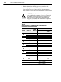
7DEOH $
:LULQJ FRQQHFWLRQV IRU 7% DQG 7% 7HUPLQDO %DVH 8QLWV
ZKHQ XVLQJ WKH ,( $QDORJ 0RGXOH
&KDQQHO
3XEOLFDWLRQ 6LJQDO 7\SH
/DEHO
0DUNLQJV
&XUUHQW
7% 7%
6LJQDO 7HUPLQDO
9 GF &RPPRQ
7HUPLQDO
,
9ROWDJH
9
&XUUHQW
,
9ROWDJH
9
&XUUHQW
,
9ROWDJH
9
&XUUHQW
,
9ROWDJH
9
&XUUHQW
,
9ROWDJH
9
&XUUHQW
,
9ROWDJH
9
&XUUHQW
,
9ROWDJH
9
&XUUHQW
,
9ROWDJH
9
9 GF &RPPRQ
WKUX 9 GF SRZHU
7% ï DQG 7% ï WKUX 7HUPLQDOV WKUX DUH LQWHUQDOO\ FRQQHFWHG LQ WKH WHUPLQDO EDVH XQLW
+RZ WR ,QVWDOO <RXU $QDORJ 0RGXOH
ï
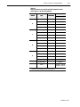
7DEOH %
:LULQJ FRQQHFWLRQV IRU 7% DQG 7% 7HUPLQDO %DVH 8QLWV
ZKHQ XVLQJ WKH 2( $QDORJ 0RGXOH
&KDQQHO
7% 7%
7\SH
/DEHO 0DUNLQJ
&XUUHQW 6LJQDO
,
&XUUHQW &RPPRQ
5(7
9ROWDJH 6LJQDO
9
9ROWDJH &RPPRQ
5(7
&XUUHQW 6LJQDO
,
&XUUHQW &RPPRQ
5(7
9ROWDJH 6LJQDO
9
9ROWDJH &RPPRQ
5(7
&XUUHQW 6LJQDO
,
&XUUHQW &RPPRQ
5(7
9ROWDJH 6LJQDO
9
9ROWDJH &RPPRQ
5(7
&XUUHQW 6LJQDO
,
&XUUHQW &RPPRQ
5(7
9ROWDJH 6LJQDO
9
9ROWDJH &RPPRQ
5(7
6LJQDO 7HUPLQDO
9 GF &RPPRQ
WKUX 9 GF
7% ï DQG 7% ï WKUX 7HUPLQDOV DQG DUH LQWHUQDOO\ FRQQHFWHG LQ WKH PRGXOH WR 9 GF FRPPRQ
7HUPLQDOV WKUX DUH LQWHUQDOO\ FRQQHFWHG LQ WKH WHUPLQDO EDVH XQLW
3XEOLFDWLRQ ï
+RZ WR ,QVWDOO <RXU $QDORJ 0RGXOH
7DEOH &
:LULQJ FRQQHFWLRQV IRU 7% DQG 7% 7HUPLQDO %DVH 8QLWV
ZKHQ XVLQJ WKH ,(;2( $QDORJ 0RGXOH
&KDQQHO
6LJQDO 7\SH
/DEHO
0DUNLQJV
7% 7%
6LJQDO 7HUPLQDO
9 GF &RPPRQ
7HUPLQDO
,QSXW
&XUUHQW
,
9ROWDJH
9
&XUUHQW
,
9ROWDJH
9
&XUUHQW
,
9ROWDJH
9
&XUUHQW
,
9ROWDJH
9
2XWSXW
&XUUHQW 6LJQDO
&XUUHQW &RPPRQ
9ROWDJH 6LJQDO
9ROWDJH &RPPRQ
&XUUHQW 6LJQDO
&XUUHQW &RPPRQ
9ROWDJH 6LJQDO
9ROWDJH &RPPRQ
9 GF &RPPRQ
9 GF SRZHU
5(7
9
5(7
,
5(7
9
5(7
WKUX 7% ï DQG 7% ï WKUX 7HUPLQDOV DQG DUH LQWHUQDOO\ FRQQHFWHG LQ WKH PRGXOH WR 9 GF FRPPRQ
7HUPLQDOV WKUX DUH LQWHUQDOO\ FRQQHFWHG LQ WKH WHUPLQDO EDVH XQLW
3XEOLFDWLRQ ,
$77(17,21 7RWDO FXUUHQW GUDZ WKURXJK WKH
WHUPLQDO EDVH XQLW LV OLPLWHG WR $ 6HSDUDWH SRZHU
FRQQHFWLRQV WR WKH WHUPLQDO EDVH XQLW PD\ EH QHFHVVDU\
+RZ WR ,QVWDOO <RXU $QDORJ 0RGXOH
0RGXOH ,QGLFDWRUV
ï
7KH DQDORJ PRGXOHV KDYH RQH VWDWXV LQGLFDWRU WKDW LV RQ ZKHQ SRZHU
LV DSSOLHG WR WKH PRGXOH
$OOHQ%UDGOH\
ï,(
$1$/2* ,1387
,1387 ,1387 ,1387 ,1387 ,1387 ,1387 ,1387 ,1387 3:5
9 ,
9 ,
9 ,
9 ,
9 ,
9 ,
9 ,
9
,
,(
$OOHQ%UDGOH\
ï2(
$1$/2* 287387
,
287387 5(7 9 5(7 ,
287387 5(7 9 5(7 ,
287387 5(7 9 5(7
,
6WDWXV ,QGLFDWRU ï
,QGLFDWHV SRZHU DSSOLHG
WR PRGXOH
3:5
287387 5(7 9 5(7
2(
$OOHQ%UDGOH\
$1$/2* &20%2
ï,(;2(
,1387 ,1387 ,1387 ,1387 9 ,
9 ,
9 ,
9 ,
,
287387 5(7 9 5(7 ,
287387 5(7 9 5(7
3:5
,(;2(
&KDSWHU 6XPPDU\
,Q WKLV FKDSWHU \RX OHDUQHG KRZ WR LQVWDOO \RXU LQSXW PRGXOH LQ DQ
H[LVWLQJ SURJUDPPDEOH FRQWUROOHU V\VWHP DQG KRZ WR ZLUH WR WKH
WHUPLQDO EDVH XQLWV
3XEOLFDWLRQ Chapter
3
Module Programming
Chapter Objectives
In this chapter, we tell you about:
• analog data format
• block transfer programming
• sample programs for the PLC-3 and PLC-5 processors
Block Transfer
Programming
Your module communicates with the processor through bidirectional
block transfers. This is the sequential operation of both read and
write block transfer instructions.
A configuration block transfer write (BTW) is initiated when the
analog module is first powered up, and subsequently only when the
programmer wants to enable or disable features of the module. The
configuration BTW sets the bits which enable the programmable
features of the module, such as scaling, alarms, ranges, etc. Block
transfer reads are performed to retrieve information from the module.
Block transfer read (BTR) programming moves status and data from
the module to the processor’s data table. The processor user program
initiates the request to transfer data from the module to the processor.
The transferred words contain module status, channel status and
input data from the module.
!
ATTENTION: If the analog module is not powered
up before the remote I/O adapter, the adapter will not
recognize the module. Make certain that the analog
module is installed and powered before or
simultaneously with the remote I/O adapter. If the
adapter does not establish communication with the
module, cycle power to the adapter.
The following sample programs are minimum programs; all rungs
and conditioning must be included in your application program. You
can disable BTRs, or add interlocks to prevent writes if desired. Do
not eliminate any storage bits or interlocks included in the sample
programs. If interlocks are removed, the program may not work
properly.
Your program should monitor status bits, block transfer read and
block transfer write activity.
Publication 17946.5.2 - May 1996
3–2
Module Programming
Sample programs for Flex
I/O Analog Modules
The following sample programs show you how to use your analog
module efficiently when operating with a programmable controller.
These programs show you how to:
• configure the module
• read data from the module
• update the module’s output channels (if used)
These programs illustrate the minimum programming required for
communication to take place.
PLC3 Programming
Block transfer instructions with the PLC-3 processor use one binary
file in a data table section for module location and other related data.
This is the block transfer control file. The block transfer data file
stores data that you want transferred to your module (when
programming a block transfer write) or from your module (when
programming a block transfer read). The address of the block
transfer data files are stored in the block transfer control file.
The same block transfer control file is used for both the read and
write instructions for your module. A different block transfer
control file is required for every module.
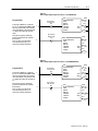
A sample program segment with block transfer instructions is shown
in Figure 3.1, and described below.
Figure 3.1
PLC3 Family Sample Program Structure for a 1794IE8 Module
Enable
BTR
Program Action
Block Transfer
Read Done Bit
B3:0
At powerup in RUN mode, or when the
1
processor is switched from PROG to RUN,
the user program enables a block transfer
read. Then it initiates a block transfer write
to configure the module if the powerup bit
is set.
Thereafter, the program continuously
performs read block transfers.
Note: You must create the data file
for the block transfers before you
enter the block transfer instructions.
15
Pushbutton
2
Block Transfer
Write Done Bit
B3:0
05
B4:8
DN
15
Error
ER
Enable
BTW
BLOCK XFER WRITE
RACK:
GROUP:
MODULE:
CONTROL:
DATA FILE:
LENGTH:
15
1 Powerup
Publication 17946.5.2 - May 1996
7
0
0
#B3:0
#B4:0
9
EN
12
Done
13
Powerup Bit1
The pushbutton allows the user to
manually request a block transfer write to
configure the module.
BLOCK XFER READ
RACK:
GROUP:
MODULE:
CONTROL:
DATA FILE:
LENGTH:
7
0
0
#B3:0
#B5:0
1
EN
02
Done
DN
05
Error
ER
03
bit included in Series B modules only.
Module Programming
3–3
Figure 3.2
PLC3 Family Sample Program Structure for a 1794OE4 Module
Enable
BTR
Program Action
At powerup in RUN mode, or when the
processor is switched from PROG to RUN,
the user program enables a block transfer
read. Then it initiates a block transfer write
to configure the module and send data
values.
Thereafter, the program continuously
performs read block transfers and write
block transfers.
Note: You must create the data file
for the block transfers before you
enter the block transfer instructions.
1
Block Transfer
Read Done Bit
B6:0
15
BLOCK XFER READ
RACK:
GROUP:
MODULE:
CONTROL:
DATA FILE:
LENGTH:
7
1
0
#B6:0
#B7:0
1
EN
12
Done
DN
15
Error
ER
13
Block Transfer
Write Done Bit
B6:0
2
05
Enable
BTW
BLOCK XFER WRITE
RACK:
GROUP:
MODULE:
CONTROL:
DATA FILE:
LENGTH:
7
1
0
#B6:0
#B8:0
14
EN
02
Done
DN
05
Error
ER
03
Figure 3.3
PLC3 Family Sample Program Structure for a 1794IE4XOE2 Module
Enable
BTR
Program Action
At powerup in RUN mode, or when the
1
processor is switched from PROG to RUN,
the user program enables a block transfer
read. Then it initiates a block transfer write
to configure the module and send data val
ues
Thereafter, the program continuously
performs read block transfers and write
block transfers.
Note: You must create the data file
for the block transfers before you
enter the block transfer instructions.
2
Block Transfer
Read Done Bit
B9:0
15
BLOCK XFER READ
RACK:
GROUP:
MODULE:
CONTROL:
DATA FILE:
LENGTH:
7
2
0
#B9:0
#B10:0
5
EN
12
Done
DN
15
Error
ER
13
Block Transfer
Write Done Bit
B9:0
05
Enable
BTW
BLOCK XFER WRITE
RACK:
GROUP:
MODULE:
CONTROL:
DATA FILE:
LENGTH:
7
2
0
#B9:0
#B11:0
8
EN
02
Done
DN
05
Error
ER
03
Publication 17946.5.2 - May 1996
3–4
Module Programming
PLC5 Programming
The PLC-5 program is very similar to the PLC-3 program with the
following exceptions:
• block transfer enable bits are used instead of done bits as the
conditions on each rung.
• separate block transfer control files are used for the block transfer
instructions.
Figure 3.4
PLC5 Family Sample Program Structure for the 1794IE8
BTW Enable Bit BTR Enable Bit
N12:0
N12:5
Program Action
1
Thereafter, the program continuously
performs read block transfers to configure
the module.
Pushbutton
2
BTR Enable Bit BTW Enable Bit
N12:0
N12:5
15
The pushbutton allows the user to
manually request a block transfer write.
15
Powerup
Bit1
N13:8
1 Powerup
bit included in Series B modules only.
15
EN
2
1
0
N12:0
N13:0
9
N
RACK:
GROUP:
MODULE:
CONTROL:
DATA FILE:
LENGTH:
CONTINUOUS:
15
15
At powerup in RUN mode, or when the
processor is switched from PROG to RUN,
the user program enables a block transfer
read. Then it initiates a block transfer write
to configure the module if the powerup bit
is set.
BTR
BLOCK TRANSFER READ
DN
ER
BTW
BLOCK TRANSFER WRITE
RACK:
GROUP:
MODULE:
CONTROL:
DATA FILE:
LENGTH:
CONTINUOUS:
EN
2
1
0
N12:5
N13:20
1
N
DN
ER
Figure 3.5
PLC5 Family Sample Program Structure for the 1794OE4
Program Action
1
BTR Enable Bit
N14:0
15
At powerup in RUN mode, or when the
processor is switched from PROG to RUN,
the user program enables a block transfer
read. Then it initiates a block transfer write
to configure the module and send data val
ues.
Thereafter, the program continuously
performs read block transfers and write block
transfers.
2
BTW Enable Bit
N14:5
15
Publication 17946.5.2 - May 1996
BTW Enable Bit
N14:5
15
BTR Enable Bit
N14:0
15
BTR
BLOCK TRANSFER READ
RACK:
GROUP:
MODULE:
CONTROL:
DATA FILE:
LENGTH:
CONTINUOUS:
2
2
0
N14:0
N15:0
1
N
BTW
BLOCK TRANSFER WRITE
RACK:
GROUP:
MODULE:
CONTROL:
DATA FILE:
LENGTH:
CONTINUOUS:
2
2
0
N14:5
N15:5
14
N
EN
DN
ER
EN
DN
ER
Module Programming
3–5
Figure 3.6
PLC5 Family Sample Program Structure for the 1794IE4XOE2
Program Action
1
At powerup in RUN mode, or when the
processor is switched from PROG to RUN,
the user program enables a block transfer
read. Then it initiates a block transfer write
to configure the module and send data
values.
Thereafter, the program continuously
performs read block transfers and write block
transfers.
2
BTW Enable Bit
N16:5
15
BTR Enable Bit
N16:0
15
BTR Enable Bit
N16:0
15
BTW Enable Bit
N16:5
15
BTR
BLOCK TRANSFER READ
2
3
0
N16:0
N17:0
5
N
RACK:
GROUP:
MODULE:
CONTROL:
DATA FILE:
LENGTH:
CONTINUOUS:
BTW
BLOCK TRANSFER WRITE
RACK:
GROUP:
MODULE:
CONTROL:
DATA FILE:
LENGTH:
CONTINUOUS:
2
3
0
N16:5
N17:5
8
N
EN
DN
ER
EN
DN
ER
PLC2 Programming
The 1794 analog I/O modules are not recommended for use with
PLC-2 family programmable controllers due to the number of digits
needed for high resolution. In addition, the data returned from the
analog-to-digital converter in the module is 12-bit resolute. This
value is left-justified into a 16-bit field, reserving the most
significant bit for a sign bit. Refer to Appendix B for more
information.
Publication 17946.5.2 - May 1996
3–6
Module Programming
Analog Data Format
The data returned from the analog-to-digital converter in the module
is 12-bit resolute. This value is left-justified into a 16-bit field,
reserving the most significant bit for a sign bit.
11 10 09 08 07 06 05 04 03 02 01 00
A/D Unipolar Data
Analog Value
Input
A/D Bipolar Data
Analog Value
Output
D/A Data
Analog Value
⇓ ⇓ ⇓⇓ ⇓ ⇓ ⇓ ⇓⇓ ⇓ ⇓⇓
0* 14 13 12 11 10 09 08 07 06 05 04 03 02 01 00
* = Always positive
S 10 09 08 07 06 05 04 03 02 01 00
⇓ ⇓ ⇓⇓ ⇓ ⇓ ⇓ ⇓⇓ ⇓ ⇓⇓
S
14 13 12 11 10 09 08 07 06 05 04 03 02 01 00
S
11 10 09 08 07 06 05 04 03 02 01 00
S
14 13 12 11 10 09 08 07 06 05 04 03 02 01 00
⇓ ⇓ ⇓⇓ ⇓ ⇓ ⇓ ⇓⇓ ⇓ ⇓⇓ ⇓
Refer to Appendix C for a table of values for various current and
voltage modes.
Appendix C also includes an example of scaling.
Chapter Summary
Publication 17946.5.2 - May 1996
In this chapter, you learned how to program your programmable
controller. You were given sample programs for your PLC-3 and
PLC-5 family processors.
Chapter
4
Writing Configuration to and
Reading Status from Your
Module with a Remote I/O
Adapter
Chapter Objectives
In this chapter, we tell you about:
•
•
•
•
Configuring Your Analog
Module
configuring your module’s features
entering your data
reading data from your module
read block format
Because of the many analog devices available and the wide variety
of possible configurations, you must configure your module to
conform to the analog device and specific application that you have
chosen. The module is configured using a group of data table words
that are transferred to the module using a block transfer write
instruction.
The software configurable features available are:
• input/output range selection, including full range and bipolar
• safe state operating value (customer selected analog values the
module will maintain in the event of a network communication
error)
Note: PLC-5 family programmable controllers that use 6200
software programming tools can take advantage of the IOCONFIG
utility to configure these modules. IOCONFIG uses menu-based
screens for configuration without having to set individual bits in
particular locations. Refer to your 6200 software literature for
details.
Publication 17946.5.2 - May 1996
4–2
Writing Configuration to and Reading Status from Your Module with a Remote I/O Adapter
Range Selection
Individual input channels are configurable to operate with the
following voltage or current ranges:
Bit Settings
1
Ranges
Configure
Select
Full Range
0-10V dc/0-20mA
0
1
4-20mA
1
0
10 to +10V dc
1
1
Off
0
0
When configured to Off, individual output channels will drive 0V/0mA.
!
ATTENTION: If using Series A modules, do not use
configure select and full range bit settings of 0.
Individual channels revert to 4–20mA with bit
selections of all zeroes. This could result in unwanted
or incorrect action.
You can select individual channel ranges using the designated words
of the write block transfer instruction. Refer to the Bit/Word
description for your particular module for word and bit numbers.
Safe State Value Selection
Data Format
You can select the analog values that your output module will
maintain in the event of a network communication error. When the
multiplex control bits (M) are cleared simultaneously by a
communication error, (or by the user), the analog outputs will
automatically switch to the values set in the safe state analog words.
This allows you to define a safe operating state for controlled
devices which depend on the analog output from the module.
The data returned from the analog-to-digital converter in the module
is 12-bit resolute. This value is left-justified into a 16-bit field,
reserving the most significant bit for a sign bit. The 4–20mA mode
scales in the module and uses all 16 bits.
Refer to Appendix C for a table of values for various current and
voltage modes, and an example of scaling to engineering terms.
Reading Data From Your
Module
Publication 17946.5.2 - May 1996
Read programming moves status and data from the module to the
processor’s data table. The processor’s user program initiates the
request to transfer data from the input module to the processor.
Configuring Your Module and Reading Status from Your Module with a Remote I/O Adapter
Mapping Data for the
Analog Modules
4–3
The following read and write words and bit/word descriptions
describe the information written to and read from the analog
modules. Each word is composed of 16 bits.
8 Input Analog Module (Cat. No. 1794IE8 Series B)
Module Image
Input Data Channel 0
Input Data Channel 1
I/O Image
Input Data Channel 2
Input Size
Input Data Channel 3
Input Data Channel 4
1 to 9 Words
Input Data Channel 5
Input Data Channel 6
Input Data Channel 7
Underrange
PU
Output Size
Configure select
0 or 1 Word
Analog Input Module (1794-IE8) Read
Word/Dec. Bit
15
14
13
12
11
10
09
08
07
06
05
04
03
02
01
00
Word/Octal Bit
17
16
15
14
13
12
11
10
07
06
05
04
03
02
01
00
Read Word 0
S
Analog Value Channel 0
Word 1
S
Analog Value Channel 1
Word 2
S
Analog Value Channel 2
Word 3
S
Analog Value Channel 3
Word 4
S
Analog Value Channel 4
Word 5
S
Analog Value Channel 5
Word 6
S
Analog Value Channel 6
Word 7
S
Analog Value Channel 7
Word 8
PU
U4
U3
U2
U1
U0
Where:
Not used - set to zero
U7
U6
U5
S = sign bit (in 2's complement)
U = Underrange bits for 420mA inputs
PU = Power up bit
Publication 17946.5.2 - May 1996
4–4
Writing Configuration to and Reading Status from Your Module with a Remote I/O Adapter
Word/Bit Descriptions for the 1794-IE8 Analog Input Module
Read
Decimal Bit
(Octal Bit)
Word
Read Word 0
Word 1
Word 2
Word 3
Word 4
Word 5
Word 6
Word 7
Definition
Bits 00-14
(00-16)
Channel 0 analog data - 12bit left justified two's complement number;
unused lower bits are zero; 420mA uses all 16 bits.
Bits 15 (17)
Channel 0 analog data sign bit.
Bits 00-14
(00-16)
Channel 1 analog data - 12bit left justified two's complement number;
unused lower bits are zero; 420mA uses all 16 bits.
Bits 15 (17)
Channel 1 analog data sign bit.
Bits 00-14
(00-16)
Channel 2 analog data - 12bit left justified two's complement number;
unused lower bits are zero; 420mA uses all 16 bits.
Bits 15 (17)
Channel 2 analog data sign bit.
Bits 00-14
(00-16)
Channel 3 analog data - 12bit left justified two's complement number;
unused lower bits are zero; 420mA uses all 16 bits.
Bits 15 (17)
Channel 3 analog data sign bit.
Bits 00-14
(00-16)
Channel 4 analog data - 12bit left justified two's complement number;
unused lower bits are zero; 420mA uses all 16 bits.
Bits 15 (17)
Channel 4 analog data sign bit.
Bits 00-14
(00-16)
Channel 5 analog data - 12bit left justified two's complement number;
unused lower bits are zero; 420mA uses all 16 bits.
Bits 15 (17)
Channel 5 analog data sign bit.
Bits 00-14
(00-16)
Channel 6 analog data - 12bit left justified two's complement number;
unused lower bits are zero; 420mA uses all 16 bits.
Bits 15 (17)
Channel 6 analog data sign bit.
Bits 00-14
(00-16)
Channel 7 analog data - 12bit left justified two's complement number;
unused lower bits are zero; 420mA uses all 16 bits.
Bits 15 (17)
Channel 7 analog data sign bit.
Bits 00-07
Underrange bits (U) for individual channels (420mA current input only)Bit 00 corresponds to input channel 0, bit 01 corresponds to input channel 1,
and so on. When set (1), indicates either a broken or open input wire, or input
current at or below 4mA.
Bits 0814
(1016)
Not used - set to 0.
Bit 15 (17)
Power Up bit - included in series B modules only. This bit is always 0 in
series A modules. This bit is set to 1 when all bits in the configuration
register (write word 0) are 0 (unconfigured state). The configuration
register can be cleared by either a reset, or by the user writing all zeroes to it.
Word 8
Analog Input Module (1794-IE8/B) Write Configuration Block
Word/Dec. Bit
15
14
13
12
11
10
09
08
07
06
05
04
03
02
01
00
Word/Octal Bit
17
16
15
14
13
12
11
10
07
06
05
04
03
02
01
00
Write Word 0
C7
C6
C5
C4
C3
C2
C1
C0
F7
F6
F5
F4
F3
F2
F1
F0
Where:
C = Configure select bit
F = Full range bit
Publication 17946.5.2 - May 1996
Configuring Your Module and Reading Status from Your Module with a Remote I/O Adapter
4–5
Range Selection Bits for the 1794-IE8/B Analog Input Module
Channel No.
Channel 0
Channel 1
Channel 2
Channel 3
Channel 4
Channel 5
Channel 6
Channel 7
F0
C0
F1
C1
F2
C2
F3
C3
F4
C4
F5
C5
F6
C6
F7
C7
Decimal Bits
(Octal Bits)
00
08
(10)
01
09
(11)
02
10
(12)
03
11
(13)
04
12
(14)
05
13
(15)
06
14
(16)
07
15
(17)
0-10V dc/0-20mA
1
0
1
0
1
0
1
0
1
0
1
0
1
0
1
0
4-20mA
0
1
0
1
0
1
0
1
0
1
0
1
0
1
0
1
10 to +10V dc
1
1
1
1
1
1
1
1
1
1
1
1
1
1
1
1
Off1
0
0
0
0
0
0
0
0
0
0
0
0
0
0
0
0
C = Configure select bit
F = Full range bit
1 When configured to off, individual channels will return 0000H on Series B modules, and 4 to 20mA on Series A modules.
Word/Bit Descriptions for the 1794-IE8/B Analog Input Module
Write
Word
Write
Word 0
Decimal Bit (Octal Bit)
Definition
Bits 00-07
Full range bits (F) for individual channels - Bit 00 corresponds to input channel
0, bit 01 corresponds to input channel 1, and so on.
Bits 08-15 (1017)
Configure select bits (C) for individual channels - Bit 08 corresponds to input
channel 0, bit 09 corresponds to input channel 1, and so on. Refer to Range Bit
Selections.
Publication 17946.5.2 - May 1996
4–6
Writing Configuration to and Reading Status from Your Module with a Remote I/O Adapter
4 Output Analog Module (Cat. No. 1794OE4 Series B)
I/O Image
Input Size
Module Image
0 or 1 Word
Read
PU
Diagnostics
Not used
Analog Data Channel 0
Analog Data Channel 1
Analog Data Channel 2
Analog Data Channel 3
Not used
Output Size
Write
M
Full Range
Config. Select
Not used
Not used
Not used
1 to 14 Words
Not used
Not used
Not used
Channel 0 Safe State
Channel 1 Safe State
Channel 2 Safe State
Channel 3 Safe State
Analog Output Module (1794-OE4/B) Read
Word/Dec. Bit
15
14
13
12
11
10
09
08
07
06
05
04
03
02
01
00
Word/Octal Bit
17
16
15
14
13
12
11
10
07
06
05
04
03
02
01
00
Read Word 0
PU
W3
W2
W1
W0
Where:
Not used - set to 0
W = Diagnostic bits for current output wire broken or load resistance high. (Not used on voltage outputs.)
PU = Power up bit
Bit/Word Descriptions for the 1794-OE4/B Analog Output
Module Read
Word
Read
Word 0
Publication 17946.5.2 - May 1996
Decimal Bit
(Octal Bit)
Definition
Bits 0003
Current outputs only - When set (1), the wire on the output is broken or the
load resistance is too high. Bit 00 corresponds to channel 0, bit 01
corresponds to channel 2, and so on.
Bits 0414
(04-16)
Not used - set to 0
Bit 15 (17)
Power Up bit - included in series B modules only. This bit is always 0 in
series A modules. This bit is set to 1 when all bits in the configuration
register (write word 5) are 0 (unconfigured state). The configuration
register can be cleared by either a reset, or by the user writing all zeroes to it.
Configuring Your Module and Reading Status from Your Module with a Remote I/O Adapter
4–7
Analog Output Module (1794-OE4/B) Write Configuration
Block
Word/Dec. Bit
15
14
13
12
11
10
09
08
07
06
05
04
03
02
01
00
Word/Octal Bit
17
16
15
14
13
12
11
10
07
06
05
04
03
02
01
00
Write Word 0
S
Analog Data - Channel 0
Word 1
S
Analog Data - Channel 1
Word 2
S
Analog Data - Channel 2
Word 3
S
Analog Data - Channel 3
Word 4
0
M3
M2
M1
M0
Word 5
0
F3
F2
F1
F0
Not used - set to 0
Not used - set to 0
C3
C2
Word 6 thru 9
C1
C0
Not used - set to 0
Not used - set to 0
Word 10
S
Safe State Value - Channel 0
Word 11
S
Safe State Value - Channel 1
Word 12
S
Safe State Value - Channel 2
Word 13
S
Safe State Value - Channel 3
Where:
S = Sign bit (in 2's complement)
M = Multiplex control
C = Configure select bit
F = Full range bit
Range Selection Bits for the 1794-OE4/B Analog Output Module
(Word 5)
Channel No.
Channel 0
Channel 1
Channel 2
Channel 3
F0
C0
F1
C1
F2
C2
F3
C3
Decimal Bits (Octal Bits)
00
08 (10)
01
09 (11)
02
10 (12)
03
11 (13)
4-20mA
0
1
0
1
0
1
0
1
0-10V dc/0-20mA
1
0
1
0
1
0
1
0
10 to +10V dc
1
1
1
1
1
1
1
1
Off1
0
0
0
0
0
0
0
0
C = Configure select bit
F = Full range bit
1 When configured to off, individual channels will send 0V or 0mV on Series B modules. On Series A modules, 2V or 4mA is output
until the module is configured.
Word/Bit Descriptions for the 1794-OE4/B Analog Output
Module Write
Word
Write Word
0
Decimal Bit
(Octal Bit)
Definition
Bits 00-14
(00-16)
Channel 0 analog data - 12bit left justified two's complement number; unused
lower bits are zero; 420mA uses all 16 bits.
Bits 15 (17)
Channel 0 analog data sign bit.
Publication 17946.5.2 - May 1996
4–8
Writing Configuration to and Reading Status from Your Module with a Remote I/O Adapter
Word
Decimal Bit
(Octal Bit)
Definition
Word 1
Bits 00-14
(00-16)
Channel 1 analog data - 12bit left justified two's complement number; unused
lower bits are zero; 420mA uses all 16 bits.
Bits 15 (17)
Channel 1 analog data sign bit.
Bits 00-14
(00-16)
Channel 2 analog data - 12bit left justified two's complement number; unused
lower bits are zero; 420mA uses all 16 bits.
Bits 15 (17)
Channel 2 analog data sign bit.
Bits 00-14
(00-16)
Channel 3 analog data - 12bit left justified two's complement number; unused
lower bits are zero; 420mA uses all 16 bits.
Bits 15 (17)
Channel 3 analog data sign bit.
Bits 00-03
Multiplex control bits (M) for individual channels. These bits control the safe
state analog outputs. - Bit 00 corresponds to output channel 0, bit 01
corresponds to output channel 1, and so on.
1 = use words 0, 1, 2 or 3 as directed by channel number n
0 = use words 10, 11, 12 or 13 as directed by channel number n
When bits 0003 are all cleared (0) simultaneously by a communication error or
user choice thru the programmable controller program, word 5 full range and
configure select bits are preserved at their last setting.
Bits 0415
(0417)
Not used - set to 0.
Bits 00-03
Full range bits (F) for individual channels - Bit 00 corresponds to output channel
0, bit 01 corresponds to output channel 1, and so on.
Bits 0407
Not used - set to 0.
Bits 08-11
(1013)
Configure select bits (C) for individual channels - Bit 08 corresponds to output
channel 0, bit 09 corresponds to output channel 1, and so on.
Bits 1215
(1417)
Not used - set to 0.
Words 6
thru 9
Bits 00-15
(00-17)
Not used - set to 0.
Word 10
Bits 00-14
(00-16)
Channel 0 Safe State analog value - 12bit left justified two's complement
number; unused lower bits are zero; 420mA uses all 16 bits.
Bits 15 (17)
Channel 0 Safe State analog data sign bit.
Bits 00-14
(00-16)
Channel 1 Safe State analog value - 12bit left justified two's complement
number; unused lower bits are zero; 420mA uses all 16 bits.
Bits 15 (17)
Channel 1 Safe State analog data sign bit.
Bits 00-14
(00-16)
Channel 2 Safe State analog value - 12bit left justified two's complement
number; unused lower bits are zero; 420mA uses all 16 bits.
Bits 15 (17)
Channel 2 Safe State analog data sign bit.
Bits 00-14
(00-16)
Channel 3 Safe State analog value - 12bit left justified two's complement
number; unused lower bits are zero; 420mA uses all 16 bits.
Bits 15 (17)
Channel 3 Safe State analog data sign bit.
Word 2
Word 3
Word 4
Word 5
Word 11
Word 12
Word 13
Publication 17946.5.2 - May 1996
Configuring Your Module and Reading Status from Your Module with a Remote I/O Adapter
4–9
4 Input/2 Output Analog Combo Module (Cat. No. 1794IE4XOE2 Series B)
Module Image
I/O Image
Input Data Channel 0
Input Size
Input Data Channel 1
0 to 5 Words
Read
Input Data Channel 2
Input Data Channel 3
Underrange & Diag.
PU
Output Data Channel 0
Output Data Channel 1
M
Not used
Not used
Output Size
Write
Full Range and Configure Select
Not used
0 to 8 Words
Not used
Output Channel 0 Safe State
Output Channel 1 Safe State
Analog Combo Module (1794-IE4XOE2/B) Read
Word/Dec. Bit
15
14
13
12
11
10
09
08
07
06
05
04
03
02
01
00
Word/Octal Bit
17
16
15
14
13
12
11
10
07
06
05
04
03
02
01
00
Read Word 0
S
Analog Value Input Channel 0
Word 1
S
Analog Value Input Channel 1
Word 2
S
Analog Value Input Channel 2
Word 3
S
Analog Value Input Channel 3
Word 4
PU
W0
U3
U2
U1
U0
Where:
Not used - set to 0
W1
S = sign bit (in 2's complement)
W = Diagnostic bits for current output wire broken or load resistance high. (Not used on voltage outputs.)
U = Underrange bits for 420mA inputs
PU = Power up bit
Word/Bit Descriptions for the 1794-IE4XOE2/B Analog Combo
Module Read
Word
Read
Word 0
Word 1
Word 2
Decimal Bit
(Octal Bit)
Definition
Bits 00-14
(00-16)
Channel 0 analog data - 12bit left justified two's complement number;
unused lower bits are zero; 420mA uses all 16 bits.
Bits 15 (17)
Channel 0 analog data sign bit.
Bits 00-14
(00-16)
Channel 1 analog data - 12bit left justified two's complement number;
unused lower bits are zero; 420mA uses all 16 bits.
Bits 15 (17)
Channel 1 analog data sign bit.
Bits 00-14
(00-16)
Channel 2 analog data - 12bit left justified two's complement number;
unused lower bits are zero; 420mA uses all 16 bits.
Bits 15 (17)
Channel 2 analog data sign bit.
Publication 17946.5.2 - May 1996
4–10
Writing Configuration to and Reading Status from Your Module with a Remote I/O Adapter
Word
Decimal Bit
(Octal Bit)
Word 3
Bits 00-14
(00-16)
Channel 3 analog data - 12bit left justified two's complement number;
unused lower bits are zero; 420mA uses all 16 bits.
Bits 15 (17)
Channel 3 analog data sign bit.
Bits 00-03
Underrange bits (U) for individual channels (420mA current inputs only) Bit 00 corresponds to input channel 0, bit 01 corresponds to input channel 1,
and so on. When set (1), indicates either a broken or open input wire, or input
current is at or below 4mA.
Bits 0405
Wire Off bits (W) - Current outputs only - When set (1), the wire on the
current output is broken or the load resistance is too high. Bit 00 corresponds
to channel 0, bit 01 corresponds to channel 2, and so on.
Bits 06-14
(06-16)
Not used
Bit 15 (17)
Power Up bit - included in series B modules only. This bit is always 0 in
series A modules. This bit is set to 1 when all bits in the configuration
register (write word 3) are 0 (unconfigured state). The configuration
register can be cleared by either a reset, or by the user writing all zeroes to it.
Word 4
Definition
Analog Combo Module (1794-IE4XOE2/B) Write Configuration
Block
Word/Dec. Bit
15
14
13
12
11
10
09
08
07
06
05
04
03
02
01
00
Word/Octal Bit
17
16
15
14
13
12
11
10
07
06
05
04
03
02
01
00
Write Word 0
S
Analog Data - Output Channel 0
Word 1
S
Analog Data - Output Channel 1
Word 2
0
Not used - set to 0
M1
M0
Word 3
Not used
F1
F0
Words 4 and 5
Where:
C5
C4
C3
C2
C1
C0
0
0
F5
F4
Not used - set to 0
Word 6
S
Safe State Value - Output Channel 0
Word 7
S
Safe State Value - Output Channel 1
M = Multiplex control bits
S = Sign bit (in 2's complement)
C = Configure select bit
F = Full range bit
Publication 17946.5.2 - May 1996
F3
F2
Configuring Your Module and Reading Status from Your Module with a Remote I/O Adapter
4–11
Range Selection Bits for the 1794-IE4XOE2/B Analog Combo
Module
Channel No.
Input
Channel 0
Input
Channel 1
Input
Channel 2
Input
Channel 3
Output
Channel 0
Output
Channel 1
F0
C0
F1
C1
F2
C2
F3
C3
F4
C4
F5
C5
Decimal Bits
(Octal Bits)
00
08
(10)
01
09
(11)
02
10
(12)
03
11
(13)
04
12
(14)
05
13
(15)
4-20mA
0
1
0
1
0
1
0
1
0
1
0
1
0-10V dc/0-20mA
1
0
1
0
1
0
1
0
1
0
1
0
10 to +10V dc
1
1
1
1
1
1
1
1
1
1
1
1
Off1
0
0
0
0
0
0
0
0
0
0
0
0
C = Configure select bit
F = Full range bit
1 When configured to off, individual channels will return or send either 0V or 0mA on Series B modules. On Series modules, 2V or 4mA is output
until the module is configured.
Word/Bit Descriptions for the 1794-IE4XOE2/B Analog Combo
Module Write
Word
Write
Word 0
Word 1
Decimal Bit
(Octal Bit)
Bits 00-14
(00-16)
Bits 15
(17)
Bits 00-14
(00-16)
Bits 15
(17)
Definition
Channel 0 analog data - 12bit left justified two's complement number; unused
lower bits are zero; 420mA uses all 16 bits.
Channel 0 analog data sign bit.
Channel 1 analog data - 12bit left justified two's complement number; unused
lower bits are zero; 420mA uses all 16 bits.
Channel 1 analog data sign bit.
Bits 00-01
Multiplex control bits (M) for individual channels. These bits control the safe state
analog outputs - Bit 00 corresponds to output channel 0, and bit 01 corresponds to
output channel 1.
1 = use words 0 and 1 (analog value) as directed by channel number n
0 = use words 6 and 7 (safe state analog value) as directed by channel number n
When bits 0001 are all cleared (0) simultaneously by a communication error or user
choice thru the programmable controller program, word 3 full range and configure
select bits are preserved at their last setting.
Bits 02-15
(02-17)
Not used - set to 0.
Bits 00-05
Full range bits (F) for individual channels - Bit 00 corresponds to input channel 0,
bit 01 corresponds to input channel 1, bit 02 corresponds to input channel 3, bit 03
corresponds to input channel 3, bit 04 corresponds to output channel 1, and bit 05
corresponds to output channel 2. Refer to Range Bit Selections.
Bits 0607
Not used - set to 0.
Bits 08-13
(1015)
Configure select bits (C) for individual channels - Bit 08 corresponds to input
channel 0, bit 09 (11) corresponds to input channel 1, bit 10 (12) corresponds to
input channel 2, bit 11 (13) corresponds to input channel 3, bit 12 (14) corresponds
to output channel 0, and bit 13 (15) corresponds to output channel 1. Refer to Range
Bit Selections.
Bits 1415
(1617)
Not used - set to 0.
Word 2
Word 3
Publication 17946.5.2 - May 1996
4–12
Writing Configuration to and Reading Status from Your Module with a Remote I/O Adapter
Word
Decimal Bit
(Octal Bit)
Words 4
and 5
Word 6
Word 7
Chapter Summary
Publication 17946.5.2 - May 1996
Definition
Not used - set to 0.
Bits 00-14
(00-16)
Channel 0 Safe State analog value - 12bit left justified two's complement number;
unused lower bits are zero; 420mA uses all 16 bits.
Bits 15 (17)
Channel 0 Safe State analog data sign bit.
Bits 00-14
(00-16)
Channel 1 Safe State analog value - 12bit left justified two's complement number;
unused lower bits are zero; 420mA uses all 16 bits.
Bits 15 (17)
Channel 1 Safe State analog data sign bit.
In this chapter you learned how to configure your module’s features
and enter your data.
Chapter
5
How Communication Takes
Place and I/O Image Table
Mapping with the DeviceNet
Adapter
Chapter Objectives
In this chapter you will learn about:
•
•
•
•
About DeviceNet Manager
DeviceNet Manager software
I/O structure
image table mapping
factory defaults
DeviceNet Manager is a software tool used to configure your FLEX
I/O DeviceNet adapter and its related modules. This software tool
can be connected to the adapter via the DeviceNet network.
You must know and understand how DeviceNet Manager works in
order to add a device to the network. Refer to the DeviceNet
Manager Software User Manual, publication 1787-6.5.3.
More
Polled I/O Structure
Output data is received by the adapter in the order of the installed
I/O modules. The Output data for Slot 0 is received first, followed
by the Output data for Slot 1, and so on up to slot 7.
The first word of input data sent by the adapter is the Adapter Status
Word. This is followed by the input data from each slot, in the order
of the installed I/O modules. The Input data from Slot 0 is first after
the status word, followed by Input data from Slot 2, and so on up to
slot 7.
DeviceNet Adapter
Read Data
Adapter Status
Slot 0 Input Data
Network READ
Slot 1 Input Data
...
...
Slot 7 Input Data
Read
Write Data
Write
I/O Module I/O Module
Slot 0
Slot 1
...
I/O Module
Slot 7
Slot 0 Output Data
Slot 1 Output Data
...
...
Network WRITE
Slot 7 Output Data
Publication 17946.5.2 - May 1996
5–2
How Communication Takes Place and I/O Image Table Mapping with the DeviceNet Adapter
Adapter Input Status Word
The input status word consists of:
• I/O module fault bits – 1 status bit for each slot
• node address changed – 1 bit
• I/O status – 1 bit
I/O Module Fault Bits
Slot 0
1 0
Slot 1
Slot 2
Not Used
Slot 3
9 8 7 6 5 4 3 2
Slot 5
Slot 4
10 through 15
Slot 6
15
Slot 7
Bit:
I/O State Bit
Node Address Changed Bit
The adapter input status word bit descriptions are shown in the
following table.
Bit Description
Bit
Explanation
0
This bit is set (1) when an error is detected in slot position 0.
1
This bit is set (1) when an error is detected in slot position 1.
2
This bit is set (1) when an error is detected in slot position 2.
3
This bit is set (1) when an error is detected in slot position 3.
4
This bit is set (1) when an error is detected in slot position 4.
5
This bit is set (1) when an error is detected in slot position 5.
6
This bit is set (1) when an error is detected in slot position 6.
7
This bit is set (1) when an error is detected in slot position 7.
Node Address Changed
8
This bit is set (1) when the node address switch setting has been
changed since power up.
I/O State
9
Bit = 0 - idle
Bit = 1 - run
I/O Module Fault
10 thru 15
Not used - sent as zeroes.
Possible causes for an I/O Module Fault are:
•
•
•
•
•
transmission errors on the FLEX I/O backplane
a failed module
a module removed from its terminal base
incorrect module inserted in a slot position
the slot is empty
The node address changed bit is set when the node address switch
setting has been changed since power up. The new node address does
not take affect until the adapter has been powered down and then
powered back up.
Publication 17946.5.2 - May 1996
How Communication Takes Place and I/O Image Table Mapping with the DeviceNet Adapter
Mapping Data into the
Image Table
5–33
FLEX I/O analog modules are supported by the DeviceNet adapter.
At present, these consist of:
Module Description
Catalog Number:
For image table mapping refer to:
8 Input Analog Module
1794IE8/B
page 5-3
4 Output Analog Module
1794OE4/B
page 5-6
4 in/2 out Analog Combo Module
1794IE4XOE2/B
page 5-9
8 Input Analog Module (Cat. No. 1794IE8 Series B) Image Table
Mapping
Module Image
Input Data Channel 0
Input Data Channel 1
I/O Image
Input Data Channel 2
Input Size
Input Data Channel 3
Input Data Channel 4
1 to 9 Words
Input Data Channel 5
Input Data Channel 6
Input Data Channel 7
Underrange
PU
Configure select
Not used
Output Size
Not used
0 or 1 Word
Not used
Not used
Not used
Analog Input Module (1794-IE8/B) Read
Decimal Bit
15
14
13
12
11
10
09
08
07
06
05
04
03
02
01
00
Size
Octal Bit
17
16
15
14
13
12
11
10
07
06
05
04
03
02
01
00
Read Words
S
Analog Value Channel 0
Read Word 1
S
Analog Value Channel 1
Read Word 2
S
Analog Value Channel 2
Read Word 3
S
Analog Value Channel 3
Read Word 4
S
Analog Value Channel 4
Read Word 5
S
Analog Value Channel 5
Read Word 6
S
Analog Value Channel 6
Read Word 7
Publication 17946.5.2 - May 1996
5–4
How Communication Takes Place and I/O Image Table Mapping with the DeviceNet Adapter
Decimal Bit
15
14
13
12
11
10
09
08
07
06
05
04
03
02
01
00
Size
Octal Bit
17
16
15
14
13
12
11
10
07
06
05
04
03
02
01
00
Read Words
S
Analog Value Channel 7
PU
Where:
Not used - set to zero
U7
U6
U5
Read Word 8
U4
U3
U2
U1
U0
Read Word 9
PU = Power up bit - included in series B modules only.
U = Underrange bits for 420mA inputs
S = sign bit (in 2's complement)
Analog Input Module (1794-IE8/B) Write
Decimal Bit
15
14
13
12
11
10
09
08
07
06
05
04
03
02
01
00
Size
Octal Bit
17
16
15
14
13
12
11
10
07
06
05
04
03
02
01
00
Write Words
C7
C6
C5
C4
C3
C2
C1
C0
F7
F6
F5
F4
F3
F2
F1
F0
Write Word 1
Not used - set to 0
Where:
Write Word 2 thru 6
C = Configure select bit
F = Full range bit
Range Selection Bits for the 1794-IE8/B Analog Input Module
Channel No.
Channel 0
Channel 1
Channel 2
Channel 3
Channel 4
Channel 5
Channel 6
Channel 7
F0
C0
F1
C1
F2
C2
F3
C3
F4
C4
F5
C5
F6
C6
F7
C7
Decimal Bit
00
08
01
09
02
10
03
11
04
12
05
13
06
14
07
15
0-10V dc/0-20mA
1
0
1
0
1
0
1
0
1
0
1
0
1
0
1
0
4-20mA
0
1
0
1
0
1
0
1
0
1
0
1
0
1
0
1
10 to +10V dc
1
1
1
1
1
1
1
1
1
1
1
1
1
1
1
1
Off1
0
0
0
0
0
0
0
0
0
0
0
0
0
0
0
0
C = Configure select bit
F = Full range bit
1 When configured to off, individual channels will return 0000H on Series B modules, and 420mA on Series A modules.
Word/Bit Descriptions for the 1794-IE8/B Analog Input Module
Word
Read Word 1
Decimal Bit
Definition
Bits 00-14
Channel 0 analog data - 12bit left justified two's complement
number; unused lower bits are zero; 420mA uses all 16 bits.
Bits 15
Read Word 2
Bits 00-14
Bits 15
Read Word 3
Bits 00-14
Bits 15
Read Word 4
Bits 00-14
Bits 15
Publication 17946.5.2 - May 1996
Channel 0 analog data sign bit.
Channel 1 analog data - 12bit left justified two's complement
number; unused lower bits are zero; 420mA uses all 16 bits.
Channel 1 analog data sign bit.
Channel 2 analog data - 12bit left justified two's complement
number; unused lower bits are zero; 420mA uses all 16 bits.
Channel 2 analog data sign bit.
Channel 3 analog data - 12bit left justified two's complement
number; unused lower bits are zero; 420mA uses all 16 bits.
Channel 3 analog data sign bit.
How Communication Takes Place and I/O Image Table Mapping with the DeviceNet Adapter
Word
Read Word 5
Decimal Bit
Definition
Bits 00-14
Channel 4 analog data - 12bit left justified two's complement
number; unused lower bits are zero; 420mA uses all 16 bits.
Bits 15
Read Word 6
Bits 00-14
Bits 15
Read Word 7
Bits 00-14
Bits 15
Read Word 8
Bits 00-14
Bits 15
Read Word 9
5–5
Channel 4 analog data sign bit.
Channel 5 analog data - 12bit left justified two's complement
number; unused lower bits are zero; 420mA uses all 16 bits.
Channel 5 analog data sign bit.
Channel 6 analog data - 12bit left justified two's complement
number; unused lower bits are zero; 420mA uses all 16 bits.
Channel 6 analog data sign bit.
Channel 7 analog data - 12bit left justified two's complement
number; unused lower bits are zero; 420mA uses all 16 bits.
Channel 7 analog data sign bit.
Bits 00-07
Underrange bits (U) for individual channels (420mA current
input only)- Bit 00 corresponds to input channel 0, bit 01
corresponds to input channel 1, and so on. When set (1),
indicates either a broken or open input wire, or input current at
or below 4mA.
Bits 0814
Not used - set to 0.
Bit 15
Power Up bit - included in series B modules only. This bit
is always 0 in series A modules. This bit is set to 1 when
all bits in the configuration register (write word 1) are 0
(unconfigured state). The configuration register can be
cleared by either a reset, or by the user writing all zeroes to it.
Bits 00-07
Full range bits (F) for individual channels - Bit 00 corresponds
to input channel 0, bit 01 corresponds to input channel 1, and
so on. Refer to range selection above.
Bits 08-15
Configure select bits (C) for individual channels - Bit 08
corresponds to input channel 0, bit 09 corresponds to input
channel 1, and so on. Refer to range selection above.
Write Word 2
Bits 00-15
Not used - set to 0.
Write Word 3
Bits 00-15
Not used - set to 0.
Write Word 4
Bits 00-15
Not used - set to 0.
Write Word 5
Bits 00-15
Not used - set to 0.
Write Word 6
Bits 00-15
Not used - set to 0.
Write Word 1
Publication 17946.5.2 - May 1996
5–6
How Communication Takes Place and I/O Image Table Mapping with the DeviceNet Adapter
4 Output Analog Module (1794OE4 Series B) Image Table
Mapping
I/O Image
Input Size
Read
Module Image
0 or 1 Word
PU
Diagnostics
Not used
Analog Data Channel 0
Analog Data Channel 1
Analog Data Channel 2
Analog Data Channel 3
Not used
Output Size
Write
Not used
1 to 6 Words
Config. Select
Not used
Not used
OE
Full Range
Not used
Not used
Not used
Not used
Not used
Not used
Not used
Analog Output Module (1794-OE4/B) Read
Decimal Bit
15
14
13
12
11
10
09
08
07
06
05
04
03
02
01
00
Size
Octal Bit
17
16
15
14
13
12
11
10
07
06
05
04
03
02
01
00
Read Words
W3
W2
W1
W0
Read Word 1
PU
Not used - set to 0
Where: PU = Power up bit - included in series B modules only.
W = Diagnostic bits for current output wire broken or load resistance high. (Not used on voltage outputs.)
Analog Output Module (1794-OE4/B) Write
Decimal Bit
15
14
13
12
11
10
09
08
07
06
05
04
03
02
01
00
Size
Octal Bit
17
16
15
14
13
12
11
10
07
06
05
04
03
02
01
00
Read Words
S
Analog Data - Channel 0
Write Word 1
S
Analog Data - Channel 1
Write Word 2
S
Analog Data - Channel 2
Write Word 3
S
Analog Data - Channel 3
Write Word 4
Not used - set to 0
Not used - set to 0
Publication 17946.5.2 - May 1996
C3
C2
C1
C0
Not used - set to 0
OE3
OE2
OE1
OE0
Write Word 5
F3
F2
F1
F0
Write Word 6
How Communication Takes Place and I/O Image Table Mapping with the DeviceNet Adapter
5–7
Decimal Bit
15
14
13
12
11
10
09
08
07
06
05
04
03
02
01
00
Size
Octal Bit
17
16
15
14
13
12
11
10
07
06
05
04
03
02
01
00
Read Words
Write Words 7
thru 14
Not used - set to 0
Where: S = Sign bit (in 2's complement)
OE = Output enable bits (bit 00 corresponds to output 0, bit 01 corresponds to output 1 and so on. ATTENTION: These bits must be set to 1.
C = Configure select bit
F = Full range bit
Range Selection Bits for the 1794-OE4/B Analog Output Module
(Write Word 6)
Channel No.
Channel 0
Channel 1
Channel 2
Channel 3
F0
C0
F1
C1
F2
C2
F3
C3
Decimal Bit
00
08
01
09
02
10
03
11
4-20mA
0
1
0
1
0
1
0
1
0-10V dc/0-20mA
1
0
1
0
1
0
1
0
10 to +10V dc
1
1
1
1
1
1
1
1
Off1
0
0
0
0
0
0
0
0
C = Configure select bit
F = Full range bit
1 When configured to off, individual channels will send 0V or 0mA on Series B modules; 2V or 4mA on Series A modules.
Word/Bit Descriptions for the 1794-OE4/B Analog Output
Module
Word
Read
Word 1
Write Word 1
Decimal Bit
Definition
Bits 0003
Current outputs only - When set (1), the wire on the output is
broken or the load resistance is too high. Bit 00 corresponds to
channel 0, bit 01 corresponds to channel 2, and so on.
Bits 0414
Not used - set to 0.
Bit 15
Power Up bit - included in series B modules only. This bit
is always 0 in series A modules. This bit is set to 1 when
all bits in the configuration register (write word 6) are 0
(unconfigured state). The configuration register can be
cleared by either of the reset inputs, or by the user writing all
zeroes to it.
Bits 00-14
Channel 0 analog data - 12bit left justified two's complement
number; unused lower bits are zero; 420mA uses all 16 bits.
Bits 15
Write Word 2
Bits 00-14
Bits 15
Write Word 3
Bits 00-14
Bits 15
Write Word 4
Bits 00-14
Bits 15
Channel 0 analog data sign bit.
Channel 1 analog data - 12bit left justified two's complement
number; unused lower bits are zero; 420mA uses all 16 bits.
Channel 1 analog data sign bit.
Channel 2 analog data - 12bit left justified two's complement
number; unused lower bits are zero; 420mA uses all 16 bits.
Channel 2 analog data sign bit.
Channel 3 analog data - 12bit left justified two's complement
number; unused lower bits are zero; 420mA uses all 16 bits.
Channel 3 analog data sign bit.
Publication 17946.5.2 - May 1996
5–8
How Communication Takes Place and I/O Image Table Mapping with the DeviceNet Adapter
Word
Decimal Bit
Definition
Bits 00-03
Output Enable bits. Bit 00 corresponds to input 0, bit 01
corresponds to input 1, bit 02 corresponds to input 2, and bit 03
corresponds to input 3. These bits must be set to 1.
Bits 0415
Not used - set to 0.
Bits 00-03
Full range bits (F) for individual channels - Bit 00 corresponds
to output channel 0, bit 01 corresponds to output channel 1,
and so on. Refer to range selection above.
Bits 0407
Not used - set to 0.
Bits 08-11
Configure select bits (C) for individual channels - Bit 08
corresponds to output channel 0, bit 09 corresponds to output
channel 1, and so on. Refer to range selection above.
Bits 1215
Not used - set to 0.
Write Word 7
Bits 00-15
Not used - set to 0.
Write Word 8
Bits 00-15
Not used - set to 0.
Write Word 9
Bits 00-15
Not used - set to 0.
Write Word 10
Bits 00-15
Not used - set to 0.
Write Word 11
Bits 00-15
Not used - set to 0.
Write Word 12
Bits 00-15
Not used - set to 0.
Write Word 13
Bits 00-15
Not used - set to 0.
Write Word 14
Bits 00-15
Not used - set to 0.
Write Word 5
Write Word 6
Publication 17946.5.2 - May 1996
How Communication Takes Place and I/O Image Table Mapping with the DeviceNet Adapter
5–9
Analog Combo Module (1794IE4XOE2 Series B) Image Table
Mapping
Module Image
I/O Image
Input Data Channel 0
Input Size
Read
Input Data Channel 1
0 to 5 Words
Input Data Channel 2
Input Data Channel 3
Underrange & Diag.
PU
Output Data Channel 0
Output Data Channel 1
OE
Not used
Not used
Output Size
Write
Full Range and Configure Select
Not used
0 to 4 Words
Not used
Not used
Not used
Not used
Not used
Analog Combo Module (1794-IE4XOE2/B) Read
Decimal Bit
15
14
13
12
11
10
09
08
07
06
05
04
03
02
01
00
Size
Octal Bit
17
16
15
14
13
12
11
10
07
06
05
04
03
02
01
00
Read Words
S
Analog Value Input Channel 0
Read Word 1
S
Analog Value Input Channel 1
Read Word 2
S
Analog Value Input Channel 2
Read Word 3
S
Analog Value Input Channel 3
Read Word 4
PU
Where:
Not used - set to 0
W1
W0
U3
U2
U1
U0
Read Word 5
PU = Power up bit - included in series B modules only.
W = Diagnostic bits for current output wire broken or load resistance high. (Not used on voltage outputs.)
U = Underrange bits for 420mA inputs
Publication 17946.5.2 - May 1996
5–10
How Communication Takes Place and I/O Image Table Mapping with the DeviceNet Adapter
Analog Output Module (1794-IE4XOE2/B) Write
Decimal Bit
15
14
13
12
11
10
09
08
07
06
05
04
03
02
01
00
Size
Octal Bit
17
16
15
14
13
12
11
10
07
06
05
04
03
02
01
00
Read Words
S
Analog Data - Output Channel 0
Write Word 1
S
Analog Data - Output Channel 1
Write Word 2
Not used - set to 0
Not used
C5
C4
C3
C2
C1
C0
0
0
F5
F4
F3
F2
OE1
OE0
Write Word 3
F1
F0
Write Word 4
Write Word 5
thru 10
Not used - set to 0
Where:
OE = Output enable bits (bit 00 corresponds to output 0, bit 01 corresponds to output 1). ATTENTION: These bits must be set to 1.
S = Sign bit (in 2's complement)
C = Configure select bit
F = Full range bit
Range Selection Bits for the 1794-IE4XOE2 Analog Combo
Module
Channel No.
Input
Channel 0
Input
Channel 1
Input
Channel 2
Input
Channel 3
Output
Channel 0
Output
Channel 1
F0
C0
F1
C1
F2
C2
F3
C3
F4
C4
F5
C5
Decimal Bit
00
08
01
09
02
10
03
11
04
12
05
13
4-20mA
0
1
0
1
0
1
0
1
0
1
0
1
0-10V dc/0-20mA
1
0
1
0
1
0
1
0
1
0
1
0
10 to +10V dc
1
1
1
1
1
1
1
1
1
1
1
1
Off1
0
0
0
0
0
0
0
0
0
0
0
0
C = Configure select bit
F = Full range bit
1 When configured to off, individual channels will return either 0V or 0mA on Series B modules; 2V or 4mA on Series A modules.
Word/Bit Descriptions for the 1794-IE4XOE2 Analog Combo
Module
Word
Read Word 1
Decimal Bit
Definition
Bits 00-14
Channel 0 analog data - 12bit left justified two's complement
number; unused lower bits are zero; 420mA uses all 16 bits.
Bits 15
Read Word 2
Bits 00-14
Bits 15
Read Word 3
Bits 00-14
Bits 15
Read Word 4
Bits 00-14
Bits 15
Publication 17946.5.2 - May 1996
Channel 0 analog data sign bit.
Channel 1 analog data - 12bit left justified two's complement
number; unused lower bits are zero; 420mA uses all 16 bits.
Channel 1 analog data sign bit.
Channel 2 analog data - 12bit left justified two's complement
number; unused lower bits are zero; 420mA uses all 16 bits.
Channel 2 analog data sign bit.
Channel 3 analog data - 12bit left justified two's complement
number; unused lower bits are zero; 420mA uses all 16 bits.
Channel 3 analog data sign bit.
How Communication Takes Place and I/O Image Table Mapping with the DeviceNet Adapter
Word
Decimal Bit
Underrange bits (U) for individual channels (420mA current
inputs only) - Bit 00 corresponds to input channel 0, bit 01
corresponds to input channel 1, and so on.
Bits 0405
Wire Off bits (W) - Current outputs only - When set (1), the
wire on the current output is broken or the load resistance is
too high. Bit 00 corresponds to channel 0, bit 01 corresponds to
channel 2, and so on.
Bits 06-14
Not used - set to 0.
Bit 15
Power Up bit - included in series B modules only. This bit
is always 0 in series A modules. This bit is set to 1 when
all bits in the configuration register are 0 (unconfigured
state). The configuration register can be cleared by either a
reset input, or by the user writing all zeroes to it.
Bits 00-14
Channel 0 analog data - 12bit left justified two's complement
number; unused lower bits are zero; 420mA uses all 16 bits.
Bits 15
Write Word 2
Definition
Bits 00-03
Read Word 5
Write Word 1
5–11
Bits 00-14
Bits 15
Channel 0 analog data sign bit.
Channel 1 analog data - 12bit left justified two's complement
number; unused lower bits are zero; 420mA uses all 16 bits.
Channel 1 analog data sign bit.
Bits 00-01
Output Enable bits. Bit 00 corresponds to output 0, bit 01
corresponds to output 1. These bits must be set to 1.
Bits 02-15
Not used - set to 0.
Bits 00-05
Full range bits (F) for individual channels - Bit 00 corresponds
to input channel 0, bit 01 corresponds to input channel 1, bit 02
corresponds to input channel 3, bit 03 corresponds to input
channel 3, bit 04 corresponds to output channel 1, and bit 05
corresponds to output channel 2. Refer to range selection
above.
Bits 06-07
Not used - set to 0.
Bits 08-13
Configure select bits (C) for individual channels - Bit 08
corresponds to input channel 0, bit 09 (11) corresponds to input
channel 1, bit 10 (12) corresponds to input channel 2, bit 11
(13) corresponds to input channel 3, bit 12 (14) corresponds to
output channel 0, and bit 13 (15) corresponds to output
channel 1. Refer to range selection above.
Bits 14-15
Not used - set to 0.
Write Word 5
Bits 00-15
Not used - set to 0.
Write Word 6
Bits 00-15
Not used - set to 0.
Write Word 7
Bits 00-15
Not used - set to 0.
Write Word 8
Bits 00-15
Not used - set to 0.
Write Word 9
Bits 00-15
Not used - set to 0.
Write Word 10
Bits 00-15
Not used - set to 0.
Write Word 3
Write Word 4
Publication 17946.5.2 - May 1996
5–12
How Communication Takes Place and I/O Image Table Mapping with the DeviceNet Adapter
Defaults
Each I/O module has default values associated with it. At default,
each module will generate inputs/status and expect
outputs/configuration.
Module Defaults for:
Catalog
Number
Description
Factory Defaults
Real Time Size
Input
Default
Output
Default
Input
Default
Output
Default
1794IE8/B
8pt Analog Input
9
6
8
0
1794OE4/B
4pt Analog Output
1
14
0
4
1794IE4XOE2/B
4 in/2 out Analog Combo
5
10
4
2
Factory defaults are the values assigned by the adapter when you:
• first power up the system, and
• no previous stored settings have been applied.
For analog modules, the defaults reflect the actual number of input
words/output words. For example, for the 8 input analog module,
you have 9 input words, and 6 output words.
You can change the I/O data size for a module by reducing the
number of words mapped into the adapter module, as shown in real
time sizes.”
Real time sizes are the settings that provide optimal real time data to
the adapter module.
Analog modules have 15 words assigned to them. This is divided
into input words/output words. You can reduce the I/O data size to
fewer words to increase data transfer over the backplane. For
example, an 8 input analog module has 9 words input/6 words output
with factory default. You can reduce the input words to 8 by not
using the underrange settings set in word 9. Likewise, you can
reduce the write words to 0, thus eliminating the configuration
setting and unused words.
More
Publication 17946.5.2 - May 1996
For information on using DeviceNet Manager software to configure
your adapter, refer to the DeviceNet Manager Software User
Manual, publication 1787-6.5.3.
Appendix
A
Specifications
Specifications - 1794IE8/B Analog Input Module
Number of Inputs
8 singleended, nonisolated
Module Location
Cat. No. 1794TB2, TB3 Terminal Base Unit
Resolution
Voltage
Current
12 bits unipolar; 11 bits plus sign bipolar
2.56mV/cnt unipolar; 5.13mV/cnt bipolar
5.13µA/cnt
Data Format
left justified 16bit 2's complement
Conversion Type
Successive approximation
Conversion Rate
256µs all channels
Input Current Terminal
420mA (user configurable)
020mA (user configurable)
Input Voltage Terminal
±10V (user configurable)
010V (user configurable)
Normal Mode Rejection Ratio
Voltage Terminal
Current Terminal
Step Response to 63%
Voltage Terminal
Current Terminal
Input Impedance
Input Resistance
Absolute Accuracy1
-3db @ 17Hz; -20db/decade
-10.0dB @ 50Hz, -11.4dB @ 60Hz
-3db @ 9Hz; -20db/decade
-15.3dB @ 50Hz, -16.8dB @ 60Hz
9.4ms
18.2ms
Voltage Terminal
Current Terminal
100k ohms
238 ohms
Voltage Terminal
Current Terminal
200k ohms
238 ohms
Voltage Terminal
Current Terminal
0.29% Full Scale @ 25oC
0.29% Full Scale @ 25oC
Accuracy Drift with Temperature
Voltage Terminal
Current Terminal
0.00428% Full Scale/oC
0.00407% Full Scale/oC
Calibration
None Required
Maximum Overload
30V continuous or 32mA continuous,
one channel at a time
Isolation Voltage
Tested at 850V dc for 1s between user and system
No isolation between individual channels
Indicators
1 green power indicator
Flexbus Current
20mA
Power Dissipation
3W maximum @ 31.2V dc
Thermal Dissipation
Maximum 10.2 BTU/hr @ 31.2V dc
Keyswitch Position
3
Specifications continued on next page.
Publication 17946.5.2 - May 1996
A–2
Specifications
Specifications - 1794IE8/B Analog Input Module
General Specifications
External dc Power
Supply Voltage
Voltage Range
Supply Current
Dimensions
Inches
(Millimeters)
Environmental Conditions
Operational Temperature
Storage Temperature
Relative Humidity
Shock
Vibration
Conductors
Operating
Nonoperating
Wire Size
Category
1.8H x 3.7W x 2.1D
(45.7 x 94.0 x 53.3)
0 to 55oC (32 to 131oF)
-40 to 85oC (-40 to 185oF)
5 to 95% noncondensing (operating)
5 to 80% noncondensing (nonoperating)
30 g peak acceleration, 11(+1)ms pulse width
50 g peak acceleration, 11(+1)ms pulse width
Tested 5 g @ 10-500Hz per IEC 6826
12 gauge (4mm2) stranded maximum
3/64 inch (1.2mm) insulation maximum
22
Agency Certification
(when product or packaging is marked)
•
•
•
•
Installation Instruction
Publication 17945.6
1
2
Publication 17946.5.2 - May 1996
24V dc nominal
19.2 to 31.2V dc (includes 5% ac ripple)
60mA @ 24V dc
CSA certified
CSA Class I, Division 2, Groups A, B, C, D certified
UL listed
CE marked for all applicable directives
Includes offset, gain, nonlinearity and repeatability error terms.
Use this conductor category information for planning conductor routing as described in publication 17704.1, Wiring and
Grounding Guidelines for Noise Immunity."
Specifications
A–3
Specifications - 1794OE4/B Analog Output Module
Number of Outputs
4 singleended, nonisolated
Module Location
Cat. No. 1794TB2, TB3 Terminal Base Unit
Resolution
Voltage
Current
12 bits plus sign
2.56mV/cnt
5.13µA/cnt
Data Format
left justified 16bit 2's complement
Conversion Type
Pulse Width Modulation
Conversion Rate
1.024ms maximum all channels
Output Current Terminal
0mA output until module is configured
420mA user configurable
020mA user configurable
Output Voltage Terminal
0V output until module is configured
±10V user configurable
0-10V user configurable
Step Response to 63% of FS
24ms
Current Load on Voltage Output
3mA maximum
Resistive Load on mA Output
15 750 ohms
Absolute Accuracy
Voltage Terminal
Current Terminal
0.133% Full Scale @ 25oC
0.425% Full Scale @ 25oC
Accuracy Drift with Temperature
Voltage Terminal
Current Terminal
0.0045% Full Scale/oC
0.0069% Full Scale/oC
Calibration
None Required
Isolation Voltage
Tested at 850V dc for 1s between user and system
No isolation between individual channels
Indicators
1 green power indicator
Flexbus Current
20mA
Power Dissipation
4.5W maximum @ 31.2V dc
Thermal Dissipation
Maximum 15.3 BTU/hr @ 31.2V dc
Keyswitch Position
4
Specifications continued on next page.
Publication 17946.5.2 - May 1996
A–4
Specifications
Specifications - 1794OE4/B Analog Output Module
General Specifications
External dc Power
Dimensions
Supply Voltage
Voltage Range
Supply Current
Inches
(Millimeters)
Environmental Conditions
Operational Temperature
Storage Temperature
Relative Humidity
Shock
Vibration
Conductors
Operating
Nonoperating
Wire Size
Category
1.8H x 3.7W x 2.1D
(45.7 x 94.0 x 53.3)
0 to 55oC (32 to 131oF)
-40 to 85oC (-40 to 185oF)
5 to 95% noncondensing (operating)
5 to 80% noncondensing (nonoperating)
30 g peak acceleration, 11(+1)ms pulse width
50 g peak acceleration, 11(+1)ms pulse width
Tested 5 g @ 10-500Hz per IEC 6826
12 gauge (4mm2) stranded maximum
3/64 inch (1.2mm) insulation maximum
22
Agency Certification
(when product or packaging is marked)
•
•
•
•
Installation Instruction
Publication 17945.5
1
2
Publication 17946.5.2 - May 1996
24V dc nominal
19.2 to 31.2V dc (includes 5% ac ripple)
70mA @ 24V dc (not including outputs)
CSA certified
CSA Class I, Division 2, Groups A, B, C, D certified
UL listed
CE marked for all applicable directives
Includes offset, gain, nonlinearity and repeatability error terms.
Use this conductor category information for planning conductor routing as described in publication 17704.1, Wiring and
Grounding Guidelines for Noise Immunity."
Specifications
A–5
Specifications - 1794IE4XOE2/B 4 Input/2 Output Analog Combo Module
Input Specifications
Number of Inputs
Resolution
4 singleended, nonisolated
Voltage
Current
12 bits unipolar; 11 bits plus sign bipolar
2.56mV/cnt unipolar; 5.13mV/cnt bipolar
5.13µA/cnt
Data Format
left justified 16bit 2's complement
Conversion Type
Successive approximation
Conversion Rate
256µs all channels
Input Current Terminal
420mA (user configurable)
020mA (user configurable)
Input Voltage Terminal
±10V (user configurable)
010V (user configurable)
Normal Mode Rejection Ratio
Voltage Terminal
Current Terminal
Step Response to 63%
Voltage Terminal
Current Terminal
Input Impedance
Input Resistance
Absolute Accuracy1
-3db @ 17Hz; -20db/decade
-10.0dB @ 50Hz, -11.4dB @ 60Hz
-3db @ 9Hz; -20db/decade
-15.3dB @ 50Hz, -16.8dB @ 60Hz
9.4ms
18.2ms
Voltage Terminal
Current Terminal
100k ohms
238 ohms
Voltage Terminal
Current Terminal
200k ohms
238 ohms
Voltage Terminal
Current Terminal
0.29% Full Scale @ 25oC
0.29% Full Scale @ 25oC
Accuracy Drift with Temperature
Voltage Terminal
Current Terminal
0.00428% Full Scale/oC
0.00407% Full Scale/oC
Maximum Overload
30V continuous or 32mA continuous, one channel at a time
Output Specifications
Number of Outputs
Resolution
2 singleended, nonisolated
Voltage
Current
12 bits plus sign
2.56mV/cnt
5.13µA/cnt
Data Format
left justified 16bit 2's complement
Conversion Type
Pulse Width Modulation
Conversion Rate
1.024ms maximum all channels
Output Current Terminal
0mA output until module is configured
420mA user configurable
020mA user configurable
Output Voltage Terminal
0V output until module is configured
±10V user configurable
0-10V user configurable
Step Response to 63% of FS
24ms
Specifications continued on next page.
Publication 17946.5.2 - May 1996
A–6
Specifications
Specifications - 1794IE4XOE2/B 4 Input/2 Output Analog Combo Module
Current Load on Voltage Output
3mA maximum
Resistive Load on mA Output
15 750 ohms
Absolute
Accuracy1
Voltage Terminal
Current Terminal
Accuracy Drift with Temperature
Voltage Terminal
Current Terminal
0.133% Full Scale @ 25oC
0.425% Full Scale @ 25oC
0.0045% Full Scale/oC
0.0069% Full Scale/oC
General Specifications
Module Location
Cat. No. 1794TB2, TB3 Terminal Base Unit
Flexbus Current
20mA
Power Dissipation
4.0W maximum @ 31.2V dc
Thermal Dissipation
Maximum 13.6 BTU/hr @ 31.2V dc
Keyswitch Position
5
Calibration
None Required
Indicators
1 green power indicator
Isolation Voltage
Tested at 850V dc for 1s between user and system
No isolation between individual channels
External dc Power
Supply Voltage
Voltage Range
Supply Current
Dimensions
Inches
(Millimeters)
Environmental Conditions
Operational Temperature
Storage Temperature
Relative Humidity
Shock Operating
Nonoperating
Vibration
Conductors Wire Size
Category
1.8H x 3.7W x 2.1D
(45.7 x 94.0 x 53.3)
0 to 55oC (32 to 131oF)
-40 to 85oC (-40 to 185oF)
5 to 95% noncondensing (operating)
5 to 80% noncondensing (nonoperating)
30 g peak acceleration, 11(+1)ms pulse width
50 g peak acceleration, 11(+1)ms pulse width
Tested 5 g @ 10-500Hz per IEC 6826
12 gauge (4mm2) stranded maximum
3/64 inch (1.2mm) insulation maximum
22
Agency Certification
(when product or packaging is marked)
•
•
•
•
Installation Instruction
Publication 17945.15
1
2
Publication 17946.5.2 - May 1996
24V dc nominal
19.2 to 31.2V dc (includes 5% ac ripple)
70mA @ 24V dc
CSA certified
CSA Class I, Division 2, Groups A, B, C, D certified
UL listed
CE marked for all applicable directives
Includes offset, gain, nonlinearity and repeatability error terms.
Use this conductor category information for planning conductor routing as described in publication 17704.1, Wiring and
Grounding Guidelines for Noise Immunity."
Appendix
B
Differences Between Series A
and Series B Analog Modules
The following lists major differences between series A and series B
analog modules.
Catalog Number
1794IE8,
1794OE4,
1794IE4XOE2
Description
Series A
Series B
Power Up bit in Read Word
None
This bit is set when all bits in the
configuration register are 0 (unconfigured
state).
Change to range selection
tables
No off position available. Module
produces either 2V or 4mA, dependent
upon the range selected, until module is
configured.
Off position now produces 0V or 0mA,
dependent upon range selected, until
module is configured.
Output Current Terminal
4mA output until module is configured
420mA user configurable
020mA user configurable
0mA output until module is configured
420mA user configurable
020mA user configurable
Output Voltage Terminal
2V output until module is configured
±10V user configurable
0-10V user configurable
0V output until module is configured
±10V user configurable
0-10V user configurable
Agency Certification
(when product or packaging is
marked)
• CSA certified
• CSA Class I, Division 2, Groups A, B,
• CSA certified
• CSA Class I, Division 2, Groups A, B,
C, D certified
• UL listed
• CE marked for all applicable directives
Specifications
1794OE4
1794IE4XOE2
1794IE8,
1794OE4,
1794IE4XOE2
C, D certified
• UL listed
Publication 17946.5.2 - May 1996
Appendix
C
Data Table Formats
Two's Complement Binary
Two’s complement binary is used when performing mathematical
calculations internal to the processor. To complement a number
means to change it to a negative number. For example, the following
binary number is equal to decimal 22.
101102 = 2210
First, the two’s complement method places an extra bit (sign bit) in
the left–most position, and lets this bit determine whether the
number is positive or negative. The number is positive if the sign bit
is 0 and negative if the sign bit is 1. Using the complement method:
0 10110 = 22
To get the negative using the two’s complement method, you must
invert each bit from right to left after the first ”1” is detected.
In the above example:
0 10110 = +22
Its two’s complement would be:
1 01010 = –22
Note that in the above representation for +22, starting from the right,
the first digit is a 0 so it is not inverted; the second digit is a 1 so it is
not inverted. All digits after this one are inverted.
If a negative number is given in two’s complement, its complement
(a positive number) is found in the same way:
1 10010 = –14
0 01110 = +14
All bits from right to left are inverted after the first ”1” is detected.
The two’s complement of 0 is not found, since no first ”1” is ever
encountered in the number. The two’s complement of 0 then is still 0.
Publication 17946.5.2 - May 1996
C–2
Data Table Formats
Analog Data Format
The data returned from the analog-to-digital converter in the module
is 12-bit resolute. This value is left-justified into a 16-bit field,
reserving the most significant bit for a sign bit.
11 10 09 08 07 06 05 04 03 02 01 00
A/D Unipolar Data
Input
Analog Value
A/D Bipolar Data
Analog Value
D/A Data
Output
Analog Value
Current (mA)
4-20mA Mode
⇓ ⇓ ⇓⇓ ⇓ ⇓ ⇓ ⇓⇓ ⇓ ⇓⇓
0* 14 13 12 11 10 09 08 07 06 05 04 03 02 01 00
* = Always positive
S 10 09 08 07 06 05 04 03 02 01 00
⇓ ⇓ ⇓⇓ ⇓ ⇓ ⇓ ⇓⇓ ⇓ ⇓⇓
S
14 13 12 11 10 09 08 07 06 05 04 03 02 01 00
S
11 10 09 08 07 06 05 04 03 02 01 00
S
14 13 12 11 10 09 08 07 06 05 04 03 02 01 00
⇓ ⇓ ⇓⇓ ⇓ ⇓ ⇓ ⇓⇓ ⇓ ⇓⇓ ⇓
0-20mA Mode
Voltage (V)
+10 Volt Mode
Input
Output
-10.50
8000
8000
0.00
0000
-10.00
8620
8618
1.00
0618
-9.00
9250
9248
2.00
0C30
-8.00
9E80
9E78
3.00
1248
-7.00
AAB0
AAA8
00-10
10 Volt
Mode
M d
4.00
0000
1860
-6.00
B6E0
B6D8
5.00
0787
1E78
-5.00
C310
C310
6.00
0F0F
2490
-4.00
CF40
CF40
7.00
1696
2AA8
-3.00
DB70
DB70
8.00
1E1E
30C0
-2.00
E7A0
E7A0
9.00
25A5
36D8
-1.00
F3D0
F3D0
10.00
2D2D
3CF0
0.00
0000
0000
0000
11.00
34B4
4310
1.00
0C30
0C30
0C30
12.00
3C3C
4928
2.00
1860
1860
1860
13.00
43C3
4F40
3.00
2490
2490
2490
14.00
4B4B
5558
4.00
30C0
30C0
30C0
15.00
52D2
5B70
5.00
3CF0
3CF0
3CF0
16.00
5A5A
6188
6.00
4920
4928
4928
17.00
61E1
67A0
7.00
5550
5558
5558
18.00
6969
6DB8
8.00
6180
6188
6188
19.00
70F0
73D0
9.00
6DB0
6DB8
6DB8
20.00
7878
79E8
10.00
79E0
79E8
79E8
21.00
7FFF
7FF8
10.50
7FF0
7FF8
7FF8
Publication 17946.5.2 - May 1996
Data Table Formats
C–3
Scaling Example
To scale your data to a different range:
• SLC 500 – use the scaling instruction.
• PLC-5 – determine a constant (slope) by dividing the desired
range by the actual range. Multiply the result by your data, and
add or subtract any offset.
Example:
A 4-20mA input places data at N13:0 (Figure 3.4 on page 3–4), with a range
of 0 to 30,840. (30,840 = 7878 hex – see data format on page C–2).
You want the 4-20mA (0 to 30,840) to be 32 to 1000 degrees in the PLC-5.
Use the following formula:
Scaled Data (degrees) @ N30:0 = {[(Desired Range)/Actual Range] X Analog Input Data} + Offset
= {[(1000 - 32)/30,840] X N13:0} + 32
F8:0
= F8:0 + 32
Scaled Data (degrees) @ N30:0 = F8:0 + 32
(See ladder logic below)
Example using Compute Instructions
This rung will scale FLEX I/O analog data to a different range. In this example, we want the 420mA input data to represent 32
to 1000 degrees in the PLC5. For this example, N13:0 = 30,840 (7878 in hex). Two compute instructions are needed because
of the way the destination value will be rounded if we use an integer location instead of floating point in the first compute
instruction. The second compute instruction has a final destination of an integer location.
CPT
COMPUTE
F8:0
968.0001
DESTINATION:
EXPRESSION:
((1000.000 - 32.00000)
| 30840) * N13:0
CPT
COMPUTE
Scaled Data
N30:0
1000
DESTINATION:
EXPRESSION:
F8:0 + 32.00000
Publication 17946.5.2 - May 1996
Index
Symbols
input range selection, 4-2
**Empty**, P-1, P-2, 1-1, 1-2,
2-1, 3-6, C-1
communication, between module and
adapter, 1-3
Numbers
1794IE4XOE2, specifications,
1794IE8, specifications,
C
A-5
A-1
1794OE4, specifications,
A-3
A
adapter input status word,
5-1
analog mapping
1794IE8, 5-3
1794IE4XOE2, 5-9
1794OE4, 5-6
configuration block, block transfer write
1794IE8/B, 4-4
1794OE4/B, 4-7
configuring features,
4-1
connecting wiring, 2-8
1794IE4XOE2, 2-12
1794IE8, 2-10
1794OE4, 2-11
1794TB2, TB3, 2-9
considerations, pre-installation,
D
analog modules, types, 1-2
daisy-chaining wiring,
bit/word description
4 output analog module, 1794OE4,
5-7
4 output/4 input module, 4-6
analog combo module, 1794IE4XOE2,
5-10
block transfer, 1794IE8, 5-4
block transfer read
1794IE4XOE2, 4-9
1794IE8/B, 4-4
1794OE4/B, 4-6
block transfer write
1794IE4XOE2, 4-11
1794IE8/B, 4-5
1794OE4/B, 4-7
block transfer
read, 1-2
write, 1-2
block transfer read, 4-2
1794OE4/B, 4-6
block transfer write
1794IE4XOE2, 4-10
1794IE8/B, 4-3
1794OE4/B, 4-6
configuration block, 4-10
1794IE8/B, 4-4
1794OE4/B, 4-7
2-3
default values, 5-12
B
block transfer programming,
2-1
description
adapter, 1-1
I/O modules, 1-1
terminal base, 1-1
differences, series A and series B, B-1
DIN rail mounting,
F
features
configuring, 4-1
of the module, 1-4
I
indicators, status,
3-1
2-4
2-13
input ranges, 4-2
program selectable,
input status word,
1-2
5-2
K
keyswitch positions,
2-7
I–2
Index
L
R
leftjustified data, 3-6, 4-2, C-2
mapping
1794IE8, 5-3
1794IE4XOE2, 5-9
1794OE4, 5-6
removing and replacing, under power
(RIUP), 2-8, 2-9
memory map - read
1794IE4XOE2, 5-9
1794IE8, 5-3
1794OE4, 5-6
S
safe state, selection of, 4-2
memory map - write
1794IE4XOE2, 5-10
1794IE8, 5-4
1794OE4, 5-6
sample program,
2-7
mounting kit, cat. no. 1794NM1,
2-5
status indicators,
2-13
T
O
optimal defaults,
3-6
specifications
1794IE4XOE2, A-5
1794IE8, A-1
1794OE4, A-3
1-4
mounting, on terminal base,
4-2
range selection
1794IE4XOE2, 4-11, 5-10
1794IE8, 5-4
1794OE4, 5-7
1794IE8/B, 4-5
1794OE4/B, 4-7
M
module features,
range, selecting,
5-12
terminal base units, recommended,
terminology used, for module, P-1
P
panel/wall mounting,
2-5
PLC-2 programming,
3-5
polled I/O, structure,
power defaults,
5-12
programming example
PLC-3, 3-2
PLC-5, 3-4
5-1
W
wall/panel mounting,
2-5
wiring
methods of, 2-3
to terminal bases, 2-1
wiring connections
1794IE4XOE2, 2-12
1794IE8, 2-10
1794OE4, 2-11
2-8
AllenBradley
Publication Problem Report
If you find a problem with our documentation, please complete and return this form.
Pub. Name
FLEX I/O Analog Modules User Manual
1794IE8, OE4, IE4XOE2
Cat. No. Series B
Pub. No.
Check Problem(s) Type:
17946.5.2
Pub. Date
May 1996
Part No.
Describe Problem(s):
955122-66
Internal Use Only
Technical Accuracy
text
Completeness
procedure/step
illustration
definition
info in manual
example
guideline
feature
(accessibility)
explanation
other
What information is missing?
illustration
info not in
manual
Clarity
What is unclear?
Sequence
What is not in the right order?
Other Comments
Use back for more comments.
Your Name
Location/Phone
Return to: Marketing Communications, AllenBradley Co., 1 AllenBradley Drive, Mayfield Hts., OH 441246118
Publication ICCG5.21May 1990
Phone: (216)6463176
FAX: (216)6464320
PN 95510782
PLEASE REMOVE
Other Comments
PLEASE FOLD HERE
NO POSTAGE
NECESSARY
IF MAILED
IN THE
UNITED STATES
BUSINESS
REPLY MAIL
FIRST-CLASS MAIL PERMIT NO. 18235 CLEVELAND OH
POSTAGE WILL BE PAID BY THE ADDRESSEE
TECHNICAL COMMUNICATION
1 ALLEN BRADLEY DR
MAYFIELD HEIGHTS OH 44124-9705
Support Services
At Allen-Bradley, customer service means experienced
representatives at Customer Support Centers in key cities throughout
the world for sales service and support. Our value-added services
include:
Technical Support
•
•
•
•
SupportPlus programs
telephone support and 24-hour emergency hotline
software and documentation updates
technical subscription services
Engineering and Field Services
•
•
•
•
application engineering assistance
integration and start-up assistance
field service
maintenance support
Technical Training
•
•
•
•
lecture and lab courses
self-paced computer and video-based training
job aids and workstations
training needs analysis
Repair and Exchange Services
•
•
•
•
your only “authorized” source
current revisions and enhancements
worldwide exchange inventory
local support
AllenBradley, a Rockwell Automation Business, has been helping its customers improve
productivity and quality for more than 90 years. We design, manufacture and support a broad
range of automation products worldwide. They include logic processors, power and motion
control devices, operator interfaces, sensors and a variety of software. Rockwell is one of the
world's leading technology companies.
Worldwide representation.
Argentina • Australia • Austria • Bahrain • Belgium • Brazil • Bulgaria • Canada • Chile • China, PRC • Colombia • Costa Rica • Croatia • Cyprus • Czech Republic •
Denmark • Ecuador • Egypt • El Salvador • Finland • France • Germany • Greece • Guatemala • Honduras • Hong Kong • Hungary • Iceland • India • Indonesia •
Ireland • Israel • Italy • Jamaica • Japan • Jordan • Korea • Kuwait • Lebanon • Malaysia • Mexico • Netherlands • New Zealand • Norway • Pakistan • Peru •
Philippines • Poland • Portugal • Puerto Rico • Qatar • Romania • Russia-CIS • Saudi Arabia • Singapore • Slovakia • Slovenia • South Africa, Republic • Spain •
Sweden • Switzerland • Taiwan • Thailand • Turkey • United Arab Emirates • United Kingdom • United States • Uruguay • Venezuela • Yugoslavia
AllenBradley Headquarters, 1201 South Second Street, Milwaukee, WI 53204 USA, Tel: (1) 414 3822000 Fax: (1) 414 3824444
Publication 17946.5.2 - May 1996
Supersedes Publication 17946.5.2 - February 1995
Publication 17946.5.2
PN 955122-66
Copyright 1996 AllenBradley Company, Inc. Printed in USA