1
MCDS User’s Guide
TRACE32 Online Help
TRACE32 Directory
TRACE32 Index
TRACE32 Documents ......................................................................................................................
ICD In-Circuit Debugger ................................................................................................................
Processor Architecture Manuals ..............................................................................................
TriCore ......................................................................................................................................
MCDS User's Guide ..............................................................................................................
1
Introduction .......................................................................................................................
5
Intended Audience
5
How to read this Document
5
Related Documents
6
Background Information ...................................................................................................
Trace Source
7
7
Program Trace
7
Trace Sink
8
Trace Filter and Trigger
8
The Emulation Device Concept
9
TRACE32 Support for Emulation Devices ......................................................................
11
Feature Overview
11
Target Interface
11
MCDS Licensing
12
MCDS Basic Features .......................................................................................................
MCDS Concept
14
14
MCDS of XC2000ED and C166
14
MCDS of TriCore
15
MCDS Configuration
16
General Settings
17
Timestamp Setup
17
Trace Buffer Configuration
18
AGBT Off-chip Trace Configuration
18
Trace Sources
18
Example: Core Trace on TriCore AURIX
19
Example: Bus Trace on TriCore AUDO-MAX
20
Trace Control
21
Trace States
21
©1989-2015 Lauterbach GmbH
MCDS User’s Guide
1
Trace Buffer Size and Usage
22
Trace Modes
22
Trace Trigger Configuration
22
Other Trace Configuration Commands
23
Basic Trace Usage
23
Trigger and Filter via Break.Set command
24
MCDS Breakpoints
25
Trace Filter
35
Examples
35
Watchpoints
39
Example
40
Trace Decoding
41
Bus Trace Information
43
Searching the Trace
44
Specific Cycles
44
Special Events
45
Exception Decoding
45
Exception Decoding Using Tables
46
Exception Decoding Using DCU Messages
46
Trace Limitations and Restrictions
47
MCDS Unlocking
48
MCDS Special Features ....................................................................................................
Benchmark Counters
49
49
Counting Chip-internal Signals
50
Example
50
Counting User-defined Events
50
Example
50
Trace Through Resets and Power Cycles
51
Soft Resets
51
Hard Resets
52
Power Cycles
52
Reset Marker
52
Special Trace Sources via OTGM
53
Peripheral Trace
55
Example: Peripheral Trace for DMA of TC277TE
56
Trace Evaluation
57
Signal Options
59
Tracing the GTM
60
Example: GTM trace of TC265DE
61
miniMCDS
67
Known Issues and Recommendations
OCTL Complex Trigger Programming .............................................................................
OCTL Features
69
69
©1989-2015 Lauterbach GmbH
MCDS User’s Guide
68
2
OCTL Example: Bus Trigger
69
Clock System .....................................................................................................................
EEC Clock System
71
71
Maximum Clock Frequency
72
Allowed Clock Ratios
72
Verifying the Clock Setup
72
Device Specific Details
73
XC2000ED and C166
73
TriCore AUDO-NG (TC v1.3)
74
TriCore AUDO-F, AUDO-S and AUDO-MAX (TC v1.3.1)
74
TriCore AUDO-MAX (TC v1.6)
74
TriCore AURIX (TC v1.6.1)
75
MCDS Clock System
75
MCDS Sampling
75
MCDS Timestamps
76
Clock Counters
76
Timestamp Configuration
77
Timestamp Decoding
77
Periodic Trigger
77
MCDS Clock Configuration
78
Automatic Configuration with the CLOCK Commands
78
Manual Configuration
79
Deprecated Configuration
80
Emulation Memory ............................................................................................................
81
Background Information
81
EMEM Partitioning
82
Memory Arrays and Tiles
82
Trace Buffer Configuration
83
GUI Integration
84
PRACTICE Functions
85
Co-operation with Third-party Usage
85
Configuration Example
86
Device Specific Details
87
TriCore AUDO-NG
87
TriCore AUDO-F
87
TriCore AUDO-S and AUDO-MAX
88
TriCore AURIX
88
AGBT High-speed Serial Trace ........................................................................................
89
Background Information
89
Xilinx Aurora
90
Requirements
90
TriCore Chip Requirements
90
©1989-2015 Lauterbach GmbH
MCDS User’s Guide
3
Target Board Requirements
91
TRACE32 Requirements
92
AGBT Configuration
93
Trace Streaming
94
Limitations and Restrictions
95
Advanced Emulation Device Access ...............................................................................
EEC Access
96
96
EEC EMEM Access
97
EEC Register Access
97
Impact of Direct EEC Access
98
Guarded MCDS Programming
98
Timestamp Usage
99
Trigger Program Example
99
Example Scripts
101
Known Issues and Application Hints ..............................................................................
102
Missing Instructions
102
Invalid Program Trace at the Beginning of the Trace Recording
102
No Trace Content Displayed
102
FIFOFULL error
103
Concurrent Usage of OCDS-L2 Off-chip Trace and On-chip Trace
103
PCP Channel ID
104
Workaround for the TASKING PCP C/C++ Compiler
104
Glossary .............................................................................................................................
105
Infineon Glossary
105
Lauterbach Glossary
106
MCDS User’s Guide
Version 06-Nov-2015
26-Aug-15
Reworked and updated chapter Clock System
09-Jul-15
Added chapter MCDS Special Features: Moved BMC here. Added description of Trace
Through Reset and Power Cycle. Added description of peripheral trace, including DMA and
GTM. Added chapter on miniMCDS.
Added many screenshots to other sections.
Reworked and updated chapter AGBT Off-chip Trace.
08-Sep-14
New manual.
©1989-2015 Lauterbach GmbH
MCDS User’s Guide
4
Introduction
The MCDS (Multi-Core Debug Solution) is an on-chip trigger and trace solution from Infineon, available for
the Infineon TriCore and C166/ XC2000 devices. It is used during the development stage of an embedded
system for debugging, tracing, profiling, and verification.
Using TRACE32, the user can set up the MCDS for performing on- and off-chip trace. Based on the
generated trace recording, the user can analyze, profile, and verify the behavior of his application.
Additionally, it is possible to program triggers for stopping program execution, redirecting them to device pins
or to influence the trace recording, e.g. for recording only the trace data of interest.
The on-chip memory used for storing the trace data can also be used for calibration, a technique that allows
the dynamic overlay of code and data memory with alternate code or parameters. Calibration is not
supported by Lauterbach tools. TRACE32 can be configured to cooperate with third-party tools to share
resources, e.g. the on-chip memory.
For using these features, a special version of the chip is required, the Emulation Device. But also some of
the Product Devices include the MCDS or at least a reduced variant of the MCDS, the so-called Mini-MCDS.
For related information, refer to the documentation of your device.
This MCDS User’s Guide is intended to guide the TRACE32 user through the configuration of the on-chip
trace, trigger and filter setup. Additionally it provides background knowledge. This User’s Guide is not
intended to replace the available training manuals or the TRACE32 command references.
Intended Audience
The reader of this document is assumed to have basic knowledge in using TRACE32 and has gathered
experience using it. Additionally specific knowledge of the architecture and the device is mandatory, see the
Infineon documentation. The MCDS User’s Guide is not a replacement for the Infineon documentation of the
Emulation Devices.
How to read this Document
It is recommended to completely read the chapters Background Information and MCDS Basic Features
before reading the other ones. Developers responsible for the PLL setup are expected to read the EEC
Cock System chapter to understand why the application should program the EEC clocks.
It is not necessary to read this documentation completely for using the MCDS. This User’s Guide is
separated into independent chapters handling different topics. These chapters can be read independently
and in arbitrary order. Reading the first paragraph of a chapter gives the reader all the information to decide
whether it is important for his use case or not.
Some of the TRACE32 features require a deeper understanding of the MCDS and the Emulation Device
implementation. The related parts and chapters of this User’s Guide are indicated to be for MCDS Expert
Users only.
©1989-2015 Lauterbach GmbH
MCDS User’s Guide
5
Introduction
The MCDS on TriCore chips does not only support the TriCore cores, it also supports the PCP and the GTM.
When referring to TriCore in general, the entire TriCore device is addressed. This includes the TriCore cores
as well as the PCP or GTM cores.
From the user’s point of view the MCDS implementation for C166 and XC2000 devices is identical. Within
this document there is no differentiation between C166 and XC2000.
Related Documents
Before using the MCDS it is mandatory to know the architecture under debug. The most important
information about the device can be found in the Infineon Documentation:
•
User’s Manual and/or Target Specification
•
Emulation Device Target Specification (for MCDS Expert Users)
•
Data-, Delta- and Errata Sheets
Please contact Infineon for this documentation.
This document assumes that the reader already knows how to use the TRACE32 debugger for the
corresponding device. The related information can be found in the Processor Architecture Manuals:
•
“TriCore Debugger and Trace” (debugger_tricore.pdf)
•
“PCP Debugger Reference” (debugger_pcp.pdf)
•
“GTM Debugger and Trace” (debugger_gtm.pdf)
•
“XC2000/XC16x/C166CBC Debugger” (debugger_166cbc.pdf)
For TriCore AURIX there is a trace training manual:
•
“AURIX Trace Training” (training_aurix_trace.pdf)
Detailed information about the commands can be found in the General Commands Reference Guides.
For information about the MCDS commands, refer to the MCDS command group:
•
“General Commands Reference Guide M” (general_ref_m.pdf)
©1989-2015 Lauterbach GmbH
MCDS User’s Guide
6
Introduction
Background Information
This chapter gives an overview of the related terms and definitions. To provide the necessary background
information it explains the Emulation Device concept and introduces the MCDS and its components.
It is highly recommended that every MCDS user reads this chapter prior to any other.
The Glossary at the end of this User’s Guide provides a description of the most important terms and
abbreviations.
Trace Source
A trace source is a chip component that generates one or more types of trace data. For example, a core
provides information about the executed instructions (program trace) or data accesses (data trace). A bus
provides information about the bus transactions (data trace). Other information may be the ownership, a
channel ID or status information.
Each trace type within a trace source can be enabled separately. So it is possible to record only the data
accesses to a variable without the corresponding program flow.
Program Trace
Program trace can be recorded using different strategies, depending on the use case:
•
Flow Trace
A flow trace records the entire program flow, including all instructions. A trace message is only
generated in case the sequential execution of instructions is broken, e.g. in case of a jump or
branch instruction, a call or return or an exception. This reduces trace buffer consumption.
•
Sync Trace
A sync trace generates a trace message on every MCDS clock cycle. Depending on fCPU:fMCDS
and the architecture (super-scalar or not) not all instructions will generate a dedicated trace
message. This consumes much more trace buffer, but higher accuracy is achieved for
timestamps and event assignment.
•
Compact Function Trace (CFT)
The Compact Function Trace only generates trace messages on call and return instructions. All
intermediate jump instructions are omitted. In case the compiler uses regular jump instructions
for function entry and exit (jump-linked functions) these function calls and exits are also not
recorded. Additionally very small functions can be omitted from recording.
As timestamp information is only generated for a trace message, not all instructions have their own
timestamp information. The most accurate timing information is possible for the sync trace.
©1989-2015 Lauterbach GmbH
MCDS User’s Guide
7
Background Information
Trace Sink
The trace data generated by the trace sources are recorded by a trace sink. Depending on where this
information is stored, the technology for recording the data is called on-chip trace or off-chip trace.
•
Off-chip Trace
Microcontroller chips implementing an off-chip trace provide the trace data continuously via port
pins. An external tool, e.g. the PowerTrace II, constantly records this information in a huge trace
memory where it can be accessed for display and analysis purposes.
The off-chip trace is controlled using the Analyzer command group.
•
On-chip Trace
Microcontroller devices implementing an on-chip trace store the trace data in a memory located
on the SoC instead of transferring it directly to an external tool. The trace buffer is later read by
the tool. An on-chip trace buffer is usually much smaller than the trace buffer of an off-chip trace
solution. A common size is 4 KB, TriCore devices have up to 1 MB of on-chip trace buffer.
The on-chip trace is controlled using the Onchip command group.
The other trace sinks supported by TRACE32 are not related to MCDS. For more information refer to
http://www.lauterbach.com/tracesinks.html and the Trace. METHOD command.
The Trace. METHOD command allows to use the Trace commands as an alias either for Analyzer or
Onchip. For MCDS the default trace method is Analyzer. If this is not available the default is Onchip.
Trace Filter and Trigger
While off-chip traces usually have enough memory for a long time recording, on-chip traces do not.
Consequently for on-chip traces, it is important to limit the recording to the information of interest. This can
be achieved by programming triggers and filters.
•
A trace trigger is an event that results in a termination of the trace recording. The termination can
optionally be delayed.
For example, a trace trigger can be configured on an error condition to make sure that
information is recorded on how this error occurred. The optional delay between the event ant the
termination can be used to record how the application reacted on the error event.
•
A trace filter only generates trace data for defined events.
Defining trace filters reduces the trace buffer consumption.
The configuration of a trace filter or trigger has an impact on the recorded data:
•
In case no trace filter is programmed (unconditional trace) all enabled trace sources will generate
trace data.
•
In case at least one trace filter is programmed (conditional trace), all enabled trace sources will
generate trace data as long as the condition for the trace recording is true.
©1989-2015 Lauterbach GmbH
MCDS User’s Guide
8
Background Information
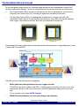
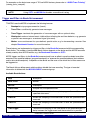
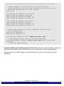
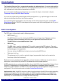
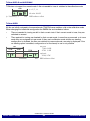
The Emulation Device Concept
For cost and power saving reasons, the trace and trigger features are only implemented in special SoC
versions, the Emulation Devices. The normal Product Devices for the mass-market do not contain them.
•
The Product Device (PD) is for the mass production but also for development. It consists of a
single die, the Product Chip (PC), including all application and debug functionality.
•
The Emulation Device (ED) is for development and field tests. It contains two dies, the
unmodified Product Chip (PC) and the Emulation Extension Chip (EEC) offering the additional
trace, trigger, and calibration features. Both dies are connected by bond wires.
PC
PC
Product Device
EEC
Emulation Device
The packages of Product and Emulation Devices almost have the same pinout. A single debug port is used
to access the PC and the EEC.
Product Chip
Processor Bus
IO32
CPU
C
2
CPU
C
PPUU
CPU
01
Bus
B
us01
Bus
DAP/
JTAG
Trace Signals
IO32
MCDS
PMU/
LMU
Debug Cable
EMEM
AGBT
Preprocessor
Back Bone Bus
Emulation Extension Chip
The EEC consists of the following main components:
•
MCDS (Multi-core Debug Solution) for trace, trigger and filter
The MCDS is the basic module of the EEC, it collects status information from the various chip
components. Based on the status information, the MCDS generates debug events and trace
data.
For an overview, see chapter MCDS Concept.
•
EMEM (Emulation Memory) for trace data storage and calibration
©1989-2015 Lauterbach GmbH
MCDS User’s Guide
9
Background Information
The Emulation Memory is a dual-ported memory used for storing the generated on- and off-chip
trace data as well as calibration information. On some devices, the EMEM can be used as
additional application RAM via the LMU.
The EMEM is discussed in chapter Emulation Memory.
•
AGBT (Aurora GigaBit Trace) for serial high-speed off-chip trace
The Aurora GigaBit Trace module uses the Aurora serial protocol to transfer the generated trace
data to the TRACE32 preprocessor. AGBT uses a part of the EMEM as FIFO.
The AGBT off-chip trace is discussed in chapter AGBT High-speed Serial Trace.
•
BBB (Back Bone Bus) for connecting the EEC modules
The BBB is an FPI bus independent from the Product Chip for connecting all EEC components,
memories, and registers. It can be accessed by the debugger via the debug port.
On TriCore the application can also access the BBB using the MLI bridge (TriCore AUDO) or the
LMU (TriCore AURIX). On XC2000 Emulation Devices the application cannot access the EEC
components.
•
Cerberus IO Client (IO32)
The Cerberus IO Client (IO32) on the EEC enables the TRACE32 debugger to configure the
Emulation Device and to read out the EMEM via the debug port of the Product Device.
•
Other peripherals
Depending on the device, the EEC may provide additional peripheral components. They are
mainly used for a specific purpose only, e.g. USB over Emulation Device or the Camera Interface
(CIF), and are not covered by this document.
Older TriCore devices up to AUDO-NG feature an OCDS-L2 off-chip trace port (parallel trace) to provide
information about the program flow via a dedicated protocol. This obsolete trace protocol was part of the
Product Chip and is not related to the Emulation Device or MCDS.
©1989-2015 Lauterbach GmbH
MCDS User’s Guide
10
Background Information
TRACE32 Support for Emulation Devices
This chapter describes how TRACE32 supports the various Emulation Device features, the required
licenses, and the physical device connection. All MCDS users are advised to read this chapter.
The MCDS command group is used for configuring the MCDS, the AGBT, and the Emulation Memory.
Feature Overview
When trace is available, TRACE32 provides an out-of-the box trace configuration: the program flow trace for
the first core of the architecture is selected by default. As soon as program execution starts, recording is
started, too.
NOTE:
The MCDS of TriCore devices is restricted to generate trace and trigger
information only for up to two cores, even if the devices have more cores.
If the device supports off-chip trace and a suitable trace preprocessor is connected, off-chip trace is used is
used automatically (Trace.METHOD Analyzer). Otherwise on-chip trace is configured automatically
(Trace.METHOD Onchip).
The most important and most frequently-used features can easily be selected and configured with the
following commands:
MCDS.state
Opens the MCDS.state window, where you can quickly enable and disable
the different trace sources.
Break.Set
Allows you to easily configure commonly used trace triggers and filters,
including OS-aware tracing (option /TraceData).
CTS
CTS (Context Tracking System) allows debugging an application based on
its program trace recording.
BMC
Benchmark Counters are used to count important events, e.g. cache hits and
misses, the number of calls to a function or exceptions.
OCTL
Specific trigger and filter setups can be programmed using OCTL. MCDS
Expert users can get low level access to the MCDS as explained in chapter
Guarded MCDS Programming.
Target Interface
No extra debug port is required for accessing and configuring the EEC. Only one debug cable is required for
debug and on-chip trace.
©1989-2015 Lauterbach GmbH
MCDS User’s Guide
11
TRACE32 Support for Emulation Devices
The debug port connector, the debug cables and available adapters and converters are described in the
following application notes:
•
“Application Note Debug Cable TriCore” (tricore_app_ocds.pdf)
•
“Application Note Debug Cable C166” (c166_app_ocds.pdf)
For the AGBT off-chip trace, the 22-pin ERF-8 trace connector is required. The trace connector also includes
the debug signals, so the debug cable and the trace preprocessor can be connected to the target via one
connector. For the pinout and the signals, refer to:
•
http://www.lauterbach.com/ad3829.html
•
“ERF8 22-pin Power.org Connector” (debugger_tricore.pdf)
•
Infineon Application Note AP32186 “Aurora Connector & Cable”
Lauterbach uses the Infineon TriBoards for development and verification. Their documentation contains
schematics and additional information about the debug and trace interfaces. Lauterbach recommends
that you use this information as reference for proprietary hardware.
In addition to the break pins at the debug port, most TriCore Emulation Devices have further package pins to
provide an external trigger signal. These pins are often also available via the GPIO ports. For more
information, see the Infineon User’s Manual and Data Sheet of your device.
MCDS Licensing
The use of the MCDS trigger features and the EEC access is covered by the architecture’s debug license.
Decoding the MCDS trace data requires an extra license:
•
TriCore-MCDS for TriCore, including PCP and GTM.
•
C166-MCDS for XC2000ED and C166.
The trace license is either stored in the debug cable or in the trace preprocessor and can be used for on- and
off-chip trace. For example, the TriCore-MCDS license stored in the preprocessor connected to the trace
module can be used for TriCore MCDS on-chip trace.
NOTE:
•
•
The Serial Trace preprocessor is architecture independent. In case originally purchased for PowerPC or ARM it does not contain an MCDS
license.
The obsolete OCDS-L2 preprocessor (parallel trace) is not recognized as
an MCDS trace license as the trace protocols are completely different.
©1989-2015 Lauterbach GmbH
MCDS User’s Guide
12
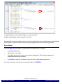
TRACE32 Support for Emulation Devices
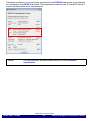
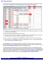
The licenses available for your current setup are displayed in the VERSION.view window. A more detailed
list is displayed in the LICENSE.List window. The example below shows that the TriCore-MCDS license is
stored in the debug cable and in the preprocessor.
NOTE:
For order information and prices, please contact your local Lauterbach
representative.
©1989-2015 Lauterbach GmbH
MCDS User’s Guide
13
TRACE32 Support for Emulation Devices
MCDS Basic Features
This chapter introduces the basic features of the TRACE32 support for MCDS, especially the trigger and
filter configuration via the Break.Set command. All MCDS users using trace and trigger are strongly advised
to read this chapter.
MCDS Concept
The MCDS is the main module of the EEC, it collects status information of the various chip components.
Based on the collected status information, the MCDS generates debug and trace events as well as trace
data. Understanding the MCDS concept helps understanding its behavior.
The MCDS consists of one or more independent Observation Blocks receiving status and run-time
information from a core or bus. This information can be written to the trace buffer or used to generate debug
and trace signals:
•
Debug signals are used to generate signals to the SoC, e.g. to stop a core or to toggle a pin.
•
Trace signals together with optional trace filters are used to enable or disable trace data
generation, to generate a watchpoint message, or to count events.
-
For information about watchpoint messages, see chapter Watchpoints.
-
For information about event counters, see chapter Benchmark Counters.
The basic MCDS setup is identical for on- and off-chip trace.
MCDS of XC2000ED and C166
XC2000 and C166 Emulation Devices only have one observation block. Only the core can be observed.
©1989-2015 Lauterbach GmbH
MCDS User’s Guide
14
MCDS Basic Features
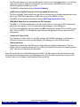
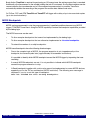
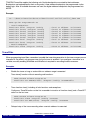
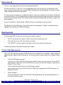
MCDS of TriCore
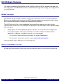
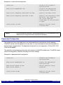
TriCore has up to two Processor Observation Blocks (POB) to observe the cores (TriCore, PCP and GTM)
and two Bus Observation Blocks (BOB)) to observe the buses (LMB, SRI, SPB or RPB).
Product Chip
CPU
C
2
CPU
C
PPUU
CPU
01
POBY
POBY
POBx
MCDS
Bus
B
us01
Bus
MCX
BOBY
BOBY
BOBx
MEM IF
Emulation Extension Chip
The trace data generated by the Observation Blocks is forwarded to the Memory Interface (MEM IF) where
all messages are sorted according their temporal order and then written to the Emulation Memory.
©1989-2015 Lauterbach GmbH
MCDS User’s Guide
15
MCDS Basic Features
The POBs observe the program execution as well as the data accesses of the core (program- and data
trace). The BOBs observe the data transactions on the buses (data trace), also containing meta information
about the transaction, e.g. bus master, channel and priority.
NOTE:
Restrictions for TriCore AUDO-NG:
•
LMB cannot be traced.
Restrictions for TriCore AURIX:
•
Only two out of four cores can be selected for trace and trigger.
•
HSM cannot be traced, all related bus traffic is removed on SoC level.
•
SCR cannot be traced, all related bus accesses available.
The Multi-core Cross-connect (MCX) does not observe anything. It is used for generating the timestamp
messages and contains counters.
•
The counters can be used to count internal evens (see chapter Benchmark Counters).
Alternatively counters can be used to implement state machines. This allows to implement trace
filters, e.g. record all bus transactions while a specific function is active.
•
MCDS does not attach timestamp information to each trace message. Instead, the timestamps
are dedicated messages. So several messages generated at the same time share one
timestamp message to reduce trace buffer consumption.
•
Timestamps can be enabled continuously or on demand to tag dedicated events only. The
Observation Blocks can signal the MCX to generate a timestamp in case an event happened.
NOTE:
For TriCore AUDO this signal from the Observation Block to the MCX is
delayed, so the timestamp messages are generated asynchronously, resulting
in incorrect timestamp information. To avoid this, TRACE32 only allows
continuous timestamp generation for TriCore AUDO. For TriCore AURIX this
issue is fixed. See chapter No Trace Content Displayed for more information.
MCDS Configuration
The MCDS command group is used to configure the MCDS. For a complete description of all MCDS
commands, see chapter “MCDS” in General Commands Reference Guide M, page 57
(general_ref_m.pdf).
The MCDS.state window shows the most important configuration options available for the selected device.
The following sections give an overview and introduction only, please refer to the corresponding chapters of
this User’s Guide to get more information.
©1989-2015 Lauterbach GmbH
MCDS User’s Guide
16
MCDS Basic Features
General Settings
General MCDS configuration:
•
The TRACE32 MCDS implementation has two states: ON and OFF.
The default is MCDS.ON. It is required for tracing and programming any triggers and filters. If
switched off (MCDS.OFF), TRACE32 does not access any MCDS register. This can be used to
avoid interference with third-party tools or applications.
•
MCDS.RESet resets all MCDS configuration to the default.
•
MCDS.CLEAR deletes all configuration made by the MCDS.Set command group. See chapter
Guarded MCDS Programming for details.
•
MCDS.INFO provides information about the availability of hardware resources.
•
MCDS.Register opens a peripheral access to all MCDS registers.
Buttons as shortcuts to MCDS related features:
•
CLOCK: SoC clock configuration, required for using timestamps.
•
BMC: Count MCDS generated events using the Benchmark Counters.
•
Trace: Configure the currently selected Trace method.
Timestamp Setup
Enabling and using the MCDS-generated on-chip timestamps requires two steps:
•
Enable the MCDS timestamp generation: MCDS.TimeStamp ON.
•
Use the CLOCK commands to inform TRACE32 about the chip’s base clocks. CLOCK.ON tells
TRACE32 to use these clocks for calculating the timestamps.
©1989-2015 Lauterbach GmbH
MCDS User’s Guide
17
MCDS Basic Features
Example:
SYStem.CPU TC275TE
CLOCK.OSCillator 20.0MHz
CLOCK.ON
; frequency of on-board
oscillator
SYStem.Mode Up
Data.LOAD.Elf myapplication.elf /NoCODE
Go PLL_ConfigDone
CLOCK.view
; manually verify clock setup
MCDS.TimeStamp ON
; enable timestamp generation
NOTE:
A correct programming of the on-chip clocks is mandatory for a correct operation of
the MCDS hardware and timestamp generation. See chapter EEC Clock System
for details.
Timestamp decoding requires the entire trace buffer to be processed. For huge trace buffers, e.g. off-chip
trace, this may take up to several minutes.
Trace Buffer Configuration
TRACE32 can be configured to share the EMEM with third-party tools or applications using the
MCDS.TraceBuffer commands. See chapter Emulation Memory for details.
As long as no sharing of the EMEM is required TRACE32 automatically chooses the most suitable EMEM
configuration.
NOTE:
XC2000 Emulation Devices do not allow configuring the EMEM.
AGBT Off-chip Trace Configuration
The commands MCDS.PortSIZE and MCDS.PortSPEED are used to configure the Aurora GigaBit Trace
(AGBT). See chapter AGBT High-speed Serial Trace for more information.
Trace Sources
Selecting a trace source enables the generation of the corresponding trace data. On TriCore, the trace
sources of the different cores and buses can be enabled independently. On XC2000 only the core can be
traced.
For the program trace different variants exist: program trace, sync trace, and CFT. For details please refer to
chapter Trace Sources.
©1989-2015 Lauterbach GmbH
MCDS User’s Guide
18
MCDS Basic Features
TriCore AURIX is limited to tracing only two cores at the same time. Multiplexers are implemented to select
the cores to be traced. Use the command MCDS.SOURCE.Set CpuMux[0 | 1].Core to configure them.
The TriCore SRI is not a bus, it is a fabric that can perform more than one transaction per clock cycle. The
MCDS hardware is limited to tracing only two transactions in parallel. The command MCDS.SOURCE.Set
SRI.[1 | 2].SLAVE is used to select the corresponding bus slave. All transactions to selected slaves are
recorded. The masters that initiated these transactions are available from the recorded trace data.
The GTM peripheral module is implemented as a peripheral trace. So in addition to the executed instructions
and data accesses internal signals can be recorded, too. These signals can be displayed as a timing
diagram, implementing the feature of an on-chip logic analyzer. See “GTM Debugger and Trace”
(debugger_gtm.pdf) and the TriCore-related GTM demos in demo/gtm/hardware/ for more information.
NOTE:
OCTL and MCDS.Set have their own methods for selecting the trace sources.
Example: Core Trace on TriCore AURIX
1.
On TriCore TC277TE, the program flow of core 0 and core 1 are to be traced. Additionally all read
accesses of core 0 and all write accesses of core 1 are to be recorded:
MCDS.SOURCE.RESet
; configure trace for core 0
MCDS.SOURCE.CpuMux0.Core TriCore0
MCDS.SOURCE.CpuMux0.Program ON
MCDS.SOURCE.CpuMux0.PTMode FlowTrace
MCDS.SOURCE.CpuMux0.ReadAddr ON
; read data trace not implemented by MCDS
; configure trace for core 1
MCDS.SOURCE.CpuMux1.Core TriCore1
MCDS.SOURCE.CpuMux1.Program ON
MCDS.SOURCE.CpuMux1.PTMode FlowTrace
MCDS.SOURCE.CpuMux1.WriteAddr ON
MCDS.SOURCE.CpuMux1.WriteData ON
2.
On TriCore TC277TE, the program flow of core 1 and the performed read and write accesses are
to be traced. The sync trace is to be used to show the correct temporal order of the executed
instructions and performed accesses:
MCDS.SOURCE.RESet
; configure trace for core 0
MCDS.SOURCE.CpuMux0.Core TriCore1
MCDS.SOURCE.CpuMux0.Program ON
MCDS.SOURCE.CpuMux0.PTMode SyncTrace
MCDS.SOURCE.CpuMux0.ReadAddr ON
MCDS.SOURCE.CpuMux0.WriteAddr ON
MCDS.SOURCE.CpuMux0.WriteData ON
©1989-2015 Lauterbach GmbH
MCDS User’s Guide
19
MCDS Basic Features
Example: Bus Trace on TriCore AUDO-MAX
1.
On TriCore TC1798ED, all read accesses to PMU0 (internal Flash) and all write accesses to the
EBU area to be traced:
MCDS.SOURCE.RESet
MCDS.SOURCE.NONE ; disable all trace sources
; trace all read accesses to PMU0
MCDS.SOURCE.SRI.1.SLAVE PMU0
MCDS.SOURCE.SRI.1.ReadAddr ON
MCDS.SOURCE.SRI.1.ReadData ON
; trace all write accesses to the EBU
MCDS.SOURCE.SRI.2.SLAVE EBU
MCDS.SOURCE.SRI.2.WriteAddr ON
MCDS.SOURCE.SRI.2.WriteData ON
2.
On TriCore TC1798ED, all accessed peripherals are to be traced:
MCDS.SOURCE.RESet
MCDS.SOURCE.NONE ; disable all trace sources
; trace all accessed peripherals
MCDS.SOURCE.SPB.ReadAddr ON
MCDS.SOURCE.SPB.WriteAddr ON
©1989-2015 Lauterbach GmbH
MCDS User’s Guide
20
MCDS Basic Features
Trace Control
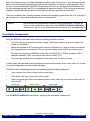
TRACE32 provides two different methods for controlling the MCDS trace:
•
The Analyzer commands are used to control the off-chip trace [A].
•
The Onchip commands are used to control the on-chip trace [B].
A
B
MCDS allows only one of these trace methods to be active at the same time. Unless stated otherwise the
commands described here can be applied to Analyzer as well as to Onchip.
In this chapter:
•
Trace state and mode
•
Trace buffer size and usage
•
TraceTrigger configuration
Here, only the most important commands are described. For more information about these commands as
well as those not mentioned here, please refer to the command group Trace.
Trace States
The DISable state prevents tracing at all. The EMEM is not configured so it can be used exclusively for
another purpose, e.g. calibration. Refer to chapter Emulation Memory for more information. Using the
MCDS for triggering is possible in this state, any trace data generated by the chip will be ignored.
The default trace state is OFF, which means that TRACE32 configures the necessary parts of the EMEM for
tracing. Note that in the OFF state no trace data is recorded.
The EMEM is ready to capture trace data in the Arm state. Any generated trace data will be recorded.
©1989-2015 Lauterbach GmbH
MCDS User’s Guide
21
MCDS Basic Features
The TRIGGER and break states are related to the TraceTrigger option. TRIGGER means that the
configured event has occurred but the trace is still recording (transition from Arm to TRIGGER). When
recording has stopped, the trace switches to the break state to indicate that recording has stopped due to
the occurrence of the configured trigger. The delay between TRIGGER and break can be configured with
Trace.TDelay.
NOTE:
Trace.TDelay is only available for Onchip.
Trace Buffer Size and Usage
The SIZE box shows how many bytes of the trace memory are used as trace buffer:
•
Trace method Analyzer
Trace buffer size of the Power Trace module.
•
Trace method Onchip
Size of the EMEM used for tracing. Refer to chapter Emulation Memory for more information and
for changing the EMEM usage for trace and calibration.
The progress bar under used indicates the fill state of the trace buffer. The fill rate depends on the amount of
generated trace data and the configured clocks.
The trace buffer will normally not be filled completely with trace data. The reason is that the
decompression information is located at the beginning of a paragraph (usually 1 or 4 KB). Refer to
chapter EMEM Partitioning for details on the trace buffer organization.
Trace Modes
The trace memory can be operated in different modes, see Trace.Mode for details.
•
In Fifo mode the trace recording is endless. Use this mode when you are interested in the data
up to the point where trace recording is stopped.
•
In Stack mode recording is stopped when the trace buffer is full while program execution
continues. This mode is useful when the information of interest is assumed close to the start of
the recording and program execution must not be stopped.
•
The Leash mode is similar to the Stack mode with the difference that program execution is
stopped when the trace buffer is full. This mode can be used to generate a seamless trace by
joining smaller trace recordings to a large one. For more information, see the Trace.JOINFILE
command. Leash mode is not supported by all Emulation Devices.
Trace Trigger Configuration
A TraceTrigger can be used to capture run-time information of what happened before and after an event.
This means that program execution must not be stopped, instead trace recording continues for some time
after the event. Using the TraceTrigger option in TRACE32 you can trigger on the event of interest, and with
the Trace.TDelay feature you can define which amount of the trace buffer is reserved for the trace data
generated after the event.
©1989-2015 Lauterbach GmbH
MCDS User’s Guide
22
MCDS Basic Features
Programming the TraceTrigger event is performed via the TraceTrigger action of Break.Set, see chapter
Trace Trigger for an example.
NOTE:
The TraceTrigger feature normally only makes sense in Fifo mode. It is not
available in Stack mode, configuration is silently ignored.
Other Trace Configuration Commands
•
Trace.RESet resets all settings of the Trace command group to the defaults, the trace buffer is
initialized. Only the selected trace method is reset.
•
Trace.Init initializes the trace buffer by discarding all recorded data.
NOTE:
The on-chip trace buffer is always cleared when a new trace recording is started. It
is not possible to attach a new recording to the previous one. Instead, save the
recording to a file, and attach the recording to the contents of the file using
Trace.JOINFILE.
•
Trace.AutoArm will start and stop the trace recording simultaneously with the program
execution. Resuming program execution will automatically start trace recording (Arm state), a
break terminates trace recording (OFF state).
•
Trace.AutoInit will initialize the trace buffer and discard all recorded data when resuming
program execution.
Basic Trace Usage
The default MCDS setup allows the user to perform unconditional tracing without additional configuration:
•
The first core of the device is configured to generate trace data for the program flow. Data trace,
bus trace and timestamps are disabled.
•
Trace recording automatically starts when the core starts execution and stops when the core
breaks. See command Trace.AutoArm for details.
•
The EMEM is configured automatically depending on the device and the trace method. For onchip trace the maximum possible size is selected. Refer to chapter Emulation Memory if a
different configuration is required.
•
Endless recording is configured so the program flow up to the break can be inspected. For
details, see command Trace.Mode Fifo.
©1989-2015 Lauterbach GmbH
MCDS User’s Guide
23
MCDS Basic Features
For examples on the basic trace usage of TriCore AURIX devices, please refer to “AURIX Trace Training”
(training_aurix_trace.pdf).
NOTE:
Using OCTL and MCDS.Set disables unconditional tracing.
Trigger and Filter via Break.Set command
TRACE32 uses the MCDS to implement the following features:
•
Breakpoint: stop program execution (break).
•
Trace Filter: conditionally generate trace messages.
•
Trace Trigger: terminate the generation of trace messages with an optional delay.
•
Watchpoint: make an internal event visible without affecting the real-time behavior, e.g. generate
a special trace message or an external signal (pin event).
•
Marker: use a certain event for a pre-defined, special action, e.g. for incrementing a counter. See
chapter Benchmark Counter for more information.
These features are implemented as trigger and filter via the Break.Set command with the corresponding
Break Action. The number of configurable Break Actions depends on the device and the MCDS resources
already used by other MCDS features, e.g. the Benchmark Counters or OCTL.
MCDS triggers and filters via the Break.Set command only have an effect in case the related core either
executes at the specified address (program breakpoint) or accesses the specified address (data address
and/or data value breakpoint). It depends on the device and the core or bus which kind of data access can
be triggered on.
The Break Actions define events which enable or disable the trace recording. The type of recorded
information is defined with the MCDS.SOURCE command group.
Available Break Actions:
stop
Breakpoint
Delta, Echo
Marker
WATCH
Watchpoint
TraceEnable
Sample only the specified event.
TraceData
OS-aware trace: sample the complete program flow and the
specified data event.
TraceON
Switch the sampling to the trace buffer on after the specified event
occurred.
TraceOFF
Switch the sampling to the trace buffer off after the specified event
occurred.
TraceTrigger
Terminate the sampling to the trace buffer at the specified event. A
delay between the trigger event and the termination is possible.
©1989-2015 Lauterbach GmbH
MCDS User’s Guide
24
MCDS Basic Features
Break Action TraceData is required for performing an OS-aware trace: the entire program flow is recorded.
Additionally all write accesses to the variable holding the task ID are traced. So all context switches can be
reconstructed by the trace decoder and a OS-aware performance analysis is possible. Trace Data
automatically enables the recording of the program flow and the data address and value.
On TriCore, PCP and GTM TraceON and TraceOFF will trigger with a delay of up to two core clock cycles
(up to six core instructions).
MCDS Breakpoints
MCDS can be programmed to stop the program execution if specified conditions become true (MCDS
trigger). TRACE32 PowerView is using this MCDS capability to extend the breakpoint capabilities provided
by the debug logic.
The MCDS resources can be used:
•
To allow complex breakpoints that cannot be implemented by the debug logic.
•
To allow complex breakpoints that are otherwise implemented as intrusive breakpoints.
•
To extend the number of on-chip breakpoints.
MCDS-based breakpoints have the following disadvantages:
•
Due to the complex logic of MCDS, the program execution is not stopped exactly at the
breakpoint, but several cycles later (approximately 20 assembler instructions).
It is possible to identify which MCDS breakpoint caused the MCDS trigger by inspecting the trace
recording.
•
If several MCDS breakpoints are set, it is not possible to indicate which MCDS breakpoint
caused the program execution to stop.
•
A Read breakpoint together with a data value cannot be implemented on some MCDS devices,
especially not for the TriCore architecture (MCDS restriction). The following error message is
displayed, if you try to set this type of breakpoint:
data not allowed for this on-chip breakpoint.
©1989-2015 Lauterbach GmbH
MCDS User’s Guide
25
MCDS Basic Features
If you want to use MCDS-based breakpoints, you have to enable the following MCDS resources:
MCDS.Option ProgramBreak ON
Allow TRACE32 PowerView to use MCDS to set Program
breakpoints.
MCDS.Option AddrBreak ON
Allow TRACE32 PowerView to use MCDS to set Read/Write/
ReadWrite breakpoints.
MCDS.Option AddrBreak ON
MCDS.Option DataBreak ON
TriCore: Allow TRACE32 PowerView to use MCDS to set
Write breakpoints when specified data values are written.
Others: Allow TRACE32 PowerView to use MCDS to set
Read/Write/ReadWrite breakpoints when specified data
values are written respectively to set Read breakpoints when
specified data values are read.
(if supported by MCDS)
Complex Breakpoints
TRACE32 PowerView allows to configure a breakpoint that stops the program execution if an instruction of a
specified instruction range accesses a specified data range.
©1989-2015 Lauterbach GmbH
MCDS User’s Guide
26
MCDS Basic Features
Example 1 (single-core): Stop the program execution if an instruction of the function sieve() writes 0x0 to
the variable flags[3].
DO ~~\demo\tricore\hardware\triboard-tc2x5\tc275tf\tc275tf_demo.cmm
; configure MCDS to generate trace information for the instruction
; execution sequence and all write accesses
MCDS.state
MCDS.SOURCE.Set CpuMux0.Program ON
MCDS.SOURCE.Set CpuMux0.WriteAddr ON
MCDS.SOURCE.Set CpuMux0.WriteData ON
; enable MCDS breakpoints on program addresses, data addresses
; and data values
MCDS.Option ProgramBreak ON
MCDS.Option AddrBreak ON
MCDS.Option DataBreak ON
Var.Break.Set sieve /VarWrite flags[3] /DATA.Byte 0x0
; start program execution and wait until it stops at the breakpoint
Go
WAIT !STATE.RUN()
; find the MCDS trigger event in the trace recording
Trace.Find Address Var.RANGE(flags[3]) Data.B 0x0 CYcle Write /Back
IF FOUND()
Trace.List TRACK.RECORD()
Example 2 (single-core): Stop the program execution if an instruction outside of the function func10()
writes 0x0 to the variable flags[3].
©1989-2015 Lauterbach GmbH
MCDS User’s Guide
27
MCDS Basic Features
DO ~~\demo\tricore\hardware\triboard-tc2x5\tc275tf\tc275tf_demo.cmm
; configure MCDS to generate trace information for the instruction
; execution sequence and all write accesses
MCDS.state
MCDS.SOURCE.Set CpuMux0.Program ON
MCDS.SOURCE.Set CpuMux0.WriteAddr ON
MCDS.SOURCE.Set CpuMux0.WriteData ON
; enable MCDS breakpoints on program addresses, data addresses
; and data values
MCDS.Option ProgramBreak ON
MCDS.Option AddrBreak ON
MCDS.Option DataBreak ON
Var.Break.Set func10 /VarWrite flags[3] /DATA.Byte 0x0 /EXclude
; start program execution and wait until it stops at the breakpoint
Go
WAIT !STATE.RUN()
; find the MCDS trigger event in the trace recording
Trace.Find Address Var.RANGE(flags[3]) Data.B 0x0 CYcle Write /Back
IF FOUND()
Trace.List TRACK.RECORD()
Example 3 (SMP system consisting of three TriCore cores): Stop the program execution if an instruction
of the function sieve() writes 0x0 to the variable flags[3].
Please be aware that MCDS-based breakpoints can only be programmed to cores that are connected to the
trace multiplexer.
©1989-2015 Lauterbach GmbH
MCDS User’s Guide
28
MCDS Basic Features
DO ~~\demo\tricore\hardware\triboard-tc2x5\tc275tf\tc275tf_smp_demo_multisieve.cmm
; connect TriCore0 and TriCore1 to the trace multiplexer
; configure MCDS to generate trace information for the instruction
; execution sequence and all write accesses
MCDS.state
MCDS.SOURCE.Set
MCDS.SOURCE.Set
MCDS.SOURCE.Set
MCDS.SOURCE.Set
CpuMux0.Core TriCore0
CpuMux0.Program ON
CpuMux0.WriteAddr ON
CpuMux0.WriteData ON
MCDS.SOURCE.Set
MCDS.SOURCE.Set
MCDS.SOURCE.Set
MCDS.SOURCE.Set
CpuMux1.Core TriCore1
CpuMux1.Program ON
CpuMux1.WriteAddr ON
CpuMux1.WriteData ON
; enable MCDS breakpoints on program addresses, data addresses
; and data values
MCDS.Option ProgramBreak ON
MCDS.Option AddrBreak ON
MCDS.Option DataBreak ON
Var.Break.Set sieve /VarWrite flags[3] /DATA.Byte 0x0
; start program execution and wait until it stops at the breakpoint
Go
WAIT !STATE.RUN()
; Find the MCDS trigger event in the trace recording
Trace.Find Address Var.RANGE(flags[3]) Data.B 0x0 CYcle Write /Back
IF FOUND()
Trace.List TRACK.RECORD()
Real-time MCDS Breakpoints Instead of Intrusive Breakpoints
The debug-logic of the TriCore does not provide data value breakpoints. The following breakpoint is
implemented as an intrusive breakpoint by default.
Var.Break.Set flags[12] /Write /DATA.Byte 0x0
The following commands allow TRACE32 PowerView to implement this type of breakpoint as a real-time
MCDS breakpoint. Please be aware that this is only possible for Write breakpoints.
MCDS.Option AddrBreak ON
MCDS.Option DataBreak ON
Allow TRACE32 PowerView to use MCDS to set Write
breakpoints when specified data values are written.
(TriCore)
©1989-2015 Lauterbach GmbH
MCDS User’s Guide
29
MCDS Basic Features
Example 1 (single-core): Stop the program execution if 0x0 as a byte is written to the variable flags[12].
DO ~~\demo\tricore\hardware\triboard-tc2x5\tc275tf\tc275tf_demo.cmm
; configure MCDS to generate trace information for the instruction
; execution sequence and all write accesses
MCDS.state
MCDS.SOURCE.Set CpuMux0.Program ON
MCDS.SOURCE.Set CpuMux0.WriteAddr ON
MCDS.SOURCE.Set CpuMux0.WriteData ON
; enable MCDS breakpoints on data addresses and data values
; (write access only)
MCDS.Option AddrBreak ON
MCDS.Option DataBreak ON
Var.Break.Set flags[12] /Write /DATA.Byte 0x0
; start program execution and wait until it stops at the breakpoint
Go
WAIT !STATE.RUN()
; find the MCDS trigger event in the trace recording
Trace.Find Address Var.RANGE(flags[12]) Data.B 0x0 CYcle Write /Back
IF FOUND()
Trace.List TRACK.RECORD()
Example 2 (single-core): Stop the program execution if a data value other than 0x0 is written as a byte to
the variable flags[12].
©1989-2015 Lauterbach GmbH
MCDS User’s Guide
30
MCDS Basic Features
DO ~~\demo\tricore\hardware\triboard-tc2x5\tc275tf\tc275tf_demo.cmm
; configure MCDS to generate trace information for the instruction
; execution sequence and all write accesses
MCDS.state
MCDS.SOURCE.Set CpuMux0.Program ON
MCDS.SOURCE.Set CpuMux0.WriteAddr ON
MCDS.SOURCE.Set CpuMux0.WriteData ON
; enable MCDS breakpoints on data addresses and data values
; (write access only)
MCDS.Option AddrBreak ON
MCDS.Option DataBreak ON
Var.Break.Set flags[12] /Write /DATA.Byte !0x0
; start program execution and wait until it stops at the breakpoint
Go
WAIT !STATE.RUN()
; find the MCDS trigger event is the trace recording
Trace.Find Address Var.RANGE(flags[12]) Data.B !0x0 CYcle Write /Back
IF FOUND()
Trace.List TRACK.RECORD()
Example 3 (SMP system consisting of three TriCore cores): Stop the program execution if 0x0 is written
as a byte to the variable flags[12].
Please be aware that a MCDS trigger can only be activated by a core that is connected to the trace
multiplexer.
©1989-2015 Lauterbach GmbH
MCDS User’s Guide
31
MCDS Basic Features
DO ~~\demo\tricore\hardware\triboard-tc2x5\tc275tf\tc275tf_smp_demo_multisieve.cmm
; connect TriCore0 and TriCore1 to the trace multiplexer
; configure MCDS to generate trace information for the instruction
; execution sequence and all write accesses
MCDS.state
MCDS.SOURCE.Set
MCDS.SOURCE.Set
MCDS.SOURCE.Set
MCDS.SOURCE.Set
CpuMux0.Core TriCore0
CpuMux0.Program ON
CpuMux0.WriteAddr ON
CpuMux0.WriteData ON
MCDS.SOURCE.Set
MCDS.SOURCE.Set
MCDS.SOURCE.Set
MCDS.SOURCE.Set
CpuMux1.Core TriCore1
CpuMux1.Program ON
CpuMux1.WriteAddr ON
CpuMux1.WriteData ON
; enable MCDS breakpoints on data addresses and data values
; (write access only)
MCDS.Option AddrBreak ON
MCDS.Option DataBreak ON
Var.Break.Set flags[12] /Write /DATA.Byte 0x0
; start program execution and wait until it stops at the breakpoint
Go
WAIT !STATE.RUN()
; find the MCDS trigger event is the trace recording
Trace.Find Address Var.RANGE(flags[12]) Data.B 0x0 CYcle Write /Back
IF FOUND()
Trace.List TRACK.RECORD()
Example 4 (SMP system consisting of three TriCore cores): Stop the program execution if a data value
between 0x10--0x20 is written as a long (32-bit) to the variable nAbsSmall.
Please be aware that a MCDS trigger can only be activated by a core that is connected to the trace
multiplexer.
©1989-2015 Lauterbach GmbH
MCDS User’s Guide
32
MCDS Basic Features
DO ~~\demo\tricore\hardware\triboard-tc2x5\tc275tf\tc275tf_smp_demo_waveform.cmm
; connect TriCore0 and TriCore1 to the trace multiplexer
; configure MCDS to generate trace information for the instruction
; execution sequence and all write accesses
MCDS.state
MCDS.SOURCE.Set
MCDS.SOURCE.Set
MCDS.SOURCE.Set
MCDS.SOURCE.Set
CpuMux0.Core TriCore0
CpuMux0.Program ON
CpuMux0.WriteAddr ON
CpuMux0.WriteData ON
MCDS.SOURCE.Set
MCDS.SOURCE.Set
MCDS.SOURCE.Set
MCDS.SOURCE.Set
CpuMux1.Core TriCore1
CpuMux1.Program O
CpuMux1.WriteAddr ON
CpuMux1.WriteData ON
; enable MCDS breakpoints on data addresses and data values
; (write access only)
MCDS.Option AddrBreak ON
MCDS.Option DataBreak ON
Var.Break.Set nAbsSmall /Write /DATA.Long 0x10..0x20
; find the MCDS trigger event is the trace recording
Trace.Find Address nAbsSmall Data.L 0x10--0x20 CYcle Write /Back
IF FOUND()
Trace.List TRACK.RECORD()
Example 5 (SMP system consisting of three TriCore cores): Stop the program execution if a data value
between less than 0x10 or greater than 0x20 is written as a long (32-bit) to the variable nAbsSmall.
Please be aware that a MCDS trigger can only be activated by a core that is connected to the trace
multiplexer.
©1989-2015 Lauterbach GmbH
MCDS User’s Guide
33
MCDS Basic Features
DO ~~\demo\tricore\hardware\triboard-tc2x5\tc275tf\tc275tf_smp_demo_waveform.cmm
; connect TriCore0 and TriCore1 to the trace multiplexer
; configure MCDS to generate trace information for the instruction
; execution sequence and all write accesses
MCDS.state
MCDS.SOURCE.Set
MCDS.SOURCE.Set
MCDS.SOURCE.Set
MCDS.SOURCE.Set
CpuMux0.Core TriCore0
CpuMux0.Program ON
CpuMux0.WriteAddr ON
CpuMux0.WriteData ON
MCDS.SOURCE.Set
MCDS.SOURCE.Set
MCDS.SOURCE.Set
MCDS.SOURCE.Set
CpuMux1.Core TriCore1
CpuMux1.Program ON
CpuMux1.WriteAddr ON
CpuMux1.WriteData ON
; enable MCDS breakpoints on data addresses and data values
; (write access only)
MCDS.Option AddrBreak ON
MCDS.Option DataBreak ON
Var.Break.Set nAbsSmall /Write /DATA.Long !0x10..0x20
; find the MCDS trigger event is the trace recording
Trace.Find Address nAbsSmall Data.L 0x0--0x0f OR Data.L 0x21--0xffffffff
CYcle Write /Back
IF FOUND()
Trace.List TRACK.RECORD()
More On-chip (MCDS) Breakpoints
The number of Onchip Breakpoints provided by the debug logic is limited.
For details refer to chapter “On-chip Breakpoints” in TriCore Debugger and Trace, page 21
(debugger_tricore.pdf).
If more than the available number of Onchip breakpoints is set, the following error message is displayed:
no on-chip breakpoint of this type possible.
The following commands can be used to extend the number of Onchip breakpoints:
MCDS.Option ProgramBreak ON
Allow TRACE32 PowerView to use MCDS to set Program
breakpoints.
MCDS.Option AddrBreak ON
Allow TRACE32 PowerView to use MCDS to set Read/Write/
ReadWrite breakpoints.
©1989-2015 Lauterbach GmbH
MCDS User’s Guide
34
MCDS Basic Features
TRACE32 PowerView applies the following rule: Onchip breakpoints are sorted by their addresses.
Breakpoints are implemented by their sorting order. Lower address breakpoints are programmed via the
debug logic. After all available resources are used, the higher address breakpoints are programmed into
MCDS.
Example:
DO ~~\demo\tricore\hardware\triboard-tc2x5\tc275tf\tc275tf_demo.cmm
MCDS.Option ProgramBreak ON
; OCDS breakpoints
Break.Set func1 /Program /Onchip
Break.Set func20 /Program /Onchip
Break.Set func26 /Program /Onchip
Break.Set func27 /Program /Onchip
Break.Set func2a /Program /Onchip
Break.Set func47 /Program /Onchip
Break.Set func7 /Program /Onchip
Break.Set func9 /Program /Onchip
; MCDS breakpoint
Break.Set sieve /Program /Onchip
;
;
;
;
;
;
;
;
func1 at address
func20 at address
func26 at address
func27 at address
func2a at address
func47 at address
func7 at address
func9 at address
; sieve at address
0x70100A10
0x70100C86
0x70100CA0
0x70100CA8
0x70100CD4
0x70100D90
0x70100E20
0x701010CC
0x701012E8
Trace Filter
When programming trace filters, remember to enable the trace data generation for the trace sources you are
interested in. By default, only program trace for the first core is enabled. If you configure a trace filter on a
variable, manually enabling WriteAddr and WriteData is required for recording the data accesses.
Examples
•
Enable the trace as long as code within an address range is executed
Trace sieve() function without recording sub-functions:
MCDS.SOURCE TriCore Program ON
Break.Set Var.RANGE(sieve) /Program /Onchip /TraceEnable
•
Trace function sieve() including all sub-functions and exceptions.
Configure a TraceON action on the first assembler instruction of function sieve() and a TraceOFF
action on the last one:
MCDS.SOURCE TriCore Program ON
Break.Set sieve /Program /Onchip /TraceON
Break.Set Var.END(sieve) /Program /Onchip /TraceOFF
•
Delayed stop of the trace recording when a certain address is executed.
©1989-2015 Lauterbach GmbH
MCDS User’s Guide
35
MCDS Basic Features
Reserve 10 % of the trace buffer for recording the program trace after function sieve() has been
exited the first time. Stop trace recording, but continue program execution:
MCDS.SOURCE TriCore Program ON
Break.Set Var.END(sieve) /Program /Onchip /TraceTrigger
Onchip.TDelay 10%
After the function sieve() is exited for the first time not more than the defined 10 % of the trace
buffer will be used for recording. There is no possibility to cancel or restart this process. See the
Onchip.TDelay command for details.
NOTE:
The AGBT off-chip trace does not support the Trace Trigger feature.
TraceTrigger only makes sense in Fifo mode:
•
In Stack mode, the trace will stop recording only when the trace buffer is full for the first time. The
Trace Trigger watchpoint is generated.
•
In Leash mode recording is disabled in any case when the trace buffer is full for the first time. The
Trace Trigger watchpoint is generated.
©1989-2015 Lauterbach GmbH
MCDS User’s Guide
36
MCDS Basic Features
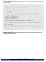
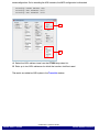
When programming Onchip.TDelay 0%, recording will be disabled, but the watchpoint message will be
missing in the trace.
F
B
D
C
G
H
A
E
A Breakpoint with action /TraceTrigger defines the trigger event.
B TDelay defines to continue recording after the trigger has occurred, using 10% of the total trace
buffer capacity for post-trigger recording.
C TRIGGER state indicates that the trigger has occurred and post-trigger recording is in progress.
D break state indicates that the trigger has occurred and post-trigger recording has completed.
E Status bar indicates that CPU is still executing (running), but post-trigger recording has completed.
F Size of data in trace buffer.
G A watchpoint TraceTrigger in the Trace.List window indicates the occurrence of the trigger.
H The watchpoint can be searched for using Trace.Find or Trace.FindAll. It is not possible to
distinguish the TraceTrigger watchpoint from any other watchpoint. See chapter Watchpoints for
details.
•
Trace all write accesses to a certain data address.
©1989-2015 Lauterbach GmbH
MCDS User’s Guide
37
MCDS Basic Features
All writes to the flags[3] variable are traced (data address and value):
MCDS.SOURCE.Set TriCore.Program OFF
MCDS.SOURCE.Set TriCore.WriteAddr ON
MCDS.SOURCE.Set TriCore.WriteData ON
Var.Break.Set flags[3] /Write /Onchip /TraceEnable
•
Trace all write accesses of a defined value to a data address.
Trace when 0x01 is written to the flags[3] variable. The code that triggered the access is also
traced:
MCDS.SOURCE.Set TriCore Program ON
; enable Program Flow Trace
MCDS.SOURCE.Set TriCore.WriteAddr ON
MCDS.SOURCE.Set TriCore.WriteData ON
Var.Break.Set flags[3] /Write /Data.Byte 0x01 /Onchip /TraceEnable
Note that the exact opcode triggering the data access may not be included in the trace, but the
recorded address specifies the location where to look for.
•
Trace all write accesses of a defined value to a data address triggered from a certain address
range.
In case the CPU executes within the function sieve(), all occurrences are traced where 0x01 is
written to the flags[3] variable. The code that triggered the access is also traced:
MCDS.SOURCE.Set TriCore.Program ON
MCDS.SOURCE.Set TriCore.WriteAddr ON
MCDS.SOURCE.Set TriCore.WriteData ON
Break.Set Var.RANGE(sieve) /MemoryWrite flags+0x0C \
/Data.Byte 0x01 /Onchip /TraceEnable
©1989-2015 Lauterbach GmbH
MCDS User’s Guide
38
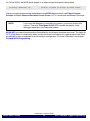
MCDS Basic Features
The TraceTrigger is marked in the trace as a special watchpoint [A] and can be searched in the trace listing
like a watchpoint. For more information, see chapter Watchpoints.
A
Watchpoints
TRACE32 can be programmed to generate a signal or a trace message in case a certain event has occurred
by using watchpoints. They are configured as breakpoints with break action WATCH.
©1989-2015 Lauterbach GmbH
MCDS User’s Guide
39
MCDS Basic Features
Example
Set a watchpoint on the entry of function sieve():
Break.Set sieve /Program /WATCH
The trace listing will show the name and the type of the watchpoint [A]:
A
NOTE:
The watchpoint message is independent of other messages, so it is not
possible to assign it to a certain program flow or data message.
NOTE:
Watchpoints will not generate messages on successive occurrences of an
event. The reason is that there must be an edge event (a transition from low to
high).
This is especially important when triggering on an address- or data value,
because the comparator will hold the last value until there is a new one. If the
address or value does not change on consecutive accesses, the comparator
value will not change and the watchpoint will miss the event.
Watchpoints can be searched, see chapter Searching the Trace.
©1989-2015 Lauterbach GmbH
MCDS User’s Guide
40
MCDS Basic Features
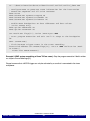
Trace Decoding
The recorded trace data can be displayed using the Trace.List command. TRACE32 reads the recorded
trace data from the trace buffer and starts decoding the trace data. When decoding is completed, the results
are shown in the Trace.List window as a continuous flow of the executed instructions.
D
F
A
G
B
C
E
A Executed assembler instructions.
B Executed HLL instructions and line numbers.
C Decoded trace information, e.g. reconstructed execution address and cycle type ptrace. The shown
trace listing is based on a flow trace, so ptrace information is only generated in case of a
discontinuity, e.g. branch, call, exception, …
D Record number. Negative numbers indicate cycles prior to the trace trigger, where the stop
recording event occurred.
E Optional timestamp information. Generated with every trace message. TIme.Back indicates the
time since the last trace message shown.
F Run information. Indicates linearity, discontinuity and the case: branch, call, return, exception.
G Symbol information related to the trace message’s address.
©1989-2015 Lauterbach GmbH
MCDS User’s Guide
41
MCDS Basic Features
NOTE:
•
•
TRACE32 will not read the trace buffer and start decoding until requested
by the user, e.g. by opening the Trace.List window.
Only the trace buffer required for displaying the results will be read and
decoded. When MCDS timestamps are enabled, the entire trace buffer is
decoded.
Depending on the recorded data and the device, TRACE32 tries to improve the decoding results:
•
Data Cycle Assignment
In case of an unconditional program flow trace, the trace decoder tries to assign the recorded
data accesses made by the core to their corresponding assembler instructions. Successfully
assigned data cycles are displayed in black, otherwise in red.
NOTE:
•
Bus cycles cannot be assigned to instructions.
Data Cycle Reordering (TriCore only)
In some cases the recorded data cycles will not appear in the order they were executed on the
device. If timestamps are available, the trace decoder is able to reconstruct the correct order.
Data Cycle Reordering is mandatory for Data Cycle Assignment.
The content shown in the Trace.List window can be defined. Each kind of trace information is represented
by a trace channel. Trace channels with related information are grouped, see the Trace.List command
description for details.
When no trace channel is specified, the DEFault trace channel group is displayed. For MCDS the following
trace channels are of interest:
•
BusMaster
Displays the originator (Bus Master) of a bus access. This information is only provided by MCDS
if the bus address trace has been enabled.
•
BusMODE
Displays whether the bus was accessed in User or Supervisor mode. This information is only
provided by MCDS if the bus address trace has been enabled. BusMaster and BusMODE
information are displayed in light grey if the access was made in User mode, otherwise in dark
grey.
•
TP
Displays the raw trace data. Only of interest for MCDS experts, e.g. for verifying the decoder.
•
MCDS
Displays the decoded message information, e.g. message source, trace type, and trace payload.
This information is useful for MCDS expert users having access to the Infineon ED
documentation. The message sources correspond to the MCDS unit names as defined by
Infineon.
©1989-2015 Lauterbach GmbH
MCDS User’s Guide
42
MCDS Basic Features
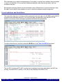
Bus Trace Information
As mentioned above the MCDS trace messages also provide information about the bus master. To obtain
this information, the generation of address messages has to be enabled for the related bus.
A
B
C
D
E
A Information about the originator of the bus access. May contain additional information, e.g. served
channel in case of DMA access.
B Information about the bus access mode: SV or user.
C Core data accesses (rd-data, wr-data) to CSA made by core 0. TriCore AURIX cannot trace read
data value. No bus information available, the originator is always the core.
D Core 1 performs data read access to D:0xF0000110 (peripheral). Data value cannot be traced.
E SPB read access to D:0xF0000110 made by bus master DMI of Core 1. This corresponds to data
access of D. Data value available (bus trace).
As the debugger is also a bus master and performs all accesses via the bus system, its accesses also
generate trace messages. The debugger by default suppresses the display of these messages. Using the
command Trace.Mode SLAVE ON these accesses will be displayed, too.
For DMA accesses MCDS generates information about the DMA controller or the Move Engine and the
related channel number. As only five bits are reserved for the channel information only 32 DMA channels are
supported. For TriCore devices with more DMA channels this information is ambiguous, so the DMA transfer
could have happened on channel 5, 37, 69, … For an unambiguous identification of the DMA channel the
Peripheral Trace has to be used. Refer to the example Peripheral Trace for DMA of TC277TE.
©1989-2015 Lauterbach GmbH
MCDS User’s Guide
43
MCDS Basic Features
Searching the Trace
You have the following options to search the trace data:
•
A text search within the Trace.List window
For a text search, press Ctrl+F. The text search ranges from the current trace record up to the first
occurrence of the search item.
The text search compares the content of the Trace.List window with the search item and will find any
occurrence. Because of the text comparison, the text search is very slow.
•
A command-based search
Events in the trace decoding can quickly be found using Trace.Find and Trace.FindAll. For a
general description, please refer to the descriptions of the commands. Only options of special
relevance for MCDS are described here.
•
For detailed information about the command based search, refer to “Application Note for the
Trace.Find Command” (app_trace_find.pdf).
Clicking the Find button in the Trace.List window will enable implicit tracking of the Trace.Find and
Trace.FindAll results with the Trace.List window. Otherwise tracking can be enabled with the Track option.
Specific Cycles
Read- and write accesses of a specific CPU are rare and hard to find, especially if a certain value is of
interest. In addition to the pre-defined cycle types, all cycle types listed in the cycle column of the Trace.List
window can be searched. The example shows a search for an SPB write access:
If necessary the search can be restricted to specific data values and access widths and types.
©1989-2015 Lauterbach GmbH
MCDS User’s Guide
44
MCDS Basic Features
Special Events
For MCDS, the following expert options are available for finding special events, depending on the device:
Events:
TRACEENABLE, WATCHPOINT, COUNTER
Exceptions:
EXCEPTION, INTERRUPT, TRAP, RESET
Error:
FIFOFULL, FLOWERROR
NOTE:
For watchpoints it is currently only possible to show the internal ID in the data
column but not the breakpoint configuration name. As watchpoints are
independent messages, it is also not possible to display the related symbol.
Exception Decoding
The MCDS flow trace protocol does not provide any information about entries into the exception handler so
displaying this event requires extra setup. For TriCore there are two methods available:
1.
Tables: They specify the locations of the exception handler
2.
DCU messages: They enable generation of extended trace data
©1989-2015 Lauterbach GmbH
MCDS User’s Guide
45
MCDS Basic Features
Exception Decoding Using Tables
For each TriCore core, one address range for an interrupt handler table and another one for a trap handler
table can be specified. By default, these tables are filled automatically by evaluating the BIV and BTV
registers of the cores before the trace decoding starts. For interrupts, it is assumed that all interrupts are
used.
In some cases, e.g. when BIV and BTV are destroyed or not all interrupts are used, it might be necessary to
specify the handler areas manually using the MCDS.Option eXception.TABLE command:
; 256 interrupt handler entries
MCDS.Option eXception.TABLE Interrupt 0xC0001000++0x2FFF
; 8 trap handler entries
MCDS.Option eXception.TABLE Trap 0xC0002000++0xFF
In the example above, the size of an exception handler entry is fixed to 32 bytes. In the example below, the
TriCore AURIX CPU uses a non-default entry size:
; 256 interrupt handler entries, 8 B entry size
MCDS.Option eXception.TABLE Interrupt 0x70001000++0x7FF 8.
; 8 trap handler entries, 32 B entry size
MCDS.Option eXception.TABLE Trap 0x70002000++0xFF
In case of multicore configurations, up to three address ranges can be specified, one for each core starting
with core 0.
The advantage of tables is that in case of a static exception configuration all exceptions are identified.
Additionally it is possible to distinguish between interrupts and traps.
If the exception configuration changes during run-time, only one exception configuration is valid. This is
either the automatically evaluated BIV and BTV configuration or the manually entered table configuration. As
BIV and BTV are normally only changed during the startup and configuration process where no interrupts
and traps occur the use of tables for exception decoding is the preferred solution.
For more information about disabling the tables completely or re-enabling automatic configuration, see
MCDS.Option eXception.
Exception Decoding Using DCU Messages
TriCore devices implementing TriCore v1.6 architecture or later (AUDO MAX, AURIX) have a flag
implemented in the debug messages (DCU messages) that indicates whether an exception is currently
active. When found in the trace data, this flag is evaluated and assigned to the corresponding program flow
message. With MCDS.Option eXception.DCU ON the unconditional generation of debug messages can
be enabled for all cores handled by the current GUI.
The advantage of DCU messages is that more exceptions can be identified in a dynamic system.
©1989-2015 Lauterbach GmbH
MCDS User’s Guide
46
MCDS Basic Features
DCU messages do not support nested exceptions. For example, a trap that occurs while an interrupt handler
is active is not identified. It is not possible to differentiate between traps and interrupts either, both are
marked as interrupts.
Both exception decoding methods can be combined to allow a differentiation of traps and interrupts using
the tables, and to identify more exceptions in case of a dynamic exception handler configuration.
Trace Limitations and Restrictions
The observation logic does not directly write the generated trace messages into the EMEM. Instead MCDS
processes these messages internally. If too many messages are generated, some internal FIFO will
overflow. In this case, an error message is generated and shown in the trace listing:
To display where the error occurred, include the MCDS item in the Trace.List DEFault command:
The first FIFO overflow is WTU_MCX, so one or more watchpoint messages generated by the MCX are
missing. The second FIFO overflow is TSU_MCX, here timestamp information is lost.
©1989-2015 Lauterbach GmbH
MCDS User’s Guide
47
MCDS Basic Features
MCDS Unlocking
This chapter describes how TRACE32 handles access to a device where MCDS is protected against
unauthorized access. Such a system cannot be traced or used for triggering unless the correct key for
unlocking is provided.
NOTE:
TRACE32 cannot access a secured system without the corresponding keys.
Normally TRACE32 itself specifies this session key, so no user configuration is required. In some cases the
target application specifies this key, and TRACE32 needs to know it in order to unlock.
If you get an error message MCDS Session Key authentication failed please contact your
responsible colleague for more information and the session key. The 64-bit session key is passed to the
command MCDS.SessionKEY.
NOTE:
The application can only set a session key when TRACE32 did not yet set its own
key. This means that the application must do this before the debugger gets access
to the device. This is for example possible with an enabled tuning protection.
©1989-2015 Lauterbach GmbH
MCDS User’s Guide
48
MCDS Basic Features
MCDS Special Features
This chapter introduces the special MCDS features. For example, these are the Benchmark Counter and
Trace Through Reset, but also the miniMCDS, the GTM- and the Peripheral Trace.
Benchmark Counters
The MCDS has several counters that can be used to count events, e.g. the number of function entries or
write accesses to a variable. Other countable events are predefined internal events, e.g. number of executed
instructions or cache and memory accesses.
A
B
A MCDS provides 16-bit counters, which may be insufficient in some cases. It is possible to cascade two
or more counters to a bigger one. Cascading counters reduces the number of independent events that
can be counted. Counters used for another purpose, e.g. a state machine in an OCTL trigger program
or the TraceON and TraceOFF triggers cannot be used for BMC any more.
NOTE: All TriCore AUDO Emulation Devices use CNTx as counter names.
For TriCore AURIX, the BMC counters are named PMNx (Performance Monitor).
B If the product chip provides the counters CLOCKS, ICNT, and MxCNT, then they are also available for
selection in the BMC.state window.
For a detailed description of the BMC command group, see “BMC” (general_ref_b.pdf). Some MCDS
specific examples are given below. For information about the product chip’s benchmark counters, see
“BenchMarkCounter” (debugger_tricore.pdf).
©1989-2015 Lauterbach GmbH
MCDS User’s Guide
49
MCDS Special Features
Counting Chip-internal Signals
Chip-internal signals are pre-defined events inside the chip that are not accessible otherwise. For example, it
is possible to count the number of executed core instructions, memory accesses, cache hits and misses,
acknowledged interrupts and many others. The availability of the chip-internal signals is device dependent.
Example
This example sets up a 32-bit counter CNT0 counting the number of executed TriCore instructions:
BMC.CNT0.EVENT TC_NINST
BMC.CNT0.SIZE 32BIT
NOTE:
For counting core-related internal events on TriCore AURIX devices the coremultiplexers need to be configured accordingly. For details, see the chapter
Trace Sources.
Counting User-defined Events
User-defined events, e.g. function entries or write accesses to a variable, can be also be counted. They are
set up as a breakpoint using the Delta or Echo marker. They are linked to a BMC counter by selecting the
Delta or Echo marker as BMC counter event.
NOTE:
The Alpha-, Beta- and Charlie markers cannot be used for counting.
Example
This example shows how to count the entries into function sieve() and the write accesses to flags[3]:
1.
Set a Delta marker breakpoint on sieve() and an Echo marker breakpoint on flags[3]:
Break.Set sieve /Program /Delta
Var.Break.Set flags[3] /Write /Echo
©1989-2015 Lauterbach GmbH
MCDS User’s Guide
50
MCDS Special Features
2.
Connect Delta and Echo events to MCDS counters:
BMC.CNT0.EVENT Delta
BMC.CNT1.EVENT Echo
Trace Through Resets and Power Cycles
Tracing through resets or power cycles enables the user to trace up to a reset or power cycle event without
losing the trace data as a consequence of the reset or power fail. After the event, recording resumes as soon
as the chip restarts executing the application.
Offchip traces are independent of target resets and power cycles. Offchip traces record trace data as long as
the chip provides trace data and keep the recorded data even when the chip is in reset or not powered.
Onchip traces must have mechanisms implemented to support this. TriCore devices do so, depending on
the chip.
Trace through reset and power fails is an extension to the related debug feature. For understanding this
chapter it is mandatory to read “Debugging through Resets and Power Cycles” (debugger_tricore.pdf).
The behavior of TRACE32 as configured with SYStem.Option RESetBehavior also affects the trace.
Soft Resets
For soft resets, the target debug and trace logic is not reset. So the chip will provide trace data during these
events. As a side effect, even the execution of the reset handler and the Startup Software (SSW) will be
traced on some devices.
©1989-2015 Lauterbach GmbH
MCDS User’s Guide
51
MCDS Special Features
Hard Resets
For hard resets, the target debug and trace logic is reset. The chip will provide trace data until the reset
occurs.
•
Offchip trace
After the reset, the trace logic is re-configured during the reattach phase. Depending on the
configured reset behavior, tracing will restart at the reset vector or at a later point in time.
New trace data is appended to the previous recording in the trace buffer.
•
Onchip trace
The Emulation Memory provides a mechanism to lock the trace buffer content against
unintended modification during the reset, so the debugger can read the trace data and display
the trace recording.
The onchip trace logic is not able to continue a previous recording, so tracing will not be restarted
after reattach. This prevents that information about the reset cause is overwritten.
Power Cycles
The behavior of the on- and offchip trace for a power cycle is identical to a hard reset.
TriCore AURIX Emulation Devices can supply the Emulation Memory with power even when the target is not
powered. So the trace recording may help finding the cause for a power-down event even after a power
cycle. The dedicated pin VDDSB is used as stand-by power supply, please refer to the Infineon
documentation for more information.
TriCore AUDO devices do not support the stand-by power supply. The trace content is lost after a power fail.
Reset Marker
MCDS tries to detect the reset via a trigger configuration. If the reset was visible to MCDS, a marker is
shown in the Trace.List window and can be searched using the Trace.Find command:
Trace.Find , RESET
For details, see chapter Searching the Trace.
©1989-2015 Lauterbach GmbH
MCDS User’s Guide
52
MCDS Special Features
B
A
C
A Reset marker.
B At this point of time the CPU is already executing the reset handler. This is because C…
C …the reset marker is triggered by the DCU of SPB and not by the reset event itself.
Special Trace Sources via OTGM
The OCDS Trigger Mux (OTGM) is a debug and trace feature that allows routing of trigger and status signals
from peripherals and interrupt requests to the OCDS Trigger Switch (OTGS) and the MCDS. Based on the
trigger and status signals, MCDS generates trace messages that can be used for different purposes:
•
For intelligent peripherals implementing an execution unit, e.g. the MCS of the GTM, the program
flow and the data accesses can be reconstructed.
•
For other peripherals, the provided information can be displayed as waveforms. Related signals
can be displayed as values. For example, the status information of the DMA controller contains
the active move engine and the served channel.
Which peripheral is able to generate which kind of trigger and status information highly depends on the
peripheral and the chip. In addition to the GTM and the DMA controller, the Interrupt Router and the
MultiCAN controller can generate trigger and status information.
©1989-2015 Lauterbach GmbH
MCDS User’s Guide
53
MCDS Special Features
OTGM has three OCDS Trigger Buses (OTGB) to which peripherals can be connected. As there are
peripherals that only generate 8 bit trigger information, even more than three peripherals can generate
trigger and status information in parallel:
•
OTGB0 and OTGB1 are 16 bit wide and are connected to OTGS and MCDS.
•
OTGB2 is 32 bit wide and is connected to MCDS only.
Product Chip
Peripheral 0
Single Trigger Signal
Peripheral 1
Peripheral 2
OTGB0 OTGB1
OTGB0 OTGB1 OTGB2
SSI
Interrupt
System Trace
IRQ MUX
OBI0
OBI1
OBI2
IRQ Trigger Overlay
MCDS IF
OTGM part of
Interrupt Router
OTGS IF
The signals of all peripherals connected to an OTGB are OR-ed within its OTGB Bus Interface (OBI), so
make sure that you do not to overlay the information of different peripherals. Peripherals generating only one
signal or trigger are connected via the Single Signal Interface (SSI) to OTGB0 or OTGB1.
In TriCore AURIX chips, OTGM and OTGS are implemented within the interrupt router on Product Chip level.
OTGS is responsible for synchronous start and stop in multicore scenarios and for suspending the
peripherals. See “Multicore Debugging (AURIX)” (debugger_tricore.pdf) for more information. OTGS
functionality is not discussed in this document.
©1989-2015 Lauterbach GmbH
MCDS User’s Guide
54
MCDS Special Features
Trace information is generated by the MCDS on Emulation Device level. This is called OTGB trace, no
matter what kind of information is recorded (peripheral information or GTM program/data trace). OTGB trace
is enabled by the command MCDS.SOURCE.Set CpuMux1.Core OTGM or the corresponding control in
the MCDS.state window.
A
A Selecting OTGM as core source disables the usual trace source options.
Due to the diversity of the various OTGB sources, OTGM is not programmed using the usual
MCDS.SOURCE.Set CpuMux1 commands. Instead, the trigger and status information is generated within
the related peripherals. For displaying the results, the Trace.List window is not the best choice. The
following chapters describe how to generate and evaluate trace information for peripherals and the GTM.
Peripheral Trace
Normal peripherals do not have an execution unit, so they do not generate program flow or data access
information. Instead, they provide information about their internal state and performed actions. For example,
the DMA controller can provide information about which channel was served by which move engine. The
interrupt router can provide information about the winner of the last arbitration round.
NOTE:
Data accesses made by a peripheral on the bus can be observed by tracing the
corresponding bus.
As each peripheral is designed for a very specific task, there is no unified mechanism to enable the trigger
and signal output and the display of the results. With support of TRACE32 all common use cases can be
covered. In general, the following steps are necessary:
©1989-2015 Lauterbach GmbH
MCDS User’s Guide
55
MCDS Special Features
1.
Check the OTGB capabilities of the device’s peripherals.
Decide for which peripheral status information is needed. Check the Infineon documentation of the
peripheral about its OTGB capabilities. If status information of more than one peripheral is required in
parallel, check if the generated signals can be connected to one or more OTGBs without conflicts.
2.
Configure the OTGB registers of the peripheral.
Get the required register settings of the peripheral from the Infineon documentation. The
configuration can be made by using the peripheral file or the related PER.Set commands.
3.
Configure TRACE32 to enable OTGB trace.
Enable OTGB trace via MCDS.SOURCE.Set CpuMux1.Core OTGM.
4.
View and evaluate the results.
The recorded core trace data (program flow and data) of the GTM are displayed like any other
program flow and data trace, e.g. by using the Trace.List and Trace.Chart commands. This enables
a detailed performance analysis of the recorded trace.
For the peripheral trace the recorded signals can be displayed as waveforms using the Trace.Timing
window. TRACE32 offers a variety of possibilities to present the recorded data in different formats.
The displayed signals are named Node.OTGBx.y, where x is the OTGB number and y the signal/bit
number.
The example below describes the necessary steps and evaluation possibilities.
Example: Peripheral Trace for DMA of TC277TE
For performance analysis the activities of the DMA controller should be recorded. The aim is to visualize
which DMA channel was triggered by which Move Engine (ME). The TriCore device is a TC277TE BA step.
This example is derived from the peripheral trace example the TriCore demo directory of the TRACE32
installation:
demo/tricore/etc/peripheraltrace/peripheraltrace_demo_tc277te.cmm
To set up the trace:
1.
Check the OTGB capabilities of the device’s peripherals.
They are documented in chapter “DMA OCDS Registers” of the Infineon TriCore TC27x User Manual.
The register DMA_OTSS (DMA OCDS Trigger Set Select) has two bit fields:
-
TGS (Trigger Set) defines which kind of information is generated. Trigger Set 1 “Channels
(TS16_PF)” provides information about the active channels.
-
BS (OTGB01/1 Bus Select) selects the OTGB where to provide the information. In this
example, both OTGB are possible because only one trigger source generates information. So
OTGB0 is used.
©1989-2015 Lauterbach GmbH
MCDS User’s Guide
56
MCDS Special Features
2.
Configure the OTGB registers of the peripheral.
The resulting value for DMA_OTSS (address D:0xF0011220) is 0x00000001 for Trigger Set 1 and
OTGB0:
PER.Set.simple D:0xF0011200 %Long 0x00000001
3.
Configure TRACE32 to enable the OTGB trace:
MCDS.SOURCE.Set CpuMux1.Core OTGM
4.
Start application and trace recording.
Go.direct
5.
View and evaluate the results, as described in the next section.
Trace Evaluation
By default, all recorded signals are displayed in the Trace.Timing window, The signals are given generic
names.
Trace.Timing ALL
©1989-2015 Lauterbach GmbH
MCDS User’s Guide
57
MCDS Special Features
The generic names can be changed for an easier identification of the signals. For example, in case of the
used Trigger Set 1, bit 7 indicates the activity status of ME0, and bit 15 of ME1. So these signals are
renamed using the command NAME.Set:
NAME.Set n.OTGB0_7 Engine0
NAME.Set n.OTGB0_15 Engine1
The channel numbers are encoded in bits 0…6 for ME0 and 8…14 for ME1. Using the command
NAME.Word these bits can be combined to form a binary value and be converted into other formats. The
following commands group the active channel of ME0 to ChEngine0 and the active channel of ME1 to
ChEngine1.
NAME.Word ChEngine0 Node.OTGB0_0 Node.OTGB0_1 Node.OTGB0_2 \
Node.OTGB0_3 Node.OTGB0_4 Node.OTGB0_5 Node.OTGB0_6
NAME.Word ChEngine1 Node.OTGB0_8 Node.OTGB0_9 Node.OTGB0_10 \
Node.OTGB0_11 Node.OTGB0_12 Node.OTGB0_13 Node.OTGB0_14
To display the channel numbers as hexadecimal values in Trace.Timing:
Trace.Timing Word.ChEngine0 Node.Engine0 Word.ChEngine1 Node.Engine1
A
B
A Move Engine 0 served channels 15, 24, 5 and 10.
B Move Engine 1 served channels 10, 33, 15, 10, 63 and 5.
NOTE:
Signal names can never be used without their prefix. For example
•
Single signals have the prefix Node.
•
Signals grouped as word have the prefix Word.
For more information, refer to the command group NAME.
There are two options for correlating the DMA activities with the program flow:
•
Using the /Track option of Trace.Timing and Trace.List
•
Adding the signals and groups as trace channels to the Trace.List window:
Trace.List DEFault Node.Engine0 Word.ChEngine0 \
Node.Engine1 Word.ChEngine1
©1989-2015 Lauterbach GmbH
MCDS User’s Guide
58
MCDS Special Features
A
B
A Move Engine 0 inactive, Move Engine 1 active (channel 5).
B Both Move Engines active (channels 15 and 5).
An empty cell in a column indicates that the signal is low at this point in time. A signal name in a cell indicates
that the signal is high at this point in time. For grouped signals the current value is always printed.
Signal Options
Using the NAME.Set command, you can define the following options for signals:
•
A signal-specific name.
•
The polarity of the signal.
•
The signal sensitivity: transient/ non-transient, falling/rising. The configured detection is
implemented in the chip hardware.
•
A highlighting option for all diagrams: Normal, red and with yellow background.
For more information, refer to the command description of NAME.Set.
©1989-2015 Lauterbach GmbH
MCDS User’s Guide
59
MCDS Special Features
Tracing the GTM
GTM implements different kinds of peripherals:
•
The Multi-channel Sequencer (MCS) is an intelligent peripheral that generates program flow
trace and data trace. TRACE32 can decode and display accordingly.
•
TIM, TOM, ATOM, and SPE can generate trigger information about their IO signals.
•
ARU, DPLL and TBU can generate specific trace and trigger information, e.g. on ARU transfers
or TBU comparators.
NOTE:
It depends on the implementation which GTM peripherals are available. For
example, the low-end TriCore devices do not have an MCS so there is no
program or data trace for these devices.
The GTM specific trace and trigger signals are connected to the OTGB using the GTM specific TrOnchip
commands. In this case no manual programming via the peripheral file is required. For more information,
see “TriCore specific TrOnchip Commands” (debugger_gtm.pdf).
For GTM implementations without any MCS, you need to start only the TRACE32 PowerView GUI for
TriCore. For these chips it is recommended that you use the peripheral trace described in section Peripheral
Trace.
A
A OTGM/OTGB trace configuration for GTM
The example below shows how to trace different peripherals by using the GTM GUI.
©1989-2015 Lauterbach GmbH
MCDS User’s Guide
60
MCDS Special Features
Example: GTM trace of TC265DE
For analyzing a GTM application the program flow, the ARU transfers and the activity of the ATOM 3 shall be
recorded and displayed. The TriCore device is a TC265DE AB step.
This example is derived from the example in the GTM demo directory of the TRACE32 installation:
demo/gtm/hardware/triboard-tc2xx/tc26x_tc27x_tc29x_demo_small.cmm
To set up and evaluate the trace:
1.
Configure TRACE32 to enable OTGB trace.
MCDS.SOURCE.Set CpuMux1.Core OTGM
2.
Configure and view program flow trace.
The GTM peripheral that implements an execution unit is the Multi-channel Sequencer (MCS). Only
one of the implemented MCS modules can be selected for tracing. Within the selected module, either
one dedicated MCS channel or all channels can be traced. The following trace data can be
generated:
-
MCA enables address trace: program and data addresses. In case of program addresses, the
channel number is provided. In case of data trace, the channel number is not provided. If
trace data is generated for all trace channels, it is not possible to determine which MCS
channel triggered the data access.
-
MCD enables the data value trace.
In this example, program and data trace for all channels of MCS0 is generated. Address trace (MCA)
can be generated via OTGB0 or OTGB1, data trace (MCD) only via OTBG2. This example uses
OTGB0 for MCA:
TrOnchip.OTGB0 SELect MCA
TrOnchip.OTGB2 MCD
TrOnchip.MCS.Module MCS0
TrOnchip.MCS.Channel ALL
©1989-2015 Lauterbach GmbH
MCDS User’s Guide
61
MCDS Special Features
B
A
C
A Enable MCS address trace (program and data) on OTGB0.
B Enable MCS data trace (value) on OTGB2.
C Select all channels of MCS0 for tracing.
When trace recording is finished, the results can be evaluated, e.g. with the Trace.List command:
©1989-2015 Lauterbach GmbH
MCDS User’s Guide
62
MCDS Special Features
3.
Configure and view the signals generated by the ATOM 3 module.
The ATOM signals are available via the IOS peripheral, which can be traced using OTGB0 or OTGB1.
Each ATOM has 8 channels so up to 4 ATOMs can be observed in parallel. In this example, only
ATOM 3 is traced.
Because OTGB0 is already used for program flow trace, OTGB1 is chosen for ATOM 3. As ATOM
only has 8 channels, only the upper 8 bits of the 16 bit OTGB1 is used. The lower 8 bit can be used
for any other purpose. In this example, they will not be used.
TrOnchip.OTGB1.SELect IOS
TrOnchip.OTGB1.LowBMType OFF
TrOnchip.OTGB1.HighBMType ATOM
TrOnchip.OTGB1.HighBMInst 3
A
A Enable signal trace (IOS) for ATOM 3 on OTGB1.
Additionally the polarity and the sensitivity can be configured. As the sensitivity setting is programmed
to the chip this has to be done prior to recording, see chapter Signal Options for details. Also more
meaningful names can be given:
NAME.Set
NAME.Set
NAME.Set
NAME.Set
NAME.Set
NAME.Set
NAME.Set
NAME.Set
Node.OTGB1_8
Node.OTGB1_9
Node.OTGB1_10
Node.OTGB1_11
Node.OTGB1_12
Node.OTGB1_13
Node.OTGB1_14
Node.OTGB1_15
ATOM3_CH0
ATOM3_CH1
ATOM3_CH2
ATOM3_CH3
ATOM3_CH4
ATOM3_CH5
ATOM3_CH6
ATOM3_CH7
+
+
+
+
+
+
+
+
Transient
Transient
Transient
Transient
Transient
Transient
Transient
Transient
©1989-2015 Lauterbach GmbH
MCDS User’s Guide
63
MCDS Special Features
The recorded signals can be evaluated using Trace.Timing ALL. This command will show all
available OTGB signals only. In this example, ATOM 3 uses only 3 channels: 2, 3, 4.
Trace.Timing Node.ATOM3_CH2 Node.ATOM3_CH3 Node.ATOM3_CH4
By adding the option /Track to Trace.Timing and/or Trace.List the results of both trace recordings
can be linked.
The signals generated by OTGB are also available as hexadecimal numbers in the Trace.List
window via the corresponding trace channel:
Trace.List DEFault OTGB1
A
A OTGB1 data. According to IOS configuration, only the upper 8 bit contain data.
4.
Configure and view transfers by the ARU on addresses 0x77 and 0x78.
ARU status information can only be traced using OTGB2. This conflicts with the above MCS data
©1989-2015 Lauterbach GmbH
MCDS User’s Guide
64
MCDS Special Features
trace configuration. So for recording the ARU transfers, the MCD configuration is discarded:
TrOnchip.OTGB2 SELect ARU
TrOnchip.ARU.ACCESS0 0x77
TrOnchip.ARU.ACCESS1 0x78
A
B
A Select the ARU address trace from the OTGB2 drop-down list.
B Enter up to two ARU addresses for which the transfers shall be traced.
The results are added as ARU cycles to the Trace.List window:
©1989-2015 Lauterbach GmbH
MCDS User’s Guide
65
MCDS Special Features
A
A ARU low and high values.
©1989-2015 Lauterbach GmbH
MCDS User’s Guide
66
MCDS Special Features
miniMCDS
The miniMCDS is a reduced variant of the regular MCDS available on the Product Devices. It has been
introduced with the TriCore AURIX family where it is available on the TC29x devices.
TRACE32 enables miniMCDS support when selecting the Product Device variant of the chip, e.g. TC297TP
using the SYStem.CPU command. It is not possible to use the MCDS and the miniMCDS at the same time:
•
Selecting the Emulation Device enables support for the MCDS.
•
Selecting the Product Device enables support for the miniMCDS, even if the chip is an Emulation
Device.
The miniMCDS basically has the same features as the MCDS, although not all resources are available. The
following functionality is restricted:
•
Trace memory (TMEM) is limited to a fixed size of 8 KB and is located in the LMU. When using
the miniMCDS, TMEM must not be used by the application.
TMEM is not related to the Emulation Memory (EMEM).
•
Only one TriCore core can be traced at a time. Selecting OTGM, e.g. for the peripheral trace, is
not possible. Bus trace is not supported.
•
Although the TriCore core’s data memory interface is 64-bit, the miniMCDS supports only the
lower 32 bits. The upper 32 bits of a 64-bit store operation cannot be traced.
•
The trigger set is limited:
-
2 IP ranges
-
2 data address ranges (read or write)
-
2 write data value ranges
Triggers can be combined arbitrarily.
•
BMC is not supported by the chip.
•
OCTL will not support the miniMCDS. MCDS.Set commands are supported, see chapter
Guarded MCDS Programming for details.
The miniMCDS uses the same clock fBBB as the MCDS. As for the MCDS, the maximum frequency is
150 MHz. If the observed core runs faster than 150 MHz, 2:1 mode is to be used. See chapter Allowed
Clock Ratios in section MCDS Clock Configuration for details.
©1989-2015 Lauterbach GmbH
MCDS User’s Guide
67
MCDS Special Features
miniMCDS consists of two blocks: One POB for a TriCore core and the MCX. Unlike the normal MCDS there
is no delay when routing the pretrigger signals to the MCX.
Product Chip
CPU
C
2
CPU
C
PPUU
CPU
01
POBY
POBY
POBx
MCDS
MCX
MEM IF
TMEM
LMU - Local Memory Unit
Known Issues and Recommendations
miniMCDS supports Trace Through Reset. The small trace buffer arises some issues in case of a reset:
•
About 3/4 of the trace buffer is filled up with program information generated by the reset handler.
•
When timestamps are enabled the trace buffer is completely filled with timestamp information.
To prevent the loss of information about the reset cause, it is recommended that you set a TraceOFF
breakpoint at the reset handler.
©1989-2015 Lauterbach GmbH
MCDS User’s Guide
68
MCDS Special Features
OCTL Complex Trigger Programming
OCTL (On-Chip Trigger Language) can be used for advanced trigger and trace filter programming. It is
designed to allow any possible MCDS programming without requiring knowledge about the MCDS
registers.
NOTE:
OCTL currently only supports TriCore devices, so users of C166 and XC2000 can
skip this chapter.
OCTL Features
While the triggers and filters via the Break.Set command only trigger on accesses made by the CPU, OCTL
additionally allows triggering on accesses or events performed by any other component, e.g. a bus. Instead
of registers or abstract identifiers, the component names can be used.
OCTL also allows to implement state machines, e.g. “Break on any write access to a certain address after
component “C” has been initialized”.
OCTL programs can be written with an external editor or the internal editor MCDS.Program. Already
existing OCTL programs can be compiled using the MCDS.ReProgram command.
For creating simple TriCore OCTL programs, see demo/tricore/etc/mcds/mcdsdlg.cmm
The default file name extension for an on-chip trigger program is “octl”. If no file name is specified, the file
t32.octl is used.
OCTL Example: Bus Trigger
A common error scenario is that a peripheral module, e.g. the DMA controller, overwrites a variable in the
data RAM. Trigger and filter via the Break.Set command e.g., the CPU’s on-chip breakpoints, cannot be
used in this case, as they only trigger on data accesses performed by the CPU. Instead a bus trigger is
required.
The following example sets a bus trigger to the LMB of a TC1797ED:
DATAADDRESSWRITE.LMB WriteLocation D:0xD000A1EC++0x3
TRACE.ONCE DATAADDRESSWRITE.LMB IF WriteLocation
TRACE.ONCE DATAVALUEWRITE.LMB IF WriteLocation
BREAK IF WriteLocation
©1989-2015 Lauterbach GmbH
MCDS User’s Guide
69
OCTL Complex Trigger Programming
For TriCore AUDO, the MCDS break request is an external signal that needs to be enabled:
TrOnchip.EXTernal ON
; enable TriCore to break on MCDS event
The same trigger program can be implemented using MCDS.Set commands, see Trigger Program
Example in chapter Advanced Emulation Device Access. OCTL is much more convenient in this case.
NOTE:
If you want the debugger to simulate a bus access, you have to write to this
location. Then use Trace.Mode SLAVE OFF to enable the display of the
debugger accesses in the Trace.List window.
MCDS.INFO provides information about the availability and usage of hardware resources. This helps an
OCTL programmer to understand which on-chip resources are used by his trigger program and which
possibilities he has to implement a certain setup or configuration. For more information, see chapter
Guarded MCDS Programming.
©1989-2015 Lauterbach GmbH
MCDS User’s Guide
70
OCTL Complex Trigger Programming
Clock System
The Emulation Extension Chip is a separate die operating with dedicated clocks. For synchronizing with the
signals from the Product Chip, the EEC clocks are mostly generated by the PC’s PLLs. For proper operation
only dedicated ratios and maximum frequencies are allowed.
If you only intend to enable and use timestamps, you can skip this chapter; instead refer to chapter
Timestamp Setup of the MCDS Basic Features.
If you want to program timing related trigger and filter configurations, e.g. a periodic trigger or want to use
alternative timestamp information, then continue reading.
If you are the engineer responsible for the clock setup and PLL/CCU programming, then read the EEC
Clock System chapter. The EEC clocks depend on the system clocks and are configured in the PC part of
the Emulation Device.
EEC Clock System
The EEC has up to three clocks used for different purposes:
•
MCDS clock fMCDS
The MCDS clock is used for clocking the MCDS trace and trigger logic. The high-resolution
timestamps (relative timestamps and ticks) are also generated from the MCDS clock.
The MCDS clock is also called Emulation Clock.
•
BBB clock fBBB
The BBB clock is used for clocking the FPI bus which connects the EEC modules. The main
impact is on the read and write performance when accessing the EEC registers and the EMEM
by the debugger or the application.
On many devices the BBB clock is fixed or derived from the MCDS clock.
•
Reference clock fREF
The reference clock is used for a periodic trigger (programmable timer) and low-resolution
timestamps (absolute timestamps).
Each clock must not exceed its device dependent maximum frequency. Additionally only certain ratios to
other clocks on the Product Chip or the EEC are allowed to ensure a proper operation.
All EEC-related clocks are configured by the Clock Control Unit (CCU) of the Product Chip’s System Control
Unit (SCU). Programming is in the responsibility of the application to completely fulfill all constraints.
Otherwise a proper operation of the EEC is not possible, especially when the application changes the clock
configuration. For more information refer to chapter Device Specific Details.
Implementation hint: The MCDS hardware is able to handle a change of the MCDS clock while generating
trace data and triggering. The information whether the MCDS frequency changed is not available to the
trace decoder, so timestamps will not be displayed correctly throughout the trace recording. When using
timestamps, it is recommended not to change the MCDS frequency.
©1989-2015 Lauterbach GmbH
MCDS User’s Guide
71
Clock System
Maximum Clock Frequency
Operating a component above its maximum frequency will result in an erroneous behavior, even if the device
seems to be operating fine at first glance.
Allowed Clock Ratios
The MCDS observes various components of the SoC, e.g. the CPUs and the buses. Their signals are used
to generate trace messages, triggers, and filters. Therefore, the MCDS clock and the clocks of the observed
components need to be synchronized. As the MCDS clock is derived from the system clock, their phases
are already in sync. They do not have to have the same frequency, but it is mandatory that the clocks must
have dedicated clock ratios.
The observed component may run with a higher clock than the MCDS. For some TriCore devices, e.g. from
the AURIX family, this is even mandatory when the CPU clock is higher than the maximum MCDS clock. In
this case a 2:1 ratio is to be used.
This 2:1 ratio works fine as long as the observed component does not provide more information than MCDS
can capture. Whether this happens or not depends on the application. Anyway some observation blocks are
prepared to the situation that more information arrives:
•
A program flow trace only generates messages in case of a discontinuity of the linear instruction
execution, e.g. on a branch instruction or an exception. So only multiple consecutive jumps could
overrun the observation logic, e.g. in short loops executing only one or no instructions. The
observation logic is able to detect this and generates an appropriate error message.
NOTE:
•
In case of such short loops, the error message contains the information how
many repetitions of the loop are missing. The current trace decoders do not
evaluate this information, an error information is displayed instead.
For the core- and bus data traces of TriCore devices the observation logic has Duplex Data Trace
Units implemented that can process incoming data accesses in parallel.
NOTE:
The trace messages of data accesses processed in parallel may not be in the
correct order. When timestamps are enabled, the trace decoder is able to sort
them correctly. For details, see chapter Trace Decoding.
Verifying the Clock Setup
On TriCore devices, the CLOCK commands can be used to set up and verify the configuration of the clock
systems. CLOCK.view opens an overview. To display the clock configuration of the device, perform the
following steps:
©1989-2015 Lauterbach GmbH
MCDS User’s Guide
72
Clock System
1.
Establish the debug connection, e.g. by SYStem.Up.
2.
Run application until clock setup is completed by application.
3.
Enable the computation of clock frequencies using CLOCK.ON.
4.
Specify the correct base frequencies, depending on your device.
The eec panel displays the EEC-related clocks of an Emulation Device.
NOTE:
CLOCK.view displays the current clock frequencies of the device, i.e. the
settings made by the user and information obtained from the chip.
•
Your application should have completed the clock setup.
•
There is no checking whether any clock or ratio requirement is violated.
Device Specific Details
Each device and device family has its own clock system and distribution. For a quick reference the most
important facts are summarized here. For details, especially the maximum frequencies and the allowed
ratios, please refer to the following documents:
•
The corresponding Infineon User’s Manual
•
The Infineon Emulation Device’s User’s Guide
•
The Target Specification
XC2000ED and C166
For C166 and XC2000 devices, the EEC clocks are directly derived from the system PLL and cannot be
configured.
For XC2000ED, the reference clock fREF is derived from the system clock fSYS or the FlexRay clock fERAY.
©1989-2015 Lauterbach GmbH
MCDS User’s Guide
73
Clock System
TriCore AUDO-NG (TC v1.3)
fMCDS
System PLL
fREF
USB Clock
/4
CT.RC
•
The BBB clock is fixed and not configurable.
•
The MCDS clock is always identical to the CPU clock, there is no MCDS frequency limitation.
•
fREF == fUSB can only be selected when fMCDS >= 100 MHz.
TriCore AUDO-F, AUDO-S and AUDO-MAX (TC v1.3.1)
System PLL
fMCDS
MCDSDIV
REFCLK
FlexRay PLL
fREF
REFCLK
•
The BBB clock is fixed and not configurable.
•
There is no MCDS clock limitation, the maximum ratio for fCPU : fMCDS is 2:1.
•
Select the System PLL as source for fREF when FlexRay PLL is disabled or not available.
TriCore AUDO-MAX (TC v1.6)
System PLL
fMCDS
MCDSDIV
fBBB
EDBBBDIV
REFCLK
fREF
FlexRay PLL
REFCLK
•
The maximum MCDS clock is 160 MHz, the maximum ratio for fCPU : fMCDS is 2:1.
•
Select the System PLL as source for fREF when FlexRay PLL is disabled or not available.
©1989-2015 Lauterbach GmbH
MCDS User’s Guide
74
Clock System
TriCore AURIX (TC v1.6.1)
TC27x A-step only
MCDSDIV
Backup Clock
BBBDIV
fMCDS
fBBB
System PLL
CCUCON0.CLKSEL
ON0.C
/ 24
fREF
FlexRay PLL
MUX.RC
•
Only TC27x A-step devices have a dedicated MCDS clock. All other devices use the BBB clock
for clocking the MCDS. The maximum BBB/MCDS clock is 167 MHz, the maximum ratio for
fCPUx : fMCDS is 2:1.
•
Select the System PLL or the Backup Clock as source for fREF when FlexRay PLL is disabled or
not available.
•
The AURIX Demonstrator devices TC2Dx have a configurable divider REFDIV for fREF instead of
the fixed /24 divider (not shown here).
MCDS Clock System
The MCDS uses the MCDS clock fMCDS and the reference clock fREF. They are used to operate the MCDS
logic, for generating timestamps and to drive a periodic trigger.
MCDS Sampling
The MCDS clock fMCDS is used to sample the signals coming from the SoC, e.g. information about the
program flow, data access, status information, …
With every MCDS clock cycle, information from the SoC is captured and processed:
•
When the observed module operates with the same or a lower clock than the MCDS, no
information is lost.
•
When the observed module operates at a higher clock than the MCDS, information is lost when
the module provides multiple data within the same MCDS clock cycle. For some modules, e.g.
the program flow traces of the CPU and the data traces of the CPUs and the processor buses,
MCDS provides mechanisms to guarantee that no information is lost for 2:1 clock ratios. For
more information, see chapter Allowed Clock Ratios.
©1989-2015 Lauterbach GmbH
MCDS User’s Guide
75
Clock System
The sampled information is used to generate trace message, triggers, and filters.
MCDS Timestamps
The following background information is intended for expert users. But other users might also benefit from it.
When the user enables the generation of timestamps, TRACE32 performs the necessary configuration.
MCDS provides different types of timestamps:
TimeStamp
Clock
Capacity
Message Length
Resolution
Tick
fMCDS
8 bit
4 or 12 bit
high
Relative
fMCDS
32 bit
20 to 44 bit
high
Absolute
fREF
32 bit
20 to 44 bit
low
Ticks and relative timestamps are sample-accurate high-resolution timestamps. Both have the same
resolution but differ in the message format.
•
Ticks are short and suitable when trace messages are continuously generated. When no trace
data is recorded for 255 MCDS clock cycles, the generation of a tick message is forced.
Extended periods with no recorded data will cause the trace buffer to be flooded with tick
messages.
•
Relative timestamps are much larger than ticks. They have a higher capacity, so they can be
used to bridge extended periods with no data recorded. Due to their higher minimum length, they
need much more trace memory when they are used for a trace that constantly creates trace data.
Absolute timestamps are asynchronous low-resolution timestamps. They are suitable for tagging dedicated
events but not for sample-accurate continuous trace data.
Timestamp information is generated based on the MCDS clock fMCDS and the reference clock fREF.
•
The MCDS clock is used to generate sampling-accurate high-resolution timestamps. This means
that the resolution of the timestamp corresponds to the resolution of the MCDS clock.
Timestamps do not depend on the clock of the observed trace source, e.g. a core or a bus. This
is especially important for observed sources that operate with a faster clock than the MCDS. If
the CPU and MCDS operate with a ratio of 2:1, the timestamps might have an inaccuracy of one
CPU clock cycle.
•
The reference clock is used to generate asynchronous low resolution timestamps.
Clock Counters
The timestamps are derived from two 32-bit counters within the Timestamp Unit (TSU):
•
The Emulation Counter TSUEMUCNT is based on fMCDS. From its least significant 8 bits the tick
timestamp messages are generated, the entire counter value is used to generate the relative
timestamp messages.
•
The Reference Counter TSUREFCNT is based on fREF. The entire counter values is used to
generate the absolute timestamp messages.
©1989-2015 Lauterbach GmbH
MCDS User’s Guide
76
Clock System
The TSU also provides the TSUPRESCL register (pre-scaler) used for implementing the Periodic Trigger.
The counters and the pre-scaler are accessible via the peripheral file, see EEC Register Access.
Timestamp Configuration
The command MCDS.TimeStamp ON enables the generation of timestamps:
•
For a continuous trace, e.g. unfiltered program trace ticks are used.
•
For a filtered trace, ticks and relative timestamps are combined.
For basic information about timestamp setup, refer to chapter Timestamp Setup of the MCDS Basic
Features.
On TriCore chips TRACE32 only supports MCDS.TimeStamp [OFF | ON] using relative timestamps
only. If needed, absolute timestamps can be added manually using Guarded MCDS Programming.
C166 and XC2000ED absolute timestamps can be programmed using the MCDS.TimeStamp
command.
Timestamp Decoding
For a correct computation of the timing information the MCDS clock has to be known. For details, see MCDS
Clock Configuration.
The command MCDS.CLOCK TimeStamp controls which kind of timestamps is decoded and displayed.
AUTO is the default and decodes the timestamps as configured by TRACE32. OFF prevents any timestamp
decoding, even if timestamps have been generated. Relative and Absolute directly address the timestamp
type.
It is allowed to generate and record absolute and relative timestamps at the same time. It is not possible to
decode relative and absolute timestamps at the same time, but switching between absolute and relative
timestamp decoding is possible without re-recording the trace.
NOTE:
To avoid any side effect after switching between the display of relative and
absolute timestamps, execute the command Trace.FLOWPROCESS.
Periodic Trigger
The reference clock provides the base frequency for the MCDS timer, which can be used to periodically
trigger an event. The frequency of the trigger is displayed in the CLOCK.view window.
Use MCDS.CLOCK TIMER to set up the trigger. The event to be triggered can be configured using
MCDS.Set commands (see also Guarded MCDS Programming).
©1989-2015 Lauterbach GmbH
MCDS User’s Guide
77
Clock System
MCDS Clock Configuration
TRACE32 needs to know the frequencies of these clocks:
•
MCDS clock fMCDS
For calculating the timing information derived by relative timestamps. Providing this frequency is
mandatory.
•
Reference clock fREF
For calculating the timing information derived by absolute timestamps and for setting the periodic
trigger (MCDS.CLOCK TIMER). Providing this frequency is only required in special cases.
•
CPU clocks fCPU0, fCPU1, …
For calculating the timing information for CPU clock cycles. Providing these frequencies is
mandatory.
NOTE:
TRACE32 cannot detect that the on-chip clock configuration has been changed by
the application. TRACE32 will always apply a given clock configuration to the entire
trace recording.
For more information about the timestamps, see MCDS Timestamps.
For setting these frequencies, TRACE32 offers three configuration options, which are described in detail in
the following chapters:
•
Automatic configuration with the CLOCK commands (not for C166 and XC2000ED)
•
Manual configuration
•
Deprecated configuration
Automatic Configuration with the CLOCK Commands
The automatic configuration with the CLOCK commands covers the standard use cases and is the
recommended configuration option for all TriCore chips.
NOTE:
The CLOCK command is not available for C166 and XC2000ED devices.
The chip’s clock system is configured by the application, including the clocks relevant for MCDS. When the
recorded trace data is evaluated, TRACE32 reads the chip’s clock setup and evaluates the timings based on
the clock setup.
©1989-2015 Lauterbach GmbH
MCDS User’s Guide
78
Clock System
Example for a TriCore clock configuration operating the PLL based on an on-board oscillator:
CLOCK.OSCillator 20.MHz
; frequency of on-board oscillator
CLOCK.ON
; enable TRACE32 to read out chip
; configuration and calculate clocks
If an application uses a different clock base than the on-board oscillator, e.g. fBACK or fVCOBASE, these
frequencies need to be specified. For more information, please refer to the CLOCK command.
See Verifying the Clock Setup to verify the results of the automatic detection. The automatic configuration
mechanism may not work correctly in these cases:
•
The clocks change during or after recording.
TRACE32 constantly checks the chip’s configuration, so the on-chip setup must not change.
•
The chip’s clock configuration has been destroyed, e.g. by malicious code or a reset.
•
TRACE32 cannot access the chip any more, e.g. due to a power-down event.
In these cases the clocks need to be configured manually.
Manual Configuration
The manual configuration allows the user to specify fixed clocks used by TRACE32 for calculating the
timings. The on-chip clocks are configured by the application, including the clocks relevant for MCDS. The
user manually tells TRACE32 the frequencies of the related clocks. This configuration approach is
recommended in these cases:
•
The CLOCK command is not available.
•
The CLOCK command cannot detect the correct clock configuration, e.g. because it has
changed or has been destroyed.
•
The clocks have changed during recording, and it is required to do a timing analysis for the parts
of the application that use a different clock setup.
©1989-2015 Lauterbach GmbH
MCDS User’s Guide
79
Clock System
Example for a manual clock configuration:
CLOCK.OFF
; disable the automatic
; configuration
MCDS.CLOCK DEPRECATED OFF
; disable the deprecated
; configuration (default)
MCDS.CLOCK Frequency.McdsClock 150.MHz
; specify the MCDS clock
MCDS.CLOCK Frequency.RefClock 10.MHz
;
;
;
;
;
Trace.CLOCK 300.MHz
; specify the CPU clock
; (single-core)
NOTE:
specify the reference clock
optional, not required
not using absolute
timestamps or the periodic
trigger
Do not misuse this feature for simulating the behavior of your application with a
different clock configuration than used for the recording.
Deprecated Configuration
The configuration option described here is not recommended any more because conflicts between
TRACE32, the chip, and the application are very likely. It is only maintained for backward compatibility to
existing scripts and applications. The deprecated configuration is only supported for TriCore AUDO, PCP,
C166 and XC2000ED.
The application configures the on-chip clocks with exception of the MCDS related clocks. The MCDS related
clocks are configured by TRACE32 according to the user’s settings.
Example for a deprecated clock configuration:
CLOCK.OFF
; disable the automatic
; configuration
MCDS.CLOCK DEPRECATED ON
; enable the deprecated
; configuration
MCDS.CLOCK SYStem 80.MHz
MCDS.CLOCK SYSDIV 1.
…
; device specific setup
: commands
Trace.CLOCK 80.MHz
; specify the CPU clock
; (single-core)
©1989-2015 Lauterbach GmbH
MCDS User’s Guide
80
Clock System
Emulation Memory
The Emulation Memory (EMEM) is one of the main components of the EEC and related to some key
features of the Emulation Device. It is used as:
•
Trace buffer for on-chip trace
•
FIFO for the AGBT off-chip trace
•
Calibration RAM
•
Extra code and data RAM for use by the application
NOTE:
C166 and XC2000 users can skip this chapter. For these devices there is only
the use case “trace buffer” and so nothing to configure.
TRACE32 automatically configures the EMEM for the use as on-chip trace buffer or AGBT FIFO. Users that
do not plan to use the EMEM for any other purpose than tracing may also skip this chapter. TRACE32
will automatically find the most suitable memory configuration.
Continue reading this chapter if you want to use the EMEM for any other purpose, especially when using the
EMEM for more than one purpose at the same time.
Users of pre-configured hard- and software from a supplier should double-check that the supplier
software does not use the EMEM for its own purpose. Destroying this configuration may lead to
unpredictable behavior. If so, make TRACE32 aware of the third-party configuration and contact your
supplier for more information. Continue reading this chapter.
Background Information
The size of the EMEM varies from 4 KB on XC2000 to more than 2 MB for TriCore AURIX. It is possible to
configure parts of the EMEM for different use cases. For example, calibration and trace can be performed in
parallel using different tools. Some parts of the EMEM may be restricted to a specific use case, and some
devices only allow one use case:
•
C166 and XC2000 Emulation Devices can use the EMEM for trace only.
•
TriCore Emulation Devices can use the EMEM for trace, calibration, and application.
TRACE32 supports trace and trigger, but not calibration. By default it will configure all suitable EMEM
for use as on-chip trace buffer or as FIFO for AGBT off-chip trace. This allows tracing out-of-the-box.
©1989-2015 Lauterbach GmbH
MCDS User’s Guide
81
Emulation Memory
Calibration can be performed using a third-party tool (calibration tool) or by some code embedded in the
target application (calibration task). In this case and also in case the user application uses parts of the
EMEM, TRACE32 needs to be aware of its configuration and offers mechanisms for a conflict-free sharing of
the EMEM.
NOTE:
This chapter does not distinguish between the non-trace use cases. For
simplification they are all referred to as third-party usage.
EMEM Partitioning
The Emulation Memory features a physical and logical partitioning.
Physically the entire EMEM consists of one or more memory arrays of different size and purpose. Each
memory array is partitioned into one or more memory tiles of equal size. Each of the memory tiles can be
configured independently for a specific use case, e.g. calibration or trace.
In trace mode, each memory tile is logically partitioned into paragraphs of 4 KB (TriCore). At the beginning of
each paragraph, the trace encoder writes un-compressed MCDS messages to allow a sync-in of the trace
decoder at these locations. This allows an efficient usage of the trace buffer when it is used in FIFO mode.
The logical partitioning is fixed by hardware and cannot be configured. Except for trace message
synchronization it has no further relevance.
When the decompression information at the beginning of a paragraph is overwritten with new trace
information, the older trace data from the rest of the paragraph cannot be decoded anymore. TRACE32 will
recognize this part of the paragraph as “free”. So in FIFO mode the trace buffer will practically never be filled
completely.
Memory Arrays and Tiles
The type of a memory array already indicates how it can be used:
•
TCM (Trace and Calibration Memory)
TCM can be configured to be used as trace buffer or calibration RAM. It is even possible to
assign some tiles to the trace buffer and some tiles to calibration RAM. The TCM is normally a
relatively big memory array, e.g. 50 - 100 % of the EMEM.
•
XM (Extended Memory), consisting of XCM and/or XTM
XCM (Extended Calibration Memory) is a relatively big memory array, e.g. 50 % of the EMEM,
and can be used as calibration RAM only. It may be a single memory tile or partitioned into
several small memory tiles. TRACE32 does not configure the XCM.
XTM (Extended Trace Memory) is a relatively small memory array, e.g. 16 KB, and consists of
two tiles. It is primarily used as a trace FIFO, e.g. for AGBT or on-chip trace streaming. But it can
also be configured as calibration RAM.
In an Emulation Device, the TCM is always available while the XM is optional.
©1989-2015 Lauterbach GmbH
MCDS User’s Guide
82
Emulation Memory
Each of the memory arrays is further partitioned into memory tiles of equal size. In case the memory array
allows more than one use case each of the tiles can be assigned to an operation mode separately. This is
not only a convention between TRACE32 and the third-party tool, it also configures the hardware to allow
the trace message encoder, the CPU or the debugger to access the memory. This assures that trace and
calibration can be performed in parallel and that the tools are kept separate from each other.
The size of a memory tile is fixed by hardware and cannot be changed, typical values are 8, 32 or 64 KB. A
tile can either be in trace mode, calibration mode, or unused mode.
NOTE:
Not all modes are supported by all memory arrays and devices. This has an
impact on the configuration, especially on the MCDS.TraceBuffer NoStealing
command, as well as on the cooperation with third-party tools and applications.
Trace Buffer Configuration
Using the EMEM as trace buffer requires that the following conditions are met:
•
Only one memory array can be used for tracing. The chosen memory array must support the
usage as trace buffer.
•
Within the selected array, the trace buffer must be configured as a range of continuous memory
tiles, fragmentation is not allowed. Tiles not used for tracing can be used for any other purpose.
•
Off-chip trace requires an EMEM tile to be used as AGBT FIFO. If XTM is available, XTM is
selected, otherwise TCM. Only tile 0 can be used as AGBT FIFO.
•
Only one trace method can be configured at the same time: on-chip or off-chip.
In other words, the trace buffer can be configured to use an entire memory array or only a part of it. In case
of a partial configuration, it can be located anywhere.
TRACE32 uses the following parameters for describing the trace buffer configuration:
•
Array: memory array that is being used as trace buffer.
•
Trace buffer size: size of the trace buffer in bytes.
•
Lower and upper gap: tiles of the selected memory array which are not used as trace buffer as
size in bytes.
lower gap
trace buffer
upper gap
0
...
n-1
n
...
m m+1 ...
z
Use the MCDS.TraceBuffer commands for setting up the trace buffer configuration:
©1989-2015 Lauterbach GmbH
MCDS User’s Guide
83
Emulation Memory
1.
MCDS.TraceBuffer SIZE to set the size of the trace buffer
Setting the trace buffer size as first step will adjust the lower and/or upper gap accordingly.
2.
MCDS.TraceBuffer UpperGAP or MCDS.TraceBuffer LowerGAP to configure the upper and
lower gap.
When modifying the upper gap, the lower gap is adjusted accordingly and vice versa. The trace buffer
size is only changed when it would not fit any more. For detailed information, refer to the descriptions
of the above commands.
NOTE:
Please do not use these deprecated commands any more:
•
MCDS.GAP is replaced by MCDS.TraceBuffer UpperGAP
•
MCDS.SIZE is replaced by MCDS.TraceBuffer SIZE
These commands are still available for backwards compatibility in scripts and
may be removed in future versions without prior notice.
Use Onchip.DISable and Analyzer.DISable to prevent TRACE32 from configuring the EMEM at all.
Accessing the EMEM using the memory class EEC is still possible, see chapter EEC Access for more
information.
GUI Integration
The current trace buffer can be configured via the TRACE32 command line, PRACTICE scripts (*.cmm), or
the MCDS.state window:
The MCDS.INFO window summarizes the EMEM usage, the Onchip.state window shows the current onchip trace buffer size.
©1989-2015 Lauterbach GmbH
MCDS User’s Guide
84
Emulation Memory
Expert users can use the peripheral file to obtain the most detailed information about the current EMEM
partitioning. However, this requires a detailed knowledge of the meaning of this device’s registers and their
bits.
•
For more information about accessing these registers, see chapter EEC Access.
•
For more information about how to interpret the register contents, refer to the Infineon
documentation.
PRACTICE Functions
The following PRACTICE functions can be used to determine the trace buffer configuration:
•
MCDS.TraceBuffer SIZE() returns the trace buffer size.
•
MCDS.TraceBuffer LowerGAP() and MCDS.TraceBuffer UpperGAP() returns the lower and
upper gap.
Example for checking whether the EMEM can be used as trace buffer:
MCDS.TraceBuffer.DETECT
IF MCDS.TraceBuffer SIZE()==0.
(
PRINT "no trace buffer available, disabling trace"
Trace.DISable
)
NOTE:
Please do not use these deprecated functions any more:
•
MCDS.GAP() is replaced by MCDS.TraceBuffer UpperGAP()
•
MCDS.SIZE() is replaced by MCDS.TraceBuffer SIZE()
These functions are still available for backwards compatibility in scripts and may
be removed in future versions without prior notice.
Co-operation with Third-party Usage
For a better co-operation with third-party tools TRACE32 provides a mechanism to automatically detect
which tiles can be used for tracing, and how to handle a conflicting situation.
MCDS.TraceBuffer DETECT allows to automatically detect which arrays and tiles can be used as trace
buffer or AGBT FIFO. For on-chip trace, TCM is preferred and the first possible trace buffer tile set is used.
For off-chip trace, XTM is preferred. Trace buffer detection by TRACE32 requires that the third-party tool has
already configured the EMEM for its own purpose.
©1989-2015 Lauterbach GmbH
MCDS User’s Guide
85
Emulation Memory
MCDS.TraceBuffer NoStealing controls whether tiles already configured to calibration mode can be
switched to trace mode. This prevents that any third-party tool configuration is destroyed unintentionally.
When no-stealing mode is active and a conflicting trace buffer configuration is selected by the user, the most
suitable configuration for this array is auto-configured by TRACE32. If no suitable configuration is found, the
trace buffer is configured to zero-size (on-chip trace) or the trace method is disabled (off-chip trace).
NOTE:
See the command descriptions for detailed information about the detect and nostealing mechanisms and their interactions.
Requirements for third-party tools:
•
Third-party tools must not change the trace buffer configuration while the trace is recording. If
they do so, TRACE32 will not be able to access the trace memory:
unable to read on-chip trace state.
•
If the device supports an unused mode, third-party tools must not use the trace mode. In general
only one tool is allowed to perform trace recording.
NOTE:
There are devices that do not support an unused mode for the tile configuration.
For these devices, auto-detection and no-stealing only make sense if the thirdparty tool switches the tiles not used by it to trace mode.
Configuration Example
From an automotive supplier you have got an ECU hardware with a TC1797ED device:
•
The supplier’s application uses the uppermost tile 15 for an internal measurement purpose.
•
Your calibration tool uses a continuous range of 384 KB of the EMEM, starting from tile 0.
•
The rest of the memory should be used by TRACE32 for on-chip trace.
TriCore TC1797ED has 512 KB of Emulation Memory in total: 256 KB TCM and 256 KB XCM (calibrationonly). The tile size is 32 KB. So the memory configuration results in:
EMEM tiles
used for
array
size
0-7
calibration
XCM
256 KB
8 - 11
calibration
TCM, lower gap
128 KB
12 - 14
on-chip trace
TCM, trace buffer
96 KB
15
application
TCM, upper gap
32 KB
©1989-2015 Lauterbach GmbH
MCDS User’s Guide
86
Emulation Memory
The required configuration steps in TRACE32 are:
MCDS.TraceBuffer.SIZE 96.KB
; set on-chip trace buffer size
MCDS.TraceBuffer.UpperGAP 32.KB
; set upper gap
; lower gap is set automatically
set size
set upper gap
Device Specific Details
Each device family or device has a specific memory array and tile implementation. For a quick reference, the
most important details are summarized here. For more details, please refer to the chip manufacturer’s
documentation.
TriCore AUDO-NG
TCM does not support the unused mode. A tile not needed for trace is switched to the calibration mode. A
lower gap is not supported, the trace buffer must start with tile 0. XCM is only available on TC1796ED.
TCM
XCM
0 1 2 3
0x7FFFF
tile size: 64 KB
0x40000
0x0
MCDS address
TriCore AUDO-F
TCM does not support the unused mode. A tile not needed for trace is switched to the calibration mode.
XCM is only available on TC1797ED.
TCM
7
tile size: 32 KB
TCM
15 ...
0x7FFFF
...
0
all, except TC1797ED
0
TC1797ED only
0x0
BBB address offset
XCM
8 7
0x40000
...
©1989-2015 Lauterbach GmbH
MCDS User’s Guide
87
Emulation Memory
TriCore AUDO-S and AUDO-MAX
TCM does not support the unused mode. A tile not needed for trace is switched to the calibration mode.
TCM
n = 5, 7, 11
n
...
(n * 0x10000) - 1
0
tile size: 64 KB
0x0
BBB address offset
TriCore AURIX
All tiles are initially assigned to the unused mode. TRACE32 never switches a tile to the calibration mode.
When changing the trace buffer configuration the EMEM tiles are handled as follows:
•
•
Tiles not needed for tracing are left in their current state. If their current mode is trace, they are
switched to unused.
Tiles required for tracing are checked for their current mode. In case they are unused- or in trace
mode they are assigned to trace mode. If they are in calibration mode and the no-stealing
configuration is disabled, the tiles are switched to trace mode and a warning is displayed. If the
no-stealing option is enabled, configuration of a tile already in use is not possible.
XM
tile size:
TCM: 64 KB
XTM
XCM
TCM
XTM: 8 KB
15 ...
1 0
n
0x100000
0
optional:
XCM, XTM
0x0
BBB address offset
©1989-2015 Lauterbach GmbH
MCDS User’s Guide
88
Emulation Memory
AGBT High-speed Serial Trace
The AGBT (Aurora GigaBit Trace) is an off-chip trace interface using the Xilinx Aurora protocol for
transferring MCDS trace data to an external recording device, e.g. a TRACE32 preprocessor and a Power
Trace module.
NOTE:
Users of XC2000 and TriCore AUDO Emulation Devices can skip this chapter,
these devices do not provide AGBT.
Background Information
The trace messages for MCDS on- and off-chip trace are identical. Both are written to the trace buffer in
EMEM. From the MCDS point of view, there is no difference between on- and off-chip trace.
Product Chip
CPU
C
2
CPU
C
PPUU
CPU
01
Bus
B
us01
Bus
DAP/
JTAG
Trace Signals
IO32
MCDS
Debug Cable
EMEM
AGBT
Preprocessor
Back Bone Bus
Emulation Extension Chip
•
For an on-chip trace, the entire EMEM or a part of it is used as trace buffer. The debugger reads
from the trace buffer when trace recording is completed.
•
For an off-chip trace, only a small and dedicated part of the EMEM is used as AGBT FIFO. The
on-chip AGBT module reads from the AGBT FIFO during recording, processes the data and
provides it at the trace port pins where it is received by the TRACE32 Serial Trace preprocessor.
The EMEM is automatically configured for use as an AGBT FIFO: in case the device has an XTM array, this
is used as AGBT FIFO, otherwise TCM tile 0. For more information, see chapter Emulation Memory.
Also from the user’s point of view there is not much difference in MCDS configuration for on- and off-chip
trace. Some settings related to the EMEM, e.g. the trace trigger, are not applicable or behave differently.
The Serial Trace preprocessor is also responsible for providing external timestamps. As these timestamps
are very inaccurate, internal timestamps generated by MCDS can be used. For more information, see
chapter Limitations and Restrictions.
©1989-2015 Lauterbach GmbH
MCDS User’s Guide
89
AGBT High-speed Serial Trace
Xilinx Aurora
Aurora is a serial high-speed link and protocol designed by Xilinx.
For data transmission, it uses one or more independent lanes, each consisting of one differential LVDS
signal, allowing transfer rates of up to several GBit/s. Depending on the requirements, the number of lanes
can be adjusted as well as the lane speed.
For communication on each lane, an 8b10b encoding is used for error detection and correction. Additionally
the communication is CRC protected. Before any data can be transferred, sender and receiver synchronize
by performing a channel training. The channel training is performed automatically and does not require any
user interaction.
Aurora is not MCDS or TriCore specific. MCDS trace data is transferred as Aurora payload.
For example, TriCore AURIX uses 1 lane with a maximum lane speed of 2.5 GBit/s. A reference clock of
100 MHz is provided by the TRACE32 hardware.
Requirements
For performing AGBT off-chip trace, all components need to support it:
•
The TriCore device must support AGBT and provide the necessary pins.
•
The target board must offer the required connector.
•
The TRACE32 tool chain needs to be able to record and process the trace data.
The following chapters describe the requirements in detail.
TriCore Chip Requirements
Only a few TriCore devices do support AGBT off-chip trace. Using this list it is possible to identify whether a
specific devices supports AGBT off-chip trace. For more information, please contact your assigned Infineon
FAE.
•
TriCore AURIX device required
Currently only TriCore AURIX devices support AGBT off-chip trace, the previous TriCore AUDO
family does not. Within the TriCore AURIX family, a device from series 6 or higher is required, e.g.
TC26x, TC27x, TC29x.
•
TriCore AURIX Emulation Device or ADAS device required
Only the Emulation Device variants have the AGBT logic implemented. All ADAS devices are
Emulation Devices.
•
Device Package
Even if the Emulation Device has the AGBT logic implemented, the device package needs to
provide the necessary pins:
©1989-2015 Lauterbach GmbH
MCDS User’s Guide
90
AGBT High-speed Serial Trace
-
BGA packages: All BGA devices provide the AGBT pins. Soldering the device to the target
board is highly recommended, especially for the high-pin variants.
-
LQFP packages: The LQFP devices normally do not support AGBT even if the logic is
implemented. Only the Fusion Quad variants support AGBT off-chip trace. These packages
have additional pads at the bottom side and a ‘Q’ in the chip identifier. For more information,
please refer to the Infineon documentation. Soldering the device to the target board is
mandatory for using the AGBT off-chip trace.
The picture shows a normal LQFP package on the left side and a Fusion-Quad package on the
right side. Please note the ‘Q’ marking and the extra pads for the AGBT signals.
C
C
A
B
A SAK-TC275TE-64F200W AB EES
Letter “W” indicating regular LQFP package without AGBT pins.
B SAK-TC275TF-64F200Q BA EES
Letter “Q” indicating special Fusion Quad package with AGBT pins.
C Extra pins of Fusion Quad package providing AGBT signals.
Target Board Requirements
For supporting AGBT off-chip trace, the target board needs to be equipped with a with 22-pin ERF-8
connector. A description of the pinout can be found on http://www.lauterbach.com/ad3829.html
For documentation on the target connectors, see chapter Target Interface.
©1989-2015 Lauterbach GmbH
MCDS User’s Guide
91
AGBT High-speed Serial Trace
TRACE32 Requirements
The following TRACE32 hardware and licenses are required for AGBT off-chip trace:
•
•
Supported Power Trace modules:
Device
Trace Buffer Size
Power Trace II
1 GB, 2 GB, 4 GB
Power Trace PX
512 MB
Power Trace Ethernet
256 MB, 512 MB
Lauterbach Serial Trace V2 preprocessor or newer
A lane speed of less than 625 MBit/s and frame repetition due to CRC errors are not supported.
See VERSION.view to find out the version of your Serial Trace preprocessor.
•
Trace Converter LA-3829 “Conv. Samtec40 to Samtec22 TriCore AGBT”
The trace converter is mandatory for providing the correct reference clock to the Aurora logic of
the AGBT. Optionally the debug cable can be connected to this converter.
•
MCDS trace license
The MCDS trace license may be stored inside the preprocessor or the debug cable. For details,
see chapter MCDS Licensing.
©1989-2015 Lauterbach GmbH
MCDS User’s Guide
92
AGBT High-speed Serial Trace
The AGBT off-chip trace requires the debugger for configuration, setup and trace control as well as for
concurrent debugging. The picture below shows the recommended combination of Power Debug Pro, Power
Trace II with the Automotive debug cable and the Serial Trace V2 preprocessor.
D
F
A
C
B
H
E
G
A Debug Module, e.g. Power Debug Pro
B Debug Cable, e.g. Automotive Debug Cable
C Trace Module, e.g. Power Trace II
D Trace Preprocessor, e.g. Serial Trace V2
E Trace Converter Samtec40 to Samtec22 TriCore AGBT
Required for connecting the target board with the trace preprocessor (required) and the debug
cable (optional, the debugger can also be connected to a dedicated debug connector on the target
board).
F 22-pin debug and trace cable
G Target Board, e.g. TriBoard-TC2x7 with TriCore TC277TE (soldered)
H 22-pin ERF-8 connector for debug and trace
AGBT Configuration
TRACE32 automatically detects and configures the preprocessor. If the attached TriCore device supports
AGBT, Analyzer is selected as the default trace method. Lane and port speed are set to the maximum of the
device.
©1989-2015 Lauterbach GmbH
MCDS User’s Guide
93
AGBT High-speed Serial Trace
To change the number of used lanes and their speed, use the following commands:
•
MCDS.PortSIZE <number_of_used_Aurora_lanes>
Change this value to the number of lanes used by your target board, e.g. if there are fewer lanes
connected than the device supports.
•
MCDS.PortSPEED <Aurora_lane_speed>
Change this value in case of electrical issues, e.g. transmission errors or initialization issues
during channel training.
NOTE:
Whether the trace method Analyzer can be used or not, depends only on the
attached TRACE32 tool hardware and the selected CPU. It does not matter
whether the device package supports trace pins or if the preprocessor is
connected to the board.
Disable the Analyzer in case the preprocessor is attached to the Power Trace hardware but not to the target
device to avoid unwanted configuration and related error messages.
Analyzer.DISable
Trace Streaming
In the trace streaming mode, the recorded trace data is written directly to a file on the host computer instead
of being stored in the Power Trace module. The trace buffer of the Power Trace module is only used as a
large FIFO to compensate load peaks. See http://www.lauterbach.com/tracesinks.html for the basic
concept.
•
Both Power Trace II and Power Trace Ethernet support trace streaming. Recommendation is to
use Power Trace II because of its Gigabit Ethernet interface.
Device
Host Connection
Streaming Compression
Power Trace Ethernet
USB 2, 100 MBit Ethernet
Software
Power Trace II
USB 2, 1 GBit Ethernet
Software, Hardware (default)
•
Use of the 64-bit version of TRACE32 is mandatory.
•
The disk where the file is stored and the architecture of your host computer must be fast enough
to store the incoming trace data without any delay.
For trace streaming configuration, please refer to chapter “STREAM Mode (PowerTrace hardware only)”
in AURIX Trace Training, page 62 (training_aurix_trace.pdf).
The trace buffer of the Power Trace module only compensates load peaks depending on the buffer size. The
average trace data rate must not exceed the physical limitations of the connection between the Power
Debug module and the host computer as well as the system components of the host computer.
©1989-2015 Lauterbach GmbH
MCDS User’s Guide
94
AGBT High-speed Serial Trace
The command Analyzer.STREAMCompression configures on which level the trace data is compressed
before and after streaming. At the expense of CPU power, the compression rate can be increased before the
streamed data is stored to the hard disk. This will improve write performance.
NOTE:
The compression rate is highly dependent on the application and the
transferred data, e.g. program flow trace, data trace, …
Limitations and Restrictions
The AGBT has some restrictions and limitations that affect trace recording and may require a workaround.
External Timestamp Resolution
By default, the Serial Trace preprocessor adds timestamps to the trace messages as they arrive. For Aurorabased serial trace implementations, these timestamps are generally very inaccurate due to the amount and
size of the chip-internal FIFOs.
Aurora internally processes the data in various stages, each implementing a FIFO where several trace
messages are collected before they are processed collectively. Although the message order is preserved,
they arrive in bursts at the preprocessor. As the preprocessor cannot reconstruct the original time
information, all messages of a burst get the same timestamp. This is the reason why it seems as if hundreds
of assembler instructions (or other operations) have been executed at the same time while the next bunch of
instructions has been delayed dramatically.
For accurate timestamps, use the internally generated MCDS timestamp messages. The MCDS uses
relative timestamps so decoding the entire trace buffers is required. For huge trace recordings this is very
time consuming. For more information about timestamp generation, see Timestamp Setup.
NOTE:
Interpolation of the missing timestamps is not supported.
AGBT FIFO Overflow
The MCDS is able to generate more trace messages than AGBT is able to transfer even at the highest
possible data rate. If this happens, trace information is lost. TRACE32 can detect this and display an error
message.
To avoid AGBT FIFO overflows:
•
Only generate trace messages with data of interest.
For example, this can be accomplished by de-selecting unrelated trace sources.
•
Make sure your application does not spend too much time in short loops.
One example of a short loop is an idle task that consists only of one or few NOP instructions. In
this case, too many program flow messages are generated. To avoid this, extend the idle task
with more NOP instructions to reduce the number of generated flow messages.
©1989-2015 Lauterbach GmbH
MCDS User’s Guide
95
AGBT High-speed Serial Trace
Advanced Emulation Device Access
Expert users will need low-level access to the EEC, e.g. to EMEM or MCDS. Low-level access can be
established by:
•
Using the EEC and EMEM for a proprietary task, e.g. by the application (TriCore only).
In this case the EMEM and the EEC registers need to be accessed directly, either by the
application or the user for debugging the application.
•
Programming the MCDS, e.g. for special trigger setups.
The trigger setup may be used in addition to the triggers and filters via the Break.Set command
or the OCTL.
Only few expert users will need to do this, so most users can skip this chapter.
NOTE:
This chapter does not replace the Infineon Emulation Device Target
Specification. Read this document to learn how to use the EEC resources and
features.
EEC Access
On the EEC, all components are accessible via memory mapped registers connected to the Back Bone Bus
(BBB) of the EEC. The BBB is completely independent of the SoC’s buses. On all Emulation Devices, the
debugger can access these components. On TriCore devices the application can access them, too.
Product Chip
Processor Bus
IO32
CPU
C
2
CPU
C
PPUU
CPU
01
Bus
B
us01
Bus
DAP/
JTAG
Trace Signals
IO32
MCDS
PMU/
LMU
MLI
EMEM
MLI
Debug Cable
Back Bone Bus
Emulation Extension Chip
•
The debugger uses the IO32 (Cerberus IO Client) which is selected on JTAG or DAP level. This
mechanism does not only eliminate the need of a dedicated debug port for the EEC, it also
prevents any interference of the debugger and the application in accessing the EEC because of
separated access paths.
For accessing the EEC via the debugger, use memory class EEC. It is only available if the device
under debug is an Emulation Device, and the user has selected the ED using the SYStem.CPU
command.
©1989-2015 Lauterbach GmbH
MCDS User’s Guide
96
Advanced Emulation Device Access
Selecting a non-ED device will completely disable all EEC-related commands and accesses,
even if the attached device is an ED. This behavior allows the user to let his application access
the EEC without any interference from TRACE32.
•
The application accesses the EEC resources via the MLI bridge modules (TriCore AUDO) or the
LMU (TriCore AURIX). The IO Client path is not available, even if the debugger is not connected.
•
Overlay support is provided via the PMU or LMU (device dependent).
NOTE:
On TriCore AUDO, the LMU path is only used to access the EMEM for
calibration purpose. Register access is not possible, MLI has to be used
instead. For more information about accessing the EEC via MLI, refer to the
Infineon documentation.
EEC EMEM Access
The main use case for a raw memory dump is to access the contents of the EMEM when debugging a
calibration task:
Data.dump EEC:0xAFF40000
; show the EMEM content of a
; TriCore TC1797ED device
To find out where the EMEM is mapped on your Emulation Device, refer to Infineon’s TriCore ED Target
Specification for the EEC’s address map.
Use Onchip.DISable and Analyzer.DISable to prevent TRACE32 from configuring the EMEM at all. It is still
possible to access the EMEM using the memory class EEC.
EEC Register Access
All EEC registers are memory mapped and can be accessed as a memory dump (see EEC EMEM
Access). However, it is much easier to view and modify the EEC registers using the peripheral file. There
are different ways to access the peripheral file:
•
Use the command PER.view to open the default peripheral file and scroll down to the top-level
tree entry Emulation Extension Chip (EEC).
•
Alternatively, select the desired EEC module from the TriCore menu.
•
To access MCDS specific registers, use the PER.view or the MCDS.Register command.
To find out where the registers of a component are mapped on your Emulation Device, refer to Infineon’s
TriCore ED Target Specification for the EEC’s address map.
©1989-2015 Lauterbach GmbH
MCDS User’s Guide
97
Advanced Emulation Device Access
Impact of Direct EEC Access
A read access to the EEC registers and memories does not have any impact on the behavior of the Product
Chip part of the SoC or the application running on it. A direct modification of the EEC registers by the user is
possible, but may have unwanted effects because:
•
TRACE32 may overwrite the user’s modification at a later point of time.
TRACE32 internally caches settings for performance reasons and writes them to the target
device when required, e.g. before program execution.
•
The modification may change the behavior of a setting or feature programmed by TRACE32.
TRACE32 internally keeps track of the configuration of registers it assumes under its exclusive
control. Modifications of such registers are not monitored, the behavior is unpredictable.
When directly modifying EEC resources, make sure to disable the corresponding TRACE32 feature for
avoiding any interference and unwanted effects.
Use the command MCDS.RESet, MCDS.CLEAR or MCDS.Init to discard direct modifications to MCDS
registers. Modifications to comparator registers will not be discarded if they are not used by TRACE32;
however, triggering will not have any effect any more.
Guarded MCDS Programming
MCDS experts can use the MCDS.Set commands to program the MCDS pretrigger-, event-, action- or
counter registers within the MCDS Observation Blocks or the Multi-core Cross-connect (MCX). Trigger- and
filter setups made by using this command will be remembered by TRACE32; the programmed resources will
not be overwritten. The programming made by this command are discarded by the MCDS.CLEAR or
MCDS.RESet command.
The MCDS.Set command makes sense in the following cases:
•
Programming an MCDS feature that is not yet supported by TRACE32.
•
Writing a trigger program that cannot be implemented by using OCTL.
•
Verifying the MCDS implementation.
TRACE32 keeps track of the user’s MCDS.Set configuration and uses the resources specified by the user.
Other trace- or trigger setups, programmed later or prior to an MCDS.Set command will not use these
resources. Instead TRACE32 will try to find an alternative solution.
©1989-2015 Lauterbach GmbH
MCDS User’s Guide
98
Advanced Emulation Device Access
A summary of the used resources is displayed in the MCDS.INFO window. For each Observation Block and
the MCX, the used and available actions, cross-triggers, and counters are shown:
NOTE:
When routing trigger signals between the MCX and Observation Blocks, please
be aware that this routing requires one MCDS clock cycle. This means that
there will be a delay between trigger and result.
Timestamp Usage
When using MCDS.Set commands, automatic timestamp configuration might fail, especially when only
trace filters are programmed. In this case the timestamp programming has to be done manually, using
MCDS.Set commands.
NOTE:
On TriCore AUDO devices, it is not possible to generate a timestamp enable or
disable signal synchronous to the rising or falling edge of a filter. It is
recommended that only unconditional timestamps are used.
The trace decoder is not able to detect the manually programmed timestamps. MCDS.CLOCK TimeStamp
is used to make configure the trace decoder for manually programmed timestamps.
Trigger Program Example
NOTE:
If the device under debug, supports OCTL, then use OCTL to solve a problem
like the following one. For details, see OCTL and OCTL Example: Bus Trigger.
Without OCTL support, the following problem can only be solved with the
commands suggested in this example.
Let’s assume a user observes that some location in the TriCore’s local data RAM is erroneously overwritten
(TC1797ED). Setting a write-breakpoint at the corrupted location does not catch the event. Since the onchip breakpoints of the Product Chip only trigger on write accesses caused by the CPU, the defective write
must be triggered by some peripheral. So it is necessary to observe the Local Memory Bus.
©1989-2015 Lauterbach GmbH
MCDS User’s Guide
99
Advanced Emulation Device Access
The address of the illegal write access is 0xD000A1EC:
&ldram_address="D:0xD000A1EC++0x00000003"
; address in LDRAM
Configure a trigger on any write access to the LDRAM location:
MCDS.Set
MCDS.Set
MCDS.Set
MCDS.Set
MCDS.Set
LMB.EAddr0 &ldram_address
LMB.ACCess0 /Write
LMB.EVT0 EAddr0
LMB.EVT0 ACCess0
LMB.ACT MCX_TRG0 aisAUTO EVT0
;
;
;
;
pretrigger on address
pretrigger on write
EVT0 will AND both
pretriggers
The information about what triggers the write access can be obtained by the LMB bus trace:
MCDS.SOURCE.NONE
MCDS.Set LMB.ACT DTU_WADR aisAUTO EVT0
MCDS.Set LMB.ACT DTU_WDAT aisAUTO EVT0
; disable defaults
; show details of the
; illegal LMB write
Stop TriCore execution on first illegal access:
MCDS.Set LMB.ACT MCX_TRG0 aisAUTO EVT0
MCDS.Set MCX.EVT0 LMB_TRG0
MCDS.Set MCX.ACT BREAK_OUT aisAUTO EVT0
; route trigger to MCX
; get trigger in MCX
; generate break signal
; enable TriCore to break on MCDS event
TrOnchip.BreakOUT MCDS BreakBus0
TrOnchip.BreakIN TriCore BreakBus0
TrOnchip.EXTernal ON
©1989-2015 Lauterbach GmbH
MCDS User’s Guide
100
Advanced Emulation Device Access
The information about what caused the unwanted access can be obtained from the Trace.List window. In
this case the access was caused by the debugger writing 0x12345678 to this address.
NOTE:
If you want the debugger to simulate a bus access, you have to write to this
location. Then use Trace.Mode SLAVE OFF to enable the display of the
debugger accesses in the Trace.List window.
Example Scripts
For examples on how to access and configure the EEC directly and independently of TRACE32, see demo/
tricore/etc/mcds/
•
emem_aurix.cmm
The script shows the access and manual configuration of the EMEM on TriCore AURIX
Emulation Devices.
•
trigger_lmb_write.cmm (TC1797ED)
The script implements the above trigger program example.
©1989-2015 Lauterbach GmbH
MCDS User’s Guide
101
Advanced Emulation Device Access
Known Issues and Application Hints
This chapter is a summary of known issues that may arise when using MCDS. It explains the reason behind
the issues and provides solutions and workarounds. Not all workarounds may be suitable for all applications.
Missing Instructions
In 2:1 mode the trace messages generated by MCDS may not contain all information necessary to
reconstruct the entire program flow. In this case, some few instructions may be missing. The missing
instructions will mainly be branch (jump) instructions so this may affect higher trace analysis such as the
function nesting and code coverage.
As there is no special MCDS message TRACE32 is not able to indicate the gap in the program flow.
However MCDS assures that the decoder is able to follow the program flow as soon as possible. This issue
only generates incomplete trace information, all instructions reported to be executed have really been
executed.
Invalid Program Trace at the Beginning of the Trace Recording
The first instructions of a trace recording may show invalid code. This happens in rare situations, e.g.
SYStem.Mode Up
Register.Set PC <address>
The reason for this behavior is that MCDS sees the first valid address only after the first discontinuity, e.g a
branch instruction.
No Trace Content Displayed
Although TRACE32 shows that the trace buffer is filled almost completely, the Trace.List window is empty or
contains only a few samples. Instead of the record number “??????” is displayed.
NOTE:
With the current TRACE32 versions, especially release 2015/09, this behavior
has improved and “??????” is displayed in very rare cases only.
This behavior is caused mainly by the trace decoder when a huge, continuous amount of trace data does not
contain information to be displayed directly. As TRACE32 tries to keep responsive for user input it does not
process all trace data.
There are two main reasons why trace data does not result in trace display:
©1989-2015 Lauterbach GmbH
MCDS User’s Guide
102
Known Issues and Application Hints
1.
In an AMP system, trace data is not related to the core controlled by this GUI.
For example, trace data generated by TriCore is not displayed in the PCP or GTM GUI. As PCP and
GTM only run occasionally they generate trace data for only short periods of time.
2.
On TriCore AUDO, a selective trace with timestamps enabled is configured.
On TriCore AUDO selective timestamps are not supported, so timestamp messages are generated
continuously. The trace decoder internally processes the timestamps but does not display them
separately. So the large gaps between the displayed trace information is too high for a continuous
display of the traced information. See chapter MCDS Timestamps for details on timestamp
messages.
On TriCore AURIX selective timestamps are supported.
NOTE:
If the entire trace buffer has no relevant content, TRACE32 will display “nothing
to show” in the Trace.List window.
Displaying the MCDS raw messages can help understanding the cause why TRACE32 does not display any
data:
Trace.List TP MCDS DEFault
See Trace Decoding for more information.
FIFOFULL error
When more trace data is generated than MCDS can write to the trace buffer, a related MCDS message is
generated and displayed. This may happen in especially in 2:1 mode when executing tight loops. See Trace
Limitations and Restrictions for more information.
Concurrent Usage of OCDS-L2 Off-chip Trace and On-chip Trace
The TriCore AUDO-NG devices TC1766ED and TC1796ED provide the parallel OCDS-L2 off-chip trace and
the MCDS on-chip trace. It is possible to use both trace methods at the same time.
To avoid trigger programming conflicts, the trace filter and trigger setup will not have any effect on the off-chip
trace. The OCDS-L2 trace hardware will generate only unconditional program flow trace. Trace filter and
trigger programming will only have an impact on the MCDS on-chip trace.
TriCore AURIX devices use the AGBT high-speed serial trace as MCDS off-chip trace method. For these
devices a concurrent usage of on- and off-chip trace is not possible.
©1989-2015 Lauterbach GmbH
MCDS User’s Guide
103
Known Issues and Application Hints
PCP Channel ID
The MCDS can use the PCP Channel ID (a single ID or a range of IDs) for
•
Sampling it to the trace recording
•
Triggering an event or action based on it
•
Filtering trace data based on it, e.g. recording write cycles triggered by a certain trace channel
only
The MCDS derives the PCP Channel ID from the CPPN (Current PCP Priority Number), which is part of the
R6 Register. Since R6 may be used as General Purpose Register, the CPPN may contain arbitrary data. In
this case the channel ID will also have arbitrary data. Triggering on the channel ID will result in unpredictable
behavior.
Workaround for the TASKING PCP C/C++ Compiler
In case of the TASKING PCP C/C++ compiler, use the interrupt-enable compiler option to make the CPPN
available in R6:
•
Command line switch:
--interrupt-enable
•
IDE menu entry:
1) Select Global Options Channel Configuration.
2) Enable the option Allow channel to be interruptible.
This has the disadvantage that interrupts become interruptible. Interrupted channels will still have a wrong
channel ID when resuming because the CPPN is only stored in R6 on channel start and exit.
Additionally add the function qualifier __cppn(CPPN) to the function declaration of your channel program
to define the interrupt priority of an interruptible function:
void __interrupt(channel_number) __cppn(CPPN) isr(void)
{
...
}
For further information, see the TASKING PCP C/C++ compiler documentation.
©1989-2015 Lauterbach GmbH
MCDS User’s Guide
104
Known Issues and Application Hints
Glossary
The glossary contains a description of the most important terms used by Infineon and Lauterbach.
Infineon Glossary
•
Aurora GigaBit Trace (AGBT)
Implemented in AURIX Emulation Devices. The Xilinx Aurora protocol is used to provide the
MCDS trace data at an external trace port.
•
Emulation Memory (EMEM)
Used to store the recorded trace data, e.g. as trace buffer for on-chip trace or as AGBT FIFO for
off-chip trace. Also holds calibration data.
•
Emulation Device (ED)
When the Product Chip (PC) is combined with the Emulation Extension Chip (EEC), the resulting
chip is called Emulation Device (ED). The ED has all the features of the PC and the EEC.
•
Emulation Extension Chip (EEC)
The Emulation Extension Chip is a silicon which is combined with the corresponding Product
Chip (PC) to form the Emulation Device (ED). Depending on the device, it adds features like
MCDS trace, trigger and filter, as well as trace- and calibration memory, on-chip trace and
additional debug features. AURIX devices also feature the AGBT off-chip trace.
•
Multi-core Debug Solution (MCDS)
On-chip logic provided by the Emulation Extension Chip (EEC) to implement trace data
generation, trigger and trace filter functionality.
•
On-chip Debug Solution (OCDS)
On-chip logic on the Product Chip (PC) to implement execution control as well as register and
memory access. For a definition of the OCDS levels, see chapter “Introduction”
(debugger_tricore.pdf).
•
Product Chip (PC)
The Product Chip is the silicon that is used in mass production SoCs. It has OCDS-L1 debug
functionality, older devices up to AUDO-NG also the deprecated parallel OCDS-L2 off-chip trace.
•
Product Device (PD)
The Product Device is the chip used for mass production. It just contains the Product Chip
without the EEC.
©1989-2015 Lauterbach GmbH
MCDS User’s Guide
105
Glossary
Lauterbach Glossary
•
Benchmark Counter (BMC)
BMC is a TRACE32 feature that allows an easy setup for counting triggers or on-chip events, e.g.
interrupts, cache hits or misses, memory accesses. Based on the results of the individual
counters, a performance analysis can be made.
•
Complex Trigger
A Complex Trigger is a trigger setup that cannot be made using the triggers and filters via the
Break.Set command e.g., a bus trigger or trigger setups requiring a state machine. For MCDS,
such complex trigger setups can be programmed using OCTL.
•
Filter
A filter is a trigger setup that reduces the amount of generated trace data.
•
Off-chip Trace
The chip provides the trace data by an external trace port. The amount of trace data that can be
stored depends on the external trace hardware. Currently TRACE32 tools can store up to 4 GB
on their Power Trace modules or theoretically unlimited trace data on the workstation’s hard disk
when using the streaming mode.
•
On-chip Trace
The trace data generated by the chip is stored on the chip itself and later read out by the
debugger.
•
Trigger and Filter via the Break.Set Command
These triggers and filters are pre-defined combinations of events and the resulting actions that
happen when the event occurs, for example a breakpoint. These triggers and filters can only be
programmed on events triggered by the CPU.
©1989-2015 Lauterbach GmbH
MCDS User’s Guide
106
Glossary