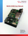
1
ARMFSC2 ARM CORTEX A8 CPU BOARD w/Freescale i.MX53x USER’S MANUAL REV 2.0 © CJB ~ 2014 ARMFSC2_ARM CPUBOARD MANUAL 2.0 page 1 INDEX 1 LIST OF FIGURES ................................................................................................................................................. 4 2 THE C2 CPU BOARD ............................................................................................................................................ 7 2.1 INTRODUCTION ............................................................................................................................................... 7 2.2 FEATURES...................................................................................................................................................... 8 2.3 BLOCK SCHEMATIC ..................................................................................................................................... 9 2.4 TOP SIDE VIEW...........................................................................................................................................10 2.5 BOTTOM SIDE VIEW ...................................................................................................................................11 2.6 OVERVIEW OF ONBOARD FEATURES ..........................................................................................................12 2.6.1 RS-485~422 ISOLATED COM1 PORT .......................................................................................................12 2.6.2 RS232/422/485 NON ISOLATED COM2 PORT..........................................................................................12 2.6.3 CANBUS INTERFACE ...............................................................................................................................12 2.6.4 GPIOs ....................................................................................................................................................12 2.6.5 LVDS General Purpose Port ....................................................................................................................12 2.6.6 TTL LCD Port ..........................................................................................................................................12 2.6.7 1-Wire INTERFACE (OPTIONAL) ..............................................................................................................12 2.6.8 Ethernet Ports .......................................................................................................................................12 2.6.9 Extensive Feature Selectable by Pin-Headers ..........................................................................................12 2.6.10 Wide Range Power Supply .................................................................................................................12 3 JUMPER SETTINGS OF THE C2 ............................................................................................................................13 3.1 JUMPER TOPOLOGY OF THE C2 CPU BOARD (TOP) ..........................................................................................13 3.2 JUMPER TOPOLOGY OF THE C2 CPU BOARD (BOTTOM)...................................................................................14 3.2.1 HOW TO RECOGNIZE PIN 1 (JUMPERS & CONNECTORS) .........................................................................14 3.3 POWER SELECTION JUMPERS .....................................................................................................................15 3.3.1 OVERVIEW OF POWER ROUTING JUMPERS ............................................................................................15 3.3.2 POWER SUPPLY ROUTING FOR THE FULL-FEATURED C2 .........................................................................16 3.3.2.1 3.3.2.2 3.3.2.3 3.3.2.4 3.3.2.5 3.3.2.6 3.3.2.7 JVLCD_5/3 (C2 Full only) ............................................................................................................................... 16 J12V1 and J12V2 (C2 Full only) ...................................................................................................................... 17 JLVDS_PWR (C2 Full only) ............................................................................................................................. 18 BACKLIGHT SELECTION (C2 Full only)............................................................................................................. 19 JINV (C2 Full only)......................................................................................................................................... 19 JLCD7_P3 (C2 Full only)................................................................................................................................. 20 JLCD7_P1 and JLCD7_P2 (C2 Full only) .......................................................................................................... 21 3.3.3.1 3.3.3.2 3.3.3.3 3.3.3.4 3.3.3.5 JLVDS_PWR (DEPOPULATED C2 only) ............................................................................................................ 23 BACKLIGHT SELECTION (DEPOPULATED C2)................................................................................................... 23 JINV ............................................................................................................................................................. 24 JLCD7_P3 ..................................................................................................................................................... 25 JLCD7_P1 and JLCD7_P2 ............................................................................................................................... 26 3.3.3 POWER SUPPLY ROUTING FOR DEPOPULATED C2 ..................................................................................22 3.4 OTHER JUMPERS (FULL & DEPOPULATED C2) ...................................................................................................27 3.4.1 JPWM ...................................................................................................................................................27 3.4.2 JCOM2 ..................................................................................................................................................27 3.4.3 JP_485_REC_EN.....................................................................................................................................28 3.4.4 JP_485_TERMINATION ..........................................................................................................................28 3.4.5 JP_485_RTS_CHOICE .............................................................................................................................28 3.4.6 JCAN_RS ................................................................................................................................................28 3.4.7 J120R_CAN ............................................................................................................................................28 3.4.8 JBAT_EN ................................................................................................................................................29 4 CONNECTORS ....................................................................................................................................................30 4.1 CONNECTOR TOPOLOGY OF THE C2 CPU BOARD (TOP) ...................................................................................30 4.2 TOPOLOGY OF THE C2 CPU BOARD (BOTTOM) ................................................................................................31 4.2.1 HOW TO RECOGNIZE PIN 1 (CONNECTORS & JUMPERS) .........................................................................31 4.3 DC_IN POWER SUPPLY CONNECTOR ..........................................................................................................32 4.4 COM2 DSUB9M SERIAL PORT (RS232/422/485) CONNECTOR .....................................................................33 4.4.1 COM2 JUMPER SETTINGS: the JCOM2 pin header ..................................................................................34 4.4.1.1 4.4.1.2 SETTING JUMPERS TERMINATION & SLEW-RATE: .......................................................................................... 34 SETTING JUMPERS FOR RS232 or RS485 or RS422 COM2 MODE .................................................................... 34 ARMFSC2_ARM CPUBOARD MANUAL 2.0 page 2 4.4.2 Explanation of RS485 Settings................................................................................................................35 4.5 COM1 ISOLATED SERIAL PORT (RS485) CONNECTOR ..................................................................................36 4.5.1 COM1 Pin Assignment ...........................................................................................................................36 4.5.2 COM1 Settings.......................................................................................................................................37 4.5.2.1 Termination Jumper Setting for COM1.......................................................................................................... 37 4.23.1.1 4.23.1.2 Interface for 7” LCD with onboard LED driver ................................................................................................ 59 Interface for 7” LCD with external LED driver ................................................................................................ 60 4.6 USB_A, USB_B USB TYPE_A HOST CONNECTORS ........................................................................................38 4.7 USB_D, USB_E USB AUX HOST PIN HEADER CONNECTORS ..........................................................................39 4.8 LAN1, LAN2 FAST ETHERNET #1 & #2 CONNECTORS, RJ45 ...........................................................................40 4.9 CAN, CAN-V CANBUS INTERFACE CONNECTORS .............................................................................................41 4.9.1 CANbus Interface Settings......................................................................................................................42 4.10 VGA (VGA PIN HEADER CONNECTOR)...........................................................................................................43 4.11 LVDS CONNECTOR .....................................................................................................................................44 4.12 INV (INVERTER / LED DRIVER POWER CONNECTOR) ....................................................................................45 4.12.1 Analysis of the INV Connector’s signals ..............................................................................................46 4.12.2 Pin Assignment for INV connector......................................................................................................46 4.13 AUDIO CONNECTOR...................................................................................................................................47 4.14 SPI1 CONNECTOR.......................................................................................................................................48 4.15 UART_DEBUG PORT ...................................................................................................................................49 4.16 USB-OTG CLIENT USB DEBUG CONNECTION ...............................................................................................50 4.16.1 OTG CABLE EXAMPLE: .......................................................................................................................50 4.17 1W 1-WIRE PERIPHERAL CONNECTOR (OPTIONAL).....................................................................................51 4.18 RESET EXTERNAL RESET CONNECTOR.........................................................................................................52 4.19 SW3 MANUAL RESET PUSHBUTTON...........................................................................................................52 4.20 SW4 - USER DEFINED INPUT #1 (ONLY FOR C2 DEPOPULATED) ........................................................................53 4.21 GPIO TTL I/O CONNECTOR..........................................................................................................................54 4.21.1 TTL GPIO WIRING ..............................................................................................................................55 4.21.2 GPIO Mapping from iMX53................................................................................................................56 4.22 3G_MALE: PIGGYBACK 3G EXPANSION CONNECTOR (OPTIONAL) ................................................................57 4.23 LCD7 (BOTTOM SIDE) 7” TTL PANEL FLAT CABLE ..........................................................................................58 4.23.1 FLEXIBLE 7” LCD INTERFACE...............................................................................................................59 4.23.2 LED_BL CONNECTOR FOR 7”LCD LED BACKLIGHT.............................................................................61 4.24 TOUCH (BOTTOM) CONNECTORS FOR 4W TOUCH SCRTEEN ........................................................................62 4.24.1 EXTENSION CABLES ...........................................................................................................................63 4.25 SD1 (BOTTOM SIDE) USD MEMORY CARD SOCKET ......................................................................................64 4.26 SD2 (BOTTOM SIDE) SD MEMORY CARD SOCKET ........................................................................................64 5 APPENDIX A: THE DEPOPULATED C2 .................................................................................................................65 5.1 6 FEATURES OF THE DEPOPULATED C2 ..........................................................................................................66 APPENDIX B: QUICK JUMPER SETTING CONFIGURATIONS .................................................................................67 6.1 6.2 6.3 6.4 6.5 6.6 6.7 6.8 C2 DEPOPULATED, +24V DC_IN, 7” TTL LCD (DATA IMAGE) .............................................................................68 C2 DEPOPULATED, +24V DC_IN, 7” TTL LCD (CHI MEI RESISTIVE) .....................................................................69 C2 DEPOPULATED, +24V DC_IN, 7” LVDS LCD (DATA IMAGE) ..........................................................................70 C2 FULL, +24V DC_IN, 7” TTL LCD (DATA IMAGE) ............................................................................................71 C2 FULL, +24V DC_IN, 7” TTL LCD (CHI MEI RESISTIVE)) ....................................................................................72 C2 FULL, +24V DC_IN, 7” LVDS LCD (DATA IMAGE) ..........................................................................................73 C2 FULL, +24V DC_IN, 3.3V LVDS LCD (LCD WITH VCC = 3.3V) .........................................................................74 C2 FULL, +24V DC_IN, 5V LVDS LCD (LCD WITH VCC = 5V) ...............................................................................75 ARMFSC2_ARM CPUBOARD MANUAL 2.0 page 3 1 LIST OF FIGURES Fig. 1 Block Schematic................................................................................................................... 9 Fig. 2 Top Side view: shaded areas show features not stuffed in the depopulated version .......... 10 Fig. 3 Bottom Side view: shaded area shows items not stuffed because optional upon request. .. 11 Fig. 4 Topology of the Board (TOP). Lower Side is the Connector Area....................................... 13 Fig. 5 Examples of Silk-Screen figures to recognize Pin 1 ........................................................... 14 Fig. 6 Power Supply Routing Schematic and default jumper settings (whole board) .................... 15 Fig. 7 Power Supply Routing Schematic of the C2 Full and default jumper settings ..................... 16 Fig. 8 JVLCD_5/3 (C2 Full only)................................................................................................... 16 Fig. 9 J12V1 and J12V2 (C2 Full only) ......................................................................................... 17 Fig. 10 Allowed combinations for J12V1 and J12V2 (C2 Full only) ............................................... 17 Fig. 11 JLVDS_PWR (C2 Full only).............................................................................................. 18 Fig. 12 JLVDS_PWR jumper pin assignment and the 3 possible settings .................................... 18 Fig. 13 Combinations allowed for Jumpers for LCD power (C2 Full only) ..................................... 18 Fig. 14 JINV (C2 Full only) ........................................................................................................... 19 Fig. 15 Combinations allowed for JINV jumper (C2 Full only) ....................................................... 19 Fig. 16 JLCD7_P3 (C2 Full only).................................................................................................. 20 Fig. 17 Onboard LED Driver (for 7” small LCD panels)................................................................. 20 Fig. 18 Possible combinations for JLCD7_P3 jumper (C2 Full only) ............................................. 20 Fig. 19 JLCD7_P1 and JLCD7_P2 (C2 Full only) ......................................................................... 21 Fig. 20 Combinations for JLCD7_P1 and JLCD7_P2 jumpers (C2 Full only)................................ 21 Fig. 21 Power Supply Routing Schematic of the Depopulated C2 ................................................ 22 Fig. 22 JLVDS_PWR (Depopulated C2 only) ............................................................................... 23 Fig. 23 JLVDS_PWR jumper pin assignment and the only setting (C2 Depopulated) ................... 23 Fig. 24 JINV (Depopulated C2) .................................................................................................... 24 Fig. 25 Unique combination allowed for JINV jumper (Depopulated C2) ...................................... 24 Fig. 26 JLCD7_P3 (Depopulated C2) ........................................................................................... 25 Fig. 27 Onboard LED Driver (for 7” small LCD panels)................................................................. 25 Fig. 28 Combinations permitted for JLCD7_P3 jumper (Depopulated C2) .................................... 25 Fig. 29 JLCD7_P1 and JLCD7_P2 (C2 Full) ................................................................................ 26 Fig. 30 Combinations for JLCD7_P1 and JLCD7_P2 jumpers (Depopulated C2) ......................... 26 Fig. 31 Topology of the Board (TOP). Lower Side is the Connector Area. .................................... 30 Fig. 32 Topology of the Board (BOTTOM). Lower Side is the Connector Area. ............................ 31 Fig. 33 Examples of Silk-Screen figures to recognize Pin 1 ......................................................... 31 Fig. 34 Power Supply Connector: DC_IN .................................................................................... 32 Fig. 35 DC_IN Connector: pin assignment ................................................................................... 32 Fig. 36 Schematic of DC_IN circuitry............................................................................................ 32 Fig. 37 The COM2 Connector. Notice the JCOM2 pin-header...................................................... 33 Fig. 38 Signals of the COM2 Connector ....................................................................................... 33 Fig. 39 The “JCOM2” pin-header for COM2 (notice default settings) ............................................ 34 Fig. 40 How to set JCOM2 for different COM2 operation ............................................................. 34 Fig. 41 Typical RS485 Driver/Receiver ........................................................................................ 35 Fig. 42 RS422 modified for RS485 with TX data instant read-back .............................................. 35 Fig. 43 The COM1 Connector (Isolated RS485 Serial Port) ......................................................... 36 Fig. 44 COM1 Connector pin assignment..................................................................................... 36 Fig. 45 Schematic of COM1 interface........................................................................................... 36 Fig. 46 COM1 Jumper Setting. Notice the two jumpers which must never be changed ................ 37 Fig. 47 The USB_A and USB_B Type_A USB ports .................................................................... 38 Fig. 48 Schematic of the Connector used for USB_A and USB_B................................................ 38 Fig. 49 The USB_D and USB_E Pin-headers for onboard additional USB ports .......................... 39 Fig. 50 USB_D and USB_E wiring ............................................................................................... 39 Fig. 51 RJ45 Ethernet Ports ......................................................................................................... 40 Fig. 52 Pin Assignment of ETH0 and ETH1 RJ45 Ethernet ports ................................................. 40 Fig. 53 CANbus twin connectors .................................................................................................. 41 Fig. 54 Pin Assignment of CANbus connector.............................................................................. 41 Fig. 55 CANbus Settings Jumpers ............................................................................................... 42 Fig. 56 Schematic of CANbus interface ........................................................................................ 42 Fig. 57 Jumper Setting for CANbus interface (default setting is displayed)................................... 42 ARMFSC2_ARM CPUBOARD MANUAL 2.0 page 4 Fig. 58 VGA Connector (Pin Header) ........................................................................................... 43 Fig. 59 Signals of the VGA Pin Header ........................................................................................ 43 Fig. 60 VGA DSUB15F seen from rear side (wire solder side) ..................................................... 43 Fig. 61 The wiring of the VGA port ............................................................................................... 43 Fig. 62 The LVDS Connector ....................................................................................................... 44 Fig. 63 Signals of the LVDS Connector ........................................................................................ 44 Fig. 64 The INV Connector (for Inverter/LED-driver Power) ......................................................... 45 Fig. 65 Schematic of the circuit around the INV connector ........................................................... 45 Fig. 66 PWM control by variable duty factor ................................................................................. 46 Fig. 67 The Audio Connector ....................................................................................................... 47 Fig. 68 Pin Assignment of the Audio Connector ........................................................................... 47 Fig. 69 Circuitry of the Audio Connector; note the orientation and pin numbers! .......................... 47 Fig. 70 SPI1 Connector; note the orientation and pin numbers! ................................................... 48 Fig. 71 SPI1 Connector wiring and level translator U35 ............................................................... 48 Fig. 72 The “UART_Debug” Connector ........................................................................................ 49 Fig. 73 Example of USBCOM(TTL1.8V) conversion cable........................................................ 49 Fig. 74 Schematic of the Debug Port Connector .......................................................................... 49 Fig. 75 USB_OTG Connector....................................................................................................... 50 Fig. 76 USB_OTG Cable example ............................................................................................... 50 Fig. 77 Optional 1W Connector .................................................................................................... 51 Fig. 78 Optional 1W Connector .................................................................................................... 51 Fig. 79 RESET Connector and Manual Reset Pushbutton (SW3) ................................................ 52 Fig. 80 Schematic of the RESET Connector and SW3 Pushbutton .............................................. 52 Fig. 81 SW4 Box Header Connector (Depopulated C2 only) ........................................................ 53 Fig. 82 SW4 Box Header Connector (Depopulated C2 only) – See Pin 1..................................... 53 Fig. 83 The GPIO Connector........................................................................................................ 54 Fig. 84 The GPIO Connector: wiring and signals involved............................................................ 55 Fig. 85 The GPIO Connector: mapping of the signals involved .................................................... 56 Fig. 86 Layout of the 3G piggyback board .................................................................................... 57 Fig. 87 Schematic of the 3G piggy board interface connector ...................................................... 57 Fig. 88 The LCD7 Connector: designed for instant connection of a 7” LCD.................................. 58 Fig. 89 The 40pin FPC cable connect the C2 to the TTL 7” LCD.................................................. 58 Fig. 90 Typical 40 pin connector of a 7” LCD with onboard LED driver......................................... 59 Fig. 91 Typical 40 pin connector of a 7” LCD without onboard LED driver.................................... 60 Fig. 92 The LED_BL connector for powering 7” backlight............................................................. 61 Fig. 93 The 7” LCD and the C2 assembled together .................................................................... 61 Fig. 94 The 3 types of 4W touch-screen connectors: 2.54mm header, 1.0mm and 0.5mm FPC .. 62 Fig. 95 The 4W touch-screen connectors for FPC cable: 1.0mm and 0.5mm FPC ....................... 62 Fig. 96 The 4W touch-screen connector for 2.54mm flat cable..................................................... 63 Fig. 97 Extension Cable for LCD Backlight................................................................................... 63 Fig. 98 Extension Cable for 4W touch .......................................................................................... 63 Fig. 99 µSD Flash Card Socket (Bottom Side) ............................................................................. 64 Fig. 100 SD Flash Card Socket (Bottom Side) ............................................................................. 64 Fig. 101 3D view of the Depopulated & Coated C2 ...................................................................... 65 Fig. 102 Coating Protection for Touch (left) and TTL LCD (right) connectors ............................... 65 Fig. 103 Coating Protection for uSD/SD (left) and LVDS LCD (right) connectors ......................... 65 Fig. 104 C2 DEPOPULATED, +24V DC_IN, 7” TTL LCD Data Image ......................................... 68 Fig. 105 C2 DEPOPULATED, +24V DC_IN, 7” TTL LCD Chi Mei (Resistive Touch) ................... 69 Fig. 106 C2 DEPOPULATED, +24V DC_IN, 7” LVDS LCD Data Image....................................... 70 Fig. 107 C2 DEPOPULATED, +24V DC_IN, 7” TTL LCD Data Image ......................................... 71 Fig. 108 C2 DEPOPULATED, +24V DC_IN, 7” TTL LCD Chi Mei Resistive ................................ 72 Fig. 109 C2 FULL, +24V DC_IN, 7” LVDS LCD Data Image ........................................................ 73 Fig. 110 C2 FULL, +24V DC_IN, 7” LVDS LCD (with Vcc = 3.3Vdc) ............................................ 74 Fig. 111 C2 FULL, +24V DC_IN, 7” LVDS LCD (with Vcc = 5Vdc) ............................................... 75 ARMFSC2_ARM CPUBOARD MANUAL 2.0 page 5 ARMFSC2_ARM CPUBOARD MANUAL 2.0 page 6 2 THE C2 CPU BOARD 2.1 Introduction The C2 is a powerful and versatile ARM Freescale iMX536 CPU board. It has been designed and manufactured by CJB to provide a flexible computing core to be used for small to medium controllers. A “Controller” is a system where CJB supplies the C2 together with an HMI unit (LCD + touch) and all the necessary software for the appliance’s process management: http://www.cjb.it/en/products/powerplc/powerplcbridge CJB also provides an extensive support for QT-Library (Embedded Linux) or .NET Compact Framework (CE7). Usually the C2 drives a number of peripherals thanks to its versatile I/O features: Ethernet or serial COM port (RS485) for Modbus, and CAN for CANopen modules. The board has also 25 onboard GPIOs (TTL level) which can be easily conditioned (externally) for local I/O management. The wide power supply range (DC 12~36V [*]) and operating temperature (-20ºC ~ +70ºC) and the capability to drive LCD panels of any size up to Full-HD resolution make the C2 the most reliable and versatile choice for applications like: - Professional food appliances (Ovens, Steam boilers, refrigerators, ice-cream, etc.) Vending machines (especially outdoor) Parking, ticketing machines (especially outdoor) Controllers for building & home automation Small & medium sized controllers [*] some limitation of usage with some LCD panels may occur if the DC_IN is lower than 16Vdc © CJB 2013, 2014 ARMFSC2_ARM CPUBOARD MANUAL 2.0 page 7 2.2 Features The C2 Freescale iMX53 CPU board has these features (evidenced features in Italic style are not stuffed in the depopulated version): • • • • • • • • • • • • • • • • • • • • • • • • Freescale iMX536 (optional: i.MX535) 1GB RAM onboard 128kB SPI-RAM (static) for permanent storage of data with unlimited write cycles, with battery backup (uses the same battery which keeps the Real Time Clock running) UARTS: o 1 x RS485/RS-422 optically insulated o 1 x RS232 general purpose COM port, not insulated, selectable also as RS422/485 2 x USB ports with Type_A dual-stack connector 90º 2 x USB 4-pin headers for auxiliary functions (placed inside the pcba) 1 x USB OTG for debug purposes 2 x Ethernet 10/100 with RJ45 90º connector (1 Ethernet port in the Depopulated version) 1 x Micro-SD socket (µSD) 1 x SD socket 2 x LCD Interfaces: o 1 x TTL to support 40pin FPC connector for standard 7” 800x480 with LED backlight (with bonded touch 4W), for two standard versions of LCD panels o 1 x LVDS 2ch 24bit to support any kind of LCD panel, up to Full-HD 1 x VGA video port 1 x 4W touch interface for the touch screen (resistive, 4W) 1 x optional 5W/8W resistive touch interface 1 x LED Backlight driver for the 7” LCD (which don’t have onboard DCDC), with PWM dimming 1 x expansion connector for 3G module piggy-back micro board: this will support one 3G (4G) Mini-PCIe card socket and its USIM card socket GPIO: 25 x TTL I/O software selectable as Inputs or Outputs 1 x 1-Wire interface (optional, for Dallas-type sensors) 1 x CANbus interface AUDIO interface: o 1 x stereo Line-Out connection o 1 x MIC in o 1 x stereo Line-In Power-Supply: 12~36Vdc wide range power supply with power for 7” LCD panels. The Full-featured board can also provide 3.3Vdc or 5Vdc or 12Vdc for most common LCD panels, and also 5Vdc or 12Vdc for LED driver or CCFL inverter. Dimensions: 170mm x 130mm Operating System: Embedded Linux, Windows CE7.0 Certifications: CE. Verified for FCC-B. The board is available in different versions: ARM-C2-FULL Full-Optional and ARM-C2-DEP depopulated with only one Ethernet port (instead of two) and limited LCD-Power interface onboard. This depopulated version is mainly designed to suit small 7” HMI controllers. Following page shows the block schematic of the CPU board. ARMFSC2_ARM CPUBOARD MANUAL 2.0 page 8 ARMFSC2_ARM CPUBOARD MANUAL 2.0 Fig. 1 Block Schematic page 9 (B) i.MX536 MCIMX536AVV8C DA9053-3JHA1 (i.MX536 Core Voltage = 1.1V, Auto-Boot, DDR3 1.5V, 11x11mm) (A) i.MX535 MCIMX535DVV1C DA9053-3HHA1 (i.MX535 Core Voltage = 1.25V, Auto-Boot, DDR3 1.5V, 11x11mm) Top side height limited: 20 mm RTC Battery (CR2032/CR2477) Non_Isolated RS232/422/485 (COM2) RS485 (COM1) CANBUS Resistive 5W TOUCH Line In, Mic In Line out ITEMS IN RED SQUARES MUST NOT BE STUFFED FOR DEPOPULATED BOARD OWIRE D7 1W (3 Pin) NOT STUFFED AS DEFAULT FOR ALL BOM VERSIONS ECSPI1 SPI (1 Mb) SATA DO NOT STUFF FOR DEPOPULATED GPIO_17 A3 Buzzer (AC) VGA I2C(3) (A6,B6) L5: UART3_TX L2: UART3_RX L4: UART3_RTS L3: UART3_CTS A4: UART2_TX B5: UART2_RX K3: UART2_RTS i.MX536 only D5: CAN1_RX C4: CAN1_TX I2C(2) (F6,D4) I2S(C5,B3,E7,D6) RTC, 24C02 GPIO 1-25 SP339E Non_Isolated ADM3485E Isolated ADM2587E Non_Isolated PCA82C250 AR1021T-I/SS SGTL5000 (32QFN) MCIMX536AVV8C 19mmx19mm, 0.8mm Pitch (TE-BGA) 800MHz Cortex-A8 Freescale_iMX536 CO-LAY DEP.ONLY DO NOT STUFF FOR FULL VERSION HUB 1=>4 SMSC_LAN9514 USB1 A17,B17 FULL VERSION ONLY DO NOT STUFF FOR DEPOPULATED (4 Ports) USB_OTG (Box-header) Peripheral mode SMSC LAN8720A LVDS 24 bit Dual Channel Inverter or DCDC TTL 40 PIN FPC CONN. LED Driver AT1316 Auto-Boot, 11mmx11mm, 0.8mm Pitch DA9053 SD Micro SD 1GB DDR3-800 (256MB x4 chips) USB_OTG B19,A19 FEC LVDS EN,PWM DISP0 GPIO PWM I2C2 SD2 4 bit SD1 4 bit DDR3-800 7" LCD connector type same as Colibri, same as AM board BOTTOM SIDE NOT STUFFED AS DEFAULT FOR ALL BOM VERSIONS connector type same as Colibri, for the 7" panel - BOTTOM SIDE connector type same as Colibri, for the 7" panel - BOTTOM SIDE 4 Wires 5 Wires connector type same as AM board TOP SIDE MINI CARD (3G Module) Pin-header Pin-header USB connector (A-Type stack) LAN2 RJ-45 (10/100 MHz) SIM Card Friday , May 02, 2014 ARMFSC2 Document Number Size C Sheet Block Diagram CJB Date: Title DO NOT STUFF FOR DEPOPULATED Daughter board (67.31 x 47.5 mm) USB4 USB3 USB1,USB 2 DO NOT STUFF FOR DEPOPULATED LAN1 RJ-45 (10/100 MHz) LVDS24 U33, U34: DO NOT STUFF FOR DEP. VERSION LCD7 LED Backlight LED_BL Touch screen AR1021 Touch screen Micron_MT41K128M16JT-125:K (1.35V), (Backward-compatible to 1.5V) MICRON_MT41J128M16HA-15E (EVB)--> EOL 2 of 29 Rev B000 2.3 BLOCK SCHEMATIC 2.4 TOP SIDE VIEW USBD USBE CAN GPIO LAN2 ETH1 LAN1 ETH0 AUDIO USBA/B COM1 COM2 DC_IN Fig. 2 Top Side view: shaded areas show features not stuffed in the depopulated version ARMFSC2_ARM CPUBOARD MANUAL 2.0 page 10 2.5 BOTTOM SIDE VIEW Touch 4W 0.5mm FPC Touch 4W 1mm FPC Touch 4W 2.54mm Touch 5W (optional) TTL LCD 7” FPC cable 7” Backlight drive SD Micro-SD Fig. 3 Bottom Side view: shaded area shows items not stuffed because optional upon request. ARMFSC2_ARM CPUBOARD MANUAL 2.0 page 11 2.6 OVERVIEW OF ONBOARD FEATURES 2.6.1 RS-485~422 ISOLATED COM1 PORT The 1st UART (COM1) is RS485/RS422 selectable, and is the main peripheral interface port which will communicate (e.g.: by Modbus-RTU) with external peripherals. This is optically insulated to avoid communication troubles. 2.6.2 RS232/422/485 NON ISOLATED COM2 PORT The 2nd UART (COM2) is RS232/485/RS422 selectable, and is the general purpose COM port interface. The choice (232/422/485) is made by simple jumper setting (JCOM2 pin header). 2.6.3 CANBUS INTERFACE The board has a CANbus port, made from the native CANbus interface of the iMX536. 2.6.4 GPIOs 25 TTL (3.3V) GPIOs are wired to a 44-pin header connector, and can be used for an external I/O conditioning board (user’s designed). All GPIOs come from direct GPIO ports of the iMX53x. Furthermore, another GPIO is used for Backlight control, and another one is used for the Buzzer. 2.6.5 LVDS General Purpose Port The 24Bit 2-Chan LVDS port is provided to interface almost all kinds of commonly available LVDS panels. It can handle up to 2-Channel 24Bits Full-HD. 2.6.6 TTL LCD Port This 18Bit TTL LCD port is designed to make a snap connection through a 40pin FPC cable for standard 7” 800x480 LCD panels with LED backlight. A suitable LED driver for such panels is provided onboard or can be powered by 5Vdc (most new panels have embedded LED driver). 2.6.7 1-Wire INTERFACE (OPTIONAL) This is a native interface of the iMX535, available to connect sensors like Dallas or like devices. 2.6.8 Ethernet Ports There are two 10/100Mb Ethernet Ports (1 only for the depopulated version) available from RJ45 connectors. 2.6.9 Extensive Feature Selectable by Pin-Headers A number of pin-headers allow easy selection of onboard features, to fit the needs of each application (panel power selection, backlight selection, COM port settings and so on). 2.6.10 Wide Range Power Supply The board can be powered by 12~36Vdc wide range power supply. ARMFSC2_ARM CPUBOARD MANUAL 2.0 page 12 3 JUMPER SETTINGS of the C2 This Chapter details all the onboard Jumpers of the C2 and their settings. 3.1 JUMPER TOPOLOGY of the C2 CPU Board (TOP) Please always refer to the board TOP topology as from below drawing. UPPER SIDE LEFT SIDE RIGHT SIDE LOWER SIDE Fig. 4 Topology of the Board (TOP). Lower Side is the Connector Area. ARMFSC2_ARM CPUBOARD MANUAL 2.0 page 13 3.2 JUMPER TOPOLOGY of the C2 CPU Board (BOTTOM) There are no Jumpers on bottom side. 3.2.1 HOW TO RECOGNIZE PIN 1 (JUMPERS & CONNECTORS) To recognize Pin 1 of Connectors & Jumpers, the rules are the following: 1) 2) 3) 4) Pin 1 of Jumpers is evidenced by a bold square around Pin 1 of Connectors is evidenced by a bold marking at side of Pin 1 Underneath (BOTTOM Side) Pin 1 has always a square pad (others have round pads) In most cases, where there is room, pins are numbered. Fig. 5 Examples of Silk-Screen figures to recognize Pin 1 ARMFSC2_ARM CPUBOARD MANUAL 2.0 page 14 3.3 POWER SELECTION JUMPERS Before going to describe the jumper settings, it’s very important to understand the POWER SCHEME of the C2, since there are many jumpers which can affect the behavior of the board, and their settings must be correct, otherwise the board can be damaged. 3.3.1 OVERVIEW OF POWER ROUTING JUMPERS The image below shows the whole power distribution scheme for the C2 FULL version. Main DC power input is from DC_IN connector, which is protected by fuse and by a Varistor. The board is NOT protected against polarity inversion. +5V VDC 1 1 2 3 JLCD7_P1 1 2 3 JLCD7_P2 +5V FUSE1 FUSE 12A/65V U31 DC_IN_POWER 2 +3.3V 3 DC_IN JP (2-4) : +5V or +3.3V JP (3-4) : +3.3V <==== Default JP (4-6) : +12V or +5V TZ1 P6SMB39CAT3 +3.3V JLVDS_PWR 1 3 5 U32 Case GND 1 2 3 4 5 6 Power for LCD logic FUSE2 FUSE 3A/125V 2 4 6 +VLVDS JLCD7_P2 1 2 3 1 2 3 JLCD7_P1 SETTING FOR DATA IMAGE 7" LCD SELECTABLE VLCD POWER: +5V OR +3.3V OR +12V (2nd STAGE) JLCD7_P2 1 2 3 1 2 3 JLCD7_P1 VLCD_+5V or +3.3V SELECTABLE VLCD POWER: 5V OR 3.3V (1st STAGE) SETTING FOR CHIMEI 7" LCD WITH RESISTIVE TOUCH U33 3 1 Select +5V (1-2) Select +3.3V (2-3) <== Default (DEFAULT) JVLCD_5/3 2 2 3 SELECTABLE DISPLAY BACKLIGHT POWER: 5V OR 12V +5V 1-2: DC_IN = 19V~30V <== Default 2-3: DC_IN = 12V J12V1 Power for Backlight of LCD (Inverter or LED_Driver) 1 1-2: DC_IN = 19V~30V <== Default 2-3: DC_IN = 12V VBACKLIGHT_+12V or +5V 1 U34 2 3 3 1 Select +5V (1-2) <== Default Select +12V (2-3) 3 1 Select +5V (1-2) <============== Default Select +12V (or +5V) from U34 (2-3) JINV J12V2 2 JVLCD_12/5 2 FUSE4 FUSE 4A/125V INV_PWR JLCD7_P3 1 2 3 +5V Select +5V or +12V (from U34) (1-2) Select +5V (2-3) <== Default U50 LED DRIVER FOR 7" LCD 7" LED BACKLIGHT 1 2 3 4 5 6 1 2 INV 3 4 LED_BL Fig. 6 Power Supply Routing Schematic and default jumper settings (whole board) The DC_IN supply must be within 12 ~ 36Vdc range. The first important fact is to know if the board is powered by 12Vdc or by a higher voltage: - If DC_IN is 12Vdc (or anyway under 16Vdc), then it is not possible to use U34 unless it’s set to produce 5Vdc by JLVCD_12/5 (1-2) If DC_IN is over 16Vdc then it’s possible to use U34 for any setting of JVLCD_12/5. U34 is the onboard DCDC to be used for the LCD backlight power of big panels (usually 8.4” and larger), which is typically 12Vdc. So you have also to know which LCD panel you are going to use. Every LCD panel usually needs two voltages: 1. The voltage for its electronics, which is typically 3.3Vdc (up to 15” panels), or 5Vdc (17” to 21”), and even 12Vdc (32”and over) 2. The voltage for the backlight: 5V typically for small panels, 12Vdc for all other panels up to 21”, and 24Vdc for big panels (but in this case you will provide the backlight power directly, not through the C2 circuits, since the currents involved will be too high for the C2). You will use the C2 FULL version for driving small and big panels, while the C2 Depopulated can be used only for small panels (typically: 7”). ARMFSC2_ARM CPUBOARD MANUAL 2.0 page 15 3.3.2 POWER SUPPLY ROUTING FOR THE FULL-FEATURED C2 The FULL version of the C2 CPU board has all the 4 onboard DCDC subsystems (U31, U32, U33 and U34). This version of the C2 has been designed to support small and big LCD panels, since U33 and U34 can supply the necessary power for both panel’s electronics and panel’s backlight. +5V FUSE1 FUSE 12A/65V VDC 1 1 2 3 JLCD7_P1 1 2 3 JLCD7_P2 +5V U31 DC_IN_POWER 2 +3.3V 3 DC_IN JP (2-4) : +5V or +3.3V JP (3-4) : +3.3V <==== Default JP (4-6) : +12V or +5V TZ1 P6SMB39CAT3 +3.3V JLVDS_PWR 1 3 5 U32 Case GND 1 2 3 4 5 6 Power for LCD logic FUSE2 FUSE 3A/125V 2 4 6 +VLVDS JLCD7_P2 1 2 3 1 2 3 JLCD7_P1 SETTING FOR DATA IMAGE 7" LCD SELECTABLE VLCD POWER: +5V OR +3.3V OR +12V (2nd STAGE) JLCD7_P2 1 2 3 1 2 3 JLCD7_P1 VLCD_+5V or +3.3V SELECTABLE VLCD POWER: 5V OR 3.3V (1st STAGE) SETTING FOR CHIMEI 7" LCD WITH RESISTIVE TOUCH U33 1 3 Select +5V (1-2) Select +3.3V (2-3) <== Default (DEFAULT) JVLCD_5/3 2 +5V 2 1-2: DC_IN = 19V~30V <== Default 2-3: DC_IN = 12V J12V1 3 SELECTABLE DISPLAY BACKLIGHT POWER: 5V OR 12V Power for Backlight of LCD (Inverter or LED_Driver) 1 1-2: DC_IN = 19V~30V <== Default 2-3: DC_IN = 12V VBACKLIGHT_+12V or +5V 1 U34 2 3 1 3 Select +5V (1-2) <== Default Select +12V (2-3) 1 3 Select +5V (1-2) <============== Default Select +12V (or +5V) from U34 (2-3) JINV J12V2 2 JVLCD_12/5 2 FUSE4 FUSE 4A/125V INV_PWR JLCD7_P3 1 2 3 +5V Select +5V or +12V (from U34) (1-2) Select +5V (2-3) <== Default U50 LED DRIVER FOR 7" LCD 7" LED BACKLIGHT 1 2 3 4 5 6 1 2 INV 3 4 LED_BL Fig. 7 Power Supply Routing Schematic of the C2 Full and default jumper settings 3.3.2.1 JVLCD_5/3 (C2 Full only) Jumper JVLCD_5/3 allows choosing the voltage for pin 2 of the 6-pin header called JLVDS_PWR where you can select the supply voltage for the LVDS LCD connected to the C2. - Set JVLCD_5/3 for 2-3 (default) if the LCD needs +3.3Vdc (e.g.: 8.4” or 10.4” or 12” or 15”) Set JVLCD_5/3 for 1-2 only if the LCD needs +5Vdc (e.g.: 17” or 19” or 21.5”) Fig. 8 JVLCD_5/3 (C2 Full only) ARMFSC2_ARM CPUBOARD MANUAL 2.0 page 16 3.3.2.2 J12V1 and J12V2 (C2 Full only) Jumpers J12V1 and J12V2 are used to bypass U34 when the C2 is powered by 12Vdc and the voltage for the LCD backlight needs 12Vdc. If the LCD backlight needs 5Vdc then you can use U34, provided the JVLCD_12/5 jumper is correctly set 1-2 (default). Fig. 9 J12V1 and J12V2 (C2 Full only) - Set J12V1 and J12V2 both 2-3 if the C2 Full DC_IN is 12Vdc and backlight needs 12Vdc Set J12V1 and J12V2 both 1-2 if the C2 Full DC_IN is 12Vdc and the backlight needs 5Vdc then set JVLCD_12/5 to 1-2 Set J12V1 and J12V2 both 1-2 if the C2 Full is powered by 16Vdc or more, and the backlight needs 12Vdc then set JVLCD_12/5 to 2-3 Set J12V1 and J12V2 both 1-2 if the C2 Full is powered by 16Vdc or more, and the backlight needs 5Vdc then set JVLCD_12/5 to 1-2 The table here below shows the possible combinations. J12V1 2-3 J12V2 2-3 1-2 1-2 1-2 1-2 1-2 1-2 JVLCD_12/5 Does not care, U34 bypassed 1-2 1-2 2-3 DC_IN Power Supply +12Vdc Effect V-Backlight 12Vdc +12Vdc > 16Vdc > 16Vdc V-Backlight 5Vdc V-Backlight 5Vdc V-Backlight 12Vdc Fig. 10 Allowed combinations for J12V1 and J12V2 (C2 Full only) ARMFSC2_ARM CPUBOARD MANUAL 2.0 page 17 3.3.2.3 JLVDS_PWR (C2 Full only) This is a 6-pin header which allows selecting the correct voltage for the LVDS LCD electronic. You can select the voltage to be +3.3Vdc, +5Vdc and +12Vdc. Refer to the LCD’s datasheet. Fig. 11 JLVDS_PWR (C2 Full only) 1 2 3 4 5 6 default 1 2 1 2 3 4 3 4 5 6 5 6 Fig. 12 JLVDS_PWR jumper pin assignment and the 3 possible settings The connection of JLVDS_PWR for the C2 Full version is sensitive to the settings of jumpers JVLCD_5/3, J12V1, J12V2 and JVLCD_12/5. The table here below shows the possible settings. DC_IN Power Supply +12Vdc or higher +12Vdc or higher +12Vdc or higher J12V1 J12V2 JVLCD_12/5 JVLCD_5/3 Does not care Does not care Does not care Does not care Does not care Does not care Does not care 2-3 (default) 4-6 +12Vdc 2-3 2-3 4-6 +12Vdc 1-2 1-2 4-6 > 16Vdc 1-2 1-2 Does not care Does not care Does not care Does not care since U34 is bypassed 1-2 (default) 1-2 (default) 4-6 > 16Vdc 1-2 1-2 JLVDS_PWR 3-4 (default) 2-4 2-4 2-3 1-2 Does not care Does not care Does not care Does not care Resulting LVDS LCD Power available from LVDS24 conn. 3.3Vdc from U32 (use with small 3.3V LCD only) 3.3Vdc from U33 (use with bigger 3.3V LCD) 5Vdc from U33 (use with bigger 5V LCD) 12Vdc same as DC_IN (use with big LCD like 32”) Make Sure 12Vdc DC_IN has enough current available 5Vdc from U34 (use with bigger 5V LCD) 5Vdc from U34 (use with bigger 5V LCD) 12Vdc from U34 (use with big LCD like 32”) Make Sure DC_IN has enough current Fig. 13 Combinations allowed for Jumpers for LCD power (C2 Full only) ARMFSC2_ARM CPUBOARD MANUAL 2.0 page 18 3.3.2.4 BACKLIGHT SELECTION (C2 Full only) The last step is the choice of the supply for the LCD’s backlight. The involved jumpers are JINV and JLCD7_P3. The first simply selects between +5Vdc and the voltage which exits from J12V2: this voltage is then forwarded to the INV connector, where you will connect the LED driver or the CCFL inverter. The second jumper does the same selection for the onboard LED driver which can be used for the LED backlight of small panels (like 7”). Wrong setting of this jumper can create board’s damage since its setting strictly depends on the setting of J12V1, J12V2 and JVLCD_12/5. 3.3.2.5 JINV (C2 Full only) This jumper will bring the backlight power to pins 1 and 2 of the INV connector. The LCD’s LED Driver or CCFL Inverter will be connected to this INV connector. Table here below shows the allowed settings, since JINV strictly depends on the settings of J12V1, J12V2 and JVLCD_12/5. Fig. 14 JINV (C2 Full only) JINV DC_IN Power Supply J12V1 J12V2 JVLCD_12/5 Available Backlight Power 1-2 (default) Does not care Does not care Does not care Does not care 5Vdc from U31 (use with small LCD choice #1) Does not care since U34 is bypassed 1-2 (default) 1-2 (default) 12Vdc from DC_IN (use with bigger LCD) Make Sure 12Vdc DC_IN has enough current 5Vdc from U34 (use with small LCD choice #2) 5Vdc from U34 (use with small LCD choice #2) 12Vdc from U34 (use with bigger LCD) Make Sure DC_IN has enough current 2-3 +12Vdc 2-3 2-3 2-3 +12Vdc 1-2 1-2 2-3 > 16Vdc 1-2 1-2 2-3 > 16Vdc 1-2 1-2 2-3 Fig. 15 Combinations allowed for JINV jumper (C2 Full only) ARMFSC2_ARM CPUBOARD MANUAL 2.0 page 19 3.3.2.6 JLCD7_P3 (C2 Full only) This jumper’s name reminds its usage is for 7” LCD panels only. Its setting selects the voltage for the onboard LED driver (U50) which is used to power the LED backlight of the 7” panels which don’t have onboard LED driver. The onboard LED driver of the C2 can only run from +5Vdc, otherwise U50 will burn. So it’s mandatory that the JLCD7_P3 setting never feeds 12Vdc (or higher voltage) to U50. Fig. 16 JLCD7_P3 (C2 Full only) VLCD_12/5 LED BACKLIGHT JLCD7_P3 1 2 3 L20 FB180/0603/1500mA 1UH/7A D9 VLED+ B130LAW C281 5V_MAIN C280 10U/8/10V DCDC_3V2 6 4 2 JLCD7_P3(2-3) VIN EN GND LX OVP FB 1 5 3 R299 Ra 1.13/12 Rb 3 4 C282 LED_BL C279 R297 0/12 WW12XR500FTL AT1316 R298 100K/6 U50 R544 X/12/X JPWM 1 (6) DISP0_CONTRAST 1 2 L21 PWM-D2_DIM-CTRL VLED- 2 3 LVDS24_PWM (11) H1X3/2.0mm JPWM(2-3) DIM-CTRL = LOW => LAMP OFF DIM-CTRL = HIGH => LAMP ON DIM-CTRL = 100Hz ~ 1kHz => DIMMING Fig. 17 Onboard LED Driver (for 7” small LCD panels) JLCD7_P3 DC_IN Power Supply J12V1 J12V2 JVLCD_12/5 Available Backlight Power 2-3 (default) Does not care Does not care Does not care Does not care 5Vdc from U31 (use with small LCD choice #1) 1-2 +12Vdc 2-3 2-3 1-2 +12Vdc 1-2 1-2 1-2 > 16Vdc 1-2 1-2 1-2 > 16Vdc 1-2 1-2 Does not care 1-2 (default) 1-2 (default) 2-3 NOT ALLOWED 5Vdc from U34 (use with small LCD choice #2) 5Vdc from U34 (use with small LCD choice #2) NOT ALLOWED Fig. 18 Possible combinations for JLCD7_P3 jumper (C2 Full only) ARMFSC2_ARM CPUBOARD MANUAL 2.0 page 20 3.3.2.7 JLCD7_P1 and JLCD7_P2 (C2 Full only) These jumpers simply choose which TTL 7” LCD panel can be connected to the C2 (Full). Fig. 19 JLCD7_P1 and JLCD7_P2 (C2 Full only) The setting of these jumpers is not affected by the setting of any other jumpers described before. There are only two allowed settings: JLCD7_P1 and JLCD7_P2 1-2 Both (default) 2-3 Both Selected TTL 7” LCD Panel LCD with onboard LED driver which needs 5Vdc (like Data Image TTL 7” LCD) LCD without onboard LED driver (like Chimei TTL 7” LCD) Fig. 20 Combinations for JLCD7_P1 and JLCD7_P2 jumpers (C2 Full only) Usually, 7” TTL LCD panels which don’t have onboard LED driver are the cheapest ones and often they have bonded 4W resistive touch. ARMFSC2_ARM CPUBOARD MANUAL 2.0 page 21 3.3.3 POWER SUPPLY ROUTING FOR DEPOPULATED C2 The DEPOPULATED version of the C2 CPU board has only 2 onboard DCDC subsystems (U31 and U32). This version of the C2 has been designed to support small LCD panels, typically just only 7” TTL panels (or also 7” LVDS), which power can be supplied by U31 and U32 with no problem of overload. U33 and U34, and also J12V1, J12V2, JVLCD_12/5, JVLCD_5/3 are not stuffed. +5V 1 VDC 1 2 3 JLCD7_P1 1 2 3 JLCD7_P2 +5V FUSE1 FUSE 12A/65V U31 DC_IN_POWER 2 +3.3V 3 DC_IN JP (2-4) : +5V or +3.3V JP (3-4) : +3.3V <==== Default JP (4-6) : +12V or +5V TZ1 P6SMB39CAT3 +3.3V Power for LCD logic JLVDS_PWR 1 3 5 U32 Case GND FUSE2 FUSE 3A/125V 2 4 6 1 2 3 4 5 6 +VLVDS SELECTABLE VLCD POWER: +5V OR +3.3V OR +12V (2nd STAGE) JLCD7_P2 1 2 3 1 2 3 JLCD7_P1 SETTING FOR DATA IMAGE 7" LCD JLCD7_P2 1 2 3 1 2 3 JLCD7_P1 SETTING FOR CHIMEI 7" LCD WITH RESISTIVE TOUCH (DEFAULT) +5V 3 1 Select +5V (1-2) <============== Default Select +12V (or +5V) from U34 (2-3) JINV 2 FUSE4 FUSE 4A/125V INV_PWR JLCD7_P3 1 2 3 +5V Select +5V or +12V (from U34) (1-2) Select +5V (2-3) <== Default U50 LED DRIVER FOR 7" LCD 7" LED BACKLIGHT 1 2 3 4 5 6 1 2 INV 3 4 LED_BL Fig. 21 Power Supply Routing Schematic of the Depopulated C2 Notice that JLCD7_P3 is 2-3 by default, but if removed or set 1-2 then U50 will not be driven. This can save onboard power and minimize emissions if you don’t use the LED_BL connector. JINV must be 1-2 and the only backlight power available from INV connector is +5Vdc. Basically, the Depopulated C2 has been manufactured for small systems with 7” panels only. ARMFSC2_ARM CPUBOARD MANUAL 2.0 page 22 3.3.3.1 JLVDS_PWR (DEPOPULATED C2 only) This is a 6-pin header which allows selecting the correct voltage for the LVDS LCD electronic. You can only select +3.3Vdc. The default 2-3 setting is already what you need. It’s only valid for small LVDS panels. The TTL interface is not affected by this jumper setting. Fig. 22 JLVDS_PWR (Depopulated C2 only) 1 2 3 4 5 6 default Fig. 23 JLVDS_PWR jumper pin assignment and the only setting (C2 Depopulated) 3.3.3.2 BACKLIGHT SELECTION (DEPOPULATED C2) The choice of the supply for the LCD’s backlight still involves jumpers JINV and JLCD7_P3. The first simply selects the +5Vdc and forwards to the INV connector, where you will connect the LED driver or the CCFL inverter of the 7” panel. The second jumper does the same selection for the onboard LED driver U50 which can be used for the LED backlight of 7” panels which don’t have any LED driver onboard. The unique allowed setting is 1-2 (default), unless you don’t want to power up U50. Next chapters will detail the settings. ARMFSC2_ARM CPUBOARD MANUAL 2.0 page 23 3.3.3.3 JINV This jumper will bring the backlight power to pins 1 and 2 of the INV connector. The LCD’s LED Driver or CCFL Inverter will be connected to this INV connector. For 7” LCD panels, the INV connector is used mainly to supply the +5Vdc for LVDS version of the 7” LCD panels. In fact, many 7” LCD panels which have onboard LED driver are TTL, and the onboard driver gets the +5V from the same 40 pin cable of the TTL signals. If the 7” LCD is LVDS, the main cable from the LVDS connector of the C2 cannot give both voltages (3.3Vdc and 5Vdc) so you have to get the backlight voltage from the INV connector. And here pins 1 and 2 get the +5Vdc selected by JINV (set for 1-2). Fig. 24 JINV (Depopulated C2) JINV DC_IN Power Supply 1-2 (default) Does not care OPEN Does not care J12V1 J12V2 Does not care Does not care Does not care Does not care JVLCD_12/5 Available Backlight Power to INV connector Does not care 5Vdc from U31 (use with small LCD) Does not care No power to INV connector Fig. 25 Unique combination allowed for JINV jumper (Depopulated C2) ARMFSC2_ARM CPUBOARD MANUAL 2.0 page 24 3.3.3.4 JLCD7_P3 This jumper’s name reminds its usage is for 7” LCD panels only. Its setting selects the voltage for the onboard LED driver (U50) which is used to power the LED backlight of the 7” LCD panels which don’t have onboard LED driver. Fig. 26 JLCD7_P3 (Depopulated C2) The onboard LED driver of the C2 can only run from +5Vdc. The JLCD7_P3 setting can be only 2-3. If JLCD7_P3 is set 1-2 in the Depopulated C2, the onboard LED driver U50 will not be active. VLCD_12/5 LED BACKLIGHT JLCD7_P3 1 2 3 L20 FB180/0603/1500mA 1UH/7A D9 VLED+ B130LAW L21 C281 5V_MAIN C280 10U/8/10V DCDC_3V2 6 4 2 JLCD7_P3(2-3) VIN EN GND LX OVP FB 1 5 3 Ra 1.13/12 Rb 3 4 LED_BL C279 R297 0/12 WW12XR500FTL AT1316 R298 100K/6 U50 R544 X/12/X JPWM PWM-D2_DIM-CTRL 1 (6) DISP0_CONTRAST R299 1 2 C282 VLED- 2 3 LVDS24_PWM (11) H1X3/2.0mm JPWM(2-3) DIM-CTRL = LOW => LAMP OFF DIM-CTRL = HIGH => LAMP ON DIM-CTRL = 100Hz ~ 1kHz => DIMMING Fig. 27 Onboard LED Driver (for 7” small LCD panels) JLCD7_P3 2-3 OPEN Available Backlight Power 5Vdc from U31 (use with small LCD choice #1) Onboard LED Driver (U50) is disabled (remove cap from Jumper JLCD7_P3 if using LVDS 7” LCD panel) Fig. 28 Combinations permitted for JLCD7_P3 jumper (Depopulated C2) ARMFSC2_ARM CPUBOARD MANUAL 2.0 page 25 3.3.3.5 JLCD7_P1 and JLCD7_P2 These jumpers simply choose which TTL 7” LCD panel can be connected to the C2 (Depopulated). Fig. 29 JLCD7_P1 and JLCD7_P2 (C2 Full) The setting of these jumpers is not affected by the setting of any other jumpers described before. There are only two allowed settings: JLCD7_P1 and JLCD7_P2 1-2 Both (default) 2-3 Both Selected TTL 7” LCD Panel LCD with onboard LED driver which needs 5Vdc (like Data Image TTL 7” LCD) LCD without onboard LED driver (like ChiMei TTL 7” LCD) Fig. 30 Combinations for JLCD7_P1 and JLCD7_P2 jumpers (Depopulated C2) Usually, 7” TTL LCD panels which don’t have onboard LED driver are the cheapest ones and often they have bonded 4W resistive touch. ARMFSC2_ARM CPUBOARD MANUAL 2.0 page 26 3.4 OTHER JUMPERS (Full & Depopulated C2) There are other jumpers on the C2, which will be described here below. The jumper setting is valid for both the FULL version and the DEPOPULATED version. The images here below show the Default Setting of each Jumper. 3.4.1 JPWM Default 1-2 GPIO_1 (PIN B7 uP) controls the Backlight of TTL LCD If JPWM is set 1-2 then GPIO_1 (pin B7 of iMX53) can control the brightness of the TTL 7” panel (both LCD models: with onboard and without onboard LED driver). If JPWM is set 2-3 then GPIO_1 (pin B7 of iMX53) will be connected to the INV connector (pin 4). If JPWM is OPEN, brightness control will be always pulled up to Vcc, hence set to maximum (see also the requirements of the CCFL Inverter or LED-Driver, since some CCFL inverters give max brightness when this signal is close to GND and not to Vcc). 3.4.2 JCOM2 Default 1-2 and 3-4 Set COM2 for RS422 This header allows selecting the behavior of the COM2 serial port. See the relevant chapter. ARMFSC2_ARM CPUBOARD MANUAL 2.0 page 27 3.4.3 JP_485_REC_EN Default 2-3 (RECEIVER ALWAYS ENABLED) 3.4.4 JP_485_TERMINATION Default 1-2 (RS485 LINE TERMINATED) 3.4.5 JP_485_RTS_CHOICE Default 1-2 (INVERTED RTS TO CHIP) These three jumpers set the behavior of the COM1 serial port interface. See the relevant chapter. 3.4.6 JCAN_RS Default 1-2 CAN Slew Rate limited to 500kb/s 3.4.7 J120R_CAN Default 1-2 CAN Line Termination Enabled These two jumpers set the behavior of the CANbus interface. See the relevant chapter. ARMFSC2_ARM CPUBOARD MANUAL 2.0 page 28 3.4.8 JBAT_EN Default 2-3 (battery off) This jumper connects/disconnects the onboard 3V coin battery. Image shows the in-usage position. Restore to parking position (2-3) if the board is in the shelf or not used for a long period. ARMFSC2_ARM CPUBOARD MANUAL 2.0 page 29 4 CONNECTORS 4.1 CONNECTOR TOPOLOGY of the C2 CPU Board (TOP) Please always refer to the board TOP topology as from below drawing. UPPER SIDE POWER RAM ARM iMX536 PMIC LEFT SIDE RIGHT SIDE LOWER SIDE Fig. 31 Topology of the Board (TOP). Lower Side is the Connector Area. ARMFSC2_ARM CPUBOARD MANUAL 2.0 page 30 4.2 TOPOLOGY of the C2 CPU Board (BOTTOM) Please always refer to the board BOTTOM topology as from below drawing. Since we’re looking at the board from bottom side, LEFT and RIGHT sides are reversed. UPPER SIDE RAM RIGHT SIDE LEFT SIDE LOWER SIDE Fig. 32 Topology of the Board (BOTTOM). Lower Side is the Connector Area. 4.2.1 HOW TO RECOGNIZE PIN 1 (CONNECTORS & JUMPERS) To recognize Pin 1 of Connectors & Jumpers, the rules are the following: 5) 6) 7) 8) Pin 1 of Jumpers is evidenced by a bold square around Pin 1 of Connectors is evidenced by a bold marking at side of Pin 1 Underneath (BOTTOM Side) Pin 1 has always a square pad (others have round pads) In most cases, where there is room, pins are numbered. Fig. 33 Examples of Silk-Screen figures to recognize Pin 1 ARMFSC2_ARM CPUBOARD MANUAL 2.0 page 31 4.3 DC_IN POWER SUPPLY CONNECTOR The DC_IN connector is placed near the Lower Left corner. Fig. 34 Power Supply Connector: DC_IN Pin assignment is from right to left (looking from front): 1 = +12Vdc~36Vdc 2 = GND 3 = Frame Ground 3 2 1 Fig. 35 DC_IN Connector: pin assignment This is the schematic portion. Notice the soldered fuse (Fuse 1) near the connector. DCIN: 12Vdc or 19V~30V (Typical 24V) PHOENIX COMBICON 1731688 MC 1,5/ 3-G-3,5-RN or equivalent DC_IN 1 FUSE1 FUSE 12A/65V VDC R75 10K/6 C502 C510 C511 1U/12/50V C501 1U/12/50V OQ0312510300G C198 0.01U/6/50V TZ1 P6SMB39CAT3 0.01U/6/50V Littelfuse_0451012.MRL 3 1000P/6/50V 2 C6 0.1U/6/50V R82 0/8 Case GND Fig. 36 Schematic of DC_IN circuitry Be careful to avoid any DC_IN polarity inversion. R82 normally keeps Case_GND and GND connected together. ARMFSC2_ARM CPUBOARD MANUAL 2.0 page 32 4.4 COM2 DSUB9M SERIAL PORT (RS232/422/485) CONNECTOR This is placed at right of DC_IN connector, lower left edge of the board. Fig. 37 The COM2 Connector. Notice the JCOM2 pin-header Pin assignment is defined here below: CTSB#_232/422TX-/485DRXB_232/422TX+/485D+ RTSB#/422RXTXB_232/422RX+ CTSB#_232/422TX-/485DRTSB#/422RX- 1 6 2 7 3 8 4 9 5 COM2 FB22 A1 B1 FB30/8 DSUB/9P Fig. 38 Signals of the COM2 Connector Pin function depends on jumper setting of the U10 (SP339E) interface chipset. This one gets the rough signals directly from the ARM iMX53x processor (UART3 port). U10 allows choosing between RS232 or RS485 or RS422 according to JCOM2 pin-header. See next page for Jumper settings for: SLEW, TERM, MODE0 and MODE1. ARMFSC2_ARM CPUBOARD MANUAL 2.0 page 33 4.4.1 COM2 JUMPER SETTINGS: the JCOM2 pin header These jumpers are just above the DSUB9M connectors: DCDC_3V2 JCOM2 SP339E_MODE1 SP339E_MODE0 SP339E_SLEW SP339E_TERM 1 3 5 7 2 4 6 8 R362 R363 R361 R290 10K/6 10K/6 10K/6 10K/6 H2X4P/2.0mm/S G11990080050 JCOM2(1-2) JC1X2/2.0mm JCOM2(3-4) Default setiing = RS-422 JC1X2/2.0mm 2013_12_12 Fig. 39 The “JCOM2” pin-header for COM2 (notice default settings) 4.4.1.1 SETTING JUMPERS TERMINATION & SLEW-RATE: • TERM JUMPER (7+8) o CLOSED SETS TERMINATION 120 OHM o OPEN NO TERMINATION • SLEW JUMPER (5+6) o CLOSED ENABLES 250kbps SLEW LIMITING o OPEN disables slew limiting FOR RS485 OR RS422 ONLY 4.4.1.2 SETTING JUMPERS FOR RS232 or RS485 or RS422 COM2 MODE Here is the table for the correct jumper setting of JCOM2 header. The jumpers have 2.0mm pitch. Mode JUMPER MODE-0 Pins 3-4 OPEN SELECTED MODE - JUMPER MODE-1 Pins 1-2 OPEN 1 OPEN CLOSED RS232 2 3a 3b CLOSED CLOSED CLOSED X RS-485 HALF DUPLEX OPEN CLOSED RS-422 FULL DUPLEX DEFAULT CLOSED RS-485 With TX readback DEFAULT RESULTING COM2 FUNCTION ASSIGNMENT NOT ALLOWED 1=DCD, 2=RX, 3=TX, 4=DTR, 5=GND 6=DSR, 7=RTS, 8=CTS, 9=RI 1=DATA2=DATA+ 3=GND 1=TX2=TX+ 3=RX+ 4=RX5=GND 1=TXThis setting is used to have DATA4=RXthe TX’ed data read back at 2=TX+ the same time you transmit. DATA+ 3=RX+ Connect pins 1 + 4 and 2 + 3 5=GND of COM2 DB9 connector. After this, TX-/RX- become DATAand TX+/RX+ become DATA+ Fig. 40 How to set JCOM2 for different COM2 operation Please notice that you can have 4 different settings for COM2. Next chapter will explain in detail. ARMFSC2_ARM CPUBOARD MANUAL 2.0 page 34 4.4.2 Explanation of RS485 Settings Normally the COM2 port settings allow 3 different modes of operation: • RS232 Full duplex, single-ended signals, RX, TX, RTS and CTS for full handshake. Suitable for short range communications since it can pick up a lot of noise. It’s Mode 1 from above table. • RS422 Full-duplex as the RS232, only TX and RX. Signals are differential (TX- and TX+, RX- and RX+) to a very high noise rejection. Allows communication over long distance. It’s Mode 3a from above table. • RS485 allow Half Duplex only. When you transmit you cannot receive. Two wires only: Data+ and Data-. Differential signals to allow a very high noise rejection. Allows communication over long distance. It’s Mode 2 from above table. The major problem of an RS485 communication is that when the transmit driver is on, the receiver is off since they are driven by the same control signal (RTS): direct for TX and inverted for RX. RX DATA- RTS DATA+ TX Fig. 41 Typical RS485 Driver/Receiver This is not so good because you cannot understand when the TX flux has ended and you can exchange the direction of the driver/receiver (changing the level of RTS). When you set the JCOM2 pin header for Mode 2, you get exactly the circuitry shown above. In some cases this is enough, but in many others you need to understand quickly when it’s time to change the direction. Then, you have to use the circuit below: 3 RX 4 DATARTS DATA+ 1 TX 2 Fig. 42 RS422 modified for RS485 with TX data instant read-back This is Mode 3b and the RX receiver is always enabled while you enable the TX driver only when you need to transmit. Since the RX receiver is always enabled, you will read your TX’ed data as soon as it exits from the driver. This mode needs an external wiring (red wires) to the COM2 DB9 connector: connect pins 1+4 and 2+3 and you get the RS485 DATA+ and DATA-. ARMFSC2_ARM CPUBOARD MANUAL 2.0 page 35 4.5 COM1 ISOLATED SERIAL PORT (RS485) CONNECTOR This is placed between the DSUB9M connector and the USB connector, lower left edge of the board. There are 3 jumpers which set some features of the COM port. TERMINATION JUMPER Fig. 43 The COM1 Connector (Isolated RS485 Serial Port) 4.5.1 COM1 Pin Assignment The COM1 pin assignment for RS485 (isolated) is evidenced here below. 5 4 3 2 1 or 3 2 or 4 5 1 Data+ DataIsolated GND Fig. 44 COM1 Connector pin assignment RS485_COM1 422RX+ R366 0/6 422RX- R367 0/6 422TX+/485D+ 422TX-/485D422RX+ 422RX- 1 2 3 4 5 90º 3.5mm 422TX- 1x5,3.5mm/RIGHT 422TX+ GND_485 422TX+/485D+ 422TX-/485D- R368 100/20 1 2 3 JP_485_TERMINATION OQ0512510300G H1X3/2.0mm CON3PA_2MM JP_485_TERMINATION(1-2) JC1X2/2.0mm Fig. 45 Schematic of COM1 interface The COM1 port is an isolated RS485 by default. Eventually it can be also used as RS422 (isolated) but it needs a small h/w modification which can be only made by CJB. Pin-Header JP_485_Termination (circled in RED in upper drawing) allows setting the line termination for the RS485. Setting 1-2 enables the RS-485 termination. Notice: this RS485 interface is already a TX-read-back interface (like mode 3b for COM2). You don’t have to do nothing to set this behaviour which is already by default for COM1. Next paragraph details the Jumper settings for COM1. ARMFSC2_ARM CPUBOARD MANUAL 2.0 page 36 4.5.2 COM1 Settings There are three jumpers to set COM1 functionality: DO NOT CHANGE! TERMINATION JUMPER Fig. 46 COM1 Jumper Setting. Notice the two jumpers which must never be changed The only jumper you are allowed to change is the Termination Jumper. Never change the other two jumpers nearby. 4.5.2.1 Termination Jumper Setting for COM1 The settings are the following: • 1+2 Termination enabled To be set when the C2 is at one end of the daisy-chain of RS485 boards connected each other • 2+3 Termination disabled To be set when the C2 is in a middle position of the daisy-chain of RS485 boards connected each other ARMFSC2_ARM CPUBOARD MANUAL 2.0 page 37 4.6 USB_A, USB_B USB TYPE_A HOST CONNECTORS They are placed between the COM1 and the LAN1 connectors, lower centre edge of the board. Fig. 47 The USB_A and USB_B Type_A USB ports These are common Type_A host connectors. Inside the CPU board circuitry, these are USB Channels 1 and 2. USB-A_USB-B FB18 USBV2 1 USBDN2A_DM 2 USBDN2A_DP 3 FB30/8 USBG2 4 9 11 V0 -D0 +D0 G0 5 6 7 8 G G 1 2 3 4 V1 -D1 +D1 G1 G G 5 6 7 8 USBV3 USBDN3A_DM USBDN3A_DP USBG3 FB19 FB30/8 10 12 DUAL_USB/RIGHT G11990080049 FOXCONN_UB1112C-8FDE-4F FB20 FB30/8 Case GND Fig. 48 Schematic of the Connector used for USB_A and USB_B ARMFSC2_ARM CPUBOARD MANUAL 2.0 page 38 4.7 USB_D, USB_E USB AUX HOST PIN HEADER CONNECTORS They are placed near the lower right corner of the board. Fig. 49 The USB_D and USB_E Pin-headers for onboard additional USB ports These are 4-pin headers wired as below. USBD USBV4 USBDN4A_DM USBDN4A_DP USBG4 FB27 FB30/8 1 2 3 4 JST_ePH, 1x4, 2.0mm B4B-PH-K-S(LF)(SN) USBE USBV5 USBDN5_CONN_DM USBDN5_CONN_DP USBG5 FB38 FB30/8 1 2 3 4 PIN ASSIGNMENT: 1. 2. 3. 4. VCC (red wire) DATA- (white wire) DATA+ (green wire) GND (black wire) JST_ePH, 1x4, 2.0mm B4B-PH-K-S(LF)(SN) Fig. 50 USB_D and USB_E wiring ARMFSC2_ARM CPUBOARD MANUAL 2.0 page 39 4.8 LAN1, LAN2 FAST ETHERNET #1 & #2 CONNECTORS, RJ45 These are two RJ45 connector for onboard Ethernet channel #0 (left) and #1 (right). They are placed in the lower edge of the CPU board, side-to-side each other. Notice: ETH1 (right connector) is stuffed only in the fully populated version of the board. ETH0 ETH1 ETH0 ETH1 Fig. 51 RJ45 Ethernet Ports The signals of each of these ports follow the standard assignment, as you can see here below. TX+ TXRX+ RX- Fig. 52 Pin Assignment of ETH0 and ETH1 RJ45 Ethernet ports The MACaddress for each port has been programmed in factory; the value is the label stuck onto each RJ45 connector block. ARMFSC2_ARM CPUBOARD MANUAL 2.0 page 40 4.9 CAN, CAN-V CANBUS interface CONNECTORS These are placed at right of rightmost Ethernet connector (ETH1), lower right edge of the board. The two connectors have the same pinout, and are in parallel, to allow an easy connection when the C2 is eventually placed in the middle of the daisy-chain of CANbus modules. Fig. 53 CANbus twin connectors The connectors have the following pin assignment: 1. 2. 3. 4. GROUND_CAN (NOT ISOLATED) CAN_H CAN_L n.c. 4 3 2 1 Fig. 54 Pin Assignment of CANbus connector There are two connectors because this makes easy the usage of the board amid a “daisy chain” of CANbus connections. In other words, when the C2 is used not as ending node, but in the mid of the fieldbus, you will have one cable connected from connector CAN (90º connector) to an I/O module and another cable connected from connector CAN-V (vertical) to another module. IMPORTANT NOTICE: if you are using the C2 inside the fieldbus, make sure the termination resistor (J120R_CAN) is not enabled. See following chapter which details the settings of the CANbus interface. ARMFSC2_ARM CPUBOARD MANUAL 2.0 page 41 4.9.1 CANbus Interface Settings There are two jumpers near the 90º CAN connector. They allow for the Line Termination insertion, and for the bus speed limiting. Fig. 55 CANbus Settings Jumpers The schematic here below shows the circuitry of the CANbus interface. The Line Termination resistor must be inserted when the board is at one end of the daisy-chain connection between the CANbus modules. It can be set with Jumper J120R_CAN (the rightmost of the two jumpers): closing 1-2 sets the termination resistor. The JCAN_RS pin header (placed nearby the connector) allows selection of CANbus speed limiting. 2013_06_14 Mount CAN and CAN-V at same time U7 3 CANH RS Vref Vcc CANL 2 C385 0.1U/4 JCAN_RS L32 L33 5 6 R340 121/6/1 CAN0_H CAN0_L Murata_BLM21PG221SN1B 1 2 3 4 1x4,3.5mm/RIGHT D39 OQ0412510300G 1 2 3 G J120R_CAN H1X3/2.0mm 2 27K/6/1 3 SOT23 CAN0_H CAN0_L CON3PA_2MM J120R_CAN(1-2) JC1X2/2.0mm JCAN_RS(1-2) CAN 3 SOIC8A_1-27 1 FB 220/8/2A FB 220/8/2A PESD1CAN PCA82C250 H1X3/2.0mm R6 GND 7 2 5V_CAN TxD RxD 1 Delay setting 8 K2 1 4 K1 CAN_RS CANTX0 CANRX0 1 2 3 4 CAN-V 1x4,3.5mm/Vertical OQ0312500000G JC1X2/2.0mm Fig. 56 Schematic of CANbus interface 1-2 2-3 JCAN_RS J120R_CAN High Speed Low Speed 1-2 2-3 Termination Inserted No Termination Fig. 57 Jumper Setting for CANbus interface (default setting is displayed) ARMFSC2_ARM CPUBOARD MANUAL 2.0 page 42 4.10 VGA (VGA Pin Header CONNECTOR) The VGA interface is made of a 10 (2x5) pin header, 2.0mm pitch, and it’s placed near the mid centre right side of the board. Fig. 58 VGA Connector (Pin Header) VGA IOR IOG IOB VGA_HSY NC VGA_VSY NC 1 3 5 7 9 2 4 6 8 10 VGA_I2C_SDA VGA_I2C_SCL Fig. 59 Signals of the VGA Pin Header You can wire a short cable from this pin-header to a common female DSUB15F, to obtain the common VGA connector like any PC. Connections are the following, seen from the REAR SIDE (solder wire side) of the DSUB15F Female connector: Fig. 60 VGA DSUB15F seen from rear side (wire solder side) SIGNAL NAME RED GREEN BLUE HORIZONTAL VERTICAL GND DATA VGA_I2C_SDA CLOCK VGA_I2C_SCL C2 VGA PIN Header 1 3 5 7 9 6,8,10 2 4 DSUB15F PIN 1 2 3 13 14 5,6,7,8,10 12 15 Fig. 61 The wiring of the VGA port ARMFSC2_ARM CPUBOARD MANUAL 2.0 page 43 4.11 LVDS CONNECTOR This is one 40 pin (2x20) header, and its location is near the left of the VGA connector pin header. The LVDS Port can support 2-Channels, 24-bits LCD panels with resolution up to 1920x1080 (1080p). Fig. 62 The LVDS Connector Since LCD panels may require different power supplies, you have to check the correct jumper settings for LVDS Power before connecting an LCD. The details of the LCD jumper settings are covered in next paragraphs. Ask CJB for pin assignment between the C2 LVDS connector and your panel. Since R213 + R214 are not stuffed and R226 + R227 are, pins 25 and 26 are two ground pins. Fig. 63 Signals of the LVDS Connector The power rail called +VLVDS is the power for the LCD electronics, and the voltage can be selected by the JLVDS_PWR pin header. Default setting is 3.3Vdc (3-4). Figure 1 The Pin Header JLVDS_PWR allows selection of voltage for the LCD Each panel also needs power for the backlight. Details of the relevant connector (INV) are described in next paragraph. ARMFSC2_ARM CPUBOARD MANUAL 2.0 page 44 4.12 INV (INVERTER / LED DRIVER POWER CONNECTOR) This 6 pin 2.5mm pitch male header is the central of the three connectors on upper left edge of the board. Notice that the leftmost connector (“1W”) is optional and it’s never stuffed by factory. The INV connector is used to bring power to LCD’s inverter or LED backlight driver. Usually brings 12Vdc which is the most common voltage for powering Inverters or LED drivers. 1W NOT STUFFED Fig. 64 The INV Connector (for Inverter/LED-driver Power) The schematic here below details how the INV connector has been wired to the typical signals and power rails used for Inverters and for LED drivers. Fig. 65 Schematic of the circuit around the INV connector A detailed discussion of the signals and power rails is in the following paragraph. ARMFSC2_ARM CPUBOARD MANUAL 2.0 page 45 4.12.1 Analysis of the INV Connector’s signals Looking at the schematic of the previous paragraph, you can recognize that: 1. Power Selection: +12/+5 The Inverter/LED-driver power (for pins 1 and 2) can be selected between +5Vdc and +12Vdc by setting the jumper of JINV pin header. 2. Backlight ON/OFF Since usually either an Inverter or a LED-driver need a positive signal for Enable, the INV_EN signal to pin 3 is kept at positive (high) level by default. To shut off the lamps, the GPIO signal “LCD_BLT_EN” must be forced to low level. 3. Dimming for CCFL Inverters Usually CCFL Inverters have limited dimming capabilities: they usually need 0Vdc for max brightness, and 5Vdc (or 3.3Vdc) for min brightness, which usually is only 70% of the max brightness. In this case you can drive the GPIO signal “LVDS24_PWM” either low or high, to have the max or min brightness for the CCFL inverter. Notice that default is min brightness by the pull-up resistor R534. 4. Dimming for LED Drivers LED Drivers often have similar features (behave like the CCFL inverters), but nowadays the most diffused LED Driver models need a Dimming action managed by PWM. That means you will apply a fixed frequency square wave (1 kHz, for example) but with variable duty factor of the square wave: Fig. 66 PWM control by variable duty factor The figure above shows the solid 50% duty-factor square wave which will drive the backlight 50% of the brightness; the red square wave shows an example of ~85%duty factor, where the wave stays at high level for 85% of the cycle. This will drive the brightness to 85%. The green wave shows the opposite, i.e. one 15|% duty factor only, for a 15% of the available brightness. If you drive the PWM input with permanently high signal, you get max brightness, like 100% duty factor; if you drive the PWM input with a permanently low signal, you shut off the backlight (0% brightness). Important: some LED-driver boards do not allow 0% duty factor. They always need a minimal duty factor (like 1% or 2%) otherwise faults can occur. Please get all the needed information for correct drive of your LED-driver board. 4.12.2 Pin Assignment for INV connector This is the pin assignment of the INV connector: 1. 2. 3. 4. +12Vdc (JINV 2-3) or +5Vdc (JINV 1-2) (fused) Default is +5Vdc Same as above pin 1 Enable also called ON/OFF (High = ON) Default is High level PWM (LED) or Brightness (CCFL) Default is High level a. Usually High or 100% PWM sets max brightness to LED Driver boards b. Usually Low or GROUND sets max brightness to CCFL inverter 5. GND 6. GND ARMFSC2_ARM CPUBOARD MANUAL 2.0 page 46 4.13 AUDIO CONNECTOR There is one pin-header, 10 (2x5) pins, 2.0mm pitch, for the Audio interface signals, almost mid centre of the board, just near the innermost mounting hole. Fig. 67 The Audio Connector This connector has all the typical signals of a standard Audio Interface: LINE_OUT LINE_IN MIC_IN 1 = Line_Out_Left 2 = Line_In_Left 10 = MIC_Input 3,5 = GND 4,6 = GND 9 = GND 7 = Line_Out_Right 8 = Line_In_Right Fig. 68 Pin Assignment of the Audio Connector AUDIO Line_IN_L Line_IN_R 2 4 6 8 10 LOUT-L 1 3 5 7 9 MIC_TIP-1 ADO_GND ADO_GND LOUT-R ADO_GND Fig. 69 Circuitry of the Audio Connector; note the orientation and pin numbers! WARNING: Never use the Line_OUT signals to drive a speaker or a headphone. The signals exiting from the C2 are low power and need always to be amplified externally. The MIC_IN should be connected to a common PC electret-condenser mike. ARMFSC2_ARM CPUBOARD MANUAL 2.0 page 47 4.14 SPI1 CONNECTOR The SPI1 connector is one 10-pin header near the USBD header connector, right side of the board. It has the signals which can be used for a high-speed SPI interface, including +3.3V and +5V power supplies (not protected, so be careful when using them to power external devices). Fig. 70 SPI1 Connector; note the orientation and pin numbers! From this header you will have the MOSI (Master Output to Slave Input), the MISO (Master Input from Slave Output), a Serial Clock, and a Chip-Select (ECSPI1_SS1). All signals have a 5V level (since they are translated by U35). Common Ground is available on Pin 7. +3.3V +5V JSPI ECSPI1_SS1_5V ECSPI1_MISO_5V 1 3 5 7 2 4 6 8 ECSPI1_SCLK_5V ECSPI1_MOSI_5V GND Fig. 71 SPI1 Connector wiring and level translator U35 ARMFSC2_ARM CPUBOARD MANUAL 2.0 page 48 4.15 UART_DEBUG PORT To survey the boot up of the board, you must connect the “Debug” port to a PC, where a suitable “Console Simulator” program is running. For example: PUTTY or HyperTerminal or other similar programs. Fig. 72 The “UART_Debug” Connector Since modern PC’s do not have COM ports, it’s suggested to use an USBCOM (TTL1.8V) conversion cable, like the FTDI model TTL-232RG-VREG1V8-WE, which TTL signals commit the 1.8Vdc levels required by the C2 Debug Port. Such cable appears like the photo here below (where we have already wired the small white connector for the Debug Port). Fig. 73 Example of USBCOM(TTL1.8V) conversion cable The schematic of the Debug Port is here below: 1 2 3 4 5 6 Nc Nc GND TX TTL 1.8V GND RX TTL 1.8V Fig. 74 Schematic of the Debug Port Connector When preparing the cable, wire one JST B6B-PH-K 6-pin female so that the TX wire of the conversion cable is connected to pin 6 (RX), the RX wire of the cable is connected to pin 4 (TX), and the Ground wire is connected to pin 3. The 1.8Vdc wire usually provided by the cable must not be connected. ARMFSC2_ARM CPUBOARD MANUAL 2.0 page 49 4.16 USB-OTG CLIENT USB DEBUG CONNECTION This connector is a 5pin header, 2.0mm pitch, available for debug Client USB port. You have to setup an adaptor cable to match your cable. If you want to plug directly to one Type_A port of your PC, it’s a good idea to provide a cable with such 2.0mm 5 pin female at C2 board side, and a male Type_A connector at the opposite side. Fig. 75 USB_OTG Connector Pin assignment: 1. 2. 3. 4. 5. Vcc (usually red wire) Data- (White wire) Data+ (Green wire) GND (Black wire) Shield (shield braid) or same GND if cable is short 4.16.1 OTG CABLE EXAMPLE: Here below you can see a simple example of a cable which can support this connection. When wiring the cable, follow the wire colour matching. Fig. 76 USB_OTG Cable example ARMFSC2_ARM CPUBOARD MANUAL 2.0 page 50 4.17 1W 1-WIRE PERIPHERAL CONNECTOR (OPTIONAL) This connector is a 5pin header, 2.0mm pitch, available for 1-Wire (Dallas) peripherals. It’s upper left edge of the board, near Fuse5, near LCD Inverter (INV) connector. Fig. 77 Optional 1W Connector The 1-Wire interface can be used for simple peripherals like temperature sensors. It’s a Dallas proprietary bus. Peripherals are powered by +5Vdc with 0.1A fuse. +5V Pin Assignment: R358 4.7K/6/X DQ_+V5 +5V FUSE5 1 2 3 4 5 1W 0.1A/125V/1W/X 1. GROUND 2. GROUND 3. SIGNAL 4. +5Vdc 5. n.c. Fig. 78 Optional 1W Connector ARMFSC2_ARM CPUBOARD MANUAL 2.0 page 51 4.18 RESET EXTERNAL RESET CONNECTOR This connector is a 2pin header, 2.0mm pitch, available for external reset. It’s near the upper side of the board, below the three white connectors. t’s paralleled with the SW3 pushbutton which can be used for triggering a manual reset to the C2 board. Fig. 79 RESET Connector and Manual Reset Pushbutton (SW3) nRESET 2 RESET 2 1 1 Tact Switch 3 SW3 4 GND Fig. 80 Schematic of the RESET Connector and SW3 Pushbutton Shorting the two pins of the RESET connector makes a hardware cold-reset sent immediately to the board. The pin assignment is the following: Pin 1 = GND 4.19 SW3 Pin 2 = Reset MANUAL RESET PUSHBUTTON Same effect is made just pushing the SW3 pushbutton. ARMFSC2_ARM CPUBOARD MANUAL 2.0 page 52 4.20 SW4 - USER DEFINED INPUT #1 (ONLY FOR C2 Depopulated) The depopulated version of the C2 has been prepared with a 2.0mm connector (box header), where for example a pushbutton can be connected for issuing external commands to the C2 CPU board. Fig. 81 SW4 Box Header Connector (Depopulated C2 only) Only SW4 has been upgraded with the box header for room issue on the C2. The signal is the USERDEF1 connected to PATA_DATA14 (pin P6) of the iMX53. Pin 1 (GND) is the pin nearest to the assembly hole (see the photograph here below). Pin 1 Fig. 82 SW4 Box Header Connector (Depopulated C2 only) – See Pin 1 ARMFSC2_ARM CPUBOARD MANUAL 2.0 page 53 4.21 GPIO TTL I/O CONNECTOR This is a 44pin 2.0mm pitch shrouded male header with 25 TTL I/O signals coming from the iMX53 native GPIO resources. The connector is on upper edge, right side of the board, between the two mounting holes nearby. Fig. 83 The GPIO Connector Pin assignment of the GPIO Connector is the following: • • • • • • • Pins 1, 2, 41, 42 = Pins 3, 4, 15, 16, 27, 28, 39, 40, 43, 44 Pins 5 12 = Pins 13, 14 = Pins 17 22 = Pins 23 26 = Pins 29 32 = +3.3Vdc GND GPIOA_P00 GPIOA_P07 GPIOA_P10, GPIOA_P11 GPIOA_P12 GPIOA_P17 GPIOA_P20 GPIOA_P23 GPIOA_P24 GPIOA_P27 The GPIO signals provide 3.3Vdc levels, and need to be conditioned externally (unless they are connected to TTL devices). All GPIO’s have a 10K pull-up resistor to +3.3Vdc. ARMFSC2_ARM CPUBOARD MANUAL 2.0 page 54 4.21.1 TTL GPIO WIRING +3V3 GPIO_L1 GPIO_M1 GPIO_L6 GPIO_M2 GPIO_M4 GPIO_N1 GPIO_M5 GPIO_N2 GPIO_N3 GPIO_N4 GPIO_M6 GPIO_N5 GPIO_N6 GPIO_Y 4 GPIO_W1 GPIO_Y 1 GPIO_Y 2 GPIO_W3 GPIO_V5 GPIO_V4 GPIO_AB8 GPIO_AC8 GPIO_J3 GPIO_J2 GPIO_J1 +3V3 1 2 3 4 5 6 7 8 9 10 11 12 13 14 15 16 17 18 19 20 21 22 23 24 25 26 27 28 29 30 31 32 33 34 35 36 37 38 39 40 41 42 43 44 GPIO GND Fig. 84 The GPIO Connector: wiring and signals involved The following page shows in detail the GPIO mapping from the iMX53. ARMFSC2_ARM CPUBOARD MANUAL 2.0 page 55 4.21.2 GPIO Mapping from iMX53 The table which follows shows the mapping of the GPIO resources which come from the iMX53 ARM processor and are brought to the GPIO 44 pin Connector of the C2. Please refer to the iMX53 Programming Manual for the usage of these GPIO signals. Pin # Wire Description 1 2 3 4 5 6 7 8 9 10 11 12 13 14 15 16 17 18 19 20 21 22 23 24 25 26 27 28 29 30 31 32 33 34 35 36 37 38 39 40 41 42 43 44 DCDC_3V2 DCDC_3V2 GND GND GPIO_L1 GPIO_M1 GPIO_L6 GPIO_M2 GPIO_M4 GPIO_N1 GPIO_M5 GPIO_N2 GPIO_N3 GPIO_N4 GND GND GPIO_M6 GPIO_N5 GPIO_N6 GPIO_Y4 GPIO_W1 GPIO_Y1 GPIO_Y2 GPIO_W3 GPIO_V5 GPIO_V4 GND GND GPIO_AB8 GPIO_AC8 GPIO_J3 GPIO_J2 GPIO_J1 N.C. N.C. N.C. N.C. N.C. GND GND DCDC_3V2 DCDC_3V2 GND GND CPU PAD ALT Bit Port Position Address ATA_DATA0 ATA_DATA1 ATA_DATA2 ATA_DATA3 ATA_DATA5 ATA_DATA6 ATA_DATA7 ATA_DATA8 ATA_DATA9 ATA_DATA10 ALT1 ALT1 ALT1 ALT1 ALT1 ALT1 ALT1 ALT1 ALT1 ALT1 GPIO[00] GPIO[01] GPIO[02] GPIO[03] GPIO[05] GPIO[06] GPIO[07] GPIO[08] GPIO[09] GPIO[10] GPIO_2 GPIO_2 GPIO_2 GPIO_2 GPIO_2 GPIO_2 GPIO_2 GPIO_2 GPIO_2 GPIO_2 (1*32 + 01) (1*32 + 02) (1*32 + 03) (1*32 + 04) (1*32 + 05) (1*32 + 06) (1*32 + 07) (1*32 + 08) (1*32 + 09) (1*32 + 10) 0x21 0x22 0x23 0x24 0x25 0x26 0x27 0x28 0x29 0x2A ATA_DATA11 ATA_DATA12 ATA_DATA13 EIM_EB3 EIM_D20 EIM_D23 EIM_D24 EIM_D25 EIM_D26 EIM_D27 ALT1 ALT1 ALT1 ALT1 ALT1 ALT1 ALT1 ALT1 ALT1 ALT1 GPIO[11] GPIO[12] GPIO[13] GPIO[31] GPIO[20] GPIO[23] GPIO[24] GPIO[25] GPIO[26] GPIO[27] GPIO_2 GPIO_2 GPIO_2 GPIO_2 GPIO_3 GPIO_3 GPIO_3 GPIO_3 GPIO_3 GPIO_3 (1*32 + 11) (1*32 + 12) (1*32 + 13) (1*32 + 31) (2*32 + 20) (2*32 + 23) (2*32 + 24) (2*32 + 25) (2*32 + 26) (2*32 + 27) 0x2B 0x2C 0x2D 0x3F 0x54 0x57 0x58 0x59 0x5A 0x5B NANDF_WE_B NANDF_RE_B ATA_DIOW ATA_DMACK ATA_DMARQ ALT1 ALT1 ALT1 ALT1 ALT1 GPIO[12] GPIO[13] GPIO[17] GPIO[18] GPIO[00] GPIO_6 GPIO_6 GPIO_6 GPIO_6 GPIO_7 (5*32 + 12) (5*32 + 13) (5*32 + 17) (5*32 + 18) (6*32 + 00) 0xAC 0xAD 0xB1 0xB2 0xC0 Fig. 85 The GPIO Connector: mapping of the signals involved ARMFSC2_ARM CPUBOARD MANUAL 2.0 page 56 4.22 3G_MALE: PIGGYBACK 3G EXPANSION CONNECTOR (OPTIONAL) This is an optional 30pin 2.0mm pitch male header which has the signals needed for the piggyback 3G module, designed to host one Mini-PCI-express (MPCIe) mini-card holder. The piggyback plugs into this socket and is secured in three points with studs. The piggy-back board has both the MPCIe socket (USB signals only) and the SIM card socket. The SMA connector is for the 3G antenna. The drawing here below shows the piggyback board layout. Fig. 86 Layout of the 3G piggyback board This feature is optional, and even if the 3G_MALE header is stuffed, by default the USBE connection is not brought to this connector, but used, normally, for the USBE connector. Here below is the schematic of this male header. +3.3V 3G_RESET# R171 3G_WAKE# R172 3G_DISABLE# R173 10K/6 10K/6 10K/6 (19) USBDN5_PCI-E_DP (19) USBDN5_PCI-E_DM (6,14) nRESET (8) 3G_RESET# (8) 3G_WAKE# (8) 3G_DISABLE# VLCD_5/3 1 3 5 7 9 11 13 15 17 19 21 23 25 27 29 2 4 6 8 10 12 14 16 18 20 22 24 26 28 30 +5V 3G_MALE Fig. 87 Schematic of the 3G piggy board interface connector Normally commercial MPCIe 3G modules require 2A (or more) at 3.3Vdc. That’s why to use this board you need the fully populated C2 version, and set the Power Selection for U33 to 3.3V, so you get enough power from the onboard DCDC (U33). This may create conflicts with LCD power requirements, so be careful. See also the Chapter regarding the Power Routing of the C2. ARMFSC2_ARM CPUBOARD MANUAL 2.0 page 57 4.23 LCD7 (BOTTOM SIDE) 7” TTL PANEL FLAT CABLE This is a snap-in 40 pin FPC (flex PCB Cable) connector for a 18-bit RGB TTL 7” 800x480 LCD panel. It’s placed at bottom side of PCBA, almost in centre of the board. Its position has been designed so that the FPC Cable can be easily connected to one 7”panel, and stay aligned with the LCD’s FPC connector. Fig. 88 The LCD7 Connector: designed for instant connection of a 7” LCD The connector has a hinged brown clip which can be raised (gently) with a fingernail. Then the FPC cable must be carefully slid in the connector with the brown clip kept opened. The blue side of the FPC cable must stay on top (visible). Then the brown clip has to be pushed downward (gently) to keep the FPC cable firmly in place. The result will look like the image here below (where the LCD panel has been stuffed into a metal frame for ease of assembly in the final customer’s configuration). Fig. 89 The 40pin FPC cable connect the C2 to the TTL 7” LCD As you can see, the connection is straightforward, and when the C2 is rotated over the LCD (to make a “sandwich”) the FPC cable has plenty of ease to bend without any risk of damage, since both TTL connectors (LCD and C2) stay on the same axis. ARMFSC2_ARM CPUBOARD MANUAL 2.0 page 58 4.23.1 FLEXIBLE 7” LCD INTERFACE Two different models of 7” panels can be connected. CJB will suggest the correct models and also provide to you. Basically, you can connect either 7” panel with onboard LED driver, or 7” panels which need an external LED driver. Usually these latter panels are cheaper and are usually bonded with 4W resistive touch-screen. The C2 can support both the supply for the LED backlight, and the 4W resistive touch interface. 4.23.1.1 Interface for 7” LCD with onboard LED driver For this models the wiring is the following: Fig. 90 Typical 40 pin connector of a 7” LCD with onboard LED driver Notice that Pins 4, 5 and 6 are the supply for the LED backlight (usually +5Vdc) while Pin 3 is the dimming control: PWM, if fixed at high level (3.3Vdc) the brightness is max., if fixed at low level (GND) the backlight is off. Vcc is the LCD power (3.3Vdc). ARMFSC2_ARM CPUBOARD MANUAL 2.0 page 59 4.23.1.2 Interface for 7” LCD with external LED driver Most cheap 7”TTL panels with onboard bonded resistive touch don’t have any onboard LED backlight driver, so the power for the backlight must be provided from outside. The C2 can do that (see following chapters), but care must be taken because for such panels the 40 pin TTL interface is different, as you can see from the table here below. Fig. 91 Typical 40 pin connector of a 7” LCD without onboard LED driver As you can see, the signal connection is almost same as that of the other model of panel described before, but Pins 3, 4, 5 and 6 are different. In fact, Pin 3 is not connected like Pin 8, while Pins 4, 5, 6 and 7 all bring the power supply for the LCD (3.3Vdc). The LED backlight has a separate, independent connector, where the suitable Power must be supplied. The C2 has been designed to supply such power for the LCD’s LED backlight. ARMFSC2_ARM CPUBOARD MANUAL 2.0 page 60 4.23.2 LED_BL CONNECTOR FOR 7”LCD LED BACKLIGHT Just aside the LCD7 7” FPC connector there is the LED_BL connector, which is a special 2-pin socket (horizontal) which will fit the LED Backlight connector of the 7” LCD. This is only used when you have to connect a 7” LCD which does not have an onboard LED driver. The onboard LED driver of the C2 (U50) has been designed to feed the correct current for the LED backlight of such 7” panels. Fig. 92 The LED_BL connector for powering 7” backlight Notice that if you design your assembly so that the C2 will stay as a “sandwich” together with the 7”LCD, the position of this connector has been chosen so that you can directly connect the original LCD backlight cable directly, and this saves costs. See, for example, the assembly below. Fig. 93 The 7” LCD and the C2 assembled together If you need to stuff the C2 far away from the LCD, you need special extension cables (see dedicated chapter which follows). ARMFSC2_ARM CPUBOARD MANUAL 2.0 page 61 4.24 TOUCH (BOTTOM) CONNECTORS FOR 4W TOUCH SCRTEEN There are 3 connectors for easy instant connection of a 4W (4 Wire) touch-screen. They are placed at bottom side of the board, opposite side of the SD sockets. Fig. 94 The 3 types of 4W touch-screen connectors: 2.54mm header, 1.0mm and 0.5mm FPC Three connectors have been provided in order to accommodate any typical solution coming from the bonded touch of the 7” panel: from left to right of the above image you see the 2.54mm header, the FPC connector with 1.0mm pitch and the FPC connector with 0.5mm pitch. They are wired in parallel. You will choose the one which fits the cable of the resistive touch-screen which you are using. S2 S2 3 GND 4 2 TOUCH-2 3 TOUCH-3 4 TOUCH-4 1 S1 2 3 S2 2 1 TOUCH-10 FPC-4/0.5/Upper Conn Top: F51A-A-04-xxxx Rev.B 2012_11_15 S2 1 TOUCH-1 S1 TOUCH-05 S1 S1 LAYOUT 4 1 TOUCH-1 2 TOUCH-2 3 TOUCH-3 4 TOUCH-4 FPC-4/1.0/Upper Conn Top: F101-A04- xxxx Place together TOUCH-1 R1XN R1Y N R1XP R1Y P 0/4 0/4/X 0/4/X 0/4/X TS_XN TS_Y N TS_XP TS_Y P TOUCH-2 R2XN R2Y N R2XP R2Y P 0/4/X 0/4 0/4/X 0/4/X TS_XN TS_Y N TS_XP TS_Y P TOUCH-3 R3XN R3Y N R3XP R3Y P 0/4/X 0/4/X 0/4 0/4/X TS_XN TS_Y N TS_XP TS_Y P TOUCH-4 R4XN R4Y N R4XP R4Y P 0/4/X 0/4/X 0/4/X 0/4 TS_XN TS_Y N TS_XP TS_Y P GND Select TOUCH signal SWAP Footprint (TOUCH-05, TOUCH-10) Fig. 95 The 4W touch-screen connectors for FPC cable: 1.0mm and 0.5mm FPC The X/Y assignment can be changed thanks to an array of micro-resistors. The default configuration connects the following: 1. 2. 3. 4. X negative X positive Y negative Y positive ARMFSC2_ARM CPUBOARD MANUAL 2.0 TOUCH-1 TOUCH-3 TOUCH-2 TOUCH-4 page 62 Also the 90º pin header TOUCH-254 has a default configuration: TOUCH-254 1 2 3 4 R556 R557 0/4/X 0/4/X R552 R553 R554 R555 0/4 0/4 0/4 0/4 Reserved SWAP: TS_XP,TS_XN TS_Y P TS_XN TS_Y N TS_XP C461 1000P/6 H1X4/2.54/RA/DIP 8013_J17 C462 1000P/6 C463 1000P/6 C464 1000P/6 MOUNTED ON BOTTOM SIDE OF PCBA GND [GTTW70SP7G1R0] Pin1: Touch Panel Top Side Pin2: Touch Panel Right Side Pin3: Touch Panel Bottom Side Pin4: Touch Panel Left Side [Refer Freescale SPF-26139 Rev.B] TS_YP = DISP_TOP TS_YN = DISP_BOTTOM TS_XP = DISP_LEFT TS_XN = DISP_RIGHT Fig. 96 The 4W touch-screen connector for 2.54mm flat cable 4.24.1 EXTENSION CABLES CJB can provide suitable extension cables for both the 4W touch and the LED backlight, in case you need to place the C2 away of the LCD panel. For a minimum quantity, the extension cable length can be customized. Fig. 97 Extension Cable for LCD Backlight Fig. 98 Extension Cable for 4W touch ARMFSC2_ARM CPUBOARD MANUAL 2.0 page 63 4.25 SD1 (BOTTOM SIDE) uSD MEMORY CARD SOCKET This socket can host one µSD flash memory card positioned under the right edge of the board in a plug-plug spring socket. The µSD is self-recognized and can be plugged-in or removed even if the C2 board is powered on. Fig. 99 µSD Flash Card Socket (Bottom Side) 4.26 SD2 (BOTTOM SIDE) SD MEMORY CARD SOCKET This socket can host one SD flash memory card positioned under the right edge of the board in a plug-plug spring socket. The SD is self-recognized and can be plugged-in or removed even if the C2 board is powered on. The SD is managed as mass memory “hard disk like” device. Fig. 100 SD Flash Card Socket (Bottom Side) We suggest using the µSD for the Operating System, and the SD for data logging. ARMFSC2_ARM CPUBOARD MANUAL 2.0 page 64 5 APPENDIX A: THE DEPOPULATED C2 Here below you see some photographs which show the depopulated C2, which is also “CNC Coated” with UL-recognized resins from manufacturer company “Peters” (Made in Germany). The depopulated C2 is pre-treated with some special glue to protect sensible parts (e.g.: connectors) to prevent the coating chemicals penetrate the connector and isolate the contacts. Fig. 101 3D view of the Depopulated & Coated C2 Fig. 102 Coating Protection for Touch (left) and TTL LCD (right) connectors Fig. 103 Coating Protection for uSD/SD (left) and LVDS LCD (right) connectors ARMFSC2_ARM CPUBOARD MANUAL 2.0 page 65 5.1 FEATURES OF THE DEPOPULATED C2 The depopulated C2 is manufactured for applications which require the connection of small 7”LCD panels, either TTL or LVDS. These are the main features of the depopulated C2 compared to the “Full” version: 1. Has one Ethernet port only (ETH0) 2. Can’t support big-sized LCD panels since U33 and U34 onboard DC/DC are not stuffed 3. Has a special tropicalization coating Ask CJB for suggestions about the best usage of the C2 board, either Full or Depopulated. The choice has to be made according which LCD panel you need to connect. ARMFSC2_ARM CPUBOARD MANUAL 2.0 page 66 6 APPENDIX B: QUICK JUMPER SETTING CONFIGURATIONS The following chapters show some typical jumper settings which can be used as guideline when using the C2 (Full, Depopulated) in your application. For any further question, contact CJB. • • • C2 DEPOPULATED, +24V DC_IN, 7” TTL LCD (Data Image) C2 DEPOPULATED, +24V DC_IN, 7” TTL LCD (Chi Mei Resistive) C2 DEPOPULATED, +24V DC_IN, 7” LVDS LCD (Data Image) • • • C2 FULL, +24V DC_IN, 7” TTL LCD (Data Image) C2 FULL, +24V DC_IN, 7” TTL LCD (Chi Mei Resistive) C2 FULL, +24V DC_IN, 7” LVDS LCD (Data Image) • • C2 FULL, +24V DC_IN, 15” LVDS LCD (LCD with Vcc = 3.3V) C2 FULL, +24V DC_IN, 15” LVDS LCD (LCD with Vcc = 5V) Notes about following Jumper Setting schemes: 1) It is assumed that the system power is always 24Vdc or anyway over 16Vdc. 2) Above statement means the C2 Full can always use U33 and U34. 3) For Data Image 7” LCD (TTL) the LCD power is 3.3Vdc while the backlight power is 5Vdc and is fed to the LCD through the same 40 pin FPC cable from LCD7 connector (bottom side). 4) For Chi Mei 7” LCD (TTL) the LCD power is also 3.3Vdc, but the backlight power is generated onboard the C2 (by U50) and is fed to the LCD through the LED_BL connector (bottom side). 5) For Data Image 7” LCD (LVDS) the LCD power is 3.3Vdc while the backlight power is 5Vdc and is fed to the LCD through the INV connector of the C2. 6) For other LVDS LCD panels which require either 3.3Vdc or 5Vdc power the backlight power is assumed to be always 12Vdc (for the LED driver board or the CCFL inverter: which is used does not matter); the power for the backlight comes from the INV connector of the C2, and the LCD power must be set accordingly to the LCD specs (3.3V or 5V). Usually 3.3V are used up to 15” panels, while 17” and over need 5V. 7) The pin assignment of the LVDS connection must be customized according to the LCD which must be connected. Ask CJB for support. CJB can also provide custom made cables. 8) Never feed the backlight through the LVDS connector, since the LVDS24 connector has been designed only to support the LCD panel’s Vcc. 9) For the usage of other types of LCD panels, which require different voltages (like 12Vdc for example) contact CJB for more3 details about jumper settings. © CJB 2014 ARMFSC2_ARM CPUBOARD MANUAL 2.0 page 67 6.1 C2 DEPOPULATED, +24V DC_IN, 7” TTL LCD (Data Image) Notice: a RED CROSS over a jumper means the jumper cap position is “don’t care”, or the jumpercap can be removed as well, or the jumper pin header is not stuffed. Fig. 104 C2 DEPOPULATED, +24V DC_IN, 7” TTL LCD Data Image JVLCD_12/5, J12V1, J12V2, JLVLCD_5/3: not stuffed JINV: 1-2 JLCD7_P1, JLCD7_P2: 1-2 both (Backlight power = 5Vdc from FPC Cable 40 pin) ARMFSC2_ARM CPUBOARD MANUAL 2.0 JLVDS_PWR open or 3-4 JLCD7_P3: 2-3 (or open) JPWM: 1-2 page 68 6.2 C2 DEPOPULATED, +24V DC_IN, 7” TTL LCD (Chi Mei Resistive) Notice: a RED CROSS over a jumper means the jumper cap position is “don’t care”, or the jumpercap can be removed as well, or the jumper pin header is not stuffed. Fig. 105 C2 DEPOPULATED, +24V DC_IN, 7” TTL LCD Chi Mei (Resistive Touch) JVLCD_12/5, J12V1, J12V2, JLVLCD_5/3: not stuffed JINV: 1-2 JLCD7_P1, JLCD7_P2: 2-3 both (Backlight power from onboard LED Driver) ARMFSC2_ARM CPUBOARD MANUAL 2.0 JLVDS_PWR open or 3-4 JLCD7_P3: 2-3 JPWM: 1-2 page 69 6.3 C2 DEPOPULATED, +24V DC_IN, 7” LVDS LCD (Data Image) Notice: a RED CROSS over a jumper means the jumper cap position is “don’t care”, or the jumpercap can be removed as well, or the jumper pin header is not stuffed. Fig. 106 C2 DEPOPULATED, +24V DC_IN, 7” LVDS LCD Data Image JVLCD_12/5, J12V1, J12V2, JLVLCD_5/3: not stuffed JINV: 1-2 JLCD7_P1, JLCD7_P2: 2-3 or open (Backlight power = 5Vdc from INV Connector) ARMFSC2_ARM CPUBOARD MANUAL 2.0 JLVDS_PWR: 3-4 JLCD7_P3: 2-3 or open JPWM: 2-3 page 70 6.4 C2 FULL, +24V DC_IN, 7” TTL LCD (Data Image) Notice: a RED CROSS over a jumper means the jumper cap position is “don’t care”, or the jumpercap can be removed as well, or the jumper pin header is not stuffed. Fig. 107 C2 DEPOPULATED, +24V DC_IN, 7” TTL LCD Data Image JVLCD_12/5: 1-2 J12V1, J12V2: 1-2 JINV: 1-2 JPWM: 1-2 JLCD7_P1, JLCD7_P2: 1-2 (Backlight power = 5Vdc from FPC cable 40 pin) ARMFSC2_ARM CPUBOARD MANUAL 2.0 JLVDS_PWR: 3-4 or open JVLCD_5/3: 2-3 JLCD7_P3: 2-3 or open page 71 6.5 C2 FULL, +24V DC_IN, 7” TTL LCD (Chi Mei Resistive)) Notice: a RED CROSS over a jumper means the jumper cap position is “don’t care”, or the jumpercap can be removed as well, or the jumper pin header is not stuffed. Fig. 108 C2 DEPOPULATED, +24V DC_IN, 7” TTL LCD Chi Mei Resistive JVLCD_12/5: 1-2 J12V1, J12V2: 1-2 JINV: 1-2 JPWM: 1-2 JLCD7_P1, JLCD7_P2: 2-3 (Backlight power from onboard LED Driver) ARMFSC2_ARM CPUBOARD MANUAL 2.0 JLVDS_PWR: 3-4 or open JVLCD_5/3: 2-3 JLCD7_P3: 2-3 or open page 72 6.6 C2 FULL, +24V DC_IN, 7” LVDS LCD (Data Image) Notice: a RED CROSS over a jumper means the jumper cap position is “don’t care”, or the jumpercap can be removed as well, or the jumper pin header is not stuffed. Fig. 109 C2 FULL, +24V DC_IN, 7” LVDS LCD Data Image JVLCD_12/5: 1-2 J12V1, J12V2: 1-2 JINV: 1-2 JPWM: 2-3 JLCD7_P1, JLCD7_P2: 2-3 or open (Backlight power = 5Vdc from INV Connector) ARMFSC2_ARM CPUBOARD MANUAL 2.0 JLVDS_PWR: 3-4 JVLCD_5/3: 2-3 JLCD7_P3: 2-3 or open page 73 6.7 C2 FULL, +24V DC_IN, 3.3V LVDS LCD (LCD with Vcc = 3.3V) Notice: a RED CROSS over a jumper means the jumper cap position is “don’t care”, or the jumpercap can be removed as well, or the jumper pin header is not stuffed. Fig. 110 C2 FULL, +24V DC_IN, 7” LVDS LCD (with Vcc = 3.3Vdc) JVLCD_12/5: 2-3 J12V1, J12V2: 1-2 JINV: 2-3 JPWM: 2-3 JLCD7_P1, JLCD7_P2: 1-2 or open (Backlight power = 12Vdc from INV Connector) ARMFSC2_ARM CPUBOARD MANUAL 2.0 JLVDS_PWR: 2-4 JVLCD_5/3: 2-3 JLCD7_P3: open page 74 6.8 C2 FULL, +24V DC_IN, 5V LVDS LCD (LCD with Vcc = 5V) Notice: a RED CROSS over a jumper means the jumper cap position is “don’t care”, or the jumpercap can be removed as well, or the jumper pin header is not stuffed. Fig. 111 C2 FULL, +24V DC_IN, 7” LVDS LCD (with Vcc = 5Vdc) JVLCD_12/5: 2-3 J12V1, J12V2: 1-2 JINV: 2-3 JPWM: 2-3 JLCD7_P1, JLCD7_P2: 1-2 or open (Backlight power = 12Vdc from INV Connector) ARMFSC2_ARM CPUBOARD MANUAL 2.0 JLVDS_PWR: 2-4 JVLCD_5/3: 1-2 JLCD7_P3: open page 75