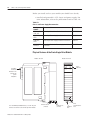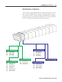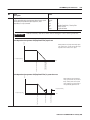
1
ControlLogix Drive
Module
1756-DMD30, 1756-DMF30
y
User Manual
Important User Information
Solid state equipment has operational characteristics differing from those of
electromechanical equipment. “Safety Guidelines for the Application,
Installation and Maintenance of Solid State Controls” (Publication SGI-1.1
available from your local Rockwell Automation Sales Office or online at
http://www.ab.com/manuals/gi) describes some important differences
between solid state equipment and hard-wired electromechanical devices.
Because of this difference, and also because of the wide variety of uses for
solid state equipment, all persons responsible for applying this equipment
must satisfy themselves that each intended application of this equipment is
acceptable.
In no event will Rockwell Automation, Inc. be responsible or liable for
indirect or consequential damages resulting from the use or application of
this equipment.
The examples and diagrams in this manual are included solely for
illustrative purposes. Because of the many variables and requirements
associated with any particular installation, Rockwell Automation, Inc.
cannot assume responsibility or liability for actual use based on the
examples and diagrams.
No patent liability is assumed by Rockwell Automation, Inc. with respect to
use of information, circuits, equipment, or software described in this
manual.
Reproduction of the contents of this manual, in whole or in part, without
written permission of Rockwell Automation, Inc. is prohibited.
Throughout this manual we use notes to make you aware of safety
considerations.
WARNING
!
ATTENTION
!
IMPORTANT
Identifies information about practices or
circumstances that can cause an explosion in a
hazardous environment, which may lead to personal
injury or death, property damage, or economic loss.
Identifies information about practices or
circumstances that can lead to personal injury or
death, property damage, or economic loss.
Identifies information that is critical for successful
application and understanding of the product.
Rockwell Automation
Support
Before you contact Rockwell Automation for technical assistance, we
suggest you please review the troubleshooting information contained
in this publication first.
If the problem persists, call your local Rockwell Automation
representative or contact Rockwell Automation in one of the
following ways:
Phone
Internet
United
States/Canada
1.262.512.8176
Outside United
States/Canada
You can access the phone number for your
country via the Internet:
1. Go to http://www.ab.com
2. Click on Product Support
(http://support.automation.rockwell.com)
3. Under Support Centers, click on Contact
Information
⇒
1. Go to http://www.ab.com
2. Click on Product Support
(http://support.automation.rockwell.com)
Your Questions or Comments on this Manual
If you find a problem with this manual, please notify us by using one
of these two methods:
• Filling out the enclosed "How Are We Doing" form
• Filling out the "Tell Us How We Can Make Our Manuals Better"
form online at
http://www.ab.com/manuals/dr/manuals_feedback.html
1
Important User Information . . . . . . . . . . . . . . . . . . . . . . . . 1-2
Rockwell Automation Support . . . . . . . . . . . . . . . . . . . . . . 1-3
Your Questions or Comments on this Manual . . . . . . . . 1-3
Summary of Changes
Preface
What is the ControlLogix Drive
Module?
Drive Comm (Drive
Communication)
Drive Module Features
Installing the Drive Module
Who Should Use This Manual . . . . . . . . . . . . . . . . . . . . . . P-1
Purpose of This Manual. . . . . . . . . . . . . . . . . . . . . . . . . . . P-1
What This Manual Contains . . . . . . . . . . . . . . . . . . . . . . . . P-2
Related Products and Documentation. . . . . . . . . . . . . . . . . P-2
What is the ControlLogix
Drive Module?. . . . . . . . . . . . . . . . . . . . . . . . . . . . . . . . . . 1-1
What Are Some of the Features Available On the ControlLogix
Drive Module? . . . . . . . . . . . . . . . . . . . . . . . . . . . . . . . 1-2
Connecting the Drive Module to SynchLink and Drive Comm . .
1-3
SynchLink . . . . . . . . . . . . . . . . . . . . . . . . . . . . . . . . . . 1-3
Drive Comm (Drive Communication) . . . . . . . . . . . . . . 1-3
Physical Features of the ControlLogix Drive Module . . . 1-4
Using Module Identification and Status Information . . . . . . 1-5
Preventing Electrostatic Discharge . . . . . . . . . . . . . . . . . . . 1-7
Removal and Insertion Under Power . . . . . . . . . . . . . . . . . 1-7
Chapter Summary and What’s Next . . . . . . . . . . . . . . . . . . 1-8
Interface to DPS Drive Equipment . . . . . . . . . . . . . . . . . . . 2-1
Drive Communication Protocol . . . . . . . . . . . . . . . . . . . . . 2-1
Initialization . . . . . . . . . . . . . . . . . . . . . . . . . . . . . . . . . . . 2-2
Synchronized Communication . . . . . . . . . . . . . . . . . . . . . . 2-2
Timing . . . . . . . . . . . . . . . . . . . . . . . . . . . . . . . . . . . . 2-2
Synchronization with CST. . . . . . . . . . . . . . . . . . . . . . . 2-3
Chapter Summary and What’s Next . . . . . . . . . . . . . . . . . . 2-3
General Module Features. . . . . . . . . . . . . . . . . . . . . . . . . . 3-1
Removal and Insertion Under Power (RIUP) . . . . . . . . . 3-2
Module Fault Reporting . . . . . . . . . . . . . . . . . . . . . . . . 3-2
Fully Software Configurable . . . . . . . . . . . . . . . . . . . . . 3-3
LED Status Information . . . . . . . . . . . . . . . . . . . . . . . . 3-3
Class I Division 2 Certification . . . . . . . . . . . . . . . . . . . 3-4
Agency Certification . . . . . . . . . . . . . . . . . . . . . . . . . . . 3-4
Configurable Module Features . . . . . . . . . . . . . . . . . . . . . . 3-4
Controller Communication Format . . . . . . . . . . . . . . . . 3-5
SynchLink Communications Format . . . . . . . . . . . . . . . 3-5
Module-Defined Data Tags. . . . . . . . . . . . . . . . . . . . . . 3-7
Electronic Keying. . . . . . . . . . . . . . . . . . . . . . . . . . . . . 3-8
Requested Packet Interval . . . . . . . . . . . . . . . . . . . . . . 3-10
Chapter Summary and What’s Next . . . . . . . . . . . . . . . . . . 3-10
Noting the Power Requirements . . . . . . . . . . . . . . . . . . . . 4-1
Installing the Module . . . . . . . . . . . . . . . . . . . . . . . . . . . . 4-2
Connecting SynchLink Cables . . . . . . . . . . . . . . . . . . . . . . 4-3
Connecting (Drive Comm Drive Communication) Cables . . 4-5
Publication 1756-UM522B-EN-P - February 2003
2
Removing the Module . . . . . . . . . . . . . . . . . . . . . . . . . . . . 4-6
Chapter Summary and What’s Next . . . . . . . . . . . . . . . . . . 4-7
Overview of the Configuration Process . . . . . . . . . . . . . . . 5-1
Configuring the Drive Module
Planning the System . . . . . . . . . . . . . . . . . . . . . . . . . . . . . 5-2
Understanding the Controller - Drive Module Interface . 5-2
Choosing the SynchLink Communication Formats . . . . . 5-2
Choosing the SynchLink Network Topology . . . . . . . . . 5-4
Checking and Updating the DriveExecutive Database . . . . . 5-6
Checking the DriveExecutive Database . . . . . . . . . . . . . 5-6
Checking the DriveExecutive Database (continued). . . . 5-7
Updating the DriveExecutive Database . . . . . . . . . . . . . 5-8
Using RSLogix 5000 to Configure the Drive Module . . . . . . 5-9
Using DriveExecutive to Configure Drive Module . . . . . . . . 5-16
Return to RSLogix 5000 to Finish Configuring the Drive Module
5-23
Chapter Summary and What’s Next . . . . . . . . . . . . . . . . . . 5-24
Troubleshooting the Drive Module Using the Status Indicators . . . . . . . . . . . . . . . . . . . . . . . . 6-1
Using DriveExecutive to Troubleshoot the Module . . . . . . . 6-3
Warning Signal on Main Screen . . . . . . . . . . . . . . . . . . 6-3
Fault and Alarm Window . . . . . . . . . . . . . . . . . . . . . . . 6-4
Fault and Alarm Window (continued) . . . . . . . . . . . . . . 6-5
Fault and Alarm Window (continued) . . . . . . . . . . . . . . 6-6
Diagnostic Parameters . . . . . . . . . . . . . . . . . . . . . . . . . 6-6
Diagnostic Parameters (continued) . . . . . . . . . . . . . . . . 6-7
Using RSLogix 5000 to Troubleshoot the Module . . . . . . . . 6-8
Warning Signal on Main Screen . . . . . . . . . . . . . . . . . . 6-8
Module Properties Window . . . . . . . . . . . . . . . . . . . . . 6-9
Chapter Summary and What’s Next . . . . . . . . . . . . . . . . . . 6-10
Module Specifications . . . . . . . . . . . . . . . . . . . . . . . . . . . . A-1
Specifications
Communication Specifications . . . . . . . . . . . . . . . . . . . . . . A-1
1756-DMD30 Specific Information Control Block Diagrams . . . . . . . . . . . . . . . . . . . . . . . . . . B-2
Overview . . . . . . . . . . . . . . . . . . . . . . . . . . . . . . . . . . B-2
Speed Control - Reference . . . . . . . . . . . . . . . . . . . . . . B-3
Speed Control - Regulator . . . . . . . . . . . . . . . . . . . . . . B-4
Process Control . . . . . . . . . . . . . . . . . . . . . . . . . . . . . . B-5
Position Control - Interpolated/Direct . . . . . . . . . . . . . . B-6
Position Control - Point to Point . . . . . . . . . . . . . . . . . B-7
Position Control - Auxiliary . . . . . . . . . . . . . . . . . . . . . B-8
Torque Control . . . . . . . . . . . . . . . . . . . . . . . . . . . . . . B-9
Speed / Position Feedback . . . . . . . . . . . . . . . . . . . . . B-10
Peak Detector / Control Logix . . . . . . . . . . . . . . . . . . B-11
Field Economy. . . . . . . . . . . . . . . . . . . . . . . . . . . . . . B-12
Parameters . . . . . . . . . . . . . . . . . . . . . . . . . . . . . . . . . . . B-13
How Parameters are Organized . . . . . . . . . . . . . . . . . B-15
Parameter Data In Linear List Format . . . . . . . . . . . . . B-24
Parameter Cross Reference By Name . . . . . . . . . . . . B-153
Publication 1756-UM522B-EN-P - February 2003
3
1756-DMF30 Specific Information
Interpretting Drive Module Faults in DriveExecutive .
Parameter 169 [Drive I/O Status] . . . . . . . . . . . . .
Parameter 323 [Fault Status 1] . . . . . . . . . . . . . . .
Parameter 324 [Fault Status 2] . . . . . . . . . . . . . . .
Parameter 326 [Alarm Status 1] . . . . . . . . . . . . . .
Parameter 327 [Alarm Status 2] . . . . . . . . . . . . . .
Parameter 1229 [SL Error Status] . . . . . . . . . . . . .
Parameter 2044 [Rail Port 0 Faults] . . . . . . . . . . .
Parameter 2050 [Rail Port 1 Faults] . . . . . . . . . . .
Parameter 2122 [MC Faults]. . . . . . . . . . . . . . . . .
Parameter 2123 [MC Warnings] . . . . . . . . . . . . . .
Parameter 2124 [Pwr Device Status] . . . . . . . . . .
Parameter 2125 [Interlock Code] . . . . . . . . . . . . .
Control Block Diagrams . . . . . . . . . . . . . . . . . . . . .
Current Control . . . . . . . . . . . . . . . . . . . . . . . . .
Speed Feedback . . . . . . . . . . . . . . . . . . . . . . . .
Peak Detector/Control Logic. . . . . . . . . . . . . . . .
Parameters . . . . . . . . . . . . . . . . . . . . . . . . . . . . . . .
How Parameters Are Organized . . . . . . . . . . . . .
Parameter Data In Linear List Format . . . . . . . . .
Interpretting Drive Module Faults in DriveExecutive .
Parameter 323 [Fault Status 1] . . . . . . . . . . . . . . .
Parameter 324 [Fault Status 2] . . . . . . . . . . . . . . .
Parameter 326 [Alarm Status 1] . . . . . . . . . . . . . .
Parameter 327 [Alarm Status 2] . . . . . . . . . . . . . .
Parameter 1229 [SL Error Status] . . . . . . . . . . . . .
Parameter 2044 [Rail Port 0 Faults] . . . . . . . . . . .
Parameter 2050 [Rail Port 1 Faults] . . . . . . . . . . .
Parameter 2122 [MC Faults]. . . . . . . . . . . . . . . . .
Parameter 2123 [MC Warnings] . . . . . . . . . . . . . .
Parameter 2124 [Pwr Device Status] . . . . . . . . . .
Parameter 2125 [Interlock Code] . . . . . . . . . . . . .
.
.
.
.
.
.
.
.
.
.
.
.
.
.
.
.
.
.
.
.
.
.
.
.
.
.
.
.
.
.
.
.
.
.
.
.
.
.
.
.
.
.
.
.
.
.
.
.
.
.
.
.
.
.
.
.
.
.
.
.
.
.
.
.
.
.
.
.
.
.
.
.
.
.
.
.
.
.
.
.
.
.
.
.
.
.
.
.
.
.
.
.
.
.
.
.
B-159
B-159
B-160
B-161
B-162
B-162
B-163
B-164
B-165
B-166
B-167
B-169
B-170
. . C-2
. . C-2
. . C-3
. . C-4
. . C-5
. . C-7
. C-14
C-100
C-100
C-101
C-102
C-102
C-103
C-104
C-105
C-106
C-107
C-108
C-109
Index
Publication 1756-UM522B-EN-P - February 2003
4
Publication 1756-UM522B-EN-P - February 2003
Summary of Changes
The table below summarizes the changes to this publication since the
last update:
1
For this updated information:
See:
Reliability specification
A-1
Documentation of 1756-DMD30 (Firmware Revision 2.01) Algorithms,
Parameters and Faults
B-1
Documentation of 1756-DMF30 (Firmware Revision 1.09) Algorithms,
Parameters and Faults
C-1
Publication 1756-UM522B-EN-P - February 2003
Summary of Changes
2
Notes:
Publication 1756-UM522B-EN-P - February 2003
Preface
About This Preface
This preface describes how to use this manual. The following table
describes what this preface contains and its location.
For information about:
Who Should Use This
Manual
See page:
Who Should Use This Manual
Preface-1
Purpose of This Manual
Preface-1
Related Products and Documentation
Preface-2
You must be able to program and operate an Allen-Bradley
ControlLogix™ Logix controller and ControlLogix I/O modules to
efficiently use your Drive module.
We assume that you know how to do this in this manual. If you do
not, refer to Related Documentation, before you attempt to use this
module.
IMPORTANT
SynchLink must be used in conjunction with a standard
control network, such as ControlNet or Ethernet. A
standard network is used for general control interlocking
and transfer of diagnostic data across the system.
SynchLinkdoesnotfunctionasastandardcontrolnetwork
(e.g. it broadcasts data in a unidirectional manner).
Purpose of This Manual
1
This manual describes how to install, configure, and troubleshoot
your ControlLogix Drive module.
Publication 1756-UM522B-EN-P - February 2003
Preface
2
What This Manual Contains
This user manual contains the following sections:
•
•
•
•
•
•
•
•
Related Products and
Documentation
Description of the Drive module
Description of Drive Communication
Description of Drive module certifications and features
Description of how to install the Drive module and connect the
fiber optic cables
Description of how to configure the Drive module with RSLogix
5000 and DriveExecutive programming software
Description of how to troubleshoot the Drive module
Listing of Drive module specifications
Information specific to the SD3000 Interface (1756-DMD30)
The following table lists related Allen-Bradley products and
documentation:
Table Preface.A
Related Documentation
Publication 1756-UM522B-EN-P - February 2003
Catalog
number:
Document title:
Pub. number:
1756-DM
ControlLogix Drive Module Installation Instructions
1756-IN577
1756-A4, -A7,
-A10, -A13
ControlLogix Chassis Installation Instructions
1756-IN080B
1756-PA72,
-PB72
ControlLogix Power Supply Installation Instructions
1756-5.67
1756-PA75,
-PB75
ControlLogix Power Supply Installation Instructions
1756-5.78
1756-Series
ControlLogix Module Installation Instructions
(Each module has separate installation document.)
Multiple 1756-IN
numbers
1756-Series
ControlLogix System User Manual
1756-UM001
Multiple
numbers
SynchLink Design Guide
1756-TD008
1751-SLBA
SynchLink Base Block Installation Instructions
1751-IN001
1751-SL4SP
SynchLink 4-port Splitter Block Installation
Instructions
1751-IN002
1751-SLBP
SynchLink Bypass Switch Block Installation
Instructions
1751-IN003
PowerFlex
700S
PowerFlex 700S User Manual
20D-UM001
Preface
3
The following table lists related Reliance Electric products and
documentation:
Table Preface.B
Related Documentation
Catalog
number:
Document title:
Pub. number:
Multiple
numbers
Distributed Power System Overview
S-3005
SD3000,
SF3000
Distributed Power System
SD3000/SF3000
Power Module Interface Rack and Modules
S-3008
SD3000
Distributed Power System
SD3000 Drive
Diagnostics, Troubleshooting, and Start-Up Guidelines
S-3011
SD3000,
SF3000
Distributed Power System
SD3000/SF3000
3-Phase DC Power Models
S-3037
SD3000
Distributed Power System
High Horsepower D-C Power Bridge
1000 HP Power Modules
S-3039
SF3000
Distributed Power System
SF3000 Panel-Mounted
Single-Phase Field Power Modules
S-3060
SD3000,
SF3000
Distributed Power System
SD3000/SF3000
Parallel Gate Amplifier System
S-3045
If you need more information on these products, contact your local
Allen-Bradley integrator or sales office for assistance. Information and
manuals are also available online at http://www.ab.com/manuals/ and
http://www.theautomationbookstore.com/.
Publication 1756-UM522B-EN-P - February 2003
Preface
4
Notes:
Publication 1756-UM522B-EN-P - February 2003
Chapter
1
What is the ControlLogix Drive Module?
This chapter describes the ControlLogix Drive module. It also
describes what you must know and do before using the Drive
module.
For information about:
What is the ControlLogix
Drive Module?
See page:
What is the ControlLogix Drive Module?
1-1
Connecting the Drive Module to SynchLink
and Drive Comm
1-3
Using Module Identification and Status
Information
1-5
Preventing Electrostatic Discharge
1-7
Removal and Insertion Under Power
1-7
Chapter Summary and What’s Next
1-8
The 1756-DM Drive Module is a single slot ControlLogix based
module for interface to Reliance Electric Distributed Power System
(DPS) drive equipment. Each drive module interfaces with an
individual Power Module Interface (PMI) chassis, performing velocity
and position and outer torque control.
Figure 1.1 SD3000 System Example
ControlLogix Chassis
with Drive Module
Drive Communication
1
Motor with
resolver
DPS with PMI
Chassis
Publication 1756-UM522B-EN-P - February 2003
1-2
What is the ControlLogix Drive Module?
There are two types of Drive module, each works with a different
type of DPS drive equipment.
Table 1.A
Drive Module
DPS Equipment
Description
1756-DMD30
SD3000 6 Pulse
DC Drive S6 and S6R
SD3000 12 Pulse
DC Drive S12 and S12R
SF3000
Three Phase Field Supply
1756-DMF30
What Are Some of the Features Available On the ControlLogix
Drive Module?
The following are some of the features available on the ControlLogix
Drive module:
• The 1756-DMD30 utilizes velocity and position and outer torque
control similar to the PowerFlex 700S
• Motor Control capability mimics the respective Reliance Electric
Distributed Power drive
• PC Tools, such as RSLogix 5000TM and DriveExecutiveTM in the
DriveTools 2000TM program suite, used for programming,
configuring, monitoring and troubleshooting
• Fiber optic connection to the Power Module Interface
• SynchLinkTM for advanced high performance synchronization
and data transfer.
• Removal and insertion under power (RIUP) - This system feature
allows you to remove and insert the module while power is
applied. For more information on RIUP, see page 1-7.
• Class I Division 2, UL, CSA, and CE Agency Certification
Publication 1756-UM522B-EN-P - February 2003
What is the ControlLogix Drive Module?
Connecting the Drive
Module to SynchLink and
Drive Comm
1-3
SynchLink
The ControlLogix Drive module mounts in a ControlLogix chassis and
connects to other SynchLink nodes through a fiber optic cable system.
Table 1.B
Fiber Optic Cables for SynchLink
Catalog Number:
Cable Length
Cables per box:
1403-CF001
1 meter
2
1403-CF003
3 meters
2
1403-CF005
5 meters
2
1403-CF010
10 meters
1
1403-CF020
20 meters
1
1403-CF050
50 meters
1
1403-CF100
100 meters
1
1403-CF250
250 meters
1
Drive Comm (Drive Communication)
The ControlLogix Drive module connects to a PMI chassis through
special Drive Communication fiber optic cables.
Table 1.C
Fiber Optic Cables for Drive Communication
Catalog Number
Length
1756-DMCF001
1 meter
1756-DMCF003
3 meters
1756-DMCF010
10 meters
1756-DMCF030
30 meters
(1)
N/A
1756-DMAF
(1)
Use the 1756-DMAF to connect existing UDC/PMI fiber optic cables to the Drive Module
Publication 1756-UM522B-EN-P - February 2003
1-4
What is the ControlLogix Drive Module?
Before you install and use your module you should have already:
• installed and grounded a 1756 chassis and power supply. For
more information, refer to the publications listed in Table 1.D.
Table 1.D
Chassis and Power Supply Documentation
Catalog
number:
Document title:
Pub. number:
1756-A4, -A7,
-A10, -A13
ControlLogix Chassis Installation Instructions
1756-IN080
1756-PA72,
-PB72
ControlLogix Power Supply Installation Instructions
1756-5.67
1756-PA75,
-PB75
ControlLogix Power Supply Installation Instructions
1756-5.78
1756-PA75R/A,
-PB75R/A
ControlLogix Redundant Power Supply Installation
Instructions
1756-IN573
Physical Features of the ControlLogix Drive Module
Module side view
Module front view
SD3000 INTERFACE
ControlBus
ConnectorInterface to the
ControlLogix
system
backplane
LINK
COMM
LINK
SYNC
DRIVE
COMM OK
DRIVE
FAULT
OS OK
Status
Indicators
OK
Tx (rear)
Rx (front)
The 1756-DMD30, SD3000 Interface, is shown. Physical
features are common to all ControlLogix Drive Modules.
Publication 1756-UM522B-EN-P - February 2003
Transmit Ports
(in back)
Receive Ports
(in front)
SynchLink
Ports
Drive
Communication
Ports
What is the ControlLogix Drive Module?
1-5
Backplane Connector - The backplane connector connects the
module to the ControlLogix chassis backplane.
Status Indicators - The status indicators display the module’s
communications, Drive Communication and SynchLink system status.
SynchLink Transmit Fiber Port - The transmit fiber port allows
connection (via fiber optic cables) to other SynchLink modules so the
module can send data.
SynchLink Receive Fiber Port - The receive fiber port allows
connection (via fiber optic cables) to other SynchLink modules so the
module can receive data.
Drive Communication Transmit Fiber Port - The transmit fiber
port allows connection (via fiber optic cables) to the PMI processor of
the drive.
Drive Communication Receive Fiber Port - The receive fiber port
allows connection (via fiber optic cables) to the PMI processor of the
drive.
Using Module Identification
and Status Information
Each ControlLogix Drive module maintains specific identification
information that separates it from all other modules. This information
assists you in tracking all the components of your system.
For example, you can track module identification information to be
aware of exactly what modules are located in any ControlLogix rack
at any time. While retrieving module identity, you can also retrieve
the module’s status.
Each module maintains the following information:
Table 1.E
Module Identification and Status Information
Module Identification:
Description:
Product Type
Module’s product type, such as Digital I/O or
Analog I/O module
Catalog Code
Module’s catalog number
Major Revision
Module’s major firmware revision number
Minor Revision
Module’s minor firmware revision number
Publication 1756-UM522B-EN-P - February 2003
1-6
What is the ControlLogix Drive Module?
Table 1.E
Module Identification and Status Information
Module Identification:
Description:
Status
Module’s status. Returns the following information:
• Controller ownership (if any)
• Whether module has been configured
• Device Specific Status, such as:
– Self-Test
– Flash update in progress
– Communications fault
– Not owned (outputs in program mode)
– Internal fault (need flash update)
– Run mode
• Minor recoverable fault
• Minor unrecoverable fault
• Major recoverable fault
• Major unrecoverable fault
Vendor ID
Module manufacturer vendor, for example Allen-Bradley
Serial Number
Module serial number
Length of ASCII Text String
Number of characters in module’s text string
ASCII Text String
Module name
IMPORTANT
Publication 1756-UM522B-EN-P - February 2003
To retrieve this information, you can use the WHO
service in the RSLinx software. For more information
on how to retrieve module identification information,
see the RSLinx online help.
What is the ControlLogix Drive Module?
Preventing Electrostatic
Discharge
This module is sensitive to electrostatic discharge.
ATTENTION
!
Removal and Insertion
Under Power
1-7
Preventing Electrostatic Discharge
This equipment is sensitive to electrostatic discharge,
which can cause internal damage and affect normal
operation. Follow these guidelines when you handle
this equipment:
• Touch a grounded object to discharge potential
static.
• Wear an approved grounding wrist strap.
• Do not touch connectors or pins on component
boards.
• Do not touch circuit components inside the
equipment.
• If available, use a static-safe workstation.
• When not in use, store the equipment in
appropriate static-safe packaging.
These modules are designed to be installed or removed while chassis
power is applied, while in non-hazardous locations only.
WARNING
!
ATTENTION
!
IMPORTANT
When you insert or remove the module while
backplane power is on, an electrical arc can occur.
This could cause an explosion in hazardous location
installations. Be sure that power is removed or the
area is nonhazardous before proceeding.
The removal of a Drive Module while under power
may cause personal injury or property damage. Make
sure that removal of the module does not adversely
impact other parts of the system.
Repeated electrical arcing causes excessive wear to
contacts on both the module and its mating
connector. Worn contacts may create electrical
resistance that can affect module operation.
Publication 1756-UM522B-EN-P - February 2003
1-8
What is the ControlLogix Drive Module?
Chapter Summary and
What’s Next
Publication 1756-UM522B-EN-P - February 2003
In this chapter, you learned about the ControlLogix Drive module.
Move to Chapter 2, Drive Comm (Drive Communication) for details
on the communications interface to DPS equipment.
Chapter
2
Drive Comm (Drive Communication)
This chapter describes Drive Comm (Drive Communication), the
interface between the ControlLogix Drive module communicates and
Distributed Power System (DPS).
For information about:
Interface to DPS Drive
Equipment
See page:
Interface to DPS Drive Equipment
2-1
Drive Communication Protocol
2-1
Initialization
2-2
Synchronized Communication
2-2
Chapter Summary and What’s Next
2-3
The main function of the Drive module is to interface to Distributed
Power System (DPS) drive equipment, enabling a ControlLogix
processor to control the drive equipment. A ControlLogix processor
performs high level control algorithms and drive coordination. The
Drive module performs outer control loop processing(1), and the
Power Module Interface (PMI) performs real-time control of the
Power Module.
Each drive module interfaces with an individual Power Module
Interface (PMI) processor. It resides in a ControlLogix chassis and
connects to a PMI processor via fiber-optic and Drive Communication
protocol.
Drive Communication
Protocol
Drive Communication is a point to point serial link between the Drive
module and the Power Module Interface (PMI), on fiber-optic cable. It
is similar to the protocol used between the Universal Drive Controller
(UDC) and the PMI processor in an AutoMax DPS environment. The
data is Manchester-encoded and transmitted over the fiber-optic links
at a rate of 10M bits per second. Transfers on fiber-optic cables are
immune to electromagnetic interference (EMI).
During initialization, the Drive Module and PMI processor use an
asynchronous master-slave protocol to transfer the PMI operating
system to the PMI processor and to establish synchronized
communication. After initialization, they use synchronized “Set
(1)
1
The 1756-DMF30 does not perform outer control loop processing - it only functions as a bridge between the
ControlLogix controller and the PMI processor.
Publication 1756-UM522B-EN-P - February 2003
2-2
Drive Comm (Drive Communication)
Point/Feedback Data Exchange” to transfer data. The Drive Module
sends set point data to the PMI processor, which returns feedback
data to the Drive Module.
Initialization
At boot time, the Drive Module and PMI processor use an
asynchronous master-slave protocol to transfer the PMI operating
system and establish synchronized communication. The PMI
processor is the master, and commences by requesting its operating
system. The Drive Module responds by downloading the operating
system in a special message, containing up to 256 byte packets.
When the operating system transfer is complete, the Drive Module
sends a configuration message and a gain message. The configuration
message contains information that fixes the communication frequency
at 4 mS. Once the Drive Module and PMI processor have
synchronized communications, normal Set Point/Feedback data
transfer can begin.
Synchronized
Communication
The synchronized protocol is called “Set Point/Feedback Data
Exchange”. The drive module sends set point data to the PMI
processor. The set point data contains reference data, for drive
control, and a time stamp. This time stamp enables the PMI processor
to calculate what the proper time is for the next feedback message.
The PMI processor sends feedback messages to the Drive Module.
The feedback messages contains data about drive operation.
Timing
The velocity loop updates (reads from, and writes to Drive
Communication) every 2 mS. After every other velocity loop update
(at a 4 mS interval), the position loop performs its update. After every
position update, the Drive Module sends set point data to the PMI
processor. After the next velocity update (but before the following
one), the PMI processor sends feedback data to the Drive Module.
Refer to the following timing chart.
Publication 1756-UM522B-EN-P - February 2003
Drive Comm (Drive Communication)
2-3
Figure 2.1 Drive Communication Timing
Velocity Loop Update
Position Loop Update
Set Point Data to PMI
Feedback Data
to Drive Module
4 mS
Synchronization with CST
Synchronization to Coordinated System Time (CST) is not necessary to
synchronize Drive Communication between the Drive Module and the
PMI processor. However, if the Drive Module is synchronized to the
CST, Drive Communication will also synchronize to the CST.
Chapter Summary and
What’s Next
In this chapter, you learned about Drive Communication. For more
information on Drive Module features see Chapter 3, Drive Module
Features.
Publication 1756-UM522B-EN-P - February 2003
2-4
Drive Comm (Drive Communication)
Notes:
Publication 1756-UM522B-EN-P - February 2003
Chapter
3
Drive Module Features
This chapter describes the ControlLogix Drive module features.
For information about:
See page:
General Module Features
3-1
Configurable Module Features
3-4
Chapter Summary and What’s Next
3-10
General module features are features (e.g. Removal and Insertion
Under Power) that are supported on the module regardless of
configuration and application.
Configurable module features are features (e.g. Communications
Format) that can be configured to work differently in various
applications.
General Module Features
The following general module features are available with the
ControlLogix Drive module:
•
•
•
•
•
•
1
Removal and Insertion Under Power (RIUP)
Module Fault Reporting
Fully Software Configurable
LED Status Information
Class I Division 2 Certification
Agency Certification
Publication 1756-UM522B-EN-P - February 2003
3-2
Drive Module Features
Removal and Insertion Under Power (RIUP)
All ControlLogix Drive modules may be removed and inserted from
the chassis while power is applied. This feature allows greater
availability of the overall control system because, while the module is
being removed or inserted, there is no additional disruption to the rest
of the controlled process.
WARNING
!
ATTENTION
!
IMPORTANT
When you insert or remove the module while
backplane power is on, an electrical arc can occur.
This could cause an explosion in hazardous location
installations. Be sure that power is removed or the
area is nonhazardous before proceeding.
The removal of a Drive Module while under power
may cause personal injury or property damage. Make
sure that removal of the module does not adversely
impact other parts of the system.
Repeated electrical arcing causes excessive wear to
contacts on both the module and its mating
connector. Worn contacts may create electrical
resistance that can affect module operation.
Module Fault Reporting
ControlLogix Drive modules provide both hardware and software
indication when a module fault has occurred. Each module’s LED fault
indicator as well as DriveExecutive and RSLogix 5000 will graphically
display this fault and include a fault message describing the nature of
the fault.
This feature allows you to determine how your module has been
affected and what action should be taken to resume normal
operation.
Publication 1756-UM522B-EN-P - February 2003
Drive Module Features
3-3
Fully Software Configurable
RSLogix 5000 and DriveExecutive software packages use custom,
easily understood interfaces to determine the module configuration.
All module features are enabled or disabled through the configuration
portions of the software.
You can also use the software to interrogate any module in the system
to retrieve
•
•
•
•
•
serial number
revision information
catalog number
vendor identification
error/fault information
By eliminating such tasks as setting hardware switches and jumpers,
the software makes module configuration easier.
LED Status Information
The ControlLogix Drive module has LED indicators on the front of the
module that allow you to check the module health and operational
status.
The following status can be checked with the LED indicators:
•
•
•
•
SynchLink and ControlLogix backplane status
Drive Comm status
Drive status
Module health status
For examples of LED indicators, see page 6-1.
Publication 1756-UM522B-EN-P - February 2003
3-4
Drive Module Features
Class I Division 2 Certification
The ControlLogix Drive module is certified for use in nonhazardous
locations as well as Class I, Division 2 hazardous Locations containing
gas groups A, B, C, and D. This equipment may be used as a
component of a control system which is certified to operate in
hazardous locations.
WARNING
!
ATTENTION
!
When you insert or remove the module while
backplane power is on, an electrical arc can occur.
This could cause an explosion in hazardous location
installations. Be sure that power is removed or the
area is nonhazardous before proceeding.
The removal of a Drive Module while under power
may cause personal injury or property damage. Make
sure that removal of the module does not adversely
impact other parts of the system.
Agency Certification
When the Drive module is marked appropriately, the following
agency certifications apply:
• UL Listed Industrial Control Equipment
• CSA Certified Process Control Equipment
• CSA Certified for Class I, Division 2 Hazardous Locations
Configurable Module
Features
The following Drive module features are configurable via RSLogix
5000 and DriveExecutive:
•
•
•
•
•
•
Publication 1756-UM522B-EN-P - February 2003
Controller Communication Format
SynchLink Controller Communication Format
Electronic Keying
Requested Packet Interval
Transmitted Direct Words
SynchLink Mastership
Drive Module Features
3-5
Each of these features is described in this section, including
information on which RSLogix 5000 and DriveExecutive configuration
screens should be used to configure the feature. For an overview of
the entire configuration process, see Chapter 5, Configuring the Drive
Module.
Controller Communication Format
The controller communications format defines the connection
between the owner-controller and the module (i.e. determines what
type of data is transferred between them). The 1756-DMD30 module
supports Velocity Control, Position Control, User-Defined and Custom
User-Defined communication formats. The 1756-DMF30 supports the
User-Defined communication format.
SynchLink Communications Format
The SynchLink communications format defines the connection at the
SynchLink Receive Port and the SynchLink Transmit Port. It
determines the type and number of data type in each connection.
SynchLink messages are structured as six 32-bit words; the words are
divided into three types:
• Direct - Data delivered in a single message. A SynchLink
message can contain a maximum of four direct data words; each
word is 32 bits in length. Direct data can be automatically
forwarded to the next node in the daisy chain and ring
configurations.
• Buffered - Data that exceeds the four word limit of a direct data
transfer. A maximum of 18 buffered are transfered every 500µS.
Buffered data is appropriately segmented at the transmitting
module and reassembled at the receiving module. Buffered data
cannot be automatically forwarded to the next node in the daisy
chain and ring configurations.
• Axis - the Drive module does not support this data type.
Multiple Port Communications Formats in Single Module
You must set a communications format for receiving data (Receive
Port Communications Format) and transmitting data (Transmit Port
Communications Format) in each SynchLink node.
Publication 1756-UM522B-EN-P - February 2003
3-6
Drive Module Features
The following requirements apply to communication format choices:
• If a Drive module does not receive data (e.g. the first node in a
daisy chain topology), you must choose the No Receive Data
Receive Port communication format.
• If a Drive module does not transmit data (e.g. an end node), you
must choose the No Transmit Data Transmit Port
communications format.
• The receive communication format for any Drive module that
receives data must match the transmit communications format of
the upstream node in the system.
IMPORTANT
The receive and transmit on the same module do not have
to match.
Also, once the module is created, the communications
format cannot be changed. The module must be deleted
and recreated.
Internal Scan on Drive Module
Every 500µS, the Drive module scans its internal hardware and
captures a “snapshot” of the data there. This data is then sent to the
local owner-controller at the Change of State (COS) instance,
independent of the requested packet interval (RPI) rate. But,
depending on the communications formats chosen during module
configuration, data types are transmitted between SynchLink nodes
(via the fiber optic cable) at various rates and may be transmitted
multiple times between the 500µS snapshots.
IMPORTANT
The transfer rate times listed in Table 3.A and
Table 3.B only represent the rate at which data is
passed between SynchLink modules over the fiber
optic cable.
Although the data is passed over the fiber optic cable
at various rates, depending on the communications
format choices, the owner-controllers in each local
chassis only receive the data after the local
SynchLink module’s internal scan every 500µS.
The Drive module updates its receive and transmit buffers once every
500µS. Because direct data can be passed through from node to node
once every 50µS, up to 10 nodes can be updated with direct data in a
single 500µS SynchLink scan. Pass-through functionality only applies
Publication 1756-UM522B-EN-P - February 2003
Drive Module Features
3-7
to direct data in a daisy chain configuration, In order to pass-through
buffered data, the local controller must intervene to move data along.
Table 3.A
Drive Module Receive Communications Formats
Receive Port Communications Format
Transfer Rate (across the fiber optic
cable) for Each Data Type:
2 Direct Words, 18 Buffered
Direct Data - Updated every 50µS
Buffered Data - Updated every 250µS
4 Direct Words, 18 Buffered
Direct Data - Updated every 50µS
Buffered Data - Updated every 500µS
4 Direct Words, 8 Buffered
Direct Data - Updated every 50µS
Buffered Data - Updated every 250µS
No Receive Data
No data updated in this format
Table 3.B
Drive Module Transmit Communications Formats
Transmit Port Communications Format
Transfer Rate (across the fiber optic
cable) for Each Data Type:
2 Direct Words, 18 Buffered
Direct Data - Updated every 50µS
Buffered Data - Updated every 250µS
4 Direct Words, 18 Buffered
Direct Data - Updated every 50µS
Buffered Data - Updated every 500µS
4 Direct Words, 8 Buffered
Direct Data - Updated every 50µS
Buffered Data - Updated every 250µS
Listen Only, No Transmit Data
No data updated in this format
No Transmit Data
No data updated in this format
Module-Defined Data Tags
When you create a module, module-defined data types and tags are
created in the RSLogix 5000 programming software. These tags allow
you to access the Input and Output Data of the module via the
controller’s ladder logic, if necessary
The types of tags created vary, depending on which communications
format you choose when creating a module. There are two types of
tags:
• Input Data Tags
• Output Data Tags
Publication 1756-UM522B-EN-P - February 2003
3-8
Drive Module Features
Electronic Keying
Instead of plastic mechanical backplane keys, electronic keying
allows the ControlLogix system to control what modules belong in the
various slots of a configured system.
During module configuration, you must choose one of the following
keying options for your SynchLink module:
• Exact Match
• Compatible Match
• Disable Keying
When the controller attempts to connect to and configure a Drive
module (e.g. after program download), the module compares the
following parameters before allowing the connection and
configuration to be accepted:
•
•
•
•
•
Vendor
Product Type
Catalog Number
Major Revision
Minor Revision
The comparison is made between the keying information present in
the Drive module and the keying information in the controller’s
program. This feature can guard against the inadvertent operation of a
control system with the wrong module in the wrong slot.
Exact Match
All of the parameters listed above must match or the inserted module
will reject a connection to the controller.
Compatible Match
The Compatible Match mode allows a Drive module to determine
whether it can emulate the module defined in the configuration sent
from the controller.
With ControlLogix Drive modules, the module can emulate older
revisions. The module will accept the configuration if the controller’s
major.minor revision is less than or equal to the physical
module’s revision.
Publication 1756-UM522B-EN-P - February 2003
Drive Module Features
3-9
For example, if the configuration contains a major.minor revision of
2.7, the module inserted into the slot must have minor revision of 2.7
or higher for a connection to be made.
TIP
We recommend using Compatible Match whenever
possible. Remember, though, the module will only
work to the level of the configuration.
For example, if a slot is configured for a module
with major.minor revision of 2.7 and you insert a
module with a major.minor revision of 3.1, the
module works at the 2.7 level despite having been
previously upgraded.
If possible, we suggest you make sure configuration
is updated to match the revision levels of all Drive
modules. Failure to do so may not prevent the
application from working but may defeat the
purpose of upgrading your modules’ revision levels.
Disable Keying
The inserted module attempts to accept a connection to the controller
regardless of its type.
ATTENTION
!
Be extremely cautious when using the disable
keying option; if used incorrectly, this option can
lead to personal injury or death, property damage
or economic loss.
If keying is disabled, a controller makes a connection with most
modules of the same type as that used in the slot configuration.
A controller will not establish a connection if any of the following
conditions exist, even if keying is disabled:
• The slot is configured for one module type (e.g. digital input
module) and a module of another type (e.g. Drive module) is
inserted in the slot.
• The module inserted into the slot cannot accept some portion of
the configuration. This case should not arise if the slot is
configured for a Drive module and one is inserted.
Publication 1756-UM522B-EN-P - February 2003
3-10
Drive Module Features
Requested Packet Interval
The Requested Packet Interval (RPI) is a configurable parameter that
defines when the module multicasts its data onto the local chassis
backplane.
In addition to the RPI, Change of State (COS) functionality also causes
the module to produce its data to the consuming controller whenever
the values of the data changes. The RPI timer is asynchronous to the
COS functionality. Both cause the module to produce data when
triggered.
Buffered, Direct and Diagnostic Data - RPI Effect on Output Data (from the
controller)
As a producing controller writes data to the Drive module, the output
data is placed in a local buffer until the next RPI reset occurs. When
the RPI timer expires, the output data is moved from the controller’s
local buffer to the Drive module.
The RPI timer is asynchronous to the program execution. Therefore, a
worst case update to the Drive module can be calculated by adding
the program execution time to the RPI timer setting, as configured by
the user.
Chapter Summary and
What’s Next
Publication 1756-UM522B-EN-P - February 2003
In this chapter, you learned about the ControlLogix Drive module
features. Move to Chapter 4, Installing the Drive Module, to learn how
to install the module.
Chapter
4
Installing the Drive Module
This chapter describes how to install the ControlLogix
Drive module.
For information about:
Noting the Power
Requirements
See page:
Noting the Power Requirements
4-1
Installing the Module
4-2
Connecting SynchLink Cables
4-3
Connecting (Drive Comm Drive
Communication) Cables
4-5
Removing the Module
4-6
Chapter Summary and What’s Next
4-7
This module receives power from the 1756 chassis power supply and
requires 2 sources of power from the backplane:
• 1.35A at 5.1V dc
• 3.0mA at 24V dc
Account for this power consumption (6.96W) in addition to the
requirements of all other modules in the chassis to prevent
overloading the power supply.
1
Publication 1756-UM522B-EN-P - February 2003
4-2
Installing the Drive Module
Installing the Module
You can install or remove the module while chassis power is applied.
WARNING
!
ATTENTION
!
IMPORTANT
When you insert or remove the module while
backplane power is on, an electrical arc can occur.
This could cause an explosion in hazardous location
installations. Be sure that power is removed or the
area is nonhazardous before proceeding.
The removal of a Drive Module while under power
may cause personal injury or property damage. Make
sure that removal of the module does not adversely
impact other parts of the system.
Repeated electrical arcing causes excessive wear to
contacts on both the module and its mating
connector. Worn contacts may create electrical
resistance that can affect module operation.
1. Align the circuit board with the top and bottom chassis guides.
Printed
Circuit
Board
Publication 1756-UM522B-EN-P - February 2003
Installing the Drive Module
4-3
2. Slide the module into the chassis until the module locking
tabs ‘click’.
Locking tab
Connecting SynchLink
Cables
The two fiber optic ports on the bottom-left of the module are for
SynchLink. The front-left port is receives SynchLink data, and the
rear-left port is transmits SynchLink data.
ATTENTION
!
TIP
The Drive module is a Class I LED product. Light
levels may cause damage to eyesight. Do not look
directly into the fiber ports or fiber cables.
Keep the plugs that were removed to connect the
fiber optic cables. When the cables are disconnected,
you can reinsert the plugs into the ports to protect
them.
Publication 1756-UM522B-EN-P - February 2003
4-4
Installing the Drive Module
Figure 4.1 SynchLink Connections
Tx (rear)
Rx (front)
Tx Rx
Refer to See Table 1.B on page 1-3 for information on available
pre-configured fiber optic SynchLink cables.
Table 4.A lists the possible connections that might be made to your
1756-DM module and where to connect the fiber optic cable.
Table 4.A
Making Fiber Optic Cable Connections to the 1756-DM Module
Publication 1756-UM522B-EN-P - February 2003
If your 1756-DM module
is configured to:
Make this fiber optic cable connection:
transmit data only
Connect the fiber optic cable to the rear port. The other end
of the cable should be connected to a device receiving data
over the SynchLink from your 1756-DM module.
receive data only
Connect the fiber optic cable to the front port. The other end
of the cable should be connected to a device transmitting
data to your 1756-DM module over the SynchLink.
transmit and receive data
1. Connect the fiber optic cable going to (i.e. transmitting
the data to) a module receiving the data to the front port.
2. Connect the fiber optic cable coming from (i.e. receiving
the data from) a module transmitting data to the rear port.
Installing the Drive Module
Connecting (Drive Comm
Drive Communication)
Cables
4-5
The two fiber optic ports on the bottom-right of the module are for
Drive Comm. The front-right port receives data from the PMI
processor on the drive. The rear-right port transmits data to the PMI
processor.
• Connect the 1756-DM transmit port (Tx) to the PMI receive port
(RCV).
• Connect the 1756-DM receive port (Rx) to the PMI transmit port
(XMT). .
ATTENTION
!
TIP
The Drive module is a Class I LED product. Light
levels may cause damage to eyesight. Do not look
directly into the fiber ports or fiber cables.
Keep the plugs that were removed to connect the
fiber optic cables. When the cables are disconnected,
you can reinsert the plugs into the ports to protect
them.
Figure 4.2 Drive Comm - Drive Module End Connections
Tx (rear)
Rx (front)
Tx Rx
Publication 1756-UM522B-EN-P - February 2003
4-6
Installing the Drive Module
Figure 4.3 Drive Comm - PMI Processor Connections
C
O
M
M
T
XM
V
RC
Refer to See Table 1.C on page 1-3 for information on available
pre-configured fiber optic Drive Comm cables.
Removing the Module
ATTENTION
Before you remove the module, you must disconnect
the fiber optic cables.
!
1. Push in the top and bottom locking tabs.
TIP
If you kept the plugs that were removed to
connect the fiber optic cables, reinsert them to
protect the ports.
2. Pull the module out of the chassis as shown.
Publication 1756-UM522B-EN-P - February 2003
Installing the Drive Module
4-7
Figure 4.4
Locking tabs
Chapter Summary and
What’s Next
In this chapter, you learned how to install the ControlLogix Drive
module. Move to Chapter 5, Configuring the Drive Module, to learn
how to configure the module.
Publication 1756-UM522B-EN-P - February 2003
4-8
Installing the Drive Module
Notes:
Publication 1756-UM522B-EN-P - February 2003
Chapter
5
Configuring the Drive Module
This chapter describes how to configure the ControlLogix Drive
Module using RSLogix 5000 and DriveExecutive in the DriveTools
2000 programming suite.
For information about:
Overview of the
Configuration Process
See page:
Overview of the Configuration Process
5-1
Planning the System
5-2
Checking and Updating the DriveExecutive
Database
5-6
Using RSLogix 5000 to Configure the Drive
Module
5-9
Using DriveExecutive to Configure Drive
Module
5-16
Return to RSLogix 5000 to Finish
Configuring the Drive Module
5-23
Chapter Summary and What’s Next
5-24
To configure your ControlLogix Drive Module, you must perform the
following steps:
1. Plan the system.
• Choose Controller Communication format
• Choose SynchLink communications format (if you are using
SynchLink)
• Choose SynchLink topology (if you are using SynchLink)
2. Make sure DriveExecutive has database for the firmware
revision and configuration of the module.
3. Configure each Drive Module with RSLogix 5000.
4. Configure each Drive Module with DriveExecutive, and
download parameters and links to Drive module.
5. Return to RSLogix 5000, and download program to ControlLogix
processor.
1
Publication 1756-UM522B-EN-P - February 2003
5-2
Configuring the Drive Module
Planning the System
Before programming, you must choose a Controller - Drive Module
interface (Controller Communication Format) for each Drive Module
in the system.
If you are going to use SynchLink, you must choose the SynchLink
data format, and a SynchLink network topology. This chapter covers
these topics.
Understanding the Controller - Drive Module Interface
You must configure communications between the ControlLogix
controller and the Drive Module by selecting a “Controller
Communication Format”. A controller communication format is a set
of links that connects controller output tags to Drive Module sinking
parameters, and connects controller input tags to Drive Module
sourcing parameters. There are four controller communication formats
to choose from, depending on which module you are configuring:
•
•
•
•
Velocity Control
Position Control
User-Defined Control
Custom User-Defined Control
Each controller communication format contains both required
connections and user definable connections. You must use both
RSLogix 5000 and DriveExecutive to configure these connections. The
programming software will not allow you to choose Velocity Control
or Position control for the 1756-DMF30.
IMPORTANT
Once the module is created, the communications
format cannot be changed. The module must be
deleted and recreated.
Choosing the SynchLink Communication Formats
You must set a communications format for receiving data (Receive
Port Communications Formats) and transmitting data (Transmit Port
Communications Formats) in each module.
The following requirements apply to communication format choices:
Publication 1756-UM522B-EN-P - February 2003
Configuring the Drive Module
5-3
• If a Drive module does not receive data (e.g. the first module in
a non-loop topology), you must choose the No Receive Data
Receive Port communication format.
• If a Drive module does not transmit data (e.g. an end node in
the daisy chain configuration or star), you must choose the No
Transmit Data Transmit Port communications format.
• The receive communication format for any SynchLink node that
receives data must match the transmit communications format of
the previous node in the system.
Receive Port Communications Formats
The following communications formats are available for the receive
port of your Drive module:
•
•
•
•
2 Direct Words, 18 Buffered - Data updated every 500µS
4 Direct Words, 18 Buffered - Data updated every 500µS
4 Direct Words, 8 Buffered - Data updated every 500µS
No Receive Data - Data updated every 500µS
Transmit Port Communications Formats
The following communications formats are available for the transmit
port of your Drive module:
•
•
•
•
2 Direct Words, 18 Buffered - Data updated every 500µS
4 Direct Words, 18 Buffered - Data updated every 500µS
4 Direct Words, 8 Buffered - Data updated every 500µS
No Transmit Data - Data updated every 500µS
IMPORTANT
The update times referenced above are for data
updates across the SynchLink fiber optic cable only
and do not represent full processing time. Refer to
3-5 for more information regarding data updates and
processing times.
Publication 1756-UM522B-EN-P - February 2003
5-4
Configuring the Drive Module
Choosing the SynchLink Network Topology
You can use one of the following SynchLink topologies:
• Daisy Chain
First Drive Module
(Master Node)
Drive Module
(Center Node)
Drive Module
(Center Node)
SynchLink Module
(Center Node)
SynchLink Module
(Center Node)
-DMD30
Drive Module
(Center Node)
-SYNCH
-DMD30
SynchLink Module
(Center Node)
-DMD30
-SYNCH
-SYNCH
SynchLink Module
(End Node)
-DMD30
-SYNCH
SynchLink
Note: the order of the modules is not important.
• Star (asynchronous)
First Drive Module
(Master Node)
SynchLink
ControlNet)
-DMD30
Hub
Hub
-DMD30
-DMD30
Hub
Drive Module
(End Node)
-DMD30
Drive Module
(End Node)
Publication 1756-UM522B-EN-P - February 2003
-DMD30
Drive Module
(End Node)
-DMD30
Drive Module
(End Node)
-DMD30
Drive Module
(End Node)
Drive Module
(End Node)
Configuring the Drive Module
5-5
• Hybrid (synchronous)
First SynchLink Module
(CST Time Master and
SynchLink Master)
Note: the first module must
be the SynchLink Master
First Drive Module
-DMD30
ControlNet)
-SYNCH
Daisy Chain Connection
between first SynchLink
Module and first Drive
Module
Star Connections for
all other modules
Hub
-DMD30
SynchLink Module
(End Node)
-SYNCH
-DMD30
Drive Module
(End Node)
SynchLink Module
(End Node)
-SYNCH
-DMD30
SynchLink Module
(End Node)
Drive Module
(End Node)
-SYNCH
-DMD30
-SYNCH
Drive Module
(End Node)
SynchLink Module
(End Node)
Drive Module
(End Node)
Publication 1756-UM522B-EN-P - February 2003
5-6
Configuring the Drive Module
Checking and Updating the Checking the DriveExecutive Database
DriveExecutive Database
DriveExecutive must have a database for the Drive module firmware
revision and power module configuration, in order to configure the
module’s parameters and links. In addition, the database is required
for RSLogix and DriveExecutive to synchronize. Check the availability
of the database by attempting to create a new module with the
desired firmware revision level and power module configuration.
Select New from File
Menu
Select desired
Device Type
Click Next to move to
next page.
Publication 1756-UM522B-EN-P - February 2003
Configuring the Drive Module
5-7
Checking the DriveExecutive Database (continued)
Check to see if desired
Firmware Revision is
available
Check to see if desired power module
configuration is available
(The configuration number is the same as
the power module’s part number)
Click Cancel to end
test
Publication 1756-UM522B-EN-P - February 2003
5-8
Configuring the Drive Module
Updating the DriveExecutive Database
There are two ways to obtain the desired database if your computer
does not contain it.
• Connecting to the module and creating the database in
DriveExecutive
• Downloading the database from the DriveTools 2000 software
website (http://www.ab.com/drives/drivetools_2000)
If you have access to a Drive module with the desired firmware
revision, DriveExecutive can read the database from the module.
Select Create Database
from Drive Menu
From here, DriveExecutive and RSLinx will guide you to connect the
Drive module and create the database.
Publication 1756-UM522B-EN-P - February 2003
Configuring the Drive Module
Using RSLogix 5000 to
Configure the Drive Module
5-9
Create a new RSLogix 5000 Project
Select New from File
Menu
Click OK when all the
information is correct
Select the controller type
Enter the project name
Enter the project
description if desired
Select the chassis type
Enter project location
Publication 1756-UM522B-EN-P - February 2003
5-10
Configuring the Drive Module
Add a Drive Module to the Project
Place the cursor over the I/O
Configuration folder
Click the right
mouse button
and select New
Module
Select the correct major
revision level.
Select the correct catalog
number for the Drive Module
Click OK to open
Module Properties
window
Publication 1756-UM522B-EN-P - February 2003
Configuring the Drive Module
5-11
Add a Drive Module to the Project (continued)
Verify Slot Number
Enter the module name
Enter a description
Enter the correct minor
revision level
Select the Comm
Format
ATTENTION
!
Click Next to
advance the wizard
Select Electronic
Keying mode
Be extremely cautious when using the disable
keying option; if used incorrectly, this option can
lead to personal injury or death, property damage or
economic loss.
Enter the desired RPI
Click Next to
advance the wizard
Publication 1756-UM522B-EN-P - February 2003
5-12
Configuring the Drive Module
Add a Drive Module to the Project (continued)
Click Next to
advance the wizard
Select the Power Unit Type
Select the Voltage
Select the Power
Structure Rating
(configuration)
Click Next to
advance the wizard
Publication 1756-UM522B-EN-P - February 2003
Configuring the Drive Module
5-13
Add a Drive Module to the Project (continued)
Enter a filename or click
browse to search for an
existing DriveExecutive
file
Click Finish
Monitor and Configure the Module
Place the cursor over
the Drive Module
Click the right
mouse button and
select Properties
Publication 1756-UM522B-EN-P - February 2003
5-14
Configuring the Drive Module
Monitor and Configure the Module (continued)
Use the General tab to view
or modify the module name,
slot number, controller
communication format,
revision or keying
configurations
Use the Connection tab to
view or modify the
configuration of the
connection to the controller
and to view module faults.
Use the Module Info tab to
view module identification
information, module status
and CST status.
Publication 1756-UM522B-EN-P - February 2003
Configuring the Drive Module
5-15
Monitor and Configure the Module (contintued)
Use the Power tab to view or
modify configuration for the
power unit connected to the
Drive Module
Click this button to
launch DriveExecutive
Publication 1756-UM522B-EN-P - February 2003
5-16
Configuring the Drive Module
Using DriveExecutive to
Configure Drive Module
Configure the Drive Module’s Peer Communication
Select Peer
Communication from
Drive Menu
On the SynchLink Setup Tab
The settings you make on this tab determine what the
module does during every SynchLink Update cycle
Select sources
for Direct Data
transmissions
Select the Receive
and Transmit Formats
Configure the
Multiplier Block
Select source
parameters for
Direct Data, if
the sources are
drive
parameters
Select source
parameters for
Buffered Data
transmissions
Click SynchLink Node Configuration to open
SynchLink Node Configuration Window
Publication 1756-UM522B-EN-P - February 2003
Configuring the Drive Module
5-17
Configure the Drive Module’s Peer Communication (continued)
The value tab is useful for configuring the module as a Time Keeper
Check this box if the
module is to be the
Time Keeper
Click OK when the
configuration is as
desired
Publication 1756-UM522B-EN-P - February 2003
5-18
Configuring the Drive Module
Configure the Drive Module’s Peer Communication (continued)
Click the From
Controller tab
These links are part of the selected
Controller Communication Format.
They are not changeable.
Select parameters in the Drive
Module that will consume data
produced by tags in the controller.
This displays the Controller
Communication Format, chosen in
RSLogix 5000.
If you need to change the Controller
Communication Format, choose another
from the pull-down menu.
IMPORTANT
Publication 1756-UM522B-EN-P - February 2003
Conflicts between the DriveExecutive and RSLogix
5000 configurations cause communication faults.
Make sure the Controller Communication Format is
the same in DriveExecutive and RSLogix 5000 before
downloading.
Configuring the Drive Module
5-19
Configure the Drive Module’s Peer Communication (continued)
Click the To Controller
tab
Select parameters
in the Drive
Module that will
produce data
consumed by tags
in the controller.
Click OK when all the data on these tabs is correct
Publication 1756-UM522B-EN-P - February 2003
5-20
Configuring the Drive Module
Configure the Drive Module’s Links to SynchLink Data
On the Link List
Double - click on the parameter you
want to consume SynchLink data
Click on the Link Data tab
Publication 1756-UM522B-EN-P - February 2003
Configuring the Drive Module
5-21
Configure the Drive Module’s Links to SynchLink Data (continued)
On the Link Data Tab
Select Parameter
Enter parameter
number or
select
parameter from
list
Click OK
IMPORTANT
The data format (e.g. Real or Integer) of the sink
parameter must match the data format of the source
parameter.
Publication 1756-UM522B-EN-P - February 2003
5-22
Configuring the Drive Module
Save the Project
Select Save from the File menu
Download the Project
Select Download from the Drive menu
Publication 1756-UM522B-EN-P - February 2003
Configuring the Drive Module
Return to RSLogix 5000 to
Finish Configuring the Drive
Module
5-23
Complete Setup Properties
Click on this button to cause additional user
defined links (links created in DriveExecutive
in addition to the default links associated
with the Controller Communication Format) to
be transferred from the Drive File into
RSLogix 5000.
Click Apply to make
the changes to the
configuration
Click OK when
satisfied with
configuration
IMPORTANT
Refreshed links will not take affect unless both the
RSLogix and Drive Executive projects have been
downloaded.
Publication 1756-UM522B-EN-P - February 2003
5-24
Configuring the Drive Module
Save and Download
Select Save from the File menu
Select Download from the
Communications menu
Chapter Summary and
What’s Next
Publication 1756-UM522B-EN-P - February 2003
In this chapter, you learned how to configure the ControlLogix Drive
Module. Move to Chapter 6, Troubleshooting the Drive Module, to
learn how to troubleshoot the module.
Chapter
6
Troubleshooting the Drive Module
This chapter describes how to troubleshoot the ControlLogix Drive
module.
For information about:
Using the Status Indicators
See page:
Using the Status Indicators
6-1
Using DriveExecutive to Troubleshoot the
Module
6-3
Using RSLogix 5000 to Troubleshoot the
Module
6-8
Chapter Summary and What’s Next
6-10
Bi-colored (red/green) LEDs indicate the status of several module
functions.
SD3000 INTERFACE
LINK
COMM
LINK
SYNC
DRIVE
COMM OK
DRIVE
FAULT
OS OK
OK
SD3000 INTERFACE
LINK
COMM
LINK
SYNC
DRIVE
COMM OK
DRIVE
FAULT
OS OK
OK
Tx (rear)
Rx (front)
Indicators shown are typical for all Drive Modules.
During power up, the OK indicator turns red for 5 seconds and then turns
to flashing green if it has passed the self-test.
1
Publication 1756-UM522B-EN-P - February 2003
6-2
Troubleshooting the Drive Module
Use the table on the next page to troubleshoot your module.
LED Indicator Display
OK
Green
Flashing
Green
Red
DRIVE
FAULT
LINK
SYNC
No fault is present or module is
powered down.
The module is the time master or a
time relay and synchronization is
complete.
The module is configured as a time
relay from CST to SynchLink but is not
synchronized with a CST master on
the backplane.
The module is configured as a time
relay from SynchLink to CST but has
not synchronized with the upstream
device.
The module is configured as a CST
master and has detected another CST
master.
The module is configured as a time
master on SynchLink and has
received time information from another
time master on SynchLink.
The module is not configured as a
time master or time relay or module is
powered down.
System and parameter constants
loaded.
Checksum failure.
DPS communication is active and
synchronized.
DPS communication is not active, is
not synchronized, or the module is
powered down.
The module is configured and
receiving valid data from SynchLink.
The module is configured and enabled
to only transmit on SynchLink.
The module is configured but not
receiving valid data from SynchLink.
The module is configured but not
enabled to transmit on SynchLink.
Module is powered down.
Green
Green
Off
Green
Off
Green
Off
Publication 1756-UM522B-EN-P - February 2003
Remove module from
service
None
None
See Fault Status
parameters.
None
Off
Off
LINK
COMM
Non-Recoverable Fault
Flash download in progress.
Module is powered down.
Module is faulted.
Flashing Red
DRIVE
COMM
OK
Take this Action
None
None
Flashing Red
Off
Red
Flashing
Green
OS OK
Means
Connection is running.
Inhibited I/O connection.
None
N/A
N/A
N/A
Ensure that only 1 time
master is present and
transmitting time
information on SynchLink.
None
None
Reflash the module.
None
Verify that cables are
securely connected.
None
None
Verify that cables are
securely connected.
Enable module transmitter.
Power the module.
Troubleshooting the Drive Module
Using DriveExecutive to
Troubleshoot the Module
6-3
DriveExecutive (a program in the DriveTools 2000 suite) alerts you to
fault conditions. If your are online with the Drive Module, the
software will alert you in the following ways:
• Warning signal on the main screen
• Notification in the Fault and Alarm Information Window
• Diagnostic parameters
Warning Signal on Main Screen
Faulted Indication
Click the warning icon to
open the Fault and Alarm
Information window
Publication 1756-UM522B-EN-P - February 2003
6-4
Troubleshooting the Drive Module
Fault and Alarm Window
Fault Queue Tab
Click here to clear faults
The Fault Queue a list of fault codes,
descriptions and the
times they occurred
Click here to empty fault queue
Click here to get new fault
information from the Drive
Module
Alarm Queue Tab
Click here to clear alarms
The Alarm Queue a list of alarm codes,
descriptions and the
times they occurred
Publication 1756-UM522B-EN-P - February 2003
Click here to empty alarm queue
Click here to get new alarm
information from the Drive
Module
Troubleshooting the Drive Module
6-5
Fault and Alarm Window (continued)
Fault Words Tab
Select a fault word
parameter
Click here to clear faults
Click here to get online help
about the parameter
This tab shows bit-wise
views of the primary fault
parameters
Click here to clear faults
Red indication of
set fault bit
Click here to get online help
about the parameter
Refer to the appropriate appendix to interpret fault information that is specific to a certain Drive Module
Publication 1756-UM522B-EN-P - February 2003
6-6
Troubleshooting the Drive Module
Fault and Alarm Window (continued)
Trip Fault Tab
Click here to clear faults
Code, description,
date and time of
fault that tripped
the Drive Module
Click here to get online help
about Trip Fault
Diagnostic Parameters
Double-click on the Utility
folder to expand it
Publication 1756-UM522B-EN-P - February 2003
Troubleshooting the Drive Module
6-7
Diagnostic Parameters (continued)
Double-click on the
Diagnostics group to
expand it
Double-click on the
parameter you want to
examine
An check mark
indicates the
presence of a fault
Refer to the appropriate appendix to interpret fault information that is specific to a certain Drive Module
Publication 1756-UM522B-EN-P - February 2003
6-8
Troubleshooting the Drive Module
Using RSLogix 5000 to
Troubleshoot the Module
RSLogix 5000 alerts you to fault conditions. If your are online with the
Drive Module the software will alert you in the following ways:
• Warning signal on the main screen next to the module-This
occurs when the connection to the module is broken
• Status on the Module Info Page
Warning Signal on Main Screen
!
Warning Icon indicates
presence of a
communication fault
Publication 1756-UM522B-EN-P - February 2003
Place the right mouse button
over the Drive Module icon
Click the right mouse button and
select Properties to open the
Module Properties window
Troubleshooting the Drive Module
6-9
Module Properties Window
General Tab
Status line provides
information on the
connection to the module
ATTENTION
!
Be extremely cautious when using the disable
keying option; if used incorrectly, this option can
lead to personal injury or death, property damage or
economic loss.
Connection Tab
Code number and
description of fault
Status line provides
information on the
connection to the module
Publication 1756-UM522B-EN-P - February 2003
6-10
Troubleshooting the Drive Module
Module Properties Window (continued)
Module Info Tab
Click Reset Module
to clear fault
Status line provides
information on the
connection to the module
Chapter Summary and
What’s Next
Publication 1756-UM522B-EN-P - February 2003
Click Refresh to
update Module Info
In this chapter, you learned how to troubleshoot the ControlLogix
Drive module. Move to Appendix A to see the module’s
specifications.
Appendix
A
Specifications
Module Specifications
Consideration
Module Location
Backplane Current
Maximum Power Dissipation
Thermal Dissipation
Indicators
Environmental Conditions
Operating Temperature
Storage Temperature
Relative Humidity
Shock
Operating
Non-operating
Vibration
Reliability
Agency Certification
(When product is marked.)
Description
1756 ControlLogix Chassis
1.35A at 5.1V DC and 3.0mA at 24V DC
6.96 W
23.7 BTU/hr
Green and red indicators for operation, status, and
diagnostics.
0° to 60°C (32° to 140°F)
-40° to 85°C (-40° to 185°F)
5 to 95% non condensing
30g peak acceleration, 11 (±1 ms) pulse width
50g peak acceleration, 11 (±1 ms) pulse width
Tested 2g at 10-500Hz per IEC 68-2-6
Mean Time Between Failure (MTBF) 1.7 million hours
Listed Industrial Control
Equipment
Certified Process Control
Equipment
Certified Class I, Division 2,
Group A, B, C, D
Approved Class I, Division 2,
Group A, B, C, D
Marked for all applicable
directives
Marked for all applicable acts
Communication
Specifications
1
Consideration SynchLink
(1)200/230 micron HCS (Hard Clad
Connecting
Cables
Silica)
Versalink V-System
Lucent Technologies,
Specialty Fibers Technology Division
Maximum
300 meters with no more than one
Cable Length splice or one adapter
Minimum
1 meter
Cable Length
Drive Communication
(2)62.5/125 micron glass
One pair SC Style, one pair ST Style
Breakout Cables:
Belden 225362 or Mohawk M92021
300 meters with no more than one
splice or one adapter
1 meter
Publication 1756-UM522B-EN-P - February 2003
A-2
Specifications
Consideration
Operating
Wavelength
Data Rate
Maximum
Node Count
Publication 1756-UM522B-EN-P - February 2003
SynchLink
650 nm (Red)
Drive Communication
820 nm (InfraRed)
5 Mbps
10 - Daisy Chain,
256 - Star Configuration
10 Mbps
1 - PMI Chassis
(1)
See page 1-3 for Allen-Bradley catalog numbers.
(2)
See page 1-3 for Allen-Bradley catalog numbers.
Appendix
B
1756-DMD30 Specific Information
This appendix contains information that applies specifically to the
1756-DMD30.
For information about:
1
See page:
Control Block Diagrams
B-2
Parameters
B-13
Interpretting Drive Module Faults in DriveExecutive
B-159
Publication 1756-UM522B-EN-P - February 2003
Publication 1756-UM522B-EN-P - February 2003
762
Posit Load Fdbk
764
Link
Gear Rat
[N]
[D]
+
187
PI Integ Time
186
PI Prop Gain
PI Feedback
182
PI Reference
181
PI Regulator
Process Control (2ms)
16
40
Position
Offset
Limit
180
Lead Lag
Inertia Comp
318
Link
Torque Ref Inputs
xxx
59
Inertia Torq Add
145
FricComp TorqAdd
302
Spd Reg PI Out
) = Enumerated Parameter
] = Page and Coordinate
ex. 3A2 = pg 3, Column A, Row 2
1.0 PU Speed = Base Speed of the Motor
1.0 PU Torque = Base Torque of the Motor
1.0 PU Current = Base Current of the Motor
(
[
Speed Trim 3
23
21
22
+
+
Torque Control (0.5ms)
Link
Definations of the Per Unit system:
Link
59
145
46
Point to
Point
Posit Spd Output
PI Regulator
Scaled Spd Ref
Integration Channel
Friction Comp
PI Output
Link
43
+
770
Proportional Channel
Gear Rat
[N]
[D]
768
Posit Reg Integ
S Curve Spd Ref
Linear
Ramp &
S Curve
Selected Spd Ref
Speed Ref
Selection
*
/
Speed Ref Sel
20
15
14
13
12
11
10
Speed Control - Reference (2ms)
R/T
Reference
Selection
(Mode)
Posit Ref Sel
742
Mtr Posit FB
Pt-Pt Posit Ref
758
Position
Interpolator
PositReg P Gain
*, /, +
Lead Lag
1
Flux
Motor
Protection
Limit
305
Provides additional information
Read / Write Parameter with Bit Enumeration
Read Only Parameter with Bit Enumeration
Read / Write Parameter
Read Only Parameter
Torque
Selection
Notch
Control
90
Spd Reg BW
PI Regulator
Mtr TorqCurr Ref
82
81
Spd Reg I Gain
Spd Reg P Gain
Motor Spd
Fdbk
300
301
Motor Speed Ref
Speed Control - Regulator (2ms)
R/T
Fiber
Lead Lag
Load
Gear
Motor
SD3000 PMI
Rack
Current
Processing
Spd Reg PI Out
302
Block Diagrams
1756-DMD30
Control Block Diagrams
Aux Posit Ref
743
CoarsePosit Trgt
748
Position Control (4ms)
B-2
1756-DMD30 Specific Information
Overview
6
5
4
3
2
1
12
13
Speed Ref 2
Spd Ref2 Multi
00
10
01
Inv
151
01
Logic
10
01
Logic
33
Logic Command
(Spd S Crv En)
151
32
Accel Time
X
/
B
Decel Time
20
Speed Ref DPI
Logic Command
(SpdRamp Dsbl)
15
Speed Ref 5
14
11
Spd Ref1 Divide
Speed Ref 4
10
Speed Ref 1
A
01
Logic Ctrl State
(SRef Ramp En)
157
Ramp
+
0
Speed Ref Sel
0
157
&
02
42
34
S Curve
Logic Ctrl State
(SRef SCrv En)
S Curve Time
Ramped Spd Ref
6
151
56
InertiaDecelGain
Virt Encoder PPR
4x internal
Virtual Encoder
Delay
One
Scan
45
SpdRef Filt BW
n
t
140
0
1
00
Rev Speed Limit
Lead Lag
Delay
One
Scan
62
63
Virt Encdr Dlyed
180
Friction Comp
41
Link
46
Speed Trim 1
21
Scaled Spd Ref
144
143
from Process
Control [4F2]
PI Output
Speed Ref Scale
38
X
FricComp Rated
FricComp Slip
142
11
141
151
Limit
Limited Spd Ref
FricComp Stick
44
H
+
to Speed Control
- Regulator [3A2]
47
Spd Trim1 SpdRef
to Torque
Control [8B1]
59
Inertia Torq Add
to Torque
Control [8B2]
145
FricComp TorqAdd
Speed Control - Reference
(2 ms)
G
FricComp Setup
Logic Command
(Frict Comp)
31
30
Filtered Spd Ref
Virt Encdr Posit
Delayed Spd Ref
36
40
Selected Spd Ref
F
Fwd Speed Limit
(kn * s) + wn
s + wn
Inertia Comp
Control Options 153 01
(SRef Filt En)
35
SpdRef Filt Gain
Link
153
FricComp Spd Ref
X
Spd Ref Bypass
37
58
9
57
10
InertiaAccelGain
Total Inertia
S Curve Spd Ref
61
21
20
152
Max
Control Options
E
Inertia SpeedRef
Logic Command
(Inertia Comp)
Link
Link
(Unipol Rev) -1
43
00
Applied LogicCmd
0
0
1
(Unipol Fwd) +1
23
18
157
Logic Ctrl State
5
Jog Speed 2
18
17
Jog Speed 1
152
0
Applied LogicCmd
D
4
3
2
1
0
16
C
I
1756-DMD30 Specific Information
B-3
Speed Control - Reference
Publication 1756-UM522B-EN-P - February 2003
Publication 1756-UM522B-EN-P - February 2003
6
5
4
3
2
1
24
26
SpdTrim2 Filt BW
93
94
SReg FB Filt Gain
SReg FB Filt BW
from Feedback [9H2]
300
Motor Spd Fdbk
Lead Lag
(kn * s) + wn
s + wn
301
71
+
-
Lead Lag
(kn * s) + wn
s + wn
Ovr Smpl
4x
X
Filter
2 Order
LPass
nd
nff
8
5
+
82
I Gain
ki
s
303
80
1
0
01
Spd Reg I Gain
Speed Reg Ctrl
(Preset Sel)
*
81
P Gain
kp
0
157
Spd Reg P Gain
Motor Torque Ref
03
80
+
-
+
Limit
87
02
80
E
Logic Ctrl State
(CurrLim Stop)
SReg Torq Preset
12
153
ServoLck
ks
s
(Spd Reg En)
(J Tst FulSpd)
Control Options
(Jog -NoInteg)
Speed Reg Ctrl
(Integ Hold)
Speed Reg Ctrl
(Integ Reset)
85
FeedFwd
157
Servo Lock Gain
89
Spd Err Filt BW
Speed Error
100
84
Logic Ctrl State
31
1
0
04
Atune Spd Ref
157
30
Autotune
Bypass
Logic Ctrl State
(Inrta Tst En)
D
19
+
C
SpdReg AntiBckup
Filtered SpdFdbk
Motor Speed Ref
25
Speed Trim 2
22
47
STrim2 Filt Gain
from Position
Control [5H3]
318
Posit Spd Output
B
Spd Trim1 SpdRef
23
Speed Trim 3
SpdTrim 3 Scale
from Speed Control
- Reference [2H4]
A
1
0
06
103
102
Limit
86
Droop
SpdReg Integ Out
Spd Reg Droop
101
Spd Reg Neg Lim
Spd Reg Pos Lim
+
F
(kn * s) + wn
s + wn
95
96
SReg Out Filt BW
0
1
0
08
to Torque Control
[8B1]
302
Spd Reg PI Out
Total Inertia
Motor Inertia
SpdReg P Gain Mx
Spd Reg Damping
Spd Reg BW
157
2190
2189
92
91
90
Logic Ctrl State
(Spd Reg En)
set param 90 = 0
to manually adjust
param 81 & 82
SRegOut FiltGain Lead Lag
*
H
Speed Control - Regulator
(2 ms)
G
I
B-4
1756-DMD30 Specific Information
Speed Control - Regulator
6
5
4
3
2
1
PI Feedback
+
-
151
183
3
1
Time Axis Rate
187
186
I Gain
ki
s
OR
189
188
Limit
P Gain
D
157
192
Time Axis Output
201
Limit
OR
E
0
1
0
180
PI Output
F
LimGen Y axis Mx
LimGen Y axis Mn
206
204
205
to Speed Control
- Reference [2G5]
LimGen X axis In
Process Control Complimentary Functions
PI Integ Output
190
191
PI High Limit
00
PI Lower Limit
+
183
31
Logic Ctrl State
(ProcsTrim En)
PI Command
(Enable)
Time Func Generator
PI Integ LLim
&
kp
PI Prop Gain
12
1
C
PI Integ HLim
200
PI Integ Time
185
LPass
PI Preload
184
151
Logic Command
(ProcsTrim En)
Filter
155
Logic Status
(Running)
B
PI Lpass Filt BW
PI Command
(Time Lim En)
182
181
Logic Command
(Time Axis En)
PI Reference
A
-1
+1
Limit Generator
-1
208
Limit Gen Lo Out
207
Limit Gen Hi Out
G
Process Control
(2 ms)
H
I
1756-DMD30 Specific Information
B-5
Process Control
Publication 1756-UM522B-EN-P - February 2003
Publication 1756-UM522B-EN-P - February 2003
6
5
4
3
2
1
00
786
157
03
x
17
26
152
Applied LogicCmd
152
(Position En)
740
&
740
Position Control
(Integ Hold)
767
Posit FB EGR Div
Gear Rat
[N]
[D]
755
157
03
02
03
Accum
Σ
Accum
Σ
+
-
+
-
Σ
Accum
Logic Ctrl State
(Position En)
&
*Posit Actl Load
Calib
Const
Calib
Const
PositReg Droop
Accum
Σ
F
Droop
Limit
756
+
741
741
01
00
Position Status
775
157
740
03
01
Limit
747
*
06
1
0
to Speed Control
- Regulator [3A2]
318
Posit Spd Output
03 (X Spd HLim)
Position Control
(ActPosit Rst)
741
Position Status
741 02 (X Spd LLim)
0
&
* Position Cmmd
If p740 b6 = 1 and the position
regulator is NOT enabled,
accumulated values are set to
the value of p762. If p740 b6 =
0 and the position regulator is
NOT enabled, accumulated
values are set to the reference
value.
740
XReg Spd HiLim
776
XReg Spd LoLim
Logic Ctrl State
(Position En)
774
Σ
Accum
Position Control
(Speed Out En)
+
744
H
Position Control (4 ms)
Interpolated/Direct
G
* PositRef EGR Out
XReg Integ Out
X Offst SpdFilt
771
773
XReg Integ HiLim
I Gain
ki
s
772
770
768
kp
XReg Integ LoLim
PositReg Integ
+
-
PositReg P Gain
769
LPass
Filter
Gear Rat
[N]
[D]
P Gain
746
Rate Lim
745
PositRef EGR Div
E
PositRef EGR Mul
Position Error
+
Deriv
∆
*Act Motor Posit
Inv
765
763
05
04
Accum
Σ
740
740
754
Posit Offset Spd
Position Control
(X Offset Pol)
Position Control
(X Offset Ref)
753
Posit Ref Sel
Posit Offset 2
2
1
0
742
D
Posit Offset 1
See Point-to-Point
Position Control
Diagram page 6
743
749
Interp Position
Aux Posit Ref
750
Interp Speed
C
Position Control
(Integ En)
766
Deriv
∆
Deriv
∆
Interpolator
x
x
Posit FB EGR Mul
B
Applied LogicCmd
(Start)
764
Link
Mtr Posit Fdbk
762
0
Posit Load Fdbk
from Speed/Posit
Fdbk [9H2]
Logic Ctrl State
(Position En)
751
Synchronize
13
740
748
Interp Spd Scale
Position Control
(Interp Rev)
Xsync Status
(Sync Pulse)
CoarsePosit Trgt
A
I
B-6
1756-DMD30 Specific Information
Position Control - Interpolated/Direct
6
5
4
3
2
1
10
from Speed/Posit
Fdbk [9H2]
157
Reref
762
Mtr Posit Fdbk
0
Logic Ctrl State
(Position En)
Position Control
(Pt-Pt ReRef)
740
758
03
Posit Ref Sel
B
See Interpolated/Direct
Position Control Diagram
Page 5
Pt-Pt Posit Ref
A
2
1
0
742
Deriv
∆
Accum
Σ
763
05
Σ
Gear Rat
[N]
[D]
759
Pt-Pt Accel Time
Limit
775
776
XReg Spd HiLim
03
01
Position Control
(ActPosit Rst)
03 (X Spd HLim)
1
0
02 (X Spd LLim)
0
&
to Speed Control
- Regulator [3A2]
318
Posit Spd Output
If p740 b6 = 1 and the position
regulator is NOT enabled,
accumulated values are set to
the value of p762. If p740 b6 =
0 and the position regulator is
NOT enabled, accumulated
values are set to the reference
value.
06
741
*
740
741
Position Status
157
Logic Ctrl State
(Position En)
H
Position Control (4 ms)
Point-To-Point
G
* Position Cmmd
740
747
Position Control
(Speed Out En)
Accum
Σ
* PositRef EGR Out
F
Point to Point Position
756
XReg Spd LoLim
760
761
Pt-Pt Decel Time
Filter
+
744
X Offst SpdFilt
Accum
Σ
LPass
768
E
Pt-Pt Filt BW
PositReg P Gain
769
Position Error
Rate Lim
746
745
Accum
+
*Act Motor Posit
04
755
Posit Offset Spd
740
754
740
753
PositRef EGR Div
Posit Offset 2
+
-
D
PositRef EGR Mul
Posit Offset 1
Deriv
∆
Logic Ctrl State
[Position En]
Position Control
(X Offset Pol)
Position Control
(X Offset Ref)
C
I
1756-DMD30 Specific Information
B-7
Position Control - Point to Point
Publication 1756-UM522B-EN-P - February 2003
Publication 1756-UM522B-EN-P - February 2003
6
5
4
3
2
1
A
Latch
793
317
Xsync In 3
SL System Time
Xsync Gen Period
Latch
790
Xsync In 2
787
(p787)
Delay
One
Scan
Delay
One
Scan
Sync Pulse Generator
0.5ms * 2
0.5ms
Latch
788
0.5ms
C
Sync Generator
Xsync In 1
B
786
795
794
Xsync Status
00 (Sync Pulse)
Xsync Out 3 Dly
Xsync Out 3
Xsync Out 2 Dly
Xsync Out 2
791
792
Xsync Out 1
789
D
E
740
740
782
783
InPosit Dwell
769
781
19
18
763
In Posit BW
Position Error
PositDtct2 Stpt
Position Control
(X Watch 2 En)
(X Watch 2 Dir)
Act Motor Posit
780
17
PositDtct1 Stpt
16
740
763
740
Act Motor Posit
Position Control
(X Watch 1 En)
(X Watch 1 Dir)
F
H
In Position Detect
Position Watch 2
Position Watch 1
741
741
741
10
09
08
Position Status
(In Position)
Position Status
(Posit Watch2)
Position Status
(Posit Watch1)
Position Control (4 ms)
Auxiliary
G
I
B-8
1756-DMD30 Specific Information
Position Control - Auxiliary
6
5
4
3
2
1
114
115
Torq Ref2 Multi
Torque Trim
362
Flx LpassFilt BW
Motor Flux
361
LPass
Filter
113
Torque Ref 2
360
112
111
Torq Ref1 Div
Min Flux
Torque
Current
B
145
59
+
1
1
flux
2184
119
PMI Curr Lim
Current NegLimit
120
153
15
-1
-1
Abs
Min
+
Max
Min
0
110
350
Current Actl Ref
6
5
Max
Min
351
Torque Step
1
4
157
10
+
157
1
0
09
1
0
11
Notch Filt Freq
0
157
121
Curr NegLim Actl
122
Curr PosLim Actl
0
+
Logic Ctrl State
(Torq Ref En)
E
Logic Ctrl State
(CurrRef En)
116
Logic Ctrl State
(Forced Spd)
0
D
3
2
1
0
Current Ref Trim
Spd/Torq ModeSel
C
Control Options
[ Inv Mtr TroqCurr ]
+
Current Ref Trim
X
/
from Speed Control
302
Torque Ref 1
Spd Reg PI Out
[3H4]
Inertia Torq Add
[2H4]
FricComp TorqAdd
[2H3]
A
Limit
118
F
Curr Rate Limit
304
354
Rate Lim
121
Limit Status
122
Curr PosLim Actl
2
1
0
117
Curr NegLim Actl
Notch
IIR
FIR
Notch Filt Mode
G
303
11
Control Options
(Curr Delay)
153
355
I
(may be overwritten)
to Motor Control
305
Mtr TorqCurr Ref
* Calculated at Autotune
Iq
Delay
Option
Limit Status
304
Curr Rate Limited
Limit
Motor Torque Ref
Torque Control
(2 ms)
H
1756-DMD30 Specific Information
B-9
Torque Control
Publication 1756-UM522B-EN-P - February 2003
Publication 1756-UM522B-EN-P - February 2003
6
5
4
3
2
1
2201
8-11
2
1
1
CML Feedback
2151
Arm Resistance
2127
2137
Arm Volt Cnts
Spd Calc
Motor
Simulator
Motor
Voltage
Processing
Arm Volts Posit
243
242
Arm Volts SpdFB
MtrSpd Sim Posit
70
76
MtrSpd Simulated
NOT USED
NOT USED
5
5
4
4
3
3
2
NOT USED
151
02
Feedback
Loss
Detect
E
Spd Observer BW
Load Estimate
1
1
0
Anlg Tach Posit
241
240
Anlg Tach SpdFB
0
0
222
D
PMI IO Config 2201 12-15
(Spd Fbk type)
Accum
Analog
Tach
Processing
Resolver Scan
2135
230
Reslover SpdFdbk
Motor Fdbk Sel
C
0
2201
2134
Processing
Resolver
B
8-11
PMI IO Confg
(Res Type)
Analog Input
PMI IO Config
2201 12-15
(Spd Fbk type)
PMI IO Confg
(Res Type)
A
220
221
Speed Calc
Speed Fdbk
Observer
Logic Command
(TachLoss Rst)
F
0.1
153
14
Control Options
[ Invert Spd Fbk ]
if
0
1
-1
-1
G
Spd Fdbk Scale
73
LPass
Filter
X
72
Scaled Spd Fdbk
to Speed
Control [3A4]
300
Motor Spd Fdbk
to Position Control
[5B3] & [6B5]
762
Mtr Posit FB
Speed/Posit Fdbk
(2 ms)
H
I
B-10
1756-DMD30 Specific Information
Speed / Position Feedback
6
5
4
3
2
1
A
213
212
PkDtct1 In Real
PeakDtct1 In Int
B
OR
Inv
2
211
from
RSLogix
D
600
(Peak 1 Hold)
31
15
0
210
Logic Command
FALSE. Change is also set to FALSE if the detector is in HOLD or SET.
151
OR
0
PeakDtct2 Preset
218
211
1
210
(Peak 2 Hold)
210
4
(Peak 2 Set)
PeakDtct2 Ctrl In
5
PeakDtct2 Ctrl In
(Peak 2 Chng)
Peak Ctrl Status
(Peak 2 Sel)
15
152
31
15
0
Applied LogicCmd
227
216
217
Inv
6
Peak Detector/
Control Logic
H
Peak Detect2 Out
PeakDtct2 In Int
PkDtct2 In Real
210
PeakDtct Ctrl In
G
215
(Peak 1 Set)
F
Peak Detect1 Out
0
E
NOTE:
The change bit is set TRUE if the peak detect value changes, otherwise the change bit is set
Integer In00
214
1
PeakDtct1 Ctrl In
210
PeakDtct1 Ctrl In
0 (Peak 1 Chng)
Peak Ctrl Status
(Peak 1 Sel)
PeakDtct1 Preset
210
PeakDtct1 Ctrl In
C
I
1756-DMD30 Specific Information
B-11
Peak Detector / Control Logix
Publication 1756-UM522B-EN-P - February 2003
Publication 1756-UM522B-EN-P - February 2003
6
5
4
3
2
1
A
Motor Ctrl Ackn
(Arm Enable)
167
166
0
18
29
Logix Ctrl State
157
(Lgx I/O Cnx)
Motor Ctrl Cmmd
(Fld Econ En)
28
Logix Ctrl State
157
(Lgx Run Mode)
B
Inv
Inv
Inv
C
OR
D
&
2188
Delay
F
2107
4095
Field Curr Ref
Fld Economy Lmt
Field Economy Delay
Field Off Delay
E
2105
1
0
G
Limit
2108
I
Field Curr Out
Field Economy
H
B-12
1756-DMD30 Specific Information
Field Economy
1756-DMD30 Specific Information
Parameters
B-13
To configure a Drive module to operate in a specific way, drive
parameters may have to be set. Three types of parameters exist:
• ENUM Parameters
These parameters allow a selection from 2 or more items
• Bit Parameters
These parameters have individual bits associated with features
or conditions. If the bit is 0, the feature is off or the condition is
false. If the bit is 1, the feature is on or the condition is true.
• Numeric Parameters
These parameters have a single numeric value (i.e. 0.1 Volts).
The example on the following page shows how each parameter type
is presented in this manual.
Publication 1756-UM522B-EN-P - February 2003
B-14
1756-DMD30 Specific Information
➊
➋
➌
No.
Name
Description
Values
16
Speed Ref Sel
Enter or write a value to select the source of the
speed reference to the drive.
Default:
Val 1
Spd Ref 1
Options:
Val 0
Val 1
Val 2
Zero Speed
Spd Ref 1
Spd Ref 2
File:
Group:
Speed Control
Reference
Default:
0000 0000
Options:
Bit 0
Bit 1
Bit 2
Bit 3
Bit 4
File:
Group:
Speed Control
Regulator
Default:
Min:
Max:
Type:
File:
Group:
1
-2200000000
2200000000
Non-Linkable Read-Write Floating Point
Speed Control
Reference
80
Speed Reg Ctrl
Enter or write a value to configure the speed
regulator integrator.
11
Spd Ref1 Divide
Speed Ref 1 is divided by this number. Use this
parameter to scale the value of Speed Ref 1.
No.
Description
➊
No. - Parameter Number.
Reserved
Preset Sel
Integ Hold
Integ
Reset
= Stop drive before changing this parameter.
➋
Name - Parameter name as is appears in DriveExecutive software.
Description - Brief description of parameter function.
➌
Values - Defines the various operating characteristics of the parameter. Three types exist
ENUM
Default:
Options:
File:
Group:
Lists the value assigned at the factory.
Displays the selections available.
Lists the major parameter file category.
Lists the parameter group within the file.
Bit
Default:
Options:
File:
Group:
Lists the bit pattern assigned at the factory.
Displays the selections available.
Lists the major parameter file category.
Lists the parameter group within the file.
Numeric
Default:
Min:
Max:
Type:
Lists the value assigned at the factory.
Displays lowest possible setting.
Displays highest possible setting.
Indicates if parameter is linkable, read-write, read-only, and data type (i.e. integer, floating point, boolean).
Lists the major parameter file category.
Lists the parameter group within the file.
File:
Group
Publication 1756-UM522B-EN-P - February 2003
1756-DMD30 Specific Information
B-15
How Parameters are Organized
DriveExecutive programming software displays parameters in “Linear
List” or “File Group Parameter” format. Viewing the parameters in
“File Group Parameter” format simplifies programming by grouping
parameters that are used for similar functions. There are eleven files.
Each file is divided into multiple groups of parameters.
Synch
Comm
Link
unica
DPS/P
Utility
Speed
Proce
Speed
Dyna
Monit
mic C
or
Torqu
e
Contr
ol
Fdbk
ntrol
ol
ontro
l
Metering
Configuration
72
300
307
308
762
151
152
153
160
168
335
Scaled Spd Fdbk
Motor Spd Fdbk
Output Voltage
Output Current
Mtr Posit Fdbk
Logic Command
Applied LogicCmd
Control Options
Zero Speed Lim
Drive I/O Ctrl
Abs OverSpd Lim
Drive Data
Control Status
150
155
156
157
165
166
167
317
Logic State Mach
Logic Status
Run Inhibit Stat
Logic Ctrl State
Test Status
Motor Ctrl Cmmd
Motor Ctrl Ackn
SL System Time
314
1001
1002
2214
MI
trol
ss Co
Contr
/Posit
Positio
n Con
tions
VPL Firmware Rev
SynchLink Rev
SL System Rev
PMI OS Version
Stop/Brake Modes
154
Stop Dwell Time
Overload Protect
336
337
338
339
340
Service Factor
Mtr I2T Curr Min
Mtr I2T Spd Min
Mtr I2T Calibrat
Mtr I2T Trp ThrH
Publication 1756-UM522B-EN-P - February 2003
B-16
1756-DMD30 Specific Information
Synch
Link
Comm
unica
DPS/P
tions
Speed
Positio
n
Proce
Torqu
e
Spee
Dynam
d Con
ic Con
Monit
or
Speed Ref 1
Spd Ref1 Divide
Speed Ref 2
Spd Ref2 Multi
Speed Ref 4
Speed Ref 5
Speed Ref Sel
Jog Speed 1
Jog Speed 2
Speed Trim 1
Rev Speed Limit
Fwd Speed Limit
Accel Time
Decel Time
S Curve Time
SpdRef Filt Gain
SpdRef Filt BW
Spd Ref Bypass
Speed Ref Scale
Selected Spd Ref
Limited Spd Ref
Ramped Spd Ref
S Curve Spd Ref
Filtered Spd Ref
Delayed Spd Ref
Scaled Spd Ref
Spd Trim1 SpdRef
Inertia SpeedRef
InertiaAccelGain
InertiaDecelGain
Inertia Torq Add
Virt Encoder PPR
Virt Encdr Posit
Virt Encdr Dlyed
Contr
/Posit
F
Contr
dbk
ol
ntrol
ol
trol
trol
Regulator
Reference
10
11
12
13
14
15
16
17
18
21
30
31
32
33
34
35
36
37
38
40
41
42
43
44
45
46
47
56
57
58
59
61
62
63
ss Co
MI
Utility
140
141
142
143
144
145
FricComp Spd Ref
FricComp Setup
FricComp Stick
FricComp Slip
FricComp Rated
FricComp TorqAdd
Publication 1756-UM522B-EN-P - February 2003
19
22
23
24
25
26
30
31
47
71
80
81
82
84
85
86
87
89
90
91
92
93
94
95
96
100
101
102
103
301
2185
2187
300
302
2189
2190
Atune Spd Ref
Speed Trim 2
Speed Trim 3
SpdTrim 3 Scale
STrim2 Filt Gain
SpdTrim2 Filt BW
Rev Speed Limit
Fwd Speed Limit
Spd Trim1 SpdRef
Filtered SpdFdbk
Speed Reg Ctrl
Spd Reg P Gain
Spd Reg I Gain
SpdReg AntiBckup
Servo Lock Gain
Spd Reg Droop
SReg Torq Preset
Spd Err Filt BW
Spd Reg BW
Spd Reg Damping
SpdReg P Gain Mx
SRegFB Filt Gain
SReg FB Filt BW
SRegOut FiltGain
SReg Out Filt BW
Speed Error
SpdReg Integ Out
Spd Reg Pos Lim
Spd Reg Neg Lim
Motor Speed Ref
Hot Field Curr
Field Loss Amps
Motor Spd Fdbk
Spd Reg PI Out
Motor Inertia
Total Inertia
Setpoint Monitor
171
172
173
174
175
176
177
Set Speed Lim
Setpt 1 Data
Setpt1 TripPoint
Setpt 1 Limit
Setpt 2 Data
Setpt2 TripPoint
Setpt 2 Limit
1756-DMD30 Specific Information
Synch
Link
Comm
unica
tions
DPS/P
Utility
Speed
Positio
n
Proce
Dynam
Speed
ic Con
Monit
or
Torqu
e
Contr
ss Co
Contr
ol
B-17
MI
/Posit
F
dbk
Contr
ol
ntrol
ol
trol
Current
119
120
121
122
305
350
351
354
355
360
361
362
2180
Current NegLimit
Current PosLimit
Curr NegLim Actl
Curr PosLim Actl
Mtr TorqCurr Ref
Current Actl Ref
Current Ref Trim
Curr Rate Limit
Curr RateLimited
Min Flux
Flux LpassFlt BW
Motor Flux
Motor NP RPM
Limit Generator
200
201
204
205
206
207
208
Time Axis Rate
Time Axis Output
LimGen Y axis Mx
LimGen Y axis Mn
LimGen X axis In
Limit Gen Hi Out
Limit Gen Lo Out
Torque
59
110
111
112
113
114
115
116
117
118
121
122
145
302
303
Inertia Torq Add
Spd/Torq ModeSel
Torque Ref 1
Torq Ref1 Div
Torque Ref 2
Torq Ref2 Mult
Torque Trim
Torque Step
Notch Filt Mode
Notch Filt Freq
Curr NegLim Actl
Curr PosLim Actl
FricComp TorqAdd
Spd Reg PI Out
Motor Torque Ref
Process Config
181
182
183
PI Reference
PI Feedback
PI Command
Regulator
180
184
185
186
187
188
189
190
191
192
PI Output
PI Lpass Filt BW
PI Preload
PI Prop Gain
PI Integ Time
PI Integ HLim
PI Integ LLim
PI Integ Output
PI High Limit
PI Lower Limit
Publication 1756-UM522B-EN-P - February 2003
B-18
1756-DMD30 Specific Information
Synch
Link
Comm
unica
tions
DPS/P
Utility
Speed
Posit
io
Proce
Dynam
Speed
or
ontrol
Contr
ic Con
Monit
ss Co
Torqu
eC
MI
/Posit
F
n Con
dbk
trol
ntrol
ol
trol
Interp/Direct
318
743
744
745
746
747
748
749
750
751
753
754
755
756
762
763
764
765
766
767
768
769
770
771
772
773
774
775
776
Posit Spd Output
Aux Posit Ref
PositRef EGR Out
PositRef EGR Mul
PositRef EGR Div
Position Cmmd
CoarsePosit Trgt
Interp Position
Interp Speed
Interp Spd Scale
Posit Offset 1
Posit Offset 2
Posit Offset Spd
X Offst SpdFilt
Mtr Posit Fdbk
Act Motor Posit
Posit Load Fdbk
Posit Actl Load
Posit FB EGR Mul
Posit FB EGR Div
PositReg P Gain
Position Error
PositReg Integ
PositReg Droop
XReg Integ LoLim
XReg Integ HiLim
XReg Integ Out
XReg Spd LoLim
XReg Spd HiLim
Publication 1756-UM522B-EN-P - February 2003
Point to Point
318
744
745
746
747
753
754
755
756
758
759
760
761
762
763
768
769
775
776
Posit Spd Output
PositRef EGR Out
PositRef EGR Mul
PositRef EGR Div
Position Cmmd
Posit Offset 1
Posit Offset 2
Posit Offset Spd
X Offst SpdFilt
Pt-Pt Posit Ref
Pt-Pt Accel Time
Pt-Pt Decel Time
Pt-Pt Filt BW
Mtr Posit Fdbk
Act Motor Posit
PositReg P Gain
Position Error
XReg Spd LoLim
XReg Spd HiLim
Posit Detection
763
769
780
781
782
783
Act Motor Posit
Position Error
PositDetct1 Stpt
PositDetct2 Stpt
In Posit BW
In Posit Dwell
Position Config
740
741
742
Position Control
Position Status
Posit Ref Sel
Sync Generator
317
786
787
788
789
790
791
792
793
794
795
SL System Time
Xsync Status
Xsync Gen Period
Xsync In 1
Xsync Out 1
Xsync In 2
Xsync Out 2
Xsync Out 2 Dly
Xsync In 3
Xsync Out 3
Xsync Out 3 Dly
1756-DMD30 Specific Information
Synch
Comm
Link
unica
DPS/P
Spee
Posit
ion C
Proce
Torqu
e
Speed
Dynam
ic Con
Monit
or
Armature Volts
242
243
Arm Volts Spd FB
Arm Volts Posit
Calculated Fdbk
70
76
MtrSpd Sim Posit
MtrSpd Simulated
Resolver
230 Resolver SpdFdbk
231 Resolver PositFB
2135 Res Scan Posit
ss Co
Contr
Contr
ontro
72
73
219
220
221
222
300
Scaled Spd Fdbk
Spd Fdbk Scale
Spd Obs Trq Gain
Spd Observer BW
Load Estimate
Motor Fdbk Sel
Motor Spd Fdbk
it Fdb
k
l
ntrol
ol
ol
trol
Diagnostics
Peak Detection
167
169
304
316
320
321
323
324
326
327
1229
1230
1231
1232
1233
1234
1235
2122
2123
2124
2125
210
211
212
213
214
215
216
217
218
227
Motor Ctrl Ackn
Drive I/O Status
Limit Status
SynchLink Status
Exception Event1
Exception Event2
Fault Status 1
Fault Status 2
Alarm Status 1
Alarm Status 2
SL Error Status
SL CRC Err Accum
SL CRC Error
SL BOF Err Accum
SL BOF Error
SL CRC Err Limit
SL BOF Err Limit
MC Faults
MC Warnings
Pwr DeviceStatus
Interlock Code
Fault/Alm Config
Feedback Config
tions
MI
Utility
d/Pos
B-19
369
370
371
372
373
374
381
382
383
384
385
386
387
SL CommLoss Cnfg
SL CommLoss Data
Mtr OL Trip Cnfg
Mtr OL Pend Cnfg
Motor Stall Time
Motor Stall Cnfg
PMI Warning Cnfg
Lgx OutOfRunCnfg
Lgx Timeout Cnfg
Lgx Closed Cnfg
Lgx LinkChngCnfg
Lgx CommLossData
SL MultErr Cnfg
PeakDtct Ctrl In
Peak Ctrl Status
PeakDtct1 In Int
PkDtct1 In Real
PeakDtct1 Preset
PeakDetect1 Out
PeakDtct2 In Int
PkDtct2 In Real
PeakDtct2 Preset
PeakDetect2 Out
User Selections
396
397
398
399
User Data 1
User Data 2
User Data 3
User Data 4
Test Points
50
51
52
77
78
79
98
99
108
109
130
131
161
162
163
164
193
194
329
330
363
364
777
778
779
1226
1227
Spd Ref TP Sel
Spd Ref TP RPM
Spd Ref TP Data
Spd Fdbk TP Sel
Spd Fdbk TP RPM
Spd Fdbk TP Data
Spd Gain TP Sel
Spd Gain TP Data
Spd Reg TP Sel
Spd Reg TP Data
Torq Ref TP Sel
Torq Ref TP Data
Logic TP Sel
Logic TP Data
Stop Oper TP Sel
StopOper TP Data
PI TP Sel
PI TP Data
Fault TP Sel
Fault TP Data
Curr Ref TP Sel
Curr Ref TP Data
Posit TP Select
PositTP Data Int
PositTP DataReal
SL Comm TP Sel
SL Comm TP Data
Publication 1756-UM522B-EN-P - February 2003
B-20
1756-DMD30 Specific Information
Synch
Link
Comm
unica
tions
DPS/P
Posit
ion
Proce
Torqu
e
Dynam
Speed
Contr
or
Contr
Speed
MI
/Posit
F
Contr
ol
dbk
ntrol
ol
ol
ic Con
Monit
ss Co
Utility
trol
Comm Status
Commands
Regulator Config
Drive Config
2000
2001
2002
2003
2004
2005
2006
2007
2008
2009
2010
2011
2012
2013
2014
2015
2100
2102
2103
2104
2105
2106
2150
2151
2152
2153
2154
2155
2156
2157
2158
2159
2200
2201
2202
2203
2204
2205
2206
2208
2209
2213
2214
DM Comm PortStat
DM Good Msg Cnt
DM CRC Error Cnt
DM Frmt ErrorCnt
PMIComm PortStat
PMI Good Msg Cnt
PMI CRC ErrorCnt
PMIFrmt ErrorCnt
DM Link Status
DM Tx Msg Count
DM Sync WarngCnt
DM Bad Msg Cnt
DM Sync Count
PMI Gain Count
DM Tx Time
DM Tx Time Avail
Inputs & Outputs
2040
2041
2042
2043
2044
2045
2046
2047
2048
2049
2050
2051
2080
2081
2082
2083
2084
2085
2086
2087
2088
2089
2090
2091
Rail Port 0 Ch 0
Rail Port 0 Ch 1
Rail Port 0 Ch 2
Rail Port 0 Ch 3
Rail Port 0 Flt
RailPrt 0FltCnt
Rail Port 1 Ch 0
Rail Port 1 Ch 1
Rail Port 1 Ch 2
Rail Port 1 Ch 3
Rail Port 1 Flt
RailPrt 1FltCnt
Meter Port1 Sel
MeterP1 +10v Val
MeterP1 -10v Val
Meter Port2 Sel
MeterP2 +10v Val
MeterP2 -10v Val
Meter Port3 Sel
MeterP3 +10v Val
MeterP3 -10v Val
Meter Port4 Sel
MeterP4 +10v Val
MeterP4 -10v Val
Drive Ctrl Word
Arm Test Angle
Arm Curr Ref
Field Test Angle
Field Curr Ref
PMI D/A Output
Feedback
307
308
2122
2123
2124
2125
2126
2127
2130
2131
2132
2133
2134
2135
2136
2137
2149
Output Voltage
Output Current
MC Faults
MC Warnings
Pwr DeviceStatus
Interlock Code
AC Line Volt FB
CML Feedback
Counter EMF
FML Feedback
Field Amps Fdbk
Field Volt Fdbk
User Anlg Input
Res Scan Posit
Res Strobe Posit
Arm Volt FB Cnts
NV Faults
Publication 1756-UM522B-EN-P - February 2003
CML Crossovr Frq
Arm Resistance
Arm TimeConstant
Arm ContCurr Lvl
FML Crossovr Frq
Field Resistance
Fld TimeConstant
SCR Diag Gain
SCR Decay Rate
SCR Deadband
Motor Data
2160
2161
2162
2163
2180
2181
2182
2183
2184
2186
2187
2188
2189
2190
SCR Trip Point
Resolver Gain
Resolver Balance
CML Ref Rate
Motor NP RPM
Overspd Trip Pt
Motor NP FLA
Motor NP Volts
PMI Curr Lim
Min Field Curr
Field Loss Amps
Field Off Delay
Motor Inertia
Total Inertia
PMI Drive Config
PMI I/O Config
AC LineVolt(RMS)
Out Volt Rating
Out Curr Rating
Curr Xfmr Ratio
Field AC In Volt
Anlg Tach Volts
Ph Xfmr In Volt
Pwr Config Code
PMI OS Version
1756-DMD30 Specific Information
Posit
ion
Proce
Dynam
Speed
ic Con
Monit
or
ss Co
Torqu
eC
ontrol
Contr
Synch
Link
Comm
unica
DPS/P
tions
MI
Utility
Speed
B-21
/Posit
F
Contr
ol
dbk
ntrol
ol
trol
Commands
Logix Inputs
Logix Outputs
664
600
601
602
603
604
605
606
607
608
609
610
611
612
613
614
615
616
617
618
619
620
621
622
623
624
625
626
627
628
629
630
631
632
633
634
635
636
637
638
639
640
641
642
643
644
645
646
647
648
649
650
651
652
653
654
655
656
657
658
659
660
661
662
663
Lgx Comm Format
Integer In00
Real In00
Integer In01
Real In01
Integer In02
Real In02
Integer In03
Real In03
Integer In04
Real In04
Integer In05
Real In05
Integer In06
Real In06
Integer In07
Real In07
Integer In08
Real In08
Integer In09
Real In09
Integer In10
Real In10
Integer In11
Real In11
Integer In12
Real In12
Integer In13
Real In13
Integer In14
Real In14
Integer In15
Real In15
Integer Out00
Real Out00
Integer Out01
Real Out01
Integer Out02
Real Out02
Integer Out03
Real Out03
Integer Out04
Real Out04
Integer Out05
Real Out05
Integer Out06
Real Out06
Integer Out07
Real Out07
Integer Out08
Real Out08
Integer Out09
Real Out09
Integer Out10
Real Out10
Integer Out11
Real Out11
Integer Out12
Real Out12
Integer Out13
Real Out13
Integer Out14
Real Out14
Integer Out15
Real Out15
Publication 1756-UM522B-EN-P - February 2003
B-22
1756-DMD30 Specific Information
DPS/P
Speed
Utility
Positio
n
Proce
Speed
Dynam
ic Con
Monit
Torqu
eC
ss Co
ontrol
Contr
Synch
Link
Comm
unica
MI
tions
/Posit
F
Contr
dbk
ol
ntrol
ol
trol
or
SynchLink Config
Multiplier
Event Data
Direct Data
1000
1010
1011
1012
1013
1014
1020
1021
1022
1023
1024
1030
1031
1032
1033
1034
1035
1036
1040
1041
1042
1043
1044
1045
1046
1047
1048
1054
1055
1056
1057
1058
1059
1060
1061
1140
1141
1142
1143
1144
1145
1146
1147
1148
SL Node Cnfg
SL Rx Comm Frmt
SL Rx DirectSel0
SL Rx DirectSel1
SL Rx DirectSel2
SL Rx DirectSel3
SL TxComm Format
SL Tx DirectSel0
SL Tx DirectSel1
SL Tx DirectSel2
SL Tx DirectSel3
SL Mult A In
SL Mult B In
SL Mult Base
SL Mult Out
SL Mult State
Real to Int In
Real to Int Out
Publication 1756-UM522B-EN-P - February 2003
SL Rcv Events
SL Rx P0 Regis
SL Rx P1 Regis
SL Rx D0 Latch
SL Rx D1 Latch
SL Rx D2 Latch
SL Rx D3 Latch
SL Rx Opt0 Regis
SL Rx Opt1 Regis
SL Dir Int Rx0
SL Dir Real Rx0
SL Dir Int Rx1
SL Dir Real Rx1
SL Dir Int Rx2
SL Dir Real Rx2
SL Dir Int Rx3
SL Dir Real Rx3
Tx Dir Data Type
SL Dir Int Tx0
SL Dir Real Tx0
SL Dir Int Tx1
SL Dir Real Tx1
SL Dir Int Tx2
SL Dir Real Tx2
SL Dir Int Tx3
SL Dir Real Tx3
1756-DMD30 Specific Information
Utility
Speed
Positio
n
Proce
Dynam
Speed
ic Con
Monit
or
Torqu
eC
ontrol
Contr
SL Buf Int Rx00
SL Buf Real Rx00
SL Buf Int Rx01
SL Buf Real Rx01
SL Buf Int Rx02
SL Buf Real Rx02
SL Buf Int Rx03
SL Buf Real Rx03
SL Buf Int Rx04
SL Buf Real Rx04
SL Buf Int Rx05
SL Buf Real Rx05
SL Buf Int Rx06
SL Buf Real Rx06
SL Buf Int Rx07
SL Buf Real Rx07
SL Buf Int Rx08
SL Buf Real Rx08
SL Buf Int Rx09
SL Buf Real Rx09
SL Buf Int Rx10
SL Buf Real Rx10
SL Buf Int Rx11
SL Buf Real Rx11
SL Buf Int Rx12
SL Buf Real Rx12
SL Buf Int Rx13
SL Buf Real Rx13
SL Buf Int Rx14
SL Buf Real Rx14
SL Buf Int Rx15
SL Buf Real Rx15
SL Buf Int Rx16
SL Buf Real Rx16
SL Buf Int Rx17
SL Buf Real Rx17
SL Buf Int Rx18
SL Buf Real Rx18
SL Buf Int Rx19
SL Buf Real Rx19
SL Buf Int Rx20
SL Buf Real Rx20
SL Buf Int Rx21
SL Buf Real Rx21
Link
MI
tions
/Posit
F
Contr
dbk
ol
ntrol
ol
trol
Buffered Data In
1073
1074
1075
1076
1077
1078
1079
1080
1081
1082
1083
1084
1085
1086
1087
1088
1089
1090
1091
1092
1093
1094
1095
1096
1097
1098
1099
1100
1101
1102
1103
1104
1105
1106
1107
1108
1109
1110
1111
1112
1113
1114
1115
1116
ss Co
Synch
Comm
unica
DPS/P
B-23
Buffered DataOut
1117
1118
1119
1120
1121
1122
1123
1124
1125
1126
1127
1128
1129
1130
1131
SL Buf Int Rx22
SL Buf Real Rx22
SL Buf Int Rx23
SL Buf Real Rx23
SL Buf Int Rx24
SL Buf Real Rx24
SL Buf Int Rx25
SL Buf Real Rx25
SL Buf Int Rx26
SL Buf Real Rx26
SL Buf Int Rx27
SL Buf Real Rx27
SL Buf Int Rx28
SL Buf Real Rx28
SL Buf Int Rx29
1160
1161
1162
1163
1164
1165
1166
1167
1168
1169
1170
1171
1172
1173
1174
1175
1176
1177
1178
1179
1180
1181
1182
1183
1184
1185
1186
1187
1188
1189
1190
1191
1192
1193
1194
1195
1196
1197
1198
1199
1200
1201
1202
1203
Tx Buf Data Type
SL Buf Int Tx00
SL Buf Real Tx00
SL Buf Int Tx01
SL Buf Real Tx01
SL Buf Int Tx02
SL Buf Real Tx02
SL Buf Int Tx03
SL Buf Real Tx03
SL Buf Int Tx04
SL Buf Real Tx04
SL Buf Int Tx05
SL Buf Real Tx05
SL Buf Int Tx06
SL Buf Real Tx06
SL Buf Int Tx07
SL Buf Real Tx07
SL Buf Int Tx08
SL Buf Real Tx08
SL Buf Int Tx09
SL Buf Real Tx09
SL Buf Int Tx10
SL Buf Real Tx10
SL Buf Int Tx11
SL Buf Real Tx11
SL Buf Int Tx12
SL Buf Real Tx12
SL Buf Int Tx13
SL Buf Real Tx13
SL Buf Int Tx14
SL Buf Real Tx14
SL Buf Int Tx15
SL Buf Real Tx15
SL Buf Int Tx16
SL Buf Real Tx16
SL Buf Int Tx17
SL Buf Real Tx17
SL Buf Int Tx18
SL Buf Real Tx18
SL Buf Int Tx19
SL Buf Real Tx19
SL Buf Int Tx20
SL Buf Real Tx20
SL Buf Int Tx21
1204
1205
1206
1207
1208
1209
1210
1211
1212
1213
1214
1215
1216
1217
1218
1219
1220
SL Buf Real Tx21
SL Buf Int Tx22
SL Buf Real Tx22
SL Buf Int Tx23
SL Buf Real Tx23
SL Buf Int Tx24
SL Buf Real Tx24
SL Buf Int Tx25
SL Buf Real Tx25
SL Buf Int Tx26
SL Buf Real Tx26
SL Buf Int Tx27
SL Buf Real Tx27
SL Buf Int Tx28
SL Buf Real Tx28
SL Buf Int Tx29
SL Buf Real Tx29
Publication 1756-UM522B-EN-P - February 2003
B-24
1756-DMD30 Specific Information
Parameter Data In Linear List Format
No.
Name
Description
Values
10
Speed Ref 1
Provides the speed reference that the drive uses when
selected by parameter 16 [Speed Ref Sel]. A value of 1.0
represents base speed of the motor.
Default:
Min:
Max:
Type:
File:
Group:
11
Spd Ref1 Divide
Default:
Parameter 10 [Speed Ref 1] is divided by this number. Use this Min:
parameter to scale the value of Speed Ref 1.
Max:
Type:
File:
Group:
12
Speed Ref 2
Provides the speed reference that the drive uses when
selected by parameter 16 [Speed Ref Sel]. A value of 1.0
represents base speed of the motor.
Default:
Min:
Max:
Type:
File:
Group:
0.0000
-2200000000
2200000000
Linkable, Read-Write, Floating Point
Speed Control
Reference
13
Spd Ref2 Multi
Parameter 12 [Speed Ref 2] is multiplied by this number. Use
this parameter to scale the value of Speed Ref 2.
Default:
Min:
Max:
Type:
File:
Group:
1.0000
-2200000000
2200000000
Linkable, Read-Write, Floating Point
Speed Control
Reference
14
Speed Ref 4
Provides the speed reference that the drive uses when
selected by parameter 16 [Speed Ref Sel]. A value of 1.0
represents base speed of the motor.
Units:
Default:
Min:
Max:
Type:
File:
Group:
RPM
0.0000
-14000
14000
Linkable, Read-Write, Floating Point
Speed Control
Reference
15
Speed Ref 5
Provides the speed reference that the drive uses when
selected by parameter 16 [Speed Ref Sel]. A value of 1.0
represents base speed of the motor.
Units:
Default:
Min:
Max:
Type:
File:
Group:
RPM
0.0000
-14000
14000
Linkable, Read-Write, Floating Point
Speed Control
Reference
16
Speed Ref Sel
Enter or write a value to select the source of the speed
reference to the drive.
Default:
Val 1
Spd Ref 1
Options:
Val 0
Val 1
Val 2
Val 3
Val 4
Val 5
Zero Speed
Spd Ref 1
Spd Ref 2
Spd Ref 3
Spd Ref 4
Spd Ref 5
File:
Group:
Speed Control
Reference
Publication 1756-UM522B-EN-P - February 2003
0.0000
-2200000000
2200000000
Linkable, Read-Write, Floating Point
Speed Control
Reference
1.0000
-2200000000
2200000000
Non-Linkable, Read-Write, Floating Point
Speed Control
Reference
1756-DMD30 Specific Information
No.
Name
Description
Values
17
Jog Speed 1
Provides the speed reference that the drive uses when
responding to bit 18 [Jog 1] of parameter 152 [Applied
LogicCmd].
Units:
Default:
Min:
Max:
Type:
File:
Group:
RPM
0
-14000
14000
Linkable, Read-Write, Floating Point
Speed Control
Reference
18
Jog Speed 2
Provides the speed reference that the drive uses when
responding to bit 23 [Jog 2] of parameter 152 [Applied
LogicCmd].
Units:
Default:
Min:
Max:
Type:
File:
Group:
RPM
0
-14000
14000
Linkable, Read-Write, Floating Point
Speed Control
Reference
19
Atune Spd Ref
Sets the maximum speed of the motor during the Flux current
and inertia tests. A value of 1.0 represents base speed of the
motor.
Units:
Default:
Min:
Max:
Type:
File:
Group:
RPM
1487.5
525
1750
Non-Linkable, Read-Write, Floating Point
Speed Control
Regulator
21
Speed Trim 1
Provides an additive trim value to the Scaled Speed Reference.
A value of 1.0 represents base speed of the motor.
Units:
Default:
Min:
Max:
Type:
File:
Group:
RPM
0
-14000
14000
Linkable, Read-Write, Floating Point
Speed Control
Reference
22
Speed Trim 2
Provides an additive speed trim value with a Lead/Lag filter.
Position regulator output is linked to this parameter by default.
This speed trim value affects the speed reference input to the
speed regulator.
Units:
Default:
Min:
Max:
Type:
File:
Group:
RPM
0
-14000
14000
Linkable, Read-Write, Floating Point
Speed Control
Regulator
23
Speed Trim 3
Provides a scalable speed trim value that will be added to the
speed reference input to the speed regulator. Parameter 24
[SpdTrim3 Scale] scales this value prior to the trim value
affecting the speed reference. A value of 1.0 represents base
speed of the motor.
Units:
Default:
Min:
Max:
Type:
File:
Group:
RPM
0
-14000
14000
Linkable, Read-Write, Floating Point
Speed Control
Regulator
24
SpdTrim 3 Scale
This parameter is multiplied with the value in parameter 23
[Speed Trim 3].
Default:
Min:
Max:
Type:
File:
Group:
1
-3.2767
3.2767
Linkable, Read-Write, Floating Point
Speed Control
Regulator
B-25
Publication 1756-UM522B-EN-P - February 2003
B-26
1756-DMD30 Specific Information
No.
Name
Description
Values
25
STrim2 Filt Gain
Sets the lead term for the parameter 22 [Speed Trim 2] filter.
Values greater than 1 will result in a lead function and value
less than 1 will result in a lag function. A value of 1 will
disable the filter.
Default:
Min:
Max:
Type:
File:
Group:
1
-15
15
Linkable, Read-Write, Floating Point
Speed Control
Regulator
26
SpdTrim2 Filt BW
Sets the natural frequency for the Speed Trim 2 filter.
Units:
Default:
Min:
Max:
Type:
File:
Group:
R/S
200
0
1000
Linkable, Read-Write, Floating Point
Speed Control
Regulator
30
Rev Speed Limit
Sets a limit on the speed in the negative direction. This value
can be entered in as a negative value or zero. This parameter is
internally linked to parameters 335 [Abs OverSpd Lim] and
2180 [Motor NP RPM].
Units:
Default:
Min:
Max:
Type:
File:
Group:
RPM
-2187.5
-14000
0
Non-Linkable, Read-Write, Floating Point
Speed Control
Reference, Regulator
31
Fwd Speed Limit
Sets a limit on the speed in the positive direction. This value
can be entered in as a positive value or zero. This parameter is
internally linked to parameters 335 [Abs OverSpd Lim] and
2180 [Motor NP RPM].
Units:
Default:
Min:
Max:
Type:
File:
Group:
RPM
2187.5
0
14000
Non-Linkable, Read-Write, Floating Point
Speed Control
Reference, Regulator
32
Accel Time
Sets the rate of acceleration for all speed increases. (Rated
Speed/Accel Time) = Accel Rate
Units:
Default:
Min:
Max:
Type:
File:
Group:
Sec
10
0.1
6553.5
Linkable, Read-Write, Floating Point
Speed Control
Reference
33
Decel Time
Sets the rate of deceleration for all speed decreases. (Rated
Speed/Decel Time) = Decel Rate
Units:
Default:
Min:
Max:
Type:
File:
Group:
Sec
10
0.1
6553.5
Linkable, Read-Write, Floating Point
Speed Control
Reference
34
S Curve Time
Sets the S time (Round In and Round Out ) in seconds. This
time is added at the beginning and to the end of the applied
ramp. The S time is independent of speed and results in a
trapezoidal torque profile.
Units:
Default:
Min:
Max:
Type:
File:
Group:
Sec
0.5
0
4
Non-Linkable, Read-Write, Floating Point
Speed Control
Reference
Publication 1756-UM522B-EN-P - February 2003
1756-DMD30 Specific Information
No.
Name
Description
Values
35
SpdRef Filt Gain
Sets the lead term for the Speed Reference filter. Values
greater than 1 will result in a lead function and value less than
1 will result in a lag function. A value of 1 will disable the
filter.
Default:
Min:
Max:
Type:
File:
Group:
1
-5
5
Linkable, Read-Write, Floating Point
Speed Control
Reference
36
SpdRef Filt BW
Sets the natural frequency for the Speed Reference filter.
Units:
Default:
Min:
Max:
Type:
File:
Group:
R/S
0
0
500
Linkable, Read-Write, Floating Point
Speed Control
Reference
37
Spd Ref Bypass
Units:
The speed command after the limit, ramp and s-curve blocks. Default:
Link a source directly to this parameter to bypass these blocks. Min:
Max:
Type:
File:
Group:
RPM
0
-14000
14000
Linkable, Read-Write, Floating Point
Speed Control
Reference
38
Speed Ref Scale
This parameter is multiplied with the value in parameter 44
[Filtered Spd Ref] to produce the value in parameter 46 [Scaled
Spd Ref].
Default:
Min:
Max:
Type:
File:
Group:
1
-3.2767
3.2767
Linkable, Read-Write, Floating Point
Speed Control
Reference
40
Selected Spd Ref
The speed command before the limit block. A value of 1.0
represents base speed of the motor.
Units:
Default:
Min:
Max:
Type:
File:
Group:
RPM
0
-14000
14000
Non-Linkable, Read Only, Floating Point
Speed Control
Reference
41
Limited Spd Ref
Displays the speed command after the limit block, limited by
parameter 30 [Rev Speed Limit] and parameter 31 [Fwd Speed
Limit]. A value of 1.0 represents base speed of the motor.
Units:
Default:
Min:
Max:
Type:
File:
Group:
RPM
0
-14000
14000
Non-Linkable, Read Only, Floating Point
Speed Control
Reference
42
Ramped Spd Ref
Displays the speed command after the linear ramp block,
modified by parameter 32 [Accel Time] and parameter 33
[Decel Time]. A value of 1.0 represents base speed of the
motor.
Units:
Default:
Min:
Max:
Type:
File:
Group:
RPM
0
-14000
14000
Non-Linkable, Read Only, Floating Point
Speed Control
Reference
B-27
Publication 1756-UM522B-EN-P - February 2003
B-28
1756-DMD30 Specific Information
No.
Name
Description
Values
43
S Curve Spd Ref
Displays the speed command after the s-curve block, modified
by parameter 34 [S Curve Time]. A value of 1.0 represents
base speed of the motor.
Units:
Default:
Min:
Max:
Type:
File:
Group:
RPM
0
-14000
14000
Non-Linkable, Read Only, Floating Point
Speed Control
Reference
44
Filtered Spd Ref
Displays the speed reference value output from the reference
Lead/Lag filter. A value of 1.0 represents base speed of the
motor.
Units:
Default:
Min:
Max:
Type:
File:
Group:
RPM
0
-14000
14000
Non-Linkable, Read Only, Floating Point
Speed Control
Reference
45
Delayed Spd Ref
One sample period delayed output of parameter 43 [S Curve
Spd Ref]. Used in some applications to phase synchronize the
speed reference value through SynchLink. This parameter
would be utilized in place of [S Curve Spd Ref] in the master
drive. [S Curve Spd Ref] would then be transmitted to the
slave drives over SynchLink. A value of 1.0 represents base
speed of the motor.
Units:
Default:
Min:
Max:
Type:
File:
Group:
RPM
0
-14000
14000
Non-Linkable, Read Only, Floating Point
Speed Control
Reference
46
Scaled Spd Ref
Displays the speed command after scaling (the product of
parameter 44 [Filtered Spd Ref] and parameter 38 [Speed Ref
Scale]. A value of 1.0 represents base speed of the motor.
Units:
Default:
Min:
Max:
Type:
File:
Group:
RPM
0
-14000
14000
Non-Linkable, Read Only, Floating Point
Speed Control
Reference
47
Spd Trim1 SpdRef
The final speed command that will be utilized by the Speed
Regulator. It is the sum of the parameter 46 [Scaled Spd Ref]
and parameter 21 [Speed Trim1]. A value of 1.0 represents
base speed of the motor.
Units:
Default:
Min:
Max:
Type:
File:
Group:
RPM
0
-14000
14000
Non-Linkable, Read Only, Floating Point
Speed Control
Reference, Regulator
Publication 1756-UM522B-EN-P - February 2003
1756-DMD30 Specific Information
No.
Name
Description
50
Spd Ref TP Sel
Default:
Enter or write a value to select speed reference data displayed
Options:
in parameter 52 [Spd TP Data] and parameter 51 [Spd Ref TP
RPM].
B-29
Values
Val 0
Zero
Val 0
Val 1
Val 2
Val 3
Val 4
Val 5
Val 6
Val 7
Val 8
Val 9
Val 10
Val 11
Val 12
Val 13
Val 14
Val 15
Val 16
Val 17
Val 18
Val 19
Val 20
Val 21
Zero
User Ref
Logic Select
Lgc Sel Ref
Reserved
Logic En Ref
Rev Spd Lim
Fwd Spd Lim
Rev Lim Stat
Fwd Lim Stat
Amp Lim Stat
Ramp Match
S Crv Match
S Array size
S Array Indx
VE Pos Diff
Scl Ext Trim
Trim Filt
OutRef w/Trim
Amp Lim2 In
Amp LimStat2
Amp Lim2 Out
File:
Group:
Speed Control
Reference, Regulator
51
Spd Ref TP RPM
Displays the value selected by parameter 50 [SPd Ref TP Sel]
in RPM. This display should only be used if the selected value
is floating point data.
Units:
Default:
Min:
Max:
Type:
File:
Group:
RPM
0
-14000
14000
Non-Linkable, Read Only, Floating Point
Utility
Test Points
52
Spd Ref TP Data
Displays the value selected by parameter 50 [SPd Ref TP Sel].
A value of 1.0 represents base speed of the motor.
Default:
Min:
Max:
Type:
File:
Group:
0
-32768
32767
Non-Linkable, Read Only, 16-bit Integer
Utility
Test Points
56
Inertia SpeedRef
The speed input of the inertia compensator. Link this
parameter to the output of an internal ramp or s-curve block.
The inertia compensator generates a torque reference that is
proportional to the rate of change of speed input and total
inertia.
Units:
Default:
Min:
Max:
Type:
File:
Group:
RPM
0
-14000
14000
Linkable, Read-Write, Floating Point
Speed Control
Reference
57
InertiaAccelGain
Sets the acceleration gain for the Inertia Compensation
function. A value of 1 produces 100% compensation.
Default:
Min:
Max:
Type:
File:
Group:
0
0
2
Linkable, Read-Write, Floating Point
Speed Control
Reference
Publication 1756-UM522B-EN-P - February 2003
B-30
1756-DMD30 Specific Information
No.
Name
Description
Values
58
InertiaDecelGain
Sets the deceleration gain for the Inertia Compensation
function. A value of 1 produces 100% compensation.
Default:
Min:
Max:
Type:
File:
Group:
0
0
2
Linkable, Read-Write, Floating Point
Speed Control
Reference
59
Inertia Torq Add
The torque reference output generated by the inertia
compensator. This torque level is modified by parameter 57
[InertiaAccelGain] and parameter 58 [InertiaDecelGain]. A
value of 1.0 represents rated torque of the motor.
Units:
Default:
Min:
Max:
Type:
File:
Group:
P.U.
0
-8
8
Non-Linkable, Read Only, Floating Point
Speed Control, Torque Control
Reference, Torque
61
Virt Encoder PPR
Equivalent Pulses Per Revolution or line count of a virtual
encoder. A virtual encoder is a position reference whose input
comes from speed reference. It accumulates pulses at the
same rate as a real encoder of identical PPR. The virtual
encoder PPR is internally multiplied by 4 so that total
accumulated pulses per revolution is 4x the specified PPR.
Units:
Default:
Min:
Max:
Type:
File:
Group:
PPR
4096
10
65535
Non-Linkable, Read-Write, 16-bit Integer
Speed Control
Reference
62
Virt Encdr Posit
A 32 bit pulse accumulator of the virtual encoder. The
accumulated pulse count is equivalent to the hardware
accumulator of a real encoder. It accumulates at a rate of 4x
the value in parameter 61 [Virt Encoder PPR]. The accumulator
starts at zero upon position enable.
Default:
Min:
Max:
Type:
File:
Group:
0
-2147483648
2147483648
Non-Linkable, Read Only, 32-bit Integer
Speed Control
Reference
63
Virt Encdr Dlyed
One sample period delayed output of parameter 62 [Virt Encdr
Posit]. Used in some applications to phase synchronize
position reference through synchLink. The master is delayed
one sample while the downstream drives update their
position references – then all drives sample position
simultaneously. The downstream drives do not select a delay.
Default:
Min:
Max:
Type:
File:
Group:
0
-2147483648
2147483648
Non-Linkable, Read Only, 32-bit Integer
Speed Control
Reference
70
MtrSpd Sim Posit
The motor position output of the motor simulator. The motor
simulator provides motor position information during setup
and troubleshooting when actual motor control is not desired
or possible. To use the motor simulator, enter a value of 4 in
parameter 222 [Motor Fdbk Sel].
Default:
Min:
Max:
Type:
File:
Group:
0
-2147483648
2147483648
Non-Linkable, Read Only, 32-bit Integer
Speed/Posit Fdbk
Calculated Fdbk
71
Filtered SpdFdbk
Displays the motor speed feedback value output from the
feedback Lead/Lag filter. A value of 1.0 represents base speed
of the motor. A value of 1.0 represents base speed of the
motor.
Units:
Default:
Min:
Max:
Type:
File:
Group:
RPM
0
-14000
14000
Non-Linkable, Read Only, Floating Point
Speed Control
Regulator
Publication 1756-UM522B-EN-P - February 2003
1756-DMD30 Specific Information
No.
Name
Description
Values
72
Scaled Spd Fdbk
Displays the product of the speed feedback and parameter 73
[Sped Fdbk Scale]. This parameter is for display only.
Default:
Min:
Max:
Type:
File:
Group:
0
-2200000000
2200000000
Non-Linkable, Read Only, Floating Point
Monitor, Speed/Posit Fdbk
Metering, Feedback Config
73
Spd Fdbk Scale
A user adjustable scale factor (multiplier) for speed feedback.
It is multilplied with speed feedback to produce parameter 72
[Scaled Spd Fdbk].
Default:
Min:
Max:
Type:
File:
Group:
1
-2200000000
2200000000
Linkable, Read-Write, Floating Point
Speed/Posit Fdbk
Feedback Config
76
MtrSpd Simulated
The motor speed output of the motor simulator. The motor
simulator provides motor speed information during setup and
troubleshooting when actual motor control is not desired or
possible. To use the motor simulator, enter a value of 4 in
parameter 222 [Motor Fdbk Sel].
Units:
Default:
Min:
Max:
Type:
File:
Group:
RPM
0
-14000
14000
Non-Linkable, Read Only, Floating Point
Speed/Posit Fdbk
Calculated Fdbk
77
Spd Fdbk TP Sel
Default:
Enter or write a value to select the data displayed in parameter
Options:
78 [Spd Fdbk TP RPM] and parameter 79 [Spd Fdbk TP data].
Val 0
Zero
Val 0
Val 1
Val 2
Val 3
Val 4
Val 5
Val 6
Val 7
Val 8
Val 9
Val 10
Val 11
Val 12
Val 13
Val 14
Val 15
Zero
Clock Time
Tach Loss Sw
Actl FB Dev
Reserved
Observer Err
UnFilt Load
Pri Actl Spd
Alt Actl Spd
Pri Actl Pos
Alt Actl Pos
Obser dp in
Obser dp
Obser dperr
Obser accel
Obser K3/S
File:
Group:
Utility
Test Points
78
Spd Fdbk TP RPM
Displays the value selected by parameter 77 [Spd Fdbk TP Sel]
in RPM. This display should only be used if the selected value
is floating point data.
Units:
Default:
Min:
Max:
Type:
File:
Group:
RPM
0
-14000
14000
Non-Linkable, Read Only, Floating Point
Utility
Test Points
79
Spd Fdbk TP Data
Displays the value selected by [Spd Fdbk TP Sel]. This display
should only be used if the selected value is integer data.
Default:
Min:
Max:
Type:
File:
Group:
0
-32768
32767
Non-Linkable, Read Only, 16-bit Integer
Utility
Test Points
B-31
Publication 1756-UM522B-EN-P - February 2003
B-32
1756-DMD30 Specific Information
No.
Name
Description
Values
80
Speed Reg Ctrl
Enter or write a value to configure the speed regulator
integrator.
Default:
0000 0000
Options:
Bit 0
Bit 1
Bit 2
Bit 3
Bit 4
Bit 5
Bit 6
Bit 7
File:
Group:
Speed Control
Regulator
Reserved
Preset
SelInteg
HoldInteg
Reset
Reserved
Reserved
Reserved
81
Spd Reg P Gain
Sets the proportional gain of the speed regulator. It's value is
automatically calculated based on the bandwidth setting in
parameter 90 [Spd Reg BW]. Proportional gain may be
manually adjusted by setting parameter 90 to a value of zero.
Units are (per unit torque) / (per unit speed).
Default:
Min:
Max:
Type:
File:
Group:
8
0
200
Linkable, Read-Write, Floating Point
Speed Control
Regulator
82
Spd Reg I Gain
Sets the integral gain of the speed regulator. It's value is
automatically calculated based on the bandwidth setting in
parameter 90 [Spd Reg BW]. Integral gain may be manually
adjusted by setting parameter 90 to a value of zero. Units are
(per unit torque/sec) / (per unit speed).
Units:
Default:
Min:
Max:
Type:
File:
Group:
/Sec
8
0
4095.8
Linkable, Read-Write, Floating Point
Speed Control
Regulator
84
SpdReg AntiBckup
This term modifies the drive's response to the speed reference.
With the value minimized, the drive will follow the reference
very closely, minimizing error, which is desirable for most
process applications. However, it will exhibit some over-shoot
and under-shoot. Increasing the value of this term decreases
the over-shoot and under-shoot, which is desirable where
back-up can not be tolerated. However, this tends to increase
the following error. This parameter has no affect on the drive's
response to load changes.
Default:
Min:
Max:
Type:
File:
Group:
0
0
0.5
Linkable, Read-Write, Floating Point
Speed Control
Regulator
Over-Shoot
Over-Shoot
Error
Reference
Feedback, SpdReg AntiBckup = 0.0
Feedback, SpdReg AntiBckup = 0.3
Error
Under-Shoot
Under-Shoot
Publication 1756-UM522B-EN-P - February 2003
1756-DMD30 Specific Information
No.
Name
Description
Values
85
Servo Lock Gain
Sets the gain of an additional integrator in the speed regulator.
The effect of Servo Lock is to increase stiffness of the speed
response to a load disturbance. It behaves like a position
regulator with velocity feed forward, but without the pulse
accuracy of a true position regulator. The units of Servo Lock
are the same as a position regulator with units in rad/sec.
Gain should normally be set to less than 1/3 speed regulator
bandwidth, or for the desired response. Set to zero to disable
Servo Lock.
Units:
Default:
Min:
Max:
Type:
File:
Group:
/Sec
0
0
300
Linkable, Read-Write, Floating Point
Speed Control
Regulator
86
Spd Reg Droop
Specifies the amount of base speed that the speed reference is
reduced when at full load torque. Use the droop function to
cause the motor speed to droop with an increase in load. The
units are per unit speed / per unit torque.
Units:
Default:
Min:
Max:
Type:
File:
Group:
P.U.
0
0
0.25
Linkable, Read-Write, Floating Point
Speed Control
Regulator
87
SReg Torq Preset
When the drive is not enabled, this parameter presets
integrator output parameter 101 [SpdReg Integ Out] to
specified torque level. This ensures that the torque command
will be at the preset value when the drive is enabled and run.
Parameter 80 [Speed Reg Ctrl] bit 1 [Preset Sel] = 0 will permit
this preset.
Units:
Default:
Min:
Max:
Type:
File:
Group:
P.U.
0
-8
8
Linkable, Read-Write, Floating Point
Speed Control
Regulator
89
Spd Err Filt BW
Sets the bandwidth of a 2nd order Butterworth low pass filter,
which reduces quantization noise. The units are rad/sec. A
value of 0 will disable the filter. The value should be greater
than 6 times the value of parameter 90 [Spd Reg BW].
Units:
Default:
Min:
Max:
Type:
File:
Group:
R/S
500
0
3500
Linkable, Read-Write, Floating Point
Speed Control
Regulator
90
Spd Reg BW
Sets the bandwidth of the speed regulator in rad/sec.
Bandwidth is also referred to as the crossover frequency.
Small signal time response is approximately 1/BW and is the
time to reach 63% of set point. A change to this parameter
will cause an automatic update of parameters 81 [Spd Reg P
Gain] and 82 [Spd Reg I Gain]. To disable the automatic gain
calculation, set this parameter to a value of zero.
Units:
Default:
Min:
Max:
Type:
File:
Group:
R/S
10
0
500
Linkable, Read-Write, Floating Point
Speed Control
Regulator
91
Spd Reg Damping
Sets the damping factor of the drive's characteristic equation
and factors in the calculation of the integral gain. A damping
factor of 1.0 is considered critical damping. Lowering the
damping will produce faster load disturbance rejection, but
may cause a more oscillatory response. When parameter 90
[Spd Reg BW] is set to zero, damping factor has no effect.
Default:
Min:
Max:
Type:
File:
Group:
1
0.5
3
Linkable, Read-Write, Floating Point
Speed Control
Regulator
B-33
Publication 1756-UM522B-EN-P - February 2003
B-34
1756-DMD30 Specific Information
No.
Name
Description
Values
92
SpdReg P Gain Mx
Places a limit on the maximum value of proportional gain in
parameter 81 [Spd Reg P Gain]. When gains are autmatically
calculated, this parameter is necessary to limit the
amplification of noise with increased inertia.
Default:
Min:
Max:
Type:
File:
Group:
100
0
200
Linkable, Read-Write, Floating Point
Speed Control
Regulator
93
SRegFB Filt Gain
Sets the lead term for the speed feedback filter. Values
greater than 1 will result in a lead function and value less than
1 will result in a lag function. A value of 1 will disable the
filter.
Default:
Min:
Max:
Type:
File:
Group:
1
-5
20
Linkable, Read-Write, Floating Point
Speed Control
Regulator
94
SReg FB Filt BW
Sets the natural frequency for the Speed feedback filter.
Units:
Default:
Min:
Max:
Type:
File:
Group:
R/S
0
0
3760
Linkable, Read-Write, Floating Point
Speed Control
Regulator
95
SRegOut FiltGain
Sets the lead term for the Speed Regulator output filter.
Values greater than 1 will result in a lead function and value
less than 1 will result in a lag function. A value of 1 will
disable the filter.
Default:
Min:
Max:
Type:
File:
Group:
1
-5
5
Linkable, Read-Write, Floating Point
Speed Control
Regulator
96
SReg Out Filt BW
Sets the natural frequency for the Speed Regulator output
filter.
Units:
Default:
Min:
Max:
Type:
File:
Group:
R/S
0
0
3760
Linkable, Read-Write, Floating Point
Speed Control
Regulator
Publication 1756-UM522B-EN-P - February 2003
1756-DMD30 Specific Information
No.
Name
Description
Values
98
Spd Gain TP Sel
Enter or write a value to select the speed gain data displayed
in parameter 99 [Spd Gain TP Data].
Default:
Val 0
Zero
Options:
Val 0
Val 1
Val 2
Val 3
Val 4
Val 5
Val 6
Val 7
Val 8
Val 9
Val 10
Val 11
Val 12
Val 13
Val 14
Val 15
Val 16
Val 17
Zero
Intg Rate BW
Inertia BW
PGain Max BW
BW Limit
BW CalcBW
Lim Stat
BW Select
Totl Inertia
TI Lim Stat
Mtr Inertia
M InrtLmStat
I Rate Limit
I RtLim Stat
PGain Max
GnMx LimStat
Damping
Dmp Lim Stat
File:
Group:
Utility
Test Points
99
Spd Gain TP Data
Default:
Displays the value selected by parameter 98 [Spd Gain TP Sel]. Min:
Max:
Type:
File:
Group:
0
0
500
Non-Linkable, Read Only, Floating Point
Utility
Test Points
100
Speed Error
The error (difference) between the motor speed reference (+)
and the filtered motor speed feedback (-).
Units:
Default:
Min:
Max:
Type:
File:
Group:
RPM
0
-14000
14000
Non-Linkable, Read Only, Floating Point
Speed Control
Regulator
101
SpdReg Integ Out
The output value of the Speed Regulator Intergal channel.
Units:
Default:
Min:
Max:
Type:
File:
Group:
P.U.
0
-8
8
Non-Linkable, Read Only, Floating Point
Speed Control
Regulator
102
Spd Reg Pos Lim
Specifies the positive limit of the Speed regulator output
value. The output of the Speed regulator is limited by
adjustable high and low limits.
Units:
Default:
Min:
Max:
Type:
File:
Group:
P.U.
3
0
6
Linkable, Read-Write, Floating Point
Speed Control
Regulator
B-35
Publication 1756-UM522B-EN-P - February 2003
B-36
1756-DMD30 Specific Information
No.
Name
Description
Values
103
Spd Reg Neg Lim
The negative limit of the Speed regulator output value. The
output of the Speed regulator is limited by adjustable high and
low limits.
Units:
Default:
Min:
Max:
Type:
File:
Group:
P.U.
-3
-6
0
Linkable, Read-Write, Floating Point
Speed Control
Regulator
108
Spd Reg TP Sel
Enter or write a value to select speed regulator data displayed
in parameter 109 [Spd Reg TP Data].
Default:
Val 0
Zero
Options:
Val 0
Val 1
Val 2
Val 3
Val 4
Val 5
Val 6
Val 7
Val 8
Val 9
Val 10
Val 11
Val 12
Val 13
Val 14
Val 15
Val 16
Val 17
Val 18
Val 19
Zero
Spd FiltOut
Servo Lock
Spd+ServLock
Prop Output
Intg Input
Scld Int Pre
Sel Int Pre
Droop Output
Out Lim Stat
Intg Hold
ReservedI
GainParLim
P GainParLim
SrvLck ParLm
AntiBkup PLm
Droop ParLim
Pos Lim Stat
Neg Lim Stat
Limiter Out
File:
Group:
Utility
Test Points
109
Spd Reg TP Data
Displays the data selected by parameter 108 [Spd Reg TP Sel].
Units:
Default:
Min:
Max:
Type:
File:
Group:
P.U.
0
-8
8
Non-Linkable, Read Only, Floating Point
Utility
Test Points
110
Spd/Torq ModeSel
Selects the source for the drive torque reference. It operates
as a selector switch, whose position determines the torque
reference selection.
Default:
Val 1
Speed Reg
Options:
Val 0
Val 1
Val 2
Val 3
Val 4
Val 5
Val 6
Zero Torque
Speed Reg
Torque Ref
Min Spd/Torq
Max Spd/Torq
Sum Spd/Torq
AbsMn Spd/Tq
File:
Group:
Torque Control
Torque
Publication 1756-UM522B-EN-P - February 2003
1756-DMD30 Specific Information
No.
Name
Description
Values
111
Torque Ref 1
Supplies an external motor torque reference to the drive. This
parameter is divided by the value inparameter 112 [Torq Ref1
Div]. A value of 1.0 represents rated torque of the motor.
Default:
Min:
Max:
Type:
File:
Group:
0
-2200000000
2200000000
Linkable, Read-Write, Floating Point
Torque Control
Torque
112
Torq Ref1 Div
The divisor for parameter 111 [Torque Ref 1].
Default:
Min:
Max:
Type:
File:
Group:
1
-2200000000
2200000000
Non-Linkable, Read-Write, Floating Point
Torque Control
Torque
113
Torque Ref 2
Supplies an external motor torque reference to the drive. This
parameter is multiplied by the value in [Torq Ref2 Mult]. A
value of 1.0 represents rated torque of the motor.
Default:
Min:
Max:
Type:
File:
Group:
0
-2200000000
2200000000
Linkable, Read-Write, Floating Point
Torque Control
Torque
114
Torq Ref2 Mult
The multiplier for parameter 113 [Torque Ref 2].
Default:
Min:
Max:
Type:
File:
Group:
1
-2200000000
2200000000
Linkable, Read-Write, Floating Point
Torque Control
Torque
115
Torque Trim
The amount added to the Torque Reference before the Speed Torque Mode Selector. A value of 1.0 represents rated torque
of the motor.
Units:
Default:
Min:
Max:
Type:
File:
Group:
P.U.
0
-8
8
Linkable, Read-Write, Floating Point
Torque Control
Torque
116
Torque Step
The amount added to the selected Torque Reference before
notch filtering or limits are applied. A value of 1.0 represents
rated torque of the motor.
Units:
Default:
Min:
Max:
Type:
File:
Group:
P.U.
0
-8
8
Linkable, Read-Write, Floating Point
Torque Control
Torque
117
Notch Filt Mode
Enter or write a value to select the type of notch filter.
Default:
Val 0
No Filter
Options:
Val 0
Val 1
Val 2
No Filter
FIR NotchI
IR Notch
File:
Group:
Torque Control
Torque
B-37
Publication 1756-UM522B-EN-P - February 2003
B-38
1756-DMD30 Specific Information
No.
Name
Description
Values
118
Notch Filt Freq
The center frequency for both types of Notch filter.
Units:
Default:
Min:
Max:
Type:
File:
Group:
Hz
135
0
500
Linkable, Read-Write, Floating Point
Torque Control
Torque
119
Current NegLimit
The negative current limit value. If this value is less than the
absolute value of parameter 2184 [PMI Curr Lim], this value
will set parameter 122 [Curr PosLim Actl]. A value of 1.0
represents motor rated current.
Units:
Default:
Min:
Max:
Type:
File:
Group:
P.U.
-1
-8
0
Linkable, Read-Write, Floating Point
Torque Control
Current
120
Current PosLimit
The positive current limit value. If this value is less than the
absolute value of parameter 2184 [PMI Curr Lim], this value
will set parameter 121 [Curr NegLim Actl]. A value of 1.0
represents motor rated current.
Units:
Default:
Min:
Max:
Type:
File:
Group:
P.U.
1
0
8
Linkable, Read-Write, Floating Point
Torque Control
Current
121
Curr NegLim Actl
The actual negative current limit value determined as the
maximum value of parameter 119 [Current NegLimit] and the
negative of the value in parameter 2184 [PMI Curr Lim]. A
value of 1.0 represents rated torque of the motor.
Units:
Default:
Min:
Max:
Type:
File:
Group:
P.U.
-1
-8
0
Non-Linkable, Read Only, Floating Point
Torque Control, Torque Control
Torque, Current
122
Curr PosLim Actl
The actual positive current limit value determined as the
maximum value of parmater 120 [Current PosLimit] and
parameter 2184 [PMI Curr Lim]. A value of 1.0 represents
rated torque of the motor.
Units:
Default:
Min:
Max:
Type:
File:
Group:
P.U.
1
0
8
Non-Linkable, Read Only, Floating Point
Torque Control, Torque Control
Torque, Current
130
Torq Ref TP Sel
Default:
Enter or write a value to select torque reference data displayed
Options:
in parameter 131 [Torq Ref TP Data].
File:
Group:
Publication 1756-UM522B-EN-P - February 2003
Val 0
Zero
Val 0
Val 1
Val 2
Val 3
Val 4
Val 5
Val 6
Val 7
Val 8
Val 9
Zero
Scale Output
Spd Torque
TorqMode Out
Reserved
Actv Mod Out
Torq En In
Reserved
NotchFilt In
Torq Lim In
Utility
Test Points
1756-DMD30 Specific Information
No.
Name
Description
Values
131
Torq Ref TP Data
Displays the data selected by parameter 130 [Torque Ref TP
Sel].
Units:
Default:
Min:
Max:
Type:
File:
Group:
P.U.
0
-8
8
Non-Linkable, Read Only, Floating Point
Utility
Test Points
140
FricComp Spd Ref
Supplies a speed input to the Friction Compensation algorithm.
This input is normally a speed reference from a motion planner
or ramped speed reference. It will trigger a torque feed
forward response depending on its value.
Units:
Default:
Min:
Max:
Type:
File:
Group:
RPM
0
-14000
14000
Linkable, Read-Write, Floating Point
Speed Control
Reference
141
FricComp Setup
Default:
Min:
Max:
Type:
File:
Group:
325
0
999
Non-Linkable, Read-Write, 16-bit Integer
Speed Control
Reference
Enter or write a value to configure the friction compensation algorithm.
This is a packed word of 3 digits. Each digit has a possible selection of
10 levels.
• The most significant digit sets the number of time steps from stick to
slip, each step is 0.002 sec.
• The least significant digit sets the speed threshold in intervals of
0.0005 pu speed.
• The next (middle) digit sets the hysteresis band for the “units” digit in
intervals of 0.0005 pu velocity.
Example: FricComp Setup = 324 means: 3 time steps between stick and
slip, each of 0.002 sec. duration, 2 counts of hysteresis or 0.001
pu_speed (each count is 0.0005 pu speed), and 4 counts or 0.002
pu_speed is the trigger threshold (each count is 0.0005 pu speed).
B-39
NNN
Number of
Time Steps
Units
Hysteresis
142
FricComp Stick
The torque needed to break away from zero speed. By nature
of friction, the break away friction will always be greater than
the running friction.
Units:
Default:
Min:
Max:
Type:
File:
Group:
P.U.
0.15
0
8
Linkable, Read-Write, Floating Point
Speed Control
Reference
143
FricComp Slip
The torque level to sustain very low speed – once “break
away” has been achieved. By nature of friction, running torque
(slip) will always be less than break away torque.
Units:
Default:
Min:
Max:
Type:
File:
Group:
P.U.
0.1
0
8
Linkable, Read-Write, Floating Point
Speed Control
Reference
144
FricComp Rated
The torque needed to keep the motor running at base motor
speed and with no process loading. The friction compensation
algorithm assumes a linear or viscous component of friction
between parameter 143 [FricComp Slip] and parameter 144
[FricComp Rated].
Units:
Default:
Min:
Max:
Type:
File:
Group:
P.U.
0.2
0
8
Linkable, Read-Write, Floating Point
Speed Control
Reference
Publication 1756-UM522B-EN-P - February 2003
B-40
1756-DMD30 Specific Information
No.
Name
Description
Values
145
FricComp TorqAdd
The torque reference output of the Friction Compensation
function. A value of 1.0 represents rated torque of the motor.
Units:
Default:
Min:
Max:
Type:
File:
Group:
P.U.
0
-8
8
Non-Linkable, Read Only, Floating Point
Speed Control, Torque Control
Reference, Torque
150
Logic State Mach
Indicates the logical state of the drive.
Default:
Val 0
Stopped
Options:
Val 0
Val 1
Val 2
Val 3
Val 4
Val 5
Val 6
Stopped
Starting
Running
Stopping
Inertia Test
MC Diag
Reserved
File:
Group:
Monitor
Control Status
Value 0 - Stopped indicates zero speed has been detected and
the speed and torque regulators are disabled.
151
Logic Command
Default:
The controller-drive interface (as defined by the Controller
Options:
Commmunication Format), set bits to enable and disable
various functions and algorithms. Bits that are changed here
are reflected in parameter 152 [Applied LogicCmd]. Note: Bits
4 through 9 in Logic Command are NOT recalled from Control
EEprom. They will be cleared upon drive powerup or following
an EEprom recall operation.
Refer to Peak Detector / Control Logix on page B-11, the block
diagram shows the connection to the LogicCommand word, of
the Controller Communication Format, via parameter 600
[Integer In00].
File:
Group:
Publication 1756-UM522B-EN-P - February 2003
0000 0000 0000 0000
Bit 0
Bit 1
Bit 2
Bit 3
Bit 4
Bit 5
Bit 6
Bit 7
Bit 8
Bit 9
Bit 10
Bit 11
Bit 12
Bit 13
Bit 14
Bit 15
SpdRamp Dsbl
Spd S Crv En
TachLoss Rst
Time Axis En
MC Atune En
Reserved
Reserved
Reserved
Mtr Inert En
Sys Inert En
Inertia Comp
Frict Comp
ProcsTrim En
Reserved
Reserved
Reserved
Dynamic Control
Configuration
1756-DMD30 Specific Information
B-41
No.
Name
Description
Values
152
Applied LogicCmd
Displays Logic Command that is applied to the Regulators and
Control Algorithms within the drive. Logic Commands come
from the 32-bit Logic Command found in a connection with the
Logix Controller.
Default:
0000 0000 0000 0000 0000 0000 0000 0000
Options:
Bit 0
Bit 1
Bit 2
Bit 3
Bit 4
Bit 5
Bit 6
Bit 7
Bit 8
Bit 9
Bit 10
Bit 11
Bit 12
Bit 13
Bit 14
Bit 15
Bit 16
Bit 17
Bit 18
Bit 19
Bit 20
Bit 21
Bit 22
Bit 23
Bit 24
Bit 25
Bit 26
Bit 27
Bit 28
Bit 29
Bit 30
Bit 31
File:
Group:
Dynamic Control
Configuration
Refer to Peak Detector / Control Logix on page B-11, the block
diagram shows the connection to the LogicCommand word, of
the Controller Communication Format, via parameter 600
[Integer In00].
SpdRamp Dsbl
Spd S Crv En
TachLoss Rst
Time Axis En
MC Atune En
Reserved
Reserved
Reserved
Mtr Inert En
Sys Inert En
Inertia Comp
Frict Comp
ProcsTrim En
Reserved
Reserved
Reserved
Normal Stop
Start
Jog 1
Clear Fault
UniPol Fwd
UniPol Rev
Reserved
Jog 2
CurrLim Stop
Coast Stop
Position En
Reserved
Reserved
Reserved
Field En
Reserved
Publication 1756-UM522B-EN-P - February 2003
B-42
1756-DMD30 Specific Information
No.
Name
Description
Values
153
Control Options
Select options for operating the drive logic operations.
Default:
0000 0000 0000 0000 0000 0001 0000 0001
Options:
Bit 0
Bit 1
Bit 2
Bit 3
Bit 4
Bit 5
Bit 6
Bit 7
Bit 8
Bit 9
Bit 10
Bit 11
Bit 12
Bit 13
Bit 14
Bit 15
Bit 16
Bit 17
Bit 18
Bit 19
Bit 20
Bit 21
Bit 22
Bit 23
Bit 24
Bit 25
Bit 26
Bit 27
Bit 28
Bit 29
Bit 30
Bit 31
File:
Group:
Dynamic Control
Configuration
Publication 1756-UM522B-EN-P - February 2003
Bipolar SRef
SRef Filt En
Reserved
Reserved
Jog in Torq
Jog - NoRamp
Stop in Torq
Stop Cndt Tq
Latch Start
2W CoastStop
Reserved
Curr Delay
Jog -NoInteg
Reserved
Invt Spd Fbk
Invt Mtr Cur
Reserved
Reserved
Reserved
Reserved
Reserved
Reserved
Reserved
Reserved
Reserved
Reserved
Reserved
Reserved
Reserved
Reserved
Reserved
Reserved
1756-DMD30 Specific Information
No.
Name
Description
Values
154
Stop Dwell Time
Sets an adjustable delay time between detecting zero speed
and disabling the speed and torque regulators, when
responding to a stop command.
Units:
Default:
Min:
Max:
Type:
File:
Group:
B-43
Sec
0
0
10
Linkable, Read-Write, Floating Point
Dynamic Control
Stop/Brake Modes
Consult industry and local codes when setting the value of this parameter.
IMPORTANT
Speed
Drive Operation when paramter 154 [Stop Dwell Time] equals zero
When parameter 154 [Stop Dwell Time] equals
zero, the drive turns off the velocity and torque
regulators when it detects zero speed.
P 160 [Zero Speed Lim]
Drive Detects Zero Speed
and Turns Off Regulators
Time
Drive Receives Stop Command
0
Speed
Drive Operation when paramter 154 [Stop Dwell Time] is greater than zero
When parameter 154 [Stop Dwell
Time] is greater than zero, the drive
delays turning off the velocity and
torque regulators for the amount of
time specified by parameter 154.
P 154 [Stop Dwell Time]
P 160 [Zero Speed Lim]
Drive Turns Off Regulators
Drive Detects Zero Speed
Time
Drive Receives Stop Command
0
Publication 1756-UM522B-EN-P - February 2003
B-44
1756-DMD30 Specific Information
No.
Name
Description
Values
155
Logic Status
Displays the status - condition of the drive. If there is a
Controller to Drive Module error or inhibit, the data in the
LogicStatus word of the Controller Communication Format will
be set to 0x0000ffff. Bit 15 [Reserved] was used in AutoGen to
detect loss of connection. This parameter is linked to the
LogicStatus word of the Controller Communication Format via
parameter 632 [Integer Out00].
Default:
0000 0000 0000 0000 0000 0000 0000 0000
Options:
Bit 0
Bit 1
Bit 2
Bit 3
Bit 4
Bit 5
Bit 6
Bit 7
Bit 8
Bit 9
Bit 10
Bit 11
Bit 12
Bit 13
Bit 14
Bit 15
Bit 16
Bit 17
Bit 18
Bit 19
Bit 20
Bit 21
Bit 22
Bit 23
Bit 24
Bit 25
Bit 26
Bit 27
Bit 28
Bit 29
Bit 30
Bit 31
File:
Group:
Monitor
Control Status
Publication 1756-UM522B-EN-P - February 2003
Enabled
Running
Command Dir
Actual Dir
Accelerating
Decelerating
Jogging
Faulted
Alarm
Flash Mode
Run Ready
At Limit
Tach Loss Sw
At Zero Spd
At Setpt Spd
Reserved
At Setpt 1
Above Setpt2
MC En Ack
MC Commis
Spd Commis
Reserved
Torque Mode
Speed Mode
PositionMode
Start Active
Command Run
Reserved
Reserved
Reserved
FieldCurr On
Reserved
1756-DMD30 Specific Information
B-45
No.
Name
Description
Values
156
Run Inhibit Stat
Indicates which condition is preventing the drive from starting
or running.
Default:
0000 0000 0000 0000 0000 0000 0000 0000
Options:
Bit 0
Bit 1
Bit 2
Bit 3
Bit 4
Bit 5
Bit 6
Bit 7
Bit 8
Bit 9
Bit 10
Bit 11
Bit 12
Bit 13
Bit 14
Bit 15
Bit 16
Bit 17
Bit 18
Bit 19
Bit 20
Bit 21
Bit 22
Bit 23
Bit 24
Bit 25
Bit 27
Bit 28
Bit 29
Bit 30
Bit 31
File:
Group:
Monitor
Control Status
Faulted
Reserved
SW Ramp Stop
SW Cost Stp
SW I Stp
Reserved
Reserved
Reserved
Reserved
Reserved
Reserved
Reserved
Reserved
Reserved
Reserved
Reserved
Start
Jog
Reserved
Reserved
Reserved
Reserved
Reserved
Reserved
Reserved
Reserved
Reserved
No PMI Sync
No Run Perm
PMI Drv Flt
PMIDrvIntrlk
Publication 1756-UM522B-EN-P - February 2003
B-46
1756-DMD30 Specific Information
No.
Name
Description
Values
157
Logic Ctrl State
Indicates which logic control functions are enabled.
Default:
0000 0000 0000 0000 0000 0000 0000 0000
Options:
Bit 0
Bit 1
Bit 2
Bit 3
Bit 4
Bit 5
Bit 6
Bit 7
Bit 8
Bit 9
Bit 10
Bit 11
Bit 12
Bit 13
Bit 14
Bit 15
Bit 16
Bit 17
Bit 18
Bit 19
Bit 20
Bit 21
Bit 22
Bit 23
Bit 24
Bit 25
Bit 26
Bit 27
Bit 28
Bit 29
Bit 30
Bit 31
File:
Group:
Monitor
Control Status
Units:
Default:
Min:
Max:
Type:
File:
Group:
RPM
17.5
0
875
Linkable, Read-Write, Floating Point
Dynamic Control
Dynamic Control
160
Zero Speed Lim
Establishes a band around zero speed that is used to
determine when the drive considers the motor to be at zero
speed. A value of 1.0 represents base speed of the motor.
Publication 1756-UM522B-EN-P - February 2003
Spd Ref En
SRef Ramp En
SRef SCrv En
Position En
Reserved
J Tst FulSpd
CurrLim Stop
SReg IntgHld
Spd Reg En
Torq Ref En
Forced Spd
CurrRef En
Reserved
Mtr Sim Mode
Reserved
Reserved
MC En Req
Reserved
Reserved
Reserved
Reserved
Reserved
Reserved
Reserved
Reserved
Reserved
Reserved
Reserved
Lgx Run Mode
Lgx I/O Cnx
Cmd Dir Upol
ProcsTrim En
1756-DMD30 Specific Information
No.
Name
Description
Values
161
Logic TP Sel
Enter or write a value to select logic status indication
displayed in parameter 162 [Logic TP Data].
Default:
Val 0
Zero
Options:
Val 0
Val 1
Val 2
Val 3
Val 4
Val 5
Val 6
Val 7
Val 8
Val 9
Val 10
Val 11
Zero
Avg Spd Ref
Avg Spd Fdbk
LastStopMode
Spd Ref Sel
Start State
Run State
Stop State
Reserved
Meas State
Data State
Diag State
File:
Group:
Utility
Test Points
162
Logic TP Data
Displays the indication selected by parameter 161 [Logic TP
Sel].
Default:
Min:
Max:
Type:
File:
Group:
0
-2200000000
2200000000
Non-Linkable, Read Only, Floating Point
Utility
Test Points
163
Stop Oper TP Sel
Enter or write a value to select data displayed in parameter
164 [StpOper TPData] at the time of the last initiated stop.
Default:
Val 0
Zero
Options:
Val 0
Val 1
Val 2
Val 3
Val 4
Val 5
Val 6
Val 7
Val 8
Val 9
Val 10
Val 11
Val 12
Val 13
Val 14
Val 15
Val 16
Val 17
Val 18
Val 19
Val 20
Val 21
Val 22
Val 23
Zero
Lgoic State
Logic Input
Reserved
Logic Status
Run Inhibit
Logic Ctrl
Mtr Ctrl Cmd
Mtr Ctrl Ack
Std Dig I/O
Flt Status 1
Flt Status 2
Motor Speed
Avg Spd Fdbk
ZM1 Spd Fdbk
Speed Ref
Avg Spd Ref
ZM1 Spd Ref
SReg PI Out
Torq Ref
TorqRef Stat
Reserved
Motor Volts
Mtr Current
File:
Group:
Utility
Test Points
B-47
Publication 1756-UM522B-EN-P - February 2003
B-48
1756-DMD30 Specific Information
No.
Name
Description
Values
164
StopOper TP Data
Displays the data selected by parameter 163 [Stop Oper TP
Sel].
Default:
Min:
Max:
Type:
File:
Group:
0
-2200000000
2200000000
Non-Linkable, Read Only, Floating Point
Utility
Test Points
165
Test Status
Displays the name of any active test in progress.
Default:
Val 0
Diag Off
Options:
Val 0
Val 1
Val 2
Val 3
Val 4
Val 5
Val 6
Val 7
Val 8
Val 9
Val 10
Val 11
Val 12
Val 13
Val 14
Val 15
Val 16
Val 17
Val 18
Val 19
Val 20
Val 21
Val 22
Val 23
Val 24
Val 25
Val 26
Val 27
Val 28
Val 29
Val 30
Val 31
Diag Off
Reserved
Reserved
Reserved
Reserved
Reserved
Reserved
Reserved
Reserved
Reserved
Reserved
Reserved
Reserved
Reserved
Reserved
Reserved
Mtr Inertia
Sys Inertia
Reserved
Reserved
Reserved
Reserved
Reserved
Reserved
Reserved
Arm Id Tst
Fld Id Tst
Arm Alph Tst
FldRAlph Test
ArmRAlph Tst
Reserved
Reserved
File:
Group:
Monitor
Control Status
Publication 1756-UM522B-EN-P - February 2003
1756-DMD30 Specific Information
B-49
No.
Name
Description
Values
166
Motor Ctrl Cmmd
Displays the command bits to the Motor Control Processor
from the Velocity Processor
Default:
0000 0000 0000 0000 0000 0000 0000 0000
Options:
Bit 0
Bit 1
Bit 2
Bit 3
Bit 4
Bit 5
Bit 6
Bit 7
Bit 8
Bit 9
Bit 10
Bit 11
Bit 12
Bit 13
Bit 14
Bit 15
Bit 16
Bit 17
Bit 18
Bit 19
Bit 20
Bit 21
Bit 22
Bit 23
Bit 24
Bit 25
Bit 26
Bit 27
Bit 28
Bit 29
Bit 30
Bit 31
File:
Group:
Monitor
Control Status
Reserved
Reserved
Reserved
Reserved
Reserved
Reserved
Reserved
Reserved
Reserved
Reserved
Reserved
Reserved
Reserved
Reserved
Reserved
Reserved
Reserved
Reserved
Fld Econ En
Clr Drv Wm
Dsbl BrstFrg
Dsbl Fld Wk
Dsbl ShrtSCR
Dsbl Opn SCR
Arm Id Tst
Fld Id Tst
Arm Alph Tst
Fld Alph Tst
ArmRAlph Tst
FldRAlph Tst
Reserved
Reserved
Publication 1756-UM522B-EN-P - February 2003
B-50
1756-DMD30 Specific Information
No.
Name
Description
167
Motor Ctrl Ackn
Default:
Displays the Motor Control Processor's acknowledgment to the
Options:
Velocity Processor for the Motor Control Command bits.
168
Drive I/O Ctrl
Set bits to control PMI functions.
Publication 1756-UM522B-EN-P - February 2003
Values
0000 0000 0000 0000
Bit 0
Bit 1
Bit 2
Bit 3
Bit 4
Bit 5
Bit 6
Bit 7
Bit 8
Bit 9
Bit 10
Bit 11
Bit 12
Bit 13
Bit 14
Bit 15
Arm Enabl
Arm ID Done
Arm AlphaMin
Arm AlphaMax
Field Enable
Fld ID Done
Fld AlphaLim
Reserved
Fault Detect
Warning Detect
AC Phase ABC
Phase Ready
Reserved
Rail I/O OK
PMI Syncd
PMI O SLoaded
File:
Group:
Monitor
Control Status
Default:
0000 0000 0000 0000
Options:
Bit 0
Bit 1
Bit 2
Bit 3
Bit 4
Bit 5
Bit 6
Bit 7
Bit 8
Bit 9
Bit 10
Bit 11
Bit 12
Bit 13
Bit 14
Bit 15
File:
Group:
Dynamic Control
Configuration
Reserved
M-Cont Out
Ext Flt LED
Reserved
Aux Output
Reserved
Enbl Res Bal
Reserved
Ext Strobe
Ext StrobeFE
Dis BrknWire
Reserved
Reserved
Reserved
Reserved
DM Fiber Tst
1756-DMD30 Specific Information
No.
Name
Description
Values
169
Drive I/O Status
Indicates status of PMI functions.
Default:
0000 0000 0000 0000
Options:
Bit 0
Bit 1
Bit 2
Bit 3
Bit 4
Bit 5
Bit 6
Bit 7
Bit 8
Bit 9
Bit 10
Bit 11
Bit 12
Bit 13
Bit 14
Bit 15
File:
Group:
Utility
Diagnostics
Units:
Default:
Min:
Max:
Type:
File:
Group:
RPM
17.5
0
875
Linkable, Read-Write, Floating Point
Speed Control
Setpoint Monitor
171
Set Speed Lim
Creates a tolerance - hysteresis band around the value in
parameter 41 [Limited Spd Ref] for comparison to average
speed feedback. The comparison controls bit 14 [At Setpt Spd]
of parameter 155 [Logic Status]. In general bit 14 [At Setpt
Spd] turns on when the feedback is within the tolerance of the
reference. Technically - Turn-on level for rising feedback =
Limited Spd Ref - Limit. Turn-off level for rising feedback =
Limited Spd Ref + 2(Limit). Turn-on level for falling feedback =
Limited Spd Ref + Limit. Turn-off level for falling feedback =
Limited Spd Ref - 2(Limit).
B-51
Run Perm
M-Cont Fdbk
Aux In 2
Aux In 3
Aux In 4
Aux In 5
Res Gain OK
Res Bal OK
StrobeDetect
Strobe Level
Reserved
Reserved
Reserved
Reserved
Reserved
Reserved
Publication 1756-UM522B-EN-P - February 2003
1756-DMD30 Specific Information
bit 16 [At Setpt 1] turns off
bit 16 [At Setpt 1] turns on
bit 16 [At Setpt 1] turns off
P.U.
0
-8
8
Linkable, Read-Write, , Floating Point
Speed Control
Setpoint Monitor
bit 16 [At Setpt 1] turns on
bit 16 [At Setpt 1] turns on
Units:
Default:
Min:
Max:
Type:
File:
Group:
bit 16 [At Setpt 1] turns off
Setpt 1 Data
Provides data for comparison to parameter 173 [Setpt1
TripPoint], driving bit 16 [At Setpt 1] of parameter 155 [Logic
Status].
bit 16 [At Setpt 1] turns on
172
bit 16 [At Setpt 1] turns off
Values
bit 16 [At Setpt 1] turns on
Name
Description
P172 [Setpt 1 Data]
No.
bit 16 [At Setpt 1] turns off
B-52
P173 [Setpt1 TripPoint] + 2 x P174 [Setpt 1 Limit]
P173 [Setpt1 TripPoint] + P174 [Setpt 1 Limit]
P173 [Setpt1 TripPoint]
P173 [Setpt1 TripPoint] - 2 x P174 [Setpt 1 Limit]
P173 [Setpt1 TripPoint] - P174 [Setpt 1 Limit]
Time
173
Setpt1 TripPoint
Provides the midpoint for operation of bit 16 [At Setpt 1] of
parameter 155 [Logic Status].
Units:
Default:
Min:
Max:
Type:
File:
Group:
P.U.
0.1
-8
8
Linkable, Read-Write, Floating Point
Speed Control
Setpoint Monitor
174
Setpt 1 Limit
Creates a tolerance - hysteresis band around the value in
parameter 173 [Setpt1 TripPoint]. Turn-on level for ascending
data = TripPoint - Limit. Turn-off level for ascending data =
TripPoint + 2(Limit). Turn-on level for descending data =
TripPoint + Limit. Turn-off level for descending data = TripPoint
- 2(Limit).
Units:
Default:
Min:
Max:
Type:
File:
Group:
P.U.
0.01
0
0.5
Linkable, Read-Write, Floating Point
Speed Control
Setpoint Monitor
Publication 1756-UM522B-EN-P - February 2003
1756-DMD30 Specific Information
No.
Name
Description
Values
175
Setpt 2 Data
Provides data for comparison to parameter 177 [Setpt2
TripPoint], driving bit 17 [Above Setpt 2] of parameter 155
[Logic Status].
Units:
Default:
Min:
Max:
Type:
File:
Group:
B-53
P.U.
0
-8
8
Linkable, Read-Write, Floating Point
Speed Control
Setpoint Monitor
bit 17 [Above Setpt 2] turns off
P175 [Setpt 2 Data]
bit 17 [Above Setpt 2] turns on
Positive Setpoint (Parameter 176 [Setpt 2 TripPoint] Greater Than Zero)
P176 [Setpt 2 TripPoint]
P176 [Setpt 2 TripPoint] - P177 [Setpt 2 Limit]
0
Time
Negative Setpoint (Parameter 176 [Setpt 2 TripPoint] Less Than Zero)
0
Time
P176 [Setpt 2 TripPoint]
176
bit 17 [Above Setpt 2] turns off
bit 17 [Above Setpt 2] turns on
P175 [Setpt 2 Data]
P176 [Setpt 2 TripPoint] - P177 [Setpt 2 Limit]
Setpt2 TripPoint
Provides the midpoint for operation of bit 16 [At Setpt 1] of
parameter 155 [Logic Status].
Units:
Default:
Min:
Max:
Type:
File:
Group:
P.U.
0.2
-8
8
Linkable, Read-Write, Floating Point
Speed Control
Setpoint Monitor
Publication 1756-UM522B-EN-P - February 2003
B-54
1756-DMD30 Specific Information
No.
Name
Description
Values
177
Setpt 2 Limit
Creates a tolerance - hysteresis band around the value in
parameter 176 [Setpt2 TripPoint]. For positive setpoints:
Turn-on level = TripPoint, Turn-off level = TripPoint - Limit. For
negative setpoints: Turn-on level = TripPoint, Turn-off level =
TripPoint + Limit.
Units:
Default:
Min:
Max:
Type:
File:
Group:
P.U.
0.01
0
0.5
Linkable, Read-Write, Floating Point
Speed Control
Setpoint Monitor
180
PI Output
The final output of the Process Control regulator. A value of 1
can represent either base motor speed, motor rated torque, or
100% for some external function.
Units:
Default:
Min:
Max:
Type:
File:
Group:
P.U.
0
-8
8
Non-Linkable, Read Only, Floating Point
Process Control
Regulator
181
PI Reference
The reference input for the process control regulator. A value
of 1 can represent either base motor speed, motor rated
torque, or 100% for some external function.
Units:
Default:
Min:
Max:
Type:
File:
Group:
P.U.
0
-8
8
Linkable, Read-Write, Floating Point
Process Control
Process Config
182
PI Feedback
The feedback input for the process control regulator. A value
of 1 can represent either base motor speed, motor rated
torque, or 100% for some external function.
Units:
Default:
Min:
Max:
Type:
File:
Group:
P.U.
0
-8
8
Linkable, Read-Write, Floating Point
Process Control
Process Config
Publication 1756-UM522B-EN-P - February 2003
1756-DMD30 Specific Information
B-55
No.
Name
Description
Values
183
PI Command
Set bits to configure the process control regulator -enable or
disable the regulator, enable or disable the time function
generator and limit generator.
Default:
0000 0000 0000 0000 0000 0000 0000 0000
Options:
Bit 0
Bit 1
Bit 2
Bit 3
Bit 4
Bit 5
Bit 6
Bit 7
Bit 8
Bit 9
Bit 10
Bit 11
Bit 12
Bit 13
Bit 14
Bit 15
Bit 16
Bit 17
Bit 18
Bit 19
Bit 20
Bit 21
Bit 22
Bit 23
Bit 24
Bit 25
Bit 26
Bit 27
Bit 28
Bit 29
Bit 30
Bit 31
File:
Group:
Process Control
Process Config
Enable
Time Lim En
Reserved
Reserved
Reserved
Reserved
Reserved
Reserved
Reserved
Reserved
Reserved
Reserved
Reserved
Reserved
Reserved
Reserved
Reserved
Reserved
Reserved
Reserved
Reserved
Reserved
Reserved
Reserved
Reserved
Reserved
Reserved
Reserved
Reserved
Reserved
Reserved
Reserved
184
PI Lpass Filt BW
Sets the bandwidth of a single pole filter applied to the error
input of the Process Control regulator. The input to the filter is
the difference between parameter 181 [PI Reference] and
parameter 182 [PI Feedback]. The output of this filter is used
as the input to the process control regulator.
Units:
Default:
Min:
Max:
Type:
File:
Group:
R/S
0
0
500
Linkable, Read-Write, Floating Point
Process Control
Regulator
185
PI Preload
Presets the integrator.
Units:
Default:
Min:
Max:
Type:
File:
Group:
P.U.
0
-8
8
Linkable, Read-Write, Floating Point
Process Control
Regulator
Publication 1756-UM522B-EN-P - February 2003
B-56
1756-DMD30 Specific Information
No.
Name
Description
Values
186
PI Prop Gain
Controls the proportional gain of the Process Control regulator.
If the proportional gain is 1.0, the regulator output equals 1 pu
for 1 pu error.
Default:
Min:
Max:
Type:
File:
Group:
8
0
200
Linkable, Read-Write, Floating Point
Process Control
Regulator
187
PI Integ Time
Controls the integral gain of the Process Control regulator. If
the integrator time is 1.0, the regulator output equals 1 pu in 1
second for 1 pu error.
Units:
Default:
Min:
Max:
Type:
File:
Group:
/Sec
8
0
4095.8
Linkable, Read-Write, Floating Point
Process Control
Regulator
188
PI Integ HLim
The high limit of the integral gain channel for the Process
Control regulator. A value of 1 can represent either base motor
speed, motor rated torque, or 100% for some external
function.
Units:
Default:
Min:
Max:
Type:
File:
Group:
P.U.
0.1
0
8
Linkables Read-Write, Floating Point
Process Control
Regulator
189
PI Integ LLim
The low limit of the integral gain channel for the Process
Control regulator. A value of 1 can represent either base motor
speed, motor rated torque, or 100% for some external
function.
Units:
Default:
Min:
Max:
Type:
File:
Group:
P.U.
-0.1
-8
0
Linkable, Read-Write, Floating Point
Process Control
Regulator
190
PI Integ Output
Displays the output value of the integral channel of the
Process Control regulator. A value of 1 can represent either
base motor speed, motor rated torque, or 100% for some
external function.
Units:
Default:
Min:
Max:
Type:
File:
Group:
P.U.
0
-8
8
Non-Linkable, Read Only, Floating Point
Process Control
Regulator
191
PI High Limit
The high limit of the Process Control regulator output. A value
of 1 can represent either base motor speed, motor rated
torque, or 100% for some external function.
Units:
Default:
Min:
Max:
Type:
File:
Group:
P.U.
0.1
0
8
Linkable, Read-Write, Floating Point
Process Control
Regulator
192
PI Lower Limit
The low limit of the Process Control regulator output. A value
of 1 can represent either base motor speed, motor rated
torque, or 100% for some external function.
Units:
Default:
Min:
Max:
Type:
File:
Group:
P.U.
-0.1
-8
0
Linkable, Read-Write, Floating Point
Process Control
Regulator
Publication 1756-UM522B-EN-P - February 2003
1756-DMD30 Specific Information
No.
Name
Description
Values
193
PI TP Sel
Enter or write a value to select Process Control PI data
displayed by parameter 194 [PI TP Data].
Default:
Val 0
Zero
Options:
Val 0
Val 1
Val 2
Val 3
Val 4
Val 5
Val 6
Val 7
Val 8
Val 9
Val 10
Zero
PI Error
LPF Output
P Gain Term
Reg Output
On Intg Lim
On Out Limit
Extern Hold
Hold Status
Enabl Status
Time Axis En
File:
Group:
Utility
Test Points
194
PI TP Data
Displays the data selected by parameter 193 [PI TP Sel].
Units:
Default:
Min:
Max:
Type:
File:
Group:
P.U.
0
-8
8
Non-Linkable, Read Only, Floating Point
Utility
Test Points
200
Time Axis Rate
Sets rate (1/sec) for the Time Function Generator to ramp from
and output of 0 to 1 and from 1 to 0.
Units:
Default:
Min:
Max:
Type:
File:
Group:
/Sec
1
0.01
20
Linkable, Read-Write, Floating Point
Process Control
Limit Generator
201
Time Axis Output
The output of the Time Function Generator. When the Time
Function Generator is enabledby parameter 183 [PI Command]
bit 1 or parameter 151 [Logic Command] bit 3, the value of this
parameter ramps from 0 to 1 at a rate determined by
parameter 200 [Time Axis Rate]. Conversely, when the
Function Generator is disabled, the value of this parameter
ramps from 1 to 0.
Default:
Min:
Max:
Type:
File:
Group:
0
0
1
Non-Linkable, Read Only, Floating Point
Process Control
Limit Generator
204
LimGen Y axis Mx
Sets parameter 207[Limit Gen Hi Out] and parameter 208 [Limit
Gen Lo Out] when the absolute value of parameter 206
[LimGen X axis in] is greater than or equal to 1.
Units:
Default:
Min:
Max:
Type:
File:
Group:
P.U.
0.25
0
8
Linkable, Read-Write, Floating Point
Process Control
Limit Generator
205
LimGen Y axis Mn
Sets [Limit Gen Hi Out] and [Limit Gen Lo Out] when the
absolute value of [LimGen X axis in] is equal to 0.
Units:
Default:
Min:
Max:
Type:
File:
Group:
P.U.
0.05
0
8
Linkable, Read-Write, Floating Point
Process Control
Limit Generator
B-57
Publication 1756-UM522B-EN-P - February 2003
B-58
1756-DMD30 Specific Information
No.
Name
Description
Values
206
LimGen X axis In
The x axis input to the Limit Generator. Typically this
parameter is linked to a speed reference or to parameter 201
[Time Axis Output].
Default:
Min:
Max:
Type:
File:
Group:
0
-8
8
Linkable, Read-Write, Floating Point
Process Control
Limit Generator
207
Limit Gen Hi Out
Indicates the positive output of the Limit Generator. When
parameter 206 [Limit Gen X Axis In] is greater than or equal to
1, this value equals parameter 204 [Limit Gen Y axis Mx].
When parameter 206 [Limit Gen X Axis In] is equal to 0, this
value equals parameter 205 [Limit Gen Y axis Mn]. For values
of x Axis input between 0 and 1, the value of this parameter is
interpolated from Y axis min and max values. Typically it is
linked to parameter 188 [PI High Limit].
Units:
Default:
Min:
Max:
Type:
File:
Group:
P.U.
0
-8
8
Non-Linkable, Read Only, Floating Point
Process Control
Limit Generator
208
Limit Gen Lo Out
Indicates the negative output of the Limit Generator. The value
of this parameter is the negative of parameter 207 [Limit Gen
Hi Out]. Typically it is linked to parameter 189 [PI Lower Limit].
Units:
Default:
Min:
Max:
Type:
File:
Group:
P.U.
-8
-8
0
Non-Linkable, Read Only, Floating Point
Process Control
Limit Generator
210
PeakDtct Ctrl In
Sets configuration of the two peak/level detectors.
• Set mode is a level detector which causes the output to
match the preset when the input exceeds the preset.
• Hold mode is a level detector which causes the output
to match the input, the moment it detects the input
exceeding the preset.
• Regular peak detection (when set and hold are off)
causes the output to match the input at the moment a
peak is detected.
• Sel determines if the peak/level detector is positive of
negative. If the bit is set the detector detects positive
peaks or levels above the preset. If the bit is not set
the detector detects negative "valleys" or levels below
the preset.
Default:
0000 0000
Options:
Bit 0
Bit 1
Bit 2
Bit 3
Bit 4
Bit 5
Bit 6
Bit 7
File:
Group:
Utility
Peak Detection
Peak Ctrl Status
Status of peak/level detectors. A peak detector sets its bit
when it detects a peak or when its input exceeds its preset depending on mode.
Default:
0000 0000
Options:
Bit 0
Bit 1
Bit 2
Bit 3
Bit 4
Bit 5
Bit 6
Bit 7
File:
Group:
Utility
Peak Detection
211
Publication 1756-UM522B-EN-P - February 2003
Peak 1 Set
Peak 1 Hold
Peak 1 Sel
Reserved
Peak 2 Set
Peak 2 Hold
Peak 2 Sel
Reserved
Peak 1 Ch
Peak 2 Chng
Reserved
Reserved
Reserved
Reserved
Reserved
Reserved
1756-DMD30 Specific Information
No.
Name
Description
Values
212
PeakDtct1 In Int
Integer input to the first peak/level detector.
Default:
Min:
Max:
Type:
File:
Group:
0
-2147483648
2147483648
Linkable, Read-Write, 32-bit Integer
Utility
Peak Detection
213
PkDtct1 In Real
Floating point input to the first peak/level detector
Default:
Min:
Max:
Type:
File:
Group:
0
-2200000000
2200000000
Linkable, Read-Write, Floating Point
Utility
Peak Detection
214
PeakDtct1 Preset
With the first detector (in set or hold modes) compares this
value to its input for level detection. When the detector trips
(in set mode) it transfers the value of this parameter to its
output.
Default:
Min:
Max:
Type:
File:
Group:
0
-2200000000
2200000000
Linkable, Read-Write, Floating Point
Utility
Peak Detection
215
PeakDetect1 Out
Output from the first peak/level detector.
Default:
Min:
Max:
Type:
File:
Group:
0
-2200000000
2200000000
Non-Linkable, Read Only, Floating Point
Utility
Peak Detection
216
PeakDtct2 In Int
Integer input to second peak/level detector.
Default:
Min:
Max:
Type:
File:
Group:
0
-2147483648
2147483648
Linkable, Read-Write, 32-bit Integer
Utility
Peak Detection
217
PkDtct2 In Real
Floating point input to second peak/level detector
Default:
Min:
Max:
Type:
File:
Group:
0
-2200000000
2200000000
Linkable, Read-Write, Floating Point
Utility
Peak Detection
218
PeakDtct2 Preset
With the second detector (in set or hold modes) compares this
value to its input for level detection. When the detector trips
(in set mode) it transfers the value of this parameter to its
output.
Default:
Min:
Max:
Type:
File:
Group:
0
-2200000000
2200000000
Linkable, Read-Write, Floating Point
Utility
Peak Detection
219
Spd Obs Trq Gain
Multiplication factor for the inertia input to the Speed
Observer. If the specified inertia differs from actual, this is
used to fine tune the inertia value input to the observer.
Normally set to 1.
Default:
Min:
Max:
Type:
File:
Group:
1
0
2
Linkable, Read-Write, Floating Point
Speed/Posit Fdbk
Feedback Config
B-59
Publication 1756-UM522B-EN-P - February 2003
B-60
1756-DMD30 Specific Information
No.
Name
Description
Values
220
Spd Observer BW
Sets the internal bandwidth for the speed feedback observer.
The setting should be as high a possible, preferrably at least 6
times the value of parameter 90 [Spd Reg BW]. A setting of
1000 rad/sec is reasonable for most applications. The speed
observer is bypassed when set to zero.
Units:
Default:
Min:
Max:
Type:
File:
Group:
R/S
0
0
300
Linkable, Read-Write, Floating Point
Speed/Posit Fdbk
Feedback Config
221
Load Estimate
Displays the estimated load torque, which is the side effect of
the speed observer and does not include torque to accelerate
or decelerate the motor if the inertia input is correct. The value
is provided for display purposes.
Units:
Default:
Min:
Max:
Type:
File:
Group:
P.U.
0
-8
8
Non-Linkable, Read Only, Floating Point
Speed/Posit Fdbk
Feedback Config
222
Motor Fdbk Sel
Enter or write a value to select the primary motor speed
feedback device.
Default:
Val 0
Resolver
Options:
Val 0
Val 1
Val 2
Val 3
Val 4
Val 5
Resolver
Analog Tach
Reserved
Reserved
Motor Sim
Mtr Voltage
File:
Group:
Speed/Posit Fdbk
Feedback Config
227
PeakDetect2 Out
Output from the second peak/level detector.
Default:
Min:
Max:
Type:
File:
Group:
0
-2200000000
2200000000
Non-Linkable
Read Only
Floating Point
Utility
Peak Detection
230
Resolver SpdFdbk
Displays speed feedback from the resolver. Select resolver by
entering a value of 0 in of parameter 222 [Motor Fdbk Sel].
Configure the resolver with parameter 2201 [PMI I/O Confg].
Units:
Default:
Min:
Max:
Type:
File:
Group:
RPM
0
-14000
14000
Non-Linkable, Read Only, Floating Point
Speed/Posit Fdbk
Resolver
231
Resolver PositFB
Indicates accumulated position feedback generated by the
resolver. This parameter supplies position regulator feedback
if postion control is enabled.
Default:
Min:
Max:
Type:
File:
Group:
0
-32768
32767
Non-Linkable, Read Only, 16-bit Integer
Speed/Posit Fdbk
Resolver
240
Anlg Tach Spd FB
Displays speed feedback from an analog tach. Select analog
tach by entering a value of 2 in of parameter 222 [Motor Fdbk
Sel].
Units:
Default:
Min:
Max:
Type:
File:
Group:
RPM
0
-14000
14000
Non-Linkable, Read Only, Floating Point
Speed/Posit Fdbk
Analog Tach
Publication 1756-UM522B-EN-P - February 2003
1756-DMD30 Specific Information
No.
Name
Description
Values
241
Anlg Tach Posit
Indicates accumulated position feedback generated by the
analog tach. This parameter supplies position regulator
feedback if postion control is enabled.
Default:
Min:
Max:
Type:
File:
Group:
0
-2147483648
2147483648
Non-Linkable, Read Only, 32-bit Integer
Speed/Posit Fdbk
Analog Tach
242
Arm Volts Spd FB
Displays speed feedback from armature voltage. Select
analog tach by entering a value of 6 in of parameter 222
[Motor Fdbk Sel]. Armature Voltage Feedback is calculated
using parameter 2137[Arm Volt FB Cnts] parameter 2151 [Arm
Resistance], and parameter 2127 [CML Feedback].
Units:
Default:
Min:
Max:
Type:
File:
Group:
RPM
0
-14000
14000
Non-Linkable, Read Only, Floating Point
Speed/Posit Fdbk
Armature Volts
243
Arm Volts Posit
Indicates accumulated position feedback generated by
armature voltage feedback. This parameter supplies position
regulator feedback if postion control is enabled.
Units:
Default:
Min:
Max:
Type:
File:
Group:
0
-2147483648
2147483648
Non-Linkable, Read Only, 32-bit Integer
Speed/Posit Fdbk
Armature Volts
300
Motor Spd Fdbk
Displays measured motor speed information from the selected
feedback device. A value of 1.0 represents base speed of the
motor.
Units:
Default:
Min:
Max:
Type:
File:
Group:
RPM
0
-14000
14000
Non-Linkable, Read Only, Floating Point
Monitor, Speed Control, Speed/Posit Fdbk
Metering, Regulator, Feedback Config
301
Motor Speed Ref
Displays the speed reference value, after the limit function.
This is the input to the error calculator and speed regulator. A
value of 1.0 represents base speed of the motor.
Units:
Default:
Min:
Max:
Type:
File:
Group:
RPM
0
-14000
14000
Non-Linkable, Read Only, Floating Point
Speed Control
Regulator
302
Spd Reg PI Out
Displays the output of the speed regulator. This is the input to
torque control. A value of 1.0 represents base Torque of the
motor.
Units:
Default:
Min:
Max:
Type:
File:
Group:
P.U.
0
-8
8
Non-Linkable
Read Only, Floating Point Speed Control,
Torque Control
Regulator, Torque
303
Motor Torque Ref
Displays the calculated value of motor torque. The actual
value of the motor torque is within 5% of this value.
Units:
Default:
Min:
Max:
Type:
File:
Group:
P.U.
0
-8
8
Non-Linkable, Read Only, Floating Point
Torque Control
Torque
B-61
Publication 1756-UM522B-EN-P - February 2003
B-62
1756-DMD30 Specific Information
No.
Name
Description
Values
304
Limit Status
Default:
Indicates any condition that may be limiting either the current
Options:
or the torque reference.
• Setting parameter 120 [Current PosLimit] and the
absolute value of parameter 119 [Current NegLimit]
less than parameter 2184 [PMI Curr Lim] will result in
bits 4 and 20 indicating a current limit condition.
• Setting parameter 2184 [PMI Curr Lim] less than
parameter 120 [Current PosLimit] and the absolute
value of parameter 119 [Current NegLimit] will result in
bits 9 and 25 indicating a current limit condition.
0000 0000 0000 0000 0000 0000 0000 0000
Bit 0
Bit 1
Bit 2
Bit 3
Bit 4
Bit 5
Bit 6
Bit 7
Bit 8
Bit 9
Bit 10
Bit 11
Bit 12
Bit 13
Bit 14
Bit 15
Bit 16
Bit 17
Bit 18
Bit 19
Bit 20
Bit 21
Bit 22
Bit 23
Bit 24
Bit 25
Bit 26
Bit 27
Bit 28
Bit 29
Bit 30
Bit 31
File:
Group:
Utility
Diagnostics
Reserved
Reserved
Reserved
Reserved
=+Current Lim
Reserved
Reserved
Reserved
Reserved
PMI Curr Lim
Reserved
Atune Tq Lim
Reserved
Reserved
Reserved
Reserved
Reserved
Reserved
Reserved
Reserved
=-Current Lim
Reserved
Reserved
Reserved
Reserved
Regen PwrLim
Reserved
Reserved
Reserved
Reserved
Reserved
Reserved
305
Mtr TorqCurr Ref
Displays the value of torque current reference that is present
at the output of the current rate limiter. 100% is equal to 1 per
unit (pu) rated motor torque.
Units:
Default:
Min:
Max:
Type:
File:
Group:
P.U.
0
-8
8
Non-Linkable, Read OnlyFloating Point
Torque Control
Current
307
Output Voltage
Displays the actual line-to-line fundamental RMS value of
motor voltage. This data is averaged and updated every 50
milliseconds.
Units:
Default:
Min:
Max:
Type:
File:
Group:
Volt
0
-1350
1350
Non-Linkable, Read Only, Floating Point
Monitor, DPS/PMI
Metering, Feedback
Publication 1756-UM522B-EN-P - February 2003
1756-DMD30 Specific Information
B-63
No.
Name
Description
Values
308
Output Current
Displays the actual RMS value of the motor current as
determined from the current sensors.
Units:
Default:
Min:
Max:
Type:
File:
Group:
Amps
0
-6000
6000
Non-Linkable, Read Only, Floating Point
Monitor, DPS/PMI
Metering, Feedback
314
VPL Firmware Rev
Indicates the major and minor revision levels of the drive
module’s Velocity Position Loop (VPL) firmware.
Default:
Min:
Max:
Type:
File:
Group:
x.xxx
0.001
65.255
Non-Linkable, Read Only, 16-bit Integer
Monitor
Drive Data
315
VPL Build Number
Indicates the build number of the drive module’s Velocity
Position Loop (VPL) firmware.
Default:
Min:
Max:
Type:
x
1
10000
Non-Linkable, Read Only, 16-bit Integer
316
SynchLink Status
Indicates status of SynchLink functions.
Default:
0000 0000 0000 0000 0000 0000 0000 0000
Options:
Bit 0
Bit 1
Bit 2
Bit 3
Bit 4
Bit 5
Bit 6
Bit 7
Bit 8
Bit 9
Bit 10
Bit 11
Bit 12
Bit 13
Bit 14
Bit 15
Bit 16
Bit 17
Bit 18
Bit 19
Bit 20
Bti 21
Bit 22
Bit 23
Bit 24
Bit 25
Bit 26
Bit 27
Bit 28
Bit 29
Bit 30
Bit 31
File:
Group:
Utility
Diagnostics
Reserved
Reserved
Reserved
In Sync
Tx Active
Rx Active
Reserved
Reserved
Reserved
Reserved
Reserved
Reserved
Reserved
Reserved
Reserved
Rx Data Enbl
Reserved
Reserved
Reserved
Reserved
Reserved
Reserved
Reserved
Reserved
Reserved
Reserved
Reserved
Reserved
Reserved
Reserved
Reserved
Reserved
Publication 1756-UM522B-EN-P - February 2003
B-64
1756-DMD30 Specific Information
No.
Name
Description
Values
317
SL System Time
Displays the SynchLink system time counter.
Units:
Default:
Min:
Max:
Type:
File:
Group:
uSec
0
0
1048575
Non-Linkable, Read Only, 32-bit Integer
Monitor
Control Status
318
Posit Spd Output
Final output of the position regulator. A value of 1.0
represents base speed of the motor.
Units:
Default:
Min:
Max:
Type:
File:
Group:
RPM
0
-14000
14000
Non-Linkable, Read Only, Floating Point
Position Control, Position Control, Position
Control
Sync Generator, Interp/Direct, Point to Point
320
Exception Event1
Default:
Indicates the presence of certain drive anomalies. Configure
the drive's response to these events by entering values in the Options:
parameters of the fault/alarm configuration group of the utility
file.
0000 0000 0000 0000 0000 0000 0000 0000
File:
Group:
Publication 1756-UM522B-EN-P - February 2003
Bit 0
Bit 1
Bit 2
Bit 3
Bit 4
Bit 5
Bit 6
Bit 7
Bit 8
Bit 9
Bit 10
Bit 11
Bit 12
Bit 13
Bit 14
Bit 15
Bit 16
Bit 17
Bit 18
Bit 19
Bit 20
Bit 21
Bit 22
Bit 23
Bit 24
Bit 25
Bit 26
Bit 27
Bti 28
Bit 29
Bit 30
Bti 31
Utility
Diagnostics
Abs OverSpd
SpdRef Decel
Reserved
Reserved
Reserved
Reserved
Ctrl EE Mem
SLink HW
SLink Comm
Reserved
Mtr OL Trip
Mtr OL Pendg
Motor Stall
Reserved
Reserved
Reserved
Reserved
Reserved
DSP Mem Err
DSP Error
Inertia Test
Reserved
Reserved
Reserved
Reserved
Reserved
Reserved
Reserved
Reserved
Reserved
Reserved
Reserved
1756-DMD30 Specific Information
No.
Name
Description
321
Exception Event2
Default:
Indicates the presence of certain drive anomalies. Configure
the drive's response to these events by entering values in the Options:
parameters of the fault/alarm configuration group of the utility
file.
B-65
Values
File:
Group:
0000 0000 0000 0000 0000 0000 0000 0000
Bit 0
Bit 1
Bit 2
Bit 3
Bit 4
Bit 5
Bit 6
Bit 7
Bit 8
Bit 9
Bit 10
Bit 11
Bit 12
Bit 13
Bit 14
Bit 15
Bit 16
Bit 17
Bit 18
Bit 19
Bit 20
Bit 21
Bit 22
Bit 23
Bit 24
Bit 25
Bit 26
Bit 27
Bit 28
Bit 29
Bit 30
Bit 31
Reserved
Reserved
Reserved
Reserved
Reserved
Reserved
Reserved
Slink Mult
Reserved
Reserved
Reserved
Reserved
Reserved
Reserved
Reserved
Reserved
Reserved
Reserved
Reserved
Reserved
Reserved
Reserved
Reserved
Reserved
Reserved
Reserved
Drv Fault
Drv Warning
Lgx OutOfRun
Lgx Timeout
Lgx Closed
Lgx LinkChng
Utility
Diagnostics
Publication 1756-UM522B-EN-P - February 2003
B-66
1756-DMD30 Specific Information
No.
Name
Description
Values
323
Fault Status 1
Indicates the occurance of the exception events that have
been configured as fault conditions. These are the same
events shown in parameter 320 [Exception Event1].
Default:
0000 0000 0000 0000 0000 0000 0000 0000
Options:
Bit 0
Bit 1
Bit 2
Bit 3
Bit 4
Bit 5
Bit 6
Bit 7
Bit 8
Bit 9
Bit 10
Bit 11
Bit 12
Bit 13
Bit 14
Bit 15
Bit 16
Bit 17
Bit 18
Bit 19
Bit 20
Bit 21
Bit 22
Bit 23
Bit 24
Bit 25
Bit 26
Bit 27
Bit 28
Bit 29
Bit 30
Bit 31
File:
Group:
Utility
Diagnostics
Publication 1756-UM522B-EN-P - February 2003
Abs OverSpd
Ref Decel
Reserved
Reserved
Reserved
Reserved
Ctrl EE Mem
SLink HW
SLink Comm
Reserved
Mtr OL Trip
Mtr OL Pendg
Motor Stall
Reserved
Reserved
Reserved
Reserved
Reserved
DSP Mem Err
DSP Error
Inertia Test
Reserved
Reserved
Reserved
Reserved
Reserved
Reserved
Reserved
Reserved
Reserved
Reserved
Reserved
1756-DMD30 Specific Information
B-67
No.
Name
Description
Values
324
Fault Status 2
Indicates the occurance of the exception events that have
been configured as fault conditions. These are the same
events shown in parameter 321 [Exception Event2].
Default:
0000 0000 0000 0000 0000 0000 0000 0000
Options:
Bit 0
Bit 1
Bit 2
Bit 3
Bit 4
Bit 5
Bit 6
Bit 7
Bit 8
Bit 9
Bit 10
Bit 11
Bit 12
Bit 13
Bit 14
Bit 15
Bit 16
Bit 17
Bit 18
Bit 19
Bit 20
Bit 21
Bit 22
Bit 23
Bit 24
Bit 25
Bit 26
Bit 27
Bit 28
Bit 29
Bit 30
Bit 31
File:
Group:
Utility
Diagnostics
Reserved
Reserved
Reserved
Reserved
Reserved
Reserved
Reserved
Slink Mult
Reserved
Reserved
Reserved
Reserved
Reserved
Reserved
Reserved
Reserved
Reserved
Reserved
Reserved
Reserved
Reserved
Reserved
Reserved
Reserved
Reserved
Reserved
Dry Fault
Dry Warning
Lgx OutOfRun
Lgx Timeout
Lgx Closed
Lgx LinkChng
Publication 1756-UM522B-EN-P - February 2003
B-68
1756-DMD30 Specific Information
No.
Name
Description
Values
326
Alarm Status 1
Indicates the occurance of the exception events that have
been configured as alarm conditions. These are the same
events shown in parameter 320 [Exception Event1].
Default:
0000 0000 0000 0000 0000 0000 0000 0000
Options:
Bit 0
Bit 1
Bit 2
Bit 3
Bit 4
Bit 5
Bit 6
Bit 7
Bit 8
Bit 9
Bit 10
Bit 11
Bit 12
Bit 13
Bit 14
Bit 15
Bit 16
Bit 17
Bit 18
Bit 19
Bit 20
Bit 21
Bit 22
Bit 23
Bit 24
Bit 25
Bit 26
Bit 27
Bit 28
Bit 29
Bit 30
Bit 31
File:
Group:
Utility
Diagnostics
Publication 1756-UM522B-EN-P - February 2003
Abs OverSpd
SpdRef Decel
Reserved
Reserved
Reserved
Reserved
Ctrl EE Mem
SLink HW
SLink Comm
Reserved
Mtr OL Trip
Mtr OL Pendg
Motor Stall
Reserved
Reserved
Reserved
Reserved
Reserved
DSP Mem Err
DSP Error
Inertia Test
Reserved
Reserved
Reserved
Reserved
Reserved
Reserved
Reserved
Reserved
Reserved
Reserved
Reserved
1756-DMD30 Specific Information
B-69
No.
Name
Description
Values
327
Alarm Status 2
Indicates the occurance of the exception events that have
been configured as alarm conditions. These are the same
events shown in parameter 321 [Exception Event2].
Default:
0000 0000 0000 0000 0000 0000 0000 0000
Options:
Bit 0
Bit 1
Bit 2
Bit 3
Bit 4
Bit 5
Bit 6
Bit 7
Bit 8
Bit 9
Bit 10
Bit 11
Bit 12
Bit 13
Bit 14
Bit 15
Bit 16
Bit 17
Bit 18
Bit 19
Bit 20
Bit 21
Bit 22
Bit 23
Bit 24
Bit 25
Bit 26
Bit 27
Bit 28
Bit 29
Bit 30
Bit 31
File:
Group:
Utility
Diagnostics
Default
Val 0
Zero
Options:
Val 0
Val 1
Val 2
Val 3
Val 4
Val 5
Val 6
Val 7
Val 8
Val 9
Val 10
Val 11
Val 12
Val 13
Zero
Abs OverSpd
Reserved
Reserved
Reserved
Reserved
Reserved
Reserved
Reserved
Reserved
VPL FltReset
Reserved
Mtr OL Input
Mtr OL Outpt
File:
Group:
Utility
Test Points
329
Fault TP Sel
Enter or write a value to select Fault data data displayed in
parameter 330 [Fault TP Data].
Reserved
Reserved
Reserved
Reserved
Reserved
Reserved
Reserved
Slink Mult
Reserved
Reserved
Reserved
Reserved
Reserved
Reserved
Reserved
Reserved
Reserved
Reserved
Reserved
Reserved
Reserved
Reserved
Reserved
Reserved
Reserved
Reserved
Drv Fault
Drv Warning
Lgx OutOfRun
Lgx Timeout
Lgx Closed
Lgx LinkChng
Publication 1756-UM522B-EN-P - February 2003
B-70
1756-DMD30 Specific Information
No.
Name
Description
Values
330
Fault TP Data
Displays the data selected by parameter 329 [Fault TP Sel].
Units:
Default:
Min:
Max:
Type:
File:
Group:
0
0
-2200000000
2200000000
Non-Linkable
Read Only
Floating Point
Utility
Test Points
335
Abs OverSpd Lim
Sets an incrmental speed above parameter 31 [Fwd Speed
Limit] and below parameter 30 [Rev Speed Limit] that is
allowable before the drive indicates its speed is out of range.
Units:
Default:
Min:
Max:
Type:
File:
Group:
RPM
350
0
1750
Non-Linkable, Read-Write, Floating Point
Dynamic Control
Dynamic Control
336
Service Factor
Sets the minimum level of current that causes a motor
overload trip under continuous operation. Current levels below
this value will not result in an overload trip. For example, a
service factor of 1.15 implies continuous operation up to 115%
of nameplate motor current.
Units:
Default:
Min:
Max:
Type:
File:
Group:
P.U.
1.15
1
2
Non-Linkable, Read-Write, Floating Point
Dynamic Control
Overload Protect
337
Mtr I2T Curr Min
Sets the minimum current threshold for the motor overload
(I2T) function. The value indicates minimum current at the
minimum speed, parameter 338 [Mtr I2T Spd Min], and these
are the first current/speed breakpoint. From this point the
current threshold is linear to the value specified by parameter
336 [Service Factor].
Units:
Default:
Min:
Max:
Type:
File:
Group:
P.U.
0.5
0.05
1
Non-Linkable, Read-Write, Floating Point
Dynamic Control
Overload Protect
Publication 1756-UM522B-EN-P - February 2003
1756-DMD30 Specific Information
No.
Name
Description
Values
338
Mtr I2T Spd Min
Sets the minimum speed for the motor overload (I2T) function.
The value indicates minimum speed below the minimum
current threshold [Mtr I2T Curr Min], and these are the first
current/speed breakpoint. From this point the current threshold
is linear to the value specified by the motor service factor
[Service Factor].
Units:
Default:
Min:
Max:
Type:
File:
Group:
B-71
P.U.
1
0.05
1
Non-Linkable, Read-Write, Floating Point
Dynamic Control
Overload Protect
Current
Motor Overload curve when parameter 338 [Mtr I2T Spd Min] is Less Than 1.0
When motor current exceeds the
value of the curve,Mtr OL Outpt
integrates. If the value in Mtr OL
Outpt reaches 1.0, a motor overload
exception event occurs. The value
of Mtr OL Outpt is visable in
parameter 330 [Fault TP Data] when
the value of parameter 329 [Fault TP
Sel] equals 13.
P336 [Service Factor]
P337 [Mtr I2T Curr Min]
Speed
P338 [Mtr I2T Spd Min]
Base Speed (1.0)
Current
Motor Overload curve when parameter 338 [Mtr I2T Spd Min] Equals 1.0
When the value of parameter 338
[Mtr I2T Spd Min] equals 1.0, the
curve is flat - at the value of rated
motor current times the value of
parameter 336 [Service Factor]. If
motor current exceeds the value of
the curve [Service Factor], the value
of Mtr OL Outpt integrates.
P336 [Service Factor]
Speed
339
Mtr I2T Calibrat
Sets the current calibration level for the motor overload (I2T)
function. The value indicates the current level that the drive
will fault at this current in 60 seconds.
Units:
Default:
Min:
Max:
Type:
File:
Group:
P.U.
2
1.1
4
Non-Linkable, Read-Write, Floating Point
Dynamic Control
Overload Protect
340
Mtr I2T Trp ThrH
Displays the trip threshold current for the motor overload (I2T)
function. The value depends on the motor speed, and is
calculated from the minimum current, parameter 337 [Mtr I2T
Curr Min], the minimum speed, parameter 338 [Mtr I2T Spd
Min] and the motor service factor, parameter 336 [Service
Factor].
Units:
Default:
Min:
Max:
Type:
File:
Group:
P.U.
1.15
0.05
2
Non-Linkable, Read Only, Floating Point
Dynamic Control
Overload Protect
Publication 1756-UM522B-EN-P - February 2003
B-72
1756-DMD30 Specific Information
No.
Name
Description
350
Current Actl Ref
Units:
Displays the value of motor current reference that is present at Default:
the output of the divide by flux calculation.
Min:
Max:
Type:
File:
Group:
P.U.
0
-8
8
Non-Linkable, Read Only, Floating Point
Torque Control
Current
351
Current Ref Trim
Provides an external source to command, trim or offset the
internal motor current reference. This value is summed with
parameter 351 [Current Actl Ref] before the current limit is
applied. Scaling is in per unit motor current.
Units:
Default:
Min:
Max:
Type:
File:
Group:
P.U.
0
-8
8
Linkable, Read-Write, Floating Point
Torque Control
Current
354
Curr Rate Limit
The maximum rate of change for Current Reference, in per unit
current/ sec. Parameter 90 [Spd Reg BW] will be limited to 2/3
of this value.
Units:
Default:
Min:
Max:
Type:
File:
Group:
/Sec
50
10
2000
Linkable, Read-Write, Floating Point
Torque Control
Current
355
Curr RateLimited
The current reference output of the rate limiter.
Units:
Default:
Min:
Max:
Type:
File:
Group:
P.U.
0
-8
8
Non-Linkable, Read Only, Floating Point
Torque Control
Current
360
Min Flux
Sets the smallest level of flux used to convert parameter 303
[Motor Torque Ref] to a current reference above base speed.
Units:
Default:
Min:
Max:
Type:
File:
Group:
P.U.
1
0.1
1
Linkable, Read-Write, Floating Point
Torque Control
Current
361
Flux LpassFlt BW
Sets bandwidth of filter which adjusts the response of the flux
estimate used in the torque to current conversion. Since the
field time constant varies between motors a better control
response may be obtained by adjusting the filter time constant.
Normally this parameter is not changed unless a significant
disturbance occurs as the motor enters field weakening AND
parameter 360 [Min Flux] is less than 1 per unit.
Units:
Default:
Min:
Max:
Type:
File:
Group:
R/S
20
0.5
100
Linkable, Read-Write, Floating Point
Torque Control
Current
362
Motor Flux
The motor flux value used to calculate motor current reference
from parameter 303 [Motor Torque Ref]. For operation above
base speed, this value should be linked to the output of a flux
curve in the ControlLogix controller. A value of 1.0 represents
rated motor flux.
Units:
Default:
Min:
Max:
Type:
File:
Group:
P.U.
1
-8
8
Linkable, Read-Write, Floating Point
Torque Control
Current
Publication 1756-UM522B-EN-P - February 2003
Values
1756-DMD30 Specific Information
No.
Name
Description
Values
363
Curr Ref TP Sel
Enter or write a value to select current reference data
displayed in parameter 364 [Curr Ref TP Data].
Default
Val 0
Zero
Options:
Val 0
Val 1
Val 2
Val 3
Val 4
Val 5
Val 6
Val 7
Val 8
Val 9
Val 10
Val 11
Val 12
Val 13
Val 14
Zero
Curr Sum
Curr Lim In
Curr Lim Out
CurrRateStat
Limited Flux
Reserved
Reserved
Max Curr Lim
Reserved
Curr-LimActl
Curr+LimActl
Reserved
Flux Status
Flux LPF Out
File:
Group:
Utility
Test Points
Units:
Default:
Min:
Max:
Type:
File:
Group:
P.U.
0
-8
8
Non-Linkable, Read Only, Floating Point
Utility
Test Points
364
Curr Ref TP Data
Displays the data selected by parameter 363 [Curr Ref TP Sel].
B-73
Publication 1756-UM522B-EN-P - February 2003
B-74
1756-DMD30 Specific Information
No.
Name
Description
Values
369
SL CommLoss Cnfg
Enter a value to configures the drive's response to SynchLink
communication loss. Refer to parameter 1229 [SL Error Status]
for possible causes of communication loss.
• Value 0 - Ignore configures the drive module to
continue running as normal, in response to this event
• Value 1 - Alarm configures the drive module to set the
appropriate alarm bit in response to this event
• Value 2 - FltCoastStop configures the drive module to
perform a coast stop and set the appropriate fault bit in
response to this event
• Value 3 - FltRampStop configures the drive module to
perform a ramp stop and set the appropriate fault bit in
response to this event
• Value 4 - CurLimStp configures the drive module to
perform a current limit stop and set the appropriate
fault bit in response to this event
Default
Val 2
FltCoastStop
Options:
Val 0
Val 1
Val 2
Val 3
Val 4
Ignore
Alarm
FltCoastStop
FltRampStop
FltCurLimStp
File:
Group:
Utility
Fault/Alm Config
ATTENTION
!
370
Risk of injury or equipment damage exists. Parameter 369 [SL CommLoss
Cnfg] lets you determine the action of the drive if communications are
disrupted. By default this parameter causes the drive to fault and coast to a
stop. You can set this parameter so that the drive continues to run.
Precautions should be taken to ensure that the setting of this parameter does
not create a hazard of injury or equipment damage.
SL CommLoss Data
Enter a value to determine what is done with the data received
from SynchLink when a communication loss occurs.
• Value 0 - Zero Data configures the drive module to
reset the data to zero, in response to this event
• Value 1 - Alarm configures the drive module hold the
data in its last state, in response to this event
ATTENTION
!
Default
Val 1
Last State
Options:
Val 0
Val 1
Zero Data
Last State
File:
Group:
Utility
Fault/Alm Config
Risk of injury or equipment damage exists. Parameter 370 [SL CommLoss
Data] lets you determine what the drive module does with received data if
communications are disrupted. By default this parameter causes the drive
module to hold the data in its last state. You can set this parameter so that
the drive module resets the data to zero. Precautions should be taken to
ensure that the setting of this parameter does not create a hazard of injury or
equipment damage.
Publication 1756-UM522B-EN-P - February 2003
1756-DMD30 Specific Information
No.
Name
Description
Values
371
Mtr OL Trip Cnfg
Enter a value to configure the drive's response to a “Motor
Overload Trip” exception event.
• Value 0 - Ignore configures the drive module to
continue running as normal, in response to this event
• Value 1 - Alarm configures the drive module to set the
appropriate alarm bit in response to this event
• Value 2 - FltCoastStop configures the drive module to
perform a coast stop and set the appropriate fault bit in
response to this event
• Value 3 - FltRampStop configures the drive module to
perform a ramp stop and set the appropriate fault bit in
response to this event
• Value 4 - CurLimStp configures the drive module to
perform a current limit stop and set the appropriate
fault bit in response to this event
Default
Val 2
FltCoastStop
Options:
Val 0
Val 1
Val 2
Val 3
Val 4
Ignore
Alarm
FltCoastStop
FltRampStop
FltCurLimStp
File:
Group:
Utility
Fault/Alm Config
Mtr OL Pend Cnfg
Enter a value to configure the drive's response to a “Motor
Overload Pending” exception event.
• Value 0 - Ignore configures the drive module to
continue running as normal, in response to this event
• Value 1 - Alarm configures the drive module to set the
appropriate alarm bit in response to this event
• Value 2 - FltCoastStop configures the drive module to
perform a coast stop and set the appropriate fault bit in
response to this event
• Value 3 - FltRampStop configures the drive module to
perform a ramp stop and set the appropriate fault bit in
response to this event
• Value 4 - CurLimStp configures the drive module to
perform a current limit stop and set the appropriate
fault bit in response to this event
Default
Val 1
Alarm
Options:
Val 0
Val 1
Val 2
Val 3
Val 4
Ignore
Alarm
FltCoastStop
FltRampStop
FltCurLimStp
File:
Group:
Utility
Fault/Alm Config
373
Motor Stall Time
Enter or write a value to specify the time delay between when
the drive detects a “Motor Stall” condition and when it
declares the exception evet.
Units:
Default:
Min:
Max:
Type:
File:
Group:
Sec
5
0.1
3000
Linkable, Read-Write, Floating Point
Utility
Fault/Alm Config
374
Motor Stall Cnfg
Enter a value to configure the drive's response to a “Motor
Stall” exception event.
• Value 0 - Ignore configures the drive module to
continue running as normal, in response to this event
• Value 1 - Alarm configures the drive module to set the
appropriate alarm bit in response to this event
• Value 2 - FltCoastStop configures the drive module to
perform a coast stop and set the appropriate fault bit in
response to this event
Default
Val 0
Ignore
Options:
Val 0
Val 1
Val 2
Ignore
Alarm
FltCoastStop
File:
Group:
Utility
Fault/Alm Config
372
B-75
Publication 1756-UM522B-EN-P - February 2003
B-76
1756-DMD30 Specific Information
No.
Name
Description
Values
381
PMI Warning Cnfg
Enter a value to configure the drive's response to a "PMI
Warning" exception event (events enumerated in parameter
2123 [MC Warnings].
• Value 0 - Ignore configures the drive module to
continue running as normal, in response to this event
• Value 1 - Alarm configures the drive module to set the
appropriate alarm bit in response to this event
• Value 2 - FltCoastStop configures the drive module to
perform a coast stop and set the appropriate fault bit in
response to this event
• Value 3 - FltRampStop configures the drive module to
perform a ramp stop and set the appropriate fault bit in
response to this event
• Value 4 - CurLimStp configures the drive module to
perform a current limit stop and set the appropriate
fault bit in response to this event
Default
Val 1
Alarm
Options:
Val 0
Val 1
Val 2
Val 3
Val 4
Ignore
Alarm
FltCoastStop
FltRampStop
FltCurLimStp
File:
Group:
Utility
Fault/Alm Config
Lgx OutOfRunCnfg
Enter a value to configure the drive's response to the
ControlLogix processor being in Non-Run mode. Non-Run
modes include Program, Remote-Program and Faulted.
• Value 0 - Ignore configures the drive module to
continue running as normal, in response to this event
• Value 1 - Alarm configures the drive module to set the
appropriate alarm bit in response to this event
• Value 2 - FltCoastStop configures the drive module to
perform a coast stop and set the appropriate fault bit in
response to this event
• Value 3 - FltRampStop configures the drive module to
perform a ramp stop and set the appropriate fault bit in
response to this event
• Value 4 - CurLimStp configures the drive module to
perform a current limit stop and set the appropriate
fault bit in response to this event
Default
Val 2
FltCoastStop
Options:
Val 0
Val 1
Val 2
Val 3
Val 4
Ignore
Alarm
FltCoastStop
FltRampStop
FltCurLimStp
File:
Group:
Utility
Fault/Alm Config
382
ATTENTION
!
Risk of injury or equipment damage exists. Parameter 382 [Lgx
OutOfRunCnfg] lets you determine the action of the drive if communications
are disrupted. By default this parameter causes the drive to fault and coast to
a stop. You can set this parameter so that the drive continues to run.
Precautions should be taken to ensure that the setting of this parameter does
not create a hazard of injury or equipment damage.
Publication 1756-UM522B-EN-P - February 2003
1756-DMD30 Specific Information
No.
Name
Description
Values
383
Lgx Timeout Cnfg
Enter a value to configure the Drive Module's response to a
Controller to Drive Module connection timeout, as detected by
the Drive Module.
• Value 0 - Ignore configures the drive module to
continue running as normal, in response to this event
• Value 1 - Alarm configures the drive module to set the
appropriate alarm bit in response to this event
• Value 2 - FltCoastStop configures the drive module to
perform a coast stop and set the appropriate fault bit in
response to this event
• Value 3 - FltRampStop configures the drive module to
perform a ramp stop and set the appropriate fault bit in
response to this event
• Value 4 - CurLimStp configures the drive module to
perform a current limit stop and set the appropriate
fault bit in response to this event
Default
Val 2
FltCoastStop
Options:
Val 0
Val 1
Val 2
Val 3
Val 4
Ignore
Alarm
FltCoastStop
FltRampStop
FltCurLimStp
File:
Group:
Utility
Fault/Alm Config
ATTENTION
!
B-77
Risk of injury or equipment damage exists. Parameter 383 [Lgx Timeout Cnfg]
lets you determine the action of the drive if communications are disrupted.
By default this parameter causes the drive to fault and coast to a stop. You
can set this parameter so that the drive continues to run. Precautions should
be taken to ensure that the setting of this parameter does not create a hazard
of injury or equipment damage.
Publication 1756-UM522B-EN-P - February 2003
B-78
1756-DMD30 Specific Information
No.
Name
Description
Values
384
Lgx Closed Cnfg
Enter a value to configure the Drive Module's response to the
controller closing the Controller to Drive Module connection.
• Value 0 - Ignore configures the drive module to
continue running as normal, in response to this event
• Value 1 - Alarm configures the drive module to set the
appropriate alarm bit in response to this event
• Value 2 - FltCoastStop configures the drive module to
perform a coast stop and set the appropriate fault bit in
response to this event
• Value 3 - FltRampStop configures the drive module to
perform a ramp stop and set the appropriate fault bit in
response to this event
• Value 4 - CurLimStp configures the drive module to
perform a current limit stop and set the appropriate
fault bit in response to this event
Default
Val 2
FltCoastStop
Options:
Val 0
Val 1
Val 2
Val 3
Val 4
Ignore
Alarm
FltCoastStop
FltRampStop
FltCurLimStp
File:
Group:
Utility
Fault/Alm Config
ATTENTION
!
Risk of injury or equipment damage exists. Parameter 384 [Lgx Closed Cnfg]
lets you determine the action of the drive if communications are disrupted.
By default this parameter causes the drive to fault and coast to a stop. You
can set this parameter so that the drive continues to run. Precautions should
be taken to ensure that the setting of this parameter does not create a hazard
of injury or equipment damage.
Publication 1756-UM522B-EN-P - February 2003
1756-DMD30 Specific Information
No.
Name
Description
Values
385
Lgx LinkChngCnfg
Enter a value to configure the Drive Module's response to
Controller to Drive Module default links being removed. A
default link is a link automatically set up when a
communication format is selected for the Controller to Drive
Module connection.
• Value 0 - Ignore configures the drive module to
continue running as normal, in response to this event
• Value 1 - Alarm configures the drive module to set the
appropriate alarm bit in response to this event
• Value 2 - FltCoastStop configures the drive module to
perform a coast stop and set the appropriate fault bit in
response to this event
• Value 3 - FltRampStop configures the drive module to
perform a ramp stop and set the appropriate fault bit in
response to this event
• Value 4 - CurLimStp configures the drive module to
perform a current limit stop and set the appropriate
fault bit in response to this event
Default
Val 2
FltCoastStop
Options:
Val 0
Val 1
Val 2
Val 3
Val 4
Ignore
Alarm
FltCoastStop
FltRampStop
FltCurLimStp
File:
Group:
Utility
Fault/Alm Config
ATTENTION
!
386
Risk of injury or equipment damage exists. Parameter 385 [Lgx
LinkChngCnfg] lets you determine the action of the drive if communications
are disrupted. By default this parameter causes the drive to fault and coast to
a stop. You can set this parameter so that the drive continues to run.
Precautions should be taken to ensure that the setting of this parameter does
not create a hazard of injury or equipment damage.
Lgx CommLossData
Enter a value to configure what Drive Module does with the
data received from the controller when the connection is
closed or times out.
• Value 0 - Zero Data configures the drive module to
reset the data to zero, in response to this event
• Value 1 - Alarm configures the drive module hold the
data in its last state, in response to this event
ATTENTION
!
B-79
Default
Val 1
Last State
Options:
Val 0
Val 1
Zero Data
Last State
File:
Group:
Utility
Fault/Alm Config
Risk of injury or equipment damage exists. Parameter 386 [Lgx
CommLossData] lets you determine what the drive module does with
received data if communications are disrupted. By default this parameter
causes the drive module to hold the data in its last state. You can set this
parameter so that the drive module resets the data to zero. Precautions
should be taken to ensure that the setting of this parameter does not create a
hazard of injury or equipment damage.
Publication 1756-UM522B-EN-P - February 2003
B-80
1756-DMD30 Specific Information
No.
Name
Description
Values
387
SL MultErr Cnfg
Enter a value to configure the Drive Module's response to
SynchLink Multiplier error. Refer to parameter 1034 [SL Mult
State] for possible causes for multiplier errors.
• Value 0 - Ignore configures the drive module to
continue running as normal, in response to this event
• Value 1 - Alarm configures the drive module to set the
appropriate alarm bit in response to this event
• Value 2 - FltCoastStop configures the drive module to
perform a coast stop and set the appropriate fault bit in
response to this event
• Value 3 - FltRampStop configures the drive module to
perform a ramp stop and set the appropriate fault bit in
response to this event
• Value 4 - CurLimStp configures the drive module to
perform a current limit stop and set the appropriate
fault bit in response to this event
Default
Val 2
FltCoastStop
Options:
Val 0
Val 1
Val 2
Val 3
Val 4
Ignore
Alarm
FltCoastStop
FltRampStop
FltCurLimStp
File:
Group:
Utility
Fault/Alm Config
ATTENTION
!
Risk of injury or equipment damage exists. Parameter 387 [SL MultErr Cnfg]
lets you determine the action of the drive if communications are disrupted.
By default this parameter causes the drive to fault and coast to a stop. You
can set this parameter so that the drive continues to run. Precautions should
be taken to ensure that the setting of this parameter does not create a hazard
of injury or equipment damage.
396
User Data 1
General purpose parameter available for storage of 32 bit
integer data by the operator. This value will be retained
through a power cycle.
Default:
Min:
Max:
Type:
File:
Group:
0
-2147483648
2147483648
Non-Linkable, Read-Write, 32-bit Integer
Utility
User Selections
397
User Data 2
General purpose parameter available for storage of 32 bit
integer data by the operator. This value will be retained
through a power cycle.
Default:
Min:
Max:
Type:
File:
Group:
0
-2147483648
2147483648
Non-Linkable, Read-Write, 32-bit Integer
Utility
User Selections
Publication 1756-UM522B-EN-P - February 2003
1756-DMD30 Specific Information
B-81
No.
Name
Description
Values
398
User Data 3
General purpose parameter available for storage of 32 bit
enumerated data by the operator. This value will be retained
through a power cycle.
Default:
0000 0000 0000 0000 0000 0000 0000 0000
Options:
Bit 0
Bit 1
Bit 2
Bit 3
Bit 4
Bit 5
Bit 6
Bit 7
Bit 8
Bit 9
Bit 10
Bit 11
Bit 12
Bit 13
Bit 14
Bit 15
Bit 16
Bit 17
Bit 18
Bit 19
Bit 20
Bit 21
Bit 22
Bit 23
Bit 24
Bit 25
Bit 26
Bit 27
Bit 28
Bit 29
Bit 30
Bit 31
File:
Group:
Utility
User Selections
Reserved
Reserved
Reserved
Reserved
Reserved
Reserved
Reserved
Reserved
Reserved
Reserved
Reserved
Reserved
Reserved
Reserved
Reserved
Reserved
Reserved
Reserved
Reserved
Reserved
Reserved
Reserved
Reserved
Reserved
Reserved
Reserved
Reserved
Reserved
Reserved
Reserved
Reserved
Reserved
399
User Data 4
General purpose parameter available for storage of floating
point data by the operator. This value will be retained through
a power cycle.
Default:
Min:
Max:
Type:
File:
Group:
0
-2200000000
2200000000
Non-Linkable, Read-Write, Floating Point
Utility
User Selections
600
Integer In00
Displays input word 00 of the controller communication format
in integer format. Paired with parameter 601 [Real In00],
which displays the same data in floating point format.
Default:
Min:
Max:
Type:
File:
Group:
0
-2147483648
2147483648
Non-Linkable, Read Only, 32-bit Integer
Communication
Logix Inputs
601
Real In00
Displays input word 00 of the controller communication format
in floating point format. Paired with parameter 600 [Integer
In00], which displays the same data in integer format.
Default:
Min:
Max:
Type:
File:
Group:
0
-2200000000
2200000000
Non-Linkable, Read Only, Floating Point
Communication
Logix Inputs
Publication 1756-UM522B-EN-P - February 2003
B-82
1756-DMD30 Specific Information
No.
Name
Description
Values
602
Integer In01
Displays input word 01 of the controller communication format
in integer format. Paired with parameter 603 [Real In01],
which displays the same data in floating point format.
Default:
Min:
Max:
Type:
File:
Group:
0
-2147483648
2147483648
Non-Linkable, Read Only, 32-bit Integer
Communication
Logix Inputs
603
Real In01
Displays input word 01 of the controller communication format
in floating point format. Paired with parameter 602 [Integer
In01], which displays the same data in integer format.
Default:
Min:
Max:
Type:
File:
Group:
0
-2200000000
2200000000
Non-Linkable, Read Only, Floating Point
Communication
Logix Inputs
604
Integer In02
Displays input word 02 of the controller communication format
in integer format. Paired with parameter 605 [Real In02],
which displays the same data in floating point format.
Default:
Min:
Max:
Type:
File:
Group:
0
-2147483648
2147483648
Non-Linkable, Read Only, 32-bit Integer
Communication
Logix Inputs
605
Real In02
Displays input word 02 of the controller communication format
in floating point format. Paired with parameter 604 [Integer
In02], which displays the same data in integer format.
Default:
Min:
Max:
Type:
File:
Group:
0
-2200000000
2200000000
Non-Linkable, Read Only, Floating Point
Communication
Logix Inputs
606
Integer In03
Displays input word 03 of the controller communication format
in integer format. Paired with parameter 607 [Real In03],
which displays the same data in floating point format.
Default:
Min:
Max:
Type:
File:
Group:
0
-2147483648
2147483648
Non-Linkable, Read Only, 32-bit Integer
Communication
Logix Inputs
607
Real In03
Displays input word 03 of the controller communication format
in floating point format. Paired with parameter 606 [Integer
In03], which displays the same data in integer format.
Default:
Min:
Max:
Type:
File:
Group:
0
-2200000000
2200000000
Non-Linkable, Read Only, Floating Point
Communication
Logix Inputs
608
Integer In04
Displays input word 04 of the controller communication format
in integer format. Paired with parameter 609 [Real In04],
which displays the same data in floating point format.
Default:
Min:
Max:
Type:
File:
Group:
0
-2147483648
2147483648
Non-Linkable, Read Only, 32-bit Integer
Communication
Logix Inputs
609
Real In04
Displays input word 04 of the controller communication format
in floating point format. Paired with parameter 608 [Integer
In04], which displays the same data in integer format.
Default:
Min:
Max:
Type:
File:
Group:
0
-2200000000
2200000000
Non-Linkable, Read Only, Floating Point
Communication
Logix Inputs
Publication 1756-UM522B-EN-P - February 2003
1756-DMD30 Specific Information
No.
Name
Description
Values
610
Integer In05
Displays input word 05 of the controller communication format
in integer format. Paired with parameter 611 [Real In05],
which displays the same data in floating point format.
Default:
Min:
Max:
Type:
File:
Group:
0
-2147483648
2147483648
Non-Linkable, Read Only, 32-bit Integer
Communication
Logix Inputs
611
Real In05
Displays input word 05 of the controller communication format
in floating point format. Paired with parameter 610 [Integer
In05], which displays the same data in integer format.
Default:
Min:
Max:
Type:
File:
Group:
0
-2200000000
2200000000
Non-Linkable, Read Only, Floating Point
Communication
Logix Inputs
612
Integer In06
Displays input word 06 of the controller communication format
in integer format. Paired with parameter 613 [Real In06],
which displays the same data in floating point format.
Default:
Min:
Max:
Type:
File:
Group:
0
-2147483648
2147483648
Non-Linkable, Read Only, 32-bit Integer
Communication
Logix Inputs
613
Real In06
Displays input word 06 of the controller communication format
in floating point format. Paired with parameter 612 [Integer
In06], which displays the same data in integer format.
Default:
Min:
Max:
Type:
File:
Group:
0
-2200000000
2200000000
Non-Linkable, Read Only, Floating Point
Communication
Logix Inputs
614
Integer In07
Displays input word 07 of the controller communication format
in integer format. Paired with parameter 615 [Real In07],
which displays the same data in floating point format.
Default:
Min:
Max:
Type:
File:
Group:
0
-2147483648
2147483648
Non-Linkable, Read Only, 32-bit Integer
Communication
Logix Inputs
615
Real In07
Displays input word 07 of the controller communication format
in floating point format. Paired with parameter 614 [Integer
In07], which displays the same data in integer format.
Default:
Min:
Max:
Type:
File:
Group:
0
-2200000000
2200000000
Non-Linkable, Read Only, Floating Point
Communication
Logix Inputs
616
Integer In08
Displays input word 08 of the controller communication format
in integer format. Paired with parameter 617 [Real In08],
which displays the same data in floating point format.
Default:
Min:
Max:
Type:
File:
Group:
0
-2147483648
2147483648
Non-Linkable, Read Only, 32-bit Integer
Communication
Logix Inputs
617
Real In08
Displays input word 08 of the controller communication format
in floating point format. Paired with parameter 616 [Integer
In08], which displays the same data in integer format.
Default:
Min:
Max:
Type:
File:
Group:
0
-2200000000
2200000000
Non-Linkable, Read Only, Floating Point
Communication
Logix Inputs
B-83
Publication 1756-UM522B-EN-P - February 2003
B-84
1756-DMD30 Specific Information
No.
Name
Description
Values
618
Integer In09
Displays input word 09 of the controller communication format
in integer format. Paired with parameter 619 [Real In09],
which displays the same data in floating point format.
Default:
Min:
Max:
Type:
File:
Group:
0
-2147483648
2147483648
Non-Linkable, Read Only, 32-bit Integer
Communication
Logix Inputs
619
Real In09
Displays input word 09 of the controller communication format
in floating point format. Paired with parameter 618 [Integer
In09], which displays the same data in integer format.
Default:
Min:
Max:
Type:
File:
Group:
0
-2200000000
2200000000
Non-Linkable, Read Only, Floating Point
Communication
Logix Inputs
620
Integer In10
Displays input word 10 of the controller communication format
in integer format. Paired with parameter 621 [Real In10],
which displays the same data in floating point format.
Default:
Min:
Max:
Type:
File:
Group:
0
-2147483648
2147483648
Non-Linkable, Read Only, 32-bit Integer
Communication
Logix Inputs
621
Real In10
Displays input word 10 of the controller communication format
in floating point format. Paired with parameter 620 [Integer
In10], which displays the same data in integer format.
Default:
Min:
Max:
Type:
File:
Group:
0
-2200000000
2200000000
Non-Linkable, Read Only, Floating Point
Communication
Logix Inputs
622
Integer In11
Displays input word 11 of the controller communication format
in integer format. Paired with parameter 623 [Real In11],
which displays the same data in floating point format.
Default:
Min:
Max:
Type:
File:
Group:
0
-2147483648
2147483648
Non-Linkable, Read Only, 32-bit Integer
Communication
Logix Inputs
623
Real In11
Displays input word 11 of the controller communication format
in floating point format. Paired with parameter 622 [Integer
In11], which displays the same data in integer format.
Default:
Min:
Max:
Type:
File:
Group:
0
-2200000000
2200000000
Non-Linkable, Read Only, Floating Point
Communication
Logix Inputs
624
Integer In12
Displays input word 12 of the controller communication format
in integer format. Paired with parameter 625 [Real In12],
which displays the same data in floating point format.
Default:
Min:
Max:
Type:
File:
Group:
0
-2147483648
2147483648
Non-Linkable, Read Only, 32-bit Integer
Communication
Logix Inputs
625
Real In12
Displays input word 12 of the controller communication format
in floating point format. Paired with parameter 624 [Integer
In12], which displays the same data in integer format.
Default:
Min:
Max:
Type:
File:
Group:
0
-2200000000
2200000000
Non-Linkable, Read Only, Floating Point
Communication
Logix Inputs
Publication 1756-UM522B-EN-P - February 2003
1756-DMD30 Specific Information
No.
Name
Description
Values
626
Integer In13
Displays input word 13 of the controller communication format
in integer format. Paired with parameter 627 [Real In13],
which displays the same data in floating point format.
Default:
Min:
Max:
Type:
File:
Group:
0
-2147483648
2147483648
Non-Linkable, Read Only, 32-bit Integer
Communication
Logix Inputs
627
Real In13
Displays input word 13 of the controller communication format
in floating point format. Paired with parameter 626 [Integer
In13], which displays the same data in integer format.
Default:
Min:
Max:
Type:
File:
Group:
0
-2200000000
2200000000
Non-Linkable, Read Only, Floating Point
Communication
Logix Inputs
628
Integer In14
Displays input word 14 of the controller communication format
in integer format. Paired with parameter 629 [Real In14],
which displays the same data in floating point format.
Default:
Min:
Max:
Type:
File:
Group:
0
-2147483648
2147483648
Non-Linkable, Read Only, 32-bit Integer
Communication
Logix Inputs
629
Real In14
Displays input word 14 of the controller communication format
in floating point format. Paired with parameter 628 [Integer
In14], which displays the same data in integer format.
Default:
Min:
Max:
Type:
File:
Group:
0
-2200000000
2200000000
Non-Linkable, Read Only, Floating Point
Communication
Logix Inputs
630
Integer In15
Displays input word 15 of the controller communication format
in integer format. Paired with parameter 631 [Real In15],
which displays the same data in floating point format.
Default:
Min:
Max:
Type:
File:
Group:
0
-2147483648
2147483648
Non-Linkable, Read Only, 32-bit Integer
Communication
Logix Inputs
631
Real In15
Displays input word 15 of the controller communication format
in floating point format. Paired with parameter 630 [Integer
In15], which displays the same data in integer format.
Default:
Min:
Max:
Type:
File:
Group:
0
-2200000000
2200000000
Non-Linkable, Read Only, Floating Point
Communication
Logix Inputs
632
Integer Out00
Displays output word 00 of the controller communication
format in integer format. Paired with parameter 633 [Real
Out00], which displays the same data in floating point format.
Default:
Min:
Max:
Type:
File:
Group:
0
-2147483648
2147483648
Non-Linkable, Read Only, 32-bit Integer
Communication
Logix Outputs
633
Real Out00
Displays output word 00 of the controller communication
format in floating point format. Paired with parameter 632
[Integer Out00], which displays the same data in integer
format.
Default:
Min:
Max:
Type:
File:
Group:
0
-2200000000
2200000000
Non-Linkable, Read Only, Floating Point
Communication
Logix Outputs
B-85
Publication 1756-UM522B-EN-P - February 2003
B-86
1756-DMD30 Specific Information
No.
Name
Description
Values
634
Integer Out01
Displays output word 01 of the controller communication
format in integer format. Paired with parameter 635 [Real
Out01], which displays the same data in floating point format.
Default:
Min:
Max:
Type:
File:
Group:
0
-2147483648
2147483648
Non-Linkable, Read Only, 32-bit Integer
Communication
Logix Outputs
635
Real Out01
Displays output word 01 of the controller communication
format in floating point format. Paired with parameter 634
[Integer Out01], which displays the same data in integer
format.
Default:
Min:
Max:
Type:
File:
Group:
0
-2200000000
2200000000
Non-Linkable, Read Only, Floating Point
Communication
Logix Outputs
636
Integer Out02
Displays output word 02 of the controller communication
format in integer format. Paired with parameter 637 [Real
Out02], which displays the same data in floating point format.
Default:
Min:
Max:
Type:
File:
Group:
0
-2147483648
2147483648
Non-Linkable, Read Only, 32-bit Integer
Communication
Logix Outputs
637
Real Out02
Displays output word 02 of the controller communication
format in floating point format. Paired with parameter 636
[Integer Out02], which displays the same data in integer
format.
Default:
Min:
Max:
Type:
File:
Group:
0
-2200000000
2200000000
Non-Linkable, Read Only, Floating Point
Communication
Logix Outputs
638
Integer Out03
Displays output word 03 of the controller communication
format in integer format. Paired with parameter 639 [Real
Out03], which displays the same data in floating point format.
Default:
Min:
Max:
Type:
File:
Group:
0
-2147483648
2147483648
Non-Linkable, Read Only, 32-bit Integer
Communication
Logix Outputs
639
Real Out03
Displays output word 03 of the controller communication
format in floating point format. Paired with parameter 638
[Integer Out03], which displays the same data in integer
format.
Default:
Min:
Max:
Type:
File:
Group:
0
-2200000000
2200000000
Non-Linkable, Read Only, Floating Point
Communication
Logix Outputs
640
Integer Out04
Displays output word 04 of the controller communication
format in integer format. Paired with parameter 641 [Real
Out04], which displays the same data in floating point format.
Default:
Min:
Max:
Type:
File:
Group:
0
-2147483648
2147483648
Non-Linkable, Read Only, 32-bit Integer
Communication
Logix Outputs
641
Real Out04
Displays output word 04 of the controller communication
format in floating point format. Paired with parameter 640
[Integer Out04], which displays the same data in integer
format.
Default:
Min:
Max:
Type:
File:
Group:
0
-2200000000
2200000000
Non-Linkable, Read Only, Floating Point
Communication
Logix Outputs
Publication 1756-UM522B-EN-P - February 2003
1756-DMD30 Specific Information
No.
Name
Description
Values
642
Integer Out05
Displays output word 05 of the controller communication
format in integer format. Paired with parameter 643 [Real
Out05], which displays the same data in floating point format.
Default:
Min:
Max:
Type:
File:
Group:
0
-2147483648
2147483648
Non-Linkable, Read Only, 32-bit Integer
Communication
Logix Outputs
643
Real Out05
Displays output word 05 of the controller communication
format in floating point format. Paired with parameter 642
[Integer Out05], which displays the same data in integer
format.
Default:
Min:
Max:
Type:
File:
Group:
0
-2200000000
2200000000
Non-Linkable, Read Only, Floating Point
Communication
Logix Outputs
644
Integer Out06
Displays output word 06 of the controller communication
format in integer format. Paired with parameter 645 [Real
Out06], which displays the same data in floating point format.
Default:
Min:
Max:
Type:
File:
Group:
0
-2147483648
2147483648
Non-Linkable, Read Only, 32-bit Integer
Communication
Logix Outputs
645
Real Out06
Displays output word 06 of the controller communication
format in floating point format. Paired with parameter 644
[Integer Out06], which displays the same data in integer
format.
Default:
Min:
Max:
Type:
File:
Group:
0
-2200000000
2200000000
Non-Linkable, Read Only, Floating Point
Communication
Logix Outputs
646
Integer Out07
Displays output word 07 of the controller communication
format in integer format. Paired with parameter 647 [Real
Out07], which displays the same data in floating point format.
Default:
Min:
Max:
Type:
File:
Group:
0
-2147483648
2147483648
Non-Linkable, Read Only, 32-bit Integer
Communication
Logix Outputs
647
Real Out07
Displays output word 07 of the controller communication
format in floating point format. Paired with parameter 646
[Integer Out07], which displays the same data in integer
format.
Default:
Min:
Max:
Type:
File:
Group:
0
-2200000000
2200000000
Non-Linkable, Read Only, Floating Point
Communication
Logix Outputs
648
Integer Out08
Displays output word 08 of the controller communication
format in integer format. Paired with parameter 649 [Real
Out08], which displays the same data in floating point format.
Default:
Min:
Max:
Type:
File:
Group:
0
-2147483648
2147483648
Non-Linkable, Read Only, 32-bit Integer
Communication
Logix Outputs
649
Real Out08
Displays output word 08 of the controller communication
format in floating point format. Paired with parameter 648
[Integer Out08], which displays the same data in integer
format.
Default:
Min:
Max:
Type:
File:
Group:
0
-2200000000
2200000000
Non-Linkable, Read Only, Floating Point
Communication
Logix Outputs
B-87
Publication 1756-UM522B-EN-P - February 2003
B-88
1756-DMD30 Specific Information
No.
Name
Description
Values
650
Integer Out09
Displays output word 09 of the controller communication
format in integer format. Paired with parameter 651 [Real
Out09], which displays the same data in floating point format.
Default:
Min:
Max:
Type:
File:
Group:
0
-2147483648
2147483648
Non-Linkable, Read Only, 32-bit Integer
Communication
Logix Outputs
651
Real Out09
Displays output word 09 of the controller communication
format in floating point format. Paired with parameter 650
[Integer Out09], which displays the same data in integer
format.
Default:
Min:
Max:
Type:
File:
Group:
0
-2200000000
2200000000
Non-Linkable, Read Only, Floating Point
Communication
Logix Outputs
652
Integer Out10
Displays output word 10 of the controller communication
format in integer format. Paired with parameter 653 [Real
Out10], which displays the same data in floating point format.
Default:
Min:
Max:
Type:
File:
Group:
0
-2147483648
2147483648
Non-Linkable, Read Only, 32-bit Integer
Communication
Logix Outputs
653
Real Out10
Displays output word 10 of the controller communication
format in floating point format. Paired with parameter 652
[Integer Out10], which displays the same data in integer
format.
Default:
Min:
Max:
Type:
File:
Group:
0
-2200000000
2200000000
Non-Linkable, Read Only, Floating Point
Communication
Logix Outputs
654
Integer Out11
Displays output word 11 of the controller communication
format in integer format. Paired with parameter 655 [Real
Out11], which displays the same data in floating point format.
Default:
Min:
Max:
Type:
File:
Group:
0
-2147483648
2147483648
Non-Linkable, Read Only, 32-bit Integer
Communication
Logix Outputs
655
Real Out11
Displays output word 11 of the controller communication
format in floating point format. Paired with parameter 654
[Integer Out11], which displays the same data in integer
format.
Default:
Min:
Max:
Type:
File:
Group:
0
-2200000000
2200000000
Non-Linkable, Read Only, Floating Point
Communication
Logix Outputs
656
Integer Out12
Displays output word 12 of the controller communication
format in integer format. Paired with parameter 657 [Real
Out12], which displays the same data in floating point format.
Default:
Min:
Max:
Type:
File:
Group:
0
-2147483648
2147483648
Non-Linkable, Read Only, 32-bit Integer
Communication
Logix Outputs
657
Real Out12
Displays output word 12 of the controller communication
format in floating point format. Paired with parameter 656
[Integer Out12], which displays the same data in integer
format.
Default:
Min:
Max:
Type:
File:
Group:
0
-2200000000
2200000000
Non-Linkable, Read Only, Floating Point
Communication
Logix Outputs
Publication 1756-UM522B-EN-P - February 2003
1756-DMD30 Specific Information
No.
Name
Description
Values
658
Integer Out13
Displays output word 13 of the controller communication
format in integer format. Paired with parameter 659 [Real
Out13], which displays the same data in floating point format.
Default:
Min:
Max:
Type:
File:
Group:
0
-2147483648
2147483648
Non-Linkable, Read Only, 32-bit Integer
Communication
Logix Outputs
659
Real Out13
Displays output word 13 of the controller communication
format in floating point format. Paired with parameter 658
[Integer Out13], which displays the same data in integer
format.
Default:
Min:
Max:
Type:
File:
Group:
0
-2200000000
2200000000
Non-Linkable, Read Only, Floating Point
Communication
Logix Outputs
660
Integer Out14
Displays output word 14 of the controller communication
format in integer format. Paired with parameter 661 [Real
Out14], which displays the same data in floating point format.
Default:
Min:
Max:
Type:
File:
Group:
0
-2147483648
2147483648
Non-Linkable, Read Only, 32-bit Integer
Communication
Logix Outputs
661
Real Out14
Displays output word 14 of the controller communication
format in floating point format. Paired with parameter 660
[Integer Out14], which displays the same data in integer
format.
Default:
Min:
Max:
Type:
File:
Group:
0
-2200000000
2200000000
Non-Linkable, Read Only, Floating Point
Communication
Logix Outputs
662
Integer Out15
Displays output word 15 of the controller communication
format in integer format. Paired with parameter 663 [Real
Out15], which displays the same data in floating point format.
Default:
Min:
Max:
Type:
File:
Group:
0
-2147483648
2147483648
Non-Linkable, Read Only, 32-bit Integer
Communication
Logix Outputs
663
Real Out15
Displays output word 15 of the controller communication
format in floating point format. Paired with parameter 662
[Integer Out15], which displays the same data in integer
format.
Default:
Min:
Max:
Type:
File:
Group:
0
-2200000000
2200000000
Non-Linkable, Read Only, Floating Point
Communication
Logix Outputs
664
Lgx Comm Format
Indicates the Controller to Drive Module communication
format.
• A value of 16 indicates Velocity Control
• A value of 17 indicates Position Control
• A value of 18 indicates User-Defined
• A value of 32 indicates Custom User-Defined
Default:
Min:
Max:
Type:
File:
Group:
0
0
4294967296
Non-Linkable, Read Only, 32-bit Integer
Communication
Commands
B-89
Publication 1756-UM522B-EN-P - February 2003
B-90
1756-DMD30 Specific Information
No.
Name
Description
Values
740
Position Control
Set bits to enable various postion control functions.
• bit 1 - Enables position regulator output at parameter
318 [Posit Spd Output]
• bit 2 - Enables integrator operation. Resets integrator
if cleared.
• bit 3 - Holds integrator in present state when set.
• bit 4 - When set reverses polarity of offset parameters.
• bit 5 - When set, permits changing the value of
position offsets without changing actual position.
When cleared, position offset is relative to the
re-referenced value or the latched value upon enable if
re-reference was not performed.
• bit 6 - When set disabling the position regulator
causes all accumulated values to be set to the value in
parameter 762 [Mtr Posit Fdbk]. When cleared
disabling the position regulator causes all accumulated
values to be set to the selected position reference
value.
• bit 10 - When set parameter 758 [Pt-Pt Posit Ref] may
be changed without changing actual position.
• bit 13 - Reverses direction of interpolated position and
speed.
• bit 16 - When set position Watch 1 is enabled. When
cleared parameter 741 [Position Status] bit 8 is cleared.
• bit 17 - When set Position Watch 1 output is set when
parameter 763 [Act Motor Posit] is greater than
parameter 780 [PositDtct1 Stpt]. When cleared
Position Watch 1 output is set when parameter 763
[Act Motor Posit] is less than parameter 763 [Act Motor
Posit] [PositDtct1 Stpt].
• bit 18 - When set position Watch 2 is enabled. When
cleared parameter 741 [Position Status] bit 9 is cleared.
• bit 19 - When set Position Watch 2 output is set when
parameter 763 [Act Motor Posit] is greater than
parameter 781 [Posit Dtct2 Stpt]. When cleared
Position Watch 2 output is set when parameter 763
[Act Motor Posit] is less than parameter 781 [Posit
Dtct2 Stpt].
Default:
0000 0000 0000 1010 0000 0000 0000 0000
Options:
Bit 0
Bit 1
Bit 2
Bit 3
Bit 4
Bit 5
Bit 6
Bit 7
Bit 8
Bit 9
Bit 10
Bit 11
Bit 12
Bit 13
Bit 14
Bit 15
Bit 16
Bit 17
Bit 18
Bit 19
Bit 20
Bit 21
Bit 22
Bit 23
Bit 24
Bit 25
Bit 26
Bit 27
Bit 28
Bit 29
Bit 30
Bit 31
File:
Group:
Position Control
Position Config
Publication 1756-UM522B-EN-P - February 2003
Reserved
Speed Out En
Integ En
Integ Hold
X Offset Pol
X Offset Ref
ActPosit Rst
Reserved
Reserved
Reserved
Pt-Pt ReRef
Reserved
Reserve
Interp Rev
Reserved
Reserved
X Watch1 En
X Watch1 Dir
X Watch2 En
X Watch2 Dir
Reserved
Reserved
Reserved
Reserved
Reserved
Reserved
Reserved
Reserved
Reserved
Reserved
Reserved
Reserved
1756-DMD30 Specific Information
B-91
No.
Name
Description
Values
741
Position Status
Indicates status of position control algorithms.
Default:
0000 0000 0000 0000 0000 0000 0000 0000
Options:
Bit 0
Bit 1
Bit 2
Bit 3
Bit 4
Bit 5
Bit 6
Bit 7
Bit 8
Bit 9
Bit 10
Bit 11
Bit 12
Bit 13
Bit 14
Bit 15
Bit 16
Bit 17
Bit 18
Bit 19
Bit 20
Bit 21
Bit 22
Bit 23
Bit 24
Bit 25
Bit 26
Bit 27
Bit 28
Bit 29
Bit 30
Bit 31
File:
Group:
Position Control
Position Config
Default:
Val 1
AuxPosit Ref
Options:
Val 0
Val 1
Val 2
Interpolate
AuxPosit Ref
Pt to Pt
File:
Group:
Position Control
Position Config
Default:
Min:
Max:
Type:
File:
Group:
0
-2147483648
2147483648
Linkable, Read-Write, 32-bit Integer
Position Control
Interp/Direct
•
•
•
•
•
bit 0 - Position integrator in lower limit.
bit 1 - Position integrator in high limit.
bit 2 - Position regulator output in low limit.
bit 3 - Position regulator output on high limit.
bit 8 - Indicates Position Watch 1 position has been
reached.
• bit 9 - Indicates Position Watch 2 position has been
reached.
• bit 10 - Indicates parameter 769 [Position Error] is
within the position deadband specified by parmameter
782 [In Posit BW]
742
743
Posit Ref Sel
Enter a value to select the position mode and corresponding
reference.
Aux Posit Ref
Supplies position reference to the position regulator when
selected by parameter 742 [Posit Ref Sel]. This input is
designed to be linked to a position reference that has been
profiled or well behaved (unlike point to point).
X IGain LLX
X IGain HLim
X Spd LLim
X Spd HLim
Reserved
Reserved
Reserved
Reserved
Posit Watch1
Posit Watch2
In Position
Reserved
Reserved
Reserved
Reserved
Reserved
Reserved
Reserved
Reserved
Reserved
Reserved
Reserved
Reserved
Reserved
Reserved
Reserved
Reserved
Reserved
Reserved
Reserved
Reserved
Reserved
Publication 1756-UM522B-EN-P - February 2003
B-92
1756-DMD30 Specific Information
No.
Name
Description
Values
744
PositRef EGR Out
Accumuated output of the position reference Electronic Gear
Ratio. When the position regulator is not enabled, this
parameter is initialized to parameter 762 [Mtr Posit Fdbk] or to
the selected position reference as determined by parameter
740 [Position Control] bit 6.
Default:
Min:
Max:
Type:
File:
Group:
0
-2147483648
2147483648
Non-Linkable, Read Only, 32-bit Integer
Position Control, Position Control
Interp/Direct, Point to Point
745
PositRef EGR Mul
An integer value in the numerator of the Electronic Gear Ratio
function that is precision multiplied by the selected position
reference. A negative value will effect a change in polarity
Default:
Min:
Max:
Type:
File:
Group:
1
-2147483648
2147483648
Linkable, Read-Write, 32-bit Integer
Position Control, Position Control
Interp/Direct, Point to Point
746
PositRef EGR Div
An integer value in the denominator of the Electronic Gear
Ratio function that divides into the product of the numerator
and the selected position reference. Remainders are
accumulated and not lost.
Default:
Min:
Max:
Type:
File:
Group:
1
1
2147483648
Non-Linkable, Read-Write, 32-bit Integer
Position Control, Position Control
Interp/Direct, Point to Point
747
Position Cmmd
Final accumulated command to the position regulator. When
the position regulator is not enabled, this parameter is
initialized to parameter 762 [Mtr Posit Fdbk] or to the selected
position reference as determined by parameter 740 [Position
Control] bit 6. Thereafter, its value will reflect the result of
reference and offset changes.
Default:
Min:
Max:
Type:
File:
Group:
0
-2147483648
2147483648
Non-Linkable, Read Only, 32-bit Integer
Position Control, Position Control
Interp/Direct, Point to Point
748
CoarsePosit Trgt
A 32 bit integer sink parameter that receives position updates
at a slow but periodic rate. The coarse position target is
applied to an interpolator that presents a smooth position
reference and speed at its output. Coarse position input is
typically linked to a motion planner that will provide target
points at an integer multiple of 1 msec. The maximum coarse
target time interval is 32 msec. The precise time interval need
not be specified but it should be “rock solid” for best
performance. An internal sync pulse must be received at the
time of coarse position update
Default:
Min:
Max:
Type:
File:
Group:
0
-2147483648
2147483648
Linkable, Read-Write, 32-bit Integer
Position Control
Interp/Direct
749
Interp Position
Displays the smoothed position output of the interpolator
function that supplies the position reference to the regulator
when selected by parameter 742 [Posit Ref Sel].
Default:
Min:
Max:
Type:
File:
Group:
0
-2147483648
2147483648
Non-Linkable, Read Only, 32-bit Integer
Position Control
Interp/Direct
750
Interp Speed
Displays the smoothed speed output of the interpolator
function. It may linked to speed reference as a feed forward to
secure zero position error.
Units:
Default:
Min:
Max:
Type:
File:
Group:
RPM
0
-14000
14000
Non-Linkable, Read Only, Floating Point
Position Control
Interp/Direct
Publication 1756-UM522B-EN-P - February 2003
1756-DMD30 Specific Information
No.
Name
Description
Values
751
Interp Spd Scale
A gain multiplier for the interpolator, whose product is output
parameter 750 [Interp Speed]. Normally it is set close to 1.0
to secure minimum following error.
Default:
Min:
Max:
Type:
File:
Group:
1
0
200
Linkable, Read-Write, Floating Point
Position Control
Interp/Direct
753
Posit Offset 1
Suplies a position reference offset, which is summed after the
Electronic Gear Ratio and used to phase trim position
reference. A step in the offset position will be internally rate
limited and added to the selected reference position. The rate
of correction is set by parameter 755 [Posit Offset Spd]. The
initial value of this parameter is latched upon position enable
without causing a change in reference. Subsequent changes
to the value will be relative to the latched value. See
parameter 740 [Position Control] bit 5 for re-referencing the
offsets.
Default:
Min:
Max:
Type:
File:
Group:
0
-2147483648
2147483648
Linkable, Read-Write, 32-bit Integer
Position Control, Position Control
Interp/Direct, Point to Point
754
Posit Offset 2
Suplies another position reference offset, which is summed
directly with parameter 753 [Positi Offset 1]. Used to trim the
phase of the selected position reference. Position offset will
be internally rate limited to a velocity set by parameter 755
[Posit Offset Spd].
Default:
Min:
Max:
Type:
File:
Group:
0
-2147483648
2147483648
Linkable, Read-Write, 32-bit Integer
Position Control, Position Control
Interp/Direct, Point to Point
755
Posit Offset Spd
Sets the speed of position offset. A position offset command
will not exceed this speed. The actual speed of offset is
limited to a maximum value of 1/(inertia * pos gain) so as not
to cause a torque pulse greater than 1 per unit. The speed will
change exponentially.
Units:
Default:
Min:
Max:
Type:
File:
Group:
RPM
175
-14000
14000
Linkable, Read-Write, Floating Point
Position Control, Position Control
Interp/Direct, Point to Point
756
X Offst SpdFilt
Displays the output of a first order filter whose time response
is shaped specifically to provide an output that represents the
actual speed of offset correction. It may be used as feed
forward into speed reference to secure minimal position error
during changes to offset.
Units:
Default:
Min:
Max:
Type:
File:
Group:
RPM
0
-14000
14000
Non-Linkable, Read Only, Floating Point
Position Control, Position Control
Interp/Direct, Point to Point
758
Pt-Pt Posit Ref
The point to point mode 32 bit position reference is selected by
parameter 742[Posit Ref Sel]. The initial value is latched upon
position enable without causing movement. Subsequent
changes to reference are relative to the latched position
unless the position is re-referenced by parameter 740 [Position
Control] bit 10. Position moves may be made within the limits
of plus or minus 31 bits. Point to point reference may also be
changed, even reversed, during a move.
Default:
Min:
Max:
Type:
File:
Group:
0
-2147483648
2147483648
Linkable, Read-Write, 32-bit Integer
Position Control
Point to Point
B-93
Publication 1756-UM522B-EN-P - February 2003
B-94
1756-DMD30 Specific Information
No.
Name
Description
Values
759
Pt-Pt Accel Time
Acceleration time (sec) to base speed, active only in point to
point mode. Acceleration to a relatively low speed may be
exponential
Units:
Default:
Min:
Max:
Type:
File:
Group:
Sec
10
0.1
6553.5
Linkable, Read-Write, Floating Point
Position Control
Point to Point
760
Pt-Pt Decel Time
Deceleration time (sec) from base speed to zero, active only in
point to point mode. Some tailing can be expected at the end
of a move as the drive comes into command position. It is left
to the user to select a time that does not place the drive in
current or torque limit. Deceleration from relatively low speed
may be exponential.
Units:
Default:
Min:
Max:
Type:
File:
Group:
Sec
10
0.1
6553.5
Linkable, Read-Write, Floating Point
Position Control
Point to Point
761
Pt-Pt Filt BW
Sets the bandwidth of a low pass filter which affects
smoothness at the start of deceleration in the point to point
mode. A high filter bandwidth will produce a more square
deceleration torque, one with a higher level of jerk. Typical
values range form 5 to 100 (rad/sec). A zero value will bypass
the filter. Tail-out is influenced mainly by parameter 768 Posit
Reg P Gain].
Units:
Default:
Min:
Max:
Type:
File:
Group:
R/S
25
0
500
Linkable, Read-Write, Floating Point
Position Control
Point to Point
762
Mtr Posit Fdbk
Displays the accumulated pulse count of the primary feedback
device as a 32 bit integer. The primary feedback device is
selected by parameter 222 [Motor Fdbk Sel].
Default:
Min:
Max:
Type:
File:
Group:
0
-2147483648
2147483648
Non-Linkable, Read Only, 32-bit Integer
Monitor, Position Control, Position Control
Metering, Interp/Direct, Point to Point
763
Act Motor Posit
Displays the accumulated motor position as a 32 bit integer. It
tracks parameter 762 [Mtr Posit Fdbk]. When the position
regulator is not enabled, this parameter is initialized to
parameter 762 [Mtr Posit Fdbk] or to the selected position
reference as determined by parmeter 740 [Position Control] bit
6.
Default:
Min:
Max:
Type:
File:
Group:
0
-2147483648
2147483648
Non-Linkable, Read Only, 32-bit Integer
Position Control, Position Control, Position
Control
Interp/Direct, Point to Point, Posit Detection
764
Posit Load Fdbk
Tracks the load position, as a 32 bit integer. When a gear box
connects the load to the motor, parameter 766 [Posit FB EGR
Mul] and parameter 767 [Posit FB EGR Div] must be set to
account for the gear ratio. Set parameter 766 [Posit FB EGR
Mul] equal to parameter 767 [Posit FB EGR Div] if the load is
directly connected to the motor.
Default:
Min:
Max:
Type:
File:
Group:
0
-2147483648
2147483648
Linkable, Read-Write, 32-bit Integer
Position Control
Interp/Direct
Publication 1756-UM522B-EN-P - February 2003
1756-DMD30 Specific Information
B-95
No.
Name
Description
Values
765
Posit Actl Load
Holds the accumulated output of the Load Gear Ratio as a 32
bit integer and forms the primary feedback for the position
regulator integral channel. It is very important that the load
gear ratio be precisely set such that the delta pulse count of
one motor revolution equals the delta pulse count of this
parameter. When the position regulator is not enabled, this
parameter is initialized to parameter 762 [Mtr Posit Fdbk] or to
the selected position reference as determined by parameter
740 [Position Control] bit 6.
Default:
Min:
Max:
Type:
File:
Group:
0
-2147483648
2147483648
Non-Linkable, Read Only, 32-bit Integer
Position Control
Interp/Direct
766
Posit FB EGR Mul
A 32 bit integer in the numerator of the load Electronic Gear
Ratio function. It is multiplied by parameter 764 [Posit Load
Fdbk] and divided by parameter 767 [Posit FB EGR Div] to
reflect the load pulse count to the motor (effectively removing
the gear box ratio). The accumulated position values
parameter 763 [Act Motor Posit] and parameter 764 [Posit Actl
Load] will be equal if the ratio is set properly. There may be
some difference due to lost motion in the gear train, but there
should not be an accumulated difference. It is often
necessary to count gear teeth as gear box manufacturers often
approximate exact ratios with decimal numbers. Enter a
negative value in the numerator to account for reversed motor
rotation.
Default:
Min:
Max:
Type:
File:
Group:
1
-2147483648
2147483648
Linkable, Read-Write, 32-bit Integer
Position Control
Interp/Direct
767
Posit FB EGR Div
This is a 32 bit integer that forms the denominator of the load
Electronic Gear Ratio function.
Default:
Min:
Max:
Type:
File:
Group:
1
1
2147483648
Non-Linkable, Read-Write, 32-bit Integer
Position Control
Interp/Direct
768
PositReg P Gain
Sets position regulator gain as measured from position error to
speed reference. The gain number is identically equal to
position regulator bandwidth in rad/sec. For example: A gain
of 10 means that a per unit position error of 0.1 sec. will effect
a 1.0 pu speed change (1 per unit position error is the distance
traveled in 1 sec. at base motor speed). The maximum value of
this parameter is typically 1/3 of the speed bandwidth
(rad/sec) but may be set considerably higher with careful
tuning of the speed regulator output lead/lag filter.
Units:
Default:
Min:
Max:
Type:
File:
Group:
R/S
4
0
200
Linkable, Read-Write, Floating Point
Position Control, Position Control
Interp/Direct, Point to Point
769
Position Error
Actual position error in motor pulse counts. When the position
regulator is not enabled, this 32 bit integer register is
initialized to zero. When the position regulator is enabled, this
parameter contains the running value of position error, often
referred to as “following error”.
Default:
Min:
Max:
Type:
File:
Group:
0
-2147483648
2147483648
Non-Linkable, Read Only, 32-bit Integer
Position Control, Position Control, Position
Control
Interp/Direct, Point to Point, Posit Detection
Publication 1756-UM522B-EN-P - February 2003
B-96
1756-DMD30 Specific Information
No.
Name
Description
Values
770
PositReg Integ
Sets position regulator integral gain as measured from
position error to velocity reference. It has gain units of (per
unit velocity/sec) / (per unit position) and is unit compatible
with [PositReg P Gain]. An integral gain of 25 means that a
per unit position error of 0.1 sec will effect a 2.5 pu speed
change per sec. A typical maximum value is π*[PositReg P
Gain]2. Note: 1 per unit position is the distance traveled in 1
sec. at base motor speed.
Units:
Default:
Min:
Max:
Type:
File:
Group:
/Sec
1
0.01
500
Linkable, Read-Write, Floating Point
Position Control
Interp/Direct
771
PositReg Droop
Position Droop limits the low frequency gain of the position
regulators integral channel to a value of (1/droop). It provides
a means to fine tune the stability for load mounted feedback
devices where lost motion may cause a problem. Typically,
position droop will have a value that is less than (1/position
gain), perhaps even zero for tightly coupled loads. Position
droop has a gain value of (per unit position) / (per unit speed).
Note: 1 per unit position is the distance traveled in 1 sec. at
base motor speed.
Default:
Min:
Max:
Type:
File:
Group:
0
0
200
Linkable, Read-Write, Floating Point
Position Control
Interp/Direct
772
XReg Integ LoLim
The negative limit of the position integrator.
Units:
Default:
Min:
Max:
Type:
File:
Group:
RPM
-2187.5
-14000
0
Linkable, Read-Write, Floating Point
Position Control
Interp/Direct
773
XReg Integ HiLim
The positive limit of the position integrator.
Units:
Default:
Min:
Max:
Type:
File:
Group:
RPM
2187.5
0
14000
Linkable, Read-Write, Floating Point
Position Control
Interp/Direct
774
XReg Integ Out
The output of the position regulator integral channel after
application of the limits. This output is set to zero if the
integral gain is set to zero or the integrator is not enabled.
Units:
Default:
Min:
Max:
Type:
File:
Group:
RPM
0
-14000
14000
Non-Linkable, Read Only, Floating Point
Position Control
Interp/Direct
775
XReg Spd LoLim
The negative limit of total position regulator output. Point to
point mode uses this parameter to set the reverse speed
reference.
Units:
Default:
Min:
Max:
Type:
File:
Group:
RPM
-1750
-14000
0
Linkable, Read-Write, Floating Point
Position Control, Position Control
Interp/Direct, Point to Point
Publication 1756-UM522B-EN-P - February 2003
1756-DMD30 Specific Information
No.
Name
Description
Values
776
XReg Spd HiLim
The positive limit of total position regulator output. Point to
point mode uses this parameter to set the forward speed
reference. A value of 1.0 represents base speed of the motor.
Units:
Default:
Min:
Max:
Type:
File:
Group:
RPM
1750
0
14000
Linkable, Read-Write, Floating Point
Position Control, Position Control
Interp/Direct, Point to Point
777
Posit TP Select
Enter or write a value to select position regulator data
displayed in parameter 778 [Posit TP Data Int] and parameter
779 [Posit TP DataReal].
Default:
Val 0
Zero
Options:
Val 0
Val 1
Val 2
Val 3
Val 4
Val 5
Val 6
Val 7
Val 8
Val 9
Val 10
Val 11
Val 12
Val 13
Val 14
Zero
del Xo68
s Vout
del X cmd
del Act Load
del Act Mtr
Integ Error
Xprop Out
Reserved
PreLim Xvout
Limiter Out
Ref EGR In
OffsetVelLim
PtoP VelLim
Sec per Edge
Edge per Sec
File:
Group:
Utility
Test Points
778
PositTP Data Int
Displays the data selected by parameter [Posit TP Sel]. This
display should only be used if the selected value is integer
data.
Default:
Min:
Max:
Type:
File:
Group:
0
-2147483648
2147483648
Non-Linkable, Read Only, 32-bit Integer
Utility
Test Points
779
PositTP DataReal
Displays the dat selected by parameter [Posit TP Sel] in RPM.
This display should only be used if the selected value is
floating point data.
Units:
Default:
Min:
Max:
Type:
File:
Group:
RPM
0
-3.85 x10¹²
3.85 x10¹²
Non-Linkable, Read Only, Floating Point
Utility
Test Points
780
PositDetct1 Stpt
Provides the setpoint for Position Watch 1. Position Watch 1 is
enabled and configured with parameter 740 [Position Control]
bits 16 & 17. Position Watch 1 compares this value with
parameter 763 [Act Motor Posit] and sets bit 8 of parameter
741 [Position Status] when the appropriate condition is
satisfied.
Default:
Min:
Max:
Type:
File:
Group:
0
-2147483648
2147483648
Linkable, Read-Write, 32-bit Integer
Position Control
Posit Detection
B-97
Publication 1756-UM522B-EN-P - February 2003
B-98
1756-DMD30 Specific Information
No.
Name
Description
Values
781
PositDetct2 Stpt
Provides the setpoint for Position Watch 2. Position Watch 2 is
enabled and configured with parameter 740 [Position Control]
bits 18 & 19. Position Watch 2 compares this value with
parameter 763 [Act Motor Posit] and sets bit 9 of parameter
741 [Position Status] when the appropriate condition is
satisfied.
Default:
Min:
Max:
Type:
File:
Group:
0
-2147483648
2147483648
Linkable, Read-Write, 32-bit Integer
Position Control
Posit Detection
782
In Posit BW
Sets overall band width of In Position detector. The detector
sets bit 10 of parameter 741 [Position Status], when parameter
769 [Position Error] is within limits for a sufficient time,
specified by parameter 783 [In Posit Dwell] A modest
hysteresis count is added to the position band width after the
position error is within specified limits.
Default:
Min:
Max:
Type:
File:
Group:
200
-2147483648
2147483648
Linkable, Read-Write, 32-bit Integer
Position Control
Posit Detection
783
In Posit Dwell
Position error must be within the value specified by parameter
782 [In Posit BW] for this amount of time before the In Position
detector sets bit 10 [In Position] of parameter 741 [Position
Status]. A momentary out of position indication will reset the
internal timer and clear the In Position status bit.
Units:
Default:
Min:
Max:
Type:
File:
Group:
Sec
0.004
0
10
Linkable, Read-Write, Floating Point
Position Control
Posit Detection
Publication 1756-UM522B-EN-P - February 2003
1756-DMD30 Specific Information
B-99
No.
Name
Description
Values
786
Xsync Status
Bit 0 will go high for 0.5ms latching the Sync Generator inputs
to the Sync Generator outputs. The period at which this bit is
set is determined by parameter 787 [Xsync Gen Period]
Default:
0000 0000 0000 0000 0000 0000 0000 0000
Options:
Bit 0
Bit 1
Bit 2
Bit 3
Bit 4
Bit 5
Bit 6
Bit 7
Bit 8
Bit 9
Bit 10
Bit 11
Bit 12
Bit 13
Bit 14
Bit 15
Bit 16
Bit 17
Bit 18
Bit 19
Bit 20
Bit 21
Bit 22
Bit 23
Bit 24
Bit 25
Bit 26
Bit 27
Bit 28
Bit 29
Bit 30
Bit 31
File:
Group:
Position Control
Sync Generator
Default:
Val 1
2 msec
Options:
Val 0
Val 1
Val 2
Val 3
Val 4
Val 5
Val 6
1 msec
2 msec
3 msec
4 msec
8 msec
16 msec
32 msec
File:
Group:
Position Control
Sync Generator
Default:
Min:
Max:
Type:
File:
Group:
0
-2147483648
2147483648
Linkable, Read-Write, 32-bit Integer
Position Control
Sync Generator
787
788
Xsync Gen Period
Sets the period for the Sync Pulse Generator. Bit 0 of
parameter 786 [Xsync Status] will be set for 0.5 msec and will
be cleared for 0.5msec x 2[Xsync Gen Period]] - 0.5 msec.
Xsync In 1
32 bit integer input of the Sync Generator. Latched to
parameter 789 [Xsync Out 1]. Link any 32 bit integer parameter
to this input parameter.
Sync Pulse
Reserved
Reserved
Reserved
Reserved
Reserved
Reserved
Reserved
Reserved
Reserved
Reserved
Reserved
Reserved
Reserved
Reserved
Reserved
Reserved
Reserved
Reserved
Reserved
Reserved
Reserved
Reserved
Reserved
Reserved
Reserved
Reserved
Reserved
Reserved
Reserved
Reserved
Reserved
Publication 1756-UM522B-EN-P - February 2003
B-100
1756-DMD30 Specific Information
No.
Name
Description
Values
789
Xsync Out 1
Sync Generator 32 bit output register. Latched to parameter
788 [Xsync In 1] every time bit 0 of parameter 786 [Xsync
Status] (Sync Pulse) is set.
Default:
Min:
Max:
Type:
File:
Group:
0
-2147483648
2147483648
Non-Linkable, Read Only, 32-bit Integer
Position Control
Sync Generator
790
Xsync In 2
32 bit integer input of the Sync Generator. Latched to
parameter 791 [Xsync Out 2]. Link any 32 bit integer parameter
to this input parameter.
Default:
Min:
Max:
Type:
File:
Group:
0
-2147483648
2147483648
Linkable, Read-Write, 32-bit Integer
Position Control
Sync Generator
791
Xsync Out 2
Sync Generator 32 bit output register. Latched to parameter
790 [Xsync In 2] every time bit 0 of parameter 786 [Xsync
Status] (Sync Pulse) is set.
Default:
Min:
Max:
Type:
File:
Group:
0
-2147483648
2147483648
Non-Linkable, Read Only, 32-bit Integer
Position Control
Sync Generator
792
Xsync Out 2 Dly
Displays data of parameter 791 [Xsync Out 2] from the last
sync period.
Default:
Min:
Max:
Type:
File:
Group:
0
-2147483648
2147483648
Non-Linkable, Read Only, 32-bit Integer
Position Control
Sync Generator
793
Xsync In 3
32 bit integer input of the Sync Generator. Latched to
parameter 794 [Xsync Out 3]. Link any 32 bit integer parameter
to this input parameter.
Units:
Default:
Min:
Max:
Type:
File:
Group:
P.U.
0
-8
8
Linkable, Read-Write, Floating Point
Position Control
Sync Generator
794
Xsync Out 3
Sync Generator 32 bit output register. Latched to parameter
793 [Xsync In 3] every time bit 0 of parameter 786 [Xsync
Status] (Sync Pulse) is set.
Units:
Default:
Min:
Max:
Type:
File:
Group:
P.U.
0
-8
8
Non-Linkable, Read Only, Floating Point
Position Control
Sync Generator
795
Xsync Out 3 Dly
Displays data of parameter 794 [Xsync Out 3] from the last
sync period.
Units:
Default:
Min:
Max:
Type:
File:
Group:
P.U.
0
-8
8
Non-Linkable, Read Only, Floating Point
Position Control
Sync Generator
Publication 1756-UM522B-EN-P - February 2003
1756-DMD30 Specific Information
No.
Name
Description
1000
SL Node Cnfg
Default:
Set bits to configure the SynchLink node. Setting bit 0
Options:
configures the local node as the Time Master. Setting bit 2
configures the node to synchronize with the Time Master
immediately (1-2S per node) on power-up or recovery. If you do
not set bit 2, the node will stay in the fast mode, taking up to
36S per node to synchronize on power-up or recovery.
B-101
Values
0000 0000 0000 0000 0000 0000 0000 0100
Bit 0
Bit 1
Bit 2
Bit 3
Bit 4
Bit 5
Bit 6
Bit 7
Bit 8
Bit 9
Bit 10
Bit 11
Bit 12
Bit 13
Bit 14
Bit 15
Bit 16
Bit 17
Bit 18
Bit 19
Bit 20
Bit 21
Bit 22
Bit 23
Bit 24
Bit 25
Bit 26
Bit 27
Bit 28
Bit 29
Bit 30
Bit 31
Time Keeper
Reserved
Sync Now
Reserved
Reserved
Reserved
Reserved
Reserved
Reserved
Reserved
Reserved
Reserved
Reserved
Reserved
Reserved
Reserved
Reserved
Reserved
Reserved
Reserved
Reserved
Reserved
Reserved
Reserved
Reserved
Reserved
Reserved
Reserved
Reserved
Reserved
Reserved
Reserved
File:
Group:
SynchLink
SynchLink Config
1001
SynchLink Rev
Indicates the current revision of the local SynchLink
Programmable Logic Firmware.
Default:
Min:
Max:
Type:
File:
Group:
0.1
0.1
999.9
Non-Linkable, Read Only, 16-bit Integer
Monitor
Drive Data
1002
SL System Rev
Indicates the system revision of the SynchLink network. To be
compatible on the network, all nodes must have the same
major revision.
Default:
Min:
Max:
Type:
File:
Group:
0.001
0.001
999.999
Non-Linkable, Read Only, 32-bit Integer
Monitor
Drive Data
Publication 1756-UM522B-EN-P - February 2003
B-102
1756-DMD30 Specific Information
No.
Name
Description
1010
SL Rx Comm Frmt
Defines the node's communication format for receiving
SynchLink data. This determines the number of axis data,
direct data and buffered data words received. Configure the
format by using the Peer Communication window in
DriveExecutive programming software.
1011
1012
1013
SL Rx DirectSel0
Determines the destination for the data received at word 0 of
direct received data. Configure the selection by using the Peer
Communication window.
SL Rx DirectSel1
Determines the destination for the data received at word 1 of
direct received data. Configure the selection by using the Peer
Communication window.
SL Rx DirectSel2
Determines the destination forved data. Configure the
selection by using the Peer Communication window.
Publication 1756-UM522B-EN-P - February 2003
Values
Value
Axis
Direct
Buffered
Options:
Val 0
Val 7
Val 9
Val 17
0
0
0
0
0
2
4
4
0
18
8
18
File:
Group:
SynchLink
SynchLink Config
Default:
Val 0
No Data
Options:
Val 0
Val 1
Val 2
Val 3
Val 4
Val 5
Val 6
Val 7
Val 8
Val 9
Val 10
No Data
SL Multiply
Event P0
Event P1
Event D0
Event D1
Event D2
Event D3
Event Opt0
Event Opt1
Event Status
File:
Group:
SynchLink
SynchLink Config
Default:
Val 0
No Data
Options:
Val 0
Val 1
Val 2
Val 3
Val 4
Val 5
Val 6
Val 7
Val 8
Val 9
Val 10
No Data
SL Multiply
Event P0
Event P1
Event D0
Event D1
Event D2
Event D3
Event Opt0
Event Opt1
Event Status
File:
Group:
SynchLink
SynchLink Config
Default:
Val 0
No Data
Options:
Val 0
Val 1
Val 2
Val 3
Val 4
Val 5
Val 6
Val 7
Val 8
Val 9
Val 10
No Data
SL Multiply
Event P0
Event P1
Event D0
Event D1
Event D2
Event D3
Event Opt0
Event Opt1
Event Status
File:
Group:
SynchLink
SynchLink Config
1756-DMD30 Specific Information
No.
Name
Description
Values
1014
SL Rx DirectSel3
Determines the destination for the data received at word 3 of
direct received data. Configure the selection by using the Peer
Communication window.
Default:
Val 0
No Data
Options:
Val 0
Val 1
Val 2
Val 3
Val 4
Val 5
Val 6
Val 7
Val 8
Val 9
Val 10
No Data
SL Multiply
Event P0
Event P1
Event D0
Event D1
Event D2
Event D3
Event Opt0
Event Opt1
Event Status
File:
Group:
SynchLink
SynchLink Config
1020
1021
SL Tx Comm Frmt
Defines the node's communication format for transmitting
Options:
SynchLink data. This determines the number of axis data
words, direct data words and buffered data words transmitted.
Configure the format by using the Peer Communication
window.
File:
Group:
SL Tx DirectSel0
Determines the source type for the data transmitted by direct
transmit word 0. The source type selections are: no data,
event, feedback and drive parameter. If drive parameter is
selected, a parameter of the appropriate data format (integer
or real) must be linked to parameter 1141 [SL Dir Int Tx0] or
parameter 1142 [SL Dir Real Tx0]. Configure the selection by
using the Peer Communication window.
B-103
Value
Axis
Direct
Buffered
Val 0
Val 7
Val 9
Val 17
0
0
0
0
0
2
4
4
0
18
8
18
SynchLink
SynchLink Config
Default:
Val 0
No Data
Options:
Val 0
Val 1
Val 2
Val 3
Val 4
Val 5
Val 6
Val 7
Val 8
Val 9
Val 10
Val 11
Val 12
Val 13
Val 14
Val 15
Val 16
Val 17
Val 18
Val 19
Val 20
Val 21
Val 22
Val 23
Val 24
Val 25
Val 26
No Data
SL Multiply
Event P0
Event P1
Event D0
Event D1
Event D2
Event D3
Event Opt0
Event Opt1
Event Status
Reserved
Reserved
Reserved
Reserved
Reserved
Reserved
Reserved
Reserved
Reserved
Reserved
Dir Tx Data
Dir Rx Data
E0 Accum
E1 Accum
Opt0 Accum
Opt1 Accum
File:
Group:
SynchLink
SynchLink Config
Publication 1756-UM522B-EN-P - February 2003
B-104
1756-DMD30 Specific Information
No.
Name
Description
Values
1022
SL Tx DirectSel1
Determines the source type for the data transmitted by direct
transmit word 1. The source type selections are: no data,
event, feedback and drive parameter. If drive parameter is
selected, a parameter of the appropriate data format (integer
or real) must be linked to parameter 1143 [SL Dir Int Tx1] or
parameter 1144 [SL Dir Real Tx1]. Configure the selection by
using the Peer Communication window.
Default:
Val 0
No Data
Options:
Val 0
Val 1
Val 2
Val 3
Val 4
Val 5
Val 6
Val 7
Val 8
Val 9
Val 10
Val 11
Val 12
Val 13
Val 14
Val 15
Val 16
Val 17
Val 18
Val 19
Val 20
Val 21
Val 22
Val 23
Val 24
Val 25
Val 26
No Data
SL Multiply
Event P0
Event P1
Event D0
Event D1
Event D2
Event D3
Event Opt0
Event Opt1
Event Status
Reserved
Reserved
Reserved
Reserved
Reserved
Reserved
Reserved
Reserved
Reserved
Reserved
Dir Tx Data
Dir Rx Data
E0 Accum
E1 Accum
Opt0 Accum
Opt1 Accum
File:
Group:
SynchLink
SynchLink Config
Publication 1756-UM522B-EN-P - February 2003
1756-DMD30 Specific Information
No.
Name
Description
Values
1023
SL Tx DirectSel2
Determines the source type for the data transmitted by direct
transmit word 2. The source type selections are: no data,
event, feedback and drive parameter. If drive parameter is
selected, a parameter of the appropriate data format (integer
or real) must be linked to parameter 1145 [SL Dir Int Tx2] or
parameter 1146 [SL Dir Real Tx2]. Configure the selection by
using the Peer Communication window.
Default:
Val 0
No Data
Options:
Val 0
Val 1
Val 2
Val 3
Val 4
Val 5
Val 6
Val 7
Val 8
Val 9
Val 10
Val 11
Val 12
Val 13
Val 14
Val 15
Val 16
Val 17
Val 18
Val 19
Val 20
Val 21
Val 22
Val 23
Val 24
Val 25
Val 26
No Data
SL Multiply
Event P0
Event P1
Event D0
Event D1
Event D2
Event D3
Event Opt0
Event Opt1
Event Status
Reserved
Reserved
Reserved
Reserved
Reserved
Reserved
Reserved
Reserved
Reserved
Reserved
Dir Tx Data
Dir Rx Data
E0 Accum
E1 Accum
Opt0 Accum
Opt1 Accum
File:
Group:
SynchLink
SynchLink Config
B-105
Publication 1756-UM522B-EN-P - February 2003
B-106
1756-DMD30 Specific Information
No.
Name
Description
Values
1024
SL Tx DirectSel3
Determines the source type for the data transmitted by direct
transmit word 3. The source type selections are: no data,
event, feedback and drive parameter. If drive parameter is
selected, a parameter of the appropriate data format (integer
or real) must be linked to parameter 1147 [SL Dir Int Tx3] or
parameter 1148 [SL Dir Real Tx3]. Configure the selection by
using the Peer Communication window.
Default:
Val 0
No Data
Options:
Val 0
Val 1
Val 2
Val 3
Val 4
Val 5
Val 6
Val 7
Val 8
Val 9
Val 10
Val 11
Val 12
Val 13
Val 14
Val 15
Val 16
Val 17
Val 18
Val 19
Val 20
Val 21
Val 22
Val 23
Val 24
Val 25
Val 26
No Data
SL Multiply
Event P0
Event P1
Event D0
Event D1
Event D2
Event D3
Event Opt0
Event Opt1
Event Status
Reserved
Reserved
Reserved
Reserved
Reserved
Reserved
Reserved
Reserved
Reserved
Reserved
Dir Tx Data
Dir Rx Data
E0 Accum
E1 Accum
Opt0 Accum
Opt1 Accum
File:
Group:
SynchLink
SynchLink Config
1030
SL Mult A In
Displays the A Multiplier Input, as a floating point (real) value.
This value is divided by the parameter 1032 [SL Mult Base].
The source of the A Multiplier is determined by the "Rx Direct
Data Selector" (parameters 1011-1014). The possible sources
are: zero, parameter 1054[Dir Int Rx0], parameter 1056 [Dir Int
Rx1], parameter 1058 [Dir Int Rx2], or parameter 1060 [Dir Int
Rx3]. The SynchLink Multiply function takes this input before it
is converted to floating point.
Default:
Min:
Max:
Type:
File:
Group:
0
0
16
Non-Linkable, Read Only, Floating Point
SynchLink
Multiplier
1031
SL Mult B In
The B Multiplier Input. This must be a floating point (real)
value. The SynchLink Multiply function takes this input after it
is converted to integer.
Default:
Min:
Max:
Type:
File:
Group:
1
0.5
2
Linkable, Read-Write, Floating Point
SynchLink
Multiplier
1032
SL Mult Base
Specifies the base for SynchLink real to integer and integer to
real conversion functions. Determines the resolution of the
conversion results. You must use the same value at the
transmitting node and receiving / multiplying nodes. Enter a
value that will not produce an overflow - the product of this
value and the inputs to the conversion and multiply functions
must be less than 65,536.
Default:
Min:
Max:
Type:
File:
Group:
10000
5000
50000
Non-Linkable, Read-Write, Floating Point
SynchLink
Multiplier
Publication 1756-UM522B-EN-P - February 2003
1756-DMD30 Specific Information
B-107
No.
Name
Description
Values
1033
SL Mult Out
Displays the output of the SynchLink Multiply function as a
floating (real) value. The value is the result of the formula
"Mult A In source (interger) x parameter 1031 [Mult B In] /
parameter 1032 [Mult Base]" or "parameter 1030 [Mult A In] x
parameter 1031 [Mult B In]". Note: the SynchLink Multiply
function produces an output that is always positive.
Default:
Min:
Max:
Type:
File:
Group:
0
0
16
Non-Linkable, Read Only, Floating Point
SynchLink
Multiplier
1034
SL Mult State
Displays the status of the SynchLink Multiply function. Bit 0
[Local Ovflow] indicates a math overflow due to local multiply.
Bit 1 [Rx Overflow] indicates a math overflow in received data.
Bit 3 [Ftol Ovflow] indicates a math overflow in the real to
integer conversion function.
Default:
0000 0000 0000 0000 0000 0000 0000 0000
Options:
Bit 0
Bit 1
Bit 2
Bit 3
Bit 4
Bit 5
Bit 6
Bit 7
Bit 8
Bit 9
Bit 10
Bit 11
Bit 12
Bit 13
Bit 14
Bit 15
Bit 16
Bit 17
Bit 18
Bit 19
Bit 20
Bit 21
Bit 22
Bit 23
Bit 24
Bit 25
Bit 26
Bit 27
Bit 28
Bit 29
Bit 30
Bit 31
File:
Group:
SynchLink
Multiplier
Default:
Min:
Max:
Type:
File:
Group:
0
-16
16
Linkable, Read-Write, Floating Point
SynchLink
Multiplier
1035
Real to Int In
Provides the floating point (real) input to the real to integer
conversion function.
Local Ovflow
Rx Overflow
Reserved
Ftol Ovflow
Reserved
Reserved
Reserved
Reserved
Reserved
Reserved
Reserved
Reserved
Reserved
Reserved
Reserved
Reserved
Reserved
Reserved
Reserved
Reserved
Reserved
Reserved
Reserved
Reserved
Reserved
Reserved
Reserved
Reserved
Reserved
Reserved
Reserved
Reserved
Publication 1756-UM522B-EN-P - February 2003
B-108
1756-DMD30 Specific Information
No.
Name
Description
Values
1036
Real to Int Out
Displays the integer output of the real to integer conversion
function. The value is the result of the formula "parameter
1035 [Real to Int In] x parameter 1032 [SL Mult Base]".
Default:
Min:
Max:
Type:
File:
Group:
1040
SL Rcv Events
Default:
Displays the received event status from parameter 1041 [Rx P0
Options:
Regis] through parameter 1048 [Rx Opt1 Regis].
0
0
65535
Non-Linkable, Read Only, 16-bit Integer
SynchLink
Multiplier
0000 0000 0000 0000 0000 0000 0000 0000
Bit 0
Bit 1
Bit 2
Bit 3
Bit 4
Bit 5
Bit 6
Bit 7
Bit 8
Bit 9
Bit 10
Bit 11
Bit 12
Bit 13
Bit 14
Bit 15
Bit 16
Bit 17
Bit 18
Bit 19
Bit 20
Bit 21
Bit 22
Bit 23
Bit 24
Bit 25
Bit 26
Bit 27
Bit 28
Bit 29
Bit 30
Bit 31
File:
Group:
SynchLink
Multiplier
E0 Regis
E1 Regis
D0
D1
D2
D3
Opt0 Regis
Opt1 Regis
Reserved
Reserved
Reserved
Reserved
Reserved
Reserved
Reserved
Reserved
Reserved
Reserved
Reserved
Reserved
Reserved
Reserved
Reserved
Reserved
Reserved
Reserved
Reserved
Reserved
Reserved
Reserved
Reserved
Reserved
1041
SL Rx P0 Regis
Displays received port 0 registration data, if direct received
data is configured to be port 0 registration data by the Rx
Direct Data Selector (parameters 1011-1014). Configure this
selection by using the Peer Communication window.
Default:
Min:
Max:
Type:
File:
Group:
0
-2147483648
2147483648
Non-Linkable, Read Only, 32-bit Integer
SynchLink
Event Data
1042
SL Rx P1 Regis
Displays received port 1 registration data, if direct received
data is configured to be port 1 registration data by the Rx
Direct Data Selector (parameters 1011-1014). Configure this
selection by using the Peer Communication window.
Default:
Min:
Max:
Type:
File:
Group:
0
-2147483648
2147483648
Non-Linkable, Read Only, 32-bit Integer
SynchLink
Event Data
Publication 1756-UM522B-EN-P - February 2003
1756-DMD30 Specific Information
No.
Name
Description
Values
1043
SL Rx D0 Latch
Displays received event D0 latch data, if direct received data is
configured to be event D0 latch data by the Rx Direct Data
Selector (parameters 1011-1014). Configure this selection by
using the Peer Communication window.
Default:
Min:
Max:
Type:
File:
Group:
0
-2147483648
2147483648
Non-Linkable, Read Only, 32-bit Integer
SynchLink
Event Data
1044
SL Rx D1 Latch
Displays received event D1 latch data, if direct received data is
configured to be event D1 latch data by the Rx Direct Data
Selector (parameters 1011-1014). Configure this selection by
using the Peer Communication window.
Default:
Min:
Max:
Type:
File:
Group:
0
-2147483648
2147483648
Non-Linkable, Read Only, 32-bit Integer
SynchLink
Event Data
1045
SL Rx D2 Latch
Displays received event D2 latch data, if direct received data is
configured to be event D2 latch data by the Rx Direct Data
Selector (parameters 1011-1014). Configure this selection by
using the Peer Communication window.
Default:
Min:
Max:
Type:
File:
Group:
0
-2147483648
2147483648
Non-Linkable, Read Only, 32-bit Integer
SynchLink
Event Data
1046
SL Rx D3 Latch
Displays received event D3 latch data, if direct received data is
configured to be event D3 latch data by the Rx Direct Data
Selector (parameters 1011-1014). Configure this selection by
using the Peer Communication window.
Default:
Min:
Max:
Type:
File:
Group:
0
-2147483648
2147483648
Non-Linkable, Read Only, 32-bit Integer
SynchLink
Event Data
1047
SL Rx Opt0 Regis
Displays received registration data from feedback option 1
(high resolution encoder daughter card), if direct received data
is configured to be feedback option 1 registration data by the
Rx Direct Data Selector (parameters 1011-1014). Configure
this selection by using the Peer Communication window.
Default:
Min:
Max:
Type:
File:
Group:
0
-2147483648
2147483648
Non-Linkable, Read Only, 32-bit Integer
SynchLink
Event Data
1048
SL Rx Opt1 Regis
Displays received registration data from feedback option 0
(high resolution encoder daughter card), if direct received data
is configured to be feedback option 0 registration data by the
Rx Direct Data Selector (parameters 1011-1014). Configure
this selection by using the Peer Communication window.
Default:
Min:
Max:
Type:
File:
Group:
0
-2147483648
2147483648
Non-Linkable, Read Only, 32-bit Integer
SynchLink
Event Data
1054
SL Dir Int Rx0
Displays the integer value of the Direct Received Data for word
0. Data transmitted from one node to another must be the
same data type. This parameter is paired with paramter 1055
[SL Dir Real Rx0].
Default:
Min:
Max:
Type:
File:
Group:
0
-2147483648
2147483648
Non-Linkable, Read Only, 32-bit Integer
SynchLink
Event Data
1055
SL Dir Real Rx0
Displays the floating point (real) value of the Direct Received
Data for word 0. Data transmitted from one node to another
must be the same data type. This parameter is paired with
paramter 1054 [SL Dir Int Rx0].
Default:
Min:
Max:
Type:
File:
Group:
0
-2200000000
2200000000
Non-Linkable, Read Only, Floating Point
SynchLink
Direct Data
B-109
Publication 1756-UM522B-EN-P - February 2003
B-110
1756-DMD30 Specific Information
No.
Name
Description
Values
1056
SL Dir Int Rx1
Displays the integer value of the Direct Received Data for word
1. Data transmitted from one node to another must be the
same data type. This parameter is paired with paramter 1057
[SL Dir Real Rx1].
Default:
Min:
Max:
Type:
File:
Group:
0
-2147483648
2147483648
Non-Linkable, Read Only, 32-bit Integer
SynchLink
Event Data
1057
SL Dir Real Rx1
Displays the floating point (real) value of the Direct Received
Data for word 1. Data transmitted from one node to another
must be the same data type. This parameter is paired with
paramter 1056 [SL Dir Int Rx1].
Default:
Min:
Max:
Type:
File:
Group:
0
-2200000000
2200000000
Non-Linkable, Read Only, Floating Point
SynchLink
Direct Data
1058
SL Dir Int Rx2
Displays the integer value of the Direct Received Data for word
2. Data transmitted from one node to another must be the
same data type. This parameter is paired with paramter 1059
[SL Dir Real Rx2].
Default:
Min:
Max:
Type:
File:
Group:
0
-2147483648
2147483648
Non-Linkable, Read Only, 32-bit Integer
SynchLink
Event Data
1059
SL Dir Real Rx2
Displays the floating point (real) value of the Direct Received
Data for word 2. Data transmitted from one node to another
must be the same data type. This parameter is paired with
paramter 1058 [SL Dir Int Rx2].
Default:
Min:
Max:
Type:
File:
Group:
0
-2200000000
2200000000
Non-Linkable, Read Only, Floating Point
SynchLink
Direct Data
1060
SL Dir Int Rx3
Displays the integer value of the Direct Received Data for word
3. Data transmitted from one node to another must be the
same data type. This parameter is paired with paramter 1061
[SL Dir Real Rx3].
Default:
Min:
Max:
Type:
File:
Group:
0
-2147483648
2147483648
Non-Linkable, Read Only, 32-bit Integer
SynchLink
Event Data
1061
SL Dir Real Rx3
Displays the floating point (real) value of the Direct Received
Data for word 3. Data transmitted from one node to another
must be the same data type. This parameter is paired with
paramter 1060 [SL Dir Int Rx3].
Default:
Min:
Max:
Type:
File:
Group:
0
-2200000000
2200000000
Non-Linkable, Read Only, Floating Point
SynchLink
Direct Data
1073
SL Buf Int Rx00
Displays the integer value of the Buffered Received Data for
word 0. Data transmitted from one node to another must be
the same data type. This parameter is paired with paramter
1074 [SL Buf Real Rx00].
Default:
Min:
Max:
Type:
File:
Group:
0
-2147483648
2147483648
Non-Linkable, Read Only, 32-bit Integer
SynchLink
Buffered Data In
1074
SL Buf Real Rx00
Displays the floating point (real) value of the Buffered
Received Data for word 0. Data transmitted from one node to
another must be the same data type. This parameter is paired
with paramter 1073 [SL Buf Int Rx00].
Default:
Min:
Max:
Type:
File:
Group:
0
-2200000000
2200000000
Non-Linkable, Read Only, Floating Point
SynchLink
Buffered Data In
Publication 1756-UM522B-EN-P - February 2003
1756-DMD30 Specific Information
No.
Name
Description
Values
1075
SL Buf Int Rx01
Displays the integer value of the Buffered Received Data for
word 1. Data transmitted from one node to another must be
the same data type. This parameter is paired with paramter
1076 [SL Buf Real Rx01].
Default:
Min:
Max:
Type:
File:
Group:
0
-2147483648
2147483648
Non-Linkable, Read Only, 32-bit Integer
SynchLink
Buffered Data In
1076
SL Buf Real Rx01
Displays the floating point (real) value of the Buffered
Received Data for word 1. Data transmitted from one node to
another must be the same data type. This parameter is paired
with paramter 1075 [SL Buf Int Rx01].
Default:
Min:
Max:
Type:
File:
Group:
0
-2200000000
2200000000
Non-Linkable, Read Only, Floating Point
SynchLink
Buffered Data In
1077
SL Buf Int Rx02
Displays the integer value of the Buffered Received Data for
word 2. Data transmitted from one node to another must be
the same data type. This parameter is paired with paramter
1078 [SL Buf Real Rx02].
Default:
Min:
Max:
Type:
File:
Group:
0
-2147483648
2147483648
Non-Linkable, Read Only, 32-bit Integer
SynchLink
Buffered Data In
1078
SL Buf Real Rx02
Displays the floating point (real) value of the Buffered
Received Data for word 2. Data transmitted from one node to
another must be the same data type. This parameter is paired
with paramter 1079 [SL Buf Int Rx02].
Default:
Min:
Max:
Type:
File:
Group:
0
-2200000000
2200000000
Non-Linkable, Read Only, Floating Point
SynchLink
Buffered Data In
1079
SL Buf Int Rx03
Displays the integer value of the Buffered Received Data for
word 3. Data transmitted from one node to another must be
the same data type. This parameter is paired with paramter
1080 [SL Buf Real Rx03].
Default:
Min:
Max:
Type:
File:
Group:
0
-2147483648
2147483648
Non-Linkable, Read Only, 32-bit Integer
SynchLink
Buffered Data In
1080
SL Buf Real Rx03
Displays the floating point (real) value of the Buffered
Received Data for word 3. Data transmitted from one node to
another must be the same data type. This parameter is paired
with paramter 1079 [SL Buf Int Rx03].
Default:
Min:
Max:
Type:
File:
Group:
0
-2200000000
2200000000
Non-Linkable, Read Only, Floating Point
SynchLink
Buffered Data In
1081
SL Buf Int Rx04
Displays the integer value of the Buffered Received Data for
word 4. Data transmitted from one node to another must be
the same data type. This parameter is paired with paramter
1082 [SL Buf Real Rx04].
Default:
Min:
Max:
Type:
File:
Group:
0
-2147483648
2147483648
Non-Linkable, Read Only, 32-bit Integer
SynchLink
Buffered Data In
1082
SL Buf Real Rx04
Displays the floating point (real) value of the Buffered
Received Data for word 4. Data transmitted from one node to
another must be the same data type. This parameter is paired
with paramter 1081 [SL Buf Int Rx04].
Default:
Min:
Max:
Type:
File:
Group:
0
-2200000000
2200000000
Non-Linkable, Read Only, Floating Point
SynchLink
Buffered Data In
B-111
Publication 1756-UM522B-EN-P - February 2003
B-112
1756-DMD30 Specific Information
No.
Name
Description
Values
1083
SL Buf Int Rx05
Displays the integer value of the Buffered Received Data for
word 5. Data transmitted from one node to another must be
the same data type. This parameter is paired with paramter
1084 [SL Buf Real Rx05].
Default:
Min:
Max:
Type:
File:
Group:
0
-2147483648
2147483648
Non-Linkable, Read Only, 32-bit Integer
SynchLink
Buffered Data In
1084
SL Buf Real Rx05
Displays the floating point (real) value of the Buffered
Received Data for word 5. Data transmitted from one node to
another must be the same data type. This parameter is paired
with paramter 1083 [SL Buf Int Rx05].
Default:
Min:
Max:
Type:
File:
Group:
0
-2200000000
2200000000
Non-Linkable, Read Only, Floating Point
SynchLink
Buffered Data In
1085
SL Buf Int Rx06
Displays the integer value of the Buffered Received Data for
word 6. Data transmitted from one node to another must be
the same data type. This parameter is paired with paramter
1086 [SL Buf Real Rx06].
Default:
Min:
Max:
Type:
File:
Group:
0
-2147483648
2147483648
Non-Linkable, Read Only, 32-bit Integer
SynchLink
Buffered Data In
1086
SL Buf Real Rx06
Displays the floating point (real) value of the Buffered
Received Data for word 6. Data transmitted from one node to
another must be the same data type. This parameter is paired
with paramter 1085 [SL Buf Int Rx06].
Default:
Min:
Max:
Type:
File:
Group:
0
-2200000000
2200000000
Non-Linkable, Read Only, Floating Point
SynchLink
Buffered Data In
1087
SL Buf Int Rx07
Displays the integer value of the Buffered Received Data for
word 7. Data transmitted from one node to another must be
the same data type. This parameter is paired with paramter
1088 [SL Buf Real Rx07].
Default:
Min:
Max:
Type:
File:
Group:
0
-2147483648
2147483648
Non-Linkable, Read Only, 32-bit Integer
SynchLink
Buffered Data In
1088
SL Buf Real Rx07
Displays the floating point (real) value of the Buffered
Received Data for word 7. Data transmitted from one node to
another must be the same data type. This parameter is paired
with paramter 1087 [SL Buf Int Rx07].
Default:
Min:
Max:
Type:
File:
Group:
0
-2200000000
2200000000
Non-Linkable, Read Only, Floating Point
SynchLink
Buffered Data In
1089
SL Buf Int Rx08
Displays the integer value of the Buffered Received Data for
word 8. Data transmitted from one node to another must be
the same data type. This parameter is paired with paramter
1090 [SL Buf Real Rx08].
Default:
Min:
Max:
Type:
File:
Group:
0
-2147483648
2147483648
Non-Linkable, Read Only, 32-bit Integer
SynchLink
Buffered Data In
1090
SL Buf Real Rx08
Displays the floating point (real) value of the Buffered
Received Data for word 8. Data transmitted from one node to
another must be the same data type. This parameter is paired
with paramter 1089 [SL Buf Int Rx08].
Default:
Min:
Max:
Type:
File:
Group:
0
-2200000000
2200000000
Non-Linkable, Read Only, Floating Point
SynchLink
Buffered Data In
Publication 1756-UM522B-EN-P - February 2003
1756-DMD30 Specific Information
No.
Name
Description
Values
1091
SL Buf Int Rx09
Displays the integer value of the Buffered Received Data for
word 9. Data transmitted from one node to another must be
the same data type. This parameter is paired with paramter
1092 [SL Buf Real Rx09].
Default:
Min:
Max:
Type:
File:
Group:
0
-2147483648
2147483648
Non-Linkable, Read Only, 32-bit Integer
SynchLink
Buffered Data In
1092
SL Buf Real Rx09
Displays the floating point (real) value of the Buffered
Received Data for word 9. Data transmitted from one node to
another must be the same data type. This parameter is paired
with paramter 1091 [SL Buf Int Rx09].
Default:
Min:
Max:
Type:
File:
Group:
0
-2200000000
2200000000
Non-Linkable, Read Only, Floating Point
SynchLink
Buffered Data In
1093
SL Buf Int Rx10
Displays the integer value of the Buffered Received Data for
word 10. Data transmitted from one node to another must be
the same data type. This parameter is paired with paramter
1094 [SL Buf Real Rx10].
Default:
Min:
Max:
Type:
File:
Group:
0
-2147483648
2147483648
Non-Linkable, Read Only, 32-bit Integer
SynchLink
Buffered Data In
1094
SL Buf Real Rx10
Displays the floating point (real) value of the Buffered
Received Data for word 10. Data transmitted from one node to
another must be the same data type. This parameter is paired
with paramter 1093 [SL Buf Int Rx10].
Default:
Min:
Max:
Type:
File:
Group:
0
-2200000000
2200000000
Non-Linkable, Read Only, Floating Point
SynchLink
Buffered Data In
1095
SL Buf Int Rx11
Displays the integer value of the Buffered Received Data for
word 11. Data transmitted from one node to another must be
the same data type. This parameter is paired with paramter
1096 [SL Buf Real Rx11].
Default:
Min:
Max:
Type:
File:
Group:
0
-2147483648
2147483648
Non-Linkable, Read Only, 32-bit Integer
SynchLink
Buffered Data In
1096
SL Buf Real Rx11
Displays the floating point (real) value of the Buffered
Received Data for word 11. Data transmitted from one node to
another must be the same data type. This parameter is paired
with paramter 1095 [SL Buf Int Rx11].
Default:
Min:
Max:
Type:
File:
Group:
0
-2200000000
2200000000
Non-Linkable, Read Only, Floating Point
SynchLink
Buffered Data In
1097
SL Buf Int Rx12
Displays the integer value of the Buffered Received Data for
word 12. Data transmitted from one node to another must be
the same data type. This parameter is paired with paramter
1098 [SL Buf Real R12].
Default:
Min:
Max:
Type:
File:
Group:
0
-2147483648
2147483648
Non-Linkable, Read Only, 32-bit Integer
SynchLink
Buffered Data In
1098
SL Buf Real Rx12
Displays the floating point (real) value of the Buffered
Received Data for word 12. Data transmitted from one node to
another must be the same data type. This parameter is paired
with paramter 1097 [SL Buf Int R12].
Default:
Min:
Max:
Type:
File:
Group:
0
-2200000000
2200000000
Non-Linkable, Read Only, Floating Point
SynchLink
Buffered Data In
B-113
Publication 1756-UM522B-EN-P - February 2003
B-114
1756-DMD30 Specific Information
No.
Name
Description
Values
1099
SL Buf Int Rx13
Displays the integer value of the Buffered Received Data for
word 13. Data transmitted from one node to another must be
the same data type. This parameter is paired with paramter
1100 [SL Buf Real R13].
Default:
Min:
Max:
Type:
File:
Group:
0
-2147483648
2147483648
Non-Linkable, Read Only, 32-bit Integer
SynchLink
Buffered Data In
1100
SL Buf Real Rx13
Displays the floating point (real) value of the Buffered
Received Data for word 13. Data transmitted from one node to
another must be the same data type. This parameter is paired
with paramter 1099 [SL Buf Int R13].
Default:
Min:
Max:
Type:
File:
Group:
0
-2200000000
2200000000
Non-Linkable, Read Only, Floating Point
SynchLink
Buffered Data In
1101
SL Buf Int Rx14
Displays the integer value of the Buffered Received Data for
word 14. Data transmitted from one node to another must be
the same data type. This parameter is paired with paramter
1102 [SL Buf Real R14].
Default:
Min:
Max:
Type:
File:
Group:
0
-2147483648
2147483648
Non-Linkable, Read Only, 32-bit Integer
SynchLink
Buffered Data In
1102
SL Buf Real Rx14
Displays the floating point (real) value of the Buffered
Received Data for word 14. Data transmitted from one node to
another must be the same data type. This parameter is paired
with paramter 1101 [SL Buf Int R14].
Default:
Min:
Max:
Type:
File:
Group:
0
-2200000000
2200000000
Non-Linkable, Read Only, Floating Point
SynchLink
Buffered Data In
1103
SL Buf Int Rx15
Displays the integer value of the Buffered Received Data for
word 15. Data transmitted from one node to another must be
the same data type. This parameter is paired with paramter
1104 [SL Buf Real R15].
Default:
Min:
Max:
Type:
File:
Group:
0
-2147483648
2147483648
Non-Linkable, Read Only, 32-bit Integer
SynchLink
Buffered Data In
1104
SL Buf Real Rx15
Displays the floating point (real) value of the Buffered
Received Data for word 15. Data transmitted from one node to
another must be the same data type. This parameter is paired
with paramter 1103 [SL Buf Int R15].
Default:
Min:
Max:
Type:
File:
Group:
0
-2200000000
2200000000
Non-Linkable, Read Only, Floating Point
SynchLink
Buffered Data In
1105
SL Buf Int Rx16
Displays the integer value of the Buffered Received Data for
word 16. Data transmitted from one node to another must be
the same data type. This parameter is paired with paramter
1106 [SL Buf Real Rx16].
Default:
Min:
Max:
Type:
File:
Group:
0
-2147483648
2147483648
Non-Linkable, Read Only, 32-bit Integer
SynchLink
Buffered Data In
1106
SL Buf Real Rx16
Displays the floating point (real) value of the Buffered
Received Data for word 16. Data transmitted from one node to
another must be the same data type. This parameter is paired
with paramter 1105 [SL Buf Int Rx16].
Default:
Min:
Max:
Type:
File:
Group:
0
-2200000000
2200000000
Non-Linkable, Read Only, Floating Point
SynchLink
Buffered Data In
Publication 1756-UM522B-EN-P - February 2003
1756-DMD30 Specific Information
No.
Name
Description
Values
1107
SL Buf Int Rx17
Displays the integer value of the Buffered Received Data for
word 17. Data transmitted from one node to another must be
the same data type. This parameter is paired with paramter
1108 [SL Buf Real Rx17].
Default:
Min:
Max:
Type:
File:
Group:
0
-2147483648
2147483648
Non-Linkable, Read Only, 32-bit Integer
SynchLink
Buffered Data In
1108
SL Buf Real Rx17
Displays the floating point (real) value of the Buffered
Received Data for word 17. Data transmitted from one node to
another must be the same data type. This parameter is paired
with paramter 1107 [SL Buf Int Rx17].
Default:
Min:
Max:
Type:
File:
Group:
0
-2200000000
2200000000
Non-Linkable, Read Only, Floating Point
SynchLink
Buffered Data In
1109
SL Buf Int Rx18
Displays the integer value of the Buffered Received Data for
word 18. Data transmitted from one node to another must be
the same data type. This parameter is paired with paramter
1110 [SL Buf Real Rx18].
Default:
Min:
Max:
Type:
File:
Group:
0
-2147483648
2147483648
Non-Linkable, Read Only, 32-bit Integer
SynchLink
Buffered Data In
1110
SL Buf Real Rx18
Displays the floating point (real) value of the Buffered
Received Data for word 18. Data transmitted from one node to
another must be the same data type. This parameter is paired
with paramter 1109 [SL Buf Int Rx18].
Default:
Min:
Max:
Type:
File:
Group:
0
-2200000000
2200000000
Non-Linkable, Read Only, Floating Point
SynchLink
Buffered Data In
1111
SL Buf Int Rx19
Displays the integer value of the Buffered Received Data for
word 19. Data transmitted from one node to another must be
the same data type. This parameter is paired with paramter
1112 [SL Buf Real Rx19].
Default:
Min:
Max:
Type:
File:
Group:
0
-2147483648
2147483648
Non-Linkable, Read Only, 32-bit Integer
SynchLink
Buffered Data In
1112
SL Buf Real Rx19
Displays the floating point (real) value of the Buffered
Received Data for word 19. Data transmitted from one node to
another must be the same data type. This parameter is paired
with paramter 1111 [SL Buf Int Rx19].
Default:
Min:
Max:
Type:
File:
Group:
0
-2200000000
2200000000
Non-Linkable, Read Only, Floating Point
SynchLink
Buffered Data In
1113
SL Buf Int Rx20
Displays the integer value of the Buffered Received Data for
word 20. Data transmitted from one node to another must be
the same data type. This parameter is paired with paramter
1114 [SL Buf Real Rx20].
Default:
Min:
Max:
Type:
File:
Group:
0
-2147483648
2147483648
Non-Linkable, Read Only, 32-bit Integer
SynchLink
Buffered Data In
1114
SL Buf Real Rx20
Displays the floating point (real) value of the Buffered
Received Data for word 20. Data transmitted from one node to
another must be the same data type. This parameter is paired
with paramter 1113 [SL Buf Int Rx20].
Default:
Min:
Max:
Type:
File:
Group:
0
-2200000000
2200000000
Non-Linkable, Read Only, Floating Point
SynchLink
Buffered Data In
B-115
Publication 1756-UM522B-EN-P - February 2003
B-116
1756-DMD30 Specific Information
No.
Name
Description
Values
1115
SL Buf Int Rx21
Displays the integer value of the Buffered Received Data for
word 21. Data transmitted from one node to another must be
the same data type. This parameter is paired with paramter
1116 [SL Buf Real Rx21].
Default:
Min:
Max:
Type:
File:
Group:
0
-2147483648
2147483648
Non-Linkable, Read Only, 32-bit Integer
SynchLink
Buffered Data In
1116
SL Buf Real Rx21
Displays the floating point (real) value of the Buffered
Received Data for word 21. Data transmitted from one node to
another must be the same data type. This parameter is paired
with paramter 1115 [SL Buf Int Rx21].
Default:
Min:
Max:
Type:
File:
Group:
0
-2200000000
2200000000
Non-Linkable, Read Only, Floating Point
SynchLink
Buffered Data In
1117
SL Buf Int Rx22v
Displays the integer value of the Buffered Received Data for
word 22. Data transmitted from one node to another must be
the same data type. This parameter is paired with paramter
1118 [SL Buf Real Rx22].
Default:
Min:
Max:
Type:
File:
Group:
0
-2147483648
2147483648
Non-Linkable, Read Only, 32-bit Integer
SynchLink
Buffered Data In
1118
SL Buf Real Rx22
Displays the floating point (real) value of the Buffered
Received Data for word 22. Data transmitted from one node to
another must be the same data type. This parameter is paired
with paramter 1117 [SL Buf Int Rx22].
Default:
Min:
Max:
Type:
File:
Group:
0
-2200000000
2200000000
Non-Linkable, Read Only, Floating Point
SynchLink
Buffered Data In
1119
SL Buf Int Rx23
Displays the integer value of the Buffered Received Data for
word 23. Data transmitted from one node to another must be
the same data type. This parameter is paired with paramter
1120 [SL Buf Real Rx23].
Default:
Min:
Max:
Type:
File:
Group:
0
-2147483648
2147483648
Non-Linkable, Read Only, 32-bit Integer
SynchLink
Buffered Data In
1120
SL Buf Real Rx23
Displays the floating point (real) value of the Buffered
Received Data for word 23. Data transmitted from one node to
another must be the same data type. This parameter is paired
with paramter 1119 [SL Buf Int Rx23].
Default:
Min:
Max:
Type:
File:
Group:
0
-2200000000
2200000000
Non-Linkable, Read Only, Floating Point
SynchLink
Buffered Data In
1121
SL Buf Int Rx24
Displays the integer value of the Buffered Received Data for
word 24. Data transmitted from one node to another must be
the same data type. This parameter is paired with paramter
1122 [SL Buf Real Rx24].
Default:
Min:
Max:
Type:
File:
Group:
0
-2147483648
2147483648
Non-Linkable, Read Only, 32-bit Integer
SynchLink
Buffered Data In
1122
SL Buf Real Rx24
Displays the floating point (real) value of the Buffered
Received Data for word 24. Data transmitted from one node to
another must be the same data type. This parameter is paired
with paramter 1121 [SL Buf Int Rx24].
Default:
Min:
Max:
Type:
File:
Group:
0
-2200000000
2200000000
Non-Linkable, Read Only, Floating Point
SynchLink
Buffered Data In
Publication 1756-UM522B-EN-P - February 2003
1756-DMD30 Specific Information
No.
Name
Description
Values
1123
SL Buf Int Rx25
Displays the integer value of the Buffered Received Data for
word 25. Data transmitted from one node to another must be
the same data type. This parameter is paired with paramter
1124 [SL Buf Real Rx25].
Default:
Min:
Max:
Type:
File:
Group:
0
-2147483648
2147483648
Non-Linkable, Read Only, 32-bit Integer
SynchLink
Buffered Data In
1124
SL Buf Real Rx25
Displays the floating point (real) value of the Buffered
Received Data for word 25. Data transmitted from one node to
another must be the same data type. This parameter is paired
with paramter 1123 [SL Buf Int Rx25].
Default:
Min:
Max:
Type:
File:
Group:
0
-2200000000
2200000000
Non-Linkable, Read Only, Floating Point
SynchLink
Buffered Data In
1125
SL Buf Int Rx26
Displays the integer value of the Buffered Received Data for
word 26. Data transmitted from one node to another must be
the same data type. This parameter is paired with paramter
1126 [SL Buf Real Rx26].
Default:
Min:
Max:
Type:
File:
Group:
0
-2147483648
2147483648
Non-Linkable, Read Only, 32-bit Integer
SynchLink
Buffered Data In
1126
SL Buf Real Rx26
Displays the floating point (real) value of the Buffered
Received Data for word 26. Data transmitted from one node to
another must be the same data type. This parameter is paired
with paramter 1125 [SL Buf Int Rx26].
Default:
Min:
Max:
Type:
File:
Group:
0
-2200000000
2200000000
Non-Linkable, Read Only, Floating Point
SynchLink
Buffered Data In
1127
SL Buf Int Rx27
Displays the integer value of the Buffered Received Data for
word 27. Data transmitted from one node to another must be
the same data type. This parameter is paired with paramter
1128 [SL Buf Real Rx27].
Default:
Min:
Max:
Type:
File:
Group:
0
-2147483648
2147483648
Non-Linkable, Read Only, 32-bit Integer
SynchLink
Buffered Data In
1128
SL Buf Real Rx27
Displays the floating point (real) value of the Buffered
Received Data for word 27. Data transmitted from one node to
another must be the same data type. This parameter is paired
with paramter 1127 [SL Buf Int Rx27].
Default:
Min:
Max:
Type:
File:
Group:
0
-2200000000
2200000000
Non-Linkable, Read Only, Floating Point
SynchLink
Buffered Data In
1129
SL Buf Int Rx28
Displays the integer value of the Buffered Received Data for
word 28. Data transmitted from one node to another must be
the same data type. This parameter is paired with paramter
1130 [SL Buf Real Rx28].
Default:
Min:
Max:
Type:
File:
Group:
0
-2147483648
2147483648
Non-Linkable, Read Only, 32-bit Integer
SynchLink
Buffered Data In
1130
SL Buf Real Rx28
Displays the floating point (real) value of the Buffered
Received Data for word 28. Data transmitted from one node to
another must be the same data type. This parameter is paired
with paramter 1129 [SL Buf Int Rx28].
Default:
Min:
Max:
Type:
File:
Group:
0
-2200000000
2200000000
Non-Linkable, Read Only, Floating Point
SynchLink
Buffered Data In
B-117
Publication 1756-UM522B-EN-P - February 2003
B-118
1756-DMD30 Specific Information
No.
Name
Description
Values
1131
SL Buf Int Rx29
Displays the integer value of the Buffered Received Data for
word 29. Data transmitted from one node to another must be
the same data type. This parameter is paired with paramter
1132 [SL Buf Real Rx29].
Default:
Min:
Max:
Type:
File:
Group:
0
-2147483648
2147483648
Non-Linkable, Read Only, 32-bit Integer
SynchLink
Buffered Data In
1132
SL Buf Real Rx29
Displays the floating point (real) value of the Buffered
Received Data for word 29. Data transmitted from one node to
another must be the same data type. This parameter is paired
with paramter 1131 [SL Buf Int Rx29].
Default:
Min:
Max:
Type:
File:
Group:
0
-2200000000
2200000000
Non-Linkable, Read Only, Floating Point
SynchLink
Buffered Data In
1140
Tx Dir Data Type
Indicates the data type of each Direct Transmit word. If the
word's bit is set the data type is floating point (real). If the bit
is not set the data type is integer. Use the Peer
Communictation window to configure this selection.
Default:
0000 0000 0000 0000 0000 0000 0000 0000
Options:
Bit 0
Bit 1
Bit 2
Bit 3
Bit 4
Bit 5
Bit 6
Bit 7
Bit 8
Bit 9
Bit 10
Bit 11
Bit 12
Bit 13
Bit 14
Bit 15
Bit 16
Bit 17
Bit 18
Bit 19
Bit 20
Bit 21
Bit 22
Bit 23
Bit 24
Bit 25
Bit 26
Bit 27
Bit 28
Bit 29
Bit 30
Bit 31
File:
Group:
SynchLink
Direct Data
Default:
Min:
Max:
Type:
File:
Group:
0
-2147483648
2147483648
Linkable, Read-Write, 32-bit Integer
SynchLink
Direct Data
1141
SL Dir Int Tx0
Provides integer data for Direct Transmit word 0, if the data
type for word 0 (indicated in parameter 1140 [Tx Dir Data
Type]) is integer.
Publication 1756-UM522B-EN-P - February 2003
Real Tx0
Real Tx1
Real Tx2
Real Tx3
Reserved
Reserved
Reserved
Reserved
Reserved
Reserved
Reserved
Reserved
Reserved
Reserved
Reserved
Reserved
Reserved
Reserved
Reserved
Reserved
Reserved
Reserved
Reserved
Reserved
Reserved
Reserved
Reserved
Reserved
Reserved
Reserved
Reserved
Reserved
1756-DMD30 Specific Information
No.
Name
Description
Values
1142
SL Dir Real Tx0
Provides floating point (real) data for Direct Transmit word 0, if
the data type for word 0 (indicated in parameter 1140 [Tx Dir
Data Type]) is real.
Default:
Min:
Max:
Type:
File:
Group:
0
-2200000000
2200000000
Linkable, Read-Write, Floating Point
SynchLink
Direct Data
1143
SL Dir Int Tx1
Provides integer data for Direct Transmit word 1, if the data
type for word 1 (indicated in parameter 1140 [Tx Dir Data
Type]) is integer.
Default:
Min:
Max:
Type:
File:
Group:
0
-2147483648
2147483648
Linkable, Read-Write, 32-bit Integer
SynchLink
Direct Data
1144
SL Dir Real Tx1
Provides floating point (real) data for Direct Transmit word 1, if
the data type for word 1 (indicated in parameter 1140 [Tx Dir
Data Type]) is real.
Default:
Min:
Max:
Type:
File:
Group:
0
-2200000000
2200000000
Linkable, Read-Write, Floating Point
SynchLink
Direct Data
1145
SL Dir Int Tx2
Provides integer data for Direct Transmit word 2, if the data
type for word 2 (indicated in parameter 1140 [Tx Dir Data
Type]) is integer.
Default:
Min:
Max:
Type:
File:
Group:
0
-2147483648
2147483648
Linkable, Read-Write, 32-bit Integer
SynchLink
Direct Data
1146
SL Dir Real Tx2
Provides floating point (real) data for Direct Transmit word 2, if
the data type for word 2 (indicated in parameter 1140 [Tx Dir
Data Type]) is real.
Default:
Min:
Max:
Type:
File:
Group:
0
-2200000000
2200000000
Linkable, Read-Write, Floating Point
SynchLink
Direct Data
1147
SL Dir Int Tx3
Provides integer data for Direct Transmit word 3, if the data
type for word 3 (indicated in parameter 1140 [Tx Dir Data
Type]) is integer.
Default:
Min:
Max:
Type:
File:
Group:
0
-2147483648
2147483648
Linkable, Read-Write, 32-bit Integer
SynchLink
Direct Data
1148
SL Dir Real Tx3
Provides floating point (real) data for Direct Transmit word 3, if
the data type for word 3 (indicated in parameter 1140 [Tx Dir
Data Type]) is real.
Default:
Min:
Max:
Type:
File:
Group:
0
-2200000000
2200000000
Linkable, Read-Write, Floating Point
SynchLink
Direct Data
B-119
Publication 1756-UM522B-EN-P - February 2003
B-120
1756-DMD30 Specific Information
No.
Name
Description
Values
1160
Tx Buf Data Type
Indicates the data type of each Buffered Transmit word. If the
word's bit is set the data type is floating point (real). If the bit
is not set the data type is integer. Use the Peer
Communictation window to configure this selection.
Default:
0000 0000 0000 0000 0000 0000 0000 0000
Options:
Bit 0
Bit 1
Bit 2
Bit 3
Bit 4
Bit 5
Bit 6
Bit 7
Bit 8
Bit 9
Bit 10
Bit 11
Bit 12
Bit 13
Bit 14
Bit 15
Bit 16
Bit 17
Bit 18
Bit 19
Bit 20
Bit 21
Bit 22
Bit 23
Bit 24
Bit 25
Bit 26
Bit 27
Bit 28
Bit 29
File:
Group:
SynchLink
Buffered DataOut
Real Tx0
Real Tx1
Real Tx2
Real Tx3
Real Tx4
Real Tx5
Real Tx6
Real Tx7
Real Tx8
Real Tx9
Real Tx10
Real Tx11
Real Tx12
Real Tx13
Real Tx14
Real Tx15
Real Tx16
Real Tx17
Real Tx18
Real Tx19
Real Tx20
Real Tx21
Real Tx22
Real Tx23
Real Tx24
Real Tx25
Real Tx26
Real Tx27
Real Tx28
Real Tx29
1161
SL Buf Int Tx00
Provides integer data for Direct Transmit word 0, if the data
type for word 0 (indicated in parameter 1160 [Tx Buf Data
Type]) is integer.
Default:
Min:
Max:
Type:
File:
Group:
0
-2147483648
2147483648
Linkable, Read-Write, 32-bit Integer
SynchLink
Buffered DataOut
1162
SL Buf Real Tx00
Provides floating point (real) data for Direct Transmit word 0, if
the data type for word 0 (indicated in parameter 1160 [Tx Buf
Data Type]) is real.
Default:
Min:
Max:
Type:
File:
Group:
0
-2200000000
2200000000
Linkable, Read-Write, Floating Point
SynchLink
Buffered DataOut
1163
SL Buf Int Tx01
Provides integer data for Direct Transmit word 1, if the data
type for word 1 (indicated in parameter 1160 [Tx Buf Data
Type]) is integer.
Default:
Min:
Max:
Type:
File:
Group:
0
-2147483648
2147483648
Linkable, Read-Write, 32-bit Integer
SynchLink
Buffered DataOut
Publication 1756-UM522B-EN-P - February 2003
1756-DMD30 Specific Information
No.
Name
Description
Values
1164
SL Buf Real Tx01
Provides floating point (real) data for Direct Transmit word 1, if
the data type for word 1 (indicated in parameter 1160 [Tx Buf
Data Type]) is real.
Default:
Min:
Max:
Type:
File:
Group:
0
-2200000000
2200000000
Linkable, Read-Write, Floating Point
SynchLink
Buffered DataOut
1165
SL Buf Int Tx02
Provides integer data for Direct Transmit word 2, if the data
type for word 2 (indicated in parameter 1160 [Tx Buf Data
Type]) is integer.
Default:
Min:
Max:
Type:
File:
Group:
0
-2147483648
2147483648
Linkable, Read-Write, 32-bit Integer
SynchLink
Buffered DataOut
1166
SL Buf Real Tx02
Provides floating point (real) data for Direct Transmit word 2, if
the data type for word 2 (indicated in parameter 1160 [Tx Buf
Data Type]) is real.
Default:
Min:
Max:
Type:
File:
Group:
0
-2200000000
2200000000
Linkable, Read-Write, Floating Point
SynchLink
Buffered DataOut
1167
SL Buf Int Tx03
Provides integer data for Direct Transmit word 3, if the data
type for word 3 (indicated in parameter 1160 [Tx Buf Data
Type]) is integer.
Default:
Min:
Max:
Type:
File:
Group:
0
-2147483648
2147483648
Linkable, Read-Write, 32-bit Integer
SynchLink
Buffered DataOut
1168
SL Buf Real Tx03
Provides floating point (real) data for Direct Transmit word 3, if
the data type for word 3 (indicated in parameter 1160 [Tx Buf
Data Type]) is real.
Default:
Min:
Max:
Type:
File:
Group:
0
-2200000000
2200000000
Linkable, Read-Write, Floating Point
SynchLink
Buffered DataOut
1169
SL Buf Int Tx04
Provides integer data for Direct Transmit word 4, if the data
type for word 4 (indicated in parameter 1160 [Tx Buf Data
Type]) is integer.
Default:
Min:
Max:
Type:
File:
Group:
0
-2147483648
2147483648
Linkable, Read-Write, 32-bit Integer
SynchLink
Buffered DataOut
1170
SL Buf Real Tx04
Provides floating point (real) data for Direct Transmit word 4, if
the data type for word 4 (indicated in parameter 1160 [Tx Buf
Data Type]) is real.
Default:
Min:
Max:
Type:
File:
Group:
0
-2200000000
2200000000
Linkable, Read-Write, Floating Point
SynchLink
Buffered DataOut
1171
SL Buf Int Tx05
Provides integer data for Direct Transmit word 5, if the data
type for word 5 (indicated in parameter 1160 [Tx Buf Data
Type]) is integer.
Default:
Min:
Max:
Type:
File:
Group:
0
-2147483648
2147483648
Linkable, Read-Write, 32-bit Integer
SynchLink
Buffered DataOut
B-121
Publication 1756-UM522B-EN-P - February 2003
B-122
1756-DMD30 Specific Information
No.
Name
Description
Values
1172
SL Buf Real Tx05
Provides floating point (real) data for Direct Transmit word 5, if
the data type for word 5 (indicated in parameter 1160 [Tx Buf
Data Type]) is real.
Default:
Min:
Max:
Type:
File:
Group:
0
-2200000000
2200000000
Linkable, Read-Write, Floating Point
SynchLink
Buffered DataOut
1173
SL Buf Int Tx06
Provides integer data for Direct Transmit word 6, if the data
type for word 6 (indicated in parameter 1160 [Tx Buf Data
Type]) is integer.
Default:
Min:
Max:
Type:
File:
Group:
0
-2147483648
2147483648
Linkable, Read-Write, 32-bit Integer
SynchLink
Buffered DataOut
1174
SL Buf Real Tx06
Provides floating point (real) data for Direct Transmit word 6, if
the data type for word 6 (indicated in parameter 1160 [Tx Buf
Data Type]) is real.
Default:
Min:
Max:
Type:
File:
Group:
0
-2200000000
2200000000
Linkable, Read-Write, Floating Point
SynchLink
Buffered DataOut
1175
SL Buf Int Tx07
Provides integer data for Direct Transmit word 7, if the data
type for word 7 (indicated in parameter 1160 [Tx Buf Data
Type]) is integer.
Default:
Min:
Max:
Type:
File:
Group:
0
-2147483648
2147483648
Linkable, Read-Write, 32-bit Integer
SynchLink
Buffered DataOut
1176
SL Buf Real Tx07
Provides floating point (real) data for Direct Transmit word 7, if
the data type for word 7 (indicated in parameter 1160 [Tx Buf
Data Type]) is real.
Default:
Min:
Max:
Type:
File:
Group:
0
-2200000000
2200000000
Linkable, Read-Write, Floating Point
SynchLink
Buffered DataOut
1177
SL Buf Int Tx08
Provides integer data for Direct Transmit word 8, if the data
type for word 8 (indicated in parameter 1160 [Tx Buf Data
Type]) is integer.
Default:
Min:
Max:
Type:
File:
Group:
0
-2147483648
2147483648
Linkable, Read-Write, 32-bit Integer
SynchLink
Buffered DataOut
1178
SL Buf Real Tx08
Provides floating point (real) data for Direct Transmit word 8, if
the data type for word 8 (indicated in parameter 1160 [Tx Buf
Data Type]) is real.
Default:
Min:
Max:
Type:
File:
Group:
0
-2200000000
2200000000
Linkable, Read-Write, Floating Point
SynchLink
Buffered DataOut
1179
SL Buf Int Tx09
Provides integer data for Direct Transmit word 9, if the data
type for word 9 (indicated in parameter 1160 [Tx Buf Data
Type]) is integer.
Default:
Min:
Max:
Type:
File:
Group:
0
-2147483648
2147483648
Linkable, Read-Write, 32-bit Integer
SynchLink
Buffered DataOut
Publication 1756-UM522B-EN-P - February 2003
1756-DMD30 Specific Information
No.
Name
Description
Values
1180
SL Buf Real Tx09
Provides floating point (real) data for Direct Transmit word 9, if
the data type for word 9 (indicated in parameter 1160 [Tx Buf
Data Type]) is real.
Default:
Min:
Max:
Type:
File:
Group:
0
-2200000000
2200000000
Linkable, Read-Write, Floating Point
SynchLink
Buffered DataOut
1181
SL Buf Int Tx10
Provides integer data for Direct Transmit word 10, if the data
type for word 10 (indicated in parameter 1160 [Tx Buf Data
Type]) is integer.
Default:
Min:
Max:
Type:
File:
Group:
0
-2147483648
2147483648
Linkable, Read-Write, 32-bit Integer
SynchLink
Buffered DataOut
1182
SL Buf Real Tx10
Provides floating point (real) data for Direct Transmit word 10,
if the data type for word 10 (indicated in parameter 1160 [Tx
Buf Data Type]) is real.
Default:
Min:
Max:
Type:
File:
Group:
0
-2200000000
2200000000
Linkable, Read-Write, Floating Point
SynchLink
Buffered DataOut
1183
SL Buf Int Tx11
Provides integer data for Direct Transmit word 11, if the data
type for word 11 (indicated in parameter 1160 [Tx Buf Data
Type]) is integer.
Default:
Min:
Max:
Type:
File:
Group:
0
-2147483648
2147483648
Linkable, Read-Write, 32-bit Integer
SynchLink
Buffered DataOut
1184
SL Buf Real Tx11
Provides floating point (real) data for Direct Transmit word 11,
if the data type for word 11 (indicated in parameter 1160 [Tx
Buf Data Type]) is real.
Default:
Min:
Max:
Type:
File:
Group:
0
-2200000000
2200000000
Linkable, Read-Write, Floating Point
SynchLink
Buffered DataOut
1185
SL Buf Int Tx12
Provides integer data for Direct Transmit word 12, if the data
type for word 12 (indicated in parameter 1160 [Tx Buf Data
Type]) is integer.
Default:
Min:
Max:
Type:
File:
Group:
0
-2147483648
2147483648
Linkable, Read-Write, 32-bit Integer
SynchLink
Buffered DataOut
1186
SL Buf Real Tx12
Provides floating point (real) data for Direct Transmit word 12,
if the data type for word 12 (indicated in parameter 1160 [Tx
Buf Data Type]) is real.
Default:
Min:
Max:
Type:
File:
Group:
0
-2200000000
2200000000
Linkable, Read-Write, Floating Point
SynchLink
Buffered DataOut
1187
SL Buf Int Tx13
Provides integer data for Direct Transmit word 13, if the data
type for word 13 (indicated in parameter 1160 [Tx Buf Data
Type]) is integer.
Default:
Min:
Max:
Type:
File:
Group:
0
-2147483648
2147483648
Linkable, Read-Write, 32-bit Integer
SynchLink
Buffered DataOut
B-123
Publication 1756-UM522B-EN-P - February 2003
B-124
1756-DMD30 Specific Information
No.
Name
Description
Values
1188
SL Buf Real Tx13
Provides floating point (real) data for Direct Transmit word 13,
if the data type for word 13 (indicated in parameter 1160 [Tx
Buf Data Type]) is real.
Default:
Min:
Max:
Type:
File:
Group:
0
-2200000000
2200000000
Linkable, Read-Write, Floating Point
SynchLink
Buffered DataOut
1189
SL Buf Int Tx14
Provides integer data for Direct Transmit word 14, if the data
type for word 14 (indicated in parameter 1160 [Tx Buf Data
Type]) is integer.
Default:
Min:
Max:
Type:
File:
Group:
0
-2147483648
2147483648
Linkable, Read-Write, 32-bit Integer
SynchLink
Buffered DataOut
1190
SL Buf Real Tx14
Provides floating point (real) data for Direct Transmit word 14,
if the data type for word 14 (indicated in parameter 1160 [Tx
Buf Data Type]) is real.
Default:
Min:
Max:
Type:
File:
Group:
0
-2200000000
2200000000
Linkable, Read-Write, Floating Point
SynchLink
Buffered DataOut
1191
SL Buf Int Tx15
Provides integer data for Direct Transmit word 15, if the data
type for word 15 (indicated in parameter 1160 [Tx Buf Data
Type]) is integer.
Default:
Min:
Max:
Type:
File:
Group:
0
-2147483648
2147483648
Linkable, Read-Write, 32-bit Integer
SynchLink
Buffered DataOut
1192
SL Buf Real Tx15
Provides floating point (real) data for Direct Transmit word 15,
if the data type for word 15 (indicated in parameter 1160 [Tx
Buf Data Type]) is real.
Default:
Min:
Max:
Type:
File:
Group:
0
-2200000000
2200000000
Linkable, Read-Write, Floating Point
SynchLink
Buffered DataOut
1193
SL Buf Int Tx16
Provides integer data for Direct Transmit word 16, if the data
type for word 16 (indicated in parameter 1160 [Tx Buf Data
Type]) is integer.
Default:
Min:
Max:
Type:
File:
Group:
0
-2147483648
2147483648
Linkable, Read-Write, 32-bit Integer
SynchLink
Buffered DataOut
1194
SL Buf Real Tx16
Provides floating point (real) data for Direct Transmit word 16,
if the data type for word 16 (indicated in parameter 1160 [Tx
Buf Data Type]) is real.
Default:
Min:
Max:
Type:
File:
Group:
0
-2200000000
2200000000
Linkable, Read-Write, Floating Point
SynchLink
Buffered DataOut
1195
SL Buf Int Tx17
Provides integer data for Direct Transmit word 17, if the data
type for word 17 (indicated in parameter 1160 [Tx Buf Data
Type]) is integer.
Default:
Min:
Max:
Type:
File:
Group:
0
-2147483648
2147483648
Linkable, Read-Write, 32-bit Integer
SynchLink
Buffered DataOut
Publication 1756-UM522B-EN-P - February 2003
1756-DMD30 Specific Information
No.
Name
Description
Values
1196
SL Buf Real Tx17
Provides floating point (real) data for Direct Transmit word 17,
if the data type for word 17 (indicated in parameter 1160 [Tx
Buf Data Type]) is real.
Default:
Min:
Max:
Type:
File:
Group:
0
-2200000000
2200000000
Linkable, Read-Write, Floating Point
SynchLink
Buffered DataOut
1197
SL Buf Int Tx18
Provides integer data for Direct Transmit word 18, if the data
type for word 18 (indicated in parameter 1160 [Tx Buf Data
Type]) is integer.
Default:
Min:
Max:
Type:
File:
Group:
0
-2147483648
2147483648
Linkable, Read-Write, 32-bit Integer
SynchLink
Buffered DataOut
1198
SL Buf Real Tx18
Provides floating point (real) data for Direct Transmit word 18,
if the data type for word 18 (indicated in parameter 1160 [Tx
Buf Data Type]) is real.
Default:
Min:
Max:
Type:
File:
Group:
0
-2200000000
2200000000
Linkable, Read-Write, Floating Point
SynchLink
Buffered DataOut
1199
SL Buf Int Tx19
Provides integer data for Direct Transmit word 19, if the data
type for word 19 (indicated in parameter 1160 [Tx Buf Data
Type]) is integer.
Default:
Min:
Max:
Type:
File:
Group:
0
-2147483648
2147483648
Linkable, Read-Write, 32-bit Integer
SynchLink
Buffered DataOut
1200
SL Buf Real Tx19
Provides floating point (real) data for Direct Transmit word 19,
if the data type for word 19 (indicated in parameter 1160 [Tx
Buf Data Type]) is real.
Default:
Min:
Max:
Type:
File:
Group:
0
-2200000000
2200000000
Linkable, Read-Write, Floating Point
SynchLink
Buffered DataOut
1201
SL Buf Int Tx20
Provides integer data for Direct Transmit word 20, if the data
type for word 20 (indicated in parameter 1160 [Tx Buf Data
Type]) is integer.
Default:
Min:
Max:
Type:
File:
Group:
0
-2147483648
2147483648
Linkable, Read-Write, 32-bit Integer
SynchLink
Buffered DataOut
1202
SL Buf Real Tx20
Provides floating point (real) data for Direct Transmit word 20,
if the data type for word 20 (indicated in parameter 1160 [Tx
Buf Data Type]) is real.
Default:
Min:
Max:
Type:
File:
Group:
0
-2200000000
2200000000
Linkable, Read-Write, Floating Point
SynchLink
Buffered DataOut
1203
SL Buf Int Tx21
Provides integer data for Direct Transmit word 21, if the data
type for word 21 (indicated in parameter 1160 [Tx Buf Data
Type]) is integer.
Default:
Min:
Max:
Type:
File:
Group:
0
-2147483648
2147483648
Linkable, Read-Write, 32-bit Integer
SynchLink
Buffered DataOut
B-125
Publication 1756-UM522B-EN-P - February 2003
B-126
1756-DMD30 Specific Information
No.
Name
Description
Values
1204
SL Buf Real Tx21
Provides floating point (real) data for Direct Transmit word 21,
if the data type for word 21 (indicated in parameter 1160 [Tx
Buf Data Type]) is real.
Default:
Min:
Max:
Type:
File:
Group:
0
-2200000000
2200000000
Linkable, Read-Write, Floating Point
SynchLink
Buffered DataOut
1205
SL Buf Int Tx22
Provides integer data for Direct Transmit word 22, if the data
type for word 22 (indicated in parameter 1160 [Tx Buf Data
Type]) is integer.
Default:
Min:
Max:
Type:
File:
Group:
0
-2147483648
2147483648
Linkable, Read-Write, 32-bit Integer
SynchLink
Buffered DataOut
1206
SL Buf Real Tx22
Provides floating point (real) data for Direct Transmit word 22,
if the data type for word 22 (indicated in parameter 1160 [Tx
Buf Data Type]) is real.
Default:
Min:
Max:
Type:
File:
Group:
0
-2200000000
2200000000
Linkable, Read-Write, Floating Point
SynchLink
Buffered DataOut
1207
SL Buf Int Tx23
Provides integer data for Direct Transmit word 23, if the data
type for word 23 (indicated in parameter 1160 [Tx Buf Data
Type]) is integer.
Default:
Min:
Max:
Type:
File:
Group:
0
-2147483648
2147483648
Linkable, Read-Write, 32-bit Integer
SynchLink
Buffered DataOut
1208
SL Buf Real Tx23
Provides floating point (real) data for Direct Transmit word 23,
if the data type for word 23 (indicated in parameter 1160 [Tx
Buf Data Type]) is real.
Default:
Min:
Max:
Type:
File:
Group:
0
-2200000000
2200000000
Linkable, Read-Write, Floating Point
SynchLink
Buffered DataOut
1209
SL Buf Int Tx24
Provides integer data for Direct Transmit word 24, if the data
type for word 24 (indicated in parameter 1160 [Tx Buf Data
Type]) is integer.
Default:
Min:
Max:
Type:
File:
Group:
0
-2147483648
2147483648
Linkable, Read-Write, 32-bit Integer
SynchLink
Buffered DataOut
1210
SL Buf Real Tx24
Provides floating point (real) data for Direct Transmit word 24,
if the data type for word 24 (indicated in parameter 1160 [Tx
Buf Data Type]) is real.
Default:
Min:
Max:
Type:
File:
Group:
0
-2200000000
2200000000
Linkable, Read-Write, Floating Point
SynchLink
Buffered DataOut
1211
SL Buf Int Tx25
Provides integer data for Direct Transmit word 25, if the data
type for word 25 (indicated in parameter 1160 [Tx Buf Data
Type]) is integer.
Default:
Min:
Max:
Type:
File:
Group:
0
-2147483648
2147483648
Linkable, Read-Write, 32-bit Integer
SynchLink
Buffered DataOut
Publication 1756-UM522B-EN-P - February 2003
1756-DMD30 Specific Information
No.
Name
Description
Values
1212
SL Buf Real Tx25
Provides floating point (real) data for Direct Transmit word 25,
if the data type for word 25 (indicated in parameter 1160 [Tx
Buf Data Type]) is real.
Default:
Min:
Max:
Type:
File:
Group:
0
-2200000000
2200000000
Linkable, Read-Write, Floating Point
SynchLink
Buffered DataOut
1213
SL Buf Int Tx26
Provides integer data for Direct Transmit word 26, if the data
type for word 26 (indicated in parameter 1160 [Tx Buf Data
Type]) is integer.
Default:
Min:
Max:
Type:
File:
Group:
0
-2147483648
2147483648
Linkable, Read-Write, 32-bit Integer
SynchLink
Buffered DataOut
1214
SL Buf Real Tx26
Provides floating point (real) data for Direct Transmit word 26,
if the data type for word 26 (indicated in parameter 1160 [Tx
Buf Data Type]) is real.
Default:
Min:
Max:
Type:
File:
Group:
0
-2200000000
2200000000
Linkable, Read-Write, Floating Point
SynchLink
Buffered DataOut
1215
SL Buf Int Tx27
Provides integer data for Direct Transmit word 27, if the data
type for word 27 (indicated in parameter 1160 [Tx Buf Data
Type]) is integer.
Default:
Min:
Max:
Type:
File:
Group:
0
-2147483648
2147483648
Linkable, Read-Write, 32-bit Integer
SynchLink
Buffered DataOut
1216
SL Buf Real Tx27
Provides floating point (real) data for Direct Transmit word 27,
if the data type for word 27 (indicated in parameter 1160 [Tx
Buf Data Type]) is real.
Default:
Min:
Max:
Type:
File:
Group:
0
-2200000000
2200000000
Linkable, Read-Write, Floating Point
SynchLink
Buffered DataOut
1217
SL Buf Int Tx28
Provides integer data for Direct Transmit word 28, if the data
type for word 28 (indicated in parameter 1160 [Tx Buf Data
Type]) is integer.
Default:
Min:
Max:
Type:
File:
Group:
0
-2147483648
2147483648
Linkable, Read-Write, 32-bit Integer
SynchLink
Buffered DataOut
1218
SL Buf Real Tx28
Provides floating point (real) data for Direct Transmit word 28,
if the data type for word 28 (indicated in parameter 1160 [Tx
Buf Data Type]) is real.
Default:
Min:
Max:
Type:
File:
Group:
0
-2200000000
2200000000
Linkable, Read-Write, Floating Point
SynchLink
Buffered DataOut
1219
SL Buf Int Tx29
Provides integer data for Direct Transmit word 29, if the data
type for word 29 (indicated in parameter 1160 [Tx Buf Data
Type]) is integer.
Default:
Min:
Max:
Type:
File:
Group:
0
-2147483648
2147483648
Linkable, Read-Write, 32-bit Integer
SynchLink
Buffered DataOut
B-127
Publication 1756-UM522B-EN-P - February 2003
B-128
1756-DMD30 Specific Information
No.
Name
Description
Values
1220
SL Buf Real Tx29
Provides floating point (real) data for Direct Transmit word 29,
if the data type for word 29 (indicated in parameter 1160 [Tx
Buf Data Type]) is real.
Default:
Min:
Max:
Type:
File:
Group:
0
-2200000000
2200000000
Linkable, Read-Write, Floating Point
SynchLink
Buffered DataOut
1226
SL Comm TP Sel
Enter or write a value to select SynchLink data displayed by
parameter 1227 [SL Comm TP Data].
Default:
Val 0
Zero
Options:
Val 0
Val 1
Val 2
Val 3
Val 4
Val 5
Val 6
Val 7
Val 8
Val 9
Val 10
Val 11
Val 12
Val 13
Val 14
Val 15
Val 16
Val 17
Val 18
Val 19
Val 20
Val 21
Val 22
Val 23
Val 24
Val 25
Zero
Sl MulA Src
Sl Mult A In
Sl Mult B In
Sl Mult Out
Rx Axis Size
Rx Dir Size
Rx Buf Size
Rx Pkg Size
Rx Seq Cnt
Rx Index 0
Rx Index 1
Rx Index 2
BufSeqErrTim
Rx Sys Rev
Tx Axis Size
Tx Dir Size
Tx Buf Size
Tx Pkg Size
Tx Seq Cnt
Tx Index 0
Tx Index 1
Tx Index 2
Rx Vendor ID
Rx Module Typ
Rx Serial #
File:
Group:
Utility
Diagnostics
Default:
Min:
Max:
Type:
File:
Group:
0
-2147483648
2147483648
Non-Linkable, Read Only, 32-bit Integer
Utility
Diagnostics
1227
SL Comm TP Data
Displays data selected by parameter 1226 [SL Comm TP Sel].
Publication 1756-UM522B-EN-P - February 2003
1756-DMD30 Specific Information
No.
Name
Description
1228
SL Error History
Default:
Displays SynchLink faults which have occurred since the last
Options:
fault clear or power cycle.
• Bit 0 [Sync Loss] indicates SynchLink communication
has failed, after it had been established
• Bit 1 [Rx Loss] indicates the receive port is not
receiving data, and the receive port configuration is set
toeceive data
• Bit 2 [Many BOF Err] indicates the number of Beginning
Of Frame (BOF) errors exceeds limit set by parameter
1235 [SL BOF Err Limit]
• Bit 3 [Many CRC Err] indicatesindicates the number of
Cyclic Redundancy Check (CRC) errors exceeds limit set
by parameter 1234 [SL CRC Err Limit]
• Bit 4 [Pckg Msg Err] indicates the received package
sequence number has not matched for 1.0S
• Bit 5 [CommForm Err] indicates the format of received
data does not match the configuration of the receive
port
• Bit 6 [Sys Rev Err] indicates the system revision in the
received data does not match the value of parameter
1001 [SynchLink Rev]
• Bit 7 [Mult TKeeper] indicates more than one node on
the SynchLink system is configured as a time keeper
B-129
Values
File:
Group:
0000 0000 0000 0000 0000 0000 0000 0000
Bit 0
Bit 1
Bit 2
Bit 3
Bit 4
Bit 5
Bit 6
Bit 7
Bit 8
Bit 9
Bit 10
Bit 11
Bit 12
Bit 13
Bit 14
Bit 15
Bit 16
Bit 17
Bit 18
Bit 19
Bit 20
Bit 21
Bit 22
Bit 23
Bit 24
Bit 25
Bit 26
Bit 27
Bit 28
Bit 29
Bit 30
Bit 31
Sync Loss
Rx Loss
Many BOF Err
Many CRC Err
Pckg Msg Err
CommForm Err
Sys Rev Err
Mult TKeeper
Reserved
Reserved
Reserved
Reserved
Reserved
Reserved
Reserved
Reserved
Reserved
Reserved
Reserved
Reserved
Reserved
Reserved
Reserved
Reserved
Reserved
Reserved
Reserved
Reserved
Reserved
Reserved
Reserved
Reserved
Utility
Diagnostics
Publication 1756-UM522B-EN-P - February 2003
B-130
1756-DMD30 Specific Information
No.
Name
Description
Values
1229
SL Error Status
Default:
Indicates presence of SynchLink faults. This data is visable on
Options:
the SynchLink diagnostics tab of the Peer Communication
window.
• Bit 0 [Sync Loss] indicates SynchLink communication
has failed, after it had been established
• Bit 1 [Rx Loss] indicates the receive port is not
receiving data, and the receive port configuration is set
toeceive data
• Bit 2 [Many BOF Err] indicates the number of Beginning
Of Frame (BOF) errors exceeds limit set by parameter
1235 [SL BOF Err Limit]
• Bit 3 [Many CRC Err] indicatesindicates the number of
Cyclic Redundancy Check (CRC) errors exceeds limit set
by parameter 1234 [SL CRC Err Limit]
• Bit 4 [Pckg Msg Err] indicates the received package
sequence number has not matched for 1.0S
• Bit 5 [CommForm Err] indicates the format of received
data does not match the configuration of the receive
port
• Bit 6 [Sys Rev Err] indicates the system revision in the
received data does not match the value of parameter
1001 [SynchLink Rev]
• Bit 7 [Mult TKeeper] indicates more than one node on
the SynchLink system is configured as a time keeper
0000 0000 0000 0000 0000 0000 0000 0000
Bit 0
Bit 1
Bit 2
Bit 3
Bit 4
Bit 5
Bit 6
Bit 7
Bit 8
Bit 9
Bit 10
Bit 11
Bit 12
Bit 13
Bit 14
Bit 15
Bit 16
Bit 17
Bit 18
Bit 19
Bit 20
Bit 21
Bit 22
Bit 23
Bit 24
Bit 25
Bit 26
Bit 27
Bit 28
Bit 29
Bit 30
Bit 31
File:
Group:
Utility
Diagnostics
Sync Loss
Rx Loss
Many BOF Err
Many CRC Err
Pckg Msg Err
CommForm Err
Sys Rev Err
Mult TKeeper
Reserved
Reserved
Reserved
Reserved
Reserved
Reserved
Reserved
Reserved
Reserved
Reserved
Reserved
Reserved
Reserved
Reserved
Reserved
Reserved
Reserved
Reserved
Reserved
Reserved
Reserved
Reserved
Reserved
Reserved
1230
SL CRC Err Accum
Displays the total accumulated number of CRC (Cycling Ring
Checksum) errors. Clearing a fault resets this accumulator.
This data is visable on the SynchLink diagnostics tab of the
Peer Communication window.
Default:
Min:
Max:
Type:
File:
Group:
0
0
4294967296
Non-Linkable, Read Only, 32-bit Integer
Utility
Diagnostics
1231
SL CRC Error
Displays the number of CRC (Cycling Ring Checksum) errors
that occurred during the last test (last 8 mS). This data is
visable on the SynchLink diagnostics tab of the Peer
Communication window.
Default:
Min:
Max:
Type:
File:
Group:
0
0
4294967296
Non-Linkable, Read Only, 32-bit Integer
Utility
Diagnostics
1232
SL BOF Err Accum
Displays the total accumulated number of BOF (Beginning Of
Frame) errors. Clearing a fault resets this accumulator. This
data is visable on the SynchLink diagnostics tab of the Peer
Communication window.
Default:
Min:
Max:
Type:
File:
Group:
0
0
4294967296
Non-Linkable, Read Only, 32-bit Integer
DPS/PMI
DPS/PMI
Publication 1756-UM522B-EN-P - February 2003
1756-DMD30 Specific Information
B-131
No.
Name
Description
Values
1233
SL BOF Error
Displays the number of BOF (Beginning Of Frame) errors that
occurred during the last test (last 8 mS). This data is visable
on the SynchLink diagnostics tab of the Peer Communication
window.
Default:
Min:
Max:
Type:
File:
Group:
0
0
4294967296
Non-Linkable, Read Only, 32-bit Integer
DPS/PMI
Comm Status
1234
SL CRC Err Limit
The number of CRC (Cycling Ring Checksum) errors per test
(per 8 mS) allowed before the drive declares a SynchLink CRC
Error exception event. Set this limit on the SynchLink
diagnostics tab of the Peer Communication window.
Default:
Min:
Max:
Type:
File:
Group:
2
0
256
Non-Linkable, Read-Write, 32-bit Integer
DPS/PMI
DPS/PMI
1235
SL BOF Err Limit
The number of BOF (Beginning Of Frame) errors per test (per 8
mS) allowed before the drive declares a SynchLink BOF Error
exception event. Set this limit on the SynchLink diagnostics
tab of the Peer Communication window.
Default:
Min:
Max:
Type:
File:
Group:
2
0
256
Non-Linkable, Read-Write, 32-bit Integer
DPS/PMI
Comm Status
2000
DM Com Prt Stat
Indicates faults or warnings related to the Drive Module’s
Drive Communication ports.
• Bit 0 [Bad Rcv Int] indicates the interrupt generated by
the Universal Serial Controller (USC) is not properly
marked
• Bit 1 [No EOF] indicates the USC did not report an End
of Frame condition when the recieve interrupt was
generated
• Bit 2 [CRC Error] indicates the USC has reported a
Cyclic Redundancy Check (CRC) error on the last frame
(message) received
• Bit 3 [Overrun Err] indicates the USC has reported a
receive firs-in, first out error
• Bit 4 [DMA Error] indicates the length of a received
message did not match the length encoded in the
message itself
• Bit 5 [Xmit Underun] indicates the USC has reported a
transmit first-in, first-out underrun
• Bit 6 [Sync Error] indicates two or more CCLK counter
ticks occurred and no message was recieved
• Bit 7 [LoopBack Err] indicates failure in the loopback
test (the transmit message did not match the receive
message). The Drive Module performs this test on
power-up and reset.
• Bit 8 [Missed Gains] indicates gain data could not be
written because memory was being written to when
the gain values were received
• Bit 9 [Multplx Err] indicates data which is multiplexed
into a command/feedback message has not verified
correctly
Default:
0000 0000 0000 0000
Options:
Bit 0
Bit 1
Bit 2
Bit 3
Bit 4
Bit 5
Bit 6
Bit 7
Bit 8
Bit 9
Bit 10
Bit 11
Bit 12
Bit 13
Bit 14
Bit 15
File:
Group:
DPS/PMI
DPS/PMI
Bad Rcv Int
No EOF
CRC Error
Overrun Err
DMA Error
Xmit Underun
Sync Error
LoopBack Err
Missed Gains
Multplx Err
No PMI OS
Bad OS Hdr
Bad PMI HW
Reserved
Reserved
Reserved
• Bit 10 [No PMI OS] indicates the correct PMI operating
system is not present in the Drive Module and the PMI
is requesting an operating system
• Bit 11 [Bad OS Hdr] indicates the Drive Module cannot
locate a valid PMI operating system header when
attempting to load an operating system to a PMI
• Bit 12 [Bad PMI HW] indicates PMI hardware is not
compatible with the PMI operating systems in the
Drive Module
Publication 1756-UM522B-EN-P - February 2003
B-132
1756-DMD30 Specific Information
No.
Name
Description
Values
2001
DM Good Msg Cnt
Displays the number of messages received by the Drive
Module from the PMI processor. This is a 16-bit value that rolls
over when it reaches its maximum.
Default:
Min:
Max:
Type:
File:
Group:
0
0
65535
Non-Linkable, Read Only, 16-bit Integer
DPS/PMI
Comm Status
2002
DM CRC Error Cnt
Displays the number of messages with CRC errors received by
Drive Module from the PMI processor. This is a 16-bit value
that rolls over when it reaches its maximum.
Default:
Min:
Max:
Type:
File:
Group:
0
0
65535
Non-Linkable, Read Only, 16-bit Integer
DPS/PMI
DPS/PMI
2003
DM Frmt ErrorCnt
Displays the number of messages with format errors received
by Drive Module from the PMI processor. This is a 16-bit value
that rolls over when it reaches its maximum.
Default:
Min:
Max:
Type:
File:
Group:
0
0
65535
Non-Linkable, Read Only, 16-bit Integer
DPS/PMI
Comm Status
2004
DM Com Prt Stat
Indicates faults or warnings related to the Drive Module’s
Drive Communication ports.
• Bit 0 [Bad Rcv Int] indicates the interrupt generated by
the Universal Serial Controller (USC) is not properly
marked
• Bit 1 [No EOF] indicates the USC did not report an End
of Frame condition when the recieve interrupt was
generated
• Bit 2 [CRC Error] indicates the USC has reported a
Cyclic Redundancy Check (CRC) error on the last frame
(message) received
• Bit 3 [Overrun Err] indicates the USC has reported a
receive firs-in, first out error
• Bit 4 [DMA Error] indicates the length of a received
message did not match the length encoded in the
message itself
• Bit 5 [Xmit Underun] indicates the USC has reported a
transmit first-in, first-out underrun
• Bit 6 [Sync Error] indicates two or more CCLK counter
ticks occurred and no message was recieved
• Bit 8 [DM Sync Err] indicates two or more CCLK counter
ticks occurred and no message was recieved
• Bit 9 [Multplx Err] indicates data which is multiplexed
into a command/feedback message has not verified
correctly
• Bit 12 [Bad Start Ad] indicates the operating system is
not within the allocated operating system address area
Default:
0000 0000 0000 0000
Options:
Bit 0
Bit 1
Bit 2
Bit 3
Bit 4
Bit 5
Bit 6
Bit 7
Bit 8
Bit 9
Bit 10
Bit 11
Bit 12
Bit 13
Bit 14
Bit 15
File:
Group:
DPS/PMI
DPS/PMI
PMI Good Msg Cnt
Displays the number of messages received by the PMI
processor from the Drive Module. This is a 16-bit value that
rolls over when it reaches its maximum.
Default:
Min:
Max:
Type:
File:
Group:
2005
Publication 1756-UM522B-EN-P - February 2003
Bad Rcv Int
No EOF
CRC Error
Overrun Err
DMA Error
Xmit Underun
Sync Error
Reserved
DM Sync Err
Multplx Err
Reserved
Reserved
Bad Start Ad
Bad PMI Mem
Bad Load Ad
PMI OverFlow
• Bit 13 [Bad PMI Mem] indicates there is insuffient
memory in the PMI processor for loading the operating
system
• Bit 14 [Bad Load Ad] indicates the address at which the
PMI processor is to load the operating system is invalid
• Bit 15 [PMI OverFlow] indicates the loading of the PMI
operating system will overrun the PMI stack memory
area
0
0
65535
Non-Linkable, Read Only, 16-bit Integer
DPS/PMI
Comm Status
1756-DMD30 Specific Information
No.
Name
Description
Values
2006
PMI CRC ErrorCnt
Displays the number of messages with CRC errors received by
the PMI processor from the Drive Module. This is a 16-bit
value that rolls over when it reaches its maximum.
Default:
Min:
Max:
Type:
File:
Group:
0
0
65535
Non-Linkable, Read Only, 16-bit Integer
DPS/PMI
DPS/PMI
2007
PMIFrmt ErrorCnt
Displays the number of messages with format errors received
by the PMI processor from the Drive Module. This is a 16-bit
value that rolls over when it reaches its maximum.
Default:
Min:
Max:
Type:
File:
Group:
0
0
65535
Non-Linkable, Read Only, 16-bit Integer
DPS/PMI
Comm Status
2008
DM Link Status
Default:
Indicates the current status of Drive Communication.
Options:
• Bit 1 [Pending OS] indicates the Drive Module is
waiting for a request from the PMI processor for an
operating system
• Bit 2 [Loading OS] indicates the Drive Module is
downloading an operating system to the PMI processor
• Bit 3 [Setpt Fdbk] indicates the Drive Module and PMI
processor are exchanging data
• Bit 5 [LoopBack Tst] indicates the Drive Module and
PMI processor are performing the loopback test
• Bit 6 [Test Mode] indicates tba
• Bit 8 [Synchronized] indicates Drive Communication is
synchronized
• Bit 9 [Unsynchroniz] indicates Drive Communication is
not synchronized
B-133
0000 0000 0000 0000
Bit 0
Bit 1
Bit 2
Bit 3
Bit 4
Bit 5
Bit 6
Bit 7
Bit 8
Bit 9
Bit 10
Bit 11
Bit 12
Bit 13
Bit 14
Bit 15
File:
Group:
DPS/PMI
DPS/PMI
Reserved
Pending OS
Loading OS
Setpt Fdbk
Reserved
LoopBack Tst
Test Mode
Reserved
Synchronized
Unsynchroniz
Reserved
Reserved
Reserved
Reserved
Reserved
Reserved
2009
DM Tx Msg Count
Displays the number of messages transmitted by the Drive
Module. This is a 16-bit value that rolls over when it reaches
its maximum.
Default:
Min:
Max:
Type:
File:
Group:
0
0
65535
Non-Linkable, Read Only, 16-bit Integer
DPS/PMI
Comm Status
2010
DM Sync WarngCnt
Displays the number of messages transmitted by the Drive
Module, that the PMI processor can not synchronize. This is a
16-bit value that rolls over when it reaches its maximum.
Default:
Min:
Max:
Type:
File:
Group:
0
0
65535
Non-Linkable, Read Only, 16-bit Integer
DPS/PMI
DPS/PMI
2011
DM Bad Msg Cnt
Displays the number of invalid messages transmitted on Drive
Communication. This is a 16-bit value that rolls over when it
reaches its maximum.
Default:
Min:
Max:
Type:
File:
Group:
0
0
65535
Non-Linkable, Read Only, 16-bit Integer
DPS/PMI
Comm Status
Publication 1756-UM522B-EN-P - February 2003
B-134
1756-DMD30 Specific Information
No.
Name
Description
Values
2012
DM Sync Count
Displays the value of an internal counter that synchronizes the
Drive Module and PMI processor.
Default:
Min:
Max:
Type:
File:
Group:
0
0
65535
Non-Linkable, Read Only, 16-bit Integer
DPS/PMI
DPS/PMI
2013
PMI Gain Count
Displays the number of gain messages sent on Drive
Communication. This is a 16-bit value that rolls over when it
reaches its maximum.
Default:
Min:
Max:
Type:
File:
Group:
0
0
65535
Non-Linkable, Read Only, 16-bit Integer
DPS/PMI
DPS/PMI
2014
DM Tx Time
Displays the value of parameter 2012 [DM Sync Count] when
the Drive Module finished transmitting a set point message.
Default:
Min:
Max:
Type:
File:
Group:
0
0
65535
Non-Linkable, Read Only, 16-bit Integer
DPS/PMI
DPS/PMI
2015
DM Tx Time Avail
Displays the value of theparameter 2012 [DM Sync Count]
when the Drive Module receives a feedback message. This is
a good indication of the amount of remaining bandwith on
Drive Communication.
Default:
Min:
Max:
Type:
File:
Group:
0
0
65535
Non-Linkable, Read Only, 16-bit Integer
DPS/PMI
DPS/PMI
2040
Rail Port 0 Ch 0
Enter the code for the type of Rail I/O on each channel. Refer
to section 3.1, “Rail I/O Port Registers”, of Reliance Electric
publication 3006, Distributed Power System SD3000 Drive
Configuration and Programming.
Default:
Min:
Max:
Type:
File:
Group:
0
0
65535
Linkable, Read-Write, 16-bit Integer
DPS/PMI
DPS/PMI
2041
Rail Port 0 Ch 1
Enter the code for the type of Rail I/O on each channel. Refer
to section 3.1, “Rail I/O Port Registers”, of Reliance Electric
publication 3006, Distributed Power System SD3000 Drive
Configuration and Programming.
Default:
Min:
Max:
Type:
File:
Group:
0
0
65535
Linkable, Read-Write, 16-bit Integer
DPS/PMI
DPS/PMI
2042
Rail Port 0 Ch 2
Enter the code for the type of Rail I/O on each channel. Refer
to section 3.1, “Rail I/O Port Registers”, of Reliance Electric
publication 3006, Distributed Power System SD3000 Drive
Configuration and Programming.
Default:
Min:
Max:
Type:
File:
Group:
0
0
65535
Linkable, Read-Write, 16-bit Integer
DPS/PMI
DPS/PMI
2043
Rail Port 0 Ch 3
Enter the code for the type of Rail I/O on each channel. Refer
to section 3.1, “Rail I/O Port Registers”, of Reliance Electric
publication 3006, Distributed Power System SD3000 Drive
Configuration and Programming.
Default:
Min:
Max:
Type:
File:
Group:
0
0
65535
Linkable, Read-Write, 16-bit Integer
DPS/PMI
DPS/PMI
Publication 1756-UM522B-EN-P - February 2003
1756-DMD30 Specific Information
No.
Name
Description
Values
2044
Rail Port 0 Flt
Indicates faults associated with Rail I/O on the port.
Default:
0000 0000 0000 0000
Options:
Bit 0
Bit 1
Bit 2
Bit 3
Bit 4
Bit 5
Bit 6
Bit 7
Bit 8
Bit 9
Bit 10
Bit 11
Bit 12
Bit 13
Bit 14
Bit 15
File:
Group:
DPS/PMI
DPS/PMI
B-135
Ch0 OvrRange
Ch0 UndRange
Ch1 OvrRange
Ch1 UndRange
Ch2 OvrRange
Ch2 UndRange
Ch3 OvrRange
Ch3 UndRange
Port NotCntd
Bad ID
Bad Chk Bits
I/O NotRdy
Reserved
Reserved
Reserved
Reserved
2045
RailPrt 0FltCnt
Displays number of fault occurences at the port.
Default:
Min:
Max:
Type:
File:
Group:
0
0
65535
Non-Linkable, Read Only, 16-bit Integer
DPS/PMI
DPS/PMI
2046
Rail Port 1 Ch 0
Enter the code for the type of Rail I/O on each channel. Refer
to section 3.1, “Rail I/O Port Registers”, of Reliance Electric
publication 3006, Distributed Power System SD3000 Drive
Configuration and Programming.
Default:
Min:
Max:
Type:
File:
Group:
0
0
65535
Linkable, Read-Write, 16-bit Integer
DPS/PMI
DPS/PMI
2047
Rail Port 1 Ch 1
Enter the code for the type of Rail I/O on each channel. Refer
to section 3.1, “Rail I/O Port Registers”, of Reliance Electric
publication 3006, Distributed Power System SD3000 Drive
Configuration and Programming.
Default:
Min:
Max:
Type:
File:
Group:
0
0
65535
Linkable, Read-Write, 16-bit Integer
DPS/PMI
DPS/PMI
2048
Rail Port 1 Ch 2
Enter the code for the type of Rail I/O on each channel. Refer
to section 3.1, “Rail I/O Port Registers”, of Reliance Electric
publication 3006, Distributed Power System SD3000 Drive
Configuration and Programming.
Default:
Min:
Max:
Type:
File:
Group:
0
0
65535
Linkable, Read-Write, 16-bit Integer
DPS/PMI
DPS/PMI
2049
Rail Port 1 Ch 3
Enter the code for the type of Rail I/O on each channel. Refer
to section 3.1, “Rail I/O Port Registers”, of Reliance Electric
publication 3006, Distributed Power System SD3000 Drive
Configuration and Programming.
Default:
Min:
Max:
Type:
File:
Group:
0
0
65535
Linkable, Read-Write, 16-bit Integer
DPS/PMI
DPS/PMI
Publication 1756-UM522B-EN-P - February 2003
B-136
1756-DMD30 Specific Information
No.
Name
Description
Values
2050
Rail Port 1 Flt
Indicates faults associated with Rail I/O on the port.
Default:
0000 0000 0000 0000
Options:
Bit 0
Bit 1
Bit 2
Bit 3
Bit 4
Bit 5
Bit 6
Bit 7
Bit 8
Bit 9
Bit 10
Bit 11
Bit 12
Bit 13
Bit 14
Bit 15
File:
Group:
DPS/PMI
DPS/PMI
Default:
Min:
Max:
Type:
File:
Group:
0
0
65535
Non-Linkable, Read Only, 16-bit Integer
DPS/PMI
DPS/PMI
2051
RailPrt 1FltCnt
Displays number of fault occurences at the port.
Publication 1756-UM522B-EN-P - February 2003
Ch0 OvrRange
Ch0 UndRange
Ch1 OvrRange
Ch1 UndRange
Ch2 OvrRange
Ch2 UndRange
Ch3 OvrRange
Ch3 UndRange
Port NotCntd
Bad ID
Bad Chk Bits
I/O NotRdy
Reserved
Reserved
Reserved
Reserved
1756-DMD30 Specific Information
No.
Name
Description
Values
2080
Meter Port1 Sel
Enter a value to configure the output of the meter port.
Default:
Val 0
Zero
Options:
Val 0
Val 1
Val 2
Val 3
Val 4
Val 5
Val 6
Val 7
Val 8
Val 9
Val 10
Val 11
Val 12
Val 13
Val 14
Val 15
Val 16
Val 17
Val 18
Val 19
Val 20
Val 21
Val 22
Val 23
Val 24
Val 25
Val 26
Val 27
Val 28
Zero
Arm I Ref Ct
Arm I FB Ct
Arm I FB A
Arm Voltage
Arm Max Ang
Arm Ang
Arm Min Ang
Fld I Ref Ct
Fld I FB Ct
Fld I FB A
Fld Voltage
Fld Max Ang
Fld Ang
Fld Min Ang
Cntr EMF V
AC Volts
User An In
Spd FB RPM
App Data
Rail Prt0 C0
Rail Prt0 C1
Rail Prt0 C2
Rail Prt0 C3
Rail Prt1 C0
Rail Prt1 C1
Rail Prt1 C2
Rail Prt1 C3
Arm Rate Out
File:
Group:
DPS/PMI
DPS/PMI
2081
MeterP1 +10v Val
Enter the value of the source parameter that correponds to
+10V dc output at the meter.
Default:
Min:
Max:
Type:
File:
Group:
0
-32768
32767
Linkable, Read-Write, 32-bit Integer
DPS/PMI
DPS/PMI
2082
MeterP1 -10v Val
Enter the value of the source parameter that correponds to
-10V dc output at the meter.
Default:
Min:
Max:
Type:
File:
Group:
0
-32768
32767
Linkable, Read-Write, 32-bit Integer
DPS/PMI
DPS/PMI
B-137
Publication 1756-UM522B-EN-P - February 2003
B-138
1756-DMD30 Specific Information
No.
Name
Description
Values
2083
Meter Port2 Sel
Enter a value to configure the output of the meter port.
Default:
Val 0
Zero
Options:
Val 0
Val 1
Val 2
Val 3
Val 4
Val 5
Val 6
Val 7
Val 8
Val 9
Val 10
Val 11
Val 12
Val 13
Val 14
Val 15
Val 16
Val 17
Val 18
Val 19
Val 20
Val 21
Val 22
Val 23
Val 24
Val 25
Val 26
Val 27
Val 28
Zero
Arm I Ref Ct
Arm I FB Ct
Arm I FB A
Arm Voltage
Arm Max Ang
Arm Ang
Arm Min Ang
Fld I Ref Ct
Fld I FB Ct
Fld I FB A
Fld Voltage
Fld Max Ang
Fld Ang
Fld Min Ang
Cntr EMF V
AC Volts
User An In
Spd FB RPM
App Data
Rail Prt0 C0
Rail Prt0 C1
Rail Prt0 C2
Rail Prt0 C3
Rail Prt1 C0
Rail Prt1 C1
Rail Prt1 C2
Rail Prt1 C3
Arm Rate Out
File:
Group:
DPS/PMI
DPS/PMI
2084
MeterP2 +10v Val
Enter the value of the source parameter that correponds to
+10V dc output at the meter.
Default:
Min:
Max:
Type:
File:
Group:
0
-32768
32767
Linkable, Read-Write, 32-bit Integer
DPS/PMI
DPS/PMI
2085
MeterP2 -10v Val
Enter the value of the source parameter that correponds to
-10V dc output at the meter.
Default:
Min:
Max:
Type:
File:
Group:
0
-32768
32767
Linkable, Read-Write, 32-bit Integer
DPS/PMI
DPS/PMI
Publication 1756-UM522B-EN-P - February 2003
1756-DMD30 Specific Information
No.
Name
Description
Values
2086
Meter Port3 Sel
Enter a value to configure the output of the meter port.
Default:
Val 0
Zero
Options:
Val 0
Val 1
Val 2
Val 3
Val 4
Val 5
Val 6
Val 7
Val 8
Val 9
Val 10
Val 11
Val 12
Val 13
Val 14
Val 15
Val 16
Val 17
Val 18
Val 19
Val 20
Val 21
Val 22
Val 23
Val 24
Val 25
Val 26
Val 27
Val 28
Zero
Arm I Ref Ct
Arm I FB Ct
Arm I FB A
Arm Voltage
Arm Max Ang
Arm Ang
Arm Min Ang
Fld I Ref Ct
Fld I FB Ct
Fld I FB A
Fld Voltage
Fld Max Ang
Fld Ang
Fld Min Ang
Cntr EMF V
AC Volts
User An In
Spd FB RPM
App Data
Rail Prt0 C0
Rail Prt0 C1
Rail Prt0 C2
Rail Prt0 C3
Rail Prt1 C0
Rail Prt1 C1
Rail Prt1 C2
Rail Prt1 C3
Arm Rate Out
File:
Group:
DPS/PMI
DPS/PMI
2087
MeterP3 +10v Val
Enter the value of the source parameter that correponds to
+10V dc output at the meter.
Default:
Min:
Max:
Type:
File:
Group:
0
-32768
32767
Linkable, Read-Write, 32-bit Integer
DPS/PMI
DPS/PMI
2088
MeterP3 -10v Val
Enter the value of the source parameter that correponds to
-10V dc output at the meter.
Default:
Min:
Max:
Type:
File:
Group:
0
-32768
32767
Linkable, Read-Write, 32-bit Integer
DPS/PMI
DPS/PMI
B-139
Publication 1756-UM522B-EN-P - February 2003
B-140
1756-DMD30 Specific Information
No.
Name
Description
Values
2089
Meter Port4 Sel
Enter a value to configure the output of the meter port.
Default:
Val 0
Zero
Options:
Val 0
Val 1
Val 2
Val 3
Val 4
Val 5
Val 6
Val 7
Val 8
Val 9
Val 10
Val 11
Val 12
Val 13
Val 14
Val 15
Val 16
Val 17
Val 18
Val 19
Val 20
Val 21
Val 22
Val 23
Val 24
Val 25
Val 26
Val 27
Val 28
Zero
Arm I Ref Ct
Arm I FB Ct
Arm I FB A
Arm Voltage
Arm Max Ang
Arm Ang
Arm Min Ang
Fld I Ref Ct
Fld I FB Ct
Fld I FB A
Fld Voltage
Fld Max Ang
Fld Ang
Fld Min Ang
Cntr EMF V
AC Volts
User An In
Spd FB RPM
App Data
Rail Prt0 C0
Rail Prt0 C1
Rail Prt0 C2
Rail Prt0 C3
Rail Prt1 C0
Rail Prt1 C1
Rail Prt1 C2
Rail Prt1 C3
Arm Rate Out
File:
Group:
DPS/PMI
Commands
2090
MeterP4 +10v Val
Enter the value of the source parameter that correponds to
+10V dc output at the meter.
Default:
Min:
Max:
Type:
File:
Group:
0
-32768
32767
Linkable, Read-Write, 32-bit Integer
DPS/PMI
DPS/PMI
2091
MeterP4 -10v Val
Enter the value of the source parameter that correponds to
-10V dc output at the meter.
Default:
Min:
Max:
Type:
File:
Group:
0
-32768
32767
Linkable, Read-Write, 32-bit Integer
DPS/PMI
DPS/PMI
Publication 1756-UM522B-EN-P - February 2003
1756-DMD30 Specific Information
No.
Name
Description
Values
2100
Drive Ctrl Word
Displays the control word sent to the PMI processor.
Parameter 166 [Motor Ctrl Cmmd] and the VPL sequencer
determine the value of this parameter.
Default:
0000 0000 0000 0000
Options:
Bit 0
Bit 1
Bit 2
Bit 3
Bit 4
Bit 5
Bit 6
Bit 7
Bit 8
Bit 9
Bit 10
Bit 11
Bit 12
Bit 13
Bit 14
Bit 15
File:
Group:
DPS/PMI
Commands
B-141
CMLoop Run
Arm ID Tst
Arm AlphaTst
ArmRAlph Tst
FML Run
Fld Id Tst
Fld AlphaTst
FldRAlph Tst
Fault Reset
Warng Reset
Dsbl BrstFrg
Dsbl Fld Wk
Dsbl ShrtSCR
Open Lop Cur
Dsbl Opn SCR
Reserved
2102
Arm Test Angle
Enter the firing angle for the armature alpha test. Enter a value
between 5 degrees (full on) and 180 degrees (full off). The
drive module clamps any entry outside this range to be within
the limits. Select forward and reverse tests by setting bit 26
[Arm Alph Tst] or bit 28 [ArmRAlph Tst] of parameter 166
[Motor Ctrl Cmmd]. Enter the firing angle value before enabling
the test. Attention: Uncontolled machine operation could
result with motor connected during this test. This could cause
bodily injury. Disconnect motor from drive before enabling test.
Default:
Min:
Max:
Type:
File:
Group:
Deg
180
5
180
Linkable, Read-Write, 16-bit Integer
DPS/PMI
Commands
2103
Arm Curr Ref
Displays the current reference for the armature current minor
loop. A value of 4095 indicates maximum positive current equal to the value of parameter 122 [Curr PosLim Actl]. A
value of -4095 indicates a maximum negative current - equal
to the value of parameter 121 [Curr NegLim Actl].
Default:
Min:
Max:
Type:
File:
Group:
0
-4095
4095
Non-Linkable, Read Only, 16-bit Integer
Utility
Diagnostics
2104
Field Test Angle
Enter the firing angle for the field alpha test. Enter a value
between 5 degrees (full on) and 180 degrees (full off). The
drive module clamps any entry outside this range to be within
the limits. Select forward and reverse tests by setting bit 27
[Fld Alph Tst] or bit 29 [FldRAlph Tst] of parameter 166 [Motor
Ctrl Cmmd]. Enter the firing angle value before enabling the
test. Attention: Uncontolled machine operation could result
with motor connected during this test. This could cause bodily
injury. Disconnect motor from drive before enabling test.
Units:
Default:
Min:
Max:
Type:
File:
Group:
Deg
180
5
180
Linkable, Read-Write, 16-bit Integer
DPS/PMI
Feedback
2105
Field Curr Ref
Displays the current reference for the field current minor loop.
A value of 4095 indicates hot field current - equal to the value
of parameter 2185 [Hot Field Curr].
Default:
Min:
Max:
Type:
File:
Group:
0
-4095
4095
Linkable, Read-Write, 32-bit Integer
Utility
Diagnostics
Publication 1756-UM522B-EN-P - February 2003
B-142
1756-DMD30 Specific Information
No.
Name
Description
Values
2106
PMI D/A Output
The value in the PMI D/A Output register is transmitted to the
PMI Processor. The value can then be displayed on one of the
four PMI Processor meter ports. This register can contain any
variable in the system as long as it is a 16-bit integer. Floating
point or double-integer values cannot be displayed on the PMI
Processor’s D/A meter ports.
Default:
Min:
Max:
Type:
File:
Group:
0
-32768
32767
Linkable, Read-Write, 32-bit Integer
DPS/PMI
Feedback
2107
Field Econ Limit
Sets a limit on the field current reference, when the drive is in
field economy mode. A value of 4095 limits the reference to
100% of the current specified by parameter 2185 [Hot Field
Curr].
Default:
Min:
Max:
Type:
4095
0
4095
Linkable, Read-Write, 32-bit Integer
2108
Field Curr Out
Displays the final field current reference. A value of 4095
indicates 100% of the current specified by parameter 2185
[Hot Field Curr].
Default:
Min:
Max:
Type:
4095
0
4095
Non-Linkable, Read Only, 32-bit Integer
2122
MC Faults
Default:
Indicates Motor-Control faults. These bits latch when a
Options:
Motor-Control fault event occurs. They stay latched until bit
19 [Clear Fault] of parameter 152 [Applied LogicCmd] or bit 19
[Clr Drv Wrn] of parameter 166 [Motor Ctrl Cmmd] is set. If the
fault condition remains present, the identifying bit is set again.
File:
Group:
Publication 1756-UM522B-EN-P - February 2003
0000 0000 0000 0000 0000 0000 0000 0000
Bit 0
Bit 1
Bit 2
Bit 3
Bit 4
Bit 5
Bit 6
Bit 7
Bit 8
Bit 9
Bit 10
Bit 11
Bit 12
Bit 13
Bit 14
Bit 15
Bit 16
Bit 17
Bit 18
Bit 19
Bit 20
Bit 21
Bit 22
Bit 23
Bit 24
Bit 25
Bit 26
Bit 27
Bit 28
Bit 29
Bit 30
Bit 31
SCR Fault
M Cont Lost
Reserved
AC Line Sync
InstOvr Curr
ConductionTO
Field Loss
Tach Loss
TachWire Opn
ResolverCard
Over Speed
PwrTech Card
PMI Pwr Sply
PMI Bus
Reserved
PMI CommLoss
Reserved
Reserved
Reserved
Reserved
Reserved
Reserved
Reserved
Reserved
Reserved
Reserved
Reserved
Reserved
Reserved
Reserved
Reserved
Reserved
Utility, DPS/PMI
Diagnostics, Feedback
1756-DMD30 Specific Information
B-143
No.
Name
Description
Values
2123
MC Warnings
Indicates Motor-Control warnings. These bits latch when a
Motor-Control warning event occurs. They stay latched until
bit 19 [Clear Fault] of parameter 152 [Applied LogicCmd] or bit
19 [Clr Drv Wrn] of parameter 166 [Motor Ctrl Cmmd] is set. If
the warning condition remains present, the identifying bit is
set again.
Default:
0000 0000 0000 0000 0000 0000 0000 0000
Options:
Bit 0
Bit 1
Bit 2
Bit 3
Bit 4
Bit 5
Bit 6
Bit 7
Bit 8
Bit 9
Bit 10
Bit 11
Bit 12
Bit 13
Bit 14
Bit 15
Bit 16
Bit 17
Bit 18
Bit 19
Bit 20
Bit 21
Bit 22
Bit 23
Bit 24
Bit 25
Bit 26
Bit 27
Bit 28
Bit 29
Bit 30
Bit 31
File:
Group:
Utility, DPS/PMI
Diagnostics, Feedback
BrdgNotFirng
Low AC Line
Reserved
LineSyncLoss
Curr Ref Lim
ID TestAbort
Fld OvrCurr
Arm Fdbk Rev
CT Fdbk Rev
Reserved
Reserved
Reserved
PMI Fan Loss
Rail IO Comm
PMI CommSync
PMI Comm
Reserved
Reserved
Reserved
Reserved
Reserved
Reserved
Reserved
Reserved
Reserved
Reserved
Reserved
Reserved
Reserved
Reserved
Reserved
Reserved
Publication 1756-UM522B-EN-P - February 2003
B-144
1756-DMD30 Specific Information
No.
Name
Description
Values
2124
Pwr DeviceStatus
Default:
Indicates which SCR has shorted or not firing. If an SCR is
shorted, bit 0 [SCR Fault] of parameter 2122 [MC Faults] will be Options:
set. If an SCR is not firing correctly, bit 0 [BrdgNotFirng] of
parameter 2123 [MC Warnings]will be set.
For a regenerative drive, this parameter indicates the pair of
SCRs that has faulted. For a non-regenerative drive, this
parameter indicates the specific SCR that has faulted.
The bits of this parameters are set when a fault event is
detected. They stay latched until bit 19 [Clear Fault] of
parameter 152 [AppliedLogic Cmd] or bit 19 [Clr Drv Wrn] of
parameter 166 [Motor Ctrl Cmmd] is set. If the fault event
remains present, the identifying bit is set again.
File:
Group:
2125
Interlock Code
Default:
The PMI processor performs interlock tests in response to
Options:
parameter 2100 [Drive Ctrl Word]. If any of the diagnostics
fail the PMI processor sets the bit in parameter 2125 [Interlock
Code] that corresponds to the first failed diagnostic. The bit
stays latched until bit 19 [Clear Fault] of parameter 152
[Applied LogicCmd] or bit 19 [Clr Drv Wrn] of parameter 166
[Motor Ctrl CÌmd] is set. Refer to Reliance Electric publication
S-3011-1, Distributed Power System SD3000 Drive
Diagnostics, Troubleshooting and Start-Up Guidelines, for
information about the interlock diagnostics.
0000 0000 0000 0000
Bit 0
Bit 1
Bit 2
Bit 3
Bit 4
Bit 5
Bit 6
Bit 7
Bit 8
Bit 9
Bit 10
Bit 11
Bit 12
Bit 13
Bit 14
Bit 15
SCR 1 Fault
SCR 2 Fault
SCR 3 Fault
SCR 4 Fault
SCR 5 Fault
SCR 6 Fault
SCR 11 Fault
SCR 12 Fault
SCR 13 Fault
SCR 14 Fault
SCR 15 Fault
SCR 16 Fault
Reserved
Reserved
Reserved
Reserved
DPS/PMI
Feedback
0000 0000 0000 0000
Bit 0
Bit 1
Bit 2
Bit 3
Bit 4
Bit 5
Bit 6
Bit 7
Bit 8
Bit 9
Bit 10
Bit 11
Bit 12
Bit 13
Bit 14
Bit 15
File:
Group:
DPS/PMI
Feedback
Bad CML Req
A Par NotLod
A Gns NotLod
A Flt Rst Rq
RPI Missing
Fld Not Rdy
Fld NotAIwd
M-Con NotCls
Bad FML Req
F Par NotLod
F Gns NotLod
F Flt Rst Rq
Reserved
Reserved
F FB or Cfg
Reserved
2126
AC Line Volt FB
Displays the measured AC RMS line voltage in volts.
Default:
Min:
Max:
Type:
File:
Group:
Volt
0
0
1000
Non-Linkable, Read Only, Floating Point
DPS/PMI
Feedback
2127
CML Feedback
Displays measured armature current. A value of 4095
indicates maximum positive current - equal to the value of
parameter 122 [Curr PosLim Actl]. A value of -4095 indicates a
maximum negative current - equal to the value of parameter
121 [Curr NegLim Actl].
Default:
Min:
Max:
Type:
File:
Group:
0
-4095
4095
Non-Linkable, Read Only, 16-bit Integer
DPS/PMI
Feedback
Publication 1756-UM522B-EN-P - February 2003
1756-DMD30 Specific Information
No.
Name
Description
Values
2130
Counter EMF
Displays the measured counter-EMF voltage, in volts.
Units:
Default:
Min:
Max:
Type:
File:
Group:
Volt
0
-32768
32767
Non-Linkable, Read Only, Floating Point
DPS/PMI
Feedback
2131
FML Feedback
Displays measured field current. A value of 4095 indicates hot
field current - equal to the value of parameter 2185 [Hot Field
Curr].
Units:
Default:
Min:
Max:
Type:
File:
Group:
P.U.
0
-4095
4095
Non-Linkable, Read Only, 16-bit Integer
Speed/Posit Fdbk
Resolver
2132
Field Amps Fdbk
Displays measured field current in Amps.
Units:
Default:
Min:
Max:
Type:
File:
Group:
Amps
0
-32768
32767
Non-Linkable, Read Only, Floating Point
DPS/PMI
Feedback
2133
Field Volt Fdbk
Displays the field voltage feedback value, in volts. This voltage
is calculated based on the AC line voltage and field firing
angle.
Units:
Default:
Min:
Max:
Type:
File:
Group:
Volt
0
-32768
32767
Non-Linkable, Read Only, Floating Point
DPS/PMI
Feedback
2134
User Anlg Input
Displays the measured user analog input value from the
Resolver Feedback connector on the Resolver & Drive l/O
module. This value may be accessed through the PMI meter
ports.
Default:
Min:
Max:
Type:
File:
Group:
0
-2048
2048
Non-Linkable, Read Only, 16-bit Integer
DPS/PMI
Feedback
2135
Res Scan Posit
Displays the electrical position of the resolver (if used). This
register is reset to zero at power-up.
Default:
Min:
Max:
Type:
File:
Group:
0
-32768
32767
Non-Linkable, Read Only, 16-bit Integer
DPS/PMI, DPS/PMI
Feedback, Regulator Config
2136
Res Strobe Posit
Displays the electrical position of the resolver at the time a
strobe signal is detected.
Default:
Min:
Max:
Type:
File:
Group:
0
-32768
32767
Non-Linkable, Read Only, 16-bit Integer
DPS/PMI
Regulator Config
2137
Arm Volt FB Cnts
Displays measured armature voltage. A value of 4095
indicates armature voltage - equal to Rated Armature voltage.
Default:
Min:
Max:
Type:
File:
Group:
0
-4095
4095
Non-Linkable, Read Only, 16-bit Integer
DPS/PMI
Regulator Config
B-145
Publication 1756-UM522B-EN-P - February 2003
B-146
1756-DMD30 Specific Information
No.
Name
Description
Values
2149
NV Faults
Non Volatile storage location for internal module faults.
Rockwell development personnel may use the value in this
register to debug the module firmware.
Default:
Min:
Max:
Type:
File:
Group:
0
0
4294967296
Non-Linkable, Read Only, 32-bit Integer
DPS/PMI
Regulator Config
2150
CML Crossovr Frq
Enter a value to determine the response of the current minor
loop. Higher values improve response. However, higher
values may degrade stability.
Units:
Default:
Min:
Max:
Type:
File:
Group:
R/S
200
0
400
Linkable, Read-Write, 16-bit Integer
DPS/PMI
Regulator Config
2151
Arm Resistance
Units:
Enter the continuous-conduction resistance of the armature, in Default:
ohms.
Min:
Max:
Type:
File:
Group:
Ohms
0
0
32.767
Linkable, Read-Write, 16-bit Integer
DPS/PMI
Regulator Config
2152
Arm TimeConstant
Enter the electric time constant (Te) of the armature, in mS.
This is the ratio of armature inductance to armature
resistance. If this value is not specified by the motor
manufacturer, use the following formula: parameter 2152
[Arm TimeConstant] = 1,000 x L / R; where L is the armature
inductance in henries, and R is the hot armature resistance in
ohms. The ID test will provide a value that takes into account
the entire circuit (motor and motor leads), which may be
different from a value from the motor manufacturer or the
calculation.
Units:
Default:
Min:
Max:
Type:
File:
Group:
mSec
0
0
500
Linkable, Read-Write, 16-bit Integer
DPS/PMI
Regulator Config
2153
Arm ContCurr Lvl
The amount of current at the threshold of continuous
conduction, in Amps. The armature ID test will automatically
generate this value.
Units:
Default:
Min:
Max:
Type:
File:
Group:
Amps
0
0
3276.7
Linkable, Read-Write, 16-bit Integer
DPS/PMI
Regulator Config
2154
FML Crossovr Frq
Enter a value to determine the response of the field regulation
loop. Higher values improve response. However, higher
values may degrade stability.
Units:
Default:
Min:
Max:
Type:
File:
Group:
R/S
15
0
75
Linkable, Read-Write, 16-bit Integer
DPS/PMI
Regulator Config
2155
Field Resistance
Enter the resistance of the field, in ohms.
Units:
Default:
Min:
Max:
Type:
File:
Group:
Ohms
0
0
3276.7
Linkable, Read-Write, 16-bit Integer
DPS/PMI
Regulator Config
Publication 1756-UM522B-EN-P - February 2003
1756-DMD30 Specific Information
No.
Name
Description
Values
2156
Fld TimeConstant
Enter the electric time constant (Tf) of the field, in mS. This is
the ratio of field inductance to field resistance. If this value is
not specified by the motor manufacturer, use the following
formula: parameter 2156 [Fld TimeConstant] = 1,000 x L /R;
where L is the field inductance in henries, and R is the field
resistance in ohms. The ID test will provide a value that takes
into account the entire circuit (motor and motor leads), which
may be different from a value from the motor manufacturer or
the calculation.
Units:
Default:
Min:
Max:
Type:
File:
Group:
mSec
0
0
32767
Linkable, Read-Write, 16-bit Integer
DPS/PMI
Regulator Config
2157
SCR Diag Gain
Determines how fast error builds up in the Open SCR
diagnostics. Increase the value if warnings need to be
annunciated quickly. A value of 100 (the default) means the
gain is 1 (100/100). A value of 500 (the maximum) means the
gain is 5 time the error (500/100).
Default:
Min:
Max:
Type:
File:
Group:
100
1
500
Linkable, Read-Write, 16-bit Integer
DPS/PMI
Regulator Config
2158
SCR Decay Rate
Determines how much error is retained from calculation to
calculation. Decrease the value when nuisance warnings are
occuring due to large cyclic loads.
Default:
Min:
Max:
Type:
File:
Group:
99
1
99
Linkable, Read-Write, 16-bit Integer
DPS/PMI
Regulator Config
2159
SCR Deadband
Determines the amount of imbalance (in percent) ignored by
Open SCR diagnostics, (e.g., when the value is 20, the
diagnostics will ignore imbalances of less than 20%).
Increasing the value reduces the sensitivity of the diagnostics reducing nuisance warnings that may occur due to small
imbalances between the SCRs.
Default:
Min:
Max:
Type:
File:
Group:
10
0
50
Linkable, Read-Write, 16-bit Integer
DPS/PMI
Regulator Config
2160
SCR Trip Point
Determines the threshold of integrated error that cause a
warning to be annunciated. Increasing the value reduces the
sensitivity of the Open SCR diagnostics.
Default:
Min:
Max:
Type:
File:
Group:
1500
1500
3000 Linkable, Read-Write,
16-bit Integer
DPS/PMI
Motor Data
2161
Resolver Gain
The amount of gain used to compensate for varying lengths of
resolver wiring. Set to zero to enable automatic calibration
test on power-up. Values range from 0-255 counts, with 1
count representing .15 volts gain.
Default:
Min:
Max:
Type:
File:
Group:
0
0
255
Linkable, Read-Write, 16-bit Integer
DPS/PMI
Motor Data
2162
Resolver Balance
The amount of capacitance that is added to the sine or cosine
channel of the resolver to compensate for varying lengths of
resolver wiring. Values from 1 to 39 add capacitance to the
cosine channel, while values from 41 to 79 add capacitance to
the sine channel.
Default:
Min:
Max:
Type:
File:
Group:
40
0
79
Linkable, Read-Write, 16-bit Integer
DPS/PMI
Motor Data
B-147
Publication 1756-UM522B-EN-P - February 2003
B-148
1756-DMD30 Specific Information
No.
Name
Description
Values
2163
CML Ref Rate
Controls the current reference ramp block within the PMI
processor. Leave at default for most applications, which sets
the rate equal to parameter 354[Curr Rate Limit].
Default:
Min:
Max:
Type:
File:
Group:
4095
1
4095
Linkable, Read-Write, 16-bit Integer
DPS/PMI
Motor Data
2180
Motor NP RPM
Set to the motor nameplate rated RPM.
Units:
Default:
Min:
Max:
Type:
File:
Group:
RPM
1750
1
30000
Non-Linkable, Read-Write, 16-bit Integer
Torque Control
Current
2181
Overspd Trip Pt
Units:
Set the overspeed trip point for overspeed detection in the PMI Default:
processor.
Min:
Max:
Type:
File:
Group:
RPM
2000
1
30000
Non-Linkable, Read-Write, 16-bit Integer
DPS/PMI
Motor Data
2182
Motor NP FLA
Set to the motor nameplate full load amps.
Units:
Default:
Min:
Max:
Type:
File:
Group:
Amps
1
1
3276.7
Non-Linkable, Read-Write, 16-bit Integer
DPS/PMI
Motor Data
2183
Motor NP Volts
Set to the motor nameplate rated volts.
Units:
Default:
Min:
Max:
Type:
File:
Group:
Volt
1
1
32767
Non-Linkable, Read-Write, 16-bit Integer
DPS/PMI
Motor Data
2184
PMI Curr Lim
Provides positive and negative current limit values within the
PMI processor. If this value is les than parameter 120[Current
PosLimit] and the absolute value of parameter 119 [Current
NegLimit], this value will set both the positive and negative
actual current limits.
Units:
Default:
Min:
Max:
Type:
File:
Group:
%
100
100
400
Non-Linkable, Read-Write, 16-bit Integer
DPS/PMI
Motor Data
2185
Hot Field Curr
Set to the Hot Amps value on the motor nameplate.
Units:
Default:
Min:
Max:
Type:
File:
Group:
Amps
0.10
0.01
327.67
Non-Linkable, Read-Write, 16-bit Integer
Speed Control
Regulator
Publication 1756-UM522B-EN-P - February 2003
1756-DMD30 Specific Information
B-149
No.
Name
Description
Values
2186
Min Field Curr
Set to the minimum amps value on the motor nameplate.
Units:
Default:
Min:
Max:
Type:
File:
Group:
Amps
0.10
0.01
99.99
Non-Linkable, Read-Write, 16-bit Integer
DPS/PMI
Motor Data
2187
Field Loss Amps
Set the under-current trip point for field loss detection in the
PMI processor.
Units:
Default:
Min:
Max:
Type:
File:
Group:
Amps
0.10
0.01
99.99
Non-Linkable, Read-Write, 16-bit Integer
Speed Control
Regulator
2188
Field Off Delay
Set the amount of time the field will remain energized after a
fault condition. (1 to 300S)
Units:
Default:
Min:
Max:
Type:
File:
Group:
Sec
180
1
300
Non-Linkable, Read-Write, 16-bit Integer
DPS/PMI
Motor Data
2189
Motor Inertia
The time, in seconds, for the motor (not coupled to load) to
accelerate from zero to base sped, at rated motor torque. The
drive calculates Motor Inertia during the auto-tune procedure.
Units:
Default:
Min:
Max:
Type:
File:
Group:
Sec
0.4
0.01
655
Linkable, Read-Write, Floating Point
DPS/PMI
Drive Config
2190
Total Inertia
The time, in seconds, for a motor coupled to a load to
accelerate from zero to base speed, at rated motor torque. The
drive calculates Total Inertia during the auto-tune procedure.
Units:
Default:
Min:
Max:
Type:
File:
Group:
Sec
2
0.01
655
Linkable, Read-Write, Floating Point
DPS/PMI
Drive Config
Publication 1756-UM522B-EN-P - February 2003
B-150
1756-DMD30 Specific Information
No.
Name
Description
Values
2200
PMI Drive Config
Set bits to configure the PMI processor.
• Bits 0-7 [PMI OS Sel] indicate the catalog number of
the Drive Module (do not modify these settings).
• Bit 8 [Arm Reg Used] enables control of the motor
armature.
• Bit 9 [Rev Bdge Usd] enables control of a regenerative
armature bridge.
• Bit 10 [S12 Config] enables twelve-pulse control.
• Bit 11 [M-Cont Used] enables Drive Module control of
the main contactor.
• Bit 12 [Fld Reg Used] enables control of the motor field.
• Bit 13 [4 quad fld] enables four-quadrant control of the
motor field.
• Bit 14 [3ph fld gene] is not used.
Default:
0000 0000 0000 0000
Options:
Bit 0
Bit 1
Bit 2
Bit 3
Bit 4
Bit 5
Bit 6
Bit 7
Bit 8
Bit 9
Bit 10
Bit 11
Bit 12
Bit 13
Bit 14
Bit 15
File:
Group:
DPS/PMI
Drive Config
2201
PMI I/O Config
Default:
Set bits to configure the rail I/O and speed feedback in the PMI
Options:
processor.
• Bits 0-3 [Prt 0 Config] form a nibble that configures the
port 0 rail I/O and bits 4-7 [Prt 1 Config] form a nibble
that configures the port 1 rail I/O: 0 = no I/O, 1 = Digital
I/O, 2 = 2 Channel Analog Input / 2 Channel Analog
Output, 3 = 4 Channel Analog Output, 4 = 4 Channel
Analog Input.
• Bits 8-11 [Res Type] form a nibble that configures the
resolver type: 0 = no resolver, 1 = 1 x resolver, 2 = 2 x
resolver, 3 = 5 x resolver.
• Bits 12-15 [SpdFdbk Type] form a nibble that configures
the speed feedback type: 0 = no speed feedback, 1 =
analog tachometer, 2 = resolver.
PMI OS Sel
PMI OS Sel
PMI OS Sel
PMI OS Sel
PMI OS Sel
PMI OS Sel
PMI OS Sel
PMI OS Sel
Arm Reg Used
Rev Bdge Usd
S12 Config
M-Cont Used
Fld Reg Used
4 quad fld
3ph fld gene
Reserved
0010 0001 0000 0000
Bit 0
Bit 1
Bit 2
Bit 3
Bit 4
Bit 5
Bit 6
Bit 7
Bit 8
Bit 9
Bit 10
Bit 11
Bit 12
Bit 13
Bit 14
Bit 15
File:
Group:
DPS/PMI
Drive Config
Prt O Config
Prt O Config
Prt O Config
Prt O Config
Prt 1 Config
Prt 1 Config
Prt 1 Config
Prt 1 Config
Res Type
Res Type
Res Type
Res Type
SpdFdbk Type
SpdFdbk Type
SpdFdbk Type
SpdFdbk Type
2202
AC LineVolt(RMS)
Enter the nominal input voltage to the Armature Power
Module. The PMI processor uses this value to determine the
threshold (15% below this value) for indicating the low AC line
voltage warning.
Units:
Default:
Min:
Max:
Type:
File:
Group:
Volt
230
10
32767
Non-Linkable, Read-Write, 16-bit Integer
DPS/PMI
Drive Config
2203
Out Volt Rating
Enter the Power Module rated output voltage, from the Power
Module’s nameplate.
Units:
Default:
Min:
Max:
Type:
File:
Group:
Volt
1
10
32767
Non-Linkable, Read-Write, 16-bit Integer
DPS/PMI
Drive Config
Publication 1756-UM522B-EN-P - February 2003
1756-DMD30 Specific Information
B-151
No.
Name
Description
Values
2204
Out Curr Rating
Enter the Power Module rated DC output Amps, from the
Power Module’s nameplate.
Units:
Default:
Min:
Max:
Type:
File:
Group:
Amps
1
1
32767
Non-Linkable, Read-Write, 16-bit Integer
DPS/PMI
Drive Config
2205
Curr Xfmr Ratio
Defines the input to output ratio of the current transformer in
the Armature Power Module.
Default:
Min:
Max:
Type:
File:
Group:
1
1
32767
Non-Linkable, Read-Write, 16-bit Integer
DPS/PMI
Drive Config
2206
Field AC In Volt
Enter the nominal voltage at the Field Power Module input. If
an isolation transformer is used, enter the secondary voltage.
Units:
Default:
Min:
Max:
Type:
File:
Group:
Volt
1
1
32767
Non-Linkable, Read-Write, 16-bit Integer
DPS/PMI
Drive Config
2207
Fld OutCurrRatng
Enter the Field Power Module's DC Amps output rating. This
value can be found on the Power Module's nameplate.
Units:
Default:
Min:
Max:
Type:
File:
Group:
Amps
15
1
327.67
Non-Linkable, Read-Write, 16-bit Integer
Monitor
Drive Data
2208
Anlg Tach Volts
Enter the tachometer voltage that will be present when the
motor is turning at the speed specified in parameter
2181[Overspd Trip Pt].
Units:
Default:
Min:
Max:
Type:
File:
Group:
Volt
5
5
327.67
Non-Linkable, Read-Write, 16-bit Integer
DPS/PMI
Drive Config
Publication 1756-UM522B-EN-P - February 2003
B-152
1756-DMD30 Specific Information
No.
Name
Description
Values
2209
Ph Xfmr In Volt
The voltage at the primary of the phasing transformer, which
produces 6.3V at the secondary. Typically this equals the value
in parameter 2202 [AC LineVolt(RMS)].
Units:
Default:
Min:
Max:
Type:
File:
Group:
Volt
230
10
32767
Non-Linkable, Read-Write, 16-bit Integer
DPS/PMI
Drive Config
2213
Pwr Config Code
For internal use.
Default:
Min:
Max:
Type:
File:
Group:
0
0
256
Non-Linkable, Read Only, 16-bit Integer
DPS/PMI
Drive Config
2214
PMI OS Version
Indicates Operating System version for the PMI processor.
Default:
Min:
Max:
Type:
File:
Group:
0
0
255
Non-Linkable, Read Only, 16-bit Integer
DPS/PMI
Drive Config
Publication 1756-UM522B-EN-P - February 2003
1756-DMD30 Specific Information
Parameter Cross Reference
By Name
Name
No.
Abs OverSpd Lim
335
AC Line Volt FB
2126
AC LineVolt(RMS)
2202
Accel Time
32
Act Motor Posit
763
Alarm Status 1
326
Alarm Status 2
327
Anlg Tach Posit
241
Anlg Tach Spd FB
240
Anlg Tach Volts
2208
Applied LogicCmd
152
Arm ContCurr Lvl
2153
Arm Curr Ref
2103
Arm Resistance
2151
Arm Test Angle
2102
Arm TimeConstant
2152
Arm Volt FB Cnts
2137
Arm Volts Posit
243
Arm Volts Spd FB
242
Atune Spd Ref
19
Aux Posit Ref
743
CML Crossovr Frq
2150
CML Feedback
2127
CML Ref Rate
2163
CoarsePosit Trgt
748
Control Options
153
Counter EMF
2130
Curr NegLim Actl
121
Curr PosLim Actl
122
Curr Rate Limit
354
Name
No.
Name
No.
Curr RateLimited
355
Field Loss Amps
2187
Curr Ref TP Data
364
Field Off Delay
2188
Curr Ref TP Sel
363
Field Resistance
2155
Curr Xfmr Ratio
2205
Field Test Angle
2104
Current Actl Ref
350
Field Volt Fdbk
2133
Current NegLimit
119
Filtered Spd Ref
44
Current PosLimit
120
Filtered SpdFdbk
71
Current Ref Trim
351
Fld OutCurrRatng
2207
Decel Time
33
Fld TimeConstant
2156
Delayed Spd Ref
45
Flux LpassFlt BW
361
DM Bad Msg Cnt
2011
FML Crossovr Frq
2154
DM Comm PortStat
2000
FML Feedback
2131
DM CRC Error Cnt
2002
FricComp Rated
144
DM Frmt ErrorCnt
2003
FricComp Setup
141
DM Good Msg Cnt
2001
FricComp Slip
143
DM Link Status
2008
FricComp Spd Ref
140
DM Sync Count
2012
FricComp Stick
142
DM Sync WarngCnt
2010
FricComp TorqAdd
145
DM Tx Msg Count
2009
Fwd Speed Limit
31
DM Tx Time
2014
Hot Field Curr
2185
DM Tx Time Avail
2015
In Posit BW
782
Drive Ctrl Word
2100
In Posit Dwell
783
Drive I/O Ctrl
168
Inertia SpeedRef
56
Drive I/O Status
169
Inertia Torq Add
59
Exception Event1
320
InertiaAccelGain
57
Exception Event2
321
InertiaDecelGain
58
Fault Status 1
323
Integer In00
600
Fault Status 2
324
Integer In01
602
Fault TP Data
330
Integer In02
604
Fault TP Sel
329
Integer In03
606
Field AC In Volt
2206
Integer In04
608
Field Amps Fdbk
2132
Integer In05
610
Field Curr Out
2108
Integer In06
612
Field Curr Ref
2105
Integer In07
614
Field Econ Limit
2107
Integer In08
616
B-153
Publication 1756-UM522B-EN-P - February 2003
B-154
1756-DMD30 Specific Information
Name
No.
Name
No.
Name
No.
Integer In09
618
LimGen X axis In
206
Motor NP FLA
2182
Integer In10
620
LimGen Y axis Mn
205
Motor NP RPM
2180
Integer In11
622
LimGen Y axis Mx
204
Motor NP Volts
2183
Integer In12
624
Limit Gen Hi Out
207
Motor Spd Fdbk
300
Integer In13
626
Limit Gen Lo Out
208
Motor Speed Ref
301
Integer In14
628
Limit Status
304
Motor Stall Cnfg
374
Integer In15
630
Limited Spd Ref
41
Motor Stall Time
373
Integer Out00
632
Load Estimate
221
Motor Torque Ref
303
Integer Out01
634
Logic Command
151
Mtr I2T Calibrat
339
Integer Out02
636
Logic Ctrl State
157
Mtr I2T Curr Min
337
Integer Out03
638
Logic State Mach
150
Mtr I2T Spd Min
338
Integer Out04
640
Logic Status
155
Mtr I2T Trp ThrH
340
Integer Out05
642
Logic TP Data
162
Mtr OL Pend Cnfg
372
Integer Out06
644
Logic TP Sel
161
Mtr OL Trip Cnfg
371
Integer Out07
646
MC Faults
2122
Mtr Posit Fdbk
762
Integer Out08
648
MC Warnings
2123
Mtr TorqCurr Ref
305
Integer Out09
650
Meter Port1 Sel
2080
MtrSpd Sim Posit
70
Integer Out10
652
Meter Port2 Sel
2083
MtrSpd Simulated
76
Integer Out11
654
Meter Port3 Sel
2086
Notch Filt Freq
118
Integer Out12
656
Meter Port4 Sel
2089
Notch Filt Mode
117
Integer Out13
658
MeterP1 +10v Val
2081
NV Faults
2149
Integer Out14
660
MeterP1 -10v Val
2082
Out Curr Rating
2204
Integer Out15
662
MeterP2 +10v Val
2084
Out Volt Rating
2203
Interlock Code
2125
MeterP2 -10v Val
2085
Output Current
308
Interp Position
749
MeterP3 +10v Val
2087
Output Voltage
307
Interp Spd Scale
751
MeterP3 -10v Val
2088
Overspd Trip Pt
2181
Interp Speed
750
MeterP4 +10v Val
2090
Peak Ctrl Status
211
Jog Speed 1
17
MeterP4 -10v Val
2091
PeakDetect1 Out
215
Jog Speed 2
18
Min Field Curr
2186
PeakDetect2 Out
227
Lgx Closed Cnfg
384
Min Flux
360
PeakDtct Ctrl In
210
Lgx Comm Format
664
Motor Ctrl Ackn
167
PeakDtct1 In Int
212
Lgx CommLossData
386
Motor Ctrl Cmmd
166
PeakDtct1 Preset
214
Lgx LinkChngCnfg
385
Motor Fdbk Sel
222
PeakDtct2 In Int
216
Lgx OutOfRunCnfg
382
Motor Flux
362
PeakDtct2 Preset
218
Lgx Timeout Cnfg
383
Motor Inertia
2189
Ph Xfmr In Volt
2209
Publication 1756-UM522B-EN-P - February 2003
1756-DMD30 Specific Information
Name
No.
Name
No.
Name
No.
PI Command
183
Posit Ref Sel
742
Ramped Spd Ref
42
PI Feedback
182
Posit Spd Output
318
Real In00
601
PI High Limit
191
Posit TP Select
777
Real In01
603
PI Integ HLim
188
PositDetct1 Stpt
780
Real In02
605
PI Integ LLim
189
PositDetct2 Stpt
781
Real In03
607
PI Integ Output
190
Position Cmmd
747
Real In04
609
PI Integ Time
187
Position Control
740
Real In05
611
PI Lower Limit
192
Position Error
769
Real In06
613
PI Lpass Filt BW
184
Position Status
741
Real In07
615
PI Output
180
PositRef EGR Div
746
Real In08
617
PI Preload
185
PositRef EGR Mul
745
Real In09
619
PI Prop Gain
186
PositRef EGR Out
744
Real In10
621
PI Reference
181
PositReg Droop
771
Real In11
623
PI TP Data
194
PositReg Integ
770
Real In12
625
PI TP Sel
193
PositReg P Gain
768
Real In13
627
PkDtct1 In Real
213
PositTP Data Int
778
Real In14
629
PkDtct2 In Real
217
PositTP DataReal
779
Real In15
631
PMI CRC ErrorCnt
2006
Pt-Pt Accel Time
759
Real Out00
633
PMI Curr Lim
2184
Pt-Pt Decel Time
760
Real Out01
635
PMI D/A Output
2106
Pt-Pt Filt BW
761
Real Out02
637
PMI Drive Config
2200
Pt-Pt Posit Ref
758
Real Out03
639
PMI Gain Count
2013
Pwr Config Code
2213
Real Out04
641
PMI Good Msg Cnt
2005
Pwr DeviceStatus
2124
Real Out05
643
PMI I/O Config
2201
Rail Port 0 Ch 0
2040
Real Out06
645
PMI OS Version
2214
Rail Port 0 Ch 1
2041
Real Out07
647
PMI Warning Cnfg
381
Rail Port 0 Ch 2
2042
Real Out08
649
PMIComm PortStat
2004
Rail Port 0 Ch 3
2043
Real Out09
651
PMIFrmt ErrorCnt
2007
Rail Port 0 Flt
2044
Real Out10
653
Posit Actl Load
765
Rail Port 1 Ch 0
2046
Real Out11
655
Posit FB EGR Div
767
Rail Port 1 Ch 1
2047
Real Out12
657
Posit FB EGR Mul
766
Rail Port 1 Ch 2
2048
Real Out13
659
Posit Load Fdbk
764
Rail Port 1 Ch 3
2049
Real Out14
661
Posit Offset 1
753
Rail Port 1 Flt
2050
Real Out15
663
Posit Offset 2
754
RailPrt 0FltCnt
2045
Real to Int In
1035
Posit Offset Spd
755
RailPrt 1FltCnt
2051
Real to Int Out
1036
B-155
Publication 1756-UM522B-EN-P - February 2003
B-156
1756-DMD30 Specific Information
Name
No.
Name
No.
Name
No.
Res Scan Posit
2135
SL Buf Int Rx06
1085
SL Buf Int Tx11
1183
Res Strobe Posit
2136
SL Buf Int Rx07
1087
SL Buf Int Tx12
1185
Resolver Balance
2162
SL Buf Int Rx08
1089
SL Buf Int Tx13
1187
Resolver Gain
2161
SL Buf Int Rx09
1091
SL Buf Int Tx14
1189
Resolver PositFB
231
SL Buf Int Rx10
1093
SL Buf Int Tx15
1191
Resolver SpdFdbk
230
SL Buf Int Rx11
1095
SL Buf Int Tx16
1193
Rev Speed Limit
30
SL Buf Int Rx12
1097
SL Buf Int Tx17
1195
Run Inhibit Stat
156
SL Buf Int Rx13
1099
SL Buf Int Tx18
1197
S Curve Spd Ref
43
SL Buf Int Rx14
1101
SL Buf Int Tx19
1199
S Curve Time
34
SL Buf Int Rx15
1103
SL Buf Int Tx20
1201
Scaled Spd Fdbk
72
SL Buf Int Rx16
1105
SL Buf Int Tx21
1203
Scaled Spd Ref
46
SL Buf Int Rx17
1107
SL Buf Int Tx22
1205
SCR Deadband
2159
SL Buf Int Rx18
1109
SL Buf Int Tx23
1207
SCR Decay Rate
2158
SL Buf Int Rx19
1111
SL Buf Int Tx24
1209
SCR Diag Gain
2157
SL Buf Int Rx20
1113
SL Buf Int Tx25
1211
SCR Trip Point
2160
SL Buf Int Rx21
1115
SL Buf Int Tx26
1213
Selected Spd Ref
40
SL Buf Int Rx22
1117
SL Buf Int Tx27
1215
Service Factor
336
SL Buf Int Rx23
1119
SL Buf Int Tx28
1217
Servo Lock Gain
85
SL Buf Int Rx24
1121
SL Buf Int Tx29
1219
Set Speed Lim
171
SL Buf Int Rx25
1123
SL Buf Real Rx00
1074
Setpt 1 Data
172
SL Buf Int Rx26
1125
SL Buf Real Rx01
1076
Setpt 1 Limit
174
SL Buf Int Rx27
1127
SL Buf Real Rx02
1078
Setpt 2 Data
175
SL Buf Int Rx28
1129
SL Buf Real Rx03
1080
Setpt 2 Limit
177
SL Buf Int Rx29
1131
SL Buf Real Rx04
1082
Setpt1 TripPoint
173
SL Buf Int Tx00
1161
SL Buf Real Rx05
1084
Setpt2 TripPoint
176
SL Buf Int Tx01
1163
SL Buf Real Rx06
1086
SL BOF Err Accum
1232
SL Buf Int Tx02
1165
SL Buf Real Rx07
1088
SL BOF Err Limit
1235
SL Buf Int Tx03
1167
SL Buf Real Rx08
1090
SL BOF Error
1233
SL Buf Int Tx04
1169
SL Buf Real Rx09
1092
SL Buf Int Rx00
1073
SL Buf Int Tx05
1171
SL Buf Real Rx10
1094
SL Buf Int Rx01
1075
SL Buf Int Tx06
1173
SL Buf Real Rx11
1096
SL Buf Int Rx02
1077
SL Buf Int Tx07
1175
SL Buf Real Rx12
1098
SL Buf Int Rx03
1079
SL Buf Int Tx08
1177
SL Buf Real Rx13
1100
SL Buf Int Rx04
1081
SL Buf Int Tx09
1179
SL Buf Real Rx14
1102
SL Buf Int Rx05
1083
SL Buf Int Tx10
1181
SL Buf Real Rx15
1104
Publication 1756-UM522B-EN-P - February 2003
1756-DMD30 Specific Information
Name
No.
Name
No.
Name
No.
SL Buf Real Rx16
1106
SL Buf Real Tx21
1204
SL Mult B In
1031
SL Buf Real Rx17
1108
SL Buf Real Tx22
1206
SL Mult Base
1032
SL Buf Real Rx18
1110
SL Buf Real Tx23
1208
SL Mult Out
1033
SL Buf Real Rx19
1112
SL Buf Real Tx24
1210
SL Mult State
1034
SL Buf Real Rx20
1114
SL Buf Real Tx25
1212
SL MultErr Cnfg
387
SL Buf Real Rx21
1116
SL Buf Real Tx26
1214
SL Node Cnfg
1000
SL Buf Real Rx22
1118
SL Buf Real Tx27
1216
SL Rcv Events
1040
SL Buf Real Rx23
1120
SL Buf Real Tx28
1218
SL Rx Comm Frmt
1010
SL Buf Real Rx24
1122
SL Buf Real Tx29
1220
SL Rx D0 Latch
1043
SL Buf Real Rx25
1124
SL Comm TP Data
1227
SL Rx D1 Latch
1044
SL Buf Real Rx26
1126
SL Comm TP Sel
1226
SL Rx D2 Latch
1045
SL Buf Real Rx27
1128
SL CommLoss Cnfg
369
SL Rx D3 Latch
1046
SL Buf Real Rx28
1130
SL CommLoss Data
370
SL Rx DirectSel0
1011
SL Buf Real Rx29
1132
SL CRC Err Accum
1230
SL Rx DirectSel1
1012
SL Buf Real Tx00
1162
SL CRC Err Limit
1234
SL Rx DirectSel2
1013
SL Buf Real Tx01
1164
SL CRC Error
1231
SL Rx DirectSel3
1014
SL Buf Real Tx02
1166
SL Dir Int Rx0
1054
SL Rx Opt0 Regis
1047
SL Buf Real Tx03
1168
SL Dir Int Rx1
1056
SL Rx Opt1 Regis
1048
SL Buf Real Tx04
1170
SL Dir Int Rx2
1058
SL Rx P0 Regis
1041
SL Buf Real Tx05
1172
SL Dir Int Rx3
1060
SL Rx P1 Regis
1042
SL Buf Real Tx06
1174
SL Dir Int Tx0
1141
SL System Rev
1002
SL Buf Real Tx07
1176
SL Dir Int Tx1
1143
SL System Time
317
SL Buf Real Tx08
1178
SL Dir Int Tx2
1145
SL Tx Comm Frmt
1020
SL Buf Real Tx09
1180
SL Dir Int Tx3
1147
SL Tx DirectSel0
1021
SL Buf Real Tx10
1182
SL Dir Real Rx0
1055
SL Tx DirectSel1
1022
SL Buf Real Tx11
1184
SL Dir Real Rx1
1057
SL Tx DirectSel2
1023
SL Buf Real Tx12
1186
SL Dir Real Rx2
1059
SL Tx DirectSel3
1024
SL Buf Real Tx13
1188
SL Dir Real Rx3
1061
Spd Err Filt BW
89
SL Buf Real Tx14
1190
SL Dir Real Tx0
1142
Spd Fdbk Scale
73
SL Buf Real Tx15
1192
SL Dir Real Tx1
1144
Spd Fdbk TP Data
79
SL Buf Real Tx16
1194
SL Dir Real Tx2
1146
Spd Fdbk TP RPM
78
SL Buf Real Tx17
1196
SL Dir Real Tx3
1148
Spd Fdbk TP Sel
77
SL Buf Real Tx18
1198
SL Error History
1228
Spd Gain TP Data
99
SL Buf Real Tx19
1200
SL Error Status
1229
Spd Gain TP Sel
98
SL Buf Real Tx20
1202
SL Mult A In
1030
Spd Obs Trq Gain
219
B-157
Publication 1756-UM522B-EN-P - February 2003
B-158
1756-DMD30 Specific Information
Name
No.
Name
No.
Name
No.
Spd Observer BW
220
Speed Trim 2
22
VPL Build Number
315
Spd Ref Bypass
37
Speed Trim 3
23
VPL Firmware Rev
314
Spd Ref TP Data
52
SReg FB Filt BW
94
X Offst SpdFilt
756
Spd Ref TP RPM
51
SReg Out Filt BW
96
XReg Integ HiLim
773
Spd Ref TP Sel
50
SReg Torq Preset
87
XReg Integ LoLim
772
Spd Ref1 Divide
11
SRegFB Filt Gain
93
XReg Integ Out
774
Spd Ref2 Multi
13
SRegOut FiltGain
95
XReg Spd HiLim
776
Spd Reg BW
90
Stop Dwell Time
154
XReg Spd LoLim
775
Spd Reg Damping
91
Stop Oper TP Sel
163
Xsync Gen Period
787
Spd Reg Droop
86
StopOper TP Data
164
Xsync In 1
788
Spd Reg I Gain
82
STrim2 Filt Gain
25
Xsync In 2
790
Spd Reg Neg Lim
103
SynchLink Rev
1001
Xsync In 3
793
Spd Reg P Gain
81
SynchLink Status
316
Xsync Out 1
789
Spd Reg PI Out
302
Test Status
165
Xsync Out 2
791
Spd Reg Pos Lim
102
Time Axis Output
201
Xsync Out 2 Dly
792
Spd Reg TP Data
109
Time Axis Rate
200
Xsync Out 3
794
Spd Reg TP Sel
108
Torq Ref TP Data
131
Xsync Out 3 Dly
795
Spd Trim1 SpdRef
47
Torq Ref TP Sel
130
Xsync Status
786
Spd/Torq ModeSel
110
Torq Ref1 Div
112
Zero Speed Lim
160
SpdRef Filt BW
36
Torq Ref2 Mult
114
SpdRef Filt Gain
35
Torque Ref 1
111
SpdReg AntiBckup
84
Torque Ref 2
113
SpdReg Integ Out
101
Torque Step
116
SpdReg P Gain Mx
92
Torque Trim
115
SpdTrim 3 Scale
24
Total Inertia
2190
SpdTrim2 Filt BW
26
Tx Buf Data Type
1160
Speed Error
100
Tx Dir Data Type
1140
Speed Ref 1
10
User Anlg Input
2134
Speed Ref 2
12
User Data 1
396
Speed Ref 4
14
User Data 2
397
Speed Ref 5
15
User Data 3
398
Speed Ref Scale
38
User Data 4
399
Speed Ref Sel
16
Virt Encdr Dlyed
63
Speed Reg Ctrl
80
Virt Encdr Posit
62
Speed Trim 1
21
Virt Encoder PPR
61
Publication 1756-UM522B-EN-P - February 2003
1756-DMD30 Specific Information
Interpretting Drive Module
Faults in DriveExecutive
B-159
The Fault Words tab of the Fault and Alarm window of DriveExecutive
allows you to view several parameters. These parameters have
individual bits associated with faults or conditions. If the bit is 0, the
fault is not present or the condition is false. If the bit is 1, the fault is
present or the condition is true.
Parameter 169 [Drive I/O Status]
The bits in this parameter indicate the current state of the inputs on
the Resolver & Drive I/O module.
Bit
Fault Name
Fault Description
Bit 0
Run Perm
This bit reflects the status of the run permissive input signal
connected to pin A on the DRIVE I/O connector. When the
signal is present, this bit is set. The run permissive input
signal typically originates from the drive’s coast stop
circuitry and is required to turn on parameter 168 [Drive I/O
Ctrl] bit 1 [M-Cont Out].
Bit 1
M-Cont Fdbk
This bit reflects the status of the M-contactor feedback
input signal, which is connected to the AUX_IN1 input on
the Resolver & Drive l/O module.
Bit 2
Aux In 2
This bit reflects the status of 115 VAC auxiliary input 2 on
the Resolver & Drive I/O module. If an inverting fault
breaker is used, this bit is used to reflect the status of the
inverting fault breaker input signal.
Bit 3
Aux In 3
This bit reflects status of 115 VAC auxiliary input 3 on the
Resolver & Drive I/O module. If Power Module air loss is
being monitored, this bit reflects the status of the Power
Module’s air loss signal. An air flow sensor in the Power
Module generates this signal.
Bit 4
Aux In 4
This bit reflects the status of 115 VAC auxiliary input 4 on
the Resolver & Drive l/O module. If the motor’s thermal
switch is being monitored, this bit reflects the status of the
switch’s signal.
Bit 5
Aux In 5
This bit reflects the status of 115 VAC auxiliary input 5 on
the Resolver & Drive l/O module.
Bit 6
Res Gain OK
This bit is set when the resolver gain calibration procedure
is completed. This procedure is performed when the value
stored in parameter 2161 [Resolver Gain] equals zero.
Publication 1756-UM522B-EN-P - February 2003
B-160
1756-DMD30 Specific Information
Bit
Fault Name
Fault Description
Bit 7
Res Bal OK
This bit is set when the resolver balance calibration
procedure is complete. This procedure is performed when
parameter 168 [Drive I/O Ctrl] bit 6 [Enbl Res Bal] is set and
the motor is turning.
Bit 8
StrobeDetect
This bit is set when the external strobe on the motor’s
resolver is detected. Parameter 2136 [Res Strobe Posit]
displays the position of the resolver at the time of the
strobe. Note that this bit is set for only one scan allowing a
strobe to be detected every scan. The Logix task must check
the External Strobe Detected bit each scan to ensure the
validity of the strobe data in Parameter 2136.
Bit 9
Strobe Level
This bit is set or reset when the external strobe is detected.
It indicates whether the external strobe level was rising (1)
or falling (0).
Parameter 323 [Fault Status 1]
This parameter indicates the occurance of exception events that have
been configured as fault conditions. These events are from parameter
320 [Exception Event1]. These bits are latched until they are reset by
setting bit 19 [Clear Fault] of parameter 152 [Applied LogicCmd]. After
turning the Clear Fault bit on, the drive may be re-started after turning
the command bits off and then back on again. If the fault conditions
still exist, the identifying bit in this parameter will immediately be set
again. The fault conditions reported in this register result in turning
off the drive.
Publication 1756-UM522B-EN-P - February 2003
Bit
Fault Name
Fault Description
Bit 0
Abs OverSpd
Motor speed has exceed the value in parameter 335 [Abs
OverSpd Lim].
Bit 1
SpdRef Decel
The drive has failed to achieve a zero speed condition.
Bit 6
Ctrl EE Mem
Not Used
Bit 7
Slink HW
Not Used
Bit 8
Slink Comm
A SynchLink communication failure has occurred. These
faults are enumerated in parameter 1229 [SL Error Status].
Bit 10
Mtr OL Trip
A Mtr OL Trip exception event has faulted the drive module.
Refer to parameter 371 [Mtr OL Trip Cnfg], parameter 336
[Service Factor], parameter 337 [Mtr I2T Curr Min], and
parameter 338 [Mtr I2T Spd Min].
Bit 11
Mtr OL Pendg
A Mtr OL Pendg exception event has faulted the drive
module. Refer to parameter 372 [Mtr OL Pend Cnfg],
parameter 336 [Service Factor], parameter 337 [Mtr I2T Curr
Min], and parameter 338 [Mtr I2T Spd Min].
1756-DMD30 Specific Information
B-161
Bit
Fault Name
Fault Description
Bit 12
Motor Stall
A motor stall has lasted longer than the time specified by
parameter 373 [Motor Stall Time]. This has faulted the drive
module. Refer to parameter 374 [Moter Stall Cnfg].
Bit 18
DSP Mem Err
Flash memory does not match the SRAM memory.
Bit 19
DSP Err
The drive has failed to complete DSP (VPL) interrupt tasks in
the allotted time.
Parameter 324 [Fault Status 2]
This parameter indicates the presence of certain drive anomolies that
caused the drive to fault (stop). These are the same events shown in
parameter 321 [Exception Event 2]. These bits are latched until they
are reset by setting bit 19 [Clear Fault] of parameter 152 [Applied
LogicCmd]. After turning the Clear Fault bit on, the drive may be
re-started after turning the command bits off and then back on again.
If the fault conditions still exist, the identifying bit in this parameter
will immediately be set again. The fault conditions reported in this
register result in turning off the drive.
Bit
Fault Name
Fault Description
7
Slink Mult
SynchLink Multiply failure has occurred. These faults are
enumerated in parameter 1034 [SL Mult State].
26
Drv Fault
A motor control fault event has occurred. Motor control
faults are enumerated in parmeter 2122 [MC Faults].
27
Drv Warning
A motor control warning event has occured. Motor control
warnings are enumerated in parmeter 2123 [MC Warnings].
28
Lgx OutOfRun
The Logix Controller is out of the run mode.
29
Lgx Timeout
Communications with the Logix Controller has timed out.
30
Lgx Closed
The Logix Controller has closed a connection to the Drive
Module.
31
Lgx LinkChng
A required parameter link relating to a communications
connection has been modified.
Publication 1756-UM522B-EN-P - February 2003
B-162
1756-DMD30 Specific Information
Parameter 326 [Alarm Status 1]
This parameter indicates the occurance of exception events that have
been configured as alarm conditions. These events are from
parameter 320 [Exception Event1].
Bit
Fault Name
Fault Description
Bit 0
Abs OverSpd
Motor speed has exceed the value in Parameter 335 [Abs
OverSpd Lim].
Bit 1
SpdRef Decel
The drive has failed to achieve a zero speed condition.
Bit 6
Ctrl EE Mem
Not Used
Bit 7
SLink HW
Not Used
Bit 8
SLink Comm
A SynchLink communication failure has occurred. These
faults are enumerated in parameter 1229 [SL Error Status].
Bit 10
Mtr OL Trip
A Mtr OL Trip exception event has alarmed the drive module.
Refer to parameter 371 [Mtr OL Trip Cnfg], parameter 336
[Service Factor], parameter 337 [Mtr I2T Curr Min], and
parameter 338 [Mtr I2T Spd Min].
Bit 11
Mtr OL Pendg
A Mtr OL Pendg exception event has alarmed the drive
module. Refer to parameter 372 [Mtr OL Pend Cnfg],
parameter 336 [Service Factor], parameter 337 [Mtr I2T Curr
Min], and parameter 338 [Mtr I2T Spd Min].
Bit 12
Motor Stall
A motor stall has lasted longer than the time specified by
parameter 373 [Motor Stall Time]. This has alarmed the
drive module. Refer to parameter 374 [Moter Stall Cnfg].
Bit 18
DSP Mem Err
Flash memory does not match the SRAM memory.
Bit 19
DSP Err
The drive has failed to complete DSP (VPL) interrupt tasks in
the allotted time.
Parameter 327 [Alarm Status 2]
This parameter indicates the occurance of exception events that have
been configured as alarm conditions. These are the same events
shown in parameter 321 [Exception Event 2].
Publication 1756-UM522B-EN-P - February 2003
Bit
Fault Name
Fault Description
7
Slink Mult
SynchLink Multiply failure has occurred. These faults are
enumerated in parameter 1034 [SL Mult State].
26
Drv Fault
A motor control fault event has occurred. Motor control
faults are enumerated in parmeter 2122 [MC Faults].
27
Drv Warning
A motor control warning event has occured. Motor control
warnings are enumerated in parmeter 2123 [MC Warnings].
28
Lgx OutOfRun
The Logix Controller is out of the run mode.
1756-DMD30 Specific Information
B-163
Bit
Fault Name
Fault Description
29
Lgx Timeout
Communications with the Logix Controller has timed out.
30
Lgx Closed
The Logix Controller has closed a connection to the Drive
Module.
31
Lgx LinkChng
A required parameter link relating to a communications
connection has been modified.
Parameter 1229 [SL Error Status]
This parameter indicates the occurance of SynchLink errors.
Bit
Fault Name
Fault Description
0
Sync Loss
SynchLink communication has failed, after it had been
established.
1
Rx Loss
The receive port is not receiving data, and the receive port
configuration is set to receive data.
2
Many BOF Err
The number of BOF (Beginning Of Frame) errors accumulated
in parameter 1232 [SL BOF Err Accum] exceeds the value in
parameter 1235 [SL BOF Err Limit].
3
Many CRC Err
The number of CRC (Cycling Ring Checksum) errors
accumulated in parameter 1230 [SL CRC Err Accum] exceeds
the value in parameter 1234 [SL CRC Err Limit].
4
Pckg Msg Err
The received package sequence number has not matched for
1.0 S.
5
CommForm Err
The format of received data does not match the
configuration of the receive port.
6
Sys Rev Err
The system revision in received data does not match the
value of parameter 1001 [SynchLink Rev].
7
Mult TKeeper
More than one node on the SynchLink system is configured
as a Time Keeper.
Publication 1756-UM522B-EN-P - February 2003
B-164
1756-DMD30 Specific Information
Parameter 2044 [Rail Port 0 Faults]
This parameter indicates the occurance of faults associtated with Rail
I/O on Port 0.
Bit
Fault Name
Fault Description
0
Ch0 OvrRange
Analog input on channel 0 is over the maximum value.(1)
1
Ch0 UndRange
Analog input on channel 0 is under the minimum value.(2)
2
Ch1 OvrRange
Analog input on channel 1 is over the maximum value.(1)
3
Ch1 UndRange
Analog input on channel 1 is under the minimum value.(2)
4
Ch2 OvrRange
Analog input on channel 2 is over the maximum value.(1)
5
Ch2 UndRange
Analog input on channel 2 is under the minimum value.(2)
6
Ch3 OvrRange
Analog input on channel 3 is over the maximum value.(1)
7
Ch3 UndRange
Analog input on channel 3 is under the minimum value.(2)
8
Port NotCntd
No device is connected to the port, which is configured to
accept a device.
9
Bad ID
A device other than a rail is plugged into the port.
10
Bad Chk Bits
Bad rail communication check bits have been received.
IO NotRdy
The I/O interface is not ready.
11
(1)
Analog 4 input 4-20 mA (model number 61C345) maximum value = 22.1 mA
Analog 4 input 0-10V (model number 61C346) maximum value = 11.3V
Analog 2 input / 2 ouput 4-20 mA (model number 61C345) maximum value = 22.6 mA
Analog 2 input / 2 ouput 0-10V (model number 61C346) maximum value = 11.3V
(2)
Analog 4 input 4-20 mA (model number 61C345) minimum value = 2.4 mA
Analog 4 input 0-10V (model number 61C346) minimum value = -1.0V
Analog 2 input / 2 ouput 4-20 mA (model number 61C345) minimum value = 2.5 mA
Analog 2 input / 2 ouput 0-10V (model number 61C346) minimum value = -1.0V
Publication 1756-UM522B-EN-P - February 2003
1756-DMD30 Specific Information
B-165
Parameter 2050 [Rail Port 1 Faults]
This parameter indicates the occurance of faults associtated with Rail
I/O on Port 1.
Bit
Fault Name
Fault Description
0
Ch0 OvrRange
Analog input on channel 0 is over the maximum value.(1)
1
Ch0 UndRange
Analog input on channel 0 is under the minimum value.(2)
2
Ch1 OvrRange
Analog input on channel 1 is over the maximum value.(1)
3
Ch1 UndRange
Analog input on channel 1 is under the minimum value.(2)
4
Ch2 OvrRange
Analog input on channel 2 is over the maximum value.(1)
5
Ch2 UndRange
Analog input on channel 2 is under the minimum value.(2)
6
Ch3 OvrRange
Analog input on channel 3 is over the maximum value.(1)
7
Ch3 UndRange
Analog input on channel 3 is under the minimum value.(2)
8
Port NotCntd
No device is connected to the port, which is configured to
accept a device.
9
Bad ID
A device other than a rail is plugged into the port.
10
Bad Chk Bits
Bad rail communication check bits have been received.
11
IO NotRdy
The I/O interface is not ready.
(1)
Analog 4 input 4-20 mA (model number 61C345) maximum value = 22.1 mA
Analog 4 input 0-10V (model number 61C346) maximum value = 11.3V
Analog 2 input / 2 ouput 4-20 mA (model number 61C345) maximum value = 22.6 mA
Analog 2 input / 2 ouput 0-10V (model number 61C346) maximum value = 11.3V
(2)
Analog 4 input 4-20 mA (model number 61C345) minimum value = 2.4 mA
Analog 4 input 0-10V (model number 61C346) minimum value = -1.0V
Analog 2 input / 2 ouput 4-20 mA (model number 61C345) minimum value = 2.5 mA
Analog 2 input / 2 ouput 0-10V (model number 61C346) minimum value = -1.0V
Publication 1756-UM522B-EN-P - February 2003
B-166
1756-DMD30 Specific Information
Parameter 2122 [MC Faults]
This parameter indicates the occurance of a motor-control fault.
These bits are set when a fault event is detected. They stay latched
until bit 19 [Clear Fault] of parameter 152 [Applied Logic Cmd] or bit
19 [Clr Drv Wrn] of parameter 166 [Motor Ctrl Cmd] is set. If the fault
event remains present, the identifying bit is set again.
Publication 1756-UM522B-EN-P - February 2003
Bit
Fault Name
Fault Description
0
SCR Fault
An SCR has shorted. Check Parameter 2124 [Pwr
DeviceStatus] to determine which SCR has shorted.
1
M Cont Lost
Parameter 169 [Drive I/O Stauts] bit 1 [M-Cont Fdbk]
indicated the M-contactor has remained open when it
should have been closed.
3
AC Line Sync
AC line voltage has been missing for more than 2 seconds.
Refer to parameter 2123 bit 3 [LineSyncLoss].
4
InstOvr Curr
Armature current feedback has exceeded 175% of the value
in parameter 2184 [PMI Curr Lim].
5
Conduction TO
The PMI Current Minor Loop has been turned off (parameter
2100 [Drive Ctrl Word] bit 0 [CMLoop Run] equals zero) and
discontinuous conduction has not been detected within 2
seconds.
6
Field Loss
A field loss has been detected:
• Parameter 2132 [Fld Amps Fdbk] has been less than
parameter 2187 [FldLos Trip Pt] for more than 5 times
the electrical time constant of the field. This
assumes parameter 152 [Applied LogicCmd] bit 30
[Field En] is on.
• Parameter 2132 [Fld Amps Fdbk] has been less than
parameter 2187 [FldLos Trip Pt] for more than 30mS
after the field has been turned on. • Parameter 2132 [Fld Amps Fdbk] has been greater
than 150% of parameter 2185 [Hot Fld Cur] for more
than 30mS.
• Parameter 2132 [Fld Amps Fdbk] has been greater
than parameter 2207 [Fld PMI Rating] for more than
30mS.
7
Tach Loss
CEMF is greater than 40% of the rated armature voltage
value and the speed feedback signal is less than 5% of the
motor base speed as entered as a configuration parameter.
8
TachWire Opn
A sine or cosine signal being used for speed or other
application feedback is missing, due to one of the following
causes:
• a resolver wiring connection has broken
• The value in parameter 2161 [Resolver Gain] is too
low.
The Drive Module always performs this test if resolver
feedback is selected (parameter 222 [Motor Fdbk Sel] equals
“0 - Resolver”), and when parameter 168 [Drive I/O Ctrl] bit
10 [Dis Brkn Wire] equals one.
1756-DMD30 Specific Information
B-167
Bit
Fault Name
Fault Description
9
ResolverCard
A fuse on the Resolver & Drive l/O module has blown.
10
Over Speed
The motor’s speed has gone above the value in parameter
31 [Fwd Speed Lim] by more than the value in parameter 335
[Abs Overspd Lim], or gone below the value of parameter
[Rev Speed Lim] by more than the value in parameter 335.
11
PwrTech Card
The watchdog timer on the D-C Power Technology module
has expired. This fault disables the gate firing circuitry.
12
PMI Pwr Sply
The PMI power supply is not working correctly.
13
PMI Bus
There is a bus fault in the PMI rack. This is indicated when
the Resolver and Drive l/O module and the DC Power
Technology module do not respond to requests from the PMI
Processor. This error indicates that there is a hardware
problem in the rack.
15
PMI CommLoss
Communication between the PMI processor and the Drive
Module has failed.
Parameter 2123 [MC Warnings]
This parameter indicates the occurance of a motor-control warning
event. These bits are set when a warning event is detected. They
stay latched until bit 19 [Clear Fault] of parameter 152 [Applied Logic
Cmd] or bit 19 [Clr Drv Wrn] of parameter 166 [Motor Ctrl Cmd] is set.
If the warning event remains present, the identifying bit is set again.
Refer to parameter 381 [PMI Warning Cnfg] to configure the Drive
Module's response to these warnings.
Bit
Fault Name
Fault Description
0
BrdgNotFirng
Not all SCRs are carrying the same the load. A bit set in the
parameter 2124 [Pwr DeviceStatus] indicates which SCR is
not working properly.
1
Low AC Line
AC line voltage is less than 85% of its nominal value, which
was entered as a configuration parameter. This can be
caused by a low-line condition or a missing phase. The
system will automatically adjust the phase angle to give the
correct current amount and will continue to fire SCRs as
long as zero crossings are detected. If zero crossings are no
longer detected, a fault condition will result.
3
LineSyncLoss
The system is continuing to operate through a temporary
loss of AC line voltage. Refer to bit 3 [AC Line Sync] of
parameter 2122 [MC Fault].
4
Curr Ref Lim
The current reference has exceeded the value entered in
parameter 2184 [PMI Curr Lim].
Publication 1756-UM522B-EN-P - February 2003
B-168
1756-DMD30 Specific Information
Publication 1756-UM522B-EN-P - February 2003
Bit
Fault Name
Fault Description
5
ID TestAbort
The drive has failed an armature identification test, field
identification test or resolver balance calibration test.
6
Fld OvrCurr
Field current has exceeded 150% of the value in parameter
2185 [Hot Field Curr].
7
Arm Fdbk Rev
Armature feedback wiring is reversed - the polarity of the
feedback is the oposite of expected.
8
CT Fdbk Rev
Current transformer feedback is reversed - the polarity of
the feedback is the oposite of expected.
12
PMI Fan Loss
Airflow through the PMI rack is not being sensed. A
solid-state airflow switch in the PMI power supply monitors
airflow.
13
Rail IO Comm
A rail communication warning event has occurred.
Parameter 2044 [Rail Port 0 Faul] and parameter 2050 [Rail
Port 0 Faul] enumerate these faults.
14
PMI CommSync
The PMI Processor and the Drive Module are momentarily
not synchronized.
15
PMI Comm
A fiber-optic communication error has been detected
between the PMI Processor module and the Drive Module.
Communication errors in two consecutive messages will
cause a fault.
1756-DMD30 Specific Information
B-169
Parameter 2124 [Pwr Device Status]
The bits of this parameter indicate which SCR has shorted or not
firing. If an SCR is shorted parameter 2122 [MC Faults] bit 0 [SCR
Fault] will be set. If an SCR is not firing correctly parameter 2123 [MC
Warnings] bit 0 [BrdgNotFirng]will be set.
For a regenerative drive, this parameter indicates the pair of SCRs that
has faulted. For a non-regenerative drive, this parameter indicates the
specific SCR that has faulted.
The bits of this parameters are set when a fault event is detected.
They stay latched until bit 19 [Clear Fault] of parameter 152 [Applied
Logic Cmd] or bit 19 [Clr Drv Wrn] of parameter 166 [Motor Ctrl Cmd]
is set. If the fault event remains present, the identifying bit is set
again.
Bit
Fault Name
Fault Description
0
SCR 1 Fault
SCR 1 Fault (Forward Bridge)
1
SCR 2 Fault
SCR 2 Fault (Forward Bridge)
3
SCR 3 Fault
SCR 3 Fault (Forward Bridge)
4
SCR 4 Fault
SCR 4 Fault (Forward Bridge)
5
SCR 5 Fault
SCR 5 Fault (Forward Bridge)
6
SCR 6 Fault
SCR 6 Fault (Forward Bridge)
7
SCR 11 Fault
SCR 11 Fault (Reverse Bridge)
8
SCR 12 Fault
SCR 12 Fault (Reverse Bridge)
9
SCR 13 Fault
SCR 13 Fault (Reverse Bridge)
10
SCR 14 Fault
SCR 14 Fault (Reverse Bridge)
11
SCR 15 Fault
SCR 15 Fault (Reverse Bridge)
12
SCR 16 Fault
SCR 16 Fault (Reverse Bridge)
Publication 1756-UM522B-EN-P - February 2003
B-170
1756-DMD30 Specific Information
Parameter 2125 [Interlock Code]
The PMI processor performs interlock tests in response to parameter
2100 [Drive Ctrl Word]. If any of the diagnostics fail the PMI
processor sets the bit in parameter 2125 [Interlock Code] that
corresponds to the first failed diagnostic. The bit stays latched until
bit 19 [Clear Fault] of parameter 152 [Applied LogicCmd] or bit 19 [Clr
Drv Wrn] of parameter 166 [Motor Ctrl CÌmd] is set. Refer to Reliance
Electric publication S-3001-1, Distributed Power System SD3000 Drive
Diagnostics, Troubleshooting and Start-Up Guidelines, for information
about the interlock diagnostics.
Publication 1756-UM522B-EN-P - February 2003
Bit
Fault Name
Fault Description
0
Bad CML Req
More than one incompatible CML operating mode has been
requested at a time in parameter 166 [Motor Ctrl Cmmd].
The following operating modes are mutually exclusive:
• Armature Alpha Test
• Armature Identification Test
• CML Run
This bit is also set if you have attempted to restart the drive
without resetting the appropriate command bits from
parameter 166. Note that the bits in register 166 are
edge-sensitive.
1
A Par NotLod
Armature configuration parameters have not been
downloaded into the PMI module from the Drive Module.
2
A Gns NotLod
Armature configuration parameters have not been
downloaded into the PMI module from the Dive Module.
3
A Flt Rst Rq
The CML Faults Need to be Reset bit is set if previous
armature faults (parameter 2122 [MC Faults]) have not been
cleared.
4
RPI Missing
The run permissive input on the Resolver & Drive l/O module
is not on.
5
Fld Not Rdy
The single-phase field is not on. Note that the CML can-not
be executed if the field is not on.
6
Fld NotAlwd
The single-phase field has been requested when the
armature identification test or the armature alpha test is
running.
7
M-Con NotCls
The M-Contactor did not close at the expected time.
8
Bad FML Req
More than one incompatible Field operating mode is
requested at a time in parameter 166 [Motor Ctrl Cmmd].
The following operating modes are mutually exclusive:
• Field Alpha Test
• Field Identification Test
• Field Run
This bit is also set if you have attempted to restart the drive
without resetting the appropriate command bits from
parameter 166. Note that the bits in register 166 are
edge-sensitive.
1756-DMD30 Specific Information
B-171
Bit
Fault Name
Fault Description
9
F Par NotLod
Field configuration parameters have not been downloaded
into the PMI module from the Dive Module.
10
F Gns NotLod
Field configuration parameters have not been downloaded
into the PMI module from the Dive Module.
11
F Flt Rst Rq
Previous field faults (parameter 2122 [MC Faults]), e.g., field
loss and line synchronization loss faults, have not been
cleared.
14
F FB or CFG
A field current feedback fault or configuration error has
occured:
• The drive has sensed field current feedback when
the field is off.
• You have attempted to turn on the field without
setting parameter 2200 [PMI Drive Config] bit 12 [Fld
Reg Used].
Publication 1756-UM522B-EN-P - February 2003
B-172
1756-DMD30 Specific Information
Notes:
Publication 1756-UM522B-EN-P - February 2003
Appendix
C
1756-DMF30 Specific Information
This appendix contains information that applies specifically to the
1756-DMF30.
For information about:
Control Block Diagrams
C-2
Parameters
C-5
Interpretting Drive Module Faults in
DriveExecutive
1
See page:
C-100
Publication 1756-UM522B-EN-P - February 2003
Publication 1756-UM522B-EN-P - February 2003
6
5
4
3
B
C
113
114
115
Current Ref 2
Current Trim
112
Curr Ref1 Div
Curr Ref2 Multi
111
Current Ref 1
D
X
/
E
+
to Field Control
305
3Ph field Curr Ref
F
G
Current Control
(0.5ms)
H
I
Control Block Diagrams
2
1
A
C-2
1756-DMF30 Specific Information
Current Control
6
5
4
3
2
1
PMI IO Confg
(Res Type)
PMI IO Config
(Spd Fbk type)
Analog Input
PMI IO Config
(Spd Fbk type)
PMI IO Confg
(Res Type)
A
8-11
8-11
12-15
2201
12-15
2201
2134
2201
2201
Analog
Tach
Processing
Processing
Resolver
B
Reserved
Reserved
Reserved
Anlg Tach Posit
240
241
Anlg Tach SpdFB
Resolver Scan
2135
230
Reslover SpdFdbk
C
4
4
3
3
2
2
1
1
0
0
222
Motor Fdbk Sel
D
E
F
G
300
Motor Spd Fdbk
Speed Fdbk
(2ms)
H
I
1756-DMF30 Specific Information
C-3
Speed Feedback
Publication 1756-UM522B-EN-P - February 2003
Publication 1756-UM522B-EN-P - February 2003
6
5
4
3
2
1
A
213
212
PkDtct1 In Real
PeakDtct1 In Int
B
OR
Inv
2
211
from
RSLogix
D
600
(Peak 1 Hold)
31
15
0
210
Logic Command
FALSE. Change is also set to FALSE if the detector is in HOLD or SET.
151
OR
0
PeakDtct2 Preset
218
211
1
210
(Peak 2 Hold)
210
4
(Peak 2 Set)
PeakDtct2 Ctrl In
5
PeakDtct2 Ctrl In
(Peak 2 Chng)
Peak Ctrl Status
(Peak 2 Sel)
15
152
31
15
0
Applied LogicCmd
227
216
217
Inv
6
Peak Detector/
Control Logic
H
Peak Detect2 Out
PeakDtct2 In Int
PkDtct2 In Real
210
PeakDtct Ctrl In
G
215
(Peak 1 Set)
F
Peak Detect1 Out
0
E
NOTE:
The change bit is set TRUE if the peak detect value changes, otherwise the change bit is set
Integer In00
214
1
PeakDtct1 Ctrl In
210
PeakDtct1 Ctrl In
0 (Peak 1 Chng)
Peak Ctrl Status
(Peak 1 Sel)
PeakDtct1 Preset
210
PeakDtct1 Ctrl In
C
I
C-4
1756-DMF30 Specific Information
Peak Detector/Control Logic
1756-DMF30 Specific Information
Parameters
C-5
To configure a Drive module to operate in a specific way, drive
parameters may have to be set. Three types of parameters exist:
• ENUM Parameters
These parameters allow a selection from 2 or more items
• Bit Parameters
These parameters have individual bits associated with features
or conditions. If the bit is 0, the feature is off or the condition is
false. If the bit is 1, the feature is on or the condition is true.
• Numeric Parameters
These parameters have a single numeric value (i.e. 0.1 Volts).
The example on the following page shows how each parameter type
is presented in this manual.
Publication 1756-UM522B-EN-P - February 2003
C-6
1756-DMF30 Specific Information
➊
➋
➌
No.
Name
Description
Values
Speed Ref Sel
Default:
Val 1
Spd Ref 1
Enter or write a value to select the source of
the speed reference to the drive.
Options:
Val 0
Val 1
Val 2
Zero Speed
Spd Ref 1
Spd Ref 2
File:
Group:
Speed Control
Reference
Speed Reg Ctrl
Default:
0000 0000
Enter or write a value to configure the speed
regulator integrator.
Options:
Bit 0
Bit 1
Bit 2
Bit 3
Bit 4
File:
Group:
Speed Control
Regulator
Default:
Min:
Max:
Type:
File:
Group:
1
-2200000000
2200000000
Non-Linkable Read-Write Floating Point
Speed Control
Reference
16
80
11
Spd Ref1 Divide
Speed Ref 1 is divided by this number. Use this
parameter to scale the value of Speed Ref 1.
No.
Description
➊
No. - Parameter Number.
Reserved
Preset Sel
Integ Hold
Integ
Reset
= Stop drive before changing this parameter.
➋
Name - Parameter name as is appears in DriveExecutive software.
Description - Brief description of parameter function.
➌
Values - Defines the various operating characteristics of the parameter. Three types exist
ENUM
Default:
Options:
File:
Group:
Lists the value assigned at the factory.
Displays the selections available.
Lists the major parameter file category.
Lists the parameter group within the file.
Bit
Default:
Options:
File:
Group:
Lists the bit pattern assigned at the factory.
Displays the selections available.
Lists the major parameter file category.
Lists the parameter group within the file.
Numeric
Default:
Min:
Max:
Type:
Lists the value assigned at the factory.
Displays lowest possible setting.
Displays highest possible setting.
Indicates if parameter is linkable, read-write, read-only, and data type (i.e. integer, floating
point, boolean).
Lists the major parameter file category.
Lists the parameter group within the file.
File:
Group
Publication 1756-UM522B-EN-P - February 2003
1756-DMF30 Specific Information
C-7
How Parameters Are Organized
DriveExecutive programming software displays parameters in “Linear List”
or “File Group Parameter” format. Viewing the parameters in “File Group
Parameter” format simplifies programming by grouping parameters that are
used for similar functions. There are eight files. Each file is divided into
multiple groups of parameters.
Utility
Speed
Dynam
Field
ic Con
Monit
or
Metering
Control Status
300
307
308
150
155
156
157
166
167
Motor Spd Fdbk
Output Voltage
Output Current
Logic State Mach
Logic Status
Run Inhibit Stat
Logic Ctrl State
Motor Ctrl Cmmd
Motor Ctrl Ackn
Synch
DPS/P
Comm
unica
MI
tions
Link
/Posit
F
Contr
dbk
ol
trol
Drive Data
314
VPL Firmware Rev
1001 SynchLink Rev
1002 System Rev
317 SL System Time
Publication 1756-UM522B-EN-P - February 2003
C-8
1756-DMF30 Specific Information
Synch
Comm
unica
Field
Dynam
ic Con
Monit
Utility
Speed
tions
DPS/P
MI
Link
/Posit
F
Contr
dbk
ol
trol
or
Configuration
Current
Feedback Config
Resolver
151
152
168
111
112
113
114
115
305
222
300
230
231
2135
Logic Command
Applied
LogicCmd
Drive I/O Ctrl
Curr Ref 1
Curr Ref1 Div
Curr Ref 2
Curr Ref2 Mult
Current Trim
3Ph FieldCurrRef
Motor Fdbk Sel
Motor Spd Fdbk
Resolver
SpdFdbk
Resolver PositFB
Res Scan Posit
Analog Tach
240
241
Publication 1756-UM522B-EN-P - February 2003
Anlg Tach Spd FB
Anlg Tach Posit
1756-DMF30 Specific Information
Speed
Field
Dynam
ic Con
Monit
or
Utility
/Posit
F
Synch
Comm
unica
DPS/P
tions
MI
Link
dbk
Contr
ol
trol
Fault/Alm Config
Diagnostics
Test Points
Peak Detection
369
370
381
382
383
384
385
386
387
167
169
316
320
321
323
324
326
327
1229
1230
1231
1232
1233
1234
1235
2122
2123
2124
2125
329
330
1226
1227
210
211
212
213
214
215
216
217
218
227
SL CommLoss Cnfg
SL CommLoss Data
PMI Warning Cnfg
Lgx OutOfRunCnfg
Lgx Timeout Cnfg
Lgx Closed Cnfg
Lgx LinkChngCnfg
Lgx CommLossData
SL MultErr Cnfg
Motor Ctrl Ackn
Drive I/O Status
SynchLink Status
Exception Event1
Exception Event2
Fault Status 1
Fault Status 2
Alarm Status 1
Alarm Status 2
SL Error Status
SL CRC Err
Accum
SL CRC Error
SL BOF Err
Accum
SL BOF Error
SL CRC Err Limit
SL BOF Err Limit
MC Faults
MC Warnings
Pwr
DeviceStatus
Interlock Code
C-9
Fault TP Sel
Fault TP Data
SL Comm TP Sel
SL Comm TP Data
User Selections
396
397
398
399
PeakDtct Ctrl In
Peak Ctrl Status
PeakDtct1 In Int
PkDtct1 In Real
PeakDtct1 Preset
PeakDetect1 Out
PeakDtct2 In Int
PkDtct2 In Real
PeakDtct2 Preset
PeakDetect2 Out
User Data 1
User Data 2
User Data 3
User Data 4
Publication 1756-UM522B-EN-P - February 2003
C-10
1756-DMF30 Specific Information
Synch
Comm
unica
Utility
Speed
Field
Dynam
ic Con
Monit
or
Link
tions
DPS/P
MI
/Posit
F
dbk
Contr
ol
trol
Comm Status
Inputs & Outputs
Feedback
Motor Data
2000
2001
2002
2003
2004
2005
2006
2007
2008
2009
2010
2011
2012
2013
2014
2015
2040
2041
2042
2043
2044
2045
2046
2047
2048
2049
2050
2051
2080
2081
2082
2083
2084
2085
2086
2087
2088
2089
2090
2091
2122
2123
2124
2125
2126
2127
2131
2132
2133
2134
2135
2136
2149
2180
2181
2182
2184
2185
2186
2187
2188
DM Comm PortStat
DM Good Msg Cnt
DM CRC Error Cnt
DM Frmt ErrorCnt
PMIComm PortStat
PMI Good Msg Cnt
PMI CRC ErrorCnt
PMIFrmt ErrorCnt
DM Link Status
DM Tx Msg Count
DM Sync WarngCnt
DM Bad Msg Cnt
DM Sync Count
PMI Gain Count
DM Tx Time
DM Tx Time Avail
Commands
2100
2102
2103
2104
2105
2106
Drive Ctrl Word
3Ph Test Angle
3Ph Curr Ref
Field Test Angle
Field Curr Ref
PMI D/A Output
Rail Port 0 Ch 0
Rail Port 0 Ch 1
Rail Port 0 Ch 2
Rail Port 0 Ch 3
Rail Port 0 Flt
RailPrt 0FltCnt
Rail Port 1 Ch 0
Rail Port 1 Ch 1
Rail Port 1 Ch 2
Rail Port 1 Ch 3
Rail Port 1 Flt
RailPrt 1FltCnt
Meter Port1 Sel
MeterP1 +10v Val
MeterP1 -10v Val
Meter Port2 Sel
MeterP2 +10v Val
MeterP2 -10v Val
Meter Port3 Sel
MeterP3 +10v Val
MeterP3 -10v Val
Meter Port4 Sel
MeterP4 +10v Val
MeterP4 -10v Val
Publication 1756-UM522B-EN-P - February 2003
MC Faults
MC Warnings
Pwr DeviceStatus
Interlock Code
AC Line Volt FB
3Ph Feedback
FML Feedback
Field Amps Fdbk
Field Volt Fdbk
User Anlg Input
Res Scan Posit
Res Strobe Posit
NV Faults
Motor NP RPM
Anlg Tach RPM
3Ph Hot Fld Curr
PMI Curr Lim
Hot Field Curr
Min Field Curr
Field Loss Amps
Field Off Delay
Drive Config
Regulator Config
2150
2151
2152
2154
2155
2156
2157
2158
2159
2160
2161
2162
CML Crossovr Frq
3Ph Resistance
3Ph TimeConstant
FML Crossovr Frq
Field Resistance
Fld TimeConstant
SCR Diag Gain
SCR Decay Rate
SCR Deadband
SCR Trip Point
Resolver Gain
Resolver Balance
2200
2201
2202
2203
2204
2205
2206
2207
2208
2209
2213
2214
PMI Drive Config
PMI I/O Config
AC
LineVolt(RMS)
Out Volt Rating
Out Curr Rating
Curr Xfmr Ratio
Field AC ln Volt
Fld OutCurrRatng
Anlg Tach Volts
Ph Xfmr ln Volt
Pwr Config Code
PMI OS Version
1756-DMF30 Specific Information
DPS/P
Utility
Speed
Dynam
Field
ic Con
Monit
or
dbk
ol
trol
Logix Inputs
Logix Outputs
664
600
601
602
603
604
605
606
607
608
609
610
611
612
613
614
615
616
617
618
619
620
621
622
623
624
625
626
627
628
629
630
631
632
633
634
635
636
637
638
639
640
641
642
643
644
645
646
647
648
649
650
651
652
653
654
655
656
657
658
659
660
661
662
663
Integer In00
Real In00
Integer In01
Real In01
Integer In02
Real In02
Integer In03
Real In03
Integer In04
Real In04
Integer In05
Real In05
Integer In06
Real In06
Integer In07
Real In07
Integer In08
Real In08
Integer In09
Real In09
Integer In10
Real In10
Integer In11
Real In11
Integer In12
Real In12
Integer In13
Real In13
Integer In14
Real In14
Integer In15
Real In15
Link
tions
/Posit
F
Contr
Commands
Lgx Comm
Format
Synch
Comm
unica
MI
C-11
Integer Out00
Real Out00
Integer Out01
Real Out01
Integer Out02
Real Out02
Integer Out03
Real Out03
Integer Out04
Real Out04
Integer Out05
Real Out05
Integer Out06
Real Out06
Integer Out07
Real Out07
Integer Out08
Real Out08
Integer Out09
Real Out09
Integer Out10
Real Out10
Integer Out11
Real Out11
Integer Out12
Real Out12
Integer Out13
Real Out13
Integer Out14
Real Out14
Integer Out15
Real Out15
Publication 1756-UM522B-EN-P - February 2003
C-12
1756-DMF30 Specific Information
Utility
Speed
Dynam
Field
ic Con
Monit
or
Synch
Link
Comm
unica
DPS/P
MI
tions
/Posit
F
dbk
Contr
ol
trol
SynchLink Config
Multiplier
Event Data
Direct Data
1000
1010
1011
1012
1013
1014
1020
1021
1022
1023
1024
1030
1031
1032
1033
1034
1035
1036
1040
1041
1042
1043
1044
1045
1046
1047
1048
1054
1055
1056
1057
1058
1059
1060
1061
1140
1141
1142
1143
1144
1145
1146
1147
1148
SL Node Cnfg
SL Rx Comm Frmt
SL Rx DirectSel0
SL Rx DirectSel1
SL Rx DirectSel2
SL Rx DirectSel3
SL TxComm Format
SL Tx DirectSel0
SL Tx DirectSel1
SL Tx DirectSel2
SL Tx DirectSel3
SL Mult A In
SL Mult B In
SL Mult Base
SL Mult Out
SL Mult State
Real to Int In
Real to Int Out
Publication 1756-UM522B-EN-P - February 2003
SL Rcv Events
SL Rx P0 Regis
SL Rx P1 Regis
SL Rx D0 Latch
SL Rx D1 Latch
SL Rx D2 Latch
SL Rx D3 Latch
SL Rx Opt0 Regis
SL Rx Opt1 Regis
SL Dir Int Rx0
SL Dir Real Rx0
SL Dir Int Rx1
SL Dir Real Rx1
SL Dir Int Rx2
SL Dir Real Rx2
SL Dir Int Rx3
SL Dir Real Rx3
Tx Dir Data Type
SL Dir Int Tx0
SL Dir Real Tx0
SL Dir Int Tx1
SL Dir Real Tx1
SL Dir Int Tx2
SL Dir Real Tx2
SL Dir Int Tx3
SL Dir Real Tx3
1756-DMF30 Specific Information
Utility
Speed
Dynam
Field
ic Con
Monit
or
Buffered Data In
1073
1074
1075
1076
1077
1078
1079
1080
1081
1082
1083
1084
1085
1086
1087
1088
1089
1090
1091
1092
1093
1094
1095
1096
1097
1098
1099
1100
1101
1102
1103
1104
1105
1106
1107
1108
1109
1110
1111
1112
1113
1114
1115
1116
SL Buf Int Rx00
SL Buf Real Rx00
SL Buf Int Rx01
SL Buf Real Rx01
SL Buf Int Rx02
SL Buf Real Rx02
SL Buf Int Rx03
SL Buf Real Rx03
SL Buf Int Rx04
SL Buf Real Rx04
SL Buf Int Rx05
SL Buf Real Rx05
SL Buf Int Rx06
SL Buf Real Rx06
SL Buf Int Rx07
SL Buf Real Rx07
SL Buf Int Rx08
SL Buf Real Rx08
SL Buf Int Rx09
SL Buf Real Rx09
SL Buf Int Rx10
SL Buf Real Rx10
SL Buf Int Rx11
SL Buf Real Rx11
SL Buf Int Rx12
SL Buf Real Rx12
SL Buf Int Rx13
SL Buf Real Rx13
SL Buf Int Rx14
SL Buf Real Rx14
SL Buf Int Rx15
SL Buf Real Rx15
SL Buf Int Rx16
SL Buf Real Rx16
SL Buf Int Rx17
SL Buf Real Rx17
SL Buf Int Rx18
SL Buf Real Rx18
SL Buf Int Rx19
SL Buf Real Rx19
SL Buf Int Rx20
SL Buf Real Rx20
SL Buf Int Rx21
SL Buf Real Rx21
Synch
Link
Comm
unica
DPS/P
MI
C-13
tions
/Posit
F
Contr
dbk
ol
trol
Buffered DataOut
1117
1118
1119
1120
1121
1122
1123
1124
1125
1126
1127
1128
1129
1130
1131
SL Buf Int Rx22
SL Buf Real Rx22
SL Buf Int Rx23
SL Buf Real Rx23
SL Buf Int Rx24
SL Buf Real Rx24
SL Buf Int Rx25
SL Buf Real Rx25
SL Buf Int Rx26
SL Buf Real Rx26
SL Buf Int Rx27
SL Buf Real Rx27
SL Buf Int Rx28
SL Buf Real Rx28
SL Buf Int Rx29
1160
1161
1162
1163
1164
1165
1166
1167
1168
1169
1170
1171
1172
1173
1174
1175
1176
1177
1178
1179
1180
1181
1182
1183
1184
1185
1186
1187
1188
1189
1190
1191
1192
1193
1194
1195
1196
1197
1198
1199
1200
1201
1202
1203
Tx Buf Data Type
SL Buf Int Tx00
SL Buf Real Tx00
SL Buf Int Tx01
SL Buf Real Tx01
SL Buf Int Tx02
SL Buf Real Tx02
SL Buf Int Tx03
SL Buf Real Tx03
SL Buf Int Tx04
SL Buf Real Tx04
SL Buf Int Tx05
SL Buf Real Tx05
SL Buf Int Tx06
SL Buf Real Tx06
SL Buf Int Tx07
SL Buf Real Tx07
SL Buf Int Tx08
SL Buf Real Tx08
SL Buf Int Tx09
SL Buf Real Tx09
SL Buf Int Tx10
SL Buf Real Tx10
SL Buf Int Tx11
SL Buf Real Tx11
SL Buf Int Tx12
SL Buf Real Tx12
SL Buf Int Tx13
SL Buf Real Tx13
SL Buf Int Tx14
SL Buf Real Tx14
SL Buf Int Tx15
SL Buf Real Tx15
SL Buf Int Tx16
SL Buf Real Tx16
SL Buf Int Tx17
SL Buf Real Tx17
SL Buf Int Tx18
SL Buf Real Tx18
SL Buf Int Tx19
SL Buf Real Tx19
SL Buf Int Tx20
SL Buf Real Tx20
SL Buf Int Tx21
1204
1205
1206
1207
1208
1209
1210
1211
1212
1213
1214
1215
1216
1217
1218
1219
1220
SL Buf Real Tx21
SL Buf Int Tx22
SL Buf Real Tx22
SL Buf Int Tx23
SL Buf Real Tx23
SL Buf Int Tx24
SL Buf Real Tx24
SL Buf Int Tx25
SL Buf Real Tx25
SL Buf Int Tx26
SL Buf Real Tx26
SL Buf Int Tx27
SL Buf Real Tx27
SL Buf Int Tx28
SL Buf Real Tx28
SL Buf Int Tx29
SL Buf Real Tx29
Publication 1756-UM522B-EN-P - February 2003
C-14
1756-DMF30 Specific Information
Parameter Data In Linear List Format
No.
Name
Description
Values
111
Curr Ref 1
Supplies an external current reference to the drive. This
parameter is divided by the value inparameter 112 [Curr Ref1
Div]. A value of 1.0 represents rated current of the drive.
Default:
Min:
Max:
Type:
File:
Group:
0
-2200000000
2200000000
Linkable, Read-Write, Floating Point
Field Control
Current
112
Curr Ref1 Div
The divisor for parameter 111 [Curr Ref 1].
Default:
Min:
Max:
Type:
File:
Group:
1
-2200000000
2200000000
Non-Linkable, Read-Write, Floating Point
Field Control
Current
113
Curr Ref 2
Supplies an external current reference to the drive. This
parameter is multiplied by the value in [Curr Ref2 Mult]. A
value of 1.0 represents rated current of the drive.
Default:
Min:
Max:
Type:
File:
Group:
0
-2200000000
2200000000
Linkable, Read-Write, Floating Point
Field Control
Current
114
Curr Ref2 Mult
The multiplier for parameter 113 [Curr Ref 2].
Default:
Min:
Max:
Type:
File:
Group:
1
-2200000000
2200000000
Linkable, Read-Write, Floating Point
Field Control
Current
115
Current Trim
The amount added to the Current Reference before the Speed Torque Mode Selector. A value of 1.0 represents rated current
of the drive.
Units:
Default:
Min:
Max:
Type:
File:
Group:
P.U.
0
-8
8
Linkable, Read-Write, Floating Point
Field Control
Current
150
Logic State Mach
Indicates the logical state of the drive.
Default:
0
Zero
Options:
Val 0
Val 1
Val 2
Val 3
Val 4
Val 5
Val 6
Stopped
Starting
Running
Stopping
Inertia Test
MC Diag
Reserved
File:
Group:
Monitor
Control Status
Value 0 - Stopped indicates zero speed has been detected and
the speed and torque regulators are disabled.
Publication 1756-UM522B-EN-P - February 2003
1756-DMF30 Specific Information
No.
Name
Description
151
Logic Command
Default:
The controller-drive interface (as defined by the Controller
Options
Commmunication Format), set bits to enable and disable
various functions and algorithms. Bits that are changed here
are reflected in parameter 152 [Applied LogicCmd]. Note: Bits
4 through 9 in Logic Command are NOT recalled from Control
EEprom. They will be cleared upon drive powerup or following
an EEprom recall operation.
C-15
Values
Refer to Peak Detector/Control Logic on page C-4, the block
diagram shows the connection to the LogicCommand word, of
the Controller Communication Format, via parameter 600
[Integer In00].
File:
Group:
0000 0000 0000 0000
Bit 0
Bit 1
Bit 2
Bit 3
Bit 4
Bit 5
Bit 6
Bit 7
Bit 8
Bit 9
Bti 10
Bit 11
Bit 12
Bit 13
Bit 14
Bit 15
Reserved
Reserved
Reserved
Reserved
Reserved
Reserved
Reserved
Reserved
Reserved
Reserved
Reserved
Reserved
Reserved
Reserved
Reserved
Reserved
Dynamic Control
Configuration
Publication 1756-UM522B-EN-P - February 2003
C-16
1756-DMF30 Specific Information
No.
Name
Description
Values
152
Applied LogicCmd
Displays Logic Command that is applied to the Regulators and
Control Algorithms within the drive. Logic Commands come
from the 32-bit Logic Command found in a connection with the
Logix Controller.
Default:
0000 0000 0000 0000 0000 0000 0000 0000
Options
Bit 0
Bit 1
Bit 2
Bit 3
Bit 4
Bit 5
Bit 6
Bit 7
Bit 8
Bit 9
Bti 10
Bit 11
Bit 12
Bit 13
Bit 14
Bit 15
Bit 16
Bit 17
Bti 18
Bit 19
Bit 20
Bit 21
Bit 22
Bit 23
Bit 24
Bit 25
Bit 26
Bit 27
Bit 28
Bit 29
Bit 30
Bit 31
File:
Group:
Dynamic Control
Configuration
Refer to Peak Detector/Control Logic on page C-4, the block
diagram shows the connection to the LogicCommand word, of
the Controller Communication Format, via parameter 600
[Integer In00].
Publication 1756-UM522B-EN-P - February 2003
Reserved
Reserved
Reserved
Reserved
Reserved
Reserved
Reserved
Reserved
Reserved
Reserved
Reserved
Reserved
Reserved
Reserved
Reserved
Reserved
Reserved
Start
Reserved
Clear Fault
Reserved
Reserved
Reserved
Reserved
Reserved
Reserved
Reserved
Reserved
Reserved
Reserved
Field En
Reserved
1756-DMF30 Specific Information
C-17
No.
Name
Description
Values
155
Logic Status
Displays the status - condition of the drive. If there is a
Controller to Drive Module error or inhibit, the data in the
LogicStatus word of the Controller Communication Format will
be set to 0x0000ffff. Bit 15 [Reserved] was used in AutoGen to
detect loss of connection. This parameter is linked to the
LogicStatus word of the Controller Communication Format via
parameter 632 [Integer Out00].
Default:
0000 0000 0000 0000 0000 0000 0000 0000
Options
Bit 0
Bit 1
Bit 2
Bit 3
Bit 4
Bit 5
Bit 6
Bit 7
Bit 8
Bit 9
Bti 10
Bit 11
Bit 12
Bit 13
Bit 14
Bit 15
Bit 16
Bit 17
Bti 18
Bit 19
Bit 20
Bit 21
Bit 22
Bit 23
Bit 24
Bit 25
Bit 26
Bit 27
Bit 28
Bit 29
Bit 30
Bit 31
File:
Group:
Monitor
Control Status
Enabled
Reserved
Reserved
Reserved
Reserved
Reserved
Reserved
Faulted
Alarm
Reserved
Run Ready
Reserved
Reserved
Reserved
Reserved
Reserved
Reserved
Reserved
MC En Ack
Reserved
Reserved
Reserved
Reserved
Reserved
Reserved
Reserved
Command Run
Reserved
Reserved
Reserved
FieldCurr On
Reserved
Publication 1756-UM522B-EN-P - February 2003
C-18
1756-DMF30 Specific Information
No.
Name
Description
Values
156
Run Inhibit Stat
Indicates which condition is preventing the drive from starting
or running.
Default:
0000 0000 0000 0000 0000 0000 0000 0000
Options
Bit 0
Bit 1
Bit 2
Bit 3
Bit 4
Bit 5
Bit 6
Bit 7
Bit 8
Bit 9
Bti 10
Bit 11
Bit 12
Bit 13
Bit 14
Bit 15
Bit 16
Bit 17
Bti 18
Bit 19
Bit 20
Bit 21
Bit 22
Bit 23
Bit 24
Bit 25
Bit 26
Bit 27
Bit 28
Bit 29
Bit 30
Bit 31
File:
Group:
Monitor
Control Status
Publication 1756-UM522B-EN-P - February 2003
FAULTED
Reserved
Reserved
Reserved
Reserved
Reserved
Reserved
Reserved
Reserved
Reserved
Reserved
Reserved
Reserved
Reserved
Reserved
Reserved
Start
Reserved
Reserved
Reserved
Reserved
Reserved
Reserved
Reserved
Reserved
Reserved
Reserved
Reserved
No PMI Sync
No Run Perm
PMI Drv Flt
PMIDrvIntrlk
1756-DMF30 Specific Information
C-19
No.
Name
Description
Values
157
Logic Ctrl State
Indicates which logic control functions are enabled.
Default:
0000 0000 0000 0000 0000 0000 0000 0000
Options
Bit 0
Bit 1
Bit 2
Bit 3
Bit 4
Bit 5
Bit 6
Bit 7
Bit 8
Bit 9
Bti 10
Bit 11
Bit 12
Bit 13
Bit 14
Bit 15
Bit 16
Bit 17
Bti 18
Bit 19
Bit 20
Bit 21
Bit 22
Bit 23
Bit 24
Bit 25
Bit 26
Bit 27
Bit 28
Bit 29
Bit 30
Bit 31
File:
Group
Monitor
Control Status
Reserved
Reserved
Reserved
Reserved
Reserved
Reserved
Reserved
Reserved
Reserved
Reserved
Reserved
Reserved
Reserved
Reserved
Reserved
Reserved
Reserved
Reserved
Reserved
Reserved
Reserved
Reserved
Reserved
Reserved
Reserved
Reserved
Reserved
Reserved
Lgx Run Mode
Lgx I/O Cnx
Reserved
Reserved
Publication 1756-UM522B-EN-P - February 2003
C-20
1756-DMF30 Specific Information
No.
Name
Description
Values
166
Motor Ctrl Cmmd
Displays the command bits to the Motor Control Processor
from the Velocity Processor
Default:
0000 0000 0000 0000 0000 0000 0000 0000
Options
Bit 0
Bit 1
Bit 2
Bit 3
Bit 4
Bit 5
Bit 6
Bit 7
Bit 8
Bit 9
Bti 10
Bit 11
Bit 12
Bit 13
Bit 14
Bit 15
Bit 16
Bit 17
Bti 18
Bit 19
Bit 20
Bit 21
Bit 22
Bit 23
Bit 24
Bit 25
Bit 26
Bit 27
Bit 28
Bit 29
Bit 30
Bit 31
File:
Group:
Monitor
Control Status
Publication 1756-UM522B-EN-P - February 2003
Reserved
Reserved
Reserved
Reserved
Reserved
Reserved
Reserved
Reserved
Reserved
Reserved
Reserved
Reserved
Reserved
Reserved
Reserved
Reserved
Reserved
Reserved
Reserved
Clr Drv Wrn
Dsbl BrstFrg
Dsbl Fld Wk
Dsbl ShrtSCR
Dsbl Opn SCR
3Ph Id Tst
Fld Id Tst
3Ph Alph Tst
Fld Alph Tst
3PhRAlph Tst
FldRAlph Tst
Reserved
Reserved
1756-DMF30 Specific Information
No.
Name
Description
167
Motor Ctrl Ackn
Default:
Displays the Motor Control Processor's acknowledgment to the
Options
Velocity Processor for the Motor Control Command bits.
168
Drive I/O Ctrl
Set bits to control PMI functions.
C-21
Values
0000 000 0000 0000
Bit 0
Bit 1
Bit 2
Bit 3
Bit 4
Bit 5
Bit 6
Bit 7
Bit 8
Bit 9
Bti 10
Bit 11
Bit 12
Bit 13
Bit 14
Bit 15
3Ph Enable
3Ph ID Done
3Ph AlphaMin
3Ph AlphaMax
Field Enable
Fld ID Done
Fld AlphaLim
Reserved
Fault Detect
Warng Detect
AC Phase ABC
Phase Ready
Reserved
Rail I/O OK
PMI Syncd
PMI OSLoaded
File:
Group:
Monitor,Utility
Control Status, Diagnostics
Default:
0000 0000 0000 0000
Options
Bit 0
Bit 1
Bit 2
Bit 3
Bit 4
Bit 5
Bit 6
Bit 7
Bit 8
Bit 9
Bti 10
Bit 11
Bit 12
Bit 13
Bit 14
Bit 15
File:
Group:
Dynamic Control
Configuration
Reserved
M-Cont Out
Ext Flt LED
Reserved
Aux Output
Reserved
Enbl Res Bal
Reserved
Ext Strobe
Ext StrobeFE
Dis BrknWire
Reserved
Reserved
Reserved
Reserved
DM Fiber Tst
Publication 1756-UM522B-EN-P - February 2003
C-22
1756-DMF30 Specific Information
No.
Name
Description
Values
169
Drive I/O Status
Indicates status of PMI functions.
Default:
0000 0000 0000 0000
Options
Bit 0
Bit 1
Bit 2
Bit 3
Bit 4
Bit 5
Bit 6
Bit 7
Bit 8
Bit 9
Bti 10
Bit 11
Bit 12
Bit 13
Bit 14
Bit 15
File:
Group:
Utility
Diagnostics
Default:
0000 0000 0000 0000
Options
Bit 0
Bit 1
Bit 2
Bit 3
Bit 4
Bit 5
Bit 6
Bit 7
File:
Group:
Utility
Peak Detection
Default:
0000 0000 0000 0000
Options
Bit 0
Bit 1
Bit 2
Bit 3
Bit 4
Bit 5
Bit 6
Bit 7
File:
Group:
Utility
Peak Detection
Default:
Min:
Max:
Type:
File:
Group:
0
-2147483648
2147483648
Linkable, Read-Write, 32-Bit Integer
Utility
Peak Detection
210
PeakDtct Ctrl In
Sets configuration of the two peak/level detectors.
• Set mode is a level detector which causes the output to match the
preset when the input exceeds the preset.
• Hold mode is a level detector which causes the output to match the
input, the moment it detects the input exceeding the preset.
• Regular peak detection (when set and hold are off) causes the output
to match the input at the moment a peak is detected.
• Sel determines if the peak/level detector is positive of negative. If the
bit is set the detector detects positive peaks or levels above the preset.
If the bit is not set the detector detects negative "valleys" or levels
below the preset.
211
212
Peak Ctrl Status
Status of peak/level detectors. A peak detector sets its bit
when it detects a peak or when its input exceeds its preset depending on mode.
PeakDtct1 In Int
Integer input to the first peak/level detector.
Publication 1756-UM522B-EN-P - February 2003
Run Perm
M-Cont Fdbk
Aux In 2
Aux In 3
Aux In 4
Aux In 5
Res Gain OK
Res Bal OK
StrobeDetect
Strobe Level
Reserved
Reserved
Reserved
Reserved
Reserved
Reserved
Peak 1 Set
Peak 1 Hold
Peak 1 Sel
Reserved
Peak 2 Set
Peak 2 Hold
Peak 2 Sel
Reserved
Peak 1 Chng
Peak 2 Chng
Reserved
Reserved
Reserved
Reserved
Reserved
Reserved
1756-DMF30 Specific Information
No.
Name
Description
Values
213
PkDtct1 In Real
Floating point input to the first peak/level detector
Default:
Min:
Max:
Type:
File:
Group:
0
-2200000000
2200000000
Linkable, Read-Write, Floating Point
Utility
Peak Detection
214
PeakDtct1 Preset
With the first detector (in set or hold modes) compares this
value to its input for level detection. When the detector trips
(in set mode) it transfers the value of this parameter to its
output.
Default:
Min:
Max:
Type:
File:
Group:
0
-2200000000
2200000000
Linkable, Read-Write, Floating Point
Utility
Peak Detection
215
PeakDetect1 Out
Output from the first peak/level detector.
Default:
Min:
Max:
Type:
File:
Group:
0
-2200000000
2200000000
Non-Linkable, Read-Only, Floating Point
Utility
Peak Detection
216
PeakDtct2 In Int
Integer input to second peak/level detector.
Default:
Min:
Max:
Type:
File:
Group:
0
-2147483648
2147483648
Linkable, Read-Write, 32-Bit Integer
Utility
Peak Detection
217
PkDtct2 In Real
Floating point input to second peak/level detector
Default:
Min:
Max:
Type:
File:
Group:
0
-2200000000
2200000000
Linkable, Read-Write, Floating Point
Utility
Peak Detection
218
PeakDtct2 Preset
With the second detector (in set or hold modes) compares this
value to its input for level detection. When the detector trips
(in set mode) it transfers the value of this parameter to its
output.
Default:
Min:
Max:
Type:
File:
Group:
0
-2200000000
2200000000
Linkable, Read-Write, Floating Point
Utility
Peak Detection
222
Motor Fdbk Sel
Enter or write a value to select the primary motor speed
feedback device.
Default:
Val 0
Resolver
Options:
Val 0
Val 1
Val 2
Val 3
Val 4
Val 5
Resolver
Analog Tach
Reserved
Reserved
Reserved
Reserved
File:
Group:
Speed/Posit Fdbk
Feedback Config
C-23
Publication 1756-UM522B-EN-P - February 2003
C-24
1756-DMF30 Specific Information
No.
Name
Description
Values
227
PeakDetect2 Out
Output from the second peak/level detector.
Default:
Min:
Max:
Type:
File:
Group:
0
-2200000000
2200000000
Non-Linkable, Read-Only, Floating Point
Utility
Peak Detection
230
Resolver SpdFdbk
Displays speed feedback from the resolver. Select resolver by
entering a value of 0 in of parameter 222 [Motor Fdbk Sel].
Configure the resolver with parameter 2201 [PMI I/O Confg].
Units:
Default:
Min:
Max:
Type:
File:
Group:
RPM
0
-14000
14000
Non-Linkable, Read-Only, Floating Point
Speed/Posit Fdbk
Resolver
231
Resolver PositFB
Indicates accumulated position feedback generated by the
resolver. This parameter supplies position regulator feedback
if postion control is enabled.
Default:
Min:
Max:
Type:
File:
Group:
0
-32768
32767
Non-Linkable, Read-Only, 16-Bit Integer
Speed/Posit Fdbk
Resolver
240
Anlg Tach Spd FB
Displays speed feedback from an analog tach. Select analog
tach by entering a value of 2 in of parameter 222 [Motor Fdbk
Sel].
Units:
Default:
Min:
Max:
Type:
File:
Group:
RPM
0
-14000
14000
Non-Linkable
Read-Only, Floating Point Speed/Posit Fdbk
Analog Tach
241
Anlg Tach Posit
Indicates accumulated position feedback generated by the
analog tach. This parameter supplies position regulator
feedback if postion control is enabled.
Default:
Min:
Max:
Type:
File:
Group:
0
-2147483648
2147483648
Non-Linkable, Read-Only, 32-Bit Integer
Speed/Posit Fdbk
Analog Tach
300
Motor Spd Fdbk
Displays measured motor speed information from the selected
feedback device. A value of 1.0 represents base speed of the
motor.
Units:
Default:
Min:
Max:
Type:
File:
Group:
RPM
0
-14000
14000
Non-Linkable, Read-Only, Floating Point
Monitor, Speed/Posit Fdbk
Metering, Feedback Config
305
3Ph FieldCurrRef
Displays the value of current reference that is present at the
output of the current rate limiter. 100% is equal to 1 per unit
(pu) rated drve current.
Units:
Default:
Min:
Max:
Type:
File:
Group:
P.U.
0
-8
8
Non-Linkable, Read-Only, Floating Point
Field Control
Current
Publication 1756-UM522B-EN-P - February 2003
1756-DMF30 Specific Information
No.
Name
Description
Values
307
Output Voltage
Displays the actual line-to-line fundamental RMS value of
output voltage. This data is averaged and updated every 50
milliseconds.
Units:
Default:
Min:
Max:
Type:
File:
Group:
Volt
0
-1350
1350
Non-Linkable, Read-Only, Floating Point
Monitor
Metering
308
Output Current
Displays the actual RMS value of the output current as
determined from the current sensors.
Units:
Default:
Min:
Max:
Type:
File:
Group:
Amps
0
-6000
6000
Non-Linkable, Read-Only, Floating Point
Monitor
Metering
314
VPL Firmware Rev
Displays the major and minor revision levels of the drive's
Velocity Position Loop (VPL) software.
Default:
Min:
Max:
Type:
File:
Group:
x.xxx
0.001
65.255
Non-Linkable, Read-Only, 16-Bit Integer
Monitor
Drive Data
C-25
Publication 1756-UM522B-EN-P - February 2003
C-26
1756-DMF30 Specific Information
No.
Name
Description
Values
316
SynchLink Status
Indicates status of SynchLink functions.
• Bit 0 [FB Opt Prsnt] indicates the presence of an
optional feedback daughter card.
• Bit 1 [Encdr0 Prsnt] indicates the presence of encoder
0.
• Bit 2 [Encdr1 Prsnt] indicates the presence of encoder
1.
• Bit 3 [In Sync] indicates SynchLink communications is
synchronized.
• Bit 4 [Tx Active] indicates TX frames are being
transmitted downstream from this node.
• Bit 5 [Rx Active] inidates RX frames are being received
from nodes upstream.
• Bit 15 [Rx Data Enbl] indicates received data is being
updated.
Default:
0000 0000 0000 0000 0000 0000 0000 0000
Options
Bit 0
Bit 1
Bit 2
Bit 3
Bit 4
Bit 5
Bit 6
Bit 7
Bit 8
Bit 9
Bti 10
Bit 11
Bit 12
Bit 13
Bit 14
Bit 15
Bit 16
Bit 17
Bit 18
Bit 19
Bit 20
Bit 21
Bit 22
Bit 23
Bit 24
Bit 25
Bit 26
Bit 27
Bit 28
Bit 29
Bit 30
Bit 31
File:
Group:
Utility
Diagnostics
Units:
Default:
Min:
Max:
Type:
File:
Group:
uSec
0
0
1048575
Non-Linkable, Read-Only, 32-Bit Integer
Monitor
Control Status
317
SL System Time
Displays the SynchLink system time counter.
Publication 1756-UM522B-EN-P - February 2003
Reserved
Reserved
Reserved
In Sync
Tx Active
Rx Active
Reserved
Reserved
Reserved
Reserved
Reserved
Reserved
Reserved
Reserved
Reserved
Rx Data Enbl
Reserved
Reserved
Reserved
Reserved
Reserved
Reserved
Reserved
Reserved
Reserved
Reserved
Reserved
Reserved
Reserved
Reserved
Reserved
Reserved
1756-DMF30 Specific Information
No.
Name
Description
320
Exception Event1
Default:
Indicates the presence of certain drive anomalies. Configure
the drive's response to these events by entering values in the Options
parameters of the fault/alarm configuration group of the utility
file.
C-27
Values
File:
Group:
0000 0000 0000 0000 0000 0000 0000 0000
Bit 0
Bit 1
Bit 2
Bit 3
Bit 4
Bit 5
Bit 6
Bit 7
Bit 8
Bit 9
Bti 10
Bit 11
Bit 12
Bit 13
Bit 14
Bit 15
Bit 16
Bit 17
Bit 18
Bit 19
Bit 20
Bit 21
Bit 22
Bit 23
Bit 24
Bit 25
Bit 26
Bit 27
Bit 28
Bit 29
Bit 30
Bit 31
Reserved
Reserved
Reserved
Reserved
Reserved
Reserved
Reserved
SLink HW
SLink Comm
Reserved
Reserved
Reserved
Reserved
Reserved
Reserved
Reserved
Reserved
Reserved
DSP Mem Err
DSP Error
Reserved
Reserved
Reserved
Reserved
Reserved
Reserved
Reserved
Reserved
Reserved
Reserved
Reserved
Reserved
Utility
Diagnostics
Publication 1756-UM522B-EN-P - February 2003
C-28
1756-DMF30 Specific Information
No.
Name
Description
Values
321
Exception Event2
Default:
Indicates the presence of certain drive anomalies. Configure
the drive's response to these events by entering values in the Options
parameters of the fault/alarm configuration group of the utility
file.
File:
Group:
Publication 1756-UM522B-EN-P - February 2003
0000 0000 0000 00000000 0000 0000 0000
Bit 0
Bit 1
Bit 2
Bit 3
Bit 4
Bit 5
Bit 6
Bit 7
Bit 8
Bit 9
Bti 10
Bit 11
Bit 12
Bit 13
Bit 14
Bit 15
Bit 16
Bit 17
Bit 18
Bit 19
Bit 20
Bit 21
Bit 22
Bit 23
Bit 24
Bit 25
Bit 26
Bit 27
Bit 28
Bit 29
Bit 30
Bit 31
Utility
Diagnostics
Reserved
Reserved
Reserved
Reserved
Reserved
Reserved
Reserved
SLink Mult
Reserved
Reserved
Reserved
Reserved
Reserved
Reserved
Reserved
Reserved
Reserved
Reserved
Reserved
Reserved
Reserved
Reserved
Reserved
Reserved
Reserved
Reserved
Drv Fault
Drv Warning
Lgx OutOfRun
Lgx Timeout
Lgx Closed
Lgx LinkChng
1756-DMF30 Specific Information
C-29
No.
Name
Description
Values
323
Fault Status 1
Indicates the occurance of the exception events that have
been configured as fault conditions. These are the same
events shown in parameter 320 [Exception Event1].
Default:
0000 0000 0000 0000 0000 0000 0000 0000
Options
Bit 0
Bit 1
Bit 2
Bit 3
Bit 4
Bit 5
Bit 6
Bit 7
Bit 8
Bit 9
Bti 10
Bit 11
Bit 12
Bit 13
Bit 14
Bit 15
Bit 16
Bit 17
Bit 18
Bit 19
Bit 20
Bit 21
Bit 22
Bit 23
Bit 24
Bit 25
Bit 26
Bit 27
Bit 28
Bit 29
Bit 30
Bit 31
File:
Group:
Utility
Diagnostics
Reserved
Reserved
Reserved
Reserved
Reserved
Reserved
Reserved
SLink HW
SLink Comm
Reserved
Reserved
Reserved
Reserved
Reserved
Reserved
Reserved
Reserved
Reserved
DSP Mem Err
DSP Error
Reserved
Reserved
Reserved
Reserved
Reserved
Reserved
Reserved
Reserved
Reserved
Reserved
Reserved
Reserved
Publication 1756-UM522B-EN-P - February 2003
C-30
1756-DMF30 Specific Information
No.
Name
Description
Values
324
Fault Status 2
Indicates the occurance of the exception events that have
been configured as fault conditions. These are the same
events shown in parameter 321 [Exception Event2].
Default:
0000 0000 0000 0000 0000 0000 0000 0000
Options
Bit 0
Bit 1
Bit 2
Bit 3
Bit 4
Bit 5
Bit 6
Bit 7
Bit 8
Bit 9
Bti 10
Bit 11
Bit 12
Bit 13
Bit 14
Bit 15
Bit 16
Bit 17
Bit 18
Bit 19
Bit 20
Bit 21
Bit 22
Bit 23
Bit 24
Bit 25
Bit 26
Bit 27
Bit 28
Bit 29
Bit 30
Bit 31
File:
Group:
Utility
Diagnostics
Publication 1756-UM522B-EN-P - February 2003
Reserved
Reserved
Reserved
Reserved
Reserved
Reserved
Reserved
SLink Mult
Reserved
Reserved
Reserved
Reserved
Reserved
Reserved
Reserved
Reserved
Reserved
Reserved
Reserved
Reserved
Reserved
Reserved
Reserved
Reserved
Reserved
Reserved
Drv Fault
Drv Warning
Lgx OutOfRun
Lgx Timeout
Lgx Closed
Lgx LinkChng
1756-DMF30 Specific Information
C-31
No.
Name
Description
Values
326
Alarm Status 1
Indicates the occurance of the exception events that have
been configured as alarm conditions. These are the same
events shown in parameter 320 [Exception Event1].
Default:
0000 0000 0000 0000 0000 0000 0000 0000
Options
Bit 0
Bit 1
Bit 2
Bit 3
Bit 4
Bit 5
Bit 6
Bit 7
Bit 8
Bit 9
Bti 10
Bit 11
Bit 12
Bit 13
Bit 14
Bit 15
Bit 16
Bit 17
Bit 18
Bit 19
Bit 20
Bit 21
Bit 22
Bit 23
Bit 24
Bit 25
Bit 26
Bit 27
Bit 28
Bit 29
Bit 30
Bit 31
File:
Group:
Utility
Diagnostics
Reserved
Reserved
Reserved
Reserved
Reserved
Reserved
Reserved
SLink HW
SLink Comm
Reserved
Reserved
Reserved
Reserved
Reserved
Reserved
Reserved
Reserved
Reserved
DSP Mem Err
DSP Error
Reserved
Reserved
Reserved
Reserved
Reserved
Reserved
Reserved
Reserved
Reserved
Reserved
Reserved
Reserved
Publication 1756-UM522B-EN-P - February 2003
C-32
1756-DMF30 Specific Information
No.
Name
Description
Values
327
Alarm Status 2
InIndicates the occurance of the exception events that have
been configured as alarm conditions. These are the same
events shown in parameter 321 [Exception Event2].
Default:
0000 0000 0000 0000 0000 0000 0000 0000
Options
Bit 0
Bit 1
Bit 2
Bit 3
Bit 4
Bit 5
Bit 6
Bit 7
Bit 8
Bit 9
Bti 10
Bit 11
Bit 12
Bit 13
Bit 14
Bit 15
Bit 16
Bit 17
Bit 18
Bit 19
Bit 20
Bit 21
Bit 22
Bit 23
Bit 24
Bit 25
Bit 26
Bit 27
Bit 28
Bit 29
Bit 30
Bit 31
File:
Group:
Utility
Diagnostics
Default:
Val 0
Zero
Options:
Val 0
Val 1
Val 2
Val 3
Val 4
Val 5
Val 6
Val 7
Val 8
Val 9
Val 10
Val 11
Val 12
Val 13
Zero
Reserved
Reserved
Reserved
Reserved
Reserved
Reserved
Reserved
Reserved
Reserved
VPL FltReset
Reserved
Mtr Ovld Cur
Mtr Ovld Int
File:
Group:
Utility
Test Points
329
Fault TP Sel
Enter or write a value to select Fault data data displayed in
parameter 330 [Fault TP Data].
Publication 1756-UM522B-EN-P - February 2003
Reserved
Reserved
Reserved
Reserved
Reserved
Reserved
Reserved
SLink Mult
Reserved
Reserved
Reserved
Reserved
Reserved
Reserved
Reserved
Reserved
Reserved
Reserved
Reserved
Reserved
Reserved
Reserved
Reserved
Reserved
Reserved
Reserved
Drv Fault
Drv Warning
Lgx OutOfRun
Lgx Timeout
Lgx Closed
Lgx LinkChng
1756-DMF30 Specific Information
No.
Name
Description
Values
330
Fault TP Data
Displays the data selected by parameter 329 [Fault TP Sel].
Default:
Min:
Max:
Type:
File:
Group:
0
-2200000000
2200000000
Non-Linkable, Read-Only, Floating Point
Utility
Test Points
369
SL CommLoss Cnfg
Enter a value to determine what is done with the data received
from SynchLink when a communication loss occurs.
• Value 0 - Ignore configures the drive to continue
running, as normal, when this event occurs
• Value 1 - Alarm configures the drive to continue
running and set the appropriate alarm bit when this
event occurs
• Value 2 - FltCoastStop configures the drive to perform a
coast stop and set the appropriate fault bit, in response
this event.
• Value 3 - Flt RampStop configures the drive to perform
a ramp stop and set the appropriate fault bit, in
response this event.
• Value 4 - FltCurLimStp configures the drive to perform a
current-limit stop and set the appropriate fault bit, in
response this event.
Default:
Val 2
FltCoastStop
Options:
Val 0
Val 1
Val 2
Ignore
Alarm
FltCoastStop
File:
Group:
Utility
Fault/Alm Config
ATTENTION
!
370
ATTENTION: Risk of injury or equipment damage exists. Parameter 369 [SL
CommLoss Cnfg] lets you determine the action of the drive if communications
are disrupted. By default this parameter causes the drive fault and coast to a stop.
You can set this parameter so that the drive continues to run. Precautions should
be taken to ensure that the setting of this parameter does not create hazards of
injury or equipment damage.
SL CommLoss Data
Enter a value to configures the drive's response to SynchLink
communication loss. Refer to parameter 1229 [SL Error Status]
for possible causes of communication loss.
• Value 0 - Zero Data Resets data to zero
• Value 1 - Last State Holds data in its last state
ATTENTION
!
C-33
Default:
Val 1
Last State
Options:
Val 0
Val 1
Zero Data
Last State
File:
Group:
Utility
Fault/Alm Config
ATTENTION: Risk of injury or equipment damage exists. Parameter 370 [SL
CommLoss Data] lets you determine the action of the drive if communications
are disrupted. By default this parameter causes the drive module to hold the data
in its last state. You can set this parameter so that the drive resets the data to zero.
Precautions should be taken to ensure that the setting of this parameter does not
create hazards of injury or equipment damage.
Publication 1756-UM522B-EN-P - February 2003
C-34
1756-DMF30 Specific Information
No.
Name
Description
Values
381
PMI Warning Cnfg
Enter a value to configure the drive's response to a "PMI
Warning" exception event (events enumerated in parameter
2123 [MC Warnings].
• Value 0 - Ignore configures the drive to continue
running, as normal, when this event occurs
• Value 1 - Alarm configures the drive to continue
running and set the appropriate alarm bit when this
event occurs
• Value 2 - FltCoastStop configures the drive to perform a
coast stop and set the appropriate fault bit, in response
this event.
Default:
Val 1
Alarm
Options:
Val 0
Val 1
Val 2
Ignore
Alarm
FltCoastStop
File:
Group:
Utility
Fault/Alm Config
Lgx OutOfRunCnfg
Enter a value to configure the drive's response to the
DriveLogix processor being in Non-Run mode. Non-Run modes
include Program, Remote-Program and Faulted.
• Value 2 - FltCoastStop configures the drive to perform a
coast stop and set the appropriate fault bit, in response
this event.
Default:
Val 2
FltCoastStop
Options:
Val 2
FltCoastStop
File:
Group:
Utility
Fault/Alm Config
Lgx Timeout Cnfg
Enter a value to configure the Drive Module's response to a
Controller to Drive Module connection timeout, as detected by
the Drive Module.
• Value 0 - Ignore configures the drive to continue
running, as normal, when this event occurs
• Value 1 - Alarm configures the drive to continue
running and set the appropriate alarm bit when this
event occurs
• Value 2 - FltCoastStop configures the drive to perform a
coast stop and set the appropriate fault bit, in response
this event.
Default:
Val 2
FltCoastStop
Options:
Val 0
Val 1
Val 2
Ignore
Alarm
FltCoastStop
File:
Group:
Utility
Fault/Alm Config
382
383
ATTENTION
!
Risk of injury or equipment damage exists. Parameter 383 [Lgx Timeout
Cnfg] lets you determine the action of the drive if communications are
disrupted. By default this parameter causes the drive to fault and coast
to a stop. You can set this parameter so that the drive continues to run.
Precautions should be taken to ensure that the setting of this parameter
does not create a hazard of injury or equipment damage.
Publication 1756-UM522B-EN-P - February 2003
1756-DMF30 Specific Information
No.
Name
Description
Values
384
Lgx Closed Cnfg
Enter a value to configure the Drive Module's response to the
controller closing the Controller to Drive Module connection.
• Value 0 - Ignore configures the drive to continue
running, as normal, when this event occurs
• Value 1 - Alarm configures the drive to continue
running and set the appropriate alarm bit when this
event occurs
• Value 2 - FltCoastStop configures the drive to perform a
coast stop and set the appropriate fault bit, in response
this event.
Default:
Val 2
FltCoastStop
Options:
Val 0
Val 1
Val 2
Ignore
Alarm
FltCoastStop
File:
Group:
Utility
Fault/Alm Config
ATTENTION
!
385
Risk of injury or equipment damage exists. Parameter 384 [Lgx Closed
Cnfg] lets you determine the action of the drive if communications are
disrupted. By default this parameter causes the drive to fault and coast
to a stop. You can set this parameter so that the drive continues to run.
Precautions should be taken to ensure that the setting of this parameter
does not create a hazard of injury or equipment damage.
Lgx LinkChngCnfg
Enter a value to configure the Drive Module's response to
Controller to Drive Module default links being removed. A
default link is a link automatically set up when a
communication format is selected for the Controller to Drive
Module connection.
• Value 0 - Ignore configures the drive to continue
running, as normal, when this event occurs
• Value 1 - Alarm configures the drive to continue
running and set the appropriate alarm bit when this
event occurs
• Value 2 - FltCoastStop configures the drive to perform a
coast stop and set the appropriate fault bit, in response
this event.
ATTENTION
!
C-35
Default:
Val 2
FltCoastStop
Options:
Val 0
Val 1
Val 2
Ignore
Alarm
FltCoastStop
File:
Group:
Utility
Fault/Alm Config
Risk of injury or equipment damage exists. Parameter 385 [Lgx
LinkChngCnfg] lets you determine the action of the drive if
communications are disrupted. By default this parameter causes the
drive to fault and coast to a stop. You can set this parameter so that the
drive continues to run. Precautions should be taken to ensure that the
setting of this parameter does not create a hazard of injury or equipment
damage.
Publication 1756-UM522B-EN-P - February 2003
C-36
1756-DMF30 Specific Information
No.
Name
Description
Values
386
Lgx CommLossData
Enter a value to configure what Drive Module does with the
data received from the controller when the connection is
closed or times out.
• Value 0 - Zero Data Resets data to zero
• Value 1 - Last State Holds data in its last state
Default:
Val 1
Last State
Options:
Val 0
Val 1
Zero Data
Last State
File:
Group:
Utility
Fault/Alm Config
ATTENTION
!
387
ATTENTION: Risk of injury or equipment damage exists. Parameter 386 [Lgx
CommLossData] lets you determine what the drive module does with received
data if communications are disrupted. By default this parameter causes the drive
module hold the data in its last state. You can set this parameter so that the drive
module resets the data to zero. Precautions should be taken to ensure that the
setting of this parameter does not create a hazard of injury or equipment damage.
SL MultErr Cnfg
Enter a value to configure the Drive Module's response to
SynchLink Multiplier error. Refer to parameter 1034 [SL Mult
State] for possible causes for multiplier errors.
• Value 0 - Ignore configures the drive to continue
running, as normal, when this event occurs
• Value 1 - Alarm configures the drive to continue
running and set the appropriate alarm bit when this
event occurs
• Value 2 - FltCoastStop configures the drive to perform a
coast stop and set the appropriate fault bit, in response
this event
Default:
Val 2
FltCoastStop
Options:
Val 0
Val 1
Val 2
Ignore
Alarm
FltCoastStop
File:
Group:
Utility
Fault/Alm Config
396
User Data 1
General purpose parameter available for storage of 32 bit
integer data by the operator. This value will be retained
through a power cycle.
Default:
Min:
Max:
Type:
File:
Group:
0
-2147483648
2147483648
Non-Linkable, Read-Write, 32-Bit Integer
Utility
User Selections
397
User Data 2
General purpose parameter available for storage of 32 bit
integer data by the operator. This value will be retained
through a power cycle.
Default:
Min:
Max:
Type:
File:
Group:
0
-2147483648
2147483648
Non-Linkable, Read-Write, 32-Bit Integer
Utility
User Selections
398
User Data 3
General purpose parameter available for storage of 32 bit
enumerated data by the operator. This value will be retained
through a power cycle.
Default:
Min:
Max:
Type:
File:
Group:
0000 0000 0000 0000 0000 0000 0000 0000
0000 0000 0000 0000 0000 0000 0000 0000
1111 1111 1111 1111 1111 1111 1111 1111
Non-Linkable, Read-Write, 32-Bit Integer
Utility
User Selections
Publication 1756-UM522B-EN-P - February 2003
1756-DMF30 Specific Information
No.
Name
Description
Values
399
User Data 4
General purpose parameter available for storage of floating
point data by the operator. This value will be retained through
a power cycle.
Default:
Min:
Max:
Type:
File:
Group:
0
-2200000000
2200000000
Non-Linkable, Read-Write, Floating Point
Utility
User Selections
600
Integer In00
Displays input word 00 of the controller communication format
in integer format. Paired with parameter 601 [Real In00],
which displays the same data in floating point format.
Default:
Min:
Max:
Type:
File:
Group:
0
-2147483648
2147483648
Non-Linkable, Read-Only, 32-Bit Integer
Communication
Logix Inputs
601
Real In00
Displays input word 00 of the controller communication format
in floating point format. Paired with parameter 600 [Integer
In00], which displays the same data in integer format.
Default:
Min:
Max:
Type:
File:
Group:
0
-2200000000
2200000000
Non-Linkable, Read-Only, Floating Point
Communication
Logix Inputs
602
Integer In01
Displays input word 01 of the controller communication format
in integer format. Paired with parameter 603 [Real In01],
which displays the same data in floating point format.
Default:
Min:
Max:
Type:
File:
Group:
0
-2147483648
2147483648
Non-Linkable, Read-Only, 32-Bit Integer
Communication
Logix Inputs
603
Real In01
Displays input word 01 of the controller communication format
in floating point format. Paired with parameter 602 [Integer
In01], which displays the same data in integer format.
Default:
Min:
Max:
Type:
File:
Group:
0
-2200000000
2200000000
Non-Linkable, Read-Only, Floating Point
Communication
Logix Inputs
604
Integer In02
Displays input word 02 of the controller communication format
in integer format. Paired with parameter 605 [Real In02],
which displays the same data in floating point format.
Default:
Min:
Max:
Type:
File:
Group:
0
-2147483648
2147483648
Non-Linkable, Read-Only, 32-Bit Integer
Communication
Logix Inputs
605
Real In02
Displays input word 02 of the controller communication format
in floating point format. Paired with parameter 604 [Integer
In02], which displays the same data in integer format.
Default:
Min:
Max:
Type:
File:
Group:
0
-2200000000
2200000000
Non-Linkable, Read-Only, Floating Point
Communication
Logix Inputs
606
Integer In03
Displays input word 03 of the controller communication format
in integer format. Paired with parameter 607 [Real In03],
which displays the same data in floating point format.
Default:
Min:
Max:
Type:
File:
Group:
0
-2147483648
2147483648
Non-Linkable, Read-Only, 32-Bit Integer
Communication
Logix Inputs
C-37
Publication 1756-UM522B-EN-P - February 2003
C-38
1756-DMF30 Specific Information
No.
Name
Description
Values
607
Real In03
Displays input word 03 of the controller communication format
in floating point format. Paired with parameter 606 [Integer
In03], which displays the same data in integer format.
Default:
Min:
Max:
Type:
File:
Group:
0
-2200000000
2200000000
Non-Linkable, Read-Only, Floating Point
Communication
Logix Inputs
608
Integer In04
Displays input word 04 of the controller communication format
in integer format. Paired with parameter 609 [Real In04],
which displays the same data in floating point format.
Default:
Min:
Max:
Type:
File:
Group:
0
-2147483648
2147483648
Non-Linkable, Read-Only, 32-Bit Integer
Communication
Logix Inputs
609
Real In04
Displays input word 04 of the controller communication format
in floating point format. Paired with parameter 608 [Integer
In04], which displays the same data in integer format.
Default:
Min:
Max:
Type:
File:
Group:
0
-2200000000
2200000000
Non-Linkable, Read-Only, Floating Point
Communication
Logix Inputs
610
Integer In05
Displays input word 05 of the controller communication format
in integer format. Paired with parameter 611 [Real In05],
which displays the same data in floating point format.
Default:
Min:
Max:
Type:
File:
Group:
0
-2147483648
2147483648
Non-Linkable, Read-Only, 32-Bit Integer
Communication
Logix Inputs
611
Real In05
Displays input word 05 of the controller communication format
in floating point format. Paired with parameter 610 [Integer
In05], which displays the same data in integer format.
Default:
Min:
Max:
Type:
File:
Group:
0
-2200000000
2200000000
Non-Linkable, Read-Only, Floating Point
Communication
Logix Inputs
612
Integer In06
Displays input word 06 of the controller communication format
in integer format. Paired with parameter 613 [Real In06],
which displays the same data in floating point format.
Default:
Min:
Max:
Type:
File:
Group:
0
-2147483648
2147483648
Non-Linkable, Read-Only, 32-Bit Integer
Communication
Logix Inputs
613
Real In06
Displays input word 06 of the controller communication format
in floating point format. Paired with parameter 612 [Integer
In06], which displays the same data in integer format.
Default:
Min:
Max:
Type:
File:
Group:
0
-2200000000
2200000000
Non-Linkable, Read-Only, Floating Point
Communication
Logix Inputs
614
Integer In07
Displays input word 07 of the controller communication format
in integer format. Paired with parameter 615 [Real In07],
which displays the same data in floating point format.
Default:
Min:
Max:
Type:
File:
Group:
0
-2147483648
2147483648
Non-Linkable, Read-Only, 32-Bit Integer
Communication
Logix Inputs
Publication 1756-UM522B-EN-P - February 2003
1756-DMF30 Specific Information
No.
Name
Description
Values
615
Real In07
Displays input word 07 of the controller communication format
in floating point format. Paired with parameter 614 [Integer
In07], which displays the same data in integer format.
Default:
Min:
Max:
Type:
File:
Group:
0
-2200000000
2200000000
Non-Linkable, Read-Only, Floating Point
Communication
Logix Inputs
616
Integer In08
Displays input word 08 of the controller communication format
in integer format. Paired with parameter 617 [Real In08],
which displays the same data in floating point format.
Default:
Min:
Max:
Type:
File:
Group:
0
-2147483648
2147483648
Non-Linkable, Read-Only, 32-Bit Integer
Communication
Logix Inputs
617
Real In08
Displays input word 08 of the controller communication format
in floating point format. Paired with parameter 616 [Integer
In08], which displays the same data in integer format.
Default:
Min:
Max:
Type:
File:
Group:
0
-2200000000
2200000000
Non-Linkable, Read-Only, Floating Point
Communication
Logix Inputs
618
Integer In09
Displays input word 09 of the controller communication format
in integer format. Paired with parameter 619 [Real In09],
which displays the same data in floating point format.
Default:
Min:
Max:
Type:
File:
Group:
0
-2147483648
2147483648
Non-Linkable, Read-Only, 32-Bit Integer
Communication
Logix Inputs
619
Real In09
Displays input word 09 of the controller communication format
in floating point format. Paired with parameter 618 [Integer
In09], which displays the same data in integer format.
Default:
Min:
Max:
Type:
File:
Group:
0
-2200000000
2200000000
Non-Linkable, Read-Only, Floating Point
Communication
Logix Inputs
620
Integer In10
Displays input word 10 of the controller communication format
in integer format. Paired with parameter 621 [Real In10],
which displays the same data in floating point format.
Default:
Min:
Max:
Type:
File:
Group:
0
-2147483648
2147483648
Non-Linkable, Read-Only, 32-Bit Integer
Communication
Logix Inputs
621
Real In10
Displays input word 10 of the controller communication format
in floating point format. Paired with parameter 620 [Integer
In10], which displays the same data in integer format.
Default:
Min:
Max:
Type:
File:
Group:
0
-2200000000
2200000000
Non-Linkable, Read-Only, Floating Point
Communication
Logix Inputs
622
Integer In11
Displays input word 11 of the controller communication format
in integer format. Paired with parameter 623 [Real In11],
which displays the same data in floating point format.
Default:
Min:
Max:
Type:
File:
Group:
0
-2147483648
2147483648
Non-Linkable, Read-Only, 32-Bit Integer
Communication
Logix Inputs
C-39
Publication 1756-UM522B-EN-P - February 2003
C-40
1756-DMF30 Specific Information
No.
Name
Description
Values
623
Real In11
Displays input word 11 of the controller communication format
in floating point format. Paired with parameter 622 [Integer
In11], which displays the same data in integer format.
Default:
Min:
Max:
Type:
File:
Group:
0
-2200000000
2200000000
Non-Linkable, Read-Only, Floating Point
Communication
Logix Inputs
624
Integer In12
Displays input word 12 of the controller communication format
in integer format. Paired with parameter 625 [Real In12],
which displays the same data in floating point format.
Default:
Min:
Max:
Type:
File:
Group:
0
-2147483648
2147483648
Non-Linkable, Read-Only, 32-Bit Integer
Communication
Logix Inputs
625
Real In12
Displays input word 12 of the controller communication format
in floating point format. Paired with parameter 624 [Integer
In12], which displays the same data in integer format.
Default:
Min:
Max:
Type:
File:
Group:
0
-2200000000
2200000000
Non-Linkable, Read-Only, Floating Point
Communication
Logix Inputs
626
Integer In13
Displays input word 13 of the controller communication format
in integer format. Paired with parameter 627 [Real In13],
which displays the same data in floating point format.
Default:
Min:
Max:
Type:
File:
Group:
0
-2147483648
2147483648
Non-Linkable, Read-Only, 32-Bit Integer
Communication
Logix Inputs
627
Real In13
Displays input word 13 of the controller communication format
in floating point format. Paired with parameter 626 [Integer
In13], which displays the same data in integer format.
Default:
Min:
Max:
Type:
File:
Group:
0
-2200000000
2200000000
Non-Linkable, Read-Only, Floating Point
Communication
Logix Inputs
628
Integer In14
Displays input word 14 of the controller communication format
in integer format. Paired with parameter 629 [Real In14],
which displays the same data in floating point format.
Default:
Min:
Max:
Type:
File:
Group:
0
-2147483648
2147483648
Non-Linkable, Read-Only, 32-Bit Integer
Communication
Logix Inputs
629
Real In14
Displays input word 14 of the controller communication format
in floating point format. Paired with parameter 628 [Integer
In14], which displays the same data in integer format.
Default:
Min:
Max:
Type:
File:
Group:
0
-2200000000
2200000000
Non-Linkable, Read-Only, Floating Point
Communication
Logix Inputs
630
Integer In15
Displays input word 15 of the controller communication format
in integer format. Paired with parameter 631 [Real In15],
which displays the same data in floating point format.
Default:
Min:
Max:
Type:
File:
Group:
0
-2147483648
2147483648
Non-Linkable, Read-Only, 32-Bit Integer
Communication
Logix Inputs
Publication 1756-UM522B-EN-P - February 2003
1756-DMF30 Specific Information
No.
Name
Description
Values
631
Real In15
Displays input word 15 of the controller communication format
in floating point format. Paired with parameter 630 [Integer
In15], which displays the same data in integer format.
Default:
Min:
Max:
Type:
File:
Group:
0
-2200000000
2200000000
Non-Linkable, Read-Only, Floating Point
Communication
Logix Inputs
632
Integer Out00
Displays output word 00 of the controller communication
format in integer format. Paired with parameter 633 [Real
Out00], which displays the same data in floating point format.
Default:
Min:
Max:
Type:
File:
Group:
0
-2147483648
2147483648
Linkable, Read-Write, 32-Bit Integer
Communication
Logix Outputs
633
Real Out00
Displays output word 00 of the controller communication
format in floating point format. Paired with parameter 632
[Integer Out00], which displays the same data in integer
format.
Default:
Min:
Max:
Type:
File:
Group:
0
-2200000000
2200000000
Linkable, Read-Write, Floating Point
Communication
Logix Outputs
634
Integer Out01
Displays output word 01 of the controller communication
format in integer format. Paired with parameter 635 [Real
Out01], which displays the same data in floating point format.
Default:
Min:
Max:
Type:
File:
Group:
0
-2147483648
2147483648
Linkable, Read-Write, 32-Bit Integer
Communication
Logix Outputs
635
Real Out01
Displays output word 01 of the controller communication
format in floating point format. Paired with parameter 634
[Integer Out01], which displays the same data in integer
format.
Default:
Min:
Max:
Type:
File:
Group:
0
-2200000000
2200000000
Linkable, Read-Write, Floating Point
Communication
Logix Outputs
636
Integer Out02
Displays output word 02 of the controller communication
format in integer format. Paired with parameter 637 [Real
Out02], which displays the same data in floating point format.
Default:
Min:
Max:
Type:
File:
Group:
0
-2147483648
2147483648
Linkable, Read-Write, 32-Bit Integer
Communication
Logix Outputs
637
Real Out02
Displays output word 02 of the controller communication
format in floating point format. Paired with parameter 636
[Integer Out02], which displays the same data in integer
format.
Default:
Min:
Max:
Type:
File:
Group:
0
-2200000000
2200000000
Linkable, Read-Write, Floating Point
Communication
Logix Outputs
638
Integer Out03
Displays output word 03 of the controller communication
format in integer format. Paired with parameter 639 [Real
Out03], which displays the same data in floating point format.
Default:
Min:
Max:
Type:
File:
Group:
0
-2147483648
2147483648
Linkable, Read-Write, 32-Bit Integer
Communication
Logix Outputs
C-41
Publication 1756-UM522B-EN-P - February 2003
C-42
1756-DMF30 Specific Information
No.
Name
Description
Values
639
Real Out03
Displays output word 03 of the controller communication
format in floating point format. Paired with parameter 638
[Integer Out03], which displays the same data in integer
format.
Default:
Min:
Max:
Type:
File:
Group:
0
-2200000000
2200000000
Linkable, Read-Write, Floating Point
Communication
Logix Outputs
640
Integer Out04
Displays output word 04 of the controller communication
format in integer format. Paired with parameter 641 [Real
Out04], which displays the same data in floating point format.
Default:
Min:
Max:
Type:
File:
Group:
0
-2147483648
2147483648
Linkable, Read-Write, 32-Bit Integer
Communication
Logix Outputs
641
Real Out04
Displays output word 04 of the controller communication
format in floating point format. Paired with parameter 640
[Integer Out04], which displays the same data in integer
format.
Default:
Min:
Max:
Type:
File:
Group:
0
-2147483648
2147483648
Linkable, Read-Write, 32-Bit Integer
Communication
Logix Outputs
642
Integer Out05
Displays output word 05 of the controller communication
format in integer format. Paired with parameter 643 [Real
Out05], which displays the same data in floating point format.
Default:
Min:
Max:
Type:
File:
Group:
0
-2200000000
2200000000
Linkable, Read-Write, Floating Point
Communication
Logix Outputs
643
Real Out05
Displays output word 05 of the controller communication
format in floating point format. Paired with parameter 642
[Integer Out05], which displays the same data in integer
format.
Default:
Min:
Max:
Type:
File:
Group:
0
-2147483648
2147483648
Linkable, Read-Write, 32-Bit Integer
Communication
Logix Outputs
644
Integer Out06
Displays output word 06 of the controller communication
format in integer format. Paired with parameter 645 [Real
Out06], which displays the same data in floating point format.
Default:
Min:
Max:
Type:
File:
Group:
0
-2200000000
2200000000
Linkable, Read-Write, Floating Point
Communication
Logix Outputs
645
Real Out06
Displays output word 06 of the controller communication
format in floating point format. Paired with parameter 644
[Integer Out06], which displays the same data in integer
format.
Default:
Min:
Max:
Type:
File:
Group:
0
-2147483648
2147483648
Linkable, Read-Write, 32-Bit Integer
Communication
Logix Outputs
646
Integer Out07
Displays output word 07 of the controller communication
format in integer format. Paired with parameter 647 [Real
Out07], which displays the same data in floating point format.
Default:
Min:
Max:
Type:
File:
Group:
0
-2200000000
2200000000
Linkable, Read-Write, Floating Point
Communication
Logix Outputs
Publication 1756-UM522B-EN-P - February 2003
1756-DMF30 Specific Information
No.
Name
Description
Values
647
Real Out07
Displays output word 07 of the controller communication
format in floating point format. Paired with parameter 646
[Integer Out07], which displays the same data in integer
format.
Default:
Min:
Max:
Type:
File:
Group:
0
-2147483648
2147483648
Linkable, Read-Write, 32-Bit Integer
Communication
Logix Outputs
648
Integer Out08
Displays output word 08 of the controller communication
format in integer format. Paired with parameter 649 [Real
Out08], which displays the same data in floating point format.
Default:
Min:
Max:
Type:
File:
Group:
0
-2200000000
2200000000
Linkable, Read-Write, Floating Point
Communication
Logix Outputs
649
Real Out08
Displays output word 08 of the controller communication
format in floating point format. Paired with parameter 648
[Integer Out08], which displays the same data in integer
format.
Default:
Min:
Max:
Type:
File:
Group:
0
-2147483648
2147483648
Linkable, Read-Write, 32-Bit Integer
Communication
Logix Outputs
650
Integer Out09
Displays output word 09 of the controller communication
format in integer format. Paired with parameter 651 [Real
Out09], which displays the same data in floating point format.
Default:
Min:
Max:
Type:
File:
Group:
0
-2200000000
2200000000
Linkable, Read-Write, Floating Point
Communication
Logix Outputs
651
Real Out09
Displays output word 09 of the controller communication
format in floating point format. Paired with parameter 650
[Integer Out09], which displays the same data in integer
format.
Default:
Min:
Max:
Type:
File:
Group:
0
-2147483648
2147483648
Linkable, Read-Write, 32-Bit Integer
Communication
Logix Outputs
652
Integer Out10
Displays output word 10 of the controller communication
format in integer format. Paired with parameter 653 [Real
Out10], which displays the same data in floating point format.
Default:
Min:
Max:
Type:
File:
Group:
0
-2200000000
2200000000
Linkable, Read-Write, Floating Point
Communication
Logix Outputs
653
Real Out10
Displays output word 10 of the controller communication
format in floating point format. Paired with parameter 652
[Integer Out10], which displays the same data in integer
format.
Default:
Min:
Max:
Type:
File:
Group:
0
-2147483648
2147483648
Linkable, Read-Write, 32-Bit Integer
Communication
Logix Outputs
654
Integer Out11
Displays output word 11 of the controller communication
format in integer format. Paired with parameter 655 [Real
Out11], which displays the same data in floating point format.
Default:
Min:
Max:
Type:
File:
Group:
0
-2200000000
2200000000
Linkable, Read-Write, Floating Point
Communication
Logix Outputs
C-43
Publication 1756-UM522B-EN-P - February 2003
C-44
1756-DMF30 Specific Information
No.
Name
Description
Values
655
Real Out11
Displays output word 11 of the controller communication
format in floating point format. Paired with parameter 654
[Integer Out11], which displays the same data in integer
format.
Default:
Min:
Max:
Type:
File:
Group:
0
-2147483648
2147483648
Linkable, Read-Write, 32-Bit Integer
Communication
Logix Outputs
656
Integer Out12
Displays output word 12 of the controller communication
format in integer format. Paired with parameter 657 [Real
Out12], which displays the same data in floating point format.
Default:
Min:
Max:
Type:
File:
Group:
0
-2147483648
2147483648
Linkable, Read-Write, 32-Bit Integer
Communication
Logix Outputs
657
Real Out12
Displays output word 12 of the controller communication
format in floating point format. Paired with parameter 656
[Integer Out12], which displays the same data in integer
format.
Default:
Min:
Max:
Type:
File:
Group:
0
-2200000000
2200000000
Linkable, Read-Write, Floating Point
Communication
Logix Outputs
658
Integer Out13
Displays output word 13 of the controller communication
format in integer format. Paired with parameter 659 [Real
Out13], which displays the same data in floating point format.
Default:
Min:
Max:
Type:
File:
Group:
0
-2147483648
2147483648
Linkable, Read-Write, 32-Bit Integer
Communication
Logix Outputs
659
Real Out13
Displays output word 13 of the controller communication
format in floating point format. Paired with parameter 658
[Integer Out13], which displays the same data in integer
format.
Default:
Min:
Max:
Type:
File:
Group:
0
-2200000000
2200000000
Linkable, Read-Write, Floating Point
Communication
Logix Outputs
660
Integer Out14
Displays output word 14 of the controller communication
format in integer format. Paired with parameter 661 [Real
Out14], which displays the same data in floating point format.
Default:
Min:
Max:
Type:
File:
Group:
0
-2147483648
2147483648
Linkable, Read-Write, 32-Bit Integer
Communication
Logix Outputs
661
Real Out14
Displays output word 14 of the controller communication
format in floating point format. Paired with parameter 660
[Integer Out14], which displays the same data in integer
format.
Default:
Min:
Max:
Type:
File:
Group:
0
-2200000000
2200000000
Linkable, Read-Write, Floating Point
Communication
Logix Outputs
662
Integer Out15
Displays output word 15 of the controller communication
format in integer format. Paired with parameter 663 [Real
Out15], which displays the same data in floating point format.
Default:
Min:
Max:
Type:
File:
Group:
0
-2147483648
2147483648
Linkable, Read-Write, 32-Bit Integer
Communication
Logix Outputs
Publication 1756-UM522B-EN-P - February 2003
1756-DMF30 Specific Information
C-45
No.
Name
Description
Values
663
Real Out15
Displays output word 15 of the controller communication
format in floating point format. Paired with parameter 662
[Integer Out15], which displays the same data in integer
format.
Default:
Min:
Max:
Type:
File:
Group:
0
-2200000000
2200000000
Linkable, Read-Write, Floating Point
Communication
Logix Outputs
664
Lgx Comm Format
Indicates the Controller to Drive Module communication
format.
• A value of 18 indicates User-Defined
• A value of 32 indicates Custom User-Defined
Default:
Min:
Max:
Type:
File:
Group:
0
0
4294967296
Non-Linkable, Read-Only, 32-Bit Integer
Communication
Commands
1000
SL Node Cnfg
Set bits to configure the SynchLink node.
• Setting bit 0 configures the local node as the Time
Master.
• Setting bit 2 configures the node to synchronize with
the Time Master immediately (1-2S per node) on
power-up or recovery. If you do not set bit 2, the node
will stay in the fast mode, taking up to 36S per node to
synchronize on power-up or recovery.
Default:
0000 0000 000 00000 0000 0000 0000 0100
Options
Bit 0
Bit 1
Bit 2
Bit 3
Bit 4
Bit 5
Bit 6
Bit 7
Bit 8
Bit 9
Bti 10
Bit 11
Bit 12
Bit 13
Bit 14
Bit 15
Bit 16
Bit 17
Bit 18
Bit 19
Bit 20
Bit 21
Bit 22
Bit 23
Bti 24
Bit 25
Bit 26
Bit 27
Bit 28
Bti 29
Bit 30
Bit 31
File:
Group:
SynchLink
SynchLink Config
Default:
Min:
Max:
Type:
File:
Group:
0.1
0.1
999.9
Non-Linkable, Read-Only, 16-Bit Integer
Monitor
Drive Data
1001
SynchLink Rev
Indicates the current revision of the local SynchLink
Programmable Logic Firmware.
Time Keeper
Reserved
Sync Now
Reserved
Reserved
Reserved
Reserved
Reserved
Reserved
Reserved
Reserved
Reserved
Reserved
Reserved
Reserved
Reserved
Reserved
Reserved
Reserved
Reserved
Reserved
Reserved
Reserved
Reserved
Reserved
Reserved
Reserved
Reserved
Reserved
Reserved
Reserved
Reserved
Publication 1756-UM522B-EN-P - February 2003
C-46
1756-DMF30 Specific Information
No.
Name
Description
Values
1002
SL System Rev
Indicates the system revision of the SynchLink network. To be
compatible on the network, all nodes must have the same
major revision.
Default:
Min:
Max:
Type:
File:
Group:
1010
SL Rx Comm Frmt
Defines the node's communication format for receiving
SynchLink data. This determines the number of axis data,
direct data and buffered data words received. Configure the
format by using the Peer Communication window in
DriveExecutive programming software.
1011
1012
SL Rx DirectSel0
Determines the destination for the data received at word 0 of
direct received data. Configure the selection by using the Peer
Communication window.
SL Rx DirectSel1
Determines the destination for the data received at word 1 of
direct received data. Configure the selection by using the Peer
Communication window.
Publication 1756-UM522B-EN-P - February 2003
0.001
0.001
999.999
Non-Linkable, Read-Only, 32-Bit Integer
Monitor
Drive Data
Value
Axis
Direct
Buffered
Options:
Val 0
0
0
0
File:
Group:
SynchLink
SynchLink Config
Default:
Val 0
No Data
Options:
Val 0
Val 1
Val 2
Val 3
Val 4
Val 5
Val 6
Val 7
Val 8
Val 9
Val 10
No Data
SL Multiply
Event P0
Event P1
Event D0
Event D1
Event D2
Event D3
Event Opt0
Event Opt1
Event Status
File:
Group:
SynchLink
SynchLink Config
Default:
Val 0
No Data
Options:
Val 0
Val 1
Val 2
Val 3
Val 4
Val 5
Val 6
Val 7
Val 8
Val 9
Val 10
No Data
SL Multiply
Event P0
Event P1
Event D0
Event D1
Event D2
Event D3
Event Opt0
Event Opt1
Event Status
File:
Group:
SynchLink
SynchLink Config
1756-DMF30 Specific Information
No.
Name
Description
Values
1013
SL Rx DirectSel2
Determines the destination for the data received at word 2 of
direct received data. Configure the selection by using the Peer
Communication window.
Default:
Val 0
No Data
Options:
Val 0
Val 1
Val 2
Val 3
Val 4
Val 5
Val 6
Val 7
Val 8
Val 9
Val 10
No Data
SL Multiply
Event P0
Event P1
Event D0
Event D1
Event D2
Event D3
Event Opt0
Event Opt1
Event Status
File:
Group:
SynchLink
SynchLink Config
Default:
Val 0
No Data
Options:
Val 0
Val 1
Val 2
Val 3
Val 4
Val 5
Val 6
Val 7
Val 8
Val 9
Val 10
No Data
SL Multiply
Event P0
Event P1
Event D0
Event D1
Event D2
Event D3
Event Opt0
Event Opt1
Event Status
File:
Group:
SynchLink
SynchLink Config
1014
1020
SL Rx DirectSel3
Determines the destination for the data received at word 3 of
direct received data. Configure the selection by using the Peer
Communication window.
SL Tx Comm Frmt
Defines the node's communication format for transmitting
Options:
SynchLink data. This determines the number of axis data
words, direct data words and buffered data words transmitted. File:
Configure the format by using the Peer Communication
Group:
window.
Value
Axis
Direct
Buffered
Val 0
0
0
0
C-47
SynchLink
SynchLink Config
Publication 1756-UM522B-EN-P - February 2003
C-48
1756-DMF30 Specific Information
No.
Name
Description
Values
1021
SL Tx DirectSel0
Determines the source type for the data transmitted by direct
transmit word 0. The source type selections are: no data,
event, feedback and drive parameter. If drive parameter is
selected, a parameter of the appropriate data format (integer
or real) must be linked to parameter 1141 [SL Dir Int Tx0] or
parameter 1142 [SL Dir Real Tx0]. Configure the selection by
using the Peer Communication window.
Default:
Val 0
No Data
Options:
Val 0
Val 1
Val 2
Val 3
Val 4
Val 5
Val 6
Val 7
Val 8
Val 9
Val 10
Val 11
Val 12
Val 13
Val 14
Val 15
Val 16
Val 17
Val 18
Val 19
Val 20
Val 21
Val 22
Val 23
Val 24
Val 25
Val 26
No Data
SL Multiply
Event P0
Event P1
Event D0
Event D1
Event D2
Event D3
Event Opt0
Event Opt1
Event Status
Reserved
Reserved
Reserved
Reserved
Reserved
Reserved
Reserved
Reserved
Reserved
Reserved
Dir Tx Data
Dir Rx Data
E0 Accum
E1 Accum
Opt0 Accum
Opt1 Accum
File:
Group:
SynchLink
SynchLink Config
Publication 1756-UM522B-EN-P - February 2003
1756-DMF30 Specific Information
No.
Name
Description
Values
1022
SL Tx DirectSel1
Determines the source type for the data transmitted by direct
transmit word 1. The source type selections are: no data,
event, feedback and drive parameter. If drive parameter is
selected, a parameter of the appropriate data format (integer
or real) must be linked to parameter 1143 [SL Dir Int Tx1] or
parameter 1144 [SL Dir Real Tx1]. Configure the selection by
using the Peer Communication window.
Default:
Val 0
No Data
Options:
Val 0
Val 1
Val 2
Val 3
Val 4
Val 5
Val 6
Val 7
Val 8
Val 9
Val 10
Val 11
Val 12
Val 13
Val 14
Val 15
Val 16
Val 17
Val 18
Val 19
Val 20
Val 21
Val 22
Val 23
Val 24
Val 25
Val 26
No Data
SL Multiply
Event P0
Event P1
Event D0
Event D1
Event D2
Event D3
Event Opt0
Event Opt1
Event Status
Reserved
Reserved
Reserved
Reserved
Reserved
Reserved
Reserved
Reserved
Reserved
Reserved
Dir Tx Data
Dir Rx Data
E0 Accum
E1 Accum
Opt0 Accum
Opt1 Accum
File:
Group:
SynchLink
SynchLink Config
C-49
Publication 1756-UM522B-EN-P - February 2003
C-50
1756-DMF30 Specific Information
No.
Name
Description
Values
1023
SL Tx DirectSel2
Determines the source type for the data transmitted by direct
transmit word 2. The source type selections are: no data,
event, feedback and drive parameter. If drive parameter is
selected, a parameter of the appropriate data format (integer
or real) must be linked to parameter 1145 [SL Dir Int Tx2] or
parameter 1146 [SL Dir Real Tx2]. Configure the selection by
using the Peer Communication window.
Default:
Val 0
No Data
Options:
Val 0
Val 1
Val 2
Val 3
Val 4
Val 5
Val 6
Val 7
Val 8
Val 9
Val 10
Val 11
Val 12
Val 13
Val 14
Val 15
Val 16
Val 17
Val 18
Val 19
Val 20
Val 21
Val 22
Val 23
Val 24
Val 25
Val 26
No Data
SL Multiply
Event P0
Event P1
Event D0
Event D1
Event D2
Event D3
Event Opt0
Event Opt1
Event Status
Reserved
Reserved
Reserved
Reserved
Reserved
Reserved
Reserved
Reserved
Reserved
Reserved
Dir Tx Data
Dir Rx Data
E0 Accum
E1 Accum
Opt0 Accum
Opt1 Accum
File:
Group:
SynchLink
SynchLink Config
Publication 1756-UM522B-EN-P - February 2003
1756-DMF30 Specific Information
No.
Name
Description
Values
1024
SL Tx DirectSel3
Determines the source type for the data transmitted by direct
transmit word 3. The source type selections are: no data,
event, feedback and drive parameter. If drive parameter is
selected, a parameter of the appropriate data format (integer
or real) must be linked to parameter 1147 [SL Dir Int Tx3] or
parameter 1148 [SL Dir Real Tx3]. Configure the selection by
using the Peer Communication window.
Default:
Val 0
No Data
Options:
Val 0
Val 1
Val 2
Val 3
Val 4
Val 5
Val 6
Val 7
Val 8
Val 9
Val 10
Val 11
Val 12
Val 13
Val 14
Val 15
Val 16
Val 17
Val 18
Val 19
Val 20
Val 21
Val 22
Val 23
Val 24
Val 25
Val 26
No Data
SL Multiply
Event P0
Event P1
Event D0
Event D1
Event D2
Event D3
Event Opt0
Event Opt1
Event Status
Reserved
Reserved
Reserved
Reserved
Reserved
Reserved
Reserved
Reserved
Reserved
Reserved
Dir Tx Data
Dir Rx Data
E0 Accum
E1 Accum
Opt0 Accum
Opt1 Accum
File:
Group:
SynchLink
SynchLink Config
1030
SL Mult A In
Displays the A Multiplier Input, as a floating point (real) value.
This value is divided by the parameter 1032 [SL Mult Base].
The source of the A Multiplier is determined by the "Rx Direct
Data Selector" (parameters 1011-1014). The possible sources
are: zero, parameter 1054[Dir Int Rx0], parameter 1056 [Dir Int
Rx1], parameter 1058 [Dir Int Rx2], or parameter 1060 [Dir Int
Rx3]. The SynchLink Multiply function takes this input before it
is converted to floating point.
Default:
Min:
Max:
Type:
File:
Group:
0
0
16
Non-Linkable, Read-Only, Floating Point
SynchLink
Multiplier
1031
SL Mult B In
The B Multiplier Input. This must be a floating point (real)
value. The SynchLink Multiply function takes this input after it
is converted to integer.
Default:
Min:
Max:
Type:
File:
Group:
1
0.5
2
Linkable, Read-Write, Floating Point
SynchLink
Multiplier
1032
SL Mult Base
Specifies the base for SynchLink real to integer and integer to
real conversion functions. Determines the resolution of the
conversion results. You must use the same value at the
transmitting node and receiving / multiplying nodes. Enter a
value that will not produce an overflow - the product of this
value and the inputs to the conversion and multiply functions
must be less than 65,536.
Default:
Min:
Max:
Type:
File:
Group:
10000
5000
50000
Non-Linkable, Read-Write, Floating Point
SynchLink
Multiplier
C-51
Publication 1756-UM522B-EN-P - February 2003
C-52
1756-DMF30 Specific Information
No.
Name
Description
Values
1033
SL Mult Out
Displays the output of the SynchLink Multiply function as a
floating (real) value. The value is the result of the formula
"Mult A In source (interger) x parameter 1031 [Mult B In] /
parameter 1032 [Mult Base]" or "parameter 1030 [Mult A In] x
parameter 1031 [Mult B In]". Note: the SynchLink Multiply
function produces an output that is always positive.
Default:
Min:
Max:
Type:
File:
Group:
0
0
16
Non-Linkable, Read-Only, Floating Point
SynchLink
Multiplier
1034
SL Mult State
Displays the status of the SynchLink Multiply function.
• Bit 0 [Local Ovflow] indicates a math overflow due to
local multiply.
• Bit 1 [Rx Overflow] indicates a math overflow in
received data.
• Bit 3 [Ftol Ovflow] indicates a math overflow in the real
to integer conversion function.
Default:
0000 0000 0000 0000 0000 0000 0000 0000
Options
Bit 0
Bit 1
Bit 2
Bit 3
Bit 4
Bit 5
Bit 6
Bit 7
Bit 8
Bit 9
Bti 10
Bit 11
Bit 12
Bit 13
Bit 14
Bit 15
Bit 16
Bit 17
Bit 18
Bit 19
Bit 20
Bit 21
Bit 22
Bit 23
Bit 24
Bit 25
Bit 26
Bit 27
Bit 28
Bit 29
Bit 30
Bit 31
File:
Group:
SynchLink
Multiplier
Default:
Min:
Max:
Type:
File:
Group:
0
-16
16
Linkable, Read-Write, Floating Point
SynchLink
Multiplier
1035
Real to Int In
Provides the floating point (real) input to the real to integer
conversion function.
Publication 1756-UM522B-EN-P - February 2003
Local Ovflow
Rx Overflow
Reserved
Ftol Ovflow
Reserved
Reserved
Reserved
Reserved
Reserved
Reserved
Reserved
Reserved
Reserved
Reserved
Reserved
Reserved
Reserved
Reserved
Reserved
Reserved
Reserved
Reserved
Reserved
Reserved
Reserved
Reserved
Reserved
Reserved
Reserved
Reserved
Reserved
Reserved
1756-DMF30 Specific Information
No.
Name
Description
Values
1036
Real to Int Out
Displays the integer output of the real to integer conversion
function. The value is the result of the formula "parameter
1035 [Real to Int In] x parameter 1032 [SL Mult Base]".
Default:
Min:
Max:
Type:
File:
Group:
1040
SL Rcv Events
Default:
Displays the received event status from parameter 1041 [Rx P0
Options
Regis] through parameter 1048 [Rx Opt1 Regis].
C-53
0
0
65535
Non-Linkable, Read-Only, 16-Bit Integer
SynchLink
Multiplier
0000 0000 0000 0000 0000 0000 0000 0000
Bit 0
Bit 1
Bit 2
Bit 3
Bit 4
Bit 5
Bit 6
Bit 7
Bit 8
Bit 9
Bti 10
Bit 11
Bit 12
Bit 13
Bit 14
Bit 15
Bit 16
Bit 17
Bit 18
Bit 19
Bit 20
Bit 21
Bit 22
Bit 23
Bit 24
Bit 25
Bit 26
Bit 27
Bit 28
Bit 29
Bit 30
Bit 31
File:
Group:
SynchLink
Event Data
E0 Regis
E1 Regis
D0
D1
D2
D3
Opt0 Regis
Opt1 Regis
Reserved
Reserved
Reserved
Reserved
Reserved
Reserved
Reserved
Reserved
Reserved
Reserved
Reserved
Reserved
Reserved
Reserved
Reserved
Reserved
Reserved
Reserved
Reserved
Reserved
Reserved
Reserved
Reserved
Reserved
1041
SL Rx P0 Regis
Displays received port 0 registration data, if direct received
data is configured to be port 0 registration data by the Rx
Direct Data Selector (parameters 1011-1014). Configure this
selection by using the Peer Communication window.
Default:
Min:
Max:
Type:
File:
Group:
0
-2147483648
2147483648
Non-Linkable, Read-Only, 32-Bit Integer
SynchLink
Event Data
1042
SL Rx P1 Regis
Displays received port 1 registration data, if direct received
data is configured to be port 1 registration data by the Rx
Direct Data Selector (parameters 1011-1014). Configure this
selection by using the Peer Communication window.
Default:
Min:
Max:
Type:
File:
Group:
0
-2147483648
2147483648
Non-Linkable, Read-Only, 32-Bit Integer
SynchLink
Event Data
Publication 1756-UM522B-EN-P - February 2003
C-54
1756-DMF30 Specific Information
No.
Name
Description
Values
1043
SL Rx D0 Latch
Displays received event D0 latch data, if direct received data is
configured to be event D0 latch data by the Rx Direct Data
Selector (parameters 1011-1014). Configure this selection by
using the Peer Communication window.
Default:
Min:
Max:
Type:
File:
Group:
0
-2147483648
2147483648
Non-Linkable, Read-Only, 32-Bit Integer
SynchLink
Event Data
1044
SL Rx D1 Latch
Displays received event D1 latch data, if direct received data is
configured to be event D1 latch data by the Rx Direct Data
Selector (parameters 1011-1014). Configure this selection by
using the Peer Communication window.
Default:
Min:
Max:
Type:
File:
Group:
0
-2147483648
2147483648
Non-Linkable, Read-Only, 32-Bit Integer
SynchLink
Event Data
1045
SL Rx D2 Latch
Displays received event D2 latch data, if direct received data is
configured to be event D2 latch data by the Rx Direct Data
Selector (parameters 1011-1014). Configure this selection by
using the Peer Communication window.
Default:
Min:
Max:
Type:
File:
Group:
0
-2147483648
2147483648
Non-Linkable, Read-Only, 32-Bit Integer
SynchLink
Event Data
1046
SL Rx D3 Latch
Displays received event D3 latch data, if direct received data is
configured to be event D3 latch data by the Rx Direct Data
Selector (parameters 1011-1014). Configure this selection by
using the Peer Communication window.
Default:
Min:
Max:
Type:
File:
Group:
0
-2147483648
2147483648
Non-Linkable, Read-Only, 32-Bit Integer
SynchLink
Event Data
1047
SL Rx Opt0 Regis
Displays received registration data from feedback option 1
(high resolution encoder daughter card), if direct received data
is configured to be feedback option 1 registration data by the
Rx Direct Data Selector (parameters 1011-1014). Configure
this selection by using the Peer Communication window.
Default:
Min:
Max:
Type:
File:
Group:
0
-2147483648
2147483648
Non-Linkable, Read-Only, 32-Bit Integer
SynchLink
Event Data
1048
SL Rx Opt1 Regis
Displays received registration data from feedback option 0
(high resolution encoder daughter card), if direct received data
is configured to be feedback option 0 registration data by the
Rx Direct Data Selector (parameters 1011-1014). Configure
this selection by using the Peer Communication window.
Default:
Min:
Max:
Type:
File:
Group:
0
-2147483648
2147483648
Non-Linkable, Read-Only, 32-Bit Integer
SynchLink
Event Data
1054
SL Dir Int Rx0
Displays the integer value of the Direct Received Data for word
0. Data transmitted from one node to another must be the
same data type. This parameter is paired with paramter 1055
[SL Dir Real Rx0].
Default:
Min:
Max:
Type:
File:
Group:
0
-2147483648
2147483648
Non-Linkable, Read-Only, 32-Bit Integer
SynchLink
Direct Data
1055
SL Dir Real Rx0
Displays the floating point (real) value of the Direct Received
Data for word 0. Data transmitted from one node to another
must be the same data type. This parameter is paired with
paramter 1054 [SL Dir Int Rx0].
Default:
Min:
Max:
Type:
File:
Group:
0
-2200000000
2200000000
Non-Linkable, Read-Only, Floating Point
SynchLink
Direct Data
Publication 1756-UM522B-EN-P - February 2003
1756-DMF30 Specific Information
No.
Name
Description
Values
1056
SL Dir Int Rx1
Displays the integer value of the Direct Received Data for word
1. Data transmitted from one node to another must be the
same data type. This parameter is paired with paramter 1057
[SL Dir Real Rx1].
Default:
Min:
Max:
Type:
File:
Group
0
-2147483648
2147483648
Non-Linkable, Read-Only, 32-Bit Integer
SynchLink
Direct Data
1057
SL Dir Real Rx1
Displays the floating point (real) value of the Direct Received
Data for word 1. Data transmitted from one node to another
must be the same data type. This parameter is paired with
paramter 1056 [SL Dir Int Rx1].
Default:
Min:
Max:
Type:
File:
Group:
0
-2200000000
2200000000
Non-Linkable, Read-Only, Floating Point
SynchLink
Direct Data
1058
SL Dir Int Rx2
Displays the integer value of the Direct Received Data for word
2. Data transmitted from one node to another must be the
same data type. This parameter is paired with paramter 1059
[SL Dir Real Rx2].
Default:
Min:
Max:
Type:
File:
Group:
0
-2147483648
2147483648
Non-Linkable, Read-Only, 32-Bit Integer
SynchLink
Direct Data
1059
SL Dir Real Rx2
Displays the floating point (real) value of the Direct Received
Data for word 2. Data transmitted from one node to another
must be the same data type. This parameter is paired with
paramter 1058 [SL Dir Int Rx2].
Default:
Min:
Max:
Type:
File:
Group:
0
-2200000000
2200000000
Non-Linkable, Read-Only, Floating Point
SynchLink
Direct Data
1060
SL Dir Int Rx3
Displays the integer value of the Direct Received Data for word
3. Data transmitted from one node to another must be the
same data type. This parameter is paired with paramter 1061
[SL Dir Real Rx3].
Default:
Min:
Max:
Type:
File:
Group:
0
-2147483648
2147483648
Non-Linkable, Read-Only, 32-Bit Integer
SynchLink
Direct Data
1061
SL Dir Real Rx3
Displays the floating point (real) value of the Direct Received
Data for word 3. Data transmitted from one node to another
must be the same data type. This parameter is paired with
paramter 1060 [SL Dir Int Rx3].
Default:
Min:
Max:
Type:
File:
Group:
0
-2200000000
2200000000
Non-Linkable, Read-Only, Floating Point
SynchLink
Direct Data
1073
SL Buf Int Rx00
Displays the integer value of the Buffered Received Data for
word 0. Data transmitted from one node to another must be
the same data type. This parameter is paired with paramter
1074 [SL Buf Real Rx00].
Default:
Min:
Max:
Type:
File:
Group:
0
-2147483648
2147483648
Non-Linkable, Read-Only, 32-Bit Integer
SynchLink
Buffered Data In
1074
SL Buf Real Rx00
Displays the floating point (real) value of the Buffered
Received Data for word 0. Data transmitted from one node to
another must be the same data type. This parameter is paired
with paramter 1073 [SL Buf Int Rx00].
Default:
Min:
Max:
Type:
File:
Group:
0
-2200000000
2200000000
Non-Linkable, Read-Only, Floating Point
SynchLink
Buffered Data In
C-55
Publication 1756-UM522B-EN-P - February 2003
C-56
1756-DMF30 Specific Information
No.
Name
Description
Values
1075
SL Buf Int Rx01
Displays the integer value of the Buffered Received Data for
word 1. Data transmitted from one node to another must be
the same data type. This parameter is paired with paramter
1076 [SL Buf Real Rx01].
Default:
Min:
Max:
Type:
File:
Group:
0
-2147483648
2147483648
Non-Linkable, Read-Only, 32-Bit Integer
SynchLink
Buffered Data In
1076
SL Buf Real Rx01
Displays the floating point (real) value of the Buffered
Received Data for word 1. Data transmitted from one node to
another must be the same data type. This parameter is paired
with paramter 1075 [SL Buf Int Rx01].
Default:
Min:
Max:
Type:
File:
Group:
0
-2200000000
2200000000
Non-Linkable, Read-Only, Floating Point
SynchLink
Buffered Data In
1077
SL Buf Int Rx02
Displays the integer value of the Buffered Received Data for
word 2. Data transmitted from one node to another must be
the same data type. This parameter is paired with paramter
1078 [SL Buf Real Rx02].
Default:
Min:
Max:
Type:
File:
Group:
0
-2147483648
2147483648
Non-Linkable, Read-Only, 32-Bit Integer
SynchLink
Buffered Data In
1078
SL Buf Real Rx02
Displays the floating point (real) value of the Buffered
Received Data for word 2. Data transmitted from one node to
another must be the same data type. This parameter is paired
with paramter 1079 [SL Buf Int Rx02].
Default:
Min:
Max:
Type:
File:
Group:
0
-2200000000
2200000000
Non-Linkable, Read-Only, Floating Point
SynchLink
Buffered Data In
1079
SL Buf Int Rx03
Displays the integer value of the Buffered Received Data for
word 3. Data transmitted from one node to another must be
the same data type. This parameter is paired with paramter
1080 [SL Buf Real Rx03].
Default:
Min:
Max:
Type:
File:
Group:
0
-2147483648
2147483648
Non-Linkable, Read-Only, 32-Bit Integer
SynchLink
Buffered Data In
1080
SL Buf Real Rx03
Displays the floating point (real) value of the Buffered
Received Data for word 3. Data transmitted from one node to
another must be the same data type. This parameter is paired
with paramter 1079 [SL Buf Int Rx03].
Default:
Min:
Max:
Type:
File:
Group:
0
-2200000000
2200000000
Non-Linkable, Read-Only, Floating Point
SynchLink
Buffered Data In
1081
SL Buf Int Rx04
Displays the integer value of the Buffered Received Data for
word 4. Data transmitted from one node to another must be
the same data type. This parameter is paired with paramter
1082 [SL Buf Real Rx04].
Default:
Min:
Max:
Type:
File:
Group:
0
-2147483648
2147483648
Non-Linkable
Read-Only, 32-Bit Integer
SynchLink
Buffered Data In
1082
SL Buf Real Rx04
Displays the floating point (real) value of the Buffered
Received Data for word 4. Data transmitted from one node to
another must be the same data type. This parameter is paired
with paramter 1081 [SL Buf Int Rx04].
Default:
Min:
Max:
Type:
File:
Group:
0
-2200000000
2200000000
Non-Linkable
Read-Only, Floating Point
SynchLink
Buffered Data In
Publication 1756-UM522B-EN-P - February 2003
1756-DMF30 Specific Information
No.
Name
Description
Values
1083
SL Buf Int Rx05
Displays the integer value of the Buffered Received Data for
word 5. Data transmitted from one node to another must be
the same data type. This parameter is paired with paramter
1084 [SL Buf Real Rx05].
Default:
Min:
Max:
Type:
File:
Group:
0
-2147483648
2147483648
Non-Linkable
Read-Only, 32-Bit Integer
SynchLink
Buffered Data In
1084
SL Buf Real Rx05
Displays the floating point (real) value of the Buffered
Received Data for word 5. Data transmitted from one node to
another must be the same data type. This parameter is paired
with paramter 1083 [SL Buf Int Rx05].
Default:
Min:
Max:
Type:
File:
Group:
0
-2200000000
2200000000
Non-Linkable
Read-Only, Floating Point
SynchLink
Buffered Data In
1085
SL Buf Int Rx06
Displays the integer value of the Buffered Received Data for
word 6. Data transmitted from one node to another must be
the same data type. This parameter is paired with paramter
1086 [SL Buf Real Rx06].
Default:
Min:
Max:
Type:
File:
Group:
0
-2147483648
2147483648
Non-Linkable
Read-Only, 32-Bit Integer
SynchLink
Buffered Data In
1086
SL Buf Real Rx06
Displays the floating point (real) value of the Buffered
Received Data for word 6. Data transmitted from one node to
another must be the same data type. This parameter is paired
with paramter 1085 [SL Buf Int Rx06].
Default:
Min:
Max:
Type:
File:
Group:
0
-2200000000
2200000000
Non-Linkable
Read-Only, Floating Point
SynchLink
Buffered Data In
1087
SL Buf Int Rx07
Displays the integer value of the Buffered Received Data for
word 7. Data transmitted from one node to another must be
the same data type. This parameter is paired with paramter
1088 [SL Buf Real Rx07].
Default:
Min:
Max:
Type:
File:
Group:
0
-2147483648
2147483648
Non-Linkable
Read-Only, 32-Bit Integer
SynchLink
Buffered Data In
1088
SL Buf Real Rx07
Displays the floating point (real) value of the Buffered
Received Data for word 7. Data transmitted from one node to
another must be the same data type. This parameter is paired
with paramter 1087 [SL Buf Int Rx07].
Default:
Min:
Max:
Type:
File:
Group:
0
-2200000000
2200000000
Non-Linkable, Read-Only, Floating Point
SynchLink
Buffered Data In
1089
SL Buf Int Rx08
Displays the integer value of the Buffered Received Data for
word 8. Data transmitted from one node to another must be
the same data type. This parameter is paired with paramter
1090 [SL Buf Real Rx08].
Default:
Min:
Max:
Type:
File:
Group:
0
-2147483648
2147483648
Non-Linkable, Read-Only, 32-Bit Integer
SynchLink
Buffered Data In
C-57
Publication 1756-UM522B-EN-P - February 2003
C-58
1756-DMF30 Specific Information
No.
Name
Description
Values
1090
SL Buf Real Rx08
Displays the floating point (real) value of the Buffered
Received Data for word 8. Data transmitted from one node to
another must be the same data type. This parameter is paired
with paramter 1089 [SL Buf Int Rx08].
Default:
Min:
Max:
Type:
File:
Group:
0
-2200000000
2200000000
Non-Linkable, Read-Only, Floating Point
SynchLink
Buffered Data In
1091
SL Buf Int Rx09
Displays the integer value of the Buffered Received Data for
word 9. Data transmitted from one node to another must be
the same data type. This parameter is paired with paramter
1092 [SL Buf Real Rx09].
Default:
Min:
Max:
Type:
File:
Group:
0
-2147483648
2147483648
Non-Linkable, Read-Only, 32-Bit Integer
SynchLink
Buffered Data In
1092
SL Buf Real Rx09
Displays the floating point (real) value of the Buffered
Received Data for word 9. Data transmitted from one node to
another must be the same data type. This parameter is paired
with paramter 1091 [SL Buf Int Rx09].
Default:
Min:
Max:
Type:
File:
Group:
0
-2200000000
2200000000
Non-Linkable, Read-Only, Floating Point
SynchLink
Buffered Data In
1093
SL Buf Int Rx10
Displays the integer value of the Buffered Received Data for
word 10. Data transmitted from one node to another must be
the same data type. This parameter is paired with paramter
1094 [SL Buf Real Rx10].
Default:
Min:
Max:
Type:
File:
Group:
0
-2147483648
2147483648
Non-Linkable, Read-Only, 32-Bit Integer
SynchLink
Buffered Data In
1094
SL Buf Real Rx10
Displays the floating point (real) value of the Buffered
Received Data for word 10. Data transmitted from one node to
another must be the same data type. This parameter is paired
with paramter 1093 [SL Buf Int Rx10].
Default:
Min:
Max:
Type:
File:
Group:
0
-2200000000
2200000000
Non-Linkable, Read-Only, Floating Point
SynchLink
Buffered Data In
1095
SL Buf Int Rx11
Displays the integer value of the Buffered Received Data for
word 11. Data transmitted from one node to another must be
the same data type. This parameter is paired with paramter
1096 [SL Buf Real Rx11].
Default:
Min:
Max:
Type:
File:
Group:
0
-2147483648
2147483648
Non-Linkable, Read-Only, 32-Bit Integer
SynchLink
Buffered Data In
1096
SL Buf Real Rx11
Displays the floating point (real) value of the Buffered
Received Data for word 11. Data transmitted from one node to
another must be the same data type. This parameter is paired
with paramter 1095 [SL Buf Int Rx11].
Default:
Min:
Max:
Type:
File:
Group:
0
-2200000000
2200000000
Non-Linkable, Read-Only, Floating Point
SynchLink
Buffered Data In
1097
SL Buf Int Rx12
Displays the integer value of the Buffered Received Data for
word 12. Data transmitted from one node to another must be
the same data type. This parameter is paired with paramter
1098 [SL Buf Real R12].
Default:
Min:
Max:
Type:
File:
Group:
0
-2147483648
2147483648
Non-Linkable, Read-Only, 32-Bit Integer
SynchLink
Buffered Data In
Publication 1756-UM522B-EN-P - February 2003
1756-DMF30 Specific Information
No.
Name
Description
Values
1098
SL Buf Real Rx12
Displays the floating point (real) value of the Buffered
Received Data for word 12. Data transmitted from one node to
another must be the same data type. This parameter is paired
with paramter 1097 [SL Buf Int R12].
Default:
Min:
Max:
Type:
File:
Group:
0
-2200000000
2200000000
Non-Linkable, Read-Only, Floating Point
SynchLink
Buffered Data In
1099
SL Buf Int Rx13
Displays the integer value of the Buffered Received Data for
word 13. Data transmitted from one node to another must be
the same data type. This parameter is paired with paramter
1100 [SL Buf Real R13].
Default:
Min:
Max:
Type:
File:
Group:
0
-2147483648
2147483648
Non-Linkable, Read-Only, 32-Bit Integer
SynchLink
Buffered Data In
1100
SL Buf Real Rx13
Displays the floating point (real) value of the Buffered
Received Data for word 13. Data transmitted from one node to
another must be the same data type. This parameter is paired
with paramter 1099 [SL Buf Int R13].
Default:
Min:
Max:
Type:
File:
Group:
0
-2200000000
2200000000
Non-Linkable, Read-Only, Floating Point
SynchLink
Buffered Data In
1101
SL Buf Int Rx14
Displays the integer value of the Buffered Received Data for
word 14. Data transmitted from one node to another must be
the same data type. This parameter is paired with paramter
1102 [SL Buf Real R14].
Default:
Min:
Max:
Type:
File:
Group:
0
-2147483648
2147483648
Non-Linkable, Read-Only, 32-Bit Integer
SynchLink
Buffered Data In
1102
SL Buf Real Rx14
Displays the floating point (real) value of the Buffered
Received Data for word 14. Data transmitted from one node to
another must be the same data type. This parameter is paired
with paramter 1101 [SL Buf Int R14].
Default:
Min:
Max:
Type:
File:
Group:
0
-2200000000
2200000000
Non-Linkable, Read-Only, Floating Point
SynchLink
Buffered Data In
1103
SL Buf Int Rx15
Displays the integer value of the Buffered Received Data for
word 15. Data transmitted from one node to another must be
the same data type. This parameter is paired with paramter
1104 [SL Buf Real R15].
Default:
Min:
Max:
Type:
File:
Group:
0
-2147483648
2147483648
Non-Linkable, Read-Only, 32-Bit Integer
SynchLink
Buffered Data In
1104
SL Buf Real Rx15
Displays the floating point (real) value of the Buffered
Received Data for word 15. Data transmitted from one node to
another must be the same data type. This parameter is paired
with paramter 1103 [SL Buf Int R15].
Default:
Min:
Max:
Type:
File:
Group:
0
-2200000000
2200000000
Non-Linkable, Read-Only, Floating Point
SynchLink
Buffered Data In
1105
SL Buf Int Rx16
Displays the integer value of the Buffered Received Data for
word 16. Data transmitted from one node to another must be
the same data type. This parameter is paired with paramter
1106 [SL Buf Real Rx16].
Default:
Min:
Max:
Type:
File:
Group:
0
-2147483648
2147483648
Non-Linkable, Read-Only, 32-Bit Integer
SynchLink
Buffered Data In
C-59
Publication 1756-UM522B-EN-P - February 2003
C-60
1756-DMF30 Specific Information
No.
Name
Description
Values
1106
SL Buf Real Rx16
Displays the floating point (real) value of the Buffered
Received Data for word 16. Data transmitted from one node to
another must be the same data type. This parameter is paired
with paramter 1105 [SL Buf Int Rx16].
Default:
Min:
Max:
Type:
File:
Group:
0
-2200000000
2200000000
Non-Linkable, Read-Only, Floating Point
SynchLink
Buffered Data In
1107
SL Buf Int Rx17
Displays the integer value of the Buffered Received Data for
word 17. Data transmitted from one node to another must be
the same data type. This parameter is paired with paramter
1108 [SL Buf Real Rx17].
Default:
Min:
Max:
Type:
File:
Group:
0
-2147483648
2147483648
Non-Linkable, Read-Only, 32-Bit Integer
SynchLink
Buffered Data In
1108
SL Buf Real Rx17
Displays the floating point (real) value of the Buffered
Received Data for word 17. Data transmitted from one node to
another must be the same data type. This parameter is paired
with paramter 1107 [SL Buf Int Rx17].
Default:
Min:
Max:
Type:
File:
Group:
0
-2200000000
2200000000
Non-Linkable, Read-Only, Floating Point
SynchLink
Buffered Data In
1109
SL Buf Int Rx18
Displays the integer value of the Buffered Received Data for
word 18. Data transmitted from one node to another must be
the same data type. This parameter is paired with paramter
1110 [SL Buf Real Rx18].
Default:
Min:
Max:
Type:
File:
Group:
0
-2147483648
2147483648
Non-Linkable, Read-Only, 32-Bit Integer
SynchLink
Buffered Data In
1110
SL Buf Real Rx18
Displays the floating point (real) value of the Buffered
Received Data for word 18. Data transmitted from one node to
another must be the same data type. This parameter is paired
with paramter 1109 [SL Buf Int Rx18].
Default:
Min:
Max:
Type:
File:
Group:
0
-2200000000
2200000000
Non-Linkable, Read-Only, Floating Point
SynchLink
Buffered Data In
1111
SL Buf Int Rx19
Displays the integer value of the Buffered Received Data for
word 19. Data transmitted from one node to another must be
the same data type. This parameter is paired with paramter
1112 [SL Buf Real Rx19].
Default:
Min:
Max:
Type:
File:
Group:
0
-2147483648
2147483648
Non-Linkable, Read-Only, 32-Bit Integer
SynchLink
Buffered Data In
1112
SL Buf Real Rx19
Displays the floating point (real) value of the Buffered
Received Data for word 19. Data transmitted from one node to
another must be the same data type. This parameter is paired
with paramter 1111 [SL Buf Int Rx19].
Default:
Min:
Max:
Type:
File:
Group:
0
-2200000000
2200000000
Non-Linkable, Read-Only, Floating Point
SynchLink
Buffered Data In
1113
SL Buf Int Rx20
Displays the integer value of the Buffered Received Data for
word 20. Data transmitted from one node to another must be
the same data type. This parameter is paired with paramter
1114 [SL Buf Real Rx20].
Default:
Min:
Max:
Type:
File:
Group:
0
-2147483648
2147483648
Non-Linkable, Read-Only, 32-Bit Integer
SynchLink
Buffered Data In
Publication 1756-UM522B-EN-P - February 2003
1756-DMF30 Specific Information
No.
Name
Description
Values
1114
SL Buf Real Rx20
Displays the floating point (real) value of the Buffered
Received Data for word 20. Data transmitted from one node to
another must be the same data type. This parameter is paired
with paramter 1113 [SL Buf Int Rx20].
Default:
Min:
Max:
Type:
File:
Group:
0
-2200000000
2200000000
Non-Linkable, Read-Only, Floating Point
SynchLink
Buffered Data In
1115
SL Buf Int Rx21
Displays the integer value of the Buffered Received Data for
word 21. Data transmitted from one node to another must be
the same data type. This parameter is paired with paramter
1116 [SL Buf Real Rx21].
Default:
Min:
Max:
Type:
File:
Group:
0
-2147483648
2147483648
Non-Linkable, Read-Only, 32-Bit Integer
SynchLink
Buffered Data In
1116
SL Buf Real Rx21
Displays the floating point (real) value of the Buffered
Received Data for word 21. Data transmitted from one node to
another must be the same data type. This parameter is paired
with paramter 1115 [SL Buf Int Rx21].
Default:
Min:
Max:
Type:
File:
Group:
0
-2200000000
2200000000
Non-Linkable, Read-Only, Floating Point
SynchLink
Buffered Data In
1117
SL Buf Int Rx22
Displays the integer value of the Buffered Received Data for
word 22. Data transmitted from one node to another must be
the same data type. This parameter is paired with paramter
1118 [SL Buf Real Rx22].
Default:
Min:
Max:
Type:
File:
Group:
0
-2147483648
2147483648
Non-Linkable, Read-Only, 32-Bit Integer
SynchLink
Buffered Data In
1118
SL Buf Real Rx22
Displays the floating point (real) value of the Buffered
Received Data for word 22. Data transmitted from one node to
another must be the same data type. This parameter is paired
with paramter 1117 [SL Buf Int Rx22].
Default:
Min:
Max:
Type:
File:
Group:
0
-2200000000
2200000000
Non-Linkable, Read-Only, Floating Point
SynchLink
Buffered Data In
1119
SL Buf Int Rx23
Displays the integer value of the Buffered Received Data for
word 23. Data transmitted from one node to another must be
the same data type. This parameter is paired with paramter
1120 [SL Buf Real Rx23].
Default:
Min:
Max:
Type:
File:
Group:
0
-2147483648
2147483648
Non-Linkable, Read-Only, 32-Bit Integer
SynchLink
Buffered Data In
1120
SL Buf Real Rx23
Displays the floating point (real) value of the Buffered
Received Data for word 23. Data transmitted from one node to
another must be the same data type. This parameter is paired
with paramter 1119 [SL Buf Int Rx23].
Default:
Min:
Max:
Type:
File:
Group:
0
-2200000000
2200000000
Non-Linkable, Read-Only, Floating Point
SynchLink
Buffered Data In
1121
SL Buf Int Rx24
Displays the integer value of the Buffered Received Data for
word 24. Data transmitted from one node to another must be
the same data type. This parameter is paired with paramter
1122 [SL Buf Real Rx24].
Default:
Min:
Max:
Type:
File:
Group:
0
-2147483648
2147483648
Non-Linkable, Read-Only, 32-Bit Integer
SynchLink
Buffered Data In
C-61
Publication 1756-UM522B-EN-P - February 2003
C-62
1756-DMF30 Specific Information
No.
Name
Description
Values
1122
SL Buf Real Rx24
Displays the floating point (real) value of the Buffered
Received Data for word 24. Data transmitted from one node to
another must be the same data type. This parameter is paired
with paramter 1121 [SL Buf Int Rx24].
Default:
Min:
Max:
Type:
File:
Group:
0
-2200000000
2200000000
Non-Linkable, Read-Only, Floating Point
SynchLink
Buffered Data In
1123
SL Buf Int Rx25
Displays the integer value of the Buffered Received Data for
word 25. Data transmitted from one node to another must be
the same data type. This parameter is paired with paramter
1124 [SL Buf Real Rx25].
Default:
Min:
Max:
Type:
File:
Group:
0
-2147483648
2147483648
Non-Linkable, Read-Only, 32-Bit Integer
SynchLink
Buffered Data In
1124
SL Buf Real Rx25
Displays the floating point (real) value of the Buffered
Received Data for word 25. Data transmitted from one node to
another must be the same data type. This parameter is paired
with paramter 1123 [SL Buf Int Rx25].
Default:
Min:
Max:
Type:
File:
Group:
0
-2200000000
2200000000
Non-Linkable, Read-Only, Floating Point
SynchLink
Buffered Data In
1125
SL Buf Int Rx26
Displays the integer value of the Buffered Received Data for
word 26. Data transmitted from one node to another must be
the same data type. This parameter is paired with paramter
1126 [SL Buf Real Rx26].
Default:
Min:
Max:
Type:
File:
Group:
0
-2147483648
2147483648
Non-Linkable, Read-Only, 32-Bit Integer
SynchLink
Buffered Data In
1126
SL Buf Real Rx26
Displays the floating point (real) value of the Buffered
Received Data for word 26. Data transmitted from one node to
another must be the same data type. This parameter is paired
with paramter 1125 [SL Buf Int Rx26].
Default:
Min:
Max:
Type:
File:
Group:
0
-2200000000
2200000000
Non-Linkable, Read-Only, Floating Point
SynchLink
Buffered Data In
1127
SL Buf Int Rx27
Displays the integer value of the Buffered Received Data for
word 27. Data transmitted from one node to another must be
the same data type. This parameter is paired with paramter
1128 [SL Buf Real Rx27].
Default:
Min:
Max:
Type:
File:
Group:
0
-2147483648
2147483648
Non-Linkable, Read-Only, 32-Bit Integer
SynchLink
Buffered Data In
1128
SL Buf Real Rx27
Displays the floating point (real) value of the Buffered
Received Data for word 27. Data transmitted from one node to
another must be the same data type. This parameter is paired
with paramter 1127 [SL Buf Int Rx27].
Default:
Min:
Max:
Type:
File:
Group:
0
-2200000000
2200000000
Non-Linkable, Read-Only, Floating Point
SynchLink
Buffered Data In
1129
SL Buf Int Rx28
Displays the integer value of the Buffered Received Data for
word 28. Data transmitted from one node to another must be
the same data type. This parameter is paired with paramter
1130 [SL Buf Real Rx28].
Default:
Min:
Max:
Type:
File:
Group:
0
-2147483648
2147483648
Non-Linkable, Read-Only, 32-Bit Integer
SynchLink
Buffered Data In
Publication 1756-UM522B-EN-P - February 2003
1756-DMF30 Specific Information
C-63
No.
Name
Description
Values
1130
SL Buf Real Rx28
Displays the floating point (real) value of the Buffered
Received Data for word 28. Data transmitted from one node to
another must be the same data type. This parameter is paired
with paramter 1129 [SL Buf Int Rx28].
Default:
Min:
Max:
Type:
File:
Group:
0
-2200000000
2200000000
Non-Linkable, Read-Only, Floating Point
SynchLink
Buffered Data In
1131
SL Buf Int Rx29
Displays the integer value of the Buffered Received Data for
word 29. Data transmitted from one node to another must be
the same data type. This parameter is paired with paramter
1132 [SL Buf Real Rx29].
Default:
Min:
Max:
Type:
File:
Group:
0
-2147483648
2147483648
Non-Linkable, Read-Only, 32-Bit Integer
SynchLink
Buffered Data In
1132
SL Buf Real Rx29
Displays the floating point (real) value of the Buffered
Received Data for word 29. Data transmitted from one node to
another must be the same data type. This parameter is paired
with paramter 1131 [SL Buf Int Rx29].
Default:
Min:
Max:
Type:
File:
Group:
0
-2200000000
2200000000
Non-Linkable, Read-Only, Floating Point
SynchLink
Buffered Data In
1140
Tx Dir Data Type
Indicates the data type of each Direct Transmit word. If the
word's bit is set the data type is floating point (real). If the bit
is not set the data type is integer. Use the Peer
Communictation window to configure this selection.
Default:
0000 0000 0000 0000 0000 0000 0000 0000
Options
Bit 0
Bit 1
Bit 2
Bit 3
Bit 4
Bit 5
Bit 6
Bit 7
Bit 8
Bit 9
Bti 10
Bit 11
Bit 12
Bit 13
Bit 14
Bit 15
Bit 16
Bit 17
Bit 18
Bit 19
Bit 20
Bit 21
Bit 22
Bit 23
Bit 24
Bit 25
Bit 26
Bit 27
Bit 28
Bit 29
Bit 30
Bit 31
File:
Group:
SynchLink
Direct Data
Real Tx0
Real Tx1
Real Tx2
Real Tx3
Reserved
Reserved
Reserved
Reserved
Reserved
Reserved
Reserved
Reserved
Reserved
Reserved
Reserved
Reserved
Reserved
Reserved
Reserved
Reserved
Reserved
Reserved
Reserved
Reserved
Reserved
Reserved
Reserved
Reserved
Reserved
Reserved
Reserved
Reserved
Publication 1756-UM522B-EN-P - February 2003
C-64
1756-DMF30 Specific Information
No.
Name
Description
Values
1141
SL Dir Int Tx0
Provides integer data for Direct Transmit word 0, if the data
type for word 0 (indicated in parameter 1140 [Tx Dir Data
Type]) is integer.
Default:
Min:
Max:
Type:
File:
Group:
0
-2147483648
2147483648
Linkable, Read-Write, 32-Bit Integer
SynchLink
Direct Data
1142
SL Dir Real Tx0
Provides floating point (real) data for Direct Transmit word 0, if
the data type for word 0 (indicated in parameter 1140 [Tx Dir
Data Type]) is real.
Default:
Min:
Max:
Type:
File:
Group:
0
-2200000000
2200000000
Linkable, Read-Write, Floating Point
SynchLink
Direct Data
1143
SL Dir Int Tx1
Provides integer data for Direct Transmit word 1, if the data
type for word 1 (indicated in parameter 1140 [Tx Dir Data
Type]) is integer.
Default:
Min:
Max:
Type:
File:
Group:
0
-2147483648
2147483648
Linkable, Read-Write, 32-Bit Integer
SynchLink
Direct Data
1144
SL Dir Real Tx1
Provides floating point (real) data for Direct Transmit word 1, if
the data type for word 1 (indicated in parameter 1140 [Tx Dir
Data Type]) is real.
Default:
Min:
Max:
Type:
File:
Group:
0
-2200000000
2200000000
Linkable, Read-Write, Floating Point
SynchLink
Direct Data
1145
SL Dir Int Tx2
Provides integer data for Direct Transmit word 2, if the data
type for word 2 (indicated in parameter 1140 [Tx Dir Data
Type]) is integer.
Default:
Min:
Max:
Type:
File:
Group:
0
-2147483648
2147483648
Linkable, Read-Write, 32-Bit Integer
SynchLink
Direct Data
1146
SL Dir Real Tx2
Provides floating point (real) data for Direct Transmit word 2, if
the data type for word 2 (indicated in parameter 1140 [Tx Dir
Data Type]) is real.
Default:
Min:
Max:
Type:
File:
Group:
0
-2200000000
2200000000
Linkable, Read-Write, Floating Point
SynchLink
Direct Data
1147
SL Dir Int Tx3
Provides integer data for Direct Transmit word 3, if the data
type for word 3 (indicated in parameter 1140 [Tx Dir Data
Type]) is integer.
Default:
Min:
Max:
Type:
File:
Group:
0
-2147483648
2147483648
Linkable, Read-Write, 32-Bit Integer
SynchLink
Direct Data
1148
SL Dir Real Tx3
Provides floating point (real) data for Direct Transmit word 3, if
the data type for word 3 (indicated in parameter 1140 [Tx Dir
Data Type]) is real.
Default:
Min:
Max:
Type:
File:
Group:
0
-2200000000
2200000000
Linkable, Read-Write, Floating Point
SynchLink
Direct Data
Publication 1756-UM522B-EN-P - February 2003
1756-DMF30 Specific Information
C-65
No.
Name
Description
Values
1160
Tx Buf Data Type
Indicates the data type of each Buffered Transmit word. If the
word's bit is set the data type is floating point (real). If the bit
is not set the data type is integer. Use the Peer
Communictation window to configure this selection.
Default:
0000 0000 0000 0000 0000 0000 0000 0000
Options
Bit 0
Bit 1
Bit 2
Bit 3
Bit 4
Bit 5
Bit 6
Bit 7
Bit 8
Bit 9
Bti 10
Bit 11
Bit 12
Bit 13
Bit 14
Bit 15
Bit 16
Bit 17
Bit 18
Bit 19
Bit 20
Bit 21
Bit 22
Bit 23
Bit 24
Bit 25
Bit 26
Bit 27
Bit 28
Bit 29
Bit 30
Bit 31
File:
Group:
SynchLink
Buffered DataOut
Real Tx0
Real Tx1
Real Tx2
Real Tx3
Real Tx4
Real Tx5
Real Tx6
Real Tx7
Real Tx8
Real Tx9
Real Tx10
Real Tx11
Real Tx12
Real Tx13
Real Tx14
Real Tx15
Real Tx16
Real Tx17
Real Tx18
Real Tx19
Real Tx20
Real Tx21
Real Tx22
Real Tx23
Real Tx24
Real Tx25
Real Tx26
Real Tx27
Real Tx28
Real Tx29
Reserved
Reserved
1161
SL Buf Int Tx00
Provides integer data for Direct Transmit word 0, if the data
type for word 0 (indicated in parameter 1160 [Tx Buf Data
Type]) is integer.
Default:
Min:
Max:
Type:
File:
Group:
0
-2147483648
2147483648
Linkable, Read-Write, 32-Bit Integer
SynchLink
Buffered DataOut
1162
SL Buf Real Tx00
Provides floating point (real) data for Direct Transmit word 0, if
the data type for word 0 (indicated in parameter 1160 [Tx Buf
Data Type]) is real.
Default:
Min:
Max:
Type:
File:
Group:
0
-2200000000
2200000000
Linkable, Read-Write, Floating Point
SynchLink
Buffered DataOut
1163
SL Buf Int Tx01
Provides integer data for Direct Transmit word 1, if the data
type for word 1 (indicated in parameter 1160 [Tx Buf Data
Type]) is integer.
Default:
Min:
Max:
Type:
File:
Group:
0
-2147483648
2147483648
Linkable, Read-Write, 32-Bit Integer
SynchLink
Buffered DataOut
Publication 1756-UM522B-EN-P - February 2003
C-66
1756-DMF30 Specific Information
No.
Name
Description
Values
1164
SL Buf Real Tx01
Provides floating point (real) data for Direct Transmit word 1, if
the data type for word 1 (indicated in parameter 1160 [Tx Buf
Data Type]) is real.
Default:
Min:
Max:
Type:
File:
Group:
0
-2200000000
2200000000
Linkable, Read-Write, Floating Point
SynchLink
Buffered DataOut
1165
SL Buf Int Tx02
Provides integer data for Direct Transmit word 2, if the data
type for word 2 (indicated in parameter 1160 [Tx Buf Data
Type]) is integer.
Default:
Min:
Max:
Type:
File:
Group:
0
-2147483648
2147483648
Linkable, Read-Write, 32-Bit Integer
SynchLink
Buffered DataOut
1166
SL Buf Real Tx02
Provides floating point (real) data for Direct Transmit word 2, if
the data type for word 2 (indicated in parameter 1160 [Tx Buf
Data Type]) is real.
Default:
Min:
Max:
Type:
File:
Group:
0
-2200000000
2200000000
Linkable, Read-Write, Floating Point
SynchLink
Buffered DataOut
1167
SL Buf Int Tx03
Provides integer data for Direct Transmit word 3, if the data
type for word 3 (indicated in parameter 1160 [Tx Buf Data
Type]) is integer.
Default:
Min:
Max:
Type:
File:
Group:
0
-2147483648
2147483648
Linkable, Read-Write, 32-Bit Integer
SynchLink
Buffered DataOut
1168
SL Buf Real Tx03
Provides floating point (real) data for Direct Transmit word 3, if
the data type for word 3 (indicated in parameter 1160 [Tx Buf
Data Type]) is real.
Default:
Min:
Max:
Type:
File:
Group:
0
-2200000000
2200000000
Linkable, Read-Write, Floating Point
SynchLink
Buffered DataOut
1169
SL Buf Int Tx04
Provides integer data for Direct Transmit word 4, if the data
type for word 4 (indicated in parameter 1160 [Tx Buf Data
Type]) is integer.
Default:
Min:
Max:
Type:
File:
Group:
0
-2147483648
2147483648
Linkable, Read-Write, 32-Bit Integer
SynchLink
Buffered DataOut
1170
SL Buf Real Tx04
Provides floating point (real) data for Direct Transmit word 4, if
the data type for word 4 (indicated in parameter 1160 [Tx Buf
Data Type]) is real.
Default:
Min:
Max:
Type:
File:
Group:
0
-2200000000
2200000000
Linkable, Read-Write, Floating Point
SynchLink
Buffered DataOut
1171
SL Buf Int Tx05
Provides integer data for Direct Transmit word 5, if the data
type for word 5 (indicated in parameter 1160 [Tx Buf Data
Type]) is integer.
Default:
Min:
Max:
Type:
File:
Group:
0
-2147483648
2147483648
Linkable, Read-Write, 32-Bit Integer
SynchLink
Buffered DataOut
Publication 1756-UM522B-EN-P - February 2003
1756-DMF30 Specific Information
No.
Name
Description
Values
1172
SL Buf Real Tx05
Provides floating point (real) data for Direct Transmit word 5, if
the data type for word 5 (indicated in parameter 1160 [Tx Buf
Data Type]) is real.
Default:
Min:
Max:
Type:
File:
Group:
0
-2200000000
2200000000
Linkable, Read-Write, Floating Point
SynchLink
Buffered DataOut
1173
SL Buf Int Tx06
Provides integer data for Direct Transmit word 6, if the data
type for word 6 (indicated in parameter 1160 [Tx Buf Data
Type]) is integer.
Default:
Min:
Max:
Type:
File:
Group:
0
-2147483648
2147483648
Linkable, Read-Write, 32-Bit Integer
SynchLink
Buffered DataOut
1174
SL Buf Real Tx06
Provides floating point (real) data for Direct Transmit word 6, if
the data type for word 6 (indicated in parameter 1160 [Tx Buf
Data Type]) is real.
Default:
Min:
Max:
Type:
File:
Group:
0
-2200000000
2200000000
Linkable, Read-Write, Floating Point
SynchLink
Buffered DataOut
1175
SL Buf Int Tx07
Provides integer data for Direct Transmit word 7, if the data
type for word 7 (indicated in parameter 1160 [Tx Buf Data
Type]) is integer.
Default:
Min:
Max:
Type:
File:
Group:
0
-2147483648
2147483648
Linkable, Read-Write, 32-Bit Integer
SynchLink
Buffered DataOut
1176
SL Buf Real Tx07
Provides floating point (real) data for Direct Transmit word 7, if
the data type for word 7 (indicated in parameter 1160 [Tx Buf
Data Type]) is real.
Default:
Min:
Max:
Type:
File:
Group:
0
-2200000000
2200000000
Linkable, Read-Write, Floating Point
SynchLink
Buffered DataOut
1177
SL Buf Int Tx08
Provides integer data for Direct Transmit word 8, if the data
type for word 8 (indicated in parameter 1160 [Tx Buf Data
Type]) is integer.
Default:
Min:
Max:
Type:
File:
Group:
0
-2147483648
2147483648
Linkable, Read-Write, 32-Bit Integer
SynchLink
Buffered DataOut
1178
SL Buf Real Tx08
Provides floating point (real) data for Direct Transmit word 8, if
the data type for word 8 (indicated in parameter 1160 [Tx Buf
Data Type]) is real.
Default:
Min:
Max:
Type:
File:
Group:
0
-2200000000
2200000000
Linkable, Read-Write, Floating Point
SynchLink
Buffered DataOut
1179
SL Buf Int Tx09
Provides integer data for Direct Transmit word 9, if the data
type for word 9 (indicated in parameter 1160 [Tx Buf Data
Type]) is integer.
Default:
Min:
Max:
Type:
File:
Group:
0
-2147483648
2147483648
Linkable, Read-Write, 32-Bit Integer
SynchLink
Buffered DataOut
C-67
Publication 1756-UM522B-EN-P - February 2003
C-68
1756-DMF30 Specific Information
No.
Name
Description
Values
1180
SL Buf Real Tx09
Provides floating point (real) data for Direct Transmit word 9, if
the data type for word 9 (indicated in parameter 1160 [Tx Buf
Data Type]) is real.
Default:
Min:
Max:
Type:
File:
Group:
0
-2200000000
2200000000
Linkable, Read-Write, Floating Point
SynchLink
Buffered DataOut
1181
SL Buf Int Tx10
Provides integer data for Direct Transmit word 10, if the data
type for word 10 (indicated in parameter 1160 [Tx Buf Data
Type]) is integer.
Default:
Min:
Max:
Type:
File:
Group:
0
-2147483648
2147483648
Linkable, Read-Write, 32-Bit Integer
SynchLink
Buffered DataOut
1182
SL Buf Real Tx10
Provides floating point (real) data for Direct Transmit word 10,
if the data type for word 10 (indicated in parameter 1160 [Tx
Buf Data Type]) is real.
Default:
Min:
Max:
Type:
File:
Group:
0
-2200000000
2200000000
Linkable, Read-Write, Floating Point
SynchLink
Buffered DataOut
1183
SL Buf Int Tx11
Provides integer data for Direct Transmit word 11, if the data
type for word 11 (indicated in parameter 1160 [Tx Buf Data
Type]) is integer.
Default:
Min:
Max:
Type:
File:
Group:
0
-2147483648
2147483648
Linkable, Read-Write, 32-Bit Integer
SynchLink
Buffered DataOut
1184
SL Buf Real Tx11
Provides floating point (real) data for Direct Transmit word 11,
if the data type for word 11 (indicated in parameter 1160 [Tx
Buf Data Type]) is real.
Default:
Min:
Max:
Type:
File:
Group:
0
-2200000000
2200000000
Linkable, Read-Write, Floating Point
SynchLink
Buffered DataOut
1185
SL Buf Int Tx12
Provides integer data for Direct Transmit word 12, if the data
type for word 12 (indicated in parameter 1160 [Tx Buf Data
Type]) is integer.
Default:
Min:
Max:
Type:
File:
Group:
0
-2147483648
2147483648
Linkable, Read-Write, 32-Bit Integer
SynchLink
Buffered DataOut
1186
SL Buf Real Tx12
Provides floating point (real) data for Direct Transmit word 12,
if the data type for word 12 (indicated in parameter 1160 [Tx
Buf Data Type]) is real.
Default:
Min:
Max:
Type:
File:
Group:
0
-2200000000
2200000000
Linkable, Read-Write, Floating Point
SynchLink
Buffered DataOut
1187
SL Buf Int Tx13
Provides integer data for Direct Transmit word 13, if the data
type for word 13 (indicated in parameter 1160 [Tx Buf Data
Type]) is integer.
Default:
Min:
Max:
Type:
File:
Group:
0
-2147483648
2147483648
Linkable, Read-Write, 32-Bit Integer
SynchLink
Buffered DataOut
Publication 1756-UM522B-EN-P - February 2003
1756-DMF30 Specific Information
No.
Name
Description
Values
1188
SL Buf Real Tx13
Provides floating point (real) data for Direct Transmit word 13,
if the data type for word 13 (indicated in parameter 1160 [Tx
Buf Data Type]) is real.
Default:
Min:
Max:
Type:
File:
Group:
0
-2200000000
2200000000
Linkable, Read-Write, Floating Point
SynchLink
Buffered DataOut
1189
SL Buf Int Tx14
Provides integer data for Direct Transmit word 14, if the data
type for word 14 (indicated in parameter 1160 [Tx Buf Data
Type]) is integer.
Default:
Min:
Max:
Type:
File:
Group:
0
-2147483648
2147483648
Linkable, Read-Write, 32-Bit Integer
SynchLink
Buffered DataOut
1190
SL Buf Real Tx14
Provides floating point (real) data for Direct Transmit word 14,
if the data type for word 14 (indicated in parameter 1160 [Tx
Buf Data Type]) is real.
Default:
Min:
Max:
Type:
File:
Group:
0
-2200000000
2200000000
Linkable, Read-Write, Floating Point
SynchLink
Buffered DataOut
1191
SL Buf Int Tx15
Provides integer data for Direct Transmit word 15, if the data
type for word 15 (indicated in parameter 1160 [Tx Buf Data
Type]) is integer.
Default:
Min:
Max:
Type:
File:
Group:
0
-2147483648
2147483648
Linkable, Read-Write, 32-Bit Integer
SynchLink
Buffered DataOut
1192
SL Buf Real Tx15
Provides floating point (real) data for Direct Transmit word 15,
if the data type for word 15 (indicated in parameter 1160 [Tx
Buf Data Type]) is real.
Default:
Min:
Max:
Type:
File:
Group:
0
-2200000000
2200000000
Linkable, Read-Write, Floating Point
SynchLink
Buffered DataOut
1193
SL Buf Int Tx16
Provides integer data for Direct Transmit word 16, if the data
type for word 16 (indicated in parameter 1160 [Tx Buf Data
Type]) is integer.
Default:
Min:
Max:
Type:
File:
Group:
0
-2147483648
2147483648
Linkable, Read-Write, 32-Bit Integer
SynchLink
Buffered DataOut
1194
SL Buf Real Tx16
Provides floating point (real) data for Direct Transmit word 16,
if the data type for word 16 (indicated in parameter 1160 [Tx
Buf Data Type]) is real.
Default:
Min:
Max:
Type:
File:
Group:
0
-2200000000
2200000000
Linkable, Read-Write, Floating Point
SynchLink
Buffered DataOut
1195
SL Buf Int Tx17
Provides integer data for Direct Transmit word 17, if the data
type for word 17 (indicated in parameter 1160 [Tx Buf Data
Type]) is integer.
Default:
Min:
Max:
Type:
File:
Group:
0
-2147483648
2147483648
Linkable, Read-Write, 32-Bit Integer
SynchLink
Buffered DataOut
C-69
Publication 1756-UM522B-EN-P - February 2003
C-70
1756-DMF30 Specific Information
No.
Name
Description
Values
1196
SL Buf Real Tx17
Provides floating point (real) data for Direct Transmit word 17,
if the data type for word 17 (indicated in parameter 1160 [Tx
Buf Data Type]) is real.
Default:
Min:
Max:
Type:
File:
Group:
0
-2200000000
2200000000
Linkable, Read-Write, Floating Point
SynchLink
Buffered DataOut
1197
SL Buf Int Tx18
Provides integer data for Direct Transmit word 18, if the data
type for word 18 (indicated in parameter 1160 [Tx Buf Data
Type]) is integer.
Default:
Min:
Max:
Type:
File:
Group:
0
-2147483648
2147483648
Linkable, Read-Write, 32-Bit Integer
SynchLink
Buffered DataOut
1198
SL Buf Real Tx18
Provides floating point (real) data for Direct Transmit word 18,
if the data type for word 18 (indicated in parameter 1160 [Tx
Buf Data Type]) is real.
Default:
Min:
Max:
Type:
File:
Group:
0
-2200000000
2200000000
Linkable, Read-Write, Floating Point
SynchLink
Buffered DataOut
1199
SL Buf Int Tx19
Provides integer data for Direct Transmit word 19, if the data
type for word 19 (indicated in parameter 1160 [Tx Buf Data
Type]) is integer.
Default:
Min:
Max:
Type:
File:
Group:
0
-2147483648
2147483648
Linkable, Read-Write, 32-Bit Integer
SynchLink
Buffered DataOut
1200
SL Buf Real Tx19
Provides floating point (real) data for Direct Transmit word 19,
if the data type for word 19 (indicated in parameter 1160 [Tx
Buf Data Type]) is real.
Default:
Min:
Max:
Type:
File:
Group:
0
-2200000000
2200000000
Linkable, Read-Write, Floating Point
SynchLink
Buffered DataOut
1201
SL Buf Int Tx20
Provides integer data for Direct Transmit word 20, if the data
type for word 20 (indicated in parameter 1160 [Tx Buf Data
Type]) is integer.
Default:
Min:
Max:
Type:
File:
Group:
0
-2147483648
2147483648
Linkable, Read-Write, 32-Bit Integer
SynchLink
Buffered DataOut
1202
SL Buf Real Tx20
Provides floating point (real) data for Direct Transmit word 20,
if the data type for word 20 (indicated in parameter 1160 [Tx
Buf Data Type]) is real.
Default:
Min:
Max:
Type:
File:
Group:
0
-2200000000
2200000000
Linkable, Read-Write, Floating Point
SynchLink
Buffered DataOut
1203
SL Buf Int Tx21
Provides integer data for Direct Transmit word 21, if the data
type for word 21 (indicated in parameter 1160 [Tx Buf Data
Type]) is integer.
Default:
Min:
Max:
Type:
File:
Group:
0
-2147483648
2147483648
Linkable, Read-Write, 32-Bit Integer
SynchLink
Buffered DataOut
Publication 1756-UM522B-EN-P - February 2003
1756-DMF30 Specific Information
No.
Name
Description
Values
1204
SL Buf Real Tx21
Provides floating point (real) data for Direct Transmit word 21,
if the data type for word 21 (indicated in parameter 1160 [Tx
Buf Data Type]) is real.
Default:
Min:
Max:
Type:
File:
Group:
0
-2200000000
2200000000
Linkable, Read-Write, Floating Point
SynchLink
Buffered DataOut
1205
SL Buf Int Tx22
Provides integer data for Direct Transmit word 22, if the data
type for word 22 (indicated in parameter 1160 [Tx Buf Data
Type]) is integer.
Default:
Min:
Max:
Type:
File:
Group:
0
-2147483648
2147483648
Linkable, Read-Write, 32-Bit Integer
SynchLink
Buffered DataOut
1206
SL Buf Real Tx22
Provides floating point (real) data for Direct Transmit word 22,
if the data type for word 22 (indicated in parameter 1160 [Tx
Buf Data Type]) is real.
Default:
Min:
Max:
Type:
File:
Group:
0
-2200000000
2200000000
Linkable, Read-Write, Floating Point
SynchLink
Buffered DataOut
1207
SL Buf Int Tx23
Provides integer data for Direct Transmit word 23, if the data
type for word 23 (indicated in parameter 1160 [Tx Buf Data
Type]) is integer.
Default:
Min:
Max:
Type:
File:
Group:
0
-2147483648
2147483648
Linkable, Read-Write, 32-Bit Integer
SynchLink
Buffered DataOut
1208
SL Buf Real Tx23
Provides floating point (real) data for Direct Transmit word 23,
if the data type for word 23 (indicated in parameter 1160 [Tx
Buf Data Type]) is real.
Default:
Min:
Max:
Type:
File:
Group:
0
-2200000000
2200000000
Linkable, Read-Write, Floating Point
SynchLink
Buffered DataOut
1209
SL Buf Int Tx24
Provides integer data for Direct Transmit word 24, if the data
type for word 24 (indicated in parameter 1160 [Tx Buf Data
Type]) is integer.
Default:
Min:
Max:
Type:
File:
Group:
0
-2147483648
2147483648
Linkable, Read-Write, 32-Bit Integer
SynchLink
Buffered DataOut
1210
SL Buf Real Tx24
Provides floating point (real) data for Direct Transmit word 24,
if the data type for word 24 (indicated in parameter 1160 [Tx
Buf Data Type]) is real.
Default:
Min:
Max:
Type:
File:
Group:
0
-2200000000
2200000000
Linkable, Read-Write, Floating Point
SynchLink
Buffered DataOut
1211
SL Buf Int Tx25
Provides integer data for Direct Transmit word 25, if the data
type for word 25 (indicated in parameter 1160 [Tx Buf Data
Type]) is integer.
Default:
Min:
Max:
Type:
File:
Group:
0
-2147483648
2147483648
Linkable, Read-Write, 32-Bit Integer
SynchLink
Buffered DataOut
C-71
Publication 1756-UM522B-EN-P - February 2003
C-72
1756-DMF30 Specific Information
No.
Name
Description
Values
1212
SL Buf Real Tx25
Provides floating point (real) data for Direct Transmit word 25,
if the data type for word 25 (indicated in parameter 1160 [Tx
Buf Data Type]) is real.
Default:
Min:
Max:
Type:
File:
Group:
0
-2200000000
2200000000
Linkable, Read-Write, Floating Point
SynchLink
Buffered DataOut
1213
SL Buf Int Tx26
Provides integer data for Direct Transmit word 26, if the data
type for word 26 (indicated in parameter 1160 [Tx Buf Data
Type]) is integer.
Default:
Min:
Max:
Type:
File:
Group:
0
-2147483648
2147483648
Linkable, Read-Write, 32-Bit Integer
SynchLink
Buffered DataOut
1214
SL Buf Real Tx26
Provides floating point (real) data for Direct Transmit word 26,
if the data type for word 26 (indicated in parameter 1160 [Tx
Buf Data Type]) is real.
Default:
Min:
Max:
Type:
File:
Group:
0
-2200000000
2200000000
Linkable, Read-Write, Floating Point
SynchLink
Buffered DataOut
1215
SL Buf Int Tx27
Provides integer data for Direct Transmit word 27, if the data
type for word 27 (indicated in parameter 1160 [Tx Buf Data
Type]) is integer.
Default:
Min:
Max:
Type:
File:
Group:
0
-2147483648
2147483648
Linkable, Read-Write, 32-Bit Integer
SynchLink
Buffered DataOut
1216
SL Buf Real Tx27
Provides floating point (real) data for Direct Transmit word 27,
if the data type for word 27 (indicated in parameter 1160 [Tx
Buf Data Type]) is real.
Default:
Min:
Max:
Type:
File:
Group:
0
-2200000000
2200000000
Linkable, Read-Write, Floating Point
SynchLink
Buffered DataOut
1217
SL Buf Int Tx28
Provides integer data for Direct Transmit word 28, if the data
type for word 28 (indicated in parameter 1160 [Tx Buf Data
Type]) is integer.
Default:
Min:
Max:
Type:
File:
Group:
0
-2147483648
2147483648
Linkable, Read-Write, 32-Bit Integer
SynchLink
Buffered DataOut
1218
SL Buf Real Tx28
Provides floating point (real) data for Direct Transmit word 28,
if the data type for word 28 (indicated in parameter 1160 [Tx
Buf Data Type]) is real.
Default:
Min:
Max:
Type:
File:
Group:
0
-2200000000
2200000000
Linkable, Read-Write, Floating Point
SynchLink
Buffered DataOut
1219
SL Buf Int Tx29
Provides integer data for Direct Transmit word 29, if the data
type for word 29 (indicated in parameter 1160 [Tx Buf Data
Type]) is integer.
Default:
Min:
Max:
Type:
File:
Group:
0
-2147483648
2147483648
Linkable, Read-Write, 32-Bit Integer
SynchLink
Buffered DataOut
Publication 1756-UM522B-EN-P - February 2003
1756-DMF30 Specific Information
No.
Name
Description
Values
1220
SL Buf Real Tx29
Provides floating point (real) data for Direct Transmit word 29,
if the data type for word 29 (indicated in parameter 1160 [Tx
Buf Data Type]) is real.
Default:
Min:
Max:
Type:
File:
Group:
0
-2200000000
2200000000
Linkable, Read-Write, Floating Point
SynchLink
Buffered DataOut
1226
SL Comm TP Sel
Enter or write a value to select SynchLink data displayed by
parameter 1227 [SL Comm TP Data].
Default:
Val 0
Zero
Options:
Val 0
Val 1
Val 2
Val 3
Val 4
Val 5
Val 6
Val 7
Val 8
Val 9
Val 10
Val 11
Val 12
Val 13
Val 14
Val 15
Val 16
Val 17
Val 18
Val 19
Val 20
Val 21
Val 22
Val 23
Val 24
Val 25
Zero
SL MultA Src
SL Mult A In
SL Mult B In
SL Mult Out
Rx Axis Size
Rx Dir Size
Rx Buf Size
Rx Pkg Size
Rx Seq Cnt
Rx Index 0
Rx Index 1
Rx Index 2
BufSeqErrTim
Rx Sys Rev
Tx Axis Size
Tx Dir Size
Tx Buf Size
Tx Pkg Size
Tx Seq Cnt
Tx Index 0
Tx Index 1
Tx Index 2
Rx Vendor ID
Rx ModuleTyp
Rx Serial #
File:
Group:
Utility
Test Points
Default:
Min:
Max:
Type:
File:
Group:
0
-2147483648
2147483648
Non-Linkable, Read-Only, 32-Bit Integer
Utility
Test Points
1227
SL Comm TP Data
Displays data selected by parameter 1226 [SL Comm TP Sel].
C-73
Publication 1756-UM522B-EN-P - February 2003
C-74
1756-DMF30 Specific Information
No.
Name
Description
Values
1229
SL Error Status
Indicates presence of SynchLink faults. This data is visable on
the SynchLink diagnostics tab of the Peer Communication
window.
Default:
0000 0000 0000 0000 0000 0000 0000 0000
Options
Bit 0
Bit 1
Bit 2
Bit 3
Bit 4
Bit 5
Bit 6
Bit 7
Bit 8
Bit 9
Bit 10
Bit 11
Bit 12
Bit 13
Bit 14
Bit 15
Bit 16
Bit 17
Bti 18
Bit 19
Bit 20
Bit 21
Bit 22
Bit 23
Bit 24
Bit 25
Bit 26
Bit 27
Bit 28
Bit 29
Bit 30
Bit 31
File:
Group:
Utility
Diagnostics
Sync Loss
Rx Loss
Many BOF Err
Many CRC Err
Pckg Msg Err
CommForm Err
Sys Rev Err
Mult TKeeper
Reserved
Reserved
Reserved
Reserved
Reserved
Reserved
Reserved
Reserved
Reserved
Reserved
Reserved
Reserved
Reserved
Reserved
Reserved
Reserved
Reserved
Reserved
Reserved
Reserved
Reserved
Reserved
Reserved
Reserved
1230
SL CRC Err Accum
Displays the total accumulated number of CRC errors. Clearing
a fault resets this accumulator. This data is visable on the
SynchLink diagnostics tab of the Peer Communication window.
Default:
Min:
Max:
Type:
File:
Group:
0
0
4294967296
Non-Linkable, Read-Only, 32-Bit Integer
Utility
Diagnostics
1231
SL CRC Error
Displays the number of CRC errors that occurred during the last
test (last 8 mS). This data is visable on the SynchLink
diagnostics tab of the Peer Communication window.
Default:
Min:
Max:
Type:
File:
Group:
0
0
4294967296
Non-Linkable, Read-Only, 32-Bit Integer
Utility
Diagnostics
1232
SL BOF Err Accum
Displays the total accumulated number of BOF errors. Clearing
a fault resets this accumulator. This data is visable on the
SynchLink diagnostics tab of the Peer Communication window.
Default:
Min:
Max:
Type:
File:
Group:
0
0
4294967296
Non-Linkable, Read-Only, 32-Bit Integer
Utility
Diagnostics
Publication 1756-UM522B-EN-P - February 2003
1756-DMF30 Specific Information
No.
Name
Description
Values
1233
SL BOF Error
Displays the number of BOF errors that occurred during the last
test (last 8 mS). This data is visable on the SynchLink
diagnostics tab of the Peer Communication window.
Default:
Min:
Max:
Type:
File:
Group:
0
0
4294967296
Non-Linkable, Read-Only, 32-Bit Integer
Utility
Diagnostics
1234
SL CRC Err Limit
The number of CRC errors per test (per 8 mS) allowed before
the drive declares a SynchLink CRC Error exception event. Set
this limit on the SynchLink diagnostics tab of the Peer
Communication window.
Default:
Min:
Max:
Type:
File:
Group:
2
0
256
Non-Linkable, Read-Write, 32-Bit Integer
Utility
Diagnostics
1235
SL BOF Err Limit
The number of BOF errors per test (per 8 mS) allowed before
the drive declares a SynchLink BOF Error exception event. Set
this limit on the SynchLink diagnostics tab of the Peer
Communication window.
Default:
Min:
Max:
Type:
File:
Group:
2
0
256
Non-Linkable, Read-Write, 32-Bit Integer
Utility
Diagnostics
2000
DM Com Prt Stat
Indicates faults or warnings related to the Drive Module’s
Drive Communication ports.
• Bit 0 [Bad Rcv Int] indicates the interrupt generated by
the Universal Serial Controller (USC) is not properly
marked
• Bit 1 [No EOF] indicates the USC did not report an End
of Frame condition when the recieve interrupt was
generated
• Bit 2 [CRC Error] indicates the USC has reported a
Cyclic Redundancy Check (CRC) error on the last frame
(message) received
• Bit 3 [Overrun Err] indicates the USC has reported a
receive firs-in, first out error
• Bit 4 [DMA Error] indicates the length of a received
message did not match the length encoded in the
message itself
• Bit 5 [Xmit Underun] indicates the USC has reported a
transmit first-in, first-out underrun
• Bit 6 [Sync Error] indicates two or more CCLK counter
ticks occurred and no message was recieved
• Bit 7 [LoopBack Err] indicates failure in the loopback
test (the transmit message did not match the receive
message). The Drive Module performs this test on
power-up and reset.
• Bit 8 [Missed Gains] indicates gain data could not be
written because memory was being written to when
the gain values were received
• Bit 9 [Multplx Err] indicates data which is multiplexed
into a command/feedback message has not verified
correctly
Default:
0000 0000 0000 0000
Options:
Bit 0
Bit 1
Bit 2
Bit 3
Bit 4
Bit 5
Bit 6
Bit 7
Bit 8
Bit 9
Bit 10
Bit 11
Bit 12
Bit 13
Bit 14
Bit 15
File:
Group:
DPS/PMI
DPS/PMI
C-75
Bad Rcv Int
No EOF
CRC Error
Overrun Err
DMA Error
Xmit Underun
Sync Error
LoopBack Err
Missed Gains
Multplx Err
No PMI OS
Bad OS Hdr
Bad PMI HW
Reserved
Reserved
Reserved
• Bit 10 [No PMI OS] indicates the correct PMI operating
system is not present in the Drive Module and the PMI
is requesting an operating system
• Bit 11 [Bad OS Hdr] indicates the Drive Module cannot
locate a valid PMI operating system header when
attempting to load an operating system to a PMI
• Bit 12 [Bad PMI HW] indicates PMI hardware is not
compatible with the PMI operating systems in the
Drive Module
Publication 1756-UM522B-EN-P - February 2003
C-76
1756-DMF30 Specific Information
No.
Name
Description
Values
2001
DM Good Msg Cnt
Displays the number of messages received by the Drive
Module from the PMI processor. This is a 16-bit value that rolls
over when it reaches its maximum.
Default:
Min:
Max:
Type:
File:
Group:
0
0
65535
Non-Linkable, Read-Only, 16-Bit Integer
DPS/PMI
Comm Status
2002
DM CRC Error Cnt
Displays the number of messages with CRC errors received by
Drive Module from the PMI processor. This is a 16-bit value
that rolls over when it reaches its maximum.
Default:
Min:
Max:
Type:
File:
Group:
0
0
65535
Non-Linkable, Read-Only, 16-Bit Integer
DPS/PMI
Comm Status
2003
DM Frmt ErrorCnt
Displays the number of messages with format errors received
by Drive Module from the PMI processor. This is a 16-bit value
that rolls over when it reaches its maximum.
Default:
Min:
Max:
Type:
File:
Group:
0
0
65535
Non-Linkable, Read-Only, 16-Bit Integer
DPS/PMI
Comm Status
2004
DM Com Prt Stat
Indicates faults or warnings related to the Drive Module’s
Drive Communication ports.
• Bit 0 [Bad Rcv Int] indicates the interrupt generated by
the Universal Serial Controller (USC) is not properly
marked
• Bit 1 [No EOF] indicates the USC did not report an End
of Frame condition when the recieve interrupt was
generated
• Bit 2 [CRC Error] indicates the USC has reported a
Cyclic Redundancy Check (CRC) error on the last frame
(message) received
• Bit 3 [Overrun Err] indicates the USC has reported a
receive firs-in, first out error
• Bit 4 [DMA Error] indicates the length of a received
message did not match the length encoded in the
message itself
• Bit 5 [Xmit Underun] indicates the USC has reported a
transmit first-in, first-out underrun
• Bit 6 [Sync Error] indicates two or more CCLK counter
ticks occurred and no message was recieved
• Bit 8 [DM Sync Err] indicates two or more CCLK counter
ticks occurred and no message was recieved
• Bit 9 [Multplx Err] indicates data which is multiplexed
into a command/feedback message has not verified
correctly
• Bit 12 [Bad Start Ad] indicates the operating system is
not within the allocated operating system address area
Default:
0000 0000 0000 0000
Options:
Bit 0
Bit 1
Bit 2
Bit 3
Bit 4
Bit 5
Bit 6
Bit 7
Bit 8
Bit 9
Bit 10
Bit 11
Bit 12
Bit 13
Bit 14
Bit 15
File:
Group:
DPS/PMI
DPS/PMI
PMI Good Msg Cnt
Displays the number of messages received by the PMI
processor from the Drive Module. This is a 16-bit value that
rolls over when it reaches its maximum.
Default:
Min:
Max:
Type:
File:
Group:
2005
Publication 1756-UM522B-EN-P - February 2003
Bad Rcv Int
No EOF
CRC Error
Overrun Err
DMA Error
Xmit Underun
Sync Error
Reserved
DM Sync Err
Multplx Err
Reserved
Reserved
Bad Start Ad
Bad PMI Mem
Bad Load Ad
PMI OverFlow
• Bit 13 [Bad PMI Mem] indicates there is insuffient
memory in the PMI processor for loading the operating
system
• Bit 14 [Bad Load Ad] indicates the address at which the
PMI processor is to load the operating system is invalid
• Bit 15 [PMI OverFlow] indicates the loading of the PMI
operating system will overrun the PMI stack memory
area
0
0
65535
Non-Linkable, Read-Only, 16-Bit Integer
DPS/PMI
Comm Status
1756-DMF30 Specific Information
No.
Name
Description
Values
2006
PMI CRC ErrorCnt
Displays the number of messages with CRC errors received by
the PMI processor from the Drive Module. This is a 16-bit
value that rolls over when it reaches its maximum.
Default:
Min:
Max:
Type:
File:
Group:
0
0
65535
Non-Linkable, Read-Only, 16-Bit Integer
DPS/PMI
Comm Status
2007
PMIFrmt ErrorCnt
Displays the number of messages with format errors received
by the PMI processor from the Drive Module. This is a 16-bit
value that rolls over when it reaches its maximum.
Default:
Min:
Max:
Type:
File:
Group:
0
0
65535
Non-Linkable, Read-Only, 16-Bit Integer
DPS/PMI
Comm Status
2008
DM Link Status
Default:
Indicates the current status of Drive Communication.
Options:
• Bit 1 [Pending OS] indicates the Drive Module is
waiting for a request from the PMI processor for an
operating system
• Bit 2 [Loading OS] indicates the Drive Module is
downloading an operating system to the PMI processor
• Bit 3 [Setpt Fdbk] indicates the Drive Module and PMI
processor are exchanging data
• Bit 5 [LoopBack Tst] indicates the Drive Module and
PMI processor are performing the loopback test
• Bit 6 [Test Mode] indicates tba
• Bit 8 [Synchronized] indicates Drive Communication is
synchronized
• Bit 9 [Unsynchroniz] indicates Drive Communication is
not synchronized
File:
Group:
2009
2010
2011
DM Tx Msg Count
Displays the number of messages transmitted by the Drive
Module. This is a 16-bit value that rolls over when it reaches
its maximum.
Default:
Min:
Max:
Type:
File:
Group:
DM Sync WarngCnt
Displays the number of messages transmitted by the Drive
Module, that the PMI processor can not synchronize. This is a
16-bit value that rolls over when it reaches its maximum.
Default:
Min:
Max:
Type:
File:
Group:
DM Bad Msg Cnt
Displays the number of invalid messages transmitted on Drive
Communication. This is a 16-bit value that rolls over when it
reaches its maximum.
Default:
Min:
Max:
Type:
File:
Group:
C-77
0000 0000 0000 0000
Bit 0
Bit 1
Bit 2
Bit 3
Bit 4
Bit 5
Bit 6
Bit 7
Bit 8
Bit 9
Bit 10
Bit 11
Bit 12
Bit 13
Bit 14
Bit 15
Reserved
Pending OS
Loading OS
Setpt Fdbk
Reserved
LoopBack Tst
Test Mode
Reserved
Synchronized
Unsynchroniz
Reserved
Reserved
Reserved
Reserved
Reserved
Reserved
DPS/PMI
DPS/PMI
0
0
65535
Non-Linkable, Read-Only, 16-Bit Integer
DPS/PMI
Comm Status
0
0
65535
Non-Linkable, Read-Only, 16-Bit Integer
DPS/PMI
Comm Status
0
0
65535
Non-Linkable, Read-Only, 16-Bit Integer
DPS/PMI
Comm Status
Publication 1756-UM522B-EN-P - February 2003
C-78
1756-DMF30 Specific Information
No.
Name
Description
Values
2012
DM Sync Count
Displays the value of an internal counter that synchronizes the
Drive Module and PMI processor.
Default:
Min:
Max:
Type:
File:
Group:
0
0
65535
Non-Linkable, Read-Only, 16-Bit Integer
DPS/PMI
Comm Status
2013
PMI Gain Count
Displays the number of gain messages sent on Drive
Communication. This is a 16-bit value that rolls over when it
reaches its maximum.
Default:
Min:
Max:
Type:
File:
Group:
0
0
65535
Non-Linkable, Read-Only, 16-Bit Integer
DPS/PMI
Comm Status
2014
DM Tx Time
Displaysf the value of parameter 2012 [DM Sync Count] when
the Drive Module finished transmitting a set point message.
Default:
Min:
Max:
Type:
File:
Group:
0
0
65535
Non-Linkable, Read-Only, 16-Bit Integer
DPS/PMI
Comm Status
2015
DM Tx Time Avail
Displays the value of theparameter 2012 [DM Sync Count]
when the Drive Module receives a feedback message. This is
a good indication of the amount of remaining bandwith on
Drive Communication.
Default:
Min:
Max:
Type:
File:
Group:
0
0
65535
Non-Linkable, Read-Only, 16-Bit Integer
DPS/PMI
Comm Status
2040
Rail Port 0 Ch 0
Enter the code for the type of Rail I/O on each channel. Refer
to section 3.1, “Rail I/O Port Registers”, of Reliance Electric
publication 3036, Distributed Power System SF3000 Drive
Configuration and Programming.
Default:
Min:
Max:
Type:
File:
Group:
0
0
65535
Linkable, Read-Write, 16-Bit Integer
DPS/PMI
Inputs & Outputs
2041
Rail Port 0 Ch 1
Enter the code for the type of Rail I/O on each channel. Refer
to section 3.1, “Rail I/O Port Registers”, of Reliance Electric
publication 3036, Distributed Power System SF3000 Drive
Configuration and Programming.
Default:
Min:
Max:
Type:
File:
Group:
0
0
65535
Linkable, Read-Write, 16-Bit Integer
DPS/PMI
Inputs & Outputs
2042
Rail Port 0 Ch 2
Enter the code for the type of Rail I/O on each channel. Refer
to section 3.1, “Rail I/O Port Registers”, of Reliance Electric
publication 3036, Distributed Power System SF3000 Drive
Configuration and Programming.
Default:
Min:
Max:
Type:
File:
Group:
0
0
65535
Linkable, Read-Write, 16-Bit Integer
DPS/PMI
Inputs & Outputs
2043
Rail Port 0 Ch 3
Enter the code for the type of Rail I/O on each channel. Refer
to section 3.1, “Rail I/O Port Registers”, of Reliance Electric
publication 3036, Distributed Power System SF3000 Drive
Configuration and Programming.
Default:
Min:
Max:
Type:
File:
Group:
0
0
65535
Linkable, Read-Write, 16-Bit Integer
DPS/PMI
Inputs & Outputs
Publication 1756-UM522B-EN-P - February 2003
1756-DMF30 Specific Information
No.
Name
Description
Values
2044
Rail Port 0 Flt
Indicates faults associated with Rail I/O on the port.
Default:
0000 0000 0000 0000
Options
Bit 0
Bit 1
Bit 2
Bit 3
Bit 4
Bit 5
Bit 6
Bit 7
Bit 8
Bit 9
Bti 10
Bit 11
Bit 12
Bit 13
Bit 14
Bit 15
File:
Group:
DPS/PMI
Inputs & Outputs
C-79
Ch0 OvrRange
Ch0 UndRange
Ch1 OvrRange
Ch1 UndRange
Ch2 OvrRange
Ch2 UndRange
Ch3 OvrRange
Ch3 UndRange
Port NotCntd
Bad ID
Bad Chk Bits
I/O NotRdy
Reserved
Reserved
Reserved
Reserved
2045
RailPrt 0FltCnt
Displays number of fault occurences at the port. Refer to
section 3.1, “Rail I/O Port Registers”, of Reliance Electric
publication 3036, Distributed Power System SF3000 Drive
Configuration and Programming.
Default:
Min:
Max:
Type:
File:
Group:
0
0
65535
Non-Linkable, Read-Only, 16-Bit Integer
DPS/PMI
Inputs & Outputs
2046
Rail Port 1 Ch 0
Enter the code for the type of Rail I/O on each channel. Refer
to section 3.1, “Rail I/O Port Registers”, of Reliance Electric
publication 3036, Distributed Power System SF3000 Drive
Configuration and Programming.
Default:
Min:
Max:
Type:
File:
Group:
0
0
65535
Linkable, Read-Write, 16-Bit Integer
DPS/PMI
Inputs & Outputs
2047
Rail Port 1 Ch 1
Enter the code for the type of Rail I/O on each channel. Refer
to section 3.1, “Rail I/O Port Registers”, of Reliance Electric
publication 3036, Distributed Power System SF3000 Drive
Configuration and Programming.
Default:
Min:
Max:
Type:
File:
Group:
0
0
65535
Linkable, Read-Write, 16-Bit Integer
DPS/PMI
Inputs & Outputs
2048
Rail Port 1 Ch 2
Enter the code for the type of Rail I/O on each channel. Refer
to section 3.1, “Rail I/O Port Registers”, of Reliance Electric
publication 3036, Distributed Power System SF3000 Drive
Configuration and Programming.
Default:
Min:
Max:
Type:
File:
Group:
0
0
65535
Linkable, Read-Write, 16-Bit Integer
DPS/PMI
Inputs & Outputs
2049
Rail Port 1 Ch 3
Enter the code for the type of Rail I/O on each channel. Refer
to section 3.1, “Rail I/O Port Registers”, of Reliance Electric
publication 3036, Distributed Power System SF3000 Drive
Configuration and Programming.
Default:
Min:
Max:
Type:
File:
Group:
0
0
65535
Linkable, Read-Write, 16-Bit Integer
DPS/PMI
Inputs & Outputs
Publication 1756-UM522B-EN-P - February 2003
C-80
1756-DMF30 Specific Information
No.
Name
Description
Values
2050
Rail Port 1 Flt
Indicates faults associated with Rail I/O on the port.
Default:
0000 0000 0000 0000
Options
Bit 0
Bit 1
Bit 2
Bit 3
Bit 4
Bit 5
Bit 6
Bit 7
Bit 8
Bit 9
Bti 10
Bit 11
Bit 12
Bit 13
Bit 14
Bit 15
File:
Group:
DPS/PMI
Inputs & Outputs
Default:
Min:
Max:
Type:
File:
Group:
0
0
65535
Non-Linkable, Read-Only, 16-Bit Integer
DPS/PMI
Inputs & Outputs
2051
RailPrt 1FltCnt
Displays number of fault occurences at the port.
Publication 1756-UM522B-EN-P - February 2003
Ch0 OvrRange
Ch0 UndRange
Ch1 OvrRange
Ch1 UndRange
Ch2 OvrRange
Ch2 UndRange
Ch3 OvrRange
Ch3 UndRange
Port NotCntd
Bad ID
Bad Chk Bits
I/O NotRdy
Reserved
Reserved
Reserved
Reserved
1756-DMF30 Specific Information
No.
Name
Description
Values
2080
Meter Port1 Sel
Enter a value to configure the output of the meter port.
Default:
Val 0
Zero
Options:
Val 0
Val 1
Val 2
Val 3
Val 4
Val 5
Val 6
Val 7
Val 8
Val 9
Val 10
Val 11
Val 12
Val 13
Val 14
Val 15
Val 16
Val 17
Val 18
Val 19
Val 20
Val 21
Val 22
Val 23
Val 24
Val 25
Val 26
Val 27
Val 28
Zero
3Ph I Ref Ct
3Ph I FB Ct
3Ph I Fbk A
3Ph Voltage
3Ph Max Ang
3Ph Ang
3Ph Min Ang
Fld I Ref Ct
Fld I FB Ct
Fld I FB A
Fld Voltage
Fld Max Ang
Fld Ang
Fld Min Ang
Cntr EMF V
AC Volts
User An In
Spd FB RPM
App Data
Rail Prt0 C0
Rail Prt0 C1
Rail Prt0 C2
Rail Prt0 C3
Rail Prt1 C0
Rail Prt1 C1
Rail Prt1 C2
Rail Prt1 C3
Reserved
File:
Group:
DPS/PMI
Inputs & Outputs
2081
MeterP1 +10v Val
Enter the value of the source parameter that correponds to
+10V dc output at the meter.
Default:
Min:
Max:
Type:
File:
Group:
0
-32768
32767
Linkable, Read-Write, 32-Bit Integer
DPS/PMI
Inputs & Outputs
2082
MeterP1 -10v Val
Enter the value of the source parameter that correponds to
-10V dc output at the meter.
Default:
Min:
Max:
Type:
File:
Group:
0
-32768
32767
Linkable, Read-Write, 32-Bit Integer
DPS/PMI
Inputs & Outputs
C-81
Publication 1756-UM522B-EN-P - February 2003
C-82
1756-DMF30 Specific Information
No.
Name
Description
Values
2083
Meter Port2 Sel
Enter a value to configure the output of the meter port.
Default:
Val 0
Zero
Options:
Val 0
Val 1
Val 2
Val 3
Val 4
Val 5
Val 6
Val 7
Val 8
Val 9
Val 10
Val 11
Val 12
Val 13
Val 14
Val 15
Val 16
Val 17
Val 18
Val 19
Val 20
Val 21
Val 22
Val 23
Val 24
Val 25
Val 26
Val 27
Val 28
Zero
3Ph I Ref Ct
3Ph I FB Ct
3Ph I Fbk A
3Ph Voltage
3Ph Max Ang
3Ph Ang
3Ph Min Ang
Fld I Ref Ct
Fld I FB Ct
Fld I FB A
Fld Voltage
Fld Max Ang
Fld Ang
Fld Min Ang
Cntr EMF V
AC Volts
User An In
Spd FB RPM
App Data
Rail Prt0 C0
Rail Prt0 C1
Rail Prt0 C2
Rail Prt0 C3
Rail Prt1 C0
Rail Prt1 C1
Rail Prt1 C2
Rail Prt1 C3
Reserved
File:
Group:
DPS/PMI
Inputs & Outputs
2084
MeterP2 +10v Val
Enter the value of the source parameter that correponds to
+10V dc output at the meter.
Default:
Min:
Max:
Type:
File:
Group:
0
-32768
32767
Linkable, Read-Write, 32-Bit Integer
DPS/PMI
Inputs & Outputs
2085
MeterP2 -10v Val
Enter the value of the source parameter that correponds to
-10V dc output at the meter.
Default:
Min:
Max:
Type:
File:
Group:
0
-32768
32767
Linkable, Read-Write, 32-Bit Integer
DPS/PMI
Inputs & Outputs
Publication 1756-UM522B-EN-P - February 2003
1756-DMF30 Specific Information
No.
Name
Description
Values
2086
Meter Port3 Sel
Enter a value to configure the output of the meter port.
Default:
Val 0
Zero
Options:
Val 0
Val 1
Val 2
Val 3
Val 4
Val 5
Val 6
Val 7
Val 8
Val 9
Val 10
Val 11
Val 12
Val 13
Val 14
Val 15
Val 16
Val 17
Val 18
Val 19
Val 20
Val 21
Val 22
Val 23
Val 24
Val 25
Val 26
Val 27
Val 28
Zero
3Ph I Ref Ct
3Ph I FB Ct
3Ph I Fbk A
3Ph Voltage
3Ph Max Ang
3Ph Ang
3Ph Min Ang
Fld I Ref Ct
Fld I FB Ct
Fld I FB A
Fld Voltage
Fld Max Ang
Fld Ang
Fld Min Ang
Cntr EMF V
AC Volts
User An In
Spd FB RPM
App Data
Rail Prt0 C0
Rail Prt0 C1
Rail Prt0 C2
Rail Prt0 C3
Rail Prt1 C0
Rail Prt1 C1
Rail Prt1 C2
Rail Prt1 C3
Reserved
File:
Group:
DPS/PMI
Inputs & Outputs
2087
MeterP3 +10v Val
Enter the value of the source parameter that correponds to
+10V dc output at the meter.
Default:
Min:
Max:
Type:
File:
Group:
0
-32768
32767
Linkable, Read-Write, 32-Bit Integer
DPS/PMI
Inputs & Outputs
2088
MeterP3 -10v Val
Enter the value of the source parameter that correponds to
-10V dc output at the meter.
Default:
Min:
Max:
Type:
File:
Group:
0
-32768
32767
Linkable, Read-Write, 32-Bit Integer
DPS/PMI
Inputs & Outputs
C-83
Publication 1756-UM522B-EN-P - February 2003
C-84
1756-DMF30 Specific Information
No.
Name
Description
Values
2089
Meter Port4 Sel
Enter a value to configure the output of the meter port.
Default:
Val 0
Zero
Options:
Val 0
Val 1
Val 2
Val 3
Val 4
Val 5
Val 6
Val 7
Val 8
Val 9
Val 10
Val 11
Val 12
Val 13
Val 14
Val 15
Val 16
Val 17
Val 18
Val 19
Val 20
Val 21
Val 22
Val 23
Val 24
Val 25
Val 26
Val 27
Val 28
Zero
3Ph I Ref Ct
3Ph I FB Ct
3Ph I Fbk A
3Ph Voltage
3Ph Max Ang
3Ph Ang
3Ph Min Ang
Fld I Ref Ct
Fld I FB Ct
Fld I FB A
Fld Voltage
Fld Max Ang
Fld Ang
Fld Min Ang
Cntr EMF V
AC Volts
User An In
Spd FB RPM
App Data
Rail Prt0 C0
Rail Prt0 C1
Rail Prt0 C2
Rail Prt0 C3
Rail Prt1 C0
Rail Prt1 C1
Rail Prt1 C2
Rail Prt1 C3
Reserved
File:
Group:
DPS/PMI
Inputs & Outputs
2090
MeterP4 +10v Val
Enter the value of the source parameter that correponds to
+10V dc output at the meter.
Default:
Min:
Max:
Type:
File:
Group:
0
-32768
32767
Linkable, Read-Write, 32-Bit Integer
DPS/PMI
Inputs & Outputs
2091
MeterP4 -10v Val
Enter the value of the source parameter that correponds to
-10V dc output at the meter.
Default:
Min:
Max:
Type:
File:
Group:
0
-32768
32767
Linkable, Read-Write, 32-Bit Integer
DPS/PMI
Inputs & Outputs
Publication 1756-UM522B-EN-P - February 2003
1756-DMF30 Specific Information
No.
Name
Description
Values
2100
Drive Ctrl Word
Displays the control word sent to the PMI processor.
Parameter 166 [Motor Ctrl Cmmd] and the VPL sequencer
determine the value of this parameter.
Default:
0000 0000 0000 0000
Options
Bit 0
Bit 1
Bit 2
Bit 3
Bit 4
Bit 5
Bit 6
Bit 7
Bit 8
Bit 9
Bti 10
Bit 11
Bit 12
Bit 13
Bit 14
Bit 15
File:
Group:
DPS/PMI
Commands
C-85
CMLoop Run
3Ph ID Tst
3Ph AlphaTst
3PhRAlph Tst
FML Run
Fld Id Tst
Fld AlphaTst
FldRAlph Tst
Fault Reset
Warng Reset
Dsbl BrstFrg
Dsbl Fld Wk
Dsbl ShrtSCR
Open Lop Cur
Dsbl Opn SCR
Reserved
2102
3Ph Test Angle
Enter the firing angle for the three-phase alpha test. Enter a
value between 5 degrees (full on) and 180 degrees (full off).
The drive module clamps any entry outside this range to be
within the limits. Select forward and reverse tests by setting
bit 26 [3Ph Alph Tst] or bit 28 [3PhRAlph Tst] of parameter 166
[Motor Ctrl Cmmd]. Enter the firing angle value before enabling
the test. Attention: Uncontolled machine operation could
result with motor connected during this test. This could cause
bodily injury. Disconnect motor from drive before enabling test.
Units:
Default:
Min:
Max:
Type:
File:
Group:
Deg
180
5
180
Linkable, Read-Write, 16-Bit Integer
DPS/PMI
Commands
2103
3Ph Curr Ref
Displays the current reference for the three-phase current
minor loop. A value of 4095 indicates maximum positive
current - equal to the value of parameter 122 [Curr PosLim
Actl]. A value of -4095 indicates a maximum negative current equal to the value of parameter 121 [Curr NegLim Actl].
Default:
Min:
Max:
Type:
File:
Group:
0
-4095
4095
Non-Linkable, Read-Only, 32-Bit Integer
DPS/PMI
Commands
2104
Field Test Angle
Enter the firing angle for the field alpha test. Enter a value
between 5 degrees (full on) and 180 degrees (full off). The
drive module clamps any entry outside this range to be within
the limits. Select forward and reverse tests by setting bit 27
[Fld Alph Tst] or bit 29 [FldRAlph Tst] of parameter 166 [Motor
Ctrl Cmmd]. Enter the firing angle value before enabling the
test. Attention: Uncontolled machine operation could result
with motor connected during this test. This could cause bodily
injury. Disconnect motor from drive before enabling test.
Units:
Default:
Min:
Max:
Type:
File:
Group:
Deg
180
5
180
Linkable, Read-Write, 16-Bit Integer
DPS/PMI
Commands
2105
Field Curr Ref
Displays the current reference for the field current minor loop.
A value of 4095 indicates hot field current - equal to the value
of parameter 2185 [Hot Field Curr].
Default:
Min:
Max:
Type:
File:
Group:
0
-4095
4095
Linkable, Read-Write, 32-Bit Integer
DPS/PMI
Commands
Publication 1756-UM522B-EN-P - February 2003
C-86
1756-DMF30 Specific Information
No.
Name
Description
Values
2106
PMI D/A Output
The value in the PMI D/A Output register is transmitted to the
PMI Processor. The value can then be displayed on one of the
four PMI Processor meter ports. This register can contain any
variable in the system as long as it is a 16-bit integer. Floating
point or double-integer values cannot be displayed on the PMI
Processor’s D/A meter ports.
Default:
Min:
Max:
Type:
File:
Group:
2122
MC Faults
Default:
Indicates Motor-Control faults. These bits latch when a
Options
Motor-Control fault event occurs. They stay latched until bit
19 [Clear Fault] of parameter 152 [Applied LogicCmd] or bit 19
[Clr Drv Wrn] of parameter 166 [Motor Ctrl Cmmd] is set. If the
fault condition remains present, the identifying bit is set again.
File:
Group:
Publication 1756-UM522B-EN-P - February 2003
0
-32768
32767
Linkable, Read-Write, 32-Bit Integer
DPS/PMI
Commands
0000 0000 0000 0000 0000 0000 0000 0000
Bit 0
Bit 1
Bit 2
Bit 3
Bit 4
Bit 5
Bit 6
Bit 7
Bit 8
Bit 9
Bti 10
Bit 11
Bit 12
Bit 13
Bit 14
Bit 15
Bit 16
Bit 17
Bit 18
Bit 19
Bit 20
Bit 21
Bit 22
Bit 23
Bit 24
Bit 25
Bit 26
Bit 27
Bit 28
Bit 29
Bit 30
Bit 31
SCR Fault
Reserved
Reserved
AC Line Sync
InstOvr Curr
Reserved
Field Loss
Reserved
TachWire Opn
ResolverCard
Reserved
PwrTech Card
PMI Pwr Sply
PMI Bus
Reserved
PMI CommLoss
Reserved
Reserved
Reserved
Reserved
Reserved
Reserved
Reserved
Reserved
Reserved
Reserved
Reserved
Reserved
Reserved
Reserved
Reserved
Reserved
Utility, DPS/PMI
Diagnostics, Feedback
1756-DMF30 Specific Information
C-87
No.
Name
Description
Values
2123
MC Warnings
Indicates Motor-Control warnings. These bits latch when a
Motor-Control warning event occurs. They stay latched until
bit 19 [Clear Fault] of parameter 152 [Applied LogicCmd] or bit
19 [Clr Drv Wrn] of parameter 166 [Motor Ctrl Cmmd] is set. If
the warning condition remains present, the identifying bit is
set again.
Default:
0000 0000 0000 0000 0000 0000 0000 0000
Options
Bit 0
Bit 1
Bit 2
Bit 3
Bit 4
Bit 5
Bit 6
Bit 7
Bit 8
Bit 9
Bti 10
Bit 11
Bit 12
Bit 13
Bit 14
Bit 15
Bit 16
Bit 17
Bit 18
Bit 19
Bit 20
Bit 21
Bit 22
Bit 23
Bit 24
Bit 25
Bit 26
Bit 27
Bit 28
Bit 29
Bit 30
Bit 31
File:
Group:
Utility, DPS/PMI
Diagnostics, Feedback
BrdgNotFirng
Low AC Line
Reserved
LineSyncLoss
Curr Ref Lim
ID TestAbort
Fld OvrCurr
3Ph Fdbk Rev
CT Fdbk Rev
Reserved
Reserved
Reserved
PMI Fan Loss
Rail IO Comm
PMI CommSync
PMI Comm
Reserved
Reserved
Reserved
Reserved
Reserved
Reserved
Reserved
Reserved
Reserved
Reserved
Reserved
Reserved
Reserved
Reserved
Reserved
Reserved
Publication 1756-UM522B-EN-P - February 2003
C-88
1756-DMF30 Specific Information
No.
Name
Description
Values
2124
Pwr DeviceStatus
Default:
Indicates which SCR has shorted or not firing. If an SCR is
shorted, bit 0 [SCR Fault] of parameter 2122 [MC Faults] will be Options
set. If an SCR is not firing correctly, bit 0 [BrdgNotFirng] of
parameter 2123 [MC Warnings]will be set.
For a regenerative drive, this parameter indicates the pair of
SCRs that has faulted. For a non-regenerative drive, this
parameter indicates the specific SCR that has faulted.
The bits of this parameters are set when a fault event is
detected. They stay latched until bit 19 [Clear Fault] of
parameter 152 [AppliedLogic Cmd] or bit 19 [Clr Drv Wrn] of
parameter 166 [Motor Ctrl Cmmd] is set. If the fault event
remains present, the identifying bit is set again.
File:
Group:
2125
Interlock Code
Default:
The PMI processor performs interlock tests in response to
Options
parameter 2100 [Drive Ctrl Word]. If any of the diagnostics
fail the PMI processor sets the bit in parameter 2125 [Interlock
Code] that corresponds to the first failed diagnostic. The bit
stays latched until bit 19 [Clear Fault] of parameter 152
[Applied LogicCmd] or bit 19 [Clr Drv Wrn] of parameter 166
[Motor Ctrl CÌmd] is set. Refer to Reliance Electric publication
S-3001-1, Distributed Power System SD3000 Drive
Diagnostics, Troubleshooting and Start-Up Guidelines, for
information about the interlock diagnostics.
0000 0000 0000 0000
Bit 0
Bit 1
Bit 2
Bit 3
Bit 4
Bit 5
Bit 6
Bit 7
Bit 8
Bit 9
Bti 10
Bit 11
Bit 12
Bit 13
Bit 14
Bit 15
SCR 1 Fault
SCR 2 Fault
SCR 3 Fault
SCR 4 Fault
SCR 5 Fault
SCR 6 Fault
SCR 11 Fault
SCR 12 Fault
SCR 13 Fault
SCR 14 Fault
SCR 15 Fault
SCR 16 Fault
Reserved
Reserved
Reserved
Reserved
Utility, DPS/PMI
Diagnostics, Feedback
0000 0000 0000 0000
Bit 0
Bit 1
Bit 2
Bit 3
Bit 4
Bit 5
Bit 6
Bit 7
Bit 8
Bit 9
Bti 10
Bit 11
Bit 12
Bit 13
Bit 14
Bit 15
Bad CML Req
3PhPrmNotLod
3PhGnsNotLod
3PhFlt RstRq
RPI Missing
Fld Not Rdy
Fld NotAlwd
M-Con NotCls
Bad FML Req
F Par NotLod
F Gns NotLod
F Flt Rst Rq
Reserved
Reserved
F FB or Cfg
Reserved
File:
Group:
Utility, DPS/PMI
Diagnostics, Feedback
2126
AC Line Volt FB
Displays the measured AC RMS line voltage in volts.
Units:
Default:
Min:
Max:
Type:
File:
Group:
Volt
0
0
1000
Non-Linkable, Read-Only, Floating Point
DPS/PMI
Feedback
2127
3Ph Feedback
Displays measured three-phase current. A value of 4095
indicates maximum positive current - equal to the value of
parameter 122 [Curr PosLim Actl]. A value of -4095 indicates a
maximum negative current - equal to the value of parameter
121 [Curr NegLim Actl].
Default:
Min:
Max:
Type:
File:
Group:
0
-4095
4095
Non-Linkable, Read-Only, 16-Bit Integer
DPS/PMI
Feedback
Publication 1756-UM522B-EN-P - February 2003
1756-DMF30 Specific Information
No.
Name
Description
Values
2131
FML Feedback
Displays measured field current. A value of 4095 indicates hot
field current - equal to the value of parameter 2185 [Hot Field
Curr].
Units:
Default:
Min:
Max:
Type:
File:
Group:
P.U.
0
-4095
4095
Non-Linkable, Read-Only, 16-Bit Integer
DPS/PMI
Feedback
2132
Field Amps Fdbk
Displays measured field current in Amps x 10, (e.g., a value of
501 indicates 50.1A).
Units:
Default:
Min:
Max:
Type:
File:
Group:
Amps
0
-32768
32767
Non-Linkable, Read-Only, Floating Point
DPS/PMI
Feedback
2133
Field Volt Fdbk
Displays the field voltage feedback value, in volts. This voltage
is calculated based on the AC line voltage and field firing
angle.
Units:
Default:
Min:
Max:
Type:
File:
Group:
Volt
0
-32768
32767
Non-Linkable, Read-Only, Floating Point
DPS/PMI
Feedback
2134
User Anlg Input
Displays the measured user analog input value from the
Resolver Feedback connector on the Resolver & Drive l/O
module. This value may be accessed through the PMI meter
ports.
Default:
Min:
Max:
Type:
File:
Group:
0
-2048
2048
Non-Linkable, Read-Only, 16-Bit Integer
DPS/PMI
Feedback
2135
Res Scan Posit
Displays the electrical position of the resolver (if used). This
register is reset to zero at power-up.
Default:
Min:
Max:
Type:
File:
Group:
0
-32768
32767
Non-Linkable, Read-Only, 16-Bit Integer
Speed/Posit Fdbk, DPS/PMI
Resolver, Feedback
2136
Res Strobe Posit
Displays the electrical position of the resolver at the time a
strobe signal is detected.
Default:
Min:
Max:
Type:
File:
Group:
0
-32768
32767
Non-Linkable, Read-Only, 16-Bit Integer
DPS/PMI
Feedback
2149
NV Faults
Non Volatile storage location for internal module faults.
Rockwell development personnel may use the value in this
register to debug the module firmware.
Default:
Min:
Max:
Type:
File:
Group:
0
0
4294967296
Non-Linkable, Read-Only, 32-Bit Integer
DPS/PMI
Feedback
2150
CML Crossovr Frq
Enter a value to determine the response of the current minor
loop. Higher values improve response. However, higher
values may degrade stability.
Units:
Default:
Min:
Max:
Type:
File:
Group:
R/S
200
0
400
Linkable, Read-Write, 16-Bit Integer
DPS/PMI
Regulator Config
C-89
Publication 1756-UM522B-EN-P - February 2003
C-90
1756-DMF30 Specific Information
No.
Name
Description
2151
3Ph Resistance
Units:
Enter the continuous-conduction resistance of the three-phase Default:
field, in ohms.
Min:
Max:
Type:
File:
Group:
Ohms
0
0
327.67
Linkable, Read-Write, 16-Bit Integer
DPS/PMI
Regulator Config
2152
3Ph TimeConstant
Enter the electric time constant (Te) of the motor or generator
field, in mS x 10, (e.g., a value of 100 indicates a time constant
of 10 mS). This is the ratio of field inductance to field
resistance. If this value is not specified by the motor
manufacturer, use the following formula: parameter 2152 [3Ph
TimeConstant] = 10,000 x L / R; where L is the armature
inductance in henries, and R is the hot armature resistance in
ohms. The ID test will provide a value that takes into account
the entire circuit (motor and motor leads), which may be
different from a value from the motor manufacturer or the
calculation.
Units:
Default:
Min:
Max:
Type:
File:
Group:
mSec
0
0
5000
Linkable, Read-Write, 16-Bit Integer
DPS/PMI
Regulator Config
2154
FML Crossovr Frq
Enter a value to determine the response of the field regulation
loop. Higher values improve response. However, higher
values may degrade stability.
Units:
Default:
Min:
Max:
Type:
File:
Group:
R/S
15
0
75
Linkable, Read-Write, 16-Bit Integer
DPS/PMI
Regulator Config
2155
Field Resistance
Enter the resistance of the field, in ohms.
Units:
Default:
Min:
Max:
Type:
File:
Group:
Ohms
0
0
3276.7
Linkable, Read-Write, 16-Bit Integer
DPS/PMI
Regulator Config
2156
Fld TimeConstant
Enter the electric time constant (Tf) of the field, in S x 1,000,
(e.g., a value of 100 indicates a time constant of 0.1S). This is
the ratio of field inductance to field resistance. If this value is
not specified by the motor manufacturer, use the following
formula: parameter 2156 [Fld TimeConstant] = 10 x L / R;
where L is the field inductance in henries, and R is the field
resistance in ohms. The ID test will provide a value that takes
into account the entire circuit (motor and motor leads), which
may be different from a value from the motor manufacturer or
the calculation.
Units:
Default:
Min:
Max:
Type:
File:
Group:
mSec
0
0
32767
Linkable, Read-Write, 16-Bit Integer
DPS/PMI
Regulator Config
2157
SCR Diag Gain
Determines how fast error builds up in the Open SCR
diagnostics. Increase the value if warnings need to be
annunciated quickly. A value of 100 (the default) means the
gain is 1 (100/100). A value of 500 (the maximum) means the
gain is 5 time the error (500/100).
Default:
Min:
Max:
Type:
File:
Group:
100
1
500
Linkable, Read-Write, 16-Bit Integer
DPS/PMI
Regulator Config
Publication 1756-UM522B-EN-P - February 2003
Values
1756-DMF30 Specific Information
No.
Name
Description
Values
2158
SCR Decay Rate
Determines how much error is retained from calculation to
calculation. Decrease the value when nuisance warnings are
occuring due to large cyclic loads.
Default:
Min:
Max:
Type:
File:
Group:
99
1
99
Linkable, Read-Write, 16-Bit Integer
DPS/PMI
Regulator Config
2159
SCR Deadband
Determines the amount of imbalance (in percent) ignored by
Open SCR diagnostics, (e.g., when the value is 20, the
diagnostics will ignore imbalances of less than 20%).
Increasing the value reduces the sensitivity of the diagnostics reducing nuisance warnings that may occur due to small
imbalances between the SCRs.
Default:
Min:
Max:
Type:
File:
Group:
10
0
50
Linkable, Read-Write, 16-Bit Integer
DPS/PMI
Regulator Config
2160
SCR Trip Point
Determines the threshold of integrated error that cause a
warning to be annunciated. Increasing the value reduces the
sensitivity of the Open SCR diagnostics.
Default:
Min:
Max:
Type:
File:
Group:
1500
1500
3000
Linkable, Read-Write, 16-Bit Integer
DPS/PMI
Regulator Config
2161
Resolver Gain
The amount of gain used to compensate for varying lengths of
resolver wiring. Set to zero to enable automatic calibration
test on power-up. Values range from 0-255 counts, with 1
count representing .15 volts gain.
Default:
Min:
Max:
Type:
File:
Group:
0
0
255
Linkable, Read-Write, 16-Bit Integer
DPS/PMI
Regulator Config
2162
Resolver Balance
The amount of capacitance that is added to the sine or cosine
channel of the resolver to compensate for varying lengths of
resolver wiring. Set to zero to enable automatic calibration
test on power-up. Values from 1 to 39 add capacitance to the
cosine channel, while values from 41 to 79 add capacitance to
the sine channel.
Default:
Min:
Max:
Type:
File:
Group:
40
0
79
Linkable, Read-Write, 16-Bit Integer
DPS/PMI
Regulator Config
2180
Motor NP RPM
Set to the motor nameplate rated RPM.
Units:
Default:
Min:
Max:
Type:
File:
Group:
RPM
1750
1
30000
Non-Linkable, Read-Write, 16-Bit Integer
DPS/PMI
Motor Data
2181
Anlg Tach RPM
Units:
Set the overspeed trip point for overspeed detection in the PMI Default:
processor.
Min:
Max:
Type:
File:
Group:
RPM
2000
1
30000
Non-Linkable, Read-Write, 16-Bit Integer
DPS/PMI
Motor Data
C-91
Publication 1756-UM522B-EN-P - February 2003
C-92
1756-DMF30 Specific Information
No.
Name
Description
Values
2182
3Ph Hot Fld Curr
Set to the 3Ph field current rating full load amps.
Units:
Default:
Min:
Max:
Type:
File:
Group:
Amps
1
1
3276.7
Non-Linkable, Read-Write, 16-Bit Integer
DPS/PMI
Motor Data
2184
PMI Curr Lim
Provides positive and negative current limit values within the
PMI processor. If this value is les than parameter 120[Current
PosLimit] and the absolute value of parameter 119 [Current
NegLimit], this value will set both the positive and negative
actual current limits.
Units:
Default:
Min:
Max:
Type:
File:
Group:
%
100
100
400
Non-Linkable, Read-Write, 16-Bit Integer
DPS/PMI
Motor Data
2185
Hot Field Curr
Set to the Hot Amps value on the motor nameplate.
Units:
Default:
Min:
Max:
Type:
File:
Group:
Amps
0.01
0.01
327.67
Non-Linkable, Read-Write, 16-Bit Integer
DPS/PMI
Motor Data
2186
Min Field Curr
Set to the minimum amps value on the motor nameplate.
Units:
Default:
Min:
Max:
Type:
File:
Group:
Amps
0.01
0.01
99.99
Non-Linkable, Read-Write, 16-Bit Integer
DPS/PMI
Motor Data
2187
Field Loss Amps
Set the under-current trip point for field loss detection in the
PMI processor.
Units:
Default:
Min:
Max:
Type:
File:
Group:
Amps
0.01
0.01
99.99
Non-Linkable, Read-Write, 16-Bit Integer
DPS/PMI
Motor Data
2188
Field Off Delay
Set the amount of time the field will remain energized after a
fault condition. (1 to 300S)
Units:
Default:
Min:
Max:
Type:
File:
Group:
Sec
1
1
300
Non-Linkable, Read-Write, 16-Bit Integer
DPS/PMI
Motor Data
Publication 1756-UM522B-EN-P - February 2003
1756-DMF30 Specific Information
No.
Name
Description
Values
2200
PMI Drive Config
Set bits to configure the PMI processor.
• Bits 0-7 [PMI OS Sel] indicate the catalog number of
the Drive Module (do not modify these settings).
• Bit 8 [Arm Reg Used] enables control of the motor
armature.
• Bit 9 [re Bdge Usd] enables control of a regenerative
armature bridge.
• Bit 10 [S12 Config] enables twelve-pulse control.
• Bit 11 [M-Cont Used] enables Drive Module control of
the main contactor.
• Bit 12 [Fld Reg Used] enables control of the motor field.
• Bit 13 [4 quad fld] enables four-quadrant control of the
motor field.
• Bit 14 [3ph fld gene] is not used.
Default:
0000 0000 0000 0001
Options
Bit 0
Bit 1
Bit 2
Bit 3
Bit 4
Bit 5
Bit 6
Bit 7
Bit 8
Bit 9
Bti 10
Bit 11
Bit 12
Bit 13
Bit 14
Bit 15
File:
Group:
DPS/PMI
Drive Config
2201
PMI I/O Config
Default:
Set bits to configure the rail I/O and speed feedback in the PMI
Options
processor.
• Bits 0-3 [Prt 0 Config] form a nibble that configures the
port 0 rail I/O
• Bits 4-7 [Prt 1 Config] form a nibble that configures the
port 1 rail I/O: 0 = no I/O, 1 = Digital I/O, 2 = 2 Channel
Analog Input / 2 Channel Analog Output, 3 = 4 Channel
Analog Output, 4 = 4 Channel Analog Input.
• Bits 8-11 [Res Type] form a nibble that configures the
resolver type: 0 = no resolver, 1 = 1 x resolver, 2 = 2 x
resolver, 3 = 5 x resolver.
• Bits 12-15 [SpdFdbk Type] form a nibble that configures
the speed feedback type: 0 = no speed feedback, 1 =
tachometer, 2 = resolver.
C-93
PMI OS Sel
PMI OS Sel
PMI OS Sel
PMI OS Sel
PMI OS Sel
PMI OS Sel
PMI OS Sel
PMI OS Sel
Arm Reg Used
Rev Bdge Usd
S12 Config
Reserved
Fld Reg Used
4 quad fld
3ph fld gene
Reserved
0000 0000 0000 0000
Bit 0
Bit 1
Bit 2
Bit 3
Bit 4
Bit 5
Bit 6
Bit 7
Bit 8
Bit 9
Bti 10
Bit 11
Bit 12
Bit 13
Bit 14
Bit 15
File:
Group:
DPS/PMI
Drive Config
Prt 0 Config
Prt 0 Config
Prt 0 Config
Prt 0 Config
Prt 1 Config
Prt 1 Config
Prt 1 Config
Prt 1 Config
Res Type
Res Type
Res Type
Res Type
SpdFdbk Type
SpdFdbk Type
SpdFdbk Type
SpdFdbk Type
2202
AC LineVolt(RMS)
Enter the nominal input voltage to the Armature Power
Module. The PMI processor uses this value to determine the
threshold (15% below this value) for indicating the low AC line
voltage warning.
Units:
Default:
Min:
Max:
Type:
File:
Group:
Volt
230
10
32767
Non-Linkable, Read-Write, 16-Bit Integer
DPS/PMI
Drive Config
2203
Out Volt Rating
Enter the maximum output voltage the Power Module will
produce.
Units:
Default:
Min:
Max:
Type:
File:
Group:
Volt
10
10
32767
Non-Linkable, Read-Write, 16-Bit Integer
DPS/PMI
Drive Config
Publication 1756-UM522B-EN-P - February 2003
C-94
1756-DMF30 Specific Information
No.
Name
Description
Values
2204
Out Curr Rating
Enter the Power Modules 100% output DC Amp rating.
Units:
Default:
Min:
Max:
Type:
File:
Group:
Amps
1
1
32767
Non-Linkable, Read-Write, 16-Bit Integer
DPS/PMI
Drive Config
2205
Curr Xfmr Ratio
Defines the input to output ratio of the current transformer in
the Power Module. This value can be found on the Power
Module's nameplate.
Default:
Min:
Max:
Type:
File:
Group:
1
1
32767
Non-Linkable, Read-Write, 16-Bit Integer
DPS/PMI
Drive Config
2206
Field AC ln Volt
Enter the nominal voltage at the Field Power Module input. If
an isolation transformer is used, enter the secondary voltage.
Units:
Default:
Min:
Max:
Type:
File:
Group:
Volt
1
1
32767
Non-Linkable, Read-Write, 16-Bit Integer
DPS/PMI
Drive Config
2207
Fld OutCurrRatng
Enter the Field Power Module's DC Amps output rating. This
value can be found on the Power Module's nameplate.
Units:
Default:
Min:
Max:
Type:
File:
Group:
Amps
15
1
327.67
Non-Linkable, Read-Write, 16-Bit Integer
DPS/PMI
Drive Config
2208
Anlg Tach Volts
Enter the tachometer voltage that will be present when the
motor is turning at the speed specified in parameter
2181[Overspd Trip Pt].
Units:
Default:
Min:
Max:
Type:
File:
Group:
Volt
5
5
327.67
Non-Linkable, Read-Write, 16-Bit Integer
DPS/PMI
Drive Config
Publication 1756-UM522B-EN-P - February 2003
1756-DMF30 Specific Information
No.
Name
Description
Values
2209
Ph Xfmr ln Volt
The voltage at the primary of the phasing transformer, which
produces 6.3V at the secondary. Typically this equals the value
in parameter 2202 [AC LineVolt(RMS)].
Units:
Default:
Min:
Max:
Type:
File:
Group:
Volt
230
10
32767
Non-Linkable, Read-Write, 16-Bit Integer
DPS/PMI
Drive Config
2213
Pwr Config Code
For internal use.
Default:
Min:
Max:
Type:
File:
Group:
0
0
256
Non-Linkable, Read-Only, 16-Bit Integer
DPS/PMI
Drive Config
2214
PMI OS Version
Indicates Operating System version for the PMI processor.
Default:
Min:
Max:
Type:
File:
Group:
0
0
255
Non-Linkable, Read-Only, 16-Bit Integer
DPS/PMI
Drive Config
C-95
Publication 1756-UM522B-EN-P - February 2003
C-96
1756-DMF30 Specific Information
Parameter Cross Reference
by Name
Name
No.
Name
No.
DM Sync Count
2012
Integer In08
616
DM Sync WarngCnt
2010
Integer In09
618
DM Tx Msg Count
2009
Integer In10
620
Name
No.
DM Tx Time
2014
Integer In11
622
3Ph Amps Fdbk
2128
DM Tx Time Avail
2015
Integer In12
624
3Ph Curr Ref
2103
Drive Ctrl Word
2100
Integer In13
626
3Ph Feedback
2127
Drive I/O Ctrl
168
Integer In14
628
3Ph FieldCurrRef
305
Drive I/O Status
169
Integer In15
630
3Ph Hot Fld Curr
2182
Exception Event1
320
Integer Out00
632
3Ph Resistance
2151
Exception Event2
321
Integer Out01
634
3Ph Test Angle
2102
Fault Status 1
323
Integer Out02
636
3Ph TimeConstant
2152
Fault Status 2
324
Integer Out03
638
3Ph Volt Fdbk
2129
Fault TP Data
330
Integer Out04
640
AC Line Volt FB
2126
Fault TP Sel
329
Integer Out05
642
AC LineVolt(RMS)
2202
Field AC ln Volt
2206
Integer Out06
644
Alarm Status 1
326
Field Amps Fdbk
2132
Integer Out07
646
Alarm Status 2
327
Field Curr Ref
2105
Integer Out08
648
Anlg Tach Posit
241
Field Loss Amps
2187
Integer Out09
650
Anlg Tach RPM
2181
Field Off Delay
2188
Integer Out10
652
Anlg Tach Spd FB
240
Field Resistance
2155
Integer Out11
654
Anlg Tach Volts
2208
Field Test Angle
2104
Integer Out12
656
Applied LogicCmd
152
Field Volt Fdbk
2133
Integer Out13
658
CML Crossovr Frq
2150
Fld OutCurrRatng
2207
Integer Out14
660
Curr Ref 1
111
Fld TimeConstant
2156
Integer Out15
662
Curr Ref 2
113
FML Crossovr Frq
2154
Interlock Code
2125
Curr Ref1 Div
112
FML Feedback
2131
Lgx Closed Cnfg
384
Curr Ref2 Mult
114
Hot Field Curr
2185
Lgx Comm Format
664
Curr Xfmr Ratio
2205
Integer In00
600
Lgx CommLossData
386
Current Trim
115
Integer In01
602
Lgx LinkChngCnfg
385
DM Bad Msg Cnt
2011
Integer In02
604
Lgx OutOfRunCnfg
382
DM Comm PortStat
2000
Integer In03
606
Lgx Timeout Cnfg
383
DM CRC Error Cnt
2002
Integer In04
608
Logic Command
151
DM Frmt ErrorCnt
2003
Integer In05
610
Logic Ctrl State
157
DM Good Msg Cnt
2001
Integer In06
612
Logic State Mach
150
DM Link Status
2008
Integer In07
614
Logic Status
155
Publication 1756-UM522B-EN-P - February 2003
1756-DMF30 Specific Information
C-97
Name
No.
Name
No.
Name
No.
MC Faults
2122
PkDtct2 In Real
217
Real In09
619
MC Warnings
2123
PMI CRC ErrorCnt
2006
Real In10
621
Meter Port1 Sel
2080
PMI Curr Lim
2184
Real In11
623
Meter Port2 Sel
2083
PMI D/A Output
2106
Real In12
625
Meter Port3 Sel
2086
PMI Drive Config
2200
Real In13
627
Meter Port4 Sel
2089
PMI Gain Count
2013
Real In14
629
MeterP1 +10v Val
2081
PMI Good Msg Cnt
2005
Real In15
631
MeterP1 -10v Val
2082
PMI I/O Config
2201
Real Out00
633
MeterP2 +10v Val
2084
PMI OS Version
2214
Real Out01
635
MeterP2 -10v Val
2085
PMI Warning Cnfg
381
Real Out02
637
MeterP3 +10v Val
2087
PMIComm PortStat
2004
Real Out03
639
MeterP3 -10v Val
2088
PMIFrmt ErrorCnt
2007
Real Out04
641
MeterP4 +10v Val
2090
Pwr Config Code
2213
Real Out05
643
MeterP4 -10v Val
2091
Pwr DeviceStatus
2124
Real Out06
645
Min Field Curr
2186
Rail Port 0 Ch 0
2040
Real Out07
647
Motor Ctrl Ackn
167
Rail Port 0 Ch 1
2041
Real Out08
649
Motor Ctrl Cmmd
166
Rail Port 0 Ch 2
2042
Real Out09
651
Motor Fdbk Sel
222
Rail Port 0 Ch 3
2043
Real Out10
653
Motor NP RPM
2180
Rail Port 0 Flt
2044
Real Out11
655
Motor Spd Fdbk
300
Rail Port 1 Ch 0
2046
Real Out12
657
NV Faults
2149
Rail Port 1 Ch 1
2047
Real Out13
659
Out Curr Rating
2204
Rail Port 1 Ch 2
2048
Real Out14
661
Out Volt Rating
2203
Rail Port 1 Ch 3
2049
Real Out15
663
Output Current
308
Rail Port 1 Flt
2050
Real to Int In
1035
Output Voltage
307
RailPrt 0FltCnt
2045
Real to Int Out
1036
Peak Ctrl Status
211
RailPrt 1FltCnt
2051
Res Scan Posit
2135
PeakDetect1 Out
215
Real In00
601
Res Strobe Posit
2136
PeakDetect2 Out
227
Real In01
603
Reserved
1069
PeakDtct Ctrl In
210
Real In02
605
Reserved
1070
PeakDtct1 In Int
212
Real In03
607
Reserved
1071
PeakDtct1 Preset
214
Real In04
609
Reserved
1072
PeakDtct2 In Int
216
Real In05
611
Resolver Balance
2162
PeakDtct2 Preset
218
Real In06
613
Resolver Gain
2161
Ph Xfmr ln Volt
2209
Real In07
615
Resolver PositFB
231
PkDtct1 In Real
213
Real In08
617
Resolver SpdFdbk
230
Publication 1756-UM522B-EN-P - February 2003
C-98
1756-DMF30 Specific Information
Name
No.
Name
No.
Name
No.
Run Inhibit Stat
156
SL Buf Int Rx27
1127
SL Buf Real Rx02
1078
SCR Deadband
2159
SL Buf Int Rx28
1129
SL Buf Real Rx03
1080
SCR Decay Rate
2158
SL Buf Int Rx29
1131
SL Buf Real Rx04
1082
SCR Diag Gain
2157
SL Buf Int Tx00
1161
SL Buf Real Rx05
1084
SCR Trip Point
2160
SL Buf Int Tx01
1163
SL Buf Real Rx06
1086
SL BOF Err Accum
1232
SL Buf Int Tx02
1165
SL Buf Real Rx07
1088
SL BOF Err Limit
1235
SL Buf Int Tx03
1167
SL Buf Real Rx08
1090
SL BOF Error
1233
SL Buf Int Tx04
1169
SL Buf Real Rx09
1092
SL Buf Int Rx00
1073
SL Buf Int Tx05
1171
SL Buf Real Rx10
1094
SL Buf Int Rx01
1075
SL Buf Int Tx06
1173
SL Buf Real Rx11
1096
SL Buf Int Rx02
1077
SL Buf Int Tx07
1175
SL Buf Real Rx12
1098
SL Buf Int Rx03
1079
SL Buf Int Tx08
1177
SL Buf Real Rx13
1100
SL Buf Int Rx04
1081
SL Buf Int Tx09
1179
SL Buf Real Rx14
1102
SL Buf Int Rx05
1083
SL Buf Int Tx10
1181
SL Buf Real Rx15
1104
SL Buf Int Rx06
1085
SL Buf Int Tx11
1183
SL Buf Real Rx16
1106
SL Buf Int Rx07
1087
SL Buf Int Tx12
1185
SL Buf Real Rx17
1108
SL Buf Int Rx08
1089
SL Buf Int Tx13
1187
SL Buf Real Rx18
1110
SL Buf Int Rx09
1091
SL Buf Int Tx14
1189
SL Buf Real Rx19
1112
SL Buf Int Rx10
1093
SL Buf Int Tx15
1191
SL Buf Real Rx20
1114
SL Buf Int Rx11
1095
SL Buf Int Tx16
1193
SL Buf Real Rx21
1116
SL Buf Int Rx12
1097
SL Buf Int Tx17
1195
SL Buf Real Rx22
1118
SL Buf Int Rx13
1099
SL Buf Int Tx18
1197
SL Buf Real Rx23
1120
SL Buf Int Rx14
1101
SL Buf Int Tx19
1199
SL Buf Real Rx24
1122
SL Buf Int Rx15
1103
SL Buf Int Tx20
1201
SL Buf Real Rx25
1124
SL Buf Int Rx16
1105
SL Buf Int Tx21
1203
SL Buf Real Rx26
1126
SL Buf Int Rx17
1107
SL Buf Int Tx22
1205
SL Buf Real Rx27
1128
SL Buf Int Rx18
1109
SL Buf Int Tx23
1207
SL Buf Real Rx28
1130
SL Buf Int Rx19
1111
SL Buf Int Tx24
1209
SL Buf Real Rx29
1132
SL Buf Int Rx20
1113
SL Buf Int Tx25
1211
SL Buf Real Tx00
1162
SL Buf Int Rx21
1115
SL Buf Int Tx26
1213
SL Buf Real Tx01
1164
SL Buf Int Rx22
1117
SL Buf Int Tx27
1215
SL Buf Real Tx02
1166
SL Buf Int Rx23
1119
SL Buf Int Tx28
1217
SL Buf Real Tx03
1168
SL Buf Int Rx24
1121
SL Buf Int Tx29
1219
SL Buf Real Tx04
1170
SL Buf Int Rx25
1123
SL Buf Real Rx00
1074
SL Buf Real Tx05
1172
SL Buf Int Rx26
1125
SL Buf Real Rx01
1076
SL Buf Real Tx06
1174
Publication 1756-UM522B-EN-P - February 2003
1756-DMF30 Specific Information
C-99
Name
No.
Name
No.
Name
No.
SL Buf Real Tx07
1176
SL Dir Int Tx1
1143
SL Tx DirectSel0
1021
SL Buf Real Tx08
1178
SL Dir Int Tx2
1145
SL Tx DirectSel1
1022
SL Buf Real Tx09
1180
SL Dir Int Tx3
1147
SL Tx DirectSel2
1023
SL Buf Real Tx10
1182
SL Dir Real Rx0
1055
SL Tx DirectSel3
1024
SL Buf Real Tx11
1184
SL Dir Real Rx1
1057
SL TxComm Format
1020
SL Buf Real Tx12
1186
SL Dir Real Rx2
1059
SynchLink Rev
1001
SL Buf Real Tx13
1188
SL Dir Real Rx3
1061
SynchLink Status
316
SL Buf Real Tx14
1190
SL Dir Real Tx0
1142
Tx Buf Data Type
1160
SL Buf Real Tx15
1192
SL Dir Real Tx1
1144
Tx Dir Data Type
1140
SL Buf Real Tx16
1194
SL Dir Real Tx2
1146
User Anlg Input
2134
SL Buf Real Tx17
1196
SL Dir Real Tx3
1148
User Data 1
396
SL Buf Real Tx18
1198
SL Error Status
1229
User Data 2
397
SL Buf Real Tx19
1200
SL Mult A In
1030
User Data 3
398
SL Buf Real Tx20
1202
SL Mult B In
1031
User Data 4
399
SL Buf Real Tx21
1204
SL Mult Base
1032
VPL Firmware Rev
314
SL Buf Real Tx22
1206
SL Mult Out
1033
SL Buf Real Tx23
1208
SL Mult State
1034
SL Buf Real Tx24
1210
SL MultErr Cnfg
387
SL Buf Real Tx25
1212
SL Node Cnfg
1000
SL Buf Real Tx26
1214
SL Rcv Events
1040
SL Buf Real Tx27
1216
SL Rx Comm Frmt
1010
SL Buf Real Tx28
1218
SL Rx D0 Latch
1043
SL Buf Real Tx29
1220
SL Rx D1 Latch
1044
SL Comm TP Data
1227
SL Rx D2 Latch
1045
SL Comm TP Sel
1226
SL Rx D3 Latch
1046
SL CommLoss Cnfg
369
SL Rx DirectSel0
1011
SL CommLoss Data
370
SL Rx DirectSel1
1012
SL CRC Err Accum
1230
SL Rx DirectSel2
1013
SL CRC Err Limit
1234
SL Rx DirectSel3
1014
SL CRC Error
1231
SL Rx Opt0 Regis
1047
SL Dir Int Rx0
1054
SL Rx Opt1 Regis
1048
SL Dir Int Rx1
1056
SL Rx P0 Regis
1041
SL Dir Int Rx2
1058
SL Rx P1 Regis
1042
SL Dir Int Rx3
1060
SL System Rev
1002
SL Dir Int Tx0
1141
SL System Time
317
Publication 1756-UM522B-EN-P - February 2003
C-100
1756-DMF30 Specific Information
Interpretting Drive Module
Faults in DriveExecutive
The Fault Words tab of the Fault and Alarm window of DriveExecutive
allows you to view several parameters. These parameters have
individual bits associated with faults or conditions. If the bit is 0, the
fault is not present or the condition is false. If the bit is 1, the fault is
present or the condition is true.
Parameter 323 [Fault Status 1]
This parameter indicates the occurance of exception events that have
been configured as fault conditions. These events are from parameter
320 [Exception Event1]. These bits are latched until they are reset by
setting bit 19 [Clear Fault] of parameter 152 [Applied LogicCmd]. After
turning the Clear Fault bit on, the drive may be re-started after turning
the command bits off and then back on again. If the fault conditions
still exist, the identifying bit in this parameter will immediately be set
again. The fault conditions reported in this register result in turning
off the drive.
Publication 1756-UM522B-EN-P - February 2003
Bit
Fault Name
Fault Description
Bit 7
Slink HW
Not Used
Bit 8
Slink Comm
A SynchLink communication failure has occurred.
These faults are enumerated in parameter 1229 [SL
Error Status].
Bit 18
DSP Mem Err
Flash memory does not match the SRAM memory
Bit 19
DSP Err
The drive has failed to complete DSP (VPL) interrupt
tasks in the allotted time.
1756-DMF30 Specific Information
C-101
Parameter 324 [Fault Status 2]
This parameter indicates the presence of certain drive anomolies that
caused the drive to fault (stop). These are the same events shown in
parameter 321 [Exception Event 2]. These bits are latched until they
are reset by setting bit 19 [Clear Fault] of parameter 152 [Applied
LogicCmd]. After turning the Clear Fault bit on, the drive may be
re-started after turning the command bits off and then back on again.
If the fault conditions still exist, the identifying bit in this parameter
will immediately be set again. The fault conditions reported in this
register result in turning off the drive.
Bit
Fault Name
Fault Description
7
Slink Mult
SynchLink Multiply failure has occurred. These
faults are enumerated in parameter 1034 [SL Mult
State].
26
Drv Fault
A motor control fault event has occurred. Motor
control faults are enumerated in parmeter 2122 [MC
Faults].
27
Drv Warning
A motor control warning event has occured. Motor
control warnings are enumerated in parmeter 2123
[MC Warnings].
28
Lgx OutOfRun
The Logix Controller is out of the run mode
29
Lgx Timeout
Communications with the Logix Controller has timed
out
30
Lgx Closed
The Logix Controller has closed a connection to the
Drive Module
31
Lgx LinkChng
A required parameter link relating to a
communications connection has been modified
Publication 1756-UM522B-EN-P - February 2003
C-102
1756-DMF30 Specific Information
Parameter 326 [Alarm Status 1]
This parameter indicates the occurance of exception events that have
been configured as alarm conditions. These events are from
parameter 320 [Exception Event1].
Bit
Fault Name
Fault Description
Bit 7
Slink HW
Not Used
Bit 8
Slink Comm
A SynchLink communication failure has occurred.
These faults are enumerated in parameter 1229 [SL
Error Status].
Bit 18
DSP Mem Err
Flash memory does not match the SRAM memory
Bit 19
DSP Err
The drive has failed to complete DSP (VPL) interrupt
tasks in the allotted time.
Parameter 327 [Alarm Status 2]
This parameter indicates the occurance of exception events that have
been configured as alarm conditions. These are the same events
shown in parameter 321 [Exception Event 2].
Publication 1756-UM522B-EN-P - February 2003
Bit
Fault Name
Fault Description
7
Slink Mult
SynchLink Multiply failure has occurred. These
faults are enumerated in parameter 1034 [SL Mult
State].
26
Drv Fault
A motor control fault event has occurred. Motor
control faults are enumerated in parmeter 2122 [MC
Faults].
27
Drv Warning
A motor control warning event has occured. Motor
control warnings are enumerated in parmeter 2123
[MC Warnings].
28
Lgx OutOfRun
The Logix Controller is out of the run mode
29
Lgx Timeout
Communications with the Logix Controller has timed
out
30
Lgx Closed
The Logix Controller has closed a connection to the
Drive Module
31
Lgx LinkChng
A required parameter link relating to a
communications connection has been modified
1756-DMF30 Specific Information
C-103
Parameter 1229 [SL Error Status]
This parameter indicates the occurance of SynchLink errors.
Bit
Fault Name
Fault Description
0
Sync Loss
SynchLink communication has failed, after it had
been established.
1
Rx Loss
The receive port is not receiving data, and the receive
port configuration is set to receive data.
2
Many BOF Err
The number of BOF (Beginning Of Frame) errors
accumulated in parameter 1232 [SL BOF Err Accum]
exceeds the value in parameter 1235 [SL BOF Err
Limit].
3
Many CRC Err
The number of CRC (Cycling Ring Checksum) errors
accumulated in parameter 1230 [SL CRC Err Accum]
exceeds the value in parameter 1234 [SL CRC Err
Limit].
4
Pckg Msg Err
The received package sequence number has not
matched for 1.0 S.
5
CommForm Err
The format of received data does not match the
configuration of the receive port.
6
Sys Rev Err
The system revision in received data does not match
the value of parameter 1001 [SynchLink Rev].
7
Mult TKeeper
More than one node on the SynchLink system is
configured as a Time Keeper.
Publication 1756-UM522B-EN-P - February 2003
C-104
1756-DMF30 Specific Information
Parameter 2044 [Rail Port 0 Faults]
This parameter indicates the occurance of faults associtated with Rail
I/O on Port 0.
Bit
Fault Name
Fault Description
0
Ch0 OvrRange
Analog input on channel 0 is over the maximum
value.(1)
1
Ch0 UndRange
Analog input on channel 0 is under the minimum
value.(2)
2
Ch1 OvrRange
Analog input on channel 1 is over the maximum
value.(1)
3
Ch1 UndRange
Analog input on channel 1 is under the minimum
value.(2)
4
Ch2 OvrRange
Analog input on channel 2 is over the maximum
value.(1)
5
Ch2 UndRange
Analog input on channel 2 is under the minimum
value.(2)
6
Ch3 OvrRange
Analog input on channel 3 is over the maximum
value.(1)
7
Ch3 UndRange
Analog input on channel 3 is under the minimum
value.(2)
8
Port NotCntd
No device is connected to the port, which is
configured to accept a device.
9
Bad ID
A device other than a rail is plugged into the port.
10
Bad Chk Bits
Bad rail communication check bits have been
received.
11
IO NotRdy
The I/O interface is not ready.
(1)
Analog 4 input 4-20 mA (model number 61C345) maximum value = 22.1 mA
Analog 4 input 0-10V (model number 61C346) maximum value = 11.3V
Analog 2 input / 2 ouput 4-20 mA (model number 61C345) maximum value = 22.6 mA
Analog 2 input / 2 ouput 0-10V (model number 61C346) maximum value = 11.3V
(2)
Analog 4 input 4-20 mA (model number 61C345) minimum value = 2.4 mA
Analog 4 input 0-10V (model number 61C346) minimum value = -1.0V
Analog 2 input / 2 ouput 4-20 mA (model number 61C345) minimum value = 2.5 mA
Analog 2 input / 2 ouput 0-10V (model number 61C346) minimum value = -1.0V
Publication 1756-UM522B-EN-P - February 2003
1756-DMF30 Specific Information
C-105
Parameter 2050 [Rail Port 1 Faults]
This parameter indicates the occurance of faults associtated with Rail
I/O on Port 1.
Bit
Fault Name
Fault Description
0
Ch0 OvrRange
Analog input on channel 0 is over the maximum
value.(1)
1
Ch0 UndRange
Analog input on channel 0 is under the minimum
value.(2)
2
Ch1 OvrRange
Analog input on channel 1 is over the maximum
value.(1)
3
Ch1 UndRange
Analog input on channel 1 is under the minimum
value.(2)
4
Ch2 OvrRange
Analog input on channel 2 is over the maximum
value.(1)
5
Ch2 UndRange
Analog input on channel 2 is under the minimum
value.(2)
6
Ch3 OvrRange
Analog input on channel 3 is over the maximum
value.(1)
7
Ch3 UndRange
Analog input on channel 3 is under the minimum
value.(2)
8
Port NotCntd
No device is connected to the port, which is
configured to accept a device.
9
Bad ID
A device other than a rail is plugged into the port.
10
Bad Chk Bits
Bad rail communication check bits have been
received.
11
IO NotRdy
The I/O interface is not ready.
(1)
Analog 4 input 4-20 mA (model number 61C345) maximum value = 22.1 mA
Analog 4 input 0-10V (model number 61C346) maximum value = 11.3V
Analog 2 input / 2 ouput 4-20 mA (model number 61C345) maximum value = 22.6 mA
Analog 2 input / 2 ouput 0-10V (model number 61C346) maximum value = 11.3V
(2)
Analog 4 input 4-20 mA (model number 61C345) minimum value = 2.4 mA
Analog 4 input 0-10V (model number 61C346) minimum value = -1.0V
Analog 2 input / 2 ouput 4-20 mA (model number 61C345) minimum value = 2.5 mA
Analog 2 input / 2 ouput 0-10V (model number 61C346) minimum value = -1.0V
Publication 1756-UM522B-EN-P - February 2003
C-106
1756-DMF30 Specific Information
Parameter 2122 [MC Faults]
This parameter indicates the occurance of a motor-control fault.
These bits are set when a fault event is detected. They stay latched
until bit 19 [Clear Fault] of parameter 152 [Applied Logic Cmd] or bit
19 [Clr Drv Wrn] of parameter 166 [Motor Ctrl Cmd] is set. If the fault
event remains present, the identifying bit is set again.
Publication 1756-UM522B-EN-P - February 2003
Bit
Fault Name
Fault Description
0
SCR Fault
An SCR has shorted. Check Parameter 2124 [Pwr
DeviceStatus] to determine which SCR has shorted.
3
AC Line Sync
AC line voltage has been missing for more than 2
seconds. Refer to parameter 2123 bit 3
[LineSyncLoss].
4
InstOvr Curr
Armature current feedback has exceeded 175% of the
value in parameter 2184 [PMI Curr Lim].
6
Field Loss
A field loss has been detected:
• Parameter 2132 [Fld Amps Fdbk] has been less
than parameter 2187 [FldLos Trip Pt] for more
than 5 times the electrical time constant of the
field. This assumes parameter 152 [Applied
LogicCmd] bit 30 [Field En] is on.
• Parameter 2132 [Fld Amps Fdbk] has been less
than parameter 2187 [FldLos Trip Pt] for more
than 30mS after the field has been turned on. • Parameter 2132 [Fld Amps Fdbk] has been
greater than 150% of parameter 2185 [Hot Fld
Cur] for more than 30mS.
• Parameter 2132 [Fld Amps Fdbk] has been
greater than parameter 2207 [Fld PMI Rating]
for more than 30mS.
8
TachWire Opn
A sine or cosine signal being used for speed or other
application feedback is missing, due to one of the
following causes:
• a resolver wiring connection has broken
• The value in parameter 2161 [Resolver Gain] is
too low.
The Drive Module always performs this test if
resolver feedback is selected (parameter 222 [Motor
Fdbk Sel] equals “0 - Resolver”), and when parameter
168 [Drive I/O Ctrl] bit 10 [Dis Brkn Wire] equals one.
9
ResolverCard
A fuse on the Resolver & Drive l/O module has blown.
11
PwrTech Card
The watchdog timer on the D-C Power Technology
module has expired. This fault disables the gate firing
circuitry.
1756-DMF30 Specific Information
C-107
Bit
Fault Name
Fault Description
12
PMI Pwr Sply
The PMI power supply is not working correctly.
13
PMI Bus
There is a bus fault in the PMI rack. This is indicated
when the Resolver and Drive l/O module and the DC
Power Technology module do not respond to requests
from the PMI Processor. This error indicates that
there is a hardware problem in the rack.
15
PMI CommLoss Communication between the PMI processor and the
Drive Module has failed.
Parameter 2123 [MC Warnings]
This parameter indicates the occurance of a motor-control warning
event. These bits are set when a warning event is detected. They
stay latched until bit 19 [Clear Fault] of parameter 152 [Applied Logic
Cmd] or bit 19 [Clr Drv Wrn] of parameter 166 [Motor Ctrl Cmd] is set.
If the warning event remains present, the identifying bit is set again.
Refer to parameter 381 [PMI Warning Cnfg] to configure the Drive
Module's response to these warnings.
Bit
Fault Name
Fault Description
0
BrdgNotFirng
Not all SCRs are carrying the same the load. A bit set
in the parameter 2124 [Pwr DeviceStatus] indicates
which SCR is not working properly.
1
Low AC Line
AC line voltage is less than 85% of its nominal value,
which was entered as a configuration parameter. This
can be caused by a low-line condition or a missing
phase. The system will automatically adjust the
phase angle to give the correct current amount and
will continue to fire SCRs as long as zero crossings
are detected. If zero crossings are no longer detected,
a fault condition will result.
3
LineSyncLoss
The system is continuing to operate through a
temporary loss of AC line voltage. Refer to bit 3 [AC
Line Sync] of parameter 2122 [MC Fault].
4
Curr Ref Lim
The current reference has exceeded the value
entered in parameter 2184 [PMI Curr Lim].
5
ID TestAbort
The drive has failed an armature identification test,
field identification test or resolver balance
calibration test.
6
Fld OvrCurr
Field current has exceeded 150% of the value in
parameter 2185 [Hot Field Curr].
7
3Ph Fdbk Rev
Three-phase feedback wiring is reversed - the
polarity of the feedback is the oposite of expected.
8
CT Fdbk Rev
Current transformer feedback is reversed - the
polarity of the feedback is the oposite of expected.
Publication 1756-UM522B-EN-P - February 2003
C-108
1756-DMF30 Specific Information
Bit
Fault Name
Fault Description
12
PMI Fan Loss
Airflow through the PMI rack is not being sensed. A
solid-state airflow switch in the PMI power supply
monitors airflow.
13
Rail IO Comm
A rail communication warning event has occurred.
Parameter 2044 [Rail Port 0 Faul] and parameter 2050
[Rail Port 0 Faul] enumerate these faults.
14
PMI CommSync The PMI Processor and the Drive Module are
momentarily not synchronized.
15
PMI Comm
A fiber-optic communication error has been detected
between the PMI Processor module and the Drive
Module. Communication errors in two consecutive
messages will cause a fault.
Parameter 2124 [Pwr Device Status]
The bits of this parameter indicate which SCR has shorted or not
firing. If an SCR is shorted parameter 2122 [MC Faults] bit 0 [SCR
Fault] will be set. If an SCR is not firing correctly parameter 2123 [MC
Warnings] bit 0 [BrdgNotFirng]will be set.
For a regenerative drive, this parameter indicates the pair of SCRs that
has faulted. For a non-regenerative drive, this parameter indicates the
specific SCR that has faulted.
The bits of this parameters are set when a fault event is detected.
They stay latched until bit 19 [Clear Fault] of parameter 152 [Applied
Logic Cmd] or bit 19 [Clr Drv Wrn] of parameter 166 [Motor Ctrl Cmd]
is set. If the fault event remains present, the identifying bit is set
again.
Publication 1756-UM522B-EN-P - February 2003
Bit
Fault Name
Fault Description
0
SCR 1 Fault
SCR 1 Fault (Forward Bridge)
1
SCR 2 Fault
SCR 2 Fault (Forward Bridge)
3
SCR 3 Fault
SCR 3 Fault (Forward Bridge)
4
SCR 4 Fault
SCR 4 Fault (Forward Bridge)
5
SCR 5 Fault
SCR 5 Fault (Forward Bridge)
6
SCR 6 Fault
SCR 6 Fault (Forward Bridge)
7
SCR 11 Fault
SCR 11 Fault (Reverse Bridge)
8
SCR 12 Fault
SCR 12 Fault (Reverse Bridge)
9
SCR 13 Fault
SCR 13 Fault (Reverse Bridge)
1756-DMF30 Specific Information
Bit
Fault Name
Fault Description
10
SCR 14 Fault
SCR 14 Fault (Reverse Bridge)
11
SCR 15 Fault
SCR 15 Fault (Reverse Bridge)
12
SCR 16 Fault
SCR 16 Fault (Reverse Bridge)
C-109
Parameter 2125 [Interlock Code]
The PMI processor performs interlock tests in response to parameter
2100 [Drive Ctrl Word]. If any of the diagnostics fail the PMI
processor sets the bit in parameter 2125 [Interlock Code] that
corresponds to the first failed diagnostic. The bit stays latched until
bit 19 [Clear Fault] of parameter 152 [Applied Logic Cmd] or bit 19 [Clr
Drv Wrn] of parameter 166 [Motor Ctrl Cmd] is set. Refer to Reliance
Electric publication S-3001-1, Distributed Power System SD3000 Drive
Diagnostics, Troubleshooting and Start-Up Guidelines, for information
about the interlock diagnostics.
Bit
Fault Name
Fault Description
0
Bad CML Req
More than one incompatible CML operating mode has
been requested at a time in parameter 166 [Motor Ctrl
Cmmd]. The following operating modes are mutually
exclusive:
• Armature Alpha Test
• Armature Identification Test
• CML Run
This bit is also set if you have attempted to restart the
drive without resetting the appropriate command bits
from parameter 166. Note that the bits in register 166
are edge-sensitive.
1
3PhPrmNotLod
Three-phase configuration parameters have not been
downloaded into the PMI module from the Drive
Module
2
3PhGnsNotLod
Three-phase configuration parameters have not been
downloaded into the PMI module from the Dive
Module.
3
3PhFltRstRq
The CML Faults Need to be Reset bit is set if previous
armature faults (parameter 2122 [MC Faults]) have not
been cleared.
4
RPI Missing
The run permissive input on the Resolver & Drive l/O
module is not on.
5
Fld Not Rdy
The single-phase field is not on. Note that the CML
can-not be executed if the field is not on.
6
Fld NotAlwd
The single-phase field has been requested when the
armature identification test or the armature alpha test
is running.
7
M-Con NotCls
The M-Contactor did not close at the expected time.
Publication 1756-UM522B-EN-P - February 2003
C-110
1756-DMF30 Specific Information
Publication 1756-UM522B-EN-P - February 2003
Bit
Fault Name
Fault Description
8
Bad FML Req
More than one incompatible Field operating mode is
requested at a time in parameter 166 [Motor Ctrl
Cmmd]. The following operating modes are mutually
exclusive:
• Field Alpha Test
• Field Identification Test
• Field Run
This bit is also set if you have attempted to restart the
drive without resetting the appropriate command bits
from parameter 166. Note that the bits in register 166
are edge-sensitive.
9
F Par NotLod
Field configuration parameters have not been
downloaded into the PMI module from the Dive
Module.
10
F Gns NotLod
Field configuration parameters have not been
downloaded into the PMI module from the Dive
Module.
11
F Flt Rst Rq
Previous field faults (parameter 2122 [MC Faults]),
e.g., field loss and line synchronization loss faults,
have not been cleared.
14
F FB or CFG
A field current feedback fault or configuration error
has occured:
• The drive has sensed field current feedback
when the field is off.
• You have attempted to turn on the field without
setting parameter 2200 [PMI Drive Config] bit
12 [Fld Reg Used].
Index
Numerics
1756-DMD30
Control Block Diagrams B-2
How Parameters are Organized B-15
Interpretting Drive Module faults in
DriveExecutive B-159
Parameters B-24
1756-DMF30
Control Block Diagrams C-2
How Parameters Are Organized C-7
Interpretting Drive Module Faults in
DriveExecutive C-100
Parameters C-14
A
Axis Data 3-5
B
Buffered Data 3-5
C
Cables
DriveComm 1-3
Installing Drive Comm Cables 4-5
Installing SynchLink Cables 4-3
SynchLink 1-3
Catalog Number 3-3
CE Certification 1-2, A-1
Certifications
CE 1-2, A-1
Class I Division 2 1-2, 3-4
CSA 1-2
UL 1-2, A-1
UL/CSA 3-4, A-1
Class I Division 2 A-1
Class I Division 2 Certification 1-2, 3-4
Communication
Drive Comm 2-1
Communication Format
Controller 3-5, 5-2
Receive Port Communications Formats 5-3
SynchLink 3-5, 5-2
Transmit Port Communications Formats 5-3
Configuration
Add a Drive Module to the Project 5-10
catalog number 3-3
Choosing the SynchLink Network Topology 5-4
Create a new RSLogix 5000 Project 5-9
Daisy chain configuration 5-4
DriveExecutive 3-3
error/fault information 3-3
Hybrid Configuration 5-5
Monitor and Configure the Module 5-13
Return to RSLogix to Finish Configuring the
Drive Module 5-23
revision information 3-3
RSLogix 5000 3-3, 5-9
Save and Download with RSLogix 5000 5-24
serial number 3-3
Star configuration 5-4
Using DriveExecutive Configure the Drive
Module’s Links to SynchLink Data 5-20
Using DriveExecutive to Configure Drive
Module 5-16
Using DriveExecutive to Configure the Drive
Module’s Peer Communication 5-16
Using DriveExecutive to Download the Project
5-22
Using DriveExecutive to Save the Project 5-22
vendor identification 3-3
Control Block Diagrams
1756-DMD30 B-2
1756-DMF30 C-2
Controller Communication Format 3-5
Custom User-Defined Control 5-2
Position Control 5-2
User-Defined Control 5-2
Velocity Control 5-2
D
Daisy Chain 5-4
Direct Data 3-5
Documentation
related P-2
DPS
Interface to DPS drive equipment 2-1
Drive
Status 3-3
Publication 1756-UM522B-EN-P - February 2003
2
Index
Drive Comm
cables 1-3
communication protocol 2-1
Installing Cables 4-5
Intialization 2-2
Protocol 2-1
Specifications A-1
Status 3-3
Synchronization with CST 2-3
Synchronized Communication 2-2
Timing 2-2
Drive Module
Description 1-1
Internal Scan 3-6
DriveExecutive
1756-DMD30 Fault Parameters B-159
1756-DMF30 Fault Parameters C-100
Checking the DriveExecutive Database 5-6
Configure the Drive Module’s Links to
SynchLink Data 5-20
Configure the Drive Module’s Peer
Communication 5-16
Diagnostic Parameters 6-6
Download the Project 5-22
Fault and Alarm Window 6-4
Save the Project 5-22
Updating the DriveExecutive Database 5-8
Using DriveExecutive to Configure Drive
Module 5-16
Using DriveExecutive to Troubleshoot the
Module 6-3
F
Fault Reporting
Diagnostic modules 3-2
In DriveExecutive 3-2
In RSLogix 5000 3-2
Features
Configurable 3-4
General Drive Module features 1-2, 3-1
Physical features of Drive Module 1-4
H
Hybrid Configuration 5-5
I
Initialization
Drive Comm 2-2
Installation
Installing Drive Comm Cables 4-5
Installing SynchLink Cables 4-3
Installing the Drive Module 4-2
Interface
to DPS drive equipment 2-1
L
LED Status Information 6-1
Drive 3-3
Drive Comm status 3-3
Module 3-3
SynchLink and ControlLogix backplane 3-3
E
Electronic Keying
Compatible Match 3-8
Disable Keying 3-8
Exact Match 3-8
Electrostatic Discharge
Preventing 1-7
Environmental
Operating Temperature A-1
Relative Humidity A-1
Storage Temperature A-1
Error/Fault Information 3-3
Publication 1756-UM522B-EN-P - February 2003
M
Mean Time Between Failure A-1
Module
Status 3-3
Module Identification Information
ASCII text string 1-6
Catalog code 1-5
Major revision 1-5
Minor revision 1-5
Product type 1-5
Serial number 1-6
Status 1-6
Vendor ID 1-6
MTBF A-1
Index
O
Overview of the Configuration Process 5-1
P
Parameters
1756-DMD30 B-24
1756-DMF30 C-14
How Parameters are Organized in the
1756-DMD30 B-15
How Parameters are Organized in the
1756-DMF30 C-7
Physical Features
Drive Module 1-4
Power Requirements 4-1, A-1
Preventing Electrostatic Discharge 1-7
Products
related P-2
Publications
related P-2
R
Related
documentation P-2
products P-2
publications P-2
Reliability A-1
Removal and Insertion Under Power (RIUP) 1-2,
1-7, 3-2
Removing the Drive Module 4-6
Requested Packet Interval (RPI) 3-10
Revision Information 3-3
RSLogix 5000
Configure the Drive Module 5-9
Create a new RSLogix 5000 Project 5-9
Module Properties Window 6-9
Monitor and Configure the Module 5-13
Return to RSLogix to Finish Configuring the
Drive Module 5-23
Save and Download 5-24
Using RSLogix 5000 to Troubleshoot the
Module 6-8
3
S
Serial Number 3-3
Shock
Non-operating A-1
Operating A-1
Specifications A-1
Drive Comm A-1
Environmental A-1
Power Requirements A-1
Reliability A-1
Shock A-1
SynchLink A-1
Thermal Dissipation A-1
Vibration A-1
Star configuration 5-4
Status 6-1
ControlLogix backplane 3-3
Drive 3-3
Drive Comm 3-3
Module 3-3
SynchLink 3-3
SynchLink
cables 1-3
Communication Format 3-5, 5-2
Installing Cables 4-3
Specifications A-1
Synchronization with CST
Drive Comm 2-3
Synchronized Communication
Drive Comm 2-2
T
Temperature
Operating A-1
Storage A-1
Thermal Dissipation A-1
Timing
Drive Comm 2-2
Publication 1756-UM522B-EN-P - February 2003
4
Index
Troubleshooting
Interpretting 1756-DMD30 faults in
DriveExecutive B-159
Interpretting 1756-DMF30 faults in
DriveExecutive C-100
Module Properties Window 6-9
Using DriveExecutive to Troubleshoot the
Module 6-3
Using RSLogix 5000 to Troubleshoot the
Module 6-8
Using the DriveExecutive Fault and Alarm
Window 6-4
Viewing DriveExecutive Diagnostic Parameters
6-6
Publication 1756-UM522B-EN-P - February 2003
U
UL/CSA Certification 1-2, 3-4, A-1
V
Vendor Identification 3-3
Vibration A-1
How Are We Doing?
Your comments on our technical publications will help us serve you better in the future.
Thank you for taking the time to provide us feedback.
You can complete this form and mail it back to us, visit us online at www.ab.com/manuals, or
email us at [email protected]
Pub. Title/Type ControlLogix Drive Module
Cat. No.
1756-DMD30, -DMF30 Pub. No.
1756-UM522B-EN-P
Pub. Date February 2003
Part No.
Please complete the sections below. Where applicable, rank the feature (1=needs improvement, 2=satisfactory, and 3=outstanding).
Overall Usefulness
Completeness
(all necessary information
is provided)
Technical Accuracy
(all provided information
is correct)
1
2
3
How can we make this publication more useful for you?
1
2
3
Can we add more information to help you?
1
Clarity
1
(all provided information is
easy to understand)
Other Comments
Your Name
2
3
procedure/step
illustration
feature
example
guideline
other
explanation
definition
Can we be more accurate?
text
2
3
illustration
How can we make things clearer?
You can add additional comments on the back of this form.
Location/Phone
Your Title/Function
Would you like us to contact you regarding your comments?
___No, there is no need to contact me
___Yes, please call me
___Yes, please email me at __________________________
___Yes, please contact me via ________________________
Return this form to:
Allen-Bradley Marketing Communications, 1 Allen-Bradley Dr., Mayfield Hts., OH 44124-9705
Phone: 440-646-3176 Fax: 440-646-3525 Email: [email protected]
Publication ICCG-5.21- January 2001
PN 955107-82
PLEASE FASTEN HERE (DO NOT STAPLE)
PLEASE FOLD HERE
NO POSTAGE
NECESSARY
IF MAILED
IN THE
UNITED STATES
BUSINESS REPLY MAIL
FIRST-CLASS MAIL PERMIT NO. 18235 CLEVELAND OH
POSTAGE WILL BE PAID BY THE ADDRESSEE
1 ALLEN-BRADLEY DR
MAYFIELD HEIGHTS OH 44124-9705
PLEASE REMOVE
Other Comments
Publication 1756-UM522B-EN-P – February, 2003
Supersedes March 2002
Copyright © 2003 Rockwell Automation. All rights reserved. Printed in USA.