1
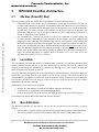
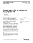
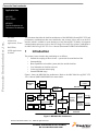
Freescale Semiconductor
Application Note
AN2335/D
Rev. 0, 10/2002
Freescale Semiconductor, Inc...
MPC8260
Dual-Bus Architecture and
Performance Considerations
Eric Bost,
NCSG Field
Applications, France
Paul Wilson,
NCSD Applications,
Scotland
This document describes the dual-bus architecture of the MPC8260 PowerQUICC II™ and
performance considerations that users should take into account. It does not cover the PCI
interface which is available in some derivatives of the PowerQUICC II family of integrated
communications processors (refer to the PCI Bridge Functional Specification: Addendum to
the MPC8260 PowerQUICC II™ User’s Manual (Document ID: MPC8265AUMAD/D)).
1
Introduction
The primary issues related to bus partitioning are as follows:
•
•
•
•
•
•
Internal de-coupling of the two buses—system (60x) bus and the local bus
Interoperability
Burst capabilities on both the system (60x) bus and the local bus
Core limitations on local bus accesses
Cache requirements and snooping
Internal DPRAM usage
Figure 1 shows the MPC8260 bus architecture. Refer to the MPC8260 PowerQUICC II™
User’s Manual (MPC8260UMAD/D) for more details.
External
master
I-cache
MPC603e
core
d-cache
60x bus
60x bus
arbiter
CP
ROM
Dual-Port
RAM
SDMA
60x-to-local
bridge
peripheral bus
FCC
MCC
SCC
Address
decode
registers
Memory
controller
60x bus
Memory
controller
local bus
CPM
Local bus
arbiter
Local bus
Figure 1. MPC8260 Bus Architecture
© Freescale Semiconductor, Inc., 2004. All rights reserved.
For More Information On This Product,
Go to: www.freescale.com
controller
controller
Freescale Semiconductor, Inc.
MPC8260 Dual-Bus Architecture
2
MPC8260 Dual-Bus Architecture
2.1
60x Bus (PowerPC Bus)
This is the primary system bus (64-bit data/ 32-bit address). It has two operating modes:
•
Freescale Semiconductor, Inc...
•
2.2
Single MPC8260—In this mode, slave I/O and memory devices can be connected to the 60x bus;
no other external masters are supported. All the address, data, and control lines are provided by the
internal memory controller and the dedicated signals for bus arbitration are not used. In this mode,
the MPC603e core ensures internal cache coherency for all accesses that use the 60x bus. This
means that CPM accesses can be snooped (controlled by GBL configuration bit discussed in
Section 4, “MPC8260 Cache Capability”).
60x-compatible bus—In this mode, the 60x bus allows the connection of external masters e.g.
L2 cache controller, additional processors and ASICs. It also supports externally controlled bus
snooping for cache coherency. The arbitration logic between several masters can be internal (the
MPC8260 can arbitrate up to three external masters) or can be external (for example, the MPC107).
In this mode, the MPC603e core can be disabled (meaning the MPC8260 is in slave mode). In this
mode, the MPC8260 supports one-level address pipelining by asserting AACK to the current bus
master when its data tenure starts and by granting the address bus to the next requesting device
before the current data tenure is complete. Refer to Sections 4.3.2.1, 8.4.2, and 10.9 in the
MPC8260 PowerQUICC II™ User’s Manual.
Local Bus
This is an optional 32-bit data bus which is synchronous to the system bus. It is used in conjunction with the
memory controller because only the 18 low-order address bits are provided. The local bus enhances the
operation of the high-speed communication controllers by allowing users to store connection tables and
buffer descriptors away from the system bus.
Accessing data buffers through the 60x or local bus should be considered carefully. Only buffers that do not
require heavy processing from the core should be accessed from local bus. The main reason for this
recommendation is that data accessed from the local bus cannot be cached when accessed by the MPC603e
core. Because the MPC603e core accesses to the local bus are visible on the 60x bus, the available
bandwidth on the 60x bus is reduced.
Additional uses of the local bus are as follows:
•
•
•
Interface to CAM memory (for connections address translation and look-up)
Local memory or peripheral devices handled through IDMA
Reduces the electrical load on the 60x bus, thus reducing the need for extra buffering devices
Users should note that the MPC8260 cannot boot from the local bus.
2.3
Bus Arbitration
The MPC8260 integrates two bus arbiters—one for the 60x bus and one for the local bus—as shown
Figure 1.
•
2
60x-bus arbiter—Arbitrates between the internal bus masters and up to three external bus masters.
The 60x-bus internal bus master can be either the MPC603e core and CPM (DMA block).
MPC8260 Dual-Bus Architecture and Performance Considerations
For More Information On This Product,
Go to: www.freescale.com
Freescale Semiconductor, Inc.
MPC8260 Dual-Bus Architecture
•
Local bus arbiter—Arbitrates between the CPM (DMA block) and the 60x-to-local bus bridge. The
local bus masters can be the CPM, the MPC603e core, or the external bus masters on the 60x bus.
Freescale Semiconductor, Inc...
Arbitration priorities and bus parking are configurable. Refer to Section 4.3.2 in the MPC8260
PowerQUICC II™ User’s Manual.
2.4
Bus Access
2.4.1
CPU Bus Access
As shown in Figure 1, the MPC603e core has direct access to the 60x bus. Therefore, all bus transactions
from the MPC603e core must arbitrate and use the 60x bus, even if the transaction is directed to the local
bus (through the 60x-to-local bridge controlled by the memory controller). This is also the case when the
MPC603e core makes an access to internal dual-port RAM. Obviously, MPC603e-core accesses to the
internal caches do not require a 60x bus transaction on cache hits.
2.4.2
CPM Bus Access
When considering CPM resources, two kinds of transactions must be distinguished:
•
•
Internal-CPM transactions to the microcode resources (code and data)
DMA-initiated transactions for the transfer of data units between the serial controllers—for
example, an FCC running ATM with transmit / receive buffers in external memory
For internal-transactions, the CPM has its own internal path and does not imply systematic usage of either
the local or 60x buses. For example, data exchanges between communication ports and internal dual-port
RAM use the CPM peripheral bus and do not use the local or 60x bus.
When the CPM needs to access external memory (accesses to buffer descriptors and buffers under control
of SDMA block), it issues an arbitration request to either the local bus or the 60x bus, depending on a
configuration parameter selectable for each single data structure, as shown in the following examples:
•
•
•
An FCC operating in ATM mode—It is possible to direct the CPM to access data buffers on either
the 60x or local bus for each virtual connection. Refer to Section 29.10.2 in the MPC8260
PowerQUICC II™ User’s Manual.
An FCC operating in Ethernet mode—The bus selection is more global as described in Section
28.7.1 of the MPC8260 PowerQUICC II™ User’s Manual.
For IDMA, the CPM can perform fast data transfers between memory or peripheral devices located
on either the system (60x) or local bus.
It is recommended that users locate buffer descriptors and buffers in external memory. However, buffer
descriptors and buffers can be located in internal DPRAM. In this case, DMA-initiated transactions are at
first issued on the system (60x) because DPRAM internally is considered a slave on the system (60x) bus.
2.5
Performance Issues
Because of its 64-bit data port size and the 32-byte burst capability, the system (60x) bus provides more
bandwidth than the local bus. The 60x bus also supports one-level address pipelining, which can improve
data throughput by allowing the memory controlled hardware to decode a set of address and control signals
while the current data transaction finishes. Pipelining works in single-MPC8260 mode and 60x-bus
MPC8260 Dual-Bus Architecture and Performance Considerations
For More Information On This Product,
Go to: www.freescale.com
3
Freescale Semiconductor, Inc.
MPC8260 Memory Controller
compatible mode. The CPM serial DMA controller is one of the bus masters on the 60x bus and can take
advantage of the pipeline like other bus masters.
The MPC603e core itself cannot burst to the local bus. However, the CPM can do DMA bursts to memory
devices on the local bus. A performance penalty ratio from 2 to 10 can affect application software when data
is accessed from the core using the local bus.
Freescale Semiconductor, Inc...
Thus, simultaneous activity on both buses is possible when the CPM uses the local bus to access connection
tables while the MPC603e core uses the 60x bus to access data buffers. Concurrent accesses on both buses
are also allowed from the CPM in the case of IDMA single address (s) transfers. For dual-address transfers,
the accesses are not concurrent. The CPM will do a read first, followed by a write.
The minimum delay between consecutive transactions on the local bus is five cycles. These cycles are
comprised from the pipelining of bus arbitration and control signals between the 60x/local bus (TS and TA).
This minimum delay can be achieved if the 60x bus pipelining feature is fully utilized, i.e. if all new
loads/stores begin their address phase while the current load/store finishes its data phase.
Using internal DPRAM to locate CPM data structures—for example, buffer descriptors and buffers in the
DPRAM—does not provide the best bus performance. Also, internal DPRAM cannot be cached by the core.
3
MPC8260 Memory Controller
The MPC8260 memory controller allows control of various types of memory and slave I/O devices.
Because of the dual-bus architecture of the MPC8260, the memory controller provides two sets of state
machines for both the local and the 60x buses. For a given memory partition, the allocation to a given state
machine working on a given bus is determined by configuring the Base register (BRx) MS bit. Refer to
Section 10.2 in the MPC8260 PowerQUICC II™ User’s Manual.
When a transaction is initiated by the MPC603e core and the 60x bus is granted by the 60x bus arbiter, the
address is compared for a match in one of BRx. If a match occurs, BRx[MS] selects a state machine
(SDRAM, UPM or GPCM) and a bus (local or 60x). If the 60x bus is selected, access continues (if it has
already been arbitrated) and the memory controller signals are generated to control the memory or
peripheral device. If the local bus is selected, the local bus arbiter gives priority to this transaction. Note that
in this case, the local bus transactions are visible on the 60x bus.
When a transaction is requested by the CPM (SDMA), it is arbitrated either by the local bus arbiter or the
60x bus arbiter (depending on each data structure configuration). Then, the address is compared with BRx
to select a given state machine and a bus.
In the special case when a transaction is requested by the CPM, is arbitrated by the local bus arbiter, and the
BRx selects the 60x bus, the transaction is ignored. This case must be prevented in software because there
is no local-to-60x bridge.
Alternatively, when a transaction is requested by the CPM, is arbitrated by the 60x bus arbiter, and BRx
selects the local bus, the transaction is processed through the 60x-to-local bridge. Again, software should
prevent this case from occurring.
Regardless of whether the MPC603e core is disabled or enabled, the memory controller and DPRAM on
MPC8260 can be accessed by external masters. As a consequence, external masters can access the
MPC8260 local bus through the 60x-to-local bridge. Refer to Section 10.9 in the MPC8260 PowerQUICC
II™ User’s Manual.
4
MPC8260 Dual-Bus Architecture and Performance Considerations
For More Information On This Product,
Go to: www.freescale.com
Freescale Semiconductor, Inc.
MPC8260 Cache Capability
In single MPC8260 mode, the 60x bus is controlled by the memory controller, and in this mode 60x bus
signals (TS, TSIZ[0–3], TT[0–4] etc.) have no timing relationship to the address bus or chip select signals
(CS[0–11]).
4
MPC8260 Cache Capability
To clarify the MPC8260’s cache capability, the following situations need to be differentiated:
Freescale Semiconductor, Inc...
•
•
•
5
Internal caches on the MPC603e core require a burst access to refill a cache line (cache line is 32
bytes). The MPC603e core cannot burst on the local bus and thus, all memory partitions placed on
the local bus must be set as non-cacheable using the PowerPC architecture-compliant memory
management units (MMUs). Execution from the core through the local bus to non-cacheable
memory may be possible: program fetches are 64-bit loads, but only single accesses are performed
in that case. For performance reasons, this scenario is not recommended and only data should be
accessed from local bus.
Accesses initiated by the CPM through the 60x bus to cacheable partitions are allowed and
coherency is enforced by internal snooping. To enforce snooping for those memory partitions, the
global (GBL) bit has to be set in the appropriate CPM registers and parameters—for example, in
the case of an FCC operating in ATM mode. Refer to Sections 28.7.1, 29.10.2.2, and 29.19.2.3 in
the MPC8260 PowerQUICC II™ User’s Manual. Note that there is no snooping if the GBL bit is
not set.
Accesses initiated by the CPM through the local bus. As the 60x bus does not see the transaction,
there is no snooping and software should ensure that the snooping bit is turned off.
MPC8260 Burst Capability and Restrictions
To understand the MPC8260’s burst capability, its should be noted that a burst could occur in two situations:
•
•
Burst initiated from the source of the transaction (MPC603e core or CPM)
Burst initiated effectively by the MPC8260 memory controller depending on its mode of operation
The MPC603e core initiates burst transactions to the 60x bus each time a cache line is filled or cast out. A
burst initiated from the memory controller depends on its mode of operation and the memory device
capability (SDRAM- or UPM-controlled DRAM support burst). In the case of a GPCM- or UPM-controlled
non-burstable device, the memory controller splits the burst request transaction into several successive
single beat transactions.
The CPM SDMA controllers are capable of bursting on both the 60x bus and the local bus.
60x bus masters cannot burst to DPRAM, registers, nor the local bus. A burst to these destinations is
terminated with TEA. Memory partitions that may be accessed from the core through the local bus, must be
non-cacheable.The memory controller with the 60x-to-local bridge is not able to split the burst requested
transaction into several successive single beat transactions.
Consequently, the 60x core-to-local-bus path provides lower performance. This is a limitation of the
architecture and users should not use the local bus to store data structures to which the MPC603e core
requires high-bandwidth access. IDMA should be used to transfer large blocks of data between the 60x and
local buses as it is capable of bursting on both buses.
MPC8260 Dual-Bus Architecture and Performance Considerations
For More Information On This Product,
Go to: www.freescale.com
5
Freescale Semiconductor, Inc.
Snooping and Performance Considerations
6
Snooping and Performance Considerations
The MPC8260 provides dedicated hardware to ensure memory coherency by snooping bus transactions, by
maintaining information about the status of data in a cache block, and by the address retry capability. Refer
to Section 8.6 and Section 8.4.4.1 in the MPC8260 PowerQUICC II™ User’s Manual.
Asserting the global (GBL) output signal indicates whether the current transaction must be snooped by other
snooping devices on the bus. Accesses which use this feature cause the MPC8260 memory controller to wait
a certain number of cycles—determined by BCR[APD] for ARTRY assertion—before initiating the
memory access. Refer to Section 4.26 in the MPC8260 PowerQUICC II™ User’s Manual.
Freescale Semiconductor, Inc...
Care must be taken to minimize the use of this global feature because using the ARTRY signal to enforce
coherency can require significant bus bandwidth.
Accesses initiated by the CPM through the 60x bus to cached memory areas can be snooped without using
the ARTRY signal. This can be accomplished by setting the global (GBL) bit in the appropriate CPM
registers and parameters to enable snooping. Refer to Sections 28.7.1, 29.10.2.2, and 29.19.2.3 in the
MPC8260 PowerQUICC II™ User’s Manual. For example, if a cached memory area is marked write
through and the CPM transfers data to this memory area then bus snooping marks this cached area as invalid.
However, if a cached memory area is marked write back or cache tags are being updated when the CPM
transfers data, then ARTRY is used.
Users should consider the above factors in the following scenarios:
•
•
•
•
In Single-MPC8260 mode, the CPU should define all its memory space as non-global (even if it is
shared with the CPM). This can be done since the CPM has no L1 cache. The CPM should define
the shared memory areas as global. So, when the CPM makes an access to a shared memory, the
core is notified about it, but when the core access the same area, there is no need to use the global
signal.
The above applies for a MPC8260 with L2 cache system, since L2 can never cache DMA accesses
and it retries the bus only if the DMA tries to access an area previously accessed by the core.
If the internal CPU is disabled and an external core is used, the two previous scenarios still apply.
The only time the CPU should define a memory area as shared is when it is shared with another
CPU (and not the CPM).
In summary, users should try to avoid shared memory as much as possible. In cases where this is required,
only the CPM should use the snooping option and the CPU should not.
The CPU should define a memory space as shared (global) only if it is actually shared with another CPU
(and not the CPM). This can happen only in multi-processor systems.
6
MPC8260 Dual-Bus Architecture and Performance Considerations
For More Information On This Product,
Go to: www.freescale.com
Freescale Semiconductor, Inc.
Freescale Semiconductor, Inc...
Snooping and Performance Considerations
MPC8260 Dual-Bus Architecture and Performance Considerations
For More Information On This Product,
Go to: www.freescale.com
7
Freescale Semiconductor, Inc.
How to Reach Us:
Home Page:
www.freescale.com
E-mail:
[email protected]
Freescale Semiconductor, Inc...
USA/Europe or Locations Not Listed:
Freescale Semiconductor
Technical Information Center, CH370
1300 N. Alma School Road
Chandler, Arizona 85224
+1-800-521-6274 or +1-480-768-2130
[email protected]
Europe, Middle East, and Africa:
Freescale Halbleiter Deutschland GmbH
Technical Information Center
Schatzbogen 7
81829 Muenchen, Germany
+44 1296 380 456 (English)
+46 8 52200080 (English)
+49 89 92103 559 (German)
+33 1 69 35 48 48 (French)
[email protected]
Japan:
Freescale Semiconductor Japan Ltd.
Headquarters
ARCO Tower 15F
1-8-1, Shimo-Meguro, Meguro-ku,
Tokyo 153-0064
Japan
0120 191014 or +81 3 5437 9125
[email protected]
Asia/Pacific:
Freescale Semiconductor Hong Kong Ltd.
Technical Information Center
2 Dai King Street
Tai Po Industrial Estate
Tai Po, N.T., Hong Kong
+800 2666 8080
[email protected]
For Literature Requests Only:
Freescale Semiconductor Literature Distribution Center
P.O. Box 5405
Denver, Colorado 80217
1-800-441-2447 or 303-675-2140
Fax: 303-675-2150
[email protected]
Information in this document is provided solely to enable system and software
implementers to use Freescale Semiconductor products. There are no express or
implied copyright licenses granted hereunder to design or fabricate any integrated
circuits or integrated circuits based on the information in this document.
Freescale Semiconductor reserves the right to make changes without further notice to
any products herein. Freescale Semiconductor makes no warranty, representation or
guarantee regarding the suitability of its products for any particular purpose, nor does
Freescale Semiconductor assume any liability arising out of the application or use of
any product or circuit, and specifically disclaims any and all liability, including without
limitation consequential or incidental damages. “Typical” parameters which may be
provided in Freescale Semiconductor data sheets and/or specifications can and do
vary in different applications and actual performance may vary over time. All operating
parameters, including “Typicals” must be validated for each customer application by
customer’s technical experts. Freescale Semiconductor does not convey any license
under its patent rights nor the rights of others. Freescale Semiconductor products are
not designed, intended, or authorized for use as components in systems intended for
surgical implant into the body, or other applications intended to support or sustain life,
or for any other application in which the failure of the Freescale Semiconductor product
could create a situation where personal injury or death may occur. Should Buyer
purchase or use Freescale Semiconductor products for any such unintended or
unauthorized application, Buyer shall indemnify and hold Freescale Semiconductor
and its officers, employees, subsidiaries, affiliates, and distributors harmless against all
claims, costs, damages, and expenses, and reasonable attorney fees arising out of,
directly or indirectly, any claim of personal injury or death associated with such
unintended or unauthorized use, even if such claim alleges that Freescale
Semiconductor was negligent regarding the design or manufacture of the part.
AN2335/D
For More Information On This Product,
Go to: www.freescale.com