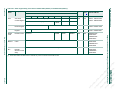
1
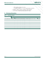
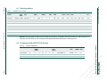
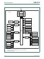
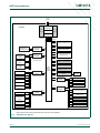
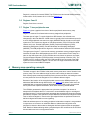
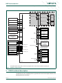
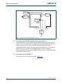
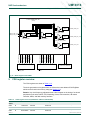
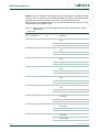
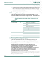
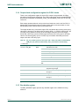
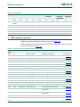
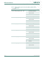
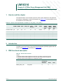
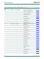
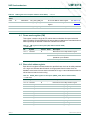
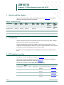
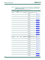
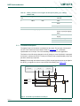
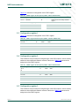
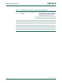
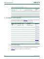
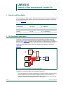
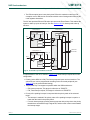
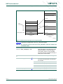
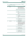
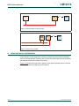
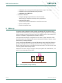
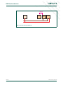
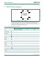
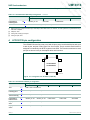
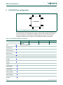
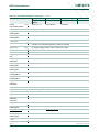
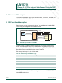
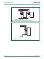
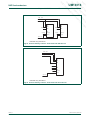
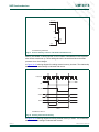
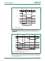
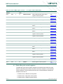
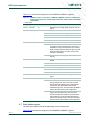
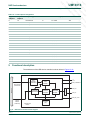
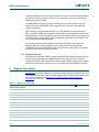
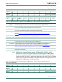
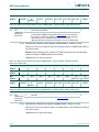
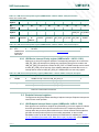
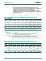
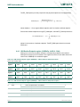
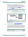
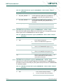
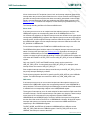
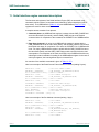
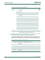
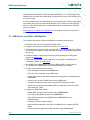
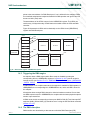
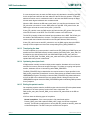
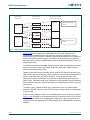
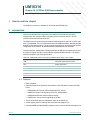
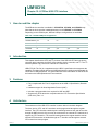
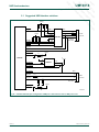
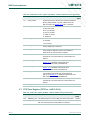
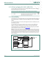
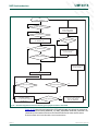
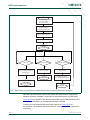
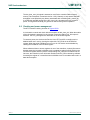
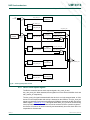
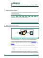
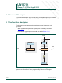
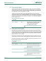
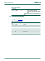
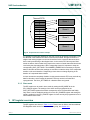
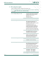
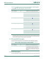
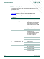
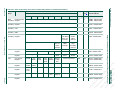
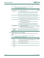
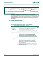
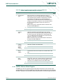
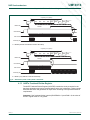
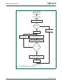
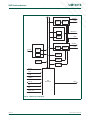
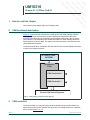
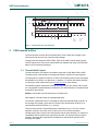
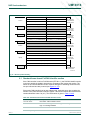
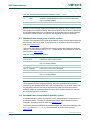
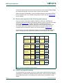
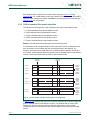
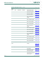
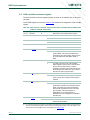
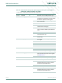
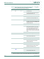
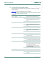
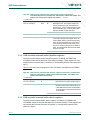
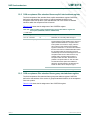
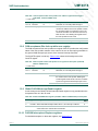
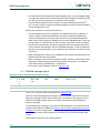
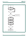
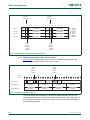
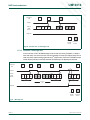
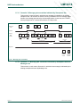
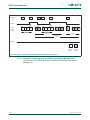
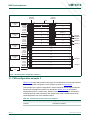
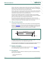
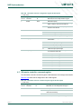
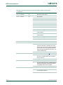
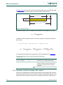
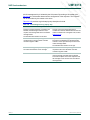
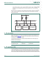
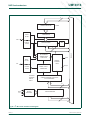
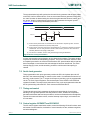
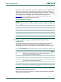
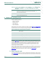
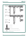
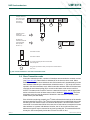
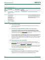
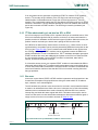
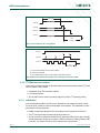
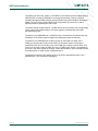
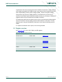
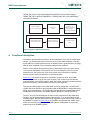
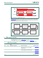
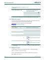
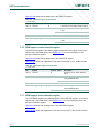
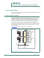
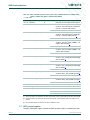
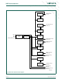
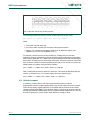
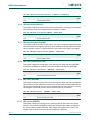
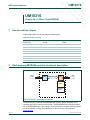
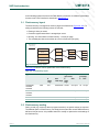
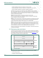
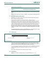
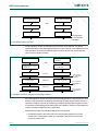
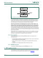
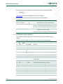
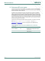
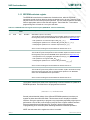
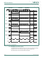
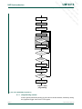
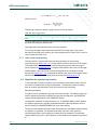
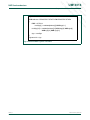
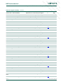
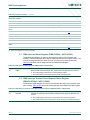
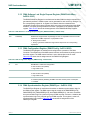
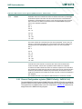
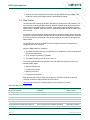
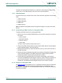
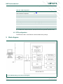
D
D
R
R
R
R
R
D
D
D
A
A
A
A
A
FT
FT
D
R
R
FT
FT
FT
FT
A
A
A
A
R
R
D
D
D
Chapter 28: LPC29xx Flash/EEPROM
D
R
R
A
FT
FT
FT
A
A
R
R
D
D
D
D
Corresponding sector is Read-Only
FT
FT
A
A
R
R
D
Corresponding sector is Read/Write (default)
All bits ‘0’
F
FT
FT
All bits ‘1’
A
A
A
Description
R
R
R
Flash-word value
D
D
D
Table 413. Sector security values
FT
UM10316
FT
FT
NXP Semiconductors
D
D
R
A
FT
D
R
Remark: After enabling flash memory security, this feature is not activated until the next
reset.
A
Remark: When flash memory security is enabled, it is not possible to disable this feature.
2.7 EEPROM functional description
EEPROM is a non-volatile memory mostly used for storing relatively small amounts of
data, for example for storing settings.
There are three operations for accessing the memory: reading, writing and
erase/program. “Writing” to memory is split up into two separate operations, writing and
erase/program. The first operation which will be called “writing” in this document is not
really updating the memory, but only updating the temporary data register called the “page
register”. The page register needs to be written with minimum 1 byte and maximum 8
bytes before the second operation which is called “erase/program” in this document can
be used to actually update the non-volatile memory. Note that the data written to the page
register is not “cached”, it can’t be read before it is actually programmed into non-volatile
memory.
The 64-byte page register, present in every EEPROM device, is exactly the size of a page
in memory. One device contains 256 pages and is in total 16 kB big.
2.8 Addressing
[13:6]
[5:0]
8 MSB bits (selects a page)
6 LSB bits (selects a byte in the
page register)
Fig 122. Address fields
When doing a write operation the LSB bits need to be used to select a byte in a page
register. For a write operation the MSB bits are don’t care. It is possible to write to different
page register before starting an erase/program operation on any device.
For an erase/program operation the LSB bits are don’t care. The MSB bits are needed to
select the page. During the erase/program operation the other devices can still be
accessed.
When doing a read operation all the address fields are needed.
2.9 Initialization
Remark: The minimum operating voltage for the data EEPROM is Vdd = 1.5 V.
UM10316_0
User manual
© NXP B.V. 2008. All rights reserved.
Rev. 00.06 — 17 December 2008
482 of 571