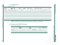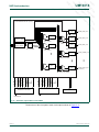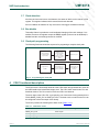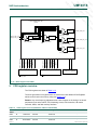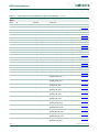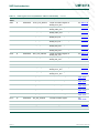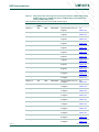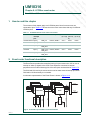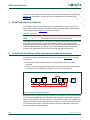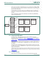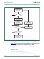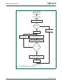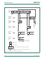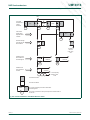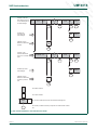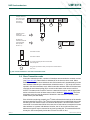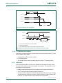
1
R
R
R
R
R
A
A
A
A
A
FT
FT
FT
FT
FT
D
R
R
A
A
FT
FT
FT
FT
A
A
R
R
D
D
D
D
R
R
A
FT
FT
FT
A
A
R
R
D
D
D
LPC29xx ARM9 microcontroller with CAN and LIN
R
A
F
FT
FT
A
A
R
R
D
D
User manual
D
Rev. 00.06 — 17 December 2008
D
D
D
D
D
UM10316
D
FT
FT
A
A
R
R
D
D
D
R
A
FT
D
R
A
Document information
Info
Content
Keywords
LPC2917/01; LPC2919/01; LPC2927; LPC2929; LPC2921; LPC2923;
LPC2925; LPC2930; LPC2939 User Manual, ARM9, CAN, LIN
Abstract
This document extends the LPC29xx data sheets with additional details to
support both hardware and software development. It focuses on functional
description and typical application use.
FT
FT
D
R
R
D
A
FT
R
F
D
FT
FT
A
A
R
R
D
D
D
R
List of external pins to event router updated.
CFID chapter added.
Flash/EEPROM chapter updated.
Parts LPC2921/23/25, LPC2930, and LPC2939 added.
CGU0 PLL input clock frequency restricted to <= 25 MHz.
UART modem control and RS485 control registers added.
I2C pin description and pin usage updated.
Numerous editorial updates throughout the manual.
USB host chapter added.
GPDMA connections updated. GPDMA is not connected to the I2C.
Memory-to-memory transactions are enabled for timers, GPIOs, and WDT.
PMU chapter, BASE_STAT register updated.
USB OTG chapter: dual USB port added (LPC2930/39).
Initial version
For more information, please visit: http://www.nxp.com
For sales office addresses, please send an email to: [email protected]
UM10316_0
© NXP B.V. 2008. All rights reserved.
Rev. 00.06 — 17 December 2008
2 of 571
A
•
•
•
PMU chapter updated.
R
RGU chapter updated.
SCU chapter: description of SFSP_5_18/18, SEC_DIS, and SEC_STA registers
added.
D
•
•
•
•
•
•
•
•
•
•
•
FT
CGU chapter updated with description of CGU1 and internal base clocks.
A
•
•
Contact information
User manual
A
FT
FT
A
A
R
R
D
D
D
<tbd>
R
R
FT
FT
A
A
R
R
D
D
D
Modifications:
00.05
FT
FT
FT
<tbd>
A
A
LPC29xx
FT
A
A
R
R
D
D
D
00.06
Description
FT
UM10316
FT
FT
Date
A
A
A
A
A
Rev
R
R
R
R
R
Revision history
D
D
D
D
D
NXP Semiconductors
A
A
A
A
A
FT
FT
FT
FT
FT
D
R
R
A
A
FT
FT
FT
FT
A
A
R
R
D
D
D
D
R
R
A
FT
FT
FT
A
A
R
R
D
D
D
R
A
F
FT
FT
A
A
R
R
D
D
User manual
D
Rev. 00.06 — 17 December 2008
R
R
R
R
R
Chapter 1: LPC29xx Introductory information
D
D
D
D
D
UM10316
D
FT
FT
A
A
R
R
D
D
D
1. Introduction
R
A
Remark: See Table 1–2 for feature details for each LPC29xx part.
• ARM968E-S processor running at frequencies of up to 125 MHz maximum.
• Multi-layer AHB system bus at 125 MHz with four separate layers.
• On-chip memory:
– Two Tightly Coupled Memories (TCM), up to 32 kB Instruction (ITCM), up to 32 kB
Data TCM (DTCM).
– Two separate internal Static RAM (SRAM) instances; 32 kB SRAM and 16 kB
SRAM.
– 8 kB ETB SRAM.
– Up to 768 kB flash-program memory with 16 kB EEPROM.
• Dual-master, eight-channel GPDMA controller on the AHB multilayer matrix which can
be used with the SPI interfaces and the UARTs, as well as for memory-to-memory
transfers including the TCM memories.
• External Static Memory Controller (SMC) with eight memory banks; up to 32-bit data
bus; up to 24-bit address bus.
• Serial interfaces:
– USB 2.0 full-speed device/OTG controller with dedicated DMA controller and
on-chip PHY for device and Host (LPC2930/39 only) functions.
– Two-channel CAN controller supporting Full-CAN and extensive message filtering
– Two LIN master controllers with full hardware support for LIN communication.
– Two 550 UARTs with 16-byte Tx and Rx FIFO depths, DMA support, and RS485
support.
UM10316_0
User manual
© NXP B.V. 2008. All rights reserved.
Rev. 00.06 — 17 December 2008
3 of 571
A
3. General features
R
This document describes the following parts: LPC2917/01, LPC2919/01, LPC2921,
LPC2923, LPC2925, LPC2927, LPC2929, LPC2930, and LPC2939. Differences between
the various parts as they apply to each block or peripheral are listed at the beginning of
each chapter. For an overview of features see Table 1–2.
D
2. About this user manual
FT
The LPC29xx combine an 125 MHz ARM968E-S CPU core, Full Speed USB 2.0 OTG
and device, CAN and LIN, 56 kB SRAM, up to 768 kB flash memory, external memory
interface, three 10-bit ADCs, and multiple serial and parallel interfaces in a single chip
targeted at consumer, industrial, medical, and communication. To optimize system power
consumption, the LPC29xx has a very flexible Clock Generation Unit (CGU) that provides
dynamic clock gating and scaling.
D
D
R
R
R
R
R
D
D
D
D
R
R
D
R
R
A
FT
FT
FT
A
A
R
R
D
D
D
R
A
F
FT
FT
A
A
R
R
D
D
D
D
FT
FT
A
A
R
R
D
D
D
• Other peripherals:
R
A
– Two dedicated 32-bit timers to schedule and synchronize PWM and ADC.
– Quadrature encoder interface that can monitor one external quadrature encoder.
– 32-bit watchdog with timer change protection, running on safe clock.
• Up to 108 general-purpose I/O pins with programmable pull-up, pull-down, or bus
keeper.
• Vectored Interrupt Controller (VIC) with 16 priority levels.
• Up to 24 level-sensitive external interrupt pins, including CAN and LIN wake-up
features.
Configurable clock-out pin for driving external system clocks.
Processor wake-up from power-down via external interrupt pins; CAN or LIN activity.
Flexible Reset Generator Unit (RGU) able to control resets of individual modules.
Flexible Clock-Generation Unit (CGU) able to control clock frequency of individual
modules:
– On-chip very low-power ring oscillator; fixed frequency of 0.4 MHz; always on to
provide a Safe_Clock source for system monitoring.
– On-chip crystal oscillator with a recommended operating range from 10 MHz to
25 MHz - max. PLL input 25 MHz.
– On-chip PLL allows CPU operation up to a maximum CPU rate of 125 MHz.
– Generation of up to 11 base clocks.
– Seven fractional dividers.
• Highly configurable system Power Management Unit (PMU):
clock control of individual modules.
allows minimization of system operating power consumption in any configuration.
• Standard ARM test and debug interface with real-time in-circuit emulator.
• Boundary-scan test supported.
• ETM/ETB debug functions with 8 kB of dedicated SRAM also accessible for
application code and data storage.
• Dual power supply:
© NXP B.V. 2008. All rights reserved.
4 of 571
A
– Four six-channel PWMs (Pulse-Width Modulators) with capture and trap
functionality.
R
– Four 32-bit timers each containing four capture-and-compare registers linked to
I/Os.
D
– Multiple trigger-start option for all ADCs: timer, PWM, other ADC and external
signal input.
FT
– Up to three ADCs: Two 10-bit ADCs, 8-channels each, with 3.3 V measurement
range and one, 8-channel 10-bit ADC with 5.0 V measurement range provide a
total of up to 24 analog inputs, with conversion times as low as 2.44 μs per
channel. Each channel provides a compare function to minimize interrupts.
Rev. 00.06 — 17 December 2008
FT
FT
FT
FT
– Two I2C-bus interfaces.
User manual
A
A
A
A
R
R
D
D
D
– Three full-duplex Q-SPIs with four slave-select lines; 16 bits wide; 8 locations
deep; Tx FIFO and Rx FIFO.
UM10316_0
FT
FT
FT
FT
FT
UM10316
Chapter 1: LPC29xx Introductory information
•
•
•
•
A
A
A
A
A
NXP Semiconductors
D
D
R
R
R
R
R
D
D
D
A
A
A
A
A
FT
FT
D
R
R
D
R
R
A
FT
FT
FT
A
A
R
R
D
D
D
R
A
F
FT
FT
A
A
R
R
D
D
D
D
FT
FT
A
A
R
R
D
• Available in 100-pin,144-pin, and 208-pin LQFP packages.
• −40 °C to 85 °C ambient operating temperature range.
FT
FT
FT
FT
– I/O operating voltage: 2.7 V to 3.6 V; inputs tolerant up to 5.5 V.
A
A
A
A
R
R
D
D
D
Chapter 1: LPC29xx Introductory information
– CPU operating voltage: 1.8 V ± 5 %.
FT
UM10316
FT
FT
NXP Semiconductors
D
D
R
A
FT
R
A
Table 1.
D
4. Ordering information
Ordering information
Type number
Package
Name
Description
Version
LQFP144 plastic low profile quad flat package; 144 leads; body 20 × 20 × 1.4 mm
SOT486-1
LPC2919FBD144/01
LQFP144 plastic low profile quad flat package; 144 leads; body 20 × 20 × 1.4 mm
SOT486-1
LPC2921FBD100
LQFP100 plastic low profile quad flat package; 100 leads; body 14 x 14 x 1.4 mm
SOT407-1
LPC2923FBD100
LQFP100 plastic low profile quad flat package; 100 leads; body 14 x 14 x 1.4 mm
SOT407-1
LPC2925FBD100
LQFP100 plastic low profile quad flat package; 100 leads; body 14 x 14 x 1.4 mm
SOT407-1
LPC2927FBD144
LQFP144 plastic low profile quad flat package; 144 leads; body 20 × 20 × 1.4 mm
SOT486-1
LPC2929FBD144
LQFP144 plastic low profile quad flat package; 144 leads; body 20 × 20 × 1.4 mm
SOT486-1
LPC2930FBD208
LQFP208 plastic low profile quad flat package; 208 leads; body 28 x 28 x 1.4 mm
SOT459-1
LPC2939FBD208
LQFP208 plastic low profile quad flat package; 208 leads; body 28 x 28 x 1.4 mm
SOT459-1
LPC2917FBD144/01
UM10316_0
User manual
© NXP B.V. 2008. All rights reserved.
Rev. 00.06 — 17 December 2008
5 of 571
xxxxxxxxxxxxxxxxxxxxx xxxxxxxxxxxxxxxxxxxxxxxxxx xxxxxxx x x x xxxxxxxxxxxxxxxxxxxxxxxxxxxxxx xxxxxxxxxxxxxxxxxxx xx xx xxxxx
xxxxxxxxxxxxxxxxxxxxxxxxxxx xxxxxxxxxxxxxxxxxxx xxxxxx xxxxxxxxxxxxxxxxxxxxxxxxxxxxxxxxxxx xxxxxxxxxxxx x x
xxxxxxxxxxxxxxxxxxxxx xxxxxxxxxxxxxxxxxxxxxxxxxxxxxx xxxxx xxxxxxxxxxxxxxxxxxxxxxxxxxxxxxxxxxxxxxxxxxxxxxxxxx xxxxxxxx
xxxxxxxxxxxxxxxxxxxxxxxxx xxxxxxxxxxxxxxxxxxxx xxx
Table 2.
NXP Semiconductors
UM10316_0
User manual
4.1 Ordering options
LPC29xx part overview
Part
number
Flash
SRAM TCM
(incl
(I/D)
ETB)
LPC2939
768 kB
56 kB
LPC2930
-
LPC2929
CAN
Rev. 00.06 — 17 December 2008
LIN/
Pins
UART
UART SPI
RS485
3V3
ADC
5 V SMC
ADC
USB
device
USB
host
USB ETM
OTG
QEI
I2C-bus
Clkout
pin
32/32 kB 2
2
208
2
3
2
Yes
Yes
Yes
Yes
Yes
Yes
Yes
Yes
Yes
56 kB
32/32 kB 2
2
208
2
3
2
Yes
Yes
Yes
Yes
Yes
Yes
Yes
Yes
Yes
768 kB
56 kB
32/32 kB 2
2
144
2
3
2
Yes
Yes
Yes
No
Yes
Yes
Yes
Yes
Yes
LPC2927
512 kB
56 kB
32/32 kB 2
2
144
2
3
2
Yes
Yes
Yes
No
Yes
Yes
Yes
Yes
Yes
LPC2925
512 kB
40 kB
16/16 kB 2
2
100
2
3
2
No
No
Yes
No
No
Yes
Yes
Yes
Yes
LPC2923
256 kB
24 kB
16/16 kB 2
2
100
2
3
2
No
No
Yes
No
No
Yes
Yes
Yes
Yes
LPC2921
128 kB
24 kB
16/16 kB 2
2
100
2
3
2
No
No
Yes
No
No
Yes
Yes
Yes
Yes
LPC2919/01 768 kB
56 kB
16/16 kB 2
2
144
2
3
2
No
Yes
No
No
No
Yes
Yes
Yes
Yes
LPC2917/01 512 kB
56 kB
16/16 kB 2
2
144
2
3
2
No
Yes
No
No
No
Yes
Yes
Yes
Yes
Remark: Note that parts LPC2927 and LPC2929 are not fully pin compatible with parts LPC2917/01 and LPC2919/01 or
LPC2917 and LPC2919. On the LPC2927/29 the MSCSS and timer blocks have a reduced pinout.
4.2 Comparison with LPC2917/19 devices
Feature comparison
Parts
GPDMA UART I2C
RS485
mode
QEI
CAN LIN USB
OTG/
device
Flash
LPC2917/19
no
EEPROM SRAM
total
ETB
SRAM
5V
ADC
no
no
no
2
2
no
512/768 kB no
80 kB
no
no
LPC2917/19/01 yes
yes
yes
yes
2
2
no
512/768 kB yes
88 kB
8 kB
no
LPC2927/29
yes
yes
yes
2
2
yes
512/768 kB yes
120 kB
8 kB
yes
yes
D
A
FT
FT
R
D
A
R
A
R
FT
D
FT
R
FT
D
UM10316
FT
R
D
FT
A
6 of 571
© NXP B.V. 2008. All rights reserved.
D
D
D
D
D
R
R
R
R
R
A
A
A
A
A
FT
FT
FT
FT
FT
D
D
D
D
R
R
R
R
A
A
A
A
F
F
F
F
T
T
T
T
Chapter 1: LPC29xx Introductory
information
D
D
D
D
R
R
R
R
A
A
A
Table 3.
D
A
R
F
D
A
A
R
FT
D
D
D
R
R
R
R
R
D
D
D
A
A
A
A
A
FT
FT
D
R
R
FT
FT
FT
FT
A
A
A
A
R
R
D
D
D
Chapter 1: LPC29xx Introductory information
D
R
R
A
FT
FT
FT
A
A
R
R
D
D
D
R
A
F
FT
FT
A
A
R
R
D
D
D
5. Block diagram
FT
UM10316
FT
FT
NXP Semiconductors
D
FT
FT
A
A
R
R
D
D
D
JTAG
interface
R
A
FT
D
R
A
TEST/DEBUG
INTERFACE
LPC2917/01
LPC2919/01
ITCM
16 kB
DTCM
16 kB
8 kB SRAM
ARM968E-S
1 × master
2 × slave
VECTORED
INTERRUPT
CONTROLLER
AHB TO DTL
BRIDGE
master
slave
master
slave
slave
CLOCK
GENERATION
UNIT CGU0/1
GPDMA CONTROLLER
AHB TO DTL
BRIDGE
GPDMA REGISTERS
slave
RESET
GENERATION
UNIT
EXTERNAL STATIC
MEMORY CONTROLLER
slave
EMBEDDED SRAM 16 kB
POWER
MANAGEMENT
UNIT
slave
EMBEDDED SRAM 32 kB
slave
slave
TIMER0/1 MTMR
AHB TO APB
BRIDGE
PWM0/1/2/3
AHB
MULTI
LAYER
MATRIX
EMBEDDED FLASH
512/768 kB
16 kB
EEPROM
slave
AHB TO APB
BRIDGE
SYSTEM CONTROL
EVENT ROUTER
3.3 V ADC1/2
CHIP FEATURE ID
slave
QUADRATURE
ENCODER
CAN0/1
AHB TO APB
BRIDGE
AHB TO APB
BRIDGE
slave
GENERAL PURPOSE I/O
PORTS 0/1/2/3
TIMER 0/1/2/3
GLOBAL
ACCEPTANCE
FILTER
SPI0/1/2
RS485 UART0/1
LIN0/1
WDT
I2C0/1
002aad959
Grey-shaded blocks represent peripherals with connections to the GPDMA.
Fig 1.
LPC2917/19/01 block diagram
UM10316_0
User manual
© NXP B.V. 2008. All rights reserved.
Rev. 00.06 — 17 December 2008
7 of 571
D
D
R
R
R
R
R
D
D
D
A
A
A
A
A
FT
FT
FT
UM10316
FT
FT
D
R
R
FT
FT
FT
FT
Chapter 1: LPC29xx Introductory information
A
A
A
A
R
R
D
D
D
NXP Semiconductors
D
R
R
A
FT
FT
FT
A
A
R
R
D
D
D
R
A
F
FT
FT
A
A
R
R
D
D
D
D
FT
FT
A
A
R
R
D
JTAG
interface
D
D
R
A
R
DTCM
16 kB
A
8 kB SRAM
D
ITCM
16 kB
FT
TEST/DEBUG
INTERFACE
LPC2921/2923/2925
ARM968E-S
1 master
2 slaves
master
master
VECTORED
INTERRUPT
CONTROLLER
CLOCK
GENERATION
UNIT
RESET
GENERATION
UNIT
AHB TO DTL
BRIDGE
slave
PWM0/1/2/3
slave
GPDMA REGISTERS
master
AHB TO DTL
BRIDGE
slave
slave
USB DEVICE
CONTROLLER
slave
power. clock, and
reset subsystem
EMBEDDED SRAM 16 kB
slave
EMBEDDED SRAM 16 kB
(LPC2925 only)
POWER
MANAGEMENT
UNIT
TIMER0/1 MTMR
GPDMA CONTROLLER
AHB TO APB
BRIDGE
slave
AHB
MULTILAYER
MATRIX
slave
EMBEDDED FLASH
512/256/128 kB
16 kB
EEPROM
slave
AHB TO APB
BRIDGE
MSC subsystem
general subsystem
SYSTEM CONTROL
EVENT ROUTER
3.3 V ADC1/2
CHIP FEATURE ID
slave
QUADRATURE
ENCODER
AHB TO APB
BRIDGE
peripheral subsystem
CAN0/1
AHB TO APB
BRIDGE
slave
GENERAL PURPOSE I/O
PORTS 0/1/5
TIMER 0/1/2/3
SPI0/1/2
GLOBAL
ACCEPTANCE
FILTER
networking subsystem
RS485 UART0/1
WDT
I2C0/1
002aae224
Grey-shaded blocks represent peripherals with connections to the GPDMA.
Fig 2.
LPC2921/23/25 block diagram
UM10316_0
User manual
© NXP B.V. 2008. All rights reserved.
Rev. 00.06 — 17 December 2008
8 of 571
D
D
R
R
R
R
R
D
D
D
A
A
A
A
A
FT
FT
FT
UM10316
FT
FT
D
R
R
FT
FT
FT
FT
Chapter 1: LPC29xx Introductory information
A
A
A
A
R
R
D
D
D
NXP Semiconductors
D
R
R
A
FT
FT
FT
A
A
R
R
D
D
D
R
A
F
FT
FT
A
A
R
R
D
D
D
D
FT
FT
A
A
R
R
D
JTAG
interface
D
D
R
A
R
DTCM
32 kB
A
8 kB SRAM
D
ITCM
32 kB
FT
TEST/DEBUG
INTERFACE
LPC2927/2929
ARM968E-S
1 master
2 slaves
master
master
VECTORED
INTERRUPT
CONTROLLER
CLOCK
GENERATION
UNIT
RESET
GENERATION
UNIT
AHB TO DTL
BRIDGE
slave
PWM0/1/2/3
slave
GPDMA REGISTERS
master
AHB TO DTL
BRIDGE
slave
slave
USB OTG/DEVICE
CONTROLLER
slave
power. clock, and
reset subsystem
slave
POWER
MANAGEMENT
UNIT
TIMER0/1 MTMR
GPDMA CONTROLLER
EXTERNAL STATIC
MEMORY CONTROLLER
EMBEDDED SRAM 16 kB
AHB TO APB
BRIDGE
slave
AHB
MULTILAYER
MATRIX
slave
EMBEDDED SRAM 32 kB
slave
EMBEDDED FLASH
512/768 kB
MSC subsystem
16 kB
EEPROM
slave
AHB TO APB
BRIDGE
3.3 V ADC1/2
general subsystem
SYSTEM CONTROL
EVENT ROUTER
5 V ADC0
CAN0/1
GLOBAL
ACCEPTANCE
FILTER
CHIP FEATURE ID
slave
QUADRATURE
ENCODER
AHB TO APB
BRIDGE
AHB TO APB
BRIDGE
slave
peripheral subsystem
networking subsystem
GENERAL PURPOSE I/O
PORTS 0/1/2/3/5
TIMER 0/1/2/3
SPI0/1/2
RS485 UART0/1
UART/LIN0/1
WDT
I2C0/1
002aae143
Grey-shaded blocks represent peripherals with connections to the GPDMA.
Fig 3.
LPC2927/29 block diagram
UM10316_0
User manual
© NXP B.V. 2008. All rights reserved.
Rev. 00.06 — 17 December 2008
9 of 571
D
D
R
R
R
R
R
D
D
D
A
A
A
A
A
FT
FT
FT
UM10316
FT
FT
D
R
R
FT
FT
FT
FT
Chapter 1: LPC29xx Introductory information
A
A
A
A
R
R
D
D
D
NXP Semiconductors
D
R
R
A
FT
FT
FT
A
A
R
R
D
D
D
R
A
F
FT
FT
A
A
R
R
D
D
D
D
FT
FT
A
A
R
R
D
JTAG
interface
D
D
R
A
R
DTCM
32 kB
A
8 kB SRAM
D
ITCM
32 kB
FT
TEST/DEBUG
INTERFACE
LPC2930
ARM968E-S
1 master
2 slaves
master
master
VECTORED
INTERRUPT
CONTROLLER
AHB TO DTL
BRIDGE
slave
GPDMA CONTROLLER
slave
GPDMA REGISTERS
master
CLOCK
GENERATION
UNIT
AHB TO DTL
BRIDGE
slave
slave
slave
power. clock, and
reset subsystem
RESET
GENERATION
UNIT
slave
POWER
MANAGEMENT
UNIT
USB HOST/OTG/DEVICE
CONTROLLER
EXTERNAL STATIC
MEMORY CONTROLLER
EMBEDDED SRAM 16 kB
AHB TO APB
BRIDGE
TIMER0/1 MTMR
slave
AHB
MULTILAYER
MATRIX
slave
EMBEDDED SRAM 32 kB
slave
AHB TO APB
BRIDGE
MSC subsystem
PWM0/1/2/3
general subsystem
3.3 V ADC1/2
AHB TO APB
BRIDGE
QUADRATURE
ENCODER
EVENT ROUTER
CHIP FEATURE ID
slave
5 V ADC0
SYSTEM CONTROL
peripheral subsystem
GENERAL PURPOSE I/O
PORTS 0/1/2/3/4/5
TIMER 0/1/2/3
AHB TO APB
BRIDGE
CAN0/1
GLOBAL
ACCEPTANCE
FILTER
slave
networking subsystem
SPI0/1/2
RS485 UART0/1
WDT
UART/LIN0/1
I2C0/1
002aae257
Grey-shaded blocks represent peripherals with connections to the GPDMA.
Fig 4.
LPC2930 block diagram
UM10316_0
User manual
© NXP B.V. 2008. All rights reserved.
Rev. 00.06 — 17 December 2008
10 of 571
D
D
R
R
R
R
R
D
D
D
A
A
A
A
A
FT
FT
FT
UM10316
FT
FT
D
R
R
FT
FT
FT
FT
Chapter 1: LPC29xx Introductory information
A
A
A
A
R
R
D
D
D
NXP Semiconductors
D
R
R
A
FT
FT
FT
A
A
R
R
D
D
D
R
A
F
FT
FT
A
A
R
R
D
D
D
D
FT
FT
A
A
R
R
D
JTAG
interface
D
D
R
A
R
DTCM
32 kB
A
8 kB SRAM
D
ITCM
32 kB
FT
TEST/DEBUG
INTERFACE
LPC2939
ARM968E-S
1 master
2 slaves
master
master
VECTORED
INTERRUPT
CONTROLLER
AHB TO DTL
BRIDGE
slave
GPDMA CONTROLLER
slave
GPDMA REGISTERS
master
CLOCK
GENERATION
UNIT
AHB TO DTL
BRIDGE
slave
slave
slave
power. clock, and
reset subsystem
RESET
GENERATION
UNIT
slave
POWER
MANAGEMENT
UNIT
USB HOST/OTG/DEVICE
CONTROLLER
EXTERNAL STATIC
MEMORY CONTROLLER
EMBEDDED SRAM 16 kB
AHB TO APB
BRIDGE
TIMER0/1 MTMR
slave
slave
EMBEDDED SRAM 32 kB
slave
EMBEDDED FLASH
768 kB
MSC subsystem
PWM0/1/2/3
AHB
MULTILAYER
MATRIX
16 kB
EEPROM
slave
AHB TO APB
BRIDGE
3.3 V ADC1/2
general subsystem
SYSTEM CONTROL
EVENT ROUTER
5 V ADC0
AHB TO APB
BRIDGE
AHB TO APB
BRIDGE
CAN0/1
GLOBAL
ACCEPTANCE
FILTER
CHIP FEATURE ID
slave
QUADRATURE
ENCODER
slave
peripheral subsystem
networking subsystem
GENERAL PURPOSE I/O
PORTS 0/1/2/3/4/5
TIMER 0/1/2/3
SPI0/1/2
RS485 UART0/1
UART/LIN0/1
WDT
I2C0/1
002aae254
Grey-shaded blocks represent peripherals with connections to the GPDMA.
Fig 5.
LPC2939 block diagram
UM10316_0
User manual
© NXP B.V. 2008. All rights reserved.
Rev. 00.06 — 17 December 2008
11 of 571
D
D
R
R
R
R
R
D
D
D
A
A
A
A
A
FT
FT
D
R
R
FT
FT
FT
FT
A
A
A
A
R
R
D
D
D
Chapter 1: LPC29xx Introductory information
D
R
R
A
FT
FT
FT
A
A
R
R
D
D
D
R
A
F
FT
FT
A
A
R
R
D
D
D
6. Functional blocks
FT
UM10316
FT
FT
NXP Semiconductors
D
FT
FT
A
A
R
R
D
This chapter gives an overview of the functional blocks, clock domains, and power modes.
See Table 1–2 for availability of peripherals and blocks for specific LPC29xx parts.
D
D
R
A
Description
Comment
Clock domain AHB
ARM
ARM9TDMI-S
32-bit RISC processor
SMC
Static Memory Controller
For external (static) memory banks
SRAM
Internal Static Memory
-
Clock domain Flash
Flash
-
Internal Flash Memory
FMC
Flash Memory Controller
Controller for the internal flash memory
USB OTG controller
-
Clock domain USB
USB
Clock domain DMA controller
GPDMA
General Purpose DMA
controller
Clock domain VIC
VIC
Vectored Interrupt Controller Prioritized/vectored interrupt handling
Clock domain general subsystem
CFID
Digital Chip ID
Identifies the device and its possibilities
ER
Event Router
Routes wake-up events and external
interrupts (to CGU/VIC)
SCU
System Control Unit
Configures memory map and I/O
functions
Clock domain peripheral subsystem
GPIO
General-Purpose
Input/Output
Directly controls I/O pins
TMR
Timer
Provides match output and capture
inputs
UART
Universal Asynchronous
Receiver/Transmitter
Standard 550 serial port
WDT
Watchdog
Timer to guard (software) execution
SPI
Serial Peripheral Interface
Supports various industry-standard SPI
protocols
Clock domain modulation and sampling-control subsystem
ADC
Analog-to-Digital Converter
10-bit Analog-to-Digital Converter
PWM
Pulse-Width Modulator
Synchronized Pulse-Width Modulator
UM10316_0
User manual
© NXP B.V. 2008. All rights reserved.
Rev. 00.06 — 17 December 2008
12 of 571
A
Short
R
Functional blocks and clock domains
D
Table 4.
FT
The functional blocks are explained in detail in the following chapters. Several blocks are
gathered into subsystems and one or more of these blocks and/or subsystems are put into
a clock domain. Each of these clock domains can be configured individually for power
management (i.e. clock on or off and whether the clock responds to sleep and wake-up
events).
D
D
R
R
R
R
R
D
D
D
D
R
R
D
R
R
A
FT
FT
FT
A
A
R
R
D
D
D
R
TMR
Timer
Dedicated Sampling and Control Timer
QEI
Quadrature encoder
interface
-
D
FT
FT
A
A
R
R
D
D
D
R
A
FT
D
Clock domain networking subsystem
Includes acceptance filter
LIN
Master controller
LIN master controller
I2C
I2C-bus
A
Gateway
R
CAN
Clock domain power control subsystem
Clock Generation Unit
Controls clock sources and clock
domains
CGU1
clock generation unit
USB clocks and clock out
RGU
reset generation unit
-
PMU
power management unit
-
7. Architectural overview
The LPC29xx consists of:
• An ARM968E-S processor with real-time emulation support
• An AMBA multi-layer Advanced High-performance Bus (AHB) for interfacing to the
on-chip memory controllers
• Two DTL buses (an universal NXP interface) for interfacing to the interrupt controller
and the Power, Clock and Reset Control cluster (also called subsystem).
• Three ARM Peripheral Buses (APB - a compatible superset of ARM's AMBA
advanced peripheral bus) for connection to on-chip peripherals clustered in
subsystems.
• One ARM Peripheral Bus for event router and system control.
The LPC29xx configures the ARM968E-S processor in little-endian byte order. All
peripherals run at their own clock frequency to optimize the total system power
consumption. The AHB2APB bridge used in the subsystems contains a write-ahead buffer
one transaction deep. This implies that when the ARM968E-S issues a buffered write
action to a register located on the APB side of the bridge, it continues even though the
actual write may not yet have taken place. Completion of a second write to the same
subsystem will not be executed until the first write is finished.
8. ARM968E-S processor
The ARM968E-S is a general purpose 32-bit RISC processor, which offers high
performance and very low power consumption. The ARM architecture is based on
Reduced Instruction Set Computer (RISC) principles, and the instruction set and related
decode mechanism are much simpler than those of microprogrammed Complex
Instruction Set Computers (CISC). This simplicity results in a high instruction throughput
and impressive real-time interrupt response from a small and cost-effective controller
core.
User manual
© NXP B.V. 2008. All rights reserved.
Rev. 00.06 — 17 December 2008
F
FT
FT
Comment
A
A
A
R
R
D
D
D
Description
UM10316_0
FT
FT
FT
FT
Short
CGU0
A
A
A
A
R
R
D
D
D
Functional blocks and clock domains …continued
FT
FT
FT
FT
FT
UM10316
Chapter 1: LPC29xx Introductory information
Table 4.
A
A
A
A
A
NXP Semiconductors
13 of 571
D
D
R
R
R
R
R
D
D
D
FT
FT
FT
FT
FT
UM10316
D
R
R
FT
FT
FT
FT
A
A
A
A
R
R
D
D
D
Chapter 1: LPC29xx Introductory information
D
R
R
A
FT
FT
FT
A
A
R
R
D
D
D
R
F
FT
FT
A
A
R
R
D
D
• Separate directly connected instruction and data Tightly Coupled Memory (TCM)
interfaces
A
FT
FT
A
A
R
R
D
D
D
Amongst the most compelling features of the ARM968E-S are:
A
A
A
A
A
NXP Semiconductors
D
D
• Write buffers for the AHB and TCM buses
• Enhanced 16 × 32 multiplier capable of single-cycle MAC operations and 16-bit fixed-
R
A
FT
D
R
point DSP instructions to accelerate signal-processing algorithms and applications.
A
Pipeline techniques are employed so that all parts of the processing and memory systems
can operate continuously. The ARM968E-S is based on the ARMv5TE five-stage pipeline
architecture. Typically, in a three-stage pipeline architecture, while one instruction is being
executed its successor is being decoded and a third instruction is being fetched from
memory. In the five-stage pipeline additional stages are added for memory access and
write-back cycles.
The ARM968E-S processor also employs a unique architectural strategy known as
THUMB, which makes it ideally suited to high-volume applications with memory
restrictions or to applications where code density is an issue.
The key idea behind THUMB is that of a super-reduced instruction set. Essentially, the
ARM968E-S processor has two instruction sets:
• Standard 32-bit ARMv5TE set
• 16-bit THUMB set
The THUMB set's 16-bit instruction length allows it to approach twice the density of
standard ARM code while retaining most of the ARM's performance advantage over a
traditional 16-bit controller using 16-bit registers. This is possible because THUMB code
operates on the same 32-bit register set as ARM code.
THUMB code can provide up to 65 % of the code size of ARM, and 160 % of the
performance of an equivalent ARM controller connected to a 16-bit memory system.
The ARM968E-S processor is described in detail in the ARM968E-S data sheet.
9. On-chip flash memory system
The LPC29xx includes up to 768 kB flash memory system. This memory can be used for
both code and data storage. Flash memory can be programmed in-system via a serial port
(e.g., CAN).
10. On-chip static RAM
In addition to the two 16 kB or 32 kB TCMs, the LPC29xx includes two static RAM
memories: one of up to 32 kB and one of 16 kB. Both may be used for code and/or data
storage.
UM10316_0
User manual
© NXP B.V. 2008. All rights reserved.
Rev. 00.06 — 17 December 2008
14 of 571
A
A
A
A
A
FT
FT
FT
FT
FT
D
R
R
A
A
FT
FT
FT
FT
A
A
R
R
D
D
D
D
R
R
A
FT
FT
FT
A
A
R
R
D
D
D
R
A
F
FT
FT
A
A
R
R
D
D
User manual
D
Rev. 00.06 — 17 December 2008
R
R
R
R
R
Chapter 2: LPC29xx memory mapping
D
D
D
D
D
UM10316
D
FT
FT
A
A
R
R
D
D
D
1. How to read this chapter
R
A
Flash
SRAM
SRAM
(16 kB)
SRAM
(32 kB)
ETB
(8KB)
SMC
LPC2917/01
512 kB
yes
yes
yes
16/16 kB
8 banks, 16
MB each
LPC2919/01
768 kB
yes
yes
yes
16/16 kB
8 banks, 16
MB each
LPC2921
128 kB
yes
no
yes
16/16 kB
-
LPC2923
256 kB
yes
no
yes
16/16 kB
-
LPC2925
512 kB
no
yes
yes
16/16 kB
-
LPC2927
512 kB
yes
yes
yes
32/32 kB
8 banks, 16
MB each
LPC2929
768 kB
yes
yes
yes
32/32 kB
8 banks, 16
MB each
LPC2930
-
yes
yes
yes
32/32 kB
8 banks, 16
MB each
LPC2939
768 kB
yes
yes
yes
32/32 kB
8 banks, 16
MB each
Table 6.
LPC29xx configuration of peripheral registers
Part number
peripheral
cluster #2
peripheral cluster #6
GPIO
ADC0
ADC1
ADC2
USB
LPC291719/01
GPIO0/1/2/3
no
yes
yes
no
LPC2919/01
GPIO0/1/2/3
no
yes
yes
no
LPC2921
GPIO0/1/5
no
yes
yes
yes
LPC2923
GPIO0/1/5
no
yes
yes
yes
LPC2925
GPIO0/1/5
no
yes
yes
yes
LPC2927
GPIO0/1/2/3/5
yes
yes
yes
yes
LPC2929
GPIO0/1/2/3/5
yes
yes
yes
yes
LPC2930
GPIO0/1/2/3/4/5
yes
yes
yes
yes
LPC2939
GPIO0/1/2/3/4/5
yes
yes
yes
yes
UM10316_0
User manual
TCM (I/D)
AHB
peripherals
© NXP B.V. 2008. All rights reserved.
Rev. 00.06 — 17 December 2008
15 of 571
A
Part number
R
LPC29xx memory configurations
D
Table 5.
FT
The memory configuration varies for the different LPC29xx parts (see Table 2–5). In
addition to the memory blocks, peripheral register blocks in memory region 7 are available
only if the peripheral is implemented. See Table 2–6 for part specific registers. All other
peripheral registers are available on all LPC29xx parts.
D
D
R
R
R
R
R
D
D
D
A
A
A
A
A
FT
FT
D
R
R
FT
FT
FT
FT
A
A
A
A
R
R
D
D
D
Chapter 2: LPC29xx memory mapping
D
R
R
A
FT
FT
FT
A
A
R
R
D
D
D
R
A
D
FT
FT
A
A
R
R
D
The LPC29xx uses an AHB multilayer bus with the CPU and the GPDMA as the bus
masters. The AHB slaves are connected to the AHB-lite multilayer bus.The ARM968E-S
CPU has access to all AHB slaves and hence to all address regions.
F
FT
FT
A
A
R
R
D
D
D
2. Memory-map view of the AHB
FT
UM10316
FT
FT
NXP Semiconductors
D
D
R
A
FT
D
R
3. Memory-map regions
A
The ARM9 processor has a 4 GB of address space. The LPC29xx has divided this
memory space into eight regions of 512 MB each. Each region is used for a dedicated
purpose.
An exception to this is region 0; several of the other regions (or a part of it) can be
shadowed in the memory map at this region. This shadowing can be controlled by
software via the programmable re-mapping registers (see Table 6–63).
Table 7.
LPC29xx memory regions
Memory region #
Address
Description
0
0x0000 0000
TCM area and shadow area
1
0x2000 0000
embedded flash area
2
0x4000 0000
external static memory area
3
0x6000 0000
external static memory controller area
4
0x8000 0000
internal SRAM area
5
0xA000 0000
not used
6
0xC000 0000
not used
7
0xE000 0000
bus-peripherals area
Figure 2–6 gives a graphical overview of the LPC29xx memory map.
UM10316_0
User manual
© NXP B.V. 2008. All rights reserved.
Rev. 00.06 — 17 December 2008
16 of 571
xxxxxxxxxxxxxxxxxxxxx xxxxxxxxxxxxxxxxxxxxxxxxxx xxxxxxx x x x xxxxxxxxxxxxxxxxxxxxxxxxxxxxxx xxxxxxxxxxxxxxxxxxx xx xx xxxxx
xxxxxxxxxxxxxxxxxxxxxxxxxxx xxxxxxxxxxxxxxxxxxx xxxxxx xxxxxxxxxxxxxxxxxxxxxxxxxxxxxxxxxxx xxxxxxxxxxxx x x
xxxxxxxxxxxxxxxxxxxxx xxxxxxxxxxxxxxxxxxxxxxxxxxxxxx xxxxx xxxxxxxxxxxxxxxxxxxxxxxxxxxxxxxxxxxxxxxxxxxxxxxxxx xxxxxxxx
xxxxxxxxxxxxxxxxxxxxxxxxx xxxxxxxxxxxxxxxxxxxx xxx
0xFFFF FFFF
0xFFFF F000
0xFFFF C000
VIC
reserved
0xFFFF B000
CGU1
0xFFFF A000
PMU
0xFFFF 9000
0xFFFF 8000
LPC29xx
PCR/VIC control
reserved
PCR/VIC
subsystem
DMA interface to TCM
reserved
RGU
CGU0
0xE00E 0000
Rev. 00.06 — 17 December 2008
PWM0
0xE008 6000
USB controller(1)
0xE008 4000
0xE010 0000
I2C1
0xE008 3000
0xE00E 0000
I2C0
0xE008 2000
CAN1
0xE008 1000
CAN0
0xE008 0000
0xE00C 0000
reserved
peripherals #6
MSCSS
subsystem
0xE00A 0000
peripheral subsystem #4
0xE00C 3000
ADC1
peripheral subsystem #2
0xE00C 2000
ADC0 (5V)(1)
reserved
0xE00C 0000
MSCSS timer1
peripheral subsystem #0
MSCSS timer0
reserved
remappable to
shadow area
0x2020 4000
0x2020 0000
flash
memory
reserved
0x0080 0000
1 GB
ITCM/DTCM
memory
16 MB ext. static memory bank 0(1)
reserved
GPIO2(1)
0xE004 C000
GPIO1
0xE004 B000
GPIO0
0xE004 A000
SPI2
0xE004 9000
SPI1
0xE004 8000
SPI0
0xE004 7000
UART1
0xE004 6000
UART0
0xE004 5000
TIMER3
0xE004 4000
TIMER2
0xE004 3000
0x4300 0000
TIMER1
0xE004 2000
0x4200 0000
TIMER0
0xE004 1000
0x4100 0000
WDT
0xE004 0000
0xE002 0000
0xE000 0000
0x8000 8000
0x6000 0000
0x4000 0000
0x2020 4000
reserved
0xE000 1000
0xE000 0000
R
A
0x0000 0000
FT
R
D
A
A
R
FT
D
LPC29xx system memory map: graphical overview
R
FT
Fig 6.
FT
D
(1) See Section 2–1 for part-specific implementation. Gray-shaded memory regions are accessible by the GPDMA controller.
FT
R
FT
D
UM10316
SCU
CFID
D
0xE000 2000
0xE000 2000
FT
event router
A
17 of 571
© NXP B.V. 2008. All rights reserved.
0 GB
512 MB shadow area
ITCM/DTCM
0xE004 D000
0xE002 0000
peripherals #0
general
subsystem
0x2000 0000
0x0000 8000
32 kB(1) ITCM
peripherals #2
peripheral
subsystem
0x8000 0000
on-chip flash(1)
reserved
0x0000 0000
0xE004 0000
0xE005 0000
D
A
R
F
D
A
A
R
FT
D
D
D
D
D
D
R
R
R
R
R
A
A
A
A
A
FT
FT
FT
FT
FT
D
D
D
D
R
R
R
R
A
A
A
A
F
F
F
F
T
T
T
T
Chapter 2: LPC29xx
memory
mapping
D
D
D
D
R
R
R
R
A
A
A
16 MB ext. static memory bank 1(1)
32 kB(1) DTCM
GPIO3 to GPIO5(1)
ext. static memory banks 7 to 2(1)
no physical memory
0x0040 0000
0xE006 0000
0x6000 4000
EMI/SMC(1)
768 kB(1) on-chip
flash
reserved
reserved
reserved
0x2000 0000
0x0040 8000
16 kB AHB SRAM(1)
2 GB
0x200C 0000
0x2000 0000
0xE006 0000
0xE008 0000
0x8000 C000
32 kB AHB SRAM(1)
flash controller
reserved
0xE008 7000
reserved
reserved
0xE00C 1000
0xE008 8000
CAN AF regs
peripherals #4
networking
subsystem
0xE014 0000
ADC2
0xE00C 4000
0xE008 9000
CAN common regs
0xE018 3000
DMA controller
0xE00C 8000
0xE00C 5000
LIN0
CAN ID LUT
peripheral subsystem #6
0xE00C 6000
0xE008 A000
0xF000 0000
0xE018 0000
PWM3
PWM1
LIN1
8 kB ETB SRAM
0xE00C 9000
0xE00C 7000
0xE008 B000
0xF080 0000
0xE018 2000
reserved
PWM2
0xE00A 0000
reserved
ETB control
reserved
quadrature encoder
0xE00C A000
0xFFFF FFFF
0xFFFF 8000
NXP Semiconductors
UM10316_0
User manual
4 GB
D
D
R
R
R
R
R
D
D
D
FT
FT
FT
FT
FT
UM10316
D
R
R
FT
FT
FT
FT
A
A
A
A
R
R
D
D
D
Chapter 2: LPC29xx memory mapping
D
R
R
A
FT
FT
FT
A
A
R
R
D
D
D
R
A
FT
FT
A
A
R
R
D
D
The ARM968E-S processor has its exception vectors located at address logic 0. Since
flash is the only non-volatile memory available in the LPC29xx, the exception vectors in
the flash must be located at address logic 0 at reset (AHB_RST).
F
FT
FT
A
A
R
R
D
D
D
3.1 Region 0: TCM/shadow area
A
A
A
A
A
NXP Semiconductors
D
D
R
A
FT
D
R
A
0x1FFF FFFF
region #0 no physical memory
0x0080 0000
D-TCM region aliasses
0x0040 4000/0
Region #0: TCM area
0x0000_0000 - 0x1FFF_FFFF
D-TCM (16 kByte)
0x0040 0000
I-TCM region aliasses
0x0000 4000/0
I-TCM (16/32 kByte)
0x0000 0000
(Offset Address
Fig 7.
Region 0 memory map
After booting a choice must be made for region 0. When enabled, the Tightly Coupled
Memories (TCMs) occupy fixed address locations in region 0 as indicated in Figure 2–6.
Information on how to enable the TCMs can be found in the ARM documentation, see
Ref. 32–2.
To enable memory re-mapping, the LPC29xx AHB system memory map provides a
shadow area (region 0) starting at address logic 0. This is a virtual memory region, i.e. no
actual memory is present at the shadow area addresses. A selectable region of the AHB
system memory map is, apart from its own specific region, also accessible via this shadow
area region.
UM10316_0
User manual
© NXP B.V. 2008. All rights reserved.
Rev. 00.06 — 17 December 2008
18 of 571
D
D
R
R
R
R
R
D
D
D
A
A
A
A
A
FT
FT
FT
UM10316
FT
FT
D
R
R
FT
FT
FT
FT
Chapter 2: LPC29xx memory mapping
A
A
A
A
R
R
D
D
D
NXP Semiconductors
D
R
R
A
FT
FT
FT
A
A
R
R
D
D
D
D
R
A
F
FT
FT
A
A
R
R
D
D
After reset, the region 1 embedded flash area is always available at the shadow area.
After booting, any other region of the AHB system memory map (e.g. internal SRAM) can
be re-mapped to region 0 by means of the shadow memory mapping register. For more
details about the shadow area see Table 6–63.
D
FT
FT
A
A
R
R
D
D
D
R
A
FT
3.2 Region 1: embedded flash area
D
R
A
Figure 2–8 gives a graphical overview of the embedded flash memory map.
+ 0x1FFFFFFF
+ 0x00200FFF
FLASH IF1
Configuration Area (4 Kbyte)
+ 0x00200000
+ 0x0007FFFF - 0x000BFFF
Embedded FLASH
memory area
512 Kbyte 768 Kbyte
+ 0x00000000
Fig 8.
Region 1 embedded flash memory
Region 1 is reserved for the embedded flash. A data area of 2 Mbyte (to be prepared for a
larger flash-memory instance) and a configuration area of 4 kB are reserved for each
embedded flash instance. Although the LPC29xx contains only one embedded flash
instance, the memory aperture per instance is defined at 4 Mbyte.
3.3 Region 2: external static memory area
Region 2 is reserved for the external static memory. The LPC29xx provides I/O pins for
eight bank-select signals and 24 address lines. This implies that eight memory banks of
16 Mbytes each can be addressed externally.
3.4 Region 3: external static memory controller area
The external Static-Memory Controller configuration area is located at region 3
3.5 Region 4: internal SRAM area
Figure 2–6 gives a graphical overview of the internal SRAM memory map.
UM10316_0
User manual
© NXP B.V. 2008. All rights reserved.
Rev. 00.06 — 17 December 2008
19 of 571
D
D
R
R
R
R
R
D
D
D
A
A
A
A
A
FT
FT
FT
UM10316
FT
FT
D
R
R
FT
FT
FT
FT
Chapter 2: LPC29xx memory mapping
A
A
A
A
R
R
D
D
D
NXP Semiconductors
D
R
R
A
FT
FT
FT
A
A
R
R
D
D
D
D
R
A
F
FT
FT
A
A
R
R
D
D
Region 4 is reserved for internal SRAM. The LPC29xx has two internal SRAM instances.
Instance #0 is 32 kB, instance #1 is 16 kB. See Section 7–1.
D
FT
FT
A
A
R
R
D
3.6 Regions 5 and 6
D
D
R
A
Regions 5 and 6 are not used.
FT
D
R
A
3.7 Region 7: bus-peripherals area
Figure 2–6 gives a graphical overview of the bus-peripherals area memory map.
Region 7 is reserved for all stand-alone memory-mapped bus peripherals.
The lower part of region 7 is again divided into APB clusters, also referred to as
subsystems in this User Manual. A APB cluster is typically used as the address space for
a set of APB peripherals connected to a single AHB2APB bridge, the slave on the AHB
system bus. The clusters are aligned on 256 kB boundaries. In the LPC29xx four APB
clusters are in use: General SubSystem (GeSS), Peripheral SubSystem (PeSS),
Networking SubSystem (IVNSS), and the Modulation and Sampling SubSystem
(MSCSS). The APB peripherals are aligned on 4 kB boundaries inside the APB clusters.
The upper part of region 7 is used as the memory area where memory-mapped register
interfaces of stand-alone AHB peripherals and a DTL cluster reside. Each of these is a
slave on the AHB system bus. In the LPC29xx two such slaves are present: the Power,
Clock and Reset subsystem (PCRSS) and the Vectored Interrupt Controller (VIC). The
PCRSS is a DTL cluster in which the CGU, PMU and RGU are connected to the AHB
system bus via an AHB2DTL adapter. The VIC is a DTL target connected to the AHB
system bus via its own AHB2DTL adapter.
4. Memory-map operating concepts
The basic concept in the LPC29xx is that each memory area has a ‘natural’ location in the
memory map. This is the address range for which code residing in that area is written.
Each memory space remains permanently fixed in the same location, eliminating the need
to have portions of the code designed to run in different address ranges.
Because of the location of the exception-handler vectors on the ARM9 processor (at
addresses 0000 0000h through 0000 001Ch: see Table 2–8) By default, after reset, the
embedded flash is mapped at address 0000 0000h to allow initial code to be executed
and to perform the required initialization, which starts executing at 0000 0000h.
The LPC29xx generates the appropriate bus-cycle abort exception if an access is
attempted for an address that is in a reserved or unused address region or unassigned
peripheral spaces. For these areas both attempted data accesses and instruction fetches
generate an exception. Note that write-access addresses should be word-aligned in ARM
code or half-word aligned in Thumb code. Byte-aligned writes are performed as word or
half-word aligned writes without error signalling.
Within the address space of an existing peripheral a data-abort exception is not generated
in response to an access to an undefined address. Address decoding within each
peripheral is limited to that needed to distinguish defined registers within the peripheral
itself. Details of address aliasing within a peripheral space are not defined in the LPC29xx
documentation and are not a supported feature.
UM10316_0
User manual
© NXP B.V. 2008. All rights reserved.
Rev. 00.06 — 17 December 2008
20 of 571
D
D
R
R
R
R
R
D
D
D
A
A
A
A
A
FT
FT
FT
UM10316
FT
FT
D
R
R
FT
FT
FT
FT
Chapter 2: LPC29xx memory mapping
A
A
A
A
R
R
D
D
D
NXP Semiconductors
D
R
R
A
FT
FT
FT
A
A
R
R
D
D
D
D
R
A
F
FT
FT
A
A
R
R
D
D
Note that the ARM stores the pre-fetch abort flag along with the associated instruction
(which will be meaningless) in the pipeline and processes the abort only if an attempt is
made to execute the instruction fetched from the illegal address. This prevents the
accidental aborts that could be caused by pre-fetches occurring when code is executed
very near to a memory boundary.
D
FT
FT
A
A
R
R
D
D
D
R
A
FT
D
Table 2–9 gives the base-address overview of all peripherals:
R
A
Table 8.
Interrupt vectors address table
Address
Exception
0000 0000h
Reset
0000 0004h
Undefined instruction
0000 0008h
Software interrupt
0000 000Ch
Pre-fetch abort (instruction-fetch memory fault)
0000 0010h
Data abort (data-access memory fault)
0000 0014h
reserved
0000 0018h
IRQ
0000 001Ch
FIQ
Table 9.
Peripherals base-address overview
Base address
Base name
AHB peripherals
Memory region 0 to region 6
0000 0000h
TCM memory
2000 0000h
Embedded flash memory
2020 0000h
FMC RegBase
Embedded-flash controller
configuration registers
SMC RegBase
External Static-Memory Controller
configuration registers
4000 0000h
6000 0000h
External static memory
8000 0000h
Internal SRAM memory
APB Cluster 0: general subsystem
E000 0000h
CFID RegBase
Chip/feature ID register
E000 1000h
SCU RegBase
System Control Unit
E000 2000h
ER RegBase
Event Router
APB Cluster 2: peripheral subsystem
E004 0000h
WDT RegBase
Watchdog Timer
E004 1000h
TMR RegBase
Timer 0
E004 2000h
TMR RegBase
Timer 1
E004 3000h
TMR RegBase
Timer 2
E004 4000h
TMR RegBase
Timer 3
E004 5000h
UART RegBase
16C550 UART 0
E004 6000h
UART RegBase
16C550 UART 1
E004 7000h
SPI RegBase
SPI 0
E004 8000h
SPI RegBase
SPI 1
E004 9000h
SPI RegBase
SPI 2
UM10316_0
User manual
© NXP B.V. 2008. All rights reserved.
Rev. 00.06 — 17 December 2008
21 of 571
D
D
R
R
R
R
R
D
D
D
D
R
R
FT
E004 E000h
GPIO RegBase
General-Purpose I/O 4
E004 F000h
GPIO RegBase
General-Purpose I/O 5
D
R
R
D
A
FT
D
D
General-Purpose I/O 3
F
General-Purpose I/O 2
GPIO RegBase
A
GPIO RegBase
E004 D000h
FT
E004 C000h
A
General-Purpose I/O 1
FT
GPIO RegBase
FT
E004 B000h
R
A
A
General-Purpose I/O 0
D
R
R
GPIO RegBase
R
A
D
D
E004 A000h
D
R
FT
FT
A
A
R
R
D
D
D
AHB peripherals
FT
FT
FT
FT
Base name
A
A
A
A
R
R
D
D
D
Peripherals base-address overview …continued
Base address
FT
FT
FT
FT
FT
UM10316
Chapter 2: LPC29xx memory mapping
Table 9.
A
A
A
A
A
NXP Semiconductors
R
A
FT
D
R
A
APB Cluster 4: networking subsystem
E008 0000h
CANC RegBase
CAN controller 0
E008 1000h
CANC RegBase
CAN controller 1
E008 2000h
I2C RegBase
I2C0-bus interface
E008 3000h
I2C Regbase
I2C1-bus interface
E008 6000h
CANAFM RegBase
CAN ID look-up table memory
E008 7000h
CANAFR RegBase
CAN acceptance filter registers
E008 8000h
CANCS RegBase
CAN central status registers
E008 9000h
LIN RegBase
LIN master controller 0
E008 A000h
LIN RegBase
LIN master controller 1
APB Cluster 6: modulation and sampling-control subsystem
E00C 0000h
MTMR RegBase
MSCSS timer 0
E00C 1000h
MTMR RegBase
MSCSS timer 1
E00C 2000h
ADC RegBase
ADC 0
E00C 3000h
ADC RegBase
ADC 1
E00C 4000h
ADC RegBase
ADC 2
E00C 5000h
PWM RegBase
PWM 0
E00C 6000h
PWM RegBase
PWM 1
E00C 7000h
PWM RegBase
PWM 2
E00C 8000h
PWM RegBase
PWM 3
E00C 9000h
QEI RegBase
Quadrature encoder interface
AHB peripherals: DMA controller, USB controller
E010 0000h
USB RegBase
USB controller registers
E014 0000h
DMA RegBase
GPDMA controller registers
Power, Clock and Reset control cluster
FFFF 8000h
CGU RegBase
Clock Generation Unit
FFFF 9000h
RGU RegBase
Reset Generation Unit
FFFF A000h
PMU RegBase
Power Management Unit
Vector interrupt controller
FFFF F000h
VIC RegBase
UM10316_0
User manual
Vectored Interrupt Controller
© NXP B.V. 2008. All rights reserved.
Rev. 00.06 — 17 December 2008
22 of 571
R
R
R
R
R
A
A
A
A
A
FT
FT
FT
FT
FT
D
R
R
A
A
FT
FT
FT
FT
A
A
R
R
D
D
D
D
R
R
A
FT
FT
FT
A
A
R
R
D
D
D
Chapter 3: LPC29xx Clock Generation Unit (CGU)
R
A
F
FT
FT
A
A
R
R
D
D
User manual
D
Rev. 00.06 — 17 December 2008
D
D
D
D
D
UM10316
D
FT
FT
A
A
R
R
D
D
D
1. How to read this chapter
R
A
FT
D
This chapter describes the base clock generation for all LPC29xx parts.
R
A
Table 10.
LPC29xx base clock options
Part
CGU0 base clocks
CGU1 base clocks
LPC2917/19/01
see Table 3–11
CLK_OUT
LPC2921/23/25
see Table 3–11
CLK_OUT, USB_CLK
LPC2927/29
see Table 3–11
CLK_OUT, USB_CLK, USB_INT_CLK
LPC2939
see Table 3–11
CLK_OUT, USB_CLK, USB_INT_CLK
LPC2930
see Table 3–11
CLK_OUT, USB_CLK, USB_INT_CLK
2. Introduction
The CGU0 is part of the Power Control, Clock, and Reset control (PCR) block and
provides the clocks for all subsystems. A second, dedicated CGU1 provides the clocks for
the USB block and a clock output. The CGU1 has two clock inputs to its PLL which are
internally connected to two base clocks in the CGU0.
Both CGUs are functionally identical and have their own PLL and fractional divider
registers.
UM10316_0
User manual
© NXP B.V. 2008. All rights reserved.
Rev. 00.06 — 17 December 2008
23 of 571
D
D
R
R
R
R
R
D
D
D
D
R
R
FT
FT
FT
FT
A
A
A
A
R
R
D
D
D
D
R
R
A
FT
FT
FT
A
A
R
R
D
D
D
R
A
F
FT
FT
A
A
R
R
D
D
D
D
FT
BASE_USB_CLK
FT
A
A
R
R
D
BASE_ICLK0_CLK
FT
FT
FT
FT
FT
UM10316
Chapter 3: LPC29xx Clock Generation Unit (CGU)
BASE_SYS_CLK
A
A
A
A
A
NXP Semiconductors
D
D
R
A
BASE_ICLK1_CLK
R
A
BASE_OUT_CLK
CLOCK
OUT
AHB TO APB BRIDGES
CGU1
VIC
BASE_IVNSS_CLK
networking subsystem
GPDMA
branch
clocks
FLASH/SRAM/SMC
CAN0/1
USB REGISTERS
branch
clocks
general subsytem
GLOBAL
ACCEPTANCE
FILTER
LIN0/1
SYSTEM CONTROL
EVENT ROUTER
CFID
I2C0/1
BASE_PCR_CLK
peripheral subsystem
power control subsystem
branch
clock
GPIO0 to 5
BASE_TMR_CLK
RESET/CLOCK
GENERATION &
POWER
MANAGEMENT
BASE_MSCSS_CLK
TIMER 0/1/2/3
BASE_SPI_CLK
modulation and sampling
control subsystem
SPI0/1/2
BASE_UART_CLK
TIMER0/1 MTMR
UART0/1
BASE_SAFE_CLK
WDT
branch
clocks
PWM0/1/2/3
QEI
BASE_ADC_CLK
ADC0/1/2
branch
clocks
CGU0
The implementation of GPIO, ADC, and memory subsystem branch clocks varies for different LPC29xx parts.
LPC29xx clock generation
3. CGU0 functional description
The CGU0 uses a set of building blocks to generate the clock for the output branches. The
building blocks are as follows:
UM10316_0
User manual
D
AHB MULTILAYER MATRIX
Fig 9.
FT
USB
BASE_USB_I2C_CLK
CPU
© NXP B.V. 2008. All rights reserved.
Rev. 00.06 — 17 December 2008
24 of 571
D
D
R
R
R
R
R
D
D
D
D
R
R
FT
FT
FT
FT
D
R
R
A
FT
FT
FT
A
A
R
R
D
D
D
R
F
D
FT
FT
A
A
R
R
D
PL160M – PLL
A
FT
FT
A
A
R
R
D
D
D
XO50M – up to 25 MHz oscillator
A
A
A
A
R
R
D
D
D
OSC1M (LP_OSC) – 1 MHz crystal oscillator
FT
FT
FT
FT
FT
UM10316
Chapter 3: LPC29xx Clock Generation Unit (CGU)
D
FDIV0..6 – 7 Frequency Dividers
D
R
A
Output control
FT
•
•
•
•
•
A
A
A
A
A
NXP Semiconductors
D
R
Table 11.
CGU0 base clocks
Number Name
Frequency
(MHz) [1]
Description
0
BASE_SAFE_CLK
0.4
base safe clock (always on) for WDT
1
BASE_SYS_CLK
125
[2]
base system clock; ARM and AHB clock
base PCR subsystem clock; for power
control subsystem
2
BASE_PCR_CLK
0.4
3
BASE_IVNSS_CLK
125
base IVNSS subsystem clock for
networking subsystem (CAN, LIN, and
I2C)
4
BASE_MSCSS_CLK
125
base MSCSS subsystem clock for
modulation and sampling control
subsystem.
5
BASE_ICLK0_CLK
125
base internal clock 0, for CGU1
6
BASE_UART_CLK
125
base UART clock
7
BASE_SPI_CLK
50
base SPI clock
8
BASE_TMR_CLK
125
base timers clock
9
BASE_ADC_CLK
4.5
base ADCs clock
10
test clock; reserved
-
this is an internal clock used for testing
only. This clock is running at start-up and
should be disabled in the PMU for
power-down mode (see Table 5–50 for the
test shell clock configuration registers).
11
BASE_ICLK1_CLK
125
base internal clock 1, for CGU1
[1]
Maximum frequency that guarantees stable operation of the LPC29xx.
[2]
Fixed to low-power oscillator.
UM10316_0
User manual
A
The following clock output branches are generated (Table 3–11):
© NXP B.V. 2008. All rights reserved.
Rev. 00.06 — 17 December 2008
25 of 571
D
D
R
R
R
R
R
D
D
D
A
A
A
A
A
FT
FT
FT
UM10316
FT
FT
D
R
R
FT
FT
FT
FT
Chapter 3: LPC29xx Clock Generation Unit (CGU)
A
A
A
A
R
R
D
D
D
NXP Semiconductors
D
R
R
A
FT
FT
FT
A
A
R
R
D
D
D
R
A
F
FT
FT
A
A
R
R
D
D
D
D
FT
FT
A
A
R
R
D
CLOCK GENERATION UNIT (CGU0)
D
D
R
A
FT
D
R
BASE_SAFE_CLK
SAFE_CLK_CONF
FDIV0
OUT 1
BASE_SYS_CLK
OUT 2
BASE_PCR_CLK
400 kHz LP_OSC
FDIV_CONF0
EXTERNAL
OSCLLLATOR
PLL
clkout
clkout120
clkout240
SYS_CLK_
CONF
FDIV1
PLL_CONTROL
PCR_CLK_CONF
FDIV_CONF1
OUT 3
BASE_IVNSS_CLK
OUT 11
BASE_ICLK1_CLK
(to CGU1)
IVNSS_CLK_CONF
FDIV6
FDIV_CONF6
FDIV6
FDIV0
PLL clkout240
PLL clkout
CLOCK DETECTION
FREQUENCY MONITOR
FREQ_MON
PLL clkout120
EXT OSC
LP_OSC
FDIV6
FDIV0
PLL clkout240
PLL clkout120
PLL clkout
EXT OSC
LP_OSC
ICLK1_CLK_CONF
AHB TO DTL BRIDGE
RDET
Fig 10. Schematic representation of the CGU0
The structure of the clock path of each clock output is shown in Figure 3–11.
UM10316_0
User manual
© NXP B.V. 2008. All rights reserved.
Rev. 00.06 — 17 December 2008
26 of 571
A
OUT 0
D
D
R
R
R
R
R
D
D
D
A
A
A
A
A
FT
FT
D
R
R
FT
FT
FT
FT
D
R
R
A
FT
FT
FT
A
A
R
R
D
D
D
R
A
F
FT
FT
A
A
R
R
D
D
D
D
FT
FT
A
A
R
R
D
FDIV0..6
A
A
A
A
R
R
D
D
D
Chapter 3: LPC29xx Clock Generation Unit (CGU)
OSC1M
FT
UM10316
FT
FT
NXP Semiconductors
D
D
R
A
XO50M
FT
D
R
A
PLL160M
clkout /
clkout120 /
clkout240
Output
Control
Clock
outputs
Fig 11. Structure of the clock generation scheme
3.1 Controlling the XO50M oscillator (external oscillator)
The XO50M oscillator can be disabled using the ENABLE field in the oscillator control
register. Even when enabled, this can be bypassed using the BYPASS field in the same
register. In this case the input of the OSC1M crystal is fed directly to the output.
The XO50M oscillator has an HF pin which selects the operating mode. For operation at
higher frequencies (15-25 MHz), the XO50M oscillator HF must be enabled. For
frequencies below that the pin must be disabled. Setting of the pin is controlled by the HF
in the oscillator control register.
3.2 Controlling the PL160M PLL
The structure of the PLL clock path is shown in Figure 3–12.
UM10316_0
User manual
© NXP B.V. 2008. All rights reserved.
Rev. 00.06 — 17 December 2008
27 of 571
D
D
R
R
R
R
R
D
D
D
D
R
R
D
A
FT
R
A
F
FT
FT
A
A
R
R
D
D
D
D
FT
FT
A
A
R
R
D
D
D
P23
R
/ 2PDIV
R
R
FT
FT
A
A
R
R
D
D
D
CCO
FT
FT
FT
FT
clkout120 /
clkout240
Input clock
A
A
A
A
R
R
D
D
D
P23EN
FT
FT
FT
FT
FT
UM10316
Chapter 3: LPC29xx Clock Generation Unit (CGU)
PSEL
A
A
A
A
A
NXP Semiconductors
A
FT
clkout
D
R
Bypass
A
Direct
/ MDIV
MSEL
Fig 12. PLI60MPLL control mechanisms
The PLL reference input clock is provided by the external oscillator (XO50M). The PLLs
accept an input clock frequency in the range of 10 MHz to 25 MHz only. The input
frequency can be directly routed to the post-divider using the BYPASS control. The
post-divider can be bypassed using the DIRECT control.
The post-divider is controlled by settings of the field PSEL in the output control register.
PSEL is a 2-bit value that selects a division between 1 and 8 in powers of 2.
The feedback divider is controlled by settings of the MSEL field in the output control
register. The MSEL is a 5-bit value corresponding to the feedback divider minus 1. Thus, if
MSEL is programmed to 0 the feedback divider is 1.
In normal mode the post-divider is enabled and the following relations are verified:
Fclkout = MDIV × Fclkin = Fcco / 2×PDIV
Values of the dividers are chosen with the following process:
1. Specify the input clock frequency Fclkin
2. Calculate M to obtain the desired output frequency Fclkout with M = Fclkout / Fclkin
3. Find a value for P so that Fcco = 2×P / Fclkout
4. Verify that all frequencies and divider values conform to the limits
In direct mode, the following relations are verified:
Fclkout = M × Fclkin = Fcco
Unless the PLL is configured in bypass mode it must be locked before using it as a clock
source. The PLL lock indication is read from the PLL status register.
Once the output clock is generated it is possible to use a three-phase output control which
generates three clock signals separated in phase by 120°. This setting is controlled by
field P23EN.
Settings to power down the PLL, controlled by field PD in the PLL control register, and
safe switch setting controlled by the AUTOBLOK field are not shown in the illustration.
Note that safe switching of the clock is not enabled at reset.
UM10316_0
User manual
© NXP B.V. 2008. All rights reserved.
Rev. 00.06 — 17 December 2008
28 of 571
D
D
R
R
R
R
R
D
D
D
A
A
A
A
A
FT
FT
D
R
R
FT
FT
FT
FT
D
R
R
A
FT
FT
FT
A
A
R
R
D
D
D
R
A
F
FT
FT
A
A
R
R
D
D
D
D
FT
The frequency divider divides the incoming clock by (L/D), where L and D are both 12-bit
values, and attempts to produce a 50% duty-cycle. Each high or low phase is stretched to
last approximately D/(L*2) input-clock cycles. When D/(L*2) is an integer the duty cycle is
exactly 50%, otherwise it is an approximation.
FT
A
A
R
R
D
The seven frequency dividers are controlled by the FDIV0..6 registers.
A
A
A
A
R
R
D
D
D
Chapter 3: LPC29xx Clock Generation Unit (CGU)
3.3 Controlling the frequency dividers
FT
UM10316
FT
FT
NXP Semiconductors
D
D
R
A
FT
D
R
A
The minimum division ratio is /2, so L should always be less than or equal to D/2. If not, or
if L is equal to 0, the input clock is passed directly to the output without being divided.
3.4 Controlling the clock output
Once a source is selected for one of the clock branches the output clock can be further
sub-divided using an output divider controlled by field IDIV in the clock-output
configuration register.
Each clock-branch output can be individually controlled to power it down and perform safe
switching between clock domains. These settings are controlled by the PD and
AUTOBLOK fields respectively.
The clock output can trigger disabling of the clock branch on a specific polarity of the
output. This is controlled via field RTX of the output-configuration register.
3.5 Reading the control settings
Each of the control registers is associated with a status register. These registers can be
used to read the configured controls of each of the CGU building blocks.
3.6 Frequency monitor
The CGU includes a frequency-monitor mechanism which measures the clock pulses of
one of the possible clock sources against the reference clock. The reference clock is the
PCR block clock CLK_PCR.
When a frequency-monitor measurement begins two counters are started. The first starts
from the specified number of reference-clock cycles (set in field RCNT) and counts down
to 0: the second counts cycles of the monitored frequency starting from 0. The
measurement is triggered by enabling it in field MEAS and stops either when the
reference clock counter reaches 0 or the measured clock counter (in field FCNT)
saturates.
The rate of the measured clock can be calculated using the formula:
Fmeas = Fcore * FCNTfinal / (RCNTinitial - RCNTfinal)
When the measurement is finished either FCNTfinal is equal to the saturated value of the
counter (FCNT is a 14-bit value) or RCNTfinal is zero.
Measurement accuracy is influenced by the ratio between the clocks. For greater
accuracy the frequency to measure should be closer to the reference clock.
UM10316_0
User manual
© NXP B.V. 2008. All rights reserved.
Rev. 00.06 — 17 December 2008
29 of 571
D
D
R
R
R
R
R
D
D
D
A
A
A
A
A
FT
FT
D
R
R
FT
FT
FT
FT
A
A
A
A
R
R
D
D
D
Chapter 3: LPC29xx Clock Generation Unit (CGU)
D
R
R
A
FT
FT
FT
A
A
R
R
D
D
D
R
A
D
FT
FT
A
A
R
R
D
All of the clock sources have a clock detector, the status of which can be read in a CGU
register. This register indicates which sources have been detected.
F
FT
FT
A
A
R
R
D
D
D
3.7 Clock detection
FT
UM10316
FT
FT
NXP Semiconductors
D
D
R
If this is enabled, the absence of any clock source can trigger a hardware interrupt.
A
FT
D
R
3.8 Bus disable
A
This safety feature is provided to avoid accidental changing of the clock settings. If it is
enabled, access to all registers except the RBUS register (so that it can be disabled) is
disabled and the clock settings cannot be modified.
3.9 Clock-path programming
The following flowchart shows the sequence for programing a complete clock path:
Configure XO50MOSC
in normal mode with
HF pin enabled
Configure PLL to use
XO50MOSC as input
and generate 80MHz
(Fin = 10 MHz
and Fcco = 160 MHz)
with 3-phase output
enabled
Wait for PLL to lock
Configure FR clock
to 40 MHz
Configure FDIV5 to use
120° PLL output and
generate ~3.6866 MHz
Configure UART_CLK
to use FDIV5 and
divide by 2
Fig 13. Programming the clock path
4. CGU1 functional description
The CGU1 block is functionally identical to the CGU0 block and generates two clocks for
the USB interface and a dedicated output clock. The CGU1 block uses its own PLL and
fractional dividers. The PLLs used in CGU0 and CGU1 are identical.
The clock input to the CGU1 PLL is provided by one of two base clocks generated in the
CGU0: BASE_ICLK0_CLK or BASE_INT1CLK. The base clock not used for the PLL can
be configured to drive the output clock directly.
The CGU1 provides the following three base clocks (Table 3–12):
Table 12.
CGU1 base clocks
Base clock
Parts of the device clocked by this branch clock
BASE_OUT_CLK
clock out pin
BASE_USB_CLK
USB clock
BASE_USB_I2C_CLK
USB OTG I2C clock
UM10316_0
User manual
© NXP B.V. 2008. All rights reserved.
Rev. 00.06 — 17 December 2008
30 of 571
D
D
R
R
R
R
R
D
D
D
A
A
A
A
A
FT
FT
FT
UM10316
FT
FT
D
R
R
FT
FT
FT
FT
Chapter 3: LPC29xx Clock Generation Unit (CGU)
A
A
A
A
R
R
D
D
D
NXP Semiconductors
D
R
R
A
FT
FT
FT
A
A
R
R
D
D
D
R
A
F
FT
FT
A
A
R
R
D
D
D
D
FT
FT
A
A
R
R
D
CLOCK GENERATION UNIT
(CGU1)
D
D
R
A
FT
D
R
BASE_ICLK0_CLK
PLL
BASE_ICLK1_CLK
clkout
clkout120
clkout240
USB_CLK_CONF
FDIV0
OUT 1
BASE_USB_I2C_CLK
FDIV_CONF0
PLL_CONTROL
USB_I2C_CLK_CONF
OUT 2
BASE_OUT_CLK
FDIV0
PLL clkout240
PLL clkout120
PLL clkout
BASE_ICLK1_CLK
BASE_ICLK0_CLK
FDIV0
PLL clkout240
PLL clkout120
PLL clkout
BASE_ICLK1_CLK
BASE_ICLK0_CLK
OUT_CLK_CONF
CLOCK DETECTION
FREQUENCY MONITOR
AHB TO DTL BRIDGE
RDET
FREQ_MON
Fig 14. Block diagram of the CGU1
5. CGU register overview
The CGU registers are shown in Table 3–13.
The clock-generation unit registers have an offset to the base address CGU RegBase
which can be found in the memory map (see Section 2–2).
Remark: Any clock-frequency adjustment has a direct impact on the timing of on-board
peripherals such as the UARTs, SPI, Watchdog, timers, CAN controller, LIN master
controller, ADCs, and flash memory interface.
Table 13.
CGU0 register overview (CGU0 base address: 0xFFFF 8000)
Address Access Reset value
offset
Name
Description
Reference
000h
R
7100 0011h
reserved
Reserved
-
004h
R
0000 0000h
reserved
Reserved
-
008h
R
0C00 0000h
reserved
Reserved
-
UM10316_0
User manual
© NXP B.V. 2008. All rights reserved.
Rev. 00.06 — 17 December 2008
31 of 571
A
BASE_USB_CLK
OUT 0
D
D
R
R
R
R
R
D
D
D
D
R
R
D
R
R
A
FT
FT
FT
A
A
R
R
D
D
D
R
Reference
00Ch
R
-
reserved
Reserved
-
014h
R/W
0000 0000h
FREQ_MON
Frequency monitor register
see Table 3–15
018h
R
0000 0FE3h
RDET
Clock detection register
see Table 3–16
01Ch
R
0000 0001h
XTAL_OSC_STATUS
Crystal-oscillator status register
see Table 3–17
020h
R/W
0000 0005h
XTAL_OSC_CONTROL Crystal-oscillator control register
024h
R
0005 1103h
PLL_STATUS
PLL status register
see Table 3–19
028h
R/W
0005 1103h
PLL_CONTROL
PLL control register
see Table 3–20
02Ch
R
0000 1001h
FDIV_STATUS_0
FDIV 0 frequency-divider status register
see Table 3–21
030h
R/W
0000 1001h
FDIV_CONF_0
FDIV 0 frequency-divider control register
see Table 3–22
D
FT
FT
A
A
R
R
D
D
D
R
A
FDIV 1 frequency-divider status register
see Table 3–21
FDIV_CONF_1
FDIV 1 frequency-divider control register
see Table 3–22
03Ch
R
0000 1001h
FDIV_STATUS_2
FDIV 2 frequency-divider status register
see Table 3–21
040h
R/W
0000 1001h
FDIV_CONF_2
FDIV 2 frequency-divider control register
see Table 3–22
044h
R
0000 1001h
FDIV_STATUS_3
FDIV 3 frequency-divider status register
see Table 3–21
048h
R/W
0000 1001h
FDIV_CONF_3
FDIV 3 frequency-divider control register
see Table 3–22
04Ch
R
0000 1001h
FDIV_STATUS_4
FDIV 4 frequency-divider status register
see Table 3–21
050h
R/W
0000 1001h
FDIV_CONF_4
FDIV 4 frequency-divider control register
see Table 3–22
054h
R
0000 1001h
FDIV_STATUS_5
FDIV 5 frequency-divider status register
see Table 3–21
058h
R/W
0000 1001h
FDIV_CONF_5
FDIV 5 frequency-divider control register
see Table 3–22
05Ch
R
0000 1001h
FDIV_STATUS_6
FDIV 6 frequency-divider status register
see Table 3–21
060h
R/W
0000 1001h
FDIV_CONF_6
FDIV 6 frequency-divider control register
see Table 3–22
064h
R
0000 0000h
SAFE_CLK_STATUS
Output-clock status register for
BASE_SAFE_CLK
see Table 3–23
068h
R/W
0000 0000h
SAFE_CLK_CONF
Output-clock configuration register for
BASE_SAFE_CLK
see Table 3–24
06Ch
R
0000 0000h
SYS_CLK_STATUS
Output-clock status register for
BASE_SYS_CLK
see Table 3–25
070h
R/W
0000 0000h
SYS_CLK_CONF
Output-clock configuration register for
BASE_SYS_CLK
see Table 3–26
074h
R
0000 0000h
PCR_CLK_STATUS
Output-clock status register for
BASE_PCR_CLK
see Table 3–25
078h
R/W
0000 0000h
PCR_CLK_CONF
Output-clock configuration register for
BASE_PCR_CLK
see Table 3–26
07Ch
R
0000 0000h
IVNSS_CLK_STATUS
Output-clock status register for
BASE_IVNSS_CLK
see Table 3–25
080h
R/W
0000 0000h
IVNSS_CLK_CONF
Output-clock configuration register for
BASE_IVNSS_CLK
see Table 3–26
084h
R
0000 0000h
MSCSS_CLK_STATUS
Output-clock status register for
BASE_MSCSS_CLK
see Table 3–25
088h
R/W
0000 0000h
MSCSS_CLK_CONF
Output-clock configuration register for
BASE_MSCSS_CLK
see Table 3–26
08Ch
R/W
0000 0000h
ICLK0_CLK_CONF
Output-clock configuration register for
BASE_ICLK0_CLK
see Table 3–25
© NXP B.V. 2008. All rights reserved.
32 of 571
A
FDIV_STATUS_1
0000 1001h
R
0000 1001h
R/W
D
R
038h
FT
see Table 3–18
034h
Rev. 00.06 — 17 December 2008
F
FT
FT
Description
A
A
A
R
R
D
D
D
Name
User manual
FT
FT
FT
FT
Address Access Reset value
offset
UM10316_0
A
A
A
A
R
R
D
D
D
CGU0 register overview (CGU0 base address: 0xFFFF 8000) …continued
FT
FT
FT
FT
FT
UM10316
Chapter 3: LPC29xx Clock Generation Unit (CGU)
Table 13.
A
A
A
A
A
NXP Semiconductors
D
D
R
R
R
R
R
D
D
D
D
R
R
D
R
R
A
FT
FT
FT
A
A
R
R
D
D
D
R
Reference
090h
R
0000 0000h
ICLK1_CLK_STATUS
Output-clock status register for
BASE_ICLK0_CLK
see Table 3–26
094h
R
0000 0000h
UART_CLK_STATUS
Output-clock status register for
BASE_UART_CLK
see Table 3–25
098h
R/W
0000 0000h
UART_CLK_CONF
Output-clock configuration register for
BASE_UART_CLK
see Table 3–26
09Ch
R
0000 0000h
SPI_CLK_STATUS
Output-clock status register for
BASE_SPI_CLK
see Table 3–25
0A0h
R/W
0000 0000h
SPI_CLK_CONF
Output-clock configuration register for
BASE_SPI_CLK
see Table 3–26
0A4h
R
0000 0000h
TMR_CLK_STATUS
Output-clock status register for
BASE_TMR_CLK
see Table 3–25
0A8h
R/W
0000 0000h
TMR_CLK_CONF
Output-clock configuration register for
BASE_TMR_CLK
see Table 3–26
0ACh
R
0000 0000h
ADC_CLK_STATUS
Output-clock status register for
BASE_ADC_CLK
see Table 3–25
0B0h
R/W
0000 0000h
ADC_CLK_CONF
Output-clock configuration register for
BASE_ADC_CLK
see Table 3–26
0B4h
R
0000 0000h
-
reserved
-
0B8h
R/W
0000 0000h
-
reserved
-
0BCh
R/W
0000 0000h
ICLK1_CLK_CONF
Output-clock configuration register for
BASE_ICLK1_CLK
see Table 3–25
0C0h
R
0000 0000h
ICLK1_CLK_STATUS
Output-clock status register for
BASE_ICLK1_CLK
see Table 3–26
FD8h
W
0000 0000h
INT_CLR_ENABLE
Interrupt clear-enable register
see
Table 10–93
FDCh
W
0000 0000h
INT_SET_ENABLE
Interrupt set-enable register
see
Table 10–94
FE0h
R
0000 0FE3h
INT_STATUS
Interrupt status register
see
Table 10–95
FE4h
R
0000 0000h
INT_ENABLE
interrupt enable register
see
Table 10–96
FE8h
W
0000 0000h
INT_CLR_STATUS
Interrupt clear-status register
see
Table 10–97
FECh
W
0000 0000h
INT_SET_STATUS
Interrupt set-status register
see
Table 10–98
FF0h
R
-
reserved
Reserved
-
FF4h
R/W
0000 0000h
BUS_DISABLE
Bus disable register
see Table 3–29
FF8h
R
-
reserved
Reserved
-
FFCh
R
A0A8 1000h
reserved
Reserved
-
D
FT
FT
A
A
R
R
D
D
D
R
A
FT
D
R
33 of 571
A
© NXP B.V. 2008. All rights reserved.
Rev. 00.06 — 17 December 2008
F
FT
FT
Description
A
A
A
R
R
D
D
D
Name
User manual
FT
FT
FT
FT
Address Access Reset value
offset
UM10316_0
A
A
A
A
R
R
D
D
D
CGU0 register overview (CGU0 base address: 0xFFFF 8000) …continued
FT
FT
FT
FT
FT
UM10316
Chapter 3: LPC29xx Clock Generation Unit (CGU)
Table 13.
A
A
A
A
A
NXP Semiconductors
D
D
R
R
R
R
R
D
D
D
D
R
R
FT
FT
FT
FT
A
A
A
A
R
R
D
D
D
D
R
R
A
FT
FT
FT
A
A
R
R
D
D
D
R
A
Name
Description
Reference
000h
R
7100 0011h
reserved
Reserved
-
004h
R
0000 0000h
reserved
Reserved
-
008h
R
0C00 0000h
reserved
Reserved
-
00Ch
R
-
reserved
Reserved
-
014h
R/W
0000 0000h
FREQ_MON
Frequency monitor register
see Table 3–15
018h
R
0000 0FE3h
RDET
Clock detection register
see Table 3–16
01Ch
R
0005 1103h
PLL_STATUS
PLL status register
see Table 3–19
020h
R/W
0005 1103h
PLL_CONTROL
PLL control register
see Table 3–20
024h
R
0000 1001h
FDIV_STATUS_0
FDIV 0 frequency-divider status register
see Table 3–21
028h
R/W
0000 1001h
FDIV_CONF_0
FDIV 0 frequency-divider control register
see Table 3–22
02Ch
R
0000 0000h
USB_CLK_STATUS
Output-clock status register for
BASE_USB_CLK
see Table 3–25
030h
R/W
0000 0000h
USB_CLK_CONF
Output-clock configuration register for
BASE_USB_CLK
see Table 3–26
034h
R
0000 0000h
USB_I2C_CLK_STATU
S
Output-clock status register for
BASE_I2C_USB_CLK
see Table 3–25
038h
R/W
0000 0000h
USB_I2C_CLK_CONF
Output-clock configuration register for
BASE_I2C_USB_CLK
see Table 3–26
03Ch
R
0000 0000h
OUT_CLK_STATUS
Output-clock status register for
BASE_OUT_CLK
see Table 3–25
040h
R/W
0000 0000h
OUT_CLK_CONF
Output-clock configuration register for
BASE_OUT_CLK
see Table 3–26
FF4h
R/W
0000 0000h
BUS_DISABLE
Bus disable register
see Table 3–29
FT
FT
A
A
R
R
D
D
Address Access Reset value
offset
F
FT
FT
A
A
R
R
D
D
D
CGU1 register overview (CGU1 base address: 0xFFFF B000)
FT
FT
FT
FT
FT
UM10316
Chapter 3: LPC29xx Clock Generation Unit (CGU)
Table 14.
A
A
A
A
A
NXP Semiconductors
D
D
R
A
FT
D
R
A
5.1 Frequency monitor register
The CGU can report the relative frequency of any operating clock. The clock to be
measured must be selected by software, while the fixed-frequency BASE_PCR_CLK is
used as the reference frequency. A 14-bit counter then counts the number of cycles of the
measured clock that occur during a user-defined number of reference-clock cycles. When
the MEAS bit is set the measured-clock counter is reset to 0 and counts up, while the 9-bit
reference-clock counter is loaded with the value in RCNT and then counts down towards
0. When either counter reaches its terminal value both counters are disabled and the
MEAS bit is reset to 0. The current values of the counters can then be read out and the
selected frequency obtained by the following equation:
Qselected
fselected = -------------------------------------------------------------------------- × fref
( Qref [ initial ] – Qref [ final ] )
If RCNT is programmed to a value equal to the core clock frequency in kHz and reaches 0
before the FCNT counter saturates, the value stored in FCNT would then show the
measured clock’s frequency in kHz without the need for any further calculation.
Note that the accuracy of this measurement can be affected by several factors.
Quantization error is noticeable if the ratio between the two clocks is large (e.g. 100 kHz
vs. 1kHz), because one counter saturates while the other still has only a small count
UM10316_0
User manual
© NXP B.V. 2008. All rights reserved.
Rev. 00.06 — 17 December 2008
34 of 571
D
D
R
R
R
R
R
D
D
D
A
A
A
A
A
FT
FT
FT
UM10316
FT
FT
D
R
R
FT
FT
FT
FT
Chapter 3: LPC29xx Clock Generation Unit (CGU)
A
A
A
A
R
R
D
D
D
NXP Semiconductors
D
R
R
A
FT
FT
FT
A
A
R
R
D
D
D
D
R
A
F
FT
FT
A
A
R
R
D
D
value. Secondly, due to synchronization, the counters are not started and stopped at
exactly the same time. Finally, the measured frequency can only be to the same level of
precision as the reference frequency.
D
FT
FT
A
A
R
R
D
D
D
Remark: The clock selection in this register depends on whether the register is used for
CGU0 or CGU1. In the CGU0, the low-power oscillator (LP_OSC) or the external crystal
oscillator can be selected as input. In the CGU1, the two CGU0 base clocks
BASE_ICLK0_CLK and BASE_ICLK1_CLK, can be selected instead. CGU1 has only one
fractional divider register.
R
A
31 to 24 CLK_SEL
23
MEAS
Access Value
Description
R/W
Clock-source selection for the clock to be
measured.
00h*
LP_OSC (CGU0) or BASE_ICLK0_CLK
(CGU1)
01h
Crystal oscillator (CGU0) or BASE_ICLK1_CLK
(CGU1)
02h
PLL
03h
PLL +120°
04h
PLL +240°
05h
FDIV0 (CGU0 and CGU1)
06h
FDIV1 (CGU0 only)
07h
FDIV2 (CGU0 only)
08h
FDIV3 (CGU0 only)
09h
FDIV4 (CGU0 only)
0Ah
FDIV5 (CGU0 only)
0Bh
FDIV6 (CGU0 only)
R/W
Measure frequency
0*
22 to 9
FCNT
R
Selected clock-counter value
000h*
8 to 0
RCNT
R/W
Reference clock-counter value
000h*
5.2 Clock detection register
Each clock generator has a clock detector associated with it to alert the system if a clock
is removed or connected. The status register RDET can determine the current
‘clock-present’ status.
If enabled, interrupts are generated whenever ‘clock present’ changes status, so that an
interrupt is generated if a clock changes from ‘present’ to ‘non-present’ or from
‘non-present’ to ‘present’.
UM10316_0
User manual
© NXP B.V. 2008. All rights reserved.
Rev. 00.06 — 17 December 2008
35 of 571
A
Symbol
R
Bit
D
FREQ_MON register bit description (FREQ_MON, address 0xFFFF 8014 (CGU0)
and 0xFFFF B014 (CGU1))
* = reset value
FT
Table 15.
D
D
R
R
R
R
R
D
D
D
A
A
A
A
A
FT
FT
FT
UM10316
FT
FT
D
R
R
FT
FT
FT
FT
Chapter 3: LPC29xx Clock Generation Unit (CGU)
A
A
A
A
R
R
D
D
D
NXP Semiconductors
D
R
R
A
FT
FT
FT
A
A
R
R
D
D
D
D
R
A
F
FT
FT
A
A
R
R
D
D
Remark: The clock selection in this register depends on whether the register is used for
CGU0 or CGU1. In the CGU0, the low-power oscillator (LP_OSC) or the external crystal
oscillator can be selected as input. In the CGU1, the two CGU0 base clocks
BASE_ICLK0_CLK and BASE_ICLK1_CLK, can be selected instead. In the CGU1, only
one fractional divider register is used.
D
FT
FT
A
A
R
R
D
D
D
R
A
Symbol
Description
R
Reserved
11
R
FDIV6_PRESENT
-
Activity-detection register for FDIV 6 (CGU0
only)
1*
0
10
FDIV5_PRESENT
R
0
FDIV4_PRESENT
R
0
FDIV3_PRESENT
R
0
FDIV2_PRESENT
R
0
FDIV1_PRESENT
R
0
4
3
FDIV0_PRESENT
PLL240_PRESENT
PLL120_PRESENT
R
Clock present
Clock not present
Clock present
Clock not present
Clock present
Clock not present
Activity-detection register for FDIV 0 (CGU0
and CGU1)
1*
Clock present
0
Clock not present
R
Activity-detection register for 240°-shifted
PLL output
1*
Clock present
0
Clock not present
R
Activity-detection register for 120°-shifted
PLL output
1*
Clock present
0
Clock not present
UM10316_0
User manual
Clock not present
Activity-detection register for FDIV 1 (CGU0
only)
1*
5
Clock present
Activity-detection register for FDIV 2 (CGU0
only)
1*
6
Clock not present
Activity-detection register for FDIV 3 (CGU0
only)
1*
7
Clock present
Activity-detection register for FDIV 4 (CGU0
only)
1*
8
Clock not present
Activity-detection register for FDIV 5 (CGU0
only)
1*
9
Clock present
© NXP B.V. 2008. All rights reserved.
Rev. 00.06 — 17 December 2008
36 of 571
A
Access Value
31 to 12 reserved
R
Bit
D
RDET register bit description (RDET, address 0xFFFF 8018 (CGU0) or 0xFFFF
B018 (CGU1))
* = reset value
FT
Table 16.
D
D
R
R
R
R
R
D
D
D
D
R
R
D
A
FT
R
R
R
Activity-detection register for normal PLL
output
FT
FT
D
D
R
A
D
R
A
Activity-detection register for crystal
-oscillator output
LP_OSC_PRESEN R
T (CGU0) or
BASE_ICLK1_CLK_
PRESENT (CGU1)
1*
Clock present
0
Clock not present
1*
Clock present
0
Clock not present
Activity-detection register for LP_OSC
5.3 Crystal-oscillator status register (CGU0)
The register XTAL_OSC_STATUS reflects the status bits for the crystal oscillator.
Table 17.
XTAL_OSC_STATUS register bit description (XTAL_OSC_STATUS, address
0xFFFF 801C)
* = reset value
Bit
Symbol
Access Value
Description
31 to 3
reserved
R
Reserved
2
HF
R
1
0
BYPASS
ENABLE
-
Oscillator HF pin
1*
Oscillator high-frequency mode (crystal or
external clock source above 10 MHz)
0
Oscillator low-frequency mode (crystal or
external clock source below 20 MHz)
R
Configure crystal operation or external clock
input pin XIN_OSC
0
Operation with crystal connected
1*
Bypass mode. Use this mode when an external
clock source is used instead of a crystal
R
Oscillator-pad enable
0
Power-down
1*
Enable
5.4 Crystal oscillator control register (CGU0)
The register XTAL_OSC_CONTROL contains the control bits for the crystal oscillator.
Following a change of ENABLE bit in XTAL_OSC_CONTROL register requires a read in
XTAL_OSC_STATUS to confirm ENABLE bit is indeed changed.
UM10316_0
User manual
© NXP B.V. 2008. All rights reserved.
Rev. 00.06 — 17 December 2008
FT
0
A
PLL_PRESENT
A
R
2
XTAL_PRESENT
R
(CGU0) or
BASE_ICLK0_CLK_
PRESENT (CGU1)
F
D
D
Description
1
A
FT
FT
A
A
R
R
D
D
D
Access Value
Clock not present
R
R
FT
FT
A
A
R
R
D
D
D
Symbol
0
FT
FT
FT
FT
Bit
Clock present
A
A
A
A
R
R
D
D
D
RDET register bit description (RDET, address 0xFFFF 8018 (CGU0) or 0xFFFF
B018 (CGU1)) …continued
* = reset value
1*
FT
FT
FT
FT
FT
UM10316
Chapter 3: LPC29xx Clock Generation Unit (CGU)
Table 16.
A
A
A
A
A
NXP Semiconductors
37 of 571
D
D
R
R
R
R
R
D
D
D
D
R
R
D
R
R
A
FT
FT
FT
A
A
R
R
D
D
D
R
R
D
R/W
FT
HF
R
2
D
Reserved
-
FT
R
A
reserved
A
R
31 to 3
F
D
D
Description
A
FT
FT
A
A
R
R
D
D
D
Access Value
FT
FT
FT
FT
Symbol
A
A
A
A
R
R
D
D
D
XTAL_OSC_CONTROL register bit description (XTAL_OSC_CONTROL, address
0xFFFF 8020)
* = reset value
Bit
FT
FT
FT
FT
FT
UM10316
Chapter 3: LPC29xx Clock Generation Unit (CGU)
Table 18.
A
A
A
A
A
NXP Semiconductors
A
FT
Oscillator HF pin
D
0
ENABLE
0
Oscillator low-frequency mode (crystal or
external clock source 1 to 20 MHz)[2]
R/W
Configure crystal operation or external-clock
input pin XIN_OSC[1]
0*
Operation with crystal connected
1
Bypass mode. Use this mode when an external
clock source is used instead of a crystal
Oscillator-pad enable[1]
R/W
0
Power-down
1*
Enable
[1]
Do not change the BYPASS and ENABLE bits in one write-action: this will result in unstable device
operation!
[2]
For between 15 MHz to 20 MHz the state of the HF pin is don’t care, see also the crystal specification notes
in Ref. 32–1. Section 11 (Oscillator).
5.5 PLL status register (CGU0 and CGU1)
The register PLL_STATUS reflects the status bits of the PLL.
Table 19.
PLL_STATUS register bit description (PLL_STATUS, address 0xFFFF 8024
(CGU0) and 0xFFFF B024 (CGU1))
* = reset value
Bit
Symbol
Access Value
Description
31 to 1
reserved
R
Reserved; do not modify. Read as logic 0, write
as logic 0
0
LOCK
R
-
Indicates if the PLL is in lock or not.
1
In lock
0*
Not in lock
5.6 PLL control register (CGU0 and CGU1)
The PLL_CONTROL register contains the control bits for the PLL. In the CGU0, only the
crystal oscillator is allowed as an input to the PLL. In the CGU1, both internal base clocks,
BASE_ICLK0_CLK and BASE_ICLK1_CLK, can be inputs to the PLL.
Post-divider ratio programming
The division ratio of the post-divider is controlled by PSEL[0:1] in the PLL_CONTROL
register. The division ratio is twice the value of P. This guarantees an output clock with a
50% duty cycle.
UM10316_0
User manual
© NXP B.V. 2008. All rights reserved.
Rev. 00.06 — 17 December 2008
38 of 571
A
BYPASS
Oscillator high-frequency mode (crystal or
external clock source 15 to 25 MHz)[2]
R
1
1*
D
D
R
R
R
R
R
D
D
D
FT
FT
FT
FT
FT
UM10316
D
R
R
FT
FT
FT
FT
A
A
A
A
R
R
D
D
D
Chapter 3: LPC29xx Clock Generation Unit (CGU)
D
R
R
A
FT
FT
FT
A
A
R
R
D
D
D
R
A
FT
FT
A
A
R
R
D
D
The feedback-divider division ratio is controlled by MSEL[4:0] in the PLL_CONTROL
register. The division ratio between the PLL output clock and the input clock is the decimal
value on MSEL[4:0] plus one.
F
FT
FT
A
A
R
R
D
D
D
Feedback-divider ratio programming
A
A
A
A
A
NXP Semiconductors
D
D
R
A
FT
Frequency selection, mode 1 (normal mode)
D
R
The output frequency of the PLL is given by the following equation:
fcco
fclkoutPLL = Mfclkin = ---------------(2 ⋅ P)
To select the appropriate values for M and P:
1. Specify the input clock frequency fclkin
2. Calculate M to obtain the desired output frequency fclkout PLL with M = fclkout/fclkin
3. Find a value for P so that fcco = 2 × P × fclkout
4. Verify that all frequencies and divider values conform to the limits specified.
Frequency selection, mode 2 (direct CCO mode)
In this mode the post-divider is bypassed and the CCO clock is sent directly to the
output(s), leading to the following frequency equation:
fclkout = Mfclkin = fcco
To select the appropriate values for M and P:
1. Specify the input clock frequency fclkin
2. Calculate M to obtain the desired output frequency fclkout with M = fclkout/fclkin
3. Verify that all frequencies and divider values conform to the limits specified.
Note that although the post-divider is not used, it still runs in this mode. To reduce current
consumption to the lowest possible value it is recommended to set PSEL[1:0] to ’00’. This
sets the post-divider to divide by two, which causes it to consume the least amount of
current.
UM10316_0
User manual
© NXP B.V. 2008. All rights reserved.
Rev. 00.06 — 17 December 2008
39 of 571
A
In this mode the post-divider is enabled, giving a 50% duty cycle clock with the frequency
relations described below:
D
D
R
R
R
R
R
D
D
D
D
R
R
D
R
R
A
FT
FT
FT
A
A
R
R
D
D
D
D
D
D
R
02h to
FFh
Not used
Feedback-divider division ratio (M)[1]
PSEL[1:0]
R/W
00000
1
00001
2
00010
3
00011
4
00100*
5
:
:
11111
32
Reserved
1
Enables auto-blocking of clock when
programming changes
0
No action
-
Reserved
Post-divider division ratio (2P)[1]
00
2
01*
4
10
8
11
16
R/W
Direct CCO clock output control
0*
Clock output goes through post-divider
1
Clock signal goes directly to outputs
6 to 3
reserved
R
7 to 3
reserved
R
Reserved
2
P23EN
R/W
Three-phase output mode control
1
0
BYPASS
PD
Reserved
0*
PLL +120° and PLL +240° outputs disabled
1
PLL +120° and PLL +240° outputs enabled
0
CCO clock sent to post-dividers (only for test
modes)
1*
PLL input clock sent to post-dividers
R/W
Input-clock bypass control
R/W
Power-down control
0
Normal mode
1*
Power-down mode[2]
UM10316_0
User manual
© NXP B.V. 2008. All rights reserved.
Rev. 00.06 — 17 December 2008
40 of 571
A
Crystal oscillator (CGU0) or BASE_ICLK1_CLK
(CGU1)
R
01h
D
9 and 8
D
R
DIRECT
Not used (CGU0) or BASE_ICLK0_CLK
(CGU1)
FT
reserved
7
00h*
A
10
R
W
D
11
FT
Clock-source Selection for clock generator to
be connected to the input of the PLL.
FT
R/W
R
AUTOBLOK
A
Description
15 to 12 reserved
A
R
Access Value
R/W
F
D
D
23 to 16 MSEL[4:0]
A
FT
FT
A
A
R
R
R
31 to 24 CLK_SEL
FT
FT
FT
FT
PLL_CONTROL register bit description (PLL_CONTROL, address 0xFFFF 8028
(CGU0) and 0xFFFF B028 (CGU1))
* = reset value
Symbol
A
A
A
A
R
R
D
D
D
Table 20.
FT
FT
FT
FT
FT
UM10316
Chapter 3: LPC29xx Clock Generation Unit (CGU)
Bit
A
A
A
A
A
NXP Semiconductors
D
D
R
R
R
R
R
D
D
D
A
A
A
A
A
FT
FT
FT
UM10316
FT
FT
D
R
R
FT
FT
FT
FT
Chapter 3: LPC29xx Clock Generation Unit (CGU)
A
A
A
A
R
R
D
D
D
NXP Semiconductors
D
R
R
A
FT
FT
FT
A
A
R
R
D
D
D
Changing the divider ratio while the PLL is running is not recommended. Since there is no way of
synchronizing the change of the MSEL and PSEL values with the divider the risk exists that the counter will
read in an undefined value, which could lead to unwanted spikes or drops in the frequency of the output
clock. The recommended way of changing between divider settings is to power down the PLL, adjust the
divider settings and then let the PLL start up again.
[2]
To power down the PLL, P23EN bit should also be set to 0.
D
R
A
F
FT
FT
A
A
R
R
D
D
[1]
D
FT
FT
A
A
R
R
D
D
D
R
A
FT
D
R
5.7 Frequency divider status register
A
There is one status register FDIV_STATUS_n for each frequency divider (n = 0..6 for
CGU0). Note that there is only one frequency divider in the CGU1. The status bits reflect
the inputs to the FDIV as driven from the control register
Table 21.
FDIV_STATUS_n register bit description (FDIV_STATUS_0 to 6, address 0xFFFF
802C/34/3C/44/4C/54/5C (CGU0) and FDIV_STATUS_0, address 0xFFFF B024
(CGU1))
* = reset value
Bit
Symbol
31 to 24 CLK_SEL
Access Value
Description
R
Selected source clock for FDIV n
23 to 12 LOAD
R
11 to 0
R
00h*
LP_OSC (CGU0) or (BASE_ICLK0_CLK)
(CGU1)
01h
Crystal oscillator (CGU0) or
(BASE_ICLK1_CLK) (CGU1)
02h
PLL
03h
PLL +1200
04h
PLL +2400
05h to
FFh
Not used
Load value
001h*
DENOMINATOR
Denominator or modulo value.
001h*
5.8 Frequency divider configuration register
There is one control register FDIV_CONF_n for each frequency divider (n = 0..6).
The frequency divider divides the incoming clock by (LOAD/DENOMINATOR), where
LOAD and DENOMINATOR are both 12-bit values programmed in the control register
FDIV_CONTROL_n.
Essentially the output clock generates ‘LOAD’ positive edges during every
‘DENOMINATOR’ cycle of the input clock. An attempt is made to produce a 50%
duty-cycle. Each high or low phase is stretched to last approximately
DENOMINATOR/(LOAD*2) input clock cycles. When DENOMINATOR/(LOAD*2) is an
integer the duty cycle is exactly 50%: otherwise the waveform will only be an
approximation. It will be close to 50% for relatively large non-integer values of
DENOMINATOR/(LOAD*2), but not for small values.
The minimum division ratio is divide-by-2, so LOAD should always be less than or equal to
(DENOMINATOR/2). If this is not true, or if LOAD is equal to 0, the input clock is passed
directly to the output with no division.
UM10316_0
User manual
© NXP B.V. 2008. All rights reserved.
Rev. 00.06 — 17 December 2008
41 of 571
D
D
R
R
R
R
R
D
D
D
D
R
R
D
R
R
A
FT
FT
FT
A
A
R
R
D
D
D
R
A
F
FT
FT
A
A
R
R
D
D
D
D
Description
R/W
Selected source clock for FDIV n
FT
Access Value
FT
A
A
R
R
D
D
D
R
31 to 24 CLK_SEL
FT
FT
FT
FT
FDIV_CONF_n register bit description (FDIV_CONF_n, address 0xFFFF
8030/38/40/48/50/58/60 (CGU0) and FDIV_CONF_0, address 0xFFFF B028 (CGU1))
* = reset value
Symbol
A
A
A
A
R
R
D
D
D
Table 22.
FT
FT
FT
FT
FT
UM10316
Chapter 3: LPC29xx Clock Generation Unit (CGU)
Bit
A
A
A
A
A
NXP Semiconductors
A
02h
PLL
03h
PLL +1200
04h
PLL +2400
05h to
FFh
Invalid
A
Crystal oscillator (CGU0) or
(BASE_ICLK1_CLK) (CGU1)
R
01h
D
LP_OSC (CGU0) or (BASE_ICLK0_CLK)
(CGU1)
FT
00h*
23 to 12 LOAD
R/W
Load value
001h*
11 to 0
DENOMINATOR
R/W
Denominator or modulo value.
001h*
5.9 Output-clock status register for BASE_SAFE_CLK and
BASE_PCR_CLK
There is one status register for each CGU output clock generated. All output generators
have the same register bits. Exceptions are the output generators for BASE_SAFE_CLK
and BASE_PCR_CLK, which are described here. For the other outputs, see
Section 3–5.11.
Table 23.
SAFE_CLK_STATUS (address 0xFFFF 8064), PCR_CLK_STATUS (address 0xFFFF
0074) register bit description
* = reset value
Bit
Symbol
Access Value
Description
31 to 5
reserved
R
-
Reserved
4 to 2
IDIV
R
000*
Integer divide value
1 to 0
reserved
R
-
Reserved.
5.10 Output-clock configuration register for BASE_SAFE_CLK and
BASE_PCR_CLK
There is one configuration register for each CGU output clock generated. All output
generators have the same register bits. An exception is the output generators for
BASE_SAFE_CLK and BASE_PCR_CLK, which are described here. For the other
outputs see Section 3–5.12.
UM10316_0
User manual
© NXP B.V. 2008. All rights reserved.
Rev. 00.06 — 17 December 2008
42 of 571
D
D
R
R
R
R
R
D
D
D
D
R
R
D
R
R
A
FT
FT
FT
A
A
R
R
D
D
D
R
R
FT
FT
A
D
D
R
Selected source clock
A
R
R/W
F
D
D
Description
A
FT
FT
A
A
R
R
D
D
D
31 to 24 CLK_SEL
Access Value
FT
FT
FT
FT
Symbol
A
A
A
A
R
R
D
D
D
SAFE_CLK_CONF (address 0xFFFF 8068), PCR_CLK_CONF (address 0xFFFF
8078) register bit description
* = reset value
Bit
FT
FT
FT
FT
FT
UM10316
Chapter 3: LPC29xx Clock Generation Unit (CGU)
Table 24.
A
A
A
A
A
NXP Semiconductors
A
FT
LP_OSC
01h to
FFh
Invalid: the hardware will not accept these
values when written
D
00h*
R
-
Reserved; do not modify, read as logic 0, write
as logic 0
4 to 2
IDIV
R/W
000*
Integer divide value
1 to 0
reserved
R
-
Reserved; do not modify. Read as logic 0, write
as logic 0
5.11 Output-clock status register for CGU0 clocks
There is one status register for each CGU output clock generated. All output generators
have the same register bits. Exceptions are the output generators for BASE_SAFE_CLK
and BASE_PCR_CLK, see Section 3–5.9.
Table 25.
XX_CLK_STATUS register bit description (XX = SYS (address 0xFFFF 806C),
IVNSS (address 0xFFFF 807C), MSCSS (address 0xFFFF 8084), UART (address
0xFFFF 8094), SPI (address 0xFFFF 809C), TMR (address 0xFFFF 80A4), ADC
(address 0xFFFF 80AC))
* = reset value
Bit
Symbol
Access Value
Description
31 to 5
reserved
R
-
Reserved
4 to 2
IDIV
R
000*
Integer divide value
1
RTX
R
0*
Clock-disable polarity
0
PD
R
0*
Power-down clock slice
5.12 Output-clock configuration register for CGU0 clocks
There is one configuration register for each CGU output clock generated. All output
generators have the same register bits. Exceptions are the output generators for
BASE_SAFE_CLK and BASE_PCR_CLK, see Section 3–5.10.
XX = SYS, IVNSS, MSCSS, UART, SPI, TMR or ADC, ICLK0/1_CLK
Each output generator takes in one input clock and sends one clock out of the CGU. In
between the clock passes through an integer divider and a clock control block. A clock
blocker/switch block connects to the clock control block.
The integer divider has a 3-bit control signal, IDIV, and divides the incoming clock by any
value from 1 through 8. The divider value is equal to (IDIV + 1); if IDIV is equal to zero, the
incoming clock is passed on directly to the next stage. When the input to the integer
divider has a 50% duty cycle the divided output will have a 50% duty cycle for all divide
values. If the incoming duty cycle is not 50% only even divide values will produce an
output clock with a 50% duty cycle.
UM10316_0
User manual
© NXP B.V. 2008. All rights reserved.
Rev. 00.06 — 17 December 2008
43 of 571
A
reserved
R
23 to 5
D
D
R
R
R
R
R
D
D
D
FT
FT
FT
FT
FT
UM10316
D
R
R
FT
FT
FT
FT
A
A
A
A
R
R
D
D
D
Chapter 3: LPC29xx Clock Generation Unit (CGU)
D
R
R
A
FT
FT
FT
A
A
R
R
D
D
D
R
A
F
FT
FT
A
A
R
R
XX_CLK_CONF register bit description (XX = SYS (address 0xFFFF 8070), IVNSS
(address 0xFFFF 8080), MSCSS (address 0xFFFF 8088), UART (address 0xFFFF
8098), SPI (address 0xFFFF 80A0), TMR (address 0xFFFF 80A8), ADC (address
0xFFFF 80B0))
* = reset value
D
D
D
Table 26.
A
A
A
A
A
NXP Semiconductors
D
FT
FT
A
A
R
R
D
D
D
selected source clock
LP_OSC
01h
Crystal oscillator[1]
02h
PLL
03h
PLL +1200
04h
PLL +2400
05h
FDIV0
06h
FDIV1
07h
FDIV2
08h
FDIV3
09h
FDIV4
0Ah
FDIV5
A
00h*
R
R/W
D
Description
FT
31 to 24 CLK_SEL
Access Value
A
Symbol
R
Bit
0Bh
FDIV6
23 to 12 reserved
R
-
Reserved
11
AUTOBLOK
W
-
Enables auto-blocking of clock when
programming changes
10 to 5
reserved
R
-
Reserved; do not modify. Read as logic 0, write
as logic 0
4 to 2
IDIV
R/W
000*
Integer divide value
1
reserved
R/W
0*
Reserved; do not modify. Read as logic 0, write
as logic 0
0
PD
R/W
0*
Power-down clock slice
[1]
At reset release, the JTAGSEL pin is sampled. If it is LOW (ARM debug), the crystal oscillator (XO50M) will
be selected as source for BASE_SYS_CLK.
5.13 Output-clock status register for CGU1 clocks
There is one status register for each CGU1 output clock generated. All output generators
have the same register bits.
Table 27.
XX_CLK_STATUS register bit description (XX = USB_CLK (address 0xFFFF
B02C), USB_I2C (address 0xFFFF B034), OUT_CLK (address 0xFFFF B03C))
* = reset value
Bit
Symbol
Access Value
Description
31 to 5
reserved
R
-
Reserved
4 to 2
IDIV
R
000*
Integer divide value
1
RTX
R
0*
Clock-disable polarity
0
PD
R
0*
Power-down clock slice
UM10316_0
User manual
© NXP B.V. 2008. All rights reserved.
Rev. 00.06 — 17 December 2008
44 of 571
D
D
R
R
R
R
R
D
D
D
A
A
A
A
A
FT
FT
D
R
R
FT
FT
FT
FT
A
A
A
A
R
R
D
D
D
Chapter 3: LPC29xx Clock Generation Unit (CGU)
D
R
R
A
FT
FT
FT
A
A
R
R
D
D
D
R
A
FT
FT
A
A
R
R
D
D
There is one configuration register for each CGU1 output clock generated. All output
generators have the same register bits. The CGU1 output clock can be generated directly
from the two CGU0 base clocks BASE_ICLK0_CLK and BASE_ICLK1_CLK or from the
CGU1 PLL.
F
FT
FT
A
A
R
R
D
D
D
5.14 Output-clock configuration register for CGU1 clocks
FT
UM10316
FT
FT
NXP Semiconductors
D
D
R
A
FT
XX_CLK_CONF register bit description (XX = USB_CLK (address 0xFFFF B030),
USB_I2C_CLK (address 0xFFFF B038), OUT_CLK (address 0xFFFF B040))
* = reset value
Bit
Symbol
31 to 24 CLK_SEL
Access Value
Description
R/W
selected source clock
00h*
BASE_ICLK0_CLK
01h
BASE_ICLK1_CLK
02h
PLL
03h
PLL +1200
04h
PLL +2400
05h
FDIV0
06h 0Bh
reserved
23 to 12 reserved
R
-
Reserved
11
AUTOBLOK
W
-
Enables auto-blocking of clock when
programming changes
10 to 5
reserved
R
-
Reserved; do not modify. Read as logic 0, write
as logic 0
4 to 2
IDIV
R/W
000*
Integer divide value
1
reserved
R/W
0*
Reserved; do not modify. Read as logic 0, write
as logic 0
0
PD
R/W
0*
Power-down clock slice
[1]
When JTAG = 1, crystal Oscillator will be the default value for the BASE_SYS_CLK
5.15 Bus disable register
The BUS_DISABLE register prevents any disabled register in the CGU0 from being
written to.
UM10316_0
User manual
© NXP B.V. 2008. All rights reserved.
Rev. 00.06 — 17 December 2008
45 of 571
A
Table 28.
R
The integer divider has a 3-bit control signal, IDIV, and divides the incoming clock by any
value from 1 through 8. The divider value is equal to (IDIV + 1); if IDIV is equal to zero, the
incoming clock is passed on directly to the next stage. When the input to the integer
divider has a 50% duty cycle the divided output will have a 50% duty cycle for all divide
values. If the incoming duty cycle is not 50% only even divide values will produce an
output clock with a 50% duty cycle.
D
Each output generator takes in one input clock and sends one clock out of the CGU. In
between the clock passes through an integer divider and a clock control block. A clock
blocker/switch block connects to the clock control block.
D
D
R
R
R
R
R
D
D
D
D
R
R
FT
FT
FT
FT
A
A
A
A
R
R
D
D
D
D
R
R
A
FT
FT
FT
A
A
R
R
D
D
D
R
A
F
FT
FT
A
A
R
R
BUS_DISABLE register bit description (BUS_DISABLE, address 0xFFFF 8FF4
(CGU0) and 0xFFFF BFF4 (CGU1))
* = reset value
D
D
D
Table 29.
FT
FT
FT
FT
FT
UM10316
Chapter 3: LPC29xx Clock Generation Unit (CGU)
D
A
A
R
R
D
Symbol
Access Value
Description
31 to 1
reserved
R
Reserved; do not modify. Read as logic 0, write
as logic 0
0
RRBUS
R/W
FT
FT
Bit
D
D
R
-
A
A
A
A
A
NXP Semiconductors
A
FT
D
R
Bus write-disable bit
A
1
No writes to registers within CGU are possible
(except the BUS_DISABLE register)
0*
Normal operation
5.16 CGU0 interrupt bit description
Table 3–30 gives the interrupts for the CGU0. The first column gives the bit number in the
interrupt registers. For a general explanation of the interrupt concept and a description of
the registers see Section 10–5.
Table 30.
CGU interrupt sources
Register
bit
Interrupt source
Description
31 to 12
unused
Unused
11
FDIV6
FDIV 6 activity state change
10
FDIV5
FDIV 5 activity state change
9
FDIV4
FDIV 4 activity state change
8
FDIV3
FDIV 3 activity state change
7
FDIV2
FDIV 2 activity state change
6
FDIV1
FDIV 1 activity state change
5
FDIV0
FDIV 0 activity state change
4
PL160M240
PLL +240° activity state change
3
PL160M120
PLL +120° activity state change
2
PL160M
PLL activity state change
1
crystal
Crystal-oscillator activity state change
0
LP_OSC
Ring-oscillator activity state change
UM10316_0
User manual
© NXP B.V. 2008. All rights reserved.
Rev. 00.06 — 17 December 2008
46 of 571
R
R
R
R
R
A
A
A
A
A
FT
FT
FT
FT
FT
D
R
R
A
A
FT
FT
FT
FT
A
A
R
R
D
D
D
D
R
R
A
FT
FT
FT
A
A
R
R
D
D
D
Chapter 4: LPC29xx Reset Generation Unit (RGU)
R
A
F
FT
FT
A
A
R
R
D
D
User manual
D
Rev. 00.06 — 17 December 2008
D
D
D
D
D
UM10316
D
FT
FT
A
A
R
R
D
D
D
1. How to read this chapter
R
A
The RGU allows generation of independent reset signals for the following outputs:
Table 31.
Reset output configuration
Reset output
Reset source
Parts of the device reset when activated
POR_RST
power-on reset module
LP_OSC; source for RGU_RST
RGU_RST
POR_RST, RST_N pin
RGU internal; source for PCR_RST
PCR_RST
RGU_RST, WATCHDOG PCR (Power, Clock, and Reset) internal;
source for COLD_RST
COLD_RST
PCR_RST
parts with COLD_RST as reset source below
WARM_RST
COLD_RST
parts with WARM_RST as reset source below
SCU_RST
COLD_RST
SCU
CFID_RST
COLD_RST
CFID
FMC_RST
COLD_RST
embedded Flash-Memory Controller (FMC)
EMC_RST
COLD_RST
embedded SRAM-Memory Controller
SMC_RST
COLD_RST
external Static-Memory Controller (SMC)
GESS_A2V_RST
WARM_RST
GeSS AHB-to-APB bridge
PESS_A2V_RST
WARM_RST
PeSS AHB-to-APB bridge
GPIO_RST
WARM_RST
all GPIO modules
UART_RST
WARM_RST
all UART modules
TMR_RST
WARM_RST
all Timer modules in PeSS
SPI_RST
WARM_RST
all SPI modules
IVNSS_A2V_RST
WARM_RST
IVNSS AHB-to-APB bridge
IVNSS_CAN_RST
WARM_RST
all CAN modules including Acceptance filter
IVNSS_LIN_RST
WARM_RST
all LIN modules
MSCSS_A2V_RST
WARM_RST
MSCSS AHB to APB bridge
MSCSS_PWM_RST
WARM_RST
all PWM modules
MSCSS_ADC_RST
WARM_RST
all ADC modules
MSCSS_TMR_RST
WARM_RST
all Timer modules in MSCSS
I2C_RST
WARM_RST
all I2C modules
UM10316_0
User manual
© NXP B.V. 2008. All rights reserved.
Rev. 00.06 — 17 December 2008
47 of 571
A
3. RGU functional description
R
The RGU is part of the Power Control, Clock, and Reset Subsystem (PCRSS) together
with the CGU (see Section 3–3) and PMU.
D
2. Introduction
FT
The contents of this chapter apply to all LPC29xx parts. The USB reset is not available on
the LPC2917/19/01 parts.
D
D
R
R
R
R
R
D
D
D
D
R
R
FT
FT
FT
FT
A
A
A
A
R
R
D
D
D
D
R
R
A
FT
FT
FT
A
A
R
R
D
D
D
Quadrature encoder
DMA_RST
WARM_RST
GPDMA controller
F
WARM_RST
A
QEI_RST
R
Parts of the device reset when activated
FT
Reset source
FT
A
Reset output
A
R
R
D
D
D
Reset output configuration …continued
FT
FT
FT
FT
FT
UM10316
Chapter 4: LPC29xx Reset Generation Unit (RGU)
Table 31.
A
A
A
A
A
NXP Semiconductors
D
FT
FT
A
A
R
R
D
D
D
R
WARM_RST
USB controller
WARM_RST
Vectored Interrupt Controller (VIC)
AHB_RST
WARM_RST
CPU and AHB Bus infrastructure
A
USB_RST
VIC_RST
FT
D
R
A
Generation of reset outputs is controlled using registers RESET_CTRL0 and
RESET_CTRL1. Note that a POR reset can also be triggered by software.
The RGU monitors the reset cause for each reset output. The reset cause can be
retrieved with two levels of granularity.
The first level is monitored by the RESET_STATUS0 to 3 registers and indicates one of
the following reset causes (see Table 4–36 to Table 4–39):
•
•
•
•
No reset has taken place
Watchdog reset
Reset generated by software via RGU register
Other cause
The second level of granularity is monitored by one individual register for each reset
output in which the detailed reset cause is indicated (see Table 4–42 to Table 4–46).
Detailed reset causes depend on the reset hierarchy:
•
•
•
•
•
•
POR reset (does not have a reset source register as it can only be activated by POR)
RGU reset
Watchdog reset
PCR (Power control, Clock, and Reset Subsystem) reset
Cold reset
Warm reset
3.1 Reset hierarchy
The different types of system reset can be ordered according to their scope. The hierarchy
is as follows (see Table 4–32):
1. POR reset: resets everything in the IC.
2. External reset: resets everything in the IC except the OSC 1M oscillator.
3. RGU reset: resets RGU and then has the same effect as Watchdog reset.
4. Watchdog-triggered reset: triggers PCR reset.
5. PCR reset: triggers cold reset and resets Watchdog and flash controller
general-purpose outputs.
6. Cold reset: triggers warm reset and resets external memory controller, flash controller,
SRAM controller, the SCU, and the CFID.
7. Warm reset: Resets non-memory peripherals (UART, ADC, I2C, timers, etc.). Does
not reset memory controllers, SCU, CFID or Watchdog.
UM10316_0
User manual
© NXP B.V. 2008. All rights reserved.
Rev. 00.06 — 17 December 2008
48 of 571
D
D
R
R
R
R
R
D
D
D
D
R
R
FT
FT
FT
FT
A
A
A
A
R
R
D
D
D
D
R
R
A
FT
FT
FT
A
A
R
R
D
D
D
R
A
WDT
SCU
Flash
CFID
controller
Memory
controllers
(SRAM,SMC)
all other
peripherals
1
POR
yes
yes
yes
yes
yes
yes
yes
yes
2
EXT
RESET
no
yes
yes
yes
yes
yes
yes
yes
3
RGU
no
yes
yes
yes
yes
yes
yes
yes
4
WDT
no
no
yes
yes
yes
yes
yes
yes
5
PCR
no
no
yes
yes
yes
yes
yes
yes
6
Cold
no
no
no
no
yes
yes
yes
yes
7
Warm
no
no
no
no
no
no
no
yes
FT
FT
A
A
R
R
RGU
D
OSC1M
D
Priority Reset
F
FT
FT
A
A
R
R
D
D
D
Reset priority
FT
FT
FT
FT
FT
UM10316
Chapter 4: LPC29xx Reset Generation Unit (RGU)
Table 32.
A
A
A
A
A
NXP Semiconductors
D
D
R
A
FT
D
R
A
4. RGU register overview
The Reset Generation Unit (RGU) registers are shown in Table 4–33.
The RGU registers have an offset to the base address RGU RegBase which can be found
in the memory map (see Section 2–2).
Table 33.
RGU register overview (base address: 0xFFFF 9000)
Address Access
offset
Reset value
Name
Description
Reference
100h
W
-
RESET_CTRL0
Reset control register 0
see Table 4–34
104h
W
-
RESET_CTRL1
Reset control register 1
see Table 4–35
110h
R/W
<tbd>
RESET_STATUS0
Reset status register 0
see Table 4–36
114h
R/W
<tbd>
RESET_STATUS1
Reset status register 1
see Table 4–37
118h
R/W
<tbd>
RESET_STATUS2
Reset status register 2
see Table 4–38
11Ch
R/W
<tbd>
RESET_STATUS3
Reset status register 3
see Table 4–39
150h
R
FFFF FFFFh RST_ACTIVE_STATUS0
Reset-Active Status register 0
see Table 4–40
154h
R
FFFF FFFFh RST_ACTIVE_STATUS1
Reset-Active Status register 1
see Table 4–41
404h
R/W
0000 0000h
RGU_RST_SRC
Source register for RGU reset
see Table 4–42
408h
R/W
0000 0000h
PCR_RST_SRC
Source register for PCR reset
see Table 4–43
40Ch
R/W
0000 0010h
COLD_RST_SRC
Source register for COLD reset
see Table 4–44
410h
R/W
0000 0020h
WARM_RST_SRC
Source register for WARM reset
see Table 4–45
480h
R/W
0000 0020h
SCU_RST_SRC
Source register for SCU reset
see Table 4–45
484h
R/W
0000 0020h
CFID_RST_SRC
Source register for CFID reset
see Table 4–45
490h
R/W
0000 0020h
FMC_RST_SRC
Source register for EFC reset
see Table 4–45
494h
R/W
0000 0020h
EMC_RST_SRC
Source register for EMC reset
see Table 4–45
498h
R/W
0000 0020h
SMC_RST_SRC
Source register for SMC reset
see Table 4–45
4A0h
R/W
0000 0040h
GESS_A2V_RST_SRC
Source register for GeSS AHB2APB
bridge reset
see Table 4–46
4A4h
R/W
0000 0040h
PESS_A2V_RST_SRC
Source register for PeSS AHB2APB
bridge reset
see Table 4–46
4A8h
R/W
0000 0040h
GPIO_RST_SRC
Source register for GPIO reset
see Table 4–46
4ACh
R/W
0000 0040h
UART_RST_SRC
Source register for UART reset
see Table 4–46
UM10316_0
User manual
© NXP B.V. 2008. All rights reserved.
Rev. 00.06 — 17 December 2008
49 of 571
D
D
R
R
R
R
R
D
D
D
D
R
R
D
R
R
A
FT
FT
FT
A
A
R
R
D
D
D
R
Description
Reference
4B0h
0000 0040h
TMR_RST_SRC
Source register for Timer reset
see Table 4–46
D
FT
FT
A
A
R
R
D
D
D
R/W
0000 0040h
SPI_RST_SRC
Source register for SPI reset
see Table 4–46
4B8h
R/W
0000 0040h
IVNSS_A2V_RST_SRC
Source register for IVNSS AHB2APB
bridge reset
see Table 4–46
4BCh
R/W
0000 0040h
IVNSS_CAN_RST_SRC
Source register for IVNSS CAN reset
see Table 4–46
see Table 4–46
R
4B4h
A
D
R
A
R/W
0000 0040h
IVNSS_LIN_RST_SRC
Source register for IVNSS LIN reset
4C4h
R/W
0000 0040h
MSCSS_A2V_RST_SRC
Source register for MSCSS AHB2APB see Table 4–46
bridge reset
4C8h
R/W
0000 0040h
MSCSS_PWM_RST_SRC
Source register for MSCSS PWM reset see Table 4–46
4CCh
R/W
0000 0040h
MSCSS_ADC_RST_SRC
Source register for MSCSS ADC reset see Table 4–46
4D0h
R/W
0000 0040h
MSCSS_TMR_RST_SRC
Source register for MSCSS Timer reset see Table 4–46
4D4h
R/W
0000 0040h
I2C_RST_SRC
Source register for I2C reset
see Table 4–46
4D8h
R/W
0000 0040h
QEI_RST_SRC
Source register for QEI reset
see Table 4–46
4DCh
R/W
0000 0040h
DMA_RST_SRC
Source register for DMA reset
see Table 4–46
4E0h
R/W
0000 0040h
USB_RST_SRC
Source register for USB reset
see Table 4–46
4F0h
R/W
0000 0040h
VIC_RST_SRC
Source register for VIC reset
see Table 4–46
4F4h
R/W
0000 0040h
AHB_RST_SRC
Source register for AHB reset
see Table 4–46
FF4h
R/W
0000 0000h
BUS_DISABLE
Bus-disable register
see Table 4–47
FF8h
R
0000 0000h
reserved
Reserved
FFCh
R
A098 1000h
reserved
Reserved
4.1 RGU reset control register
The RGU reset control register allows software to activate and release individual reset
outputs. Each bit corresponds to an individual reset output, and writing a ‘1’ activates that
output. The reset output is automatically de-activated after a fixed delay period.
Table 34.
RESET_CONTROL0 register bit description(RESET_CONTROL0, address
0xFFFF 9100)
* = reset value
Bit
Symbol
Access Value Description
31 to 5
reserved
R
-
Reserved; do not modify, write as logic 0
4
WARM_RST_CTRL W
-
Activate WARM_RST
3
COLD_RST_CTRL
W
-
Activate COLD_RST
2
PCR_RST_CTRL
W
-
Activate PCR_RST
1
RGU_RST_CTRL
W
-
Activate RGU_RST
0
reserved
R
-
Reserved; do not modify. Write as logic 0
© NXP B.V. 2008. All rights reserved.
Rev. 00.06 — 17 December 2008
FT
4C0h
User manual
F
FT
FT
Name
A
A
A
R
R
D
D
D
Reset value
UM10316_0
FT
FT
FT
FT
Address Access
offset
R/W
A
A
A
A
R
R
D
D
D
RGU register overview (base address: 0xFFFF 9000) …continued
FT
FT
FT
FT
FT
UM10316
Chapter 4: LPC29xx Reset Generation Unit (RGU)
Table 33.
A
A
A
A
A
NXP Semiconductors
50 of 571
D
D
R
R
R
R
R
D
D
D
A
A
A
A
A
FT
FT
FT
UM10316
FT
FT
D
R
R
FT
FT
FT
FT
Chapter 4: LPC29xx Reset Generation Unit (RGU)
A
A
A
A
R
R
D
D
D
NXP Semiconductors
D
R
R
A
FT
FT
FT
A
A
R
R
D
D
D
D
D
D
R
A
F
FT
FT
A
A
R
R
Table 35. RESET_CONTROL1 register bit description (RESET_CONTROL1, 0xFFFF 9104)
* = reset value
D
Access Value Description
reserved
R
-
Reserved; do not modify, write as
logic 0
29
AHB_RST_CTRL
W
-
Activate AHB_RST
FT
FT
A
A
R
Symbol
31 and
30
R
D
Bit
D
D
R
A
FT
D
R
VIC_RST_CTRL
W
-
Activate VIC_RST
27 to 25
reserved
R
-
Reserved; do not modify. Write as
logic 0
24
USB
W
-
Activate USB_RST
23
DMA_RST_CTRL
W
-
Activate DMA_RST
22
MSCSS_QEI_RST_CTRL
W
-
Activate MSCSS_QEI_RST
21
IVNSS_I2C_RST_CTRL
W
-
Activate IVNSS_I2C_RST
20
MSCSS_TMR_RST_CTRL
W
-
Activate MSCSS_TMR_RST
19
MSCSS_ADC_RST_CTRL
W
-
Activate MSCSS_ADC_RST
18
MSCSS_PWM_RST_CTRL W
-
Activate MSCSS_PWM_RST
17
MSCSS_A2V_RST_CTRL
W
-
Activate MSCSS_A2V_RST
16
IVNSS_LIN_RST_CTRL
W
-
Activate IVNSS_LIN_RST
15
IVNSS_CAN_RST_CTRL
W
-
Activate IVNSS_CAN_RST
14
IVNSS_A2V_RST_CTRL
W
-
Activate IVNSS_A2V_RST
13
SPI_RST_CTRL
W
-
Activate SPI_RST
12
TMR_RST_CTRL
W
-
Activate TMR_RST
11
UART_RST_CTRL
W
-
Activate UART_RST
10
GPIO_RST_CTRL
W
-
Activate GPIO_RST
9
PESS_A2V_RST_CTRL
W
-
Activate PESS_A2V_RST
8
GESS_A2V_RST_CTRL
W
-
Activate GESS_A2V_RST
7
reserved
R
-
Reserved; do not modify. Write as
logic 0
6
SMC_RST_CTRL
W
-
Activate SMC_RST
5
EMC_RST_CTRL
W
-
Activate EMC_RST
4
FMC_RST_CTRL
W
-
Activate FMC_RST
3 and 2
reserved
R
-
Reserved; do not modify. Read as
logic 0
1
CFID_RST_CTRL
W
-
Activate CFID_RST
0
SCU_RST_CTRL
W
-
Activate SCU_RST
A
28
4.2 RGU reset status register
The reset status register shows which source (if any) caused the last reset activation per
individual reset output of the RGU. When one (or more) inputs of the RGU caused the
Reset Output to go active (indicated by value’01’), the respective **_RST_SRC register
can be read, see Section 4–4.4. The register is cleared by writing 0000 0000h to it.
UM10316_0
User manual
© NXP B.V. 2008. All rights reserved.
Rev. 00.06 — 17 December 2008
51 of 571
D
D
R
R
R
R
R
D
D
D
D
R
R
D
A
FT
R
A
F
FT
FT
A
A
R
R
D
D
D
D
A
A
R
R
D
Description
31 to 10 reserved
R
-
Reserved; do not modify. Read as logic 0,
write as logic 0
9 and 8
R/W
00
No reset activated since RGU last came out of
reset
01*
Input reset to the RGU
10
Reserved
11
Reset control register
FT
FT
Access Value
D
D
R
A
FT
D
Status of warm reset
R
WARM_RST_STAT
R
R
FT
FT
A
A
R
R
D
D
D
Symbol
FT
FT
FT
FT
Bit
A
A
A
A
R
R
D
D
D
RESET_STATUS0 register bit description (RESET_STATUS0, address
0xFFFF 9110)
* = reset value
FT
FT
FT
FT
FT
UM10316
Chapter 4: LPC29xx Reset Generation Unit (RGU)
Table 36.
A
A
A
A
A
NXP Semiconductors
A
7 and 6
5 and 4
3 and 2
1 and 0
COLD_RST_STAT
PCR_RST_STAT
RGU_RST_STAT
POR_RST_STAT
R/W
Status of cold reset
00
No reset activated since RGU last came out of
reset
01*
Input reset to the RGU
10
Reserved
11
Reset control register
R/W
Status of PCR reset
00*
No reset activated since RGU last came out of
reset
01
Input reset to the RGU
10
Reserved
11
Reset control register
R/W
Status of RGU reset
00*
No reset activated since RGU last came out of
reset
01
Input reset to the RGU
10
Reserved
11
Reset control register
R/W
Status of POR reset
00*
No reset activated since RGU last came out of
reset
01
Power On Reset
10
Reserved
11
Reset control register
Table 37.
RESET_STATUS1 register bit description (RESET_STATUS1, address
0xFFFF 9114)
* = reset value
Bit
Symbol
Access Value
Description
31 to 0
reserved
R
Reserved; do not modify. Read as logic 0
-
UM10316_0
User manual
© NXP B.V. 2008. All rights reserved.
Rev. 00.06 — 17 December 2008
52 of 571
D
D
R
R
R
R
R
D
D
D
D
R
R
R
A
FT
R
A
F
FT
FT
A
A
R
R
D
D
D
D
Description
R/W
Reset IVNSS CAN status
FT
Access Value
FT
A
A
R
R
D
D
D
R
31 and 30 IVNSS_CAN_RST_STAT
D
R
FT
FT
A
A
R
R
D
D
D
Symbol
FT
FT
FT
FT
RESET_STATUS2 register bit description (RESET_STATUS2, address
0xFFFF 9118)
* = reset value
A
A
A
A
R
R
D
D
D
Table 38.
FT
FT
FT
FT
FT
UM10316
Chapter 4: LPC29xx Reset Generation Unit (RGU)
Bit
A
A
A
A
A
NXP Semiconductors
A
10
Reserved
11
Reset control register
00
No reset activated since RGU last
came out of reset
01*
Input reset to the RGU
A
Input reset to the RGU
R
01*
D
No reset activated since RGU last
came out of reset
FT
00
29 and 28 IVNSS_A2V_RST_STAT
27 and 26 SPI_RST_STAT
25 and 24 TMR_RST_STAT
23 and 22 UART_RST_STAT
21 and 20 GPIO_RST_STAT
R/W
Reset IVNSS AHB2APB status
10
Reserved
11
Reset control register
R/W
Reset SPI status
00
No reset activated since RGU last
came out of reset
01*
Input reset to the RGU
10
Reserved
11
Reset control register
R/W
Reset Timer status
00
No reset activated since RGU last
came out of reset
01*
Input reset to the RGU
10
Reserved
11
Reset control register
R/W
Reset UART status
00
No reset activated since RGU last
came out of reset
01*
Input reset to the RGU
10
Reserved
11
Reset control register
R/W
Reset GPIO status
00
No reset activated since RGU last
came out of reset
01*
Input reset to the RGU
10
Reserved
11
Reset control register
UM10316_0
User manual
© NXP B.V. 2008. All rights reserved.
Rev. 00.06 — 17 December 2008
53 of 571
D
D
R
R
R
R
R
D
D
D
D
R
R
FT
D
A
01*
Input reset to the RGU
10
Reserved
11
Reset control register
-
Reserved; do not modify. Read as
logic 0, write as logic 0
Reset SMC status
00
No reset activated since RGU last
came out of reset
01*
Input reset to the RGU
10
Reserved
11
Reset control register
Reset EMC status
00
No reset activated since RGU last
came out of reset
01*
Input reset to the RGU
Reserved
Reset control register
Reset FMC status
00
No reset activated since RGU last
came out of reset
01*
Input reset to the RGU
10
Reserved
11
Reset control register
05h*
Reserved
Reset CFID status
No reset activated since RGU last
came out of reset
01*
Input reset to the RGU
10
Reserved
11
Reset control register
R
No reset activated since RGU last
came out of reset
11
D
00
© NXP B.V. 2008. All rights reserved.
Rev. 00.06 — 17 December 2008
F
Reset GeSS AHB2APB status
10
FT
Reset control register
UM10316_0
A
FT
Reserved
11
A
R/W
A
10
R
R
CFID_RST_STAT
R
Input reset to the RGU
D
reserved
D
01*
R/W
3 and 2
FT
No reset activated since RGU last
came out of reset
00
User manual
FT
00
R/W
7 to 4
A
R/W
FMC_RST_STAT
R
Reset PeSS AHB2APB status
13 and 12 SMC_RST_STAT
9 and 8
D
R/W
R
11 and 10 EMC_RST_STAT
FT
Description
15 and 14 reserved
R
A
A
Access Value
R/W
D
R
R
17 and 16 GESS_A2V_RST_STAT
R
A
D
D
19 and 18 PESS_A2V_RST_STAT
D
R
FT
FT
A
A
R
R
D
D
D
Symbol
FT
FT
FT
FT
RESET_STATUS2 register bit description (RESET_STATUS2, address
0xFFFF 9118) …continued
* = reset value
A
A
A
A
R
R
D
D
D
Table 38.
FT
FT
FT
FT
FT
UM10316
Chapter 4: LPC29xx Reset Generation Unit (RGU)
Bit
A
A
A
A
A
NXP Semiconductors
54 of 571
D
D
R
R
R
R
R
D
D
D
D
R
R
D
R
R
A
FT
FT
FT
A
A
R
R
D
D
D
R
R
1 and 0
SCU_RST_STAT
R/W
Reset SCU status
FT
FT
A
Description
A
R
Access Value
R
A
Reset control register
RESET_STATUS3 register bit description (RESET_STATUS3, address
0xFFFF 911C)
* = reset value
Bit
Symbol
Access Value
Description
31 to 28
reserved
R
Reserved; do not modify. Read as
logic 0
25 and 24 VIC_RST_STAT
23 to 18
reserved
R/W
R
17 and 16 USB_STAT
15 and 13 DMA_STAT
Reset AHB status
00
No reset activated since RGU last
came out of reset
01*
Input reset to the RGU
10
Reserved
11
Reset control register
00
No reset activated since RGU last
came out of reset
01*
Input reset to the RGU
10
Reserved
11
Reset control register
15h*
Reserved; do not modify. Read as
logic 0
00
No reset activated since RGU last
came out of reset
01*
Input reset to the RGU
10
Reserved
11
Reset control register
R/W
Reset INTC status
R/W
Reset USB status
R/W
Reset DMA status
00
No reset activated since RGU last
came out of reset
01*
Input reset to the RGU
10
Reserved
11
Reset control register
UM10316_0
User manual
© NXP B.V. 2008. All rights reserved.
Rev. 00.06 — 17 December 2008
R
Reserved
11
D
Input reset to the RGU
FT
01*
A
No reset activated since RGU last
came out of reset
10
D
D
00
Table 39.
27 and 26 AHB_RST_STAT
F
D
D
Symbol
A
FT
FT
A
A
R
R
D
D
D
Bit
FT
FT
FT
FT
RESET_STATUS2 register bit description (RESET_STATUS2, address
0xFFFF 9118) …continued
* = reset value
A
A
A
A
R
R
D
D
D
Table 38.
FT
FT
FT
FT
FT
UM10316
Chapter 4: LPC29xx Reset Generation Unit (RGU)
05h*
A
A
A
A
A
NXP Semiconductors
55 of 571
D
D
R
R
R
R
R
D
D
D
D
R
R
FT
A
FT
D
D
R
A
Reset control register
Reset IVNSCC I2C status
00
No reset activated since RGU last
came out of reset
01*
Input reset to the RGU
10
Reserved
11
Reset control register
00
No reset activated since RGU last
came out of reset
01*
Input reset to the RGU
10
Reserved
11
Reset control register
Reset MSCSS Timer status
Reset MSCSS ADC status
00
No reset activated since RGU last
came out of reset
01*
Input reset to the RGU
10
Reserved
11
Reset control register
00
No reset activated since RGU last
came out of reset
01*
Input reset to the RGU
10
Reserved
11
Reset control register
Reset MSCSS PWM status
R/W
Reset MSCSS AHB2APB status
00
No reset activated since RGU last
came out of reset
01*
Input reset to the RGU
10
Reserved
11
Reset control register
© NXP B.V. 2008. All rights reserved.
Rev. 00.06 — 17 December 2008
R
Reserved
11
D
10
FT
Input reset to the RGU
A
01*
R/W
F
R
FT
No reset activated since RGU last
came out of reset
R/W
A
D
Reset MSCSS QEI status
00
UM10316_0
User manual
FT
R/W
A
Description
MSCSS_PWM_RST_STAT R/W
MSCSS_A2V_RST_STAT
R
3 and 2
D
5 and 4
MSCSS_ADC_RST_STAT
FT
7 and 6
MSCSS_TMR_RST_STAT
R
A
A
9 and 8
Access Value
R/W
D
R
R
11 and 10 IVNSCC_I2C_STAT
R
A
D
D
13 and 12 MSCSS_QEI_STAT
D
R
FT
FT
A
A
R
R
D
D
D
Symbol
FT
FT
FT
FT
RESET_STATUS3 register bit description (RESET_STATUS3, address
0xFFFF 911C) …continued
* = reset value
A
A
A
A
R
R
D
D
D
Table 39.
FT
FT
FT
FT
FT
UM10316
Chapter 4: LPC29xx Reset Generation Unit (RGU)
Bit
A
A
A
A
A
NXP Semiconductors
56 of 571
D
D
R
R
R
R
R
D
D
D
D
R
R
FT
R
FT
FT
A
A
R
D
D
Reset IVNSS LIN status
R
Reserved
11
Reset control register
A
10
4.3 RGU reset active status register
The reset active status register shows the current value of the reset outputs of the RGU.
Note that the resets are active LOW.
Table 40.
RST_ACTIVE_STATUS0 register bit description (RST_ACTIVE_STATUS0, address
0xFFFF 9150)
* = reset value
Bit
Symbol
Access Value Description
31 to 5
reserved
R
-
Reserved; do not modify
4
WARM_RST_STAT
R
1*
Current state of WARM_RST
3
COLD_RST_STAT
R
1*
Current state of COLD_RST
2
PCR_RST_STAT
R
1*
Current state of PCR_RST
1
RGU_RST_STAT
R
1*
Current state of RGU_RST
0
POR_RST_STAT
R
1*
Current state of POR_RST
Table 41.
RST_ACTIVE_STATUS1 register bit description (RST_ACTIVE_STATUS1, address
0xFFFF 9154)
* = reset value
Bit
Symbol
Access Value Description
31 and
30
reserved
R
29
AHB_RST_STAT
R
1*
Current state of AHB_RST
28
VIC_RST_STAT
R
1*
Current state of VIC_RST
27 to 25
reserved
R
-
Reserved; do not modify
24
USB_RST_STAT
W
-
Current state of DMA_RST
23
DMA_RST_STAT
W
-
Current state of DMA_RST
22
MSCSS_QEI_RST_STAT
W
-
Current state of MSCSS_QEI_RST
21
IVNSS_I2C_RST_STAT
W
-
Current state of IVNSS_I2C_RST
20
MSCSS_TMR_RST_STAT
R
1*
Current state of MSCSS_TMR_RST
User manual
Reserved; do not modify
19
MSCSS_ADC_RST_STAT
R
1*
Current state of MSCSS_ADC_RST
18
MSCSS_PWM_RST_STAT
R
1*
Current state of MSCSS_PWM_RST
17
MSCSS_A2V_RST_STAT
R
1*
Current state of MSCSS_A2V_RST
16
IVNSS_LIN_RST_STAT
R
1*
Current state of IVNSS_LIN_RST
15
IVNSS_CAN_RST_STAT
R
1*
Current state of IVNSS_CAN_RST
14
IVNSS_A2V_RST_STAT
R
1*
Current state of IVNSS_A2V_RST
UM10316_0
© NXP B.V. 2008. All rights reserved.
Rev. 00.06 — 17 December 2008
R
Input reset to the RGU
D
01*
FT
No reset activated since RGU last
came out of reset
A
00
-
F
D
D
Description
A
FT
FT
R/W
R
A
A
IVNSS_LIN_RST_STAT
D
R
R
1 and 0
R
A
D
D
Access Value
D
R
FT
FT
A
A
R
R
D
D
D
Symbol
FT
FT
FT
FT
RESET_STATUS3 register bit description (RESET_STATUS3, address
0xFFFF 911C) …continued
* = reset value
A
A
A
A
R
R
D
D
D
Table 39.
FT
FT
FT
FT
FT
UM10316
Chapter 4: LPC29xx Reset Generation Unit (RGU)
Bit
A
A
A
A
A
NXP Semiconductors
57 of 571
D
D
R
R
R
R
R
D
D
D
A
A
A
A
A
FT
FT
D
R
R
FT
FT
FT
FT
A
A
A
A
R
R
D
D
D
Chapter 4: LPC29xx Reset Generation Unit (RGU)
D
R
R
A
FT
FT
FT
A
A
R
R
D
D
D
D
FT
FT
A
A
R
R
D
R
1*
Current state of SPI_RST
TMR_RST_STAT
R
1*
Current state of TMR_RST
11
UART_RST_STAT
R
1*
Current state of UART_RST
10
GPIO_RST_STAT
R
1*
Current state of GPIO_RST
9
PESS_A2V_RST_STAT
R
1*
Current state of PESS_A2V_RST
8
GESS_A2V_RST_STAT
R
1*
Current state of GESS_A2V_RST
7
reserved
R
-
Reserved; do not modify
6
SMC_RST_STAT
R
1*
Current state of SMC_RST
5
EMC_RST_STAT
R
1*
Current state of EMC_RST
4
FMC_RST_STAT
R
1*
Current state of FMC_RST
3 and 2
reserved
R
-
Reserved; do not modify
1
CFID_RST_STAT
R
1*
Current state of CFID_RST
0
SCU_RST_STAT
R
1*
Current state of SCU_RST
D
SPI_RST_STAT
12
D
13
R
A
FT
D
R
A
4.4 RGU reset source registers
The reset source register indicates for each RGU reset output which specific reset input
caused it to go active.
POR reset
Remark: The POR_RST reset output of the RGU does not have a source register as it
can only be activated by the POR reset module.
RGU reset
The following reset source register description is applicable to the RGU reset output of the
RGU, which is activated by the RST_N input pin or the POR reset, see Table 10–92. To be
able to detect the source of the next PCR reset the register should be cleared by writing a
1 after read.
Table 42. RGU_RST_SRC register bit description (RGU_RST_SRC, address 0xFFFF 9404)
* = reset value
Bit
Symbol
Access Value Description
31 to 2
reserved
R
-
Reserved; do not modify. Read as logic 0
1
RSTN_PIN
R/W
0*
Reset activated by external input reset
0
POR
R/W
0*
Reset activated by power-on-reset
PCR reset
The following reset source register description is applicable to the PCR reset output of the
RGU, which is activated by the Watchdog Timer or the RGU reset, see Table 10–92. To be
able to detect the source of the next PCR reset the register should be cleared by writing a
1 after read.
UM10316_0
User manual
© NXP B.V. 2008. All rights reserved.
Rev. 00.06 — 17 December 2008
F
FT
FT
Access Value Description
A
A
A
Symbol
R
R
R
Bit
D
D
RST_ACTIVE_STATUS1 register bit description (RST_ACTIVE_STATUS1, address
0xFFFF 9154) …continued
* = reset value
D
Table 41.
FT
UM10316
FT
FT
NXP Semiconductors
58 of 571
D
D
R
R
R
R
R
D
D
D
A
A
A
A
A
FT
FT
FT
UM10316
FT
FT
D
R
R
FT
FT
FT
FT
Chapter 4: LPC29xx Reset Generation Unit (RGU)
A
A
A
A
R
R
D
D
D
NXP Semiconductors
D
R
R
A
FT
FT
FT
A
A
R
R
D
D
D
D
D
D
R
-
Reserved; do not modify. Read as logic 0
3
WDT_TMR
R/W
0*
Reset activated by Watchdog timer
(WDT)
R
Access Value Description
R
FT
FT
A
A
R
Symbol
reserved
F
D
D
Bit
31 to 4
A
FT
FT
A
A
R
R
Table 43. PCR_RST_SRC register bit description (PCR_RST_SRC, address 0xFFFF 9408)
* = reset value
D
D
R
A
FT
D
R
RGU
R/W
0*
Reset activated by RGU reset
1 to 0
reserved
R
-
Reserved; do not modify. Read as logic 0
A
2
Cold reset
The following reset source register description is applicable for the COLD reset output of
the RGU, that is activated by the PCR reset, see Table 10–92. To be able to detect the
source of the next COLD reset the register should be cleared by writing a 0 after read.
Table 44.
COLD_RST_SRC register bit description (COLD_RST_SRC, address
0xFFFF 940C)
* = reset value
Bit
Symbol
Access Value Description
31 to 5
reserved
R
-
Reserved; do not modify. Read as logic 0
4
PCR
R/W
1*
Reset activated by PCR reset
3 to 0
reserved
R
-
Reserved; do not modify. Read as logic 0
Peripherals activated by cold reset
The following reset source register description is applicable to all the reset outputs of the
RGU that are activated by the COLD reset, see Table 10–92. To be able to detect the next
reset the register should be cleared by writing a 0 after read.
Table 45.
XX_RST_SRC register bit description (WARM_RST_SRC to SMC_RST_SRC,
addresses 0xFFFF 9410 to 0xFFFF 9498)
* = reset value
Bit
Symbol
Access Value Description
31 to 6
reserved
R
-
Reserved; do not modify. Read as logic 0
5
COLD
R/W
1*
Reset activated by COLD reset
4 to 0
reserved
R
-
Reserved; do not modify. Read as logic 0
Peripherals activated by warm reset
The following reset source register description is applicable to all the reset outputs of the
RGU that are activated by the WARM reset, see Table 10–92. To be able to detect the
next reset the register should be cleared by writing a 0 after read.
Table 46.
YY_RST_SRC register bit description (GESS_A2V_RST_SRC to AHB_RST_SRC,
address 0xFFFF 94A0 to 0xFFFF 9FF4)
* = reset value
Bit
Symbol
Access Value Description
31 to 7
reserved
R
-
Reserved; do not modify. Read as logic 0
6
WARM
R/W
1*
Reset activated by WARM reset
5 to 0
reserved
R
-
Reserved; do not modify. Read as logic 0
UM10316_0
User manual
© NXP B.V. 2008. All rights reserved.
Rev. 00.06 — 17 December 2008
59 of 571
D
D
R
R
R
R
R
D
D
D
FT
FT
FT
FT
FT
UM10316
D
R
R
FT
FT
FT
FT
A
A
A
A
R
R
D
D
D
Chapter 4: LPC29xx Reset Generation Unit (RGU)
D
R
R
A
FT
FT
FT
A
A
R
R
D
D
D
R
A
FT
Table 47. BUS_DISABLE register bit description (BUS_DISABLE, address 0xFFFF 9FF4)
* = reset value
FT
A
A
R
R
D
D
The BUS_DISABLE register prevents any register in the CGU from being written to.
F
FT
FT
A
A
R
R
D
D
D
4.5 RGU bus-disable register
A
A
A
A
A
NXP Semiconductors
D
A
Description
31 to 1
reserved
R
Reserved; do not modify. Read as logic 0
0
RRBUS
R/W
FT
Access Value
Normal operation
© NXP B.V. 2008. All rights reserved.
Rev. 00.06 — 17 December 2008
60 of 571
A
0*
R
No writes to registers within RGU are possible
(except the BUS_DISABLE register)
D
Bus write-disable bit
1
UM10316_0
User manual
R
Symbol
-
D
Bit
D
D
R
R
R
R
A
A
A
A
A
FT
FT
FT
FT
FT
D
R
R
A
A
FT
FT
FT
FT
A
A
R
R
D
D
D
D
R
R
A
FT
FT
FT
A
A
R
R
D
D
D
Chapter 5: LPC29xx Power Management Unit (PMU)
R
A
F
FT
FT
A
A
R
R
D
D
User manual
D
Rev. 00.06 — 17 December 2008
R
D
D
D
UM10316
D
FT
FT
A
A
R
R
D
D
D
1. How to read this chapter
R
A
SRAM
Flash
xRAM0 xRAM1 xFMC
USB
GPIO
ADC
xUSB_CLK xUSB_
xUSB
I2C_CLK
xGPIO
xADC0, xADC1, xADC2,
xADC0_ xADC1_ xADC2_
APB
APB
APB
LPC2917/19/01 yes
yes
yes
no
no
no
0/1/2/3
no
yes
yes
LPC2921/23
yes
no
yes
yes
no
yes
0/1/5
no
yes
yes
LPC2925
yes
yes
yes
yes
no
yes
0/1/5
no
yes
yes
LPC2927/29
yes
yes
yes
yes
yes
yes
0/1/2/3/5
yes
yes
yes
LPC2930
yes
yes
no
yes
yes
yes
0/1/2/3/4/5 yes
yes
yes
LPC2939
yes
yes
yes
yes
yes
yes
0/1/2/3/4/5 yes
yes
yes
2. Introduction
The PMU is part of the Power Control and Reset Subsystem (PCRSS) together with the
CGU0/1 (see Section 3–2) and RGU (see Section 4–2).
3. PMU functional description
Table 49. Branch clock overview
Legend:
‘1’ Indicates that the related register bit is tied off to logic HIGH, all writes are ignored
‘0’ Indicates that the related register bit is tied off to logic LOW, all writes are ignored
‘+’ Indicates that the related register bit is readable and writable
Base clock
BASE_SAFE_CLK
Branch clock name/clock leafs
CLK_SAFE
UM10316_0
User manual
Implemented switch on/off
mechanism
WAKE-UP
AUTO
RUN
0
0
1
© NXP B.V. 2008. All rights reserved.
Rev. 00.06 — 17 December 2008
61 of 571
A
Part
R
Branch clocks implemented in LPC29xx (x = CLK_CFG_ or CLK_STAT_)
D
Table 48.
FT
The implementation of some branch clocks for power control depends on the peripheral
and memory configuration of each LPC29xx part, see Table 5–48. All other branch clocks
are available in all LPC29xx parts.
D
D
R
R
R
R
R
D
D
D
A
A
A
A
A
FT
FT
D
R
R
FT
FT
FT
FT
A
A
A
A
R
R
D
D
D
Chapter 5: LPC29xx Power Management Unit (PMU)
D
R
R
A
FT
FT
FT
A
A
R
R
D
D
D
R
A
F
FT
FT
A
A
R
R
D
D
D
D
D
FT
FT
A
A
R
R
D
D
Table 49. Branch clock overview …continued
Legend:
‘1’ Indicates that the related register bit is tied off to logic HIGH, all writes are ignored
‘0’ Indicates that the related register bit is tied off to logic LOW, all writes are ignored
‘+’ Indicates that the related register bit is readable and writable
FT
UM10316
FT
FT
NXP Semiconductors
FT
Implemented switch on/off
mechanism
A
Branch clock name/clock leafs
R
Base clock
D
RUN
CLK_SYS_CPU
+
+
1
CLK_SYS
+
+
1
CLK_SYS_PCR
+
+
1
CLK_SYS_FMC
+
+
+
CLK_SYS_RAM0
+
+
+
CLK_SYS_RAM1
+
+
+
CLK_SYS_SMC
+
+
+
CLK_SYS_GESS
+
+
+
CLK_SYS_VIC
+
+
+
CLK_SYS_PESS
+
+
+
CLK_SYS_GPIO0
+
+
+
CLK_SYS_GPIO1
+
+
+
CLK_SYS_GPIO2
+
+
+
CLK_SYS_GPIO3
+
+
+
CLK_SYS_IVNSS_A
+
+
+
CLK_SYS_MSCSS_A
+
+
+
CLK_SYS_GPIO4
+
+
+
CLK_SYS_GPIO5
+
+
+
CLK_SYS_DMA
+
+
+
CLK_SYS_USB
+
+
+
BASE_PCR_CLK
CLK_PCR_SLOW
+
+
1
BASE_IVNSS_CLK
CLK_IVNSS_APB
+
+
+
CLK_IVNSS_CANCA
+
+
+
CLK_IVNSS_CANC0
+
+
+
CLK_IVNSS_CANC1
+
+
+
CLK_IVNSS_I2C0
+
+
+
CLK_IVNSS_I2C1
+
+
+
CLK_IVNSS_LIN0
+
+
+
BASE_MSCSS_CLK
CLK_IVNSS_LIN1
+
+
+
CLK_MSCSS_APB
+
+
+
CLK_MSCSS_MTMR0
+
+
+
CLK_MSCSS_MTMR1
+
+
+
CLK_MSCSS_PWM0
+
+
+
CLK_MSCSS_PWM1
+
+
+
CLK_MSCSS_PWM2
+
+
+
CLK_MSCSS_PWM3
+
+
+
UM10316_0
User manual
© NXP B.V. 2008. All rights reserved.
Rev. 00.06 — 17 December 2008
62 of 571
A
AUTO
R
BASE_SYS_CLK
WAKE-UP
D
D
R
R
R
R
R
D
D
D
A
A
A
A
A
FT
FT
D
R
R
FT
FT
FT
FT
A
A
A
A
R
R
D
D
D
Chapter 5: LPC29xx Power Management Unit (PMU)
D
R
R
A
FT
FT
FT
A
A
R
R
D
D
D
R
A
F
FT
FT
A
A
R
R
D
D
D
D
D
FT
FT
A
A
R
R
D
D
Table 49. Branch clock overview …continued
Legend:
‘1’ Indicates that the related register bit is tied off to logic HIGH, all writes are ignored
‘0’ Indicates that the related register bit is tied off to logic LOW, all writes are ignored
‘+’ Indicates that the related register bit is readable and writable
FT
UM10316
FT
FT
NXP Semiconductors
FT
Implemented switch on/off
mechanism
A
Branch clock name/clock leafs
R
Base clock
D
RUN
CLK_MSCSS_ADC0_APB
+
+
+
CLK_MSCSS_ADC1_APB
+
+
+
CLK_MSCSS_ADC2_APB
+
+
+
CLK_MSCSS_QEI
+
+
+
BASE_OUT_CLK
CLK_OUT_CLK
+
+
+
BASE_UART_CLK
CLK_UART0
+
+
+
CLK_UART1
+
+
+
CLK_SPI0
+
+
+
BASE_SPI_CLK
BASE_TMR_CLK
BASE_ADC_CLK
CLK_SPI1
+
+
+
CLK_SPI2
+
+
+
CLK_TMR0
+
+
+
CLK_TMR1
+
+
+
CLK_TMR2
+
+
+
CLK_TMR3
+
+
+
CLK_ADC0
+
+
+
CLK_ADC1
+
+
+
CLK_ADC2
+
+
+
BASE_TEST_CLK
CLK_TSSHELL
-
-
-
BASE_USB_I2C_CLK
CLK_USB_I2C
+
+
+
BASE_USB_CLK
CLK_USB
+
+
+
The PMU allows definition of the power mode for each individual clock leaf. The clock
leaves are divided into branches as follows:
3.1 PMU clock-branch run mode
• the clock should be running
• the clock leaf should be disabled by the AHB automatic-switching setting
• the leaf should follow the system in entering sleep mode and waiting for a wake-up
All these settings can be controlled via the corresponding registers CLK_CFG_<leaf>.
The following clock leaves are exceptions to the general rule:
• CLK_SYS_CPU – cannot be disabled.
• CLK_SYS – cannot be disabled.
• CLK_SYS_PCR – cannot be disabled.
UM10316_0
User manual
© NXP B.V. 2008. All rights reserved.
Rev. 00.06 — 17 December 2008
63 of 571
A
AUTO
R
BASE_MSCSS_CLK
WAKE-UP
D
D
R
R
R
R
R
D
D
D
A
A
A
A
A
FT
FT
FT
UM10316
FT
FT
D
R
R
FT
FT
FT
FT
Chapter 5: LPC29xx Power Management Unit (PMU)
A
A
A
A
R
R
D
D
D
NXP Semiconductors
D
R
R
A
FT
FT
FT
A
A
R
R
D
D
D
D
R
A
F
FT
FT
A
A
R
R
D
D
Clocks that have been programmed to enter sleep mode follow the chosen setting of the
PD field in register PM. This means that with a single write-action all of these domains can
be set either to sleep or to wake up.
D
FT
FT
A
A
R
R
D
D
D
Since application of configuration settings may not be instantaneous, the current setting
can be read in register CLK_STAT_<leaf>. The registers CLK_STAT_<leaf> indicate the
configured settings and in field STATEM_STAT the current setting. The possible states
are:
R
A
sleep1 – clock disabled and request removed.
3.2 PMU clock branch overview
Within each clock branch the PMU keeps an overview of the power state of the separate
leaves. This indication can be used to determine whether the clock to a branch can be
safely disabled. This overview is kept in register BASE_STAT and contains one bit per
clock branch.
4. PMU register overview
The PMU registers have an offset to the base address PMU RegBase which can be found
in the memory map, see Section 2–2.
Table 50.
PMU register overview (base address: FFFF A000h)
Address Access Reset value
offset
Name
Description
000h
R/W
0000 0000h
PM
Power mode register
see Table 5–51
004h
R
0000 1FFFh
BASE_STAT
Base-clock status register
see Table 5–52
100h
R/W
0000 0001h
CLK_CFG_SAFE
Safe-clock configuration register
see Table 5–53
104h
R
0000 0001h
CLK_STAT_SAFE
Safe-clock status register
see Table 5–54
200h
R/W
0000 0001h
CLK_CFG_CPU
CPU-clock configuration register
see Table 5–53
204h
R
0000 0001h
CLK_STAT_CPU
CPU-clock status register
see Table 5–54
208h
R/W
0000 0001h
CLK_CFG_SYS
System-clock configuration register
see Table 5–53
20Ch
R
0000 0001h
CLK_STAT_SYS
System-clock status register
see Table 5–54
210h
R/W
0000 0001h
CLK_CFG_PCR
System-clock_pcr configuration
register
see Table 5–53
214h
R
0000 0001h
CLK_STAT_PCR
System-clock_pcr status register
see Table 5–54
218h
R/W
0000 0001h
CLK_CFG_FMC
Flash-clock configuration register
see Table 5–53
21Ch
R
0000 0001h
CLK_STAT_FMC
Flash-clock status register
see Table 5–54
220h
R/W
0000 0001h
CLK_CFG_RAM0
AHB clock to embedded memory
controller 0 configuration register
see Table 5–53
224h
R
0000 0001h
CLK_STAT_RAM0
AHB clock to embedded memory
controller 0 status register
see Table 5–54
UM10316_0
User manual
Reference
© NXP B.V. 2008. All rights reserved.
Rev. 00.06 — 17 December 2008
64 of 571
A
sleep0 – clock disabled.
R
wait – request has been sent to AHB to disable the clock but is waiting to be granted.
D
run – normal clock enabled.
FT
•
•
•
•
D
D
R
R
R
R
R
D
D
D
D
R
R
D
R
R
A
FT
FT
FT
A
A
R
R
D
D
D
R
Reference
228h
R/W
0000 0001h
CLK_CFG_RAM1
AHB clock to embedded memory
controller 1 configuration register
see Table 5–53
22Ch
R
0000 0001h
CLK_STAT_RAM1
AHB clock to embedded memory
controller 1 status register
see Table 5–54
230h
R/W
0000 0001h
CLK_CFG_SMC
AHB clock to Static Memory Controller see Table 5–53
configuration register
234h
R
0000 0001h
CLK_STAT_SMC
AHB clock to Static Memory Controller see Table 5–54
status register
238h
R/W
0000 0001h
CLK_CFG_GESS
AHB/APB clock to GeSS module
configuration register
see Table 5–53
23Ch
R
0000 0001h
CLK_STAT_GESS
AHB/APB clock to GeSS module
status register
see Table 5–54
240h
R/W
0000 0001h
CLK_CFG_VIC
AHB/DTL clock to interrupt controller
configuration register
see Table 5–53
244h
R
0000 0001h
CLK_STAT_VIC
AHB/DTL clock to interrupt controller
status register
see Table 5–54
248h
R/W
0000 0001h
CLK_CFG_PESS
AHB/APB clock to PeSS module
configuration register
see Table 5–53
24Ch
R
0000 0001h
CLK_STAT_PESS
AHB/APB clock to PeSS module
status register
see Table 5–54
250h
R/W
0000 0001h
CLK_CFG_GPIO0
APB clock to General-Purpose I/O 0
configuration register
see Table 5–53
254h
R
0000 0001h
CLK_STAT_GPIO0
APB clock to General-Purpose I/O 0
status register
see Table 5–54
258h
R/W
0000 0001h
CLK_CFG_GPIO1
APB clock to General-Purpose I/O 1
configuration register
see Table 5–53
25Ch
R
0000 0001h
CLK_STAT_GPIO1
APB clock to General-Purpose I/O 1
status register
see Table 5–54
260h
R/W
0000 0001h
CLK_CFG_GPIO2
APB clock to General-Purpose I/O 2
configuration register
see Table 5–53
264h
R
0000 0001h
CLK_STAT_GPIO2
APB clock to General-Purpose I/O 2
status register
see Table 5–54
268h
R/W
0000 0001h
CLK_CFG_GPIO3
APB clock to General-Purpose I/O 3
status register
see Table 5–53
26Ch
R
0000 0001h
CLK_STAT_GPIO3
APB clock to General-Purpose I/O 3
status register
see Table 5–54
270h
R/W
0000 0001h
CLK_CFG_IVNSS_A
AHB clock to IVNSS moduleconfiguration register
see Table 5–53
274h
R
0000 0001h
CLK_STAT_IVNSS_A
AHB clock to IVNSS module-status
register
see Table 5–54
278h
R/W
0000 0001h
CLK_CFG_MSCSS_A
AHB/APB clock to MSCSS moduleconfiguration register
see Table 5–53
27Ch
R
0000 0001h
CLK_STAT_MSCSS_A
AHB/APB clock to MSCSS modulestatus register
see Table 5–54
280h
R/W
0000 0001h
CLK_CFG_GPIO4
APB clock to General-Purpose I/O 4
status register
see Table 5–53
D
FT
FT
A
A
R
R
D
D
D
R
A
FT
D
R
65 of 571
A
© NXP B.V. 2008. All rights reserved.
Rev. 00.06 — 17 December 2008
F
FT
FT
Description
A
A
A
R
R
D
D
D
Name
User manual
FT
FT
FT
FT
Address Access Reset value
offset
UM10316_0
A
A
A
A
R
R
D
D
D
PMU register overview (base address: FFFF A000h) …continued
FT
FT
FT
FT
FT
UM10316
Chapter 5: LPC29xx Power Management Unit (PMU)
Table 50.
A
A
A
A
A
NXP Semiconductors
D
D
R
R
R
R
R
D
D
D
D
R
R
D
R
R
A
FT
FT
FT
A
A
R
R
D
D
D
R
Reference
284h
R
0000 0001h
CLK_STAT_GPIO4
APB clock to General-Purpose I/O 4
status register
see Table 5–54
288h
R/W
0000 0001h
CLK_CFG_GPIO5
APB clock to General-Purpose I/O 5
status register
see Table 5–53
28Ch
R
0000 0001h
CLK_STAT_GPIO5
APB clock to General-Purpose I/O 5
status register
see Table 5–54
290h
R/W
0000 0001h
CLK_CFG_DMA
GPDMA clock configuration register
see Table 5–53
294h
R
0000 0001h
CLK_STAT_DMA
GPDMA clock status register
see Table 5–54
298h
R/W
0000 0001h
CLK_CFG_USB
USB register interface clock
configuration register
see Table 5–53
29Ch
R
0000 0001h
CLK_STAT_USB
USB register interface status register
see Table 5–54
300h
R/W
0000 0001h
CLK_CFG_PCR_IP
IP clock to PCR module configuration- see Table 5–53
register
304h
R
0000 0001h
CLK_STAT_PCR_IP
IP clock to PCR module-status
register
see Table 5–54
400h
R/W
0000 0001h
CLK_CFG_IVNSS_APB
APB clock to IVNSS moduleconfiguration register
see Table 5–53
404h
R
0000 0001h
CLK_STAT_IVNSS_APB
APB clock to IVNSS module statusregister
see Table 5–54
408h
R/W
0000 0001h
CLK_CFG_CANCA
IP clock to CAN gateway acceptance- see Table 5–53
filter configuration register
40Ch
R
0000 0001h
CLK_STAT_CANCA
IP clock to CAN gateway acceptance- see Table 5–54
filter status register
410h
R/W
0000 0001h
CLK_CFG_CANC0
IP clock to CAN gateway 0
configuration register
see Table 5–53
414h
R
0000 0001h
CLK_STAT_CANC0
IP clock to CAN gateway 0 status
register
see Table 5–54
418h
R/W
0000 0001h
CLK_CFG_CANC1
IP clock to CAN gateway 1
configuration register
see Table 5–53
41Ch
R
0000 0001h
CLK_STAT_CANC1
IP clock to CAN gateway 1 status
register
see Table 5–54
420h
R/W
0000 0001h
CLK_CFG_I2C0
IP clock to I2C0 configuration register see Table 5–53
424h
R
0000 0001h
CLK_STAT_I2C0
IP clock to I2C0 status register
428h
R/W
0000 0001h
CLK_CFG_I2C1
IP clock to I2C1 configuration register see Table 5–53
42Ch
R
0000 0001h
CLK_STAT_I2C1
IP clock to I2C1 status register
see Table 5–54
430h 43Ch
-
-
-
reserved
-
440h
R/W
0000 0001h
CLK_CFG_LIN0
IP clock to LIN controller 0
configuration register
see Table 5–53
444h
R
0000 0001h
CLK_STAT_LIN0
IP clock to LIN controller 0 status
register
see Table 5–54
448h
R/W
0000 0001h
CLK_CFG_LIN1
IP clock to LIN controller 1
configuration register
see Table 5–53
44Ch
R
0000 0001h
CLK_STAT_LIN1
IP clock to LIN controller 1 status
register
see Table 5–54
D
FT
FT
A
A
R
R
D
D
D
R
A
FT
D
R
66 of 571
A
see Table 5–54
© NXP B.V. 2008. All rights reserved.
Rev. 00.06 — 17 December 2008
F
FT
FT
Description
A
A
A
R
R
D
D
D
Name
User manual
FT
FT
FT
FT
Address Access Reset value
offset
UM10316_0
A
A
A
A
R
R
D
D
D
PMU register overview (base address: FFFF A000h) …continued
FT
FT
FT
FT
FT
UM10316
Chapter 5: LPC29xx Power Management Unit (PMU)
Table 50.
A
A
A
A
A
NXP Semiconductors
D
D
R
R
R
R
R
D
D
D
D
R
R
FT
FT
FT
FT
A
A
A
A
R
R
D
D
D
D
R
R
A
FT
FT
FT
A
A
R
R
D
D
D
R
Name
Description
Reference
450h
-4FCh
-
-
-
reserved
-
500h
R/W
0000 0001h
CLK_CFG_MSCSS_APB
APB clock to MSCSS moduleconfiguration register
see Table 5–53
504h
R
0000 0001h
CLK_STAT_MSCSS_APB
APB clock to MSCSS module-status
register
see Table 5–54
508h
R/W
0000 0001h
CLK_CFG_MTMR0
IP clock to timer 0 in MSCSS
configuration register
see Table 5–53
50Ch
R
0000 0001h
CLK_STAT_MTMR0
IP clock to timer 0 in MSCSS status
register
see Table 5–54
510h
R/W
0000 0001h
CLK_CFG_MTMR1
IP clock to timer 1 in MSCSS
configuration register
see Table 5–53
514h
R
0000 0001h
CLK_STAT_MTMR1
IP clock to timer 1 in MSCSS status
register
see Table 5–54
518h
R/W
0000 0001h
CLK_CFG_PWM0
IP clock to PWM 0 in MSCSS
configuration register
see Table 5–53
51Ch
R
0000 0001h
CLK_STAT_PWM0
IP clock to PWM 0 in MSCSS status
register
see Table 5–54
520h
R/W
0000 0001h
CLK_CFG_PWM1
IP clock to PWM 1 in MSCSS
configuration register
see Table 5–53
524h
R
0000 0001h
CLK_STAT_PWM1
IP clock to PWM 1 in MSCSS status
register
see Table 5–54
528h
R/W
0000 0001h
CLK_CFG_PWM2
IP clock to PWM 2 in MSCSS
configuration register
see Table 5–53
52Ch
R
0000 0001h
CLK_STAT_PWM2
IP clock to PWM 2 in MSCSS status
register
see Table 5–54
530h
R/W
0000 0001h
CLK_CFG_PWM3
IP clock to PWM 3 in MSCSS
configuration register
see Table 5–53
534h
R
0000 0001h
CLK_STAT_PWM3
IP clock to PWM 3 in MSCSS status
register
see Table 5–54
538h
R/W
0000 0001h
CLK_CFG_ADC0_APB
APB clock to ADC 0 in MSCSS
configuration register
see Table 5–53
53Ch
R
0000 0001h
CLK_STAT_ADC0_APB
APB clock to ADC 0 in MSCSS status see Table 5–54
register
540h
R/W
0000 0001h
CLK_CFG_ADC1_APB
APB clock to ADC 1 in MSCSS
configuration register
544h
R
0000 0001h
CLK_STAT_ADC1_APB
APB clock to ADC 1 in MSCSS status see Table 5–54
register
548h
R/W
0000 0001h
CLK_CFG_ADC2_APB
APB clock to ADC 2 in MSCSS
configuration register
54Ch
R
0000 0001h
CLK_STAT_ADC2_APB
APB clock to ADC 2 in MSCSS status see Table 5–54
register
550h
R/W
0000 0001h
CLK_CFG_QEI_APB
APB clock to QEI in MSCSS
configuration register
see Table 5–53
554h
R
0000 0001h
CLK_STAT_QEI_APB
APB clock to QEI in MSCSS status
register
see Table 5–54
F
FT
FT
Address Access Reset value
offset
A
A
A
R
R
D
D
D
PMU register overview (base address: FFFF A000h) …continued
FT
FT
FT
FT
FT
UM10316
Chapter 5: LPC29xx Power Management Unit (PMU)
Table 50.
A
A
A
A
A
NXP Semiconductors
D
FT
FT
A
A
R
R
D
D
D
R
D
R
67 of 571
A
see Table 5–53
© NXP B.V. 2008. All rights reserved.
Rev. 00.06 — 17 December 2008
FT
User manual
A
UM10316_0
see Table 5–53
D
D
R
R
R
R
R
D
D
D
D
R
R
FT
FT
FT
FT
A
A
A
A
R
R
D
D
D
D
R
R
A
FT
FT
FT
A
A
R
R
D
D
D
R
Name
Description
Reference
558h 5FFh
R/W
0000 0001h
reserved
Reserved
-
600h
R
0000 0001h
CLK_CFG_OUT_CLK
clock out configuration register
see Table 5–53
604h
R/W
0000 0001h
CLK_STAT_OUT_CLK
clock out status register
see Table 5–54
700h
R/W
0000 0001h
CLK_CFG_UART0
IP clock to UART-0 configuration
register
see Table 5–53
704h
R
0000 0001h
CLK_STAT_UART0
IP clock to UART-0 status register
see Table 5–54
708h
R/W
0000 0001h
CLK_CFG_UART1
IP clock to UART 1 configuration
register
see Table 5–53
70Ch
R
0000 0001h
CLK_STAT_UART1
IP clock to UART 1 status register
see Table 5–54
800h
R/W
0000 0001h
CLK_CFG_SPI0
IP clock to SPI 0 configuration register see Table 5–53
804h
R
0000 0001h
CLK_STAT_SPI0
IP clock to SPI 0 status register
808h
R/W
0000 0001h
CLK_CFG_SPI1
IP clock to SPI 1 configuration register see Table 5–53
80Ch
R
0000 0001h
CLK_STAT_SPI1
IP clock to SPI 1 status register
810h
R/W
0000 0001h
CLK_CFG_SPI2
IP clock to SPI 2 configuration register see Table 5–53
814h
R
0000 0001h
CLK_STAT_SPI2
IP clock to SPI 2 status register
see Table 5–54
900h
R/W
0000 0001h
CLK_CFG_TMR0
IP clock to Timer 0 configuration
register
see Table 5–53
904h
R
0000 0001h
CLK_STAT_TMR0
IP clock to Timer 0 status register
see Table 5–54
908h
R/W
0000 0001h
CLK_CFG_TMR1
IP clock to Timer 1 configuration
register
see Table 5–53
90Ch
R
0000 0001h
CLK_STAT_TMR1
IP clock to Timer 1 status register
see Table 5–54
910h
R/W
0000 0001h
CLK_CFG_TMR2
IP clock to Timer 2 configuration
register
see Table 5–53
914h
R
0000 0001h
CLK_STAT_TMR2
IP clock to Timer 2 status register
see Table 5–54
918h
R/W
0000 0001h
CLK_CFG_TMR3
IP clock to Timer 3 configuration
register
see Table 5–53
91Ch
R
0000 0001h
CLK_STAT_TMR3
IP clock to Timer 3 status register
see Table 5–54
A00h
R/W
0000 0001h
CLK_CFG_ADC0
IP clock to ADC 0 status register
see Table 5–53
A04h
R
0000 0001h
CLK_STAT_ADC0
IP clock to ADC 0 status register
see Table 5–54
A08h
R/W
0000 0001h
CLK_CFG_ADC1
IP clock to ADC 1 status register
see Table 5–53
A0Ch
R
0000 0001h
CLK_STAT_ADC1
IP clock to ADC 1 status register
see Table 5–54
A10h
R/W
0000 0001h
CLK_CFG_ADC2
IP clock to ADC 2 configuration
register
see Table 5–53
A14h
R
0000 0001h
CLK_STAT_ADC2
IP clock to ADC 2 status register
see Table 5–54
B00h
R/W
0000 0001h
CLK_CFG_TSSHELL
IP clock to test clock configuration
register.
see Table 5–53
F
FT
FT
Address Access Reset value
offset
A
A
A
R
R
D
D
D
PMU register overview (base address: FFFF A000h) …continued
FT
FT
FT
FT
FT
UM10316
Chapter 5: LPC29xx Power Management Unit (PMU)
Table 50.
A
A
A
A
A
NXP Semiconductors
D
FT
FT
A
A
R
R
D
D
D
R
A
R
0000 0001h
CLK_STAT_TSSHELL
IP clock to test clock status register
see Table 5–54
C00h
R/W
0000 0001h
CLK_CFG_USB_I2C
IP clock to USB I2C configuration
register
see Table 5–53
UM10316_0
User manual
© NXP B.V. 2008. All rights reserved.
Rev. 00.06 — 17 December 2008
68 of 571
A
B04h
R
Remark: This is an internal clock
used for testing only. It is running at
start-up and should be disabled for
power-down mode using this register.
D
see Table 5–54
FT
see Table 5–54
D
D
R
R
R
R
R
D
D
D
D
R
R
D
R
R
A
FT
FT
FT
A
A
R
R
D
D
D
R
Reference
C04h
R
0000 0001h
CLK_STAT_USB_I2C
IP clock to USB I2C status register
see Table 5–54
D00h
R/W
0000 0001h
CLK_CFG_USB_CLK
IP clock to USB CLK configuration
register
see Table 5–53
D04h
R
0000 0001h
CLK_STAT_USB_CLK
IP clock to USB CLK status register
see Table 5–54
FF8h
-
0000 0000h
reserved
Reserved
FFCh
-
A0B6 0000h
reserved
Reserved
D
FT
FT
A
A
R
R
D
D
D
R
A
FT
Bit
Symbol
Access Value
Description
31 to 1
reserved
R
Reserved; do not modify. Read as logic 0
0
PD
R/W
Initiate power-down mode:
1
Clocks with wake-up mode enabled
(WAKEUP=1) are disabled
0*
Normal operation
4.2 Base-clock status register
Each bit in this register indicates whether the specified base clock can be safely switched
off. A logic zero indicates that all branch clocks generated from this base clock are
disabled, so the base clock can also be switched off. A logic 1 value indicates that there is
still at least one branch clock running.
Table 52. BASE_STAT register bit description (BASE_STAT, address 0xFFFF A004)
* = reset value
Access Value
Description
31 to 13 reserved
R
-
Reserved; do not modify. Read as logic 0
12
BASE12_STA
R
1*
Indicator for BASE_USB_CLK
11
BASE11_STAT
R
1*
Indicator for BASE_USB_I2C_CLK
10
BASE10_STAT
R
1*
Indicator for BASE_CLK_TESTSHELL
9
BASE9_STAT
R
1*
Indicator for BASE_ADC_CLK
8
BASE8_STAT
R
1*
Indicator for BASE_TMR_CLK
7
BASE7_STAT
R
1*
Indicator for BASE_SPI_CLK
6
BASE6_STAT
R
1*
Indicator for BASE_UART_CLK
5
BASE5_STAT
R
1*
Indicator for BASE_OUT_CLK
4
BASE4_STAT
R
1*
Indicator for BASE_MSCSS_CLK
3
BASE3_STAT
R
1*
Indicator for BASE_IVNSS_CLK
UM10316_0
User manual
© NXP B.V. 2008. All rights reserved.
Rev. 00.06 — 17 December 2008
69 of 571
A
Table 51. PM register bit description (PM, address 0xFFFF A000)
* = reset value
R
This register contains a single bit, PD, which when set disables all output clocks with
wake-up enabled. Clocks disabled by the power-down mechanism are reactivated when a
wake-up interrupt is detected or when a 0 is written to the PD bit.
D
4.1 Power mode register (PM)
Symbol
F
FT
FT
Description
A
A
A
R
R
D
D
D
Name
Bit
FT
FT
FT
FT
Address Access Reset value
offset
-
A
A
A
A
R
R
D
D
D
PMU register overview (base address: FFFF A000h) …continued
FT
FT
FT
FT
FT
UM10316
Chapter 5: LPC29xx Power Management Unit (PMU)
Table 50.
A
A
A
A
A
NXP Semiconductors
D
D
R
R
R
R
R
D
D
D
D
R
R
FT
R
FT
D
A
FT
D
Indicator for BASE_SAFE_CLK
R
Indicator for BASE_SYS_CLK
1*
D
1*
R
FT
R
BASE0_STAT
A
BASE1_STAT
0
A
R
1
F
D
D
Indicator for BASE_PCR_CLK
A
FT
FT
R
R
A
A
BASE2_STAT
D
R
R
2
R
A
D
D
Description
D
R
FT
FT
A
A
R
R
D
D
D
Access Value
FT
FT
FT
FT
Symbol
A
A
A
A
R
R
D
D
D
Table 52. BASE_STAT register bit description (BASE_STAT, address 0xFFFF A004)
* = reset value
Bit
FT
FT
FT
FT
FT
UM10316
Chapter 5: LPC29xx Power Management Unit (PMU)
1*
A
A
A
A
A
NXP Semiconductors
R
A
4.3 PMU clock configuration register for output branches
Each generated output clock from the PMU has a configuration register.
Table 53.
CLK_CFG_XXX register bit description (CLK_CFG_SAFE to CLK_CFG_USB_CLK,
addresses 0xFFFF A100 to 0xFFFF AD00)
* = reset value
Bit
Symbol
Access Value
Description
31 to 3
reserved
R
-
Reserved; do not modify. Read as logic 0
2
WAKEUP[1]
R/W
1
The branch clock is ’wake-up enabled’. When
the PD bit in the Power Mode register (see
Section 5–4.1) is set, and clocks which are
wake-up enabled are switched off. These
clocks will be switched on if a wake-up event is
detected or if the PD bit is cleared. If register bit
AUTO is set, the AHB disable protocol must
complete before the clock is switched off.
0*
PD bit has no influence on this branch clock
1
AUTO[1]
1
Enable auto (AHB disable mechanism). The
PMU initiates the AHB disable protocol before
switching the clock off. This protocol ensures
that all AHB transactions have been completed
before turning the clock off
0*
No AHB disable protocol is used.
0
RUN[2]
1*
The WAKEUP, PD (and AUTO) control bits
determine the activation of the branch clock. If
register bit AUTO is set the AHB disable
protocol must complete before the clock is
switched off.
0
Branch clock switched off
R/W
R/W
[1]
Tied off to logic LOW for some branch clocks. All writes are ignored for those with tied bits.
[2]
Tied off to logic HIGH for some branch clocks. All writes are ignored for those with tied bits.
4.4 Status register for output branch clock
Like the configuration register, each generated output clock from the PMU has a status
register. When the configuration register of an output clock is written to the value of the
actual hardware signals may not be updated immediately. This may be due to the auto or
wake-up mechanism. The status register shows the current value of these signals.
UM10316_0
User manual
© NXP B.V. 2008. All rights reserved.
Rev. 00.06 — 17 December 2008
70 of 571
D
D
R
R
R
R
R
D
D
D
D
R
R
R
A
FT
R
A
F
FT
FT
A
A
R
R
D
D
D
D
31 to 10 reserved
R
Reserved; do not modify. Read as logic 0
9 and 8
R
FT
Description
FT
A
A
R
R
D
Access Value
D
D
R
-
D
R
FT
FT
A
A
R
R
D
D
D
Symbol
FT
FT
FT
FT
Bit
A
A
A
A
R
R
D
D
D
CLK_STAT_XXX register bit description (CLK_STAT_SAFE to
CLK_STAT_USB_CLK, addresses 0xFFFF A104 to 0xFFFF AD04)
* = reset value
FT
FT
FT
FT
FT
UM10316
Chapter 5: LPC29xx Power Management Unit (PMU)
Table 54.
A
A
A
A
A
NXP Semiconductors
A
D
R
Status of state machine controlling the clockenable signal
FT
SM
A
7 to 3
reserved
R
2
WS
R
1
0
AS
RS
00*
RUN = clock enabled
01
WAIT = request sent to AHB master to disable
clock. Waiting for AHB master to grant the
request
10
SLEEP1 = clock disabled and request removed
11
SLEEP0 = clock disabled
-
Reserved; do not modify. Read as logic 0
Wake-up mechanism enable status
1
Enabled
0*
Not enabled
R
Auto (AHB disable mechanism) enable status
1
Enabled
0*
Not enabled
R
Run-enable status
1*
Enabled
0
Not enabled
UM10316_0
User manual
© NXP B.V. 2008. All rights reserved.
Rev. 00.06 — 17 December 2008
71 of 571
A
A
A
A
A
FT
FT
FT
FT
FT
D
R
R
A
A
FT
FT
FT
FT
A
A
R
R
D
D
D
D
R
R
A
FT
FT
FT
A
A
R
R
D
D
D
R
A
F
FT
FT
A
A
R
R
D
D
User manual
D
Rev. 00.06 — 17 December 2008
R
R
R
R
R
Chapter 6: LPC29xx System Control Unit (SCU)
D
D
D
D
D
UM10316
D
FT
FT
A
A
R
R
D
D
D
1. How to read this chapter
R
A
GPIO
port 0
GPIO
port 1
GPIO
port 2
GPIO
port 3
GPIO
port 4
GPIO
port 5
USB D+/port
selection
registers
USB
SSMM3/
SMP3
registers
LPC2917/19/01
P0[31:0]
P1[31:0]
P2[27:0]
P3[15:0]
-
-
-
no
LPC2921/23/25
P0[31:0]
P1[27:0]
-
-
-
-
for P5[19:18]
yes
LPC2927/29
P0[31:0]
P1[27:0]
P2[27:0]
P3[15:0]
-
-
for P5[19:18]
yes
LPC2930
P0[31:0]
P1[27:0]
P2[27:0]
P3[15:0]
P4[23:0]
P5[15:0]
for P[19:16]
yes
LPC2939
P0[31:0]
P1[27:0]
P2[27:0]
P3[15:0]
P4[23:0]
P5[15:0]
for P[19:16]
yes
2. Introduction
The SCU controls some device functionality that is not part of any other block. Settings
made in the SCU influence the complete system.
The SCU manages the port-selection registers. The function of each I/O pin can be
configured. Not all peripherals of the device can be used at the same time, so the desired
functions are chosen by selecting a function for each I/O pin.
In addition, memory mapping features and AHB priority settings are controlled by the
SCU.
3. SCU register overview
The System Control Unit registers are shown in Table 6–56.
The System Control Unit registers have an offset to the base address SCU RegBase
which can be found in the memory map (see Section 2–2).
Table 56.
SCU register overview (base address: 0xE000 1000)
Name
Address
offset
Access Reset value
Description
SFSP0_BASE
000h
R/W
0000 0000h
Function-select port 0 base Table 6–57
address
SFSP1_BASE
100h
R/W
0000 0000h
Function-select port 1 base Table 6–57
address
SFSP2_BASE
200h
R/W
0000 0000h
Function-select port 2 base Table 6–57
address
SFSP3_BASE
300h
R/W
0000 0000h
Function-select port 3 base Table 6–57
address
UM10316_0
User manual
Reference
© NXP B.V. 2008. All rights reserved.
Rev. 00.06 — 17 December 2008
72 of 571
A
Part number
R
LPC29xx SCU usage
D
Table 55.
FT
The contents of this chapter apply to all LPC29xx parts. See Table 6–55 for available
GPIO pins and registers that are part specific.
D
D
R
R
R
R
R
D
D
D
D
R
R
D
R
R
A
FT
FT
FT
A
A
R
R
D
D
D
R
400h
R/W
0000 0000h
Function-select port 4 base Table 6–57
address
SFSP5_BASE
500h
R/W
0000 0000h
Function-select port 5 base Table 6–57
address
SFSP5_16
540h
R/W
0000 0000h
Function select port 5 pin
Table 6–59
16 (USB port 2, USB_D−2)
-
544h
-
0000 0000h
reserved
SFSP5_18
548h
R/W
0000 0000h
Function select port 5 pin
Table 6–60
18 (USB port 2, USB_D−1)
-
54Ch
-
0000 0000h
-
-
SEC_DIS
B00h
R/W
Security disable register
Table 6–61
SEC_STA
B04h
R
Security status register
Table 6–62
SSMM0
C00h
R/W
2000 0000h
Shadow memory mapping
register for ARM
Table 6–63
SSMM1
C04h
R/W
2000 0000h
Shadow memory mapping
register for master DMA0
Table 6–63
SSMM2
C08h
R/W
2000 0000h
Shadow memory mapping
register for master DMA1
Table 6–63
SSMM3
C0Ch
R/W
2000 0000h
Shadow memory mapping
register for master USB
Table 6–63
SMP0
D00h
R
0000 0000h
Master priority ARM
SMP1
D04h
R
0000 0000h
Master priority DMA0
SMP2
D08h
R
0000 0000h
Master priority DMA1
SMP3
D0Ch
R
0000 0000h
Master priority USB
-
FF4h
R
0000 0000h
Reserved; do not modify.
Read as logic 0
-
FFCh
R
A09B 2000h
Reserved; do not modify.
Read as logic 0
D
FT
FT
A
A
R
R
D
D
D
R
A
A
73 of 571
R
© NXP B.V. 2008. All rights reserved.
D
Table 6–57 shows the address locations of the SFSPn_m registers within a port memory
space as indicated by SFSPn_BASE.
FT
-
The port function select register configures the pin functions individually on the
corresponding I/O port. For an overview of pinning, see Section 11–2. Each port pin has
its individual register. Each port has its SFSPn_BASE register as defined above in
Table 6–56. n runs from 0 to 4, m runs from 0 to 31. For port 5, m runs from 0 to 15.
Rev. 00.06 — 17 December 2008
F
SFSP4_BASE
A
Description
FT
Access Reset value
FT
A
Reference
A
R
R
D
D
D
Address
offset
3.1 SCU port function select registers
User manual
FT
FT
FT
FT
Name
UM10316_0
A
A
A
A
R
R
D
D
D
SCU register overview (base address: 0xE000 1000) …continued
FT
FT
FT
FT
FT
UM10316
Chapter 6: LPC29xx System Control Unit (SCU)
Table 56.
A
A
A
A
A
NXP Semiconductors
D
D
R
R
R
R
R
D
D
D
A
A
A
A
A
FT
FT
D
R
R
FT
FT
FT
FT
A
A
A
A
R
R
D
D
D
Chapter 6: LPC29xx System Control Unit (SCU)
D
R
R
A
FT
FT
FT
A
A
R
R
D
D
D
R
A
F
FT
FT
A
A
R
R
SCU port function select register overview (base address: 0xE000 1000 (port 0),
0xE000 1100 (port 1), 0xE000 1200 (port 2), 0xE000 1300 (port3), 0xE000 1400
(port4), 0xE000 1500 (port 5))
Ports not pinned out are reserved; do not modify, read as logic 0.
D
D
D
Table 57.
FT
UM10316
FT
FT
NXP Semiconductors
D
FT
SFSPn_0
00h
R/W
0000 0000h
Function-select port n, pin
0 register
see
Table 6–58
SFSPn_1
04h
R/W
0000 0000h
Function-select port n, pin
1 register
see
Table 6–58
SFSPn_2
08h
R/W
0000 0000h
Function-select port n, pin
2 register
see
Table 6–58
SFSPn_3
0Ch
R/W
0000 0000h
Function-select port n, pin
3 register
see
Table 6–58
SFSPn_4
10h
R/W
0000 0000h
Function-select port n, pin
4 register
see
Table 6–58
SFSPn_5
14h
R/W
0000 0000h
Function-select port n, pin
5 register
see
Table 6–58
SFSPn_6
18h
R/W
0000 0000h
Function-select port n, pin
6 register
see
Table 6–58
SFSPn_7
1Ch
R/W
0000 0000h
Function-select port n, pin
7 register
see
Table 6–58
SFSPn_8
20h
R/W
0000 0000h
Function-select port n, pin
8 register
see
Table 6–58
SFSPn_9
24h
R/W
0000 0000h
Function-select port n, pin
9 register
see
Table 6–58
SFSPn_10
28h
R/W
0000 0000h
Function-select port n, pin
10 register
see
Table 6–58
SFSPn_11
2Ch
R/W
0000 0000h
Function-select port n, pin
11 register
see
Table 6–58
SFSPn_12
30h
R/W
0000 0000h
Function-select port n, pin
12 register
see
Table 6–58
SFSPn_13
34h
R/W
0000 0000h
Function-select port n, pin
13 register
see
Table 6–58
SFSPn_14
38h
R/W
0000 0000h
Function-select port n, pin
14 register
see
Table 6–58
SFSPn_15
3Ch
R/W
0000 0000h
Function-select port n, pin
15 register
see
Table 6–58
SFSPn_16
40h
R/W
0000 0000h
Function-select port n, pin
16 register
see
Table 6–58
SFSPn_17
44h
R/W
0000 0000h
Function-select port n, pin
17 register
see
Table 6–58
SFSPn_18
48h
R/W
0000 0000h
Function-select port n, pin
18 register
see
Table 6–58
SFSPn_19
4Ch
R/W
0000 0000h
Function-select port n, pin
19 register
see
Table 6–58
SFSPn_20
50h
R/W
0000 0000h
Function-select port n, pin
20 register
see
Table 6–58
SFSPn_21
54h
R/W
0000 0000h
Function-select port n, pin
21 register
see
Table 6–58
D
Reference
A
Description
R
Access Reset value
D
Address
offset
R
A
74 of 571
D
© NXP B.V. 2008. All rights reserved.
Rev. 00.06 — 17 December 2008
FT
UM10316_0
User manual
FT
A
A
R
R
D
Name
D
D
R
R
R
R
R
D
D
D
A
A
A
A
A
FT
FT
D
R
R
FT
FT
FT
FT
A
A
A
A
R
R
D
D
D
Chapter 6: LPC29xx System Control Unit (SCU)
D
R
R
A
FT
FT
FT
A
A
R
R
D
D
D
R
A
F
FT
FT
A
A
R
R
D
D
SCU port function select register overview (base address: 0xE000 1000 (port 0),
0xE000 1100 (port 1), 0xE000 1200 (port 2), 0xE000 1300 (port3), 0xE000 1400
(port4), 0xE000 1500 (port 5)) …continued
Ports not pinned out are reserved; do not modify, read as logic 0.
D
Table 57.
FT
UM10316
FT
FT
NXP Semiconductors
D
FT
FT
A
A
R
R
D
Description
Reference
SFSPn_22
58h
R/W
0000 0000h
Function-select port n, pin
22 register
see
Table 6–58
SFSPn_23
5Ch
R/W
0000 0000h
Function-select port n, pin
23 register
see
Table 6–58
SFSPn_24
60h
R/W
0000 0000h
Function-select port n, pin
24 register
see
Table 6–58
SFSPn_25
64h
R/W
0000 0000h
Function-select port n, pin
25 register
see
Table 6–58
SFSPn_26
68h
R/W
0000 0000h
Function-select port n, pin
26 register
see
Table 6–58
SFSPn_27
6Ch
R/W
0000 0000h
Function-select port n, pin
27 register
see
Table 6–58
SFSPn_28
70h
R/W
0000 0000h
Function-select port n, pin
28 register
see
Table 6–58
SFSPn_29
74h
R/W
0000 0000h
Function-select port n, pin
29 register
see
Table 6–58
SFSPn_30
78h
R/W
0000 0000h
Function-select port n, pin
30 register
see
Table 6–58
SFSPn_31
7Ch
R/W
0000 0000h
Function-select port n, pin
31 register
see
Table 6–58
D
Access Reset value
R
Address
offset
D
Name
A
Bit
Symbol
Access Value
Description
31 to 5
reserved
R
Reserved. Read as logic 0
4 to 2
PAD_TYPE[1]
R/W
-
Input pad type
000*[2]
Analog input[3]
001
Digital input without internal pull up/down
010
Not allowed
011
Digital input with internal pull up[4]
100
Not allowed
101
Digital input with internal pull down
110
Not allowed
111
Digital input with bus keeper
UM10316_0
User manual
© NXP B.V. 2008. All rights reserved.
Rev. 00.06 — 17 December 2008
75 of 571
A
SFSPn_m register bit description (base address: 0xE000 1000 (port 0), 0xE000
1100 (port 1), 0xE000 1200 (port 2), 0xE000 1300 (port3), 0xE000 1400 (port4),
0xE000 1500 (port 5))
* = reset value
R
Table 58.
D
Remark: Note that on Reset the ADC pins P0[23] to P0[8] are set to digital inputs without
internal pull-up/down on reset. This guarantees that these pins are 5 V tolerant after reset,
even though the analog inputs to ADC1 and ADC2 are not. The default pad type is analog
input for all other port pins (except P5[19:16]).
FT
Table 6–58 shows the bit assignment of the SFSPn_m registers (n runs from 0 to 4, m
runs from 0 to 31. For port 5, m runs from 0 to 15).
D
D
R
R
R
R
R
D
D
D
A
A
A
A
A
FT
FT
D
R
R
FT
FT
FT
FT
A
A
A
A
R
R
D
D
D
Chapter 6: LPC29xx System Control Unit (SCU)
D
R
R
A
FT
FT
FT
A
A
R
R
D
D
D
R
A
F
FT
FT
A
A
R
R
D
D
SFSPn_m register bit description (base address: 0xE000 1000 (port 0), 0xE000
1100 (port 1), 0xE000 1200 (port 2), 0xE000 1300 (port3), 0xE000 1400 (port4),
0xE000 1500 (port 5)) …continued
* = reset value
D
Table 58.
FT
UM10316
FT
FT
NXP Semiconductors
D
FT
FT
A
A
R
R
D
Access Value
Description
FUNC_SEL[1:0]
R/W
Function-select; for the function-to-port-pin
mapping tables[5]
D
Symbol
1 to 0
D
Bit
R
A
FT
D
R
Select pin function 0
01
Select pin function 1
10
Select pin function 2
11
Select pin function 3
A
00*
[1]
These bits control the input section of the I/O buffer. The FUNC_SEL bits will define if a pin is input or
output depending on the function selected. For GPIO mode the direction is controlled by the direction
register, see Table 16–203. Note that input pad type must be set correctly in addition to the FUNC_SEL bits
also for functions of type input.
[2]
The reset value for port pins P0[23:8] is 001 (digital input without internal pull-up/down). This guarantees
that the ADC pins are 5 V tolerant after reset even though the analog pad of ADC1 and ADC2 is not 5 V
tolerant.
[3]
The ‘analog’ connection towards the ADC is always enabled. Use PAD_TYPE = 000 when used as analog
input to avoid the input buffer oscillating on slow analog-signal transitions or noise. The digital input buffer is
switched off.
[4]
When pull-up is activated the input is not 5 V -tolerant.
[5]
Each pin has up to four functions.
Setting the FUNC_SEL bits in the SFSP5_16 register also determines the function of port
5[17]. If the USB_D−2 function is selected for P5[16], P5[17] is automatically assigned to
the USB_D+2 function. If P5[16] is GPIO, P5[17] is assigned to GPIO as well.
Table 59.
SFSP5_16 function select register bit description (SFSP5_16, address
0xE000 1540)
Bit
Symbol
Access
Value
Description
31 to 2
reserved
R
-
Reserved. Read as
logic 0
1 to 0
FUNC_SEL[1:0]
R/W
Function-select; for the
function-to-port-pin
mapping tables
00*
Select pin function GPIO
on P5[16]
01
Select pin USB_D−2
10
reserved
11
reserved
Setting the FUNC_SEL bits in the SFSP5_18 register also determines the function of port
5[19]. If the USB_D−1 function is selected for P5[18], P5[19] is automatically assigned to
the USB_D+1 function. If P5[18] is selected GPIO, P5[19] is assigned to GPIO as well.
UM10316_0
User manual
© NXP B.V. 2008. All rights reserved.
Rev. 00.06 — 17 December 2008
76 of 571
D
D
R
R
R
R
R
D
D
D
D
R
R
FT
F
D
R
A
FT
FT
A
R/W
R
VBUS
D
4
A
FT
FT
reserved
R
A
A
Description
-
D
R
R
Value
-
R
A
D
D
Access
-
D
R
FT
FT
A
A
R
R
D
D
D
Symbol
FT
FT
FT
FT
Bit
A
A
A
A
R
R
D
D
D
SFSP5_18 function select register bit description (SFSP_5_18, address
0xE000 1548)
31:5
FT
FT
FT
FT
FT
UM10316
Chapter 6: LPC29xx System Control Unit (SCU)
Table 60.
A
A
A
A
A
NXP Semiconductors
D
D
port 1 in OTG mode
-
reserved
Function-select; for the
function-to-port-pin mapping
tables
00*
Select pin function GPIO on
P5[18]
01
Select pin USB_D−1
10
reserved
11
reserved
3.1.1 Functional description
The digital I/O pins of the device are divided into four ports. For each pin of these ports
one out of four functions can be chosen. Refer to Figure 6–15 for a schematic
representation of an I/O-pin. The I/O functionality is dependent on the application.
The function of an I/O can be changed ‘on the fly’ during run-time. By default it is assigned
to function 0, which is the GPIO. For each pin of these ports a programmable pull-up and
pull-down resistor (R) is present.
Remark: Even though the default function is GPIO, the pad type has to be set to digital in
the SFSPn_m registers in order to use the GPIO functionality (see Table 6–58).
SFSPx_y
RESERVED
Vdd
PAD_TYPE
FUNC_SEL
R
Function 0
Function 1
Function 2
Function 3
R
Vss
Vss
Fig 15. Schematic representation of an I/O pin
UM10316_0
User manual
© NXP B.V. 2008. All rights reserved.
Rev. 00.06 — 17 December 2008
77 of 571
A
R/W
1
R
FUNC_SEL[1:0]
port 1 in host or device
mode
D
1 to 0
0
FT
-
A
-
R
3 to 2
<tbd>
D
D
R
R
R
R
R
D
D
D
D
R
R
D
R
R
A
FT
FT
FT
A
A
R
R
D
D
D
R
R
R/W
0
enables JTAG security
-
reserved
Security disable register bit description (SEC_STA, address 0xE000 1B04)
Bit
Symbol Access
Value
Description
31:2
-
-
-
reserved
1
DIS
R
0
-
JTAG security
-
1
JTAG security enabled
0
JTAG security disabled
-
reserved
3.3 Shadow memory mapping registers
The shadow memory mapping register defines which part of the memory region is present
in the shadow memory area. The shadow memory mapping start address is the pointer
within a region indicating the shadowing to the shadow area starting at location 0000
0000h. In this way a whole region or only a part of the flash, SRAM or external memory
bank can be remapped to the shadow area.
The SSMM0 register defines the memory mapping seen by the ARM CPU master, the
SSMM1 and SSMM2 register defines the memory mapping for the DMA0 and DMA1
masters, and the SSMM3 register for the USB master.
Table 63.
SSMMx register bit description (SSMM0/1/2/3, addresses: 0xE000 1C00, 0xE000
1C04, 0xE000 1C08, 0xE000 1C0C)
* = reset value
Bit
Symbol
Access Value
Description
31 to 10
SMMSA[21:0]
R/W
2000 0000h*
shadow memory map start address;
memory start address for mapping (a part
of) a region to the shadow area; the start
address is aligned on 1 kB boundaries and
therefore the lowest 10 bits must be always
logic 0
9 to 0
reserved
-
-
reserved; do not modify, read as logic 0,
write
as logic 0
3.4 AHB master priority registers
By default, AHB access is scheduled round-robin. However, the AHB access priority of
each of the AHB bus masters can be set by writing the priority integer value (highest
priority = 1, lowest priority = 4) to the master’s priority register SMPn.
UM10316_0
User manual
© NXP B.V. 2008. All rights reserved.
Rev. 00.06 — 17 December 2008
78 of 571
A
Disables JTAG security and clears bit 1 on SEC_STA
R
Table 62.
-
1
D
-
JTAG security enable/disable
FT
0
D
DIS
FT
1
A
reserved
R
-
D
-
FT
-
A
31:2
A
R
Description
F
D
D
Value
A
FT
FT
A
A
R
R
D
D
D
Symbol Access
FT
FT
FT
FT
Security disable register bit description (SEC_DIS, address 0xE000 1B00)
Bit
A
A
A
A
R
R
D
D
D
Table 61.
FT
FT
FT
FT
FT
UM10316
Chapter 6: LPC29xx System Control Unit (SCU)
3.2 JTAG security registers
A
A
A
A
A
NXP Semiconductors
D
D
R
R
R
R
R
D
D
D
D
R
R
FT
FT
FT
FT
A
A
A
A
R
R
D
D
D
D
R
R
A
FT
FT
FT
A
A
R
R
D
D
D
R
F
D
FT
FT
A
A
R
R
D
SMPx register bit description (SMP0/1/2/3, addresses: 0xE000 1D00 (ARM),
0xE000 1D04 (DMA0), 0xE000 1D08 (DMA1), 0xE000 1D0C (USB))
* = reset value
A
FT
FT
A
A
R
R
D
D
D
All masters with the same priority are scheduled on a round-robin basis.
FT
FT
FT
FT
FT
UM10316
Chapter 6: LPC29xx System Control Unit (SCU)
Table 64.
A
A
A
A
A
NXP Semiconductors
D
D
Access Value
Description
31:3
-
-
-
reserved
2:0
PRIO
R/W
0h
AHB priority (1: highest, 4: lowest)
A
Symbol
FT
D
R
A
UM10316_0
User manual
R
Bit
© NXP B.V. 2008. All rights reserved.
Rev. 00.06 — 17 December 2008
79 of 571
A
A
A
A
A
FT
FT
FT
FT
FT
D
R
R
A
A
FT
FT
FT
FT
A
A
R
R
D
D
D
D
R
R
A
FT
FT
FT
A
A
R
R
D
D
D
R
A
F
FT
FT
A
A
R
R
D
D
User manual
D
Rev. 00.06 — 17 December 2008
R
R
R
R
R
Chapter 7: LPC29xx Chip Feature ID (CFID)
D
D
D
D
D
UM10316
D
FT
FT
A
A
R
R
D
D
D
1. Introduction
R
A
Table 65.
CFID register overview (Base address: 0xE000 0000)
Address
offset
Access Reset value
Name
Description
Reference
000h
R
<tbd>
CHIPID
<tbd>
see
Table 7–66
100h
R
<tbd>
FEAT0
<tbd>
see
Table 7–67
104h
R
<tbd>
FEAT1
<tbd>
see
Table 7–68
108h
R
<tbd>
FEAT2
<tbd>
see
Table 7–69
10Ch
R
<tbd>
FEAT3
<tbd>
see
Table 7–70
FF4h
R
<tbd>
reserved
Reserved
FFCh
R
<tbd>
reserved
Reserved
2.1 Chip identification
Contains the Unique ID of the LPC29xx parts. The value will be equal to the JTAG/IEEE
1149.1 boundary-scan ID.
Table 7–66 shows the bit assignment of the CHIPID register.
Table 66.
Bit
CHIPID register bit description (CHIPID, address 0xE000 0000)
Access Value
Description
31 to 28 VERSION
Symbol
R
<tbd>
<tbd>
27 to 12 PART_NR
R
<tbd>
<tbd>
11 to 1
MANUFACTURER_ID[10:0] R
<tbd>
<tbd>
0
reserved
<tbd>
<tbd>
R
2.2 Package information register
This contains a code to identify the package of the LPC2917/19.
UM10316_0
User manual
© NXP B.V. 2008. All rights reserved.
Rev. 00.06 — 17 December 2008
80 of 571
A
The CFID registers have an offset to the base address CFID RegBase which can be
found in the memory map.
R
The CFID registers are shown in Table 7–65.
D
2. CFID register overview
FT
The CFID module contains registers that show and control the functionality of the chip. It
contains an ID to identify the silicon and registers containing information about the
features enabled/disabled on the chip.
D
D
R
R
R
R
R
D
D
D
D
R
R
D
R
R
A
FT
FT
FT
A
A
R
R
D
D
D
R
R
Reserved; do not modify. Read as
logic 0
3 to 0
PACKAGE_ID[3:0]
R
<tbd>
<tbd>
<tbd>
<tbd>
<tbd>
<tbd>
<tbd>
<tbd>
FT
FT
A
Description
-
A
R
Access Value
R
D
D
R
A
D
R
A
Table 7–68 shows the bit assignment of the FEAT1 register.
FEAT 1 register bit description (FEAT1, address 0xE000 0104)
Access Value
Description
31 to 29
R
<tbd>
<tbd>
28 to 24
R
<tbd>
<tbd>
23 to 21
R
<tbd>
<tbd>
20 to 16
R
<tbd>
<tbd>
15 to 8
R
<tbd>
<tbd>
7 to 0
R
<tbd>
<tbd>
2.4 Configuration register 2
This contains a code to identify the configured type of the CFID module. It can be used by
software to detect different hardware versions of the device. Table 7–69 shows the bit
assignment of the FEAT2 register.
Table 69.
Bit
FEAT2 register bit description (FEAT2, address 0xE000 0108)
Symbol
Access Value
Description
31 to
30
R
<tbd>
<tbd>
29 to 28
R
<tbd>
<tbd>
27 to 26
R
<tbd>
<tbd>
25 to 24
R
<tbd>
<tbd>
23 to 16
R
<tbd>
<tbd>
15 to 8
R
<tbd>
<tbd>
7 to 0
R
<tbd>
<tbd>
2.5 Configuration register 3
This contains a code to identify the configured type of the CFID module. It can be used by
software to detect different hardware versions of the device. Table 7–69 shows the bit
assignment of the FEAT3 register.
UM10316_0
User manual
© NXP B.V. 2008. All rights reserved.
Rev. 00.06 — 17 December 2008
FT
2.3 Configuration register 1
Symbol
F
D
D
Symbol
reserved
Bit
A
FT
FT
A
A
R
R
D
D
D
Bit
31 to 4
Table 68.
FT
FT
FT
FT
FEAT0 register bit description (FEAT0, address 0xE000 0100)
A
A
A
A
R
R
D
D
D
Table 7–67 shows the bit assignment of the FEAT0 register.
FT
FT
FT
FT
FT
UM10316
Chapter 7: LPC29xx Chip Feature ID (CFID)
Table 67.
A
A
A
A
A
NXP Semiconductors
81 of 571
D
D
R
R
R
R
R
D
D
D
D
R
R
FT
FT
FT
FT
A
A
A
A
R
R
D
D
D
D
R
R
A
FT
FT
FT
A
A
R
R
D
D
D
R
A
Symbol
Access Value
Description
31
JTAGSEC
R
The setting of this bit is determined by the
setting of the JTAG security in the flash
index sector (see Section 28–2.6.3).
FT
FT
A
A
R
R
D
D
Bit
F
FT
FT
A
A
R
R
D
D
D
FEAT3 register bit description (FEAT3, address 0xE000 010C)
FT
FT
FT
FT
FT
UM10316
Chapter 7: LPC29xx Chip Feature ID (CFID)
Table 70.
A
A
A
A
A
NXP Semiconductors
D
D
R
A
JTAG security enabled. No JTAG access.
FT
1
D
1
<tbd>
29 to 28
R
1
<tbd>
27 to 26
R
1
<tbd>
25 to 24
R
1
<tbd>
23 to 16
R
1
<tbd>
15 to 8
R
1
<tbd>
7 to 0
R
1
<tbd>
UM10316_0
User manual
A
JTAG security disabled.
R
R
0
30
© NXP B.V. 2008. All rights reserved.
Rev. 00.06 — 17 December 2008
82 of 571
A
A
A
A
A
FT
FT
FT
FT
FT
D
R
R
A
A
FT
FT
FT
FT
A
A
R
R
D
D
D
D
R
R
A
FT
FT
FT
A
A
R
R
D
D
D
R
A
F
FT
FT
A
A
R
R
D
D
User manual
D
Rev. 00.06 — 17 December 2008
R
R
R
R
R
Chapter 8: LPC29xx event router
D
D
D
D
D
UM10316
D
FT
FT
A
A
R
R
D
D
D
1. How to read this chapter
R
A
External
interrupt
pins
USB
CAN/LIN (n = 0,1) I2C
(n = 0,1)
SPI
UART
(m = 0,1, (n = 0,1)
2)
LPC2921/23/25 EI[0:3]
USB_D+1
RXDCn; RXDLn
SCLn
SDIm
RXDn
LPC2917/19/01 EI[0:7]
-
RXDCn; RXDLn
SCLn
SDIm
RXDn
LPC2927/29
EI[0:7]
USB_D+1;
USB_SCL1
RXDCn; RXDLn
SCLn
SDIm
RXDn
LPC2930
EI[0:7]
USB_D+1/2; RXDCn; RXDLn
USB_SCL1
SCLn
SDIm
RXDn
LPC2939
EI[0:7]
USB_D+1/2; RXDCn; RXDLn
USB_SCL1
SCLn
SDIm
RXDn
2. Event router functional description
The Event Router provides bus-controlled routing of input events to the VIC for use as
interrupt or wake-up signals to the CGU. Event inputs are connected to internal
peripherals and to external interrupt pins. All event inputs are described in Table 8–72.
The CAN and LIN receive-pin events can be used as extra external interrupt pins when
CAN and/or LIN functionality is not needed.
A schematic representation of the Event Router is shown in Figure 8–16.
wake-up
(CGU)
INT
SET
Interrupt
(VIC)
PEND
ATR
MASK
RSR
APR
INT
CLR
EVENT INPUT
MASK
MASK
SET
MASK
CLR
Fig 16. Schematic representation of the Event Router
UM10316_0
User manual
© NXP B.V. 2008. All rights reserved.
Rev. 00.06 — 17 December 2008
83 of 571
A
Part
R
Available external event router connections
D
Table 71.
FT
The contents of this chapter apply to all LPC29xx parts. Not all event sources are
connected to pins. Table 8–71 shows the event router connections that vary for different
LPC29xx parts.
D
D
R
R
R
R
R
D
D
D
A
A
A
A
A
FT
FT
FT
UM10316
FT
FT
D
R
R
FT
FT
FT
FT
Chapter 8: LPC29xx event router
A
A
A
A
R
R
D
D
D
NXP Semiconductors
D
R
R
A
FT
FT
FT
A
A
R
R
D
D
D
D
R
A
F
FT
FT
A
A
R
R
D
D
Input events are processed in event slices; one for each event signal. Each of these slices
generates one event signal and is visible in the RSR (Raw Status Register). These events
are then AND-ed with enables from the MASK register to give PEND (PENDing register)
event status. If one or more events are pending the output signals are active.
D
FT
FT
A
A
R
R
D
D
D
R
A
An event input slice is controlled through bits in the APR (Activation Polarity Register), the
ATR (Activation Type Register), INT_SET (INTerrupt SET) and INT_CLR (INTerrupt
CLeaR).
The RSR is AND-ed with the MASK register and the result is visible in the PEND
register.
• The wake-up (CGU) and interrupt (VIC) outputs are active if one of the events is
pending.
2.1 Event router pin connections
The event router module in the LPC29xx is connected to the pins listed below. The pins
are combined with other functions on the port pins of the LPC29xx. Table 8–72 shows the
pins connected to the event router, and also the corresponding bit position in the
event-router registers and the default polarity.
Table 72.
Event-router pin connections
Symbol
Direction
Bit position
Description
Default
polarity
EXTINT0
IN
0
external interrupt input 0
1
EXTINT1
IN
1
external interrupt input 1
1
EXTINT2
IN
2
external interrupt input 2
1
EXTINT3
IN
3
external interrupt input 3
1
EXTINT4
IN
4
external interrupt input 4
1
EXTINT5
IN
5
external interrupt input 5
1
EXTINT6
IN
6
external interrupt input 6
1
EXTINT7
IN
7
external interrupt input 7
1
CAN0 RXDC
IN
8
CAN0 receive data input wake-up
0
CAN1 RXDC
IN
9
CAN1 receive data input wake-up
0
I2C0_SCL
IN
10
I2C0 SCL clock input
<tbd>
I2C1_SCL
IN
11
I2C1 SCL clock input
<tbd>
USB_D+1
IN
12
<tbd>
<tbd>
USB_D+2
IN
13
<tbd>
<tbd>
LIN0 RXDL
IN
14
LIN0 receive data input wake-up
0
LIN1 RXDL
IN
15
LIN1 receive data input wake-up
0
SPI0 SDI
IN
16
SPI0 data in
<tbd>
SPI1 SDI
IN
17
SPI1 data in
<tbd>
SPI2 SDI
IN
18
SPI2 data in
<tbd>
UART0 RXD
IN
19
UART0 receive data input
<tbd>
UM10316_0
User manual
© NXP B.V. 2008. All rights reserved.
Rev. 00.06 — 17 December 2008
84 of 571
A
The resulting interrupt event is visible through a read-action in the RSR.
R
The activation type setting (ATR) selects between latched/edge or direct/level event.
D
The polarity setting (APR) conditionally inverts the interrupt input event.
FT
•
•
•
•
D
D
R
R
R
R
R
D
D
D
D
R
R
D
R
R
A
FT
FT
FT
A
A
R
R
D
D
D
IN
20
UART1 receive data input
<tbd>
USB_I2C_SCL IN
21
<tbd>
<tbd>
-
na
22
CAN interrupt (internal)
1
-
na
23
VIC FIQ (internal)
1
-
na
24
VIC IRQ (internal)
1
-
-
26 to 25
reserved
-
D
FT
FT
A
A
R
R
D
D
D
R
A
FT
D
R
A
The event-router registers are shown in Table 8–73. These registers have an offset to the
base address ER RegBase which can be found in the memory map.
Table 73.
Event Router register overview (base address: E000 2000h)
Address
offset
Access Reset value
Name
Description
Reference
C00h
R
0000 0000h
PEND
Event status register
see
Table 8–74
C20h
W
-
INT_CLR
Event-status clear register
see
Table 8–75
C40h
W
-
INT_SET
Event-status set register
see
Table 8–76
C60h
R
07FF FFFFh
MASK
Event-enable register
see
Table 8–77
C80h
W
-
MASK_CLR
Event-enable clear register see
Table 8–78
CA0h
W
-
MASK_SET
Event-enable set register
see
Table 8–79
CC0h
R/W
01C0 00FFh
APR
Activation polarity register
see
Table 8–80
CE0h
R/W
07FF FFFFh
ATR
Activation type register
see
Table 8–81
D00h
R
-
reserved
Reserved; do not modify
-
D20h
R/W
0000 0000h
RSR
Raw-status register
see
Table 8–82
3.1 Event status register
The event status register determines when the Event Router forwards an interrupt request
to the Vectored Interrupt Controller, if the corresponding event enable has been set.
Table 8–74 shows the bit assignment of the PEND register.
© NXP B.V. 2008. All rights reserved.
Rev. 00.06 — 17 December 2008
F
UART1 RXD
A
Default
polarity
R
Description
FT
Bit position
FT
A
A
R
R
D
D
D
Direction
3. Event Router register overview
User manual
FT
FT
FT
FT
Symbol
UM10316_0
A
A
A
A
R
R
D
D
D
Event-router pin connections …continued
FT
FT
FT
FT
FT
UM10316
Chapter 8: LPC29xx event router
Table 72.
A
A
A
A
A
NXP Semiconductors
85 of 571
D
D
R
R
R
R
R
D
D
D
D
R
R
FT
FT
FT
FT
D
R
R
A
FT
FT
FT
A
A
R
R
D
D
D
R
A
F
FT
FT
A
A
R
R
D
D
D
D
D
Description
R
-
Reserved; do not modify. Read as logic 0
26
R
1
An event has occurred on a corresponding pin,
or logic 1 is written to bit 26 in the INT_SET
register
0*
No event is pending or logic 1 has been written
to bit 26 in the INT_CLR register
R
Access Value
31 to 27 reserved
FT
FT
A
A
R
Symbol
A
A
A
A
R
R
D
D
D
Table 74. PEND register bit description
* = reset value
FT
FT
FT
FT
FT
UM10316
Chapter 8: LPC29xx event router
Bit
A
A
A
A
A
NXP Semiconductors
D
D
R
A
PEND[26]
FT
D
R
A
:
:
:
:
:
0
PEND[0]
R
1
An event has occurred on a corresponding pin
or logic 1 is written to bit 0 in the INT_SET
register
0*
No event is pending or logic 1 has been written
to bit 0 in the INT_CLR register
3.2 Event-status clear register
The event-status clear register clears the bits in the event status register.
Table 8–75 shows the bit assignment of the INT_CLR register.
Table 75.
Bit
INT_CLR register bit description
Symbol
Access Value
Description
31 to 27 reserved
R
-
Reserved; do not modify. Read as logic 0
26
W
1
Bit 26 in the event status register is cleared
0
Bit 26 in the event status register is unchanged
:
:
INT_CLR[26]
:
:
:
0
INT_CLR[0]
W
1
Bit 0 in the event status register is cleared
0
Bit 0 in the event status register is unchanged
3.3 Event-status set register
The event-status set register sets the bits in the event status register.
Table 8–76 shows the bit assignment of the INT_SET register.
Table 76.
Bit
INT_SET register bit description
Access Value
Description
31 to 27 reserved
Symbol
R
-
Reserved; do not modify. Read as logic 0
26
W
1
Bit 26 in the event status register is set
0
Bit 26 in the event status register is unchanged
INT_SET[26]
:
:
:
:
:
0
INT_SET[0]
W
1
Bit 0 in the event status register is set
0
Bit 0 in the event status register is unchanged
3.4 Event enable register
The event enable register determines when the Event Router sets the event status and
forwards this to the VIC if the corresponding event-enable has been set.
UM10316_0
User manual
© NXP B.V. 2008. All rights reserved.
Rev. 00.06 — 17 December 2008
86 of 571
D
D
R
R
R
R
R
D
D
D
D
R
R
FT
D
R
FT
FT
A
A
R
26
R
D
Reserved; do not modify. Read as logic 0
D
R
R
A
D
R
1*
0
MASK[0]
R
:
:
Event enable
This bit is set by writing a logic 1 to bit 0 in the
MASK_SET register
This bit is cleared by writing a logic 1 to bit 0 in
the MASK_CLR register
1*
3.5 Event-enable clear register
The event-enable clear register clears the bits in the event enable register.
Table 8–78 shows the bit assignment of the MASK_CLR register.
Table 78.
Bit
MASK_CLR register bit description
Symbol
Access Value
Description
31 to 27 reserved
R
Reserved; do not modify. Read as logic 0
26
W
MASK_CLR[26]
1
Bit 26 in the event enable register is cleared
0
Bit 26 in the event enable register is unchanged
:
:
:
:
:
0
MASK_CLR[0]
W
1
Bit 0 in the event enable register is cleared
0
Bit 0 in the event enable register is unchanged
3.6 Event-enable set register
The event-enable set register sets the bits in the event enable register.
Table 8–79 shows the bit assignment of the MASK_SET register.
Table 79.
Bit
MASK_SET register bit description
Symbol
Access Value
Description
31 to 27 reserved
R
-
Reserved; do not modify. Read as logic 0
26
W
1
Bit 26 in the event-enable register is set
0
Bit 26 in the event-enable register is unchanged
MASK_SET[26]
:
:
:
:
:
0
MASK_SET[0]
W
1
Bit 0 in the event enable register is set
0
Bit 0 in the event enable register is unchanged
UM10316_0
User manual
© NXP B.V. 2008. All rights reserved.
Rev. 00.06 — 17 December 2008
87 of 571
A
This bit is cleared by writing a logic 1 to bit 26 in
the MASK_CLR register
:
FT
Event enable
This bit is set by writing a logic 1 to bit 26 in the
MASK_SET register
:
F
D
D
31 to 27 reserved
:
A
FT
FT
A
A
R
R
R
Description
MASK[26]
R
A
D
D
Access Value
-
D
R
FT
FT
A
A
R
R
D
D
D
Symbol
FT
FT
FT
FT
Table 77. MASK register bit description
* = reset value
A
A
A
A
R
R
D
D
D
Table 8–77 shows the bit assignment of the MASK register.
FT
FT
FT
FT
FT
UM10316
Chapter 8: LPC29xx event router
Bit
A
A
A
A
A
NXP Semiconductors
D
D
R
R
R
R
R
D
D
D
A
A
A
A
A
FT
FT
D
R
R
FT
FT
FT
FT
A
A
A
A
R
R
D
D
D
Chapter 8: LPC29xx event router
D
R
R
A
FT
FT
FT
A
A
R
R
D
D
D
R
A
FT
Table 8–80 shows the bit assignment of the APR register.
FT
A
A
R
R
D
D
The APR is used to configure which level is the active state for the event source.
F
FT
FT
A
A
R
R
D
D
D
3.7 Activation polarity register
FT
UM10316
FT
FT
NXP Semiconductors
D
D
APR register bit description
FT
Description
31 to 27 reserved
R
-
Reserved; do not modify. Read as logic 0
26
R/W
1[1]
The corresponding event is HIGH sensitive
(HIGH-level or rising edge)
0[1]
The corresponding event is LOW sensitive
(LOW-level or falling edge)
:
:
:
R/W
1[1]
The corresponding event is HIGH sensitive
(HIGH-level or rising edge)
0[1]
The corresponding event is LOW sensitive
(LOW-level or falling edge)
APR[0]
[1]
Reset value is logic 1 for APR[24:22] and APR[7:0]; reset value is logic 0 for APR[26:25] and APR[21:8].
3.8 Activation type register
The ATR is used to configure whether an event is used directly or is latched. If the event is
latched the interrupt persists after its source has become inactive until it is cleared by an
interrupt-clear write action. The Event Router includes an edge-detection circuit which
prevents re-assertion of an event interrupt if the input remains at active level after the latch
is cleared. Level-sensitive events are expected to be held and removed by the event
source.
Table 8–81 shows the bit assignment of the ATR register.
Table 81. ATR register bit description
* = reset value
Bit
Symbol
Access Value
Description
31 to 27 reserved
R
-
Reserved; do not modify. Read as logic 0
26
R/W
1*
Corresponding event is latched
(edge-sensitive)
0
Corresponding event is directly forwarded
(level- sensitive)
ATR[24]
:
:
:
:
:
0
ATR[0]
R/W
1*
Corresponding event is latched
(edge-sensitive)
0
Corresponding event is directly forwarded
(level-sensitive)
3.9 Raw status register
The RSR shows unmasked events including latched events. Level-sensitive events are
removed by the event source: edge-sensitive events need to be cleared via the eventclear register.
Table 8–82 shows the bit assignment of the RSR register.
UM10316_0
User manual
© NXP B.V. 2008. All rights reserved.
Rev. 00.06 — 17 December 2008
88 of 571
A
:
R
APR[26]
D
Access Value
:
Symbol
A
Bit
R
Table 80.
D
D
R
R
R
R
R
D
D
D
D
R
R
D
A
FT
R
R
-
Reserved; do not modify. Read as logic 0
26
R
1
Corresponding event has occurred
0*
Corresponding event has not occurred
F
31 to 27 reserved
R
1
Corresponding event has occurred
0*
Corresponding event has not occurred
D
RSR[0]
D
0
FT
:
A
:
R
:
D
:
FT
:
FT
A
A
R
R
D
D
Description
R
A
UM10316_0
User manual
A
FT
FT
A
A
R
R
D
D
D
Access Value
RSR[26]
R
R
FT
FT
A
A
R
R
D
D
D
Symbol
FT
FT
FT
FT
Bit
A
A
A
A
R
R
D
D
D
RSR register bits
FT
FT
FT
FT
FT
UM10316
Chapter 8: LPC29xx event router
Table 82.
A
A
A
A
A
NXP Semiconductors
© NXP B.V. 2008. All rights reserved.
Rev. 00.06 — 17 December 2008
89 of 571
D
D
R
R
R
R
A
A
A
A
A
FT
FT
FT
FT
FT
D
R
R
A
A
FT
FT
FT
FT
A
A
R
R
D
D
D
D
R
R
A
FT
FT
FT
A
A
R
R
D
D
D
Chapter 9: LPC29xx Vectored Interrupt Controller (VIC)
R
A
F
FT
FT
A
A
R
R
D
D
User manual
D
Rev. 00.06 — 17 December 2008
R
D
D
D
UM10316
D
FT
FT
A
A
R
R
D
D
D
1. How to read this chapter
R
A
USB interrupts
ADC interrupt requests
LPC2921/23/25
46 to 48, 50
17, 18 (ADC1/2)
LPC2917/19/01
45 to 51
17, 18 (ADC1/2)
LPC2927/29
45 to 51
16, 17, 18 (ADC0/1/2)
LPC2930
45 to 51
16, 17, 18 (ADC0/1/2)
LPC2939
45 to 51
16, 17, 18 (ADC0/1/2)
2. VIC functional description
The VIC is a very flexible and powerful block for interrupting the ARM processor on
request. The VIC routes incoming interrupt requests from multiple source to the ARM
processor core. Figure 9–17 shows the VIC connections. An interrupt target is configured
for each interrupt request input of the controller, and the various device peripherals are
connected to the interrupt request inputs. An extensive list of inputs can be found in
Table 9–90.
FIQ
Event
Router
wake-up
wake-up
IRQ
wake-up
Timer t
Timer 1
Timer 0
IRQ
VIC
ARM
FIQ
Interrupt
Requests
...
...
...
Fig 17. Schematic representation of the VIC connections
The ARM core has two possible interrupt targets: IRQ and FIQ.
• The FIQ is designed to support a data transfer or channel process, and has sufficient
private registers to remove the need for register-saving in service routines. This
minimizes the overhead of context switching. FIQ should not enable interrupt during
execution: if needed an IRQ should be used for this purpose.
UM10316_0
User manual
© NXP B.V. 2008. All rights reserved.
Rev. 00.06 — 17 December 2008
90 of 571
A
Part
R
Available interrupt requests
D
Table 83.
FT
The contents of this chapter apply to all LPC29xx parts. See xxx for interrupt requests that
are not implemented in all parts. All other interrupt requests are available in all LPC29xx
parts (see Table 9–90).
D
D
R
R
R
R
R
D
D
D
A
A
A
A
A
FT
FT
FT
UM10316
FT
FT
D
R
R
FT
FT
FT
FT
Chapter 9: LPC29xx Vectored Interrupt Controller (VIC)
A
A
A
A
R
R
D
D
D
NXP Semiconductors
D
R
R
A
FT
FT
FT
A
A
R
R
D
D
D
D
R
F
FT
FT
exception occurs. IRQ service routines should take care of saving and/or restoring the
used registers themselves.
A
A
A
R
R
D
D
• The IRQ exception has a lower priority than FIQ and is masked out when an FIQ
D
FT
FT
A
A
R
R
D
D
D
The VIC also provides IRQ and FIQ wake-up events to the Event Router. This enables the
system to wake up upon an interrupt. See also Section 10–5 for interrupt and wake-up
structure.
R
A
FT
D
R
A
Interrupt Request 1
Active
High/Low
Interrupt Selection
Enable
Pending 1
Priority Mask
Priority Mask
FIQ
IRQ
INT 1
FIQ
Target
IRQ/FIQ
IRQ
Priority
VECTOR FIQ
Interrupt Request
N
VECTOR IRQ
Active
High/Lo w
Enable
Pending N
INT N
Target
IRQ/FIQ
Priority
Fig 18. Schematic representation of the VIC
A representation of the VIC is shown in Figure 9–18. Each interrupt request has its own
configuration:
• Polarity (active HIGH or LOW): The interrupt request inputs are level-sensitive. The
activation level can be programmed according to the connected peripheral (see
Table 8–72 for the recommended setting).
• Target (IRQ/FIQ): Two targets are possible within the ARM architecture:
– IRQ, Interrupt request; This target is referred to as TARGET1
– FIQ, Fast Interrupt request; This target is referred to as TARGET0
• Priority of the pending interrupt is compared with the priority mask of the selected
target.
– The interrupt is masked if the priority value of the pending interrupt is equal to or
lower than the value in the priority mask.
– For each interrupt target, pending interrupt requests with priority above the priority
threshold are combined through a logical OR, and the result is then routed towards
the interrupt target.
UM10316_0
User manual
© NXP B.V. 2008. All rights reserved.
Rev. 00.06 — 17 December 2008
91 of 571
D
D
R
R
R
R
R
D
D
D
A
A
A
A
A
FT
FT
FT
UM10316
FT
FT
D
R
R
FT
FT
FT
FT
Chapter 9: LPC29xx Vectored Interrupt Controller (VIC)
A
A
A
A
R
R
D
D
D
NXP Semiconductors
D
R
R
A
FT
FT
FT
A
A
R
R
D
D
D
D
R
A
F
FT
FT
A
A
R
R
D
D
If the level-sensitive interrupt request line of the VIC is enabled (depending on the polarity
setting), the request is forwarded to the interrupt selection. The interrupt selection part
selects the interrupt request line with the highest priority, based on the target and priority
of the interrupt request and priority masks.
D
FT
FT
A
A
R
R
D
D
D
R
A
FT
D
The VIC introduces an interrupt latency (measured from assertion of an INT_N signal to
an assertion of IRQ/FIQ) of less than two periods of the system clock.
R
The IRQ or FIQ generates a corresponding exception on the ARM core. The exception
handler should read the INT_VECTOR register to determine the highest-priority interrupt
source. This functionality should be implemented in a dispatcher, usually in the assembler.
This dispatcher performs the following steps:
2.1 Non-nested interrupt service routine
1. Put all registers that are used (according to the ARM-Procedure-Call Standard) on
stack.
2. Determine the interrupt source by reading The INT_VECTOR register
3. Call the interrupt service routine
4. Get all (saved) registers back from the stack
5. End the interrupt service routine by restoring the Program Counter register (PC).
2.2 Nested interrupt service routine
1. Put all registers that are used (according to the ARM-Procedure-Call Standard) on
stack.
2. Determine the interrupt source by reading The INT_VECTOR register
3. Raise the priority-masking threshold to the priority level of the interrupt request to be
served
4. Re-enable interrupt in the processor
5. Call the interrupt service routine
6. Restore the saved priority mask
7. Get all (saved) registers back from the stack
8. End the interrupt service routine by restoring the program counter.
3. VIC programming example
The VIC driver provides an API to set up an interrupt source with all its parameters. All this
information ends up in the INT_REQUEST register of the VIC.
In most cases interrupt handling is controlled by some kind of OS. Installation of interrupt
vector tables depends on this.
UM10316_0
User manual
© NXP B.V. 2008. All rights reserved.
Rev. 00.06 — 17 December 2008
92 of 571
A
The INT_VECTOR register can be used to identify the interrupt request line that needs to
be served. It can be used as an interrupt vector to the interrupt service routine. In
TABLE_ADDR the offset of the vector table can be programmed. Together with the INDEX
this information forms a vector.
D
D
R
R
R
R
R
D
D
D
FT
FT
FT
FT
FT
UM10316
D
R
R
FT
FT
FT
FT
A
A
A
A
R
R
D
D
D
Chapter 9: LPC29xx Vectored Interrupt Controller (VIC)
D
R
R
A
FT
FT
FT
A
A
R
R
D
D
D
R
A
F
FT
FT
A
A
R
R
D
D
D
4. VIC register overview
A
A
A
A
A
NXP Semiconductors
D
FT
FT
A
A
R
R
D
The VIC registers have an offset from the base address VIC RegBase which can be found
in the memory map; see Table 2–7.
D
D
R
A
Vectored Interrupt Controller register overview (base address: FFFF F000h)
FT
Table 84.
Reference
000h
R/W
-
INT_PRIORITYMASK_0
Target 0 priority-mask register
see
Table 9–85
004h
R/W
-
INT_PRIORITYMASK_1
Target 1 priority-mask register
see
Table 9–85
100h
R/W
-
INT_VECTOR_0
Target 0 vector register
see
Table 9–86
104h
R/W
-
INT_VECTOR_1
Target 1 vector register
see
Table 9–86
200h
R
-
INT_ PENDING_1_31
Interrupt-pending status register
see
Table 9–87
204h
R
-
INT_ PENDING_32_53
Interrupt-pending status register
see
Table 9–88
300h
R
0001 0F3F
INT_FEATURES
Interrupt controller features register
see
Table 9–89
404h
R/W
-
INT_REQUEST_1
Interrupt Request 1 control register
see
Table 9–91
408h
R/W
-
INT_REQUEST_2
Interrupt Request 2 control register
see
Table 9–91
40Ch
R/W
-
INT_REQUEST_3
Interrupt Request 3 control register
see
Table 9–91
410h
R/W
-
INT_REQUEST_4
Interrupt Request 4 control register
see
Table 9–91
414h
R/W
-
INT_REQUEST_5
Interrupt Request 5 control register
see
Table 9–91
418h
R/W
-
INT_REQUEST_6
Interrupt Request 6 control register
see
Table 9–91
41Ch
R/W
-
INT_REQUEST_7
Interrupt Request 7 control register
see
Table 9–91
420h
R/W
-
INT_REQUEST_8
Interrupt Request 8 control register
see
Table 9–91
424h
R/W
-
INT_REQUEST_9
Interrupt Request 9 control register
see
Table 9–91
428h
R/W
-
INT_REQUEST_10
Interrupt Request 10 control register
see
Table 9–91
42Ch
R/W
-
INT_REQUEST_11
Interrupt Request 11 control register
see
Table 9–91
430h
R/W
-
INT_REQUEST_12
Interrupt Request 12 control register
see
Table 9–91
434h
R/W
-
INT_REQUEST_13
Interrupt Request 13 control register
see
Table 9–91
438h
R/W
-
INT_REQUEST_14
Interrupt Request 14 control register
see
Table 9–91
UM10316_0
User manual
© NXP B.V. 2008. All rights reserved.
Rev. 00.06 — 17 December 2008
93 of 571
A
Description
R
Name
D
Address Access Reset value
D
D
R
R
R
R
R
D
D
D
D
R
R
FT
FT
FT
FT
A
A
A
A
R
R
D
D
D
D
R
R
A
FT
FT
FT
A
A
R
R
D
D
D
R
INT_REQUEST_15
Interrupt Request 15 control register
see
Table 9–91
440h
R/W
-
INT_REQUEST_16
Interrupt Request 16 control register
see
Table 9–91
444h
R/W
-
INT_REQUEST_17
Interrupt Request 17 control register
see
Table 9–91
448h
R/W
-
INT_REQUEST_18
Interrupt Request 18 control register
see
Table 9–91
44Ch
R/W
-
INT_REQUEST_19
Interrupt Request 19 control register
see
Table 9–91
450h
R/W
-
INT_REQUEST_20
Interrupt Request 20 control register
see
Table 9–91
454h
R/W
-
INT_REQUEST_21
Interrupt Request 21 control register
see
Table 9–91
458h
R/W
-
INT_REQUEST_22
Interrupt Request 22 control register
see
Table 9–91
45Ch
R/W
-
INT_REQUEST_23
Interrupt Request 23 control register
see
Table 9–91
460h
R/W
-
INT_REQUEST_24
Interrupt Request 24 control register
see
Table 9–91
464h
R/W
-
INT_REQUEST_25
Interrupt Request 25 control register
see
Table 9–91
468h
R/W
-
INT_REQUEST_26
Interrupt Request 26 control register
see
Table 9–91
46Ch
R/W
-
INT_REQUEST_27
Interrupt Request 27 control register
see
Table 9–91
470h
R/W
-
INT_REQUEST_28
Interrupt Request 28 control register
see
Table 9–91
474h
R/W
-
INT_REQUEST_29
Interrupt Request 29 control register
see
Table 9–91
478h
R/W
-
INT_REQUEST_30
Interrupt Request 30 control register
see
Table 9–91
47Ch
R/W
-
INT_REQUEST_31
Interrupt Request 31 control register
see
Table 9–91
480h
R/W
-
INT_REQUEST_32
Interrupt Request 32 control register
see
Table 9–91
484h
R/W
-
INT_REQUEST_33
Interrupt Request 33 control register
see
Table 9–91
488h
R/W
-
INT_REQUEST_34
Interrupt Request 34 control register
see
Table 9–91
48Ch
R/W
-
INT_REQUEST_35
Interrupt Request 35 control register
see
Table 9–91
490h
R/W
-
INT_REQUEST_36
Interrupt Request 36 control register
see
Table 9–91
494h
R/W
-
INT_REQUEST_37
Interrupt Request 37 control register
see
Table 9–91
FT
FT
A
A
R
R
D
D
R
A
© NXP B.V. 2008. All rights reserved.
Rev. 00.06 — 17 December 2008
94 of 571
FT
User manual
D
UM10316_0
A
-
R
R/W
D
43Ch
F
Reference
A
Description
D
Name
FT
Address Access Reset value
FT
A
A
R
R
D
D
D
Vectored Interrupt Controller register overview (base address: FFFF F000h) …continued
FT
FT
FT
FT
FT
UM10316
Chapter 9: LPC29xx Vectored Interrupt Controller (VIC)
Table 84.
A
A
A
A
A
NXP Semiconductors
D
D
R
R
R
R
R
D
D
D
D
R
R
FT
FT
FT
FT
A
A
A
A
R
R
D
D
D
D
R
R
A
FT
FT
FT
A
A
R
R
D
D
D
R
INT_REQUEST_38
Interrupt Request 38 control register
see
Table 9–91
49Ch
R/W
-
INT_REQUEST_39
Interrupt Request 39 control register
see
Table 9–91
4A0h
R/W
-
INT_REQUEST_40
Interrupt Request 40 control register
see
Table 9–91
4A4h
R/W
-
INT_REQUEST_41
Interrupt Request 41 control register
see
Table 9–91
4A8h
R/W
-
INT_REQUEST_42
Interrupt Request 42 control register
see
Table 9–91
4ACh
R/W
-
INT_REQUEST_43
Interrupt Request 43 control register
see
Table 9–91
4B0h
R/W
-
INT_REQUEST_44
Interrupt Request 44 control register
see
Table 9–91
4B4h
R/W
-
INT_REQUEST_45
Interrupt Request 45 control register
see
Table 9–91
4B8h
R/W
-
INT_REQUEST_46
Interrupt Request 46 control register
see
Table 9–91
4BCh
R/W
-
INT_REQUEST_47
Interrupt Request 47 control register
see
Table 9–91
4C0h
R/W
-
INT_REQUEST_48
Interrupt Request 48 control register
see
Table 9–91
4C4h
R/W
-
INT_REQUEST_49
Interrupt Request 49 control register
see
Table 9–91
4C8h
R/W
-
INT_REQUEST_50
Interrupt Request 50 control register
see
Table 9–91
4CCh
R/W
-
INT_REQUEST_51
Interrupt Request 51 control register
see
Table 9–91
4D0h
R/W
-
INT_REQUEST_52
Interrupt Request 52 control register
see
Table 9–91
4D4h
R/W
-
INT_REQUEST_53
Interrupt Request 53 control register
see
Table 9–91
4D8h
R/W
-
INT_REQUEST_54
Interrupt Request 54 control register
see
Table 9–91
4DCh
R/W
-
INT_REQUEST_55
Interrupt Request 55 control register
see
Table 9–91
FT
FT
A
A
R
R
D
D
D
R
A
The interrupt priority-mask registers define the thresholds for priority-level masking. Each
interrupt target has its own priority limiter which can be used to define the minimum priority
level for nesting interrupts. Typically, the priority limiter is set to the priority level of the
interrupt service routine that is currently being executed so that only interrupt requests at
a higher priority level lead to a nested interrupt service. Nesting can be disabled by setting
the priority level to Fh in the interrupt request register.
Table 9–85 shows the bit assignment of the INT_PRIORITYMASK_0 and
INT_PRIORITYMASK_1 registers.
UM10316_0
User manual
© NXP B.V. 2008. All rights reserved.
Rev. 00.06 — 17 December 2008
95 of 571
FT
4.1 Interrupt priority mask register
A
-
R
R/W
D
498h
F
Reference
A
Description
D
Name
FT
Address Access Reset value
FT
A
A
R
R
D
D
D
Vectored Interrupt Controller register overview (base address: FFFF F000h) …continued
FT
FT
FT
FT
FT
UM10316
Chapter 9: LPC29xx Vectored Interrupt Controller (VIC)
Table 84.
A
A
A
A
A
NXP Semiconductors
D
D
R
R
R
R
R
D
D
D
D
R
R
D
R
R
A
FT
FT
FT
A
A
R
R
D
D
D
R
A
F
FT
FT
A
A
R
R
D
D
D
D
D
Access Reset
value
Description
31 to 4
reserved
R
-
Reserved; do not modify. Read as logic
0
3 to 0
PRIORITY_LIMITER[3:0]
R/W
-
Priority limiter. This sets a priority
threshold that incoming interrupt
requests must exceed to trigger
interrupt requests towards the controller
and power management controller
FT
FT
A
A
R
R
Symbol
D
D
R
A
© NXP B.V. 2008. All rights reserved.
96 of 571
A
A vector with index 0 indicates that no interrupt is pending with a priority above the priority
threshold. For this special-case entry the vector table should implement a ‘no-interrupt’
handler.
R
performed)
D
• The start address of a peripheral-specific interrupt service routine, plus
• The associated priority-limiter value (if nesting of interrupt service routines is
FT
The interrupt vector registers identify for each interrupt target the highest-priority enabled
pending interrupt request that is present at the time when the register is being read. The
software interrupt service routine must always read the vector register that corresponds to
the interrupt target. The interrupt vector content can be used as vector into a memory
based table like that shown in Figure 9–19. This table has 32 entries. To be able to use the
register content as a full 32-bit address pointer the table must be aligned to a 512-byte
address boundary (or 2048 to be future-proof). If only the index variable is used as offset
into the table then this address alignment is not required. Each table entry is 64 bits wide.
It is recommended to pack for each table entry:
Rev. 00.06 — 17 December 2008
FT
FT
FT
FT
Bit
4.2 Interrupt vector register
User manual
A
A
A
A
R
R
D
D
D
INT_PRIORITYMASK_n registers bit description (INT_PRIORITYMASK_0/1,
addresses 0xFFFF F000 and 0xFFFF F004)
UM10316_0
FT
FT
FT
FT
FT
UM10316
Chapter 9: LPC29xx Vectored Interrupt Controller (VIC)
Table 85.
A
A
A
A
A
NXP Semiconductors
D
D
R
R
R
R
R
D
D
D
A
A
A
A
A
FT
FT
FT
UM10316
FT
FT
D
R
R
FT
FT
FT
FT
Chapter 9: LPC29xx Vectored Interrupt Controller (VIC)
A
A
A
A
R
R
D
D
D
NXP Semiconductors
D
R
R
A
FT
FT
FT
A
A
R
R
D
D
D
R
A
F
FT
FT
A
A
R
R
D
D
D
D
FT
FT
A
A
R
R
D
D
D
R
Interrupt service routine 2
A
FT
D
R
A
Entry point
Interrupt service routine 1
Index
Priority limiter 2
010h
Vector 2
00Ch
Priority limiter 1
008h
Vector 1
004h
unused
TABLE_ADDR + 000h
Vector 0
Pointer
Entry point
"no interrupt" handler
Entry point
Interrupt vector table
in memory
Device specific
interrupt service routine
in memory
001aaa172
Fig 19. Memory-based interrupt vector and priority table
Table 9–86 shows the bit assignment of the INT_VECTOR registers.
Table 86.
Bit
INT_VECTORn register bit description (INT_VECTOR0/1, addresses 0xFFFF F100
and 0xFFFF F104)
Symbol
Access Value
Description
31 to 11 TABLE_ADDR[20:0]
R/W
-
Table start address. This indicates the lower
address boundary of a 512-byte aligned
vector table in memory. To be compatible
with future extension an address boundary of
2048 bytes is recommended
10 and
9
reserved
R
-
Reserved; do not modify. Read as logic 0
8 to 3
INDEX[5:0]
R/W[1]
Index. This indicates the interrupt request
line of the interrupt request to be served by
the controller
00 0000 No interrupt request to be serviced
00 0001 Service interrupt request at input 1
2 to 0
[1]
NULL[2:0]
R/W[1]
:
:
01 1111
Service interrupt request at input 31
0h
Always reflecting logic 0s
Write as 0.
UM10316_0
User manual
© NXP B.V. 2008. All rights reserved.
Rev. 00.06 — 17 December 2008
97 of 571
D
D
R
R
R
R
R
D
D
D
A
A
A
A
A
FT
FT
D
R
R
FT
FT
FT
FT
A
A
A
A
R
R
D
D
D
Chapter 9: LPC29xx Vectored Interrupt Controller (VIC)
D
R
R
A
FT
FT
FT
A
A
R
R
D
D
D
R
A
FT
FT
A
A
R
R
D
D
The interrupt-pending register gathers the pending bits of interrupt requests 1 to 31.
Software can make use of this feature to gain a faster overview of pending interrupts than
it would get by reading the individual interrupt request registers.
F
FT
FT
A
A
R
R
D
D
D
4.3 Interrupt-pending register 1
FT
UM10316
FT
FT
NXP Semiconductors
D
D
R
A
FT
The INT_PENDING_1_31 register is read-only.
D
R
Table 87.
A
Table 9–87 shows the bit assignment of the INT_PENDING_1_31 register.
INT_PENDING_1_31 register bit description (INT_PENDING_1_31, address
0xFFFF F200)
Bit
Symbol
Access Value
Description
31
PENDING[31]
R
1
Interrupt request 31 is pending
0
There is no interrupt request 31
:
:
1
Interrupt request 1 is pending
0
There is no interrupt request 1
0
Reserved; read as logic 0
:
:
1
PENDING[1]
0
R
R
4.4 Interrupt-pending register 2
The interrupt-pending register gathers the pending bits of all interrupt requests 32 to 63.
Software can make use of this feature to gain a faster overview on pending interrupts than
it would get by reading the individual interrupt request registers.
The INT_PENDING_32_63 register is read only.
Table 9–88 shows the bit assignment of the INT_PENDING_32_63 register.
Table 88.
Bit
INT_PENDING_32_63 register bit description (INT_PENDING_32_63, address
0xFFFF F204)
Symbol
Access Value
Description
31 to 25 reserved
R
-
Reserved; read as don’t care
24
PENDING[63]
R
1
Interrupt request 63 is pending
0
There is no interrupt request 63
:
:
:
:
0
PENDING[32]
1
Interrupt request 32 is pending
0
There is no interrupt request 32
R
4.5 Interrupt controller features register
The interrupt controller features register indicates the VIC configuration which an ISR can
use for implementing interrupt controller configuration-specific behavior.
The INT_FEATURES register is read-only
Table 9–89 shows the bit assignment of the INT_FEATURES register.
UM10316_0
User manual
© NXP B.V. 2008. All rights reserved.
Rev. 00.06 — 17 December 2008
98 of 571
D
D
R
R
R
R
R
D
D
D
A
A
A
A
A
FT
FT
FT
UM10316
FT
FT
D
R
R
FT
FT
FT
FT
Chapter 9: LPC29xx Vectored Interrupt Controller (VIC)
A
A
A
A
R
R
D
D
D
NXP Semiconductors
D
R
R
A
FT
FT
FT
A
A
R
R
D
D
D
D
D
D
21 to 16 T
R
F
Reserved; read as don’t care
R
Description
R
A
D
Symbol
FT
-
FT
A
A
R
Bit
D
Access Value
31 to 16 reserved
R
FT
FT
A
A
R
R
Table 89. INT_FEATURES register bit description (INT_FEATURES, address 0xFFFF F300)
* = reset value
D
D
R
A
Number of targets (minus one)
FT
R
Number of priorities (minus one)
A
P
R
15 to 8
D
01h*
0Fh*
7 to 0
N
R
Number of interrupt requests
3Fh*
4.6 Interrupt request register
The reference between the interrupt source and interrupt request line is reflected in
Table 9–90.
Table 90.
Interrupt source and request reference
Interrupt
request
Interrupt source
Description
1
Watchdog
Interrupt from Watchdog timer
2
timer 0
Capture or match interrupt from timer 0
3
timer 1
Capture or match interrupt from timer 1
4
timer 2
Capture or match interrupt from timer 2
5
timer 3
Capture or match interrupt from timer 3
6
UART 0
General interrupt from 16C550 UART 0
7
UART 1
General interrupt from 16C550 UART 1
8
SPI 0
General interrupt from SPI 0
9
SPI 1
General interrupt from SPI 1
10
SPI 2
General interrupt from SPI 2
11
flash
Signature, burn or erase finished interrupt from flash
12
embedded RT-ICE
Comms Rx for ARM debug mode
13
embedded RT-ICE
Comms Tx for ARM debug mode
14
MSCSS timer 0
Capture or match interrupt from MSCSS timer 0
15
MSCSS timer 1
Capture or match interrupt from MSCSS timer 1
16
ADC int_req 0
ADC interrupt from ADC 0
17
ADC int_req 1
ADC interrupt from ADC 1
18
ADC int_req 2
ADC interrupt from ADC 2
19
PWM 0
PWM interrupt from PWM 0
20
PWM capt match 0
PWM capture/match interrupt from PWM 0
21
PWM 1
PWM interrupt from PWM 1
22
PWM capt match 1
PWM capture/match interrupt from PWM 1
23
PWM 2
PWM interrupt from PWM 2
24
PWM capt match 2
PWM capture/match interrupt from PWM 2
25
PWM 3
PWM interrupt from PWM 3
26
PWM capt match 3
PWM capture/match interrupt from PWM 3
UM10316_0
User manual
© NXP B.V. 2008. All rights reserved.
Rev. 00.06 — 17 December 2008
99 of 571
D
D
R
R
R
R
R
D
D
D
D
R
R
D
R
R
A
FT
FT
FT
A
A
R
R
D
D
D
R
27
Event Router
Event, wake up tick interrupt from Event Router
28
LIN master controller 0
General interrupt from LIN master controller 0
29
LIN master controller 1
General interrupt from LIN master controller 1
30
I2C0
I2C interrupt from I2C0 (SI state change)
31
I2C1
I2C interrupt from I2C1 (SI state change)
32
GPDMA
DMA
33
GPDMA
DMA err
34
GPDMA
DMA tc
35
all CAN controllers
FullCAN
36
all CAN controllers
Combined general interrupt of all CAN controllers and the
CAN look-up table[1]
37
CAN controller 0
Message-received interrupt from CAN controller 0[2]
38
CAN controller 1
Message-received interrupt from CAN controller 1[2]
39 - 42
-
reserved
43
CAN controller 0
Message-transmitted interrupt from CAN controller 0
44
CAN controller 1
Message-transmitted interrupt from CAN controller 1
45
USB I2C
D
-
reserved
55
CGU0
56
CGU1
63 - 57
-
A
53 - 54
R
quadrature encoder interrupt
D
QEI
D
52
FT
USB OTG timer
FT
USB ATX
51
A
50
R
reserved
D
49
FT
USB device DMA
A
48
A
R
R
D
USB device, high-priority
USB device, low-priority
reserved
[1]
Combined general interrupt of all CAN controllers and the CAN look-up table; The following interrupts are
combined here: error-warning interrupt (EWI), data-overrun interrupt (DOI), error-passive interrupt (EPI),
arbitration-lost Interrupt (ALI), bus-error Interrupt (BEI) and look-up table error interrupt (CALUTE); see
Section 21–9.4and Section 21–10.8 for details.
[2]
Message-received interrupt from a CAN controller. The receive interrupt (RI) and the ID ready interrupt (IDI)
are combined here; see Section 21–9.14 for details.
The interrupt request registers hold the configuration information related to interrupt
request inputs of the interrupt controller and allow it to issue software interrupt requests.
Each interrupt line has its own interrupt request register.
Table 9–91 shows the bit assignment of the INT_REQUEST register.
UM10316_0
User manual
© NXP B.V. 2008. All rights reserved.
Rev. 00.06 — 17 December 2008
F
FT
FT
Description
A
A
A
R
R
D
D
D
Interrupt source
47
FT
FT
FT
FT
Interrupt
request
46
A
A
A
A
R
R
D
D
D
Interrupt source and request reference …continued
FT
FT
FT
FT
FT
UM10316
Chapter 9: LPC29xx Vectored Interrupt Controller (VIC)
Table 90.
A
A
A
A
A
NXP Semiconductors
100 of 571
D
D
R
R
R
R
R
D
D
D
D
R
R
D
R
R
A
FT
FT
FT
A
A
R
R
D
D
D
Description
A
31
PENDING
R
Pending interrupt request. This reflects
the state of the interrupt source
channel. The pending status is also
visible in the interrupt-pending register
R
R
No effect on the local software-interrupt
request state. This bit is always read as
logic 0
Clear software-interrupt request
1
clears the local software-interrupt
request state
0*
no effect on the local software-interrupt
request state. This bit is always read as
logic 0
W
Write-enable priority level
1
Enables the bit-state change during the
same register access
0
Does not change the bit state. This bit is
always read as logic 0
-
Write-enable target
1
Enables the bit-state change during the
same register access. For changing the
bit state software must first disable the
interrupt request (bit ENABLE = 0), then
change this bit and finally re-enable the
interrupt request (bit ENABLE = 1)
0
Does not change this bit state. This bit
is always read as logic 0
W
Write enable
1
Enables this bit-state change during the
same register access
0
Does not change this bit state. This bit
is always read as logic 0
W
Write-enable active LOW
1
Enables the bit-state change during the
same register access
0
Does not change the bit state. This bit is
always read as logic 0
-
Reserved; do not modify. Read as logic
0
© NXP B.V. 2008. All rights reserved.
Rev. 00.06 — 17 December 2008
101 of 571
A
0*
Set software-interrupt request
R
Sets the local software-interrupt request
state
D
1
UM10316_0
User manual
D
There is no interrupt request
FT
0
W
R
FT
An interrupt request is pending
A
24 to 18 reserved
R
WE_ACTIVE_LOW
D
25
WE_ENABLE
1
W
W
FT
26
WE_TARGET
A
R
27
WE_PRIORITY_LEVEL
F
D
D
28
CLR_SWINT
A
FT
FT
A
A
R
R
D
D
Access Value
D
Symbol
29
FT
FT
FT
FT
Bit
SET_SWINT
A
A
A
A
R
R
D
D
D
INT_REQUESTn register bit description (INT_REQUEST1 to 56, addresses
0xFFFF F404 to 0xFFFF F4E0).
* = reset value
30
FT
FT
FT
FT
FT
UM10316
Chapter 9: LPC29xx Vectored Interrupt Controller (VIC)
Table 91.
A
A
A
A
A
NXP Semiconductors
D
D
R
R
R
R
R
D
D
D
D
R
R
D
A
FT
R
R
A
ACTIVE_LOW
R/W
Active-LOW interrupt line. This selects
the polarity of the interrupt request line.
State changing is only possible if the
corresponding write-enable bit has been
set
FT
D
D
R
1
The interrupt request may cause an
ARM processor interrupt request if
further conditions become true
0*
The interrupt request is discarded and
will not cause an ARM processor
interrupt
-
Reserved; do not modify. Read as logic
0
Interrupt target. This defines the target
of an interrupt request. State changing
is only possible if the corresponding
write-enable bit has been set
1
The target is the IRQ
0*
The target is the FIQ
7 to 4
reserved
R
-
Reserved; do not modify. Read as logic
0
3 to 0
PRIORITY_LEVEL[3:0]
R/W
-
Interrupt priority level. This determines
the priority level of the interrupt request.
State changing is only possible if the
corresponding write-enable bit has been
set. Priority level 0 masks the interrupt
request, so it is ignored. Priority level 1
has the lowest priority and level 15 the
highest
© NXP B.V. 2008. All rights reserved.
Rev. 00.06 — 17 December 2008
102 of 571
A
Enable interrupt request. This controls
interrupt-request processing by the
interrupt controller. State changing is
only possible if the corresponding writeenable bit has been set
R
The interrupt request is active HIGH
D
0*
FT
The interrupt request is active LOW
A
R/W
FT
1
R/W
TARGET
A
17
UM10316_0
User manual
R
Description
8
F
D
D
Access Value
R
A
FT
FT
A
A
R
R
D
D
D
Symbol
reserved
R
R
FT
FT
A
A
R
R
D
D
D
Bit
15 to 9
FT
FT
FT
FT
INT_REQUESTn register bit description (INT_REQUEST1 to 56, addresses
0xFFFF F404 to 0xFFFF F4E0).
* = reset value
ENABLE
A
A
A
A
R
R
D
D
D
Table 91.
FT
FT
FT
FT
FT
UM10316
Chapter 9: LPC29xx Vectored Interrupt Controller (VIC)
16
A
A
A
A
A
NXP Semiconductors
A
A
A
A
A
FT
FT
FT
FT
FT
D
R
R
A
A
FT
FT
FT
FT
A
A
R
R
D
D
D
D
R
R
A
FT
FT
FT
A
A
R
R
D
D
D
R
A
F
FT
FT
A
A
R
R
D
D
User manual
D
Rev. 00.06 — 17 December 2008
R
R
R
R
R
Chapter 10: LPC29xx general system control
D
D
D
D
D
UM10316
D
FT
FT
A
A
R
R
D
D
D
1. How to read this chapter
R
A
FT
D
The contents of this chapter apply to all LPC29xx parts.
R
A
2. Introduction
This chapter contains power control, interrupt, and wake-up features that pertain to
various functions and peripherals on the LPC29xx.
3. Power modes
Power Mode := “Idle”
(CGU.CPM register)
Reset
Power Mode
Power Mode
“Normal”
“Idle”
wake-up event
(from Event Router to CGU
)
Fig 20. Power modes
The device operates in normal-power mode after reset. In this mode the device is fully
functional, i.e. all clock domains are available1. The system can be put into idle-power
mode either partially or fully. In this mode selected clock domains are switched off, and
this might also suspend execution of the software. The clock domains are enabled again
upon a wake-up event. This wake-up event is provided by the Event Router.
The clock domains that can be switched off during idle-power mode depend on the
selected wake-up events. For an external interrupt (e.g. EXTINT0) no active clock is
required, i.e. all clock domains can be switched off. However, for wake-up on a timer
interrupt the clock domain of the timer should stay enabled during low-power mode. In
general, each subsystem that might cause a wake-up upon an interrupt must be excluded
from the low power mode, i.e. the clock domain of the subsystem should stay enabled.2
1.
Although all clock domains are available, not all the domains are enabled. E.g. the ADC clock domain is switched off by default
after reset.
2.
The CAN and LIN controllers can issue a wake-up event via activity on the CAN or LIN bus. This feature does not require an active
clock for their subsystem; but the first message can be lost.
UM10316_0
User manual
© NXP B.V. 2008. All rights reserved.
Rev. 00.06 — 17 December 2008
103 of 571
D
D
R
R
R
R
R
D
D
D
A
A
A
A
A
FT
FT
FT
UM10316
FT
FT
D
R
R
FT
FT
FT
FT
Chapter 10: LPC29xx general system control
A
A
A
A
R
R
D
D
D
NXP Semiconductors
D
R
R
A
FT
FT
FT
A
A
R
R
D
D
D
D
R
A
F
FT
FT
A
A
R
R
D
D
Setting the power mode and configuring the clock domains is handled by the CGU, see
Section 3–3. Configuration of wake-up events is handled by the Event Router, see
Section 8–2.
D
FT
FT
A
A
R
R
D
D
D
4. Reset and power-up behavior
R
A
FT
Direction
Description
RSTN
in
external reset input, active LOW; pulled up internally
At activation of the RSTN pin the JTAGSEL pin is sensed as logic LOW. If this is the case
the LPC29xx is assumed to be connected to debug hardware, and internal circuits
re-program the source for the BASE_SYS_CLK to be the crystal oscillator instead of the
Low-Power Ring Oscillator (LP_OSC). This is required because the clock rate when
running at LP_OSC speed is too low for the external debugging environment.
5. Functional description of the interrupt and wake-up structure
An overview of the interrupt and wake-up structure is given in Figure 10–21. The main
functions are:
• Events and interrupt requests causing an interrupt (IRQ or FIQ) on the ARM
processor.
• Events and interrupt requests causing a wake-up. During low-power mode selected
clock domains are switched off, and they are turned on by this wake-up.
wake-up
Ext.
Int.
UART
...
...
...
CGU
Event
Router
IRQ
VIC
ARM
FIQ
Events
Interrupt Requests
Fig 21. Interrupt and wake-up structure
In this case the VIC (Vectored Interrupt Controller) is configured to send an interrupt (IRQ
or FIQ) towards the ARM processor. Examples are interrupts to indicate the reception of
data via a serial interface, or timer interrupts. The Event Router serves as a multiplexer for
internal and external events and indicates the occurrence of such an event towards the
VIC (Event-Router interrupt). The Event Router is also able to latch the occurrence of
these events (level or edge-triggered).
UM10316_0
User manual
© NXP B.V. 2008. All rights reserved.
Rev. 00.06 — 17 December 2008
104 of 571
A
Reset pin
Symbol
R
Table 92.
D
The LPC29xx contains external reset input and internal power-up reset circuits. This
ensures that a reset is internally extended internally until the oscillators and flash have
reached a stable state. Table 10–92 shows the reset pin.
D
D
R
R
R
R
R
D
D
D
D
R
R
FT
FT
FT
FT
A
A
A
A
R
R
D
D
D
D
R
R
A
FT
FT
FT
A
A
R
R
D
D
D
R
A
D
FT
FT
A
A
R
R
D
ARM
F
FT
FT
A
A
R
R
D
D
D
IRQ
VIC
FT
FT
FT
FT
FT
UM10316
Chapter 10: LPC29xx general system control
UART
A
A
A
A
A
NXP Semiconductors
D
D
R
A
FT
D
R
A
Interrupt Requests
Fig 22. Interrupt (UART) causing an IRQ
Event
Router
IRQ
VIC
ARM
Events
Interrupt Requests
Fig 23. Event causing an IRQ
6. Interrupt device architecture
In the LPC29xx a general approach is taken to generate interrupt requests towards the
CPU. A vectored Interrupt Controller (VIC) receives and collects the interrupt requests as
generated by the several modules in the device.
Figure 10–24 shows the logic used to gate the event signal originating from the function
with the parameters provided by the user software.
UM10316_0
User manual
© NXP B.V. 2008. All rights reserved.
Rev. 00.06 — 17 December 2008
105 of 571
D
D
R
R
R
R
R
D
D
D
FT
FT
FT
FT
FT
UM10316
D
R
R
FT
FT
FT
FT
A
A
A
A
R
R
D
D
D
Chapter 10: LPC29xx general system control
D
R
R
A
FT
FT
FT
A
A
R
R
D
D
D
R
A
F
FT
FT
A
A
R
R
D
D
D
Interrupt
Request
A
A
A
A
A
NXP Semiconductors
D
FT
FT
A
A
R
R
D
D
D
>1
R
A
FT
31
2
D
R
1
A
0
&
STATUS
ENABLE
>1
Event
SET
STATUS
CLEAR
STATUS
SET
ENABLE
CLEAR
ENABLE
Control
Interface
Fig 24. Interrupt device architecture
A set of software-accessible variables is provided for each interrupt source to control and
observe interrupt request generation. In general, a pair of read-only registers is used for
each event that leads to an interrupt request:
• STATUS captures the event. The variable is typically set by a hardware event and
cleared by the software ISR, but for test purposes it can also be set by software
• ENABLE enables the assertion of an interrupt-request output signal for the captured
event
In conjunction with the STATUS/ENABLE variables, commands are provided to set and
clear the variable state through a software write-action to write-only registers. These
commands are SET_STATUS, CLR_STATUS, SET_ENABLE and CLR_ENABLE.
The event signal is logically OR-ed with its associated SET_STATUS register bit, so both
events writing to the SET_STATUS register sets the STATUS register.
Typically, the result of multiple STATUS/ENABLE pairs is logically OR-ed per functional
group, forming an interrupt request signal towards the Vectored Interrupt Controller.
6.1 Interrupt registers
A list is provided for each function in the detailed block-description part of this document,
containing the interrupt sources for that function. A table is also provided to indicate the bit
positions per interrupt source. These positions are identical for all the six registers
INT_STATUS, INT_ENABLE, INT_SET_STATUS, INT_CLEAR_STATUS,
INT_SET_ENABLE and INT_CLEAR_ENABLE.
Up to 32 interrupt bits are available for each register.
UM10316_0
User manual
© NXP B.V. 2008. All rights reserved.
Rev. 00.06 — 17 December 2008
106 of 571
D
D
R
R
R
R
R
D
D
D
FT
FT
FT
FT
FT
UM10316
D
R
R
FT
FT
FT
FT
A
A
A
A
R
R
D
D
D
Chapter 10: LPC29xx general system control
D
R
R
A
FT
FT
FT
A
A
R
R
D
D
D
R
A
FT
FT
A
A
R
R
D
D
Write ‘1’ actions to this register set one or more ENABLE variables in the INT_ENABLE
register. INT_SET_ENABLE is write-only. Writing a 0 has no effect.
F
FT
FT
A
A
R
R
D
D
D
6.1.1 Interrupt clear-enable register
A
A
A
A
A
NXP Semiconductors
R
A
Variable Name
Access Value
Description
i
CLR_ENABLE[i]
W
Clears the ENABLE[i] variable in corresponding
INT_ENABLE register (set to 0)
FT
Bit
Table 94.
INT_SET_ENABLE register bit description
Bit
Variable Name
Access Value
Description
i
SET_ENABLE[i]
W
Sets the ENABLE[i] variable in corresponding
INT_ENABLE register to 1
1
6.1.3 Interrupt status register
The interrupt status register reflects the status of the corresponding interrupt event that
leads to an interrupt request. INT_STATUS is a read-only register. Its content is either
changed by a hardware event (from logic 0 to 1 in the case of an event), or by software
writing a 1 to the INT_CLR_STATUS or INT_SET_STATUS register.
Table 95. INT_STATUS register bit description
* = reset value
Bit
Variable Name
Access Value
Description
i
STATUS[i]
R
Event captured; request for interrupt service on
the corresponding interrupt request signal if
ENABLE[i] = 1 interrupt for end of scan
1
0*
6.1.4 Interrupt enable register
This register enables or disables generation of interrupt requests on associated interruptrequest output signals. INT_ENABLE is a read-only register. Its content is changed by
software writing to the INT_CLR_ENABLE or INT_SET_ENABLE registers.
Table 96. INT_ENABLE register bit description
* = reset value
Bit
Variable Name
Access Value
Description
i
ENABLE[i]
R
Enables interrupt request generation. The
corresponding interrupt request output signal is
asserted when STATUS[i] =1
1
0*
6.1.5 Interrupt clear-status register
Write ‘1’ actions to this register clear one or more status variables in the INT_STATUS
register. Writing a ‘0’ has no effect.
UM10316_0
User manual
© NXP B.V. 2008. All rights reserved.
Rev. 00.06 — 17 December 2008
107 of 571
A
Write ‘1’ actions to this register set one or more ENABLE variables in the INT_ENABLE
register. INT_SET_ENABLE is write-only. Writing a 0 has no effect.
R
6.1.2 Interrupt set-enable register
D
1
D
INT_CLR_ENABLE register bit description
D
Table 93.
D
D
R
R
R
R
R
D
D
D
D
R
R
FT
FT
FT
FT
D
R
R
A
FT
FT
FT
A
A
R
R
D
D
D
R
A
Access Value
Description
i
CLR_STATUS[i]
W
Clears STATUS[i] variable in INT_STATUS
register (set to 0)
FT
FT
A
A
R
R
D
D
Variable Name
F
FT
FT
A
A
R
R
D
D
D
Bit
1
A
A
A
A
R
R
D
D
D
INT_CLR_STATUS register bit description
FT
FT
FT
FT
FT
UM10316
Chapter 10: LPC29xx general system control
Table 97.
A
A
A
A
A
NXP Semiconductors
D
D
R
A
FT
6.1.6 Interrupt set-status register
D
INT_SET_STATUS register bit description
Bit
Variable Name
Access Value
Description
i
SET_STATUS[i]
W
Sets STATUS[i] variable in INT_STATUS
register to 1
1
7. ISR functional description
The LPC29xx includes several peripherals, some of these influence each other during
normal operation: for example the behaviors of the VIC and the Event Router. In most
cases interrupt handling is controlled by some kind of OS, so the VIC and event-router
functionality is divided into two components, ISR and ESR (Section 10–8). The ISR
component can be used in situations where no OS is present or the OS does not support
this functionality.
The ISR component also makes possible recursive calls to tmISR_EnableInterrupts and
tmISR_DisableInterrupts. In this way atomic actions can be created, and can call other
functions that contain atomic actions. Enabling or disabling the interrupts is dealt with
automatically. A general rule is to keep atomic actions as small as possible.
8. Event-service routine (ESR) - Event handling
8.1 ESR functional description
This driver converts generated events to interrupt signals that are asserted in the VIC. It
does not cover wake-up and power functions since these are handled by the CGU.
External interrupts are routed via the Event Router. When one of these signals is asserted
the Event Router generates an interrupt on the VIC. The VIC then asserts the ARM core.
Handling of the VIC is done by the OS or by the ISR driver (see Section 10–7). Before the
ESR driver is used the interrupt-handling software must be initialized. This is done by the
OS or by the ISR driver.
The Event Router reacts to certain events when they are enabled. If an enabled event is
asserted, the Event Router signals the VIC. This leads to execution of a special interrupt
function: tmESR_EventDispatcher. This function checks the event-router status and
executes the ESR of the active event source.
Usage of the ESR driver consists of several steps:
• Initialization of the driver:
UM10316_0
User manual
© NXP B.V. 2008. All rights reserved.
Rev. 00.06 — 17 December 2008
108 of 571
A
Table 98.
R
Write ‘1’ actions to this register set one or more STATUS variables in the INT_STATUS
register. This register is write-only and is intended for debug purposes. Writing a ‘0’ has no
effect.
D
D
R
R
R
R
R
D
D
D
D
R
R
FT
FT
FT
FT
D
R
R
A
FT
FT
FT
A
A
R
R
D
D
D
R
A
F
FT
FT
A
A
R
R
D
D
D
D
FT
FT
A
A
R
R
D
D
D
• Installation of the ESR:
R
A
FT
– Configure the signal specifications for external interrupts
D
R
With this API the edge/level sensitivity can be programmed
A
– Install the ESR handler.
This function installs the ESR handler in the ESR vector table.
– Enable the ESR handler.
– Enable the specified event.
9. Wake-up
In low-power mode, selected idle clock domains are switched off. The wake-up signal
towards the CGU enables the clock of these domains. A typical application is to configure
all clock domains to switch off. Since the clock of the ARM processor is also switched off,
execution of software is suspended and resumed on wake-up.
In this case the Event Router is configured to send a wake-up signal towards the CGU
(Clock Generation Unit). Examples are events to indicate the reception of data (e.g. on the
CAN receiver) or external interrupts.
The VIC can be used (IRQ wake-up event or FIQ wake-up event of the Event Router) to
generate a wake-up event on an interrupt occurrence. This is only possible if the clock
domain of the interrupt source is excluded from low-power mode. The VIC does not need
a clock to generate these wake-up events.
Examples of use are to configure a timer to wake up the system after a defined time, or to
wake up on receiving data via the UART.
wake-up
UART
CGU
Event
Router
Events
Fig 25. Interrupt (UART) causing a wake-up
UM10316_0
User manual
A
A
A
A
R
R
D
D
D
– Initialization of the interrupt functionality (outside the scope of this driver)
– Initialization of the ESR driver
FT
FT
FT
FT
FT
UM10316
Chapter 10: LPC29xx general system control
– Installation of the event-dispatcher interrupt function
A
A
A
A
A
NXP Semiconductors
© NXP B.V. 2008. All rights reserved.
Rev. 00.06 — 17 December 2008
109 of 571
D
D
R
R
R
R
R
D
D
D
A
A
A
A
A
FT
FT
D
R
R
FT
FT
FT
FT
A
A
A
A
R
R
D
D
D
Chapter 10: LPC29xx general system control
D
R
R
A
FT
FT
FT
A
A
R
R
D
D
D
R
A
F
FT
FT
A
A
R
R
D
D
D
wake-up
FT
UM10316
FT
FT
NXP Semiconductors
D
FT
FT
A
A
R
R
D
D
VIC
A
FT
Event
Router
R
CGU
D
UART
D
R
A
Events
Interrupt Requests
Fig 26. Event causing a wake-up
UM10316_0
User manual
© NXP B.V. 2008. All rights reserved.
Rev. 00.06 — 17 December 2008
110 of 571
A
A
A
A
A
FT
FT
FT
FT
FT
D
R
R
A
A
FT
FT
FT
FT
A
A
R
R
D
D
D
D
R
R
A
FT
FT
FT
A
A
R
R
D
D
D
R
A
F
FT
FT
A
A
R
R
D
D
User manual
D
Rev. 00.06 — 17 December 2008
R
R
R
R
R
Chapter 11: LPC29xx pin configuration
D
D
D
D
D
UM10316
D
FT
FT
A
A
R
R
D
D
D
1. How to read this chapter
R
A
FT
D
See Table 11–99 for pin configurations of all LPC29xx parts.
R
A
Table 99.
Feature overview
Part
Pin configuration
Pin assignment
LPC2917/19/01
Figure 11–27
Table 11–100
LPC2921/23/25
Figure 11–28
Table 11–101
LPC2927/29
Figure 11–29
Table 11–102
LPC2930
Figure 11–30
Table 11–103
LPC2939
Figure 11–30
Table 11–103
2. LPC2917/19/01 pinning information
109
144
The LPC29xx have up to four ports: two of 32 pins each, one of 28 pins and one of 16
pins. The pin to which each function is assigned is controlled by the SFSP registers in the
SCU. The functions combined on each port pin are shown in the pin description tables in
this section.
1
108
LPC2917FBD144
LPC2919FBD144
72
73
37
36
002aad935
Fig 27. Pin configuration for SOT486-1 (LQFP144)
Table 100. LPC2917/19/01 LQFP144 pin assignment
Pin name
Pin
Description
TDO
1[1]
IEEE 1149.1 test data out
P2[21]SDI2/
PCAP2[1]/D19
2[1]
Default function
Function 1
Function 2
Function 3
GPIO 2, pin 21
SPI2 SDI
PWM2 CAP1
EXTBUS D19
P0[24]/TXD1/
3[1]
TXDC1/SCS2[0]
GPIO 0, pin 24
UART1 TXD
CAN1 TXD
SPI2 SCS0
4[1]
GPIO 0, pin 25
UART1 RXD
CAN1 RXD
SPI2 SDO
P0[25]/RXD1/
RXDC1/SDO2
UM10316_0
User manual
© NXP B.V. 2008. All rights reserved.
Rev. 00.06 — 17 December 2008
111 of 571
D
D
R
R
R
R
R
D
D
D
D
R
R
R
SPI2 SDI
GPIO 0, pin 27
-
UART1 RXD
SPI2 SCK
P0[28]/CAP0[0]/ 7[1]
MAT0[0]
GPIO 0, pin 28
-
TIMER0 CAP0
TIMER0 MAT0
P0[29]/CAP0[1]/ 8[1]
MAT0[1]
GPIO 0, pin 29
-
TIMER0 CAP1
TIMER0 MAT1
R
UART1 TXD
FT
FT
A
A
R
-
F
D
D
Function 3
A
FT
FT
Function 2
D
D
R
A
FT
D
R
A
VDD(IO)
9
3.3 V power supply for I/O
P2[22]/SCK2/
PCAP2[2]/D20
10[1]
GPIO 2, pin 22
SPI2 SCK
PWM2 CAP2
EXTBUS D20
P2[23]/SCS1[0]/ 11[1]
PCAP3[0]/D21
GPIO 2, pin 23
SPI1 SCS0
PWM3 CAP0
EXTBUS D21
P3[6]/SCS0[3]/
PMAT1[0]/
TXDL1
12[1]
GPIO 3, pin 6
SPI0 SCS3
PWM1 MAT0
LIN1/UART TXD
P3[7]/SCS2[1]/
PMAT1[1]/
RXDL1
13[1]
GPIO 3, pin 7
SPI2 SCS1
PWM1 MAT1
LIN1/UART RXD
P0[30]/CAP0[2]/ 14[1]
MAT0[2]
GPIO 0, pin 30
-
TIMER0 CAP2
TIMER0 MAT2
P0[31]/CAP0[3]/ 15[1]
MAT0[3]
GPIO 0, pin 31
-
TIMER0 CAP3
TIMER0 MAT3
P2[24]/SCS1[1]/ 16[1]
PCAP3[1]/D22
GPIO 2, pin 24
SPI1 SCS1
PWM3 CAP1
EXTBUS D22
P2[25]/SCS1[2]/ 17[1]
PCAP3[2]/D23
GPIO 2, pin 25
SPI1 SCS2
PWM3 CAP2
EXTBUS D23
VDD(CORE)
18
1.8 V power supply for digital core
VSS(CORE)
19
ground for digital core
P1[31]/CAP0[1]/
MAT0[1]/EI5
20[1]
GPIO 1, pin 31
TIMER0 CAP1
TIMER0 MAT1
EXTINT5
VSS(IO)
21
ground for I/O
P1[30]/CAP0[0]/
MAT0[0]/EI4
22[1]
GPIO 1, pin 30
TIMER0 CAP0
TIMER0 MAT0
EXTINT4
P3[8]/SCS2[0]/
PMAT1[2]
23[1]
GPIO 3, pin 8
SPI2 SCS0
PWM1 MAT2
-
P3[9]/SDO2/PM 24[1]
AT1[3]
GPIO 3, pin 9
SPI2 SDO
PWM1 MAT3
-
P1[29]/CAP1[0]/ 25[1]
TRAP0/
PMAT3[5]
GPIO 1, pin 29
TIMER1 CAP0
PWM TRAP0
PWM3 MAT5
P1[28]/CAP1[1]/ 26[1]
TRAP1/
PMAT3[4]
GPIO 1, pin 28
TIMER1 CAP1, ADC1
EXT START
PWM TRAP1
PWM3 MAT4
P2[26]/CAP0[2]/ 27[1]
MAT0[2]/EI6
GPIO 2, pin 26
TIMER0 CAP2
TIMER0 MAT2
EXTINT6
UM10316_0
User manual
D
A
A
Function 1
R
R
R
Default function
D
D
D
6[1]
FT
FT
FT
P0[27]/RXD1/
SCK2
A
A
A
GPIO 0, pin 26
R
R
R
P0[26]/TXD1/
SDI2
5[1]
D
D
D
Description
FT
FT
FT
FT
Pin
A
A
A
A
R
R
D
D
D
Pin name
FT
FT
FT
FT
FT
UM10316
Chapter 11: LPC29xx pin configuration
Table 100. LPC2917/19/01 LQFP144 pin assignment …continued
A
A
A
A
A
NXP Semiconductors
© NXP B.V. 2008. All rights reserved.
Rev. 00.06 — 17 December 2008
112 of 571
D
D
R
R
R
R
R
D
D
D
D
R
R
FT
FT
FT
FT
D
R
R
A
FT
FT
FT
A
A
R
R
D
D
D
R
Function 3
P2[27]/CAP0[3]/
MAT0[3]/EI7
GPIO 2, pin 27
TIMER0 CAP3
TIMER0 MAT3
EXTINT7
P1[27]/CAP1[2]/ 29[1]
TRAP2/
PMAT3[3]
GPIO 1, pin 27
TIMER1 CAP2, ADC2
EXT START
PWM TRAP2
PWM3 MAT3
P1[26]/
PMAT2[0]/
TRAP3/
PMAT3[2]
30[1]
GPIO 1, pin 26
PWM2 MAT0
PWM TRAP3
PWM3 MAT2
VDD(IO)
31
3.3 V power supply for I/O
P1[25]/
PMAT1[0]/
PMAT3[1]
32[1]
GPIO 1, pin 25
PWM1 MAT0
-
PWM3 MAT1
P1[24]/
PMAT0[0]/
PMAT3[0]
33[1]
GPIO 1, pin 24
PWM0 MAT0
-
PWM3 MAT0
P1[23]/
RXD0/CS5
34[1]
GPIO 1, pin 23
UART0 RXD
-
EXTBUS CS5
P1[22]/TXD0/
CS4
35[1]
GPIO 1, pin 22
UART0 TXD
-
EXTBUS CS4
TMS
36[1]
IEEE 1149.1 test mode select, pulled up internally
TCK
37[1]
IEEE 1149.1 test clock
D
FT
FT
A
A
R
R
D
D
D
Function 2
F
Function 1
A
Default function
28[1]
FT
Pin
FT
A
A
R
R
D
D
D
Pin name
R
A
FT
D
R
A
P1[21]/CAP3[3]/ 38[1]
CAP1[3]/D7
GPIO 1, pin 21
TIMER3 CAP3
TIMER1 CAP3,
MSCSS PAUSE
EXTBUS D7
P1[20]/CAP3[2]/ 39[1]
SCS0[1]/D6
GPIO 1, pin 20
TIMER3 CAP2
SPI0 SCS1
EXTBUS D6
P1[19]/CAP3[1]/ 40[1]
SCS0[2]/D5
GPIO 1, pin 19
TIMER3 CAP1
SPI0 SCS2
EXTBUS D5
P1[18]/CAP3[0]/ 41[1]
SDO0/D4
GPIO 1, pin 18
TIMER3 CAP0
SPI0 SDO
EXTBUS D4
P1[17]/CAP2[3]/ 42[1]
SDI0/D3
GPIO 1, pin 17
TIMER2 CAP3
SPI0 SDI
EXTBUS D3
VSS(IO)
43
ground for I/O
P1[16]/CAP2[2]/
SCK0/D2
44[1]
GPIO 1, pin 16
TIMER2 CAP2
SPI0 SCK
EXTBUS D2
P2[0]/MAT2[0]/
TRAP3/D8
45[1]
GPIO 2, pin 0
TIMER2 MAT0
PWM TRAP3
EXTBUS D8
P2[1]/MAT2[1]/
TRAP2/D9
46[1]
GPIO 2, pin 1
TIMER2 MAT1
PWM TRAP2
EXTBUS D9
P3[10]/SDI2/
PMAT1[4]
47[1]
GPIO 3, pin 10
SPI2 SDI
PWM1 MAT4
-
P3[11]/SCK2/
PMAT1[5]
48[1]
GPIO 3, pin 11
SPI2 SCK
PWM1 MAT5
-
P1[15]/CAP2[1]/ 49[1]
SCS0[0]/D1
GPIO 1, pin 15
TIMER2 CAP1
SPI0 SCS0
EXTBUS D1
UM10316_0
User manual
A
A
A
A
R
R
D
D
D
Description
FT
FT
FT
FT
FT
UM10316
Chapter 11: LPC29xx pin configuration
Table 100. LPC2917/19/01 LQFP144 pin assignment …continued
A
A
A
A
A
NXP Semiconductors
© NXP B.V. 2008. All rights reserved.
Rev. 00.06 — 17 December 2008
113 of 571
D
D
R
R
R
R
R
D
D
D
D
R
R
FT
FT
FT
FT
D
R
R
A
FT
FT
FT
A
A
R
R
D
D
D
R
Default function
Function 1
Function 2
Function 3
P1[14]/CAP2[0]/
SCS0[3]/D0
50[1]
GPIO 1, pin 14
TIMER2 CAP0
SPI0 SCS3
EXTBUS D0
P1[13]/SCL1/
EI3/WE_N
51[1]
GPIO 1, pin 13
EXTINT3
I2C1 SCL
EXTBUS WE_N
P1[12]/SDA1/
EI2/OE_N
52[1]
GPIO 1, pin 12
EXTINT2
I2C1 SDA
EXTBUS OE_N
VDD(IO)
53
3.3 V power supply for I/O
P2[2]/MAT2[2]/
TRAP1/D10
54[1]
GPIO 2, pin 2
TIMER2 MAT2
PWM TRAP1
EXTBUS D10
P2[3]/MAT2[3]/
TRAP0/D11
55[1]
GPIO 2, pin 3
TIMER2 MAT3
PWM TRAP0
EXTBUS D11
P1[11]/SCK1/
SCL0/CS3
56[1]
GPIO 1, pin 11
SPI1 SCK
I2C0 SCL
EXTBUS CS3
P1[10]/SDI1/
SDA0/CS2
57[1]
GPIO 1, pin 10
SPI1 SDI
I2C0 SDA
EXTBUS CS2
P3[12]/SCS1[0]/ 58[1]
EI4
GPIO 3, pin 12
SPI1 SCS0
EXTINT4
-
VSS(CORE)
59
ground for digital core
VDD(CORE)
60
1.8 V power supply for digital core
P3[13]/SDO1/
EI5/IDX0
61[1]
GPIO 3, pin 13
SPI1 SDO
EXTINT5
QEI0 IDX
P2[4]/MAT1[0]/
EI0/D12
62[1]
GPIO 2, pin 4
TIMER1 MAT0
EXTINT0
EXTBUS D12
P2[5]/MAT1[1]/
EI1/D13
63[1]
GPIO 2, pin 5
TIMER1 MAT1
EXTINT1
EXTBUS D13
P1[9]/SDO1/
RXDL1/CS1
64[1]
GPIO 1, pin 9
SPI1 SDO
LIN1/UART RXD
EXTBUS CS1
VSS(IO)
65
ground for I/O
P1[8]/SCS1[0]/
TXDL1/CS0
66[1]
GPIO 1, pin 8
SPI1 SCS0
LIN1/UART TXD
EXTBUS CS0
P1[7]/SCS1[3]/
RXD1/A7
67[1]
GPIO 1, pin 7
SPI1 SCS3
UART1 RXD
EXTBUS A7
P1[6]/SCS1[2]/
TXD1/A6
68[1]
GPIO 1, pin 6
SPI1 SCS2
UART1 TXD
EXTBUS A6
P2[6]/MAT1[2]/
EI2/D14
69[1]
GPIO 2, pin 6
TIMER1 MAT2
EXTINT2
EXTBUS D14
P1[5]/SCS1[1]/
PMAT3[5]/A5
70[1]
GPIO 1, pin 5
SPI1 SCS1
PWM3 MAT5
EXTBUS A5
P1[4]/SCS2[2]/
PMAT3[4]/A4
71[1]
GPIO 1, pin 4
SPI2 SCS2
PWM3 MAT4
EXTBUS A4
TRST_N
72[1]
IEEE 1149.1 test reset NOT; active LOW; pulled up internally
RST_N
73[1]
asynchronous device reset; active LOW; pulled up internally
VSS(OSC)
74
ground for oscillator
XOUT_OSC
75[3]
crystal out for oscillator
XIN_OSC
76[3]
crystal in for oscillator
F
FT
FT
Pin
A
A
A
R
R
D
D
D
Pin name
D
FT
FT
A
A
R
R
D
D
D
R
A
FT
D
R
A
UM10316_0
User manual
A
A
A
A
R
R
D
D
D
Description
FT
FT
FT
FT
FT
UM10316
Chapter 11: LPC29xx pin configuration
Table 100. LPC2917/19/01 LQFP144 pin assignment …continued
A
A
A
A
A
NXP Semiconductors
© NXP B.V. 2008. All rights reserved.
Rev. 00.06 — 17 December 2008
114 of 571
D
D
R
R
R
R
R
D
D
D
D
R
R
D
R
FT
FT
FT
A
A
A
A
F
D
R
FT
FT
A
A
R
Function 3
D
Function 2
R
FT
FT
A
A
R
R
D
D
D
Function 1
1.8 V supply for oscillator
VSS(PLL)
78
ground for PLL
P2[7]/MAT1[3]/
EI3/D15
79[1]
GPIO 2, pin 7
TIMER1 MAT3
EXTINT3
EXTBUS D15
P3[14]/SDI1/
EI6/TXDC0
80[1]
GPIO 3, pin 14
SPI1 SDI
EXTINT6
CAN0 TXD
P3[15]/SCK1/
EI7/RXDC0
81[1]
GPIO 3, pin 15
SPI1 SCK
EXTINT7
CAN0 RXD
VDD(IO)
82
3.3 V power supply for I/O
P2[8]/
CLK_OUT/
PMAT0[0]/
SCS0[2]
83[1]
GPIO 2, pin 8
CLK_OUT
PWM0 MAT0
SPI0 SCS2
P2[9]/PMAT0[1]/ 84[1]
SCS0[1]
GPIO 2, pin 9
-
PWM0 MAT1
SPI0 SCS1
P1[3]/SCS2[1]/
PMAT3[3]/A3
85[1]
GPIO 1, pin 3
SPI2 SCS1
PWM3 MAT3
EXTBUS A3
P1[2]/SCS2[3]/
PMAT3[2]/A2
86[1]
GPIO 1, pin 2
SPI2 SCS3
PWM3 MAT2
EXTBUS A2
P1[1]/EI1/
PMAT3[1]/A1
87[1]
GPIO 1, pin 1
EXTINT1
PWM3 MAT1
EXTBUS A1
VSS(CORE)
88
ground for digital core
VDD(CORE)
89
1.8 V power supply for digital core
P1[0]/EI0/
PMAT3[0]/A0
90[1]
GPIO 1, pin 0
EXTINT0
PWM3 MAT0
EXTBUS A0
P2[10]/
PMAT0[2]/
SCS0[0]
91[1]
GPIO 2, pin 10
-
PWM0 MAT2
SPI0 SCS0
P2[11]/
92[1]
PMAT0[3]/SCK0
GPIO 2, pin 11
-
PWM0 MAT3
SPI0 SCK
QEI0 PHB
CAN0 TXD
EXTBUS D24
D
77
D
VDD(OSC)
R
A
FT
D
R
A
P0[0]/PHB0/
TXDC0/D24
93[1]
GPIO 0, pin 0
VSS(IO)
94
ground for I/O
P0[1]/PHA0/
RXDC0/D25
95[1]
GPIO 0, pin 1
QEI 0 PHA
CAN0 RXD
EXTBUS D25
P0[2]/
CLK_OUT/
PMAT0[0]/D26
96[1]
GPIO 0, pin 2
CLK_OUT
PWM0 MAT0
EXTBUS D26
P0[3]/PMAT0[1]/ 97[1]
D27
GPIO 0, pin 3
-
PWM0 MAT1
EXTBUS D27
P3[0]/PMAT2[0]/ 98[1]
CS6
GPIO 3, pin 0
-
PWM2 MAT0
EXTBUS CS6
P3[1]/PMAT2[1]/ 99[1]
CS7
GPIO 3, pin 1
-
PWM2 MAT1
EXTBUS CS7
GPIO 2, pin 12
-
PWM0 MAT4
SPI0 SDI
100[1]
UM10316_0
User manual
R
R
R
Default function
P2[12]/
PMAT0[4]/SDI0
D
D
D
Description
FT
FT
FT
FT
Pin
A
A
A
A
R
R
D
D
D
Pin name
FT
FT
FT
FT
FT
UM10316
Chapter 11: LPC29xx pin configuration
Table 100. LPC2917/19/01 LQFP144 pin assignment …continued
A
A
A
A
A
NXP Semiconductors
© NXP B.V. 2008. All rights reserved.
Rev. 00.06 — 17 December 2008
115 of 571
D
D
R
R
R
R
R
D
D
D
D
R
R
D
R
A
FT
GPIO 0, pin 5
-
PWM0 MAT3
EXTBUS D29
D
P0[5]/PMAT0[3]/ 103[1]
D29
F
EXTBUS D28
A
PWM0 MAT2
FT
-
A
GPIO 0, pin 4
R
P0[4]/PMAT0[2]/ 102[1]
D28
R
SPI0 SDO
D
PWM0 MAT5
D
-
FT
GPIO 2, pin 13
A
Function 3
R
Function 2
D
Function 1
R
FT
FT
A
A
R
R
D
D
D
Default function
A
FT
D
R
A
VDD(IO)
104
3.3 V power supply for I/O
P0[6]/
PMAT0[4]/D30
105[1]
GPIO 0, pin 6
-
PWM0 MAT4
EXTBUS D30
P0[7]/
PMAT0[5]/D31
106[1]
GPIO 0, pin 7
-
PWM0 MAT5
EXTBUS D31
VDDA(ADC3V3)
107
3.3 V power supply for ADC
JTAGSEL
108[1]
TAP controller select input; LOW-level selects the ARM debug mode; HIGH-level selects
boundary scan and flash programming; pulled up internally.
n.c.
109
not connected to a function, must be tied to 3.3 V power supply for ADC VDDA(ADC3V3).
VREFP
110[3]
HIGH reference for ADC
VREFN
111[3]
LOW reference for ADC
P0[8]/IN1[0]/TX
DL0/A20
112[4]
GPIO 0, pin 8
ADC1 IN0
LIN0/UART TXD
EXTBUS A20
P0[9]/IN1[1]/
RXDL0/A21
113[4]
GPIO 0, pin 9
ADC1 IN1
LIN0/UART RXD
EXTBUS A21
P0[10]/IN1[2]/
PMAT1[0]/A8
114[4]
GPIO 0, pin 10
ADC1 IN2
PWM1 MAT0
EXTBUS A8
P0[11]/IN1[3]/
PMAT1[1]/A9
115[4]
GPIO 0, pin 11
ADC1 IN3
PWM1 MAT1
EXTBUS A9
P2[14]/SDA1/
116[1]
PCAP0[0]/BLS0
GPIO 2, pin 14
I2C1 SDA
PWM0 CAP0
EXTBUS BLS0
P2[15]/SCL1/
117[1]
PCAP0[1]/BLS1
GPIO 2, pin 15
I2C1 SCL
PWM0 CAP1
EXTBUS BLS1
TIMER3 MAT0
PWM2 MAT2
-
P3[2]/MAT3[0]/
PMAT2[2]
118[1]
GPIO 3, pin 2
VSS(IO)
119
ground for I/O
P3[3]/MAT3[1]/
PMAT2[3]
120[1]
GPIO 3, pin 3
TIMER3 MAT1
PWM2 MAT3
-
P0[12]/IN1[4]/
PMAT1[2]/A10
121[4]
GPIO 0, pin 12
ADC1 IN4
PWM1 MAT2
EXTBUS A10
P0[13]/IN1[5]/
PMAT1[3]/A11
122[4]
GPIO 0, pin 13
ADC1 IN5
PWM1 MAT3
EXTBUS A11
P0[14]/IN1[6]/
PMAT1[4]/A12
123[4]
GPIO 0, pin 14
ADC1 IN6
PWM1 MAT4
EXTBUS A12
P0[15]/IN1[7]/
PMAT1[5]/A13
124[4]
GPIO 0, pin 15
ADC1 IN7
PWM1 MAT5
EXTBUS A13
P0[16]IN2[0]/
TXD0/A22
125[4]
GPIO 0, pin 16
ADC2 IN0
UART0 TXD
EXTBUS A22
UM10316_0
User manual
R
FT
FT
A
A
R
R
D
D
D
P2[13]/
PMAT0[5]/
SDO0
101[1]
Description
FT
FT
FT
FT
Pin
A
A
A
A
R
R
D
D
D
Pin name
FT
FT
FT
FT
FT
UM10316
Chapter 11: LPC29xx pin configuration
Table 100. LPC2917/19/01 LQFP144 pin assignment …continued
A
A
A
A
A
NXP Semiconductors
© NXP B.V. 2008. All rights reserved.
Rev. 00.06 — 17 December 2008
116 of 571
D
D
R
R
R
R
R
D
D
D
D
R
R
FT
FT
FT
FT
D
R
R
A
FT
FT
FT
A
A
R
R
D
D
D
R
Function 2
Function 3
P0[17]/IN2[1]/
RXD0/A23
GPIO 0, pin 17
ADC2 IN1
UART0 RXD
EXTBUS A23
VDD(CORE)
127
1.8 V power supply for digital core
VSS(CORE)
128
ground for digital core
P2[16]/TXD1/
PCAP0[2]/BLS2
129[1]
GPIO 2, pin 16
UART1 TXD
PWM0 CAP2
EXTBUS BLS2
P2[17]/RXD1/
130[1]
PCAP1[0]/BLS3
GPIO 2, pin 17
UART1 RXD
PWM1 CAP0
EXTBUS BLS3
F
Function 1
A
Default function
126[4]
FT
Pin
FT
A
A
R
R
D
D
D
Pin name
D
FT
FT
A
A
R
R
D
D
D
R
A
FT
D
R
A
VDD(IO)
131
3.3 V power supply for I/O
P0[18]/IN2[2]/
PMAT2[0]/A14
132[4]
GPIO 0, pin 18
ADC2 IN2
PWM2 MAT0
EXTBUS A14
P0[19]/IN2[3]/
PMAT2[1]/A15
133[4]
GPIO 0, pin 19
ADC2 IN3
PWM2 MAT1
EXTBUS A15
P3[4]/MAT3[2]/
PMAT2[4]/
TXDC1
134[1]
GPIO 3, pin 4
TIMER3 MAT2
PWM2 MAT4
CAN1 TXD
P3[5]/MAT3[3]/
PMAT2[5]/
RXDC1
135[1]
GPIO 3, pin 5
TIMER3 MAT3
PWM2 MAT5
CAN1 RXD
P2[18]/SCS2[1]/ 136[1]
PCAP1[1]/D16
GPIO 2, pin 18
SPI2 SCS1
PWM1 CAP1
EXTBUS D16
P2[19]/SCS2[0]/ 137[1]
PCAP1[2]/D17
GPIO 2, pin 19
SPI2 SCS0
PWM1 CAP2
EXTBUS D17
P0[20]/IN2[4]/
PMAT2[2]/A16
138[4]
GPIO 0, pin 20
ADC2 IN4
PWM2 MAT2
EXTBUS A16
P0[21]/IN2[5]/
PMAT2[3]/A17
139[4]
GPIO 0, pin 21
ADC2 IN5
PWM2 MAT3
EXTBUS A17
P0[22]/IN2[6]/
PMAT2[4]/A18
140[4]
GPIO 0, pin 22
ADC2 IN6
PWM2 MAT4
EXTBUS A18
VSS(IO)
141
ground for I/O
P0[23]/IN2[7]/
PMAT2[5]/A19
142[4]
GPIO 0, pin 23
ADC2 IN7
PWM2 MAT5
EXTBUS A19
P2[20]/
PCAP2[0]/D18
143[1]
GPIO 2, pin 20
SPI2 SDO
PWM2 CAP0
EXTBUS D18
TDI
144[1]
IEEE 1149.1 data in, pulled up internally
[1]
Bidirectional Pad; Analog Port; Plain Input; 3state Output; Slew Rate Control; 5V Tolerant; TTL with Hysteresis; Programmable Pull Up /
Pull Down / Repeater.
[2]
Analog Pad; Analog Input Output.
[3]
Analog pad, <tbd>.
UM10316_0
User manual
A
A
A
A
R
R
D
D
D
Description
FT
FT
FT
FT
FT
UM10316
Chapter 11: LPC29xx pin configuration
Table 100. LPC2917/19/01 LQFP144 pin assignment …continued
A
A
A
A
A
NXP Semiconductors
© NXP B.V. 2008. All rights reserved.
Rev. 00.06 — 17 December 2008
117 of 571
D
D
R
R
R
R
R
D
D
D
A
A
A
A
A
FT
FT
D
R
R
FT
FT
FT
FT
A
A
A
A
R
R
D
D
D
Chapter 11: LPC29xx pin configuration
D
R
R
A
FT
FT
FT
A
A
R
R
D
D
D
R
A
F
FT
FT
A
A
R
R
D
D
D
3. LPC2921/23/25 pin configuration
FT
UM10316
FT
FT
NXP Semiconductors
D
76
D
D
100
FT
FT
A
A
R
R
D
R
A
FT
75
D
1
R
A
LPC2921FBD100
LPC2923FBD100
LPC2925FBD100
50
51
26
25
002aae242
Fig 28. Pin configuration for SOT407-1 (LQFP100)
The LPC2921/23/25 uses three ports: port 1 with 32 pins, port 1 with 28 pins, and port 5
with 2 pins. Ports 4/3/2 are not used. The pin to which each function is assigned is
controlled by the SFSP registers in the SCU. The functions combined on each port pin are
shown in the pin description tables in this section.
Table 101. LPC2921/23/25 LQFP100 pin assignment
Pin name
Pin
Description
TDO
1[1]
IEEE 1149.1 test data out
P0[24]/TXD1/
TXDC1/SCS2[0]
2[1]
GPIO 0, pin 24
P0[25]/RXD1/
RXDC1/SDO2
3[1]
GPIO 0, pin 25
P0[26]/TXD1/SDI2
4[1]
GPIO 0, pin 26
-
UART1 TXD
SPI2 SDI
P0[27]/RXD1/SCK2
5[1]
GPIO 0, pin 27
-
UART1 RXD
SPI2 SCK
P0[28]/CAP0[0]/
MAT0[0]
6[1]
GPIO 0, pin 28
-
TIMER0 CAP0
TIMER0 MAT0
P0[29]/CAP0[1]/
MAT0[1]
7[1]
GPIO 0, pin 29
-
TIMER0 CAP1
TIMER0 MAT1
VDD(IO)
8
3.3 V power supply for I/O
P0[30]/CAP0[2]/
MAT0[2]
9[1]
GPIO 0, pin 30
-
TIMER0 CAP2
TIMER0 MAT2
P0[31]/CAP0[3]/
MAT0[3]
10[1]
GPIO 0, pin 31
-
TIMER0 CAP3
TIMER0 MAT3
VSS(IO)
11
ground for I/O
P5[19]/USB_D+
12[2]
GPIO 5, pin 19
USB_D+
-
-
P5[18]/USB_D−
13[2]
GPIO 5, pin 18
USB_D−
-
-
Function 0 (default)
Function 1
Function 2
Function 3
UART1 TXD
CAN1 TXD
SPI2 SCS0
UART1 RXD
CAN1 RXD
SPI2 SDO
VDD(IO)
14
3.3 V power supply for I/O
VDD(CORE)
15
1.8 V power supply for digital core
VSS(CORE)
16
ground for core
VSS(IO)
17
ground for I/O
UM10316_0
User manual
© NXP B.V. 2008. All rights reserved.
Rev. 00.06 — 17 December 2008
118 of 571
D
D
R
R
R
R
R
D
D
D
D
R
R
FT
FT
FT
FT
D
R
R
A
FT
FT
FT
A
A
R
R
D
D
D
R
Pin
Function 0 (default)
Function 1
Function 2
Function 3
P1[27]/CAP1[2]/
TRAP2/PMAT3[3]
18[1]
GPIO 1, pin 27
TIMER1 CAP2,
ADC2 EXT START
PWM TRAP2
PWM3 MAT3
P1[26]/PMAT2[0]/
TRAP3/PMAT3[2]
19[1]
GPIO 1, pin 26
PWM2 MAT0
PWM TRAP3
PWM3 MAT2
VDD(IO)
20
3.3 V power supply for I/O
P1[25]/PMAT1[0]/
USB_VBUS/
PMAT3[1]
21[1]
GPIO 1, pin 25
PWM1 MAT0
USB_VBUS
PWM3 MAT1
P1[24]/PMAT0[0]/
USB_CONNECT/
PMAT3[0]
22[1]
GPIO 1, pin 24
PWM0 MAT0
USB_CONNECT
PWM3 MAT0
P1[23]/RXD0
23[1]
GPIO 1, pin 23
UART0 RXD
-
-
P1[22]/TXD0/
USB_UP_LED
24[1]
GPIO 1, pin 22
UART0 TXD
USB_UP_LED
-
TMS
25[1]
IEEE 1149.1 test mode select, pulled up internally
TCK
26[1]
IEEE 1149.1 test clock
P1[21]/CAP3[3]/
CAP1[3]
27[1]
GPIO 1, pin 21
TIMER3 CAP3
TIMER1 CAP3,
MSCSS PAUSE
-
P1[20]/CAP3[2]/
SCS0[1]
28[1]
GPIO 1, pin 20
TIMER3 CAP2
SPI0 SCS1
-
P1[19]/CAP3[1]/
SCS0[2]
29[1]
GPIO 1, pin 19
TIMER3 CAP1
SPI0 SCS2
-
P1[18]/CAP3[0]/
SDO0
30[1]
GPIO 1, pin 18
TIMER3 CAP0
SPI0 SDO
-
P1[17]/CAP2[3]/
SDI0
31[1]
GPIO 1, pin 17
TIMER2 CAP3
SPI0 SDI
-
VSS(IO)
32
ground for I/O
P1[16]/CAP2[2]/
SCK0
33[1]
GPIO 1, pin 16
TIMER2 CAP2
SPI0 SCK
-
P1[15]/CAP2[1]/
SCS0[0]
34[1]
GPIO 1, pin 15
TIMER2 CAP1
SPI0 SCS0
-
P1[14]/CAP2[0]/
SCS0[3]
35[1]
GPIO 1, pin 14
TIMER2 CAP0
SPI0 SCS3
-
P1[13]/EI3/SCL1
36[1]
GPIO 1, pin 13
EXTINT3
I2C1 SCL
-
P1[12]/EI2/SDA1
37[1]
GPIO 1, pin 12
EXTINT2
I2C1 SDA
-
VDD(IO)
38
3.3 V power supply for I/O
P1[11]/SCK1/SCL0
39[1]
GPIO 1, pin 11
SPI1 SCK
I2C0 SCL
-
P1[10]/SDI1/SDA0
40[1]
GPIO 1, pin 10
SPI1 SDI
I2C0 SDA
-
VSS(CORE)
41
ground for digital core
VDD(CORE)
42
1.8 V power supply for digital core
P1[9]/SDO1
43[1]
GPIO 1, pin 9
-
-
VSS(IO)
44
ground for I/O
F
FT
FT
Pin name
A
A
A
R
R
D
D
D
Description
A
A
A
A
R
R
D
D
D
Table 101. LPC2921/23/25 LQFP100 pin assignment …continued
FT
FT
FT
FT
FT
UM10316
Chapter 11: LPC29xx pin configuration
D
FT
FT
A
A
R
R
D
D
D
R
A
FT
D
R
A
SPI1 SDO
UM10316_0
User manual
A
A
A
A
A
NXP Semiconductors
© NXP B.V. 2008. All rights reserved.
Rev. 00.06 — 17 December 2008
119 of 571
D
D
R
R
R
R
R
D
D
D
D
R
R
FT
FT
FT
FT
D
R
R
A
FT
FT
FT
A
A
R
R
D
D
D
R
Pin
Function 0 (default)
Function 1
Function 2
Function 3
P1[8]/SCS1[0]/
TXDL1/CS0
45[1]
GPIO 1, pin 8
SPI1 SCS0
-
-
P1[7]/SCS1[3]/RXD1
46[1]
GPIO 1, pin 7
SPI1 SCS3
UART1 RXD
-
P1[6]/SCS1[2]/TXD1
47[1]
GPIO 1, pin 6
SPI1 SCS2
UART1 TXD
-
P1[5]/SCS1[1]/
PMAT3[5]
48[1]
GPIO 1, pin 5
SPI1 SCS1
PWM3 MAT5
-
P1[4]/SCS2[2]/
PMAT3[4]
49[1]
GPIO 1, pin 4
SPI2 SCS2
PWM3 MAT4
-
TRST_N
50[1]
IEEE 1149.1 test reset NOT; active LOW; pulled up internally
RST_N
51[1]
asynchronous device reset; active LOW; pulled up internally
VSS(OSC)
52
ground for oscillator
XOUT_OSC
53[3]
crystal out for oscillator
XIN_OSC
54[3]
crystal in for oscillator
F
FT
FT
Pin name
A
A
A
R
R
D
D
D
Description
A
A
A
A
R
R
D
D
D
Table 101. LPC2921/23/25 LQFP100 pin assignment …continued
FT
FT
FT
FT
FT
UM10316
Chapter 11: LPC29xx pin configuration
D
FT
FT
A
A
R
R
D
D
D
R
A
FT
D
R
A
VDD(OSC)
55
1.8 V supply for oscillator.
VSS(PLL)
56
ground for PLL
VDD(IO)
57
3.3 V power supply for I/O
P1[3]/SCS2[1]/
PMAT3[3]
58[1]
GPIO 1, pin 3
SPI2 SCS1
PWM3 MAT3
-
P1[2]/SCS2[3]/
PMAT3[2]
59[1]
GPIO 1, pin 2
SPI2 SCS3
PWM3 MAT2
-
P1[1]/EI1/PMAT3[1]
60[1]
GPIO 1, pin 1
EXTINT1
PWM3 MAT1
-
VSS(CORE)
61
ground for digital core
VDD(CORE)
62
1.8 V power supply for digital core
P1[0]/EI0/PMAT3[0]
63[1]
GPIO 1, pin 0
EXTINT0
PWM3 MAT0
-
P0[0]/PHB0/
TXDC0/D24
64[1]
GPIO 0, pin 0
QEI0 PHB
CAN0 TXD
-
VSS(IO)
65
ground for I/O
P0[1]/PHA0/RXDC0
66[1]
GPIO 0, pin 1
QEI0 PHA
CAN0 RXD
-
P0[2]/CLK_OUT/
PMAT0[0]
67[1]
GPIO 0, pin 2
CLK_OUT
PWM0 MAT0
-
P0[3]/USB_UP_LED/ 68[1]
PMAT0[1]
GPIO 0, pin 3
USB_UP_LED
PWM0 MAT1
-
P0[4]/PMAT0[2]
69[1]
GPIO 0, pin 4
-
PWM0 MAT2
-
P0[5]/PMAT0[3]
70[1]
GPIO 0, pin 5
-
PWM0 MAT3
-
VDD(IO)
71
3.3 V power supply for I/O
P0[6]/PMAT0[4]
72[1]
GPIO 0, pin 6
-
PWM0 MAT4
-
P0[7]/PMAT0[5]
73[1]
GPIO 0, pin 7
-
PWM0 MAT5
-
VDDA(ADC3V3)
74
3.3 V power supply for ADC
JTAGSEL
75[1]
TAP controller select input; LOW-level selects the ARM debug mode; HIGH-level selects
boundary scan and flash programming; pulled up internally.
n.c.
76
not connected to a function, must be tied to 3.3 V power supply for ADC VDDA(ADC3V3).
VREFP
77[3]
HIGH reference for ADC
UM10316_0
User manual
A
A
A
A
A
NXP Semiconductors
© NXP B.V. 2008. All rights reserved.
Rev. 00.06 — 17 December 2008
120 of 571
D
D
R
R
R
R
R
D
D
D
D
R
R
FT
A
D
Function 3
GPIO 0, pin 8
ADC1 IN0
-
-
GPIO 0, pin 9
ADC1 IN1
-
-
P0[10]/IN1[2]/
PMAT1[0]
81[4]
GPIO 0, pin 10
ADC1 IN2
PWM1 MAT0
-
P0[11]/IN1[3]/
PMAT1[1]
82[4]
GPIO 0, pin 11
ADC1 IN3
PWM1 MAT1
-
VSS(IO)
83
ground for I/O
P0[12]/IN1[4]/
PMAT1[2]
84[4]
GPIO 0, pin 12
ADC1 IN4
PWM1 MAT2
-
P0[13]/IN1[5]/
PMAT1[3]
85[4]
GPIO 0, pin 13
ADC1 IN5
PWM1 MAT3
-
P0[14]/IN1[6]/
PMAT1[4]
86[4]
GPIO 0, pin 14
ADC1 IN6
PWM1 MAT4
-
P0[15]/IN1[7]/
PMAT1[5]
87[4]
GPIO 0, pin 15
ADC1 IN7
PWM1 MAT5
-
P0[16]IN2[0]/TXD0
88[4]
GPIO 0, pin 16
ADC2 IN0
UART0 TXD
-
P0[17]/IN2[1]/
RXD0/A23
89[4]
GPIO 0, pin 17
ADC2 IN1
UART0 RXD
-
VDD(CORE)
90
1.8 V power supply for digital core
VSS(CORE)
91
ground for digital core
VDD(IO)
92
3.3 V power supply for I/O
P0[18]/IN2[2]/
PMAT2[0]
93[4]
GPIO 0, pin 18
ADC2 IN2
PWM2 MAT0
-
P0[19]/IN2[3]/
PMAT2[1]
94[4]
GPIO 0, pin 19
ADC2 IN3
PWM2 MAT1
-
P0[20]/IN2[4]/
PMAT2[2]
95[4]
GPIO 0, pin 20
ADC2 IN4
PWM2 MAT2
-
P0[21]/IN2[5]/
PMAT2[3]
96[4]
GPIO 0, pin 21
ADC2 IN5
PWM2 MAT3
-
P0[22]/IN2[6]/
PMAT2[4]/A18
97[4]
GPIO 0, pin 22
ADC2 IN6
PWM2 MAT4
-
VSS(IO)
98
ground for I/O
FT
FT
A
A
R
Function 2
R
D
Function 1
F
FT
FT
D
D
80[4]
R
A
A
P0[8]/IN1[0]
P0[9]/IN1[1]
D
R
R
LOW reference for ADC
79[4]
Function 0 (default)
R
A
D
D
VREFN
78[3]
D
R
FT
FT
A
A
R
R
D
D
D
Description
FT
FT
FT
FT
Pin
A
A
A
A
R
R
D
D
D
Table 101. LPC2921/23/25 LQFP100 pin assignment …continued
FT
FT
FT
FT
FT
UM10316
Chapter 11: LPC29xx pin configuration
Pin name
A
A
A
A
A
NXP Semiconductors
R
A
FT
D
R
User manual
A
UM10316_0
© NXP B.V. 2008. All rights reserved.
Rev. 00.06 — 17 December 2008
121 of 571
D
D
R
R
R
R
R
D
D
D
A
A
A
A
A
FT
FT
D
R
R
FT
FT
FT
FT
D
R
R
A
FT
FT
FT
A
A
R
R
D
D
D
R
Pin
Function 0 (default)
Function 1
Function 2
Function 3
P0[23]/IN2[7]/
PMAT2[5]/A19
99[4]
GPIO 0, pin 23
ADC2 IN7
PWM2 MAT5
-
TDI
100[1]
IEEE 1149.1 data in, pulled up internally
F
FT
FT
Pin name
A
A
A
R
R
D
D
D
Description
A
A
A
A
R
R
D
D
D
Chapter 11: LPC29xx pin configuration
Table 101. LPC2921/23/25 LQFP100 pin assignment …continued
FT
UM10316
FT
FT
NXP Semiconductors
D
FT
FT
A
A
R
R
D
D
D
R
A
FT
D
R
Bidirectional Pad; Analog Port; Plain Input; 3state Output; Slew Rate Control; 5V Tolerant; TTL with Hysteresis; Programmable Pull Up /
Pull Down / Repeater.
[2]
USB pad, <tbd>.
[3]
Analog Pad; Analog Input Output.
[4]
Analog I/O pad, <tbd>.
4. LPC2927/29 pin configuration
109
144
The LPC2927/29 uses five ports: port 0 with 32 pins, ports 1 and 2 with 26 pins each, port
3 with 16 pins, and port 5 with 2 pins. Port 4 is not used. The pin to which each function is
assigned is controlled by the SFSP registers in the SCU. The functions combined on each
port pin are shown in the pin description tables in this section.
1
108
LPC2927FBD144
LPC2929FBD144
72
73
37
36
002aae144
Fig 29. Pin configuration for SOT486-1 (LQFP144)
Table 102. LPC2927/29 LQFP144 pin assignment
Pin name
Pin
Description
TDO
1[1]
IEEE 1149.1 test data out
P2[21]SDI2/
PCAP2[1]/D19
2[1]
GPIO 2, pin 21
P0[24]/TXD1/
TXDC1/SCS2[0]
3[1]
P0[25]/RXD1/
RXDC1/SDO2
Default function Function 0
Function 1
Function 2
Function 3
GPIO 2, pin 21
SPI2 SDI
PWM2 CAP1
EXTBUS D19
GPIO 0, pin 24
GPIO 0, pin 24
UART1 TXD
CAN1 TXD
SPI2 SCS0
4[1]
GPIO 0, pin 25
GPIO 0, pin 25
UART1 RXD
CAN1 RXD
SPI2 SDO
P0[26]/TXD1/
SDI2
5[1]
GPIO 0, pin 26
GPIO 0, pin 26
-
UART1 TXD
SPI2 SDI
P0[27]/RXD1/
SCK2
6[1]
GPIO 0, pin 27
GPIO 0, pin 27
-
UART1 RXD
SPI2 SCK
UM10316_0
User manual
© NXP B.V. 2008. All rights reserved.
Rev. 00.06 — 17 December 2008
122 of 571
A
[1]
D
D
R
R
R
R
R
D
D
D
D
R
R
FT
P2[22]/SCK2/
PCAP2[2]/D20
GPIO 2, pin 22
GPIO 2, pin 22
P2[23]/SCS1[0]/
PCAP3[0]/D21
11[1]
GPIO 2, pin 23
P3[6]/SCS0[3]/
PMAT1[0]/
TXDL1
12[1]
P3[7]/SCS2[1]/
PMAT1[1]/
RXDL1
D
-
TIMER0 CAP0
TIMER0 MAT0
-
TIMER0 CAP1
TIMER0 MAT1
SPI2 SCK
PWM2 CAP2
EXTBUS D20
GPIO 2, pin 23
SPI1 SCS0
PWM3 CAP0
EXTBUS D21
GPIO 3, pin 6
GPIO 3, pin 6
SPI0 SCS3
PWM1 MAT0
LIN1/UART
TXD
13[1]
GPIO 3, pin 7
GPIO 3, pin 7
SPI2 SCS1
PWM1 MAT1
LIN1/UART
RXD
P0[30]/CAP0[2]/
MAT0[2]
14[1]
GPIO 0, pin 30
GPIO 0, pin 30
-
TIMER0 CAP2
TIMER0 MAT2
P0[31]/CAP0[3]/
MAT0[3]
15[1]
GPIO 0, pin 31
GPIO 0, pin 31
-
TIMER0 CAP3
TIMER0 MAT3
P2[24]/SCS1[1]/
PCAP3[1]/D22
16[1]
GPIO 2, pin 24
GPIO 2, pin 24
SPI1 SCS1
PWM3 CAP1
EXTBUS D22
P2[25]/SCS1[2]/
PCAP3[2]/D23
17[1]
GPIO 2, pin 25
GPIO 2, pin 25
SPI1 SCS2
PWM3 CAP2
EXTBUS D23
VSS(IO)
18
ground for I/O
USB_D+/P5[19]
19[2]
USB_D+
GPIO 5, pin 19
USB_D+
-
-
USB_D−/P5[18]
20[2]
USB_D−
GPIO 5, pin 18
USB_D−
-
--
VDD(IO)
21
3.3 V power supply for I/O
VDD(CORE)
22
1.8 V power supply for digital core
VSS(CORE)
23
ground for core
VSS(IO)
24
ground for I/O
P3[8]/SCS2[0]/
PMAT1[2]
25[1]
GPIO 3, pin 8
GPIO 3, pin 8
SPI2 SCS0
PWM1 MAT2
-
P3[9]/SDO2/
PMAT1[3]
26[1]
GPIO 3, pin 9
GPIO 3, pin 9
SPI2 SDO
PWM1 MAT3
-
P2[26]/CAP0[2]/
MAT0[2]/EI6
27[1]
GPIO 2, pin 26
GPIO 2, pin 26
TIMER0 CAP2
TIMER0 MAT2
EXTINT6
P2[27]/CAP0[3]/
MAT0[3]/EI7
28[1]
GPIO 2, pin 27
GPIO 2, pin 27
TIMER0 CAP3
TIMER0 MAT3
EXTINT7
P1[27]/CAP1[2]/
TRAP2/
PMAT3[3]
29[1]
GPIO 1, pin 27
GPIO 1, pin 27
TIMER1 CAP2,
ADC2 EXT
START
PWM TRAP2
PWM3 MAT3
P1[26]/
PMAT2[0]/
TRAP3/
PMAT3[2]
30[1]
GPIO 1, pin 26
GPIO 1, pin 26
PWM2 MAT0
PWM TRAP3
PWM3 MAT2
A
A
R
FT
D
R
A
FT
D
R
A
UM10316_0
User manual
R
Function 3
D
3.3 V power supply for I/O
10[1]
F
9
A
VDD(IO)
Function 2
FT
GPIO 0, pin 29
D
GPIO 0, pin 29
FT
8[1]
FT
P0[29]/CAP0[1]/
MAT0[1]
R
A
A
GPIO 0, pin 28
Function 1
D
R
R
GPIO 0, pin 28
Default function Function 0
R
A
D
D
P0[28]/CAP0[0]/
MAT0[0]
7[1]
D
R
FT
FT
A
A
R
R
D
D
D
Description
FT
FT
FT
FT
Pin
A
A
A
A
R
R
D
D
D
Pin name
FT
FT
FT
FT
FT
UM10316
Chapter 11: LPC29xx pin configuration
Table 102. LPC2927/29 LQFP144 pin assignment …continued
A
A
A
A
A
NXP Semiconductors
© NXP B.V. 2008. All rights reserved.
Rev. 00.06 — 17 December 2008
123 of 571
D
D
R
R
R
R
R
D
D
D
D
R
R
FT
D
R
FT
FT
A
A
R
Function 3
F
D
D
Function 2
P1[25]/
PMAT1[0]/VBUS/
PMAT3[1]
GPIO 1, pin 25
GPIO 1, pin 25
PWM1 MAT0
VBUS
PWM3 MAT1
P1[24]/
33[1]
PMAT0[0]/
USB_CONNECT/
PMAT3[0]
GPIO 1, pin 24
GPIO 1, pin 24
PWM0 MAT0
USB_CONNECT
PWM3 MAT0
P1[23]/
RXD0/
USB_SSPND/
CS5
34[1]
GPIO 1, pin 23
GPIO 1, pin 23
UART0 RXD
USB_SSPND
EXTBUS CS5
P1[22]/TXD0/
USB_UP_LED/
CS4
35[1]
GPIO 1, pin 22
GPIO 1, pin 22
UART0 TXD
USB_UP_LED
EXTBUS CS4
TMS
36[1]
IEEE 1149.1 test mode select, pulled up internally
TCK
37[1]
IEEE 1149.1 test clock
P1[21]/CAP3[3]/
CAP1[3]/D7
38[1]
GPIO 1, pin 21
GPIO 1, pin 21
TIMER3 CAP3
TIMER1 CAP3,
MSCSS PAUSE
EXTBUS D7
P1[20]/CAP3[2]/
SCS0[1]/D6
39[1]
GPIO 1, pin 20
GPIO 1, pin 20
TIMER3 CAP2
SPI0 SCS1
EXTBUS D6
P1[19]/CAP3[1]/
SCS0[2]/D5
40[1]
GPIO 1, pin 19
GPIO 1, pin 19
TIMER3 CAP1
SPI0 SCS2
EXTBUS D5
P1[18]/CAP3[0]/
SDO0/D4
41[1]
GPIO 1, pin 18
GPIO 1, pin 18
TIMER3 CAP0
SPI0 SDO
EXTBUS D4
P1[17]/CAP2[3]/
SDI0/D3
42[1]
GPIO 1, pin 17
GPIO 1, pin 17
TIMER2 CAP3
SPI0 SDI
EXTBUS D3
VSS(IO)
43
ground for I/O
P1[16]/CAP2[2]/
SCK0/D2
44[1]
GPIO 1, pin 16
GPIO 1, pin 16
TIMER2 CAP2
SPI0 SCK
EXTBUS D2
P2[0]/MAT2[0]/
TRAP3/D8
45[1]
GPIO 2, pin 0
GPIO 2, pin 0
TIMER2 MAT0
PWM TRAP3
EXTBUS D8
P2[1]/MAT2[1]/
TRAP2/D9
46[1]
GPIO 2, pin 1
GPIO 2, pin 1
TIMER2 MAT1
PWM TRAP2
EXTBUS D9
P3[10]/SDI2/
PMAT1[4]
47[1]
GPIO 3, pin 10
GPIO 3, pin 10
SPI2 SDI
PWM1 MAT4
-
P3[11]/SCK2/
PMAT1[5]/
USB_LS
48[1]
GPIO 3, pin 11
GPIO 3, pin 11
SPI2 SCK
PWM1 MAT5
USB_LS
P1[15]/CAP2[1]/S 49[1]
CS0[0]/D1
GPIO 1, pin 15
GPIO 1, pin 15
TIMER2 CAP1
SPI0 SCS0
EXTBUS D1
P1[14]/CAP2[0]/S 50[1]
CS0[3]/D0
GPIO 1, pin 14
GPIO 1, pin 14
TIMER2 CAP0
SPI0 SCS3
EXTBUS D0
51[1]
GPIO 1, pin 13
GPIO 1, pin 13
EXTINT3
I2C1 SCL
EXTBUS
WE_N
D
3.3 V power supply for I/O
32[1]
D
31
R
A
FT
D
R
A
UM10316_0
User manual
A
FT
FT
A
A
R
R
R
Function 1
VDD(IO)
P1[13]/SCL1/
EI3/WE_N
R
A
D
D
Default function Function 0
D
R
FT
FT
A
A
R
R
D
D
D
Description
FT
FT
FT
FT
Pin
A
A
A
A
R
R
D
D
D
Table 102. LPC2927/29 LQFP144 pin assignment …continued
FT
FT
FT
FT
FT
UM10316
Chapter 11: LPC29xx pin configuration
Pin name
A
A
A
A
A
NXP Semiconductors
© NXP B.V. 2008. All rights reserved.
Rev. 00.06 — 17 December 2008
124 of 571
D
D
R
R
R
R
R
D
D
D
D
R
R
D
R
R
A
FT
FT
FT
A
A
R
R
D
D
D
R
Default function Function 0
Function 1
Function 2
Function 3
P1[12]/SDA1/
EI2/OE_N
52[1]
GPIO 1, pin 12
EXTINT2
I2C1 SDA
EXTBUS
OE_N
VDD(IO)
53
3.3 V power supply for I/O
P2[2]/MAT2[2]/
TRAP1/D10
54[1]
GPIO 2, pin 2
GPIO 2, pin 2
TIMER2 MAT2
PWM TRAP1
EXTBUS D10
P2[3]/MAT2[3]/
TRAP0/D11
55[1]
GPIO 2, pin 3
GPIO 2, pin 3
TIMER2 MAT3
PWM TRAP0
EXTBUS D11
P1[11]/SCK1/
SCL0/CS3
56[1]
GPIO 1, pin 11
GPIO 1, pin 11
SPI1 SCK
I2C0 SCL
EXTBUS CS3
P1[10]/SDI1/
SDA0/CS2
57[1]
GPIO 1, pin 10
GPIO 1, pin 10
SPI1 SDI
I2C0 SDA
EXTBUS CS2
P3[12]/SCS1[0]/
EI4/
USB_SSPND
58[1]
GPIO 3, pin 12
GPIO 3, pin 12
SPI1 SCS0
EXTINT4
USB_SSPND
VSS(CORE)
59
ground for digital core
VDD(CORE)
60
1.8 V power supply for digital core
P3[13]/SDO1/
EI5/IDX0
61[1]
GPIO 3, pin 13
GPIO 3, pin 13
SPI1 SDO
EXTINT5
QEI0 IDX
P2[4]/MAT1[0]/
EI0/D12
62[1]
GPIO 2, pin 4
GPIO 2, pin 4
TIMER1 MAT0
EXTINT0
EXTBUS D12
P2[5]/MAT1[1]/
EI1/D13
63[1]
GPIO 2, pin 5
GPIO 2, pin 5
TIMER1 MAT1
EXTINT1
EXTBUS D13
P1[9]/SDO1/
RXDL1/CS1
64[1]
GPIO 1, pin 9
GPIO 1, pin 9
SPI1 SDO
LIN1 RXD/UART
RXD
EXTBUS CS1
VSS(IO)
65
ground for I/O
P1[8]/SCS1[0]/
TXDL1/CS0
66[1]
GPIO 1, pin 8
GPIO 1, pin 8
SPI1 SCS0
LIN1 TXD/ UART
TXD
EXTBUS CS0
P1[7]/SCS1[3]/RX 67[1]
D1/A7
GPIO 1, pin 7
GPIO 1, pin 7
SPI1 SCS3
UART1 RXD
EXTBUS A7
P1[6]/SCS1[2]/
TXD1/A6
68[1]
GPIO 1, pin 6
GPIO 1, pin 6
SPI1 SCS2
UART1 TXD
EXTBUS A6
P2[6]/MAT1[2]/
EI2/D14
69[1]
GPIO 2, pin 6
GPIO 2, pin 6
TIMER1 MAT2
EXTINT2
EXTBUS D14
P1[5]/SCS1[1]/PM 70[1]
AT3[5]/A5
GPIO 1, pin 5
GPIO 1, pin 5
SPI1 SCS1
PWM3 MAT5
EXTBUS A5
P1[4]/SCS2[2]/PM 71[1]
AT3[4]/A4
GPIO 1, pin 4
GPIO 1, pin 4
SPI2 SCS2
PWM3 MAT4
EXTBUS A4
F
FT
FT
Pin
A
A
A
R
R
D
D
D
Pin name
D
FT
FT
A
A
R
R
D
D
D
R
A
FT
D
IEEE 1149.1 test reset NOT; active LOW; pulled up internally
RST_N
73[1]
asynchronous device reset; active LOW; pulled up internally
VSS(OSC)
74
ground for oscillator
XOUT_OSC
75[3]
crystal out for oscillator
XIN_OSC
76[3]
crystal in for oscillator
VDD(OSC_PLL)
77
1.8 V supply for oscillator and PLL
VSS(PLL)
78
ground for PLL
UM10316_0
© NXP B.V. 2008. All rights reserved.
Rev. 00.06 — 17 December 2008
125 of 571
A
72[1]
R
TRST_N
User manual
FT
FT
FT
FT
Description
A
A
A
A
R
R
D
D
D
Table 102. LPC2927/29 LQFP144 pin assignment …continued
FT
FT
FT
FT
FT
UM10316
Chapter 11: LPC29xx pin configuration
GPIO 1, pin 12
A
A
A
A
A
NXP Semiconductors
D
D
R
R
R
R
R
D
D
D
D
R
R
FT
FT
FT
FT
D
R
R
A
FT
FT
FT
A
A
R
R
D
D
D
R
Default function Function 0
Function 1
Function 2
Function 3
P2[7]/MAT1[3]/
EI3/D15
79[1]
GPIO 2, pin 7
GPIO 2, pin 7
TIMER1 MAT3
EXTINT3
EXTBUS D15
P3[14]/SDI1/
EI6/TXDC0
80[1]
GPIO 3, pin 14
GPIO 3, pin 14
SPI1 SDI
EXTINT6
CAN0 TXD
P3[15]/SCK1/
EI7/RXDC0
81[1]
GPIO 3, pin 15
GPIO 3, pin 15
SPI1 SCK
EXTINT7
CAN0 RXD
VDD(IO)
82
3.3 V power supply for I/O
P2[8]/
CLK_OUT/
PMAT0[0]/
SCS0[2]
83[1]
GPIO 2, pin 8
GPIO 2, pin 8
CLK_OUT
PWM0 MAT0
SPI0 SCS2
P2[9]/
USB_UP_LED/
PMAT0[1]/
SCS0[1]
84[1]
GPIO 2, pin 9
GPIO 2, pin 9
USB_UP_LED
PWM0 MAT1
SPI0 SCS1
P1[3]/SCS2[1]/
PMAT3[3]/A3
85[1]
GPIO 1, pin 3
GPIO 1, pin 3
SPI2 SCS1
PWM3 MAT3
EXTBUS A3
P1[2]/SCS2[3]/
PMAT3[2]/A2
86[1]
GPIO 1, pin 2
GPIO 1, pin 2
SPI2 SCS3
PWM3 MAT2
EXTBUS A2
P1[1]/EI1/
PMAT3[1]/A1
87[1]
GPIO 1, pin 1
GPIO 1, pin 1
EXTINT1
PWM3 MAT1
EXTBUS A1
VSS(CORE)
88
ground for digital core
VDD(CORE)
89
1.8 V power supply for digital core
P1[0]/EI0/
PMAT3[0]/A0
90[1]
GPIO 1, pin 0
GPIO 1, pin 0
EXTINT0
PWM3 MAT0
EXTBUS A0
P2[10]/
PMAT0[2]/
SCS0[0]
91[1]
GPIO 2, pin 10
GPIO 2, pin 10
-
PWM0 MAT2
SPI0 SCS0
P2[11]/
PMAT0[3]/SCK0
92[1]
GPIO 2, pin 11
GPIO 2, pin 11
-
PWM0 MAT3
SPI0 SCK
P0[0]/PHB0/
TXDC0/D24
93[1]
GPIO 0, pin 0
GPIO 0, pin 0
QEI0 PHB
CAN0 TXD
EXTBUS D24
VSS(IO)
94
ground for I/O
P0[1]/PHA0/
RXDC0/D25
95[1]
GPIO 0, pin 1
GPIO 0, pin 1
QEI 0 PHA
CAN0 RXD
EXTBUS D25
P0[2]/
CLK_OUT/
PMAT0[0]/D26
96[1]
GPIO 0, pin 2
GPIO 0, pin 2
CLK_OUT
PWM0 MAT0
EXTBUS D26
P0[3]/
USB_UP_LED/
PMAT0[1]/D27
97[1]
GPIO 0, pin 3
GPIO 0, pin 3
USB_UP_LED
PWM0 MAT1
EXTBUS D27
P3[0]/IN0[6]/
PMAT2[0]/CS6
98[1]
GPIO 3, pin 0
GPIO 3, pin 0
ADC0 IN6
PWM2 MAT0
EXTBUS CS6
P3[1]/IN0[7/
PMAT2[1]/CS7
99[1]
GPIO 3, pin 1
GPIO 3, pin 1
ADC0 IN7
PWM2 MAT1
EXTBUS CS7
F
FT
FT
Pin
A
A
A
R
R
D
D
D
Pin name
D
FT
FT
A
A
R
R
D
D
D
R
A
FT
D
R
A
UM10316_0
User manual
A
A
A
A
R
R
D
D
D
Description
FT
FT
FT
FT
FT
UM10316
Chapter 11: LPC29xx pin configuration
Table 102. LPC2927/29 LQFP144 pin assignment …continued
A
A
A
A
A
NXP Semiconductors
© NXP B.V. 2008. All rights reserved.
Rev. 00.06 — 17 December 2008
126 of 571
D
D
R
R
R
R
R
D
D
D
D
R
R
FT
FT
FT
FT
D
R
R
A
FT
FT
FT
A
A
R
R
D
D
D
R
Pin
Default function Function 0
Function 1
Function 2
Function 3
P2[12]/IN0[4]
PMAT0[4]/SDI0
100[1]
GPIO 2, pin 12
GPIO 2, pin 12
ADC0 IN4
PWM0 MAT4
SPI0 SDI
P2[13]/IN0[5]
PMAT0[5]/
SDO0
101[1]
GPIO 2, pin 13
GPIO 2, pin 13
ADC0 IN5
PWM0 MAT5
SPI0 SDO
P0[4]/IN0[0]/
PMAT0[2]/D28
102[1]
GPIO 0, pin 4
GPIO 0, pin 4
ADC0 IN0
PWM0 MAT2
EXTBUS D28
P0[5]/IN0[1]/
PMAT0[3]/D29
103[1]
GPIO 0, pin 5
GPIO 0, pin 5
ADC0 IN1
PWM0 MAT3
EXTBUS D29
VDD(IO)
104
3.3 V power supply for I/O
P0[6]/IN0[2]/
PMAT0[4]/D30
105[1]
GPIO 0, pin 6
GPIO 0, pin 6
ADC0 IN2
PWM0 MAT4
EXTBUS D30
P0[7]/IN0[3]/
PMAT0[5]/D31
106[1]
GPIO 0, pin 7
GPIO 0, pin 7
ADC0 IN3
PWM0 MAT5
EXTBUS D31
VDDA(ADC3V3)
107
3.3 V power supply for ADC
JTAGSEL
108[1]
TAP controller select input; LOW-level selects the ARM debug mode; HIGH-level selects
boundary scan and flash programming; pulled up internally.
VDDA(ADC5V0)
109
5 V supply voltage for ADC0 and 5 V reference for ADC0.
VREFP
110[3]
HIGH reference for ADC
VREFN
111[3]
LOW reference for ADC
P0[8]/IN1[0]/TXDL
0/A20
112[4]
GPIO 0, pin 8
GPIO 0, pin 8
ADC1 IN0
LIN0 TXD/ UART
TXD
EXTBUS A20
P0[9]/IN1[1]/
RXDL0/A21
113[4]
GPIO 0, pin 9
GPIO 0, pin 9
ADC1 IN1
LIN0 RXD/ UART
TXD
EXTBUS A21
P0[10]/IN1[2]/
PMAT1[0]/A8
114[4]
GPIO 0, pin 10
GPIO 0, pin 10
ADC1 IN2
PWM1 MAT0
EXTBUS A8
P0[11]/IN1[3]/
PMAT1[1]/A9
115[4]
GPIO 0, pin 11
GPIO 0, pin 11
ADC1 IN3
PWM1 MAT1
EXTBUS A9
P2[14]/SDA1/
PCAP0[0]/BLS0
116[1]
GPIO 2, pin 14
GPIO 2, pin 14
I2C1 SDA
PWM0 CAP0
EXTBUS
BLS0
P2[15]/SCL1/
PCAP0[1]/BLS1
117[1]
GPIO 2, pin 15
GPIO 2, pin 15
I2C1 SCL
PWM0 CAP1
EXTBUS
BLS1
P3[2]/MAT3[0]/
PMAT2[2]/
USB_SDA
118[1]
GPIO 3, pin 2
GPIO 3, pin 2
TIMER3 MAT0
PWM2 MAT2
USB_SDA
VSS(IO)
119
ground for I/O
P3[3]/MAT3[1]/
PMAT2[3]/
USB_SCL
120[1]
GPIO 3, pin 3
GPIO 3, pin 3
TIMER3 MAT1
PWM2 MAT3
USB_SCL
P0[12]/IN1[4]/
PMAT1[2]/A10
121[4]
GPIO 0, pin 12
GPIO 0, pin 12
ADC1 IN4
PWM1 MAT2
EXTBUS A10
P0[13]/IN1[5]/
PMAT1[3]/A11
122[4]
GPIO 0, pin 13
GPIO 0, pin 13
ADC1 IN5
PWM1 MAT3
EXTBUS A11
P0[14]/IN1[6]/
PMAT1[4]/A12
123[4]
GPIO 0, pin 14
GPIO 0, pin 14
ADC1 IN6
PWM1 MAT4
EXTBUS A12
F
FT
FT
Pin name
A
A
A
R
R
D
D
D
Description
A
A
A
A
R
R
D
D
D
Table 102. LPC2927/29 LQFP144 pin assignment …continued
FT
FT
FT
FT
FT
UM10316
Chapter 11: LPC29xx pin configuration
D
FT
FT
A
A
R
R
D
D
D
R
A
FT
D
R
A
UM10316_0
User manual
A
A
A
A
A
NXP Semiconductors
© NXP B.V. 2008. All rights reserved.
Rev. 00.06 — 17 December 2008
127 of 571
D
D
R
R
R
R
R
D
D
D
D
R
R
FT
FT
FT
FT
D
R
R
A
FT
FT
FT
A
A
R
R
D
D
D
R
Default function Function 0
Function 1
Function 2
Function 3
P0[15]/IN1[7]/
PMAT1[5]/A13
124[4]
GPIO 0, pin 15
GPIO 0, pin 15
ADC1 IN7
PWM1 MAT5
EXTBUS A13
P0[16]IN2[0]/
TXD0/A22
125[4]
GPIO 0, pin 16
GPIO 0, pin 16
ADC2 IN0
UART0 TXD
EXTBUS A22
P0[17]/IN2[1]/
RXD0/A23
126[4]
GPIO 0, pin 17
GPIO 0, pin 17
ADC2 IN1
UART0 RXD
EXTBUS A23
VDD(CORE)
127
1.8 V power supply for digital core
VSS(CORE)
128
ground for digital core
P2[16]/TXD1/
PCAP0[2]/BLS2
129[1]
GPIO 2, pin 16
GPIO 2, pin 16
UART1 TXD
PWM0 CAP2
EXTBUS
BLS2
P2[17]/RXD1/
PCAP1[0]/BLS3
130[1]
GPIO 2, pin 17
GPIO 2, pin 17
UART1 RXD
PWM1 CAP0
EXTBUS
BLS3
VDD(IO)
131
3.3 V power supply for I/O
P0[18]/IN2[2]/
PMAT2[0]/A14
132[4]
GPIO 0, pin 18
GPIO 0, pin 18
ADC2 IN2
PWM2 MAT0
EXTBUS A14
P0[19]/IN2[3]/
PMAT2[1]/A15
133[4]
GPIO 0, pin 19
GPIO 0, pin 19
ADC2 IN3
PWM2 MAT1
EXTBUS A15
P3[4]/MAT3[2]/
PMAT2[4]/
TXDC1
134[1]
GPIO 3, pin 4
GPIO 3, pin 4
TIMER3 MAT2
PWM2 MAT4
CAN1 TXD
P3[5]/MAT3[3]/
PMAT2[5]/
RXDC1
135[1]
GPIO 3, pin 5
GPIO 3, pin 5
TIMER3 MAT3
PWM2 MAT5
CAN1 RXD
P2[18]/SCS2[1]/
PCAP1[1]/D16
136[1]
GPIO 2, pin 18
GPIO 2, pin 18
SPI2 SCS1
PWM1 CAP1
EXTBUS D16
P2[19]/SCS2[0]/
PCAP1[2]/D17
137[1]
GPIO 2, pin 19
GPIO 2, pin 19
SPI2 SCS0
PWM1 CAP2
EXTBUS D17
P0[20]/IN2[4]/
PMAT2[2]/A16
138[4]
GPIO 0, pin 20
GPIO 0, pin 20
ADC2 IN4
PWM2 MAT2
EXTBUS A16
P0[21]/IN2[5]/
PMAT2[3]/A17
139[4]
GPIO 0, pin 21
GPIO 0, pin 21
ADC2 IN5
PWM2 MAT3
EXTBUS A17
P0[22]/IN2[6]/
PMAT2[4]/A18
140[4]
GPIO 0, pin 22
GPIO 0, pin 22
ADC2 IN6
PWM2 MAT4
EXTBUS A18
VSS(IO)
141
ground for I/O
P0[23]/IN2[7]/
PMAT2[5]/A19
142[4]
GPIO 0, pin 23
GPIO 0, pin 23
ADC2 IN7
PWM2 MAT5
EXTBUS A19
P2[20]/
PCAP2[0]/D18
143[1]
GPIO 2, pin 20
GPIO 2, pin 20
SPI2 SDO
PWM2 CAP0
EXTBUS D18
TDI
144[1]
IEEE 1149.1 data in, pulled up internally
F
FT
FT
Pin
A
A
A
R
R
D
D
D
Pin name
D
FT
FT
A
A
R
R
D
D
D
R
A
FT
D
R
A
[1]
Bidirectional Pad; Analog Port; Plain Input; 3state Output; Slew Rate Control; 5V Tolerant; TTL with Hysteresis; Programmable Pull Up /
Pull Down / Repeater.
[2]
usb11f1
[3]
Analog Pad; Analog Input Output.
[4]
mco_dio_aio_t5v
UM10316_0
User manual
A
A
A
A
R
R
D
D
D
Description
FT
FT
FT
FT
FT
UM10316
Chapter 11: LPC29xx pin configuration
Table 102. LPC2927/29 LQFP144 pin assignment …continued
A
A
A
A
A
NXP Semiconductors
© NXP B.V. 2008. All rights reserved.
Rev. 00.06 — 17 December 2008
128 of 571
D
D
R
R
R
R
R
D
D
D
FT
FT
FT
FT
FT
UM10316
D
R
R
FT
FT
FT
FT
A
A
A
A
R
R
D
D
D
Chapter 11: LPC29xx pin configuration
D
R
R
A
FT
FT
FT
A
A
R
R
D
D
D
R
A
F
FT
FT
A
A
R
R
D
D
D
5. LPC2930/30 pin configuration
A
A
A
A
A
NXP Semiconductors
D
157
D
D
R
208
FT
FT
A
A
R
R
D
A
FT
1
156
D
R
A
LPC2939FBD208
104
105
53
52
002aae253
Fig 30. Pin configuration for LQFP208 package
The LPC2930/29 uses five ports: port 0 and port 1 with 32 pins, ports 2 with 28 pins each,
port 3 with 16 pins, port 4 with 24 pins, and port 5 with 20 pins. The pin to which each
function is assigned is controlled by the SFSP registers in the SCU. The functions
combined on each port pin are shown in the pin description tables in this section.
Table 103. LPC2930/39 LQFP208 pin assignment
Pin name
Pin
Description
Function 0
(default)
Function 1
Function 2
Function 3
TDO
1[1]
IEEE 1149.1 test data out
P2[21]SDI2/
PCAP2[1]/D19
2[1]
GPIO 2, pin 21
SPI2 SDI
PWM2 CAP1
EXTBUS D19
P0[24]/TXD1/
TXDC1/SCS2[0]
3[1]
GPIO 0, pin 24
UART1 TXD
CAN1 TXD
SPI2 SCS0
P0[25]/RXD1/
RXDC1/SDO2
4[1]
GPIO 0, pin 25
UART1 RXD
CAN1 RXD
SPI2 SDO
P0[26]/TXD1/SDI2
5[1]
GPIO 0, pin 26
-
UART1 TXD
SPI2 SDI
P0[27]/RXD1/SCK2
6[1]
GPIO 0, pin 27
-
UART1 RXD
SPI2 SCK
P0[28]/CAP0[0]/
MAT0[0]
7[1]
GPIO 0, pin 28
-
TIMER0 CAP0
TIMER0 MAT0
P0[29]/CAP0[1]/
MAT0[1]
8[1]
GPIO 0, pin 29
-
TIMER0 CAP1
TIMER0 MAT1
VDD(IO)
9
3.3 V power supply for I/O
P2[22]/SCK2/
PCAP2[2]/D20
10[1]
GPIO 2, pin 22
SPI2 SCK
PWM2 CAP2
EXTBUS D20
P2[23]/SCS1[0]/
PCAP3[0]/D21
11[1]
GPIO 2, pin 23
SPI1 SCS0
PWM3 CAP0
EXTBUS D21
P3[6]/SCS0[3]/
PMAT1[0]/TXDL1
12[1]
GPIO 3, pin 6
SPI0 SCS3
PWM1 MAT0
LIN1/UART TXD
P3[7]/SCS2[1]/
PMAT1[1]/RXDL1
13[1]
GPIO 3, pin 7
SPI2 SCS1
PWM1 MAT1
LIN1/UART RXD
P0[30]/CAP0[2]/
MAT0[2]
14[1]
GPIO 0, pin 30
-
TIMER0 CAP2
TIMER0 MAT2
UM10316_0
User manual
© NXP B.V. 2008. All rights reserved.
Rev. 00.06 — 17 December 2008
129 of 571
D
D
R
R
R
R
R
D
D
D
D
R
R
R
A
FT
R
A
D
Function 3
FT
FT
A
A
R
Function 2
R
D
Function 1
F
FT
FT
A
A
R
R
D
D
D
Function 0
(default)
TIMER0 MAT3
P2[24]/SCS1[1]/
PCAP3[1]/D22
16[1]
GPIO 2, pin 24
SPI1 SCS1
PWM3 CAP1
EXTBUS D22
P2[25]/SCS1[2]/
PCAP3[2]/D23
17[1]
GPIO 2, pin 25
SPI1 SCS2
PWM3 CAP2
EXTBUS D23
VSS(IO)
18
ground for I/O
P5[19]/USB_D+1
19[2]
GPIO 5, pin 19
USB_D+1
-
-
P5[18]/USB_D−1
20[2]
GPIO 5, pin 18
US_D−1
-
-
P5[17]/USB_D+2
21[2]
GPIO 5, pin 17
USB_D+2
-
-
P5[16]/USB_D−2
22[2]
GPIO 5, pin 16
USB_D−2
-
-
VDD(IO)
23
3.3 V power supply for I/O
VDD(CORE)
24
1.8 V power supply for digital core
VSS(CORE)
25
ground for core
P1[31]/CAP0[1]/
MAT0[1]/EI5
26[1]
GPIO 1, pin 31
TIMER0 CAP1
TIMER0 MAT1
EXTINT5
D
TIMER0 CAP3
FT
-
A
GPIO 0, pin 31
R
15[1]
D
P0[31]/CAP0[3]/
MAT0[3]
EXTBUS A8
-
-
P1[31]/CAP0[0]/
MAT0[0]/EI4
29[1]
GPIO 1, pin 31
TIMER0 CAP0
TIMER0 MAT0
EXTINT4
P5[0]/D8
30[1]
GPIO 5, pin 0
EXTBUS D8
-
-
P3[8]/SCS2[0]/
PMAT1[2]
31[1]
GPIO 3, pin 8
SPI2 SCS0
PWM1 MAT2
-
P3[9]/SDO2/
PMAT1[3]/
USB_PPWR1
32[1]
GPIO 3, pin 9
SPI2 SDO
PWM1 MAT3
USB_PPWR1
P1[29]/CAP1[0]/
TRAP0/ PMAT3[5]
33[1]
GPIO 1, pin 29
TIMER1 CAP0/
ADC0 EXTSTART
PWM TRAP0
PWM3 MAT5
VDD(IO)
34
3.3 V power supply for I/O
P4[16]/CS6/
U1OUT[1]
35[1]
GPIO 4, pin 16
EXTBUS CS6
UART1 OUT1
-
P1[28]/CAP1[1]/
TRAP1/PMAT3[4]
36[1]
GPIO 1, pin 28
TIMER1 CAP1/
ADC1 EXTSTART
PWM TRAP1
PWM3 MAT4
P2[26]/CAP0[2]/
MAT0[2]/EI6
37[1]
GPIO 2, pin 26
TIMER0 CAP2
TIMER0 MAT2
EXTINT6
P4[8]/A22/DSR1
38
GPIO 4, pin 8
EXTBUS A22
UART1 DSR
-
VSS(IO)
39
ground for I/O
P2[27]/CAP0[3]/
MAT0[3]/EI7
40[1]
GPIO 2, pin 27
TIMER0 CAP3
TIMER0 MAT3
EXTINT7
P5[8]/D20/U0OUT2
41[1]
GPIO 5, pin 8
EXTBUS D20
UART0 OUT2
-
P1[27]/CAP1[2]/
TRAP2/PMAT3[3]
42[1]
GPIO 1, pin 27
TIMER1 CAP2, ADC2 PWM TRAP2
EXT START
UM10316_0
PWM3 MAT3
© NXP B.V. 2008. All rights reserved.
Rev. 00.06 — 17 December 2008
130 of 571
A
ground for I/O
GPIO 4, pin 0
R
27
28[1]
D
VSS(IO)
P4[0]/A8
User manual
D
R
FT
FT
A
A
R
R
D
D
D
Description
FT
FT
FT
FT
Pin
A
A
A
A
R
R
D
D
D
Table 103. LPC2930/39 LQFP208 pin assignment …continued
FT
FT
FT
FT
FT
UM10316
Chapter 11: LPC29xx pin configuration
Pin name
A
A
A
A
A
NXP Semiconductors
D
D
R
R
R
R
R
D
D
D
D
R
R
R
A
FT
R
A
F
FT
FT
A
A
R
R
D
D
D
D
D
Function 1
Function 2
Function 3
PWM TRAP3
PWM3 MAT2
USB_VBUS1
PWM3 MAT1
FT
FT
A
A
R
R
Function 0
(default)
44[1]
GPIO4, pin 20
USB_VBUS2
D
P4[20]/
USB_VBUS2
FT
PWM2 MAT0
A
GPIO 1, pin 26
R
43[1]
D
P1[26]/PMAT2[0]/
TRAP3/PMAT3[2]
GPIO 1, pin 25
PWM1 MAT0
A
3.3 V power supply for I/O
46[1]
R
45
D
VDD(IO)
P1[25]/PMAT1[0]/
USB_VBUS1/
PMAT3[1]
VSS(CORE)
47
ground for core
VDD(CORE)
48
1.8 V power supply for digital core
P1[24]/PMAT0[0]/
USB_CONNECT1/
PMAT3[0]
49[1]
GPIO 1, pin 24
PWM0 MAT0
USB_CONNECT1
PWM3 MAT0
P1[23]/RXD0/
USB_SSPND1/
CS5
50[1]
GPIO 1, pin 23
UART0 RXD
USB_SSPND1
EXTBUS CS5
P1[22]/TXD0/
USB_UP_LED1/CS4
51[1]
GPIO 1, pin 22
UART0 TXD
USB_UP_LED1
EXTBUS CS4
TMS
52[1]
IEEE 1149.1 test mode select, pulled up internally
TCK
53[1]
IEEE 1149.1 test clock
P1[21]/CAP3[3]/
CAP1[3]/D7
54[1]
GPIO 1, pin 21
TIMER3 CAP3
TIMER1 CAP3,
MSCSS PAUSE
EXTBUS D7
P1[20]/CAP3[2]/
SCS0[1]/D6
55[1]
GPIO 1, pin 20
TIMER3 CAP2
SPI0 SCS1
EXTBUS D6
P1[19]/CAP3[1]/
SCS0[2]/D5
56[1]
GPIO 1, pin 19
TIMER3 CAP1
SPI0 SCS2
EXTBUS D5
P1[18]/CAP3[0]/
SDO0/D4
57[1]
GPIO 1, pin 18
TIMER3 CAP0
SPI0 SDO
EXTBUS D4
P1[17]/CAP2[3]/
SDI0/D3
58[1]
GPIO 1, pin 17
TIMER2 CAP3
SPI0 SDI
EXTBUS D3
VSS(IO)
59
ground for I/O
P4[4]/A12
60[1]
GPIO 4, pin 4
A12
-
-
P1[16]/CAP2[2]/
SCK0/D2
61[1]
GPIO 1, pin 16
TIMER2 CAP2
SPI0 SCK
EXTBUS D2
P5[4]/D16
62[1]
GPIO 5, pin 4
EXTBUS D16
-
-
P2[0]/MAT2[0]/
TRAP3/D8
63[1]
GPIO 2, pin 0
TIMER2 MAT0
PWM TRAP3
EXTBUS D8
P4[12]/BLS0
64[1]
GPIO 4, pin 12
EXTBUS BLS0
-
-
P2[1]/MAT2[1]/
TRAP2/D9
65[1]
GPIO 2, pin 1
TIMER2 MAT1
PWM TRAP2
EXTBUS D9
P5[12]/D24
66[1]
GPIO 5, pin 24
EXTBUS D24
-
-
VDD(IO)
67
3.3 V power supply for I/O
P4[1]/A9
68[1]
GPIO 4, pin 1
-
-
EXTBUS A9
UM10316_0
User manual
D
R
FT
FT
A
A
R
R
D
D
D
Description
FT
FT
FT
FT
Pin
A
A
A
A
R
R
D
D
D
Table 103. LPC2930/39 LQFP208 pin assignment …continued
FT
FT
FT
FT
FT
UM10316
Chapter 11: LPC29xx pin configuration
Pin name
A
A
A
A
A
NXP Semiconductors
© NXP B.V. 2008. All rights reserved.
Rev. 00.06 — 17 December 2008
131 of 571
D
D
R
R
R
R
R
D
D
D
D
R
R
R
A
FT
R
A
F
FT
FT
A
A
R
R
D
D
D
D
D
Function 1
Function 2
Function 3
SPI2 SDI
PWM1 MAT4
USB_PWRD1
FT
FT
A
A
R
R
Function 0
(default)
ground for core
VDD(CORE)
71
1.8 V power supply for digital core
P5[1]/D9
72[1]
GPIO 5, pin 1
EXTBUS D9
-
-
P3[11]/SCK2/
PMAT1[5]/USB_LS1
73[1]
GPIO 3, pin 11
SPI2 SCK
PWM1 MAT5
USB_LS1
P4[17]/CS7/U1OUT2
74[1]
GPIO 4. pin 17
EXTBUS CS7
UART1 OUT2
-
P1[15]/CAP2[1]/
SCS0[0]/D1
75[1]
GPIO 1, pin 15
TIMER2 CAP1
SPI0 SCS0
EXTBUS D1
P4[9]/A23/DCD1
76[1]
GPIO4, pin 9
EXTBUS A23
UART1 DCD
-
D
70
FT
VSS(CORE)
A
GPIO 3, pin 10
R
69[1]
D
P3[10]/SDI2/
PMAT1[4]/
USB_PWRD1
D
R
A
VSS(IO)
77
ground for I/O
P5[9]/D21/DTR1
78[1]
GPIO 5, pin 9
EXTBUS D21
USRT1 DTR
-
P1[14]/CAP2[0]/SCS
0[3]/D0
79[1]
GPIO 1, pin 14
TIMER2 CAP0
SPI0 SCS3
EXTBUS D0
P4[21]/
USB_OVRCR2
80[1]
GPIO 4, pin 21
USB_OVRCR2
-
-
P1[13]/SCL1/
EI3/WE_N
81[1]
GPIO 1, pin 13
EXTINT3
I2C1 SCL
EXTBUS WE_N
P4[5]/A13
82[1]
GPIO 4, pin 5
EXTBUS A13
-
-
P1[12]/SDA1/
EI2/OE_N
83[1]
GPIO 1, pin 12
EXTINT2
I2C1 SDA
EXTBUS OE_N
P5[5]/D17
84[1]
GPIO 5, pin 5
EXTBUS D17
-
-
VDD(IO)
85
3.3 V power supply for I/O
P2[2]/MAT2[2]/
TRAP1/D10
86[1]
GPIO 2, pin 2
TIMER2 MAT2
PWM TRAP1
EXTBUS D10
P2[3]/MAT2[3]/
TRAP0/D11
87[1]
GPIO 2, pin 3
TIMER2 MAT3
PWM TRAP0
EXTBUS D11
P1[11]/SCK1/
SCL0/CS3
88[1]
GPIO 1, pin 11
SPI1 SCK
I2C0 SCL
EXTBUS CS3
P1[10]/SDI1/
SDA0/CS2
89[1]
GPIO 1, pin 10
SPI1 SDI
I2C0 SDA
EXTBUS CS2
P3[12]/SCS1[0]/EI4/
USB_SSPND1
90[1]
GPIO 3, pin 12
SPI1 SCS0
EXTINT4
USB_SSPND1
VSS(CORE)
91
ground for digital core
VDD(CORE)
92
1.8 V power supply for digital core
P3[13]/SDO1/
EI5/IDX0
93[1]
GPIO 3, pin 13
SPI1 SDO
EXTINT5
QEI0 IDX
P2[4]/MAT1[0]/
EI0/D12
94[1]
GPIO 2, pin 4
TIMER1 MAT0
EXTINT0
EXTBUS D12
P2[5]/MAT1[1]/
EI1/D13
95[1]
GPIO 2, pin 5
TIMER1 MAT1
EXTINT1
EXTBUS D13
UM10316_0
User manual
D
R
FT
FT
A
A
R
R
D
D
D
Description
FT
FT
FT
FT
Pin
A
A
A
A
R
R
D
D
D
Table 103. LPC2930/39 LQFP208 pin assignment …continued
FT
FT
FT
FT
FT
UM10316
Chapter 11: LPC29xx pin configuration
Pin name
A
A
A
A
A
NXP Semiconductors
© NXP B.V. 2008. All rights reserved.
Rev. 00.06 — 17 December 2008
132 of 571
D
D
R
R
R
R
R
D
D
D
D
R
R
R
A
FT
R
A
F
FT
FT
A
A
R
R
D
D
D
D
D
Function 1
Function 2
Function 3
SPI1 SDO
LIN1 RXD/UART RXD
EXTBUS CS1
FT
FT
A
A
R
R
Function 0
(default)
ground for I/O
P1[8]/SCS1[0]/
TXDL1/CS0
98[1]
GPIO 1, pin 8
SPI1 SCS0
LIN1 TXD/ UART TXD
EXTBUS CS0
P1[7]/SCS1[3]/RXD1/ 99[1]
A7
GPIO 1, pin 7
SPI1 SCS3
UART1 RXD
EXTBUS A7
D
97
FT
VSS(IO)
A
GPIO 1, pin 9
R
96[1]
D
P1[9]/SDO1/
RXDL1/CS1
D
R
A
P1[6]/SCS1[2]/
TXD1/A6
100[1]
GPIO 1, pin 6
SPI1 SCS2
UART1 TXD
EXTBUS A6
P2[6]/MAT1[2]/
EI2/D14
101[1]
GPIO 2, pin 6
TIMER1 MAT2
EXTINT2
EXTBUS D14
P1[5]/SCS1[1]/
PMAT3[5]/A5
102[1]
GPIO 1, pin 5
SPI1 SCS1
PWM3 MAT5
EXTBUS A5
P1[4]/SCS2[2]/
PMAT3[4]/A4
103[1]
GPIO 1, pin 4
SPI2 SCS2
PWM3 MAT4
EXTBUS A4
TRST_N
104[1]
IEEE 1149.1 test reset NOT; active LOW; pulled up internally
RST_N
105[1]
asynchronous device reset; active LOW; pulled up internally
VSS(OSC)
106
ground for oscillator
XOUT_OSC
107[3]
crystal out for oscillator
XIN_OSC
108[3]
crystal in for oscillator
VDD(OSC_PLL)
109
1.8 V supply for oscillator and PLL
VSS(PLL)
110
ground for PLL
P2[7]/MAT1[3]/
EI3/D15
111[1]
GPIO 2, pin 7
TIMER1 MAT3
EXTINT3
EXTBUS D15
P3[14]/SDI1/
EI6/TXDC0
112[1]
GPIO 3, pin 14
SPI1 SDI
EXTINT6
CAN0 TXD
P3[15]/SCK1/
EI7/RXDC0
113[1]
GPIO 3, pin 15
SPI1 SCK
EXTINT7
CAN0 RXD
VDD(IO)
114
3.3 V power supply for I/O
P2[8]/CLK_OUT/
PMAT0[0]/SCS0[2]
115[1]
GPIO 2, pin 8
CLK_OUT
PWM0 MAT0
SPI0 SCS2
P2[9]/
USB_UP_LED1/
PMAT0[1]/SCS0[1]
116[1]
GPIO 2, pin 9
USB_UP_LED1
PWM0 MAT1
SPI0 SCS1
P1[3]/SCS2[1]/
PMAT3[3]/A3
117[1]
GPIO 1, pin 3
SPI2 SCS1
PWM3 MAT3
EXTBUS A3
P1[2]/SCS2[3]/
PMAT3[2]/A2
118[1]
GPIO 1, pin 2
SPI2 SCS3
PWM3 MAT2
EXTBUS A2
P1[1]/EI1/PMAT3[1]/
A1
119[1]
GPIO 1, pin 1
EXTINT1
PWM3 MAT1
EXTBUS A1
VSS(CORE)
120
ground for digital core
VDD(CORE)
121
1.8 V power supply for digital core
P1[0]/EI0/
PMAT3[0]/A0
122[1]
GPIO 1, pin 0
PWM3 MAT0
EXTBUS A0
EXTINT0
UM10316_0
User manual
D
R
FT
FT
A
A
R
R
D
D
D
Description
FT
FT
FT
FT
Pin
A
A
A
A
R
R
D
D
D
Table 103. LPC2930/39 LQFP208 pin assignment …continued
FT
FT
FT
FT
FT
UM10316
Chapter 11: LPC29xx pin configuration
Pin name
A
A
A
A
A
NXP Semiconductors
© NXP B.V. 2008. All rights reserved.
Rev. 00.06 — 17 December 2008
133 of 571
D
D
R
R
R
R
R
D
D
D
D
R
R
R
A
FT
R
A
D
Function 3
FT
FT
A
A
R
Function 2
R
D
Function 1
F
FT
FT
A
A
R
R
D
D
D
Function 0
(default)
SPI0 SCS0
P2[11]/USB_RST1/
PMAT0[3]/SCK0
124[1]
GPIO 2, pin 11
USB_RST1
PWM0 MAT3
SPI0 SCK
P0[0]/PHB0/
TXDC0/D24
125[1]
GPIO 0, pin 0
QEI0 PHB
CAN0 TXD
EXTBUS D24
VSS(IO)
126
ground for I/O
P4[13]/BLS1
127[1]
GPIO 4, pin 13
EXTBUS BLS1
-
-
P0[1]/PHA0/
RXDC0/D25
128[1]
GPIO 0, pin 1
QEI 0 PHA
CAN0 RXD
EXTBUS D25
P5[13]/D25
129[1]
GPIO 5, pin 13
EXTBUS D25
-
-
P0[2]/CLK_OUT/
PMAT0[0]/D26
130[1]
GPIO 0, pin 2
CLK_OUT
PWM0 MAT0
EXTBUS D26
P4[2]/A10
131[1]
GPIO 4, pin 2
EXTBUS A10
-
-
VDD(IO)
132
3.3 V power supply for I/O
P5[2]/D10
133[1]
GPIO 5, pin 2
EXTBUS D10
-
-
P0[3]/
USB_UP_LED1/
PMAT0[1]/D27
134[1]
GPIO 0, pin 3
USB_UP_LED1
PWM0 MAT1
EXTBUS D27
P4[18]/
USB_UP_LED2
135[1]
GPIO 4, pin 18
USB_UP_LED2
-
-
P3[0]/IN0[6]/
PMAT2[0]/CS6
136[1]
GPIO 3, pin 0
ADC0 IN6
PWM2 MAT0
EXTBUS CS6
P4[10]/OE_N/CTS1
137[1]
GPIO 4, pin 10
EXTBUS OE_N
UART1 CTS
-
P3[1]/IN0[7/
PMAT2[1]/CS7
138[1]
GPIO 3, pin 1
ADC0 IN7
PWM2 MAT1
EXTBUS CS7
P5[10]/D22/DSR1
139[1]
GPIO 5, pin 10
EXTBUS D22
UART1 DSR
-
P2[12]/IN0[4]
PMAT0[4]/SDI0
140[1]
GPIO 2, pin 12
ADC0 IN4
PWM0 MAT4
SPI0 SDI
VDD(CORE)
141
1.8 V power supply for digital core
VSS(CORE)
142
ground for digital core
P4[22]/
USB_PPWR2
143[1]
GPIO 4, pin 22
USB_PPWR2
-
-
VSS(IO)
144
ground for I/O
P2[13]/IN0[5]/
PMAT0[5]/SDO0
145[1]
GPIO 2, pin 13
ADC0 IN5
PWM0 MAT5
SPI0 SDO
P4[6]/A20/RI1
146[1]
GPIO 4, pin 6
EXTBUS A20
UART1 RI1
-
P0[4]/IN0[0]/
PMAT0[2]/D28
147[1]
GPIO 0, pin 4
ADC0 IN0
PWM0 MAT2
EXTBUS D28
P5[6]/D18/RI0
148[1]
GPIO 5, pin 6
EXTBUS D18
UART0 RI
-
P4[14]/BLS2
149[1]
GPIO 4, pin 14
BLS2
-
-
P0[5]/IN0[1]/
PMAT0[3]/D29
150[1]
GPIO 0, pin 5
ADC0 IN1
PWM0 MAT3
EXTBUS D29
D
PWM0 MAT2
FT
USB_INT1
A
GPIO 2, pin 10
R
123[1]
D
P2[10]/USB_INT1/
PMAT0[2]/SCS0[0]
A
134 of 571
R
© NXP B.V. 2008. All rights reserved.
Rev. 00.06 — 17 December 2008
D
UM10316_0
User manual
D
R
FT
FT
A
A
R
R
D
D
D
Description
FT
FT
FT
FT
Pin
A
A
A
A
R
R
D
D
D
Table 103. LPC2930/39 LQFP208 pin assignment …continued
FT
FT
FT
FT
FT
UM10316
Chapter 11: LPC29xx pin configuration
Pin name
A
A
A
A
A
NXP Semiconductors
D
D
R
R
R
R
R
D
D
D
D
R
R
D
A
FT
R
A
F
FT
FT
A
A
R
R
D
D
D
D
D
Function 1
Function 2
Function 3
P5[14]/
151[1]
USB_SSPND1/RTS0
GPIO 5, pin 14
USB_SSPND1
UART0 RS
-
VDD(IO)
152
3.3 V power supply for I/O
P0[6]/IN0[2]/
PMAT0[4]/D30
153[1]
GPIO 0, pin 6
ADC0 IN2
PWM0 MAT4
EXTBUS D30
P0[7]/IN0[3]/
PMAT0[5]/D31
154[1]
GPIO 0, pin 7
ADC0 IN3
PWM0 MAT5
EXTBUS D31
VDDA(ADC3V3)
155
3.3 V power supply for ADC
JTAGSEL
156[1]
TAP controller select input; LOW-level selects the ARM debug mode; HIGH-level selects
boundary scan and flash programming; pulled up internally.
VDDA(ADC5V0)
157
5 V supply voltage for ADC0 and 5 V reference for ADC0.
VREFP
158[3]
HIGH reference for ADC
VREFN
159[3]
LOW reference for ADC
P0[8]/IN1[0]/TXDL0/
A20
160[4]
GPIO 0, pin 8
ADC1 IN0
LIN0 TXD/ UART TXD
P0[9]/IN1[1]/
RXDL0/A21
161[4]
GPIO 0, pin 9
ADC1 IN1
LIN0 RXD/ UART TXD EXTBUS A21
P0[10]/IN1[2]/
PMAT1[0]/A8
162[4]
GPIO 0, pin 10
ADC1 IN2
PWM1 MAT0
EXTBUS A8
P0[11]/IN1[3]/
PMAT1[1]/A9
163[4]
GPIO 0, pin 11
ADC1 IN3
PWM1 MAT1
EXTBUS A9
P2[14]/SDA1/
PCAP0[0]/BLS0
164[1]
GPIO 2, pin 14
I2C1 SDA
PWM0 CAP0
EXTBUS BLS0
P2[15]/SCL1/
PCAP0[1]/BLS1
165[1]
GPIO 2, pin 15
I2C1 SCL
PWM0 CAP1
EXTBUS BLS1
P3[2]/MAT3[0]/
PMAT2[2]/
USB_SDA1
166[1]
GPIO 3, pin 2
TIMER3 MAT0
PWM2 MAT2
USB_SDA1
FT
FT
A
A
R
R
Function 0
(default)
D
D
R
A
FT
D
R
A
EXTBUS A20
VDD(CORE)
167
1.8 V power supply for digital core
VSS(CORE)
168
ground for digital core
VSS(IO)
169
ground for I/O
P4[3]/A11
170[1]
GPIO 4, pin 3
EXTBUS A11
-
-
P3[3]/MAT3[1]/
PMAT2[3]/
USB_SCL1
171[1]
GPIO 3, pin 3
TIMER3 MAT1
PWM2 MAT3
USB_SCL1
P5[3]/D11
172[1]
GPIO 5, pin 3
EXTBUS D11
-
-
P0[12]/IN1[4]/
PMAT1[2]/A10
173[4]
GPIO 0, pin 12
ADC1 IN4
PWM1 MAT2
EXTBUS A10
P4[19]/
USB_CONNECT2
174[1]
GPIO 4, pin 19
USB_CONNECT2
-
-
P0[13]/IN1[5]/
PMAT1[3]/A11
175[4]
GPIO 0, pin 13
ADC1 IN5
PWM1 MAT3
EXTBUS A11
VDD(IO)
176
3.3 V power supply for I/O
P4[11]/WE_N/CTS1
177[1]
GPIO 4, pin 11
UART1 CTS
-
EXTBUS WE_N
UM10316_0
User manual
R
R
FT
FT
A
A
R
R
D
D
D
Description
FT
FT
FT
FT
Pin
A
A
A
A
R
R
D
D
D
Table 103. LPC2930/39 LQFP208 pin assignment …continued
FT
FT
FT
FT
FT
UM10316
Chapter 11: LPC29xx pin configuration
Pin name
A
A
A
A
A
NXP Semiconductors
© NXP B.V. 2008. All rights reserved.
Rev. 00.06 — 17 December 2008
135 of 571
D
D
R
R
R
R
R
D
D
D
D
R
R
R
A
FT
R
A
D
Function 3
FT
FT
A
A
R
Function 2
R
D
Function 1
F
FT
FT
A
A
R
R
D
D
D
Function 0
(default)
EXTBUS A12
P5[11]/D23/DCD0
179[1]
GPIO 5, pin 11
EXTBUS D23
UART0 DCD
-
P0[15]/IN1[7]/
PMAT1[5]/A13
180[4]
GPIO 0, pin 15
ADC1 IN7
PWM1 MAT5
EXTBUS A13
P4[23]/
USB_PWRD2
181[1]
GPIO 4, pin 23
USB_PWRD2
-
-
P0[16]IN2[0]/
TXD0/A22
182[4]
GPIO 0, pin 16
ADC2 IN0
UART0 TXD
EXTBUS A22
P4[7]/A21/DTR1
183[1]
GPIO 4, pin 7
EXTBUS A21
UART1 DTR
-
VSS(IO)
184
ground for I/O
P5[7]/D19/
U0OUT1
185[1]
GPIO 5, pin 7
EXTBUS D19
UART0 OUT1
-
P0[17]/IN2[1]/
RXD0/A23
186[4]
GPIO 0, pin 17
ADC2 IN1
UART0 RXD
EXTBUS A23
P4[15]/BLS3
187[1]
GPIO 4, pin 14
BLS3
-
-
P5[15]/
USB_UP_LED1/
RTS1
188[1]
GPIO 4, pin 14
USB_UP_LED1
UART1 RTS
-
VDD(CORE)
189
1.8 V power supply for digital core
VSS(CORE)
190
ground for digital core
P2[16]/TXD1/
PCAP0[2]/BLS2
191[1]
GPIO 2, pin 16
UART1 TXD
PWM0 CAP2
EXTBUS BLS2
P2[17]/RXD1/
PCAP1[0]/BLS3
192[1]
GPIO 2, pin 17
UART1 RXD
PWM1 CAP0
EXTBUS BLS3
VDD(IO)
193
3.3 V power supply for I/O
P0[18]/IN2[2]/
PMAT2[0]/A14
194[4]
GPIO 0, pin 18
ADC2 IN2
PWM2 MAT0
EXTBUS A14
P0[19]/IN2[3]/
PMAT2[1]/A15
195[4]
GPIO 0, pin 19
ADC2 IN3
PWM2 MAT1
EXTBUS A15
P3[4]/MAT3[2]/
PMAT2[4]/
TXDC1
196[1]
GPIO 3, pin 4
TIMER3 MAT2
PWM2 MAT4
CAN1 TXD
P3[5]/MAT3[3]/
PMAT2[5]/
RXDC1
197[1]
GPIO 3, pin 5
TIMER3 MAT3
PWM2 MAT5
CAN1 RXD
P2[18]/SCS2[1]/
PCAP1[1]/D16
198[1]
GPIO 2, pin 18
SPI2 SCS1
PWM1 CAP1
EXTBUS D16
P2[19]/SCS2[0]/
PCAP1[2]/D17
199[1]
GPIO 2, pin 19
SPI2 SCS0
PWM1 CAP2
EXTBUS D17
P0[20]/IN2[4]/
PMAT2[2]/A16
200[4]
GPIO 0, pin 20
ADC2 IN4
PWM2 MAT2
EXTBUS A16
P0[21]/IN2[5]/
PMAT2[3]/A17
201[4]
GPIO 0, pin 21
ADC2 IN5
PWM2 MAT3
EXTBUS A17
D
PWM1 MAT4
FT
ADC1 IN6
A
GPIO 0, pin 14
R
178[4]
D
P0[14]/IN1[6]/
PMAT1[4]/A12
D
R
A
UM10316_0
User manual
D
R
FT
FT
A
A
R
R
D
D
D
Description
FT
FT
FT
FT
Pin
A
A
A
A
R
R
D
D
D
Table 103. LPC2930/39 LQFP208 pin assignment …continued
FT
FT
FT
FT
FT
UM10316
Chapter 11: LPC29xx pin configuration
Pin name
A
A
A
A
A
NXP Semiconductors
© NXP B.V. 2008. All rights reserved.
Rev. 00.06 — 17 December 2008
136 of 571
D
D
R
R
R
R
R
D
D
D
D
R
R
D
R
R
A
FT
FT
FT
A
A
R
R
D
D
D
R
F
D
D
Function 1
Function 2
Function 3
ADC2 IN6
PWM2 MAT4
EXTBUS A18
FT
FT
A
A
R
R
Function 0
(default)
ground for I/O
P0[23]/IN2[7]/
PMAT2[5]/A19
204[4]
GPIO 0, pin 23
ADC2 IN7
PWM2 MAT5
EXTBUS A19
P2[20]/
PCAP2[0]/D18
205[1]
GPIO 2, pin 20
SPI2 SDO
PWM2 CAP0
EXTBUS D18
VDD(CORE)
206
1.8 V power supply for digital core
VSS(CORE)
207
ground for digital core
TDI
208[1]
IEEE 1149.1 data in, pulled up internally
D
203
FT
VSS(IO)
A
GPIO 0, pin 22
R
202[4]
D
P0[22]/IN2[6]/
PMAT2[4]/A18
D
R
A
[1]
Bidirectional Pad; Analog Port; Plain Input; 3state Output; Slew Rate Control; 5V Tolerant; TTL with Hysteresis; Programmable Pull Up /
Pull Down / Repeater.
[2]
USB pad, <tbd>.
[3]
Analog Pad; Analog Input Output.
[4]
Analog I/O pad, <tbd>.
UM10316_0
User manual
A
FT
FT
A
A
R
R
D
D
D
Description
FT
FT
FT
FT
Pin
A
A
A
A
R
R
D
D
D
Pin name
FT
FT
FT
FT
FT
UM10316
Chapter 11: LPC29xx pin configuration
Table 103. LPC2930/39 LQFP208 pin assignment …continued
A
A
A
A
A
NXP Semiconductors
© NXP B.V. 2008. All rights reserved.
Rev. 00.06 — 17 December 2008
137 of 571
D
D
R
R
R
R
R
D
D
D
A
A
A
A
A
FT
FT
FT
FT
FT
D
R
R
A
A
FT
FT
FT
FT
A
A
R
R
D
D
D
UM10316
D
D
R
R
A
FT
R
A
F
FT
FT
A
A
R
R
D
D
User manual
D
Rev. 00.06 — 17 December 2008
D
FT
FT
A
A
R
R
D
Chapter 12: LPC29xx external Static Memory Controller (SMC)
D
FT
FT
A
A
R
R
D
D
D
1. How to read this chapter
R
A
CS n
CS1
ARM
CS0
SMC
Address (lowest part)
Data (8/16/32 bit)
External
External
Memory
External
Memory
Memory
Bank n
Bank 1
Bank 0
Fig 31. Schematic representation of the SMC
The SMC provides an interface between a system bus and external (off-chip) memory
devices. It provides support for up to eight independently configurable memory banks
simultaneously. Each memory bank is capable of supporting SRAM, ROM, Flash EPROM,
Burst ROM memory or external I/O devices (memory-mapped).
Each memory bank may be 8, 16, or 32 bits wide.
Table 104. Static-memory bank address range
Bank
Address Range
0
0x4000 0000
0x43FF FFFF
1
0x4400 0000
0x47FF FFFF
2
0x4800 0000
0x4BFF FFFF
3
0x4C00 0000
0x4FFF FFFF
4
0x5000 0000
0x53FF FFFF
5
0x5400 0000
0x57FF FFFF
6
0x5800 0000
0x5BFF FFFF
7
0x5C00 0000
0x5FFF FFFF
Memory banks can be set to write-protect state. In this case the memory controller blocks
write access for the specified bank. When an illegal write occurs the WRITEPROTERR bit
in the SMBSR register is set.
UM10316_0
User manual
© NXP B.V. 2008. All rights reserved.
Rev. 00.06 — 17 December 2008
138 of 571
A
Bank Select
R
External memory can be connected to the device. The Static Memory Controller (SMC)
controls timing and configuration of this external memory.
D
2. SMC functional description
FT
The contents of this chapter apply to parts LPC2917/19/01, LPC2927/29, LPC2930, and
LPC2939. The LPC2921/23/25 does not have an external static memory controller.
D
D
R
R
R
R
R
D
D
D
A
A
A
A
A
FT
FT
D
R
R
FT
FT
FT
FT
A
A
A
A
R
R
D
D
D
Chapter 12: LPC29xx external Static Memory Controller (SMC)
D
R
R
A
FT
FT
FT
A
A
R
R
D
D
D
R
A
F
FT
FT
A
A
R
R
D
D
D
3. External memory interface
FT
UM10316
FT
FT
NXP Semiconductors
D
FT
FT
A
A
R
R
D
The external memory interface depends on the bank width: 32, 16 or 8 bits selected via
MW bits in the corresponding SMBCR register. Choice of memory chips requires an
adequate set-up of the RBLE bit in the same register. RBLE = 0 for 8-bit based external
memories, while memory chips capable of accepting 16- or 32-bit wide data will work with
RBLE = 1. If a memory bank is configured to be 32 bits wide, address lines A0 and A1 can
be used as non-address lines. Memory banks configured to 16 bits wide do not require
A0, while 8-bit wide memory banks require address lines down to A0.
D
D
R
A
BLS3
D[31:24]
CE
CE
CE
OE
OE
OE
BLS2
WE
D[23:16]
WE
BLS1
D[15:8]
WE
CE
BLS0
D[7:0]
OE
WE
IO[7:0]
IO[7:0]
IO[7:0]
IO[7:0]
A[x:0]
A[x:0]
A[x:0]
A[x:0]
A[x+2:2]
32-bit bank using 8-bit devices
Fig 32. External memory interface: 32-bit banks with 8-bit devices
UM10316_0
User manual
© NXP B.V. 2008. All rights reserved.
Rev. 00.06 — 17 December 2008
139 of 571
A
OE_N
R
CS0 .. CS n
D
Figure 12–32 shows configuration of a 32-bit wide memory bank using 8-bit devices.
Figure 12–33 and Figure 12–34 show a 32-bit wide memory using 16- and 32-bit devices.
Figure 12–35 shows configuration of a 16-bit wide memory bank using 8-bit devices.
Figure 12–36 shows configuration of a 16-bit wide memory bank using 16-bit devices.
Figure 12–37 shows an 8-bit wide memory bank. This memory width requires 8-bit
devices.
FT
Configuring A1 and/or A0 line(s) to provide address or non-address function is
accomplished by setting up the SCU. Symbol A[x] refers to the highest-order address line
of the memory chip used in the external-memory interface. CS refers to the eight bankselect lines, and BLS refers to the four byte-lane select lines. WE_N is the write output
enable and OE_N is the output enable. Address pins on the device are shared with other
functions. When connecting external memories, check that the I/O pin is programmed to
the correct function. Control of these settings is handled by the SCU (see Section 6–2).
D
D
R
R
R
R
R
D
D
D
FT
FT
FT
FT
FT
UM10316
D
R
R
FT
FT
FT
FT
A
A
A
A
R
R
D
D
D
Chapter 12: LPC29xx external Static Memory Controller (SMC)
D
R
R
A
FT
FT
FT
A
A
R
R
D
D
D
R
A
F
FT
FT
A
A
R
R
D
D
D
D
FT
OE_N
FT
A
A
R
R
D
CS0 .. CS n
A
A
A
A
A
NXP Semiconductors
WE_N
D
D
R
A
CE
WE
BLS1
UB
BLS0
LB
D[15:0]
IO[15:0]
A[x:0]
A
D[31:16]
R
OE
WE
BLS2
D
OE
BLS3
FT
CE
UB
LB
IO[15:0]
A[x:0]
A[x+2:2]
32-bit bank using 16-bit devices
Fig 33. External memory interface: 32-bit banks with 16-bit devices
CS0 .. CS n
OE_N
WE_N
CE
OE
WE
BLS3
BLS2
BLS1
BLS0
D[31:0]
B3
B2
B1
B0
IO[31:0]
A[x:0]
A[x+2:2]
32-bit bank using 32-bit device
Fig 34. External memory interface: 32-bit banks with 32-bit devices
UM10316_0
User manual
© NXP B.V. 2008. All rights reserved.
Rev. 00.06 — 17 December 2008
140 of 571
D
D
R
R
R
R
R
D
D
D
FT
FT
FT
FT
FT
UM10316
D
R
R
FT
FT
FT
FT
A
A
A
A
R
R
D
D
D
Chapter 12: LPC29xx external Static Memory Controller (SMC)
D
R
R
A
FT
FT
FT
A
A
R
R
D
D
D
R
A
F
FT
FT
A
A
R
R
D
D
D
D
FT
OE_N
FT
A
A
R
R
D
CS0 .. CS n
A
A
A
A
A
NXP Semiconductors
D
D
R
A
FT
CE
WE
OE
A
BLS0
R
OE
D
CE
BLS1
WE
LB
D[15:8]
D[7:0]
IO[7:0]
A[x:0]
IO[7:0]
A[x:0]
A[x+1:1]
16-bit bank using 8-bit devices
Fig 35. External memory interface: 16-bit banks with 8-bit devices
CS0 .. CS n
OE_N
WE_N
CE
OE
WE
BLS1
BLS0
D[15:0]
UB
LB
IO[15:0]
A[x:0]
A[x+1:1]
16-bit bank using 16-bit device
Fig 36. External memory interface: 16-bit banks with 16-bit devices
UM10316_0
User manual
© NXP B.V. 2008. All rights reserved.
Rev. 00.06 — 17 December 2008
141 of 571
D
D
R
R
R
R
R
D
D
D
FT
FT
FT
FT
FT
UM10316
D
R
R
FT
FT
FT
FT
A
A
A
A
R
R
D
D
D
Chapter 12: LPC29xx external Static Memory Controller (SMC)
D
R
R
A
FT
FT
FT
A
A
R
R
D
D
D
R
A
F
FT
FT
A
A
R
R
D
D
D
D
FT
OE_N
FT
A
A
R
R
D
CS0 .. CS n
A
A
A
A
A
NXP Semiconductors
D
D
R
A
FT
D
R
CE
A
OE
BLS0
WE
D[7:0]
IO[7:0]
A[x:0]
A[x:0]
8-bit bank using 8-bit device
Fig 37. External memory interface: 8-bit banks with 8-bit devices
Memory is available in various speeds, so the numbers of wait-states for both read and
write access must be set up. These settings should be reconsidered when the ARM
processor-core clock changes.
In Figure 12–38 a timing diagram for reading external memory is shown. The relationship
between the wait-state settings is indicated with arrows.
CLK(SYS)
CS
OE_N
ADDR
DATA
WSTOEN
WST1
WSTOEN=3, WST1=7
Fig 38. Reading from external memory
In Figure 12–39 a timing diagram for writing external memory is shown. The relationship
between wait-state settings is indicated with arrows.
UM10316_0
User manual
© NXP B.V. 2008. All rights reserved.
Rev. 00.06 — 17 December 2008
142 of 571
D
D
R
R
R
R
R
D
D
D
A
A
A
A
A
FT
FT
FT
UM10316
FT
FT
D
R
R
FT
FT
FT
FT
Chapter 12: LPC29xx external Static Memory Controller (SMC)
A
A
A
A
R
R
D
D
D
NXP Semiconductors
D
R
R
A
FT
FT
FT
A
A
R
R
D
D
D
R
A
F
FT
FT
A
A
R
R
D
D
D
D
FT
FT
A
A
R
R
D
CLK(SYS)
D
D
R
A
FT
D
R
CS
A
WE_N / BLS
ADDR
DATA
WSTWEN
WST2
WSTWEN=3, WST2=7
Fig 39. Writing to external memory
In Figure 12–40 usage of the idle/turn-around time (IDCY) is demonstrated. Extra
wait-states are added between a read and a write cycle in the same external memory
device.
CLK(SYS)
CS
WE_N / BLS
OE_N
ADDR
DATA
WSTOEN
WST1
WSTWEN
IDCY
WST2
WSTOEN=5, WSTWEN=5, WST1=7, WST2=6, IDCY=5
Fig 40. Reading/writing external memory
Address pins on the device are shared with other functions. When connecting external
memories, check that the I/O pin is programmed to the correct function. Control of these
settings is handled by the SCU.
UM10316_0
User manual
© NXP B.V. 2008. All rights reserved.
Rev. 00.06 — 17 December 2008
143 of 571
D
D
R
R
R
R
R
D
D
D
A
A
A
A
A
FT
FT
D
R
R
FT
FT
FT
FT
A
A
A
A
R
R
D
D
D
Chapter 12: LPC29xx external Static Memory Controller (SMC)
D
R
R
A
FT
FT
FT
A
A
R
R
D
D
D
R
A
F
FT
FT
A
A
R
R
D
D
D
4. External SMC register overview
FT
UM10316
FT
FT
NXP Semiconductors
D
D
FT
D
D
R
A
FT
The memory-bank configuration registers have an offset to the base address SMC
RegBase which can be found in the memory map.
FT
A
A
R
R
The external SMC memory-bank configuration registers are shown in Table 12–105.
D
R
Offset
Address
A
Table 105. External SMC register overview (base address 6000 0000h)
Access Width
Reset
value
Symbol
Description
Reference
000h
R/W
4
Fh
SMBIDCYR0
Idle-cycle control register for memory
bank 0
see
Table 12–106
004h
R/W
5
1Fh
SMBWST1R0
Wait-state 1 control register for memory
bank 0
see
Table 12–107
008h
R/W
5
1Fh
SMBWST2R0
Wait-state 2 control register for memory
bank 0
see
Table 12–108
00Ch
R/W
4
0h
SMBWSTOENR0
Output-enable assertion delay control
register for memory bank 0
see
Table 12–109
010h
R/W
4
1h
SMBWSTWENR0
Write-enable assertion delay control
register for memory bank 0
see
Table 12–110
014h
R/W
8
80h
SMBCR0
Configuration register for memory bank 0
see
Table 12–111
018h
R/W
2
0h
SMBSR0
Status register for memory bank 0
see
Table 12–112
01Ch
R/W
4
Fh
SMBIDCYR1
Idle-cycle control register for memory
bank 1
see
Table 12–106
020h
R/W
5
1Fh
SMBWST1R1
Wait-state 1 control register for memory
bank 1
see
Table 12–107
024h
R/W
5
1Fh
SMBWST2R1
Wait-state 2 control register for memory
bank 1
see
Table 12–108
028h
R/W
4
0h
SMBWSTOENR1
Output-enable assertion delay control
register for memory bank 1
see
Table 12–109
02Ch
R/W
4
1h
SMBWSTWENR1
Write-enable assertion delay control
register for memory bank 1
see
Table 12–110
030h
R/W
8
00h
SMBCR1
Configuration register for memory bank 1
see
Table 12–111
034h
R/W
2
0h
SMBSR1
Status register for memory bank 1
see
Table 12–112
038h
R/W
4
Fh
SMBIDCYR2
Idle-cycle control register for memory
bank 2
see
Table 12–106
03Ch
R/W
5
1Fh
SMBWST1R2
Wait-state 1 control register for memory
bank 2
see
Table 12–107
040h
R/W
5
1Fh
SMBWST2R2
Wait-state 2 control register for memory
bank 2
see
Table 12–108
044h
R/W
4
0h
SMBWSTOENR2
Output-enable assertion delay control
register for memory bank 2
see
Table 12–109
Bank 0
Bank 1
Bank 2
UM10316_0
User manual
© NXP B.V. 2008. All rights reserved.
Rev. 00.06 — 17 December 2008
144 of 571
D
D
R
R
R
R
R
D
D
D
D
R
R
D
R
R
A
FT
FT
FT
A
A
R
R
D
D
D
R
Description
Reference
048h
R/W
4
1h
SMBWSTWENR2
Write-enable assertion delay control
register for memory bank 2
see
Table 12–110
04Ch
R/W
8
40h
SMBCR2
Configuration register for memory bank 2
see
Table 12–111
050h
R/W
2
0h
SMBSR2
Status register for memory bank 2
see
Table 12–112
054h
R/W
4h
Fh
SMBIDCYR3
Idle-cycle control register for memory
bank 3
see
Table 12–106
058h
R/W
5h
1Fh
SMBWST1R3
Wait-state 1 control register for memory
bank 3
see
Table 12–107
05Ch
R/W
5h
1Fh
SMBWST2R3
Wait-state 2 control register for memory
bank 3
see
Table 12–108
060h
R/W
4h
0h
SMBWSTOENR3
Output-enable assertion delay control
register for memory bank 3
see
Table 12–109
064h
R/W
4h
1h
SMBWSTWENR3
Write-enable assertion delay control
register for memory bank 3
see
Table 12–110
068h
R/W
8h
00h
SMBCR3
Configuration register for memory bank 3
see
Table 12–111
06Ch
R/W
2h
0h
SMBSR3
Status register for memory bank 3
see
Table 12–112
070h
R/W
4
Fh
SMBIDCYR4
Idle-cycle control register for memory
bank 4
see
Table 12–106
074h
R/W
5
1Fh
SMBWST1R4
Wait-state 1 control register for memory
bank 4
see
Table 12–107
078h
R/W
5
1Fh
SMBWST2R4
Wait-state 2 control register for memory
bank 4
see
Table 12–108
07Ch
R/W
4
0h
SMBWSTOENR4
Output-enable assertion delay control
register for memory bank 4
see
Table 12–109
080h
R/W
4
1h
SMBWSTWENR4
Write-enable assertion delay control
register for memory bank 4
see
Table 12–110
084h
R/W
8
80h
SMBCR4
Configuration register for memory bank 4
see
Table 12–111
088h
R/W
2
0h
SMBSR4
Status register for memory bank 4
see
Table 12–112
08Ch
R/W
4
Fh
SMBIDCYR5
Idle-cycle control register for memory
bank 5
see
Table 12–106
090h
R/W
5
1Fh
SMBWST1R5
Wait-state 1 control register for memory
bank 5
see
Table 12–107
094h
R/W
5
1Fh
SMBWST2R5
Wait-state 2 control register for memory
bank 5
see
Table 12–108
098h
R/W
4
0h
SMBWSTOENR5
Output-enable assertion delay control
register for memory bank 5
see
Table 12–109
F
FT
Symbol
FT
Reset
value
A
A
A
R
R
D
D
D
Access Width
D
FT
FT
A
A
R
R
D
D
D
R
A
145 of 571
A
© NXP B.V. 2008. All rights reserved.
R
Bank 5
D
Bank 4
FT
Bank 3
Rev. 00.06 — 17 December 2008
FT
FT
FT
FT
Offset
Address
User manual
A
A
A
A
R
R
D
D
D
Table 105. External SMC register overview …continued(base address 6000 0000h)
FT
FT
FT
FT
FT
UM10316
Chapter 12: LPC29xx external Static Memory Controller (SMC)
UM10316_0
A
A
A
A
A
NXP Semiconductors
D
D
R
R
R
R
R
D
D
D
D
R
R
D
R
R
A
FT
FT
FT
A
A
R
R
D
D
D
R
Description
Reference
09Ch
R/W
4
1h
SMBWSTWENR5
Write-enable assertion delay control
register for memory bank 5
see
Table 12–110
0A0h
R/W
8
80h
SMBCR5
Configuration register for memory bank 5
see
Table 12–111
0A4h
R/W
2
0h
SMBSR5
Status register for memory bank 5
see
Table 12–112
0A8h
R/W
4
Fh
SMBIDCYR6
Idle-cycle control register for memory
bank 6
see
Table 12–106
0ACh
R/W
5
1Fh
SMBWST1R6
Wait-state 1 control register for memory
bank 6
see
Table 12–107
0B0h
R/W
5
1Fh
SMBWST2R6
Wait-state 2 control register for memory
bank 6
see
Table 12–108
0B4h
R/W
4
0h
SMBWSTOENR6
Output-enable assertion delay control
register for memory bank 6
see
Table 12–109
0B8h
R/W
4
1h
SMBWSTWENR6
Write-enable assertion delay control
register for memory bank 6
see
Table 12–110
0BCh
R/W
8
40h
SMBCR6
Configuration register for memory bank 6
see
Table 12–111
0C0h
R/W
2
0h
SMBSR6
Status register for memory bank 6
see
Table 12–112
0C4h
R/W
4
Fh
SMBIDCYR7
Idle-cycle control register for memory
bank 7
see
Table 12–106
0C8h
R/W
5
1Fh
SMBWST1R7
Wait-state 1 control register for memory
bank 7
see
Table 12–107
0CCh
R/W
5
1Fh
SMBWST2R7
Wait-state 2 control register for memory
bank 7
see
Table 12–108
0D0h
R/W
4
0h
SMBWSTOENR7
Output enable assertion delay control
register for memory bank 7
see
Table 12–109
0D4h
R/W
4
1h
SMBWSTWENR7
Write-enable assertion delay control
register for memory bank 7
see
Table 12–110
0D8h
R/W
8
00h
SMBCR7
Configuration register for memory bank 7
see
Table 12–111
0DCh
R/W
2
0h
SMBSR7
Status register for memory bank 7
see
Table 12–112
F
FT
Symbol
FT
Reset
value
A
A
A
R
R
D
D
D
Access Width
D
FT
FT
A
A
R
R
D
D
D
R
A
• Read-to-read, to different memory banks
• Read-to-write, to the same memory bank
• Read-to-write, to different memory banks
© NXP B.V. 2008. All rights reserved.
146 of 571
A
The bank idle-cycle control register configures the external bus turnaround cycles
between read and write memory accesses to avoid bus contention on the externalmemory data bus. The bus turnaround wait-time is inserted between external bus
transfers in the case of:
R
4.1 Bank idle-cycle control registers
D
Bank 7
FT
Bank 6
Rev. 00.06 — 17 December 2008
FT
FT
FT
FT
Offset
Address
User manual
A
A
A
A
R
R
D
D
D
Table 105. External SMC register overview …continued(base address 6000 0000h)
FT
FT
FT
FT
FT
UM10316
Chapter 12: LPC29xx external Static Memory Controller (SMC)
UM10316_0
A
A
A
A
A
NXP Semiconductors
D
D
R
R
R
R
R
D
D
D
A
A
A
A
A
FT
FT
FT
UM10316
FT
FT
D
R
R
FT
FT
FT
FT
Chapter 12: LPC29xx external Static Memory Controller (SMC)
A
A
A
A
R
R
D
D
D
NXP Semiconductors
D
R
R
A
FT
FT
FT
A
A
R
R
D
D
D
D
R
A
FT
FT
A
A
R
R
D
D
Table 106. SMBIDCYRn register bit description (SMBIDCYR0 to 7, addresses 0x6000 0000,
0x6000 001C, 0x6000 0038, 0x6000 0054, 0x6000 0070, 0x6000 008C, 0x6000 00A8,
0x6000 00C4)
* = reset value
F
FT
FT
A
A
R
R
D
D
Table 12–106 shows the bit assignment of the SMBIDCYR0 to SMBIDCYR7 registers.
D
D
R
A
FT
Symbol
Access Value
Description
31 to 4
reserved
R
Reserved; do not modify. Read as logic 0, write
as logic 0
3 to 0
IDCY[3:0]
R/W
D
Bit
Fh*
4.2 Bank wait-state 1 control registers
The bank wait-state 1 control register configures the external transfer wait-states in read
accesses. The bank configuration register contains the enable and polarity setting for the
external wait.
The minimum wait-states value WST1 can be calculated from the following formula:
t a ( R )int + t emd ( read )
WST1 = ---------------------------------------------–1
t clk ( sys )
Where:
ta(R)int = internal read delay. For more information see Ref. 32–1 Dynamic characteristics.
temd(read) = external-memory read delay in ns.
Table 12–107 shows the bit assignment of the SMBWST1R0 to SMBWST1R7 registers.
Table 107. SMBWST1Rn register bit description (SMBWRST1R0 to SMBWRST1R7,
addresses 0x6000 0004, 0x6000 0020, 0x6000 003C, 0x6000 0058, 0x6000 0074,
0x6000 0090, 0x6000 00AC, 0x6000 00C8)
* = reset value
Bit
Symbol
Access Value
Description
31 to 5
reserved
R
Reserved; do not modify. Read as logic 0, write
as logic 0
4 to 0
WST1[4:0]
R/W
-
Wait-state 1. This register contains the length of
read accesses, except for burst ROM where it
defines the length of the first read access only.
The read-access time is the programmed
number of wait-states multiplied by the system
clock period
1Fh*
4.3 Bank wait-state 2 control registers
The bank wait-state 2 control register configures the external transfer wait-states in write
accesses or in burst-read accesses. The bank configuration register contains the enable
and polarity settings for the external wait.
UM10316_0
User manual
© NXP B.V. 2008. All rights reserved.
Rev. 00.06 — 17 December 2008
147 of 571
A
Idle or turnaround cycles. This register contains
the number of bus turnaround cycles added
between read and write accesses. The
turnaround time is the programmed number of
cycles multiplied by the system clock period
R
-
D
D
R
R
R
R
R
D
D
D
A
A
A
A
A
FT
FT
FT
UM10316
FT
FT
D
R
R
FT
FT
FT
FT
Chapter 12: LPC29xx external Static Memory Controller (SMC)
A
A
A
A
R
R
D
D
D
NXP Semiconductors
D
R
R
A
FT
FT
FT
A
A
R
R
D
D
D
D
R
A
F
FT
FT
A
A
R
R
D
D
Sequential-access burst-reads from burst-flash devices of the same type as for burst
ROM are supported. Due to sharing of the SMBWST2R register between write and burstread transfers it is only possible to have one setting at a time for burst flash; either write
delay or the burst-read delay. This means that for write transfer the SMBWST2R register
must be programmed with the write-delay value, and for a burst-read transfer it must be
programmed with the burst-access delay.
D
FT
FT
A
A
R
R
D
D
D
R
A
FT
D
temd(write) = external-memory write delay in ns.
Table 12–108 shows the bit assignment of the SMBWST2R0 to SMBWST2R7 registers.
Table 108. SMBWST2Rn register bit description (SMBWRST1R0 to SMBWRST1R7,
addresses 0x6000 0008, 0x6000 0024, 0x6000 0040, 0x6000 005C, 0x6000 0078,
0x6000 0094, 0x6000 00B0, 0x6000 00CC)
* = reset value
Bit
Symbol
Access Value
Description
31 to 5
reserved
R
Reserved; do not modify. Read as logic 0, write
as logic 0
4 to 0
WST2[4:0]
R/W
-
Wait-state 2. This register contains the length of
write accesses, except for burst ROM where it
defines the length of the burst-read accesses.
The write-access time c.q. the burst ROM read
access time is the programmed number of waitstates multiplied by the system clock period
1Fh*
4.4 Bank output enable assertion-delay control register
The bank output-enable assertion-delay 1 control register configures the delay between
the assertion of the chip-select and the output enable. This delay is used to reduce the
power consumption for memories that are unable to provide valid data immediately after
the chip-select is asserted. Since the access is timed by the wait-states, the programmed
value must be equal to or less than the bank wait-state 1 programmed value. The output
enable is always deasserted at the same time as the chip-select at the end of the transfer.
The bank configuration register contains the enable for output assertion delay.
Table 12–109 shows the bit assignment of the SMBWSTOENR0 to SMBWSTOENR7
registers.
UM10316_0
User manual
© NXP B.V. 2008. All rights reserved.
Rev. 00.06 — 17 December 2008
148 of 571
A
ta(W)int = internal write delay. For more information see Ref. 32–1 Dynamic characteristics.
R
The minimum wait-states value WST2 can be calculated from the following formula:
t a ( W )int + t emd ( write )
WST2 = -----------------------------------------------–1
t clk ( sys )
Where:
D
D
R
R
R
R
R
D
D
D
A
A
A
A
A
FT
FT
FT
UM10316
FT
FT
D
R
R
FT
FT
FT
FT
Chapter 12: LPC29xx external Static Memory Controller (SMC)
A
A
A
A
R
R
D
D
D
NXP Semiconductors
D
R
R
A
FT
FT
FT
A
A
R
R
D
D
D
D
D
D
R
A
F
FT
FT
A
A
R
R
Table 109. SMBWSTOENRn register bit description (SMBWSTOENR0 to SMBWSTOENR7,
addresses 0x6000 000C, 0x6000 0028, 0x6000 0044, 0x6000 0060, 0x6000 007C,
0x6000 0098, 0x6000 00B4, 0x6000 00D0)
* = reset value
D
FT
FT
A
A
R
R
D
Access Value
Description
31 to 4
reserved
R
Reserved; do not modify. Read as logic 0, write
as logic 0.
3 to 0
WSTOEN
R/W
R
A
The bank write-enable assertion-delay 1 control register configures the delay between the
assertion of the chip-select and the write enable. This delay is used to reduce power
consumption for memories. Since the access is timed by the wait-states the programmed
value must be equal to or less than the bank wait-state 2 programmed value. The write
enable is asserted half a system-clock cycle after assertion of the chip-select for logic 0
wait-states. The write enable is deasserted half a system-clock cycle before the
chip-select, at the end of the transfer. The byte-lane select outputs have the same timing
as the write-enable output for writes to 8-bit devices that use the byte-lane selects instead
of the write enables. The bank configuration register contains the enable for output
assertion delay.
Table 12–110 shows the bit assignment of the SMBWSTWENR0 to SMBWSTWENR7
registers.
Table 110. SMBWSTWENRn register bit description (SMBWSTWENR0 toSMBWSTWENR7,
addresses 0x6000 0010, 0x6000 002C, 0x6000 0048, 0x6000 0064, 0x6000 0080,
0x6000 009C, 0x6000 00B8, 0x6000 00D4)
* = reset value
Bit
Symbol
Access Value
Description
31 to 4
reserved
R
Reserved; do not modify. Read as logic 0, write
as logic 0
3 to 0
WSTWEN
R/W
-
Write-enable assertion delay. This register
contains the length of the write enable delay
after the chip-select assertion. The write-enable
assertion-delay time is the programmed
number of wait-states multiplied by the system
clock period
1h*
4.6 Bank configuration register
The bank configuration register defines bank access for the connected memory device.
A data transfer can be initiated to the external memory greater than the width of the
external-memory data bus. In this case the external transfer is automatically split up into
several separate transfers.
UM10316_0
User manual
© NXP B.V. 2008. All rights reserved.
Rev. 00.06 — 17 December 2008
149 of 571
A
4.5 Bank write-enable assertion-delay control register
R
0h*
D
Output-enable assertion delay. This register
contains the length of the output-enable delay
after the chip-select assertion. The outputenable assertion-delay time is the programmed
number of wait-states multiplied by the system
clock period
FT
-
D
Symbol
D
Bit
D
D
R
R
R
R
R
D
D
D
A
A
A
A
A
FT
FT
FT
UM10316
FT
FT
D
R
R
FT
FT
FT
FT
Chapter 12: LPC29xx external Static Memory Controller (SMC)
A
A
A
A
R
R
D
D
D
NXP Semiconductors
D
R
R
A
FT
FT
FT
A
A
R
R
D
D
D
D
R
A
FT
FT
A
A
R
R
D
D
Table 111. SMBCRn register bit description (SMBCR0 toSMBCR7, addresses 0x6000 0014,
0x6000 0030, 0x6000 004C, 0x6000 0068, 0x6000 0084, 0x6000 00A0, 0x6000 00BC,
0x6000 00D8)
* = reset value
F
FT
FT
A
A
R
R
D
D
Table 12–111 shows the bit assignment of the SMBCR0 to SMBCR7 registers.
D
D
R
A
FT
Symbol
Access Value
Description
31 to 8
reserved
R
Reserved; do not modify. Read as logic 0, write as
logic 0
7 and 6
MW[1:0]
R/W
D
Bit
3
WP
CSPOL
00*
8-bit; reset value for memory banks 1, 3 and 7
01*
16-bit; reset value for memory banks 2 and 6
10*
32-bit; reset value for memory banks 0, 4 and 5
11
Reserved
R/W
Burst mode
1
Sequential access burst-reads to a maximum of four
consecutive locations is supported to increase the
bandwidth by using reduced access time. However,
bursts crossing quad boundaries are split up so that
the first transfer after the boundary uses the slow
wait-state 1 read timing
0*
The memory bank is configured for non-burst
memory
R/W
Write-protect; e.g. (burst) ROM, read-only flash or
SRAM
1
The connected device is write-protected
0*
No write-protection is required
R/W
2 and 1
reserved
R
0
RBLE
R/W
Chip-select polarity
1
The chip-select input is active HIGH
0*
The chip-select input is active LOW
-
Reserved; do not modify. Read as logic 0, write as
logic 0
Read-byte lane enable
1
The byte-lane select pins are held asserted (logic 0)
during a read access. This is for 16-bit or 32-bit
devices where the separate write-enable signal is
used and the byte-lane selects must be held
asserted during a read. The write-enable pin WEN is
used as the write-enable in this configuration.
0*
The byte-lane select pins BLSn are all deasserted
(logic 1) during a read access. This is for 8-bit
devices if the byte-lane enable is connected to the
write-enable pin, so must be deasserted during a
read access (default at reset). The byte-lane select
pins are used as write-enables in this configuration
4.7 Bank status register
The bank status register reflects the status flags of each memory bank.
Table 12–112 shows the bit assignment of the SMBSR0 to SMBSR7 registers.
UM10316_0
User manual
© NXP B.V. 2008. All rights reserved.
Rev. 00.06 — 17 December 2008
150 of 571
A
4
BM
Memory-width configuration
R
5
-
D
D
R
R
R
R
R
D
D
D
A
A
A
A
A
FT
FT
FT
UM10316
FT
FT
D
R
R
FT
FT
FT
FT
Chapter 12: LPC29xx external Static Memory Controller (SMC)
A
A
A
A
R
R
D
D
D
NXP Semiconductors
D
R
R
A
FT
FT
FT
A
A
R
R
D
D
D
R
A
F
FT
FT
A
A
R
R
D
D
D
Table 112. SMBSRn register bit description (SMBSR0 toSMBSR7, addresses 0x6000 0018,
0x6000 0034, 0x6000 0050, 0x6000 006C, 0x6000 0088, 0x6000 00A4, 0x6000 00C0,
0x6000 00DC)
* = reset value
D
31 to 2
reserved
R
Reserved; do not modify. Read as logic 0, write
as logic 0
1
WRITEPROTERR R/W
A
R
A
1
A write access to a write-protected memory
device was initiated. Writing logic 1 to this
register clears the write-protect status flag
0*
Writing a logic 0 has no effect
-
reserved; do not modify. Read as logic 0, write
as logic 0
© NXP B.V. 2008. All rights reserved.
Rev. 00.06 — 17 December 2008
D
Write-protect error
UM10316_0
FT
R
R
reserved
D
Description
D
Access Value
0
User manual
FT
Symbol
-
FT
A
A
R
R
D
Bit
151 of 571
D
D
R
R
A
A
A
A
A
FT
FT
FT
FT
FT
D
R
R
A
A
FT
FT
FT
FT
A
A
R
R
D
D
D
D
R
R
A
FT
FT
FT
A
A
R
R
D
D
D
R
A
F
FT
FT
A
A
R
R
D
D
User manual
D
Rev. 00.06 — 17 December 2008
R
R
R
Chapter 13: LPC29xx USB device
D
D
D
UM10316
D
FT
FT
A
A
R
R
D
D
D
1. How to read this chapter
R
A
For more information on the Universal Serial Bus, see the USB Implementers Forum
website.
The USB device controller on the LPC29xx enables full-speed (12 Mb/s) data exchange
with a USB host controller.
Table 113. USB related acronyms, abbreviations, and definitions used in this chapter
Acronym/abbreviation Description
AHB
Advanced High-performance bus
ATLE
Auto Transfer Length Extraction
ATX
Analog Transceiver
DD
DMA Descriptor
DDP
DMA Description Pointer
DMA
Direct Memory Access
EOP
End-Of-Packet
EP
Endpoint
EP_RAM
Endpoint RAM
FS
Full Speed
LED
Light Emitting Diode
LS
Low Speed
MPS
Maximum Packet Size
NAK
Negative Acknowledge
PLL
Phase Locked Loop
UM10316_0
User manual
© NXP B.V. 2008. All rights reserved.
Rev. 00.06 — 17 December 2008
152 of 571
A
The host schedules transactions in 1 ms frames. Each frame contains a Start-Of-Frame
(SOF) marker and transactions that transfer data to or from device endpoints. Each device
can have a maximum of 16 logical or 32 physical endpoints. There are four types of
transfers defined for the endpoints. Control transfers are used to configure the device.
Interrupt transfers are used for periodic data transfer. Bulk transfers are used when the
rate of transfer is not critical. Isochronous transfers have guaranteed delivery time but no
error correction.
R
The Universal Serial Bus (USB) is a four-wire bus that supports communication between a
host and one or more (up to 127) peripherals. The host controller allocates the USB
bandwidth to attached devices through a token-based protocol. The bus supports hot
plugging and dynamic configuration of the devices. All transactions are initiated by the
host controller.
D
2. Introduction
FT
The USB device controller is used in parts LPC2921/23/25, LPC2927/29, LPC2930, and
LPC2939.
D
D
R
R
R
R
R
D
D
D
D
R
R
FT
F
D
R
A
FT
FT
Universal Serial Bus
A
USB
R
USB Device Communication Area
D
UDCA
A
FT
FT
Synchronous RAM
R
A
A
Serial Interface Engine
SRAM
D
R
R
SIE
R
A
D
D
Start-Of-Frame
D
R
FT
FT
A
A
R
R
D
D
D
SOF
FT
FT
FT
FT
Random Access Memory
A
A
A
A
R
R
D
D
D
Table 113. USB related acronyms, abbreviations, and definitions used in this chapter
Acronym/abbreviation Description
FT
FT
FT
FT
FT
UM10316
Chapter 13: LPC29xx USB device
RAM
A
A
A
A
A
NXP Semiconductors
D
D
R
A
FT
D
R
A
3. Features
•
•
•
•
•
Fully compliant with the USB 2.0 specification (full speed).
•
•
•
•
Supports SoftConnect and GoodLink features.
Supports 32 physical (16 logical) endpoints.
Supports Control, Bulk, Interrupt and Isochronous endpoints.
Scalable realization of endpoints at run time.
Endpoint maximum packet size selection (up to USB maximum specification) by
software at run time.
Supports DMA transfers on all non-control endpoints.
Allows dynamic switching between CPU controlled and DMA modes.
Double buffer implementation for Bulk and Isochronous endpoints.
4. Fixed endpoint configuration
Table 13–114 shows the supported endpoint configurations. Endpoints are realized and
configured at run time using the Endpoint realization registers, documented in Section
13–9.4 “Endpoint realization registers”.
Table 114. Fixed endpoint configuration
Logical
endpoint
Physical
endpoint
Endpoint type
Direction
Packet size (bytes)
Double buffer
0
0
Control
Out
8, 16, 32, 64
No
0
1
Control
In
8, 16, 32, 64
No
1
2
Interrupt
Out
1 to 64
No
1
3
Interrupt
In
1 to 64
No
2
4
Bulk
Out
8, 16, 32, 64
Yes
2
5
Bulk
In
8, 16, 32, 64
Yes
3
6
Isochronous
Out
1 to 1023
Yes
3
7
Isochronous
In
1 to 1023
Yes
4
8
Interrupt
Out
1 to 64
No
4
9
Interrupt
In
1 to 64
No
5
10
Bulk
Out
8, 16, 32, 64
Yes
5
11
Bulk
In
8, 16, 32, 64
Yes
6
12
Isochronous
Out
1 to 1023
Yes
UM10316_0
User manual
© NXP B.V. 2008. All rights reserved.
Rev. 00.06 — 17 December 2008
153 of 571
D
D
R
R
R
R
R
D
D
D
D
R
R
D
R
R
A
FT
FT
FT
A
A
R
R
D
D
D
6
13
Isochronous
In
1 to 1023
Yes
D
8
17
Bulk
In
8, 16, 32, 64
Yes
9
18
Isochronous
Out
1 to 1023
Yes
9
19
Isochronous
In
1 to 1023
Yes
10
20
Interrupt
Out
1 to 64
No
10
21
Interrupt
In
1 to 64
No
11
22
Bulk
Out
8, 16, 32, 64
Yes
11
23
Bulk
In
8, 16, 32, 64
Yes
12
24
Isochronous
Out
1 to 1023
Yes
12
25
Isochronous
In
1 to 1023
Yes
13
26
Interrupt
Out
1 to 64
No
13
27
Interrupt
In
1 to 64
No
14
28
Bulk
Out
8, 16, 32, 64
Yes
14
29
Bulk
In
8, 16, 32, 64
Yes
15
30
Bulk
Out
8, 16, 32, 64
Yes
15
31
Bulk
In
8, 16, 32, 64
Yes
A
Yes
R
8, 16, 32, 64
D
Out
D
Bulk
FT
16
FT
8
A
No
R
No
1 to 64
D
1 to 64
In
FT
Out
A
Interrupt
Interrupt
A
R
R
D
14
15
5. Functional description
The architecture of the USB device controller is shown below in Figure 13–41.
VBUS
DMA
ENGINE
USB_CONNECT
EP_RAM
ACCESS
CONTROL
SERIAL
INTERFACE
ENGINE
USB ATX
AHB BUS
DMA interface
(AHB master)
REGISTER
INTERFACE
USB_D+
USB_D-
USB_UP_LED
register
interface
(AHB slave)
EP_RAM
(4K)
USB DEVICE
BLOCK
Fig 41. USB device controller block diagram
UM10316_0
User manual
© NXP B.V. 2008. All rights reserved.
Rev. 00.06 — 17 December 2008
F
Double buffer
A
Packet size (bytes)
R
Direction
FT
Endpoint type
FT
A
A
R
R
D
D
D
Physical
endpoint
7
FT
FT
FT
FT
Logical
endpoint
7
A
A
A
A
R
R
D
D
D
Table 114. Fixed endpoint configuration
FT
FT
FT
FT
FT
UM10316
Chapter 13: LPC29xx USB device
BUS
MASTER
INTERFACE
A
A
A
A
A
NXP Semiconductors
154 of 571
D
D
R
R
R
R
R
D
D
D
FT
FT
FT
FT
FT
UM10316
D
R
R
FT
FT
FT
FT
A
A
A
A
R
R
D
D
D
Chapter 13: LPC29xx USB device
D
R
R
A
FT
FT
FT
A
A
R
R
D
D
D
R
F
D
FT
FT
A
A
R
R
D
The USB Device Controller has a built-in analog transceiver (ATX). The USB ATX
sends/receives the bi-directional D+ and D- signals of the USB bus.
A
FT
FT
A
A
R
R
D
D
D
5.1 Analog transceiver
A
A
A
A
A
NXP Semiconductors
D
D
R
A
FT
5.2 Serial Interface Engine (SIE)
5.4 EP_RAM access control
The EP_RAM Access Control logic handles transfer of data from/to the EP_RAM and the
three sources that can access it: the CPU (via the Register Interface), the SIE, and the
DMA Engine.
5.5 DMA engine and bus master interface
When enabled for an endpoint, the DMA Engine transfers data between RAM on the AHB
bus and the endpoint’s buffer in EP_RAM. A single DMA channel is shared between all
endpoints. When transferring data, the DMA Engine functions as a master on the AHB
bus through the bus master interface.
5.6 Register interface
The Register Interface allows the CPU to control the operation of the USB Device
Controller. It also provides a way to write transmit data to the controller and read receive
data from the controller.
5.7 SoftConnect
The connection to the USB is accomplished by bringing D+ (for a full-speed device) HIGH
through a 1.5 kOhm pull-up resistor. The SoftConnect feature can be used to allow
software to finish its initialization sequence before deciding to establish connection to the
USB. Re-initialization of the USB bus connection can also be performed without having to
unplug the cable.
To use the SoftConnect feature, the CONNECT signal should control an external switch
that connects the 1.5 kOhm resistor between D+ and +3.3V. Software can then control the
CONNECT signal by writing to the CON bit using the SIE Set Device Status command.
UM10316_0
User manual
© NXP B.V. 2008. All rights reserved.
Rev. 00.06 — 17 December 2008
155 of 571
A
Each endpoint buffer is implemented as an SRAM based FIFO. The SRAM dedicated for
this purpose is called the EP_RAM. Each realized endpoint has a reserved space in the
EP_RAM. The total EP_RAM space required depends on the number of realized
endpoints, the maximum packet size of the endpoint, and whether the endpoint supports
double buffering.
R
5.3 Endpoint RAM (EP_RAM)
D
The SIE implements the full USB protocol layer. It is completely hardwired for speed and
needs no firmware intervention. It handles transfer of data between the endpoint buffers in
EP_RAM and the USB bus. The functions of this block include: synchronization pattern
recognition, parallel/serial conversion, bit stuffing/de-stuffing, CRC checking/generation,
PID verification/generation, address recognition, and handshake evaluation/generation.
D
D
R
R
R
R
R
D
D
D
FT
FT
FT
FT
FT
UM10316
D
R
R
FT
FT
FT
FT
A
A
A
A
R
R
D
D
D
Chapter 13: LPC29xx USB device
D
R
R
A
FT
FT
FT
A
A
R
R
D
D
D
R
A
D
FT
FT
A
A
R
R
D
Good USB connection indication is provided through GoodLink technology. When the
device is successfully enumerated and configured, the LED indicator will be permanently
ON. During suspend, the LED will be OFF.
F
FT
FT
A
A
R
R
D
D
D
5.8 GoodLink
A
A
A
A
A
NXP Semiconductors
D
D
R
A
FT
D
R
This feature provides a user-friendly indicator on the status of the USB device. It is a
useful field diagnostics tool to isolate faulty equipment.
A
To use the GoodLink feature the UP_LED signal should control an LED. The UP_LED
signal is controlled using the SIE Configure Device command.
6. Operational overview
Transactions on the USB bus transfer data between device endpoints and the host. The
direction of a transaction is defined with respect to the host. OUT transactions transfer
data from the host to the device. IN transactions transfer data from the device to the host.
All transactions are initiated by the host controller.
For an OUT transaction, the USB ATX receives the bi-directional D+ and D- signals of the
USB bus. The Serial Interface Engine (SIE) receives the serial data from the ATX and
converts it into a parallel data stream. The parallel data is written to the corresponding
endpoint buffer in the EP_RAM.
For IN transactions, the SIE reads the parallel data from the endpoint buffer in EP_RAM,
converts it into serial data, and transmits it onto the USB bus using the USB ATX.
Once data has been received or sent, the endpoint buffer can be read or written. How this
is accomplished depends on the endpoint’s type and operating mode. The two operating
modes for each endpoint are Slave (CPU-controlled) mode, and DMA mode.
In Slave mode, the CPU transfers data between RAM and the endpoint buffer using the
Register Interface. See Section 13–13 “Slave mode operation” for a detailed description of
this mode.
In DMA mode, the DMA transfers data between RAM and the endpoint buffer. See
Section 13–14 “DMA operation” for a detailed description of this mode.
7. Pin description
Table 115. USB external interface
Name
Direction
Description
VBUS
I
VBUS status input. When this function is not enabled
via its corresponding PINSEL register, it is driven
HIGH internally.
USB_CONNECT
O
SoftConnect control signal.
USB_UP_LED
O
GoodLink LED control signal.
USB_D+
I/O
Positive differential data.
USB_D-
I/O
Negative differential data.
UM10316_0
User manual
© NXP B.V. 2008. All rights reserved.
Rev. 00.06 — 17 December 2008
156 of 571
D
D
R
R
R
R
R
D
D
D
A
A
A
A
A
FT
FT
D
R
R
FT
FT
FT
FT
A
A
A
A
R
R
D
D
D
Chapter 13: LPC29xx USB device
D
R
R
A
FT
FT
FT
A
A
R
R
D
D
D
R
A
F
FT
FT
A
A
R
R
D
D
D
D
FT
FT
A
A
R
R
D
8. Clocking and power management
FT
UM10316
FT
FT
NXP Semiconductors
D
D
R
This section describes the clocking and power management features of the USB Device
Controller.
A
FT
D
R
A
8.1 Power requirements
The USB protocol insists on power management by the device. This becomes very critical
if the device draws power from the bus (bus-powered device). The following constraints
should be met by a bus-powered device:
1. A device in the non-configured state should draw a maximum of 100 mA from the bus.
2. A configured device can draw only up to what is specified in the Max Power field of
the configuration descriptor. The maximum value is 500 mA.
3. A suspended device can draw a maximum of 500 μA.
8.2 Clocks
The USB device controller clocks are shown in Table 13–116
Table 116. USB device controller clock sources
Clock source
Description
AHB master clock
Clock for the AHB master bus interface and DMA
AHB slave clock
Clock for the AHB slave interface
usbclk
Dedicated 48 MHz clock from CGU1 (BASE_USB_CLK)
8.3 Power management support
To help conserve power, the USB device controller automatically disables the AHB master
clock and usbclk when not in use.
When the USB Device Controller goes into the suspend state (bus is idle for 3 ms), the
usbclk input to the device controller is automatically disabled, helping to conserve power.
However, if software wishes to access the device controller registers, usbclk must be
active. To allow access to the device controller registers while in the suspend state, the
USBClkCtrl and USBClkSt registers are provided.
When software wishes to access the device controller registers, it should first ensure
usbclk is enabled by setting DEV_CLK_EN in the USBClkCtrl register, and then poll the
corresponding DEV_CLK_ON bit in USBClkSt until set. Once set, usbclk will remain
enabled until DEV_CLK_EN is cleared by software.
When a DMA transfer occurs, the device controller automatically turns on the AHB master
clock. Once asserted, it remains active for a minimum of 2 ms (2 frames), to help ensure
that DMA throughput is not affected by turning off the AHB master clock. 2 ms after the
last DMA access, the AHB master clock is automatically disabled to help conserve power.
If desired, software also has the capability of forcing this clock to remain enabled using the
USBClkCtrl register.
UM10316_0
User manual
© NXP B.V. 2008. All rights reserved.
Rev. 00.06 — 17 December 2008
157 of 571
D
D
R
R
R
R
R
D
D
D
A
A
A
A
A
FT
FT
FT
UM10316
FT
FT
D
R
R
FT
FT
FT
FT
Chapter 13: LPC29xx USB device
A
A
A
A
R
R
D
D
D
NXP Semiconductors
D
R
R
A
FT
FT
FT
A
A
R
R
D
D
D
D
R
A
F
FT
FT
A
A
R
R
D
D
Note that the AHB slave clock is always enabled as long as the PCUSB bit of PCONP is
set. When the device controller is not in use, all of the device controller clocks may be
disabled by clearing PCUSB.
D
FT
FT
A
A
R
R
D
D
D
R
A
FT
D
The USB_NEED_CLK signal is used to facilitate going into and waking up from chip
Power-down mode. USB_NEED_CLK is asserted if any of the bits of the USBClkSt
register are asserted.
R
Any bus activity in the suspend state will cause the USB_NEED_CLK signal to be
asserted. When the USB is configured to be a wakeup source from Power-down
(USBWAKE bit set in the INTWAKE register), the assertion of USB_NEED_CLK causes
the chip to wake up from Power-down mode.
8.4 Remote wake-up
The USB device controller supports software initiated remote wake-up. Remote wake-up
involves resume signaling on the USB bus initiated from the device. This is done by
clearing the SUS bit in the SIE Set Device Status register. Before writing into the register,
all the clocks to the device controller have to be enabled using the USBClkCtrl register.
9. Register description
Table 13–117 shows the USB Device Controller registers directly accessible by the CPU.
The Serial Interface Engine (SIE) has other registers that are indirectly accessible via the
SIE command registers. See Section 13–11 “Serial interface engine command
description” for more info.
Table 117. USB device register map
Description
Access
Reset value[1]
Address
USBClkCtrl
USB Clock Control
R/W
0x0000 0000
0xE010 CFF4
USBClkSt
USB Clock Status
RO
0x0000 0000
0xE010 CFF8
Name
Clock control registers
Device interrupt registers
USBIntSt
USB Interrupt Status
R/W
0x8000 0000
<tbd>
USBDevIntSt
USB Device Interrupt Status
RO
0x0000 0010
0xE010 C200
USBDevIntEn
USB Device Interrupt Enable
R/W
0x0000 0000
0xE010 C204
USBDevIntClr
USB Device Interrupt Clear
WO
0x0000 0000
0xE010 C208
USBDevIntSet
USB Device Interrupt Set
WO
0x0000 0000
0xE010 C20C
USBDevIntPri
USB Device Interrupt Priority
WO
0x00
0xE010 C22C
RO
0x0000 0000
0xE010 C230
Endpoint interrupt registers
USBEpIntSt
USB Endpoint Interrupt Status
USBEpIntEn
USB Endpoint Interrupt Enable
R/W
0x0000 0000
0xE010 C234
USBEpIntClr
USB Endpoint Interrupt Clear
WO
0x0000 0000
0xE010 C238
UM10316_0
User manual
© NXP B.V. 2008. All rights reserved.
Rev. 00.06 — 17 December 2008
158 of 571
A
After entering the suspend state with DEV_CLK_EN and AHB_CLK_EN cleared, the
DEV_CLK_ON and AHB_CLK_ON will be cleared when the corresponding clock turns off.
When both bits are zero, USB_NEED_CLK will be low, indicating that the chip can be put
into Power-down mode by writing to the PCON register. The status of USB_NEED_CLK
can be read from the USBIntSt register.
D
D
R
R
R
R
R
D
D
D
D
R
R
FT
FT
FT
FT
D
R
R
A
FT
FT
FT
A
A
R
R
D
D
D
R
Access
Reset value[1]
Address
USBEpIntSet
USB Endpoint Interrupt Set
WO
0x0000 0000
0xE010 C23C
USB Endpoint Priority
WO[2]
0x0000 0000
0xE010 C240
USB Realize Endpoint
R/W
0x0000 0003
0xE010 C244
USBEpInd
USB Endpoint Index
WO[2]
0x0000 0000
0xE010 C248
USBMaxPSize
USB MaxPacketSize
R/W
0x0000 0008
0xE010 C24C
USBRxData
USB Receive Data
RO
0x0000 0000
0xE010 C218
USBRxPLen
USB Receive Packet Length
RO
0x0000 0000
0xE010 C220
USB Transmit Data
WO[2]
0x0000 0000
0xE010 C21C
USBTxPLen
USB Transmit Packet Length
WO[2]
0x0000 0000
0xE010 C224
USBCtrl
USB Control
R/W
0x0000 0000
0xE010 C228
F
FT
FT
Description
A
A
A
R
R
D
D
D
Name
D
FT
FT
A
A
R
R
D
D
D
R
A
Endpoint realization registers
FT
D
USBReEp
A
A
A
A
R
R
D
D
D
Table 117. USB device register map
FT
FT
FT
FT
FT
UM10316
Chapter 13: LPC29xx USB device
USBEpIntPri
A
A
A
A
A
NXP Semiconductors
R
USBTxData
SIE Command registers
USBCmdCode
USB Command Code
WO[2]
0x0000 0000
0xE010 C210
USBCmdData
USB Command Data
RO
0x0000 0000
0xE010 C214
USB DMA Request Status
RO
0x0000 0000
0xE010 C250
USB DMA Request Clear
WO[2]
0x0000 0000
0xE010 C254
USBDMARSet
USB DMA Request Set
WO[2]
0x0000 0000
0xE010 C258
USBUDCAH
USB UDCA Head
R/W
0x0000 0000
0xE010 C280
USBEpDMASt
USB Endpoint DMA Status
RO
0x0000 0000
0xE010 C284
USB Endpoint DMA Enable
WO[2]
0x0000 0000
0xE010 C288
USBEpDMADis
USB Endpoint DMA Disable
WO[2]
0x0000 0000
0xE010 C28C
USBDMAIntSt
USB DMA Interrupt Status
RO
0x0000 0000
0xE010 C290
USBDMAIntEn
USB DMA Interrupt Enable
R/W
0x0000 0000
0xE010 C294
USBEoTIntSt
USB End of Transfer Interrupt Status
RO
0x0000 0000
0xE010 C2A0
USBEoTIntClr
USB End of Transfer Interrupt Clear
WO[2]
0x0000 0000
0xE010 C2A4
USBEoTIntSet
USB End of Transfer Interrupt Set
WO[2]
0x0000 0000
0xE010 C2A8
USBNDDRIntSt
USB New DD Request Interrupt Status
RO
0x0000 0000
0xE010 C2AC
USB New DD Request Interrupt Clear
WO[2]
0x0000 0000
0xE010 C2B0
USBNDDRIntSet
USB New DD Request Interrupt Set
WO[2]
0x0000 0000
0xE010 C2B4
USBSysErrIntSt
USB System Error Interrupt Status
RO
0x0000 0000
0xE010 C2B8
USBSysErrIntClr
USB System Error Interrupt Clear
WO[2]
0x0000 0000
0xE010 C2BC
USB System Error Interrupt Set
WO[2]
0x0000 0000
0xE010 C2C0
DMA registers
USBDMARSt
USBDMARClr
USBEpDMAEn
USBNDDRIntClr
USBSysErrIntSet
[1]
Reset value reflects the data stored in used bits only. It does not include reserved bits content.
[2]
Reading WO register will return an invalid value.
UM10316_0
User manual
© NXP B.V. 2008. All rights reserved.
Rev. 00.06 — 17 December 2008
159 of 571
A
USB transfer registers
D
D
R
R
R
R
R
D
D
D
A
A
A
A
A
FT
FT
D
R
R
FT
FT
FT
FT
A
A
A
A
R
R
D
D
D
Chapter 13: LPC29xx USB device
D
R
R
A
FT
FT
FT
A
A
R
R
D
D
D
R
F
D
FT
FT
A
A
R
R
D
9.1.1 USB Clock Control register (USBClkCtrl - 0xE010 CFF4)
A
FT
FT
A
A
R
R
D
D
D
9.1 Clock control registers
FT
UM10316
FT
FT
NXP Semiconductors
D
D
R
A
Symbol
Description
Reset
value
0
-
Reserved, user software should not write ones to
reserved bits. The value read from a reserved bit is
not defined.
NA
1
DEV_CLK_EN
Device clock enable. Enables the usbclk input to the 0
device controller
2
-
Reserved, user software should not write ones to
reserved bits. The value read from a reserved bit is
not defined.
NA
3
PORTSEL_CLK_EN
Port select register clock enable.
NA
4
AHB_CLK_EN
AHB clock enable
0
31:5
-
Reserved, user software should not write ones to
reserved bits. The value read from a reserved bit is
not defined.
NA
9.1.2 USB Clock Status register (USBClkSt - 0xE010 CFF8)
This register holds the clock availability status. The bits of this register are ORed together
to form the USB_NEED_CLK signal. When enabling a clock via USBClkCtrl, software
should poll the corresponding bit in USBClkSt. If it is set, then software can go ahead with
the register access. Software does not have to repeat this exercise for every access,
provided that the USBClkCtrl bits are not disturbed. USBClkSt is a read only register.
Table 119. USB Clock Status register (USBClkSt - 0xE010 CFF8) bit description
Bit
Symbol
Description
Reset
value
0
-
Reserved, user software should not write ones to
reserved bits. The value read from a reserved bit is
not defined.
NA
1
DEV_CLK_ON
Device clock on. The usbclk input to the device
controller is active.
0
2
-
Reserved, user software should not write ones to
reserved bits. The value read from a reserved bit is
not defined.
NA
UM10316_0
User manual
© NXP B.V. 2008. All rights reserved.
Rev. 00.06 — 17 December 2008
160 of 571
R
Bit
D
Table 118. USBClkCtrl register (USBClkCtrl - address 0xE010 CFF4) bit description
FT
The software does not have to repeat this exercise for every register access, provided that
the corresponding USBClkCtrl bits are already set. Note that this register is functional only
when the PCUSB bit of PCONP is set; when PCUSB is cleared, all clocks to the device
controller are disabled irrespective of the contents of this register. USBClkCtrl is a
read/write register.
A
This register controls the clocking of the USB Device Controller. Whenever software
wants to access the device controller registers, both DEV_CLK_EN and AHB_CLK_EN
must be set. The PORTSEL_CLK_EN bit need only be set when accessing the
USBPortSel register.
D
D
R
R
R
R
R
D
D
D
D
R
R
D
R
R
A
FT
FT
FT
A
A
R
R
D
D
D
R
Port select register clock on.
4
AHB_CLK_ON
AHB clock on.
0
31:5
-
Reserved, user software should not write ones to
reserved bits. The value read from a reserved bit is
not defined.
NA
FT
FT
A
A
R
R
D
NA
D
D
R
A
FT
D
R
A
9.2.1 USB Interrupt Status register (USBIntSt - 0xE01F C1C0)
The USB Device Controller has three interrupt lines. This register allows software to
determine their status with a single read operation. All three interrupt lines are ORed
together to a single channel of the vectored interrupt controller. This register also contains
the USB_NEED_CLK status and EN_USB_INTS control bits. USBIntSt is a read/write
register.
Table 120. USB Interrupt Status register (USBIntSt - address <tbd>) bit description
Bit
Symbol
Description
Reset
value
0
USB_INT_REQ_LP
Low priority interrupt line status. This bit is read only.
0
1
USB_INT_REQ_HP
High priority interrupt line status. This bit is read only.
0
2
USB_INT_REQ_DMA
DMA interrupt line status. This bit is read only.
0
7:3
-
Reserved, user software should not write ones to reserved bits. The
value read from a reserved bit is not defined.
NA
8
USB_NEED_CLK
USB need clock indicator. This bit is set to 1 when USB activity or a
1
change of state on the USB data pins is detected, and it indicates that a
PLL supplied clock of 48 MHz is needed. Once USB_NEED_CLK
becomes one, it it resets to zero 5 ms after the last packet has been
received/sent, or 2 ms after the Suspend Change (SUS_CH) interrupt
has occurred. A change of this bit from 0 to 1 can wake up the
microcontroller if activity on the USB bus is selected to wake up the part
from the Power-down mode This bit is read only.
30:9
-
Reserved, user software should not write ones to reserved bits. The
value read from a reserved bit is not defined.
NA
31
EN_USB_INTS
Enable all USB interrupts. When this bit is cleared, the Vectored
Interrupt Controller does not see the ORed output of the USB interrupt
lines.
1
9.2.2 USB Device Interrupt Status register (USBDevIntSt - 0xE010 C200)
The USBDevIntSt register holds the status of each interrupt. A 0 indicates no interrupt and
1 indicates the presence of the interrupt. USBDevIntSt is a read only register.
Table 121. USB Device Interrupt Status register (USBDevIntSt - address 0xE010 C200) bit allocation
Reset value: 0x0000 0000
31
30
29
28
27
26
25
24
-
-
-
-
-
-
-
-
© NXP B.V. 2008. All rights reserved.
Rev. 00.06 — 17 December 2008
F
PORTSEL_CLK_ON
A
3
D
Reset
value
FT
Description
FT
A
A
R
R
D
D
D
Symbol
9.2 Device interrupt registers
User manual
FT
FT
FT
FT
Bit
UM10316_0
A
A
A
A
R
R
D
D
D
Table 119. USB Clock Status register (USBClkSt - 0xE010 CFF8) bit description
Symbol
FT
FT
FT
FT
FT
UM10316
Chapter 13: LPC29xx USB device
Bit
A
A
A
A
A
NXP Semiconductors
161 of 571
D
D
R
R
R
R
R
D
D
D
D
R
R
D
R
A
F
EP_RLZED
D
ERR_INT
FT
-
R
-
A
-
R
-
D
-
D
-
8
FT
9
FT
10
A
11
A
12
-
R
13
R
14
D
15
16
FT
-
A
17
-
R
18
-
D
D
D
19
-
FT
FT
FT
20
-
A
A
A
21
-
Symbol
R
R
R
Bit
D
D
D
22
-
FT
FT
FT
FT
23
A
A
A
A
R
R
D
D
D
Bit
FT
FT
FT
FT
FT
UM10316
Chapter 13: LPC29xx USB device
Symbol
A
A
A
A
A
NXP Semiconductors
R
3
2
1
0
DEV_STAT
EP_SLOW
EP_FAST
FRAME
A
4
CCEMPTY
Table 122. USB Device Interrupt Status register (USBDevIntSt - address 0xE010 C200) bit description
Bit
Symbol
Description
Reset value
0
FRAME
The frame interrupt occurs every 1 ms. This is used in isochronous packet transfers.
0
1
EP_FAST
Fast endpoint interrupt. If an Endpoint Interrupt Priority register (USBEpIntPri) bit is
set, the corresponding endpoint interrupt will be routed to this bit.
0
2
EP_SLOW
Slow endpoints interrupt. If an Endpoint Interrupt Priority Register (USBEpIntPri) bit is
not set, the corresponding endpoint interrupt will be routed to this bit.
0
3
DEV_STAT
0
Set when USB Bus reset, USB suspend change or Connect change event occurs.
Refer to Section 13–11.6 “Set Device Status (Command: 0xFE, Data: write 1 byte)” on
page 187.
4
CCEMPTY
The command code register (USBCmdCode) is empty (New command can be written). 1
5
CDFULL
Command data register (USBCmdData) is full (Data can be read now).
6
RxENDPKT The current packet in the endpoint buffer is transferred to the CPU.
0
7
TxENDPKT
The number of data bytes transferred to the endpoint buffer equals the number of
bytes programmed in the TxPacket length register (USBTxPLen).
0
8
EP_RLZED
Endpoints realized. Set when Realize Endpoint register (USBReEp) or MaxPacketSize 0
register (USBMaxPSize) is updated and the corresponding operation is completed.
9
ERR_INT
Error Interrupt. Any bus error interrupt from the USB device. Refer to Section 13–11.9
“Read Error Status (Command: 0xFB, Data: read 1 byte)” on page 189
31:10 -
0
0
Reserved, user software should not write ones to reserved bits. The value read from a NA
reserved bit is not defined.
9.2.3 USB Device Interrupt Enable register (USBDevIntEn - 0xE010 C204)
Writing a one to a bit in this register enables the corresponding bit in USBDevIntSt to
generate an interrupt on one of the interrupt lines when set. By default, the interrupt is
routed to the USB_INT_REQ_LP interrupt line. Optionally, either the EP_FAST or FRAME
interrupt may be routed to the USB_INT_REQ_HP interrupt line by changing the value of
USBDevIntPri. USBDevIntEn is a read/write register.
Table 123. USB Device Interrupt Enable register (USBDevIntEn - address 0xE010 C204) bit allocation
Reset value: 0x0000 0000
Bit
Symbol
Bit
Symbol
Bit
Symbol
31
30
29
28
27
26
25
24
-
-
-
-
-
-
-
-
23
22
21
20
19
18
17
16
-
-
-
-
-
-
-
-
15
14
13
12
11
10
9
8
-
-
-
-
-
-
ERR_INT
EP_RLZED
UM10316_0
User manual
R
5
CDFULL
D
6
Rx
ENDPKT
FT
7
TxENDPKT
A
Bit
Symbol
© NXP B.V. 2008. All rights reserved.
Rev. 00.06 — 17 December 2008
162 of 571
D
D
R
R
R
R
R
D
D
D
D
R
R
R
FT
D
F
FT
A
A
R
R
0
D
FRAME
FT
FT
A
A
R
R
D
1
EP_FAST
FT
2
EP_SLOW
A
3
DEV_STAT
R
4
CCEMPTY
A
D
D
5
CDFULL
D
R
FT
FT
A
A
R
R
D
D
D
6
Rx
ENDPKT
FT
FT
FT
FT
7
TxENDPKT
A
A
A
A
R
R
D
D
D
Bit
FT
FT
FT
FT
FT
UM10316
Chapter 13: LPC29xx USB device
Symbol
A
A
A
A
A
NXP Semiconductors
R
Reset value
0
A
An interrupt will be generated when the corresponding bit in the Device
Interrupt Status (USBDevIntSt) register (Table 13–121) is set. By default,
the interrupt is routed to the USB_INT_REQ_LP interrupt line. Optionally,
either the EP_FAST or FRAME interrupt may be routed to the
USB_INT_REQ_HP interrupt line by changing the value of USBDevIntPri.
9.2.4 USB Device Interrupt Clear register (USBDevIntClr - 0xE010 C208)
Writing one to a bit in this register clears the corresponding bit in USBDevIntSt. Writing a
zero has no effect.
Remark: Before clearing the EP_SLOW or EP_FAST interrupt bits, the corresponding
endpoint interrupts in USBEpIntSt should be cleared.
USBDevIntClr is a write only register.
Table 125. USB Device Interrupt Clear register (USBDevIntClr - address 0xE010 C208) bit allocation
Reset value: 0x0000 0000
Bit
Symbol
Bit
Symbol
Bit
31
30
29
28
27
26
25
24
-
-
-
-
-
-
-
-
23
22
21
20
19
18
17
16
-
-
-
-
-
-
-
-
15
14
13
12
11
10
9
8
Symbol
-
-
-
-
-
-
ERR_INT
EP_RLZED
Bit
7
6
5
4
3
2
1
0
TxENDPKT
Rx
ENDPKT
CDFULL
CCEMPTY
DEV_STAT
EP_SLOW
EP_FAST
FRAME
Symbol
Table 126. USB Device Interrupt Clear register (USBDevIntClr - address 0xE010 C208) bit description
Bit
Symbol
Value
31:0
See
0
USBDevIntClr 1
bit allocation
table above
Description
Reset value
No effect.
0
The corresponding bit in USBDevIntSt (Section 13–9.2.2) is cleared.
9.2.5 USB Device Interrupt Set register (USBDevIntSet - 0xE010 C20C)
Writing one to a bit in this register sets the corresponding bit in the USBDevIntSt. Writing a
zero has no effect
USBDevIntSet is a write only register.
UM10316_0
User manual
© NXP B.V. 2008. All rights reserved.
Rev. 00.06 — 17 December 2008
D
Description
No interrupt is generated.
FT
Value
A
Symbol
See
0
USBDevIntEn 1
bit allocation
table above
R
Bit
31:0
D
D
Table 124. USB Device Interrupt Enable register (USBDevIntEn - address 0xE010 C204) bit description
163 of 571
D
D
R
R
R
R
R
D
D
D
D
R
R
FT
FT
FT
FT
A
A
A
A
R
R
D
D
D
D
R
R
A
FT
FT
FT
A
A
R
R
D
D
D
R
A
D
D
29
28
27
26
25
-
-
-
-
-
-
24
-
23
22
21
20
19
18
17
16
-
-
-
-
-
-
-
-
R
30
-
FT
Symbol
FT
A
A
R
31
F
FT
FT
A
A
R
R
D
D
D
Table 127. USB Device Interrupt Set register (USBDevIntSet - address 0xE010 C20C) bit allocation
Reset value: 0x0000 0000
FT
FT
FT
FT
FT
UM10316
Chapter 13: LPC29xx USB device
Bit
A
A
A
A
A
NXP Semiconductors
D
D
12
11
10
9
8
-
-
-
-
ERR_INT
EP_RLZED
Bit
7
6
5
4
3
2
1
0
TxENDPKT
Rx
ENDPKT
CDFULL
CCEMPTY
DEV_STAT
EP_SLOW
EP_FAST
FRAME
Symbol
Table 128. USB Device Interrupt Set register (USBDevIntSet - address 0xE010 C20C) bit description
Bit
Symbol
Value
31:0
See
0
USBDevIntSet 1
bit allocation
table above
Description
Reset value
No effect.
0
The corresponding bit in USBDevIntSt (Section 13–9.2.2) is set.
9.2.6 USB Device Interrupt Priority register (USBDevIntPri - 0xE010 C22C)
Writing one to a bit in this register causes the corresponding interrupt to be routed to the
USB_INT_REQ_HP interrupt line. Writing zero causes the interrupt to be routed to the
USB_INT_REQ_LP interrupt line. Either the EP_FAST or FRAME interrupt can be routed
to USB_INT_REQ_HP, but not both. If the software attempts to set both bits to one, no
interrupt will be routed to USB_INT_REQ_HP. USBDevIntPri is a write only register.
Table 129. USB Device Interrupt Priority register (USBDevIntPri - address 0xE010 C22C) bit description
Bit
Symbol
Value
Description
Reset value
0
FRAME
0
FRAME interrupt is routed to USB_INT_REQ_LP.
0
1
FRAME interrupt is routed to USB_INT_REQ_HP.
0
EP_FAST interrupt is routed to USB_INT_REQ_LP.
1
EP_FAST interrupt is routed to USB_INT_REQ_HP.
-
Reserved, user software should not write ones to reserved bits. The value
read from a reserved bit is not defined.
1
EP_FAST
7:2
-
0
NA
9.3 Endpoint interrupt registers
The registers in this group facilitate handling of endpoint interrupts. Endpoint interrupts are
used in Slave mode operation.
9.3.1 USB Endpoint Interrupt Status register (USBEpIntSt - 0xE010 C230)
Each physical non-isochronous endpoint is represented by a bit in this register to indicate
that it has generated an interrupt. All non-isochronous OUT endpoints generate an
interrupt when they receive a packet without an error. All non-isochronous IN endpoints
generate an interrupt when a packet is successfully transmitted, or when a NAK
handshake is sent on the bus and the interrupt on NAK feature is enabled (see Section
13–11.3 “Set Mode (Command: 0xF3, Data: write 1 byte)” on page 186). A bit set to one in
UM10316_0
User manual
© NXP B.V. 2008. All rights reserved.
Rev. 00.06 — 17 December 2008
164 of 571
A
13
-
R
14
-
D
Bit
FT
15
Symbol
A
Symbol
R
Bit
D
D
R
R
R
R
R
D
D
D
A
A
A
A
A
FT
FT
FT
UM10316
FT
FT
D
R
R
FT
FT
FT
FT
Chapter 13: LPC29xx USB device
A
A
A
A
R
R
D
D
D
NXP Semiconductors
D
R
R
A
FT
FT
FT
A
A
R
R
D
D
D
D
R
A
F
FT
FT
A
A
R
R
D
D
this register causes either the EP_FAST or EP_SLOW bit of USBDevIntSt to be set
depending on the value of the corresponding bit of USBEpDevIntPri. USBEpIntSt is a read
only register.
D
FT
FT
A
A
R
R
D
D
D
Note that for Isochronous endpoints, handling of packet data is done when the FRAME
interrupt occurs.
R
A
D
A
Symbol
R
Bit
31
30
29
28
27
26
25
24
EP15TX
EP15RX
EP14TX
EP14RX
EP13TX
EP13RX
EP12TX
EP12RX
23
22
21
20
19
18
17
16
EP11TX
EP11RX
EP10TX
EP10RX
EP9TX
EP9RX
EP8TX
EP8RX
15
14
13
12
11
10
9
8
EP7TX
EP7RX
EP6TX
EP6RX
EP5TX
EP5RX
EP4TX
EP4RX
7
6
5
4
3
2
1
0
EP3TX
EP3RX
EP2TX
EP2RX
EP1TX
EP1RX
EP0TX
EP0RX
Bit
Symbol
Bit
Symbol
Bit
Symbol
Table 131. USB Endpoint Interrupt Status register (USBEpIntSt - address 0xE010 C230) bit description
Bit
Symbol
Description
Reset value
0
EP0RX
Endpoint 0, Data Received Interrupt bit.
0
1
EP0TX
Endpoint 0, Data Transmitted Interrupt bit or sent a NAK.
0
2
EP1RX
Endpoint 1, Data Received Interrupt bit.
0
3
EP1TX
Endpoint 1, Data Transmitted Interrupt bit or sent a NAK.
0
4
EP2RX
Endpoint 2, Data Received Interrupt bit.
0
5
EP2TX
Endpoint 2, Data Transmitted Interrupt bit or sent a NAK.
0
6
EP3RX
Endpoint 3, Isochronous endpoint.
NA
7
EP3TX
Endpoint 3, Isochronous endpoint.
NA
8
EP4RX
Endpoint 4, Data Received Interrupt bit.
0
9
EP4TX
Endpoint 4, Data Transmitted Interrupt bit or sent a NAK.
0
10
EP5RX
Endpoint 5, Data Received Interrupt bit.
0
11
EP5TX
Endpoint 5, Data Transmitted Interrupt bit or sent a NAK.
0
12
EP6RX
Endpoint 6, Isochronous endpoint.
NA
13
EP6TX
Endpoint 6, Isochronous endpoint.
NA
14
EP7RX
Endpoint 7, Data Received Interrupt bit.
0
15
EP7TX
Endpoint 7, Data Transmitted Interrupt bit or sent a NAK.
0
16
EP8RX
Endpoint 8, Data Received Interrupt bit.
0
17
EP8TX
Endpoint 8, Data Transmitted Interrupt bit or sent a NAK.
0
18
EP9RX
Endpoint 9, Isochronous endpoint.
NA
19
EP9TX
Endpoint 9, Isochronous endpoint.
NA
20
EP10RX
Endpoint 10, Data Received Interrupt bit.
0
21
EP10TX
Endpoint 10, Data Transmitted Interrupt bit or sent a NAK.
0
22
EP11RX
Endpoint 11, Data Received Interrupt bit.
0
23
EP11TX
Endpoint 11, Data Transmitted Interrupt bit or sent a NAK.
0
24
EP12RX
Endpoint 12, Isochronous endpoint.
NA
UM10316_0
User manual
© NXP B.V. 2008. All rights reserved.
Rev. 00.06 — 17 December 2008
FT
Table 130. USB Endpoint Interrupt Status register (USBEpIntSt - address 0xE010 C230) bit allocation
Reset value: 0x0000 0000
165 of 571
D
D
R
R
R
R
R
D
D
D
A
A
A
A
A
FT
FT
FT
UM10316
FT
FT
D
R
R
FT
FT
FT
FT
Chapter 13: LPC29xx USB device
A
A
A
A
R
R
D
D
D
NXP Semiconductors
D
R
R
A
FT
FT
FT
A
A
R
R
D
D
D
D
R
Symbol
Description
Reset value
25
EP12TX
Endpoint 12, Isochronous endpoint.
NA
26
EP13RX
Endpoint 13, Data Received Interrupt bit.
0
27
EP13TX
Endpoint 13, Data Transmitted Interrupt bit or sent a NAK.
0
28
EP14RX
Endpoint 14, Data Received Interrupt bit.
0
29
EP14TX
Endpoint 14, Data Transmitted Interrupt bit or sent a NAK.
0
30
EP15RX
Endpoint 15, Data Received Interrupt bit.
0
31
EP15TX
Endpoint 15, Data Transmitted Interrupt bit or sent a NAK.
0
F
FT
FT
Bit
A
A
A
R
R
D
D
Table 131. USB Endpoint Interrupt Status register (USBEpIntSt - address 0xE010 C230) bit description
D
FT
FT
A
A
R
R
D
D
D
R
A
FT
D
R
A
9.3.2 USB Endpoint Interrupt Enable register (USBEpIntEn - 0xE010 C234)
Setting a bit to 1 in this register causes the corresponding bit in USBEpIntSt to be set
when an interrupt occurs for the associated endpoint. Setting a bit to 0 causes the
corresponding bit in USBDMARSt to be set when an interrupt occurs for the associated
endpoint. USBEpIntEn is a read/write register.
Table 132. USB Endpoint Interrupt Enable register (USBEpIntEn - address 0xE010 C234) bit allocation
Reset value: 0x0000 0000
Bit
Symbol
Bit
Symbol
Bit
Symbol
Bit
Symbol
31
30
29
28
27
26
25
24
EP15TX
EP15RX
EP14TX
EP14RX
EP13TX
EP13RX
EP12TX
EP12RX
23
22
21
20
19
18
17
16
EP11TX
EP11RX
EP10TX
EP10RX
EP9TX
EP9RX
EP8TX
EP8RX
15
14
13
12
11
10
9
8
EP7TX
EP7RX
EP6TX
EP6RX
EP5TX
EP5RX
EP4TX
EP4RX
7
6
5
4
3
2
1
0
EP3TX
EP3RX
EP2TX
EP2RX
EP1TX
EP1RX
EP0TX
EP0RX
Table 133. USB Endpoint Interrupt Enable register (USBEpIntEn - address 0xE010 C234) bit description
Bit
Symbol
Value
Description
Reset value
31:0
See
USBEpIntEn
bit allocation
table above
0
The corresponding bit in USBDMARSt is set when an interrupt occurs for
this endpoint.
0
1
The corresponding bit in USBEpIntSt is set when an interrupt occurs
for this endpoint. Implies Slave mode for this endpoint.
9.3.3 USB Endpoint Interrupt Clear register (USBEpIntClr - 0xE010 C238)
Writing a one to this a bit in this register causes the SIE Select Endpoint/Clear Interrupt
command to be executed (Table 13–177) for the corresponding physical endpoint. Writing
zero has no effect. Before executing the Select Endpoint/Clear Interrupt command, the
CDFULL bit in USBDevIntSt is cleared by hardware. On completion of the command, the
CDFULL bit is set, USBCmdData contains the status of the endpoint, and the
corresponding bit in USBEpIntSt is cleared.
Notes:
• When clearing interrupts using USBEpIntClr, software should wait for CDFULL to be
set to ensure the corresponding interrupt has been cleared before proceeding.
UM10316_0
User manual
© NXP B.V. 2008. All rights reserved.
Rev. 00.06 — 17 December 2008
166 of 571
D
D
R
R
R
R
R
D
D
D
A
A
A
A
A
FT
FT
FT
UM10316
FT
FT
D
R
R
FT
FT
FT
FT
Chapter 13: LPC29xx USB device
A
A
A
A
R
R
D
D
D
NXP Semiconductors
D
R
R
A
FT
FT
FT
A
A
R
R
D
D
D
D
R
D
FT
FT
A
A
R
R
D
• Alternatively, the SIE Select Endpoint/Clear Interrupt command can be directly
F
FT
FT
recommended; only the status of the endpoint corresponding to the least significant
interrupt bit cleared will be available at the end of the operation.
A
A
A
R
R
D
D
• While setting multiple bits in USBEpIntClr simultaneously is possible, it is not
D
D
R
A
FT
invoked using the SIE command registers, but using USBEpIntClr is recommended
because of its ease of use.
D
Bit
Symbol
Bit
Symbol
Bit
Symbol
Bit
Symbol
31
30
29
28
27
26
25
24
EP15TX
EP15RX
EP14TX
EP14RX
EP13TX
EP13RX
EP12TX
EP12RX
23
22
21
20
19
18
17
16
EP11TX
EP11RX
EP10TX
EP10RX
EP9TX
EP9RX
EP8TX
EP8RX
15
14
13
12
11
10
9
8
EP7TX
EP7RX
EP6TX
EP6RX
EP5TX
EP5RX
EP4TX
EP4RX
7
6
5
4
3
2
1
0
EP3TX
EP3RX
EP2TX
EP2RX
EP1TX
EP1RX
EP0TX
EP0RX
Table 135. USB Endpoint Interrupt Clear register (USBEpIntClr - address 0xE010 C238) bit description
Bit
Symbol
Value
Description
Reset value
31:0
See
USBEpIntClr
bit allocation
table above
0
No effect.
0
1
Clears the corresponding bit in USBEpIntSt, by executing the SIE Select
Endpoint/Clear Interrupt command for this endpoint.
9.3.4 USB Endpoint Interrupt Set register (USBEpIntSet - 0xE010 C23C)
Writing a one to a bit in this register sets the corresponding bit in USBEpIntSt. Writing zero
has no effect. Each endpoint has its own bit in this register. USBEpIntSet is a write only
register.
Table 136. USB Endpoint Interrupt Set register (USBEpIntSet - address 0xE010 C23C) bit allocation
Reset value: 0x0000 0000
Bit
Symbol
Bit
Symbol
Bit
Symbol
Bit
Symbol
31
30
29
28
27
26
25
24
EP15TX
EP15RX
EP14TX
EP14RX
EP13TX
EP13RX
EP12TX
EP12RX
23
22
21
20
19
18
17
16
EP11TX
EP11RX
EP10TX
EP10RX
EP9TX
EP9RX
EP8TX
EP8RX
15
14
13
12
11
10
9
8
EP7TX
EP7RX
EP6TX
EP6RX
EP5TX
EP5RX
EP4TX
EP4RX
7
6
5
4
3
2
1
0
EP3TX
EP3RX
EP2TX
EP2RX
EP1TX
EP1RX
EP0TX
EP0RX
UM10316_0
User manual
© NXP B.V. 2008. All rights reserved.
Rev. 00.06 — 17 December 2008
167 of 571
A
Table 134. USB Endpoint Interrupt Clear register (USBEpIntClr - address 0xE010 C238) bit allocation
Reset value: 0x0000 0000
R
Each physical endpoint has its own reserved bit in this register. The bit field definition is
the same as that of USBEpIntSt shown in Table 13–130 . USBEpIntClr is a write only
register.
D
D
R
R
R
R
R
D
D
D
D
R
R
FT
D
A
Reset value
0
No effect.
0
1
Sets the corresponding bit in USBEpIntSt.
FT
FT
A
A
R
R
D
D
Description
F
FT
FT
A
A
R
R
R
D
D
See
USBEpIntSet
bit allocation
table above
R
A
D
D
31:0
D
R
FT
FT
A
A
R
R
D
D
D
Value
FT
FT
FT
FT
Symbol
A
A
A
A
R
R
D
D
D
Table 137. USB Endpoint Interrupt Set register (USBEpIntSet - address 0xE010 C23C) bit description
FT
FT
FT
FT
FT
UM10316
Chapter 13: LPC29xx USB device
Bit
A
A
A
A
A
NXP Semiconductors
R
A
FT
D
R
A
9.3.5 USB Endpoint Interrupt Priority register (USBEpIntPri - 0xE010 C240)
This register determines whether an endpoint interrupt is routed to the EP_FAST or
EP_SLOW bits of USBDevIntSt. If a bit in this register is set to one, the interrupt is routed
to EP_FAST, if zero it is routed to EP_SLOW. Routing of multiple endpoints to EP_FAST
or EP_SLOW is possible.
Note that the USBDevIntPri register determines whether the EP_FAST interrupt is routed
to the USB_INT_REQ_HP or USB_INT_REQ_LP interrupt line.
USBEpIntPri is a write only register.
Table 138. USB Endpoint Interrupt Priority register (USBEpIntPri - address 0xE010 C240) bit allocation
Reset value: 0x0000 0000
Bit
Symbol
Bit
Symbol
Bit
Symbol
Bit
Symbol
31
30
29
28
27
26
25
24
EP15TX
EP15RX
EP14TX
E14RX
EP13TX
EP13RX
EP12TX
EP12RX
23
22
21
20
19
18
17
16
EP11TX
EP11RX
EP10TX
EP10RX
EP9TX
EP9RX
EP8TX
EP8RX
15
14
13
12
11
10
9
8
EP7TX
EP7RX
EP6TX
EP6RX
EP5TX
EP5RX
EP4TX
EP4RX
7
6
5
4
3
2
1
0
EP3TX
EP3RX
EP2TX
EP2RX
EP1TX
EP1RX
EP0TX
EP0RX
Table 139. USB Endpoint Interrupt Priority register (USBEpIntPri - address 0xE010 C240) bit description
Bit
Symbol
Value
Description
Reset value
31:0
See
USBEpIntPri
bit allocation
table above
0
The corresponding interrupt is routed to the EP_SLOW bit of USBDevIntSt
0
1
The corresponding interrupt is routed to the EP_FAST bit of USBDevIntSt
9.4 Endpoint realization registers
The registers in this group allow realization and configuration of endpoints at run time.
9.4.1 EP RAM requirements
The USB device controller uses a RAM based FIFO for each endpoint buffer. The RAM
dedicated for this purpose is called the Endpoint RAM (EP_RAM). Each endpoint has
space reserved in the EP_RAM. The EP_RAM space required for an endpoint depends
on its MaxPacketSize and whether it is double buffered. 32 words of EP_RAM are used by
the device for storing the endpoint buffer pointers. The EP_RAM is word aligned but the
MaxPacketSize is defined in bytes hence the RAM depth has to be adjusted to the next
word boundary. Also, each buffer has one word header showing the size of the packet
length received.
UM10316_0
User manual
© NXP B.V. 2008. All rights reserved.
Rev. 00.06 — 17 December 2008
168 of 571
D
D
R
R
R
R
R
D
D
D
A
A
A
A
A
FT
FT
FT
UM10316
FT
FT
D
R
R
FT
FT
FT
FT
Chapter 13: LPC29xx USB device
A
A
A
A
R
R
D
D
D
NXP Semiconductors
D
R
R
A
FT
FT
FT
A
A
R
R
D
D
D
D
R
A
F
FT
FT
A
A
R
R
D
D
The EP_ RAM space (in words) required for the physical endpoint can be expressed as
D
FT
FT
A
A
R
R
D
D
D
R
MaxPacketSize + 3
EPRAMspace = ⎛ -------------------------------------------------- + 1⎞ × dbstatus
⎝
⎠
4
A
FT
D
R
A
where dbstatus = 1 for a single buffered endpoint and 2 for double a buffered endpoint.
Since all the realized endpoints occupy EP_RAM space, the total EP_RAM requirement is
N
∑
TotalEPRAMspace = 32 +
EPRAMspace ( n )
n=0
where N is the number of realized endpoints. Total EP_RAM space should not exceed
2048 bytes.
9.4.2 USB Realize Endpoint register (USBReEp - 0xE010 C244)
Writing one to a bit in this register causes the corresponding endpoint to be realized.
Writing zeros causes it to be unrealized. This register returns to its reset state when a bus
reset occurs. USBReEp is a read/write register.
Table 140. USB Realize Endpoint register (USBReEp - address 0xE010 C244) bit allocation
Reset value: 0x0000 0003
Bit
Symbol
Bit
Symbol
Bit
Symbol
Bit
Symbol
31
30
29
28
27
26
25
24
EP31
EP30
EP29
EP28
EP27
EP26
EP25
EP24
23
22
21
20
19
18
17
16
EP23
EP22
EP21
EP20
EP19
EP18
EP17
EP16
15
14
13
12
11
10
9
8
EP15
EP14
EP13
EP12
EP11
EP10
EP9
EP8
7
6
5
4
3
2
1
0
EP7
EP6
EP5
EP4
EP3
EP2
EP1
EP0
Table 141. USB Realize Endpoint register (USBReEp - address 0xE010 C244) bit description
Bit
Symbol
Value
Description
Reset value
0
EP0
0
Control endpoint EP0 is not realized.
1
1
Control endpoint EP0 is realized.
0
Control endpoint EP1 is not realized.
1
Control endpoint EP1 is realized.
0
Endpoint EPxx is not realized.
1
Endpoint EPxx is realized.
1
31:2
EP1
EPxx
UM10316_0
User manual
1
0
© NXP B.V. 2008. All rights reserved.
Rev. 00.06 — 17 December 2008
169 of 571
D
D
R
R
R
R
R
D
D
D
A
A
A
A
A
FT
FT
FT
UM10316
FT
FT
D
R
R
FT
FT
FT
FT
Chapter 13: LPC29xx USB device
A
A
A
A
R
R
D
D
D
NXP Semiconductors
D
R
R
A
FT
FT
FT
A
A
R
R
D
D
D
D
R
A
F
FT
FT
A
A
R
R
D
D
On reset, only the control endpoints are realized. Other endpoints, if required, are realized
by programming the corresponding bits in USBReEp. To calculate the required EP_RAM
space for the realized endpoints, see Section 13–9.4.1.
D
FT
FT
A
A
R
R
D
D
D
Realization of endpoints is a multi-cycle operation. Pseudo code for endpoint realization is
shown below.
R
A
D
R
A
for every endpoint to be realized,
{
/* OR with the existing value of the Realize Endpoint register */
USBReEp |= (UInt32) ((0x1 << endpt));
/* Load Endpoint index Reg with physical endpoint no.*/
USBEpIn = (UInt32) endpointnumber;
/* load the max packet size Register */
USBEpMaxPSize = MPS;
/* check whether the EP_RLZED bit in the Device Interrupt Status register is set
*/
while (!(USBDevIntSt & EP_RLZED))
{
/* wait until endpoint realization is complete */
}
/* Clear the EP_RLZED bit */
Clear EP_RLZED bit in USBDevIntSt;
}
The device will not respond to any transactions to unrealized endpoints. The SIE
Configure Device command will only cause realized and enabled endpoints to respond to
transactions. For details see Table 13–172.
9.4.3 USB Endpoint Index register (USBEpIn - 0xE010 C248)
Each endpoint has a register carrying the MaxPacketSize value for that endpoint. This is
in fact a register array. Hence before writing, this register is addressed through the
USBEpIn register.
The USBEpIn register will hold the physical endpoint number. Writing to USBMaxPSize
will set the array element pointed to by USBEpIn. USBEpIn is a write only register.
Table 142. USB Endpoint Index register (USBEpIn - address 0xE010 C248) bit description
Bit
Symbol
Description
Reset value
4:0
PHY_EP
Physical endpoint number (0-31)
0
31:5
-
Reserved, user software should not write ones to reserved NA
bits. The value read from a reserved bit is not defined.
UM10316_0
User manual
© NXP B.V. 2008. All rights reserved.
Rev. 00.06 — 17 December 2008
FT
Clear EP_RLZED bit in USBDevIntSt;
170 of 571
D
D
R
R
R
R
R
D
D
D
A
A
A
A
A
FT
FT
D
R
R
FT
FT
FT
FT
A
A
A
A
R
R
D
D
D
Chapter 13: LPC29xx USB device
D
R
R
A
FT
FT
FT
A
A
R
R
D
D
D
R
A
D
FT
FT
A
A
R
R
D
On reset, the control endpoint is assigned the maximum packet size of 8 bytes. Other
endpoints are assigned 0. Modifying USBMaxPSize will cause the endpoint buffer
addresses within the EP_RAM to be recalculated. This is a multi-cycle process. At the
end, the EP_RLZED bit will be set in USBDevIntSt (Table 13–121). USBMaxPSize array
indexing is shown in Figure 13–42. USBMaxPSize is a read/write register.
F
FT
FT
A
A
R
R
D
D
D
9.4.4 USB MaxPacketSize register (USBMaxPSize - 0xE010 C24C)
FT
UM10316
FT
FT
NXP Semiconductors
D
D
R
A
FT
D
R
A
Table 143. USB MaxPacketSize register (USBMaxPSize - address 0xE010 C24C) bit
description
Bit
Symbol
Description
Reset value
9:0
MPS
The maximum packet size value.
0x008[1]
31:10 [1]
Reserved, user software should not write ones to reserved NA
bits. The value read from a reserved bit is not defined.
Reset value for EP0 and EP1. All other endpoints have a reset value of 0x0.
MPS_EP0
ENDPOINT INDEX
MPS_EP31
The Endpoint Index is set via the USBEpIn register. MPS_EP0 to MPS_EP31 are accessed via the
USBMaxPSize register.
Fig 42. USB MaxPacketSize register array indexing
9.5 USB transfer registers
The registers in this group are used for transferring data between endpoint buffers and
RAM in Slave mode operation. See Section 13–13 “Slave mode operation”.
9.5.1 USB Receive Data register (USBRxData - 0xE010 C218)
For an OUT transaction, the CPU reads the endpoint buffer data from this register. Before
reading this register, the RD_EN bit and LOG_ENDPOINT field of the USBCtrl register
should be set appropriately. On reading this register, data from the selected endpoint
buffer is fetched. The data is in little endian format: the first byte received from the USB
bus will be available in the least significant byte of USBRxData. USBRxData is a read only
register.
Table 144. USB Receive Data register (USBRxData - address 0xE010 C218) bit description
Bit
Symbol
Description
Reset value
31:0
RX_DATA
Data received.
0x0000 0000
UM10316_0
User manual
© NXP B.V. 2008. All rights reserved.
Rev. 00.06 — 17 December 2008
171 of 571
D
D
R
R
R
R
R
D
D
D
A
A
A
A
A
FT
FT
FT
UM10316
FT
FT
D
R
R
FT
FT
FT
FT
Chapter 13: LPC29xx USB device
A
A
A
A
R
R
D
D
D
NXP Semiconductors
D
R
R
A
FT
FT
FT
A
A
R
R
D
D
D
D
R
A
FT
FT
A
A
R
R
D
D
This register contains the number of bytes remaining in the endpoint buffer for the current
packet being read via the USBRxData register, and a bit indicating whether the packet is
valid or not. Before reading this register, the RD_EN bit and LOG_ENDPOINT field of the
USBCtrl register should be set appropriately. This register is updated on each read of the
USBRxData register. USBRxPLen is a read only register.
F
FT
FT
A
A
R
R
D
D
9.5.2 USB Receive Packet Length register (USBRxPLen - 0xE010 C220)
D
D
R
A
FT
D
R
Bit
Symbol
9:0
10
11
Description
Reset
value
PKT_LNGTH -
The remaining number of bytes to be read from the
currently selected endpoint’s buffer. When this field
decrements to 0, the RxENDPKT bit will be set in
USBDevIntSt.
0
DV
Data valid. This bit is useful for isochronous endpoints.
0
Non-isochronous endpoints do not raise an interrupt when
an erroneous data packet is received. But invalid data
packet can be produced with a bus reset. For isochronous
endpoints, data transfer will happen even if an erroneous
packet is received. In this case DV bit will not be set for the
packet.
PKT_RDY
31:12 -
Value
0
Data is invalid.
1
Data is valid.
-
The PKT_LNGTH field is valid and the packet is ready for
reading.
-
Reserved, user software should not write ones to reserved NA
bits. The value read from a reserved bit is not defined.
0
9.5.3 USB Transmit Data register (USBTxData - 0xE010 C21C)
For an IN transaction, the CPU writes the endpoint data into this register. Before writing to
this register, the WR_EN bit and LOG_ENDPOINT field of the USBCtrl register should be
set appropriately, and the packet length should be written to the USBTxPlen register. On
writing this register, the data is written to the selected endpoint buffer. The data is in little
endian format: the first byte sent on the USB bus will be the least significant byte of
USBTxData. USBTxData is a write only register.
Table 146. USB Transmit Data register (USBTxData - address 0xE010 C21C) bit description
Bit
Symbol
Description
Reset value
31:0
TX_DATA
Transmit Data.
0x0000 0000
9.5.4 USB Transmit Packet Length register (USBTxPLen - 0xE010 C224)
This register contains the number of bytes transferred from the CPU to the selected
endpoint buffer. Before writing data to USBTxData, software should first write the packet
length (≤ MaxPacketSize) to this register. After each write to USBTxData, hardware
decrements USBTxPLen by 4. The WR_EN bit and LOG_ENDPOINT field of the USBCtrl
register should be set to select the desired endpoint buffer before starting this process.
For data buffers larger than the endpoint’s MaxPacketSize, software should submit data in
packets of MaxPacketSize, and send the remaining extra bytes in the last packet. For
example, if the MaxPacketSize is 64 bytes and the data buffer to be transferred is of
UM10316_0
User manual
© NXP B.V. 2008. All rights reserved.
Rev. 00.06 — 17 December 2008
172 of 571
A
Table 145. USB Receive Packet Length register (USBRxPlen - address 0xE010 C220) bit
description
D
D
R
R
R
R
R
D
D
D
A
A
A
A
A
FT
FT
FT
UM10316
FT
FT
D
R
R
FT
FT
FT
FT
Chapter 13: LPC29xx USB device
A
A
A
A
R
R
D
D
D
NXP Semiconductors
D
R
R
A
FT
FT
FT
A
A
R
R
D
D
D
D
R
A
F
FT
FT
A
A
R
R
D
D
length 130 bytes, then the software sends two 64-byte packets and the remaining 2 bytes
in the last packet. So, a total of 3 packets are sent on USB. USBTxPLen is a write only
register.
D
FT
FT
A
A
R
R
D
D
D
Table 147. USB Transmit Packet Length register (USBTxPLen - address 0xE010 C224) bit
description
Reserved, user software should not write ones to reserved NA
bits. The value read from a reserved bit is not defined.
9.5.5 USB Control register (USBCtrl - 0xE010 C228)
This register controls the data transfer operation of the USB device. It selects the endpoint
buffer that is accessed by the USBRxData and USBTxData registers, and enables
reading and writing them. USBCtrl is a read/write register.
Table 148. USB Control register (USBCtrl - address 0xE010 C228) bit description
Bit
Symbol
0
RD_EN
Value
1
5:2
WR_EN
Read mode is disabled.
Read mode is enabled.
Write mode control. Enables writing data to the IN
endpoint buffer for the endpoint specified in the
LOG_ENDPOINT field using the USBTxData register.
This bit is cleared by hardware when the number of
bytes in USBTxLen have been sent.
0
Write mode is disabled.
1
Write mode is enabled.
LOG_ENDPOINT -
31:6 -
Reset
value
Read mode control. Enables reading data from the OUT 0
endpoint buffer for the endpoint specified in the
LOG_ENDPOINT field using the USBRxData register.
This bit is cleared by hardware when the last word of
the current packet is read from USBRxData.
0
1
Description
-
0
Logical Endpoint number.
0x0
Reserved, user software should not write ones to
reserved bits. The value read from a reserved bit is not
defined.
NA
9.6 SIE command code registers
The SIE command code registers are used for communicating with the Serial Interface
Engine. See Section 13–11 “Serial interface engine command description” for more
information.
UM10316_0
User manual
© NXP B.V. 2008. All rights reserved.
Rev. 00.06 — 17 December 2008
173 of 571
A
-
R
The remaining number of bytes to be written to the
0x000
selected endpoint buffer. This field is decremented by 4 by
hardware after each write to USBTxData. When this field
decrements to 0, the TxENDPKT bit will be set in
USBDevIntSt.
D
PKT_LNGTH -
Reset
value
FT
9:0
31:10 -
Value Description
A
Symbol
R
Bit
D
D
R
R
R
R
R
D
D
D
A
A
A
A
A
FT
FT
D
R
R
FT
FT
FT
FT
A
A
A
A
R
R
D
D
D
Chapter 13: LPC29xx USB device
D
R
R
A
FT
FT
FT
A
A
R
R
D
D
D
R
A
FT
FT
A
A
R
R
D
D
This register is used for sending the command and write data to the SIE. The commands
written here are propagated to the SIE and executed there. After executing the command,
the register is empty, and the CCEMPTY bit of USBDevIntSt register is set. See
Section 13–11 for details. USBCmdCode is a write only register.
F
FT
FT
A
A
R
R
D
D
D
9.6.1 USB Command Code register (USBCmdCode - 0xE010 C210)
FT
UM10316
FT
FT
NXP Semiconductors
D
D
R
A
FT
D
Table 149. USB Command Code register (USBCmdCode - address 0xE010 C210) bit description
R
Symbol
Value
Description
-
-
Reserved, user software should not write ones to reserved NA
bits. The value read from a reserved bit is not defined.
15:8
CMD_PHASE
23:16
CMD_CODE/
CMD_WDATA
31:24
-
The command phase:
0x01
Read
0x02
Write
0x05
Command
A
Bit
7:0
Reset value
0x00
This is a multi-purpose field. When CMD_PHASE is
0x00
Command or Read, this field contains the code for the
command (CMD_CODE). When CMD_PHASE is Write,
this field contains the command write data (CMD_WDATA).
-
Reserved, user software should not write ones to reserved NA
bits. The value read from a reserved bit is not defined.
9.6.2 USB Command Data register (USBCmdData - 0xE010 C214)
This register contains the data retrieved after executing a SIE command. When the data is
ready to be read, the CD_FULL bit of the USBDevIntSt register is set. See Table 13–121
for details. USBCmdData is a read only register.
Table 150. USB Command Data register (USBCmdData - address 0xE010 C214) bit
description
Bit
Symbol
Description
Reset value
7:0
CMD_RDATA
Command Read Data.
0x00
31:8
-
Reserved, user software should not write ones to reserved NA
bits. The value read from a reserved bit is not defined.
9.7 DMA registers
The registers in this group are used for the DMA mode of operation (see Section 13–14
“DMA operation”)
9.7.1 USB DMA Request Status register (USBDMARSt - 0xE010 C250)
A bit in this register associated with a non-isochronous endpoint is set by hardware when
an endpoint interrupt occurs (see the description of USBEpIntSt) and the corresponding
bit in USBEpIntEn is 0. A bit associated with an isochronous endpoint is set when the
corresponding bit in USBEpIntEn is 0 and a FRAME interrupt occurs. A set bit serves as a
flag for the DMA engine to start the data transfer if the DMA is enabled for the
corresponding endpoint in the USBEpDMASt register. The DMA cannot be enabled for
control endpoints (EP0 and EP1). USBDMARSt is a read only register.
UM10316_0
User manual
© NXP B.V. 2008. All rights reserved.
Rev. 00.06 — 17 December 2008
174 of 571
D
D
R
R
R
R
R
D
D
D
D
R
R
FT
FT
FT
FT
A
A
A
A
R
R
D
D
D
D
R
R
A
FT
FT
FT
A
A
R
R
D
D
D
R
A
D
D
29
28
27
26
25
EP29
EP28
EP27
EP26
EP25
EP24
24
23
22
21
20
19
18
17
16
EP23
EP22
EP21
EP20
EP19
EP18
EP17
EP16
R
30
EP30
FT
Symbol
FT
A
A
R
31
EP31
F
FT
FT
A
A
R
R
D
D
D
Table 151. USB DMA Request Status register (USBDMARSt - address 0xE010 C250) bit allocation
Reset value: 0x0000 0000
FT
FT
FT
FT
FT
UM10316
Chapter 13: LPC29xx USB device
Bit
A
A
A
A
A
NXP Semiconductors
D
D
12
11
10
9
8
EP12
EP11
EP10
EP9
EP8
7
6
5
4
3
2
1
0
EP7
EP6
EP5
EP4
EP3
EP2
EP1
EP0
Table 152. USB DMA Request Status register (USBDMARSt - address 0xE010 C250) bit description
Bit
Symbol
Value
Description
Reset value
0
EP0
0
Control endpoint OUT (DMA cannot be enabled for this endpoint and EP0
bit must be 0).
0
1
EP1
0
Control endpoint IN (DMA cannot be enabled for this endpoint and EP1 bit
must be 0).
0
31:2
EPxx
Endpoint xx (2 ≤ xx ≤ 31) DMA request.
0
[1]
0
DMA not requested by endpoint xx.
1
DMA requested by endpoint xx.
DMA can not be enabled for this endpoint and the corresponding bit in the USBDMARSt must be 0.
9.7.2 USB DMA Request Clear register (USBDMARClr - 0xE010 C254)
Writing one to a bit in this register will clear the corresponding bit in the USBDMARSt
register. Writing zero has no effect.
This register is intended for initialization prior to enabling the DMA for an endpoint. When
the DMA is enabled for an endpoint, hardware clears the corresponding bit in
USBDMARSt on completion of a packet transfer. Therefore, software should not clear the
bit using this register while the endpoint is enabled for DMA operation.
USBDMARClr is a write only register.
The USBDMARClr bit allocation is identical to the USBDMARSt register (Table 13–151).
Table 153. USB DMA Request Clear register (USBDMARClr - address 0xE010 C254) bit description
Bit
Symbol
Value
Description
Reset value
0
EP0
0
Control endpoint OUT (DMA cannot be enabled for this endpoint and the
EP0 bit must be 0).
0
1
EP1
0
Control endpoint IN (DMA cannot be enabled for this endpoint and the EP1 0
bit must be 0).
31:2
EPxx
Clear the endpoint xx (2 ≤ xx ≤ 31) DMA request.
0
No effect.
1
Clear the corresponding bit in USBDMARSt.
0
9.7.3 USB DMA Request Set register (USBDMARSet - 0xE010 C258)
Writing one to a bit in this register sets the corresponding bit in the USBDMARSt register.
Writing zero has no effect.
UM10316_0
User manual
© NXP B.V. 2008. All rights reserved.
Rev. 00.06 — 17 December 2008
175 of 571
A
13
EP13
R
Symbol
14
EP14
D
Bit
15
EP15
FT
Bit
Symbol
A
Symbol
R
Bit
D
D
R
R
R
R
R
D
D
D
A
A
A
A
A
FT
FT
FT
UM10316
FT
FT
D
R
R
FT
FT
FT
FT
Chapter 13: LPC29xx USB device
A
A
A
A
R
R
D
D
D
NXP Semiconductors
D
R
R
A
FT
FT
FT
A
A
R
R
D
D
D
D
R
A
F
FT
FT
A
A
R
R
D
D
This register allows software to raise a DMA request. This can be useful when switching
from Slave to DMA mode of operation for an endpoint: if a packet to be processed in DMA
mode arrives before the corresponding bit of USBEpIntEn is cleared, the DMA request is
not raised by hardware. Software can then use this register to manually start the DMA
transfer.
D
FT
FT
A
A
R
R
D
D
D
R
A
FT
D
Software can also use this register to initiate a DMA transfer to proactively fill an IN
endpoint buffer before an IN token packet is received from the host.
R
A
USBDMARSet is a write only register.
The USBDMARSet bit allocation is identical to the USBDMARSt register (Table 13–151).
Table 154. USB DMA Request Set register (USBDMARSet - address 0xE010 C258) bit
description
Bit
Symbol
Value Description
Reset
value
0
EP0
0
Control endpoint OUT (DMA cannot be enabled for this endpoint
and the EP0 bit must be 0).
0
1
EP1
0
Control endpoint IN (DMA cannot be enabled for this endpoint and 0
the EP1 bit must be 0).
Set the endpoint xx (2 ≤ xx ≤ 31) DMA request.
31:2 EPxx
0
No effect.
1
Set the corresponding bit in USBDMARSt.
0
9.7.4 USB UDCA Head register (USBUDCAH - 0xE010 C280)
The UDCA (USB Device Communication Area) Head register maintains the address
where the UDCA is located in the USB RAM. Refer to Section 13–14.2 “USB device
communication area” and Section 13–14.4 “The DMA descriptor” for more details on the
UDCA and DMA descriptors. USBUDCAH is a read/write register.
Table 155. USB UDCA Head register (USBUDCAH - address 0xE010 C280) bit description
Bit
Symbol
Description
Reset value
6:0
-
Reserved. Software should not write ones to reserved bits. The UDCA is
aligned to 128-byte boundaries.
0x00
31:7
UDCA_ADDR
Start address of the UDCA.
0
9.7.5 USB EP DMA Status register (USBEpDMASt - 0xE010 C284)
Bits in this register indicate whether DMA operation is enabled for the corresponding
endpoint. A DMA transfer for an endpoint can start only if the corresponding bit is set in
this register. USBEpDMASt is a read only register.
UM10316_0
User manual
© NXP B.V. 2008. All rights reserved.
Rev. 00.06 — 17 December 2008
176 of 571
D
D
R
R
R
R
R
D
D
D
A
A
A
A
A
FT
FT
FT
UM10316
FT
FT
D
R
R
FT
FT
FT
FT
Chapter 13: LPC29xx USB device
A
A
A
A
R
R
D
D
D
NXP Semiconductors
D
R
R
A
FT
FT
FT
A
A
R
R
D
D
D
R
A
Reset
value
0
EP0_DMA_ENABLE
0
Control endpoint OUT (DMA cannot be enabled for
this endpoint and the EP0_DMA_ENABLE bit must
be 0).
1
EP1_DMA_ENABLE
0
Control endpoint IN (DMA cannot be enabled for this 0
endpoint and the EP1_DMA_ENABLE bit must be
0).
0
The DMA for endpoint EPxx is disabled.
1
The DMA for endpoint EPxx is enabled.
R
Value Description
FT
FT
A
A
R
Symbol
D
D
Bit
F
FT
FT
A
A
R
R
D
D
D
Table 156. USB EP DMA Status register (USBEpDMASt - address 0xE010 C284) bit
description
D
R
A
FT
D
R
0
9.7.6 USB EP DMA Enable register (USBEpDMAEn - 0xE010 C288)
Writing one to a bit to this register will enable the DMA operation for the corresponding
endpoint. Writing zero has no effect.The DMA cannot be enabled for control endpoints
EP0 and EP1. USBEpDMAEn is a write only register.
Table 157. USB EP DMA Enable register (USBEpDMAEn - address 0xE010 C288) bit
description
Bit
Symbol
Value Description
Reset
value
0
EP0_DMA_ENABLE
0
Control endpoint OUT (DMA cannot be enabled for
this endpoint and the EP0_DMA_ENABLE bit value
must be 0).
0
1
EP1_DMA_ENABLE
0
Control endpoint IN (DMA cannot be enabled for this 0
endpoint and the EP1_DMA_ENABLE bit must be 0).
Endpoint xx(2 ≤ xx ≤ 31) DMA enable control bit.
31:2 EPxx_DMA_ENABLE
0
No effect.
1
Enable the DMA operation for endpoint EPxx.
0
9.7.7 USB EP DMA Disable register (USBEpDMADis - 0xE010 C28C)
Writing a one to a bit in this register clears the corresponding bit in USBEpDMASt. Writing
zero has no effect on the corresponding bit of USBEpDMASt. Any write to this register
clears the internal DMA_PROCEED flag. Refer to Section 13–14.5.4 “Optimizing
descriptor fetch” for more information on the DMA_PROCEED flag. If a DMA transfer is in
progress for an endpoint when its corresponding bit is cleared, the transfer is completed
before the DMA is disabled. When an error condition is detected during a DMA transfer,
the corresponding bit is cleared by hardware. USBEpDMADis is a write only register.
UM10316_0
User manual
© NXP B.V. 2008. All rights reserved.
Rev. 00.06 — 17 December 2008
177 of 571
A
endpoint xx (2 ≤ xx ≤ 31) DMA enabled bit.
31:2 EPxx_DMA_ENABLE
D
0
D
D
R
R
R
R
R
D
D
D
A
A
A
A
A
FT
FT
FT
UM10316
FT
FT
D
R
R
FT
FT
FT
FT
Chapter 13: LPC29xx USB device
A
A
A
A
R
R
D
D
D
NXP Semiconductors
D
R
R
A
FT
FT
FT
A
A
R
R
D
D
D
R
A
Reset
value
Control endpoint OUT (DMA cannot be enabled for 0
this endpoint and the EP0_DMA_DISABLE bit value
must be 0).
1
EP1_DMA_DISABLE
0
Control endpoint IN (DMA cannot be enabled for
0
this endpoint and the EP1_DMA_DISABLE bit value
must be 0).
0
No effect.
1
Disable the DMA operation for endpoint EPxx.
A
FT
FT
A
D
D
R
A
0
9.7.8 USB DMA Interrupt Status register (USBDMAIntSt - 0xE010 C290)
Each bit of this register reflects whether any of the 32 bits in the corresponding interrupt
status register are set. USBDMAIntSt is a read only register.
Table 159. USB DMA Interrupt Status register (USBDMAIntSt - address 0xE010 C290) bit
description
Bit
Symbol
0
EOT
Value Description
End of Transfer Interrupt bit.
0
2
At least one bit in the USBEoTIntSt is set.
NDDR
New DD Request Interrupt bit.
0
0
All bits in the USBNDDRIntSt register are 0.
1
At least one bit in the USBNDDRIntSt is set.
0
All bits in the USBSysErrIntSt register are 0.
1
At least one bit in the USBSysErrIntSt is set.
-
Reserved, user software should not write
ones to reserved bits. The value read from a
reserved bit is not defined.
ERR
31:3 -
0
All bits in the USBEoTIntSt register are 0.
1
1
Reset
value
System Error Interrupt bit.
0
NA
9.7.9 USB DMA Interrupt Enable register (USBDMAIntEn - 0xE010 C294)
Writing a one to a bit in this register enables the corresponding bit in USBDMAIntSt to
generate an interrupt on the USB_INT_REQ_DMA interrupt line when set. USBDMAIntEn
is a read/write register.
Table 160. USB DMA Interrupt Enable register (USBDMAIntEn - address 0xE010 C294) bit
description
Bit
Symbol
0
EOT
Value Description
End of Transfer Interrupt enable bit.
0
The End of Transfer Interrupt is disabled.
1
The End of Transfer Interrupt is enabled.
UM10316_0
User manual
Reset
value
0
© NXP B.V. 2008. All rights reserved.
Rev. 00.06 — 17 December 2008
178 of 571
FT
Endpoint xx (2 ≤ xx ≤ 31) DMA disable control bit.
31:2 EPxx_DMA_DISABLE
A
0
R
EP0_DMA_DISABLE
D
0
R
Value Description
R
Symbol
D
D
Bit
F
FT
FT
A
A
R
R
D
D
D
Table 158. USB EP DMA Disable register (USBEpDMADis - address 0xE010 C28C) bit
description
D
D
R
R
R
R
R
D
D
D
A
A
A
A
A
FT
FT
FT
UM10316
FT
FT
D
R
R
FT
FT
FT
FT
Chapter 13: LPC29xx USB device
A
A
A
A
R
R
D
D
D
NXP Semiconductors
D
R
R
A
FT
FT
FT
A
A
R
R
D
D
D
R
A
F
D
R
A
NDDR
Reset
value
FT
FT
A
1
Value Description
R
Symbol
D
Bit
D
FT
FT
A
A
R
R
D
D
Table 160. USB DMA Interrupt Enable register (USBDMAIntEn - address 0xE010 C294) bit
description
D
R
A
System Error Interrupt enable bit.
31:3 -
0
The System Error Interrupt is disabled.
1
The System Error Interrupt is enabled.
-
Reserved, user software should not write
ones to reserved bits. The value read
from a reserved bit is not defined.
D
ERR
FT
The New DD Request Interrupt is
enabled.
A
1
0
R
The New DD Request Interrupt is
disabled.
D
2
New DD Request Interrupt enable bit.
0
0
NA
9.7.10 USB End of Transfer Interrupt Status register (USBEoTIntSt - 0xE010 C2A0)
When the DMA transfer completes for the current DMA descriptor, either normally
(descriptor is retired) or because of an error, the bit corresponding to the endpoint is set in
this register. The cause of the interrupt is recorded in the DD_status field of the descriptor.
USBEoTIntSt is a read only register.
Table 161. USB End of Transfer Interrupt Status register (USBEoTIntSt - address
0xE010 C2A0s) bit description
Bit
Symbol
31:0
EPxx
Value
Description
Reset
value
Endpoint xx (2 ≤ xx ≤ 31) End of Transfer Interrupt request.
0
0
There is no End of Transfer interrupt request for endpoint xx.
1
There is an End of Transfer Interrupt request for endpoint xx.
9.7.11 USB End of Transfer Interrupt Clear register (USBEoTIntClr - 0xE010 C2A4)
Writing one to a bit in this register clears the corresponding bit in the USBEoTIntSt
register. Writing zero has no effect. USBEoTIntClr is a write only register.
Table 162. USB End of Transfer Interrupt Clear register (USBEoTIntClr - address
0xE010 C2A4) bit description
Bit
Symbol
Value Description
Reset
value
Clear endpoint xx (2 ≤ xx ≤ 31) End of Transfer Interrupt request. 0
31:0 EPxx
0
No effect.
1
Clear the EPxx End of Transfer Interrupt request in the
USBEoTIntSt register.
9.7.12 USB End of Transfer Interrupt Set register (USBEoTIntSet - 0xE010 C2A8)
Writing one to a bit in this register sets the corresponding bit in the USBEoTIntSt register.
Writing zero has no effect. USBEoTIntSet is a write only register.
UM10316_0
User manual
© NXP B.V. 2008. All rights reserved.
Rev. 00.06 — 17 December 2008
179 of 571
D
D
R
R
R
R
R
D
D
D
D
R
R
R
A
FT
A
F
FT
FT
A
A
R
R
R
D
Reset
value
FT
FT
A
A
R
R
D
Description
D
D
D
EPxx
D
R
FT
FT
A
A
R
R
D
D
D
31:0
Value
FT
FT
FT
FT
Symbol
A
A
A
A
R
R
D
D
D
Table 163. USB End of Transfer Interrupt Set register (USBEoTIntSet - address
0xE010 C2A8) bit description
FT
FT
FT
FT
FT
UM10316
Chapter 13: LPC29xx USB device
Bit
A
A
A
A
A
NXP Semiconductors
D
D
R
Set endpoint xx (2 ≤ xx ≤ 31) End of Transfer Interrupt request. 0
A
FT
No effect.
1
Set the EPxx End of Transfer Interrupt request in the
USBEoTIntSt register.
D
0
R
A
9.7.13 USB New DD Request Interrupt Status register (USBNDDRIntSt - 0xE010
C2AC)
A bit in this register is set when a transfer is requested from the USB device and no valid
DD is detected for the corresponding endpoint. USBNDDRIntSt is a read only register.
Table 164. USB New DD Request Interrupt Status register (USBNDDRIntSt - address
0xE010 C2AC) bit description
Bit
Symbol
31:0
EPxx
Value
Description
Reset value
Endpoint xx (2 ≤ xx ≤ 31) new DD interrupt request.
0
0
There is no new DD interrupt request for endpoint xx.
1
There is a new DD interrupt request for endpoint xx.
9.7.14 USB New DD Request Interrupt Clear register (USBNDDRIntClr - 0xE010
C2B0)
Writing one to a bit in this register clears the corresponding bit in the USBNDDRIntSt
register. Writing zero has no effect. USBNDDRIntClr is a write only register.
Table 165. USB New DD Request Interrupt Clear register (USBNDDRIntClr - address 0xE010
C2B0) bit description
Bit
Symbol
Value
Description
Reset value
Clear endpoint xx (2 ≤ xx ≤ 31) new DD interrupt request. 0
31:0 EPxx
0
No effect.
1
Clear the EPxx new DD interrupt request in the
USBNDDRIntSt register.
9.7.15 USB New DD Request Interrupt Set register (USBNDDRIntSet - 0xE010
C2B4)
Writing one to a bit in this register sets the corresponding bit in the USBNDDRIntSt
register. Writing zero has no effect. USBNDDRIntSet is a write only register
Table 166. USB New DD Request Interrupt Set register (USBNDDRIntSet - address 0xE010
C2B4) bit description
Bit
Symbol
31:0
EPxx
Value
Description
Set endpoint xx (2 ≤ xx ≤ 31) new DD interrupt request. 0
0
No effect.
1
Set the EPxx new DD interrupt request in the
USBNDDRIntSt register.
UM10316_0
User manual
Reset value
© NXP B.V. 2008. All rights reserved.
Rev. 00.06 — 17 December 2008
180 of 571
D
D
R
R
R
R
R
D
D
D
A
A
A
A
A
FT
FT
FT
UM10316
FT
FT
D
R
R
FT
FT
FT
FT
Chapter 13: LPC29xx USB device
A
A
A
A
R
R
D
D
D
NXP Semiconductors
D
R
R
A
FT
FT
FT
A
A
R
R
D
D
D
D
R
A
FT
FT
A
A
R
R
D
D
If a system error (AHB bus error) occurs when transferring the data or when fetching or
updating the DD the corresponding bit is set in this register. USBSysErrIntSt is a read only
register.
F
FT
FT
A
A
R
R
D
D
9.7.16 USB System Error Interrupt Status register (USBSysErrIntSt - 0xE010 C2B8)
D
D
R
A
EPxx
Description
Reset
value
Endpoint xx (2 ≤ xx ≤ 31) System Error Interrupt request.
0
0
There is no System Error Interrupt request for endpoint xx.
1
There is a System Error Interrupt request for endpoint xx.
9.7.17 USB System Error Interrupt Clear register (USBSysErrIntClr - 0xE010 C2BC)
Writing one to a bit in this register clears the corresponding bit in the USBSysErrIntSt
register. Writing zero has no effect. USBSysErrIntClr is a write only register.
Table 168. USB System Error Interrupt Clear register (USBSysErrIntClr - address
0xE010 C2BC) bit description
Bit
Symbol
31:0
EPxx
Value
Description
Reset
value
Clear endpoint xx (2 ≤ xx ≤ 31) System Error Interrupt request.
0
0
No effect.
1
Clear the EPxx System Error Interrupt request in the
USBSysErrIntSt register.
9.7.18 USB System Error Interrupt Set register (USBSysErrIntSet - 0xE010 C2C0)
Writing one to a bit in this register sets the corresponding bit in the USBSysErrIntSt
register. Writing zero has no effect. USBSysErrIntSet is a write only register.
Table 169. USB System Error Interrupt Set register (USBSysErrIntSet - address 0xE010
C2C0) bit description
Bit
Symbol
31:0
EPxx
Value
Description
Reset
value
Set endpoint xx (2 ≤ xx ≤ 31) System Error Interrupt request. 0
0
No effect.
1
Set the EPxx System Error Interrupt request in the
USBSysErrIntSt register.
10. Interrupt handling
This section describes how an interrupt event on any of the endpoints is routed to the
Nested Vectored Interrupt Controller (NVIC). For a diagram showing interrupt event
handling, see Figure 13–43.
UM10316_0
User manual
© NXP B.V. 2008. All rights reserved.
Rev. 00.06 — 17 December 2008
181 of 571
A
31:0
Value
R
Symbol
D
Bit
FT
Table 167. USB System Error Interrupt Status register (USBSysErrIntSt - address
0xE010 C2B8) bit description
D
D
R
R
R
R
R
D
D
D
A
A
A
A
A
FT
FT
FT
UM10316
FT
FT
D
R
R
FT
FT
FT
FT
Chapter 13: LPC29xx USB device
A
A
A
A
R
R
D
D
D
NXP Semiconductors
D
R
R
A
FT
FT
FT
A
A
R
R
D
D
D
D
R
A
F
FT
FT
A
A
R
R
D
D
All non-isochronous OUT endpoints (control, bulk, and interrupt endpoints) generate an
interrupt when they receive a packet without an error. All non-isochronous IN endpoints
generate an interrupt when a packet has been successfully transmitted or when a NAK
signal is sent and interrupts on NAK are enabled by the SIE Set Mode command, see
Section 13–11.3. For isochronous endpoints, a frame interrupt is generated every 1 ms.
D
FT
FT
A
A
R
R
D
D
D
R
A
FT
D
The interrupt handling is different for Slave and DMA mode.
R
A
Slave mode
If an interrupt event occurs on an endpoint and the endpoint interrupt is enabled in the
USBEpIntEn register, the corresponding status bit in the USBEpIntSt is set. For
non-isochronous endpoints, all endpoint interrupt events are divided into two types by the
corresponding USBEpIntPri[n] registers: fast endpoint interrupt events and slow endpoint
interrupt events. All fast endpoint interrupt events are ORed and routed to bit EP_FAST in
the USBDevIntSt register. All slow endpoint interrupt events are ORed and routed to the
EP_SLOW bit in USBDevIntSt.
For isochronous endpoints, the FRAME bit in USBDevIntSt is set every 1 ms.
The USBDevIntSt register holds the status of all endpoint interrupt events as well as the
status of various other interrupts (see Section 13–9.2.2). By default, all interrupts (if
enabled in USBDevIntEn) are routed to the USB_INT_REQ_LP bit in the USBIntSt
register to request low priority interrupt handling. However, the USBDevIntPri register can
route either the FRAME or the EP_FAST bit to the USB_INT_REQ_HP bit in the USBIntSt
register.
Only one of the EP_FAST and FRAME interrupt events can be routed to the
USB_INT_REQ_HP bit. If routing both bits to USB_INT_REQ_HP is attempted, both
interrupt events are routed to USB_INT_REQ_LP.
Slow endpoint interrupt events are always routed directly to the USB_INT_REQ_LP bit for
low priority interrupt handling by software.
The final interrupt signal to the NVIC is gated by the EN_USB_INTS bit in the USBIntSt
register. The USB interrupts are routed to the NVIC only if EN_USB_INTS is set.
DMA mode
If an interrupt event occurs on a non-control endpoint and the endpoint interrupt is not
enabled in the USBEpIntEn register, the corresponding status bit in the USBDMARSt is
set by hardware. This serves as a flag for the DMA engine to transfer data if DMA transfer
is enabled for the corresponding endpoint in the USBEpDMASt register.
Three types of interrupts can occur for each endpoint for data transfers in DMA mode: End
of transfer interrupt , new DD request interrupt, and system error interrupt. These interrupt
events set a bit for each endpoint in the respective registers USBEoTIntSt,
USBNDDRIntSt, and USBSysErrIntSt. The End of transfer interrupts from all endpoints
are then Ored and routed to the EOT bit in USBDMAIntSt. Likewise, all New DD request
interrupts and system error interrupt events are routed to the NDDR and ERR bits
respectively in the USBDMAStInt register.
The EOT, NDDR, and ERR bits (if enabled in USBDMAIntEn) are ORed to set the
USB_INT_REQ_DMA bit in the USBIntSt register. If the EN_USB_INTS bit is set in
USBIntSt, the interrupt is routed to the NVIC.
UM10316_0
User manual
© NXP B.V. 2008. All rights reserved.
Rev. 00.06 — 17 December 2008
182 of 571
D
D
R
R
R
R
R
D
D
D
FT
FT
FT
FT
FT
UM10316
D
R
R
FT
FT
FT
FT
A
A
A
A
R
R
D
D
D
Chapter 13: LPC29xx USB device
D
R
R
A
FT
FT
FT
A
A
R
R
D
D
D
R
A
F
FT
FT
A
A
R
R
D
D
D
D
FT
FT
A
A
R
R
D
interrupt
event on
EPn
A
A
A
A
A
NXP Semiconductors
D
D
R
A
FT
Slave mode
D
A
from other
Endpoints
.
.
.
.
USBDevIntSt
FRAME
EP_FAST
EP_SLOW
.
.
.
.
n
USBEpIntEn[n]
R
USBEpIntSt
USBDevIntPri[0]
.
.
.
.
.
.
.
.
.
USBEpIntPri[n] ..
.
.
.
.
.
USBDevIntPri[1]
ERR_INT
USBIntSt
USBDMARSt
USB_INT_REQ_HP
USB_INT_REQ_LP
USB_INT_REQ_DMA
to NVIC
to DMA engine
n
EN_USB_INTS
USBEoTIntST
DMA Mode
0
.
.
.
.
31
USBNDDRIntSt
0
USBDMAIntSt
.
.
.
.
EOT
NDDR
ERR
31
USBSysErrIntSt
0
.
.
.
.
31
For simplicity, USBDevIntEn and USBDMAIntEn are not shown.
Fig 43. Interrupt event handling
UM10316_0
User manual
© NXP B.V. 2008. All rights reserved.
Rev. 00.06 — 17 December 2008
183 of 571
D
D
R
R
R
R
R
D
D
D
FT
FT
FT
FT
FT
UM10316
D
R
R
FT
FT
FT
FT
A
A
A
A
R
R
D
D
D
Chapter 13: LPC29xx USB device
D
R
R
A
FT
FT
FT
A
A
R
R
D
D
D
R
A
D
FT
FT
A
A
R
R
D
The functions and registers of the Serial Interface Engine (SIE) are accessed using
commands, which consist of a command code followed by optional data bytes (read or
write action). The USBCmdCode (Table 13–149) and USBCmdData (Table 13–150)
registers are used for these accesses.
F
FT
FT
A
A
R
R
D
D
D
11. Serial interface engine command description
A
A
A
A
A
NXP Semiconductors
D
D
R
A
FT
D
R
A
A complete access consists of two phases:
1. Command phase: the USBCmdCode register is written with the CMD_PHASE field
set to the value 0x05 (Command), and the CMD_CODE field set to the desired
command code. On completion of the command, the CCEMPTY bit of USBDevIntSt is
set.
2. Data phase (optional): for writes, the USBCmdCode register is written with the
CMD_PHASE field set to the value 0x01 (Write), and the CMD_WDATA field set with
the desired write data. On completion of the write, the CCEMPTY bit of USBDevIntSt
is set. For reads, USBCmdCode register is written with the CMD_PHASE field set to
the value 0x02 (Read), and the CMD_CODE field set with command code the read
corresponds to. On completion of the read, the CDFULL bit of USBDevInSt will be set,
indicating the data is available for reading in the USBCmdData register. In the case of
multi-byte registers, the least significant byte is accessed first.
An overview of the available commands is given in Table 13–170.
Here is an example of the Read Current Frame Number command (reading 2 bytes):
USBDevIntClr = 0x30;
//
USBCmdCode = 0x00F50500;
//
while (!(USBDevIntSt & 0x10)); //
USBDevIntClr = 0x10;
//
USBCmdCode = 0x00F50200;
//
while (!(USBDevIntSt & 0x20)); //
USBDevIntClr = 0x20;
//
CurFrameNum = USBCmdData;
//
USBCmdCode = 0x00F50200;
//
while (!(USBDevIntSt & 0x20)); //
Temp = USBCmdData;
//
USBDevIntClr = 0x20;
//
CurFrameNum = CurFrameNum | (Temp
Clear both CCEMPTY & CDFULL
CMD_CODE=0xF5, CMD_PHASE=0x05(Command)
Wait for CCEMPTY.
Clear CCEMPTY interrupt bit.
CMD_CODE=0xF5, CMD_PHASE=0x02(Read)
Wait for CDFULL.
Clear CDFULL.
Read Frame number LSB byte.
CMD_CODE=0xF5, CMD_PHASE=0x02(Read)
Wait for CDFULL.
Read Frame number MSB byte
Clear CDFULL interrupt bit.
<< 8);
Here is an example of the Set Address command (writing 1 byte):
USBDevIntClr = 0x10;
USBCmdCode = 0x00D00500;
while (!(USBDevIntSt & 0x10));
USBDevIntClr = 0x10;
USBCmdCode = 0x008A0100;
//
//
//
//
//
//
while (!(USBDevIntSt & 0x10)); //
USBDevIntClr = 0x10;
//
Clear CCEMPTY.
CMD_CODE=0xD0, CMD_PHASE=0x05(Command)
Wait for CCEMPTY.
Clear CCEMPTY.
CMD_WDATA=0x8A(DEV_EN=1, DEV_ADDR=0xA),
CMD_PHASE=0x01(Write)
Wait for CCEMPTY.
Clear CCEMPTY.
UM10316_0
User manual
© NXP B.V. 2008. All rights reserved.
Rev. 00.06 — 17 December 2008
184 of 571
D
D
R
R
R
R
R
D
D
D
D
R
R
FT
Set Mode
Device
F3
Write 1 byte
R
Device
FE
Read 1 byte
Get Error Code
Device
FF
Read 1 byte
Read Error Status
Device
FB
Read 1 byte
Endpoint 0
00
Read 1 byte (optional)
Endpoint 1
01
Read 1 byte (optional)
Endpoint xx
xx
Read 1 byte (optional)
Endpoint 0
40
Read 1 byte
Endpoint 1
41
Read 1 byte
A
Get Device Status
R
Write 1 byte
D
FE
D
Device
FT
Set Device Status
A
Read 2 bytes
R
Read 1 or 2 bytes
FD
D
F5
Device
FT
Device
Read Test Register
FT
A
A
R
Read Current Frame Number
Endpoint Commands
Select Endpoint
Select Endpoint/Clear Interrupt
Set Endpoint Status
Endpoint xx
xx + 40
Read 1 byte
Endpoint 0
40
Write 1 byte
Endpoint 1
41
Write 1 byte
Endpoint xx
xx + 40
Write 1 byte
Clear Buffer
Selected Endpoint
F2
Read 1 byte (optional)
Validate Buffer
Selected Endpoint
FA
None
11.1 Set Address (Command: 0xD0, Data: write 1 byte)
The Set Address command is used to set the USB assigned address and enable the
(embedded) function. The address set in the device will take effect after the status stage
of the control transaction. After a bus reset, DEV_ADDR is set to 0x00, and DEV_EN is
set to 1. The device will respond to packets for function address 0x00, endpoint 0 (default
endpoint).
Table 171. Device Set Address Register bit description
Bit
Symbol
Description
Reset value
6:0
DEV_ADDR
Device address set by the software. After a bus reset this field is set to
0x00.
0x00
7
DEV_EN
Device Enable. After a bus reset this bit is set to 1.
0
0: Device will not respond to any packets.
1: Device will respond to packets for function address DEV_ADDR.
11.2 Configure Device (Command: 0xD8, Data: write 1 byte)
A value of 1 written to the register indicates that the device is configured and all the
enabled non-control endpoints will respond. Control endpoints are always enabled and
respond even if the device is not configured, in the default state.
UM10316_0
User manual
F
Write 1 byte
Device commands
A
D8
D
Device
FT
Configure Device
D
Write 1 byte
FT
D0
R
A
A
Device
D
R
R
Set Address
R
A
D
D
Data phase
D
R
FT
FT
A
A
R
R
D
D
D
Code (Hex)
FT
FT
FT
FT
Recipient
A
A
A
A
R
R
D
D
D
Table 170. SIE command code table
FT
FT
FT
FT
FT
UM10316
Chapter 13: LPC29xx USB device
Command name
A
A
A
A
A
NXP Semiconductors
© NXP B.V. 2008. All rights reserved.
Rev. 00.06 — 17 December 2008
185 of 571
D
D
R
R
R
R
R
D
D
D
D
R
R
FT
R
FT
FT
A
A
R
D
D
R
A
FT
D
R
A
11.3 Set Mode (Command: 0xF3, Data: write 1 byte)
Table 173. Set Mode Register bit description
Symbol
0
AP_CLK
1
2
3
4
5
6
7
Value Description
Always PLL Clock.
1
USB_NEED_CLK is fixed to 1; the 48 MHz clock cannot be
stopped when the device enters suspend state.
Interrupt on NAK for Control IN endpoint.
0
0
Only successful transactions generate an interrupt.
1
Both successful and NAKed IN transactions generate interrupts.
INAK_CO
Interrupt on NAK for Control OUT endpoint.
0
0
Only successful transactions generate an interrupt.
1
Both successful and NAKed OUT transactions generate
interrupts.
INAK_II
Interrupt on NAK for Interrupt IN endpoint.
0
0
Only successful transactions generate an interrupt.
1
Both successful and NAKed IN transactions generate interrupts.
INAK_IO[1]
Interrupt on NAK for Interrupt OUT endpoints.
0
0
Only successful transactions generate an interrupt.
1
Both successful and NAKed OUT transactions generate
interrupts.
INAK_BI
Interrupt on NAK for Bulk IN endpoints.
0
0
Only successful transactions generate an interrupt.
1
Both successful and NAKed IN transactions generate interrupts.
INAK_BO[2]
Interrupt on NAK for Bulk OUT endpoints.
0
0
Only successful transactions generate an interrupt.
1
Both successful and NAKed OUT transactions generate
interrupts.
-
Reserved, user software should not write ones to reserved bits. NA
The value read from a reserved bit is not defined.
[1]
This bit should be reset to 0 if the DMA is enabled for any of the Interrupt OUT endpoints.
[2]
This bit should be reset to 0 if the DMA is enabled for any of the Bulk OUT endpoints.
UM10316_0
User manual
0
USB_NEED_CLK is functional; the 48 MHz clock can be
stopped when the device enters suspend state.
INAK_CI
-
Reset
value
0
© NXP B.V. 2008. All rights reserved.
Rev. 00.06 — 17 December 2008
F
Reserved, user software should not write ones to reserved bits. The value NA
read from a reserved bit is not defined.
D
-
D
7:1
A
Reset value
FT
FT
Device is configured. All enabled non-control endpoints will respond. This
bit is cleared by hardware when a bus reset occurs. When set, the
UP_LED signal is driven LOW if the device is not in the suspended state
(SUS=0).
R
A
A
CONF_DEVICE
D
R
R
0
R
A
D
D
Description
D
R
FT
FT
A
A
R
R
D
D
D
Symbol
FT
FT
FT
FT
Bit
A
A
A
A
R
R
D
D
D
Table 172. Configure Device Register bit description
FT
FT
FT
FT
FT
UM10316
Chapter 13: LPC29xx USB device
Bit
A
A
A
A
A
NXP Semiconductors
186 of 571
D
D
R
R
R
R
R
D
D
D
A
A
A
A
A
FT
FT
FT
UM10316
FT
FT
D
R
R
FT
FT
FT
FT
Chapter 13: LPC29xx USB device
A
A
A
A
R
R
D
D
D
NXP Semiconductors
D
R
R
A
FT
FT
FT
A
A
R
R
D
D
D
R
A
F
FT
FT
A
A
R
R
D
D
D
11.4 Read Current Frame Number (Command: 0xF5, Data: read 1 or 2
bytes)
D
FT
FT
A
A
R
R
D
Returns the frame number of the last successfully received SOF. The frame number is
eleven bits wide. The frame number returns least significant byte first. In case the user is
only interested in the lower 8 bits of the frame number, only the first byte needs to be read.
D
D
R
A
FT
be the corrupted frame number as received by the device.
11.5 Read Test Register (Command: 0xFD, Data: read 2 bytes)
The test register is 16 bits wide. It returns the value of 0xA50F if the USB clocks (usbclk
and AHB slave clock) are running.
11.6 Set Device Status (Command: 0xFE, Data: write 1 byte)
The Set Device Status command sets bits in the Device Status Register.
Table 174. Set Device Status Register bit description
Bit
Symbol
0
CON
1
2
Value Description
0
The Connect bit indicates the current connect status of the
device. It controls the CONNECT output pin, used for
SoftConnect. Reading the connect bit returns the current connect
status. This bit is cleared by hardware when the VBUS status input
is LOW for more than 3 ms. The 3 ms delay filters out temporary
dips in the VBUS voltage.
0
Writing a 0 will make the CONNECT pin go HIGH.
1
Writing a 1 will make the CONNECT pin go LOW..
CON_CH
Connect Change.
0
0
This bit is cleared when read.
1
This bit is set when the device’s pull-up resistor is disconnected
because VBUS disappeared. The DEV_STAT interrupt is
generated when this bit is 1.
SUS
Suspend: The Suspend bit represents the current suspend state. 0
When the device is suspended (SUS = 1) and the CPU writes a 0
into it, the device will generate a remote wakeup. This will only
happen when the device is connected (CON = 1). When the
device is not connected or not suspended, writing a 0 has no
effect. Writing a 1 to this bit has no effect.
0
This bit is reset to 0 on any activity.
1
This bit is set to 1 when the device hasn’t seen any activity on its
upstream port for more than 3 ms.
UM10316_0
User manual
Reset
value
© NXP B.V. 2008. All rights reserved.
Rev. 00.06 — 17 December 2008
187 of 571
A
• In case the SOF frame number contained a CRC error, the frame number returned will
R
number returned is that of the last successfully received SOF.
D
• In case no SOF was received by the device at the beginning of a frame, the frame
D
D
R
R
R
R
R
D
D
D
D
R
R
D
R
A
FT
FT
FT
A
A
R
R
R
R
D
A
A
R
R
D
FT
FT
D
D
R
A
FT
The device goes into the suspended state.
D
R
The device is disconnected.
A
The device receives resume signalling on its upstream port.
This bit is cleared when read.
4
0
SUS bit not changed.
1
SUS bit changed. At the same time a DEV_STAT interrupt is
generated.
RST
Bus Reset bit. On a bus reset, the device will automatically go to
the default state. In the default state:
•
•
•
•
Device is unconfigured.
•
•
•
•
Data toggling is reset for all endpoints.
0
Will respond to address 0.
Control endpoint will be in the Stalled state.
All endpoints are unrealized except control endpoints EP0
and EP1.
All buffers are cleared.
There is no change to the endpoint interrupt status.
DEV_STAT interrupt is generated.
Note: Bus resets are ignored when the device is not connected
(CON=0).
7:5 -
0
This bit is cleared when read.
1
This bit is set when the device receives a bus reset. A DEV_STAT
interrupt is generated.
Reserved, user software should not write ones to reserved bits.
The value read from a reserved bit is not defined.
NA
11.7 Get Device Status (Command: 0xFE, Data: read 1 byte)
The Get Device Status command returns the Device Status Register. Reading the device
status returns 1 byte of data. The bit field definition is same as the Set Device Status
Register as shown in Table 13–174.
Remark: To ensure correct operation, the DEV_STAT bit of USBDevIntSt must be cleared
before executing the Get Device Status command.
11.8 Get Error Code (Command: 0xFF, Data: read 1 byte)
Different error conditions can arise inside the SIE. The Get Error Code command returns
the last error code that occurred. The 4 least significant bits form the error code.
UM10316_0
User manual
F
FT
0
Suspend (SUS) bit change indicator. The SUS bit can toggle
because:
•
•
•
A
Reset
value
FT
A
A
R
R
D
D
D
SUS_CH
D
D
D
3
Value Description
FT
FT
FT
FT
Symbol
A
A
A
A
R
R
D
D
D
Table 174. Set Device Status Register bit description
FT
FT
FT
FT
FT
UM10316
Chapter 13: LPC29xx USB device
Bit
A
A
A
A
A
NXP Semiconductors
© NXP B.V. 2008. All rights reserved.
Rev. 00.06 — 17 December 2008
188 of 571
D
D
R
R
R
R
R
D
D
D
D
R
R
FT
R
D
FT
FT
A
A
R
R
D
Reset
value
F
FT
FT
A
A
A
Error Code.
D
R
R
EC
R
A
D
D
3:0
D
R
FT
FT
A
A
R
R
D
D
D
Description
FT
FT
FT
FT
Symbol Value
A
A
A
A
R
R
D
D
D
Table 175. Get Error Code Register bit description
FT
FT
FT
FT
FT
UM10316
Chapter 13: LPC29xx USB device
Bit
A
A
A
A
A
NXP Semiconductors
0x0
D
D
D
R
0010
Unknown PID.
0011
Unexpected Packet - any packet sequence violation from the
specification.
0100
Error in Token CRC.
0101
Error in Data CRC.
0110
Time Out Error.
0111
Babble.
1000
Error in End of Packet.
1001
Sent/Received NAK.
1010
Sent Stall.
1011
Buffer Overrun Error.
1100
Sent Empty Packet (ISO Endpoints only).
A
-
PID Encoding Error.
FT
7:5
0001
A
EA
No Error.
R
4
0000
1101
Bitstuff Error.
1110
Error in Sync.
1111
Wrong Toggle Bit in Data PID, ignored data.
-
The Error Active bit will be reset once this register is read.
Reserved, user software should not write ones to reserved bits.
The value read from a reserved bit is not defined.
NA
11.9 Read Error Status (Command: 0xFB, Data: read 1 byte)
This command reads the 8-bit Error register from the USB device. This register records
which error events have recently occurred in the SIE. If any of these bits are set, the
ERR_INT bit of USBDevIntSt is set. The error bits are cleared after reading this register.
Table 176. Read Error Status Register bit description
Bit
Symbol
Description
Reset value
0
PID_ERR
PID encoding error or Unknown PID or Token CRC.
0
1
UEPKT
Unexpected Packet - any packet sequence violation from the
specification.
0
2
DCRC
Data CRC error.
0
3
TIMEOUT
Time out error.
0
4
EOP
End of packet error.
0
5
B_OVRN
Buffer Overrun.
0
6
BTSTF
Bit stuff error.
0
7
TGL_ERR
Wrong toggle bit in data PID, ignored data.
0
UM10316_0
User manual
© NXP B.V. 2008. All rights reserved.
Rev. 00.06 — 17 December 2008
189 of 571
D
D
R
R
R
R
R
D
D
D
A
A
A
A
A
FT
FT
FT
UM10316
FT
FT
D
R
R
FT
FT
FT
FT
Chapter 13: LPC29xx USB device
A
A
A
A
R
R
D
D
D
NXP Semiconductors
D
R
R
A
FT
FT
FT
A
A
R
R
D
D
D
D
R
A
F
FT
D
FT
FT
A
A
R
R
D
The Select Endpoint command initializes an internal pointer to the start of the selected
buffer in EP_RAM. Optionally, this command can be followed by a data read, which
returns some additional information on the packet(s) in the endpoint buffer(s). The
command code of the Select Endpoint command is equal to the physical endpoint
number. In the case of a single buffered endpoint the B_2_FULL bit is not valid.
FT
A
A
R
R
D
D
11.10 Select Endpoint (Command: 0x00 - 0x1F, Data: read 1 byte (optional))
D
D
R
A
FT
D
R
A
Table 177. Select Endpoint Register bit description
Bit Symbol
0
Value Description
FE
Full/Empty. This bit indicates the full or empty status of the
endpoint buffer(s). For IN endpoints, the FE bit gives the
ANDed result of the B_1_FULL and B_2_FULL bits. For OUT
endpoints, the FE bit gives ORed result of the B_1_FULL and
B_2_FULL bits. For single buffered endpoints, this bit simply
reflects the status of B_1_FULL.
0
1
1
2
3
4
5
ST
0
For an IN endpoint, at least one write endpoint buffer is empty.
For an OUT endpoint, at least one endpoint read buffer is full.
Stalled endpoint indicator.
0
The selected endpoint is not stalled.
1
The selected endpoint is stalled.
STP
0
SETUP bit: the value of this bit is updated after each
successfully received packet (i.e. an ACKed package on that
particular physical endpoint).
0
The STP bit is cleared by doing a Select Endpoint/Clear
Interrupt on this endpoint.
1
The last received packet for the selected endpoint was a
SETUP packet.
PO
0
Packet over-written bit.
0
0
The PO bit is cleared by the ‘Select Endpoint/Clear Interrupt’
command.
1
The previously received packet was over-written by a SETUP
packet.
EP NAKed bit indicates sending of a NAK. If the host sends an 0
OUT packet to a filled OUT buffer, the device returns NAK. If
the host sends an IN token packet to an empty IN buffer, the
device returns NAK.
EPN
0
The EPN bit is reset after the device has sent an ACK after an
OUT packet or when the device has seen an ACK after sending
an IN packet.
1
The EPN bit is set when a NAK is sent and the interrupt on NAK
feature is enabled.
0
Buffer 1 is empty.
1
Buffer 1 is full.
B_1_FULL
The buffer 1 status.
UM10316_0
User manual
Reset
value
0
© NXP B.V. 2008. All rights reserved.
Rev. 00.06 — 17 December 2008
190 of 571
D
D
R
R
R
R
R
D
D
D
D
R
R
D
R
R
A
FT
FT
FT
A
A
R
R
D
D
D
R
D
FT
0
FT
A
A
R
R
D
The buffer 2 status.
D
D
0
Buffer 2 is empty.
1
Buffer 2 is full.
-
Reserved, user software should not write ones to reserved bits. NA
The value read from a reserved bit is not defined.
R
A
FT
D
Commands 0x40 to 0x5F are identical to their Select Endpoint equivalents, with the
following differences:
• They clear the bit corresponding to the endpoint in the USBEpIntSt register.
• In case of a control OUT endpoint, they clear the STP and PO bits in the
corresponding Select Endpoint Register.
• Reading one byte is obligatory.
Remark: This command may be invoked by using the USBCmdCode and USBCmdData
registers, or by setting the corresponding bit in USBEpIntClr. For ease of use, using the
USBEpIntClr register is recommended.
11.12 Set Endpoint Status (Command: 0x40 - 0x55, Data: write 1 byte
(optional))
The Set Endpoint Status command sets status bits 7:5 and 0 of the endpoint. The
Command Code of Set Endpoint Status is equal to the sum of 0x40 and the physical
endpoint number in hex. Not all bits can be set for all types of endpoints.
Table 178. Set Endpoint Status Register bit description
Bit
Symbol
0
ST
4:1 -
Value
Description
Stalled endpoint bit. A Stalled control endpoint is automatically
0
unstalled when it receives a SETUP token, regardless of the
content of the packet. If the endpoint should stay in its stalled
state, the CPU can stall it again by setting this bit. When a stalled
endpoint is unstalled - either by the Set Endpoint Status
command or by receiving a SETUP token - it is also re-initialized.
This flushes the buffer: in case of an OUT buffer it waits for a
DATA 0 PID; in case of an IN buffer it writes a DATA 0 PID. There
is no change of the interrupt status of the endpoint. When
already unstalled, writing a zero to this bit initializes the endpoint.
When an endpoint is stalled by the Set Endpoint Status
command, it is also re-initialized.
0
The endpoint is unstalled.
1
The endpoint is stalled.
-
Reserved, user software should not write ones to reserved bits.
The value read from a reserved bit is not defined.
UM10316_0
User manual
Reset
value
NA
© NXP B.V. 2008. All rights reserved.
Rev. 00.06 — 17 December 2008
191 of 571
A
11.11 Select Endpoint/Clear Interrupt (Command: 0x40 - 0x5F, Data: read 1
byte)
R
-
F
FT
7
B_2_FULL
A
Reset
value
FT
A
A
R
R
D
D
D
6
FT
FT
FT
FT
Value Description
A
A
A
A
R
R
D
D
D
Bit Symbol
FT
FT
FT
FT
FT
UM10316
Chapter 13: LPC29xx USB device
Table 177. Select Endpoint Register bit description
A
A
A
A
A
NXP Semiconductors
D
D
R
R
R
R
R
D
D
D
D
R
R
R
FT
R
D
D
D
R
A
FT
D
0
Interrupt endpoint is in the Toggle mode.
1
Interrupt endpoint is in the Rate Feedback mode. This means
that transfer takes place without data toggle bit.
Conditional Stall bit.
0
0
Unstalls both control endpoints.
1
Stall both control endpoints, unless the STP bit is set in the
Select Endpoint register. It is defined only for control OUT
endpoints.
11.13 Clear Buffer (Command: 0xF2, Data: read 1 byte (optional))
When an OUT packet sent by the host has been received successfully, an internal
hardware FIFO status Buffer_Full flag is set. All subsequent packets will be refused by
returning a NAK. When the device software has read the data, it should free the buffer by
issuing the Clear Buffer command. This clears the internal Buffer_Full flag. When the
buffer is cleared, new packets will be accepted.
When bit 0 of the optional data byte is 1, the previously received packet was over-written
by a SETUP packet. The Packet over-written bit is used only in control transfers.
According to the USB specification, a SETUP packet should be accepted irrespective of
the buffer status. The software should always check the status of the PO bit after reading
the SETUP data. If it is set then it should discard the previously read data, clear the PO bit
by issuing a Select Endpoint/Clear Interrupt command, read the new SETUP data and
again check the status of the PO bit.
See Section 13–13 “Slave mode operation” for a description of when this command is
used.
Table 179. Clear Buffer Register bit description
Bit
Symbol Value Description
Reset
value
0
PO
0
7:1
-
Packet over-written bit. This bit is only applicable to the control
endpoint EP0.
0
The previously received packet is intact.
1
The previously received packet was over-written by a later SETUP
packet.
-
Reserved, user software should not write ones to reserved bits. The NA
value read from a reserved bit is not defined.
11.14 Validate Buffer (Command: 0xFA, Data: none)
When the CPU has written data into an IN buffer, software should issue a Validate Buffer
command. This tells hardware that the buffer is ready for sending on the USB bus.
Hardware will send the contents of the buffer when the next IN token packet is received.
UM10316_0
User manual
© NXP B.V. 2008. All rights reserved.
Rev. 00.06 — 17 December 2008
192 of 571
A
0
R
Rate Feedback Mode.
CND_ST
FT
RF_MO
0
FT
A
The endpoint is disabled.
A
R
R
D
7
The endpoint is enabled.
1
F
FT
6
Disabled endpoint bit.
0
A
Reset
value
FT
A
A
R
R
D
D
D
Description
D
A
FT
FT
A
A
R
R
R
DA
D
D
D
5
Value
FT
FT
FT
FT
Symbol
A
A
A
A
R
R
D
D
D
Bit
FT
FT
FT
FT
FT
UM10316
Chapter 13: LPC29xx USB device
Table 178. Set Endpoint Status Register bit description
A
A
A
A
A
NXP Semiconductors
D
D
R
R
R
R
R
D
D
D
A
A
A
A
A
FT
FT
FT
UM10316
FT
FT
D
R
R
FT
FT
FT
FT
Chapter 13: LPC29xx USB device
A
A
A
A
R
R
D
D
D
NXP Semiconductors
D
R
R
A
FT
FT
FT
A
A
R
R
D
D
D
D
R
A
F
FT
FT
A
A
R
R
D
D
Internally, there is a hardware FIFO status flag called Buffer_Full. This flag is set by the
Validate Buffer command and cleared when the data has been sent on the USB bus and
the buffer is empty.
D
FT
FT
A
A
R
R
D
D
D
A control IN buffer cannot be validated when its corresponding OUT buffer has the Packet
Over-written (PO) bit (see the Clear Buffer Register) set or contains a pending SETUP
packet. For the control endpoint the validated buffer will be invalidated when a SETUP
packet is received.
R
A
2. Configure and enable the USB PLL in the CGU1, see Table 3–14.
3. Enable the device controller clocks by setting DEV_CLK_EN and AHB_CLK_EN bits
in the USBClkCtrl register. Poll the respective clock bits in the USBClkSt register until
they are set.
4. Enable the USB pin functions by writing to the corresponding port configuration
register, see Table 6–57.
5. Disable the pull-up resistor on the USB_VBUS pin using the corresponding port
configuration register, see Table 6–58.
6. Set USBEpIn and USBMaxPSize registers for EP0 and EP1, and wait until the
EP_RLZED bit in USBDevIntSt is set so that EP0 and EP1 are realized.
7. Enable endpoint interrupts (Slave mode):
– Clear all endpoint interrupts using USBEpIntClr.
– Clear any device interrupts using USBDevIntClr.
– Enable Slave mode for the desired endpoints by setting the corresponding bits in
USBEpIntEn.
– Set the priority of each enabled interrupt using USBEpIntPri.
– Configure the desired interrupt mode using the SIE Set Mode command.
– Enable device interrupts using USBDevIntEn (normally DEV_STAT, EP_SLOW,
and possibly EP_FAST).
8. Configure the DMA (DMA mode):
– Disable DMA operation for all endpoints using USBEpDMADis.
– Clear any pending DMA requests using USBDMARClr.
– Clear all DMA interrupts using USBEoTIntClr, USBNDDRIntClr, and
USBSysErrIntClr.
– Prepare the UDCA in system memory.
– Write the desired address for the UDCA to USBUDCAH (for example 0x7FD0
0000).
– Enable the desired endpoints for DMA operation using USBEpDMAEn.
UM10316_0
User manual
© NXP B.V. 2008. All rights reserved.
Rev. 00.06 — 17 December 2008
193 of 571
A
1. Enable the USB device block through the PMU, <tbd>.
R
The LPC29xx USB device controller initialization includes the following steps:
D
12. USB device controller initialization
FT
See Section 13–13 “Slave mode operation” for a description of when this command is
used.
D
D
R
R
R
R
R
D
D
D
FT
FT
FT
FT
FT
UM10316
D
R
R
FT
FT
FT
FT
A
A
A
A
R
R
D
D
D
Chapter 13: LPC29xx USB device
D
R
R
A
FT
FT
FT
A
A
R
R
D
D
D
R
A
F
FT
D
FT
D
D
R
A
10. Set default USB address to 0x0 and DEV_EN to 1 using the SIE Set Address
command. A bus reset will also cause this to happen.
FT
A
A
R
R
D
9. Install USB interrupt handler in the NVIC by writing its address to the appropriate
vector table location and enabling the USB interrupt in the NVIC.
FT
A
A
R
R
D
D
D
– Set EOT, DDR, and ERR bits in USBDMAIntEn.
A
A
A
A
A
NXP Semiconductors
FT
D
11. Set CON bit to 1 to make CONNECT active using the SIE Set Device Status
command.
R
A
The configuration of the endpoints varies depending on the software application. By
default, all the endpoints are disabled except control endpoints EP0 and EP1. Additional
endpoints are enabled and configured by software after a SET_CONFIGURATION or
SET_INTERFACE device request is received from the host.
13. Slave mode operation
In Slave mode, the CPU transfers data between RAM and the endpoint buffer using the
Register Interface.
13.1 Interrupt generation
In slave mode, data packet transfer between RAM and an endpoint buffer can be initiated
in response to an endpoint interrupt. Endpoint interrupts are enabled using the
USBEpIntEn register, and are observable in the USBEpIntSt register.
All non-isochronous OUT endpoints generate an endpoint interrupt when they receive a
packet without an error. All non-isochronous IN endpoints generate an interrupt when a
packet is successfully transmitted, or when a NAK handshake is sent on the bus and the
interrupt on NAK feature is enabled.
For Isochronous endpoints, transfer of data is done when the FRAME interrupt (in
USBDevIntSt) occurs.
13.2 Data transfer for OUT endpoints
When the software wants to read the data from an endpoint buffer it should set the
RD_EN bit and program LOG_ENDPOINT with the desired endpoint number in the
USBCtrl register. The control logic will fetch the packet length to the USBRxPLen register,
and set the PKT_RDY bit (Table 13–145 ).
Software can now start reading the data from the USBRxData register (Table 13–144).
When the end of packet is reached, the RD_EN bit is cleared, and the RxENDPKT bit is
set in the USBDevSt register. Software now issues a Clear Buffer (refer to Table 13–179)
command. The endpoint is now ready to accept the next packet. For OUT isochronous
endpoints, the next packet will be received irrespective of whether the buffer has been
cleared. Any data not read from the buffer before the end of the frame is lost. See Section
13–15 “Double buffered endpoint operation” for more details.
If the software clears RD_EN before the entire packet is read, reading is terminated, and
the data remains in the endpoint’s buffer. When RD_EN is set again for this endpoint, the
data will be read from the beginning.
UM10316_0
User manual
© NXP B.V. 2008. All rights reserved.
Rev. 00.06 — 17 December 2008
194 of 571
D
D
R
R
R
R
R
D
D
D
FT
FT
FT
FT
FT
UM10316
D
R
R
FT
FT
FT
FT
A
A
A
A
R
R
D
D
D
Chapter 13: LPC29xx USB device
D
R
R
A
FT
FT
FT
A
A
R
R
D
D
D
R
A
FT
FT
A
A
R
R
D
D
When writing data to an endpoint buffer, WR_EN (Section 13–9.5.5 “USB Control register
(USBCtrl - 0xE010 C228)”) is set and software writes to the number of bytes it is going to
send in the packet to the USBTxPLen register (Section 13–9.5.4). It can then write data
continuously in the USBTxData register.
F
FT
FT
A
A
R
R
D
D
D
13.3 Data transfer for IN endpoints
A
A
A
A
A
NXP Semiconductors
D
D
R
A
FT
In DMA mode, the DMA transfers data between RAM and the endpoint buffer.
The following sections discuss DMA mode operation. Background information is given in
sections Section 13–14.2 “USB device communication area” and Section 13–14.3
“Triggering the DMA engine”. The fields of the DMA Descriptor are described in section
Section 13–14.4 “The DMA descriptor”. The last three sections describe DMA operation:
Section 13–14.5 “Non-isochronous endpoint operation”, Section 13–14.6 “Isochronous
endpoint operation”, and Section 13–14.7 “Auto Length Transfer Extraction (ATLE) mode
operation”.
14.1 Transfer terminology
Within this section three types of transfers are mentioned:
1. USB transfers – transfer of data over the USB bus. The USB 2.0 specification refers
to these simply as transfers. Within this section they are referred to as USB transfers
to distinguish them from DMA transfers. A USB transfer is composed of transactions.
Each transaction is composed of packets.
2. DMA transfers – the transfer of data between an endpoint buffer and system memory
(RAM).
3. Packet transfers – in this section, a packet transfer refers to the transfer of a packet of
data between an endpoint buffer and system memory (RAM). A DMA transfer is
composed of one or more packet transfers.
14.2 USB device communication area
The CPU and DMA controller communicate through a common area of memory, called the
USB Device Communication Area, or UDCA. The UDCA is a 32-word array of DMA
Descriptor Pointers (DDPs), each of which corresponds to a physical endpoint. Each DDP
UM10316_0
User manual
© NXP B.V. 2008. All rights reserved.
Rev. 00.06 — 17 December 2008
195 of 571
A
14. DMA operation
R
Both RD_EN and WR_EN can be high at the same time for the same logical endpoint.
Interleaved read and write operation is possible.
D
When the the number of bytes programmed in USBTxPLen have been written to
USBTxData, the WR_EN bit is cleared, and the TxENDPKT bit is set in the USBDevIntSt
register. Software issues a Validate Buffer (Section 13–11.14 “Validate Buffer (Command:
0xFA, Data: none)”) command. The endpoint is now ready to send the packet. For IN
isochronous endpoints, the data in the buffer will be sent only if the buffer is validated
before the next FRAME interrupt occurs; otherwise, an empty packet will be sent in the
next frame. If the software clears WR_EN before the entire packet is written, writing will
start again from the beginning the next time WR_EN is set for this endpoint.
D
D
R
R
R
R
R
D
D
D
A
A
A
A
A
FT
FT
FT
UM10316
FT
FT
D
R
R
FT
FT
FT
FT
Chapter 13: LPC29xx USB device
A
A
A
A
R
R
D
D
D
NXP Semiconductors
D
R
R
A
FT
FT
FT
A
A
R
R
D
D
D
D
R
A
F
FT
FT
A
A
R
R
D
D
points to the start address of a DMA Descriptor, if one is defined for the endpoint. DDPs
for unrealized endpoints and endpoints disabled for DMA operation are ignored and can
be set to a NULL (0x0) value.
D
FT
FT
A
A
R
R
D
D
D
R
A
FT
D
The start address of the UDCA is stored in the USBUDCAH register. The UDCA can
reside at any 128-byte boundary of RAM that is accessible to both the CPU and DMA
controller.
R
UDCA
0
NULL
NULL
1
NULL
Next_DD_pointer
Next_DD_pointer
Next_DD_pointer
DD-EP2-a
DD-EP2-b
DD-EP2-c
Next_DD_pointer
Next_DD_pointer
DD-EP16-a
DD-EP16-b
2
DDP-EP2
NULL
UDCA HEAD
REGISTER
NULL
16
DDP-EP16
31
DDP-EP31
Fig 44. UDCA Head register and DMA Descriptors
14.3 Triggering the DMA engine
An endpoint raises a DMA request when Slave mode is disabled by setting the
corresponding bit in the USBEpIntEn register to 0 (Section 13–9.3.2) and an endpoint
interrupt occurs (see Section 13–9.7.1 “USB DMA Request Status register (USBDMARSt
- 0xE010 C250)”).
A DMA transfer for an endpoint starts when the endpoint is enabled for DMA operation in
USBEpDMASt, the corresponding bit in USBDMARSt is set, and a valid DD is found for
the endpoint.
All endpoints share a single DMA channel to minimize hardware overhead. If more than
one DMA request is active in USBDMARSt, the endpoint with the lowest physical endpoint
number is processed first.
In DMA mode, the bits corresponding to Interrupt on NAK for Bulk OUT and Interrupt OUT
endpoints (INAK_BO and INAK_IO) should be set to 0 using the SIE Set Mode command
(Section 13–11.3).
14.4 The DMA descriptor
DMA transfers are described by a data structure called the DMA Descriptor (DD).
UM10316_0
User manual
© NXP B.V. 2008. All rights reserved.
Rev. 00.06 — 17 December 2008
196 of 571
A
Figure 36 illustrates the UDCA and its relationship to the UDCA Head (USBUDCAH)
register and DMA Descriptors.
D
D
R
R
R
R
R
D
D
D
A
A
A
A
A
FT
FT
FT
UM10316
FT
FT
D
R
R
FT
FT
FT
FT
Chapter 13: LPC29xx USB device
A
A
A
A
R
R
D
D
D
NXP Semiconductors
D
R
R
A
FT
FT
FT
A
A
R
R
D
D
D
D
R
A
F
FT
FT
A
A
R
R
D
D
DDs are placed in the USB RAM. These descriptors can be located anywhere in the USB
RAM at word-aligned addresses. USB RAM is part of the system memory that is used for
the USB purposes. It is located at address 0x7FD0 0000 and is 8 kB in size.
D
FT
FT
A
A
R
R
D
D
D
DDs for non-isochronous endpoints are four words long. DDs for isochronous endpoints
are five words long.
R
A
D
R
A
•
•
•
•
•
•
The start address of the DMA buffer
The length of the DMA buffer
The start address of the next DMA descriptor
Control information
Count information (number of bytes transferred)
Status information
Table 13–180 lists the DMA descriptor fields.
Table 180. DMA descriptor
Word
Access Access Bit
Description
position (H/W)
(S/W)
position
0
1
R
R/W
31:0
Next_DD_pointer (USB RAM address)
R
R/W
1:0
DMA_mode (00 -Normal; 01 - ATLE)
R
R/W
2
Next_DD_valid (1 - valid; 0 - invalid)
-
-
3
Reserved
R
R/W
4
Isochronous_endpoint (1 - isochronous;
0 - non-isochronous)
R
R/W
15:5
Max_packet_size
R/W[1]
R/W
31:16
DMA_buffer_length
This value is specified in bytes for non-isochronous
endpoints and in number of packets for isochronous
endpoints.
2
R/W
R/W
31:0
DMA_buffer_start_addr
UM10316_0
User manual
© NXP B.V. 2008. All rights reserved.
Rev. 00.06 — 17 December 2008
FT
The parameters associated with a DMA transfer are:
197 of 571
D
D
R
R
R
R
R
D
D
D
D
R
R
R
D
R
A
F
FT
D
R
A
FT
FT
A
D
D
R
A
DD_status (To be initialized to 0000):
R
4:1
D
R/I
FT
W
A
A
DD_retired (To be initialized to 0)
FT
R
R
0
A
D
D
R/I
D
R
FT
FT
A
A
R
R
D
D
D
R/W
FT
FT
FT
FT
Word
Access Access Bit
Description
position (H/W)
(S/W)
position
A
A
A
A
R
R
D
D
D
Table 180. DMA descriptor
FT
FT
FT
FT
FT
UM10316
Chapter 13: LPC29xx USB device
3
A
A
A
A
A
NXP Semiconductors
FT
0000 - NotServiced
D
R
A
0001 - BeingServiced
0010 - NormalCompletion
0011 - DataUnderrun (short packet)
1000 - DataOverrun
1001 - SystemError
4
[1]
W
R/I
5
Packet_valid (To be initialized to 0)
W
R/I
6
LS_byte_extracted (ATLE mode) (To be initialized to 0)
W
R/I
7
MS_byte_extracted (ATLE mode) (To be initialized to 0)
R
W
13:8
Message_length_position (ATLE mode)
-
-
15:14
Reserved
R/W
R/I
31:16
Present_DMA_count (To be initialized to 0)
R/W
R/W
31:0
Isochronous_packetsize_memory_address
Write only in ATLE mode
Legend: R - Read; W - Write; I - Initialize
14.4.1 Next_DD_pointer
Pointer to the memory location from where the next DMA descriptor will be fetched.
14.4.2 DMA_mode
Specifies the DMA mode of operation. Two modes have been defined: Normal and
Automatic Transfer Length Extraction (ATLE) mode. In normal mode, software initializes
the DMA_buffer_length for OUT endpoints. In ATLE mode, the DMA_buffer_length is
extracted from the incoming data. See Section 13–14.7 “Auto Length Transfer Extraction
(ATLE) mode operation” on page 204 for more details.
14.4.3 Next_DD_valid
This bit indicates whether the software has prepared the next DMA descriptor. If set, the
DMA engine fetches the new descriptor when it is finished with the current one.
14.4.4 Isochronous_endpoint
When set, this bit indicates that the descriptor belongs to an isochronous endpoint. Hence
5 words have to be read when fetching it.
14.4.5 Max_packet_size
The maximum packet size of the endpoint. This parameter is used while transferring the
data for IN endpoints from the memory. It is used for OUT endpoints to detect the short
packet. This is applicable to non-isochronous endpoints only. This field should be set to
the same MPS value that is assigned for the endpoint using the USBMaxPSize register.
UM10316_0
User manual
© NXP B.V. 2008. All rights reserved.
Rev. 00.06 — 17 December 2008
198 of 571
D
D
R
R
R
R
R
D
D
D
FT
FT
FT
FT
FT
UM10316
D
R
R
FT
FT
FT
FT
A
A
A
A
R
R
D
D
D
Chapter 13: LPC29xx USB device
D
R
R
A
FT
FT
FT
A
A
R
R
D
D
D
R
A
FT
FT
A
A
R
R
D
D
This indicates the depth of the DMA buffer allocated for transferring the data. The DMA
engine will stop using this descriptor when this limit is reached and will look for the next
descriptor.
F
FT
FT
A
A
R
R
D
D
D
14.4.6 DMA_buffer_length
A
A
A
A
A
NXP Semiconductors
D
D
R
A
14.4.8 DD_retired
This bit is set by hardware when the DMA engine finishes the current descriptor. This
happens when the end of the buffer is reached, a short packet is transferred
(non-isochronous endpoints), or an error condition is detected.
14.4.9 DD_status
The status of the DMA transfer is encoded in this field. The following codes are defined:
• NotServiced - No packet has been transferred yet.
• BeingServiced - At least one packet is transferred.
• NormalCompletion - The DD is retired because the end of the buffer is reached and
there were no errors. The DD_retired bit is also set.
• DataUnderrun - Before reaching the end of the DMA buffer, the USB transfer is
terminated because a short packet is received. The DD_retired bit is also set.
• DataOverrun - The end of the DMA buffer is reached in the middle of a packet
transfer. This is an error situation. The DD_retired bit is set. The present DMA count
field is equal to the value of DMA_buffer_length. The packet must be re-transmitted
from the endpoint buffer in another DMA transfer. The corresponding
EPxx_DMA_ENABLE bit in USBEpDMASt is cleared.
• SystemError - The DMA transfer being serviced is terminated because of an error on
the AHB bus. The DD_retired bit is not set in this case. The corresponding
EPxx_DMA_ENABLE in USBEpDMASt is cleared. Since a system error can happen
while updating the DD, the DD fields in RAM may be unreliable.
14.4.10 Packet_valid
This bit is used for isochronous endpoints. It indicates whether the last packet transferred
to the memory is received with errors or not. This bit is set if the packet is valid, i.e., it was
received without errors. See Section 13–14.6 “Isochronous endpoint operation” on page
202 for isochronous endpoint operation.
This bit is unnecessary for non-isochronous endpoints because a DMA request is
generated only for packets without errors, and thus Packet_valid will always be set when
the request is generated.
UM10316_0
User manual
© NXP B.V. 2008. All rights reserved.
Rev. 00.06 — 17 December 2008
199 of 571
A
The address where the data is read from or written to. This field is updated each time the
DMA engine finishes transferring a packet.
R
14.4.7 DMA_buffer_start_addr
D
For isochronous endpoints, DMA_buffer_length is specified in number of packets, for
non-isochronous endpoints in bytes.
FT
In Normal mode operation, software sets this value for both IN and OUT endpoints. In
ATLE mode operation, software sets this value for IN endpoints only. For OUT endpoints,
hardware sets this value using the extracted length of the data stream.
D
D
R
R
R
R
R
D
D
D
FT
FT
FT
FT
FT
UM10316
D
R
R
FT
FT
FT
FT
A
A
A
A
R
R
D
D
D
Chapter 13: LPC29xx USB device
D
R
R
A
FT
FT
FT
A
A
R
R
D
D
D
R
A
D
FT
FT
A
A
R
R
D
Used in ATLE mode. When set, this bit indicates that the Least Significant Byte (LSB) of
the transfer length has been extracted. The extracted size is reflected in the
DMA_buffer_length field, bits 23:16.
F
FT
FT
A
A
R
R
D
D
D
14.4.11 LS_byte_extracted
A
A
A
A
A
NXP Semiconductors
D
D
R
A
FT
14.4.12 MS_byte_extracted
D
The number of bytes transferred by the DMA engine. The DMA engine updates this field
after completing each packet transfer.
For isochronous endpoints, Present_DMA_count is the number of packets transferred; for
non-isochronous endpoints, Present_DMA_count is the number of bytes.
14.4.14 Message_length_position
Used in ATLE mode. This field gives the offset of the message length position embedded
in the incoming data packets. This is applicable only for OUT endpoints. Offset 0 indicates
that the message length starts from the first byte of the first packet.
14.4.15 Isochronous_packetsize_memory_address
The memory buffer address where the packet size information along with the frame
number has to be transferred or fetched. See Figure 13–45. This is applicable to
isochronous endpoints only.
14.5 Non-isochronous endpoint operation
14.5.1 Setting up DMA transfers
Software prepares the DMA Descriptors (DDs) for those physical endpoints to be enabled
for DMA transfer. These DDs are present in the USB RAM. The start address of the first
DD is programmed into the DMA Description pointer (DDP) location for the corresponding
endpoint in the UDCA. Software then sets the EPxx_DMA_ENABLE bit for this endpoint in
the USBEpDMAEn register (Section 13–9.7.6).The DMA_mode bit field in the descriptor
is set to ‘00’ for normal mode operation. All other DD fields are initialized as specified in
Table 13–180.
DMA operation is not supported for physical endpoints 0 and 1 (default control endpoints).
14.5.2 Finding DMA Descriptor
When there is a trigger for a DMA transfer for an endpoint, the DMA engine will first
determine whether a new descriptor has to the fetched or not. A new descriptor does not
have to be fetched if the last packet transferred was for the same endpoint and the DD is
not yet in the retired state. An internal flag called DMA_PROCEED is used to identify this
condition (see Section 13–14.5.4 “Optimizing descriptor fetch” on page 201).
UM10316_0
User manual
© NXP B.V. 2008. All rights reserved.
Rev. 00.06 — 17 December 2008
200 of 571
A
14.4.13 Present_DMA_count
R
Used in ATLE mode. When set, this bit indicates that the Most Significant Byte (MSB) of
the transfer size has been extracted. The size extracted is reflected in the
DMA_buffer_length field, bits 31:24. Extraction stops when LS_Byte_extracted and
MS_byte_extracted bits are set.
D
D
R
R
R
R
R
D
D
D
A
A
A
A
A
FT
FT
FT
UM10316
FT
FT
D
R
R
FT
FT
FT
FT
Chapter 13: LPC29xx USB device
A
A
A
A
R
R
D
D
D
NXP Semiconductors
D
R
R
A
FT
FT
FT
A
A
R
R
D
D
D
D
R
A
F
FT
FT
A
A
R
R
D
D
If a new descriptor has to be read, the DMA engine will calculate the location of the DDP
for this endpoint and will fetch the start address of the DD from this location. A DD start
address at location zero is considered invalid. In this case the NDDR interrupt is raised.
All other word-aligned addresses are considered valid.
D
FT
FT
A
A
R
R
D
D
D
R
A
14.5.3 Transferring the data
For OUT endpoints, the current packet is read from the EP_RAM by the DMA Engine and
transferred to the USB RAM memory locations starting from DMA_buffer_start_addr. For
IN endpoints, the data is fetched from the USB RAM at DMA_buffer_start_addr and
written to the EP_RAM. The DMA_buffer_start_addr and Present_DMA_count fields are
updated after each packet is transferred.
14.5.4 Optimizing descriptor fetch
A DMA transfer normally involves multiple packet transfers. Hardware will not re-fetch a
new DD from memory unless the endpoint changes. To indicate an ongoing multi-packet
transfer, hardware sets an an internal flag called DMA_PROCEED.
The DMA_PROCEED flag is cleared after the required number of bytes specified in the
DMA_buffer_length field is transferred. It is also cleared when the software writes into the
USBEpDMADis register. The ability to clear the DMA_PROCEED flag allows software to
to force the DD to be re-fetched for the next packet transfer. Writing all zeros into the
USBEpDMADis register clears the DMA_PROCEED flag without disabling DMA operation
for any endpoint.
14.5.5 Ending the packet transfer
On completing a packet transfer, the DMA engine writes back the DD with updated status
information to the same memory location from where it was read. The
DMA_buffer_start_addr, Present_DMA_count, and the DD_status fields in the DD are
updated.
A DD can have the following types of completion:
Normal completion - If the current packet is fully transferred and the
Present_DMA_count field equals the DMA_buffer_length, the DD has completed
normally. The DD will be written back to memory with DD_retired set and DD_status set
to NormalCompletion. The EOT interrupt is raised for this endpoint.
UM10316_0
User manual
© NXP B.V. 2008. All rights reserved.
Rev. 00.06 — 17 December 2008
201 of 571
A
If Next_DD_valid is not set and DD_retired bit is set, the DMA engine raises the NDDR
interrupt for this endpoint and clears the corresponding EPxx_DMA_ENABLE bit.
R
The full DD (4 words) will then be fetched from the address in the DDP. The DD will give
the details of the DMA transfer to be done. The DMA engine will load its hardware
resources with the information fetched from the DD (start address, DMA count etc.).
D
If Next_DD_valid bit is set, the DMA engine will fetch the Next_DD_pointer field (word 0)
of the DD and load it to the DDP. The new DDP is written to the UDCA area.
FT
When the DD is fetched, the DD status word (word 3) is read first and the status of the
DD_retired bit is checked. If not set, DDP points to a valid DD. If DD_retired is set, the
DMA engine will read the control word (word 1) of the DD.
D
D
R
R
R
R
R
D
D
D
A
A
A
A
A
FT
FT
FT
UM10316
FT
FT
D
R
R
FT
FT
FT
FT
Chapter 13: LPC29xx USB device
A
A
A
A
R
R
D
D
D
NXP Semiconductors
D
R
R
A
FT
FT
FT
A
A
R
R
D
D
D
D
R
A
F
FT
FT
A
A
R
R
D
D
USB transfer end completion - If the current packet is fully transferred and its size is
less than the Max_packet_size field, and the end of the DMA buffer is still not reached,
the USB transfer end completion occurs. The DD will be written back to the memory
with DD_retired set and DD_Status set to the DataUnderrun completion code. The EOT
interrupt is raised for this endpoint.
D
FT
FT
A
A
R
R
D
D
D
R
A
For isochronous endpoints, the packet size can vary for each packet. There is one packet
per isochronous endpoint for each frame.
14.6.1 Setting up DMA transfers
Software sets the isochronous endpoint bit to 1 in the DD, and programs the initial value of
the Isochronous_packetsize_memory_address field. All other fields are initialized the
same as for non-isochronous endpoints.
For isochronous endpoints, the DMA_buffer_length and Present_DMA_count fields are in
frames rather than bytes.
14.6.2 Finding the DMA Descriptor
Finding the descriptors is done in the same way as that for a non-isochronous endpoint.
A DMA request will be placed for DMA-enabled isochronous endpoints on every FRAME
interrupt. On processing the request, the DMA engine will fetch the descriptor and if
Isochronous_endpoint is set, will fetch the Isochronous_packetsize_memory_address
from the fifth word of the DD.
14.6.3 Transferring the Data
The data is transferred to or from the memory location DMA_buffer_start_addr. After the
end of the packet transfer the Present_DMA_count value is incremented by 1.
UM10316_0
User manual
© NXP B.V. 2008. All rights reserved.
Rev. 00.06 — 17 December 2008
202 of 571
A
14.6 Isochronous endpoint operation
R
For an IN transfer, if the system does not have any data to send for a while, it can respond
to an NDDR interrupt by programming a No_Packet DD. This is done by setting both the
Max_packet_size and DMA_buffer_length fields in the DD to 0. On processing a
No_Packet DD, the DMA engine clears the DMA request bit in USBDMARSt
corresponding to the endpoint without transferring a packet. The DD is retired with a
status code of NormalCompletion. This can be repeated as often as necessary. The
device will respond to IN token packets on the USB bus with a NAK until a DD with a data
packet is programmed and the DMA transfers the packet into the endpoint buffer.
D
14.5.6 No_Packet DD
FT
Error completion - If the current packet is partially transferred i.e. the end of the DMA
buffer is reached in the middle of the packet transfer, an error situation occurs. The DD
is written back with DD_retired set and DD_status set to the DataOverrun status code.
The EOT interrupt is raised for this endpoint and the corresponding bit in USBEpDMASt
register is cleared. The packet will be re-sent from the endpoint buffer to memory when
the corresponding EPxx_DMA_ENABLE bit is set again using the USBEpDMAEn
register.
D
D
R
R
R
R
R
D
D
D
A
A
A
A
A
FT
FT
FT
UM10316
FT
FT
D
R
R
FT
FT
FT
FT
Chapter 13: LPC29xx USB device
A
A
A
A
R
R
D
D
D
NXP Semiconductors
D
R
R
A
FT
FT
FT
A
A
R
R
D
D
D
D
R
A
F
FT
FT
A
A
R
R
D
D
The isochronous packet size is stored in memory as shown in figure 32. Each word in the
packet size memory shown is divided into fields: Frame_number (bits 31 to 17),
Packet_valid (bit 16), and Packet_length (bits 15 to 0). The space allocated for the packet
size memory for a given DD should be DMA_buffer_length words in size – one word for
each packet to transfer.
D
FT
FT
A
A
R
R
D
D
D
R
A
FT
D
OUT endpoints
R
IN endpoints
Only the Packet_length field of the isochronous packet size word is used. For each frame,
an isochronous data packet of size specified by this field is transferred from the USB
device to the host, and Isochronous_packet_size_memory_address is incremented by 4
at the end of the packet transfer. If Packet_length is zero, an empty packet will be sent by
the USB device.
14.6.4 DMA descriptor completion
DDs for isochronous endpoints can only end with a status code of NormalCompletion
since there is no short packet on Isochronous endpoints, and the USB transfer continues
indefinitely until a SystemError occurs. There is no DataOverrun detection for isochronous
endpoints.
14.6.5 Isochronous OUT Endpoint Operation Example
Assume that an isochronous endpoint is programmed for the transfer of 10 frames and
that the transfer begins when the frame number is 21. After transferring four frames with
packet sizes of 10,15, 8 and 20 bytes without errors, the descriptor and memory map
appear as shown in Figure 13–45.
The_total_number_of_bytes_transferred = 0x0A + 0x0F + 0x08 + 0x14 = 0x35.
The Packet_valid bit (bit 16) of all the words in the packet length memory is set to 1.
UM10316_0
User manual
© NXP B.V. 2008. All rights reserved.
Rev. 00.06 — 17 December 2008
203 of 571
A
At the completion of each frame, the packet size is written to the address location in
Isochronous_packet_size_memory_address, and
Isochronous_packet_size_memory_address is incremented by 4.
D
D
R
R
R
R
R
D
D
D
D
R
R
D
R
R
A
FT
FT
FT
A
A
R
R
D
D
D
R
R
FT
D
DMA_mode
D
Next_DD_Valid
FT
A
A
R
Isochronous_endpoint
R
1
0
0
FT
0x0
A
0x000A
D
R
DMA_buffer_start_addr
A
W2
0x80000000
Present_DMA_Count
ATLE settings
Packet_Valid
DD_Status
0x0
NA
NA
0x0
DD_Retired
W3
0
Isocronous_packetsize_memory_address
W4
0x60000000
after 4 packets
W0
0x0
W1
0x000A0010
FULL
W3
0x80000035
0x4
- -
0x1
0
frame_ number Packet_Valid Packet_Length
W4
0x60000010
31
15
16
21
22
23
24
1
1
1
1
0
EMPTY
10
15
8
20
data memory
packet size memory
Fig 45. Isochronous OUT endpoint operation example
14.7 Auto Length Transfer Extraction (ATLE) mode operation
Some host drivers such as NDIS (Network Driver Interface Specification) host drivers are
capable of concatenating small USB transfers (delta transfers) to form a single large USB
transfer. For OUT USB transfers, the device hardware has to break up this concatenated
transfer back into the original delta transfers and transfer them to separate DMA buffers.
This is achieved by setting the DMA mode to Auto Transfer Length Extraction (ATLE)
mode in the DMA descriptor. ATLE mode is supported for Bulk endpoints only.
OUT transfers in ATLE mode
UM10316_0
User manual
F
D
D
W1
W2
A
FT
FT
A
A
R
R
D
D
D
Max_packet_size
FT
FT
FT
FT
NULL
A
A
A
A
R
R
D
D
D
Next_DD_Pointer
W0
FT
FT
FT
FT
FT
UM10316
Chapter 13: LPC29xx USB device
DMA_buffer_length
A
A
A
A
A
NXP Semiconductors
© NXP B.V. 2008. All rights reserved.
Rev. 00.06 — 17 December 2008
204 of 571
D
D
R
R
R
R
R
D
D
D
D
R
R
D
R
R
A
FT
FT
FT
A
A
R
R
D
D
D
R
A
F
FT
FT
A
A
R
R
D
D
D
D
FT
FT
A
A
R
R
D
RAM by DMA engine
FT
FT
FT
FT
data to be stored in USB
as seen on USB
A
A
A
A
R
R
D
D
D
data in packets
by host driver
FT
FT
FT
FT
FT
UM10316
Chapter 13: LPC29xx USB device
data to be sent
A
A
A
A
A
NXP Semiconductors
D
R
DMA_buffer_start_addr
D
160 bytes
A
64 bytes
FT
of DD1
D
160 bytes
R
A
64 bytes
32 bytes
32 bytes
100 bytes
100 bytes
64 bytes
DMA_buffer_start_addr
of DD2
4 bytes
Fig 46. Data transfer in ATLE mode
Figure 13–46 shows a typical OUT USB transfer in ATLE mode, where the host
concatenates two USB transfers of 160 bytes and 100 bytes, respectively. Given a
MaxPacketSize of 64, the device hardware interprets this USB transfer as four packets of
64 bytes and a short packet of 4 bytes. The third and fourth packets are concatenated.
Note that in Normal mode, the USB transfer would be interpreted as packets of 64, 64, 32,
and 64 and 36 bytes.
It is now the responsibility of the DMA engine to separate these two USB transfers and put
them in the memory locations in the DMA_buffer_start_addr field of DMA Descriptor 1
(DD1) and DMA Descriptor 2 (DD2).
Hardware reads the two-byte-wide DMA_buffer_length at the offset (from the start of the
USB transfer) specified by Message_length_position from the incoming data packets and
writes it in the DMA_buffer_length field of the DD. To ensure that both bytes of the
DMA_buffer_length are extracted in the event they are split between two packets, the
flags LS_byte_extracted and MS_byte_extracted are set by hardware after the respective
byte is extracted. After the extraction of the MS byte, the DMA transfer continues as in the
normal mode.
The flags LS_byte_extracted and MS_byte_extracted are set to 0 by software when
preparing a new DD. Therefore, once a DD is retired, the transfer length is extracted again
for the next DD.
If DD1 is retired during the transfer of a concatenated packet (such as the third packet in
Figure 13–46), and DD2 is not programmed (Next_DD_valid field of DD1 is 0), then DD1
is retired with DD_status set to the DataOverrun status code. This is treated as an error
condition and the corresponding EPxx_DMA_ENABLE bit of USBEpDMASt is cleared by
hardware.
UM10316_0
User manual
© NXP B.V. 2008. All rights reserved.
Rev. 00.06 — 17 December 2008
205 of 571
D
D
R
R
R
R
R
D
D
D
A
A
A
A
A
FT
FT
FT
UM10316
FT
FT
D
R
R
FT
FT
FT
FT
Chapter 13: LPC29xx USB device
A
A
A
A
R
R
D
D
D
NXP Semiconductors
D
R
R
A
FT
FT
FT
A
A
R
R
D
D
D
D
R
A
F
FT
FT
A
A
R
R
D
D
In ATLE mode, the last buffer length to be transferred always ends with a short or empty
packet indicating the end of the USB transfer. If the concatenated transfer lengths are
such that the USB transfer ends on a MaxPacketSize packet boundary, the (NDIS) host
will send an empty packet to mark the end of the USB transfer.
D
FT
FT
A
A
R
R
D
D
D
R
A
IN transfers in ATLE mode
FT
If the last buffer length completes on a MaxPacketSize packet boundary, the device
software must program the next DD with DMA_buffer_length field 0, so that an empty
packet is sent by the device to mark the end of the USB transfer for the host.
14.7.1 Setting up the DMA transfer
For OUT endpoints, the host hardware needs to set the field Message_length_position in
the DD. This indicates the start location of the message length in the incoming data
packets. Also the device software has to set the DMA_buffer_length field to 0 for OUT
endpoints because this field is updated by the device hardware after the extraction of the
buffer length.
For IN endpoints, descriptors are set in the same way as in normal mode operation.
Since a single packet can be split between two DDs, software should always keep two
DDs ready, except for the last DMA transfer which ends with a short or empty packet.
14.7.2 Finding the DMA Descriptor
DMA descriptors are found in the same way as the normal mode operation.
14.7.3 Transferring the Data
OUT endpoints
If the LS_byte_extracted or MS_byte_extracted bit in the status field is not set, the
hardware will extract the transfer length from the data stream and program
DMA_buffer_length. Once the extraction is complete both the LS_byte_extracted and
MS_byte_extracted bits will be set.
IN endpoints
The DMA transfer proceeds as in normal mode and continues until the number of bytes
transferred equals the DMA_buffer_length.
UM10316_0
User manual
© NXP B.V. 2008. All rights reserved.
Rev. 00.06 — 17 December 2008
206 of 571
A
If the next DD is not programmed (i.e. Next_DD_valid field in DD is 0), and the DMA buffer
length for the current DD has completed before the MaxPacketSize packet boundary, then
the available bytes from current DD are sent as a short packet on USB, which marks the
end of the USB transfer for the host.
R
In ATLE mode, the device concatenates data from multiple DDs to form a single USB
transfer. If a DD is retired in the middle of a packet (packet size is less than
MaxPacketSize), the next DD referenced by Next_DD_pointer is fetched, and the
remaining bytes to form a packet of MaxPacketSize are transferred from the next DD’s
buffer.
D
For IN USB transfers from the device to the host, DMA_buffer_length is set by the device
software as in normal mode.
D
D
R
R
R
R
R
D
D
D
FT
FT
FT
FT
FT
UM10316
D
R
R
FT
FT
FT
FT
A
A
A
A
R
R
D
D
D
Chapter 13: LPC29xx USB device
D
R
R
A
FT
FT
FT
A
A
R
R
D
D
D
R
A
FT
FT
A
A
R
R
D
D
The DMA engine proceeds with the transfer until the number of bytes specified in the field
DMA_buffer_length is transferred to or from the USB RAM. Then the EOT interrupt will be
generated. If this happens in the middle of the packet, the linked DD will get loaded and
the remaining part of the packet gets transferred to or from the address pointed by the
new DD.
F
FT
FT
A
A
R
R
D
D
D
14.7.4 Ending the packet transfer
A
A
A
A
A
NXP Semiconductors
D
D
R
A
FT
D
R
A
OUT endpoints
If the linked DD is not valid and the packet is partially transferred to memory, the DD ends
with DataOverrun status code set, and the DMA will be disabled for this endpoint.
Otherwise DD_status will be updated with the NormalCompletion status code.
IN endpoints
If the linked DD is not valid and the packet is partially transferred to USB, the DD ends
with a status code of NormalCompletion in the DD_status field. This situation corresponds
to the end of the USB transfer, and the packet will be sent as a short packet. Also, when
the linked DD is valid and buffer length is 0, an empty packet will be sent to indicate the
end of the USB transfer.
15. Double buffered endpoint operation
The Bulk and Isochronous endpoints of the USB Device Controller are double buffered to
increase data throughput.
When a double-buffered endpoint is realized, enough space for both endpoint buffers is
automatically allocated in the EP_RAM. See Section 13–9.4.1.
For the following discussion, the endpoint buffer currently accessible to the CPU or DMA
engine for reading or writing is said to be the active buffer.
15.1 Bulk endpoints
For Bulk endpoints, the active endpoint buffer is switched by the SIE Clear Buffer or
Validate Buffer commands.
The following example illustrates how double buffering works for a Bulk OUT endpoint in
Slave mode:
Assume that both buffer 1 (B_1) and buffer 2 (B_2) are empty, and that the active buffer is
B_1.
1. The host sends a data packet to the endpoint. The device hardware puts the packet
into B_1, and generates an endpoint interrupt.
2. Software clears the endpoint interrupt and begins reading the packet data from B_1.
While B_1 is still being read, the host sends a second packet, which device hardware
places in B_2, and generates an endpoint interrupt.
3. Software is still reading from B_1 when the host attempts to send a third packet. Since
both B_1 and B_2 are full, the device hardware responds with a NAK.
4. Software finishes reading the first packet from B_1 and sends a SIE Clear Buffer
command to free B_1 to receive another packet. B_2 becomes the active buffer.
UM10316_0
User manual
© NXP B.V. 2008. All rights reserved.
Rev. 00.06 — 17 December 2008
207 of 571
D
D
R
R
R
R
R
D
D
D
A
A
A
A
A
FT
FT
FT
UM10316
FT
FT
D
R
R
FT
FT
FT
FT
Chapter 13: LPC29xx USB device
A
A
A
A
R
R
D
D
D
NXP Semiconductors
D
R
R
A
FT
FT
FT
A
A
R
R
D
D
D
D
R
A
F
FT
FT
A
A
R
R
D
D
5. Software sends the SIE Select Endpoint command to read the Select Endpoint
Register and test the FE bit. Software finds that the active buffer (B_2) has data
(FE=1). Software clears the endpoint interrupt and begins reading the contents of
B_2.
D
FT
FT
A
A
R
R
D
D
D
R
6. The host resends the third packet which device hardware places in B_1. An endpoint
interrupt is generated.
A
11. Both B_1 and B_2 are empty. Software waits for the next endpoint interrupt to occur.
The active buffer is now B_2. The next data packet sent by the host will be placed in
B_2.
The following example illustrates how double buffering works for a Bulk IN endpoint in
Slave mode:
Assume that both buffer 1 (B_1) and buffer 2 (B_2) are empty and that the active buffer is
B_1. The interrupt on NAK feature is enabled.
1. The host requests a data packet by sending an IN token packet. The device responds
with a NAK and generates an endpoint interrupt.
2. Software clears the endpoint interrupt. The device has three packets to send.
Software fills B_1 with the first packet and sends a SIE Validate Buffer command. The
active buffer is switched to B_2.
3. Software sends the SIE Select Endpoint command to read the Select Endpoint
Register and test the FE bit. It finds that B_2 is empty (FE=0) and fills B_2 with the
second packet. Software sends a SIE Validate Buffer command, and the active buffer
is switched to B_1.
4. Software waits for the endpoint interrupt to occur.
5. The device successfully sends the packet in B_1 and clears the buffer. An endpoint
interrupt occurs.
6. Software clears the endpoint interrupt. Software fills B_1 with the third packet and
validates it using the SIE Validate Buffer command. The active buffer is switched to
B_2.
7. The device successfully sends the second packet from B_2 and generates an
endpoint interrupt.
8. Software has no more packets to send, so it simply clears the interrupt.
9. The device successfully sends the third packet from B_1 and generates an endpoint
interrupt.
10. Software has no more packets to send, so it simply clears the interrupt.
UM10316_0
User manual
© NXP B.V. 2008. All rights reserved.
Rev. 00.06 — 17 December 2008
208 of 571
A
10. Software tests the FE bit and finds that the active buffer (B_2) is empty (FE=0).
R
9. Software finishes reading the third packet from B_1 and sends a SIE Clear Buffer
command to free B_1 to receive another packet. B_2 becomes the active buffer.
D
8. Software responds to the endpoint interrupt by clearing it and begins reading the third
packet from B_1.
FT
7. Software finishes reading the second packet from B_2 and sends a SIE Clear Buffer
command to free B_2 to receive another packet. B_1 becomes the active buffer.
Software waits for the next endpoint interrupt to occur (it already has been generated
back in step 6).
D
D
R
R
R
R
R
D
D
D
A
A
A
A
A
FT
FT
FT
UM10316
FT
FT
D
R
R
FT
FT
FT
FT
Chapter 13: LPC29xx USB device
A
A
A
A
R
R
D
D
D
NXP Semiconductors
D
R
R
A
FT
FT
FT
A
A
R
R
D
D
D
D
R
A
F
FT
FT
A
A
R
R
D
D
11. Both B_1 and B_2 are empty, and the active buffer is B_2. The next packet written by
software will go into B_2.
D
FT
FT
A
A
R
R
D
In DMA mode, switching of the active buffer is handled automatically in hardware. For
Bulk IN endpoints, proactively filling an endpoint buffer to take advantage of the double
buffering can be accomplished by manually starting a packet transfer using the
USBDMARSet register.
D
D
R
A
FT
D
R
A
15.2 Isochronous endpoints
For isochronous endpoints, the active data buffer is switched by hardware when the
FRAME interrupt occurs. The SIE Clear Buffer and Validate Buffer commands do not
cause the active buffer to be switched.
Double buffering allows the software to make full use of the frame interval writing or
reading a packet to or from the active buffer, while the packet in the other buffer is being
sent or received on the bus.
For an OUT isochronous endpoint, any data not read from the active buffer before the end
of the frame is lost when it switches.
For an IN isochronous endpoint, if the active buffer is not validated before the end of the
frame, an empty packet is sent on the bus when the active buffer is switched, and its
contents will be overwritten when it becomes active again.
UM10316_0
User manual
© NXP B.V. 2008. All rights reserved.
Rev. 00.06 — 17 December 2008
209 of 571
A
A
A
A
A
FT
FT
FT
FT
FT
D
R
R
A
A
FT
FT
FT
FT
A
A
R
R
D
D
D
D
R
R
A
FT
FT
FT
A
A
R
R
D
D
D
R
A
F
FT
FT
A
A
R
R
D
D
User manual
D
Rev. 00.06 — 17 December 2008
R
R
R
R
R
Chapter 14: LPC29xx USB Host controller
D
D
D
D
D
UM10316
D
FT
FT
A
A
R
R
D
D
D
1. How to read this chapter
R
A
FT
D
The USB host controller is available on LPC2030 and LPC2939 only.
R
A
2. Introduction
This section describes the host portion of the USB 2.0 OTG dual role core which
integrates the host controller (OHCI compliant), device controller and I2C. The I2C
interface controls the external OTG ATX.
The USB is a 4 wire bus that supports communication between a host and a number (127
max.) of peripherals. The host controller allocates the USB bandwidth to attached devices
through a token based protocol. The bus supports hot plugging, un-plugging and dynamic
configuration of the devices. All transactions are initiated by the host controller.
The host controller enables data exchange with various USB devices attached to the bus.
It consists of register interface, serial interface engine and DMA controller. The register
interface complies to the OHCI specification.
Table 181. USB (OHCI) related acronyms and abbreviations used in this chapter
Acronym/abbreviation
Description
AHB
Advanced High-Performance Bus
ATX
Analog Transceiver
DMA
Direct Memory Access
FS
Full Speed
LS
Low Speed
OHCI
Open Host Controller Interface
USB
Universal Serial Bus
2.1 Features
• OHCI compliant.
• OpenHCI specifies the operation and interface of the USB Host Controller and SW
Driver
– USBOperational: Process Lists and generate SOF Tokens.
– USBReset: Forces reset signaling on the bus, SOF disabled.
– USBSuspend: Monitor USB for wakeup activity.
– USBResume: Forces resume signaling on the bus.
• The Host Controller has four USB states visible to the SW Driver.
• HCCA register points to Interrupt and Isochronous Descriptors List.
• ControlHeadED and BulkHeadED registers point to Control and Bulk Descriptors List.
UM10316_0
User manual
© NXP B.V. 2008. All rights reserved.
Rev. 00.06 — 17 December 2008
210 of 571
D
D
R
R
R
R
R
D
D
D
A
A
A
A
A
FT
FT
D
R
R
FT
FT
FT
FT
D
R
R
A
FT
FT
FT
A
A
R
R
D
D
D
R
A
F
FT
FT
A
A
R
R
D
D
D
D
FT
FT
A
A
R
R
D
The architecture of the USB host controller is shown below in Figure 14–47.
A
A
A
A
R
R
D
D
D
Chapter 14: LPC29xx USB Host controller
2.2 Architecture
FT
UM10316
FT
FT
NXP Semiconductors
D
D
R
A
FT
D
R
REGISTER
INTERFACE
U1
port
USB
ATX
AHB bus
port 1
DMA interface
(AHB master)
HOST
CONTROLLER
BUS
MASTER
INTERFACE
port 2
ATX
CONTROL
LOGIC/
PORT
MUX
USB
ATX
U2
port
USB HOST BLOCK
Fig 47. USB Host controller block diagram
3. Interfaces
The OTG controller has two USB ports indicated by suffixes 1 and 2 in the USB pin names
and referred to as USB port 1 (U1) and USB port 2 (U2) in the following text.
3.1 Pin description
Table 182. USB OTG port pins
Pin name
Direction
Description
Pin category
USB_VBUS
I
VBUS status input. When this function is not enabled
via its corresponding PINSEL register, it is driven
HIGH internally.
USB Connector
Port U1
USB_D+1
I/O
Positive differential data
USB Connector
USB_D−1
I/O
Negative differential data
USB Connector
USB_CONNECT1 O
SoftConnect control signal
Control
USB_UP_LED1
O
GoodLink LED control signal
Control
USB_PPWR1
O
Port power enable
Host power switch
USB_PWRD1
I
Port power status
Host power switch
USB_OVRCR1
I
Over-current status
Host power switch
USB_HSTEN1
O
Host enabled status
Port U2
USB_D+2
I/O
Positive differential data
USB Connector
USB_D−2
I/O
Negative differential data
USB Connector
USB_CONNECT2 O
SoftConnect control signal
Control
USB_UP_LED2
O
GoodLink LED control signal
Control
USB_PPWR2
O
Port power enable
Host power switch
UM10316_0
User manual
© NXP B.V. 2008. All rights reserved.
Rev. 00.06 — 17 December 2008
211 of 571
A
register
interface
(AHB slave)
D
D
R
R
R
R
R
D
D
D
D
R
R
D
R
D
FT
D
R
A
Both ports can be configured as USB hosts. For details on how to connect the USB ports,
see the USB OTG chapter, Section 15–5.
3.2 Software interface
The software interface of the USB host block consists of a register view and the format
definitions for the endpoint descriptors. For details on these two aspects see the OHCI
specification. The register map is shown in the next subsection.
3.2.1 Register map
The following registers are located in the AHB clock ‘cclk’ domain. They can be accessed
directly by the processor. All registers are 32 bit wide and aligned in the word address
boundaries.
Table 183. USB Host register address definitions
Name
Address
R/W[1] Function
Reset value
HcRevision
0xE010 C000
R
BCD representation of the version of the HCI
specification that is implemented by the Host Controller.
0x10
HcControl
0xE010 C004
R/W
Defines the operating modes of the HC.
0x0
HcCommandStatus
0xE010 C008
R/W
This register is used to receive the commands from the 0x0
Host Controller Driver (HCD). It also indicates the status
of the HC.
HcInterruptStatus
0xE010 C00C
R/W
Indicates the status on various events that cause
hardware interrupts by setting the appropriate bits.
0x0
HcInterruptEnable
0xE010 C010
R/W
Controls the bits in the HcInterruptStatus register and
indicates which events will generate a hardware
interrupt.
0x0
HcInterruptDisable
0xE010 C014
R/W
The bits in this register are used to disable
corresponding bits in the HCInterruptStatus register and
in turn disable that event leading to hardware interrupt.
0x0
HcHCCA
0xE010 C018
R/W
Contains the physical address of the host controller
communication area.
0x0
HcPeriodCurrentED
0xE010 C01C
R
Contains the physical address of the current isochronous 0x0
or interrupt endpoint descriptor.
HcControlHeadED
0xE010 C020
R/W
Contains the physical address of the first endpoint
descriptor of the control list.
0x0
HcControlCurrentED
0xE010 C024
R/W
Contains the physical address of the current endpoint
descriptor of the control list
0x0
HcBulkHeadED
0xE010 C028
R/W
Contains the physical address of the first endpoint
descriptor of the bulk list.
0x0
HcBulkCurrentED
0xE010 C02C
R/W
Contains the physical address of the current endpoint
descriptor of the bulk list.
0x0
© NXP B.V. 2008. All rights reserved.
Rev. 00.06 — 17 December 2008
F
FT
A
3.1.1 USB host usage note
User manual
A
A
R
Control
R
Host enabled status
D
O
D
USB_HSTEN2
FT
Host power switch
FT
Over-current status
A
I
A
USB_OVRCR2
R
Host power switch
D
Port power status
FT
I
A
U2PWRD2
FT
R
R
Pin category
R
A
D
D
Description
D
R
FT
FT
A
A
R
R
D
D
D
Direction
FT
FT
FT
FT
Pin name
A
A
A
A
R
R
D
D
D
Table 182. USB OTG port pins
FT
FT
FT
FT
FT
UM10316
Chapter 14: LPC29xx USB Host controller
UM10316_0
A
A
A
A
A
NXP Semiconductors
212 of 571
D
D
R
R
R
R
R
D
D
D
D
R
R
D
R
R
A
FT
FT
FT
A
A
R
R
D
D
D
R
Reset value
HcDoneHead
0xE010 C030
R
Contains the physical address of the last transfer
descriptor added to the ‘Done’ queue.
0x0
HcFmInterval
0xE010 C034
R/W
Defines the bit time interval in a frame and the full speed 0x2EDF
maximum packet size which would not cause an
overrun.
HcFmRemaining
0xE010 C038
R
A 14-bit counter showing the bit time remaining in the
current frame.
0x0
HcFmNumber
0xE010 C03C
R
Contains a 16-bit counter and provides the timing
reference among events happening in the HC and the
HCD.
0x0
HcPeriodicStart
0xE010 C040
R/W
Contains a programmable 14-bit value which determines 0x0
the earliest time HC should start processing a periodic
list.
HcLSThreshold
0xE010 C044
R/W
Contains 11-bit value which is used by the HC to
determine whether to commit to transfer a maximum of
8-byte LS packet before EOF.
0x628h
HcRhDescriptorA
0xE010 C048
R/W
First of the two registers which describes the
characteristics of the root hub.
0xFF000902
HcRhDescriptorB
0xE010 C04C
R/W
Second of the two registers which describes the
characteristics of the Root Hub.
0x60000h
HcRhStatus
0xE010 C050
R/W
This register is divided into two parts. The lower D-word
represents the hub status field and the upper word
represents the hub status change field.
0x0
HcRhPortStatus[1]
0xE010 C054
R/W
Controls and reports the port events on a per-port basis. 0x0
HcRhPortStatus[2]
0xE010 C058
R/W
Controls and reports the port events on a per port basis. 0x0
Module_ID/Ver_Rev_ID
0xE010 C0FC
R
IP number, where yy (0x00) is unique version number
and zz (0x00) is a unique revision number.
D
FT
FT
A
A
R
R
D
D
D
R
A
FT
D
R
A
0x3505yyzz
The R/W column in Table 14–183 lists the accessibility of the register:
a) Registers marked ‘R’ for access will return their current value when read.
b) Registers marked ‘R/W’ allow both read and write.
3.2.2 USB Host Register Definitions
Refer to the OHCI specification document for register definitions.
© NXP B.V. 2008. All rights reserved.
Rev. 00.06 — 17 December 2008
F
FT
FT
R/W[1] Function
A
A
A
R
R
D
D
D
Address
User manual
FT
FT
FT
FT
Name
UM10316_0
A
A
A
A
R
R
D
D
D
Table 183. USB Host register address definitions …continued
FT
FT
FT
FT
FT
UM10316
Chapter 14: LPC29xx USB Host controller
[1]
A
A
A
A
A
NXP Semiconductors
213 of 571
R
A
A
A
A
A
FT
FT
FT
FT
FT
D
R
R
A
A
FT
FT
FT
FT
A
A
R
R
D
D
D
D
R
R
A
FT
FT
FT
A
A
R
R
D
D
D
R
A
F
FT
FT
A
A
R
R
D
D
User manual
D
Rev. 00.06 — 17 December 2008
D
R
R
R
R
Chapter 15: LPC29xx USB OTG interface
D
D
D
D
UM10316
D
FT
FT
A
A
R
R
D
D
D
1. How to read this chapter
R
A
Port 1 host Port 1 OTG
Port 2 host
Port 2 device
LPC2921/23/25 yes
no
no
-
-
LPC2917/19/01 -
-
-
-
-
LPC2927/29
yes
no
yes
-
-
LPC2930
no
yes
yes
yes
yes
LPC2939
no
yes
yes
yes
yes
2. Introduction
This chapter describes the OTG and I2C portions of the USB 2.0 OTG dual role device
controller which integrates the (OHCI) host controller, device controller, and I2C. The I2C
interface (Master only) controls an external OTG transceiver.
USB OTG (On-The-Go) is a supplement to the USB 2.0 specification that augments the
capability of existing mobile devices and USB peripherals by adding host functionality for
connection to USB peripherals. The specification and more information on USB OTG can
be found on the USB Implementers Forum web site.
3. Features
• Fully compliant with On-The-Go supplement to the USB 2.0 Specification, Revision
1.0a.
• Hardware support for Host Negotiation Protocol (HNP).
• Includes a programmable timer required for HNP and SRP.
• Supports any OTG transceiver compliant with the OTG Transceiver Specification
(CEA-2011), Rev. 1.0.
4. Architecture
The architecture of the USB OTG controller is shown below in the block diagram.
The host, device, OTG, and I2C controllers can be programmed through the register
interface. The OTG controller enables dynamic switching between host and device roles
through the HNP protocol. One port may be connected to an external OTG transceiver to
support an OTG connection. The communication between the register interface and an
external OTG transceiver is handled through an I2C interface and through the external
OTG transceiver interrupt signal.
UM10316_0
User manual
© NXP B.V. 2008. All rights reserved.
Rev. 00.06 — 17 December 2008
214 of 571
A
Port 1 device
R
Part
D
Table 184. LPC29xx USB port configurations
FT
The USB device controller is available in LPC2927/29, LPC2930, and LPC2939 only.
Note that the host controller is not implemented on the LPC2927 and LPC2929.
Depending on the LPC29xx part, different USB port configurations are available.
D
D
R
R
R
R
R
D
D
D
A
A
A
A
A
FT
FT
FT
UM10316
FT
FT
D
R
R
FT
FT
FT
FT
Chapter 15: LPC29xx USB OTG interface
A
A
A
A
R
R
D
D
D
NXP Semiconductors
D
R
R
A
FT
FT
FT
A
A
R
R
D
D
D
D
R
A
F
FT
FT
A
A
R
R
D
D
For USB connections that use the device or host controller only (not OTG), the ports use
an embedded USB Analog Transceiver (ATX).
D
FT
FT
A
A
R
R
D
D
D
R
A
FT
OTG
TRANSCEIVER
D
R
A
register
interface
(AHB slave)
I2C
CONTROLLER
REGISTER
INTERFACE
USB
port
AHB bus
OTG
CONTROLLER
DMA interface
(AHB master)
ATX
CONTROL
LOGIC/
PORT
MUX
DEVICE
CONTROLLER
BUS
MASTER
INTERFACE
USB
ATX
HOST
CONTROLLER
USB OTG BLOCK
EP_RAM
Fig 48. USB OTG controller block diagram
5. Pin configuration
See Table 15–184 for port configurations for the different LPC29xx parts.
Table 185. USB OTG port pins
Pin name
Direction
Description
Interfacing
USB_VBUS1
I
VBUS status input. When this function is not enabled via its corresponding SFSP register, it is driven HIGH
internally.<tbd>
USB_D+1
I/O
Positive differential data
USB_D−1
I/O
Negative differential data
-
SoftConnect control signal
-
O
GoodLink LED control signal
-
I/O
I2C
serial clock
External OTG transceiver
I/O
I2C
serial data
External OTG transceiver
Port 1
USB_CONNECT1 O
USB_UP_LED1
USB_SCL1
USB_SDA1
-
USB_LS1
O
Low speed status (applies to host functionality only)
External OTG transceiver
USB_RST1
O
USB reset status
External OTG transceiver
USB_INT1
O
USB transceiver interrupt
External OTG transceiver
USB_SSPND1
O
Bus suspend status
External OTG transceiver
USB_PWRD1
I
Port power status
USB host
USB_PPWR1
O
Port power enable
USB host
UM10316_0
User manual
© NXP B.V. 2008. All rights reserved.
Rev. 00.06 — 17 December 2008
215 of 571
D
D
R
R
R
R
R
D
D
D
D
R
R
R
A
F
-
FT
-
SoftConnect control signal
R
Negative differential data
A
I/O
D
USB_D−2
R
Positive differential data
D
I/O
FT
USB_D+2
FT
VBUS status input. When this function is not enabled via its corresponding SFSP register, it is driven HIGH
internally. <tbd>
A
I
A
USB_VBUS2
R
USB host
D
Over-current status
FT
I
A
USB_OVRCR1
FT
R
R
Interfacing
A
D
D
Description
D
R
FT
FT
A
A
R
R
D
D
D
Direction
FT
FT
FT
FT
Pin name
A
A
A
A
R
R
D
D
D
Table 185. USB OTG port pins
FT
FT
FT
FT
FT
UM10316
Chapter 15: LPC29xx USB OTG interface
D
D
Port 2
R
A
FT
D
R
A
USB_CONNECT2 O
-
USB_UP_LED2
O
GoodLink LED control signal
-
USB_PWRD2
I
Port power status
USB host
USB_PPWR2
O
Port power enable
USB host
USB_OVRCR2
I
Over-current status
USB host
The following figures show different ways to realize connections to an USB device. The
example described here uses an ISP1302 (NXP) for the external OTG transceiver and the
USB Host power switch LM3526-L (National Semiconductors).
Remark: To select the USB functions, see the SPSP registers in Table 6–58, Table 6–59,
and Table 6–60. For input only pins (e.g. USB_OVRCR), select PAD_TYPE in the
corresponding SFSP register to digital input without pullup or pulldown enabled.
UM10316_0
User manual
A
A
A
A
A
NXP Semiconductors
© NXP B.V. 2008. All rights reserved.
Rev. 00.06 — 17 December 2008
216 of 571
D
D
R
R
R
R
R
D
D
D
A
A
A
A
A
FT
FT
D
R
R
FT
FT
FT
FT
A
A
A
A
R
R
D
D
D
Chapter 15: LPC29xx USB OTG interface
D
R
R
A
FT
FT
FT
A
A
R
R
D
D
D
R
A
F
FT
FT
A
A
R
R
D
D
D
5.1 Suggested USB interface solutions
FT
UM10316
FT
FT
NXP Semiconductors
D
FT
FT
A
A
R
R
D
VDD(IO)
D
D
R
R3
ID
OE_N/INT_N
VDD(IO)
SPEED
SUSPEND
R4
R5
DP
33 Ω
DM
33 Ω
Mini-AB
connector
ISP1302
R6
VSS(IO),
VSS(CORE)
SCL
USB_SCL1
A
VBUS
R
RESET_N
ADR/PSW
D
USB_RST1
R4
FT
R2
A
R1
SDA
USB_SDA1
USB_INT1
INT_N
USB_D+1
USB_D−1
VDD(IO)
USB_UP_LED1
LPC293X
R7
5V
VDD(IO)
IN
USB_PPWR2
ENA
LM3526-L
OUTA
FLAGA
USB_OVRCR2
VBUS
USB_PWRD2
USB_D+2
33 Ω
D+
USB_D−2
33 Ω
D−
15 kΩ
15 kΩ
USB-A
connector
VSS(IO),
VSS(CORE)
VDD(IO)
USB_UP_LED2
R8
002aae261
Fig 49. LPC29xx USB OTG port configuration: USB port 1 OTG dual-role device, USB port 2 host
UM10316_0
User manual
© NXP B.V. 2008. All rights reserved.
Rev. 00.06 — 17 December 2008
217 of 571
D
D
R
R
R
R
R
D
D
D
D
R
R
D
R
R
A
FT
FT
FT
A
A
R
R
D
D
D
R
R
FT
FT
A
A
R
D
FT
D
D−
A
33 Ω
R
USB_D−1
D
D+
R
USB-A
connector
A
15 kΩ
VDD(IO)
VBUS
USB_OVRCR1
FLAGA
OUTA
IN
LPC293X
USB_PPWR2
LM3526-L
ENB
VDD(IO)
OUTB
FLAGB
USB_OVRCR2
VBUS
USB_PWRD2
USB_D+2
33 Ω
USB_D−2
33 Ω
D+
USB-A
connector
D−
15 kΩ
VSS(IO),
15 kΩ
VSS(CORE)
VDD(IO)
USB_UP_LED2
002aae262
Fig 50. LPC29xx USB OTG port configuration: USB port 1 host, USB port 2 host
UM10316_0
User manual
© NXP B.V. 2008. All rights reserved.
Rev. 00.06 — 17 December 2008
F
D
D
33 Ω
5V
A
FT
FT
A
A
R
R
D
D
D
USB_D+1
ENA
FT
FT
FT
FT
VSS(IO),
VSS(CORE)
USB_PPWR1
A
A
A
A
R
R
D
D
D
VDD(IO)
USB_UP_LED1
USB_PWRD1
FT
FT
FT
FT
FT
UM10316
Chapter 15: LPC29xx USB OTG interface
15 kΩ
A
A
A
A
A
NXP Semiconductors
218 of 571
D
D
R
R
R
R
R
D
D
D
D
R
R
D
A
FT
R
R
FT
FT
A
A
R
D
D
R
A
FT
D
USB-A
connector
A
15 kΩ
R
15 kΩ
VDD(IO)
VBUS
USB_PWRD1
USB_OVRCR1
USB_PPWR1
FLAGA
ENA
5V
LM3526-L
IN
OUTA
LPC293X
VDD
USB_UP_LED2
VDD(IO)
USB_CONNECT2
VSS(IO),
VSS(CORE)
USB_D+2
33 Ω
D+
USB_D−2
33 Ω
D−
USB_VBUS2
USB-B
connector
VBUS
002aae263
Fig 51. LPC29xx USB OTG port configuration: USB port 2 device, USB port 1 host
6. Register description
The OTG and I2C registers are summarized in the following table.
The Device and Host registers are explained in Table 13–117 and <tbd> in the USB
Device Controller and USB Host (OHCI) Controller chapters. All registers are 32 bits wide
and aligned to word address boundaries.
Table 186. USB OTG and I2C register address definitions
Name
Address
Access Function
<tbd>
R/W
Interrupt register
USBIntSt
USB Interrupt Status
OTG registers
OTGIntSt
0xE010 C100
RO
OTG Interrupt Status
OTGIntEn
0xE010 C104
R/W
OTG Interrupt Enable
OTGIntSet
0xE010 C108
WO
OTG Interrupt Set
OTGIntClr
0xE010 C10C WO
OTG Interrupt Clear
OTGStCtrl
0xE010 C110
OTG Status and Control
R/W
UM10316_0
User manual
F
D
D
D−
A
FT
FT
A
A
R
R
D
D
D
33 Ω
R
R
FT
FT
A
A
R
R
D
D
D
USB_D−1
FT
FT
FT
FT
VSS(IO),
VSS(CORE)
D+
A
A
A
A
R
R
D
D
D
VDD(IO)
USB_UP_LED1
33 Ω
FT
FT
FT
FT
FT
UM10316
Chapter 15: LPC29xx USB OTG interface
USB_D+1
A
A
A
A
A
NXP Semiconductors
© NXP B.V. 2008. All rights reserved.
Rev. 00.06 — 17 December 2008
219 of 571
D
D
R
R
R
R
R
D
D
D
D
R
R
D
R
A
F
I2C Clock Low
FT
WO
R
I2C Clock High
0xE010 C310
A
0xE010 C30C R/W
I2C_CLKLO
D
I2C_CLKHI
R
I2C Control
D
R/W
FT
0xE010 C308
FT
I2C_CTL
A
I2C Status
A
RO
R
0xE010 C304
R
I2C_STS
D
I2C Transmit
D
I2C Receive
WO
FT
RO
0xE010 C300
A
0xE010 C300
I2C_TX
R
I2C_RX
D
OTG Timer
FT
FT
FT
R/W
A
A
A
0xE010 C114
D
registers
D
I2C
R
R
R
OTGTmr
D
D
D
Access Function
FT
FT
FT
FT
Address
A
A
A
A
R
R
D
D
D
Table 186. USB OTG and I2C register address definitions
FT
FT
FT
FT
FT
UM10316
Chapter 15: LPC29xx USB OTG interface
Name
A
A
A
A
A
NXP Semiconductors
R
A
FT
D
R
A
Clock control registers
OTGClkCtrl
0xE010 CFF4
R/W
OTG clock controller
OTGClkSt
0xE010 CFF8
RO
OTG clock status
6.1 USB Interrupt Status Register (USBIntSt - <tbd>)
The USB OTG controller has seven interrupt lines. This register allows software to
determine their status with a single read operation.
The interrupt lines are ORed together to a single channel of the vectored interrupt
controller.
Table 187. USB Interrupt Status register - (USBIntSt - address 0xE01F C1) bit description
Bit
Symbol
Description
Reset
Value
0
USB_INT_REQ_LP
Low priority interrupt line status. This bit is read only.
0
1
USB_INT_REQ_HP
High priority interrupt line status. This bit is read only.
0
2
USB_INT_REQ_DMA
DMA interrupt line status. This bit is read only.
0
3
USB_HOST_INT
USB host interrupt line status. This bit is read only.
0
4
USB_ATX_INT
External ATX interrupt line status. This bit is read only.
0
5
USB_OTG_INT
OTG interrupt line status. This bit is read only.
0
6
USB_I2C_INT
I2C
0
7
-
Reserved, user software should not write ones to
reserved bits. The value read from a reserved bit is not
defined.
NA
8
USB_NEED_CLK
USB need clock indicator. This bit is read only.
1
30:9
-
Reserved, user software should not write ones to
reserved bits. The value read from a reserved bit is not
defined.
NA
31
EN_USB_INTS
Enable all USB interrupts. When this bit is cleared, the
1
NVIC does not see the ORed output of the USB interrupt
lines.
module interrupt line status. This bit is read only.
6.2 OTG Interrupt Status Register (OTGIntSt - 0xE01F C100)
Bits in this register are set by hardware when the interrupt event occurs during the HNP
handoff sequence. See Section 15–7 for more information on when these bits are set.
UM10316_0
User manual
© NXP B.V. 2008. All rights reserved.
Rev. 00.06 — 17 December 2008
220 of 571
D
D
R
R
R
R
R
D
D
D
A
A
A
A
A
FT
FT
FT
UM10316
FT
FT
D
R
R
FT
FT
FT
FT
Chapter 15: LPC29xx USB OTG interface
A
A
A
A
R
R
D
D
D
NXP Semiconductors
D
R
R
A
FT
FT
FT
A
A
R
R
D
D
D
D
D
D
R
A
0
TMR
Timer time-out.
0
1
REMOVE_PU
Remove pull-up.
0
FT
FT
A
A
R
Reset
Value
R
Description
D
Symbol
D
Bit
F
FT
FT
A
A
R
R
Table 188. OTG Interrupt Status register (OTGIntSt - address 0xE01F C100) bit description
D
D
R
A
FT
HNP failed.
A
HNP_FAILURE
R
2
D
This bit is set by hardware to indicate that software
needs to disable the D+ pull-up resistor.
0
This bit is set by hardware to indicate that the HNP
switching has failed.
3
HNP_SUCCESS
HNP succeeded.
0
This bit is set by hardware to indicate that the HNP
switching has succeeded.
31:4
-
Reserved, user software should not write ones to
reserved bits. The value read from a reserved bit is not
defined.
NA
6.3 OTG Interrupt Enable Register (OTGIntEn - 0xE010 C104)
Writing a one to a bit in this register enables the corresponding bit in OTGIntSt to generate
an interrupt on one of the interrupt lines. The interrupt is routed to the USB_OTG_INT
interrupt line in the USBIntSt register.
The bit allocation and reset value of OTGIntEn is the same as OTGIntSt.
6.4 OTG Interrupt Set Register (OTGIntSet - 0xE010 C20C)
Writing a one to a bit in this register will set the corresponding bit in the OTGIntSt register.
Writing a zero has no effect. The bit allocation of OTGIntSet is the same as in OTGIntSt.
6.5 OTG Interrupt Clear Register (OTGIntClr - 0xE010 C10C)
Writing a one to a bit in this register will clear the corresponding bit in the OTGIntSt
register. Writing a zero has no effect. The bit allocation of OTGIntClr is the same as in
OTGIntSt.
6.6 OTG Status and Control Register (OTGStCtrl - 0xE010 C110)
The OTGStCtrl register allows enabling hardware tracking during the HNP hand over
sequence, controlling the OTG timer, monitoring the timer count, and controlling the
functions mapped to port U1 and U2.
Time critical events during the switching sequence are controlled by the OTG timer. The
timer can operate in two modes:
1. Monoshot mode: an interrupt is generated at the end of TIMEOUT_CNT (see Section
15–6.7 “OTG Timer Register (OTGTmr - 0xE010 C114)”), the TMR bit is set in
OTGIntSt, and the timer will be disabled.
2. Free running mode: an interrupt is generated at the end of TIMEOUT_CNT (see
Section 15–6.7 “OTG Timer Register (OTGTmr - 0xE010 C114)”), the TMR bit is set,
and the timer value is reloaded into the counter. The timer is not disabled in this
mode.
UM10316_0
User manual
© NXP B.V. 2008. All rights reserved.
Rev. 00.06 — 17 December 2008
221 of 571
D
D
R
R
R
R
R
D
D
D
A
A
A
A
A
FT
FT
FT
UM10316
FT
FT
D
R
R
FT
FT
FT
FT
Chapter 15: LPC29xx USB OTG interface
A
A
A
A
R
R
D
D
D
NXP Semiconductors
D
R
R
A
FT
FT
FT
A
A
R
R
D
D
D
D
D
D
R
A
Controls port function. Bit 0 is set or cleared by hardware when B_HNP_TRACK or A_HNP_TRACK is set and
HNP succeeds. See Section 15–7. Bit 1 is reserved.
3:2
TMR_SCALE
Timer scale selection. This field determines the duration
of each timer count.
A
FT
FT
A
D
D
R
A
A
00: 10 μs (100 KHz)
01: 100 μs (10 KHz)
10: 1000 μs (1 KHz)
11: Reserved
4
TMR_MODE
Timer mode selection.
0
0: monoshot
1: free running
5
TMR_EN
Timer enable. When set, TMR_CNT increments. When
cleared, TMR_CNT is reset to 0.
6
TMR_RST
Timer reset. Writing one to this bit resets TMR_CNT to 0. 0
This provides a single bit control for the software to
restart the timer when the timer is enabled.
7
-
Reserved, user software should not write ones to
reserved bits. The value read from a reserved bit is not
defined.
NA
8
B_HNP_TRACK
Enable HNP tracking for B-device (peripheral), see
Section 15–7. Hardware clears this bit when
HNP_SUCCESS or HNP_FAILURE is set.
0
9
A_HNP_TRACK
Enable HNP tracking for A-device (host), see
Section 15–7. Hardware clears this bit when
HNP_SUCCESS or HNP_FAILURE is set.
0
10
PU_REMOVED
When the B-device changes its role from peripheral to
0
host, software sets this bit when it removes the D+
pull-up, see Section 15–7. Hardware clears this bit when
HNP_SUCCESS or HNP_FAILURE is set.
0
15:11 -
Reserved, user software should not write ones to
reserved bits. The value read from a reserved bit is not
defined.
NA
31:16 TMR_CNT
Current timer count value.
0x0
6.7 OTG Timer Register (OTGTmr - 0xE010 C114)
Table 190. OTG Timer register (OTGTmr - address 0xE010 C114) bit description
Bit
Symbol
15:0
TIMEOUT_CNT The TMR interrupt is set when TMR_CNT reaches this value.
31:16 -
Description
UM10316_0
User manual
Reset
Value
Reserved, user software should not write ones to reserved
bits. The value read from a reserved bit is not defined.
0xFFFF
NA
© NXP B.V. 2008. All rights reserved.
Rev. 00.06 — 17 December 2008
FT
0x0
R
PORT_FUNC
D
1:0
R
Reset
Value
R
Description
D
Symbol
D
Bit
F
FT
FT
A
A
R
R
Table 189. OTG Status Control register (OTGStCtrl - address 0xE010 C110) bit description
222 of 571
D
D
R
R
R
R
R
D
D
D
A
A
A
A
A
FT
FT
D
R
R
FT
FT
FT
FT
A
A
A
A
R
R
D
D
D
Chapter 15: LPC29xx USB OTG interface
D
R
R
A
FT
FT
FT
A
A
R
R
D
D
D
R
A
F
FT
D
FT
FT
A
A
R
R
D
This register controls the clocking of the OTG controller. Whenever software wants to
access the registers, the corresponding clock control bit needs to be set. The software
does not have to repeat this exercise for every register access, provided that the
corresponding OTGClkCtrl bits are already set.
FT
A
A
R
R
D
D
D
6.8 OTG Clock Control Register (OTGClkCtrl - 0xE010 CFF4)
FT
UM10316
FT
FT
NXP Semiconductors
D
D
R
A
FT
Value
0
HOST_CLK_EN
0
1
1
2
3
4
31:5
DEV_CLK_EN
Description
Reset
Value
Host clock enable
0
Disable the Host clock.
Enable the Host clock.
Device clock enable
0
Disable the Device clock.
1
Enable the Device clock.
I2C_CLK_EN
I2C clock enable
0
Disable the I2C clock.
1
Enable the I2C clock.
OTG_CLK_EN
OTG clock enable
0
Disable the OTG clock.
1
Enable the OTG clock.
AHB_CLK_EN
-
AHB master clock enable
0
0
0
0
0
Disable the AHB clock.
1
Enable the AHB clock.
NA
Reserved, user software should not write ones NA
to reserved bits. The value read from a
reserved bit is not defined.
6.9 OTG Clock Status Register (OTGClkSt - 0xE010 CFF8)
This register holds the clock availability status. When enabling a clock via OTGClkCtrl,
software should poll the corresponding bit in this register. If it is set, then software can go
ahead with the register access. Software does not have to repeat this exercise for every
access, provided that the OTGClkCtrl bits are not disturbed.
Table 192. OTG_clock_status register (OTGClkSt - address 0xE010 CFF8) bit description
Bit
Symbol
0
HOST_CLK_ON
1
Value
Description
Reset
Value
Host clock status.
0
0
Host clock is not available.
1
Host clock is available.
DEV_CLK_ON
Device clock status.
0
Device clock is not available.
1
Device clock is available.
UM10316_0
User manual
0
© NXP B.V. 2008. All rights reserved.
Rev. 00.06 — 17 December 2008
223 of 571
A
Symbol
R
Bit
D
Table 191. OTG_clock_control register (OTG_clock_control - address 0xE010 CFF4) bit
description
D
D
R
R
R
R
R
D
D
D
A
A
A
A
A
FT
FT
FT
UM10316
FT
FT
D
R
R
FT
FT
FT
FT
Chapter 15: LPC29xx USB OTG interface
A
A
A
A
R
R
D
D
D
NXP Semiconductors
D
R
R
A
FT
FT
FT
A
A
R
R
D
D
D
D
R
D
AHB master clock status.
0
0
AHB clock is not available.
1
AHB clock is available.
NA
Reserved, user software should not write ones NA
to reserved bits. The value read from a
reserved bit is not defined.
6.10 I2C Receive Register (I2C_RX - 0xE010 C300)
This register is the top byte of the receive FIFO. The receive FIFO is 4 bytes deep. The Rx
FIFO is flushed by a hard reset or by a soft reset (I2C_CTL bit 7). Reading an empty FIFO
gives unpredictable data results.
Table 193. I2C Receive register (I2C_RX - address 0xE010 C300) bit description
Bit
Symbol
Description
Reset
Value
7:0
RX Data
Receive data.
-
6.11 I2C Transmit Register (I2C_TX - 0xE010 C300)
This register is the top byte of the transmit FIFO. The transmit FIFO is 4 bytes deep.
The Tx FIFO is flushed by a hard reset, soft reset (I2C_CTL bit 7) or if an arbitration failure
occurs (I2C_STS bit 3). Data writes to a full FIFO are ignored.
I2C_TX must be written for both write and read operations to transfer each byte. Bits [7:0]
are ignored for master-receive operations. The master-receiver must write a dummy byte
to the TX FIFO for each byte it expects to receive in the RX FIFO. When the STOP bit is
set or the START bit is set to cause a RESTART condition on a byte written to the TX
FIFO (master-receiver), then the byte read from the slave is not acknowledged. That is,
the last byte of a master-receive operation is not acknowledged.
Table 194. I2C Transmit register (I2C_TX - address 0xE010 C300) bit description
Bit
Symbol
Description
7:0
TX Data
Transmit data.
-
8
START
When 1, issue a START condition before transmitting this byte.
-
9
STOP
When 1, issue a STOP condition after transmitting this byte.
-
Reserved. User software should not write ones to reserved bits. The
value read from a reserved bit is not defined.
-
31:10 -
UM10316_0
User manual
Reset
Value
© NXP B.V. 2008. All rights reserved.
Rev. 00.06 — 17 December 2008
224 of 571
A
OTG clock is available.
0
R
1
D
FT
OTG clock is not available.
FT
A
0
A
OTG clock status.
AHB_CLK_ON
-
R
OTG_CLK_ON
D
I2C clock is available.
0
FT
31:5
A
4
I2C clock is not available.
1
F
R
R
3
I2C clock status.
0
A
Reset
Value
D
I2C_CLK_ON
D
2
Description
FT
Value
FT
Symbol
A
Bit
A
R
R
D
D
Table 192. OTG_clock_status register (OTGClkSt - address 0xE010 CFF8) bit description
D
D
R
R
R
R
R
D
D
D
FT
FT
FT
FT
FT
UM10316
D
R
R
FT
FT
FT
FT
A
A
A
A
R
R
D
D
D
Chapter 15: LPC29xx USB OTG interface
D
R
R
A
FT
FT
FT
A
A
R
R
D
D
D
R
A
FT
FT
A
A
R
R
D
D
The I2C_STS register provides status information on the TX and RX blocks as well as the
current state of the external buses. Individual bits are enabled as interrupts by the
I2C_CTL register and routed to the I2C_USB_INT bit in USBIntSt.
F
FT
FT
A
A
R
R
D
D
D
6.12 I2C Status Register (I2C_STS - 0xE010 C304)
A
A
A
A
A
NXP Semiconductors
D
D
R
A
0
TDI
0
2
3
4
Transaction Done Interrupt. This flag is set if a transaction
completes successfully. It is cleared by writing a one to bit 0 of
the status register. It is unaffected by slave transactions.
0
Transaction has not completed.
1
Transaction completed.
Arbitration Failure Interrupt. When transmitting, if the SDA is low 0
when SDAOUT is high, then this I2C has lost the arbitration to
another device on the bus. The Arbitration Failure bit is set when
this happens. It is cleared by writing a one to bit 1 of the status
register.
AFI
0
No arbitration failure on last transmission.
1
Arbitration failure occurred on last transmission.
NAI
No Acknowledge Interrupt. After every byte of data is sent, the
0
transmitter expects an acknowledge from the receiver. This bit is
set if the acknowledge is not received. It is cleared when a byte
is written to the master TX FIFO.
0
Last transmission received an acknowledge.
1
Last transmission did not receive an acknowledge.
DRMI
Master Data Request Interrupt. Once a transmission is started, 0
the transmitter must have data to transmit as long as it isn’t
followed by a stop condition or it will hold SCL low until more
data is available. The Master Data Request bit is set when the
master transmitter is data-starved. If the master TX FIFO is
empty and the last byte did not have a STOP condition flag, then
SCL is held low until the CPU writes another byte to transmit.
This bit is cleared when a byte is written to the master TX FIFO.
0
Master transmitter does not need data.
1
Master transmitter needs data.
DRSI
Slave Data Request Interrupt. Once a transmission is started,
0
the transmitter must have data to transmit as long as it isn’t
followed by a STOP condition or it will hold SCL low until more
data is available. The Slave Data Request bit is set when the
slave transmitter is data-starved. If the slave TX FIFO is empty
and the last byte transmitted was acknowledged, then SCL is
held low until the CPU writes another byte to transmit. This bit is
cleared when a byte is written to the slave Tx FIFO.
0
Slave transmitter does not need data.
1
Slave transmitter needs data.
5
Active
Indicates whether the bus is busy. This bit is set when a START 0
condition has been seen. It is cleared when a STOP condition is
seen..
6
SCL
The current value of the SCL signal.
UM10316_0
© NXP B.V. 2008. All rights reserved.
Rev. 00.06 — 17 December 2008
225 of 571
A
Reset
Value
R
Symbol Value Description
D
Bit
1
User manual
FT
Table 195. I2C status register (I2C_STS - address 0xE010 C304) bit description
D
D
R
R
R
R
R
D
D
D
D
R
R
D
R
R
A
FT
FT
FT
A
A
R
R
D
D
D
R
The current value of the SDA signal.
8
RFF
Receive FIFO Full (RFF). This bit is set when the RX FIFO is full 0
and cannot accept any more data. It is cleared when the RX
FIFO is not full. If a byte arrives when the Receive FIFO is full,
the SCL is held low until the CPU reads the RX FIFO and makes
room for it.
D
TFE
Transmit FIFO Empty. TFE is set when the TX FIFO is empty
and is cleared when the TX FIFO contains valid data.
0
TX FIFO contains valid data.
1
TX FIFO is empty
NA
Reserved, user software should not write ones to reserved bits.
The value read from a reserved bit is not defined.
0
1
NA
6.13 I2C Control Register (I2C_CTL - 0xE010 C308)
The I2C_CTL register is used to enable interrupts and reset the I2C state machine.
Enabled interrupts cause the USB_I2C_INT interrupt output line to be asserted when set.
Table 196. I2C Control register (I2C_CTL - address 0xE010 C308) bit description
Bit
Symbol
0
TDIE
1
2
Value Description
Reset
Value
Transmit Done Interrupt Enable. This enables the TDI interrupt signalling that this I2C
issued a STOP condition.
0
Disable the TDI interrupt.
1
Enable the TDI interrupt.
AFIE
Transmitter Arbitration Failure Interrupt Enable. This enables the AFI interrupt which is
asserted during transmission when trying to set SDA high, but the bus is driven low by
another device.
0
Disable the AFI.
1
Enable the AFI.
NAIE
Transmitter No Acknowledge Interrupt Enable. This enables the NAI interrupt signalling
that transmitted byte was not acknowledged.
0
Disable the NAI.
1
Enable the NAI.
UM10316_0
User manual
0
0
0
© NXP B.V. 2008. All rights reserved.
Rev. 00.06 — 17 December 2008
226 of 571
D
TX FIFO is full
D
1
1
FT
TX FIFO is not full.
FT
0
A
Transmit FIFO Full. TFF is set when the TX FIFO is full and is
cleared when the TX FIFO is not full.
R
RX FIFO is empty
D
1
FT
RX FIFO contains data.
TFF
31:12 -
A
11
Receive FIFO Empty. RFE is set when the RX FIFO is empty
and is cleared when the RX FIFO contains valid data.
0
A
R
R
D
10
RFE
F
FT
9
-
A
SDA
R
7
FT
Reset
Value
A
A
A
R
R
D
D
D
Symbol Value Description
RX FIFO is full
FT
FT
FT
FT
Bit
1
A
A
A
A
R
R
D
D
D
Table 195. I2C status register (I2C_STS - address 0xE010 C304) bit description
RX FIFO is not full
FT
FT
FT
FT
FT
UM10316
Chapter 15: LPC29xx USB OTG interface
0
A
A
A
A
A
NXP Semiconductors
D
D
R
R
R
R
R
D
D
D
D
R
R
D
R
A
FT
FT
FT
A
A
R
R
R
R
D
D
R
A
RFDAIE
Enable the DRSI interrupt.
1
0
Disable the RFFI.
Enable the RFFI.
Receive Data Available Interrupt Enable. This enables the DAI interrupt to indicate that
data is available in the receive FIFO (i.e. not empty).
0
0
Disable the DAI.
Enable the DAI.
Transmit FIFO Not Full Interrupt Enable. This enables the Transmit FIFO Not Full interrupt 0
to indicate that the more data can be written to the transmit FIFO. Note that this is not full.
It is intended help the CPU to write to the I2C block only when there is room in the FIFO
and do this without polling the status register.
TFFIE
0
Disable the TFFI.
1
Enable the TFFI.
SRST
31:9 -
Disable the DRSI interrupt.
Receive FIFO Full Interrupt Enable. This enables the Receive FIFO Full interrupt to
indicate that the receive FIFO cannot accept any more data.
1
8
D
REFIE
Soft reset. This is only needed in unusual circumstances. If a device issues a start
condition without issuing a stop condition. A system timer may be used to reset the I2C if
the bus remains busy longer than the time-out period. On a soft reset, the Tx and Rx
FIFOs are flushed, I2C_STS register is cleared, and all internal state machines are reset
to appear idle. The I2C_CLKHI, I2C_CLKLO and I2C_CTL (except Soft Reset Bit) are
NOT modified by a soft reset.
0
See the text.
1
Reset the I2C to idle state. Self clearing.
NA
Reserved, user software should not write ones to reserved bits. The value read from a
reserved bit is not defined.
0
NA
6.14 I2C Clock High Register (I2C_CLKHI - 0xE010 C30C)
The CLK register holds a terminal count for counting 48 MHz clock cycles to create the
high period of the slower I2C serial clock, SCL.
Table 197. I2C_CLKHI register (I2C_CLKHI - address 0xE010 C30C) bit description
Bit
Symbol
Description
Reset
Value
7:0
CDHI
Clock divisor high. This value is the number of 48 MHz
clocks the serial clock (SCL) will be high.
0xB9
UM10316_0
User manual
FT
Slave Transmitter Data Request Interrupt Enable. This enables the DRSI interrupt which
0
signals that the slave transmitter has run out of data and the last byte was acknowledged,
so the SCL line is being held low.
0
7
A
DRSIE
R
Enable the DRMI interrupt.
D
1
FT
Disable the DRMI interrupt.
FT
A
0
1
6
A
R
R
D
Master Transmitter Data Request Interrupt Enable. This enables the DRMI interrupt which 0
signals that the master transmitter has run out of data, has not issued a STOP, and is
holding the SCL line low.
0
5
F
FT
4
A
Reset
Value
FT
A
A
R
R
D
D
D
DRMIE
D
D
D
3
Value Description
FT
FT
FT
FT
Symbol
A
A
A
A
R
R
D
D
D
Bit
FT
FT
FT
FT
FT
UM10316
Chapter 15: LPC29xx USB OTG interface
Table 196. I2C Control register (I2C_CTL - address 0xE010 C308) bit description
A
A
A
A
A
NXP Semiconductors
© NXP B.V. 2008. All rights reserved.
Rev. 00.06 — 17 December 2008
227 of 571
D
D
R
R
R
R
R
D
D
D
FT
FT
FT
FT
FT
UM10316
D
R
R
FT
FT
FT
FT
A
A
A
A
R
R
D
D
D
Chapter 15: LPC29xx USB OTG interface
D
R
R
A
FT
FT
FT
A
A
R
R
D
D
D
R
A
FT
FT
A
A
R
R
D
D
The CLK register holds a terminal count for counting 48 MHz clock cycles to create the
low period of the slower I2C serial clock, SCL.
F
FT
FT
A
A
R
R
D
D
D
6.15 I2C Clock Low Register (I2C_CLKLO - 0xE010 C310)
A
A
A
A
A
NXP Semiconductors
D
D
R
Table 198. I2C_CLKLO register (I2C_CLKLO - address 0xE010 C310) bit description
CDLO
Clock divisor low. This value is the number of 48 MHz
clocks the serial clock (SCL) will be low.
0xB9
A
7:0
R
Reset
Value
D
Description
FT
Symbol
A
Bit
6.16 Interrupt handling
The interrupts set in the OTGIntSt register are set and cleared during HNP switching. All
OTG related interrupts, if enabled, are routed to the USB_OTG_INT bit in the USBIntSt
register.
I2C related interrupts are set in the I2C_STS register and routed, if enabled by I2C_CTL,
to the USB_I2C_INT bit.
For more details on the interrupts created by device controller, see the USB device
chapter. For interrupts created by the host controllers, see the OHCI specification.
The EN_USB_INTS bit in the USBIntSt register enables the routing of any of the USB
related interrupts to the NVIC controller (see Figure 15–52).
Remark: During the HNP switching between host and device with the OTG stack active,
an action may raise several levels of interrupts. It is advised to let the OTG stack initiate
any actions based on interrupts and ignore device and host level interrupts. This means
that during HNP switching, the OTG stack provides the communication to the host and
device controllers.
USBIntSt
USB_INT_REQ_HP
USB_INT_REQ_LP
USB_INT_REQ_DMA
USB DEVICE
INTERRUPTS
to NVIC
USB_HOST_INT
USB_OTG_INT
USB HOST
INTERRUPTS
USB_I2C_INT
OTGIntSt
TMR
REMOVE_PU
HNP_SUCCESS
HNP_FAILURE
USB_NEED_CLOCK
EN_USB_INTS
USB I2C
INTERRUPTS
Fig 52. USB OTG interrupt handling
UM10316_0
User manual
© NXP B.V. 2008. All rights reserved.
Rev. 00.06 — 17 December 2008
228 of 571
D
D
R
R
R
R
R
D
D
D
FT
FT
FT
FT
FT
UM10316
D
R
R
FT
FT
FT
FT
A
A
A
A
R
R
D
D
D
Chapter 15: LPC29xx USB OTG interface
D
R
R
A
FT
FT
FT
A
A
R
R
D
D
D
R
A
F
FT
FT
A
A
R
R
D
D
D
7. HNP support
A
A
A
A
A
NXP Semiconductors
D
D
FT
FT
A
A
R
R
This section describes the hardware support for the Host Negotiation Protocol (HNP)
provided by the OTG controller.
D
D
R
A
The OTG controller hardware provides support for some of the state transitions in the
HNP state machines as described in the following subsections.
The USB state machines, the HNP switching, and the communications between the USB
controllers are described in more detail in the following documentation:
•
•
•
•
USB OHCI specification
USB OTG supplement, version 1.2
USB 2.0 specification
ISP1301 datasheet and usermanual
UM10316_0
User manual
© NXP B.V. 2008. All rights reserved.
Rev. 00.06 — 17 December 2008
229 of 571
A
The OTG software stack is responsible for implementing the HNP state machines as
described in the On-The-Go Supplement to the USB 2.0 Specification.
R
The context of the OTG controller operation is shown in Figure 15–53. Each controller
(Host, Device, or OTG) communicates with its software stack through a set of status and
control registers and interrupts. In addition, the OTG software stack communicates with
the external OTG transceiver through the I2C interface and the external transceiver
interrupt signal.
D
Once connected, the default Host (A-device) and the default Peripheral (B-device) can
switch Host and Peripheral roles using HNP.
FT
When two dual-role OTG devices are connected to each other, the plug inserted into the
mini-AB receptacle determines the default role of each device. The device with the mini-A
plug inserted becomes the default Host (A-device), and the device with the mini-B plug
inserted becomes the default Peripheral (B-device).
D
D
R
R
R
R
R
D
D
D
A
A
A
A
A
FT
FT
FT
UM10316
FT
FT
D
R
R
FT
FT
FT
FT
Chapter 15: LPC29xx USB OTG interface
A
A
A
A
R
R
D
D
D
NXP Semiconductors
D
R
R
A
FT
FT
FT
A
A
R
R
D
D
D
R
A
F
FT
FT
A
A
R
R
D
D
D
D
FT
FT
A
A
R
R
D
D
HOST
CONTROLLER
D
OHCI
STACK
R
A
FT
D
R
A
OTG
CONTROLLER
OTG
STACK
USB BUS
MUX
DEVICE
CONTROLLER
DEVICE
STACK
I2C
CONTROLLER
ISP1301
Fig 53. USB OTG controller with software stack
7.1 B-device: peripheral to host switching
In this case, the default role of the OTG controller is peripheral (B-device), and it switches
roles from Peripheral to Host.
The On-The-Go Supplement defines the behavior of a dual-role B-device during HNP
using a state machine diagram. The OTG software stack is responsible for implementing
all of the states in the Dual-Role B-Device State Diagram.
The OTG controller hardware provides support for the state transitions between the states
b_peripheral, b_wait_acon, and b_host in the Dual-Role B-Device state diagram. Setting
B_HNP_TRACK in the OTGStCtrl register enables hardware support for the B-device
switching from peripheral to host. The hardware actions after setting this bit are shown in
Figure 15–54.
UM10316_0
User manual
© NXP B.V. 2008. All rights reserved.
Rev. 00.06 — 17 December 2008
230 of 571
D
D
R
R
R
R
R
D
D
D
A
A
A
A
A
FT
FT
FT
UM10316
FT
FT
D
R
R
FT
FT
FT
FT
Chapter 15: LPC29xx USB OTG interface
A
A
A
A
R
R
D
D
D
NXP Semiconductors
D
R
R
A
FT
FT
FT
A
A
R
R
D
D
D
R
A
F
FT
FT
A
A
R
R
D
D
D
D
FT
FT
A
A
R
R
D
idle
B_HNP_TRACK = 0
D
D
R
A
no
FT
B_HNP_TRACK = 1 ?
D
A
no
R
set HNP_FAILURE,
clear B_HNP_TRACK,
clear PU_REMOVED
bus suspended ?
no
disconnect device controller from U1
set REMOVE_PU
yes
PU_REMOVED set?
PU_REMOVED set?
reconnect port U1 to the
device controller
bus reset/resume detected?
yes
no
reconnect port U1 to the
device controller
wait 25 μs for bus to settle
yes
yes
bus reset/resume detected?
connect from A-device detected?
no
set HNP_SUCCESS
set PORT_FUNC[0]
drive J on internal host controller port
and SE0 on U1
no
yes
SE0 sent by host?
connect U1 to host controller
clear B_HNP_TRACK
clear PU_REMOVED
no
Fig 54. Hardware support for B-device switching from peripheral state to host state
Figure 15–55 shows the actions that the OTG software stack should take in response to
the hardware actions setting REMOVE_PU, HNP_SUCCESS, AND HNP_FAILURE. The
relationship of the software actions to the Dual-Role B-Device states is also shown.
B-device states are in bold font with a circle around them.
UM10316_0
User manual
© NXP B.V. 2008. All rights reserved.
Rev. 00.06 — 17 December 2008
231 of 571
D
D
R
R
R
R
R
D
D
D
A
A
A
A
A
FT
FT
D
R
R
FT
FT
FT
FT
A
A
A
A
R
R
D
D
D
Chapter 15: LPC29xx USB OTG interface
D
R
R
A
FT
FT
FT
A
A
R
R
D
D
D
R
A
F
FT
FT
A
A
R
R
D
D
D
D
FT
when host sends SET_FEATURE
with b_hnp_enable,
set B_HNP_TRACK
FT
A
A
R
R
D
b_peripheral
FT
UM10316
FT
FT
NXP Semiconductors
D
D
R
A
FT
D
R
A
no
REMOVE_PU set?
yes
remove D+ pull-up,
set PU_REMOVED
go to
go to
b_wait_acon
b_peripheral
HNP_FAILURE set?
yes
add D+ pull-up
no
no
HNP_SUCCESS set?
yes
go to
b_host
Fig 55. State transitions implemented in software during B-device switching from peripheral to host
Note that only the subset of B-device HNP states and state transitions supported by
hardware are shown. Software is responsible for implementing all of the HNP states.
Figure 15–55 may appear to imply that the interrupt bits such as REMOVE_PU should be
polled, but this is not necessary if the corresponding interrupt is enabled.
Following are code examples that show how the actions in Figure 15–55 are
accomplished. The examples assume that ISP1301 is being used as the external OTG
transceiver.
Remove D+ pull-up
/* Remove D+
OTG_I2C_TX =
OTG_I2C_TX =
OTG_I2C_TX =
pull-up through ISP1301 */
0x15A; // Send ISP1301 address, R/W=0
0x007; // Send OTG Control (Clear) register address
0x201; // Clear DP_PULLUP bit, send STOP condition
UM10316_0
User manual
© NXP B.V. 2008. All rights reserved.
Rev. 00.06 — 17 December 2008
232 of 571
D
D
R
R
R
R
R
D
D
D
FT
FT
FT
FT
FT
UM10316
D
R
R
FT
FT
FT
FT
A
A
A
A
R
R
D
D
D
Chapter 15: LPC29xx USB OTG interface
D
R
R
A
FT
FT
FT
A
A
R
R
D
D
D
R
A
F
FT
FT
A
A
R
R
D
D
D
D
FT
FT
A
A
R
R
D
/* Wait for TDI to be set */
while (!(OTG_I2C_STS & TDI));
A
A
A
A
A
NXP Semiconductors
D
D
/* Clear TDI */
OTG_I2C_STS = TDI;
R
A
FT
D
R
A
Add D+ pull-up
/* Add D+ pull-up through ISP1301 */
OTG_I2C_TX = 0x15A; // Send ISP1301 address, R/W=0
OTG_I2C_TX = 0x006; // Send OTG Control (Set) register address
OTG_I2C_TX = 0x201; // Set DP_PULLUP bit, send STOP condition
/* Wait for TDI to be set */
while (!(OTG_I2C_STS & TDI));
/* Clear TDI */
OTG_I2C_STS = TDI;
7.2 A-device: host to peripheral HNP switching
In this case, the role of the OTG controller is host (A-device), and the A-device switches
roles from host to peripheral.
The On-The-Go Supplement defines the behavior of a dual-role A-device during HNP
using a state machine diagram. The OTG software stack is responsible for implementing
all of the states in the Dual-Role A-Device State Diagram.
The OTG controller hardware provides support for the state transitions between a_host,
a_suspend, a_wait_vfall, and a_peripheral in the Dual-Role A-Device state diagram.
Setting A_HNP_TRACK in the OTGStCtrl register enables hardware support for switching
the A-device from the host state to the device state. The hardware actions after setting
this bit are shown in Figure 15–56.
UM10316_0
User manual
© NXP B.V. 2008. All rights reserved.
Rev. 00.06 — 17 December 2008
233 of 571
D
D
R
R
R
R
R
D
D
D
A
A
A
A
A
FT
FT
FT
UM10316
FT
FT
D
R
R
FT
FT
FT
FT
Chapter 15: LPC29xx USB OTG interface
A
A
A
A
R
R
D
D
D
NXP Semiconductors
D
R
R
A
FT
FT
FT
A
A
R
R
D
D
D
R
A
F
FT
FT
A
A
R
R
D
D
D
D
FT
FT
A
A
R
R
D
idle
A_HNP_TRACK = 0
D
D
R
A
A_HNP_TRACK = 1 ?
FT
no
D
set HNP_FAILURE,
clear A_HNP_TRACK
R
A
disconnect host controller from U1
no
no
bus suspended ?
resume detected ?
yes
yes
connnect host controller back to U1
yes
yes
bus reset detected?
resume detected?
no
no
no
OTG timer expired?
(TMR =1 )
yes
clear A_HNP_TRACK
set HNP_SUCCESS
connect device to U1 by clearing
PORT_FUNC[0]
Fig 56. Hardware support for A-device switching from host state to peripheral state
Figure 15–57 shows the actions that the OTG software stack should take in response to
the hardware actions setting TMR, HNP_SUCCESS, and HNP_FAILURE. The
relationship of the software actions to the Dual-Role A-Device states is also shown.
A-device states are shown in bold font with a circle around them.
UM10316_0
User manual
© NXP B.V. 2008. All rights reserved.
Rev. 00.06 — 17 December 2008
234 of 571
D
D
R
R
R
R
R
D
D
D
A
A
A
A
A
FT
FT
D
R
R
FT
FT
FT
FT
A
A
A
A
R
R
D
D
D
Chapter 15: LPC29xx USB OTG interface
D
R
R
A
FT
FT
FT
A
A
R
R
D
D
D
R
A
F
FT
FT
A
A
R
R
D
D
D
D
FT
when host sends SET_FEATURE
with a_hnp_enable,
set A_HNP_TRACK
FT
A
A
R
R
D
a_host
FT
UM10316
FT
FT
NXP Semiconductors
D
D
R
A
FT
D
R
A
set BDIS_ACON_EN
in external OTG transceiver
load and enable OTG timer
suspend host on port 1
go to
a_suspend
no
no
no
TMR set?
HNP_SUCCESS set?
yes
HNP_FAILURE set?
yes
yes
clear BDIS_ACON_EN
bit in external OTG transceiver
discharge VBUS
stop the OTG timer
stop OTG timer
go to
a_peripheral
clear BDIS_ACON_EN
bit in external OTG transceiver
go to
go to
a_wait_vfall
a_host
Fig 57. State transitions implemented in software during A-device switching from host to peripheral
Note that only the subset of A-device HNP states and state transitions supported by
hardware are shown. Software is responsible for implementing all of the HNP states.
Figure 15–57 may appear to imply that the interrupt bits such as TMR should be polled,
but this is not necessary if the corresponding interrupt is enabled.
Following are code examples that show how the actions in Figure 15–57 are
accomplished. The examples assume that ISP1301 is being used as the external OTG
transceiver.
UM10316_0
User manual
© NXP B.V. 2008. All rights reserved.
Rev. 00.06 — 17 December 2008
235 of 571
D
D
R
R
R
R
R
D
D
D
D
R
R
D
R
R
A
FT
FT
FT
A
A
R
R
D
D
D
R
A
F
FT
FT
A
A
R
R
D
D
D
D
FT
FT
A
A
R
R
D
D
D
R
A
ISP1301 */
Send ISP1301 address, R/W=0
Send Mode Control 1 (Set) register address
Set BDIS_ACON_EN bit, send STOP condition
FT
FT
FT
FT
in
//
//
//
A
A
A
A
R
R
D
D
D
Set BDIS_ACON_EN in external OTG transceiver
FT
FT
FT
FT
FT
UM10316
Chapter 15: LPC29xx USB OTG interface
/* Set BDIS_ACON_EN
OTG_I2C_TX = 0x15A;
OTG_I2C_TX = 0x004;
OTG_I2C_TX = 0x210;
A
A
A
A
A
NXP Semiconductors
FT
D
R
A
/* Wait for TDI to be set */
while (!(OTG_I2C_STS & TDI));
/* Clear TDI */
OTG_I2C_STS = TDI;
Clear BDIS_ACON_EN in external OTG transceiver
/* Set BDIS_ACON_EN
OTG_I2C_TX = 0x15A;
OTG_I2C_TX = 0x005;
OTG_I2C_TX = 0x210;
in
//
//
//
ISP1301 */
Send ISP1301 address, R/W=0
Send Mode Control 1 (Clear) register address
Clear BDIS_ACON_EN bit, send STOP condition
/* Wait for TDI to be set */
while (!(OTG_I2C_STS & TDI));
/* Clear TDI */
OTG_I2C_STS = TDI;
Discharge VBUS
/* Clear the
OTG_I2C_TX =
OTG_I2C_TX =
OTG_I2C_TX =
VBUS_DRV bit in ISP1301 */
0x15A; // Send ISP1301 address, R/W=0
0x007; // Send OTG Control (Clear) register address
0x220; // Clear VBUS_DRV bit, send STOP condition
/* Wait for TDI to be set */
while (!(OTG_I2C_STS & TDI));
/* Clear TDI */
OTG_I2C_STS = TDI;
/* Set the
OTG_I2C_TX
OTG_I2C_TX
OTG_I2C_TX
VBUS_DISCHRG bit in ISP1301 */
= 0x15A; // Send ISP1301 address, R/W=0
= 0x006; // Send OTG Control (Set) register address
= 0x240; // Set VBUS_DISCHRG bit, send STOP condition
/* Wait for TDI to be set */
while (!(OTG_I2C_STS & TDI));
/* Clear TDI */
OTG_I2C_STS = TDI;
UM10316_0
User manual
© NXP B.V. 2008. All rights reserved.
Rev. 00.06 — 17 December 2008
236 of 571
D
D
R
R
R
R
R
D
D
D
A
A
A
A
A
FT
FT
D
R
R
FT
FT
FT
FT
D
R
R
A
FT
FT
FT
A
A
R
R
D
D
D
R
A
F
FT
FT
A
A
R
R
D
D
D
D
FT
D
*/
*/
D
R
A
/* configured for a time scale of 1 ms (TMR_SCALE = “10”)
/* and monoshot mode (TMR_MODE = 0)
FT
A
A
R
R
D
/* The following assumes that the OTG timer has previously been */
A
A
A
A
R
R
D
D
D
Chapter 15: LPC29xx USB OTG interface
Load and enable OTG timer
FT
UM10316
FT
FT
NXP Semiconductors
FT
D
R
/* Load the timeout value to implement the a_aidl_bdis_tmr timer */
/*
the minimum value is 200 ms
*/
OTG_TIMER = 200;
A
/* Enable the timer */
OTG_STAT_CTRL |= TMR_EN;
Stop OTG timer
/* Disable the timer – causes TMR_CNT to be reset to 0 */
OTG_STAT_CTRL &= ~TMR_EN;
/* Clear TMR interrupt */
OTG_INT_CLR = TMR;
Suspend host on port 1
/* Write to PortSuspendStatus bit to suspend host port 1 –
*/
/* this example demonstrates the low-level action software needs to take. */
/* The host stack code where this is done will be somewhat more involved. */
HC_RH_PORT_STAT1 = PSS;
8. Clocking and power management
The OTG controller clocking is shown in Figure 15–58. Note that the host controller is not
implemented on the LPC2927 and LPC2929.
A clock switch controls each clock with the exception of ahb_slave_clk. When the enable
of the clock switch is asserted, its clock output is turned on and its CLK_ON output is
asserted. The CLK_ON signals are observable in the OTGClkSt register.
To conserve power, the clocks to the Device, host, OTG, and I2C controllers can be
disabled when not in use by disabling the clocks in the CGU1 (see Table 3–14).
When software wishes to access registers in one of the controllers, it should first ensure
that the respective controller’s 48 MHz clock is enabled by setting its CLK_EN bit in the
OTGClkCtrl register and then poll the corresponding CLK_ON bit in OTGClkSt until set.
Once set, the controller’s clock will remain enabled until CLK_EN is cleared by software.
Accessing the register of a controller when its 48 MHz clock is not enabled will result in a
data abort exception.
UM10316_0
User manual
© NXP B.V. 2008. All rights reserved.
Rev. 00.06 — 17 December 2008
237 of 571
D
D
R
R
R
R
R
D
D
D
D
R
R
FT
FT
FT
FT
D
R
R
A
FT
FT
FT
A
A
R
R
D
D
D
R
A
F
FT
FT
A
A
R
R
D
D
D
D
FT
FT
A
A
R
R
D
REGISTER
INTERFACE
A
A
A
A
R
R
D
D
D
ahb_slave_clk
FT
FT
FT
FT
FT
UM10316
Chapter 15: LPC29xx USB OTG interface
cclk
PCUSB
A
A
A
A
A
NXP Semiconductors
D
D
R
A
FT
ahb_master_clk
D
R
A
CLOCK
SWITCH
EN
AHB_CLK_ON
ahb_need_clk
AHB_CLK_EN
USB CLOCK
DIVIDER
usbclk
(48 MHz)
CLOCK
SWITCH
EN
DEV_CLK_ON
DEVICE
CONTROLLER
dev_dma_need_clk
dev_need_clk
DEV_CLK_EN
CLOCK
SWITCH
EN
host_dma_need_clk
HOST_CLK_ON
HOST
CONTROLLER
host_need_clk
HOST_CLK_EN
CLOCK
SWITCH
EN
OTG_CLK_ON
OTG
CONTROLLER
USB_NEED_CLK
OTG_CLK_EN
CLOCK
SWITCH
EN
I2C_CLK_ON
I2C
CONTROLLER
I2C_CLK_EN
Fig 58. Clocking and power control
8.1 Device clock request signals
The Device controller has two clock request signals, dev_need_clk and
dev_dma_need_clk. When asserted, these signals turn on the device’s 48 MHz clock and
ahb_master_clk respectively.
The dev_need_clk signal is asserted while the device is not in the suspend state, or if the
device is in the suspend state and activity is detected on the USB bus. The dev_need_clk
signal is de-asserted if a disconnect is detected (CON bit is cleared in the SIE Get Device
Status register). This signal allows DEV_CLK_EN to be cleared during normal operation
when software does not need to access the Device controller registers – the Device will
continue to function normally and automatically shut off its clock when it is suspended or
disconnected.
UM10316_0
User manual
© NXP B.V. 2008. All rights reserved.
Rev. 00.06 — 17 December 2008
238 of 571
D
D
R
R
R
R
R
D
D
D
A
A
A
A
A
FT
FT
FT
UM10316
FT
FT
D
R
R
FT
FT
FT
FT
Chapter 15: LPC29xx USB OTG interface
A
A
A
A
R
R
D
D
D
NXP Semiconductors
D
R
R
A
FT
FT
FT
A
A
R
R
D
D
D
D
R
A
F
FT
FT
A
A
R
R
D
D
The dev_dma_need_clk signal is asserted on any Device controller DMA access to
memory. Once asserted, it remains active for 2 ms (2 frames), to help assure that DMA
throughput is not affected by any latency associated with re-enabling ahb_master_clk.
2 ms after the last DMA access, dev_dma_need_clk is de-asserted to help conserve
power. This signal allows AHB_CLK_EN to be cleared during normal operation.
D
FT
FT
A
A
R
R
D
D
D
R
A
FT
D
8.2 Clocking and power management
R
A
The OTG controller clocking is shown in Figure 15–58.
A clock switch controls each clock with the exception of ahb_slave_clk. When the enable
of the clock switch is asserted, its clock output is turned on and its CLK_ON output is
asserted. The CLK_ON signals are observable in the OTGClkSt register.
To conserve power, the clocks to the Device, Host, OTG, and I2C controllers can be
disabled when not in use by clearing the respective CLK_EN bit in the OTGClkCtrl
register. When the entire USB block is not in use, all of its clocks can be disabled by
clearing the PCUSB bit in the PCONP register.
When software wishes to access registers in one of the controllers, it should first ensure
that the respective controller’s 48 MHz clock is enabled by setting its CLK_EN bit in the
OTGClkCtrl register and then poll the corresponding CLK_ON bit in OTGClkSt until set.
Once set, the controller’s clock will remain enabled until CLK_EN is cleared by software.
Accessing the register of a controller when its 48 MHz clock is not enabled will result in a
data abort exception.
UM10316_0
User manual
© NXP B.V. 2008. All rights reserved.
Rev. 00.06 — 17 December 2008
239 of 571
D
D
R
R
R
R
R
D
D
D
D
R
R
FT
FT
FT
FT
D
R
R
A
FT
FT
FT
A
A
R
R
D
D
D
R
A
F
FT
FT
A
A
R
R
D
D
D
D
FT
FT
A
A
R
R
D
REGISTER
INTERFACE
A
A
A
A
R
R
D
D
D
ahb_slave_clk
FT
FT
FT
FT
FT
UM10316
Chapter 15: LPC29xx USB OTG interface
cclk
PCUSB
A
A
A
A
A
NXP Semiconductors
D
D
R
A
FT
ahb_master_clk
D
R
A
CLOCK
SWITCH
EN
AHB_CLK_ON
ahb_need_clk
AHB_CLK_EN
USB CLOCK
DIVIDER
usbclk
(48 MHz)
CLOCK
SWITCH
EN
DEV_CLK_ON
DEVICE
CONTROLLER
dev_dma_need_clk
dev_need_clk
DEV_CLK_EN
CLOCK
SWITCH
EN
host_dma_need_clk
HOST_CLK_ON
HOST
CONTROLLER
host_need_clk
HOST_CLK_EN
CLOCK
SWITCH
EN
OTG_CLK_ON
OTG
CONTROLLER
USB_NEED_CLK
OTG_CLK_EN
CLOCK
SWITCH
EN
I2C_CLK_ON
I2C
CONTROLLER
I2C_CLK_EN
Fig 59. Clocking and power control
8.2.1 Device clock request signals
The Device controller has two clock request signals, dev_need_clk and
dev_dma_need_clk. When asserted, these signals turn on the device’s 48 MHz clock and
ahb_master_clk respectively.
The dev_need_clk signal is asserted while the device is not in the suspend state, or if the
device is in the suspend state and activity is detected on the USB bus. The dev_need_clk
signal is de-asserted if a disconnect is detected (CON bit is cleared in the SIE Get Device
Status register – Section 13–11.7). This signal allows DEV_CLK_EN to be cleared during
normal operation when software does not need to access the Device controller registers –
the Device will continue to function normally and automatically shut off its clock when it is
suspended or disconnected.
UM10316_0
User manual
© NXP B.V. 2008. All rights reserved.
Rev. 00.06 — 17 December 2008
240 of 571
D
D
R
R
R
R
R
D
D
D
A
A
A
A
A
FT
FT
FT
UM10316
FT
FT
D
R
R
FT
FT
FT
FT
Chapter 15: LPC29xx USB OTG interface
A
A
A
A
R
R
D
D
D
NXP Semiconductors
D
R
R
A
FT
FT
FT
A
A
R
R
D
D
D
D
R
A
F
FT
FT
A
A
R
R
D
D
The dev_dma_need_clk signal is asserted on any Device controller DMA access to
memory. Once asserted, it remains active for 2 ms (2 frames), to help assure that DMA
throughput is not affected by any latency associated with re-enabling ahb_master_clk.
2 ms after the last DMA access, dev_dma_need_clk is de-asserted to help conserve
power. This signal allows AHB_CLK_EN to be cleared during normal operation.
D
FT
FT
A
A
R
R
D
D
D
R
A
FT
Host clock request signals
D
8.2.1.1
R
The host_need_clk signal is asserted while the Host controller functional state is not
UsbSuspend, or if the functional state is UsbSuspend and resume signaling or a
disconnect is detected on the USB bus. This signal allows HOST_CLK_EN to be cleared
during normal operation when software does not need to access the Host controller
registers – the Host will continue to function normally and automatically shut off its clock
when it goes into the UsbSuspend state.
The host_dma_need_clk signal is asserted on any Host controller DMA access to
memory. Once asserted, it remains active for 2 ms (2 frames), to help assure that DMA
throughput is not affected by any latency associated with re-enabling ahb_master_clk.
2 ms after the last DMA access, host_dma_need_clk is de-asserted to help conserve
power. This signal allows AHB_CLK_EN to be cleared during normal operation.
8.2.2 Power-down mode support
<tbd>
Before Power-down mode can be entered when USBWAKE is set, USB_NEED_CLK
must be de-asserted. This is accomplished by clearing all of the CLK_EN bits in
OTGClkCtrl and putting the Host controller into the UsbSuspend functional state. If it is
necessary to wait for either of the dma_need_clk signals or the dev_need_clk to be
de-asserted, the status of USB_NEED_CLK can be polled in the USBIntSt register to
determine when they have all been de-asserted.
9. USB OTG controller initialization
The LPC29xx OTG device controller initialization includes the following steps:
1. Enable the USB device block through the PMU, <tbd>.
2. Configure and enable the USB PLL in the CGU1, see Table 3–14.
3. Enable the desired controller clocks by setting their respective CLK_EN bits in the
USBClkCtrl register. Poll the corresponding CLK_ON bits in the USBClkSt register
until they are set.
4. Enable the desired USB pin functions by writing to the corresponding port control
registers, see Table 6–57.
5. Follow the appropriate steps in Section 13–12 “USB device controller initialization” to
initialize the device controller.
UM10316_0
User manual
© NXP B.V. 2008. All rights reserved.
Rev. 00.06 — 17 December 2008
241 of 571
A
The Host controller has two clock request signals, host_need_clk and
host_dma_need_clk. When asserted, these signals turn on the host’s 48 MHz clock and
ahb_master_clk respectively.
D
D
R
R
R
R
R
D
D
D
FT
FT
FT
FT
FT
D
R
R
A
A
FT
FT
FT
FT
A
A
R
R
D
D
D
D
R
R
A
FT
FT
FT
A
A
R
R
D
D
D
Chapter 16: LPC29xx General Purpose Input/Output (GPIO)
R
A
F
FT
FT
A
A
R
R
D
D
User manual
D
Rev. 00.06 — 17 December 2008
A
A
A
A
A
UM10316
D
FT
FT
A
A
R
R
D
D
D
1. How to read this chapter
R
A
GPIO
port 1
GPIO
port 2
LPC2917/19/01 P0[31:0]
P1[31:0]
LPC2921/23/25 P0[31:0]
GPIO
port 3
GPIO
port 4
GPIO
port 5
GPIO port 5/
USB
P2[27:0] P3[15:0]
-
-
-
P1[27:0]
-
-
-
P5[19:18]
-
P5[19:18]
-
LPC2927/29
P0[31:0]
P1[27:0]
P2[27:0] P3[15:0]
-
LPC2930
P0[31:0]
P1[27:0]
P2[27:0] P3[15:0]
P4[23:0] P5[15:0] P5[19:16]
LPC2939
P0[31:0]
P1[27:0]
P2[27:0] P3[15:0]
P4[23:0] P5[15:0] P5[19:16]
I/O pins
(GPIO)
function select
2. GPIO functional description
GPIO n
GPIO 1
GPIO 0
ARM
Fig 60. Schematic representation of the GPIO
Each General-Purpose I/O block GPIO provides control over up to 32 port pins. The data
direction (in/out) and output level of each port pin can be programmed individually.
If a port pin is to be used it must first be routed to an I/O pin so that it is available
externally. This part of the configuration is done via the SCU. See Section 6–3.1 for
information on mapping of GPIO port pins to I/O pins. GPIO port pinning can be found in
Ref. 32–1.
A number of points should be noted in regard to SCU mapping of GPIO pins:
• If an input port is not mapped through the SCU to an external I/O pin it is assigned a
logical 0.
• If an output port is not mapped through the SCU to an external I/O pin it is left
dangling; i.e. not connected.
The GPIO pins can also be used in an open-drain configuration. In this configuration,
multiple devices can communicate on one signal line in any direction (e.g. bi-directionally).
UM10316_0
User manual
© NXP B.V. 2008. All rights reserved.
Rev. 00.06 — 17 December 2008
242 of 571
A
GPIO
port 0
R
Part number
D
Table 199. GPIO ports available
FT
The contents of this chapter apply to all LPC29xx parts. Available ports depend on the pin
configuration for each part.
D
D
R
R
R
R
R
D
D
D
A
A
A
A
A
FT
FT
FT
UM10316
FT
FT
D
R
R
FT
FT
FT
FT
Chapter 16: LPC29xx General Purpose Input/Output (GPIO)
A
A
A
A
R
R
D
D
D
NXP Semiconductors
D
R
R
A
FT
FT
FT
A
A
R
R
D
D
D
D
R
A
F
FT
FT
A
A
R
R
D
D
The signal line is normally pulled up to a HIGH voltage level (logic 1) by an external
resistor. Each of the devices connected to the signal line can either drive the signal line to
a LOW voltage level (logic 0) or stay at high impedance (open-drain). If none of the
devices drives the signal line to a LOW voltage level the signal line is pulled-up by the
resistor (logic 1).
D
FT
FT
A
A
R
R
D
D
D
R
A
– Setting the pin output to a LOW voltage level (logic 0).
• Configuring the pin direction as output to drive a LOW voltage level (logic 0).
• Configuring the pin direction as input to provide an open drain. In this case the other
devices and external resistor determine the voltage level. The actual level (logic 0 or
logic 1) can be read from the GPIO pin.
3. GPIO register overview
The General-Purpose I/O registers have an offset to the base address GPIO RegBase
which can be found in the memory map, see Section 2–2.
The general purpose I/O registers are shown in Table 16–200.
Table 200. General purpose I/O register overview (base address: E004 A000h (GPIO0), E004
B000h (GPIO1), E004 C000h (GPIO2), E004 D000h (GPIO3), 0xE004 E000h (GPIO4),
E004 F000h (GPIO5))
Address
offset
Access Reset value
Name
Description
Reference
0h
R
-
PINS
Port input register
see
Table 16–201
4h
R/W
0000 0000h
OR
Port output register
see
Table 16–202
8h
R/W
0000 0000h
DR
Port direction register
see
Table 16–203
3.1 GPIO port input register
The port input register is used to reflect the synchronized input level on each I/O pin
individually. In the case of writing to the port input register, the contents are written into the
port output register.
Table 16–201 shows the bit assignment of the PINS register. Bits for for unavailable ports
are reserved (see Table 16–199), do not modify, and read as logic 0.
UM10316_0
User manual
© NXP B.V. 2008. All rights reserved.
Rev. 00.06 — 17 December 2008
243 of 571
A
– Configuring the pin direction as input (high impedance/open drain).
R
• Initially:
D
The open-drain configuration is achieved by:
FT
Devices in high-impedance can also read the value of the signal line to detect a logic 0 or
logic 1. This allows communication in multiple directions.
D
D
R
R
R
R
R
D
D
D
D
R
R
D
R
R
A
FT
FT
FT
A
A
R
R
D
D
D
D
FT
FT
D
D
R
A
Pn[31] input pin is LOW
A
0
A
R
Pn[31] input pin is HIGH
R
D
1
F
FT
FT
R/W
A
A
A
PINS[31]
R
R
R
31
D
D
D
Description
FT
FT
FT
FT
Access Value
A
A
A
A
R
R
D
D
D
Table 201. PINS register bit description (PINS0 to 5, addresses 0xE004 A000 (GPIO0), 0xE004
B000 (GPIO1), 0xE004 C000 (GPIO2), 0xE004 D000 (GPIO3), 0xE004 E000 (GPIO4),
0xE004 F000 (GPIO5))
Symbol
FT
FT
FT
FT
FT
UM10316
Chapter 16: LPC29xx General Purpose Input/Output (GPIO)
Bit
A
A
A
A
A
NXP Semiconductors
FT
D
:
:
:
PINS[0]
R/W
1
Pn[0] input pin is HIGH
0
Pn[0] input pin is LOW
A
:
0
R
:
3.2 GPIO port output register
The port output register is used to define the output level on each I/O pin individually if this
pin has been configured as an output by the port direction register. If the port input register
is written to the port output register is written to as well.
Table 16–202 shows the bit assignment of the OR register. Bits for for unavailable ports
are reserved (see Table 16–199), do not modify, and read as logic 0.
Table 202. OR register bit description (OR0 to 5, addresses 0xE004 A004 (GPIO0), 0xE004
B004 (GPIO1), 0xE004 C004 (GPIO2), 0xE004 D004 (GPIO3), 0xE004 E004 (GPIO4),
0xE004 F004 (GPIO5))
* = reset value
Bit
Symbol
Access Value
Description
31
OR[31]
R/W
1
If configured as an output, pin Pn[31] is driven
HIGH
0*
If configured as an output, pin Pn[31] is driven
LOW
:
:
:
:
:
0
OR[0]
R/W
1
If configured as an output, pin Pn[0] is driven
HIGH
0*
If configured as an output, pin Pn[0] is driven
LOW
3.3 GPIO port direction register
The port direction register is used to individually control each I/O pin output-driver enable.
If the port is configured as input, see Table 6–58 to configure the appropriate pad type.
Table 16–203 shows the bit assignment of the DR register. Bits for for unavailable ports
are reserved (see Table 16–199), do not modify, and read as logic 0.
UM10316_0
User manual
© NXP B.V. 2008. All rights reserved.
Rev. 00.06 — 17 December 2008
244 of 571
D
D
R
R
R
R
R
D
D
D
A
A
A
A
A
FT
FT
FT
UM10316
FT
FT
D
R
R
FT
FT
FT
FT
Chapter 16: LPC29xx General Purpose Input/Output (GPIO)
A
A
A
A
R
R
D
D
D
NXP Semiconductors
D
R
R
A
FT
FT
FT
A
A
R
R
D
D
D
R
A
F
FT
FT
A
A
R
R
D
D
D
Table 203. DR register bit description (DR0 to 5, addresses 0xE004 A008 (GPIO0), 0xE004
B008 (GPIO1), 0xE004 C008 (GPIO2), 0xE004 D008 (GPIO3), 0xE004 E008 (GPIO4),
0xE004 F008 (GPIO5))
* = reset value
D
FT
FT
A
A
R
R
D
Access Value
Description
31
DR[31]
R/W
1
Pin Pn[31] is configured as an output
0*
Pin Pn[31] is configured as an input
:
:
:
:
:
0
DR[0]
R/W
1
Pin Pn[0] is configured as an output
0*
Pin Pn[0] is configured as an input
D
Symbol
D
Bit
R
A
FT
D
R
A
UM10316_0
User manual
© NXP B.V. 2008. All rights reserved.
Rev. 00.06 — 17 December 2008
245 of 571
A
A
A
A
A
FT
FT
FT
FT
FT
D
R
R
A
A
FT
FT
FT
FT
A
A
R
R
D
D
D
D
R
R
A
FT
FT
FT
A
A
R
R
D
D
D
R
A
F
FT
FT
A
A
R
R
D
D
User manual
D
Rev. 00.06 — 17 December 2008
R
R
R
R
R
Chapter 17: LPC29xx timer 0/1/2/3
D
D
D
D
D
UM10316
D
FT
FT
A
A
R
R
D
D
D
1. How to read this chapter
R
A
Section 17–4)
• On an external trigger (capture functionality: see section Section 17–4.1)
Capture
Event[x]
PRESCALE
VALUE
CAPTURE
VALUE[x]
Timer
Interrupt
System
Clock
PRESCALE
COUNTER
TIMER
COUNTER
=
MATCH
VALUE[x]
Fig 61. Timer architecture
The timer runs at a frequency derived from the input system clock by dividing it by the
prescale value. The prescale value is programmed by writing to the PR register.
UM10316_0
User manual
© NXP B.V. 2008. All rights reserved.
Rev. 00.06 — 17 December 2008
246 of 571
A
• When a predetermined period has elapsed (match functionality: see section
R
The timers can be used to measure the time between events. An interrupt can be
generated:
D
2. Timer functional description
FT
The contents of this chapter apply to all LPC29xx parts. Note that capture pins CAP0 and
CAP1 on timer 1 are not pinned out for LPC2927/29 and LPC2921/23/25.
D
D
R
R
R
R
R
D
D
D
FT
FT
FT
FT
FT
UM10316
D
R
R
FT
FT
FT
FT
A
A
A
A
R
R
D
D
D
Chapter 17: LPC29xx timer 0/1/2/3
D
R
R
A
FT
FT
FT
A
A
R
R
D
D
D
R
A
F
FT
FT
A
A
R
R
D
D
D
3. Timer counter and interrupt timing
A
A
A
A
A
NXP Semiconductors
D
FT
FT
A
A
R
R
D
Each timer consists of a prescale counter (PR register) and a timer counter (TC register).
The prescale counter is incremented at every cycle of the system clock. As soon as the
prescale counter matches the prescale value contained in the PV register it is reset to 0
and the timer counter is incremented. Both events occur at the next system clock cycle, so
effectively the timer counter is incremented at every prescale-value+1 cycle of the system
clock.
D
D
R
A
Timer
Counter (TC)
2
0
4
Timer Interrupt
(active low)
1
5
2
0
1
2
0
6
1
0
2
0
1
1
Timer Counter (TC)
reached
Match Value (MRx=6)
PR=2, MRx=6
Fig 62. Reset-on-match timing
UM10316_0
User manual
© NXP B.V. 2008. All rights reserved.
Rev. 00.06 — 17 December 2008
247 of 571
A
Prescale
Counter (PC)
R
CLK(SYS)
D
If interrupts are enabled and an interrupt condition occurs (match value reached or
capture event received) the timer generates an interrupt. This interrupt is generated at the
next system clock cycle (see Figure 17–62 and Figure 17–63).
FT
When the timer counter equals a match value (MRx registers) the timer performs the
configured match action (MCR register). For a reset on match the timer counter is reset at
the next prescaled clock (see Figure 17–62): for a stop-on-match the prescale and timer
counters stop immediately (see Figure 17–63).
D
D
R
R
R
R
R
D
D
D
A
A
A
A
A
FT
FT
FT
UM10316
FT
FT
D
R
R
FT
FT
FT
FT
Chapter 17: LPC29xx timer 0/1/2/3
A
A
A
A
R
R
D
D
D
NXP Semiconductors
D
R
R
A
FT
FT
FT
A
A
R
R
D
D
D
R
A
F
FT
FT
A
A
R
R
D
D
D
D
FT
FT
A
A
R
R
D
D
D
CLK(SYS)
R
A
FT
D
0
4
1
2
5
0
A
Timer
Counter (TC)
2
R
Prescale
Counter (PC)
6
Timer Counter (TC)
reached
Match Value (MRx=6)
Timer Interrupt
(active low)
PR=2, MRx=6
Fig 63. Stop-on-match timing
4. Timer match functionality
The timer block contains four match circuits, each of which can be programmed with an
individual match value and a specific action-on-match. Once the counter value matches
one of the programmed match values in the MR# register one or more of the following
actions can occur (selected by programming the MCR register):
•
•
•
•
Reset the counter and prescaler
Stop the counter
Generate an interrupt
Generate an external notification (in this case, on a match the external match pins go
to the setting selected via the EMR register).
4.1 Timer capture functionality
The timer block contains four capture circuits. The capture functionality allows measuring
the time of an external event. Depending on configuration, a rising or a falling edge of the
input can cause a capture event. Following an event the capture register is loaded with
the Timer Counter value and (if enabled) an interrupt is generated.
The trigger for the capture and whether an interrupt should be generated on match is
configured using the CCR register. The captured value is then available in the Capture
register (CR#).
4.2 Timer interrupt handling
Once the interrupt is generated its status can be accessed and cleared using the IR
register. See Section 17–4 and Section 17–4.1 for details of how to set up interrupt
generation.
UM10316_0
User manual
© NXP B.V. 2008. All rights reserved.
Rev. 00.06 — 17 December 2008
248 of 571
D
D
R
R
R
R
R
D
D
D
FT
FT
FT
FT
FT
UM10316
D
R
R
FT
FT
FT
FT
A
A
A
A
R
R
D
D
D
Chapter 17: LPC29xx timer 0/1/2/3
D
R
R
A
FT
FT
FT
A
A
R
R
D
D
D
R
A
D
FT
FT
A
A
R
R
D
The timer registers are shown in table Table 17–204. They have an offset to the base
address TMR RegBase which can be found in the memory map, see Section 2–2. The
timers in the MSCSS have an offset to the base address MTMR RegBase.
F
FT
FT
A
A
R
R
D
D
D
5. Timer register overview
A
A
A
A
A
NXP Semiconductors
D
D
R
A
Reference
000h
R/W
0h
TCR
Timer control register
see
Table 17–205
004h
R/W
0000 0000h
TC
Timer counter value
see
Table 20–253
008h
R/W
0000 0000h
PR
Prescale register
see
Table 20–254
00Ch
R/W
000h
MCR
Match-control register
see
Table 17–208
010h
R/W
000h
EMR
External-match register
see
Table 17–209
014h
R/W
0000 0000h
MR0
Match register 0
see
Table 17–210
018h
R/W
0000 0000h
MR1
Match register 1
see
Table 17–210
01Ch
R/W
0000 0000h
MR2
Match register 2
see
Table 17–210
020h
R/W
0000 0000h
MR3
Match register 3
see
Table 17–210
024h
R/W
000h
CCR
Capture control register
see
Table 17–211
028h
R
0000 0000h
CR0
Capture register 0
see
Table 17–212
02Ch
R
0000 0000h
CR1
Capture register 1
see
Table 17–212
030h
R
0000 0000h
CR2
Capture register 2
see
Table 17–212
034h
R
0000 0000h
CR3
Capture register 3
see
Table 17–212
FD4h
R
0000 00C80h reserved
Reserved
FD8h
W
-
INT_CLR_ENABLE
Interrupt clear-enable register
see
Table 10–93
FDCh
W
-
INT_SET_ENABLE
Interrupt set-enable register
see
Table 10–94
FE0h
R
0000 0000h
INT_STATUS
Interrupt status register
see
Table 10–95
FE4h
R
0000 0000h
INT_ENABLE
Interrupt enable register
see
Table 10–96
UM10316_0
User manual
© NXP B.V. 2008. All rights reserved.
Rev. 00.06 — 17 December 2008
249 of 571
A
Description
R
Name
D
Address Access Reset value
offset
FT
Table 204. Timer register overview (base address: E004 1000h (timer 0), E004 2000h (timer 1), E004 3000h (timer 2),
E004 4000h (timer 3), E00C 0000h (MSCSS timer 0, E00C1000h (MSCSS timer 1))
D
D
R
R
R
R
R
D
D
D
A
A
A
A
A
FT
FT
FT
UM10316
FT
FT
D
R
R
FT
FT
FT
FT
Chapter 17: LPC29xx timer 0/1/2/3
A
A
A
A
R
R
D
D
D
NXP Semiconductors
D
R
R
A
FT
FT
FT
A
A
R
R
D
D
D
D
R
Description
Reference
FE8h
W
-
INT_CLR_STATUS
Interrupt clear-status register
see
Table 10–97
FECh
W
-
INT_SET_STATUS
Interrupt set-status register
see
Table 10–98
FFCh
R
3012 2400h
reserved
Reserved
FT
FT
A
A
R
R
D
D
D
R
A
Variable name
Access Value
Description
31 to 3
reserved
R
Reserved; do not modify, read as logic 0
2
PAUSE_ENABLE
R/W
1
COUNTER_RESET
R/W
-
Enables the pause feature of the timer. If
this bit is set the timer and prescale
counters will be stopped when a logic
HIGH is asserted on timer pin PAUSE [1]
0*
Reset timer and prescale counter. If this bit
is set the counters remain reset until it is
cleared again
0*
COUNTER_ENABLE
R/W
Enable timer and prescale counter. If this
bit is set the counters are running
0*
Only for MSCSS Timer 0 and MSCSS Timer 1. For all other timers this bit is reserved: do not modify, read
as logic 0.
5.2 Timer counter
The timer counter represents the timer-count value, which is incremented every prescale
cycle. Depending on the prescale register value and the period of CLK_TMRx, this means
that the contents of the register can change very rapidly.
Table 206. TC register bits
* = reset value
Bit
Variable name
Access Value
Description
31 to 0
TC[31:0]
R/W
Timer counter. It is advisable not to access this
register, which may change very rapidly
0000 00
00h*
UM10316_0
User manual
© NXP B.V. 2008. All rights reserved.
Rev. 00.06 — 17 December 2008
250 of 571
A
Bit
R
Table 205. TCR register bits
* = reset value
D
The TCR is used to control the operation of the timer counter. The counting process starts
on CLK_TMRx once the COUNTER_ENABLE bit is set. The process can be reset by
setting the COUNTER_RESET bit. The Timer_Counter and Prescale_Counter remain in
the reset state as long as the COUNTER_RESET bit is active. The counting process is
suspended when the PAUSE_ENABLE bit is set and the pause pin is high.
FT
5.1 Timer control register (TCR)
[1]
F
Name
D
Address Access Reset value
offset
0
A
FT
FT
A
A
R
R
D
D
Table 204. Timer register overview (base address: E004 1000h (timer 0), E004 2000h (timer 1), E004 3000h (timer 2),
E004 4000h (timer 3), E00C 0000h (MSCSS timer 0, E00C1000h (MSCSS timer 1)) …continued
D
D
R
R
R
R
R
D
D
D
FT
FT
FT
FT
FT
UM10316
D
R
R
FT
FT
FT
FT
A
A
A
A
R
R
D
D
D
Chapter 17: LPC29xx timer 0/1/2/3
D
R
R
A
FT
FT
FT
A
A
R
R
D
D
D
R
A
D
FT
FT
A
A
R
R
D
The timer prescale register determines the number of clock cycles used as a prescale
value for the timer counter clock. When the Prescale_Register value is not equal to zero
the internal prescale counter first counts the number of CLK_TMRx cycles as defined in
this register plus one, then increments the TC_value.
F
FT
FT
A
A
R
R
D
D
D
5.3 Timer prescale register
A
A
A
A
A
NXP Semiconductors
D
D
R
A
FT
Variable name
Access Value
Description
PR[31:0]
R/W
Prescale register. This specifies the maximum
value for the prescale counter. The timer
counter (TC) increments after ‘PR+1’
CLK_TMRx cycles are counted.
0000 00
00h*
5.4 Timer match-control register
Each MCR can be configured through the match control register to stop both the timer
counter and prescale counter. This maintains their value at the time of the match to restart
the timer counter at logic 0, and allows the counters to continue counting and/or generate
an interrupt when their contents match those of the timer counter. A stop-on-match has
higher priority than a reset-on-match.
An interrupt is generated if one of the match registers matches the contents of the timer
counter and the interrupt has been enabled through the interrupt-enable control register.
The match control register is used to control what operations are performed when one of
the match registers matches the timer counter.
Table 208. MCR register bits
* = reset value
Bit
Variable name
Access Value
Description
31 to 8
reserved
R
-
Reserved; do not modify. Read as logic 0
7
STOP_3
R/W
1
Stop on match MR3 and TC. When logic 1 the
timer and prescale counter stop counting if
MR3 matches TC
0*
6
RESET_3
R/W
1
Reset on match MR3 and TC. When logic 1 the
timer counter is reset if MR3 matches TC
0*
5
STOP_2
R/W
1
Stop on match MR2 and TC. When logic 1 the
timer and prescale counter stop counting if
MR2 matches TC
0*
UM10316_0
User manual
© NXP B.V. 2008. All rights reserved.
Rev. 00.06 — 17 December 2008
251 of 571
A
Bit
31 to 0
R
Table 207. PR register bit description
* = reset value
D
Updates to the prescale register PR are only possible when the timer and prescale
counters are disabled, see bit COUNTER_ENABLE in the TCR register. It is advisable to
reset the timer counters once a new prescale value has been programmed. Writes to this
register are ignored when the timer counters are enabled (i.e. bit COUNTER_ENABLE in
the TCR register is set).
D
D
R
R
R
R
R
D
D
D
A
A
A
A
A
FT
FT
D
R
R
FT
FT
FT
FT
A
A
A
A
R
R
D
D
D
Chapter 17: LPC29xx timer 0/1/2/3
D
R
R
A
FT
FT
FT
A
A
R
R
D
D
D
R
A
Variable name
Access Value
Description
4
RESET_2
R/W
Reset on match MR2 and TC. When logic 1 the
timer counter is reset if MR2 matches TC
FT
1
FT
A
A
R
R
D
D
Bit
F
FT
FT
A
A
R
R
D
D
D
Table 208. MCR register bits …continued
* = reset value
FT
UM10316
FT
FT
NXP Semiconductors
D
D
R
A
1
Stop on match MR1 and TC. When logic 1 the
timer and prescale counter stop counting if
MR1 matches TC
0*
2
RESET_1
R/W
1
1
STOP_0
R/W
1
0
RESET_0
R/W
1
Reset on match MR1 and TC. When logic 1 the
timer counter is reset if MR1 matches TC
0*
Stop on match MR0 and TC. When logic 1 the
timer and prescale counter stop counting if
MR0 matches TC
0*
Reset on match MR0 and TC. When logic 1 the
timer counter is reset if MR0 matches TC
0*
5.5 Timer external-match register
The EMR provides both control and status of the external match pins. The external match
flags and the match outputs can either toggle, go to logic 0, go to logic 1 or maintain state
when the contents of the match register are equal to the contents of the timer counter.
Note that the match output is set to a specific level on writing the CTRL bits.
Table 209. EMR register bits
* = reset value
Bit
Variable name
Access Value
31 to 10
reserved
R
11 and 10
CTRL_3[1:0]
R/W
9 and 8
7 and 6
CTRL_2[1:0]
CTRL_1[1:0]
-
Reserved; do not modify. Read as logic 0
External match control 3
00*
Do nothing
01
Set logic 0
10
Set logic 1
11
Toggle
R/W
External match control 2
00*
Do nothing
01
Set logic 0
10
Set logic 1
11
Toggle
R/W
External match control 1
00*
Do nothing
01
Set logic 0
10
Set logic 1
11
Toggle
UM10316_0
User manual
Description
© NXP B.V. 2008. All rights reserved.
Rev. 00.06 — 17 December 2008
252 of 571
A
R/W
R
STOP_1
D
3
FT
0*
D
D
R
R
R
R
R
D
D
D
D
R
R
FT
FT
D
A
FT
D
R
A
3
EMR_3
R
0
Current value of the Match 3 pin
2
EMR_2
R
0
Current value of the Match 2 pin
1
EMR_1
R
0
Current value of the Match 1 pin
0
EMR_0
R
0
Current value of the Match 0 pin
5.6 Timer match register
The MR determines the timer-counter match value. Four match registers are available per
timer.
Table 210. MR register bits
* = reset value
Bit
Variable name
Access Value
Description
31 to 0
MR[31:0]
R/W
Match register. This specifies the match
value for the timer counter
0000 00
00h*
5.7 Timer capture-control register
The CCR controls when one of the four possible capture registers is loaded with the value
in the timer counter, and whether an interrupt is generated when the capture occurs.
A rising edge is detected if the sequence logic 0 followed by logic 1 occurs: a falling edge
is detected if logic 1 followed by logic 0 occurs. The capture control register maintains
two bits for each of the counter registers to enable sequence detection for each of the
capture registers. If the enabled sequence is detected the timer counter value is loaded
into the capture register. If it has been enabled through the interrupt-enable control
register an interrupt is then generated. Setting both the rising and falling bits at the same
time is a valid configuration.
A reset clears the CCR register.
Table 211. CCR register bits
* = reset value
Bit
Variable name
Access Value
Description
31 to 8
reserved
R
-
Reserved; do not modify. Read as logic 0
7
FALL_3
R/W
1
Capture on capture input 3 falling. When
logic 1, a sequence of logic 1 followed by
logic 0 from capture input 3 causes CR3 to
be loaded with the contents of TC
0*
UM10316_0
User manual
© NXP B.V. 2008. All rights reserved.
Rev. 00.06 — 17 December 2008
F
A
R
Toggle
R
11
D
Set logic 1
D
10
FT
Set logic 0
A
Do nothing
01
R
External match control 0
D
R/W
A
FT
FT
CTRL_0[1:0]
R
A
A
5 and 4
D
R
R
Description
R
A
D
D
Access Value
D
R
FT
FT
A
A
R
R
D
D
D
Variable name
FT
FT
FT
FT
Bit
A
A
A
A
R
R
D
D
D
Table 209. EMR register bits …continued
* = reset value
FT
FT
FT
FT
FT
UM10316
Chapter 17: LPC29xx timer 0/1/2/3
00*
A
A
A
A
A
NXP Semiconductors
253 of 571
D
D
R
R
R
R
R
D
D
D
D
R
R
FT
FT
FT
FT
A
A
A
A
R
R
D
D
D
D
R
R
A
FT
FT
FT
A
A
R
R
D
D
D
R
A
Access Value
Description
6
RISE_3
R/W
Capture on capture input 3 rising. When
logic 1, a sequence of logic 0 followed by
logic 1 from capture input 3 causes CR3 to
be loaded with the contents of TC
FT
FT
A
A
R
R
D
D
Variable name
F
FT
FT
A
A
R
R
D
D
D
Bit
1
FT
FT
FT
FT
FT
UM10316
Chapter 17: LPC29xx timer 0/1/2/3
Table 211. CCR register bits …continued
* = reset value
A
A
A
A
A
NXP Semiconductors
D
D
R
A
FT
D
R
A
0*
5
FALL_2
R/W
1
4
RISE_2
R/W
1
Capture on capture input 2 falling. When
logic 1, a sequence of logic 1 followed by
logic 0 from capture input 2 causes CR2 to
be loaded with the contents of TC
0*
Capture on capture input 2 rising. When
logic 1, a sequence of logic 0 followed by
logic 1 from capture input 2 causes CR2 to
be loaded with the contents of TC
0*
3
FALL_1
R/W
1
Capture on capture input 1 falling. When
logic 1, a sequence of logic 1 followed by
logic 0 from capture input 1 causes CR1 to
be loaded with the contents of TC
0*
2
RISE_1
R/W
1
Capture on capture input 1 rising. When
logic 1, a sequence of logic 0 followed by
logic 1 from capture input 1 causes CR1 to
be loaded with the contents of TC
0*
1
FALL_0
R/W
1
0
RISE_0
R/W
1
Capture on capture input 0 falling. When
logic 1, a sequence of logic 1 followed by
logic 0 from capture input 0 causes CR0 to
be loaded with the contents of TC
0*
Capture on capture input 0 rising. When
logic 1, a sequence of logic 0 followed by
logic 1 from capture input 0 causes CR0 to
be loaded with the contents of TC
0*
5.8 Timer capture register
The CR is loaded with the timer-counter value when there is an event on the relevant
capture input. Four capture registers are available per timer.
UM10316_0
User manual
© NXP B.V. 2008. All rights reserved.
Rev. 00.06 — 17 December 2008
254 of 571
D
D
R
R
R
R
R
D
D
D
FT
FT
FT
FT
FT
UM10316
D
R
R
FT
FT
FT
FT
A
A
A
A
R
R
D
D
D
Chapter 17: LPC29xx timer 0/1/2/3
D
R
R
A
FT
FT
FT
A
A
R
R
D
D
D
R
A
F
FT
FT
A
A
R
R
D
D
D
Table 212. CR register bits
* = reset value
A
A
A
A
A
NXP Semiconductors
D
D
Variable name
Access Value
Description
31 to 0
CR[31:0]
R
Capture register. This reflects the
timer-counter captured value after a capture
event
FT
FT
A
A
R
R
Bit
D
D
R
A
D
R
A
5.9 Timer interrupt bit description
Table 17–213 gives the interrupts for the timer. The first column gives the bit number i in
the interrupt registers. For a general explanation of the interrupt concept and a description
of the registers see Section 10–5.
Table 213. Timer interrupt sources
Register
bit
Interrupt source
Description
31 to 8
unused
Unused
7
C3
Capture 3 event
6
C2
Capture 2 event
5
C1
Capture 1 event
4
C0
Capture 0 event
3
M3
Match 3 event
2
M2
Match 2 event
1
M1
Match 1 event
0
M0
Match 0 event
UM10316_0
User manual
© NXP B.V. 2008. All rights reserved.
Rev. 00.06 — 17 December 2008
FT
0000 00
00h*
255 of 571
D
D
R
R
A
A
A
A
A
FT
FT
FT
FT
FT
D
R
R
A
A
FT
FT
FT
FT
A
A
R
R
D
D
D
D
R
R
A
FT
FT
FT
A
A
R
R
D
D
D
R
A
F
FT
FT
A
A
R
R
D
D
User manual
D
Rev. 00.06 — 17 December 2008
R
R
R
Chapter 18: LPC29xx SPI0/1/2
D
D
D
UM10316
D
FT
FT
A
A
R
R
D
D
D
1. How to read this chapter
R
A
FT
D
The contents of this chapter apply to all LPC29xx parts.
R
A
2. Introduction
The LPC29xx contains three Serial Peripheral Interface (SPI) modules to enable
synchronous serial communication with slave or master peripherals that have either
Motorola SPI or Texas Instruments synchronous serial interfaces.
The key features are:
• Master or slave operation
• Supports up to four slaves in sequential multi-slave operation
• Programmable clock bit rate and prescale based on SPI source clock
(BASE_SPI_CLK), independent of system clock
• Separate transmit and receive FIFO memory buffers; each 16 bits wide by
32 locations deep
• Programmable choice of interface operation: Motorola SPI or Texas Instruments
synchronous serial interfaces
•
•
•
•
•
Programmable data-frame size from four to16 bits
Independent masking of transmit FIFO, receive FIFO and receive-overrun interrupts
Serial clock rate master mode: fserial_clk ≤ fCLK_SPI/2
Serial clock rate slave mode: fserial_clk = fCLK_SPI/4
Internal loop-back test mode
2.1 SPI functional description
The SPImodule performs serial-to-parallel conversion on data received from a peripheral
device. The transmit and receive paths are buffered with FIFO memories (16 bits wide x
32 words deep). Serial data is transmitted on SPI_TxD and received on SPI_RxD.
2.1.1 Modes of operation
The SPI module can operate in:
• Master mode:
– Normal transmission mode
– Sequential-slave mode
• Slave mode
Normal transmission mode
In normal transmission mode software intervention is needed every time a new slave
needs to be addressed. Also some interrupt handling is required.
UM10316_0
User manual
© NXP B.V. 2008. All rights reserved.
Rev. 00.06 — 17 December 2008
256 of 571
D
D
R
R
R
R
R
D
D
D
A
A
A
A
A
FT
FT
FT
UM10316
FT
FT
D
R
R
FT
FT
FT
FT
Chapter 18: LPC29xx SPI0/1/2
A
A
A
A
R
R
D
D
D
NXP Semiconductors
D
R
R
A
FT
FT
FT
A
A
R
R
D
D
D
D
R
A
F
FT
FT
A
A
R
R
D
D
In normal transmission mode software programs the settings of the SPI module, writes
data to the transmit FIFO and then enables the SPI module. The SPI module transmits
until all data has been sent, or until it gets disabled with data still unsent. When data
needs to be transmitted to another slave software has to re-program the settings of the
SPI module, write new data and enable the SPI module again.
D
FT
FT
A
A
R
R
D
D
D
R
A
In the example in Figure 18–64 the SPI module supports addressing of four slaves, all of
which are sent data in sequential-slave mode. Three elements are transferred to slave 1,
two to slave 2, three to slave 3 and finally one to slave 4, after which the SPI module
disables itself. When it gets enabled again the same data is transmitted to the four slaves.
Before entering this mode the transmit data needs to be present in the transmit FIFO. No
data may be added after entering sequential-slave mode. When the data to be transferred
needs to be changed the transmit FIFO needs to be flushed and sequential-slave mode
has to be left and entered again to take over the new data present in the transmit FIFO.
This is necessary because the FIFO contents are saved as a side-effect of entering
sequential-slave mode from normal transmission mode. The data in the transmit FIFO will
be saved to allow transmitting it repeatedly without the need to refill the FIFO with the
same data.
All programming of the settings necessary to adapt to all slaves has to be done before
enabling (starting the transfer) the SPI module in sequential-slave mode. Once a transfer
has started these settings cannot be changed until the SPI module has finished the
transfer and is automatically disabled again. The use of only one slave in sequential-slave
mode is possible.
Once a sequential-slave mode transfer has started it will complete even if the SPI module
is disabled before the transfers are over. When a transfer is finished the SPI module
disables itself and request a sequential-slave mode ready interrupt.
UM10316_0
User manual
© NXP B.V. 2008. All rights reserved.
Rev. 00.06 — 17 December 2008
257 of 571
A
In this mode it is possible to sequentially transmit data to different slaves without having to
reprogram the SPI module between transfers. The purpose of this is to minimize
interrupts, software intervention and bus traffic. This mode is only applicable when the SPI
module is in master mode.
R
This mode reduces software intervention and interrupt load.
D
Sequential-slave mode
FT
Remark: When reprogramming any of its settings the SPI module needs to be disabled
first, then enabled again after changing the settings. Transmit data can also be added
when the SPI module is still enabled: disabling is not necessary in this case.
D
D
R
R
R
R
R
D
D
D
FT
FT
FT
FT
FT
UM10316
D
R
R
FT
FT
FT
FT
A
A
A
A
R
R
D
D
D
Chapter 18: LPC29xx SPI0/1/2
D
R
R
A
FT
FT
FT
A
A
R
R
D
D
D
R
A
F
FT
FT
A
A
R
R
D
D
D
D
D
D
Slave 1
FT
R
A
FT
D
R
A
1
2
3
1
2
1
2
3
1
FT
A
A
R
R
D
Transmit FIFO
A
A
A
A
A
NXP Semiconductors
Slave 2
Slave 3
Slave 4
Fig 64. Sequential-slave mode: example
It is possible to temporarily suspend or skip one or more of the slaves in a transfer. To do
this the data in the transmit FIFO does not need to be flushed: during the transfer it is
skipped and nothing happens on the serial interface for the exact time that would have
been used by transferring to the skipped slave. In the receive FIFO dummy zero-filled
words are written, their number being equal to the number of words that would have been
received by the suspended slave. When suspending slaves it is important to keep the
corresponding SLVn_SETTINGS. The NUMBER_WORDS field is necessary to skip the
data for this slave and the other settings are needed to create the delay of the suspended
transfer on the serial interface. Suspending a slave does not change anything in the
duration of a sequential-slave transfer.
A slave can also be completely disabled. In this case the transmit FIFO may not hold any
data for this slave, which means the transmit FIFO may need to be flushed and
reprogrammed. The SLVn_SETTINGS for a disabled slave are ignored.
2.1.2 Slave mode
The SPI module can be used in slave mode by setting the MS_MODE bit in the
SPI_CONFIG register. The settings of the slave can be programmed in the
SLV0_SETTINGS registers that would correspond to slave 0 (offsets 02h4 and 028h).
Only slave 0 can be enabled by writing 01h to the SLV_ENABLE register and setting the
update_enable bit in the SPI_CONFIG register. A slave can only be programmed to be in
normal transmission mode.
3. SPI register overview
The SPI registers are shown in Table 18–214. These have an offset to the base address
SPI RegBase which can be found in the memory map, see Section 2–2.
UM10316_0
User manual
© NXP B.V. 2008. All rights reserved.
Rev. 00.06 — 17 December 2008
258 of 571
D
D
R
R
R
R
R
D
D
D
A
A
A
A
A
FT
FT
FT
UM10316
FT
FT
D
R
R
FT
FT
FT
FT
Chapter 18: LPC29xx SPI0/1/2
A
A
A
A
R
R
D
D
D
NXP Semiconductors
D
R
R
A
FT
FT
FT
A
A
R
R
D
D
D
R
A
Access Reset value
Name
Description
Reference
000h
R/W
0001 0000h
SPI_CONFIG
Configuration register
see
Table 18–215
004h
R/W
0000 0000h
SLV_ENABLE
Slave-enable register
see
Table 18–216
008h
W
-
TX_FIFO_FLUSH
Tx FIFO flush register
see
Table 18–217
00Ch
R/W
0000 0000h
FIFO_DATA
FIFO data register
see
Table 18–218
010h
W
010h
RX_FIFO_POP
Rx FIFO pop register
see
Table 18–219
014h
R/W
0000 0000h
RX_FIFO_READM
ODE
Rx FIFO read-mode selection register
see
Table 18–220
018h
R/W
0000 0000h
DMA_SETTINGS
DMA settings and enable register
-
01Ch
R
0000 0005h
STATUS
Status register
see
Table 18–222
024h
R/W
0000 0020h
SLV0_SETTINGS1
Slave-settings register 1 for slave 0
see
Table 18–223
028h
R/W
0000 0000h
SLV0_SETTINGS2
Slave-settings register 2 for slave 0
see
Table 18–224
02Ch
R/W
0000 0020h
SLV1_SETTINGS1
Slave-settings register 1 for slave 1
see
Table 18–223
030h
R/W
0000 0000h
SLV1_SETTINGS2
Slave-settings register 2 for slave 1
see
Table 18–224
034h
R/W
0000 0020h
SLV2_SETTINGS1
Slave-settings register 1 for slave 2
see
Table 18–223
038h
R/W
0000 0000h
SLV2_SETTINGS2
Slave-settings register 2 for slave 2
see
Table 18–224
03Ch
R/W
0000 0020h
SLV3_SETTINGS1
Slave-settings register 1 for slave 3
see
Table 18–223
040h
R/W
0000 0000h
SLV3_SETTINGS2
Slave-settings register 2 for slave 3
see
Table 18–224
FD4h
R/W
0000 0000h
INT_THRESHOLD
Tx/Rx FIFO threshold interrupt levels
see
Table 18–225
FD8h
W
-
INT_CLR_ENABLE
Interrupt clear-enable register
see
Table 10–93
FDCh
W
-
INT_SET_ENABLE
Interrupt set-enable register
see
Table 10–94
FE0h
R
0000 0000h
INT_STATUS
Interrupt status register
see
Table 10–95
FE4h
R
0000 0000h
INT_ENABLE
interrupt enable register
see
Table 10–96
FE8h
W
-
INT_CLR_STATUS
Interrupt clear-status register
see
Table 10–97
FECh
W
-
INT_SET_STATUS
Interrupt set-status register
see
Table 10–98
FFCh
-
3409 3600h
reserved
Reserved
FT
FT
A
A
R
R
D
D
Address
offset
F
FT
FT
A
A
R
R
D
D
D
Table 214. SPI register overview (base address: 0xE004 7000 (SPI0), 0xE004 8000 (SPI1), 0xE004 9000 (SPI2))
D
D
R
A
FT
D
R
A
UM10316_0
User manual
© NXP B.V. 2008. All rights reserved.
Rev. 00.06 — 17 December 2008
259 of 571
D
D
R
R
R
R
R
D
D
D
A
A
A
A
A
FT
FT
D
R
R
FT
FT
FT
FT
D
R
R
A
FT
FT
FT
A
A
R
R
D
D
D
R
A
F
FT
FT
A
A
R
R
D
D
D
D
FT
Table 215. SPI_CONFIG register bit description (SPI_CONFIG0/1/2, addresses: 0xE004 7000
(SPI0), 0xE004 8000 (SPI1), 0xE004 9000 (SPI2))
* = reset value
FT
A
A
R
R
D
The SPI configuration register configures SPI operation mode.
A
A
A
A
R
R
D
D
D
Chapter 18: LPC29xx SPI0/1/2
3.1 SPI configuration register
FT
UM10316
FT
FT
NXP Semiconductors
D
D
R
Description
R/W
The minimum delay between two transfers
to different slaves on the serial interface
(measured in clock cycles of
BASE_SPI_CLK)
D
R
The minimum value is 1.
0001h*
15 to 8
reserved
R
7
UPDATE_ENABLE
R/W
-
Reserved; do not modify. Read as logic 0
Update enable bit
This must be set by software when the
SLV_ENABLE register has been
programmed. It will be automatically cleared
when the new value is in use.
In sequential-slave mode the newly
programmed value will be used when the
pending sequential-slave transfer finishes.
In normal transmission mode the newly
programmed value will be used right away
(after a clock-domain synchronization delay)
6
1
The newly programmed value in the
SLV_ENABLE register is not used for
transmission yet. As soon as the value is
used this bit is cleared automatically.
0*
The current value in the SLV_ENABLE
register is used for transmission. A new
value may be programmed. As soon as
update enable is cleared again the new
value will be used for transmission
SOFTWARE_RESET R/W
Software reset bit.
1
Writing 1 to this bit resets the SPI module
completely. This bit is self-clearing
0*
5
TIMER_TRIGGER
R/W
Timer trigger-block bit
When set the trigger pulses received from a
timer (outside the SPI) enable the SPI
module; otherwise they are ignored.
NOTE: the SPI module can only be enabled
by the timer when in sequential-slave mode,
otherwise the trigger pulses are ignored.
Timer2 Match Outputs:
Tmr2, Match0 --> SP10, trigger in
Tmr2, Match1 --> SP11, trigger in
Tmr2, Match2 --> SP12, trigger in
1
Trigger pulses enable SPI module
0*
Trigger pulses are ignored
UM10316_0
User manual
© NXP B.V. 2008. All rights reserved.
Rev. 00.06 — 17 December 2008
260 of 571
A
31 to 16 INTER_SLAVE_DLY
Access Value
FT
Symbol
A
Bit
D
D
R
R
R
R
R
D
D
D
D
R
R
D
R
R
A
FT
FT
FT
A
A
R
R
D
D
D
R
R
A
R
4
SLAVE_DISABLE
R/W
Slave-output disable (only relevant in slave
mode)
FT
FT
A
Description
D
D
R
A
Slave can drive its transmit-data output
R/W
Transmit mode
1
Sequential-slave mode
0*
Normal mode
R/W
Loopback-mode bit
Note: when the RX FIFO width is smaller
than the TX FIFO width the most significant
bits of the transmitted data will be lost in
loopback mode.
0
SPI_ENABLE
1
Transmit data is internally looped-back and
received
0*
Normal serial interface operation
R/W
Master/slave mode
1
Slave mode
0*
Master mode
R/W
SPI enable bit
Slave mode:
If the SPI module is not enabled it will not
accept data from a master or send data to a
master.
Master mode:
If there is data present in the transmit FIFO
the SPI module will start transmitting. This
bit will also be set when the SPI module
receives a non-blocked enable trigger from
the external timer in sequential-slave mode.
In sequential-slave mode or when using the
external trigger this bit is self-clearing.
1
SPI enable
0*
SPI disable
3.2 SPI slave-enable register
The slave-enable register controls which slaves are enabled.
UM10316_0
User manual
© NXP B.V. 2008. All rights reserved.
Rev. 00.06 — 17 December 2008
261 of 571
A
0*
R
Slave cannot drive its transmit-data output
D
1
FT
When multiple slaves are connected to a
single chip-select signal for broadcasting of
a message by a master, only one slave may
drive data on its transmit-data line since all
slave transmit-data lines are tied together to
the single master.
MS_MODE
F
D
D
Access Value
1
A
FT
FT
A
A
R
R
D
D
D
Symbol
LOOPBACK_MODE
FT
FT
FT
FT
Bit
2
A
A
A
A
R
R
D
D
D
Table 215. SPI_CONFIG register bit description (SPI_CONFIG0/1/2, addresses: 0xE004 7000
(SPI0), 0xE004 8000 (SPI1), 0xE004 9000 (SPI2)) …continued
* = reset value
TRANSMIT_MODE
FT
FT
FT
FT
FT
UM10316
Chapter 18: LPC29xx SPI0/1/2
3
A
A
A
A
A
NXP Semiconductors
D
D
R
R
R
R
R
D
D
D
D
R
R
FT
FT
FT
FT
D
R
R
A
FT
FT
FT
A
A
R
R
D
D
D
R
A
F
FT
FT
A
A
R
R
D
D
D
D
31 to 8 reserved
R
Reserved; do not modify. Read as logic 0
6 and 7 SLV_ENABLE_3
R/W
FT
Description
FT
A
A
R
R
D
Access Value
D
D
R
-
A
A
A
A
R
R
D
D
D
Table 216. SLV_ENABLE register bit description (SLV_ENABLE0/1/2, addresses: 0xE004
7004 (SPI0), 0xE004 8004 (SPI1), 0xE004 9004 (SPI2))
* = reset value
Symbol
FT
FT
FT
FT
FT
UM10316
Chapter 18: LPC29xx SPI0/1/2
Bit
A
A
A
A
A
NXP Semiconductors
A
FT
Slave enable slave 3[1]
D
The slave is enabled
10
Not supported
11
The slave is suspended
Slave enable slave 2[1]
R/W
00*
The slave is disabled
01
The slave is enabled
10
Not supported
11
3 and 2 SLV_ENABLE_1
[1]
The slave is suspended
Slave enable slave 1[1]
R/W
1 and 0 SLV_ENABLE_0
A
The slave is disabled
01
R
4 and 5 SLV_ENABLE_2
00*
00*
The slave is disabled
01
The slave is enabled
10
Not supported
11
The slave is suspended
Slave enable slave 0[1]
R/W
00*
The slave is disabled
01
The slave is enabled
10
Not supported
11
The slave is suspended
In normal transmission mode only one slave may be enabled and the others should be disabled: in
sequential-slave mode more than one slave may be enabled. Slaves can also be suspended, which means
they will be skipped during the transfer. This is used to avoid sending data to a slave while there is data in
the transmit FIFO for that slave, thus skipping data in the transmit FIFO.
3.3 SPI transmit-FIFO flush register
The transmit-FIFO flush register forces transmission of the transmit FIFO contents.
Table 217. TX_FIFO_FLUSH register bit description (TX_FIFO_FLUSH0/1/2: addresses
0xE004 7008 (SPI0), 0xE004 8008 (SPI1), 0xE004 9008 (SPI2))
Bit
Symbol
Access Value
Description
31 to 1 reserved
R
-
Reserved; do not modify. Read as logic 0
0
W
1
Flush transmit FIFO
TX_FIFO_FLUSH
In sequential-slave mode the transmit FIFO
keeps its data by default. This means that the
FIFO needs to be flushed before changing its
contents.
3.4 SPI FIFO data register
The FIFO data register is used to write to the transmit FIFO or read from the receive FIFO.
UM10316_0
User manual
© NXP B.V. 2008. All rights reserved.
Rev. 00.06 — 17 December 2008
262 of 571
D
D
R
R
R
R
R
D
D
D
A
A
A
A
A
FT
FT
FT
UM10316
FT
FT
D
R
R
FT
FT
FT
FT
Chapter 18: LPC29xx SPI0/1/2
A
A
A
A
R
R
D
D
D
NXP Semiconductors
D
R
R
A
FT
FT
FT
A
A
R
R
D
D
D
R
A
F
FT
FT
A
A
R
R
D
D
D
Table 218. FIFO_DATA register bit description (FIFO_DATA0/1/2: addresses 0xE004 700C
(SPI0), 0xE004 800C (SPI1), 0xE004 900C (SPI2))
* = reset value
D
Access Value
Description
31 to
16
reserved
R
-
Reserved; do not modify. Read as logic 0
R/W
0000h*
This register is used to access the FIFOs:
FT
Symbol
FT
A
A
R
R
D
Bit
D
D
R
A
FT
D
R
15 to 0 FIFO_DATA
A
Writing data puts new data in the transmit
FIFO.
Reading data reads a word from the receive
FIFO[1].
[1]
The RX_FIFO_READMODE register can change the effect of reading this register.
3.5 SPI receive FIFO POP register
The receive-FIFO POP register is used in RX FIFO PROTECT mode (see
Section 18–3.6) to pop the first element from the receive FIFO.
Table 219. RX_FIFO_POP register bit description (FIFO_POP0/1/2: addresses 0xE004 7010
(SPI0), 0xE004 8010 (SPI1), 0xE004 9010 (SPI2))
Bit
Symbol
Access Value
Description
31 to 1 reserved
R
-
Reserved; do not modify. Read as logic 0
0
W
1
Pops the first element from the receive FIFO.
RX_FIFO_POP
This is necessary in RX FIFO PROTECT
mode because reading the FIFO_DATA
register will not cause the receive FIFO
pointer to be updated. This is to protect the
receive FIFO against losing data because of
speculative reads.
3.6 SPI receive-FIFO read-mode register
The receive-FIFO read-mode register configures the SPI RX FIFO read mode.
UM10316_0
User manual
© NXP B.V. 2008. All rights reserved.
Rev. 00.06 — 17 December 2008
263 of 571
D
D
R
R
R
R
R
D
D
D
D
R
R
D
R
R
A
FT
FT
FT
A
A
R
R
D
D
D
R
A
F
FT
FT
A
A
R
R
D
D
D
D
R
Reserved; do not modify. Read as logic 0
FT
Description
FT
A
A
R
R
D
Access Value
D
D
R
-
FT
FT
FT
FT
31 to 1 reserved
A
A
A
A
R
R
D
D
D
Table 220. RX_FIFO_READMODE register bit description (RX_FIFO_READMODE0/1/2:
addresses 0xE004 7014 (SPI0), 0xE004 8014 (SPI1), 0xE004 9014 (SPI2))
* = reset value
Symbol
FT
FT
FT
FT
FT
UM10316
Chapter 18: LPC29xx SPI0/1/2
Bit
A
A
A
A
A
NXP Semiconductors
A
RX_FIFO_PROTECT R/W
FT
0
Receive-FIFO protect-mode bit
D
A read of the FIFO_DATA register will return
the data from the FIFO, but will not update the
FIFO’s read pointer. Speculative reads of the
FIFO_DATA register will thus not cause data
loss from the receive FIFO. After every read of
data the RX FIFO POP register needs to be
written to remove the read element from the
FIFO and to point to the next element.
0*
Disables receive-FIFO protect mode
An explicit pop of the receive FIFO is no
longer needed. Reading the FIFO_DATA
register will also update the receive FIFO’s
read pointer.
3.7 SPI DMA settings register
The DMA settings register enables the DMA transfer for the receive and transmit lines and
the defines the burst mode.
Table 221. DMA_SETTINGS register bit description (DMA_SETTINGS0/1/2: addresses
0xE004 7018 (SPI0), 0xE004 8018 (SPI1), 0xE004 9018 (SPI2))
* = reset value
Bit
Symbol
Access
Value
Description
31 to 8 reserved
R
-
Reserved; do not modify. Read as logic 0
7:5
R/W
000* 111
Defines when the SPI will request a Tx burst
DMA transfer. The DMA burst will be
requested when the transmit FIFO has this
number of free spaces (= room to hold one
element):
TX_DMA_BURST
000 : 1 free space
001 : 4 free spaces
010 : 8 free spaces
011 : 16 free spaces
100 : 32 free spaces
101 : 64 free spaces
110 : 128 free spaces
111 : 256 free spaces
UM10316_0
User manual
© NXP B.V. 2008. All rights reserved.
Rev. 00.06 — 17 December 2008
264 of 571
A
Enables the receive-FIFO protect mode to
protect the receive-FIFO contents from
speculative read actions
R
1
D
D
R
R
R
R
R
D
D
D
D
R
R
D
R
R
A
FT
FT
FT
A
A
R
R
D
D
D
R
R
A
R
4:2
RX_DMA_BURST
R/W
000* 111
Defines when the SPI will request a Rx burst
DMA transfer. The DMA burst will be
requested when the receive FIFO contains
this number of received data elements:
FT
FT
D
D
R
A
011 : 16 elements
100 : 32 elements
101 : 64 elements
110 : 128 elements
111 : 256 elements
Tx DMA enable bit
1
DMA enabled
0*
DMa disabled
Rx DMA enable bit
1
DMA enabled
0*
DMA disabled
3.8 SPI status register (Status)
The status register summarizes the status of the SPI module.
Table 222. SPI status-register bit description (STATUS0/1/2, addresses: 0xE004 701C (SPI0),
0xE004 801C (SPI1), 0xE004 901C (SPI2))
* = reset value
Bit
Access Value
Description
31 to 6 reserved
R
Reserved; do not modify. Read as logic 0
5
R
4
3
2
Symbol
SMS_MODE_BUSY
SPI_BUSY
-
Sequential-slave mode busy flag
1
SPI is currently transmitting in sequential-slave
mode. Once all data to all slaves has been
sent this bit will be cleared
0*
SPI is not in sequential-slave mode or not busy
transmitting in this mode
R
RX_FIFO_FULL
RX_FIFO_EMPTY
SPI busy flag
1
SPI is currently transmitting/receiving or the
transmit FIFO is not empty
0*
SPI is idle
R
Receive FIFO full bit
1
Receive FIFO full
0*
Receive FIFO not full
R
Receive FIFO empty bit
1*
Receive FIFO empty
0
Receive FIFO not empty
UM10316_0
User manual
© NXP B.V. 2008. All rights reserved.
Rev. 00.06 — 17 December 2008
265 of 571
R
010 : 8 elements
D
001 : 4 elements
FT
000 : 1 element
A
Description
A
Value
R/W
F
D
D
Access
RX_DMA-ENABLE
A
FT
FT
A
A
R
R
D
D
D
Symbol
0
FT
FT
FT
FT
Bit
R/W
A
A
A
A
R
R
D
D
D
Table 221. DMA_SETTINGS register bit description (DMA_SETTINGS0/1/2: addresses
0xE004 7018 (SPI0), 0xE004 8018 (SPI1), 0xE004 9018 (SPI2)) …continued
* = reset value
TX_DMA_ENABLE
FT
FT
FT
FT
FT
UM10316
Chapter 18: LPC29xx SPI0/1/2
1
A
A
A
A
A
NXP Semiconductors
D
D
R
R
R
R
R
D
D
D
A
A
A
A
A
FT
FT
FT
UM10316
FT
FT
D
R
R
FT
FT
FT
FT
Chapter 18: LPC29xx SPI0/1/2
A
A
A
A
R
R
D
D
D
NXP Semiconductors
D
R
R
A
FT
FT
FT
A
A
R
R
D
D
D
D
D
R
A
Transmit FIFO empty
0
Transmit FIFO not empty
3.9 SPI slave-settings 1 register
The 1st slave-settings register configures the serial clock rate, the number of words and
the inter-frame delay for each slave of the SPI module.
Table 223. SLVn_SETTINGS1 register bit description (SLV0/1/2_SETTINGS1, addresses:
0xE004 7024/2C/34/3C (SPI0), 0xE004 8024/2C/34/3C (SPI1), 0xE004 9024/2C/34/3C
(SPI2))
* = reset value
Bit
Symbol
Access Value Description
31 to 24 INTER_TRANSFER_DLY
R/W
The delay between transfers to this
slave, measured in serial clock cycles.
This delay is a minimum of 0 serial clock
cycles[1]
00h*
23 to 16 NUMBER_WORDS
R/W
Number of words to send in sequentialslave mode.
After this number of words has been
transmitted to the slave the master will
start transmitting to the next slave. If
sequential-slave mode is disabled this
field is not used (minus 1 encoded)[1].
00h*
15 to 8
CLK_DIVISOR2
Serial clock-rate divisor 2[2]:
R/W
A value from 2 to 254 (lsb bit is
hard-coded 0)
02h*
7 to 0
CLK_DIVISOR1
Serial clock-rate divisor 1[2]:
R/W
A value from 0 to 255
00h*
[1]
This register is only relevant in master mode, and each individual slave has its own parameters.
[2]
The serial-clock frequency is derived from BASE_SPI_CLK (CLK_SPI) using the values programmed in the
CLK_DIVISOR1 and CLK_DIVISOR2 fields:
f ( CLK_SPI )
fserialclk = --------------------------------------------------------------------------------clkdivisor2 × ( 1 + clkdivisor1 )
UM10316_0
User manual
© NXP B.V. 2008. All rights reserved.
Rev. 00.06 — 17 December 2008
F
Transmit FIFO empty bit
1*
A
FT
R
FT
Transmit FIFO not full
A
0*
R
TX_FIFO_EMPTY
Transmit FIFO full
D
0
Transmit FIFO full bit
1
A
R
R
TX_FIFO_FULL
FT
1
Description
A
Access Value
R
Symbol
R
D
D
Bit
D
FT
FT
A
A
R
R
D
D
Table 222. SPI status-register bit description (STATUS0/1/2, addresses: 0xE004 701C (SPI0),
0xE004 801C (SPI1), 0xE004 901C (SPI2)) …continued
* = reset value
266 of 571
D
D
R
R
R
R
R
D
D
D
A
A
A
A
A
FT
FT
D
R
R
FT
FT
FT
FT
A
A
A
A
R
R
D
D
D
Chapter 18: LPC29xx SPI0/1/2
D
R
R
A
FT
FT
FT
A
A
R
R
D
D
D
R
A
F
FT
D
FT
FT
A
A
R
R
D
The SPI second slave-settings register configures several other parameters for each
slave of the SPI module.
FT
A
A
R
R
D
D
D
3.10 SPI slave-settings 2 register
FT
UM10316
FT
FT
NXP Semiconductors
D
D
R
Remark: Some bits in this register are only relevant in master mode, and each individual
slave has its own register with parameters.
A
FT
D
R
A
Table 18–224 shows the bit assignment of the SLVn_SETTINGS2 register.
Table 224. SLVn_SETTINGS2 register bit description (SLV0/1/2_SETTINGS2, addresses:
0xE004 7028/30/38/40 (SPI0), 0xE004 8028/30/38/40 (SPI1), 0xE004 9028/30/38/40
(SPI2))
* = reset value
Bit
Access Value
Description
31 to 17 reserved
Symbol
R
Reserved; do not modify. Read as logic 0
16 to 9
R/W
PRE_POST_CS_DLY
-
Programmable delay that occurs twice in
a transfer. This delay is present (i)
between assertion of the chip-select and
transfer (sampling) of the first data bit
AND (ii) between transfer of the last data
bit and de-assertion of chip-select.
The minimum delay is one SPI serial clock
cycle. This register is minus-one encoded
(0 gives a one-cycle delay).
This field is only relevant in master mode.
0*
8
CS_VALUE
R/W
Chip-select value between back-to-back
transfers selection bit.
The period in which the chip-select has
this value is programmed in the
inter_transfer_dly field of the
SLVn_SETTINGS1 register
This field is only relevant in master mode.
7
6
TRANSFER_FORMAT
SPO
1
Chip-select has a steady-state HIGH
value between transfers
0*
Chip-select has a steady-state LOW value
between transfers
R/W
Format of transfer
1
Texas Instruments synchronous serial
format
0*
Motorola SPI format
R/W
Serial clock polarity (only used if Motorola
SPI mode is selected)
1
The serial clock has a steady-state HIGH
value between transfers
0*
The serial clock has a steady-state LOW
value between transfers
UM10316_0
User manual
© NXP B.V. 2008. All rights reserved.
Rev. 00.06 — 17 December 2008
267 of 571
D
D
R
R
R
R
R
D
D
D
A
A
A
A
A
FT
FT
FT
UM10316
FT
FT
D
R
R
FT
FT
FT
FT
Chapter 18: LPC29xx SPI0/1/2
A
A
A
A
R
R
D
D
D
NXP Semiconductors
D
R
R
A
FT
FT
FT
A
A
R
R
D
D
D
D
R
A
F
FT
FT
A
A
R
R
D
D
Table 224. SLVn_SETTINGS2 register bit description (SLV0/1/2_SETTINGS2, addresses:
0xE004 7028/30/38/40 (SPI0), 0xE004 8028/30/38/40 (SPI1), 0xE004 9028/30/38/40
(SPI2)) …continued
* = reset value
D
FT
FT
A
A
R
R
D
Access Value
Description
SPH
R/W
Serial clock phase (only used if Motorola
SPI mode is selected). Determines which
edges of the serial clock data is captured
on during transfers.
D
Symbol
5
D
Bit
R
Motorola SPI mode:
0 0111h 8 bits
0 1111h
16 bits
Texas Instruments synchronous serial
mode:
0 0011h 4 bits
0 0111h 8 bits
0 1111h
16 bits
0
0000h*
[1]
Tx: If WORDSIZE < Tx FIFO width (16 bits) only the LSBs are transmitted. Rx: In case WORDSIZE < Rx
FIFO (16 bits) the MSBs of the data stored in the Rx FIFO are zero.
3.11 SPI FIFO interrupt threshold register
The interrupt threshold register configures the FIFO levels at which an interrupt request is
generated to service the FIFOs.
Table 18–225 shows the bit assignment of the INT_THRESHOLD register.
UM10316_0
User manual
© NXP B.V. 2008. All rights reserved.
Rev. 00.06 — 17 December 2008
268 of 571
A
Word size of transfers to this slave[1]
(minus 1 encoded)
R/W
R
First data bit is captured on the first clockedge transition of a new transfer
D
0*
FT
WORDSIZE
First data bit is captured on the second
clock-edge transition of a new transfer
A
4 to 0
1
D
D
R
R
R
R
R
D
D
D
D
R
R
FT
FT
FT
FT
D
R
R
A
FT
FT
FT
A
A
R
R
D
D
D
R
A
F
FT
FT
A
A
R
R
D
D
D
D
31 to 16 reserved
R
Reserved; do not modify. Read as logic 0
15 to 8
R/W
FT
Description
FT
A
A
R
R
D
Access Value
D
D
R
-
A
A
A
A
R
R
D
D
D
Table 225. INT_THRESHOLD register bit description (INT_THRESHOLD, addresses: 0xE004
7FD4 (SPI0), 0xE004 8FD4 (SPI1), 0xE004 9FD4 (SPI2))
* = reset value
Symbol
FT
FT
FT
FT
FT
UM10316
Chapter 18: LPC29xx SPI0/1/2
Bit
A
A
A
A
A
NXP Semiconductors
A
RX_THRESHOLD
R/W
A receive threshold-level interrupt is
requested when the receive FIFO contains
more than this number of elements. When
the value is higher than the FIFO size the
behavior of the threshold interrupt is
undefined.
00h*
3.12 SPI interrupt bit description
Table 18–226 gives the interrupts for the Serial Peripheral Interface. The first column
gives the bit number in the interrupt registers. For an overview of the interrupt registers
see Table 18–214. For a general explanation of the interrupt concept and a description of
the registers see Section 10–5.
Table 226. SPI interrupt sources
Register
bit
Interrupt source
Description
31 to 5
unused
Unused
4
SMS
Sequential-slave mode ready
3
TX
Transmit threshold level
2
RX
Receive threshold level
1
TO
Receive time-out
0
OV
Receive overrun
UM10316_0
User manual
© NXP B.V. 2008. All rights reserved.
Rev. 00.06 — 17 December 2008
269 of 571
A
7 to 0
R
00h*
D
A transmit threshold-level interrupt is
requested when the transmit FIFO contains
less than this number of elements. When the
value is higher than the FIFO size the
behavior of the threshold interrupt is
undefined.
FT
TX_THRESHOLD
R
A
A
A
A
A
FT
FT
FT
FT
FT
D
R
R
A
A
FT
FT
FT
FT
A
A
R
R
D
D
D
D
R
R
A
FT
FT
FT
A
A
R
R
D
D
D
R
R
R
D
D
D
F
FT
FT
A
A
User manual
A
Rev. 00.06 — 17 December 2008
R
R
R
R
Chapter 19: LPC29xx Universal Asynchronous
Receiver/Transmitter (UART)
D
D
D
D
D
UM10316
D
FT
FT
A
A
R
R
D
D
D
R
A
1. How to read this chapter
FT
D
R
2. Features
•
•
•
•
•
16 byte Receive and Transmit FIFOs.
Register locations conform to ‘550 industry standard.
Receiver FIFO trigger points at 1, 4, 8, and 14 bytes.
Built-in baud rate generator.
Fractional divider for baud rate control, autobaud capabilities and mechanism that
enables software flow control implementation.
• RS-485/9-bit mode support.
• DMA support.
• Standard modem interface signals included (CTS, DCD, DTS, DTR, RI, RTS).
3. Pin description
Table 227. UART0/1 Pin description
Pin
Type
Description
UART0 RXD, UART1 RXD
Input
Serial Input. Serial receive data.
UART0 TXD, UART1 TXD
Output
Serial Output. Serial transmit data.
Input
Clear To Send. Active low signal indicates if the external
modem is ready to accept transmitted data via TXD1 from the
UART1. In normal operation of the modem interface
(MCR[4] = 0), the complement value of this signal is stored in
U1MSR[4]. State change information is stored in MSR[0] and
is a source for a priority level 4 interrupt, if enabled
(IER[3] = 1).
Modem interface pins
UART0/1 CTS
Only CTS1 is also used in auto-cts mode to control the UART1
transmitter.
Clear to send. CTS1 is an asynchronous, active low modem
status signal. Its condition can be checked by reading bit 4
(CTS) of the modem status register. Bit 0 (DCTS) of the
Modem Status Register (MSR) indicates that CTS1 has
changed states since the last read from the MSR. If the
modem status interrupt is enabled when CTS1 changes levels
and the auto-cts mode is not enabled, an interrupt is
generated. CTS1 is also used in the auto-cts mode to control
the transmitter.
UM10316_0
User manual
© NXP B.V. 2008. All rights reserved.
Rev. 00.06 — 17 December 2008
270 of 571
A
The contents of this chapter apply to all LPC29xx parts. The modem control features are
pinned out on the LPC2939/30 only. Therefore, registers MCR, MSR and RS485DLY are
available on LPC2939/30 only
D
D
R
R
R
R
R
D
D
D
FT
FT
FT
FT
FT
UM10316
D
R
R
FT
FT
FT
FT
A
A
A
A
R
R
D
D
D
Chapter 19: LPC29xx Universal Asynchronous Receiver/Transmitter
D
R
R
A
FT
FT
FT
A
A
R
R
D
D
D
R
Type
Description
UART0/1 DCD
Input
Data Carrier Detect. Active low signal indicates if the external
modem has established a communication link with the UART1
and data may be exchanged. In normal operation of the
modem interface (MCR[4]=0), the complement value of this
signal is stored in MSR[7]. State change information is stored
in MSR3 and is a source for a priority level 4 interrupt, if
enabled (IER[3] = 1).
UART0/1 DSR
Input
Data Set Ready. Active low signal indicates if the external
modem is ready to establish a communications link with the
UART1. In normal operation of the modem interface
(MCR[4] = 0), the complement value of this signal is stored in
MSR[5]. State change information is stored in MSR[1] and is a
source for a priority level 4 interrupt, if enabled (IER[3] = 1).
UART0/1 DTR
Output
Data Terminal Ready. Active low signal indicates that the
UART1 is ready to establish connection with external modem.
The complement value of this signal is stored in MCR[0].
F
FT
FT
Pin
A
A
A
R
R
D
D
D
Table 227. UART0/1 Pin description
A
A
A
A
A
NXP Semiconductors
D
FT
FT
A
A
R
R
D
D
D
R
A
UART0/1 RTS
Output
Request To Send. Active low signal indicates that the UART1
would like to transmit data to the external modem. The
complement value of this signal is stored in MCR[1].
Only in the auto-rts mode uses RTS to control the transmitter
FIFO threshold logic.
Request to send. RTS1 is an active low signal informing the
modem or data set that the UART is ready to receive data.
RTS is set to the active (low) level by setting the RTS modem
control register bit and is set to the inactive (high) level either
as a result of a system reset or during loop-back mode
operations or by clearing bit 1 (RTS) of the MCR. In the
auto-rts mode, RTS is controlled by the transmitter FIFO
threshold logic.
The RTS pin can also be used as an RS-485/EIA-485 output
enable signal.
UART0/1 UOUT1/2
Output
<tbd>
4. Register description
Each UART contains registers as shown in Table 19–228. The Divisor Latch Access Bit
(DLAB) is contained in UnLCR7 and enables access to the Divisor Latches.
UM10316_0
User manual
© NXP B.V. 2008. All rights reserved.
Rev. 00.06 — 17 December 2008
271 of 571
A
Ring Indicator. Active low signal indicates that a telephone
ringing signal has been detected by the modem. In normal
operation of the modem interface (MCR[4] = 0), the
complement value of this signal is stored in U1MSR[6]. State
change information is stored in MSR[2] and is a source for a
priority level 4 interrupt, if enabled (IER[3] = 1).
R
Input
D
UART0/1 RI
FT
The DTR pin can also be used as an RS-485/EIA-485 output
enable signal.
xxxxxxxxxxxxxxxxxxxxx xxxxxxxxxxxxxxxxxxxxxxxxxx xxxxxxx x x x xxxxxxxxxxxxxxxxxxxxxxxxxxxxxx xxxxxxxxxxxxxxxxxxx xx xx xxxxx
xxxxxxxxxxxxxxxxxxxxxxxxxxx xxxxxxxxxxxxxxxxxxx xxxxxx xxxxxxxxxxxxxxxxxxxxxxxxxxxxxxxxxxx xxxxxxxxxxxx x x
xxxxxxxxxxxxxxxxxxxxx xxxxxxxxxxxxxxxxxxxxxxxxxxxxxx xxxxx xxxxxxxxxxxxxxxxxxxxxxxxxxxxxxxxxxxxxxxxxxxxxxxxxx xxxxxxxx
xxxxxxxxxxxxxxxxxxxxxxxxx xxxxxxxxxxxxxxxxxxxx xxx
NXP Semiconductors
UM10316_0
User manual
Table 228. UART Register Map ( base address 0xE004 5000 (UART0) and 0xE004 6000 (UART1))
Generic
Name
Description
Bit functions and addresses
MSB
BIT7
LSB
BIT6
BIT5
BIT4
BIT3
BIT2
BIT1
Acces
s
Reset UARTn Register
value[1 Name & Address
]
BIT0
8 bit Read Data
RO
NA
U0RBR - 0xE004 5000
U1RBR - 0xE004 6000
THR
Transmit Holding
(DLAB=0) Register
8 bit Write Data
WO
NA
U0THR - 0xE004 5000
U1THR - 0xE004 6000
DLL
Divisor Latch
(DLAB=1) LSB
8 bit Data
R/W
0x01
U0DLL - 0xE004 5000
U1DLL - 0xE004 6000
DLM
Divisor Latch
(DLAB=1) MSB
8 bit Data
R/W
0x00
U0DLM - 0xE004 5004
U1DLM - 0xE004 6004
Enable End R/W
of AutoBaud
Interrupt
0x00
U0IER - 0xE004 5004
U1IER - 0xE004 6004
RO
0x01
U0IIR - 0xE004 5008
U1IIR - 0xE004 6008
Rev. 00.06 — 17 December 2008
IER
Interrupt Enable
(DLAB=0) Register
Reserved
Enable
Auto- Baud
Time- Out
Interrupt
0
Enable
RX Line
Status
Interrupt
Reserved
Enable
THRE
Interrupt
Enable RX
Data
Available
Interrupt
ABTOInt
ABEOint
DLAB
Set
Break
Stick
Parity
Even
Parity
Select
Parity
Enable
Number
of Stop
Bits
MCR
Modem Control
Register
Auto
CTSen
Auto
RTSen
-
LoopEn
OUT2
OUT1
RTS
LSR
Line Status
Register
RX
FIFO
Error
TEMT
THRE
BI
FE
PE
MSR
Modem Status
Register
DCD
RI
DSR
CTS
Delta
DCD
Trailing
Edge RI
SCR
Scratch Pad
Register
IIR3
Reserved
IIR0
FIFO
Enable
WO
0x00
U0FCR - 0xE004 5008
U1FCR - 0xE004 6008
Word Length Select
R/W
0x00
U0LCR - 0xE004 500C
U1LCR - 0xE004 600C
DTR
R/W
0x00
U0MCR - 0xE004 5010
U1MCR - 0xE004 6010
OE
DR
RO
0x60
U0LSR - 0xE004 5014
U1LSR - 0xE004 6014
Delta DSR
Delta CTS
RO
0x00
U0MSR - 0xE004 5018
U1MSR - 0xE004 6018
R/W
0x00
U0SCR - 0xE004 501C
U1SCR - 0xE004 601C
R
IIR1
RX FIFO
Reset
A
FT
D
8 bit Data
IIR2
TX FIFO
Reset
R
A
R
FT
A
R
FT
D
FT
R
FT
D
UM10316
Line Control
Register
0
RX Trigger
D
LCR
FIFOs Enabled
FT
FIFO Control
Register
D
FCR
FT
Interrupt ID
Register
A
272 of 571
© NXP B.V. 2008. All rights reserved.
IIR
D
A
R
F
D
A
A
R
FT
D
D
D
D
D
D
R
R
R
R
R
A
A
A
A
A
FT
FT
FT
FT
FT
D
D
D
D
R
R
R
R
A
A
A
A
F
F
F
T
T
T
T
Chapter 19: LPC29xx Universal Asynchronous FReceiver/Transmitter
D
D
D
D
R
R
R
R
A
A
A
RBR
Receiver Buffer
(DLAB=0) Register
xxxxxxxxxxxxxxxxxxxxx xxxxxxxxxxxxxxxxxxxxxxxxxx xxxxxxx x x x xxxxxxxxxxxxxxxxxxxxxxxxxxxxxx xxxxxxxxxxxxxxxxxxx xx xx xxxxx
xxxxxxxxxxxxxxxxxxxxxxxxxxx xxxxxxxxxxxxxxxxxxx xxxxxx xxxxxxxxxxxxxxxxxxxxxxxxxxxxxxxxxxx xxxxxxxxxxxx x x
xxxxxxxxxxxxxxxxxxxxx xxxxxxxxxxxxxxxxxxxxxxxxxxxxxx xxxxx xxxxxxxxxxxxxxxxxxxxxxxxxxxxxxxxxxxxxxxxxxxxxxxxxx xxxxxxxx
xxxxxxxxxxxxxxxxxxxxxxxxx xxxxxxxxxxxxxxxxxxxx xxx
Generic
Name
Description
Bit functions and addresses
MSB
BIT7
ACR
Auto-baud
Control Register
LSB
BIT6
BIT5
BIT4
BIT3
BIT2
Reserved [31:10]
Reserved [7:3]
BIT1
Acces
s
BIT0
U0ACR - 0xE004 5020
U1ACR - 0xE004 6020
R/W
0x10
U0FDR - 0xE004 5028
U1FDR - 0xE004 6028
R/W
0x80
U0TER - 0xE004 5030
U1TER - 0xE004 6030
R/W
0x00
U0RS485CTRL 0xE004 504C
U1RS485CTRL 0xE004 604C
Start
Fractional
Divider Register
DivAddVal
TER
Transmit Enable
Register
TXEN
RS485
CTRL
RS-485 Control
Reserved
ADR
MATCH
RS-485 address
match
address match value
R/W
0x00
U0ADRMATCH 0xE004 5050
U1ADRMATCH 0xE004 6050
RS485
DLY
RS-485/
EIA-485
direction control
delay
RTS/DTR direction control delay value
R/W
0x00
U0RS485DLY 0xE004 5054
U1RS485DLY 0xE004 6054
Reserved
AADEN
RXDIS
NMMEN
Reset Value reflects the data stored in used bits only. It does not include reserved bits content.
D
A
FT
FT
R
D
A
R
A
R
FT
D
FT
R
FT
D
UM10316
FT
R
D
FT
A
273 of 571
© NXP B.V. 2008. All rights reserved.
D
D
D
D
D
R
R
R
R
R
A
A
A
A
A
FT
FT
FT
FT
FT
D
D
D
D
R
R
R
R
A
A
A
A
F
F
F
T
T
T
T
Chapter 19: LPC29xx Universal Asynchronous FReceiver/Transmitter
D
D
D
D
R
R
R
R
A
A
A
Rev. 00.06 — 17 December 2008
0x00
FDR
[1]
MulVal
Mode
Reset UARTn Register
value[1 Name & Address
]
ABTO IntClr ABEO IntClr R/W
Auto
Reset
NXP Semiconductors
UM10316_0
User manual
Table 228. UART Register Map ( base address 0xE004 5000 (UART0) and 0xE004 6000 (UART1))
D
A
R
F
D
A
A
R
FT
D
D
D
R
R
R
R
R
D
D
D
A
A
A
A
A
FT
FT
D
R
R
FT
FT
FT
FT
A
A
A
A
R
R
D
D
D
Chapter 19: LPC29xx Universal Asynchronous Receiver/Transmitter
D
R
R
A
FT
FT
FT
A
A
R
R
D
D
D
R
A
FT
FT
A
A
R
R
D
D
The UnRBR is the top byte of the UARTn Rx FIFO. The top byte of the Rx FIFO contains
the oldest character received and can be read via the bus interface. The LSB (bit 0)
represents the “oldest” received data bit. If the character received is less than 8 bits, the
unused MSBs are padded with zeroes.
F
FT
FT
A
A
R
R
D
D
D
4.1 UARTn Receiver Buffer Register
FT
UM10316
FT
FT
NXP Semiconductors
D
D
R
A
FT
Bit
Symbol
Description
Reset Value
7:0
RBR
The UARTn Receiver Buffer Register contains the oldest
received byte in the UARTn Rx FIFO.
Undefined
4.2 UARTn Transmit Holding Register
The UnTHR is the top byte of the UARTn TX FIFO. The top byte is the newest character in
the TX FIFO and can be written via the bus interface. The LSB represents the first bit to
transmit.
The Divisor Latch Access Bit (DLAB) in UnLCR must be zero in order to access the
UnTHR. The UnTHR is always Write Only.
Table 230. UARTn Transmit Holding Register (U0THR - address 0xE004 5000,
U1THR - 0xE004 6000 when DLAB = 0, Write Only) bit description
Bit
Symbol
Description
Reset Value
7:0
THR
Writing to the UARTn Transmit Holding Register causes the data NA
to be stored in the UARTn transmit FIFO. The byte will be sent
when it reaches the bottom of the FIFO and the transmitter is
available.
4.3 UARTn Divisor Latch LSB Register
The UARTn Divisor Latch is part of the UARTn Baud Rate Generator and holds the value
used to divide the APB clock (BASE_UART_CLK) in order to produce the baud rate clock,
which must be 16× the desired baud rate. The UnDLL and UnDLM registers together form
a 16 bit divisor where UnDLL contains the lower 8 bits of the divisor and UnDLM contains
the higher 8 bits of the divisor. A 0x0000 value is treated like a 0x0001 value as division by
zero is not allowed. The Divisor Latch Access Bit (DLAB) in UnLCR must be one in order
to access the UARTn Divisor Latches.
Table 231. UARTn Divisor Latch LSB Register (U0DLL - address 0xE004 5000,
U1DLL - 0xE004 6000 when DLAB = 1) bit description
Bit
Symbol
Description
Reset Value
7:0
DLLSB
The UARTn Divisor Latch LSB Register, along with the UnDLM
register, determines the baud rate of the UARTn.
0x01
UM10316_0
User manual
© NXP B.V. 2008. All rights reserved.
Rev. 00.06 — 17 December 2008
274 of 571
A
Table 229. UARTn Receiver Buffer Register (U0RBR - address 0xE004 5000,
U1RBR - 0xE004 6000 when DLAB = 0, Read Only) bit description
R
Since PE, FE and BI bits correspond to the byte sitting on the top of the RBR FIFO (i.e.
the one that will be read in the next read from the RBR), the right approach for fetching the
valid pair of received byte and its status bits is first to read the content of the U0LSR
register, and then to read a byte from the UnRBR.
D
The Divisor Latch Access Bit (DLAB) in LCR must be zero in order to access the UnRBR.
The UnRBR is always Read Only.
D
D
R
R
R
R
R
D
D
D
A
A
A
A
A
FT
FT
FT
UM10316
FT
FT
D
R
R
FT
FT
FT
FT
Chapter 19: LPC29xx Universal Asynchronous Receiver/Transmitter
A
A
A
A
R
R
D
D
D
NXP Semiconductors
D
R
R
A
FT
FT
FT
A
A
R
R
D
D
D
D
D
Bit
Symbol
Description
Reset Value
7:0
DLMSB
The UARTn Divisor Latch MSB Register, along with the U0DLL
register, determines the baud rate of the UARTn.
0x00
R
F
FT
FT
A
A
R
R
A
D
Table 232. UARTn Divisor Latch MSB Register (U0DLM - address 0xE004 5004,
U1DLM - 0xE004 6004 when DLAB = 1) bit description
D
FT
FT
A
A
R
R
D
D
D
R
A
FT
D
R
4.4 UARTn Interrupt Enable Register
A
The UnIER is used to enable the three UARTn interrupt sources.
Table 233. UARTn Interrupt Enable Register (U0IER - address 0xE004 5004,
U1IER - 0xE004 6004 when DLAB = 0) bit description
Bit
Symbol
0
RBR
Interrupt
Enable
Value Description
enables the Receive Data Available interrupt for UARTn. It 0
also controls the Character Receive Time-out interrupt.
0
1
1
THRE
Interrupt
Enable
RX Line
Status
Interrupt
Enable
Disable the RDA interrupts.
Enable the RDA interrupts.
enables the THRE interrupt for UARTn. The status of this
can be read from UnLSR[5].
0
1
2
Reset
Value
0
Disable the THRE interrupts.
Enable the THRE interrupts.
enables the UARTn RX line status interrupts. The status of 0
this interrupt can be read from UnLSR[4:1].
0
1
Disable the RX line status interrupts.
Enable the RX line status interrupts.
7:3
-
Reserved, user software should not write ones to reserved NA
bits. The value read from a reserved bit is not defined.
8
ABEOIntEn
enables the end of auto-baud interrupt.
9
0
Disable End of Auto-baud Interrupt.
1
Enable End of Auto-baud Interrupt.
ABTOIntEn
31:10 -
enables the auto-baud time-out interrupt.
0
Disable Auto-baud Time-out Interrupt.
1
Enable Auto-baud Time-out Interrupt.
0
0
Reserved, user software should not write ones to reserved NA
bits. The value read from a reserved bit is not defined.
4.5 UARTn Interrupt Identification Register
The UnIIR provides a status code that denotes the priority and source of a pending
interrupt. The interrupts are frozen during an UnIIR access. If an interrupt occurs during
an UnIIR access, the interrupt is recorded for the next UnIIR access.
UM10316_0
User manual
© NXP B.V. 2008. All rights reserved.
Rev. 00.06 — 17 December 2008
275 of 571
D
D
R
R
R
R
R
D
D
D
D
R
R
R
A
FT
R
F
R
FT
FT
A
A
R
Reset
Value
D
D
Description
A
FT
FT
A
A
R
R
D
D
D
IntStatus
D
R
FT
FT
A
A
R
R
D
D
D
0
Value
FT
FT
FT
FT
Symbol
A
A
A
A
R
R
D
D
D
Table 234. UARTn Interrupt Identification Register (U0IIR - address 0xE004 5008,
U1IIR - 0xE004 6008, Read Only) bit description
FT
FT
FT
FT
FT
UM10316
Chapter 19: LPC29xx Universal Asynchronous Receiver/Transmitter
Bit
A
A
A
A
A
NXP Semiconductors
R
A
Interrupt identification. UnIER[3:1] identifies an interrupt
corresponding to the UARTn Rx FIFO. All other
combinations of UnIER[3:1] not listed above are reserved
(000,100,101,111).
011
D
IntId
0
1 - Receive Line Status (RLS).
010
2a - Receive Data Available (RDA).
110
2b - Character Time-out Indicator (CTI).
001
3 - THRE Interrupt
5:4
-
Reserved, user software should not write ones to reserved NA
bits. The value read from a reserved bit is not defined.
7:6
FIFO Enable
These bits are equivalent to UnFCR[0].
0
8
ABEOInt
End of auto-baud interrupt. True if auto-baud has finished
successfully and interrupt is enabled.
0
9
ABTOInt
Auto-baud time-out interrupt. True if auto-baud has timed
out and interrupt is enabled.
0
31:10 -
D
No interrupt is pending.
FT
1
A
At least one interrupt is pending.
R
0
1
D
3:1
Interrupt status. Note that U1IIR[0] is active low. The
pending interrupt can be determined by evaluating
UnIIR[3:1].
Reserved, user software should not write ones to reserved NA
bits. The value read from a reserved bit is not defined.
Bit UnIIR[9:8] are set by the auto-baud function and signal a time-out or end of auto-baud
condition. The auto-baud interrupt conditions are cleared by setting the corresponding
Clear bits in the Auto-baud Control Register.
If the IntStatus bit is 1 no interrupt is pending and the IntId bits will be zero. If the IntStatus
is 0, a non auto-baud interrupt is pending in which case the IntId bits identify the type of
interrupt and handling as described in Table 19–235. Given the status of UnIIR[3:0], an
interrupt handler routine can determine the cause of the interrupt and how to clear the
active interrupt. The UnIIR must be read in order to clear the interrupt prior to exiting the
Interrupt Service Routine.
The UARTn RLS interrupt (UnIIR[3:1] = 011) is the highest priority interrupt and is set
whenever any one of four error conditions occur on the UARTn Rx input: overrun error
(OE), parity error (PE), framing error (FE) and break interrupt (BI). The UARTn Rx error
condition that set the interrupt can be observed via U0LSR[4:1]. The interrupt is cleared
upon an UnLSR read.
The UARTn RDA interrupt (UnIIR[3:1] = 010) shares the second level priority with the CTI
interrupt (UnIIR[3:1] = 110). The RDA is activated when the UARTn Rx FIFO reaches the
trigger level defined in UnFCR[7:6] and is reset when the UARTn Rx FIFO depth falls
below the trigger level. When the RDA interrupt goes active, the CPU can read a block of
data defined by the trigger level.
UM10316_0
User manual
© NXP B.V. 2008. All rights reserved.
Rev. 00.06 — 17 December 2008
276 of 571
D
D
R
R
R
R
R
D
D
D
A
A
A
A
A
FT
FT
FT
UM10316
FT
FT
D
R
R
FT
FT
FT
FT
Chapter 19: LPC29xx Universal Asynchronous Receiver/Transmitter
A
A
A
A
R
R
D
D
D
NXP Semiconductors
D
R
R
A
FT
FT
FT
A
A
R
R
D
D
D
D
R
A
F
FT
FT
A
A
R
R
D
D
The CTI interrupt (UnIIR[3:1] = 110) is a second level interrupt and is set when the UARTn
Rx FIFO contains at least one character and no UARTn Rx FIFO activity has occurred in
3.5 to 4.5 character times. Any UARTn Rx FIFO activity (read or write of UARTn RSR) will
clear the interrupt. This interrupt is intended to flush the UARTn RBR after a message has
been received that is not a multiple of the trigger level size. For example, if a peripheral
wished to send a 105 character message and the trigger level was 10 characters, the
CPU would receive 10 RDA interrupts resulting in the transfer of 100 characters and 1 to 5
CTI interrupts (depending on the service routine) resulting in the transfer of the remaining
5 characters.
D
FT
FT
A
A
R
R
D
D
D
R
A
None
None
0110
Highest RX Line Status
/ Error
OE[2]
0100
Second RX Data
Available
Rx data available or trigger level reached UnRBR Read[3]
in FIFO (UnFCR0=1)
or UARTn FIFO
drops below
trigger level
1100
Second Character
Time-out
indication
Minimum of one character in the Rx
UnRBR Read[3]
FIFO and no character input or removed
during a time period depending on how
many characters are in FIFO and what
the trigger level is set at (3.5 to 4.5
character times).
or
PE[2]
or
FE[2]
or
BI[2]
UnLSR Read[2]
The exact time will be:
[(word length) × 7 - 2] × 8 + [(trigger level
- number of characters) × 8 + 1] RCLKs
0010
Third
THRE
THRE[2]
UnIIR Read (if
source of
interrupt) or
THR write[4]
[1]
Values "0000", “0011”, “0101”, “0111”, “1000”, “1001”, “1010”, “1011”,”1101”,”1110”,”1111” are reserved.
[2]
For details see Section 19–4.9 “UARTn Line Status Register”
[3]
For details see Section 19–4.1 “UARTn Receiver Buffer Register”
[4]
For details see Section 19–4.5 “UARTn Interrupt Identification Register” and Section 19–4.2 “UARTn
Transmit Holding Register”
The UARTn THRE interrupt (UnIIR[3:1] = 001) is a third level interrupt and is activated
when the UARTn THR FIFO is empty provided certain initialization conditions have been
met. These initialization conditions are intended to give the UARTn THR FIFO a chance to
fill up with data to eliminate many THRE interrupts from occurring at system start-up. The
initialization conditions implement a one character delay minus the stop bit whenever
THRE = 1 and there have not been at least two characters in the UnTHR at one time
since the last THRE = 1 event. This delay is provided to give the CPU time to write data to
UnTHR without a THRE interrupt to decode and service. A THRE interrupt is set
immediately if the UARTn THR FIFO has held two or more characters at one time and
currently, the UnTHR is empty. The THRE interrupt is reset when a UnTHR write occurs or
a read of the UnIIR occurs and the THRE is the highest interrupt (UnIIR[3:1] = 001).
UM10316_0
User manual
© NXP B.V. 2008. All rights reserved.
Rev. 00.06 — 17 December 2008
277 of 571
A
0001
-
Interrupt Reset
R
Interrupt Source
D
U0IIR[3:0] Priority Interrupt Type
value[1]
FT
Table 235. UARTn Interrupt Handling
D
D
R
R
R
R
R
D
D
D
D
R
R
D
R
R
A
FT
FT
FT
A
A
R
R
D
D
D
R
R
R
No impact on either of UARTn FIFOs.
1
Writing a logic 1 to UnFCR[1] will clear all bytes in
UARTn Rx FIFO and reset the pointer logic. This bit
is self-clearing.
TX FIFO
Reset
0
No impact on either of UARTn FIFOs.
1
Writing a logic 1 to UnFCR[2] will clear all bytes in
UARTn TX FIFO and reset the pointer logic. This bit
is self-clearing.
DMA mode
1
When in FIFO mode multiple-character transfers are 0
performed until the transmitter FIFO is filled or the
receiver FIFO is empty. The receiver direct-memory
access becomes active when the receive-FIFO
trigger level is reached or a character time-out
occurs
0
Only single-character transfers are done as default
in 450 mode
0
Reserved, user software should not write ones to
reserved bits. The value read from a reserved bit is
not defined.
NA
These two bits determine how many receiver
UARTn FIFO characters must be written before an
interrupt is activated.
0
7:6
RX Trigger
Level
00
A
0
R
RX FIFO
Reset
-
D
UARTn FIFOs are disabled. Must not be used in the 0
application.
Active high enable for both UARTn Rx and TX
FIFOs and UnFCR[7:1] access. This bit must be set
for proper UARTn operation. Any transition on this
bit will automatically clear the UARTn FIFOs.
0
0
Trigger level 0 (1 character or 0x01)
01
Trigger level 1 (4 characters or 0x04)
10
Trigger level 2 (8 characters or 0x08)
11
Trigger level 3 (14 characters or 0x0E)
4.7 UARTn Line Control Register
The UnLCR determines the format of the data character that is to be transmitted or
received.
UM10316_0
User manual
© NXP B.V. 2008. All rights reserved.
Rev. 00.06 — 17 December 2008
FT
Reset Value
A
Description
1
5:4
D
D
3
FT
2
FT
A
1
A
R
FIFO Enable 0
F
D
D
0
A
FT
FT
A
A
R
R
D
D
D
Table 236. UARTn FIFO Control Register (U0FCR - address 0xE004 5008,
U1FCR - 0xE004 6008, Write Only) bit description
Value
FT
FT
FT
FT
The UnFCR controls the operation of the UARTn Rx and TX FIFOs.
Symbol
A
A
A
A
R
R
D
D
D
4.6 UARTn FIFO Control Register
FT
FT
FT
FT
FT
UM10316
Chapter 19: LPC29xx Universal Asynchronous Receiver/Transmitter
Bit
A
A
A
A
A
NXP Semiconductors
278 of 571
D
D
R
R
R
R
R
D
D
D
D
R
R
FT
FT
FT
FT
D
R
R
A
FT
FT
FT
A
A
R
R
D
D
D
A
F
R
FT
FT
A
A
R
Reset
Value
D
D
Value Description
R
FT
FT
A
A
R
R
D
D
D
Symbol
A
A
A
A
R
R
D
D
D
Table 237. UARTn Line Control Register (U0LCR - address 0xE004 500C,
U1LCR - 0xE004 600C) bit description
FT
FT
FT
FT
FT
UM10316
Chapter 19: LPC29xx Universal Asynchronous Receiver/Transmitter
Bit
A
A
A
A
A
NXP Semiconductors
01
6 bit character length
10
7 bit character length
11
8 bit character length
0
1 stop bit.
1
2 stop bits (1.5 if UnLCR[1:0]=00).
0
Disable parity generation and checking.
1
Enable parity generation and checking.
00
Odd parity. Number of 1s in the transmitted character and
the attached parity bit will be odd.
01
Even Parity. Number of 1s in the transmitted character and
the attached parity bit will be even.
10
Forced "1" stick parity.
11
Forced "0" stick parity.
0
Disable break transmission.
1
Enable break transmission. Output pin UART0 TXD is
forced to logic 0 when UnLCR[6] is active high.
0
Disable access to Divisor Latches.
1
Enable access to Divisor Latches.
D
0
A
5 bit character length
R
00
D
FT
1:0 Word Length
Select
D
Parity Enable
5:4 Parity Select
6
7
Break Control
Divisor Latch
Access Bit
(DLAB)
A
3
Stop Bit Select
R
2
0
0
0
0
0
4.8 UART0/1 Modem Control Register
The U0/1MCR enables the modem loopback mode and controls the modem output
signals.
Table 238: UART0/1 Modem Control Register (U0MCR - address 0xE004 5010,
U1MCR - 0xE004 6010) bit description
Bit
Symbol
Value Description
0
DTR
Control
Source for modem output pin, DTR. This bit reads as 0 when
modem loopback mode is active.
0
1
RTS
Control
Source for modem output pin RTS. This bit reads as 0 when
modem loopback mode is active.
0
2
OUT1
control
inverse control for the UxOUT1 pin.
0
3
OUT2
control
inverse control for the UxOUT2 pin.
0
UM10316_0
User manual
Reset
value
© NXP B.V. 2008. All rights reserved.
Rev. 00.06 — 17 December 2008
279 of 571
D
D
R
R
R
R
R
D
D
D
D
R
R
R
A
FT
A
F
R
FT
FT
A
A
R
Reset
value
D
D
Value Description
R
FT
FT
A
A
R
R
D
D
D
NA
Reserved, user software should not write ones to reserved bits.
The value read from a reserved bit is not defined.
0
6
RTSen
0
Disable auto-rts flow control.
0
1
Enable auto-rts flow control.
0
Disable auto-cts flow control.
1
Enable auto-cts flow control.
7
CTSen
0
4.8.1 Auto-flow control
If auto-RTS mode is enabled the UART0/1‘s receiver FIFO hardware controls the RTS
output of the UART. If the auto-CTS mode is enabled the UART0/1‘s TSR hardware will
only start transmitting if the CTS input signal is asserted.
19.4.8.2
Auto-RTS
The auto-RTS function is enabled by setting the RTSen bit. Auto-RTS data flow control
originates in the RBR module and is linked to the programmed receiver FIFO trigger level.
If auto-RTS is enabled, the data-flow is controlled as follows:
When the receiver FIFO level reaches the programmed trigger level, RTS is deasserted
(to a high value). It is possible that the sending UART sends an additional byte after the
trigger level is reached (assuming the sending UART has another byte to send) because it
might not recognize the deassertion of RTS until after it has begun sending the additional
byte. RTS is automatically reasserted (to a low value) once the receiver FIFO has reached
the previous trigger level. The reassertion of RTS1 signals to the sending UART to
continue transmitting data.
If Auto-RTS mode is disabled, the RTSen bit controls the RTS output of the UART. If
Auto-RTS mode is enabled, hardware controls the RTS output, and the actual value of
RTS will be copied in the RTS Control bit of the UART. As long as Auto-RTS is enabled,
the value of the RTS Control bit is read-only for software.
UM10316_0
User manual
© NXP B.V. 2008. All rights reserved.
Rev. 00.06 — 17 December 2008
280 of 571
A
-
R
5
D
Enable modem loopback mode.
FT
1
A
Disable modem loopback mode.
R
0
D
The modem loopback mode provides a mechanism to perform
0
diagnostic loopback testing. Serial data from the transmitter is
connected internally to serial input of the receiver. Input pin,
RXD1, has no effect on loopback and output pin, TXD is held in
marking state. The four modem inputs (CTS, DSR, RI and DCD)
are disconnected externally. Externally, the modem outputs (RTS,
DTR) are set inactive. Internally, the four modem outputs are
connected to the four modem inputs. As a result of these
connections, the upper four bits of the MSR will be driven by the
lower four bits of the MCR rather than the four modem inputs in
normal mode. This permits modem status interrupts to be
generated in loopback mode by writing the lower four bits of
U1MCR.
D
Loopback
Mode
Select
D
R
FT
FT
A
A
R
R
D
D
D
4
FT
FT
FT
FT
Symbol
A
A
A
A
R
R
D
D
D
Table 238: UART0/1 Modem Control Register (U0MCR - address 0xE004 5010,
U1MCR - 0xE004 6010) bit description
FT
FT
FT
FT
FT
UM10316
Chapter 19: LPC29xx Universal Asynchronous Receiver/Transmitter
Bit
A
A
A
A
A
NXP Semiconductors
D
D
R
R
R
R
R
D
D
D
A
A
A
A
A
FT
FT
FT
UM10316
FT
FT
D
R
R
FT
FT
FT
FT
Chapter 19: LPC29xx Universal Asynchronous Receiver/Transmitter
A
A
A
A
R
R
D
D
D
NXP Semiconductors
D
R
R
A
FT
FT
FT
A
A
R
R
D
D
D
D
R
A
F
FT
FT
A
A
R
R
D
D
Example: Suppose the UART operating in type 550 has trigger level in FCR set to 0x2
then if Auto-RTS is enabled the UART will deassert the RTS output as soon as the receive
FIFO contains 8 bytes. The RTS output will be reasserted as soon as the receive FIFO
hits the previous trigger level: 4 bytes.
D
FT
FT
A
A
R
R
D
D
D
R
A
~
~
bits0..7
stop
start
bits0..7
stop
~
~
start
~
~
CTS1 pin
Fig 65. Auto-RTS Functional Timing
19.4.8.3
Auto-CTS
The Auto-CTS function is enabled by setting the CTSen bit. If Auto-CTS is enabled the
transmitter circuitry in the TSR module checks CTS input before sending the next data
byte. When CTS is active (low), the transmitter sends the next byte. To stop the
transmitter from sending the following byte, CTS must be released before the middle of
the last stop bit that is currently being sent. In Auto-CTS mode a change of the CTS signal
does not trigger a modem status interrupt unless the CTS Interrupt Enable bit is set, Delta
CTS bit in the MSR will be set though. Table 19–239 lists the conditions for generating a
Modem Status interrupt.
Table 239: Modem status interrupt generation
Enable
CTSen
Modem
(MCR[7])
Status
Interrupt
(IER[3])
CTS
Interrupt
Enable
(IER[7])
Delta CTS
(MSR[0])
Delta DCD or Trailing Edge Modem
RI or
Status
Delta DSR (MSR[3] or
Interrupt
MSR[2] or MSR[1])
0
x
x
x
x
No
1
0
x
0
0
No
1
0
x
1
x
Yes
1
0
x
x
1
Yes
1
1
0
x
0
No
1
1
0
x
1
Yes
1
1
1
0
0
No
1
1
1
1
x
Yes
1
1
1
x
1
Yes
The auto-CTS function reduces interrupts to the host system. When flow control is
enabled, a CTS1 state change does not trigger host interrupts because the device
automatically controls its own transmitter. Without Auto-CTS, the transmitter sends any
data present in the transmit FIFO and a receiver overrun error can result. Figure 19–66
illustrates the Auto-CTS functional timing.
UM10316_0
User manual
© NXP B.V. 2008. All rights reserved.
Rev. 00.06 — 17 December 2008
281 of 571
A
stop
R
bits0..7
D
start
~
~
FT
UART1 TX
D
D
R
R
R
R
R
D
D
D
D
R
R
FT
~
~
~
~
F
D
D
R
stop
D
D
~
~
FT
FT
A
A
R
bits0..7
A
FT
FT
start
R
A
A
stop
D
R
R
bits0..7
R
A
D
D
start
D
R
FT
FT
A
A
R
R
D
D
D
stop
FT
FT
FT
FT
bits0..7
A
A
A
A
R
R
D
D
D
start
FT
FT
FT
FT
FT
UM10316
Chapter 19: LPC29xx Universal Asynchronous Receiver/Transmitter
UART1 TX
A
A
A
A
A
NXP Semiconductors
R
FT
~
~
A
CTS1 pin
D
R
A
Fig 66. Auto-CTS Functional Timing
While starting transmission of the initial character the CTS1 signal is asserted.
Transmission will stall as soon as the pending transmission has completed. The UART will
continue transmitting a 1 bit as long as CTS1 is deasserted (high). As soon as CTS1 gets
deasserted transmission resumes and a start bit is sent followed by the data bits of the
next character.
4.9 UARTn Line Status Register
The UnLSR is a read-only register that provides status information on the UARTn TX and
RX blocks.
Table 240. UARTn Line Status Register (U0LSR - address 0xE004 5014,
U1LSR - 0xE004 6014, Read Only) bit description
Bit Symbol
0
1
2
Receiver
Data Ready
(RDR)
Value Description
Reset
Value
UnLSR0 is set when the UnRBR holds an unread character
and is cleared when the UARTn RBR FIFO is empty.
0
UnRBR is empty.
1
UnRBR contains valid data.
Overrun Error
(OE)
0
The overrun error condition is set as soon as it occurs. An
UnLSR read clears UnLSR1. UnLSR1 is set when UARTn
RSR has a new character assembled and the UARTn RBR
FIFO is full. In this case, the UARTn RBR FIFO will not be
overwritten and the character in the UARTn RSR will be lost.
0
Overrun error status is inactive.
1
Overrun error status is active.
Parity Error
(PE)
0
When the parity bit of a received character is in the wrong
state, a parity error occurs. An UnLSR read clears UnLSR[2].
Time of parity error detection is dependent on UnFCR[0].
0
Note: A parity error is associated with the character at the top
of the UARTn RBR FIFO.
0
Parity error status is inactive.
1
Parity error status is active.
UM10316_0
User manual
© NXP B.V. 2008. All rights reserved.
Rev. 00.06 — 17 December 2008
282 of 571
D
D
R
R
R
R
R
D
D
D
D
R
R
FT
FT
FT
FT
A
A
A
A
R
R
D
D
D
D
R
R
A
FT
FT
FT
A
A
R
R
D
D
D
A
F
R
FT
FT
A
A
R
Reset
Value
D
D
Value Description
R
FT
FT
A
A
R
R
D
D
D
Table 240. UARTn Line Status Register (U0LSR - address 0xE004 5014,
U1LSR - 0xE004 6014, Read Only) bit description
FT
FT
FT
FT
FT
UM10316
Chapter 19: LPC29xx Universal Asynchronous Receiver/Transmitter
Bit Symbol
A
A
A
A
A
NXP Semiconductors
D
0
A
FT
D
R
A
When the stop bit of a received character is a logic 0, a
framing error occurs. An UnLSR read clears UnLSR[3]. The
time of the framing error detection is dependent on UnFCR0.
Upon detection of a framing error, the Rx will attempt to
resynchronize to the data and assume that the bad stop bit is
actually an early start bit. However, it cannot be assumed that
the next received byte will be correct even if there is no
Framing Error.
R
Framing Error
(FE)
D
3
Note: A framing error is associated with the character at the
top of the UARTn RBR FIFO.
4
0
Framing error status is inactive.
1
Framing error status is active.
0
When RXDn is held in the spacing state (all 0’s) for one full
character transmission (start, data, parity, stop), a break
interrupt occurs. Once the break condition has been detected,
the receiver goes idle until RXDn goes to marking state (all
1’s). An UnLSR read clears this status bit. The time of break
detection is dependent on UnFCR[0].
Break
Interrupt
(BI)
Note: The break interrupt is associated with the character at
the top of the UARTn RBR FIFO.
5
6
7
Transmitter
Holding
Register
Empty
(THRE))
0
Break interrupt status is inactive.
1
Break interrupt status is active.
THRE is set immediately upon detection of an empty UARTn
THR and is cleared on a UnTHR write.
0
UnTHR contains valid data.
1
UnTHR is empty.
Transmitter
Empty
(TEMT)
1
TEMT is set when both UnTHR and UnTSR are empty; TEMT 1
is cleared when either the UnTSR or the UnTHR contain valid
data.
0
UnTHR and/or the UnTSR contains valid data.
1
UnTHR and the UnTSR are empty.
Error in RX
FIFO
(RXFE)
UnLSR[7] is set when a character with a Rx error such as
framing error, parity error or break interrupt, is loaded into the
UnRBR. This bit is cleared when the UnLSR register is read
and there are no subsequent errors in the UARTn FIFO.
0
UnRBR contains no UARTn RX errors or UnFCR[0]=0.
1
UARTn RBR contains at least one UARTn RX error.
0
4.10 UART0/1 Modem Status Register
The MSR is a read-only register that provides status information on the modem input
signals. MSR[3:0] is cleared on MSR read. Note that modem signals have no direct affect
on UART1 operation, they facilitate software implementation of modem signal operations.
UM10316_0
User manual
© NXP B.V. 2008. All rights reserved.
Rev. 00.06 — 17 December 2008
283 of 571
D
D
R
R
R
R
R
D
D
D
A
A
A
A
A
FT
FT
D
R
R
FT
FT
FT
FT
A
A
A
A
R
R
D
D
D
Chapter 19: LPC29xx Universal Asynchronous Receiver/Transmitter
D
R
R
A
FT
FT
FT
A
A
R
R
D
D
D
A
F
R
FT
FT
A
A
R
Reset
Value
D
D
Bit Symbol Value Description
R
FT
FT
A
A
R
R
D
D
D
Table 241: UARTn Modem Status Register (U0MSR - address 0xE004 5018,
U1MSR - 0xE004 6018, Read Only) bit description
FT
UM10316
FT
FT
NXP Semiconductors
0
D
Set upon state change of input CTS. Cleared on an MSR read.
R
A
0
FT
Delta
CTS
D
0
No change detected on modem input, CTS.
D
3
Trailing
Edge RI
Delta
DCD
State change detected on modem input, CTS.
A
2
Delta
DSR
R
1
1
Set upon state change of input DSR. Cleared on an MSR read.
0
No change detected on modem input, DSR.
1
State change detected on modem input, DSR.
0
Set upon low to high transition of input RI. Cleared on an MSR read. 0
0
No change detected on modem input, RI.
1
Low-to-high transition detected on RI.
Set upon state change of input DCD. Cleared on an MSR read.
0
No change detected on modem input, DCD.
1
State change detected on modem input, DCD.
0
4
CTS
Clear To Send State. Complement of input signal CTS. This bit is
connected to MCR[1] in modem loopback mode.
0
5
DSR
Data Set Ready State. Complement of input signal DSR. This bit is
connected to MCR[0] in modem loopback mode.
0
6
RI
Ring Indicator State. Complement of input RI. This bit is connected
to MCR[2] in modem loopback mode.
0
7
DCD
Data Carrier Detect State. Complement of input DCD. This bit is
connected to MCR[3] in modem loopback mode.
0
4.11 UARTn Scratch Pad Register
The UnSCR has no effect on the UARTn operation. This register can be written and/or
read at user’s discretion. There is no provision in the interrupt interface that would indicate
to the host that a read or write of the UnSCR has occurred.
Table 242. UARTn Scratch Pad Register (U0SCR - address 0xE004 501C,
U1SCR - 0xE004 601C) bit description
Bit Symbol Description
Reset
Value
7:0 Pad
0x00
A readable, writable byte.
4.12 UARTn Auto-baud Control Register
The UARTn Auto-baud Control Register (UnACR) controls the process of measuring the
incoming clock/data rate for the baud rate generation and can be read and written at
user’s discretion.
UM10316_0
User manual
© NXP B.V. 2008. All rights reserved.
Rev. 00.06 — 17 December 2008
284 of 571
D
D
R
R
R
R
R
D
D
D
A
A
A
A
A
FT
FT
FT
UM10316
FT
FT
D
R
R
FT
FT
FT
FT
Chapter 19: LPC29xx Universal Asynchronous Receiver/Transmitter
A
A
A
A
R
R
D
D
D
NXP Semiconductors
D
R
R
A
FT
FT
FT
A
A
R
R
D
D
D
D
D
D
A
F
R
Reset value
D
Value Description
A
0
FT
D
D
This bit is automatically cleared after auto-baud
completion.
FT
A
Start
R
Symbol
0
D
Bit
R
FT
FT
A
A
R
R
Table 243. UARTn Auto-baud Control Register (U0ACR - 0xE004 5020, U1ACR - 0xE004 6020)
bit description
R
A
FT
Auto-baud stop (auto-baud is not running).
1
Auto-baud start (auto-baud is running).Auto-baud run
bit. This bit is automatically cleared after auto-baud
completion.
D
0
Auto-baud mode select bit.
0
Mode 0.
1
Mode 1.
AutoRestart 0
A
2
Mode
R
1
0
No restart.
0
1
Restart in case of time-out (counter restarts at next
UART0 Rx falling edge)
0
NA
Reserved, user software should not write ones to
0
reserved bits. The value read from a reserved bit is not
defined.
7:3
-
8
ABEOIntClr
End of auto-baud interrupt clear bit (write only
accessible). Writing a 1 will clear the corresponding
interrupt in the UnIIR. Writing a 0 has no impact.
0
9
ABTOIntClr
Auto-baud time-out interrupt clear bit (write only
accessible). Writing a 1 will clear the corresponding
interrupt in the UnIIR. Writing a 0 has no impact.
0
31:10 -
NA
0
Reserved, user software should not write ones to
reserved bits. The value read from a reserved bit is not
defined.
4.12.1 Auto-baud
The UARTn auto-baud function can be used to measure the incoming baud-rate based on
the ”AT" protocol (Hayes command). If enabled the auto-baud feature will measure the bit
time of the receive data stream and set the divisor latch registers UnDLM and UnDLL
accordingly.
Auto-baud is started by setting the UnACR Start bit. Auto-baud can be stopped by clearing
the UnACR Start bit. The Start bit will clear once auto-baud has finished and reading the
bit will return the status of auto-baud (pending/finished).
Two auto-baud measuring modes are available which can be selected by the UnACR
Mode bit. In mode 0 the baud-rate is measured on two subsequent falling edges of the
UARTn Rx pin (the falling edge of the start bit and the falling edge of the least significant
bit). In mode 1 the baud-rate is measured between the falling edge and the subsequent
rising edge of the UARTn Rx pin (the length of the start bit).
The UnACR AutoRestart bit can be used to automatically restart baud-rate measurement
if a time-out occurs (the rate measurement counter overflows). If this bit is set the rate
measurement will restart at the next falling edge of the UARTn Rx pin.
The auto-baud function can generate two interrupts.
UM10316_0
User manual
© NXP B.V. 2008. All rights reserved.
Rev. 00.06 — 17 December 2008
285 of 571
D
D
R
R
R
R
R
D
D
D
FT
FT
FT
FT
FT
UM10316
D
R
R
FT
FT
FT
FT
A
A
A
A
R
R
D
D
D
Chapter 19: LPC29xx Universal Asynchronous Receiver/Transmitter
D
R
R
A
FT
FT
FT
A
A
R
R
D
D
D
D
R
A
F
FT
FT
A
A
R
R
D
D
• The UnIIR ABTOInt interrupt will get set if the interrupt is enabled (UnIER ABToIntEn
is set and the auto-baud rate measurement counter overflows).
A
A
A
A
A
NXP Semiconductors
D
FT
is set and the auto-baud has completed successfully).
FT
A
A
R
R
D
• The UnIIR ABEOInt interrupt will get set if the interrupt is enabled (UnIER ABEOIntEn
D
D
R
A
FT
The auto-baud interrupts have to be cleared by setting the corresponding UnACR
ABTOIntClr and ABEOIntEn bits.
D
R
A
Typically the fractional baud-rate generator is disabled (DIVADDVAL = 0) during
auto-baud. However, if the fractional baud-rate generator is enabled (DIVADDVAL > 0), it
is going to impact the measuring of UARTn Rx pin baud-rate, but the value of the UnFDR
register is not going to be modified after rate measurement. Also, when auto-baud is used,
any write to UnDLM and UnDLL registers should be done before UnACR register write.
The minimum and the maximum baudrates supported by UARTn are function of
BASE_UART_CLK (UARTCLK), number of data bits, stop bits and parity bits.
(1)
2 × UART CLK
UART CLK
ratemin = --------------------------------------- ≤ UART n baudrate ≤ ------------------------------------------------------------------------------------------------------------ = ratem
16 × 2 15
16 × ( 2 + databits + paritybits + stopbits )
4.12.2 Auto-baud modes
When the software is expecting an ”AT" command, it configures the UARTn with the
expected character format and sets the UnACR Start bit. The initial values in the divisor
latches UnDLM and UnDLM don‘t care. Because of the ”A" or ”a" ASCII coding
(”A" = 0x41, ”a" = 0x61), the UARTn Rx pin sensed start bit and the LSB of the expected
character are delimited by two falling edges. When the UnACR Start bit is set, the
auto-baud protocol will execute the following phases:
1. On UnACR Start bit setting, the baud-rate measurement counter is reset and the
UARTn UnRSR is reset. The UnRSR baud rate is switch to the highest rate.
2. A falling edge on UARTn Rx pin triggers the beginning of the start bit. The rate
measuring counter will start counting BASE_UART_CLK cycles optionally pre-scaled
by the fractional baud-rate generator.
3. During the receipt of the start bit, 16 pulses are generated on the RSR baud input with
the frequency of the (fractional baud-rate pre-scaled) UARTn input clock,
guaranteeing the start bit is stored in the UnRSR.
4. During the receipt of the start bit (and the character LSB for mode = 0) the rate
counter will continue incrementing with the pre-scaled UARTn input clock
(BASE_UART_CLK).
5. If Mode = 0 then the rate counter will stop on next falling edge of the UARTn Rx pin. If
Mode = 1 then the rate counter will stop on the next rising edge of the UARTn Rx pin.
6. The rate counter is loaded into UnDLM/UnDLL and the baud-rate will be switched to
normal operation. After setting the UnDLM/UnDLL the end of auto-baud interrupt
UnIIR ABEOInt will be set, if enabled. The UnRSR will now continue receiving the
remaining bits of the ”A/a" character.
UM10316_0
User manual
© NXP B.V. 2008. All rights reserved.
Rev. 00.06 — 17 December 2008
286 of 571
D
D
R
R
R
R
R
D
D
D
A
A
A
A
A
FT
FT
D
R
R
FT
FT
FT
FT
A
A
A
A
R
R
D
D
D
Chapter 19: LPC29xx Universal Asynchronous Receiver/Transmitter
D
R
R
A
FT
FT
FT
A
A
R
R
D
D
D
R
A
F
FT
FT
A
A
R
R
D
D
D
bit2
bit3
bit4
bit5
bit6
bit7
parity stop
D
bit1
D
bit0
FT
start
FT
A
A
R
R
D
D
'A' (0x41) or 'a' (0x61)
FT
UM10316
FT
FT
NXP Semiconductors
R
A
FT
LSB of 'A' or 'a'
R
A
start bit
D
UARTn RX
U0ACR start
rate counter
16xbaud_rate
16 cycles
16 cycles
a. Mode 0 (start bit and LSB are used for auto-baud)
'A' (0x41) or 'a' (0x61)
start
bit0
bit1
bit2
bit3
bit4
bit5
bit6
bit7
parity stop
UARTn RX
start bit
LSB of 'A' or 'a'
U1ACR start
rate counter
16xbaud_rate
16 cycles
b. Mode 1 (only start bit is used for auto-baud)
Fig 67. Autobaud a) mode 0 and b) mode 1 waveform
4.13 UARTn Fractional Divider Register
The UART Fractional Divider Register (U0/1FDR) controls the clock pre-scaler for the
baud rate generation and can be read and written at the user’s discretion. This pre-scaler
takes the APB clock and generates an output clock according to the specified fractional
requirements.
Important: If the fractional divider is active (DIVADDVAL > 0) and DLM = 0, the value of
the DLL register must be 3 or greater.
UM10316_0
User manual
© NXP B.V. 2008. All rights reserved.
Rev. 00.06 — 17 December 2008
287 of 571
D
D
R
R
R
R
R
D
D
D
A
A
A
A
A
FT
FT
D
R
R
FT
FT
FT
FT
A
A
A
A
R
R
D
D
D
Chapter 19: LPC29xx Universal Asynchronous Receiver/Transmitter
D
R
R
A
FT
FT
FT
A
A
R
R
D
D
D
R
A
D
D
Value Description
Reset
value
3:0
DIVADDVAL
0
Baud-rate generation pre-scaler divisor value. If this field is 0
0, fractional baud-rate generator will not impact the UARTn
baudrate.
7:4
MULVAL
1
Baud-rate pre-scaler multiplier value. This field must be
1
greater or equal 1 for UARTn to operate properly,
regardless of whether the fractional baud-rate generator is
used or not.
31:8
-
NA
Reserved, user software should not write ones to reserved 0
bits. The value read from a reserved bit is not defined.
R
Function
FT
FT
A
A
R
Bit
F
FT
FT
A
A
R
R
D
D
D
Table 244. UARTn Fractional Divider Register (U0FDR - address 0xE004 5028,
U1FDR - 0xE004 6028) bit description
FT
UM10316
FT
FT
NXP Semiconductors
D
D
R
A
FT
D
R
A
This register controls the clock pre-scaler for the baud rate generation. The reset value of
the register keeps the fractional capabilities of the UARTs disabled making sure that the
UART is fully software and hardware compatible with UARTs not equipped with this
feature.
The UART baudrate can be calculated as (n = 0/1):
(2)
UARTCLK
UARTn baudrate = ---------------------------------------------------------------------------------------------------------------------------------16 × ( 256 × UnDLM + UnDLL ) × ⎛ 1 + DivAddVal
-----------------------------⎞⎠
⎝
MulVal
Where UARTCLK is the peripheral clock (BASE_UART_CLK), U0/1DLM and U0/1DLL
are the standard UART0/1 baud rate divider registers, and DIVADDVAL and MULVAL are
UART0/1 fractional baudrate generator specific parameters.
The value of MULVAL and DIVADDVAL should comply to the following conditions:
1. 0 < MULVAL ≤ 15
2. 0 ≤ DIVADDVAL < 15
3. DIVADDVAL<MULVAL
The value of the U0/1FDR should not be modified while transmitting/receiving data or data
may be lost or corrupted.
If the U0/1FDR register value does not comply to these two requests, then the fractional
divider output is undefined. If DIVADDVAL is zero then the fractional divider is disabled,
and the clock will not be divided.
4.13.1 Baudrate calculation
UART can operate with or without using the Fractional Divider. In real-life applications it is
likely that the desired baudrate can be achieved using several different Fractional Divider
settings. The following algorithm illustrates one way of finding a set of DLM, DLL,
MULVAL, and DIVADDVAL values. Such set of parameters yields a baudrate with a
relative error of less than 1.1% from the desired one.
UM10316_0
User manual
© NXP B.V. 2008. All rights reserved.
Rev. 00.06 — 17 December 2008
288 of 571
D
D
R
R
R
R
R
D
D
D
FT
FT
FT
FT
FT
UM10316
D
R
R
FT
FT
FT
FT
A
A
A
A
R
R
D
D
D
Chapter 19: LPC29xx Universal Asynchronous Receiver/Transmitter
D
R
R
A
FT
FT
FT
A
A
R
R
D
D
D
R
A
F
FT
FT
A
A
R
R
D
D
D
D
FT
FT
A
A
R
R
D
Calculating UART
baudrate (BR)
A
A
A
A
A
NXP Semiconductors
D
D
R
A
FT
PCLK,
BR
D
R
A
DL est = PCLK/(16 x BR)
DL est is an
integer?
True
False
DIVADDVAL = 0
MULVAL = 1
FR est = 1.5
Pick another FR est from
the range [1.1, 1.9]
DL est = Int(PCLK/(16 x BR x FR est))
FR est = PCLK/(16 x BR x DL est)
False
1.1 < FR est < 1.9?
True
DIVADDVAL = table(FR est )
MULVAL = table(FR est )
DLM = DL est [15:8]
DLL = DLest [7:0]
End
PCLK = BASE_UART_CLK
Fig 68. Algorithm for setting UART dividers
UM10316_0
User manual
© NXP B.V. 2008. All rights reserved.
Rev. 00.06 — 17 December 2008
289 of 571
D
D
R
R
R
R
R
D
D
D
A
A
A
A
A
FT
FT
D
R
R
FT
FT
FT
FT
A
A
A
A
R
R
D
D
D
Chapter 19: LPC29xx Universal Asynchronous Receiver/Transmitter
D
R
R
A
FT
FT
FT
A
A
R
R
D
D
D
R
A
FR
DivAddVal/
MulVal
FR
DivAddVal/
MulVal
FR
DivAddVal/
MulVal
1.000
0/1
1.250
1/4
1.500
1/2
1.750
3/4
1.067
1/15
1.267
4/15
1.533
8/15
1.769
10/13
1.071
1/14
1.273
3/11
1.538
7/13
1.778
7/9
1.077
1/13
1.286
2/7
1.545
6/11
1.786
11/14
1.083
1/12
1.300
3/10
1.556
5/9
1.800
4/5
1.091
1/11
1.308
4/13
1.571
4/7
1.818
9/11
1.100
1/10
1.333
1/3
1.583
7/12
1.833
5/6
1.111
1/9
1.357
5/14
1.600
3/5
1.846
11/13
1.125
1/8
1.364
4/11
1.615
8/13
1.857
6/7
1.133
2/15
1.375
3/8
1.625
5/8
1.867
13/15
1.143
1/7
1.385
5/13
1.636
7/11
1.875
7/8
1.154
2/13
1.400
2/5
1.643
9/14
1.889
8/9
1.167
1/6
1.417
5/12
1.667
2/3
1.900
9/10
1.182
2/11
1.429
3/7
1.692
9/13
1.909
10/11
1.200
1/5
1.444
4/9
1.700
7/10
1.917
11/12
1.214
3/14
1.455
5/11
1.714
5/7
1.923
12/13
1.222
2/9
1.462
6/13
1.727
8/11
1.929
13/14
1.231
3/13
1.467
7/15
1.733
11/15
1.933
14/15
D
DivAddVal/
MulVal
FT
FT
A
A
R
R
D
FR
F
FT
FT
A
A
R
R
D
D
D
Table 245. Fractional Divider setting look-up table
FT
UM10316
FT
FT
NXP Semiconductors
D
D
R
A
FT
D
According to the the provided algorithm DLest = BASE_UART_CLK/(16 x BR) =
14.7456 MHz / (16 x 9600) = 96. Since this DLest is an integer number, DIVADDVAL = 0,
MULVAL = 1, DLM = 0, and DLL = 96.
4.13.1.2
Example 2: BASE_UART_CLK = 12 MHz, BR = 115200
According to the the provided algorithm DLest = BASE_UART_CLK/(16 x BR) = 12 MHz /
(16 x 115200) = 6.51. This DLest is not an integer number and the next step is to estimate
the FR parameter. Using an initial estimate of FRest = 1.5 a new DLest = 4 is calculated
and FRest is recalculated as FRest = 1.628. Since FRest = 1.628 is within the specified
range of 1.1 and 1.9, DIVADDVAL and MULVAL values can be obtained from the attached
look-up table.
The closest value for FRest = 1.628 in the look-up Table 19–245 is FR = 1.625. It is
equivalent to DIVADDVAL = 5 and MULVAL = 8.
Based on these findings, the suggested UART setup would be: DLM = 0, DLL = 4,
DIVADDVAL = 5, and MULVAL = 8. According to Equation 19–2 UART’s is 115384. This
rate has a relative error of 0.16% from the originally specified 115200.
4.14 UARTn Transmit Enable Register
The UnTER register enables implementation of software flow control. When TXEn=1,
UARTn transmitter will keep sending data as long as they are available. As soon as TXEn
becomes 0, UARTn transmission will stop.
UM10316_0
User manual
© NXP B.V. 2008. All rights reserved.
Rev. 00.06 — 17 December 2008
290 of 571
A
Example 1: BASE_UART_CLK = 14.7456 MHz, BR = 9600
R
4.13.1.1
D
D
R
R
R
R
R
D
D
D
A
A
A
A
A
FT
FT
FT
UM10316
FT
FT
D
R
R
FT
FT
FT
FT
Chapter 19: LPC29xx Universal Asynchronous Receiver/Transmitter
A
A
A
A
R
R
D
D
D
NXP Semiconductors
D
R
R
A
FT
FT
FT
A
A
R
R
D
D
D
D
R
R
FT
FT
A
A
R
Reset
Value
6:0
-
Reserved, user software should not write ones to reserved bits. The
value read from a reserved bit is not defined.
NA
7
TXEN
When this bit is 1, as it is after a Reset, data written to the THR is output 1
on the TXD pin as soon as any preceding data has been sent. If this bit
is cleared to 0 while a character is being sent, the transmission of that
character is completed, but no further characters are sent until this bit is
set again. In other words, a 0 in this bit blocks the transfer of characters
from the THR or TX FIFO into the transmit shift register. Software
implementing software-handshaking can clear this bit when it receives
an XOFF character (DC3). Software can set this bit again when it
receives an XON (DC1) character.
D
Description
D
Symbol
R
A
R
A
The UART master transmitter will identify an address character by setting the parity (9th)
bit to ‘1’. For data characters, the parity bit is set to ‘0’.
Each UART slave receiver can be assigned a unique address. The slave can be
programmed to either manually or automatically reject data following an address which is
not theirs.
Table 247. UART0 RS485 Control register(U0/2RS485CTRL - 0xE004 504C/0xE004 604C/ bit
description
Bit
Symbol
Value
Description
0
NMMEN
0
RS-485 Normal Multidrop Mode (NMM) is
0
enabled. In this mode, an address is detected
when a received byte causes the UART to set the
parity error and generate an interrupt.
1
RS-485 Normal Multidrop Mode (NMM) is
disabled.
0
The receiver is enabled.
1
The receiver is disabled.
0
Auto Address Detect (AAD) is disabled.
1
Auto Address Detect (AAD) is enabled.
-
Reserved, user software should not write ones to
reserved bits. The value read from a reserved bit
is not defined.
AADEN
31:3 -
UM10316_0
User manual
Reset
value
0
0
NA
© NXP B.V. 2008. All rights reserved.
Rev. 00.06 — 17 December 2008
D
The U0RS485CTRL register controls the configuration of the UART as an addressable
slave. The addressable slave is one of multiple slaves controlled by a single master.
2
FT
4.15 UART0 RS485 Control register
RXDIS
F
D
D
Bit
1
A
FT
Table 246. UARTn Transmit Enable Register (U0TER - address 0xE004 5030,
U1TER - 0xE004 6030) bit description
FT
A
A
R
R
D
D
Table 19–246 describes how to use TXEn bit in order to achieve software flow control.
291 of 571
D
D
R
R
R
R
R
D
D
D
A
A
A
A
A
FT
FT
D
R
R
FT
FT
FT
FT
D
R
R
A
FT
FT
FT
A
A
R
R
D
D
D
R
A
F
FT
FT
A
A
R
R
D
D
D
D
7:0
ADRMATCH
Contains the address match value.
0x00
D
Reset value
R
Description
D
Symbol
FT
Bit
FT
A
A
R
R
D
Table 248. UART0 RS485 Address Match register (U0/1RS485ADRMATCH 0xE004 50450/0xE004 6050) bit description
A
A
A
A
R
R
D
D
D
Chapter 19: LPC29xx Universal Asynchronous Receiver/Transmitter
4.16 UART0 RS485 Address Match register
FT
UM10316
FT
FT
NXP Semiconductors
A
FT
D
R
A
4.17 UART1 RS-485 Delay value register
The user may program the 8-bit RS485DLY register with a delay between the last stop bit
leaving the TXFIFO and the de-assertion of RTS (or DTR). This delay time is in periods of
the baud clock. Any delay time from 0 to 255 bit times may be programmed.
Table 249. UART1 RS-485 Delay value register (U0/1RS485DLY - 0xE004 50454/0xE004 6054)
bit description
Bit
Symbol
Description
Reset value
7:0
DLY
Contains the direction control (RTS or DTR) delay
0x00
value. This register works in conjunction with an 8-bit
counter. <tbd>
4.18 RS-485 modes of operation
RS-485 Normal Multidrop Mode (NMM)
Setting the RS485CTRL bit 0 enables this mode. In this mode, an address is detected
when a received byte causes the UART to set the parity error and generate an interrupt.
If the receiver is DISABLED (RS485CTRL bit 1 = ‘1’) any received data bytes will be
ignored and will not be stored in the RXFIFO. When an address byte is detected (parity
bit = ‘1’) it will be placed into the RXFIFO and an Rx Data Ready Interrupt will be
generated. The processor can then read the address byte and decide whether or not to
enable the receiver to accept the following data.
While the receiver is ENABLED (RS485CTRL bit 1 =’0’) all received bytes will be
accepted and stored in the RXFIFO regardless of whether they are data or address. When
an address character is received a parity error interrupt will be generated and the
processor can decide whether or not to disable the receiver.
RS-485 Auto Address Detection (AAD) mode
When both RS485CTRL register bits 0 (9-bit mode enable) and 2 (AAD mode enable) are
set, the UART is in auto address detect mode.
In this mode, the receiver will compare any address byte received (parity = ‘1’) to the 8-bit
value programmed into the RS485ADRMATCH register.
If the receiver is DISABLED (RS485CTRL bit 1 = ‘1’) any received byte will be discarded if
it is either a data byte OR an address byte which fails to match the RS485ADRMATCH
value.
When a matching address character is detected it will be pushed onto the RXFIFO along
with the partiy bit, and the receiver will be automatically enabled (RS485CTRL bit 1 will be
cleared by hardware). The receiver will also generate n Rx Data Ready Interrupt.
UM10316_0
User manual
© NXP B.V. 2008. All rights reserved.
Rev. 00.06 — 17 December 2008
292 of 571
D
D
R
R
R
R
R
D
D
D
A
A
A
A
A
FT
FT
FT
UM10316
FT
FT
D
R
R
FT
FT
FT
FT
Chapter 19: LPC29xx Universal Asynchronous Receiver/Transmitter
A
A
A
A
R
R
D
D
D
NXP Semiconductors
D
R
R
A
FT
FT
FT
A
A
R
R
D
D
D
D
R
A
F
FT
FT
A
A
R
R
D
D
While the receiver is ENABLED (RS485CTRL bit 1 = ‘0’) all bytes received will be
accepted and stored in the RXFIFO until an address byte which does not match the
RS485ADRMATCH value is received. When this occurs, the receiver will be automatically
disabled in hardware (RS485CTRL bit 1 will be set), The received non-matching address
character will not be stored in the RXFIFO.
D
FT
FT
A
A
R
R
D
D
D
R
A
FT
D
RS-485/EIA-485 Auto Direction Control
R
Setting RS485CTRL bit 4 = ‘1’ enables this feature.
Direction control, if enabled, will use the RTS pin when RS485CTRL bit 3 = ‘0’. It will use
the DTR pin when RS485CTRL bit 3 = ‘1’.
When Auto Direction Control is enabled, the selected pin will be asserted (driven low)
when the CPU writes data into the TXFIFO. The pin will be de-asserted (driven high) once
the last bit of data has been transmitted. See bits 4 and 5 in the RS485CTRL register.
The RS485CTRL bit 4 takes precedence over all other mechanisms controlling RTS (or
DTR) with the exception of loopback mode.
RS485/EIA-485 driver delay time
The driver delay time is the delay between the last stop bit leaving the TXFIFO and the
de-assertion of RTS (or DTR). This delay time can be programmed in the 8-bit RS485DLY
register. The delay time is in periods of the baud clock. Any delay time from 0 to 255 bit
times may be programmed.
RS485/EIA-485 output inversion
The polarity of the direction control signal on the RTS (or DTR) pins can be reversed by
programming bit 5 in the U1RS485CTRL register. When this bit is set, the direction control
pin will be driven to logic 1 when the transmitter has data waiting to be sent. The direction
control pin will be driven to logic 0 after the last bit of data has been transmitted.
5. Architecture
The architecture of the UARTs 0, 1 are shown below in the block diagram.
The APB interface provides a communications link between the CPU or host and the
UART.
The UARTn receiver block, UnRX, monitors the serial input line, RXDn, for valid input.
The UARTn RX Shift Register (UnRSR) accepts valid characters via RXDn. After a valid
character is assembled in the UnRSR, it is passed to the UARTn RX Buffer Register FIFO
to await access by the CPU or host via the generic host interface.
The UARTn transmitter block, UnTX, accepts data written by the CPU or host and buffers
the data in the UARTn TX Holding Register FIFO (UnTHR). The UARTn TX Shift Register
(UnTSR) reads the data stored in the UnTHR and assembles the data to transmit via the
serial output pin, TXDn.
UM10316_0
User manual
© NXP B.V. 2008. All rights reserved.
Rev. 00.06 — 17 December 2008
293 of 571
A
RS485/EIA-485 Mode includes the option of allowing the transmitter to automatically
control the state of either the RTS pin or the DTR pin as a direction control output signal.
D
D
R
R
R
R
R
D
D
D
A
A
A
A
A
FT
FT
FT
UM10316
FT
FT
D
R
R
FT
FT
FT
FT
Chapter 19: LPC29xx Universal Asynchronous Receiver/Transmitter
A
A
A
A
R
R
D
D
D
NXP Semiconductors
D
R
R
A
FT
FT
FT
A
A
R
R
D
D
D
D
R
A
F
FT
FT
A
A
R
R
D
D
The UARTn Baud Rate Generator block, UnBRG, generates the timing enables used by
the UARTn TX block. The UnBRG clock input source is the APB clock
(BASE_UART_CLK). The main clock is divided down per the divisor specified in the
UnDLL and UnDLM registers. This divided down clock is a 16x oversample clock,
NBAUDOUT.
D
FT
FT
A
A
R
R
D
D
D
R
A
© NXP B.V. 2008. All rights reserved.
Rev. 00.06 — 17 December 2008
294 of 571
A
User manual
R
UM10316_0
D
Status information from the UnTX and UnRX is stored in the UnLSR. Control information
for the UnTX and UnRX is stored in the UnLCR.
FT
The interrupt interface contains registers UnIER and UnIIR. The interrupt interface
receives several one clock wide enables from the UnTX and UnRX blocks.
D
D
R
R
R
R
R
D
D
D
FT
FT
FT
FT
FT
UM10316
D
R
R
FT
FT
FT
FT
A
A
A
A
R
R
D
D
D
Chapter 19: LPC29xx Universal Asynchronous Receiver/Transmitter
D
R
R
A
FT
FT
FT
A
A
R
R
D
D
D
R
A
F
FT
FT
A
A
R
R
D
D
D
D
UnTX
A
A
A
A
A
NXP Semiconductors
TXDn
D
D
UnTSR
FT
UnTHR
FT
A
A
R
R
D
NTXRDY
R
A
FT
D
R
A
UnBRG
UnDLL
NBAUDOUT
UnDLM
RCLK
UnRX
NRXRDY
INTERRUPT
UnRBR
UnINTR
UnRSR
RXDn
UnIER
UnIIR
UnFCR
UnLSR
UnSCR
UnLCR
PA[2:0]
PSEL
PSTB
PWRITE
APB
INTERFACE
PD[7:0]
DDIS
AR
MR
UART_CLK
Fig 69. UART0/1 block diagram
UM10316_0
User manual
© NXP B.V. 2008. All rights reserved.
Rev. 00.06 — 17 December 2008
295 of 571
A
A
A
A
A
FT
FT
FT
FT
FT
D
R
R
A
A
FT
FT
FT
FT
A
A
R
R
D
D
D
D
R
R
A
FT
FT
FT
A
A
R
R
D
D
D
R
A
F
FT
FT
A
A
R
R
D
D
User manual
D
Rev. 00.06 — 17 December 2008
R
R
R
R
R
Chapter 20: LPC29xx WatchDog Timer (WDT)
D
D
D
D
D
UM10316
D
FT
FT
A
A
R
R
D
D
D
1. How to read this chapter
R
A
FT
D
The contents of this chapter apply to all LPC29xx parts.
R
A
2. Introduction
The purpose of the Watchdog timer is to reset the ARM9 processor within a reasonable
amount of time if the processor enters an error state. The Watchdog generates a system
reset if the user program fails to trigger it correctly within a predetermined amount of time.
The Watchdog is programmed with a time-out value and then periodically restarted. When
the Watchdog times out it generates a reset through the RGU.
To generate Watchdog interrupts in Watchdog debug mode the interrupt has to be
enabled via the interrupt-enable register. A Watchdog-overflow interrupt can be cleared by
writing to the clear-interrupt register.
Another way to prevent resets during debug mode is via the pause feature of the
Watchdog timer. The Watchdog is stalled when the ARM9 is in debug mode and the
PAUSE_ENABLE bit in the Watchdog timer control register is set.
The Watchdog reset output is fed to the Reset Generator Unit (RGU). The RGU contains
a reset-source register to identify the source when the device has gone through a reset.
See Section 4–3.
3. Watchdog programming example
The Watchdog should be set up for normal or debug mode as follows:
Table 250. Watchdog programming steps
Step
Normal mode
Debug mode
1
Read from Watchdog key register
(0x038). Returns value (0x251D8950).
Read from Watchdog key register
(0x038). Returns value (0x251D8950).
2
Write 0x251D8950 (key) to Watchdog
timeout register (0x03C).
It is now unlocked.
Write 0x251D8951 (key exor
wd_rst_dis) to Watchdog debug register
(0x040).
Reset generation is now disabled.
3
Write time-out value (e.g.0x0000FFFF)
to Watchdog timeout register .
This indicates time-out reset at 65,536
clock cycles. It is now locked again
Write 0x251D8950 (key) to Watchdog
timeout register (0x03C).
It is now unlocked.
UM10316_0
User manual
© NXP B.V. 2008. All rights reserved.
Rev. 00.06 — 17 December 2008
296 of 571
D
D
R
R
R
R
R
D
D
D
D
R
R
FT
FT
FT
FT
A
A
A
A
R
R
D
D
D
D
R
R
A
FT
FT
FT
A
A
R
R
D
D
D
R
Normal mode
4
Write 0x251D8951 (key exor
Write time-out value (e.g.0x0000FFFF)
counter_enable) to the Watchdog Timer to the Watchdog time-out register.
Control register. The timer is now started This indicates time-out reset at 65,536
clock cycles. It is now locked again.
5
Write 0x251D8950 (key) to the
Watchdog key register (0x038) at
periodical intervals to restart
Timer_Counter.
Write before time-out occurs !
Write 0x251D8951 (key exor
counter_enable) to the Watchdog timer
control register. The timer is now started
6
-
Write 0x251D8950 (key) to the
Watchdog key register (0x038) at
periodical intervals to restart
Timer_Counter.
Write before time-out occurs !
F
FT
FT
Step
A
A
A
R
R
D
D
D
Debug mode
FT
FT
FT
FT
FT
UM10316
Chapter 20: LPC29xx WatchDog Timer (WDT)
Table 250. Watchdog programming steps
A
A
A
A
A
NXP Semiconductors
D
FT
FT
A
A
R
R
D
D
D
R
A
The Watchdog timer registers are shown in Table 20–251.
The timer registers have an offset to the base address WDT RegBase. This can be found
in the memory map, see Section 2–2.
Table 251. Watchdog timer register overview (base address 0xE004 0000)
Address Access Reset value
offset
Name
Description
Reference
000h
R/W
0h
WTCR
Timer control register
see
Table 20–252
004h
R/W
0000 0000h
TC
Timer counter value
see
Table 20–253
008h
R/W
0000 0000h
PR
Prescale register
see
Table 20–254
038h
R/W
251D 8950h
WD_KEY
Watchdog key register
see
Table 20–255
03Ch
R/W
FFFF FFFFh WD_TIMEOUT
Watchdog time-out register
see
Table 20–256
040h
R/W
0000 0000h
Watchdog debug register
see
Table 20–257
WD_DEBUG
UM10316_0
User manual
© NXP B.V. 2008. All rights reserved.
Rev. 00.06 — 17 December 2008
297 of 571
A
4. Watchdog register overview
R
A Watchdog reset is equal to an external reset: the program counter will start from
0x0000 0000 and registers are cleared. The Reset Generation Unit contains a reset
source register to determine the reset source when the device has gone through a reset.
See Section 4–3.
D
Another way to prevent resets during debug mode is via the pause feature of the
Watchdog timer. The Watchdog is stalled when the ARM9 is in debug mode and the
PAUSE_ENABLE bit in the Watchdog Timer Control register is set.
FT
To generate Watchdog interrupts in Watchdog debug mode the interrupt has to be
enabled via the interrupt enable register. A Watchdog overflow interrupt can be cleared by
writing to the clear-interrupt register.
D
D
R
R
R
R
R
D
D
D
D
R
R
D
R
R
A
FT
FT
FT
A
A
R
R
D
D
D
R
FD4h
R
0000 00C8h
reserved
Reserved
FD8h
W
0000 0101h
INT_CLR_ENABLE
Interrupt clear-enable register
see
Table 10–93
FDCh
W
-
INT_SET_ENABLE
Interrupt set-enable register
see
Table 10–94
FE0h
R
0000 0000h
INT_STATUS
Interrupt status register
see
Table 10–95
FE4h
R
0000 0000h
INT_ENABLE
interrupt enable register
see
Table 10–96
FE8h
W
-
INT_CLR_STATUS
Interrupt clear-status register
see
Table 10–97
FECh
W
-
INT_SET_STATUS
Interrupt set-status register
see
Table 10–98
FFCh
R
3012 2900h
reserved
Reserved
D
FT
FT
A
A
R
R
D
D
D
R
A
Variable name
Access Value
Description
WD_KEY
R/W
Protection key, see above. Writes to the
WTCR register are ignored if a value other
than the Watchdog key is written to this
field, read as logic 0
0000
0000h*
1
Enables the pause feature of the
Watchdog timer. If this bit is set the
counters (timer and prescale counter) will
be stopped when the ARM processor is in
debug mode (connected to
ARM9_DBGACK)
0*
UM10316_0
© NXP B.V. 2008. All rights reserved.
Rev. 00.06 — 17 December 2008
298 of 571
A
Bit
31 to 3
R
Table 252. WTCR register bit description (WTCR, address: 0xE004 0000)
* = reset value
D
The WTCR is used to control the operation of the timer counter. The Watchdog key - as
stored in the Watchdog Key register - is used to prevent unintentional control. This key
must be XOR-ed with the two control bits so that it is only possible to start the timer by
writing ‘251D 8951h’. All other values are ignored. Resetting the timer (e.g. just before
entering power-down mode) is only possible by writing ‘251D 8952h’. The counting
process starts on CLK_SAFE once the COUNTER_ENABLE bit is set. The process can
be reset by setting the COUNTER_RESET bit. The TC and TR remain in the reset state
for as long as the COUNTER_RESET bit is active.
FT
4.1 Watchdog timer-control register
User manual
F
FT
FT
Description
A
A
Reference
A
R
R
D
D
D
Name
R/W
FT
FT
FT
FT
Address Access Reset value
offset
PAUSE_ENABLE
A
A
A
A
R
R
D
D
D
Table 251. Watchdog timer register overview (base address 0xE004 0000)
FT
FT
FT
FT
FT
UM10316
Chapter 20: LPC29xx WatchDog Timer (WDT)
2
A
A
A
A
A
NXP Semiconductors
D
D
R
R
R
R
R
D
D
D
A
A
A
A
A
FT
FT
FT
UM10316
FT
FT
D
R
R
FT
FT
FT
FT
Chapter 20: LPC29xx WatchDog Timer (WDT)
A
A
A
A
R
R
D
D
D
NXP Semiconductors
D
R
R
A
FT
FT
FT
A
A
R
R
D
D
D
D
R
A
Variable name
Access Value
Description
1
COUNTER_RESET
R/W
Reset timer and prescale counter. If this bit
is set the counters remain reset until it is
cleared again
FT
1
FT
A
A
R
R
D
D
Bit
F
FT
FT
A
A
R
R
D
D
Table 252. WTCR register bit description (WTCR, address: 0xE004 0000) …continued
* = reset value
D
D
R
A
1
Enable timer and prescale counter. If this
bit is set the counters are running
0*
4.2 Watchdog timer counter
The TC represents the timer-count value which is incremented every prescale cycle.
Depending on the prescale register value and the period of CLK_SAFE the contents of
this register can change very rapidly.
Writes to the timer counter register are disabled. Furthermore the timer counter is reset
when the Watchdog keyword is written to the WD_KEY register. The timer counter stops
counting on Watchdog_Time_Out match.
Table 253. TC register bit description (TC, address: 0xE004 0004)
* = reset value
Bit
Variable name
Access Value
Description
31 to 0
TC[31:0]
R
Watchdog timer counter. It is advisable not to
access this register, which may change very
rapidly
0000
0000h*
4.3 Watchdog prescale register
The prescale register determines the number of clock cycles as a prescale value for the
Watchdog timer counter. When the value is not equal to zero the internal prescale counter
first counts the number of CLK_SAFE cycles as defined in this register plus one, then
increments the TC_value.
Updates to the prescale register are only possible when the timer and prescale counters
are disabled, see bit COUNTER_ENABLE in the TCR register. It is advisable to reset the
timer counters once a new prescale value has been programmed. Writes to this register
are ignored when the timer counters are enabled (bit COUNTER_ENABLE in the TCR
register is set).
Table 254. PR register bit descritpion (PR, address: 0xE004 0008)
* = reset value
Bit
Variable name
Access Value
Description
31 to 0
PR[31:0]
R/W
Prescale register. This specifies the maximum
value for the prescale counter. The TC
increments after ‘PR+1’ CLK_SAFE cycles
have been counted
0000
0000h*
UM10316_0
User manual
© NXP B.V. 2008. All rights reserved.
Rev. 00.06 — 17 December 2008
299 of 571
A
R/W
R
COUNTER_ENABLE
D
0
FT
0*
D
D
R
R
R
R
R
D
D
D
FT
FT
FT
FT
FT
UM10316
D
R
R
FT
FT
FT
FT
A
A
A
A
R
R
D
D
D
Chapter 20: LPC29xx WatchDog Timer (WDT)
D
R
R
A
FT
FT
FT
A
A
R
R
D
D
D
R
A
FT
FT
A
A
R
R
D
D
The Watchdog timer key register contains a protection code to be used when accessing
the other Watchdog timer registers to prevent accidental alteration of these registers. The
value is hard-wired and can only be read, not modified. Writing the key value to this
register restarts the Timer_Counter, but writing other values has no effect. The Watchdog
timer must be periodically triggered by correct writes to this register in order to prevent
generation of a system reset .
F
FT
FT
A
A
R
R
D
D
D
4.4 Watchdog timer key register
A
A
A
A
A
NXP Semiconductors
D
D
R
A
Description
31 to 0
WD_KEY_VAL
R/W
Key value to be used when accessing
Watchdog-timer control register
251D
8950h*
4.5 Watchdog time-out register
The Watchdog time-out register holds the time-out value for Watchdog reset generation.
Timer_Counter counts up to this value and then asserts the Watchdog reset. To prevent
this from happening the user must write the key word to the Watchdog_Key register
before Timer_Counter reaches the programmed value. To be able to write to this register it
must be unlocked first. This is done by first writing to this register the key word as stored in
the Watchdog_Key register. Updating the Watchdog_Time_Out register by unlocking and
writing is also possible when the Watchdog timer has already been enabled (i.e. the
COUNTER_ENABLE bit in the WTCR register is set).
Table 256. WD_TIMEOUT register bit description
* = reset value
Bit
Variable name
Access Value
31 to 0
WD_TIMEOUT_VAL R/W
00FF
FFFFh*
Description
When the TC matches this value the
Watchdog reset will be asserted
4.6 Watchdog debug register
To debug the Watchdog functionality, generation of a system reset when the Watchdog
timer counter reaches the Wd_Time_Out value must be prevented. When it is enabled an
interrupt can be generated instead. Reset generation on time-out can be blocked by
writing a 1 to the Watchdog reset-disable bit Wd_Rst_Dis.
This is only possible when the upper 31 bits of the data written to the Watchdog_Debug
register are identical to the Watchdog_Key. The Wd_Rst_Dis bit must be XOR-ed with the
Watchdog key. In all other cases writes to this register are ignored.
UM10316_0
User manual
© NXP B.V. 2008. All rights reserved.
Rev. 00.06 — 17 December 2008
300 of 571
A
Access Value
R
Variable name
D
Bit
FT
Table 255. WD_KEY register bit description (WD_KEY, address: 0xE004 0038)
* = reset value
D
D
R
R
R
R
R
D
D
D
A
A
A
A
A
FT
FT
FT
UM10316
FT
FT
D
R
R
FT
FT
FT
FT
Chapter 20: LPC29xx WatchDog Timer (WDT)
A
A
A
A
R
R
D
D
D
NXP Semiconductors
D
R
R
A
FT
FT
FT
A
A
R
R
D
D
D
R
A
F
FT
FT
A
A
R
R
D
D
D
Table 257. WD_DEBUG register bit description (WD_DEBUG, address: 0xE004 0040)
* = reset value
D
D
Variable name
Access Value
Description
WD_KEY
R/W
Protection key, see above. Writes to the
WD_DEBUG register are ignored if a value
other than the Watchdog key value
(WD_KEY_VAL) 251D 8950h* is written to this
field, read as logic 0
FT
FT
A
A
R
R
Bit
31 to 1
D
D
R
A
1
Disables generation of a reset on Watchdog
time-out. This feature is used for debug
purposes only
0*
4.7 Watchdog interrupt bit description
Table 20–258 gives the interrupts for the Watchdog subsystem. The first column gives the
bit number in the interrupt registers. For a general explanation of the interrupt concept and
a description of the registers see Section 10–5.
Table 258. Watchdog interrupt sources
Register
bit
Interrupt source
Description
31 to 9
unused
Unused
8
WD
Watchdog timer
7 to 0
unused
Unused
UM10316_0
User manual
© NXP B.V. 2008. All rights reserved.
Rev. 00.06 — 17 December 2008
301 of 571
A
R/W
R
WD_RST_DIS
D
0
FT
0000
0000h*
D
R
A
A
A
A
A
FT
FT
FT
FT
FT
D
R
R
A
A
FT
FT
FT
FT
A
A
R
R
D
D
D
D
R
R
A
FT
FT
FT
A
A
R
R
D
D
D
R
A
F
FT
FT
A
A
R
R
D
D
User manual
D
Rev. 00.06 — 17 December 2008
R
R
R
R
Chapter 21: LPC29xx CAN 0/1
D
D
D
D
UM10316
D
FT
FT
A
A
R
R
D
D
D
1. How to read this chapter
R
A
FT
D
The contents of this chapter apply to all LPC29xx parts.
R
A
2. CAN functional description
Figure 21–70 gives a brief overview of the main blocks in the CAN gateway controller.
This consists of two identical CAN controllers working as independent CAN nodes.
Incoming CAN messages can be filtered by the acceptance filter before they reach the
CAN controller. The acceptance filter fetches information on which message should be
filtered from the ID look-up table. The status of all CAN controllers is summarized in the
central CAN status registers.
The CAN controller block, acceptance filter block and ID look-up table RAM are described
in detail in the following sections.
ID Look-up Table
2k SRAM
Acceptance
Filter
CAN Controller 0
CAN Controller 1
Central CAN Status Registers
Fig 70. CAN gateway controller block diagram
3. CAN controller
The CAN controller is a complete serial interface with transmit and receive buffers but
without an acceptance filter. Identifier filtering is done for all CAN channels in a separate
block, see also Section 21–10.
UM10316_0
User manual
© NXP B.V. 2008. All rights reserved.
Rev. 00.06 — 17 December 2008
302 of 571
D
D
R
R
R
R
R
D
D
D
FT
FT
FT
FT
FT
UM10316
D
R
R
FT
FT
FT
FT
A
A
A
A
R
R
D
D
D
Chapter 21: LPC29xx CAN 0/1
D
R
R
A
FT
FT
FT
A
A
R
R
D
D
D
R
F
D
FT
FT
A
A
R
R
D
4.1 Baud-rate prescaler
A
FT
FT
A
A
R
R
D
D
D
4. CAN bus timing
A
A
A
A
A
NXP Semiconductors
D
D
R
The period of the CAN system clock, tscl , is programmable and determines individual bit
timing. The CAN system clock is calculated using the following equation:
A
FT
D
R
A
BRP + 1
t scl = ---------------------fclk ( sys )
BRP is the baud-rate prescaler value defined in the bus timing register CCBT.
4.2 Synchronization jump width
To compensate for phase shifts between the clock oscillators of different bus controllers,
any bus controller must resynchronize on any relevant signal edge of the current
transmission. The synchronization jump-width defines the maximum number of clock
cycles by which a certain bit period can be shortened or lengthened during one
resynchronization:
tsjw = tscl ( SJW + 1 )
SJW is the synchronization jump-width value defined in the bus timing register CCBT.
4.3 Time segments 1 and 2
Time segments TSEG1 and TSEG2 determine the number of clock cycles per bit-period
and the location of the sampling point:
tSYNCSEG = 1tscl
tTSEG1 = tscl ( TSEG1 + 1 )
tTSEG2 = tscl ( TSEG2 + 1 )
TSEG1 and TSEG2 are timing-segment 1 and 2 values defined in CCBT. For
determination of bit-timing parameters see also Ref. 32–5.
UM10316_0
User manual
© NXP B.V. 2008. All rights reserved.
Rev. 00.06 — 17 December 2008
303 of 571
D
D
R
R
R
R
R
D
D
D
D
R
R
D
R
R
A
FT
FT
FT
A
A
R
R
D
D
D
R
F
D
FT
FT
A
A
R
R
D
Baud rate prescaler
A
FT
FT
A
A
R
R
D
D
D
t clk(sys)
FT
FT
FT
FT
scl
A
A
A
A
R
R
D
D
D
clk(sys)
FT
FT
FT
FT
FT
UM10316
Chapter 21: LPC29xx CAN 0/1
t
A
A
A
A
A
NXP Semiconductors
D
D
CAN:
R
TSEG1
t
TSEG2
FT
t
SYNCSEG
A
t
D
R
nominal bit time
A
Sync.
Seg.
TSEG1
TSEG2
TSEG1
Sync.
Seg .
e.g.
BRP =
TSEG1 =
TSEG2 =
00000001b
0101b
010b
Fig 71. General structure of a bit-period
5. CAN transmit buffers
The CAN controller contains three transmit buffers. Each of these has a length of four
32-bit words and can store one complete CAN message.
The transmit buffer-status bits TBS3, TBS2, TBS1 in the CAN controller status register
CCSTAT signal which of the three transmit buffers is available and ready to be filled with
data for the next transmit messages.
5.1 Transmit buffer layout
The transmit buffers are located in the address range from CANC Base 030h to 05Ch.
The buffer layout is subdivided into message-information, identifier and data registers.
The message info register includes the Tx frame info describing frame format, data length
and whether it is a remote or a data frame. In addition, a Tx priority field allows definition
of a priority for each transmit buffer (see Section 21–5.2 for more details).
The identifier register contains the message ID. Depending on the chosen frame format,
an 11-bit identifier for standard frame format (SFF) or a 29-bit identifier for extended frame
format (EFF) then follows.
Remark: Unused bits in the ID field have to be defined as 0.
Data registers A and B contain the message data bytes.
The number of data fields used in a message is coded with the data-length code DLC in
the message info register. At the start of a remote frame transmission the DLC is not
considered because the RTR bit is 1 (= remote).
This forces the number of transmitted/received data bytes to be 0. The DLC must be
specified correctly to avoid bus errors, which can occur if two CAN controllers
simultaneously start a remote frame transmission with the same identifier. For reasons of
compatibility no DLC greater than eight should be used. If a value greater than eight is
selected, eight bytes are transmitted in the data frame with the DLC specified in the
message info register.
UM10316_0
User manual
© NXP B.V. 2008. All rights reserved.
Rev. 00.06 — 17 December 2008
304 of 571
D
D
R
R
R
R
R
D
D
D
FT
FT
FT
FT
FT
UM10316
D
R
R
FT
FT
FT
FT
A
A
A
A
R
R
D
D
D
Chapter 21: LPC29xx CAN 0/1
D
R
R
A
FT
FT
FT
A
A
R
R
D
D
D
R
A
D
FT
FT
A
A
R
R
D
To allow uninterrupted streams of transmit messages, the CAN controller provides
automatic transmit-priority detection for all transmit buffers. Depending on the selected
transmit priority mode (TPM) in the mode register, internal prioritization is based on the
CAN identifier or a user-defined local priority.
F
FT
FT
A
A
R
R
D
D
D
5.2 Automatic transmit-priority protection
A
A
A
A
A
NXP Semiconductors
D
D
R
A
FT
The CAN Controller has double receive-buffer architecture which allows the CPU to read
a received message while the next message is being received and stored in the remaining
buffer.
The CAN controller generates a data-overrun condition when both receive buffers are full
of messages and have not been released before a new message arrives and passes
through the acceptance filter. The data-overrun situation is signaled via the DOS bit in the
global status register CCGS and by the data-overrun interrupt DOI (if enabled).
As soon as a received message is read from the receive buffer, the buffer should be
released by setting the release-receive buffer bit RRB in the CAN controller mode register
CCCMD.
6.1 Receive buffer layout
The receive message buffer layout is similar to the transmit message buffer described
above. The identifier, frame format, remote-transmission request bit and data-length code
have the same meanings as those already described.The only differences are the
identifier index IDI and the bypass-mode bit BP in the message info register CCRXBMI.
The identifier index IDI is a 10-bit field in the message info register. It contains the table
position (index number) of the ID look-up table for an accepted and received CAN
message (see Section 21–3 for more details). Software can use this index number to
simplify message transfers from the receive buffer into the standard CPU RAM. The
bypass-mode bit BP is a status bit which signals whether or not a current CAN message
was received in acceptance-filter bypass mode. The acceptance filter can be put into
bypass mode by setting the ACCBP bit in the acceptance-filter mode register CAMODE.
The received data-length code in the message info register represents the received data
length.
Remark: The CAN protocol specification Ref. 32–5 allows transmission of eight data
bytes in conjunction with a data-length code larger than eight. In this case the DLC will not
match the number of data bytes. This should be borne in mind when software uses the
received DLC information from the message info register CCRXBMI.
UM10316_0
User manual
© NXP B.V. 2008. All rights reserved.
Rev. 00.06 — 17 December 2008
305 of 571
A
6. CAN receive buffer
R
In cases where the same transmit priority or the same ID is chosen for more than one
transmit buffer, the buffer with the lowest number is sent first.
D
If more than one message is enabled for transmission (TR=1 or SRR=1) the internal
transmit-message queue is organized so that the transmit buffer with the lowest CAN
identifier (ID) or the lowest local priority (TXPRIO) is sent first. The result of this internal
scheduling process is taken into account before a new CAN message is sent onto the
bus. This is also true for a retransmission caused by a transmission error or lost
arbitration.
D
D
R
R
R
R
R
D
D
D
FT
FT
FT
FT
FT
UM10316
D
R
R
FT
FT
FT
FT
A
A
A
A
R
R
D
D
D
Chapter 21: LPC29xx CAN 0/1
D
R
R
A
FT
FT
FT
A
A
R
R
D
D
D
R
F
D
FT
D
D
R
A
FT
• Global self-test: setting the self-reception request bit in normal operating mode
• Local self-test: setting the self-reception request bit in self-test mode
FT
A
A
R
R
D
The CAN controller supports two options for self-tests:
A
FT
FT
A
A
R
R
D
D
D
7. CAN controller self-test
A
A
A
A
A
NXP Semiconductors
D
A global self-test can (for example) verify the used configuration in a given CAN system.
As shown in Figure 21–72, at least one other CAN node which acknowledges each CAN
message has to be connected to the CAN bus.
TX
Buffer
TX
TXBuffer
Buffer
CAN Bus
Transceiver
ack
RX Buffer
Fig 72. Global self-test (example high-speed CAN bus)
Initiating a global self-test is similar to a normal CAN transmission. Transmission of a CAN
message is initiated by setting the self-reception request bit SRR in conjunction with the
selected message-buffer bits STB3, STB2 and STB1 in the CAN controller command
register CCCMD.
7.2 Local self-test
Local self-test can be used for single-node tests. In this case an acknowledge from other
nodes is not needed. As shown in Figure 21–73, a CAN transceiver with an appropriate
CAN bus termination has to be connected.
The CAN controller must be put into self-test mode by setting the STM bit in the CAN
controller mode register CCMODE. Setting the STM bit is only possible when the CAN
controller is in reset mode.
UM10316_0
User manual
© NXP B.V. 2008. All rights reserved.
Rev. 00.06 — 17 December 2008
306 of 571
A
7.1 Global self-test
R
Both self-tests use the self-reception feature of the CAN controller. Along with the
self-reception request the transmitted message is also received and stored in the receive
buffer, so the acceptance filter must be configured accordingly. As soon as the CAN
message is transmitted a transmit and a receive interrupt are generated (if enabled).
D
D
R
R
R
R
R
D
D
D
A
A
A
A
A
FT
FT
D
R
R
FT
FT
FT
FT
A
A
A
A
R
R
D
D
D
Chapter 21: LPC29xx CAN 0/1
D
R
R
A
FT
FT
FT
A
A
R
R
D
D
D
R
A
F
FT
FT
A
A
R
R
D
D
D
D
FT
FT
A
A
R
R
D
TX
TXBuffer
Buffer
TX Buffer
FT
UM10316
FT
FT
NXP Semiconductors
D
D
R
A
Transceiver
FT
D
R
A
RX Buffer
Fig 73. Local self-test (example for high-speed CAN bus)
A message transmission is initiated by setting the self-reception request bit SRR in
conjunction with the selected message buffer(s) STB3, STB2 and STB1.
8. CAN global acceptance filter
The global acceptance filter provides a look-up for received identifiers - called acceptance
filtering in CAN terminology - for all the CAN controllers. It includes a CAN ID look-up table
memory in which software maintains one to five sections of identifiers. The CAN ID
look-up table memory is 2 kB (512 words, each of 32 bits). It can contain up to 1024
standard frame identifiers (SFFs) or 512 extended frame identifiers (EFFs) or a mixture of
both types. Note that the whole CAN ID look-up table memory is only word-accessible.
The CAN ID look-up table memory is structured into up to five sections, each of which lists
the identifiers of a certain CAN message type (see Table 21–259).
Table 259. CAN ID look-up table memory sections
Name of Section
Reception method
CAN message
frame format
Explicit IDs or
group of IDs
Standard Frame Format
FullCAN identifier section
stored directly in
memory
Standard Frame
Format (SFF)
Explicit
Standard Frame Format
explicit identifier section
buffered
Standard Frame
Format (SFF)
Explicit
Standard Frame Format
group identifier section
buffered
Standard Frame
Format (SFF)
Group
Extended Frame Format
explicit identifier section
buffered
Extended Frame
Format (EFF)
Explicit
Extended Frame Format
group identifier section
buffered
Extended Frame
Format (EFF)
Group
Five start -address registers exist to indicate the boundaries of the different sections within
the ID look-up table memory. These registers store the offset for the base address
CANAFM (see Section 2–2). The standard frame-format FullCAN identifier section always
starts at the offset 00h, with the following sections starting as defined in the start-address
registers. The look-up table ends with the FullCAN message object section, which starts
at the offset CAEOTA. A non-existent section is indicated by equal values in consecutive
start-address registers.
See Figure 21–74 for the structure of the CAN ID look-up table memory sections.
UM10316_0
User manual
© NXP B.V. 2008. All rights reserved.
Rev. 00.06 — 17 December 2008
307 of 571
D
D
R
R
R
R
R
D
D
D
D
R
R
FT
11-BIT index (h+i+j−1) UPPER BOUND
D
11-BIT index (h+i+j−1) LOWER BOUND
F
:
A
j groups
FT
11-BIT index (h+i) UPPER BOUND
:
A
11-BIT index (h+i) LOWER BOUND
R
CASFGSA
R
11-BIT index (h+i−1)
D
11-BIT index (h+i−2)
D
:
FT
:
FT
i entries
A
11-BIT index (h+1)
standard frame
format FullCAN
identifier section
R
11-BIT index (h)
D
CASFESA
FT
11-BIT index (h−1)
R
A
A
11-BIT index (h−2)
D
R
R
:
R
A
D
D
:
D
R
FT
FT
A
A
R
R
D
D
D
11-BIT index 3
FT
FT
FT
FT
11-BIT index 2
h entries
A
A
A
A
R
R
D
D
D
11-BIT index 1
FT
FT
FT
FT
FT
UM10316
Chapter 21: LPC29xx CAN 0/1
11-BIT index 0
A
A
A
A
A
NXP Semiconductors
A
FT
D
R
A
CAEFESA
standard frame
format explicit
identifier section
standard frame
format group
identifier section
29-BIT index (h+i+j)
29-BIT index (h+i+j+1)
k entries
:
extended frame
format explicit
identifier section
29-BIT index (h+i+j+k−1)
CAEFGSA
29-BIT index (h+i+j+k) LOWER BOUND
29-BIT index (h+i+j+k) UPPER BOUND
:
l groups
:
extended frame
format group
identifier section
29-BIT index (h+i+j+k+l−1) LOWER BOUND
29-BIT index (h+i+j+k+l−1) UPPER BOUND
CAEOTA
FullCAN message
object section
001aaa175
Fig 74. ID-look-up table memory
8.1 Standard frame-format FullCAN identifier section
If the CAN controller is set into FullCAN mode (EFCAN = 1) the FullCAN identifier section
in the look-up table is enabled: otherwise the acceptance filter ignores this section. The
entries in the FullCAN identifier section must be arranged in ascending numerical order;
one per half-word and two per word (see Figure 21–74).
Since each CAN controller has its own address map, each table entry also contains the
number of the CAN controller to which it applies. This section starts at the offset 00h and
contains identifiers index 0 to (h-1). The bit allocation is given in Table 21–260.
Table 260. Standard frame-format FullCAN identifier section
Bit
Symbol
Description
31 to 29 SCC
Even index: CAN controller number
28
MDB
Even index: message disable bit. Logic 0 is message enabled and
logic 1 is message disabled
27
-
Not used
26 to 16 ID[28:18]
Even index: 11-bit CAN 2.0 B identifier
UM10316_0
User manual
© NXP B.V. 2008. All rights reserved.
Rev. 00.06 — 17 December 2008
308 of 571
D
D
R
R
R
R
R
D
D
D
D
R
R
D
R
R
A
FT
FT
FT
A
A
R
R
D
D
D
R
12
MDB
Odd index: message disable bit. Logic 0 is message enabled and
logic 1 is message disabled
11
-
Not used
10 to 0
ID[28:18]
Odd index: 11-bit CAN 2.0 B identifier
FT
FT
A
A
R
R
Odd index: CAN controller number
D
D
R
A
FT
D
R
A
If an incoming message is detected the acceptance filter first tries to find the ID in the
FullCAN section, then continues by searching the following sections. In the event of an
identifier match during the acceptance filter process, the received FullCAN message
object data is moved from the receive buffer of the appropriate CAN controller into the
FullCAN message-object section. Table 21–261 shows the detailed layout structure of one
FullCAN message stored in the FullCAN message-object section of the look-up table. The
base address of a specific message-object data can be calculated by the contents of the
CAEOTA and the index i of the ID in the section (see Figure 21–74). Message object data
address = CAEOTA + (12 × i).
Table 261. FullCAN message-object layout
Symbol
Description
Msg_ObjAddr + 0
31
FF
30
RTR
CAN frame format
Remote frame request
29 to 26 -
Not used
25 to 24 SEM[1:0]
Semaphore bits
23 to 23 -
Not used
22 to 16 RXDLC[6:0]
Data-length code
15 to 11 -
Not used
10 to 0
Identifier bits 28 to 18
ID[28:18]
Msg_ObjAddr + 4
31 to 24 RXDATA4[7:0]
Receive data 4
23 to 16 RXDATA3[7:0]
Receive data 3
15 to 8
RXDATA2[7:0]
Receive data 2
7 to 0
RXDATA1[7:0]
Receive data 1
Msg_ObjAddr + 8
31 to 24 RXDATA8[7:0]
Receive data 8
23 to 16 RXDATA7[7:0]
Receive data 7
15 to 8
RXDATA6[7:0]
Receive data 6
7 to 0
RXDATA5[7:0]
Receive data 5
Since the FullCAN message-object section of the look-up table can be accessed both by
the acceptance filter internal-state machine and by the CPU, there is a method for
ensuring that no CPU reads from a FullCAN message-object occurring while the internal
state-machine is writing to that object. The acceptance filter uses a three-state semaphore
encoded with the two semaphore bits SEM[1:0] for each message object. This
mechanism provides the CPU with information about the current state of acceptance filter
internal-state machine activity in the FullCAN message-object section.
UM10316_0
User manual
F
D
D
15 to 13 SCC
Bit
A
FT
FT
A
A
R
R
D
D
D
Description
FT
FT
FT
FT
Symbol
A
A
A
A
R
R
D
D
D
Bit
FT
FT
FT
FT
FT
UM10316
Chapter 21: LPC29xx CAN 0/1
Table 260. Standard frame-format FullCAN identifier section …continued
A
A
A
A
A
NXP Semiconductors
© NXP B.V. 2008. All rights reserved.
Rev. 00.06 — 17 December 2008
309 of 571
D
D
R
R
R
R
R
D
D
D
FT
FT
FT
FT
FT
UM10316
D
R
R
FT
FT
FT
FT
A
A
A
A
R
R
D
D
D
Chapter 21: LPC29xx CAN 0/1
D
R
R
A
FT
FT
FT
A
A
R
R
D
D
D
R
A
F
FT
D
FT
FT
A
A
R
R
D
• SEM[1:0] = 01: Acceptance filter is in the process of updating the buffer
• SEM[1:0] = 11: Acceptance Filter has finished updating the buffer
• SEM[1:0] = 00: Either the CPU is in the process of reading from the buffer, or no
FT
A
A
R
R
D
D
D
The semaphore operates in the following manner:
A
A
A
A
A
NXP Semiconductors
D
D
R
A
FT
update since last reading from the buffer
D
Before the CPU begins reading from the message object it should clear SEM[1:0] = 00,
and when the CPU has finished reading it should check SEM[1:0] again. In the case of
SEM[1:0] unequal to 00, the message object has been changed during reading, so the
contents of the message object should be read out once again. If on the other hand
SEM[1:0] = 00 as expected, this means that the valid data has been successfully read by
the CPU.
Conditions to activate the FullCAN mode:
• The EFCAN bit in the CAMODE register has to be set
• The start-offset address of the standard frame-format explicit identifier section
CASFESA has to be greater than 0
• The available space for the FullCAN message-object section must be large enough to
store one object for any FullCAN identifier
8.2 Standard frame-format explicit identifier section
The entries of the standard frame-format explicit identifier section must be arranged in
ascending numerical order, one per half-word and two per word (see Figure 21–74). Since
each CAN controller has its own address map each entry also contains the number of the
CAN controller to which it applies.
This section starts with the CASFESA start-address register and contains the identifiers
index h to index (h + i − 1). The bit allocation of the first word is given in Table 21–262.
Table 262. Standard frame-format explicit identifier section
Bit
Symbol
Description
31 to 29 SCC
Even index: CAN controller number
28
MDB
Even index: message disable bit. Logic 0 is message enabled and
logic 1 is message disabled
27
-
Not used
26 to 16 ID[28:18]
Even index: 11-bit CAN 2.0 B identifier
15 to 13 SCC
Odd index: CAN controller number
UM10316_0
User manual
© NXP B.V. 2008. All rights reserved.
Rev. 00.06 — 17 December 2008
310 of 571
A
Before reading from a message object, the CPU should read SEM[1:0] to determine the
current state of the message object. If SEM[1:0] = 01, the internal state machine is
currently active in this message object. If SEM[1:0] = 11, the object is available for
reading.
R
Before writing the first data to a message object SEM[1:0] is set to 01. After having written
the last data byte into the message object the acceptance filter internal-state machine will
update the semaphore bits by setting SEM[1:0] = 11.
D
D
R
R
R
R
R
D
D
D
FT
FT
FT
FT
FT
UM10316
D
R
R
FT
FT
FT
FT
A
A
A
A
R
R
D
D
D
Chapter 21: LPC29xx CAN 0/1
D
R
R
A
FT
FT
FT
A
A
R
R
D
D
D
R
Symbol
Description
12
MDB
Odd index: message disable bit. Logic 0 is message enabled and
logic 1 is message disabled
F
FT
FT
Bit
A
A
A
R
R
D
D
D
Table 262. Standard frame-format explicit identifier section …continued
A
A
A
A
A
NXP Semiconductors
D
FT
FT
A
A
R
R
D
D
FT
D
Odd index: 11-bit CAN 2.0 B identifier
A
Not used
ID[28:18]
R
-
10 to 0
D
11
R
8.3 Standard frame-format group identifier section
The table of the standard frame- format group identifier section contains paired upper and
lower bounds, one pair per word. These pairs must be arranged in ascending numerical
order (see Figure 21–74).
This section starts with the CASFGSA start address register and contains the identifiers
index (h + i) lower bound to index (h + i + j − 1) upper bound. The bit allocation of the first
word is given in Table 21–263.
Table 263. SFF group identifier section
Bit
Symbol
Description
31 to 29 SCC
Lower bound: CAN controller number
28
MDB
Lower bound: message disable bit. Logic 0 is message enabled and
logic 1 is message disabled
27
-
Not used
26 to 16 ID[28:18]
Lower bound: 11-bit CAN 2.0 B identifier
15 to 13 SCC
Upper bound: CAN controller number
12
MDB
Upper bound: message-disable bit. Logic 0 is message enabled and
logic 1 is message disabled
11
-
Not used
10 to 0
ID[28:18]
Upper bound: 11-bit CAN 2.0 B identifier
By means of the message-disable bits particular CAN identifier groups can be turned on
and off dynamically from acceptance filtering. When the acceptance-filter function is
enabled only the message-disable bits in the acceptance-filter look-up table memory can
be changed by software. Note that in this section the lower bound and upper bound
message-disable bit must always have the same value. Disabled entries must maintain
the ascending sequence of identifiers.
8.4 Extended frame-format explicit identifier section
If extended identifiers (29-bit) are used they can be configured either in this section or in
the following section. The table of extended frame-format explicit identifiers must be
arranged in ascending numerical order (see Figure 21–74).
This section starts with CAEFESA start-address register and contains the identifiers index
(h + i + j) to index (h + i + j + k − 1). The bit allocation of the first word is given in
Table 21–264.
UM10316_0
User manual
© NXP B.V. 2008. All rights reserved.
Rev. 00.06 — 17 December 2008
311 of 571
A
By means of the message-disable bits particular CAN identifiers can be turned on and off
dynamically from acceptance filtering. When the acceptance filter function is enabled only
the message-disable bits in the acceptance-filter look-up table memory can be changed
by software. Disabled entries must maintain the ascending sequence of identifiers.
D
D
R
R
R
R
R
D
D
D
D
R
R
D
A
FT
R
A
F
FT
FT
A
A
R
R
D
D
D
D
D
A
FT
29-bit CAN 2.0 B identifier
R
28 to 0
D
CAN controller number
FT
31 to 29 SCC
FT
A
A
R
R
D
EFF_GRP_ start address
ID[28:0]
R
R
FT
FT
A
A
R
R
D
D
D
Description
FT
FT
FT
FT
Symbol
A
A
A
A
R
R
D
D
D
Bit
FT
FT
FT
FT
FT
UM10316
Chapter 21: LPC29xx CAN 0/1
Table 264. Extended frame-format explicit identifier section
A
A
A
A
A
NXP Semiconductors
D
R
A
8.5 Extended frame-format group identifier section
The extended frame-format group identifier section must contain an even number of
entries of the same form as in the extended frame-format explicit identifier section (see
Figure 21–74). Like the explicit identifier section, the group identifier section must be
arranged in ascending numerical order. The upper and lower bounds in the section are
implicitly paired as an inclusive group of extended addresses, so that any received
address which falls in the inclusive group is accepted and received. Software must
maintain the section to consist of such word pairs.
This section starts with CAEFGSA start address register and contains the identifiers index
(h + i + j + k) lower bound to index (h + i + j + k + l − 1) upper bound. The bit allocation is
given in Table 21–265.
Table 265. Extended frame-format group identifier section
Bit
Symbol
Description
CAEFGSA start address
31 to 29 SCC
Lower bound: CAN controller number
28 to 0
Lower bound: 29-bit CAN 2.0 B identifier
ID[28:0]
CAEFGSA start address + 4
31 to 29 SCC
Upper bound: CAN controller number
28 to 0
Upper bound: 29-bit CAN 2.0 B identifier
ID[28:0]
8.6 CAN acceptance filter registers
The complete register layout of the CAN acceptance filter is shown in Figure 21–75. Refer
to it for resolving register, register-slice and bit names.
8.7 CAN acceptance-filter mode register
The ACCBP and ACCOFF bits of the acceptance-filter mode register CAMODE are used
for putting the acceptance filter into the bypass- and off-modes respectively. The EFCAN
bit of the mode register can be used to activate FullCAN mode for received 11-bit CAN ID
messages.
Acceptance filter off-mode is typically used during initialization. In this mode an
unconditional access to all registers and the look-up table RAM is possible. CAN
messages are not accepted in acceptance filter off-mode and are therefore not stored in
the receive buffers of active CAN Controllers.
Acceptance filter bypass-mode can be used (for example) to change the acceptance
filter configuration in a running system by changing identifiers in the ID look-up table
memory. Software acceptance filtering has to be used during this reconfiguration.
UM10316_0
User manual
© NXP B.V. 2008. All rights reserved.
Rev. 00.06 — 17 December 2008
312 of 571
D
D
R
R
R
R
R
D
D
D
A
A
A
A
A
FT
FT
FT
UM10316
FT
FT
D
R
R
FT
FT
FT
FT
Chapter 21: LPC29xx CAN 0/1
A
A
A
A
R
R
D
D
D
NXP Semiconductors
D
R
R
A
FT
FT
FT
A
A
R
R
D
D
D
D
R
A
F
FT
FT
A
A
R
R
D
D
Use the ID ready interrupt IDI and the receive interrupt RI. In this mode all CAN messages
are accepted and stored in the receive buffers of active CAN Controllers.
D
FT
FT
A
A
R
R
D
With the activated FullCAN Mode, received FullCAN messages are automatically stored
by the acceptance filter in the FullCAN message-object section (see also Section 21–13
for more details).
D
D
R
A
FT
D
R
A
8.8 Section start-registers of the ID look-up table memory
Four 12-bit section configuration registers CASFESA, CASFGSA, CAEFESA and
CAEFGSA define the boundaries of the different identifier sections in the ID look-up table
memory (see Figure 21–76). The fifth 12-bit section configuration register, the
end-of-table address register CAEOTA, defines the end of all identifier sections. The
end-of-table address also assigns the start address of the section where FullCAN
message objects (if enabled) are stored. See also the example in Section 21–13.
A write-access to all section configuration registers is only possible during acceptance
filter off- and bypass-modes. Read-access is allowed in all acceptance filter modes.
ID Look-up Table
Section:
Value:
Compare
operand:
FullCAN (Standard
Frame Format)
CASFESA
Identifier Section
Larger than
Explicit Standard
Frame Format
Identifier Section
Larger than
CASFGSA
Group of Standard
Frame Format
Identifier Section
CAEFESA
Explicit Extended
Frame Format
Identifier Section
CAEFGSA
Group of Extended
Frame Format
Identifier Section
Value:
Section:
Enabled
000h
Equal
Disabled
Enabled
CASFESA
Equal
Disabled
Larger than
Enabled
CASFGSA
Equal
Disabled
Larger than
Enabled
CAEFESA
Equal
Disabled
Larger than
Enabled
CAEFGSA
CAEOTA
Equal
Disabled
Fig 75. Section configuration register settings
8.9 CAN ID look-up table memory
The CAN identifier look-up table memory can contain explicit CAN identifiers and groups
of identifiers for standard and extended CAN frame formats. These are listed as a table by
source CAN channel (SCC) in ascending order, together with a CAN identifier in each
section.
UM10316_0
User manual
© NXP B.V. 2008. All rights reserved.
Rev. 00.06 — 17 December 2008
313 of 571
D
D
R
R
R
R
R
D
D
D
A
A
A
A
A
FT
FT
FT
UM10316
FT
FT
D
R
R
FT
FT
FT
FT
Chapter 21: LPC29xx CAN 0/1
A
A
A
A
R
R
D
D
D
NXP Semiconductors
D
R
R
A
FT
FT
FT
A
A
R
R
D
D
D
D
R
A
F
FT
FT
A
A
R
R
D
D
Each CAN identifier is linked to an ID Index number (see also Figure 21–76 and
Figure 21–86). For a CAN identifier match, the matching ID index is stored in the identifier
index IDI of the message info register CCRXBMI for the appropriate CAN controller (see
Section 21–6.1 for more details).
D
FT
FT
A
A
R
R
D
D
D
R
A
FT
8.10 CAN acceptance-filter search algorithm
D
2. Explicit standard frame-format identifier section
3. Group of standard frame-format identifier section
4. Explicit extended frame-format identifier section
5. Group of extended frame-format identifier section
Remark: Only activated sections take part in the screening process.
In cases where equal message identifiers of the same frame format are defined in more
than one section, the first match ends the screening process for this identifier. For
example, if the same source CAN channel in conjunction with the identifier is defined in
the FullCAN, explicit standard frame-format and group of standard frame-format identifier
sections, screening will finish with the match in the FullCAN section.
Message
disable bit
Message
disable bit
Index 0, 1
SCC = 0
0
ID = 5Ah
SCC = 0
0
...
Index 2, 3
SCC = 1
0
...
SCC = 2
0
...
Index 4, 5
SCC = 3
0
...
SCC = 4
0
...
Index 6, 7
SCC = 5
0
...
SCC = 5
0
...
Index 8, 9
SCC = 0
0
ID = 5Ah
SCC = 0
0
...
Index 10, 11
SCC = 1
0
...
SCC = 2
0
...
Index 12, 13
SCC = 3
0
...
SCC = 4
0
...
Index 14
SCC = 0
0
ID = 5Ah
SCC = 0
0
ID
ID == 0x5A
5Fh
Index 15
SCC = 1
0
...
SCC = 1
0
...
FullCAN
Explicit
Standard
Frame
Format
Identifier
Section
Explicit
Standard
Frame
Format
Identifier
Section
Group of
Standard
Frame
Format
Identifier
Section
Fig 76. ID look-up table example explaining the search algorithm
In Figure 21–76, identifiers with their SCC have been defined in the FullCAN, explicit and
group of standard frame-format identifier sections. The identifier 5Ah of Source CAN
Channel 0 is defined in all three sections. With this configuration, incoming CAN
messages on Source CAN Channel 0 with a 5Ah identifier find a match in the FullCAN
section.
UM10316_0
User manual
© NXP B.V. 2008. All rights reserved.
Rev. 00.06 — 17 December 2008
314 of 571
A
1. FullCAN (standard frame-format) identifier section
R
The identifier-screening process of the acceptance filter starts in the following order:
D
D
R
R
R
R
R
D
D
D
A
A
A
A
A
FT
FT
FT
UM10316
FT
FT
D
R
R
FT
FT
FT
FT
Chapter 21: LPC29xx CAN 0/1
A
A
A
A
R
R
D
D
D
NXP Semiconductors
D
R
R
A
FT
FT
FT
A
A
R
R
D
D
D
D
R
A
F
FT
FT
A
A
R
R
D
D
It is possible to disable the 5Ah identifier in the FullCAN section. Then, the screening
process would be finished with the match in the explicit identifier section.
D
FT
FT
A
A
R
R
D
The first group in the group identifier section has been defined so that incoming CAN
messages with identifiers of 5Ah up to 5Fh are accepted on SCC 0. As stated above, the
identifier 5Ah would find a match in the FullCAN or explicit identifier sections if enabled.
The rest of the defined identifiers of this group (5Bh to 5Fh) find a match in this group
identifier section.
D
D
R
A
The CAN registers are shown in Table 21–266.
The CAN registers have an offset to the base address CANC/CANAFM/CANAFR or
CANCS RegBase which can be found in the memory map; see Section 2–2.
Table 266. CAN register overview
Address
offset
Access Reset value
Name
Description
Reference
CAN controller; CANC RegBase offset (base address 0xE008 0000 (CAN0) , 0xE008 1000
(CAN1))
00h
R/W
01h
CCMODE
CAN controller mode
register
see
Table 21–267
04h
W
00h
CCCMD
CAN controller command
register
see
Table 21–268
08h
R/W
0000 003Ch
CCGS
CAN controller global
status register
see
Table 21–269
0Ch
R
0000 0000h
CCIC
CAN controller interrupt
and capture register
see
Table 21–270
10h
R/W
000h
CCIE
CAN controller interruptenable register
see
Table 21–272
14h
R/W
1C 0000h
CCBT
CAN controller bus-timing
register
see
Table 21–273
18h
R/W
60h
CCEWL
CAN controller errorwarning limit register
see
Table 21–274
1Ch
R
3C 3C3Ch
CCSTAT
CAN controller status
register
see
Table 21–275
20h
R/W
0000 0000h
CCRXBMI
CAN controller receivebuffer message info
register
see
Table 21–276
UM10316_0
User manual
© NXP B.V. 2008. All rights reserved.
Rev. 00.06 — 17 December 2008
315 of 571
A
9. CAN register overview
R
For easy and fast access, all the CAN controller status bits from each CAN controller
status register are bundled together. For example, the Tx status of all CAN controllers can
be read at once with one 32-bit word access. The status registers are read-only and allow
byte, half-word and word access.
D
8.11 CAN central status registers
FT
In this way the user can switch dynamically between different filter modes for the same
identifiers.
D
D
R
R
R
R
R
D
D
D
D
R
R
D
R
R
A
FT
FT
FT
A
A
R
R
D
D
D
R
Reference
24h
R/W
0000 0000h
CCRXBID
CAN controller receivebuffer identifier register
see
Table 21–277
28h
R/W
0000 0000h
CCRXBDA
CAN controller receivebuffer data A register
see
Table 21–278
2Ch
R/W
0000 0000h
CCRXBDB
CAN controller receivebuffer data B register
see
Table 21–279
30h
R/W
0000 0000h
CCTXB1MI
CAN controller transmitbuffer 1 message info
register
see
Table 21–280
34h
R/W
0000 0000h
CCTXB1ID
CAN controller transmitbuffer 1 identifier register
see
Table 21–281
38h
R/W
0000 0000h
CCTXB1DA
CAN controller transmitbuffer 1 data A register
see
Table 21–282
3Ch
R/W
0000 0000h
CCTXB1DB
CAN controller transmitbuffer 1 data B register
see
Table 21–283
40h
R/W
0000 0000h
CCTXB2MI
CAN controller transmitbuffer 2 message info
register
see
Table 21–280
44h
R/W
0000 0000h
CCTXB2ID
CAN controller transmitbuffer 2 identifier register
see
Table 21–281
48h
R/W
0000 0000h
CCTXB2DA
CAN controller transmitbuffer 2 data A register
see
Table 21–282
4Ch
R/W
0000 0000h
CCTXB2DB
CAN controller transmitbuffer 2 data B register
see
Table 21–283
50h
R/W
0000 0000h
CCTXB3MI
CAN controller transmitbuffer 3 message info
register
see
Table 21–280
54h
R/W
0000 0000h
CCTXB3ID
CAN controller transmitbuffer 3 identifier register
see
Table 21–281
58h
R/W
0000 0000h
CCTXB3DA
CAN controller transmitbuffer 3 data A register
see
Table 21–282
5Ch
R/W
0000 0000h
CCTXB3DB
CAN controller transmitbuffer 3 data B register
see
Table 21–283
D
FT
FT
A
A
R
R
D
D
D
R
A
00h
R/W
1h
CAMODE
CAN acceptance-filter
mode register
see
Table 21–284
04h
R/W
000h
CASFESA
CAN acceptance-filter
standard frame explicit
start-address register
see
Table 21–285
08h
R/W
000h
CASFGSA
CAN acceptance-filter
see
standard frame group start- Table 21–286
address register
UM10316_0
User manual
© NXP B.V. 2008. All rights reserved.
Rev. 00.06 — 17 December 2008
316 of 571
A
CAN acceptance filter; CANAFR RegBase offset (base address: 0xE008 7000)
R
see
Table 21–288
to
Table 21–291
D
CAN ID look-up table
memory
FT
CAN ID look-up table memory; CANAFM RegBase offset (base adress: 0xE008 5000)
CAFMEM
F
FT
Description
FT
Name
A
A
A
R
R
D
D
D
Access Reset value
-
FT
FT
FT
FT
Address
offset
R/W
A
A
A
A
R
R
D
D
D
Table 266. CAN register overview …continued
FT
FT
FT
FT
FT
UM10316
Chapter 21: LPC29xx CAN 0/1
000h to
7FCh
A
A
A
A
A
NXP Semiconductors
D
D
R
R
R
R
R
D
D
D
D
R
R
D
R
R
A
FT
FT
FT
A
A
R
R
D
D
D
R
Reference
0Ch
R/W
000h
CAEFESA
CAN acceptance-filter
extended frame explicit
start-address register
see
Table 21–287
10h
R/W
000h
CAEFGSA
CAN acceptance-filter
extended frame group
start-address register
see
Table 21–288
14h
R/W
000h
CAEOTA
CAN acceptance-filter end- see
of-table address register
Table 21–289
18h
R
000h
CALUTEA
CAN acceptance-filter
see
look-up table error address Table 21–290
register
1Ch
R
0h
CALUTE
CAN acceptance-filter
look-up table error register
see
Table 21–291
20h
R/W
0h
FCANIE
Global FullCAN
acceptance register
Table 21–292
24h
R/W
0h
FCANIC0
FullCAN interrupt and
capture register 0
Table 21–293
28h
R/W
0h
FCANIC1
FullCAN interrupt and
capture register 1
Table 21–294
F
FT
Description
FT
Name
A
A
A
R
R
D
D
D
Access Reset value
D
FT
FT
A
A
R
R
D
D
D
R
A
FT
CCCTS
CAN controllers central
transmit-status register
see
Table 21–295
4h
R
03h
CCCRS
CAN controllers central
receive-status register
see
Table 21–296
8h
R
0000h
CCCMS
CAN controllers central
miscellaneous status
register
see
Table 21–297
Besides the hardware reset value the CAN controller registers have a soft reset mode
value.
• A hardware reset overrules a software reset
• If no soft reset value is specified the content is unchanged by a soft reset
• Bits with a single ’*’ are unchanged on setting the soft reset mode.
The reset value shows the result of a hardware reset, while the soft reset value indicates
the result of a software reset when the RM bit is set either by software or due to a bus-off
condition.
9.1 CAN controller mode register
The CAN controller mode register is used to change the behavior of the CAN controller.
Table 21–267 shows the bit assignment of the CCMODE register.
© NXP B.V. 2008. All rights reserved.
317 of 571
A
030303h
R
R
D
0h
Rev. 00.06 — 17 December 2008
FT
FT
FT
FT
Address
offset
CAN central status; CANCS RegBase offset (base address: 0xE008 8000)
User manual
A
A
A
A
R
R
D
D
D
Table 266. CAN register overview …continued
FT
FT
FT
FT
FT
UM10316
Chapter 21: LPC29xx CAN 0/1
UM10316_0
A
A
A
A
A
NXP Semiconductors
D
D
R
R
R
R
R
D
D
D
FT
FT
FT
FT
FT
UM10316
D
R
R
FT
FT
FT
FT
A
A
A
A
R
R
D
D
D
Chapter 21: LPC29xx CAN 0/1
D
R
R
A
FT
FT
FT
A
A
R
R
D
D
D
R
A
F
FT
FT
A
A
R
R
D
D
D
Table 267. CCMODE register bit description (CCMODE, address 0xE008 0000 (CAN0) and
0xE008 1000 (CAN1))
* = reset value; **both reset value and soft reset mode value
D
Access Value
Description
31 to 6
reserved
R
Reserved; do not modify. Read as logic 0
5
RPM[1]
R/W
FT
Symbol
FT
A
A
R
R
D
Bit
D
D
R
-
A
A
A
A
A
NXP Semiconductors
A
FT
Reverse polarity mode
D
R
TPM[1][2]
R/W
0*
RXDC and TXDC pins are LOW for a dominant
bit
-
Reserved; do not modify. Read as logic 0
Transmit priority mode
1
0*
2
1
0
STM[1]
LOM[1][3]
RM[4][5]
R/W
Priority depends on the contents of the transmit
priority register within the transmit buffer
Transmit priority depends on the CAN identifier
Self-test mode
1
The controller will consider a transmitted
message successful if there is no
acknowledgment. Use this state in conjunction
with the self-reception request bit in the CAN
controller command register
0*
Transmitted message must be acknowledged
to be considered as successful
R/W
Listen-only mode
1
The controller gives no acknowledgment on
CAN even if a message is successfully
received. Messages cannot be sent, and the
controller operates in error-passive mode
0*
The CAN controller acknowledges a
successfully received message
R/W
Soft reset mode
1**
CAN operation is disabled, and writable
registers can be written to
0
CAN controller operates and certain registers
cannot be written to
[1]
A write-access to the RPM, TPM, STM and LOM registers is possible only if soft reset mode has previously
been entered.
[2]
In cases where the same transmit priority or the same ID is chosen for more than one buffer, the transmit
buffer with the lowest buffer number is sent first.
[3]
This mode of operation forces the CAN controller to be error-passive. Message transmission is not
possible.
[4]
During a hardware reset or when the bus status bit is set to 1 (bus-off), the soft reset mode bit is set to 1
(present). After the soft reset mode bit has been set to 0 the CAN controller will wait for:
a) one occurrence of bus-free signal (11 recessive bits) if the preceding reset has been caused by a
hardware reset or a CPU-initiated reset.
b) 128 occurrences of bus-free signal, if the preceding reset has been caused by a CAN controller-initiated
bus-off, before re-entering the bus-on mode
[5]
When entering soft reset mode it is not possible to access any other register within the same instruction.
UM10316_0
User manual
© NXP B.V. 2008. All rights reserved.
Rev. 00.06 — 17 December 2008
318 of 571
A
reserved
3
RXDC and TXDC pins are HIGH for a dominant
bit
R
4
1
D
D
R
R
R
R
R
D
D
D
FT
FT
FT
FT
FT
UM10316
D
R
R
FT
FT
FT
FT
A
A
A
A
R
R
D
D
D
Chapter 21: LPC29xx CAN 0/1
D
R
R
A
FT
FT
FT
A
A
R
R
D
D
D
R
A
D
FT
FT
A
A
R
R
D
The CAN controller command register initiates an action in the transfer layer of the CAN
controller.
F
FT
FT
A
A
R
R
D
D
D
9.2 CAN controller command register
A
A
A
A
A
NXP Semiconductors
D
D
R
The CCCMD register is write-only. Table 21–268 shows the bit assignment of the CCCMD
register.
A
FT
D
Symbol
Access Value
Description
31 to 8
reserved
R
Reserved; do not modify. Read as logic 0
7
STB3
W
-
Select transmit buffer 3
1
6
STB2
W
5
STB1
W
4
SRR[1][2][3]
Select transmit buffer 2
1
W
W
1
0
[1]
RRB[4]
AT[3][5]
TR[2][3][5]
W
The data-overrun bit in the CAN controller
status register is cleared. This command bit is
used to clear the data-overrun condition
signalled by the data-overrun status bit. As long
as the data-overrun status bit is set no further
data-overrun interrupt is generated
Release receive buffer
1
The receive buffer, representing the message
memory space in the double receive buffer, is
released
1
If not already in progress, a pending
transmission request for the selected transmit
buffer is cancelled. If the abort-transmission
and transmit-request bits are set in the same
write operation, frame transmission is
attempted once. No retransmission is
attempted if an error is flagged or if arbitration
has been lost
-
Transmission request
1
A message from the selected transmit buffer is
queued for transmission
W
W
A message is transmitted from the selected
transmit buffer and received simultaneously.
Transmission and self-reception request has to
be set simultaneously with STB3, STB2 or
STB1
Clear data overrun
1
2
Transmit buffer 1 is selected for transmission
Self-reception request
1
CDO
Transmit buffer 2 is selected for transmission
Select transmit buffer 1
1
3
Transmit buffer 3 is selected for transmission.
Abort transmission
On self-reception request a message is transmitted and simultaneously received if the acceptance filter is
set to the corresponding identifier. A receive and a transmit interrupt indicates correct self-reception (see
also the self-test mode (STM) bit in the mode register; see Table 21–267).
UM10316_0
User manual
© NXP B.V. 2008. All rights reserved.
Rev. 00.06 — 17 December 2008
319 of 571
A
Bit
R
Table 268. CAN controller command register bit description (CCCMD, address 0xE008 0004
(CAN0) and 0xE008 1004 (CAN1))
D
D
R
R
R
R
R
D
D
D
A
A
A
A
A
FT
FT
FT
UM10316
FT
FT
D
R
R
FT
FT
FT
FT
Chapter 21: LPC29xx CAN 0/1
A
A
A
A
R
R
D
D
D
NXP Semiconductors
D
R
R
A
FT
FT
FT
A
A
R
R
D
D
D
It is possible to select more than one message buffer for transmission. If more than one buffer is selected
(TR = 1 or SRR = 1) the internal transmit-message queue is organized so that, depending on the transmitpriority mode TPM, the transmit buffer with the lowest CAN identifier (ID) or the lowest 'local priority'
(TXPRIO) wins the prioritization and is sent first.
[3]
Setting the command bits TR and AT simultaneously results in transmitting a message once. No
retransmission will be performed in the case of an error or lost arbitration (single-shot transmission). Setting
the command bits SRR and AT simultaneously results in sending the transmit message once using the
self-reception feature. No retransmission will be performed in the case of an error or lost arbitration. Setting
the command bits TR, AT and SRR simultaneously results in transmitting a message once as described for
TR and AT. Immediately the transmit status bit is set within the status register the internal transmission
request bit is automatically cleared. Setting TR and SRR simultaneously will ignore the set SRR bit.
[4]
After reading the contents of the receive buffer the CPU can release this memory space by setting the
RRB bit to 1. This may result in another message becoming immediately available. If there is no other
message available the receive-interrupt bit is reset. If the RRB command is given it will take at least two
internal clock cycles before a new interrupt is generated.
[5]
The AT bit is used when the CPU requires suspension of the previously requested transmission; e.g. to
transmit a more urgent message first. A transmission already in progress is not stopped. To see if the
original message has been either transmitted successfully or aborted, the transmission-complete status bit
should be checked. This should be done after the transmit buffer-status bit has been set to 1or a transmit
interrupt has been generated.
[6]
If the TR or the SRR bits were set to 1 in a previous command, this cannot be cancelled by resetting the
bits. The requested transmission can only be cancelled by setting the AT bit.
D
R
A
F
FT
FT
A
A
R
R
D
D
[2]
D
FT
FT
A
A
R
R
D
D
D
R
A
Bit
Symbol
Access Value
Description
31 to 24 TXERR[7:0]
R/W
Transmit error counter. This register reflects the
current value of the transmit error counter. It is
only writable in soft reset mode. If a bus-off
event occurs the transmit error counter is
initialized to 127 to count the minimum
protocol-defined time (128 occurrences of the
bus-free signal). Reading the transmit error
counter during this time gives information about
the status of the bus-off recovery. If bus-off is
active a write-access to the transmit error
counter in the range 0 to 254 clears the bus-off
flag, and the controller waits for one occurrence
of 11 consecutive recessive bits (bus-free) after
clearing the soft reset mode bit
23 to 16 RXERR[7:0]
R/W
00h*
Receive error counter.This register reflects the
current value of the receive error counter and is
only writable in soft reset mode. If a bus-off
event occurs the receive error counter is
initialized to 00h. As long as the bus-off
condition is valid writing to this register has no
effect
00h*
UM10316_0
User manual
© NXP B.V. 2008. All rights reserved.
Rev. 00.06 — 17 December 2008
320 of 571
A
Table 269. CCGS register bit description (CCGS, address 0xE008 0008 (CAN0) and 0xE008
1008 (CAN1))
* = reset value; **both reset value and soft reset mode value
R
Table 21–269 shows the bit assignment of the CCGS register.
D
The CAN controller global status register reflects the global status of the CAN controller
including the transmit and receive error counter values.
FT
9.3 CAN controller global status register
D
D
R
R
R
R
R
D
D
D
D
R
R
D
R
R
A
FT
FT
FT
A
A
R
R
D
D
D
R
R
reserved
R
Reserved; do not modify. Read as logic 0
7
BS[1]
R
FT
FT
A
15 to 8
A
R
Description
D
D
R
A
FT
Bus status
0**
5
TS[3]
R
4
RS[3]
R
3
TCS[4]
Transmit status
1**
1**
2
1
0
TBS
DOS[5]
RBS[6]
The CAN controller is transmitting a message
Receive status
R
The CAN controller is receiving a message
Transmission-complete status
1*
All requested message transmissions have
completed successfully
0
At least one of the previously requested
transmissions has not yet completed
R
Transmit-buffer status
1**
All transmit buffers are available for the CPU
0
At least one of the transmit buffers contains a
previously queued message that has not yet
been sent
R
Data-overrun status
1
A message was lost because the preceding
message to this CAN controller was not read
and released quickly enough
0**
No data overrun has occurred
R
Receive-buffer status
1
At least one complete message is available in
the double receive buffer. If no subsequent
received message is available this bit is cleared
by the release receive-buffer command in the
CAN controller command register
0**
No message is available in the double receive
buffer
UM10316_0
User manual
© NXP B.V. 2008. All rights reserved.
Rev. 00.06 — 17 December 2008
321 of 571
A
One or both of the transmit and receive error
counters has reached the limit set in the error
warning limit register
R
Error status
D
The CAN controller is currently prohibited from
bus activity because the transmit error counter
has reached its limiting value of FFh
0**
1
F
D
D
Access Value
R
A
FT
FT
A
A
R
R
D
D
D
Symbol
6
FT
FT
FT
FT
Bit
ES[2]
A
A
A
A
R
R
D
D
D
Table 269. CCGS register bit description (CCGS, address 0xE008 0008 (CAN0) and 0xE008
1008 (CAN1)) …continued
* = reset value; **both reset value and soft reset mode value
1
FT
FT
FT
FT
FT
UM10316
Chapter 21: LPC29xx CAN 0/1
-
A
A
A
A
A
NXP Semiconductors
D
D
R
R
R
R
R
D
D
D
A
A
A
A
A
FT
FT
FT
UM10316
FT
FT
D
R
R
FT
FT
FT
FT
Chapter 21: LPC29xx CAN 0/1
A
A
A
A
R
R
D
D
D
NXP Semiconductors
D
R
R
A
FT
FT
FT
A
A
R
R
D
D
D
When the transmit error counter exceeds the limit of 255 the BS bit is set to 1(bus-off), the CAN controller
sets the soft reset mode bit to 1 (present) and an error warning interrupt is generated if enabled. Afterwards
the transmit error counter is set to 127 and the receive error counter is cleared. It stays in this mode until the
CPU clears the soft-reset mode bit. Once this is completed the CAN controller waits the minimum
protocol-defined time (128 occurrences of the bus-free signal) counting down the transmit error counter.
After that the BS bit is cleared (bus-on), the error status bit is set to 0 (OK), the error counters are reset and
an error warning interrupt is generated if enabled. Reading the Tx error counter during this time gives
information about the status of the bus-off recovery.
[2]
Errors detected during reception or transmission affect the error counters according to the CAN
specification. The ES bit is set when at least one of the error counters has reached or exceeded the errorwarning limit. An error-warning interrupt is generated if enabled. The default value of the error-warning limit
after hardware reset is 96 decimal, see also Table 21–274, CCEWL register bits.
[3]
If both the RS and the TS bits are 0 (idle) the CAN bus is idle. If both bits are set the controller is waiting to
become idle again. After hardware reset 11 consecutive recessive bits have to be detected until idle status
is reached. After bus-off this takes 128 detection cycles of 11 consecutive recessive bits.
[4]
The TCS bit is set to 0 (incomplete) whenever the transmission request bit or the self -reception request bit
is set to 1 for at least one out of the three transmit buffers. The TCS bit remains 0 until all messages have
been successfully transmitted .
[5]
If there is not enough space to store the message within the receive buffer, that message is dropped and
the data-overrun condition is signalled to the CPU the moment the message becomes valid. If this message
is not completed successfully (e.g. because of an error) no overrun condition is signalled.
[6]
After reading all messages and releasing their memory space with the command 'release receive buffer'
this bit is cleared.
D
R
A
F
FT
FT
A
A
R
R
D
D
[1]
D
FT
FT
A
A
R
R
D
D
D
R
A
FT
D
Bus errors are captured in a detailed error report. When a transmitted message loses
arbitration the bit where the arbitration was lost is captured. Once either of these registers
is captured its value remains the same until it is read, after which it is released to capture
a new value.
The CCIC register is read-only. Table 21–270 shows its bit assignment.
UM10316_0
User manual
© NXP B.V. 2008. All rights reserved.
Rev. 00.06 — 17 December 2008
322 of 571
A
The CAN controller interrupt and capture register allows the identification of an interrupt
source. Reading the interrupt register clears all interrupt bits except the receive interrupt
bit, which requires the release receive-buffer command. If there is another message
available within the receive buffer after the release receive-buffer command the receive
interrupt is set again: otherwise the receive interrupt stays cleared.
R
9.4 CAN controller interrupt and capture register
D
D
R
R
R
R
R
D
D
D
FT
FT
FT
FT
FT
UM10316
D
R
R
FT
FT
FT
FT
A
A
A
A
R
R
D
D
D
Chapter 21: LPC29xx CAN 0/1
D
R
R
A
FT
FT
FT
A
A
R
R
D
D
D
R
A
F
FT
FT
A
A
R
R
D
D
D
Table 270. CAN controller interrupt and capture register bit description (CCIC, address
0xE008 000C (CAN0) and 0xE008 100C (CAN1))
* = reset value; **both reset value and soft reset mode value
D
Access Value
Description
31 to 29
reserved
R
Reserved; do not modify. Read as logic 0
28 to 24
ALCBIT[4:0]
R
FT
Symbol
FT
A
A
R
R
D
Bit
D
D
R
-
A
A
A
A
A
NXP Semiconductors
A
20 to 16
ERRDIR
:
0Bh
11: arbitration lost in SRTR bit (RTR bit for
standard-frame messages)
0Ch
12: arbitration lost in IDE bit 13: arbitration
lost in 12th bit of identifier (extended-frame
only)
:
:
1Eh
30: arbitration lost in last bit of identifier
(extended-frame only)
1Fh
31: arbitration lost in RTR bit (extended
frames only)
R
Error type. The bus error type is captured in
this register
00*
Bit error
01
Form error
10
Stuff error
11
Other error
R
ERRCC[4:0]
Error direction
1
The bus error is captured during receiving
0*
The bus error is captured during transmitting
R
Error-code capture. The location of the error
within the frame is captured in this register;
see Table 21–271
00h*
15 to 11
reserved
R
10
TI3
R
-
Reserved; do not modify. Read as logic 0
Transmit interrupt 3
1
Transmit buffer status 3 is released
(transition from logic 0 to logic 1) and the
transmit interrupt-enable 3 is set
0**
9
TI2
R
Transmit interrupt 2
1
Transmit buffer status 2 is released
(transition from logic 0 to logic 1) and the
transmit interrupt-enable 2 is set
0**
UM10316_0
User manual
© NXP B.V. 2008. All rights reserved.
Rev. 00.06 — 17 December 2008
323 of 571
A
21
ERRT[1:0]
:
R
23 and 22
Arbitration lost in the first (most significant)
bit of the identifier
D
00h*
FT
Arbitration-lost bit. If arbitration is lost while
transmitting a message the bit number within
the frame is captured into this register
D
D
R
R
R
R
R
D
D
D
D
R
R
D
A
FT
R
R
A
FT
FT
A
D
D
R
ID ready interrupt
Bus error interrupt
1
A CAN controller has detected a bus error
and the bus error interrupt-enable is set
0*
6
ALI
R
Arbitration-lost interrupt
1
The CAN controller has lost arbitration while
attempting to transmit and the arbitration lost
interrupt-enable is set
0**
5
EPI
R
Error-passive interrupt
1
The CAN controller has reached the errorpassive status (at least one error counter
exceeds the CAN protocol defined level of
127) or if the CAN controller is in errorpassive status and enters error-active status
again, and the error-passive interrupt enable
is set
0**
4
reserved
R
3
DOI
R
-
Reserved; read as logic 0
Data-overrun interrupt
1
The data-overrun occurred and the dataoverrun interrupt enable is set
0**
2
EWI
R
Error warning interrupt
1
A change of either the error status or bus
status occurred and the error warning
interrupt-enable is set
0*
1
TI1
R
Transmit interrupt 1
1
The transmitter buffer status 1 is released
(transition from logic 0 to logic 1) and the
transmit interrupt-enable 1 is set
0**
0
RI[1]
R
Receive interrupt
1
The receive-buffer status is logic 1 and the
receive interrupt-enable is set
0**
[1]
The RI bit is not cleared on a read-access to the interrupt register. Giving the command ‘Release receive
buffer will clear RI temporarily. If there is another message available within the receive buffer after the
UM10316_0
User manual
© NXP B.V. 2008. All rights reserved.
Rev. 00.06 — 17 December 2008
324 of 571
A
R
R
BEI
D
0**
7
FT
A CAN identifier has been received in
acceptance filter bypass-mode and the ID
ready interrupt-enable is set
A
1
R
R
F
D
D
IDI
A
FT
FT
A
A
R
R
D
D
D
8
R
R
FT
FT
A
A
R
R
D
D
D
Description
FT
FT
FT
FT
Access Value
A
A
A
A
R
R
D
D
D
Table 270. CAN controller interrupt and capture register bit description …continued(CCIC,
address 0xE008 000C (CAN0) and 0xE008 100C (CAN1))
* = reset value; **both reset value and soft reset mode value
Symbol
FT
FT
FT
FT
FT
UM10316
Chapter 21: LPC29xx CAN 0/1
Bit
A
A
A
A
A
NXP Semiconductors
D
D
R
R
R
R
R
D
D
D
D
R
R
FT
Reserved
0 0111
Identifier bits 13 to 17
0 1000
CRC sequence
0 1001
Reserved bit 0
0 1010
Data field
0 1011
Data-length code
0 1100
Extended-frame RTR bit
0 1101
Reserved bit 1
0 1110
Identifier bits 0 to 4
0 1111
Identifier bits 5 to 12
1 0000
Reserved
1 0001
Active error flag
1 0010
Intermission
1 0011
Tolerate dominant bits
1 0100
Reserved
1 0101
Reserved
1 0110
Passive error flag
1 0111
Error delimiter
1 1000
CRC delimiter
1 1001
Acknowledge slot
1 1010
End of frame
1 1011
Acknowledge delimiter
1 1100
Overload flag
1 1101
Reserved
1 1110
Reserved
1 1111
Reserved
R
A
FT
FT
A
D
R
A
FT
D
R
A
User manual
R
UM10316_0
D
0 0110
© NXP B.V. 2008. All rights reserved.
Rev. 00.06 — 17 December 2008
F
IDE bit
A
Standard frame RTR bit
0 0101
D
0 0100
FT
Start of frame
D
0 0011
FT
Identifier bits 21 to 28
R
A
A
0 0010
D
R
R
Reserved
R
A
D
D
Reserved
0 0001
D
R
FT
FT
A
A
R
R
D
D
D
0 0000
FT
FT
FT
FT
Function
A
A
A
A
R
R
D
D
D
ERRCC [4:0]
FT
FT
FT
FT
FT
UM10316
Chapter 21: LPC29xx CAN 0/1
Table 271. Bus error capture code values
A
A
A
A
A
NXP Semiconductors
325 of 571
D
D
R
R
R
R
R
D
D
D
A
A
A
A
A
FT
FT
D
R
R
FT
FT
FT
FT
A
A
A
A
R
R
D
D
D
Chapter 21: LPC29xx CAN 0/1
D
R
R
A
FT
FT
FT
A
A
R
R
D
D
D
R
A
F
FT
D
FT
FT
A
A
R
R
D
The CAN controller interrupt-enable register CCIE enables the different types of CAN
controller interrupts.
FT
A
A
R
R
D
D
D
9.5 CAN controller interrupt-enable register
FT
UM10316
FT
FT
NXP Semiconductors
D
D
R
Table 21–272 shows the bit assignment of the CCIE register.
A
Description
31 to 11 reserved
R
Reserved; do not modify. Read as logic 0
10
R/W
Transmit interrupt-enable 3
TI3E
1
An interrupt is generated if the transmit buffer
status 3 is released (transition from logic 0 to
logic 1)
0*
9
TI2E
R/W
Transmit interrupt-enable 2
1
An interrupt is generated if the transmit buffer
status 2 is released (transition from logic 0 to
logic 1)
0*
8
IDIE
R/W
ID ready interrupt enable
1
An interrupt is generated if a CAN identifier has
been received in acceptance filter bypass
mode.
0*
7
BEIE
R/W
Bus-error interrupt enable
1
An interrupt is generated if a CAN controller has
detected a bus error
0*
6
ALIE
R/W
Arbitration-lost interrupt enable
1
An interrupt is generated if the CAN controller
has lost arbitration while attempting to transmit
0*
5
EPIE
R/W
Error-passive interrupt enable
1
An interrupt is generated if the CAN controller
has reached error-passive status (at least one
error counter exceeds the CAN
protocol-defined level of 127) or if the CAN
controller is in error-passive status and enters
error-active status again
0*
4
reserved
R
3
DOIE
R/W
-
Reserved; do not modify. Read as logic 0
Data-overrun interrupt enable
1
An interrupt is generated if the data overrun
occurred
0*
UM10316_0
User manual
© NXP B.V. 2008. All rights reserved.
Rev. 00.06 — 17 December 2008
326 of 571
A
Access Value
R
Symbol
D
Bit
FT
Table 272. CAN controller interrupt-enable register bit descriptioN (CCIE, address 0xE008
0010 (CAN0) and 0xE008 1010 (CAN1))
* = reset value
D
D
R
R
R
R
R
D
D
D
D
R
R
D
R
R
A
FT
FT
FT
A
A
R
R
D
D
D
R
R
R/W
Error warning interrupt-enable
FT
FT
A
EWIE
A
R
2
D
D
R
A
A
Transmit interrupt-enable 1
An interrupt is generated if the transmit buffer
status 1 is released (transition from logic 0 to
logic 1)
0*
RIE
R/W
Receive- interrupt enable
1
An interrupt is generated if the receive buffer is
not empty
0*
9.6 CAN controller bus timing register
The CAN controller bus timing register CCBT defines the timing characteristics of the
CAN bus. The register is only writable in soft-reset mode.
Table 21–273 shows the bit assignment of the CCBT register.
Table 273. CAN controller bust timing register bit description (CCBT, address 0xE008 0014
(CAN0) and 0xE008 1014 (CAN1))
* = reset value
Bit
Symbol
Access Value
Description
31 to 24
reserved
R
-
Reserved; do not modify. Read as logic 0
23
SAM
R/W
1
The bus is sampled three times.
Recommended for low- or medium-speed
buses where filtering spikes on the bus line
are beneficial.
0*
The bus is sampled once. Recommended for
high-speed busses
22 to 20
TSEG2[2:0]
R/W
Timing segment 2. This is the time segment
after the sample point, determined by the
formula of [1]
1h*
19 to 16
TSEG1[3:0]
R/W
timing segment 1; time segment before the
sample point which is determined by the
formula of [2]
Ch*
15 and 14
SJW[1:0]
R/W
Synchronization jump width. The
synchronization jump length is determined by
the formula of [3]
0h*
UM10316_0
User manual
R
R/W
1
0
D
TIE1
FT
An interrupt is generated if either the error
status or bus status have changed
0*
1
F
D
D
Description
A
FT
FT
A
A
R
R
D
D
D
Access Value
FT
FT
FT
FT
Symbol
A
A
A
A
R
R
D
D
D
Table 272. CAN controller interrupt-enable register bit descriptioN (CCIE, address 0xE008
0010 (CAN0) and 0xE008 1010 (CAN1))
* = reset value
Bit
FT
FT
FT
FT
FT
UM10316
Chapter 21: LPC29xx CAN 0/1
1
A
A
A
A
A
NXP Semiconductors
© NXP B.V. 2008. All rights reserved.
Rev. 00.06 — 17 December 2008
327 of 571
D
D
R
R
R
R
R
D
D
D
D
R
R
D
R
R
A
FT
FT
FT
A
A
R
R
D
D
D
R
R
reserved
R
Reserved; do not modify. Read as logic 0
9 to 0
BRP[9:0]
R/W
FT
FT
A
13 to 10
A
R
Description
D
D
R
A
The CAN controller error-warning limit register CCEWL sets a limit to the transmit or
receive errors at which an interrupt can occur. This register is only writable in soft-reset
mode.
Table 21–274 shows the bit assignment of the CCEWL register.
Table 274. CAN controller error-warning limit register bit description (CCEWL, address
0xE008 0018 (CAN0) and 0xE008 1018 (CAN1))
* = reset value
Bit
Symbol
Access Value
Description
31 to 8
reserved
R
Reserved; do not modify. Read as logic 0
7 to 0
EWL[7:0]
R/W
-
Error warning limit. During CAN operation this
value is compared with both the transmit and
receive error counters, and if either counter
matches the value the error status bit is set
60h*
UM10316_0
User manual
© NXP B.V. 2008. All rights reserved.
Rev. 00.06 — 17 December 2008
328 of 571
A
9.7 CAN controller error-warning limit register
R
BRP + 1
[4] t scl = ----------------------f CLK_CAN
D
tsjw = tscl × (SJW + 1)
FT
Baud-rate prescaler. This derives the CAN
clock tscl from the BASE_IVNSS_CLK
(branch clocks to the CAN controller:
CLK_IVNSS_CANC*)[4]
000h*
tseg1 = tscl × (TSEG1 + 1)
F
D
D
Access Value
[3]
A
FT
FT
A
A
R
R
D
D
D
Symbol
[2]
FT
FT
FT
FT
Bit
tseg2 = tscl × (TSEG2 + 1)
A
A
A
A
R
R
D
D
D
Table 273. CAN controller bust timing register bit description (CCBT, address 0xE008 0014
(CAN0) and 0xE008 1014 (CAN1)) …continued
* = reset value
[1]
FT
FT
FT
FT
FT
UM10316
Chapter 21: LPC29xx CAN 0/1
-
A
A
A
A
A
NXP Semiconductors
D
D
R
R
R
R
R
D
D
D
A
A
A
A
A
FT
FT
D
R
R
FT
FT
FT
FT
A
A
A
A
R
R
D
D
D
Chapter 21: LPC29xx CAN 0/1
D
R
R
A
FT
FT
FT
A
A
R
R
D
D
D
R
A
FT
FT
A
A
R
R
D
D
The CAN controller status register CCSTAT reflects the transmit status of all three transmit
buffers, and also the global status of the CAN controller itself.
F
FT
FT
A
A
R
R
D
D
D
9.8 CAN controller status register
FT
UM10316
FT
FT
NXP Semiconductors
D
D
R
The register is read-only. Table 21–275 shows the bit assignment of the CCSTAT register.
A
Description
31 to 24 reserved
R
Reserved; do not modify. Read as logic 0
23
R
BS
-
Bus status
1
The CAN controller is currently prohibited from
bus activity because the transmit error counter
has reached its limiting value of FFh
0**
22
ES
R
Error status
1
One or both of the transmit and receive error
counters has reached the limit set in the error
warning-limit register
0**
21
TS3
R
Transmit status 3
1**
20
RS
R
19
TCS3[1]
R
Receive status
1**
18
17
16
TBS3[2]
DOS
RBS
The CAN controller is transmitting a message
from transmit buffer 3
The CAN controller is receiving a message
Transmission complete status 3
1*
The last requested message transmissions
from transmit buffer 3 have been successfully
completed
0
The previously requested transmission is not
yet complete
R
Transmit buffer status 3
1**
Transmit buffer 3 is available for the CPU
0
Transmit buffer 3 contains a previously queued
message that has not yet been sent
R
Data-overrun status
1
A message was lost because the preceding
message to this CAN controller was not read
and released quickly enough
0**
No data overrun has occurred
1
At least one complete message is available in
the double receive buffer. If no subsequent
received message is available this bit is cleared
by the release receive-buffer command in the
CAN controller command register
0**
No message is available in the double receive
buffer
R
Receive buffer status
UM10316_0
User manual
© NXP B.V. 2008. All rights reserved.
Rev. 00.06 — 17 December 2008
329 of 571
A
Access Value
R
Symbol
D
Bit
FT
Table 275. CAN controller status register bit description (CCSTAT, address 0xE008 001C
(CAN0) and 0xE008 101C (CAN1))
* = reset value; **both reset value and soft reset mode value
D
D
R
R
R
R
R
D
D
D
D
R
R
D
A
FT
R
R
FT
FT
A
A
R
D
D
Bus status
R
Error status
1
One or both of the transmit and receive error
counters has reached the limit set in the error
warning-limit register
0**
13
TS2
R
Transmit status 2
1**
12
RS
11
TCS2[1]
R
Receive status
1**
10
9
8
7
TBS2[2]
DOS
RBS
BS
The CAN controller is transmitting a message
from transmit buffer 2
R
The CAN controller is receiving a message
Transmission complete status 2
1*
The requested message transmission from
transmit buffer 2 has been successfully
completed
0
The previously requested transmission from
transmit buffer 2 is not yet completed
R
Transmit buffer status 2
1**
Transmit buffer 2 is available for the CPU
0
Transmit buffer 2 contains a previously queued
message that has not yet been sent
R
Data-overrun status
1
A message was lost because the preceding
message to this CAN controller was not read
and released quickly enough
0**
No data overrun has occurred
R
Receive buffer status
1
At least one complete message is available in
the double receive buffer. If no subsequent
received message is available this bit is cleared
by the release receive buffer command in the
CAN controller command register
0**
No message is available in the double receive
buffer
R
Bus status
1
The CAN controller is currently prohibited from
bus activity because the transmit error counter
has reached its limiting value of FFh
0**
UM10316_0
User manual
© NXP B.V. 2008. All rights reserved.
Rev. 00.06 — 17 December 2008
330 of 571
A
R
R
ES
D
0**
14
FT
The CAN controller is currently prohibited from
bus activity because the transmit error counter
has reached its limiting value of FFh
A
1
F
D
D
R
A
FT
FT
A
A
R
R
D
D
D
BS
R
R
FT
FT
A
A
R
R
D
D
D
15
Description
FT
FT
FT
FT
Access Value
A
A
A
A
R
R
D
D
D
Table 275. CAN controller status register bit description (CCSTAT, address 0xE008 001C
(CAN0) and 0xE008 101C (CAN1)) …continued
* = reset value; **both reset value and soft reset mode value
Symbol
FT
FT
FT
FT
FT
UM10316
Chapter 21: LPC29xx CAN 0/1
Bit
A
A
A
A
A
NXP Semiconductors
D
D
R
R
R
R
R
D
D
D
D
R
R
D
A
FT
R
R
A
FT
FT
A
D
D
R
Error status
Transmit status 1
1**
4
RS
R
Receive status
1**
3
2
1
TCS1[1]
TBS1[2]
DOS
R
1*
The requested message transmission from
transmit buffer 1 has been successfully
completed
0
The previously requested transmission from
transmit buffer 1 has not yet completed
R
Transmit-buffer status
1**
Transmit buffer 1 is available for the CPU
0
Transmit buffer 1 contains a previously queued
message that has not yet been sent
R
Data-overrun status
0**
RBS
The CAN controller is receiving a message
Transmission-complete status 1
1
0
The CAN controller is transmitting a message
from transmit buffer 1
R
A message was lost because the preceding
message to this CAN controller was not read
and released quickly enough
No data overrun has occurred
Receive-buffer status
1
At least one complete message is available in
the double receive buffer. If no subsequent
received message is available this bit is cleared
by the release receive-buffer command in the
CAN controller command register
0**
No message is available in the double receive
buffer
[1]
The TCS1 bit is set to 0 (incomplete) whenever the transmission request bit or the self-reception request bit
is set to 1 for this TX buffer. The TCS1 bit will remain 0 until a message is successfully transmitted.
[2]
If the CPU tries to write to this transmit buffer when the TBS1 bit is 0 (locked), the written byte will not be
accepted and will be lost without this being signalled.
9.9 CAN controller receive-buffer message info register
The CAN controller receive-buffer message info register CCRXBMI gives the
characteristics of the received message. This register is only writable in soft-reset mode.
Table 21–276 shows the bit assignment of the CCRXBMI register.
UM10316_0
User manual
© NXP B.V. 2008. All rights reserved.
Rev. 00.06 — 17 December 2008
331 of 571
A
R
R
TS1
D
0**
5
FT
One or both of the transmit and receive error
counters has reached the limit set in the error
warning-limit register
A
1
R
R
F
D
D
ES
A
FT
FT
A
A
R
R
D
D
D
6
R
R
FT
FT
A
A
R
R
D
D
D
Description
FT
FT
FT
FT
Access Value
A
A
A
A
R
R
D
D
D
Table 275. CAN controller status register bit description (CCSTAT, address 0xE008 001C
(CAN0) and 0xE008 101C (CAN1)) …continued
* = reset value; **both reset value and soft reset mode value
Symbol
FT
FT
FT
FT
FT
UM10316
Chapter 21: LPC29xx CAN 0/1
Bit
A
A
A
A
A
NXP Semiconductors
D
D
R
R
R
R
R
D
D
D
D
R
R
D
R
R
A
FT
FT
FT
A
A
R
R
D
D
D
D
D
D
R
FT
FT
D
D
R
Frame format
A
R
A
R
FF
F
D
D
31
A
FT
FT
A
A
R
R
R
Description
FT
FT
FT
FT
Access Value
A
A
A
A
R
R
D
D
D
Table 276. CAN controller receive-buffer message info register bit description (CCRXBMI,
address 0xE008 0020 (CAN0) and 0xE008 1020 (CAN1))
* = reset value
Symbol
FT
FT
FT
FT
FT
UM10316
Chapter 21: LPC29xx CAN 0/1
Bit
A
A
A
A
A
NXP Semiconductors
A
A
A standard frame-format message has been
received
R
0*
D
An extended frame-format message has been
received
FT
1
30
RTR
R
29 to 20 reserved
R
19 to 16 DLC[3:0]
R
15 to 11 reserved
R
10
R
Remote frame request
1
A remote frame has been received
0*
A data frame has been received
-
Reserved; do not modify. Read as logic 0
Data-length code. This register contains the
number of data bytes received if bit RTR is
logic 0, or the requested number of data bytes if
bit RTR is logic 1. Values greater than eight are
handled as eight data bytes
0h*
BP
-
Reserved; do not modify. Read as logic 0
Bypass mode
1
The message was received in acceptance filter
bypass mode, which makes the identifier index
field meaningless
0*
9 to 0
IDI[9:0]
R
Identifier index. If bit BP is not set this register
contains the zero-based number of the look-up
table entry at which the acceptance filter
matched the received identifier. Disabled
entries in the standard tables are included in
this numbering, but will not be considered for
filtering
000h*
9.10 CAN controller receive buffer identifier register
The CAN controller receive-buffer identifier register CCRXBID contains the identifier field
of the received message. This register is only writable in soft-reset mode.
Table 21–277 shows the bit assignment of the CCRXBID register.
UM10316_0
User manual
© NXP B.V. 2008. All rights reserved.
Rev. 00.06 — 17 December 2008
332 of 571
D
D
R
R
R
R
R
D
D
D
FT
FT
FT
FT
FT
UM10316
D
R
R
FT
FT
FT
FT
A
A
A
A
R
R
D
D
D
Chapter 21: LPC29xx CAN 0/1
D
R
R
A
FT
FT
FT
A
A
R
R
D
D
D
D
A
R
A
F
FT
FT
A
A
R
R
D
Bit
D
Table 277. CAN controller receive buffer identifier register bit description (CCRXBID,
address 0xE008 0024 (CAN0) and 0xE008 1024 (CAN1))
* = reset value
D
A
R
R
D
Description
31 to 29 reserved
R
Reserved; do not modify. Read as logic 0
28 to 0
R
FT
Access Value
FT
Symbol
A
A
A
A
A
NXP Semiconductors
D
D
R
-
A
The CAN controller receive buffer data A register CCRXBDA contains the first four data
bytes of the received message. This register is only writable in soft-reset mode.
Table 21–278 shows the bit assignment of the CCRXBDA register.
Table 278. CAN controller receive buffer data A register bit description (CCRXBDA, address
0xE008 0028 (CAN0) and 0xE008 1028 (CAN1))
* = reset value
Bit
Symbol
Access Value
Description
31 to 24 DB4[7:0]
R
Data byte 4. If the data-length code value is
four or more this register contains the fourth
data byte of the received message
23 to 16 DB3[7:0]
R
15 to 8
DB2[7:0]
R
7 to 0
DB1[7:0]
R
00h*
Data byte 3. If the data-length code value is
three or more this register contains the third
data byte of the received message
00h*
Data byte 2. If the data-length code value is two
or more this register contains the second data
byte of the received message
00h*
Data byte 1. If the data-length code value is one
or more this register contains the first data byte
of the received message
00h*
9.12 CAN controller receive-buffer data B register
The CAN controller receive buffer data B register CCRXBDB contains the second four
data bytes of the received message. This register is only writable in soft-reset mode.
Table 21–279 shows the bit assignment of the CCRXBDB register.
UM10316_0
User manual
© NXP B.V. 2008. All rights reserved.
Rev. 00.06 — 17 December 2008
333 of 571
A
9.11 CAN controller receive buffer data A register
R
0000 0000h*
D
Identifier register. This contains the
identifier of the received CAN message. If
a standard frame-format message has
been received the 11 least significant bits
represent the 11-bit identifier
FT
ID[28:0]
D
D
R
R
R
R
R
D
D
D
D
R
R
D
R
R
A
FT
FT
FT
A
A
R
R
D
D
D
D
FT
FT
A
A
R
Data byte 8. If the data-length code value is
eight or more this register contains the eighth
data byte of the received message
D
D
R
A
A
Data byte 5. If the data-length code value is five
or more this register contains the fifth data byte
of the received message
9.13 CAN controller transmit-buffer message info registers
The CAN controller transmit-buffer message info registers CCTXB1MI, CCTXB2MI and
CCTXB3MI each reflect the characteristics of the transmit message. These registers are
only writable when the transmit buffer is released (i.e. corresponding transmit-buffer
status bit is logic 1).
Table 21–280 shows the bit assignment of the CCTXB1MI, CCTXB2MI and CCTXB3MI
registers.
Table 280. CAN controller transmit-buffer message info register bit description
(CCTXB1/2/3MI, addresses 0xE008 0030, 0xE008 0040, 0xE008 0050 (CAN0), and
0xE008 1030, 0xE008 1040, 0xE008 1050 (CAN1))
* = reset value
Bit
Symbol
Access Value
Description
31
FF
R/W
Frame format
RTR
29 to 20 reserved
1
An extended frame-format message is
transmitted
0*
A standard frame-format message is
transmitted
R/W
R
Remote frame request
1
A remote frame-format message is transmitted
0*
A data frame-format message is transmitted
-
Reserved; do not modify. Read as logic 0
UM10316_0
User manual
R
Data byte 6. If the data-length code value is six
or more this register contains the sixth data
byte of the received message
R
D
Data byte 7. If the data-length code value is
seven or more this register contains the
seventh data byte of the received message
R
FT
R
00h*
30
R
D
DB5[7:0]
F
FT
FT
R
00h*
7 to 0
A
A
A
DB6[7:0]
R
R
R
Description
00h*
15 to 8
D
D
D
Access Value
00h*
23 to 16 DB7[7:0]
FT
FT
FT
FT
31 to 24 DB8[7:0]
A
A
A
A
R
R
D
D
D
Table 279. CAN controller receive-buffer data B register bit description (CCRXBDB, address
0xE008 002C (CAN0) and 0xE008 102C (CAN1))
* = reset value
Symbol
FT
FT
FT
FT
FT
UM10316
Chapter 21: LPC29xx CAN 0/1
Bit
A
A
A
A
A
NXP Semiconductors
© NXP B.V. 2008. All rights reserved.
Rev. 00.06 — 17 December 2008
334 of 571
D
D
R
R
R
R
R
D
D
D
A
A
A
A
A
FT
FT
FT
UM10316
FT
FT
D
R
R
FT
FT
FT
FT
Chapter 21: LPC29xx CAN 0/1
A
A
A
A
R
R
D
D
D
NXP Semiconductors
D
R
R
A
FT
FT
FT
A
A
R
R
D
D
D
D
R
A
F
FT
FT
A
A
R
R
D
D
Table 280. CAN controller transmit-buffer message info register bit description
(CCTXB1/2/3MI, addresses 0xE008 0030, 0xE008 0040, 0xE008 0050 (CAN0), and
0xE008 1030, 0xE008 1040, 0xE008 1050 (CAN1)) …continued
* = reset value
D
FT
Description
Data-length code. This register contains the
number of data bytes to be transmitted if bit
RTR is logic 0, or the requested number of data
bytes if bit RTR is logic 1. Values greater than
eight are handled as eight data bytes
D
Access Value
R/W
D
Symbol
FT
A
A
R
R
D
Bit
R
R
7 to 0
TXPRIO[7:0]
R/W
-
Reserved; do not modify. Read as logic 0
Transmit priority. If the transmit-priority mode bit
in the CAN controller mode register is set, the
transmit buffer with the lowest transmit-priority
value wins the prioritization and is sent first. In
cases where the same transmit priority or the
same ID is chosen for more than one transmit
buffer, the transmit buffer with the lowest buffer
number is sent first
00h*
9.14 CAN controller transmit-buffer identifier registers
The CAN controller transmit buffer identifier registers CCTXB1ID, CCTXB2ID and
CCTXB3ID contain the identifier field of the transmit message. These registers are only
writable when the transmit buffer is released (i.e corresponding transmit-buffer status bit is
logic 1).
Table 21–281 shows the bit assignment of the CCTXB1ID, CCTXB2ID and CCTXB3ID
registers.
Table 281. CAN controller transmit-buffer identifier register bit description (CCTXB1/2/3ID,
addresses 0xE008 0034, 0xE008 0044, 0xE008 0054 (CAN0), and 0xE008 1034,
0xE008 1044, 0xE008 1054 (CAN1))
* = reset value
Access Value
Description
31 to 29 reserved
Bit
Symbol
R
Reserved; do not modify. Read as logic 0
28 to 0
R/W
ID[28:0]
-
Identifier register. This contains the
identifier of the transmit CAN message. If
a standard frame-format is transmitted the
11 least significant bits must represent the
11-bit identifier
0000 0000h*
9.15 CAN controller transmit-buffer data A registers
The CAN controller transmit-buffer data A registers CCTXB1DA, CCTXB2DA and
CCTXB3DA contain the first four data bytes of the transmit message. These registers are
only writable when the transmit buffer is released (i.e. corresponding transmit-buffer
status bit is logic 1).
UM10316_0
User manual
© NXP B.V. 2008. All rights reserved.
Rev. 00.06 — 17 December 2008
335 of 571
A
reserved
R
15 to 8
D
0h*
FT
0h
A
19 to 16 DLC[3:0]
D
D
R
R
R
R
R
D
D
D
A
A
A
A
A
FT
FT
FT
UM10316
FT
FT
D
R
R
FT
FT
FT
FT
Chapter 21: LPC29xx CAN 0/1
A
A
A
A
R
R
D
D
D
NXP Semiconductors
D
R
R
A
FT
FT
FT
A
A
R
R
D
D
D
D
R
A
F
FT
FT
A
A
R
R
D
D
Table 21–282 shows the bit assignment of the CCTXB1DA, CCTXB2DA and CCTXB3DA
registers.
D
FT
FT
A
A
R
R
D
Table 282. CAN controller transmit-buffer data A registers register bit description
(CCTXB1/2/3DA, addresses 0xE008 0038, 0xE008 0048, 0xE008 0058 (CAN0), and
0xE008 1038, 0xE008 1048, 0xE008 1058 (CAN1))
* = reset value
D
D
R
A
Access Value
Description
R/W
Data byte 4. If the data-length code value is
four or more this register contains the fourth
data byte of the received message
R
A
31 to 24 DB4[7:0]
D
Symbol
00h*
23 to 16 DB3[7:0]
R/W
Data byte 3. If the data length code value is
three or more this register contains the third
data byte of the received message
00h*
15 to 8
DB2[7:0]
R/W
Data byte 2. If the data-length code value is two
or more this register contains the second data
byte of the received message
00h*
7 to 0
DB1[7:0]
R/W
Data byte 1. If the data-length code value is one
or more this register contains the first data byte
of the received message
00h*
9.16 CAN controller transmit-buffer data B registers
The CAN controller transmit-buffer data B registers CCTXB1DB, CCTXB2DB and
CCTXB3DB contain the second four data bytes of the transmit message. These registers
are only writable when the transmit buffer is released (i.e the corresponding transmitbuffer status bit is logic 1).
Table 21–283 shows the bit assignment of the CCTXB1DB, CCTXB2DB and CCTXB3DB
registers.
Table 283. CAN controller transmit-buffer data B register bit description (CCTX1/2/3DB,
addresses 0xE008 003C, 0xE008 004C, 0xE008 005C (CAN0), and 0xE008 103C,
0xE008 104C, 0xE008 105C (CAN1))
* = reset value
Bit
Symbol
31 to 24 DB8[7:0]
Access Value
Description
R/W
Data byte 8. If the data -length code value is
eight or more this register contains the eighth
data byte of the received message
00h*
23 to 16 DB7[7:0]
R/W
Data byte 7. If the data-length code value is
seven or more this register contains the
seventh data byte of the received message
00h*
UM10316_0
User manual
© NXP B.V. 2008. All rights reserved.
Rev. 00.06 — 17 December 2008
FT
Bit
336 of 571
D
D
R
R
R
R
R
D
D
D
A
A
A
A
A
FT
FT
FT
UM10316
FT
FT
D
R
R
FT
FT
FT
FT
Chapter 21: LPC29xx CAN 0/1
A
A
A
A
R
R
D
D
D
NXP Semiconductors
D
R
R
A
FT
FT
FT
A
A
R
R
D
D
D
D
R
A
F
FT
FT
A
A
R
R
D
D
Table 283. CAN controller transmit-buffer data B register bit description (CCTX1/2/3DB,
addresses 0xE008 003C, 0xE008 004C, 0xE008 005C (CAN0), and 0xE008 103C,
0xE008 104C, 0xE008 105C (CAN1)) …continued
* = reset value
D
FT
FT
A
A
R
R
D
Access Value
Description
DB6[7:0]
R/W
Data byte 6. If the data-length code value is six
or more this register contains the sixth data
byte of the received message
7 to 0
DB5[7:0]
R/W
D
Symbol
15 to 8
D
Bit
R
A
10.1 CAN acceptance-filter mode register
The CAN acceptance-filter mode register CAMODE is used to change the behavior of the
acceptance filter.
Table 21–284 shows the bit assignment of the CAMODE register.
Table 284. CAN acceptance-filter mode register bit description (CAMODE, address
0xE008 7000)
* = reset value
Bit
Symbol
Access Value
Description
31 to 3
reserved
R
Reserved; do not modify. Read as logic 0
2
EFCAN
R/W
1
0
ACCBP
ACCOFF
-
FullCAN extension mode
1
FullCAN functionality is enabled
0*
FullCAN functionality is disabled
R/W
Acceptance filter bypass
1
All Rx messages are accepted on enabled CAN
controller. Software must set this bit before
modifying the contents of any of the acceptancefilter registers, and before modifying the contents
of look-up table RAM in any other way than setting
or clearing the disable bits in standard-identifier
entries
0*
When both this bit and bit ACCOFF are logic 0,
the acceptance filter operates to screen received
CAN identifiers
1*
If bit ACCBP = 0 the acceptance filter is not
operational and all received CAN messages are
ignored
0
The acceptance filter is operational
R/W
Acceptance filter off
UM10316_0
User manual
© NXP B.V. 2008. All rights reserved.
Rev. 00.06 — 17 December 2008
337 of 571
A
10. CAN acceptance-filter register overview
R
00h*
D
Data byte 5. If the data-length code value is five
or more this register contains the fifth data byte
of the received message
FT
00h*
D
D
R
R
R
R
R
D
D
D
A
A
A
A
A
FT
FT
FT
UM10316
FT
FT
D
R
R
FT
FT
FT
FT
Chapter 21: LPC29xx CAN 0/1
A
A
A
A
R
R
D
D
D
NXP Semiconductors
D
R
R
A
FT
FT
FT
A
A
R
R
D
D
D
D
R
F
D
FT
FT
A
A
R
R
D
The CAN acceptance filter standard-frame explicit start-address register CASFESA
defines the start address of the section of explicit standard identifiers in the
acceptance-filter look-up table. It also indicates the size of the section of standard
identifiers which the acceptance filter will search.
A
FT
FT
A
A
R
R
D
D
10.2 CAN acceptance-filter standard-frame explicit start-address register
D
D
R
A
FT
D
Table 21–285 shows the bit assignment of the CASFESA register.
R
A
Table 285. CAN acceptance-filter standard-frame explicit start-address register bit
description (CASFESA, address 0xE008 7004)
* = reset value
Bit
Symbol
Access Value
31 to 12 reserved
R
11 to 2
R/W
SFESA[9:0]
-
Description
Reserved; do not modify. Read as logic 0
Standard-frame explicit start-address. This
register defines the start address of the section of
explicit standard identifiers in acceptance filter
look-up table. If the section is empty, write the
same value into this register and the SFGSA
register. If bit EFCAN = 1, this value also indicates
the size of the section of standard identifiers which
the acceptance filter will search and (if found)
automatically store received messages from in the
acceptance-filter section. Write access is only
possible during acceptance-filter bypass or
acceptance-filter off modes. Read access is
possible in acceptance-filter on and off modes.
The standard-frame explicit start address is
aligned on word boundaries, and therefore the
lowest two bits must be always be logic 0
00h*
1 to 0
reserved
R
-
Reserved; do not modify. Read as logic 0
10.3 CAN acceptance-filter standard-frame group start-address register
The CAN acceptance-filter standard-frame group start-address register CASFGSA
defines the start address of the section of grouped standard identifiers in the acceptancefilter look-up table.
Table 21–286 shows the bit assignment of the CASFGSA register.
UM10316_0
User manual
© NXP B.V. 2008. All rights reserved.
Rev. 00.06 — 17 December 2008
338 of 571
D
D
R
R
R
R
R
D
D
D
D
R
R
FT
FT
FT
FT
D
R
R
A
FT
FT
FT
A
A
R
R
D
D
D
R
A
F
FT
FT
A
A
R
R
D
D
D
D
31 to 12 reserved
R
Reserved; do not modify. Read as logic 0
11 to 2
R/W
FT
Description
FT
A
A
R
R
D
Access Value
D
D
R
-
A
A
A
A
R
R
D
D
D
Table 286. CAN acceptance-filter standard-frame group start-address register bit description
(CASFGSA, address 0xE008 7008)
* = reset value
Symbol
FT
FT
FT
FT
FT
UM10316
Chapter 21: LPC29xx CAN 0/1
Bit
A
A
A
A
A
NXP Semiconductors
A
reserved
R
-
Reserved; do not modify. Read as logic 0
10.4 CAN acceptance-filter extended-frame explicit start-address register
The CAN acceptance-filter extended-frame explicit start-address register CAEFESA
defines the explicit start address of the section of extended identifiers in the acceptancefilter look-up table.
Table 21–287 shows the bit assignment of the CAEFESA register.
Table 287. CAEFESA register bit description (CAEFESA, address 0xE008 700C)
* = reset value
Bit
Symbol
31 to 12 reserved
Access Value
Description
R
Reserved; do not modify. Read as logic 0
-
UM10316_0
User manual
© NXP B.V. 2008. All rights reserved.
Rev. 00.06 — 17 December 2008
339 of 571
A
00h*
1 to 0
R
The standard-frame group start address is aligned
on word boundaries and therefore the lowest
two bits must be always logic 0
D
Standard-frame group start address. This register
defines the start address of the section of grouped
standard identifiers in the acceptance-filter
look-up table. If this section is empty, write the
same value in this register and the EFESA
register. The largest value that should be written
to this register is 7FCh when only the standard
explicit section is used and the last word (address
7F8h) in the acceptance-filter look-up table is
used. Write access is only possible during
acceptance-filter bypass or acceptance-filter off
modes; read access is possible in acceptancefilter on and off modes.
FT
SFGSA[9:0]
D
D
R
R
R
R
R
D
D
D
A
A
A
A
A
FT
FT
FT
UM10316
FT
FT
D
R
R
FT
FT
FT
FT
Chapter 21: LPC29xx CAN 0/1
A
A
A
A
R
R
D
D
D
NXP Semiconductors
D
R
R
A
FT
FT
FT
A
A
R
R
D
D
D
D
R
A
Symbol
Access Value
Description
11 to 2
EFESA[9:0]
R/W
Extended-frame explicit start address. This
register defines the start address of the section of
explicit extended identifiers in acceptance-filter
look-up table. If the section is empty write the
same value in this register and the EFGSA
register. The largest value that should be written
to this register is 7FCh, when both extended
sections are empty and the last word (address
7F8h) in the acceptance-filter look-up table is
used. Write access is only possible in acceptancefilter bypass or acceptance-filter off modes. Read
access is possible in acceptance-filter on and off
modes.
FT
FT
A
A
R
R
D
D
Bit
F
FT
FT
A
A
R
R
D
D
Table 287. CAEFESA register bit description (CAEFESA, address 0xE008 700C) …continued
* = reset value
D
D
R
A
-
Reserved; do not modify. Read as logic 0
10.5 CAN acceptance-filter extended-frame group start-address register
The CAN acceptance filter extended frame group start address register CAEFGSA
defines the start address of the section of grouped extended-frame identifiers in the
acceptance-filter look-up table.
Table 21–288 shows the bit assignment of the CAEFGSA register.
Table 288. CAN acceptance-filter extended-frame group start-address register bit
description (CAEFGSA, address 0xE008 7010)
* = reset value
Bit
Symbol
Access Value
Description
31 to 12 reserved
R
Reserved; do not modify. Read as logic 0
11 to 2
R/W
EFGSA[9:0]
-
Extended-frame group start-address. This register
defines the start address of the section of grouped
extended identifiers in the acceptance-filter
look-up table. If the section is empty write the
same value in this register and the EOTA register.
The largest value that should be written to this
register is 7FCh when the section is empty and
the last word (address 7F8h) in the acceptancefilter look-up table is used. Write access is only
possible in acceptance-filter bypass or
acceptance-filter off modes. Read access is
possible in acceptance-filter on and off modes.
The extended-frame group start-address is
aligned on word boundaries, and therefore the
lowest two bits must be always logic 0.
00h*
1 to 0
reserved
R
-
Reserved; do not modify. Read as logic 0
UM10316_0
User manual
© NXP B.V. 2008. All rights reserved.
Rev. 00.06 — 17 December 2008
340 of 571
A
R
R
reserved
D
00h*
1 and 0
FT
The extended-frame explicit start-address is
aligned on word boundaries, and therefore the
lowest two bits must be always logic 0
D
D
R
R
R
R
R
D
D
D
A
A
A
A
A
FT
FT
FT
UM10316
FT
FT
D
R
R
FT
FT
FT
FT
Chapter 21: LPC29xx CAN 0/1
A
A
A
A
R
R
D
D
D
NXP Semiconductors
D
R
R
A
FT
FT
FT
A
A
R
R
D
D
D
D
R
A
FT
FT
A
A
R
R
D
D
The CAN acceptance filter end of look-up table address register CAEOTA contains the
end-address of the acceptance-filter look-up table.
F
FT
FT
A
A
R
R
D
D
10.6 CAN acceptance-filter end of look-up table address register
D
D
R
Table 21–289 shows the bit assignment of the CAEOTA register.
A
Description
31 to 12 reserved
R
Reserved; do not modify. Read as logic 0
11 to 2
R/W
EOTA[9:0]
-
End of look-up table address. The largest value of
the register CAEOTA should never exceed 7FC.
If bit EFCAN = 0 the register should contain the
next address above the last active acceptancefilter identifier section;
If bit EFCAN = 1 the register contains the start
address of the FullCAN message object section.
In the case of an identifier match in the standard
frame-format FullCAN identifier section during
acceptance filtering, the received FullCAN
message object data is moved from the receive
buffer of the appropriate CAN Controller into the
FullCAN message object section. Each defined
FullCAN Message needs three address lines for
the message data in the FullCAN message object
data section. Write access is only possible in
acceptance-filter bypass or acceptance-filter off
modes. Read access is possible in acceptancefilter on and off modes.
00h*
1 to 0
reserved
R
-
Reserved; do not modify. Read as logic 0
10.7 CAN acceptance filter look-up table error address register
The CAN acceptance filter look-up table error address register CALUTEA represents the
address in the look-up table at which a problem has been detected when the look-up table
error bit is set.
The CALUTEA register is read-only. Table 21–290 shows the bit assignment of the
CALUTEA register.
UM10316_0
User manual
© NXP B.V. 2008. All rights reserved.
Rev. 00.06 — 17 December 2008
341 of 571
A
Access Value
R
Symbol
D
Bit
FT
Table 289. CAN acceptance-filter end of look-up table address register bit description
(CAEOTA, address 0xE008 7014)
* = reset value
D
D
R
R
R
R
R
D
D
D
D
R
R
FT
FT
FT
FT
A
A
A
A
R
R
D
D
D
D
R
R
A
FT
FT
FT
A
A
R
R
D
D
D
D
A
R
R
Reserved; do not modify. Read as logic 0
10 to 2
R
FT
R
FT
31 to 11 reserved
A
R
Description
F
D
D
Access Value
A
FT
FT
A
A
R
R
D
Bit
D
Table 290. CAN acceptance-filter look-up table error address register bit description
(CALUTEA, address 0xE008 7018)
* = reset value
D
D
R
-
FT
FT
FT
FT
FT
UM10316
Chapter 21: LPC29xx CAN 0/1
Symbol
A
A
A
A
A
NXP Semiconductors
A
reserved
R
-
Reserved; do not modify. Read as logic 0
10.8 CAN acceptance-filter look-up table error register
The CAN acceptance filter look-up table error register CALUTE provides the configuration
status of the look-up table contents. In the event of an error an interrupt is generated via
the general CAN-interrupt input source of the Vectored Interrupt Controller.
The CALUTE register is read-only. Table 21–291 shows the bit assignment of the
CALUTE register.
Table 291. CAN acceptance-filter look-up table error register bit description (CALUTE,
address 0xE008 701C)
* = reset value
Bit
Symbol
Access Value
Description
31 to 1
reserved
R
Reserved; do not modify. Read as logic 0
0
LUTE
R
-
Look-up table error
1
The acceptance filter has encountered an error in
the contents of the look-up table. Reading the
LUTEA register clears this bit. This error condition
is part of the general CAN-interrupt input source
0*
10.9 Global FullCANInterrupt Enable register
A write access to the Global FullCAN Interrupt Enable register is only possible when the
Acceptance Filter is in the off mode.
Table 292. Global FullCAN Enable register (FCANIE - address 0xE008 7020) bit description
Bit
Symbol Description
Reset
Value
0
FCANIE Global FullCAN Interrupt Enable. When 1, this interrupt is enabled.
0
31:1
-
NA
Reserved, user software should not write ones to reserved bits. The
value read from a reserved bit is not defined.
10.10 FullCAN Interrupt and Capture registers
For detailed description on these two registers, see Section 21–11.
UM10316_0
User manual
© NXP B.V. 2008. All rights reserved.
Rev. 00.06 — 17 December 2008
342 of 571
A
1 and 0
R
00h*
D
Look-up table error address. This register
contains the address in the look-up table at which
the acceptance filter encountered an error in the
content of the tables. It is valid when the look-up
table error bit is set. Reading this register clears
the look-up table error bit LUTE
FT
LUTEA[8:0]
D
D
R
R
R
R
R
D
D
D
A
A
A
A
A
FT
FT
FT
UM10316
FT
FT
D
R
R
FT
FT
FT
FT
Chapter 21: LPC29xx CAN 0/1
A
A
A
A
R
R
D
D
D
NXP Semiconductors
D
R
R
A
FT
FT
FT
A
A
R
R
D
D
D
R
IntPnd0
FullCan Interrupt Pending bit 0.
0
...
IntPndx (0<x<31)
FullCan Interrupt Pending bit x.
0
31
IntPnd31
FullCan Interrupt Pending bit 31.
0
F
0
R
Reset
Value
FT
FT
A
A
R
Description
D
D
Symbol
A
FT
Bit
FT
A
A
R
R
D
D
D
Table 293. FullCAN Interrupt and Capture register 0 (FCANIC0 - address 0xE008 7024) bit
description
D
D
R
A
FT
D
Symbol
Description
Reset
Value
0
IntPnd32
FullCan Interrupt Pending bit 32.
0
...
IntPndx (32<x<63)
FullCan Interrupt Pending bit x.
0
31
IntPnd63
FullCan Interrupt Pending bit 63.
0
10.11 CAN controller central transmit-status register
The CAN controller central transmit-status register CCCTS provides bundled access to
the transmission status of all the CAN controllers. The status flags are the same as those
in the status register of the corresponding CAN controller.
The CCCTS register is read-only. Table 21–295 shows the bit assignment of the CCCTS
register.
Table 295. CAN controller central transmit-status register bit description
* = reset value
Bit
Symbol
Access Value
Description
31 to 18
reserved
R
Reserved; do not modify. Read as logic 0
17
TCS1
R
16
TCS0
R
-
CAN controller 1 transmission-completed status
1*
15 to 10
reserved
R
9
TBS1
R
CAN controller 0 transmission-completed status
1*
Transmission was successfully completed
-
Reserved; do not modify. Read as logic 0
CAN controller 1 transmit-buffer status
1*
8
TBS0
R
7 to 2
reserved
R
1
TS1
R
TS0
Transmit buffers are empty
CAN controller 0 transmit-buffer status
1*
Transmit buffers are empty
-
Reserved; do not modify. Read as logic 0
CAN controller 1 transmit status
1*
0
Transmission was successfully completed
R
A message is being transmitted
CAN controller 0 transmit status
1*
A message is being transmitted
UM10316_0
User manual
© NXP B.V. 2008. All rights reserved.
Rev. 00.06 — 17 December 2008
343 of 571
A
Bit
R
Table 294. FullCAN Interrupt and Capture register 1 (FCANIC1 - address 0xE008 7028) bit
description
D
D
R
R
R
R
R
D
D
D
A
A
A
A
A
FT
FT
D
R
R
FT
FT
FT
FT
A
A
A
A
R
R
D
D
D
Chapter 21: LPC29xx CAN 0/1
D
R
R
A
FT
FT
FT
A
A
R
R
D
D
D
R
A
FT
FT
A
A
R
R
D
D
The CAN controller central receive-status register CCCRS provides bundled access to the
reception status of all CAN controllers. The status flags are the same as those in the
status register of the corresponding CAN controller.
F
FT
FT
A
A
R
R
D
D
D
10.12 CAN controller central receive-status register
FT
UM10316
FT
FT
NXP Semiconductors
D
D
R
A
FT
D
R
The CCCRS register is read only. Table 21–296 shows the bit assignment of the CCCRS
register.
A
Table 296. CAN controller central receive-status register bit description
* = reset value
Bit
Symbol
31 to 18 reserved
DOS1[1]
17
Access Value
Description
R
-
Reserved; do not modify. Read as logic 0
1
Received message was lost due to slow read-out
of the preceding message
R
CAN controller 1 data-overrun status
0*
DOS0[1]
16
R
CAN controller 0 data-overrun status
1
Received message was lost due to slow read-out
of the preceding message
0*
15 to 10 reserved
RBS1[1]
9
R
-
R
Reserved; do not modify. Read as logic 0
CAN controller 1 receive-buffer status
1
Receive buffers contain a received message
0*
RBS0[1]
8
R
CAN controller 0 receive-buffer status
1
Receive buffers contain a received message
0*
7 to 2
reserved
R
1
RS1
R
1*
0
RS0
R
A message is being received
CAN controller 0 receive status
1*
[1]
Reserved; do not modify. Read as logic 0
CAN controller 1 receive status
A message is being received
This bit is unchanged if a FullCAN message is received.
10.13 CAN controller central miscellaneous-status register
The CAN controller central miscellaneous-status register CCCMS provides bundled
access to the bus and error status of all the CAN controllers. The status flags are the
same as those in the status register of the corresponding CAN controller.
The CCCMS register is read only. Table 21–297 shows the bit assignment of the CCCMS
register.
UM10316_0
User manual
© NXP B.V. 2008. All rights reserved.
Rev. 00.06 — 17 December 2008
344 of 571
D
D
R
R
R
R
R
D
D
D
D
R
R
FT
FT
FT
FT
D
R
R
A
FT
FT
FT
A
A
R
R
D
D
D
R
9
R
R
Reserved; do not modify. Read as logic 0
FT
-
FT
A
A
R
Description
R
F
D
D
Access Value
31 to 10 reserved
A
FT
FT
A
A
R
R
D
D
D
Symbol
A
A
A
A
R
R
D
D
D
Table 297. CAN controller central miscellaneous-status register bit description
* = reset value
FT
FT
FT
FT
FT
UM10316
Chapter 21: LPC29xx CAN 0/1
Bit
A
A
A
A
A
NXP Semiconductors
D
D
R
CAN controller 1 bus status
BS0
R
CAN controller 0 bus status
1
The CAN controller is currently prohibited from
bus activity because the transmit error counter
has reached its limiting value of FFh
0*
7 to 2
reserved
R
1
ES1
R
-
Reserved; do not modify. Read as logic 0
CAN controller 1 error status
1
The error warning limit has been exceeded
0*
0
ES0
R
CAN controller 0 error status
1
The error warning limit has been exceeded
0*
11. FullCAN mode
The FullCAN mode is based on capabilities provided by the CAN Gateway module used in
the LPC2000 family of products. This block uses the Acceptance Filter to provide filtering
for both CAN channels.
The concept of the CAN Gateway block is mainly based on a BasicCAN functionality. This
concept fits perfectly in systems where a gateway is used to transfer messages or
message data between different CAN channels. A BasicCAN device is generating a
receive interrupt whenever a CAN message is accepted and received. Software has to
move the received message out of the receive buffer from the according CAN controller
into the user RAM.
To cover dashboard like applications where the controller typically receives data from
several CAN channels for further processing, the CAN Gateway block was extended by a
so-called FullCAN receive function. This additional feature uses an internal message
handler to move received FullCAN messages from the receive buffer of the according
CAN controller into the FullCAN message object data space of Look-up Table RAM.
When fullCAN mode is enabled, the Acceptance Filter itself takes care of receiving and
storing messages for selected Standard ID values on selected CAN buses, in the style of
“FullCAN” controllers.
In order to set this bit and use this mode, two other conditions must be met with respect to
the contents of Acceptance Filter RAM and the pointers into it:
UM10316_0
User manual
© NXP B.V. 2008. All rights reserved.
Rev. 00.06 — 17 December 2008
345 of 571
A
8
R
0*
D
The CAN controller is currently prohibited from
bus activity because the transmit error counter
has reached its limiting value of FFh
FT
1
A
BS1
D
D
R
R
R
R
R
D
D
D
A
A
A
A
A
FT
FT
FT
UM10316
FT
FT
D
R
R
FT
FT
FT
FT
Chapter 21: LPC29xx CAN 0/1
A
A
A
A
R
R
D
D
D
NXP Semiconductors
D
R
R
A
FT
FT
FT
A
A
R
R
D
D
D
D
R
F
FT
FT
or equal to the number of IDs for which automatic receive storage is to be done, times
two. SFF_sa must be rounded up to a multiple of 4 if necessary.
A
A
A
R
R
D
D
• The Standard Frame Individual Start Address Register (SFF_sa) must be greater than
D
FT
FT
A
A
R
R
D
• The EndOfTable register must be less than or equal to 0x800 minus 6 times the
D
D
R
SFF_sa value, to allow 12 bytes of message storage for each ID for which automatic
receive storage will be done.
A
FT
D
R
A
When these conditions are met and eFCAN is set:
• The area between the start of Acceptance Filter RAM and the SFF_sa address, is
used for a table of individual Standard IDs and CAN Controller/bus identification,
sorted in ascending order and in the same format as in the Individual Standard ID
table. Entries can be marked as “disabled” as in the other Standard tables. If there are
an odd number of “FullCAN” ID’s, at least one entry in this table must be so marked.
• The first (SFF_sa)/2 IDindex values are assigned to these automatically-stored ID’s.
That is, IDindex values stored in the Rx Frame Status Register, for IDs not handled in
this way, are increased by (SFF_sa)/2 compared to the values they would have when
eFCAN is 0.
• When a Standard ID is received, the Acceptance Filter searches this table before the
Standard Individual and Group tables.
• When a message is received for a controller and ID in this table, the Acceptance filter
reads the received message out of the CAN controller and stores it in Acceptance
Filter RAM, starting at (EndOfTable) + its IDindex*12.
• The format of such messages is shown in Table 21–298.
11.1 FullCAN message layout
Table 298. Format of automatically stored Rx messages
Address 31 30 29 28 27 26 25 24 23 22 21 20 19 18 17 16 15 14 13 12 11 10 9
SEM
[1:0]
0000
DLC
00000
8
7
6
5
0
F R 0000
F T
R
+4
Rx Data 4
Rx Data 3
Rx Data 2
Rx Data 1
+8
Rx Data 8
Rx Data 7
Rx Data 6
Rx Data 5
4
3
2
1
0
ID.28 ... ID.18
The FF, RTR, and DLC fields are as described in Table 21–276.
Since the FullCAN message object section of the Look-up table RAM can be accessed
both by the Acceptance Filter and the CPU, there is a method for insuring that no CPU
reads from FullCAN message object occurs while the Acceptance Filter hardware is
writing to that object.
For this purpose the Acceptance Filter uses a 3-state semaphore, encoded with the two
semaphore bits SEM1 and SEM0 (see Table 21–298 “Format of automatically stored Rx
messages”) for each message object. This mechanism provides the CPU with information
about the current state of the Acceptance Filter activity in the FullCAN message object
section.
The semaphore operates in the following manner:
UM10316_0
User manual
© NXP B.V. 2008. All rights reserved.
Rev. 00.06 — 17 December 2008
346 of 571
D
D
R
R
R
R
R
D
D
D
D
R
R
D
R
R
A
FT
FT
FT
A
A
R
R
D
D
D
R
R
Acceptance Filter has finished updating the content
0
0
CPU is in process of reading from the Acceptance Filter
FT
FT
A
Acceptance Filter is updating the content
1
A
R
1
1
D
D
R
A
FT
Before the CPU begins reading from the message object, it should clear SEM[1:0] = 00.
When the CPU is finished reading, it can check SEM[1:0] again. At the time of this final
check, if SEM[1:0] = 01 or 11, then the Acceptance Filter has updated the message object
during the time when the CPU reads were taking place, and the CPU should discard the
data. If, on the other hand, SEM[1:0] = 00 as expected, then valid data has been
successfully read by the CPU.
Figure 21–77 shows how software should use the SEM field to ensure that all three words
read from the message are all from the same received message.
User manual
© NXP B.V. 2008. All rights reserved.
Rev. 00.06 — 17 December 2008
347 of 571
A
Before reading a message object, the CPU should read SEM[1:0] to determine the current
state of the Acceptance Filter activity therein. If SEM[1:0] = 01, then the Acceptance Filter
is currently active in this message object. If SEM[1:0] = 11, then the message object is
available to be read.
R
After having written the last data byte into the message object, the Acceptance Filter will
update the semaphore bits by setting SEM[1:0] = 11.
D
Prior to writing the first data byte into a message object, the Acceptance Filter will write
the FrameInfo byte into the according buffer location with SEM[1:0] = 01.
UM10316_0
F
D
D
0
A
FT
FT
A
A
R
R
D
D
D
activity
FT
FT
FT
FT
SEM0
A
A
A
A
R
R
D
D
D
Table 299. FullCAN semaphore operation
FT
FT
FT
FT
FT
UM10316
Chapter 21: LPC29xx CAN 0/1
SEM1
A
A
A
A
A
NXP Semiconductors
D
D
R
R
R
R
R
D
D
D
FT
FT
FT
FT
FT
UM10316
D
R
R
FT
FT
FT
FT
A
A
A
A
R
R
D
D
D
Chapter 21: LPC29xx CAN 0/1
D
R
R
A
FT
FT
FT
A
A
R
R
D
D
D
R
A
F
FT
FT
A
A
R
R
D
D
D
D
FT
FT
A
A
R
R
D
START
A
A
A
A
A
NXP Semiconductors
D
D
R
A
FT
D
R
A
read 1st word
SEM == 01?
SEM == 11?
this message has not been
received since last check
clear SEM, write back 1st word
read 2nd and 3rd words
read 1st word
SEM == 00?
most recently read 1st, 2nd, and
3rd words are from the same
message
Fig 77. Semaphore procedure for reading an auto-stored message
UM10316_0
User manual
© NXP B.V. 2008. All rights reserved.
Rev. 00.06 — 17 December 2008
348 of 571
D
D
R
R
R
R
R
D
D
D
FT
FT
FT
FT
FT
UM10316
D
R
R
FT
FT
FT
FT
A
A
A
A
R
R
D
D
D
Chapter 21: LPC29xx CAN 0/1
D
R
R
A
FT
FT
FT
A
A
R
R
D
D
D
R
A
FT
FT
A
A
R
R
D
D
The CAN Gateway Block contains a 2 kB ID Look-up Table RAM. With this size a
maximum number of 146 FullCAN objects can be defined if the whole Look-up Table RAM
is used for FullCAN objects only. Only the first 64 FullCAN objects can be configured to
participate in the interrupt scheme. It is still possible to define more than 64 FullCAN
objects. The only difference is, that the remaining FullCAN objects will not provide a
FullCAN interrupt.
F
FT
FT
A
A
R
R
D
D
D
11.2 FullCAN interrupts
A
A
A
A
A
NXP Semiconductors
D
D
R
A
The software that covers the interrupt priority handling has to assign a receive interrupt
priority to every FullCAN object. If more than one interrupt is pending, then the software
has to decide, which received FullCAN object has to be served next.
To each FullCAN object a new FullCAN Interrupt Enable bit (FCANIntxEn) is added, so
that it is possible to enable or disable FullCAN interrupts for each object individually. The
new Message Lost flag (MsgLstx) is introduced to indicate whether more than one
FullCAN message has been received since last time this message object was read by the
CPU. The Interrupt Enable and the Message Lost bits reside in the existing Look-up Table
RAM.
11.2.1 FullCAN message interrupt enable bit
In Figure 21–78 8 FullCAN Identifiers with their Source CAN Channel are defined in the
FullCAN, Section. The new introduced FullCAN Message Interrupt enable bit can be used
to enable for each FullCAN message an Interrupt.
UM10316_0
User manual
© NXP B.V. 2008. All rights reserved.
Rev. 00.06 — 17 December 2008
349 of 571
A
2. Interrupt priority handling if more than one FullCAN receive interrupt is pending.
R
1. Index/Object number calculation based on the bit position in the FCANIC Interrupt
Register for more than one pending interrupt.
D
Application Software has to solve the following:
FT
The FullCAN Interrupt Register-set contains interrupt flags (IntPndx) for (pending)
FullCAN receive interrupts. As soon as a FullCAN message is received, the according
interrupt bit (IntPndx) in the FCAN Interrupt Register gets asserted. In case that the Global
FullCAN Interrupt Enable bit is set, the FullCAN Receive Interrupt is passed to the
Vectored Interrupt Controller.
D
D
R
R
R
R
R
D
D
D
D
R
R
FT
FT
FT
FT
A
A
A
A
R
R
D
D
D
D
R
R
A
FT
FT
FT
A
A
R
R
D
D
D
R
A
F
FT
FT
A
A
R
R
D
D
D
D
FT
FT
A
A
R
R
D
Message
disable bit
FT
FT
FT
FT
FT
UM10316
Chapter 21: LPC29xx CAN 0/1
Message
disable bit
A
A
A
A
A
NXP Semiconductors
D
D
8
7
6
5 4
3
2
1
0
9
8
7
6
5
4
3
2
1
0
9
8
7
6
5
4
3
2
1
0
D
9
FT
0
1
A
1
2
R
3
R
SCC
0
11-bit CAN ID
SCC
0
11-bit CAN ID
Index 2, 3
SCC
0
11-bit CAN ID
SCC
0
11-bit CAN ID
Index 4, 5
SCC
0
11-bit CAN ID
SCC
0
11-bit CAN ID
Index 6, 7
SCC
0
11-bit CAN ID
SCC
0
11-bit CAN ID
New:
FullCAN
Message
Interrupt
enable bit
A
Index 0, 1
FullCAN
Explicit
Standard
Frame
Format
Identifier
Section
New:
FullCAN
Message
Interrupt
enable bit
Fig 78. FullCAN section example of the ID look-up table
11.2.2 Message lost bit and CAN channel number
Figure 21–79 is the detailed layout structure of one FullCAN message stored in the
FullCAN message object section of the Look-up Table.
APB
New:
New:
FullCAN
CAN
Message
Source
lost bit
Channel
31
24
23
16
15
10
9
8
7
0
Base +
Msg_ObjAddr + 0
F
F
R
T
R
unused
S
E
M
1
S
E
M
0
unused
RX DLC
SCC
unused
ID.2
8
............................
Msg_ObjAddr + 4
RX Data 4
RX Data 3
RX Data 2
RX Data 1
Msg_ObjAddr + 8
RX Data 8
RX Data 7
RX Data 6
RX Data 5
ID.1
8
Fig 79. FullCAN message object layout
The new message lost bit (MsgLst) is introduced to indicate whether more than one
FullCAN message has been received since last time this message object was read. For
more information the CAN Source Channel (SCC) of the received FullCAN message is
added to Message Object.
UM10316_0
User manual
© NXP B.V. 2008. All rights reserved.
Rev. 00.06 — 17 December 2008
350 of 571
D
D
R
R
R
R
R
D
D
D
FT
FT
FT
FT
FT
UM10316
D
R
R
FT
FT
FT
FT
A
A
A
A
R
R
D
D
D
Chapter 21: LPC29xx CAN 0/1
D
R
R
A
FT
FT
FT
A
A
R
R
D
D
D
R
F
D
FT
FT
A
A
R
R
D
The interrupt pending bit (IntPndx) gets asserted in case of an accepted FullCAN
message and if the interrupt of the according FullCAN Object is enabled (enable bit
FCANIntxEn) is set).
A
FT
FT
A
A
R
R
D
D
D
11.2.3 Setting the interrupt pending bits (IntPnd 63 to 0)
A
A
A
A
A
NXP Semiconductors
D
D
R
A
FT
D
R
During the last write access from the data storage of a FullCAN message object the
interrupt pending bit of a FullCAN object (IntPndx) gets asserted.
A
11.2.4 Clearing the interrupt pending bits (IntPnd 63 to 0)
Each of the FullCAN Interrupt Pending requests gets cleared when the semaphore bits of
a message object are cleared by Software (ARM CPU).
11.2.5 Setting the message lost bit of a FullCAN message object (MsgLost 63 to 0)
The Message Lost bit of a FullCAN message object gets asserted in case of an accepted
FullCAN message and when the FullCAN Interrupt of the same object is asserted already.
During the first write access from the data storage of a FullCAN message object the
Message Lost bit of a FullCAN object (MsgLostx) gets asserted if the interrupt pending bit
is set already.
11.2.6 Clearing the message lost bit of a FullCAN message object (MsgLost 63 to
0)
The Message Lost bit of a FullCAN message object gets cleared when the FullCAN
Interrupt of the same object is not asserted.
During the first write access from the data storage of a FullCAN message object the
Message Lost bit of a FullCAN object (MsgLostx) gets cleared if the interrupt pending bit
is not set.
11.3 Set and clear mechanism of the FullCAN interrupt
Special precaution is needed for the built-in set and clear mechanism of the FullCAN
Interrupts. The following text illustrates how the already existing Semaphore Bits (see
Section 21–11.1 “FullCAN message layout” for more details) and how the new introduced
features (IntPndx, MsgLstx) will behave.
11.3.1 Scenario 1: Normal case, no message lost
Figure 21–80 below shows a typical “normal” scenario in which an accepted FullCAN
message is stored in the FullCAN Message Object Section. After storage the message is
read out by Software (ARM CPU).
UM10316_0
User manual
© NXP B.V. 2008. All rights reserved.
Rev. 00.06 — 17 December 2008
351 of 571
D
D
R
R
R
R
R
D
D
D
D
R
R
FT
FT
FT
FT
D
R
R
A
FT
FT
FT
A
A
R
R
D
D
D
R
F
D
FT
FT
A
A
R
R
D
00
A
FT
FT
A
A
R
R
D
D
D
11
A
A
A
A
R
R
D
D
D
01
FT
FT
FT
FT
FT
UM10316
Chapter 21: LPC29xx CAN 0/1
semaphore
bits
A
A
A
A
A
NXP Semiconductors
D
D
R
IntPndx
A
FT
write
D2
write
SEM
read clear
SEM SEM
read
D1
read read
D2 SEM
A
write
D1
R
Write
ID, SEM
D
look-up
table
access
MsgLostx
message
handler
access
ARM
processor
access
Fig 80. Normal case, no messages lost
11.3.2 Scenario 2: Message lost
In this scenario a first FullCAN Message is stored and read out by Software (1st Object
write and read). In a second course a second message is stored (2nd Object write) but not
read out before a third message gets stored (3rd Object write). Since the FullCAN Interrupt
of that Object (IntPndx) is already asserted, the Message Lost Signal gets asserted.
semaphore
bits
01
11
00
01
11
11
IntPndx
look-up
table
access
write
write write write
ID,
D1
D2 SEM
SEM
read clear
SEM SEM
write
read read read ID, write write write
D1
D2 SEM SEM D1
D2 SEM
1st Object
write
2nd Object
write
write
write write write
ID,
D1
D2 SEM
SEM
3rd Object
write
1st Object
read
MsgLostx
message
handler
access
ARM
processor
access
Fig 81. Message lost
UM10316_0
User manual
© NXP B.V. 2008. All rights reserved.
Rev. 00.06 — 17 December 2008
352 of 571
D
D
R
R
R
R
R
D
D
D
A
A
A
A
A
FT
FT
FT
UM10316
FT
FT
D
R
R
FT
FT
FT
FT
Chapter 21: LPC29xx CAN 0/1
A
A
A
A
R
R
D
D
D
NXP Semiconductors
D
R
R
A
FT
FT
FT
A
A
R
R
D
D
D
D
R
A
D
FT
FT
A
A
R
R
D
This scenario is a special case in which the lost message is indicated by the existing
semaphore bits. The scenario is entered, if during a Software read of a message object
another new message gets stored by the message handler. In this case, the FullCAN
Interrupt bit gets set for a second time with the 2nd Object write.
F
FT
FT
A
A
R
R
D
D
11.3.3 Scenario 3: Message gets overwritten indicated by Semaphore bits
D
D
R
A
FT
D
R
A
semaphore
bits
01
11
00
01
11
00
IntPndx
look-up
table
access
write
write write
ID,
D1
D2
SEM
write
SEM
1st Object
write
read clear
SEM SEM
write
ID, write write write
D2 SEM
SEM D1
read read read
D1
D2 SEM
clear
SEM
read read read
D1
D2 SEM
2nd Object
write
2nd Object
read
1st Object read
Interrupt Service
Routine
MsgLostx
message
handler
access
ARM
processor
access
Fig 82. Message gets overwritten
11.3.4 Scenario 3.1: Message gets overwritten indicated by Semaphore bits and
Message Lost
This scenario is a sub-case to Scenario 3 in which the lost message is indicated by the
existing semaphore bits and by Message Lost.
UM10316_0
User manual
© NXP B.V. 2008. All rights reserved.
Rev. 00.06 — 17 December 2008
353 of 571
D
D
R
R
R
R
R
D
D
D
D
R
R
FT
R
F
FT
FT
A
A
A
D
FT
FT
A
A
R
R
D
00
D
R
R
11
R
A
D
D
01
D
R
FT
FT
A
A
R
R
D
D
D
00
FT
FT
FT
FT
11
A
A
A
A
R
R
D
D
D
01
FT
FT
FT
FT
FT
UM10316
Chapter 21: LPC29xx CAN 0/1
semaphore
bits
A
A
A
A
A
NXP Semiconductors
D
D
R
A
IntPndx
FT
D
1st Object
write
read clear
SEM SEM
write
write write write
ID,
D1
D2 SEM
SEM
read read read
D1 D2 SEM
clear
SEM
read read read
D1 D2 SEM
2nd Object
write
2nd Object
read
1st Object read
Interrupt Service
Routine
MsgLostx
message
handler
access
ARM
processor
access
Fig 83. Message overwritten indicated by semaphore bits and message lost
11.3.5 Scenario 3.2: Message gets overwritten indicated by Message Lost
This scenario is a sub-case to Scenario 3 in which the lost message is indicated by
Message Lost.
UM10316_0
User manual
© NXP B.V. 2008. All rights reserved.
Rev. 00.06 — 17 December 2008
354 of 571
A
write
write write write
ID,
D1
D2 SEM
SEM
R
look-up
table
access
D
D
R
R
R
R
R
D
D
D
A
A
A
A
A
FT
FT
FT
UM10316
FT
FT
D
R
R
FT
FT
FT
FT
Chapter 21: LPC29xx CAN 0/1
A
A
A
A
R
R
D
D
D
NXP Semiconductors
D
R
R
A
FT
FT
FT
A
A
R
R
D
D
D
R
A
F
FT
FT
A
A
R
R
D
D
D
D
FT
FT
A
A
R
R
D
D
D
01
11
00
01
11
FT
11
A
01
R
D
semaphore
bits
R
A
IntPndx
look-up
table
access
write
write write write read
ID,
D1
D2 SEM SEM
SEM
1st Object
write
write
write write write
ID,
D1
D2 SEM
SEM
clear
SEM
2nd Object
write
read read read
D1 D2 SEM
write
write write write
ID,
D1
D2 SEM
SEM
3rd Object
write
1st Object
read
Interrupt Service
Routine
MsgLostx
message
handler
access
ARM
processor
access
Fig 84. Message overwritten indicated by message lost
11.3.6 Scenario 4: Clearing Message Lost bit
This scenario is a special case in which the lost message bit of an object gets set during
an overwrite of a none read message object (2nd Object write). The subsequent read out
of that object by Software (1st Object read) clears the pending Interrupt. The 3rd Object
write clears the Message Lost bit. Every “write ID, SEM” clears Message Lost bit if no
pending Interrupt of that object is set.
UM10316_0
User manual
© NXP B.V. 2008. All rights reserved.
Rev. 00.06 — 17 December 2008
355 of 571
D
D
R
R
R
R
R
D
D
D
D
R
R
D
A
FT
R
F
D
R
R
D
FT
FT
A
A
11
00
A
FT
FT
A
A
R
R
D
D
D
11
R
R
FT
FT
A
A
R
R
D
D
D
01
FT
FT
FT
FT
11
A
A
A
A
R
R
D
D
D
01
FT
FT
FT
FT
FT
UM10316
Chapter 21: LPC29xx CAN 0/1
D
D
semaphore
bits
A
A
A
A
A
NXP Semiconductors
R
A
FT
D
IntPndx
R
A
look-up
table
access
write
write write write
ID,
D1
D2 SEM
SEM
1st Object
write
write
write write write
ID,
D1
D2 SEM
SEM
read clear
SEM SEM
read read read
D1
D2 SEM
2nd Object
write
write
write write write
ID,
D1
D2 SEM
SEM
3rd Object
write
1st Object
read
MsgLostx
message
handler
access
ARM
processor
access
Fig 85. Clearing message lost
12. CAN configuration example 1
Table 21–300 shows which sections and types of CAN identifiers are used and activated.
The ID look-up table configuration of this example is shown in Figure 21–86.
Table 300. Used ID look-up table sections of example 1
ID look-up table section
Usage
FullCAN
Not Activated
Explicit standard frame-format
Activated
Group of standard frame-format
Activated
Explicit extended frame-format
Activated
Group of extended frame-format
Activated
12.1 Explicit standard-frame format identifier section (11-bit CAN ID)
The start address of the explicit standard frame-format section is defined in the CASFESA
register with a value of 00h. The end of this section is defined in the CASFGSA register.
In the explicit standard frame-format section of the ID look-up table, two CAN identifiers
with their source CAN channels (SCCs) share one 32-bit word. Unused or disabled CAN
identifiers can be marked by setting the message-disable bit.
To provide memory space for eight explicit standard frame-format identifiers, the
CASFGSA register value is set to 10h. The identifier with Index 7 of this section is not
used and is therefore disabled.
UM10316_0
User manual
© NXP B.V. 2008. All rights reserved.
Rev. 00.06 — 17 December 2008
356 of 571
D
D
R
R
R
R
R
D
D
D
A
A
A
A
A
FT
FT
FT
UM10316
FT
FT
D
R
R
FT
FT
FT
FT
Chapter 21: LPC29xx CAN 0/1
A
A
A
A
R
R
D
D
D
NXP Semiconductors
D
R
R
A
FT
FT
FT
A
A
R
R
D
D
D
D
R
A
FT
FT
A
A
R
R
D
D
The start address of the group of the standard frame-format section is defined in the
CASFGSA register with a value of 10h. The end of this section is defined in the CAEFESA
register.
F
FT
FT
A
A
R
R
D
D
12.2 Group of standard frame-format identifier section (11-bit CAN ID)
D
D
R
A
In the explicit extended frame-format section, only one CAN Identifier with its SCC is
programmed per address line.
To provide memory space for four explicit extended frame-format identifiers the
CAEFGSA register value is set to 30h.
12.4 Group of extended frame-format identifier section (29-bit CAN ID)
The start address of the extended frame-format group is defined by the CAEFGSA
register with a value of 30h. The end of this section is defined by the end-of-table address
register CAEOTA.
In the extended frame-format section group boundaries are programmed with a pair of
address lines. The first is the lower boundary, the second the upper boundary.
To provide memory space for two groups of extended frame-format Identifiers the
CAEOTA register value is set to 40h.
UM10316_0
User manual
© NXP B.V. 2008. All rights reserved.
Rev. 00.06 — 17 December 2008
357 of 571
A
The start address of the explicit extended frame-format section is defined in the
CAEFESA register with a value of 20h. The end of this section is defined in the CAEFGSA
register.
R
12.3 Explicit standard frame-format identifier section (29-bit CAN ID)
D
To provide memory space for four Groups of standard frame-format identifiers the
CAEFESA register value is set to 20h. The identifier group with Index 9 of this section is
not used and is therefore disabled.
FT
In the group of standard frame-format sections, two CAN Identifiers with the same SCC
share one 32-bit word and represent a range of CAN Identifiers to be accepted. Bits 31
down to 16 represent the lower boundary and bits 15 down to 0 represent the upper
boundary of the range of CAN Identifiers. All identifiers within this range (including the
boundary identifiers) are accepted. A whole group can be disabled and not used by the
acceptance filter by setting the message-disable bit in the upper and lower boundary
identifiers.
D
D
R
R
R
R
R
D
D
D
D
R
R
FT
FT
FT
FT
A
A
A
A
R
R
D
D
D
D
R
R
A
FT
FT
FT
A
A
R
R
D
D
D
R
A
F
FT
FT
A
A
R
R
D
D
D
D
FT
Index
FT
A
A
R
R
D
Message
disable bit
FT
FT
FT
FT
FT
UM10316
Chapter 21: LPC29xx CAN 0/1
Message
disable bit
A
A
A
A
A
NXP Semiconductors
D
D
0
LSB
ID18
SCC
0
MSB
ID28
1
LSB
ID18
SCC
0
MSB
ID28
2
LSB
ID18
SCC
0
MSB
ID28
3
LSB
ID18
SCC
0
MSB
ID28
4
LSB
ID18
SCC
0
MSB
ID28
5
LSB
ID18
SCC
0
MSB
ID28
6
LSB
ID18
SCC
1
MSB
ID28
Disabled, 7
LSB
ID18
SCC
0
MSB
ID28
8
LSB
ID18
SCC
0
MSB
ID28
8
LSB
ID18
Group 8
SCC
1
MSB
ID28
Disabled, 9
LSB
ID18
SCC
1
MSB
ID28
Disabled, 9
LSB
ID18
Disabled
Group 9
SCC
1
MSB
ID28
10
LSB
ID18
SCC
1
MSB
ID28
10
LSB
ID18
Group 10
SCC
0
MSB
ID28
11
LSB
ID18
0
MSB
ID28
11
LSB
ID18
Group 11
SCC
MSB
ID28
12
LSB
ID0
SCC
MSB
ID28
13
LSB
ID0
SCC
MSB
ID28
14
LSB
ID0
SCC
MSB
ID28
15
LSB
ID0
SCC
MSB
ID28
16
LSB
ID0
SCC
MSB
ID28
16
LSB
ID0
SCC
MSB
ID28
17
LSB
ID0
SCC
MSB
ID28
17
LSB
ID0
A
SCC
R
Group of
Extended
Frame
Format
Identifier
Section
MSB
ID28
D
CAEFGSA
= 30h
Explicit
Extended
Frame
Format
Identifier
Section
0
FT
CAEFESA
= 20h
Group of
Standard
Frame
...Format
Identifier
Section
SCC
A
CASFGSA
= 10h
Explicit
Standard
Frame
...Format
Identifier
Section
R
CASFESA
= 00h
Group 16
Group 17
CAEOTA
= 40h
Fig 86. ID-look-up table, configuration example 1
13. CAN configuration example 2
Table 21–301 shows which sections and types of CAN identifiers are used and activated.
The ID look-up table configuration of this example is shown in Figure 21–87.
This example uses a typical configuration in which FullCAN as well as explicit standard
frame-format messages are defined. As described in Section 21–8.10, acceptance
filtering takes place in a certain order. With the FullCAN section enabled, the identifierscreening process of the acceptance filter always starts in the FullCAN section before
continuing with the rest of the enabled sections.
Table 301. Used ID look-up table sections of example 2
ID-look-up table section
Usage
FullCAN
Activated and enabled
Explicit standard frame format
Activated
UM10316_0
User manual
© NXP B.V. 2008. All rights reserved.
Rev. 00.06 — 17 December 2008
358 of 571
D
D
R
R
R
R
R
D
D
D
D
R
R
D
R
A
F
FT
FT
A
A
R
R
D
D
R
D
FT
FT
A
A
R
R
D
D
D
R
A
FT
Not Activated
D
Group of extended frame format
FT
FT
FT
Not Activated
A
A
A
Explicit extended frame format
R
R
R
Not Activated
D
D
D
Group of standard frame format
FT
FT
FT
FT
Usage
A
A
A
A
R
R
D
D
D
ID-look-up table section
FT
FT
FT
FT
FT
UM10316
Chapter 21: LPC29xx CAN 0/1
Table 301. Used ID look-up table sections of example 2
A
A
A
A
A
NXP Semiconductors
D
R
A
13.1 FullCAN explicit standard frame-format section (11-bit CAN ID)
The start address of the FullCAN explicit standard frame-format section is automatically
set to 00h. The end of this section is defined in the CASFESA register.
In the FullCAN ID section, only FullCAN object identifiers are stored for acceptance
filtering. In this section two CAN Identifiers with their SCCs share one 32-bit word. Unused
or disabled CAN Identifiers can be marked by setting the message-disable bit. The
FullCAN object data for each defined identifier can be found in the FullCAN message
object section. In the event of an identifier match during the acceptance filter process, the
received FullCAN message-object data is moved from the receive buffer of the
appropriate CAN controller into the FullCAN message-object section.
To provide memory space for eight FullCAN explicit standard frame-format identifiers the
CASFESA register value is set to 10h. Identifier index 1 of this section is not used and is
therefore disabled.
13.2 Explicit standard frame-format section (11-bit CAN ID)
The start address of the explicit standard frame-format section is defined in the CASFESA
register with a value of 10h. The end of this section is defined in the end-of-table address
register CAEOTA.
In the explicit standard frame-format section of the ID look-up table, two CAN Identifiers
with their SCCs share one 32-bit word. Unused or disabled CAN Identifiers can be marked
by setting the message-disable bit.
To provide memory space for eight explicit standard frame-format identifiers the EOTA
register value is set to 20h.
13.3 FullCAN message-object data section
The start address of the FullCAN message-object data section is defined in the EOTA
register. The number of enabled FullCAN identifiers is limited to the available memory
space in the data section.
Each defined FullCAN message needs three address lines in the data section for the
message data.
The FullCAN message-object section is organized so that each index number in the
FullCAN identifier section corresponds to a message-object number in the
message-object section.
UM10316_0
User manual
© NXP B.V. 2008. All rights reserved.
Rev. 00.06 — 17 December 2008
359 of 571
D
D
R
R
R
R
R
D
D
D
D
R
R
FT
SCC
0
8
LSB
ID18
SCC
0
MSB
ID28
10
LSB
ID18
0
MSB
ID28
12
LSB
ID18
5
LSB
ID18
SCC
0
MSB
ID28
7
LSB
ID18
SCC
0
MSB
ID28
9
LSB
ID18
SCC
0
MSB
ID28
11
LSB
ID18
0
MSB
ID28
13
LSB
ID18
0
MSB
ID28
LSB
ID18
15
LSB
ID18
SCC
SCC
A
LSB
ID18
0
R
6
MSB
ID28
SCC
D
MSB
ID28
LSB
ID18
D
0
3
FT
SCC
MSB
ID28
MSB
ID28
SCC
A
4
0
1
R
0
LSB
ID18
SCC
D
SCC
LSB
ID18
Disabled, 1
LSB
ID18
FF RTR SEM DLC CAN-ID
RXDATA 4, 3, 2, 1
Message Object Data 0
RXDATA 8, 7, 6, 5
No Message Data, disabled.
No Message Data, disabled.
Message Object Data 1
No Message Data, disabled.
FF RTR SEM DLC CAN-ID
RXDATA 4, 3, 2, 1
Message Object Data 2
RXDATA 8, 7, 6, 5
Fig 87. ID look-up table, configuration example 2
14. CAN look-up table programming guidelines
All identifier sections of the ID look-up table must be programmed so that each active
section is a sorted list or table with the source CAN channels (SCCs)in ascending order,
together with CAN Identifier in each section.
Where a syntax error is encountered in the ID look-up table the address of the incorrect
line will be available in the look-up table error address Register CALUTEA.
The reporting process in the CALUTEA register is a run-time process. Address lines with
syntax errors are reported only if they have passed through the acceptance-filtering
process.
General rules for programming the look-up table are as follows:
• Each section must be organized as a sorted list or table, with the SCCs in ascending
order and in conjunction with the CAN Identifier. There is no exception for disabled
identifiers.
• The upper and lower bound in an identifier-group definition has to be from the same
SCC.
UM10316_0
User manual
F
FT
FT
LSB
ID18
FullCAN
Message
Object
section
Section
A
A
A
2
MSB
ID28
MSB
ID28
0
14
R
R
MSB
ID28
MSB
ID28
D
D
0
0
FT
FT
SCC
SCC
R
A
A
0
CAEOTA = CASFGSA = CAEFESA = CAEFGSA
= 20h
D
R
R
SCC
MSB
ID28
SCC
R
A
D
D
Explicit
Standard
Frame
...Format
Identifier
Section
D
R
FT
FT
A
A
R
R
D
D
D
CASFESA
= 10h
FT
FT
FT
FT
Index
FullCAN
Explicit
Standard
Frame
...Format
Identifier
Section
A
A
A
A
R
R
D
D
D
Message
disable bit
FT
FT
FT
FT
FT
UM10316
Chapter 21: LPC29xx CAN 0/1
Message
disable bit
A
A
A
A
A
NXP Semiconductors
© NXP B.V. 2008. All rights reserved.
Rev. 00.06 — 17 December 2008
360 of 571
D
D
R
R
R
R
R
D
D
D
FT
FT
FT
FT
FT
UM10316
D
R
R
FT
FT
FT
FT
A
A
A
A
R
R
D
D
D
Chapter 21: LPC29xx CAN 0/1
D
R
R
A
FT
FT
FT
A
A
R
R
D
D
D
D
R
A
F
FT
FT
A
A
R
R
D
D
• To disable a group of identifiers the message-disable bit must be set for both the
upper and lower bounds.
A
A
A
A
A
NXP Semiconductors
D
FT
FT
A
A
R
R
D
D
D
R
A
FT
D
R
A
UM10316_0
User manual
© NXP B.V. 2008. All rights reserved.
Rev. 00.06 — 17 December 2008
361 of 571
R
A
A
A
A
A
FT
FT
FT
FT
FT
D
R
R
A
A
FT
FT
FT
FT
A
A
R
R
D
D
D
D
R
R
A
FT
FT
FT
A
A
R
R
D
D
D
R
A
F
FT
FT
A
A
R
R
D
D
User manual
D
Rev. 00.06 — 17 December 2008
D
R
R
R
R
Chapter 22: LPC29xx LIN 0/1
D
D
D
D
UM10316
D
FT
FT
A
A
R
R
D
D
D
1. How to read this chapter
R
A
FT
D
R
A
The LIN block is identical for all LPC29xx parts.
2. LIN functional description
Each LIN master controller can be used as a dedicated LIN master with additional support
for sync-break generation. Figure 22–88 gives a brief overview of one LIN master
controller and shows the shared hardware used from the LIN master.
LIN Master
Controller
LIN Master Block
LIN Master
Registers
Message
Buffer
Common
Registers
LMODE
LCFG
Fractional
Baud-rate
Generator
Sync Break
Generation
LCMD
LFBRG
Fig 88. LIN master controller block diagram
3. LIN master
The LIN master controller can send complete message frames without interrupting the
CPU. Generation of a new message frame is always initiated by a transmission-request
command. This LIN master command forces the LIN master to send the LIN header field
including synch break, synch field and a user-specified ID field. According to the LIN
specification all fields are sent with LSB first.
Depending on the specified data direction, the LIN master then either continues to send
data fields or waits for data from an external slave node.
UM10316_0
User manual
© NXP B.V. 2008. All rights reserved.
Rev. 00.06 — 17 December 2008
362 of 571
D
D
R
R
R
R
R
D
D
D
A
A
A
A
A
FT
FT
FT
UM10316
FT
FT
D
R
R
FT
FT
FT
FT
Chapter 22: LPC29xx LIN 0/1
A
A
A
A
R
R
D
D
D
NXP Semiconductors
D
R
R
A
FT
FT
FT
A
A
R
R
D
D
D
D
R
A
F
FT
FT
A
A
R
R
D
D
When the LIN master is sending response fields (master sending; slave receiving), the
specified number of data fields stored in the message buffer is transmitted automatically.
The checksum field is generated and sent after the data fields.
D
FT
FT
A
A
R
R
D
D
D
When the LIN master is expecting response fields (slave sending: master receiving), the
received data fields are stored within the message buffer. In this case the checksum is
calculated and compared with the received checksum field.
R
A
FT
D
R
Error detection takes place during the whole message frame. As soon as an error
condition is detected, the message frame is aborted at the end of the current field. Error
conditions are signaled either via the status register or by error interrupts.
3.1 LIN sync-break generation
The LIN master controller design offers an easy method for sync-break field generation.
As shown in Figure 22–89, the synchronization break field consists of two different parts.
The first part is a dominant bus value with a duration of TSYNBRK: the second part is a
recessive synchronization delimiter with a minimum duration of TSYNDEL.
Synch Break Field
TSYNBRK
TSYNDEL
Fig 89. Synch-break field
The length of the sync-break field is programmable in the range TSYNBRK = 10 to 16 bits.
It is defined with the SBL bits in the configuration register LCFG.
The sync-break field is automatically sent out with the message frame. When the TR bit in
the LCMD register is set, transmission of a complete LIN message is initiated.
3.2 Registers and mapping
The complete register layout of the LIN master controller is shown in Ref. 32–6. Refer to
this for resolving register, register-slice and bit names.
3.3 Error detection
The LIN master Controller contains error-detection logic which can detect the following
wake-up or error conditions:
• Wake-up/LIN protocol error
• Bit errors
UM10316_0
User manual
© NXP B.V. 2008. All rights reserved.
Rev. 00.06 — 17 December 2008
363 of 571
A
At the end of the message frame either a Tx message-complete or an Rx messagecomplete condition is generated for the user. Message-complete conditions are signaled
either via the status register or by message-complete Interrupts.
D
D
R
R
R
R
R
D
D
D
FT
FT
FT
FT
FT
UM10316
D
R
R
FT
FT
FT
FT
A
A
A
A
R
R
D
D
D
Chapter 22: LPC29xx LIN 0/1
D
R
R
A
FT
FT
FT
A
A
R
R
D
D
D
A
F
FT
FT
A
A
R
R
R
D
FT
FT
A
A
R
R
D
All wake-up or error conditions can be enabled as interrupts.
D
D
D
• RXD/TXD line-clamped errors
A
A
A
A
A
NXP Semiconductors
D
D
Bit-errors and RXD/TXD line-clamped errors can only be detected when the LIN master is
actively transmitting. The only exception to this is that during reception of slave responses
stop-bit errors can also be detected.
R
A
FT
D
R
Table 22–302 shows in more detail when and under what conditions a bit error, an
RXD/TXD line-clamped error or a wake-up/LIN protocol error can occur.
Table 302. Error conditions and detection
Cause of error
occurrence
Condition
Error description
During LIN bus idle
Dominant level on RXD pin, RXD=0
LIN master
Interrupt
flags
RXD/TXD stuck dominant
Error
capture
code
WPI
Wake-up/Protocol error
Master is sending; HS=1 or TS=1
During every LIN field
No falling edge (start bit) on RXD pin
detected and RXD is recessive
RXD/TXD stuck recessive
RTLCEI
1000b
No falling edge (start bit) on RXD pin
detected and RXD is dominant
RXD/TXD stuck dominant
RTLCEI
1001b
LIN_RSR <> LIN_TSR
Bit error(s)
BEI
Dominant level during stop bit
BEI
Master is receiving; RS=1
During response fields Stop bit = 0b
3.4 Line-clamped detection versus bit-error detection
Depending on the situation when a line-clamped error is detected, it can be difficult to
distinguish between a line-clamped and a bit error. A typical situation could be that during
transmission of a LIN field the RXD or TXD line gets clamped permanently. In this case a
bit error will be detected first for this field since the differences between the transmitted
and received bits lead to this conclusion.
The LIN master aborts message transmission at the end of a field where a bit error was
detected.
To safely distinguish between a bit error and a line clamped error, the LIN master should
send a second message as soon as a bit error is detected. With the second message the
LIN master will be able to distinguish clearly between bit errors and line-clamped errors.
3.5 Wake-up interrupt handling
According to the LIN specification, any node in a sleeping LIN cluster may request a
wake-up. The wake-up request is issued by forcing the bus to dominant state for a period
of between 250 µs and 5 ms. When a LIN slave requests a wake-up by issuing a dominant
state the LIN master wake-up interrupt is asserted at the beginning of the dominant state.
UM10316_0
User manual
© NXP B.V. 2008. All rights reserved.
Rev. 00.06 — 17 December 2008
364 of 571
A
In cases where bit errors are detected, the status of the bit error is signalled at the end of
the field in which it occurred and further transmission is then aborted.
D
D
R
R
R
R
R
D
D
D
A
A
A
A
A
FT
FT
FT
UM10316
FT
FT
D
R
R
FT
FT
FT
FT
Chapter 22: LPC29xx LIN 0/1
A
A
A
A
R
R
D
D
D
NXP Semiconductors
D
R
R
A
FT
FT
FT
A
A
R
R
D
D
D
D
R
A
F
FT
FT
A
A
R
R
D
D
The wake-up interrupt service routine should be written so that the wake-up response
frame from the LIN Master is not sent immediately. To give a slave-ready time the LIN
master has to wait for about 100 ms before sending the wake-up response frame
(according to the LIN specification, see Ref. 32–6), or at least for the time defined in the
slave’s node-capability file.
D
FT
FT
A
A
R
R
D
D
D
R
A
FT
D
R
3.6 Slave-not-responding error and the LIN master time-out register
A
The LIN master time-out register defines the maximum number of bit times (TBit) that may
elapse until the responses from all LIN slaves to the master have been completed. The
time-out starts as soon as the LIN header is transmitted (the value of the time-out register
is decremented with every bit time) and a slave response is expected. When enabled, the
slave-not-responding error interrupt NRI is asserted as soon as the time-out limit is
exceeded.
4. LIN register overview
The LIN master-controller registers are shown in Table 22–303.
The LIN master-controller registers have an offset to the base address LIN RegBase
which can be found in the memory map (see Section 2–2).
Table 303. LIN master-controller register overview (base address: 0xE008 8000 (LIN0),
0xE008 9000 (LIN1))
Address
Access Reset value
Name
Description
Reference
LIN master-controller common registers
00h
R/W
01h
LMODE
LIN master-controller mode see
register
Table 22–304
04h
R/W
00h
LCFG
LIN master-controller
configuration register
see
Table 22–305
08h
R/W
00h
LCMD
LIN master-controller
command register
see
Table 22–306
0Ch
R/W
0 0001h
LFBRG
LIN master-controller
fractional baud-rate
generator register
see
Table 22–307
10h
R
342h
LSTAT
LIN master-controller
status register
see
Table 22–308
14h
R
000h
LIC
LIN master-controller
interrupt and capture
register
see
Table 22–309
18h
R/W
10h
LIE
LIN master-controller
interrupt-enable register
see
Table 22–310
1Ch
R
-
reserved
Reserved for future
expansion
-
20h
R/W
00h
LCS
LIN master-controller
checksum register
see
Table 22–311
24h
R/W
00h
LTO
LIN master-controller
time-out register
see
Table 22–312
28h
R/W
000 0000h
LID
LIN master-controller
message buffer identifier
register
see
Table 22–313
UM10316_0
User manual
© NXP B.V. 2008. All rights reserved.
Rev. 00.06 — 17 December 2008
365 of 571
D
D
R
R
R
R
R
D
D
D
D
R
R
D
R
R
A
FT
FT
FT
A
A
R
R
D
D
D
R
Reference
2Ch
R/W
0000 0000h
LDATA
LIN master-controller
message buffer data A
register
see
Table 22–314
30h
R/W
0000 0000h
LDATB
LIN master-controller
message buffer data B
register
see
Table 22–315
34h
R/W
0000 0000h
LDATC
LIN master-controller
message buffer data C
register
see
Table 22–316
38h
R/W
0000 0000h
LDATD
LIN master-controller
message buffer data D
register
see
Table 22–317
FT
FT
A
A
R
R
D
D
D
R
A
FT
Table 304. LIN master-controller mode register bit description
* = reset value
Bit
Symbol
Access Value
Description
31 to 8
reserved
R
-
Reserved; do not modify. Read as logic 0
7
MODE
R/W
1
the LIN controller is in UART mode
0*[1]
the LIN master controller is in LIN mode
-
Reserved; do not modify. Read as logic 0
[1]
LIN master/UART mode
LIN reset mode; only writable in LIN
master-controller mode
1*
the LIN master controller is in reset mode and
the current message transmission or reception
is aborted. The registers LCMD, LSTAT, LIC,
LCS, LID, LDATA, LDATB, LDATC and LDATD
get their reset value
0
the LIN master controller is in normal operation
mode
On reset the LIN controller is in LIN mode. Changing into UART mode is only possible when reset mode (bit
LRM) was entered in a previous command.
4.2 LIN master-controller configuration register
The LIN master-controller configuration register LCFG is used to change the length of the
sync-break field and the inter-byte space, and also contains software-enable bits for the
identifier parity and checksum calculations. Depending on the selected mode certain bits
are not writable, but all bits are always readable.
Table 22–305 shows the bit assignment of the LCFG register.
UM10316_0
User manual
© NXP B.V. 2008. All rights reserved.
Rev. 00.06 — 17 December 2008
366 of 571
A
Table 22–304 shows the bit assignment of the LMODE register.
R
The register LMODE contains the software reset control for the LIN controller.
D
4.1 LIN master-controller mode register
R/W
F
Description
D
Name
LRM
A
FT
FT
A
A
R
R
D
D
D
Access Reset value
0
FT
FT
FT
FT
Address
R
A
A
A
A
R
R
D
D
D
Table 303. LIN master-controller register overview (base address: 0xE008 8000 (LIN0),
0xE008 9000 (LIN1))
reserved
FT
FT
FT
FT
FT
UM10316
Chapter 22: LPC29xx LIN 0/1
6 to 1
A
A
A
A
A
NXP Semiconductors
D
D
R
R
R
R
R
D
D
D
A
A
A
A
A
FT
FT
D
R
R
FT
FT
FT
FT
A
A
A
A
R
R
D
D
D
Chapter 22: LPC29xx LIN 0/1
D
R
R
A
FT
FT
FT
A
A
R
R
D
D
D
R
A
F
FT
FT
A
A
R
R
D
D
D
Table 305. LIN master-controller configuration register bit description
* = reset value
FT
UM10316
FT
FT
NXP Semiconductors
D
Access Value
Description
R
Reserved; do not modify. Read as logic 0
7
SWPA
R/W
FT
-
FT
A
A
R
Symbol
reserved
R
D
Bit
31 to 8
D
D
reserved
R
4 and 3
IBS[1:0]
R/W
Software checksum
1
Checksum is generated by software
0*
Checksum is generated by hardware
-
Reserved; do not modify. Read as logic 0
Inter-byte space length. This is inserted during
transmission
00*
0 bits inter-byte space length
01
1 bit inter-byte space length
10
2 bits inter-byte space length
11
2 to 0
SBL[2:0]
R/W
3 bits inter-byte space length
Synch-break logic 0 length. Writing a value of
7h will always read as 6h
000*
10 bits sync-break length
001
11 bits sync-break length
010
12 bits sync-break length
011
13 bits sync-break length
100
14 bits sync-break length
101
15 bits sync-break length
110
16 bits sync-break length
111
17 bits sync-break length
4.3 LIN master-controller command register
The LIN master-controller command register LCMD initiates a LIN message transmission.
Table 22–306 shows the bit assignment of the LCMD register.
Table 306. LIN master-controller command register register bit description
* = reset value
Bit
Symbol
Access Value
Description
31 to 8
reserved
R
-
Reserved; do not modify. Read as logic 0
7
SSB
R/W
1
A sync break is sent onto the LIN bus. This bit is
cleared automatically
Send sync break
0*
6 to 1
reserved
R
-
Reserved; do not modify. Read as logic 0
UM10316_0
User manual
© NXP B.V. 2008. All rights reserved.
Rev. 00.06 — 17 December 2008
367 of 571
A
Only the hardware-generated parity is used to
send onto the LIN bus
R
0*
D
Software-generated ID parity from the message
buffer is used to send onto the LIN bus
FT
1
R/W
5
A
SWCS
R
6
Software ID parity
D
D
R
R
R
R
R
D
D
D
D
R
R
FT
R
FT
FT
A
A
R
D
D
R
A
D
R
A
4.4 LIN master-controller fractional baud rate generator register
The LIN master-controller fractional baud rate generator register LFBRG stores the divisor
in 16-bit binary format and the fraction in 4-bit binary format for the programmable baudrate generator. The output frequency of the baud-rate generator is 16 times the baud rate.
The input frequency of the baud generator is the BASE_IVNSS_CLK frequency (branch
clock CLK_IVNSS_LIN*) fCLK(LIN) divided by the divisor plus fraction value. In LIN
master-controller mode this register is only writable in reset mode.
The baud rate can be calculated with the following formula:
t CLK_LIN
baudrate = -------------------------------------------16 × INT + FRAC
Example:
System clock frequency = 16 MHz, baudrate = 19.2 kBd
INT = 52 = 34h
FRAC = 0.083333 • 16 ≈ 1
Fclk ( sys )
16, 000, 000
⎛ INT + FRAC
----------------⎞⎠ = ----------------------------------- = ------------------------------ = 52.08333
⎝
16
16 • baudrate
16 • 19, 200
The value for this example of the fractional baud-rate generator register is LFBRG = 0001
0034h.
Table 22–307 shows the bit assignment of the LFBRG register.
Table 307. LIN master-controller fractional baud-rate generator register bit description
* = reset value
Symbol
Access Value
Description
R
Reserved; do not modify. Read as logic 0
-
UM10316_0
User manual
FT
Transmission of a complete LIN message will be
initiated. This bit is cleared automatically
0*
Bit
F
D
D
1
31 to 20 reserved
A
FT
FT
Transmit request
R
A
A
R/W
D
R
R
TR
R
A
D
D
0
D
R
FT
FT
A
A
R
R
D
D
D
Description
FT
FT
FT
FT
Access Value
A
A
A
A
R
R
D
D
D
Table 306. LIN master-controller command register register bit description …continued
* = reset value
Symbol
FT
FT
FT
FT
FT
UM10316
Chapter 22: LPC29xx LIN 0/1
Bit
A
A
A
A
A
NXP Semiconductors
© NXP B.V. 2008. All rights reserved.
Rev. 00.06 — 17 December 2008
368 of 571
D
D
R
R
R
R
R
D
D
D
D
R
R
D
R
R
A
FT
FT
FT
A
A
R
R
D
D
D
R
A
Description
R/W
Fractional value. Contains the 4-bit fraction of
the baud division
FT
FT
A
A
R
R
D
D
Access Value
F
FT
FT
A
A
R
R
D
D
D
19 to 16 FRAC
FT
FT
FT
FT
Symbol
A
A
A
A
R
R
D
D
D
Table 307. LIN master-controller fractional baud-rate generator register bit description
…continued
FT
FT
FT
FT
FT
UM10316
Chapter 22: LPC29xx LIN 0/1
Bit
A
A
A
A
A
NXP Semiconductors
D
D
A
0001h*
4.5 LIN master-controller status register
The LIN master-controller status register LSTAT reflects the status of the LIN master
controller.
Figure 22–90 shows the status-flag handling in terms of transmitting and receiving header
and response fields.
The LSTAT register is read-only. Table 22–308 shows its bit assignment.
UM10316_0
User manual
© NXP B.V. 2008. All rights reserved.
Rev. 00.06 — 17 December 2008
369 of 571
A
Integer value. Contains the 16-bit baud rate
divisor
R
R/W
D
INT
FT
15 to 0
R
0h*
D
D
R
R
R
R
R
D
D
D
D
R
R
R
A
FT
R
A
F
FT
FT
A
A
R
R
D
D
D
D
FT
FT
A
A
R
R
D
Master: sending, Slave: receiving
D
R
FT
FT
A
A
R
R
D
D
D
Master: sending, Slave: receiving
FT
FT
FT
FT
Response fields
A
A
A
A
R
R
D
D
D
Header fields
FT
FT
FT
FT
FT
UM10316
Chapter 22: LPC29xx LIN 0/1
Case 1:
DD = 0
A
A
A
A
A
NXP Semiconductors
D
D
R
A
FT
Transmit message complete interrupt
D
R
A
Case 2:
DD = 1
Master: sending, Slave: receiving
Master: sending, Slave: receiving
Receive message complete interrupt
Case 1
TS
Cleared with transmit message complete
or bit-error or line clamped error condition
RS
Case 2
TS
RS
Cleared with receive message complete
or bit-error or line clamped error condition
or time-out condition
MR
HS
IS = MBA
Released/Idle with transmit message complete or receive message complete
or bit-error or line clamped error condition or time-out condition
001aaa173
Fig 90. LIN master-controller status-flag handling
Table 308. LIN master-controller status register bit description
* = reset value
Access Value
Description
31 to 10 reserved
Bit
Symbol
R
Reserved; read as logic 0
9
R
TTL
-
TXD line level
1*
0
8
7
RLL
reserved
R
R
The current TXD line level is dominant
The current TXD line level is recessive
RXD line level.
1*
The current RXD line level is dominant
0
The current RXD line level is recessive
-
Reserved; read as logic 0
UM10316_0
User manual
© NXP B.V. 2008. All rights reserved.
Rev. 00.06 — 17 December 2008
370 of 571
D
D
R
R
R
R
R
D
D
D
D
R
R
D
R
D
D
R
A
FT
FT
A
D
D
R
A
FT
D
R
A
1
A bit-error or line-clamped error condition was
detected
0*
No errors have been detected. The error status
is cleared automatically when a new
transmission is initiated
1
The LIN master controller is transmitting LIN
response fields
Transmit status
0*
3
RS
R
Receive status
1
The LIN master controller is receiving LIN
response fields
0*
2
HS
R
Header status
1
The LIN master controller is transmitting LIN
header fields
0*
1
0
MBA
MR
R
Message buffer access
1*
The message buffer is released and available
for CPU access
0
The message buffer is locked and the CPU
cannot access it. Either a message is waiting
for transmission or is being transmitted, or the
buffer is in the process of receiving a message
R
Message received
1
The message buffer contains a valid received
message
0*
The message buffer does not contain a valid
message. The message-received status is
cleared automatically with a write access to the
message buffer or by a new transmission
request
4.6 LIN master-controller interrupt and capture register
The LIN master-controller interrupt and capture register LIC determines when the LIN
master controller gives an interrupt request if the corresponding interrupt-enable has been
set. Reading the interrupt register clears the interrupt source. A detailed bus-error capture
is reported.
The LIC register is read-only. Table 22–309 shows its bit assignment.
UM10316_0
User manual
© NXP B.V. 2008. All rights reserved.
Rev. 00.06 — 17 December 2008
F
FT
R
Error status
R
A
A
R
R
D
R
D
TS
The LIN bus is active
FT
4
ES
The LIN bus is idle
0
A
5
1*
R
Idle status
D
R
FT
FT
FT
IS
A
A
A
6
R
R
R
Description
D
D
D
Access Value
FT
FT
FT
FT
Symbol
A
A
A
A
R
R
D
D
D
Table 308. LIN master-controller status register bit description …continued
* = reset value
FT
FT
FT
FT
FT
UM10316
Chapter 22: LPC29xx LIN 0/1
Bit
A
A
A
A
A
NXP Semiconductors
371 of 571
D
D
R
R
R
R
R
D
D
D
D
R
R
R
FT
D
F
FT
A
A
R
R
FT
D
FT
-
FT
A
A
R
R
D
R
A
11 to 8
R
Description
Reserved; read as logic 0
A
D
D
Access Value
R
D
R
FT
FT
A
A
R
R
D
D
D
Symbol
FT
FT
FT
FT
Bit
A
A
A
A
R
R
D
D
D
Table 309. LIN master-controller interrupt and capture register bit description
* = reset value
FT
FT
FT
FT
FT
UM10316
Chapter 22: LPC29xx LIN 0/1
31 to 12 reserved
A
A
A
A
A
NXP Semiconductors
D
D
R
0001
Bit error in sync field
0010
Bit error in identifier field
0011
Bit error in data field
0100
Bit error in checksum field
0101
Bit error in inter-byte space
0110
Bit error in stop bit of received slave responses
0111
Reserved
1000
Recessive line-clamped error. RXD / TXD line
stuck recessive
1001
Dominant line-clamped error. RXD / TXD line
stuck dominant
1010
Reserved
:
:
1111
Reserved
-
Reserved; read as logic 0
A
WPI
Bit error in sync-break field
R
6
0000*
D
R
FT
reserved
Error capture
A
7
R
EC[3:0]
Wake-up and LIN protocol-error interrupt
1
A dominant bus level has been detected when
the LIN bus was idle. A dominant level on the
LIN bus can be caused by a wake-up message
from a slave node, or by arbitrarily created or
faulty messages generated by LIN slaves, or by
a stuck dominant level
0*
5
RTLCEI
Line-clamped error interrupt [1]
R
1
No valid message can be generated on the LIN
bus due to a clamped dominant or recessive
RXD or TXD line
0*
4
NRI
R
Slave-not-responding error interrupt
1
The slave response was not completed within a
certain time-out period. The time-out period is
configurable via the time-out register
0*
3
CSI
R
Checksum-error interrupt
1
The received checksum field does not match
the calculated checksum
0*
UM10316_0
User manual
© NXP B.V. 2008. All rights reserved.
Rev. 00.06 — 17 December 2008
372 of 571
D
D
R
R
R
R
R
D
D
D
D
R
R
FT
A
FT
FT
A
D
D
R
•
A stop-bit of fields from received slave
responses was not recessive
R
Transmit-message complete interrupt
1
A complete LIN message frame was
transmitted, or in cases where data-length code
is set to logic 0 (i.e. no response fields can be
expected)
0*
0
RI
R
Receive-message complete interrupt
1
The last byte. The checksum field of the
incoming bit stream is moved from the receive
shift register into the message buffer
0*
[1]
The line-clamped interrupt RTLCEIE and the bit-error interrupt BEIE must be jointly enabled. Enabling only
one interrupt is not allowed.
4.7 LIN master-controller interrupt enable register
The LIN master-controller interrupt enable register LIE determines when the LIN
master-controller gives an interrupt request if the corresponding interrupt enable has been
set.
Table 22–310 shows the bit assignment of the LIE register.
Table 310. LIN master-controller interrupt enable register bit description
* = reset value
Bit
Symbol
Access Value
Description
31 to 7
reserved
R
Reserved; do not modify. Read as logic 0
6
WPIE
R/W
-
Wake-up and LIN protocol error-interrupt
enable
1
Detection of a dominant bus level when the LIN
bus was idle results in the corresponding
interrupt
0*
5
RTLCEIE
Line-clamped error interrupt enable [1]
R/W
1
Results in the corresponding interrupt when no
valid message can be generated on the LIN bus
0*
UM10316_0
User manual
© NXP B.V. 2008. All rights reserved.
Rev. 00.06 — 17 December 2008
373 of 571
A
Violation of the configured inter-byte space
length
R
•
D
A difference detected between the transmit
and receive bit streams
FT
•
A
TI
F
R
R
The error-capture bits represent detailed status
in the case of
0*
1
A
D
D
1
FT
FT
Bit-error interrupt [1]
R
A
A
R
D
R
R
BEI
R
A
D
D
2
D
R
FT
FT
A
A
R
R
D
D
D
Description
FT
FT
FT
FT
Access Value
A
A
A
A
R
R
D
D
D
Table 309. LIN master-controller interrupt and capture register bit description …continued
* = reset value
Symbol
FT
FT
FT
FT
FT
UM10316
Chapter 22: LPC29xx LIN 0/1
Bit
A
A
A
A
A
NXP Semiconductors
D
D
R
R
R
R
R
D
D
D
D
R
R
D
R
R
A
FT
FT
FT
A
A
R
R
D
D
D
R
4
NRIE
R/W
Slave-not-responding error interrupt enable
FT
FT
A
A
R
R
D
D
Results in the corresponding interrupt when the
slave response has not completed within the
configured time-out period,
R
A
A
Bit-error interrupt enable [1]
1
Detection of a bit error results in the
corresponding interrupt
0*
R/W
Transmit-message complete interrupt enable
1
Results in the corresponding interrupt when a
complete LIN message frame was transmitted,
or in cases where the data-length code is set to
logic 0 (i.e. no response fields can be expected)
0*
0
RIE
R/W
Receive-message complete interrupt enable
1
Results in the corresponding interrupt when the
last byte, the checksum field of the incoming
bit-stream, is moved from receive shift register
into the message buffer
0*
[1]
The line-clamped interrupt RTLCEIE and the bit-error interrupt BEIE must be jointly enabled. Enabling only
one interrupt is not allowed.
4.8 LIN master-controller checksum register
The LIN master-controller checksum register LCS contains the checksum value. When
the LIN master controller is transmitting response fields this register contains the
checksum value to be transmitted onto the LIN bus: when the LIN master controller is
receiving response fields it contains the received checksum from the slave. If the software
checksum bit in the configuration register is set to logic 0 the checksum register appears
to the CPU as read-only memory. By setting the software checksum bit the checksum
register appears to the CPU as read/write memory. In this case, and before a transmission
is initiated, the software has to provide the checksum to the checksum register.
Table 22–311 shows the bit assignment of the LCS register.
UM10316_0
User manual
© NXP B.V. 2008. All rights reserved.
Rev. 00.06 — 17 December 2008
R
Results in the corresponding interrupt when the
received checksum field does not match with
the calculated checksum
0*
R/W
D
checksum error interrupt enable
1
FT
R/W
D
1*
TIE
F
Description
D
Access Value
1
A
FT
FT
A
A
R
R
D
D
D
Symbol
BEIE
FT
FT
FT
FT
Bit
2
A
A
A
A
R
R
D
D
D
Table 310. LIN master-controller interrupt enable register bit description …continued
* = reset value
CSIE
FT
FT
FT
FT
FT
UM10316
Chapter 22: LPC29xx LIN 0/1
3
A
A
A
A
A
NXP Semiconductors
374 of 571
D
D
R
R
R
R
R
D
D
D
FT
FT
FT
FT
FT
UM10316
D
R
R
FT
FT
FT
FT
A
A
A
A
R
R
D
D
D
Chapter 22: LPC29xx LIN 0/1
D
R
R
A
FT
FT
FT
A
A
R
R
D
D
D
R
A
F
FT
FT
A
A
R
R
D
D
D
Table 311. LIN master-controller checksum register bit description
* = reset value
A
A
A
A
A
NXP Semiconductors
D
Access Value
Description
R
Reserved; do not modify. Read as logic 0
7 to 0
CS
R/W
FT
-
FT
A
A
R
Symbol
reserved
R
D
Bit
31 to 8
D
D
R
A
In an application there are two possible ways of configuring the time-out condition:
1. Configure the time-out condition only once, during the initialization phase (applicable
when all expected slave responses have the same or a similar length).
2. Configure the time-out condition prior to each LIN message (applicable when the
expected slave-response length varies).
The time-out period to be programmed can be calculated from the following formula:
t response ( nominal )
t response ( maximum )
= 1.4 × ----------------------------------------TO = ------------------------------------------T bit
T bit
where:
t response ( nominal ) = 10 × 〈 N data + 1〉 × T bit
Tbit is the nominal time required to transmit a bit, as defined in LIN physical layer;
Ndata is the number of data fields sent with the slave response.
Table 22–312 shows the bit assignment of the LTO register.
Header
Response
data field(s) + checksum field
minimum frame length
data field(s) + checksum field
maximum frame length
expected message
complete time frame
time-out period
Slave is sending and Master is receiving
001aaa220
Fig 91. Time-out period for all LIN slave nodes
UM10316_0
User manual
© NXP B.V. 2008. All rights reserved.
Rev. 00.06 — 17 December 2008
375 of 571
A
The LIN master-controller time-out register LTO defines the maximum number of bit times
(TO) within which a response from all the LIN slaves connected to one node should have
completed. The time-out starts as soon as the LIN header is transmitted (the value of the
time-out register is decremented with every bit-time) and a slave response is expected. If
it has been enabled, the slave-not-responding error interrupt NRI is asserted as soon as
the time-out limit is exceeded.
R
4.9 LIN master-controller time-out register
D
00h*
FT
LIN message checksum. When the LIN master
controller is transmitting the checksum register
contains the hardware- or software-calculated
checksum value depending on the software
checksum bit. When the LIN master controller
is receiving the register contains the received
checksum value from the slave node
D
D
R
R
R
R
R
D
D
D
A
A
A
A
A
FT
FT
FT
UM10316
FT
FT
D
R
R
FT
FT
FT
FT
Chapter 22: LPC29xx LIN 0/1
A
A
A
A
R
R
D
D
D
NXP Semiconductors
D
R
R
A
FT
FT
FT
A
A
R
R
D
D
D
D
R
A
F
FT
FT
A
A
R
R
D
D
As Figure 22–92 below shows, the time-out period depends on the response time of the
LIN slaves, and also on the number of data fields and the checksum field.
D
FT
FT
A
A
R
R
D
D
D
+40%
R
A
Tresponse(nominal)
FT
D
R
Slave Response: Data Field(s) + Checksum Field
A
Header
Tresponse(maximum) = LTO
Fig 92. Time-out scenario
The equation shown here is to calculate the LIN master time-out register (LTO) value:
T response ( maximum )
LTO = --------------------------------------------T bit
In addition a further example shows how to use the equation to calculate the number of
time-out bits:
T response ( maximum ) = 1.4T response ( nominal ) = 1.4 ( N data + 1 ) × T bit
T response ( maximum )
1.4T response ( nominal )
1.4 × 10 ( N data + 1 )T bit
LTO = --------------------------------------------- = ------------------------------------------------- = --------------------------------------------------------T bit
T bit
T bit
For examples with definitions and equations from the LIN specification, see Ref. 32–6:
Table 312. LIN master-controller time-out register bit description
* = reset value
Bit
Symbol
Access Value
Description
31 to 8
reserved
R
Reserved; do not modify. Read as logic 0
7 to 0
TO
R/W
-
LIN message time-out. This defines the
maximum number of bit-times within which a
response from all slave nodes should have
completed
00h*
4.10 LIN master-controller message buffer registers
Access to the message buffer is limited and controlled by the message-buffer access bit
of the status register. Access to the LIN master-controller message buffer registers is only
possible when the LIN master-controller IP is in operating mode. Before accessing the
UM10316_0
User manual
© NXP B.V. 2008. All rights reserved.
Rev. 00.06 — 17 December 2008
376 of 571
D
D
R
R
R
R
R
D
D
D
A
A
A
A
A
FT
FT
FT
UM10316
FT
FT
D
R
R
FT
FT
FT
FT
Chapter 22: LPC29xx LIN 0/1
A
A
A
A
R
R
D
D
D
NXP Semiconductors
D
R
R
A
FT
FT
FT
A
A
R
R
D
D
D
D
R
A
F
FT
FT
A
A
R
R
D
D
message buffer the CPU should always read the message-buffer access bit first to
determine whether an access is possible or not. In cases where the message buffer is
locked a write-access will not succeed, but a read-access will deliver logic 0 as a result.
D
FT
FT
A
A
R
R
D
D
D
The first part of the message buffer is the LIN message-identifier register LID containing
the header information and control format of the LIN message.
R
A
D
R
A
Example 1 with one data field (Ndata = 1) in the expected slave response:
LTO = 1.4 • 10 ( 1 + 1 ) = 28
The value for this example of the LIN master time-out register is LTO = 0000 001Ch.
Example 2 with eight data fields (NData = 8) in the expected slave response:
LTO = 1.4 • 10 ( 8 + 1 ) = 126
The value for this example of the LIN master time-out register is LTO = 0000 007Eh.
Table 22–313 shows the bit assignment of the LID register.
Table 313. LIN message-identifier register bit description
* = reset value
Bit
Access Value
Description
31 to 26 reserved
R
Reserved; do not modify. Read as logic 0
25
R/W
24
Symbol
CSID
DD
-
Checksum ID inclusion
1
The identifier field is included in the checksum
calculation
0*
The identifier field is not included in the
checksum calculation
R/W
23 to 21 reserved
R
20 to 16 DLC[4:0]
R/W
Data direction
1
The response field is expected to be sent by a
slave node
0*
The response field is sent by the LIN master
controller
-
Reserved; do not modify. Read as logic 0
Data-length code. This represents the binary
number of data bytes in the LIN messageresponse field. Data-length code values greater
than 16 are handled as the maximum number
of 16
00h*
15 to 8
reserved
R
-
Reserved; do not modify. Read as logic 0
UM10316_0
User manual
FT
Time-out calculation examples:
© NXP B.V. 2008. All rights reserved.
Rev. 00.06 — 17 December 2008
377 of 571
D
D
R
R
R
R
R
D
D
D
D
R
R
D
R
D
R
FT
FT
A
A
R
D
D
R
A
FT
D
LIN message-parity bit 0
R
R/W
A
0*
ID
LIN message identifier
00h*
The rest of the message buffer contains the LIN message-data registers LDATA, LDATB,
LDATC and LDATD.
Table 22–314 to Table 22–317 show the bit assignment of the LDATA, LDATB, LDATC
and LDATD registers respectively.
Table 314. LDATA register bit description
* = reset value
Bit
Symbol
31 to 24 DF4[7:0]
Access Value
Description
R/W
LIN message-data field 4
00h*
23 to 16 DF3[7:0]
R/W
LIN message-data field 3
00h*
15 to 8
DF2[7:0]
R/W
LIN message-data field 2
00h*
7 to 0
DF1[7:0]
R/W
LIN message-data field 1
00h*
Table 315. LDATB register bit description
* = reset value
Bit
Symbol
31 to 24 DF8[7:0]
Access Value
Description
R/W
LIN message-data field 8
00h*
23 to 16 DF7[7:0]
R/W
15 to 8
R/W
LIN message-data field 7
00h*
DF6[7:0]
LIN message-data field 6
00h*
7 to 0
DF5[7:0]
R/W
LIN message-data field 5
00h*
Table 316. LDATC register bit description
* = reset value
Bit
Symbol
31 to 24 DF12[7:0]
Access Value
Description
R/W
LIN message-data field 12
00h*
UM10316_0
User manual
F
FT
D
0*
5 to 0
A
A
R
R
D
D
R/W
FT
P0
A
6
R
LIN message-parity bit 1
D
R/W
FT
FT
FT
P1
A
A
A
7
R
R
R
Description
D
D
D
Access Value
FT
FT
FT
FT
Symbol
A
A
A
A
R
R
D
D
D
Bit
FT
FT
FT
FT
FT
UM10316
Chapter 22: LPC29xx LIN 0/1
Table 313. LIN message-identifier register bit description …continued
* = reset value
A
A
A
A
A
NXP Semiconductors
© NXP B.V. 2008. All rights reserved.
Rev. 00.06 — 17 December 2008
378 of 571
D
D
R
R
R
R
R
D
D
D
D
R
R
D
R
D
R
FT
FT
A
A
R
D
D
R
A
FT
D
R
R/W
A
DF9[7:0]
LIN message-data field 9
00h*
Table 317. LDATD register bit description
* = reset value
Bit
Symbol
31 to 24 DF16[7:0]
Access Value
Description
R/W
LIN message-data field 16
00h*
23 to 16 DF15[7:0]
R/W
LIN message-data field 15
00h*
15 to 8
DF14[7:0]
R/W
LIN message-data field 14
00h*
7 to 0
DF13[7:0]
R/W
LIN message-data field 13
00h*
4.11 Step-by-step example for using the LIN master
The following is a short example showing how to configure the LIN master controller and
transmit or receive LIN message frames.
The example uses hardware support from the LIN master, so the software ID parity
(SWPA) and the checksum (SWCS) are generated automatically. LIN master interrupts
are used for message reception and transmission.
General configuration of the LIN master controller is only performed once; typically during
the initialization phase. The sequence is:
1. Do the LIN master port-pin configuration of the multiplexed I/O pins for the desired
LIN channels.
2. Enter reset mode by setting the LRM bit of the LIN master-controller mode register
LMODE.
3. Choose a baud rate by writing the appropriate value to the LIN master-controller
fractional baud-rate generator register LFBRG, see also Section 22–4.
4. Do a general LIN master configuration and choose the LIN inter-byte space length
(IBS) and sync-break low length (SBL) in the LIN master controller configuration
register LCFG.
5. Put the LIN master in normal operating mode by clearing the LRM bit of the LIN
master-controller mode register LMODE.
UM10316_0
User manual
F
FT
D
LIN message-data field 10
00h*
7 to 0
A
A
R
R
FT
00h*
DF10[7:0]
D
D
A
R/W
R
15 to 8
D
LIN message-data field 11
FT
FT
FT
R/W
A
A
A
23 to 16 DF11[7:0]
R
R
R
Description
D
D
D
Access Value
FT
FT
FT
FT
Symbol
A
A
A
A
R
R
D
D
D
Bit
FT
FT
FT
FT
FT
UM10316
Chapter 22: LPC29xx LIN 0/1
Table 316. LDATC register bit description …continued
* = reset value
A
A
A
A
A
NXP Semiconductors
© NXP B.V. 2008. All rights reserved.
Rev. 00.06 — 17 December 2008
379 of 571
D
D
R
R
R
R
R
D
D
D
A
A
A
A
A
FT
FT
FT
UM10316
FT
FT
D
R
R
FT
FT
FT
FT
Chapter 22: LPC29xx LIN 0/1
A
A
A
A
R
R
D
D
D
NXP Semiconductors
D
R
R
A
FT
FT
FT
A
A
R
R
D
D
D
D
R
A
F
FT
FT
A
A
R
R
D
D
All LIN message activity is initiated by the LIN master. By sending a LIN header (see
Ref. 32–6) the LIN master determines the configuration of the response. The response
can be sent either by the master or the slave.
D
FT
FT
A
A
R
R
D
D
D
Table 22–318 provides a typical step-by-step description for both.
R
A
FT
Table 318. Transmitting/receiving step by step
D
LIN master receives the response
Prepare a transmit message: provide the LIN
identifier, the data-length code DLC and, if
required, the message data to the LIN master
message buffer.
Choose a slave-not-responding timeout
condition and write the related value into the LIN
master-controller time-out register LTO, see also
Section 22–3.6.
R
LIN master transmits the response
A
The data direction bit DD is set to LOW.
Initiate the transmission by setting transmitrequest bit TR in the LIN master controller
command register LCMD.
Prepare a transmit message (LIN Header):
Provide the LIN identifier and the data-length
code DLC of the expected response to the LIN
master message Buffer.
The data direction bit DD is set to high.
A transmit-message complete interrupt signals
successful transmission of the message.
Initiate the transmission by setting transmitrequest bit TR in the LIN master-controller
command register LCMD.
The LIN master sends the LIN header. A
receive-message complete interrupt signals
successful reception of the slave response and
the message is then stored in the LIN master’s
message buffer.
UM10316_0
User manual
© NXP B.V. 2008. All rights reserved.
Rev. 00.06 — 17 December 2008
380 of 571
D
D
R
R
A
A
A
A
A
FT
FT
FT
FT
FT
D
R
R
A
A
FT
FT
FT
FT
A
A
R
R
D
D
D
D
R
R
A
FT
FT
FT
A
A
R
R
D
D
D
R
A
F
FT
FT
A
A
R
R
D
D
User manual
D
Rev. 00.06 — 17 December 2008
R
R
R
Chapter 23: LPC2xx I2C-interface
D
D
D
UM10316
D
FT
FT
A
A
R
R
D
D
D
R
1. How to read this chapter
A
FT
D
The contents of this chapter apply to all LPC29xx parts.
R
A
2. Features
• I2C0 and I2C1 use standard I/O pins with bit rates of up to 400 kbit/s (Fast I2C-bus)
and do not support powering off of individual devices connected to the same bus
lines.
•
•
•
•
•
Easy to configure as master, slave, or master/slave.
Programmable clocks allow versatile rate control.
Bidirectional data transfer between masters and slaves.
Multi-master bus (no central master).
Arbitration between simultaneously transmitting masters without corruption of serial
data on the bus.
• Serial clock synchronization allows devices with different bit rates to communicate via
one serial bus.
• Serial clock synchronization can be used as a handshake mechanism to suspend and
resume serial transfer.
• The I2C-bus can be used for test and diagnostic purposes.
• All I2C-bus controllers support multiple address recognition and a bus monitor mode.
3. Applications
Interfaces to external I2C standard parts, such as serial RAMs, LCDs, tone generators,
etc.
4. Description
A typical I2C bus configuration is shown in Figure 23–93. Depending on the state of the
direction bit (R/W), two types of data transfers are possible on the I2C bus:
• Data transfer from a master transmitter to a slave receiver. The first byte transmitted
by the master is the slave address. Next follows a number of data bytes. The slave
returns an acknowledge bit after each received byte.
• Data transfer from a slave transmitter to a master receiver. The first byte (the slave
address) is transmitted by the master. The slave then returns an acknowledge bit.
Next follows the data bytes transmitted by the slave to the master. The master returns
an acknowledge bit after all received bytes other than the last byte. At the end of the
last received byte, a “not acknowledge” is returned. The master device generates all
of the serial clock pulses and the START and STOP conditions. A transfer is ended
UM10316_0
User manual
© NXP B.V. 2008. All rights reserved.
Rev. 00.06 — 17 December 2008
381 of 571
D
D
R
R
R
R
R
D
D
D
A
A
A
A
A
FT
FT
FT
UM10316
FT
FT
D
R
R
FT
FT
FT
FT
Chapter 23: LPC2xx I2C-interface
A
A
A
A
R
R
D
D
D
NXP Semiconductors
D
R
R
A
FT
FT
FT
A
A
R
R
D
D
D
D
R
A
F
FT
FT
A
A
R
R
D
D
with a STOP condition or with a repeated START condition. Since a repeated START
condition is also the beginning of the next serial transfer, the I2C bus will not be
released.
D
FT
FT
A
A
R
R
D
D
D
Each of the two I2C interfaces on the LPC29xx is byte oriented, and has four operating
modes: master transmitter mode, master receiver mode, slave transmitter mode and
slave receiver mode.
R
A
FT
D
R
A
pull-up
resistor
pull-up
resistor
SDA
I 2C bus
SCL
SCL
SDA
LPC29xx
OTHER DEVICE WITH
I 2C INTERFACE
OTHER DEVICE WITH
I 2C INTERFACE
Fig 93. I2C bus configuration
5. Pin description
When connecting to a 5 V I2C bus, the internal pull-up resistor must be disabled in the
SFSPn_m register Table 6–58. The value of the external pull-up resistor influences the
rising edge of the SDA and SCL signals.
For low-frequency applications (< 20 kHz) and short data lines, the internal pull-up is
sufficient to drive the I2C-bus.
Table 319. I2C pin description
Pin
Type
Description
I2C0_SDA, I2C1_SDA
Input/Output
I2C Serial Data.
I2C0_SCL, I2C1_SCL
Input/Output
I2C Serial Clock.
6. I2C operating modes
In a given application, the I2C block may operate as a master, a slave, or both. In the slave
mode, the I2C hardware looks for its own slave address and the general call address. If
one of these addresses is detected, an interrupt is requested. If the processor wishes to
become the bus master, the hardware waits until the bus is free before the master mode is
UM10316_0
User manual
© NXP B.V. 2008. All rights reserved.
Rev. 00.06 — 17 December 2008
382 of 571
D
D
R
R
R
R
R
D
D
D
A
A
A
A
A
FT
FT
FT
UM10316
FT
FT
D
R
R
FT
FT
FT
FT
Chapter 23: LPC2xx I2C-interface
A
A
A
A
R
R
D
D
D
NXP Semiconductors
D
R
R
A
FT
FT
FT
A
A
R
R
D
D
D
D
R
A
F
FT
FT
A
A
R
R
D
D
entered so that a possible slave operation is not interrupted. If bus arbitration is lost in the
master mode, the I2C block switches to the slave mode immediately and can detect its
own slave address in the same serial transfer.
D
FT
FT
A
A
R
R
D
D
D
6.1 Master Transmitter mode
R
A
6
5
4
3
2
1
0
Symbol
-
I2EN
STA
STO
SI
AA
-
-
Value
-
1
0
0
0
0
-
-
The first byte transmitted contains the slave address of the receiving device (7 bits) and
the data direction bit. In this mode the data direction bit (R/W) should be 0 which means
Write. The first byte transmitted contains the slave address and Write bit. Data is
transmitted 8 bits at a time. After each byte is transmitted, an acknowledge bit is received.
START and STOP conditions are output to indicate the beginning and the end of a serial
transfer.
The I2C interface will enter master transmitter mode when software sets the STA bit. The
I2C logic will send the START condition as soon as the bus is free. After the START
condition is transmitted, the SI bit is set, and the status code in the I2STAT register is
0x08. This status code is used to vector to a state service routine which will load the slave
address and Write bit to the I2DAT register, and then clear the SI bit. SI is cleared by
writing a 1 to the SIC bit in the I2CONCLR register. The STA bit should be cleared after
writing the slave address.
When the slave address and R/W bit have been transmitted and an acknowledgment bit
has been received, the SI bit is set again, and the possible status codes now are 0x18,
0x20, or 0x38 for the master mode, or 0x68, 0x78, or 0xB0 if the slave mode was enabled
(by setting AA to 1). The appropriate actions to be taken for each of these status codes
are shown in Table 23–339 to Table 23–342.
S
SLAVE ADDRESS
RW
A
DATA
“0” - write
“1” - read
A
A/A
DATA
P
data transferred
(n Bytes + Acknowledge)
A = Acknowledge (SDA low)
from Master to Slave
A = Not acknowledge (SDA high)
from Slave to Master
S = START condition
P = STOP condition
Fig 94. Format in the Master Transmitter mode
UM10316_0
User manual
© NXP B.V. 2008. All rights reserved.
Rev. 00.06 — 17 December 2008
383 of 571
A
7
R
Bit
D
Table 320. I2CnCONSET used to configure Master mode
FT
In this mode data is transmitted from master to slave. Before the master transmitter mode
can be entered, the I2CONSET register must be initialized as shown in Table 23–320.
I2EN must be set to 1 to enable the I2C function. If the AA bit is 0, the I2C interface will not
acknowledge any address when another device is master of the bus, so it can not enter
slave mode. The STA, STO and SI bits must be 0. The SI Bit is cleared by writing 1 to the
SIC bit in the I2CONCLR register.
D
D
R
R
R
R
R
D
D
D
A
A
A
A
A
FT
FT
D
R
R
FT
FT
FT
FT
A
A
A
A
R
R
D
D
D
Chapter 23: LPC2xx I2C-interface
D
R
R
A
FT
FT
FT
A
A
R
R
D
D
D
R
A
D
FT
FT
A
A
R
R
D
In the master receiver mode, data is received from a slave transmitter. The transfer is
initiated in the same way as in the master transmitter mode. When the START condition
has been transmitted, the interrupt service routine must load the slave address and the
data direction bit to the I2C Data Register (I2DAT), and then clear the SI bit. In this case,
the data direction bit (R/W) should be 1 to indicate a read.
F
FT
FT
A
A
R
R
D
D
D
6.2 Master Receiver mode
FT
UM10316
FT
FT
NXP Semiconductors
D
D
R
A
FT
D
R
S
SLAVE ADDRESS
R
A
DATA
“0” - write
“1” - read
A
A
DATA
P
data transferred
(n Bytes + Acknowledge)
A = Acknowledge (SDA low)
from Master to Slave
A = Not acknowledge (SDA high)
from Slave to Master
S = START condition
P = STOP condition
Fig 95. Format of Master Receive mode
After a repeated START condition, I2C may switch to the master transmitter mode.
S
SLA
R
A
DATA
A
DATA
A
RS
SLA
W
A
DATA
A
P
data transferred
(n Bytes + Acknowledge)
A = Acknowledge (SDA low)
From master to slave
From slave to master
A = Not acknowledge (SDA high)
S = START condition
P = STOP condition
SLA = Slave Address
Fig 96. A master receiver switch to master Transmitter after sending repeated START
6.3 Slave Receiver mode
In the slave receiver mode, data bytes are received from a master transmitter. To initialize
the slave receiver mode, user write the Slave Address Register (I2ADR) and write the I2C
Control Set Register (I2CONSET) as shown in Table 23–321.
UM10316_0
User manual
© NXP B.V. 2008. All rights reserved.
Rev. 00.06 — 17 December 2008
384 of 571
A
When the slave address and data direction bit have been transmitted and an
acknowledge bit has been received, the SI bit is set, and the Status Register will show the
status code. For master mode, the possible status codes are 0x40, 0x48, or 0x38. For
slave mode, the possible status codes are 0x68, 0x78, or 0xB0. For details, refer to
Table 23–340.
D
D
R
R
R
R
R
D
D
D
D
R
R
FT
0
D
-
-
-
D
-
1
FT
AA
0
A
SI
0
D
STO
0
FT
STA
1
A
I2EN
-
R
-
Value
R
D
Symbol
F
1
A
FT
FT
2
R
A
A
3
D
R
R
4
R
A
D
D
5
D
R
FT
FT
A
A
R
R
D
D
D
6
FT
FT
FT
FT
7
A
A
A
A
R
R
D
D
D
Table 321. I2CnCONSET used to configure Slave mode
FT
FT
FT
FT
FT
UM10316
Chapter 23: LPC2xx I2C-interface
Bit
A
A
A
A
A
NXP Semiconductors
R
A
FT
D
R
I2EN must be set to 1 to enable the I2C function. AA bit must be set to 1 to acknowledge
its own slave address or the general call address. The STA, STO and SI bits are set to 0.
A
After I2ADR and I2CONSET are initialized, the I2C interface waits until it is addressed by
its own address or general address followed by the data direction bit. If the direction bit is
0 (W), it enters slave receiver mode. If the direction bit is 1 (R), it enters slave transmitter
mode. After the address and direction bit have been received, the SI bit is set and a valid
status code can be read from the Status Register (I2STAT). Refer to Table 23–341 for the
status codes and actions.
S
SLAVE ADDRESS
W
A
DATA
“0” - write
“1” - read
A
A/A
DATA
P/RS
data transferred
(n Bytes + Acknowledge)
A = Acknowledge (SDA low)
from Master to Slave
from Slave to Master
A = Not acknowledge (SDA high)
S = START condition
P = STOP condition
RS = Repeated START condition
Fig 97. Format of Slave Receiver mode
6.4 Slave Transmitter mode
The first byte is received and handled as in the slave receiver mode. However, in this
mode, the direction bit will be 1, indicating a read operation. Serial data is transmitted via
SDA while the serial clock is input through SCL. START and STOP conditions are
recognized as the beginning and end of a serial transfer. In a given application, I2C may
operate as a master and as a slave. In the slave mode, the I2C hardware looks for its own
slave address and the general call address. If one of these addresses is detected, an
interrupt is requested. When the microcontrollers wishes to become the bus master, the
hardware waits until the bus is free before the master mode is entered so that a possible
slave action is not interrupted. If bus arbitration is lost in the master mode, the I2C
interface switches to the slave mode immediately and can detect its own slave address in
the same serial transfer.
UM10316_0
User manual
© NXP B.V. 2008. All rights reserved.
Rev. 00.06 — 17 December 2008
385 of 571
D
D
R
R
R
R
R
D
D
D
D
R
R
FT
R
D
FT
FT
A
A
R
R
D
P
F
FT
FT
A
A
A
A
DATA
D
R
R
A
R
A
D
D
DATA
D
R
FT
FT
A
A
R
R
D
D
D
A
FT
FT
FT
FT
R
A
A
A
A
R
R
D
D
D
SLAVE ADDRESS
FT
FT
FT
FT
FT
UM10316
Chapter 23: LPC2xx I2C-interface
S
A
A
A
A
A
NXP Semiconductors
D
D
R
data transferred
(n Bytes + Acknowledge)
A
FT
“0” - write
“1” - read
D
R
A
A = Acknowledge (SDA low)
from Master to Slave
A = Not acknowledge (SDA high)
from Slave to Master
S = START condition
P = STOP condition
Fig 98. Format of Slave Transmitter mode
7. I2C implementation and operation
7.1 Input filters and output stages
Input signals are synchronized with the internal clock , and spikes shorter than three
clocks are filtered out.
The output for I2C is a special pad designed to conform to the I2C specification. The
outputs for I2C1 and I2C2 are standard port I/Os that support a subset of the full I2C
specification.
Figure 23–99 shows how the on-chip I2C bus interface is implemented, and the following
text describes the individual blocks.
UM10316_0
User manual
© NXP B.V. 2008. All rights reserved.
Rev. 00.06 — 17 December 2008
386 of 571
D
D
R
R
R
R
R
D
D
D
A
A
A
A
A
FT
FT
D
R
R
FT
FT
FT
FT
A
A
A
A
R
R
D
D
D
Chapter 23: LPC2xx I2C-interface
D
R
R
A
FT
FT
FT
A
A
R
R
D
D
D
R
A
F
FT
FT
A
A
R
R
D
D
D
D
FT
FT
A
A
R
R
D
8
FT
UM10316
FT
FT
NXP Semiconductors
D
D
R
A
FT
D
I2ADR
ADDRESS REGISTER
R
A
COMPARATOR
INPUT
FILTER
SDA
OUTPUT
STAGE
SHIFT REGISTER
ACK
I2DAT
BIT COUNTER/
ARBITRATION &
SYNC LOGIC
INPUT
FILTER
PCLK
APB BUS
8
TIMING &
CONTROL
LOGIC
SCL
OUTPUT
STAGE
interrupt
SERIAL CLOCK
GENERATOR
I2CONSET
I2CONCLR
I2SCLH
I2SCLL
CONTROL REGISTER & SCL DUTY
CYCLE REGISTERS
16
status
bus
STATUS
DECODER
STATUS REGISTER
I2STAT
8
Fig 99. I2C Bus serial interface block diagram
UM10316_0
User manual
© NXP B.V. 2008. All rights reserved.
Rev. 00.06 — 17 December 2008
387 of 571
D
D
R
R
R
R
R
D
D
D
A
A
A
A
A
FT
FT
D
R
R
FT
FT
FT
FT
A
A
A
A
R
R
D
D
D
Chapter 23: LPC2xx I2C-interface
D
R
R
A
FT
FT
FT
A
A
R
R
D
D
D
R
A
FT
FT
A
A
R
R
D
D
This register may be loaded with the 7 bit slave address (7 most significant bits) to which
the I2C block will respond when programmed as a slave transmitter or receiver. The LSB
(GC) is used to enable general call address (0x00) recognition.
F
FT
FT
A
A
R
R
D
D
D
7.2 Address Register I2ADDR
FT
UM10316
FT
FT
NXP Semiconductors
D
D
R
A
FT
D
7.3 Comparator
R
7.4 Shift register I2DAT
This 8 bit register contains a byte of serial data to be transmitted or a byte which has just
been received. Data in I2DAT is always shifted from right to left; the first bit to be
transmitted is the MSB (bit 7) and, after a byte has been received, the first bit of received
data is located at the MSB of I2DAT. While data is being shifted out, data on the bus is
simultaneously being shifted in; I2DAT always contains the last byte present on the bus.
Thus, in the event of lost arbitration, the transition from master transmitter to slave
receiver is made with the correct data in I2DAT.
7.5 Arbitration and synchronization logic
In the master transmitter mode, the arbitration logic checks that every transmitted logic 1
actually appears as a logic 1 on the I2C bus. If another device on the bus overrules a logic
1 and pulls the SDA line low, arbitration is lost, and the I2C block immediately changes
from master transmitter to slave receiver. The I2C block will continue to output clock
pulses (on SCL) until transmission of the current serial byte is complete.
Arbitration may also be lost in the master receiver mode. Loss of arbitration in this mode
can only occur while the I2C block is returning a “not acknowledge: (logic 1) to the bus.
Arbitration is lost when another device on the bus pulls this signal LOW. Since this can
occur only at the end of a serial byte, the I2C block generates no further clock pulses.
Figure 23–100 shows the arbitration procedure.
(1)
(1)
(2)
1
2
3
(3)
SDA line
SCL line
4
8
9
ACK
(1) A device transmits serial data.
(2) Another device overrules a logic 1 (dotted line), transmitted by this I2C master, by pulling the SDA
line low. Arbitration is lost, and this I2C enters Slave Receiver mode.
(3) This I2C is in Slave Receiver mode but still generates clock pulses until the current byte has been
transmitted. This I2C will not generate clock pulses for the next byte. Data on SDA originates from
the new master once it has won arbitration.
Fig 100. Arbitration procedure
UM10316_0
User manual
© NXP B.V. 2008. All rights reserved.
Rev. 00.06 — 17 December 2008
388 of 571
A
The comparator compares the received 7 bit slave address with its own slave address (7
most significant bits in I2ADR). It also compares the first received 8 bit byte with the
general call address (0x00). If an equality is found, the appropriate status bits are set and
an interrupt is requested.
D
D
R
R
R
R
R
D
D
D
A
A
A
A
A
FT
FT
FT
UM10316
FT
FT
D
R
R
FT
FT
FT
FT
Chapter 23: LPC2xx I2C-interface
A
A
A
A
R
R
D
D
D
NXP Semiconductors
D
R
R
A
FT
FT
FT
A
A
R
R
D
D
D
D
R
A
F
FT
FT
A
A
R
R
D
D
The synchronization logic will synchronize the serial clock generator with the clock pulses
on the SCL line from another device. If two or more master devices generate clock pulses,
the “mark” duration is determined by the device that generates the shortest “marks,” and
the “space” duration is determined by the device that generates the longest “spaces”.
Figure 23–101 shows the synchronization procedure.
D
FT
FT
A
A
R
R
D
D
D
R
A
FT
D
R
A
SDA line
(1)
(3)
(1)
SCL line
(2)
high
period
low
period
(1) Another device pulls the SCL line low before this I2C has timed a complete high time. The other
device effectively determines the (shorter) HIGH period.
(2) Another device continues to pull the SCL line low after this I2C has timed a complete low time and
released SCL. The I2C clock generator is forced to wait until SCL goes HIGH. The other device
effectively determines the (longer) LOW period.
(3) The SCL line is released , and the clock generator begins timing the HIGH time.
Fig 101. Serial clock synchronization
A slave may stretch the space duration to slow down the bus master. The space duration
may also be stretched for handshaking purposes. This can be done after each bit or after
a complete byte transfer. the I2C block will stretch the SCL space duration after a byte has
been transmitted or received and the acknowledge bit has been transferred. The serial
interrupt flag (SI) is set, and the stretching continues until the serial interrupt flag is
cleared.
7.6 Serial clock generator
This programmable clock pulse generator provides the SCL clock pulses when the I2C
block is in the master transmitter or master receiver mode. It is switched off when the I2C
block is in a slave mode. The I2C output clock frequency and duty cycle is programmable
via the I2C Clock Control Registers. See the description of the I2CSCLL and I2CSCLH
registers for details. The output clock pulses have a duty cycle as programmed unless the
bus is synchronizing with other SCL clock sources as described above.
7.7 Timing and control
The timing and control logic generates the timing and control signals for serial byte
handling. This logic block provides the shift pulses for I2DAT, enables the comparator,
generates and detects start and stop conditions, receives and transmits acknowledge bits,
controls the master and slave modes, contains interrupt request logic, and monitors the
I2C bus status.
7.8 Control register I2CONSET and I2CONCLR
The I2C control register contains bits used to control the following I2C block functions: start
and restart of a serial transfer, termination of a serial transfer, bit rate, address recognition,
and acknowledgment.
UM10316_0
User manual
© NXP B.V. 2008. All rights reserved.
Rev. 00.06 — 17 December 2008
389 of 571
D
D
R
R
R
R
R
D
D
D
A
A
A
A
A
FT
FT
FT
UM10316
FT
FT
D
R
R
FT
FT
FT
FT
Chapter 23: LPC2xx I2C-interface
A
A
A
A
R
R
D
D
D
NXP Semiconductors
D
R
R
A
FT
FT
FT
A
A
R
R
D
D
D
D
R
A
F
FT
FT
A
A
R
R
D
D
The contents of the I2C control register may be read as I2CONSET. Writing to I2CONSET
will set bits in the I2C control register that correspond to ones in the value written.
Conversely, writing to I2CONCLR will clear bits in the I2C control register that correspond
to ones in the value written.
D
FT
FT
A
A
R
R
D
D
D
R
A
FT
7.9 Status decoder and status register
D
Each I2C interface contains 7 registers as shown in Table 23–322 below.
Table 322. I2C register map (base address 0xE008 2000 (I2C0) and 0xE008 3000 (I2C1))
Generic
Name
Description
Access
I2CONSET I2C Control Set Register. When a one is written to a R/W
bit of this register, the corresponding bit in the I2C
control register is set. Writing a zero has no effect on
the corresponding bit in the I2C control register.
Reset I2Cn Register
value[1] Name & Address
0x00
I2C0CONSET - 0xE008 2000
I2C1CONSET - 0xE008 3000
0xF8
I2C0STAT - 0xE008 2004
I2C1STAT - 0xE008 3004
I2STAT
I2C Status Register. During I2C operation, this
register provides detailed status codes that allow
software to determine the next action needed.
I2DAT
I2C Data Register. During master or slave transmit
R/W
mode, data to be transmitted is written to this register.
During master or slave receive mode, data that has
been received may be read from this register.
0x00
I2C0DAT - 0xE008 2008
I2C1DAT - 0xE008 3008
I2ADR
I2C Slave Address Register. Contains the 7 bit slave R/W
address for operation of the I2C interface in slave
mode, and is not used in master mode. The least
significant bit determines whether a slave responds to
the general call address.
0x00
I2C0ADR - 0xE008 200C
I2C1ADR - 0xE008 300C
I2SCLH
SCH Duty Cycle Register High Half Word.
Determines the high time of the I2C clock.
R/W
0x04
I2C0SCLH - 0xE008 2010
I2C1SCLH - 0xE008 3010
I2SCLL
SCL Duty Cycle Register Low Half Word.
R/W
Determines the low time of the I2C clock. I2nSCLL
and I2nSCLH together determine the clock frequency
generated by an I2C master and certain times used in
slave mode.
0x04
I2C0SCLL - 0xE008 2014
I2C1SCLL - 0xE008 3014
RO
UM10316_0
User manual
© NXP B.V. 2008. All rights reserved.
Rev. 00.06 — 17 December 2008
390 of 571
A
8. Register description
R
The status decoder takes all of the internal status bits and compresses them into a 5 bit
code. This code is unique for each I2C bus status. The 5 bit code may be used to generate
vector addresses for fast processing of the various service routines. Each service routine
processes a particular bus status. There are 26 possible bus states if all four modes of the
I2C block are used. The 5 bit status code is latched into the five most significant bits of the
status register when the serial interrupt flag is set (by hardware) and remains stable until
the interrupt flag is cleared by software. The three least significant bits of the status
register are always zero. If the status code is used as a vector to service routines, then the
routines are displaced by eight address locations. Eight bytes of code is sufficient for most
of the service routines (see the software example in this section).
D
D
R
R
R
R
R
D
D
D
D
R
R
R
A
FT
R
A
F
FT
FT
A
A
R
R
D
D
D
D
NA
I2C0CONCLR - 0xE008 2018
I2C1CONCLR - 0xE008 3018
MMCTRL
Monitor mode control register.
R/W
0x00
I2C0MMCTRL - 0xE008 201C
I2C1MMCTRL - 0xE008 301C
I2ADR1
I2C Slave Address Register 1. Contains the 7-bit
slave address for operation of the I2C interface in
slave mode, and is not used in master mode. The
least significant bit determines whether a slave
responds to the general call address.
R/W
0x00
I2C0ADR1 - 0xE0008 2020
I2C1ADR1 - 0xE0008 3020
I2ADR2
I2C Slave Address Register 2. Contains the 7-bit
slave address for operation of the I2C interface in
slave mode, and is not used in master mode. The
least significant bit determines whether a slave
responds to the general call address.
R/W
0x00
I2C0ADR2 - 0xE0008 2024
I2C1ADR2 - 0xE0008 3024
I2ADR3
I2C Slave Address Register 3. Contains the 7-bit
slave address for operation of the I2C interface in
slave mode, and is not used in master mode. The
least significant bit determines whether a slave
responds to the general call address.
R/W
0x00
I2C0ADR3 - 0xE0008 2028
I2C1ADR3 - 0xE0008 3028
I2DATA_
BUFFER
Data buffer register. The contents of the 8 msb’s of RO
the I2DAT shift register will be transferred to the
DATA_BUFFER automatically after every nine bits (8
bits of data plus ACK or NACK) has been received on
the bus.
0x00
I2C0DATA_BUFFER 0xE0008 202C
I2C1DATA_BUFFER
- 0xE0008 302C
I2MASK0
R/W
I2C Slave address mask register 0. This mask
register is associated with I2ADR0 to determine an
address match. The mask register has no effect when
comparing to the general call address (‘0000000’).
0x00
I2C0MASK0 - 0xE0008 2030
I2C1MASK1 - 0xE0008 3030
I2MASK1
R/W
I2C Slave address mask register 1. This mask
register is associated with I2ADR0 to determine an
address match. The mask register has no effect when
comparing to the general call address (‘0000000’).
0x00
I2C0MASK0 - 0xE0008 2034
I2C1MASK1 - 0xE0008 3034
I2MASK2
R/W
I2C Slave address mask register 2. This mask
register is associated with I2ADR0 to determine an
address match. The mask register has no effect when
comparing to the general call address (‘0000000’).
0x00
I2C0MASK0 - 0xE0008 2038
I2C1MASK1 - 0xE0008 3038
I2MASK3
R/W
I2C Slave address mask register 3. This mask
register is associated with I2ADR0 to determine an
address match. The mask register has no effect when
comparing to the general call address (‘0000000’).
0x00
I2C0MASK0 - 0xE0008 203C
I2C1MASK1 - 0xE0008 303C
FT
I2CONCLR I2C Control Clear Register. When a one is written to WO
a bit of this register, the corresponding bit in the I2C
control register is cleared. Writing a zero has no effect
on the corresponding bit in the I2C control register.
FT
A
A
R
R
D
Reset I2Cn Register
value[1] Name & Address
D
R
FT
FT
A
A
R
R
D
D
D
Access
FT
FT
FT
FT
Description
A
A
A
A
R
R
D
D
D
Table 322. I2C register map (base address 0xE008 2000 (I2C0) and 0xE008 3000 (I2C1))
FT
FT
FT
FT
FT
UM10316
Chapter 23: LPC2xx I2C-interface
Generic
Name
A
A
A
A
A
NXP Semiconductors
D
D
R
A
FT
D
R
Reset Value reflects the data stored in used bits only. It does not include reserved bits content.
8.1 I2C Control Set Register (I2C[0/1]CONSET: 0xE008 2000, 0xE008 3000)
The I2CONSET registers control setting of bits in the I2CON register that controls
operation of the I2C interface. Writing a one to a bit of this register causes the
corresponding bit in the I2C control register to be set. Writing a zero has no effect.
UM10316_0
User manual
© NXP B.V. 2008. All rights reserved.
Rev. 00.06 — 17 December 2008
391 of 571
A
[1]
D
D
R
R
R
R
R
D
D
D
A
A
A
A
A
FT
FT
D
R
R
FT
FT
FT
FT
A
A
A
A
R
R
D
D
D
Chapter 23: LPC2xx I2C-interface
D
R
R
A
FT
FT
FT
A
A
R
R
D
D
D
R
A
D
D
Reset
Value
1:0 -
Reserved. User software should not write ones to reserved bits. The NA
value read from a reserved bit is not defined.
2
AA
Assert acknowledge flag. See the text below.
3
SI
I2C interrupt flag.
0
4
STO
STOP flag. See the text below.
0
5
STA
START flag. See the text below.
0
6
I2EN
I2C
0
7
-
Reserved. User software should not write ones to reserved bits. The NA
value read from a reserved bit is not defined.
R
Description
FT
FT
A
A
R
Bit Symbol
F
FT
FT
A
A
R
R
D
D
D
Table 323. I2C Control Set Register (I2C[0/1]CONSET - addresses: 0xE008 2000,
0xE008 3000) bit description
FT
UM10316
FT
FT
NXP Semiconductors
D
D
R
A
D
R
A
I2EN I2C Interface Enable. When I2EN is 1, the I2C interface is enabled. I2EN can be
cleared by writing 1 to the I2ENC bit in the I2CONCLR register. When I2EN is 0, the I2C
interface is disabled.
When I2EN is “0”, the SDA and SCL input signals are ignored, the I2C block is in the “not
addressed” slave state, and the STO bit is forced to “0”.
I2EN should not be used to temporarily release the I2C bus since, when I2EN is reset, the
I2C bus status is lost. The AA flag should be used instead.
STA is the START flag. Setting this bit causes the I2C interface to enter master mode and
transmit a START condition or transmit a repeated START condition if it is already in
master mode.
When STA is 1 and the I2C interface is not already in master mode, it enters master mode,
checks the bus and generates a START condition if the bus is free. If the bus is not free, it
waits for a STOP condition (which will free the bus) and generates a START condition
after a delay of a half clock period of the internal clock generator. If the I2C interface is
already in master mode and data has been transmitted or received, it transmits a repeated
START condition. STA may be set at any time, including when the I2C interface is in an
addressed slave mode.
STA can be cleared by writing 1 to the STAC bit in the I2CONCLR register. When STA is
0, no START condition or repeated START condition will be generated.
If STA and STO are both set, then a STOP condition is transmitted on the I2C bus if it the
interface is in master mode, and transmits a START condition thereafter. If the I2C
interface is in slave mode, an internal STOP condition is generated, but is not transmitted
on the bus.
STO is the STOP flag. Setting this bit causes the I2C interface to transmit a STOP
condition in master mode, or recover from an error condition in slave mode. When STO is
1 in master mode, a STOP condition is transmitted on the I2C bus. When the bus detects
the STOP condition, STO is cleared automatically.
In slave mode, setting this bit can recover from an error condition. In this case, no STOP
condition is transmitted to the bus. The hardware behaves as if a STOP condition has
been received and it switches to “not addressed” slave receiver mode. The STO flag is
cleared by hardware automatically.
UM10316_0
User manual
© NXP B.V. 2008. All rights reserved.
Rev. 00.06 — 17 December 2008
FT
interface enable. See the text below.
392 of 571
D
D
R
R
R
R
R
D
D
D
A
A
A
A
A
FT
FT
FT
UM10316
FT
FT
D
R
R
FT
FT
FT
FT
Chapter 23: LPC2xx I2C-interface
A
A
A
A
R
R
D
D
D
NXP Semiconductors
D
R
R
A
FT
FT
FT
A
A
R
R
D
D
D
D
R
A
F
FT
FT
A
A
R
R
D
D
SI is the I2C Interrupt Flag. This bit is set when the I2C state changes. However, entering
state F8 does not set SI since there is nothing for an interrupt service routine to do in that
case.
D
FT
FT
A
A
R
R
D
D
D
While SI is set, the low period of the serial clock on the SCL line is stretched, and the
serial transfer is suspended. When SCL is high, it is unaffected by the state of the SI flag.
SI must be reset by software, by writing a 1 to the SIC bit in I2CONCLR register.
R
A
FT
D
R
1. The address in the Slave Address Register has been received.
2. The general call address has been received while the general call bit (GC) in I2ADR is
set.
3. A data byte has been received while the I2C is in the master receiver mode.
4. A data byte has been received while the I2C is in the addressed slave receiver mode.
The AA bit can be cleared by writing 1 to the AAC bit in the I2CONCLR register. When AA
is 0, a not acknowledge (high level to SDA) will be returned during the acknowledge clock
pulse on the SCL line on the following situations:
1. A data byte has been received while the I2C is in the master receiver mode.
2. A data byte has been received while the I2C is in the addressed slave receiver mode.
8.2 I2C Status Register (I2C[0/1]STAT - 0xE008 2004, 0xE008 3004)
Each I2C Status register reflects the condition of the corresponding I2C interface. The I2C
Status register is Read-Only.
Table 324. I2C Status Register (I2C[0/1]STAT - addresses 0xE008 2004, 0xE008 3004) bit
description
Bit Symbol
Description
Reset Value
2:0 -
These bits are unused and are always 0.
0
7:3 Status
These bits give the actual status information about the I2C interface. 0x1F
The three least significant bits are always 0. Taken as a byte, the status register contents
represent a status code. There are 26 possible status codes. When the status code is
0xF8, there is no relevant information available and the SI bit is not set. All other 25 status
codes correspond to defined I2C states. When any of these states entered, the SI bit will
be set. For a complete list of status codes, refer to tables from Table 23–339 to
Table 23–342.
8.3 I2C Data Register (I2C[0/1]DAT - 0xE008 2008, 0xE008 3008)
This register contains the data to be transmitted or the data just received. The CPU can
read and write to this register only while it is not in the process of shifting a byte, when the
SI bit is set. Data in I2DAT remains stable as long as the SI bit is set. Data in I2DAT is
always shifted from right to left: the first bit to be transmitted is the MSB (bit 7), and after a
byte has been received, the first bit of received data is located at the MSB of I2DAT.
UM10316_0
User manual
© NXP B.V. 2008. All rights reserved.
Rev. 00.06 — 17 December 2008
393 of 571
A
AA is the Assert Acknowledge Flag. When set to 1, an acknowledge (low level to SDA)
will be returned during the acknowledge clock pulse on the SCL line on the following
situations:
D
D
R
R
R
R
R
D
D
D
A
A
A
A
A
FT
FT
D
R
R
D
R
R
A
FT
FT
FT
A
A
R
R
D
D
D
R
A
F
FT
FT
A
A
R
R
D
D
D
D
D
R
Reset Value
FT
FT
A
A
R
Description
This register holds data values that have been received, or are to 0
be transmitted.
FT
FT
FT
FT
Table 325. I2C Data Register ( I2C[0/1]DAT - addresses 0xE008 2008, 0xE008 3008) bit
description
Bit Symbol
A
A
A
A
R
R
D
D
D
Chapter 23: LPC2xx I2C-interface
7:0 Data
FT
UM10316
FT
FT
NXP Semiconductors
D
D
R
A
FT
D
R
8.4 I2C Slave Address Register (I2C[0/1]ADR - 0xE008 200C,
0xE008 300C)
A
These registers are readable and writable, and is only used when an I2C interface is set to
slave mode. In master mode, this register has no effect. The LSB of I2ADR is the general
call bit. When this bit is set, the general call address (0x00) is recognized.
Table 326. I2C Slave Address register (I2C[0/1]ADR - addresses 0xE008 200C, 0xE008 300C)
bit description
Bit Symbol
Description
Reset Value
0
General Call enable bit.
0
The I2C device address for slave mode.
0x00
GC
7:1 Address
8.5 I2C SCL High Duty Cycle Register (I2C[0/1]SCLH - 0xE008 2010,
0xE008 3010)
Table 327. I2C SCL High Duty Cycle register (I2C[0/1]SCLH - addresses 0xE008 2010,
0xE008 3010) bit description
Bit
Symbol
Description
Reset Value
15:0
SCLH
Count for SCL HIGH time period selection.
0x0004
8.6 I2C SCL Low Duty Cycle Register (I2C[0/1]SCLL - 0xE008 2014,
0xE008 3014)
Table 328. I2C SCL Low Duty Cycle register (I2C[0/1]SCLL - addresses 0xE008 2014,
0xE008 3014) bit description
Bit
Symbol
Description
Reset Value
15:0
SCLL
Count for SCL LOW time period selection.
0x0004
8.6.1 Selecting the appropriate I2C data rate and duty cycle
Software must set values for the registers I2SCLH and I2SCLL to select the appropriate
data rate and duty cycle. I2SCLH defines the number of PCLK cycles for the SCL high
time, I2SCLL defines the number of PCLK cycles for the SCL low time. The peripheral I2C
clock PCLK is the base clock BASE_IVNSS_CLK. The frequency is determined by the
following formula (fPCLK being the frequency of PCLK):
(3)
f PCLK
I 2 C bitfrequency = -------------------------------------------------------I2CSCLH + I2CSCLL
UM10316_0
User manual
© NXP B.V. 2008. All rights reserved.
Rev. 00.06 — 17 December 2008
394 of 571
D
D
R
R
R
R
R
D
D
D
A
A
A
A
A
FT
FT
FT
UM10316
FT
FT
D
R
R
FT
FT
FT
FT
Chapter 23: LPC2xx I2C-interface
A
A
A
A
R
R
D
D
D
NXP Semiconductors
D
R
R
A
FT
FT
FT
A
A
R
R
D
D
D
D
R
A
F
FT
FT
A
A
R
R
D
D
The values for I2SCLL and I2SCLH should not necessarily be the same. Software can set
different duty cycles on SCL by setting these two registers. For example, the I2C bus
specification defines the SCL low time and high time at different values for a 400 kHz I2C
rate. The value of the register must ensure that the data rate is in the I2C data rate range
of 0 through 400 kHz. Each register value must be greater than or equal to 4.
Table 23–329 gives some examples of I2C bus rates based on PCLK frequency
BASE_IVNSS_CLK and I2SCLL and I2SCLH values.
D
FT
FT
A
A
R
R
D
D
D
R
A
FT
D
R
A
Table 329. Example I2C Clock Rates
I2C Bit Frequency (kHz) at PCLK (MHz)
I2SCLL +
I2SCLH
1
8
125
10
100
25
5
10
16
20
40
200
400
50
20
100
100
10
160
6.25
40
60
200
320
400
50
100
160
200
400
31.25
62.5
100
125
250
375
200
5
25
50
80
100
200
300
400
2.5
12.5
25
40
50
100
150
800
1.25
6.25
12.5
20
25
50
75
8.7 I2C Control Clear Register (I2C[0/1]CONCLR: 0xE008 2018,
0xE008 3018)
The I2CONCLR registers control clearing of bits in the I2CON register that controls
operation of the I2C interface. Writing a one to a bit of this register causes the
corresponding bit in the I2C control register to be cleared. Writing a zero has no effect.
Table 330. I2C Control Set Register (I2C[0/1]CONCLR - addresses 0xE008 2018, 0xE008 3018)
bit description
Bit Symbol
Description
Reset
Value
1:0 -
Reserved. User software should not write ones to reserved bits. The
value read from a reserved bit is not defined.
NA
2
AAC
Assert acknowledge Clear bit.
3
SIC
I2C interrupt Clear bit.
0
4
-
Reserved. User software should not write ones to reserved bits. The
value read from a reserved bit is not defined.
NA
5
STAC
START flag Clear bit.
0
6
I2ENC
I2C
0
7
-
Reserved. User software should not write ones to reserved bits. The
value read from a reserved bit is not defined.
interface Disable bit.
NA
AAC is the Assert Acknowledge Clear bit. Writing a 1 to this bit clears the AA bit in the
I2CONSET register. Writing 0 has no effect.
SIC is the I2C Interrupt Clear bit. Writing a 1 to this bit clears the SI bit in the I2CONSET
register. Writing 0 has no effect.
UM10316_0
User manual
© NXP B.V. 2008. All rights reserved.
Rev. 00.06 — 17 December 2008
395 of 571
D
D
R
R
R
R
R
D
D
D
A
A
A
A
A
FT
FT
FT
UM10316
FT
FT
D
R
R
FT
FT
FT
FT
Chapter 23: LPC2xx I2C-interface
A
A
A
A
R
R
D
D
D
NXP Semiconductors
D
R
R
A
FT
FT
FT
A
A
R
R
D
D
D
D
R
A
F
FT
FT
A
A
R
R
D
D
STAC is the Start flag Clear bit. Writing a 1 to this bit clears the STA bit in the I2CONSET
register. Writing 0 has no effect.
D
FT
FT
A
A
R
R
D
I2ENC is the I2C Interface Disable bit. Writing a 1 to this bit clears the I2EN bit in the
I2CONSET register. Writing 0 has no effect.
D
D
R
A
0
MM_EN
A
Value
Description
Reset value
Monitor mode enable.
0
0
Monitor mode disabled.
1
The I2C module will enter monitor mode. In this mode the
SDA output will be forced high. This will prevent the I2C
module from outputting data of any kind (including ACK)
onto the I2C data bus.
Depending on the state of the ENA_SCL bit, the output
may be also forced high, preventing the module from
having control over the I2C clock line.
1
ENA_SC
L
0
1
3
MATCH_
ALL
0
1
[1]
SCL output enable.
When this bit is cleared to ‘0’, the SCL output will be
forced high when the module is in monitor mode. As
described above, this will prevent the module from having
any control over the I2C clock line.
When this bit is set, the I2C module may exercise the
same control over the clock line that it would in normal
operation. This means that, acting as a slave peripheral,
the I2C module can “stretch” the clock line (hold it low)
until it has had time to respond to an I2C interrupt.[1]
Select interrupt register match.
0
When this bit is cleared, an interrupt will only be
generated when a match occurs to one of the (up-to) four
address registers described above. That is, the module
will respond as a normal slave as far as
address-recognition is concerned.
When this bit is set to ‘1’ and the I2C is in monitor mode,
an interrupt will be generated on ANY address received.
This will enable the part to monitor all traffic on the bus.
When the ENA_SCL bit is cleared and the I2C no longer has the ability to stall the bus, interrupt response
time becomes important. To give the part more time to respond to an I2C interrupt under these conditions,
a DATA BUFFER register is used (Section 23–8.9) to hold received data for a full 9-bit word transmission
time.
UM10316_0
User manual
0
© NXP B.V. 2008. All rights reserved.
Rev. 00.06 — 17 December 2008
396 of 571
A
Bit Symbol
R
Table 331. I2C Monitor mode control register (I2MMCTRL: I2C0, I2CMMCTRL0 - 0xE008 201C;
I2C1, I2C1MMCTRL- 0xE008 301C) bit description
D
This register controls the Monitor mode which allows the I2C module to monitor traffic on
the I2C bus without actually participating in traffic or interfering with the I2C bus.
FT
8.8 I2C Monitor mode control register (I2MMCTRL: I2C0, I2CMMCTRL0 0xE008 201C; I2C1, I2C1MMCTRL- 0xE008 301C)
D
D
R
R
R
R
R
D
D
D
A
A
A
A
A
FT
FT
FT
UM10316
FT
FT
D
R
R
FT
FT
FT
FT
Chapter 23: LPC2xx I2C-interface
A
A
A
A
R
R
D
D
D
NXP Semiconductors
D
R
R
A
FT
FT
FT
A
A
R
R
D
D
D
R
A
F
D
FT
FT
A
A
R
R
D
8.8.1 Interrupt in Monitor mode
D
FT
FT
A
A
R
R
D
D
Remark: The ENA_SCL and MATCH_ALL bits have no effect if the MM_ENA is ‘0’ (i.e. if
the module is NOT in monitor mode).
D
D
R
All interrupts will occur as normal when the module is in monitor mode. This means that
the first interrupt will occur when an address-match is detected (any address received if
the MATCH_ALL bit is set, otherwise an address matching one of the four address
registers).
A
Software should be aware of the fact that the module is in monitor mode and should not
respond to any loss of arbitration state that is detected. In addition, hardware may be
designed into the module to block some/all loss of arbitration states from occurring if those
state would either prevent a desired interrupt from occurring or cause an unwanted
interrupt to occur. Whether any such hardware will be added is still to be determined.
8.9 I2C Data buffer register (I2DATA_BUFFER: I2C0, I2CDATA_BUFFER 0xE008 202C; I2C1, I2C1DATA_BUFFER- 0xE008 302C)
In monitor mode, the I2C module may lose the ability to stretch the clock (stall the bus) if
the ENA_SCL bit is not set. This means that the processor will have a limited amount of
time to read the contents of the data received on the bus. If the processor reads the
I2DAT shift register, as it ordinarily would, it could have only one bit-time to respond to the
interrupt before the received data is overwritten by new data.
To give the processor more time to respond, a new 8-bit, read-only DATA_BUFFER
register will be added. The contents of the 8 msb’s of the I2DAT shift register will be
transferred to the DATA_BUFFER automatically after every nine bits (8 bits of data plus
ACK or NACK) has been received on the bus. This means that the processor will have
nine bit transmission times to respond to the interrupt and read the data before it is
overwritten.
The processor will still have the ability to read I2DAT directly, as usual, and the behavior of
I2DAT will not be altered in any way.
Although the DATA_BUFFER register is primarily intended for use in monitor mode with
the ENA_SCL bit = ‘0’, it will be available for reading at any time under any mode of
operation.
UM10316_0
User manual
© NXP B.V. 2008. All rights reserved.
Rev. 00.06 — 17 December 2008
397 of 571
A
In monitor mode, the I2C module will not be able to respond to a request for information
by the bus master or issue an ACK). Some other slave on the bus will respond instead.
This will most probably result in a lost-arbitration state as far as our module is concerned.
R
8.8.2 Loss of arbitration in Monitor mode
D
Following all of these interrupts, the processor may read the data register to see what was
actually transmitted on the bus.
FT
Subsequent to an address-match detection, interrupts will be generated after each data
byte is received for a slave-write transfer, or after each byte that the module “thinks” it has
transmitted for a slave-read transfer. In this second case, the data register will actually
contain data transmitted by some other slave on the bus which was actually addressed by
the master.
D
D
R
R
R
R
R
D
D
D
A
A
A
A
A
FT
FT
FT
UM10316
FT
FT
D
R
R
FT
FT
FT
FT
Chapter 23: LPC2xx I2C-interface
A
A
A
A
R
R
D
D
D
NXP Semiconductors
D
R
R
A
FT
FT
FT
A
A
R
R
D
D
D
R
A
D
Reset value
0
FT
FT
A
A
R
Description
This register holds contents of the 8 msb’s of the I2DAT shift
register.
R
D
Bit Symbol
7:0 Data
F
FT
FT
A
A
R
R
D
D
D
Table 332. I2C Data buffer register (I2DATA_BUFFER: I2C0, I2CDATA_BUFFER 0xE008 202C; I2C1, I2C1DATA_BUFFER- 0xE008 302C) bit description
D
D
R
A
FT
Table 333. I2C Slave Address registers (I2ADR0 to 3: I2C0, I2C0ADR[0, 1, 2, 3]- 0xE008 20[0C,
20, 24, 28]; I2C1, I2C1ADR[0, 1, 2, 3] - address 0xE008 30[0C, 20, 24, 28]) bit
description
Bit Symbol
Description
Reset value
0
General Call enable bit.
0
GC
7:1 Address
The
I2C
device address for slave mode.
0x00
8.11 I2C Mask registers (I2MASK0 to 3: I2C0, I2C0MASK[0, 1, 2, 3] 0xE008 20[30, 34, 38, 3C]; I2C1, I2C1MASK[0, 1, 2, 3] - address
0xE008 30[30, 34, 38, 3C])
The four mask registers each contain seven active bits (7:1). Any bit in these registers
which is set to ‘1’ will cause an automatic compare on the corresponding bit of the
received address when it is compared to the I2ADDRn register associated with that mask
register. In other words, bits in an I2ADDRn register which are masked are not taken into
account in determining an address match.
On reset, all mask register bits are cleared to ‘0’.
The mask register has no effect on comparison to the general call address (“0000000”).
Bits(31:8) and bit(0) of the mask registers are unused and should not be written to. These
bits will always read back as zeros.
When an address-match interrupt occurs, the processor will have to read the data register
(I2DAT) to determine what the received address was that actually caused the match.
UM10316_0
User manual
© NXP B.V. 2008. All rights reserved.
Rev. 00.06 — 17 December 2008
398 of 571
A
Any of these registers which contain the bit 00x will be disabled and will not match any
address on the bus. All four registers will be cleared to this disabled state on reset.
R
These registers are readable and writable and are only used when an I2C interface is set
to slave mode. In master mode, this register has no effect. The LSB of I2ADR is the
general call bit. When this bit is set, the general call address (0x00) is recognized.
D
8.10 I2C Slave Address registers (I2ADR0 to 3: I2C0, I2C0ADR[0, 1, 2, 3]0xE008 20[0C, 20, 24, 28]; I2C1, I2C1ADR[0, 1, 2, 3] - address
0xE008 30[0C, 20, 24, 28])
D
D
R
R
R
R
R
D
D
D
FT
FT
FT
FT
FT
UM10316
D
R
R
FT
FT
FT
FT
A
A
A
A
R
R
D
D
D
Chapter 23: LPC2xx I2C-interface
D
R
R
A
FT
FT
FT
A
A
R
R
D
D
D
R
A
F
FT
FT
A
A
R
R
D
D
D
Table 334. I2C Mask registers (I2MASK0 to 3: I2C0, I2C0MASK[0, 1, 2, 3] - 0xE008 20[30, 34,
38, 3C]; I2C1, I2C1MASK[0, 1, 2, 3] - address 0xE008 30[30, 34, 38, 3C]) bit
description
D
Reset value
0
Reserved. User software should not write ones to reserved bits.
This bit reads always back as 0.
0
7:1 MASK
Mask bits.
0x00
31: 8
Reserved. User software should not write ones to reserved bits.
These bits read always back as 0’s.
0
FT
Description
FT
A
A
R
R
D
Bit Symbol
D
D
R
-
A
A
A
A
A
NXP Semiconductors
A
FT
D
R
A
9. Details of I2C operating modes
The four operating modes are:
•
•
•
•
Master Transmitter
Master Receiver
Slave Receiver
Slave Transmitter
Data transfers in each mode of operation are shown in Figures 102 to 106. Table 23–335
lists abbreviations used in these figures when describing the I2C operating modes.
Table 335. Abbreviations used to describe an I2C operation
Abbreviation
Explanation
S
Start Condition
SLA
7 bit slave address
R
Read bit (high level at SDA)
W
Write bit (low level at SDA)
A
Acknowledge bit (low level at SDA)
A
Not acknowledge bit (high level at SDA)
Data
8 bit data byte
P
Stop condition
In Figures 102 to 106, circles are used to indicate when the serial interrupt flag is set. The
numbers in the circles show the status code held in the I2STAT register. At these points, a
service routine must be executed to continue or complete the serial transfer. These
service routines are not critical since the serial transfer is suspended until the serial
interrupt flag is cleared by software.
When a serial interrupt routine is entered, the status code in I2STAT is used to branch to
the appropriate service routine. For each status code, the required software action and
details of the following serial transfer are given in tables from Table 23–339 to
Table 23–343.
9.1 Master Transmitter mode
In the master transmitter mode, a number of data bytes are transmitted to a slave receiver
(see Figure 23–102). Before the master transmitter mode can be entered, I2CON must be
initialized as follows:
UM10316_0
User manual
© NXP B.V. 2008. All rights reserved.
Rev. 00.06 — 17 December 2008
399 of 571
D
D
R
R
R
R
R
D
D
D
D
R
R
FT
D
-
D
-
-
FT
-
x
A
AA
0
D
SI
0
FT
STO
0
A
STA
1
R
I2EN
-
R
D
-
Value
F
0
Symbol
A
FT
1
FT
2
R
A
A
3
D
R
R
4
R
A
D
D
5
D
R
FT
FT
A
A
R
R
D
D
D
6
FT
FT
FT
FT
7
A
A
A
A
R
R
D
D
D
Table 336. I2CONSET used to initialize Master Transmitter mode
FT
FT
FT
FT
FT
UM10316
Chapter 23: LPC2xx I2C-interface
Bit
A
A
A
A
A
NXP Semiconductors
R
A
In the master receiver mode, a number of data bytes are received from a slave transmitter
(see Figure 23–103). The transfer is initialized as in the master transmitter mode. When
the start condition has been transmitted, the interrupt service routine must load I2DAT with
the 7 bit slave address and the data direction bit (SLA+R). The SI bit in I2CON must then
be cleared before the serial transfer can continue.
When the slave address and the data direction bit have been transmitted and an
acknowledgment bit has been received, the serial interrupt flag (SI) is set again, and a
number of status codes in I2STAT are possible. These are 0x40, 0x48, or 0x38 for the
master mode and also 0x68, 0x78, or 0xB0 if the slave mode was enabled (AA = 1). The
appropriate action to be taken for each of these status codes is detailed in Table 23–340.
After a repeated start condition (state 0x10), the I2C block may switch to the master
transmitter mode by loading I2DAT with SLA+W.
9.3 Slave Receiver mode
In the slave receiver mode, a number of data bytes are received from a master transmitter
(see Figure 23–104). To initiate the slave receiver mode, I2ADR and I2CON must be
loaded as follows:
Table 337. I2C0ADR and I2C1ADR usage in Slave Receiver mode
Bit
Symbol
7
6
5
4
own slave 7 bit address
UM10316_0
User manual
3
2
1
0
GC
© NXP B.V. 2008. All rights reserved.
Rev. 00.06 — 17 December 2008
400 of 571
A
9.2 Master Receiver mode
R
When the slave address and the direction bit have been transmitted and an
acknowledgment bit has been received, the serial interrupt flag (SI) is set again, and a
number of status codes in I2STAT are possible. There are 0x18, 0x20, or 0x38 for the
master mode and also 0x68, 0x78, or 0xB0 if the slave mode was enabled (AA = logic 1).
The appropriate action to be taken for each of these status codes is detailed in
Table 23–339. After a repeated start condition (state 0x10). The I2C block may switch to
the master receiver mode by loading I2DAT with SLA+R).
D
The master transmitter mode may now be entered by setting the STA bit. The I2C logic will
now test the I2C bus and generate a start condition as soon as the bus becomes free.
When a START condition is transmitted, the serial interrupt flag (SI) is set, and the status
code in the status register (I2STAT) will be 0x08. This status code is used by the interrupt
service routine to enter the appropriate state service routine that loads I2DAT with the
slave address and the data direction bit (SLA+W). The SI bit in I2CON must then be reset
before the serial transfer can continue.
FT
The I2C rate must also be configured in the I2SCLL and I2SCLH registers. I2EN must be
set to logic 1 to enable the I2C block. If the AA bit is reset, the I2C block will not
acknowledge its own slave address or the general call address in the event of another
device becoming master of the bus. In other words, if AA is reset, the I2C interface cannot
enter a slave mode. STA, STO, and SI must be reset.
D
D
R
R
R
R
R
D
D
D
A
A
A
A
A
FT
FT
FT
UM10316
FT
FT
D
R
R
FT
FT
FT
FT
Chapter 23: LPC2xx I2C-interface
A
A
A
A
R
R
D
D
D
NXP Semiconductors
D
R
R
A
FT
FT
FT
A
A
R
R
D
D
D
D
R
A
F
FT
FT
A
A
R
R
D
D
The upper 7 bits are the address to which the I2C block will respond when addressed by a
master. If the LSB (GC) is set, the I2C block will respond to the general call address
(0x00); otherwise it ignores the general call address.
D
FT
FT
A
A
R
R
D
D
D
Table 338. I2C0CONSET and I2C1CONSET used to initialize Slave Receiver mode
2
1
0
Symbol
-
I2EN
STA
STO
SI
AA
-
-
Value
-
1
0
0
0
1
-
-
The I2C bus rate settings do not affect the I2C block in the slave mode. I2EN must be set
to logic 1 to enable the I2C block. The AA bit must be set to enable the I2C block to
acknowledge its own slave address or the general call address. STA, STO, and SI must
be reset.
When I2ADR and I2CON have been initialized, the I2C block waits until it is addressed by
its own slave address followed by the data direction bit which must be “0” (W) for the I2C
block to operate in the slave receiver mode. After its own slave address and the W bit
have been received, the serial interrupt flag (SI) is set and a valid status code can be read
from I2STAT. This status code is used to vector to a state service routine. The appropriate
action to be taken for each of these status codes is detailed in Table 104. The slave
receiver mode may also be entered if arbitration is lost while the I2C block is in the master
mode (see status 0x68 and 0x78).
If the AA bit is reset during a transfer, the I2C block will return a not acknowledge (logic 1)
to SDA after the next received data byte. While AA is reset, the I2C block does not
respond to its own slave address or a general call address. However, the I2C bus is still
monitored and address recognition may be resumed at any time by setting AA. This
means that the AA bit may be used to temporarily isolate the I2C block from the I2C bus.
UM10316_0
User manual
© NXP B.V. 2008. All rights reserved.
Rev. 00.06 — 17 December 2008
401 of 571
A
3
R
4
D
5
FT
6
A
7
R
Bit
D
D
R
R
R
R
R
D
D
D
A
A
A
A
A
FT
FT
D
R
R
FT
FT
FT
FT
A
A
A
A
R
R
D
D
D
Chapter 23: LPC2xx I2C-interface
D
R
R
A
FT
FT
FT
A
A
R
R
D
D
D
R
A
F
FT
FT
A
A
R
R
D
D
D
FT
FT
A
A
R
R
D
D
MT
FT
UM10316
FT
FT
NXP Semiconductors
D
D
successful
transmission
to a Slave
Receiver
W
A
DATA
A
P
A
SLA
R
S
FT
D
R
A
18H
08H
28H
next transfer
started with a
Repeated Start
condition
S
SLA
W
10H
Not
Acknowledge
received after
the Slave
address
A
P
R
20H
Not
Acknowledge
received after a
Data byte
A
P
to Master
receive
mode,
entry
= MR
30H
arbitration lost
in Slave
address or
Data byte
A OR A
other Master
continues
A OR A
38H
arbitration lost
and
addressed as
Slave
A
other Master
continues
38H
other Master
continues
68H 78H B0H
to corresponding
states in Slave mode
from Master to Slave
from Slave to Master
DATA
n
any number of data bytes and their associated Acknowledge bits
this number (contained in I2STA) corresponds to a defined state of the
I2C bus
Fig 102. Format and States in the Master Transmitter mode
UM10316_0
User manual
© NXP B.V. 2008. All rights reserved.
Rev. 00.06 — 17 December 2008
402 of 571
D
D
R
R
R
R
R
D
D
D
A
A
A
A
A
FT
FT
FT
UM10316
FT
FT
D
R
R
FT
FT
FT
FT
Chapter 23: LPC2xx I2C-interface
A
A
A
A
R
R
D
D
D
NXP Semiconductors
D
R
R
A
FT
FT
FT
A
A
R
R
D
D
D
R
A
F
FT
FT
A
A
R
R
D
D
D
MR
D
FT
FT
A
A
R
R
D
D
D
successful
transmission to
a Slave
transmitter
R
A
DATA
A
DATA
A
P
A
SLA
R
S
FT
D
R
40H
50H
A
08H
58H
next transfer
started with a
Repeated Start
condition
S
SLA
R
10H
Not Acknowledge
received after the
Slave address
A
P
W
48H
to Master
transmit
mode, entry
= MT
arbitration lost in
Slave address or
Acknowledge bit
other Master
continues
A OR A
A
38H
arbitration lost
and addressed
as Slave
A
other Master
continues
38H
other Master
continues
68H 78H B0H
to corresponding
states in Slave
mode
from Master to Slave
from Slave to Master
DATA
n
A
any number of data bytes and their associated
Acknowledge bits
this number (contained in I2STA) corresponds to a defined state of
the I2C bus
Fig 103. Format and States in the Master Receiver mode
UM10316_0
User manual
© NXP B.V. 2008. All rights reserved.
Rev. 00.06 — 17 December 2008
403 of 571
D
D
R
R
R
R
R
D
D
D
D
R
R
D
A
FT
R
A
P OR S
FT
A0H
A
80H
R
P OR S
FT
A
A
DATA
R
A
F
D
D
DATA
A
FT
FT
A
A
R
R
D
D
D
A
R
R
FT
FT
A
A
R
R
D
D
D
R
FT
FT
FT
FT
SLA
A
A
A
A
R
R
D
D
D
S
FT
FT
FT
FT
FT
UM10316
Chapter 23: LPC2xx I2C-interface
D
D
reception of the own
Slave address and one
or more Data bytes all
are acknowledged
A
A
A
A
A
NXP Semiconductors
R
FT
80H
A
60H
D
R
A
last data byte
received is Not
acknowledged
88H
arbitration lost as
Master and addressed
as Slave
A
68H
reception of the
General Call address
and one or more Data
bytes
GENERAL CALL
A
DATA
70h
A
DATA
90h
last data byte is Not
acknowledged
A
P OR S
90h
A0H
A
P OR S
98h
arbitration lost as
Master and addressed
as Slave by General
Call
A
78h
from Master to Slave
from Slave to Master
DATA
n
A
any number of data bytes and their associated Acknowledge bits
this number (contained in I2STA) corresponds to a defined state of the 2IC
bus
Fig 104. Format and States in the Slave Receiver mode
UM10316_0
User manual
© NXP B.V. 2008. All rights reserved.
Rev. 00.06 — 17 December 2008
404 of 571
D
D
R
R
R
R
R
D
D
D
D
R
R
D
R
R
A
FT
FT
FT
A
A
R
R
D
D
D
R
R
P OR S
FT
A
FT
DATA
A
A
A
R
DATA
F
D
D
A
A
FT
FT
A
A
R
R
D
D
D
R
FT
FT
FT
FT
SLA
A
A
A
A
R
R
D
D
D
S
FT
FT
FT
FT
FT
UM10316
Chapter 23: LPC2xx I2C-interface
reception of the own
Slave address and
one or more Data
bytes all are
acknowledged
A
A
A
A
A
NXP Semiconductors
D
D
R
A
B8H
FT
A8H
C0H
D
R
A
arbitration lost as
Master and
addressed as Slave
A
B0H
last data byte
transmitted. Switched
to Not Addressed
Slave (AA bit in
I2CON = “0”)
A
ALL ONES
P OR S
C8H
from Master to Slave
from Slave to Master
DATA
n
A
any number of data bytes and their associated
Acknowledge bits
this number (contained in I2STA) corresponds to a defined state of
the I2C bus
Fig 105. Format and States in the Slave Transmitter mode
9.4 Slave Transmitter mode
In the slave transmitter mode, a number of data bytes are transmitted to a master receiver
(see Figure 23–105). Data transfer is initialized as in the slave receiver mode. When
I2ADR and I2CON have been initialized, the I2C block waits until it is addressed by its own
slave address followed by the data direction bit which must be “1” (R) for the I2C block to
operate in the slave transmitter mode. After its own slave address and the R bit have been
received, the serial interrupt flag (SI) is set and a valid status code can be read from
I2STAT. This status code is used to vector to a state service routine, and the appropriate
action to be taken for each of these status codes is detailed in Table 23–342. The slave
transmitter mode may also be entered if arbitration is lost while the I2C block is in the
master mode (see state 0xB0).
If the AA bit is reset during a transfer, the I2C block will transmit the last byte of the transfer
and enter state 0xC0 or 0xC8. The I2C block is switched to the not addressed slave mode
and will ignore the master receiver if it continues the transfer. Thus the master receiver
receives all 1s as serial data. While AA is reset, the I2C block does not respond to its own
slave address or a general call address. However, the I2C bus is still monitored, and
address recognition may be resumed at any time by setting AA. This means that the AA
bit may be used to temporarily isolate the I2C block from the I2C bus.
UM10316_0
User manual
© NXP B.V. 2008. All rights reserved.
Rev. 00.06 — 17 December 2008
405 of 571
D
D
R
R
R
R
R
D
D
D
D
R
R
D
A
FT
R
A repeated START
condition has been
transmitted.
Load SLA+W or
X
0
0
X
As above.
Load SLA+R
Clear STA
X
0
0
X
SLA+W will be transmitted; the I2C block
will be switched to MST/REC mode.
SLA+W has been
transmitted; ACK has
been received.
Load data byte or
0
0
0
X
Data byte will be transmitted; ACK bit will
be received.
No I2DAT action
or
1
0
0
X
Repeated START will be transmitted.
No I2DAT action
or
0
1
0
X
STOP condition will be transmitted; STO
flag will be reset.
No I2DAT action
1
1
0
X
STOP condition followed by a START
condition will be transmitted; STO flag will
be reset.
0
0
0
X
Data byte will be transmitted; ACK bit will
be received.
1
0
0
X
Repeated START will be transmitted.
No I2DAT action
or
0
1
0
X
STOP condition will be transmitted; STO
flag will be reset.
No I2DAT action
1
1
0
X
STOP condition followed by a START
condition will be transmitted; STO flag will
be reset.
No I2DAT action
or
0
0
0
X
I2C bus will be released; not addressed
slave will be entered.
No I2DAT action
1
0
0
X
A START condition will be transmitted
when the bus becomes free.
R
A
FT
D
D
A
D
R
A
© NXP B.V. 2008. All rights reserved.
Rev. 00.06 — 17 December 2008
FT
SLA+W will be transmitted; ACK bit will
be received.
R
User manual
D
UM10316_0
FT
Arbitration lost in
SLA+R/W or Data
bytes.
A
0x38
Load data byte or
Data byte in I2DAT
has been transmitted;
NOT ACK has been
No I2DAT action
received.
or
R
0x30
Load data byte or
Data byte in I2DAT
has been transmitted;
ACK has been
No I2DAT action
received.
or
D
0x28
F
0x10
Load data byte or
SLA+W has been
transmitted; NOT ACK
has been received.
No I2DAT action
or
Next action taken by I2C hardware
FT
X
0x20
A
FT
A
A
R
R
D
D
D
A START condition
Load SLA+W
has been transmitted. Clear STA
0x18
R
R
FT
FT
A
A
R
R
D
D
D
0x08
0
FT
FT
FT
FT
AA
0
A
A
A
A
R
R
D
D
D
Status
Status of the I2C bus Application software response
Code
and hardware
To/From I2DAT
To I2CON
(I2CSTAT)
STA STO SI
X
FT
FT
FT
FT
FT
UM10316
Chapter 23: LPC2xx I2C-interface
Table 339. Master Transmitter mode
A
A
A
A
A
NXP Semiconductors
406 of 571
D
D
R
R
R
R
R
D
D
D
D
R
R
D
A
FT
R
0
X
SLA+R will be transmitted; ACK bit will be
received.
0x10
A repeated START
condition has been
transmitted.
Load SLA+R or
X
0
0
X
As above.
Load SLA+W
X
0
0
X
SLA+W will be transmitted; the I2C block
will be switched to MST/TRX mode.
Arbitration lost in NOT No I2DAT action
ACK bit.
or
0
0
0
X
I2C bus will be released; the I2C block will
enter a slave mode.
No I2DAT action
1
0
0
X
A START condition will be transmitted
when the bus becomes free.
No I2DAT action
or
0
0
0
0
Data byte will be received; NOT ACK bit
will be returned.
No I2DAT action
0
0
0
1
Data byte will be received; ACK bit will be
returned.
SLA+R has been
No I2DAT action
transmitted; NOT ACK or
has been received.
No I2DAT action
or
1
0
0
X
Repeated START condition will be
transmitted.
0
1
0
X
STOP condition will be transmitted; STO
flag will be reset.
No I2DAT action
1
1
0
X
STOP condition followed by a START
condition will be transmitted; STO flag will
be reset.
Data byte has been
received; ACK has
been returned.
Read data byte or 0
0
0
0
Data byte will be received; NOT ACK bit
will be returned.
Read data byte
0
0
0
1
Data byte will be received; ACK bit will be
returned.
Data byte has been
received; NOT ACK
has been returned.
Read data byte or 1
0
0
X
Repeated START condition will be
transmitted.
Read data byte or 0
1
0
X
STOP condition will be transmitted; STO
flag will be reset.
Read data byte
1
0
X
STOP condition followed by a START
condition will be transmitted; STO flag will
be reset.
R
FT
FT
A
A
R
D
D
R
A
D
R
A
© NXP B.V. 2008. All rights reserved.
Rev. 00.06 — 17 December 2008
FT
UM10316_0
User manual
D
D
1
F
0
0x58
Next action taken by I2C hardware
FT
X
0x50
A
FT
A
A
R
R
D
D
D
A START condition
Load SLA+R
has been transmitted.
0x48
R
R
FT
FT
A
A
R
R
D
D
D
0x08
SLA+R has been
transmitted; ACK has
been received.
FT
FT
FT
FT
AA
0x40
A
A
A
A
R
R
D
D
D
Status
Status of the I2C bus Application software response
Code
and hardware
To/From I2DAT
To I2CON
(I2CSTAT)
STA STO SI
0x38
FT
FT
FT
FT
FT
UM10316
Chapter 23: LPC2xx I2C-interface
Table 340. Master Receiver mode
A
A
A
A
A
NXP Semiconductors
407 of 571
D
D
R
R
R
R
R
D
D
D
D
R
R
D
R
F
R
FT
FT
A
A
R
D
D
R
Data byte will be received and NOT ACK
will be returned.
No I2DAT action
X
0
0
1
Data byte will be received and ACK will
be returned.
Arbitration lost in
SLA+R/W as master;
Own SLA+W has
been received, ACK
returned.
No I2DAT action
or
X
0
0
0
Data byte will be received and NOT ACK
will be returned.
No I2DAT action
X
0
0
1
Data byte will be received and ACK will
be returned.
General call address
(0x00) has been
received; ACK has
been returned.
No I2DAT action
or
X
0
0
0
Data byte will be received and NOT ACK
will be returned.
No I2DAT action
X
0
0
1
Data byte will be received and ACK will
be returned.
Arbitration lost in
SLA+R/W as master;
General call address
has been received,
ACK has been
returned.
No I2DAT action
or
X
0
0
0
Data byte will be received and NOT ACK
will be returned.
No I2DAT action
X
0
0
1
Data byte will be received and ACK will
be returned.
Previously addressed
with own SLV
address; DATA has
been received; ACK
has been returned.
Read data byte or X
0
0
0
Data byte will be received and NOT ACK
will be returned.
Read data byte
X
0
0
1
Data byte will be received and ACK will
be returned.
Previously addressed
with own SLA; DATA
byte has been
received; NOT ACK
has been returned.
Read data byte or 0
0
0
0
Switched to not addressed SLV mode; no
recognition of own SLA or General call
address.
Read data byte or 0
0
0
1
Switched to not addressed SLV mode;
Own SLA will be recognized; General call
address will be recognized if
I2ADR[0] = logic 1.
Read data byte or 1
0
0
0
Switched to not addressed SLV mode; no
recognition of own SLA or General call
address. A START condition will be
transmitted when the bus becomes free.
Read data byte
1
0
0
1
Switched to not addressed SLV mode;
Own SLA will be recognized; General call
address will be recognized if
I2ADR[0] = logic 1. A START condition
will be transmitted when the bus becomes
free.
Read data byte or X
0
0
0
Data byte will be received and NOT ACK
will be returned.
Read data byte
0
0
1
Data byte will be received and ACK will
be returned.
© NXP B.V. 2008. All rights reserved.
Rev. 00.06 — 17 December 2008
408 of 571
A
0
R
0
D
0
FT
X
A
No I2DAT action
or
X
A
D
D
Own SLA+W has
been received; ACK
has been returned.
Previously addressed
with General Call;
DATA byte has been
received; ACK has
been returned.
R
D
FT
FT
Next action taken by I2C hardware
UM10316_0
User manual
A
A
0x90
R
R
0x88
D
D
0x80
FT
FT
FT
0x78
A
A
A
0x70
R
R
R
0x68
D
D
D
0x60
FT
FT
FT
FT
AA
A
A
A
A
R
R
D
D
D
Status
Status of the I2C bus Application software response
Code
and hardware
To/From I2DAT
To I2CON
(I2CSTAT)
STA STO SI
FT
FT
FT
FT
FT
UM10316
Chapter 23: LPC2xx I2C-interface
Table 341. Slave Receiver Mode
A
A
A
A
A
NXP Semiconductors
D
D
R
R
R
R
R
D
D
D
D
R
R
D
R
FT
FT
FT
R
F
FT
FT
A
A
A
R
R
D
D
D
Next action taken by I2C hardware
D
FT
FT
A
A
R
R
D
D
D
R
Read data byte or 0
0
0
1
Switched to not addressed SLV mode;
Own SLA will be recognized; General call
address will be recognized if
I2ADR[0] = logic 1.
Read data byte or 1
0
0
0
Switched to not addressed SLV mode; no
recognition of own SLA or General call
address. A START condition will be
transmitted when the bus becomes free.
Read data byte
1
0
0
1
Switched to not addressed SLV mode;
Own SLA will be recognized; General call
address will be recognized if
I2ADR[0] = logic 1. A START condition
will be transmitted when the bus becomes
free.
No STDAT action
or
0
0
0
0
Switched to not addressed SLV mode; no
recognition of own SLA or General call
address.
No STDAT action
or
0
0
0
1
Switched to not addressed SLV mode;
Own SLA will be recognized; General call
address will be recognized if
I2ADR[0] = logic 1.
No STDAT action
or
1
0
0
0
Switched to not addressed SLV mode; no
recognition of own SLA or General call
address. A START condition will be
transmitted when the bus becomes free.
No STDAT action
1
0
0
1
Switched to not addressed SLV mode;
Own SLA will be recognized; General call
address will be recognized if
I2ADR[0] = logic 1. A START condition
will be transmitted when the bus becomes
free.
© NXP B.V. 2008. All rights reserved.
Rev. 00.06 — 17 December 2008
409 of 571
A
Switched to not addressed SLV mode; no
recognition of own SLA or General call
address.
R
0
D
0
FT
0
A
Read data byte or 0
UM10316_0
User manual
A
A
A
A STOP condition or
repeated START
condition has been
received while still
addressed as
SLV/REC or
SLV/TRX.
R
R
R
0xA0
Previously addressed
with General Call;
DATA byte has been
received; NOT ACK
has been returned.
D
D
D
0x98
FT
FT
FT
FT
AA
A
A
A
A
R
R
D
D
D
Status
Status of the I2C bus Application software response
Code
and hardware
To/From I2DAT
To I2CON
(I2CSTAT)
STA STO SI
FT
FT
FT
FT
FT
UM10316
Chapter 23: LPC2xx I2C-interface
Table 341. Slave Receiver Mode
A
A
A
A
A
NXP Semiconductors
D
D
R
R
R
R
R
D
D
D
D
R
R
D
R
D
FT
FT
A
A
R
R
D
D
D
R
0
1
Data byte will be transmitted; ACK will be
received.
X
0
0
0
Last data byte will be transmitted and
ACK bit will be received.
X
0
0
1
Data byte will be transmitted; ACK bit will
be received.
X
0
0
0
Last data byte will be transmitted and
ACK bit will be received.
X
0
0
1
Data byte will be transmitted; ACK bit will
be received.
No I2DAT action
Data byte in I2DAT
has been transmitted; or
NOT ACK has been
received.
No I2DAT action
or
0
0
0
0
Switched to not addressed SLV mode; no
recognition of own SLA or General call
address.
0
0
0
1
Switched to not addressed SLV mode;
Own SLA will be recognized; General call
address will be recognized if
I2ADR[0] = logic 1.
No I2DAT action
or
1
0
0
0
Switched to not addressed SLV mode; no
recognition of own SLA or General call
address. A START condition will be
transmitted when the bus becomes free.
No I2DAT action
1
0
0
1
Switched to not addressed SLV mode;
Own SLA will be recognized; General call
address will be recognized if
I2ADR[0] = logic 1. A START condition
will be transmitted when the bus becomes
free.
No I2DAT action
or
0
0
0
0
Switched to not addressed SLV mode; no
recognition of own SLA or General call
address.
No I2DAT action
or
0
0
0
1
Switched to not addressed SLV mode;
Own SLA will be recognized; General call
address will be recognized if
I2ADR[0] = logic 1.
No I2DAT action
or
1
0
0
0
Switched to not addressed SLV mode; no
recognition of own SLA or General call
address. A START condition will be
transmitted when the bus becomes free.
No I2DAT action
1
0
0
1
Switched to not addressed SLV mode;
Own SLA will be recognized; General call
address will be recognized if
I2ADR.0 = logic 1. A START condition will
be transmitted when the bus becomes
free.
© NXP B.V. 2008. All rights reserved.
Rev. 00.06 — 17 December 2008
410 of 571
A
0
R
X
D
Last data byte will be transmitted and
ACK bit will be received.
FT
0
A
0
Last data byte in
I2DAT has been
transmitted (AA = 0);
ACK has been
received.
F
FT
FT
0
Data byte in I2DAT
Load data byte or
has been transmitted;
ACK has been
Load data byte
received.
A
A
A
X
Arbitration lost in
Load data byte or
SLA+R/W as master;
Own SLA+R has been Load data byte
received, ACK has
been returned.
R
D
R
R
Next action taken by I2C hardware
UM10316_0
User manual
D
D
0xC8
FT
FT
FT
0xC0
A
A
A
0xB8
R
R
R
0xB0
Own SLA+R has been Load data byte or
received; ACK has
been returned.
Load data byte
D
D
D
0xA8
FT
FT
FT
FT
AA
A
A
A
A
R
R
D
D
D
Status
Status of the I2C bus Application software response
Code
and hardware
To/From I2DAT
To I2CON
(I2CSTAT)
STA STO SI
FT
FT
FT
FT
FT
UM10316
Chapter 23: LPC2xx I2C-interface
Table 342. Tad_105: Slave Transmitter mode
A
A
A
A
A
NXP Semiconductors
D
D
R
R
R
R
R
D
D
D
FT
FT
FT
FT
FT
UM10316
D
R
R
FT
FT
FT
FT
A
A
A
A
R
R
D
D
D
Chapter 23: LPC2xx I2C-interface
D
R
R
A
FT
FT
FT
A
A
R
R
D
D
D
R
A
FT
FT
A
A
R
R
D
D
There are two I2STAT codes that do not correspond to a defined I2C hardware state (see
Table 23–343). These are discussed below.
F
FT
FT
A
A
R
R
D
D
D
9.5 Miscellaneous states
A
A
A
A
A
NXP Semiconductors
D
D
I2STAT = 0xF8
R
A
23.9.5.1
UM10316_0
User manual
© NXP B.V. 2008. All rights reserved.
Rev. 00.06 — 17 December 2008
411 of 571
A
This status code indicates that a bus error has occurred during an I2C serial transfer. A
bus error is caused when a START or STOP condition occurs at an illegal position in the
format frame. Examples of such illegal positions are during the serial transfer of an
address byte, a data byte, or an acknowledge bit. A bus error may also be caused when
external interference disturbs the internal I2C block signals. When a bus error occurs, SI is
set. To recover from a bus error, the STO flag must be set and SI must be cleared. This
causes the I2C block to enter the “not addressed” slave mode (a defined state) and to
clear the STO flag (no other bits in I2CON are affected). The SDA and SCL lines are
released (a STOP condition is not transmitted).
R
I2STAT = 0x00
D
23.9.5.2
FT
This status code indicates that no relevant information is available because the serial
interrupt flag, SI, is not yet set. This occurs between other states and when the I2C block
is not involved in a serial transfer.
D
D
R
R
R
R
R
D
D
D
D
R
R
R
D
R
F
FT
FT
Next action taken by I2C hardware
D
FT
D
D
R
Wait or proceed current transfer.
A
FT
No I2CON action
FT
A
A
R
R
D
AA
D
R
A
0
1
0
X
Only the internal hardware is affected in
the MST or addressed SLV modes. In all
cases, the bus is released and the I2C
block is switched to the not addressed
SLV mode. STO is reset.
9.6 Some special cases
The I2C hardware has facilities to handle the following special cases that may occur
during a serial transfer:
9.7 Simultaneous repeated START conditions from two masters
A repeated START condition may be generated in the master transmitter or master
receiver modes. A special case occurs if another master simultaneously generates a
repeated START condition (see Figure 23–106). Until this occurs, arbitration is not lost by
either master since they were both transmitting the same data.
If the I2C hardware detects a repeated START condition on the I2C bus before generating
a repeated START condition itself, it will release the bus, and no interrupt request is
generated. If another master frees the bus by generating a STOP condition, the I2C block
will transmit a normal START condition (state 0x08), and a retry of the total serial data
transfer can commence.
9.8 Data transfer after loss of arbitration
Arbitration may be lost in the master transmitter and master receiver modes (see
Figure 23–100). Loss of arbitration is indicated by the following states in I2STAT; 0x38,
0x68, 0x78, and 0xB0 (see Figure 23–102 and Figure 23–103).
If the STA flag in I2CON is set by the routines which service these states, then, if the bus
is free again, a START condition (state 0x08) is transmitted without intervention by the
CPU, and a retry of the total serial transfer can commence.
9.9 Forced access to the I2C bus
In some applications, it may be possible for an uncontrolled source to cause a bus
hang-up. In such situations, the problem may be caused by interference, temporary
interruption of the bus or a temporary short-circuit between SDA and SCL.
UM10316_0
User manual
A
A
A
Bus error during MST No I2DAT action
or selected slave
modes, due to an
illegal START or
STOP condition. State
0x00 can also occur
when interference
causes the I2C block
to enter an undefined
state.
FT
R
R
0x00
A
D
D
No I2DAT action
D
R
FT
FT
A
A
R
R
D
D
D
No relevant state
information available;
SI = 0.
FT
FT
FT
FT
0xF8
A
A
A
A
R
R
D
D
D
Status
Status of the I2C bus Application software response
Code
and hardware
To/From I2DAT
To I2CON
(I2CSTAT)
STA STO SI
FT
FT
FT
FT
FT
UM10316
Chapter 23: LPC2xx I2C-interface
Table 343. Miscellaneous states
A
A
A
A
A
NXP Semiconductors
© NXP B.V. 2008. All rights reserved.
Rev. 00.06 — 17 December 2008
412 of 571
D
D
R
R
R
R
R
D
D
D
A
A
A
A
A
FT
FT
FT
UM10316
FT
FT
D
R
R
FT
FT
FT
FT
Chapter 23: LPC2xx I2C-interface
A
A
A
A
R
R
D
D
D
NXP Semiconductors
D
R
R
A
FT
FT
FT
A
A
R
R
D
D
D
D
R
A
F
FT
FT
A
A
R
R
D
D
If an uncontrolled source generates a superfluous START or masks a STOP condition,
then the I2C bus stays busy indefinitely. If the STA flag is set and bus access is not
obtained within a reasonable amount of time, then a forced access to the I2C bus is
possible. This is achieved by setting the STO flag while the STA flag is still set. No STOP
condition is transmitted. The I2C hardware behaves as if a STOP condition was received
and is able to transmit a START condition. The STO flag is cleared by hardware (see
Figure 34).
D
FT
FT
A
A
R
R
D
D
D
R
A
FT
D
R
A
9.10 I2C Bus obstructed by a Low level on SCL or SDA
An I2C bus hang-up occurs if SDA or SCL is pulled LOW by an uncontrolled source. If the
SCL line is obstructed (pulled LOW) by a device on the bus, no further serial transfer is
possible, and the I2C hardware cannot resolve this type of problem. When this occurs, the
problem must be resolved by the device that is pulling the SCL bus line LOW.
If the SDA line is obstructed by another device on the bus (e.g., a slave device out of bit
synchronization), the problem can be solved by transmitting additional clock pulses on the
SCL line (see Figure 23–108). The I2C hardware transmits additional clock pulses when
the STA flag is set, but no START condition can be generated because the SDA line is
pulled LOW while the I2C bus is considered free. The I2C hardware attempts to generate a
START condition after every two additional clock pulses on the SCL line. When the SDA
line is eventually released, a normal START condition is transmitted, state 0x08 is
entered, and the serial transfer continues.
If a forced bus access occurs or a repeated START condition is transmitted while SDA is
obstructed (pulled LOW), the I2C hardware performs the same action as described above.
In each case, state 0x08 is entered after a successful START condition is transmitted and
normal serial transfer continues. Note that the CPU is not involved in solving these bus
hang-up problems.
9.11 Bus error
A bus error occurs when a START or STOP condition is present at an illegal position in the
format frame. Examples of illegal positions are during the serial transfer of an address
byte, a data bit, or an acknowledge bit.
The I2C hardware only reacts to a bus error when it is involved in a serial transfer either as
a master or an addressed slave. When a bus error is detected, the I2C block immediately
switches to the not addressed slave mode, releases the SDA and SCL lines, sets the
interrupt flag, and loads the status register with 0x00. This status code may be used to
vector to a state service routine which either attempts the aborted serial transfer again or
simply recovers from the error condition as shown in Table 23–343.
S
08H
SLA
W
A
18H
DATA
A
S
OTHER MASTER
CONTINUES
28H
other Master sends
repeated START earlier
P
S
SLA
08H
retry
Fig 106. Simultaneous repeated START conditions from 2 masters
UM10316_0
User manual
© NXP B.V. 2008. All rights reserved.
Rev. 00.06 — 17 December 2008
413 of 571
D
D
R
R
R
R
R
D
D
D
A
A
A
A
A
FT
FT
D
R
R
FT
FT
FT
FT
A
A
A
A
R
R
D
D
D
Chapter 23: LPC2xx I2C-interface
D
R
R
A
FT
FT
FT
A
A
R
R
D
D
D
R
A
F
FT
FT
A
A
R
R
D
D
D
FT
FT
A
A
R
R
D
D
time limit
FT
UM10316
FT
FT
NXP Semiconductors
STA flag
D
D
R
A
FT
D
STO flag
R
A
SDA line
SCL line
start
condition
Fig 107. Forced access to a busy I2C bus
STA flag
(2)
SDA line
(1)
(3)
(1)
SCL line
start
condition
(1) Unsuccessful attempt to send a start condition.
(2) SDA line is released.
(3) Successful attempt to send a start condition. State 08H is entered.
Fig 108. Recovering from a bus obstruction caused by a low level on SDA
9.12 I2C State service routines
This section provides examples of operations that must be performed by various I2C state
service routines. This includes:
• Initialization of the I2C block after a Reset.
• I2C Interrupt Service.
• The 26 state service routines providing support for all four I2C operating modes.
9.12.1 Initialization
In the initialization example, the I2C block is enabled for both master and slave modes.
For each mode, a buffer is used for transmission and reception. The initialization routine
performs the following functions:
• I2ADR is loaded with the part’s own slave address and the general call bit (GC).
• The I2C interrupt enable and interrupt priority bits are set.
• The slave mode is enabled by simultaneously setting the I2EN and AA bits in I2CON
and the serial clock frequency (for master modes) is defined by loading CR0 and CR1
in I2CON. The master routines must be started in the main program.
UM10316_0
User manual
© NXP B.V. 2008. All rights reserved.
Rev. 00.06 — 17 December 2008
414 of 571
D
D
R
R
R
R
R
D
D
D
A
A
A
A
A
FT
FT
FT
UM10316
FT
FT
D
R
R
FT
FT
FT
FT
Chapter 23: LPC2xx I2C-interface
A
A
A
A
R
R
D
D
D
NXP Semiconductors
D
R
R
A
FT
FT
FT
A
A
R
R
D
D
D
D
R
A
F
FT
FT
A
A
R
R
D
D
The I2C hardware now begins checking the I2C bus for its own slave address and general
call. If the general call or the own slave address is detected, an interrupt is requested and
I2STAT is loaded with the appropriate state information.
D
FT
FT
A
A
R
R
D
D
D
9.12.2 I2C interrupt service
R
A
FT
D
R
When the I2C interrupt is entered, I2STAT contains a status code which identifies one of
the 26 state services to be executed.
A
9.12.3 The state service routines
Each state routine is part of the I2C interrupt routine and handles one of the 26 states.
9.12.4 Adapting state services to an application
The state service examples show the typical actions that must be performed in response
to the 26 I2C state codes. If one or more of the four I2C operating modes are not used, the
associated state services can be omitted, as long as care is taken that the those states
can never occur.
In an application, it may be desirable to implement some kind of time-out during I2C
operations, in order to trap an inoperative bus or a lost service routine.
10. Software example
10.1 Initialization routine
Example to initialize I2C Interface as a Slave and/or Master.
1. Load I2ADR with own Slave Address, enable general call recognition if needed.
2. Enable I2C interrupt.
3. Write 0x44 to I2CONSET to set the I2EN and AA bits, enabling Slave functions. For
Master only functions, write 0x40 to I2CONSET.
10.2 Start master transmit function
Begin a Master Transmit operation by setting up the buffer, pointer, and data count, then
initiating a Start.
1. Initialize Master data counter.
2. Set up the Slave Address to which data will be transmitted, and add the Write bit.
3. Write 0x20 to I2CONSET to set the STA bit.
4. Set up data to be transmitted in Master Transmit buffer.
5. Initialize the Master data counter to match the length of the message being sent.
6. Exit
10.3 Start master receive function
Begin a Master Receive operation by setting up the buffer, pointer, and data count, then
initiating a Start.
1. Initialize Master data counter.
UM10316_0
User manual
© NXP B.V. 2008. All rights reserved.
Rev. 00.06 — 17 December 2008
415 of 571
D
D
R
R
R
R
R
D
D
D
A
A
A
A
A
FT
FT
FT
UM10316
FT
FT
D
R
R
FT
FT
FT
FT
Chapter 23: LPC2xx I2C-interface
A
A
A
A
R
R
D
D
D
NXP Semiconductors
D
R
R
A
FT
FT
FT
A
A
R
R
D
D
D
R
F
D
FT
FT
A
A
R
R
D
4. Set up the Master Receive buffer.
A
3. Write 0x20 to I2CONSET to set the STA bit.
D
FT
FT
A
A
R
R
D
D
2. Set up the Slave Address to which data will be transmitted, and add the Read bit.
D
D
5. Initialize the Master data counter to match the length of the message to be received.
R
A
FT
6. Exit
D
R
A
10.4 I2C interrupt routine
Determine the I2C state and which state routine will be used to handle it.
1. Read the I2C status from I2STA.
2. Use the status value to branch to one of 26 possible state routines.
10.5 Non mode specific states
10.5.1 State : 0x00
Bus Error. Enter not addressed Slave mode and release bus.
1. Write 0x14 to I2CONSET to set the STO and AA bits.
2. Write 0x08 to I2CONCLR to clear the SI flag.
3. Exit
10.6 Master states
State 08 and State 10 are for both Master Transmit and Master Receive modes. The R/W
bit decides whether the next state is within Master Transmit mode or Master Receive
mode.
10.6.1 State : 0x08
A Start condition has been transmitted. The Slave Address + R/W bit will be transmitted,
an ACK bit will be received.
1. Write Slave Address with R/W bit to I2DAT.
2. Write 0x04 to I2CONSET to set the AA bit.
3. Write 0x08 to I2CONCLR to clear the SI flag.
4. Set up Master Transmit mode data buffer.
5. Set up Master Receive mode data buffer.
6. Initialize Master data counter.
7. Exit
10.6.2 State : 0x10
A repeated Start condition has been transmitted. The Slave Address + R/W bit will be
transmitted, an ACK bit will be received.
1. Write Slave Address with R/W bit to I2DAT.
2. Write 0x04 to I2CONSET to set the AA bit.
3. Write 0x08 to I2CONCLR to clear the SI flag.
UM10316_0
User manual
© NXP B.V. 2008. All rights reserved.
Rev. 00.06 — 17 December 2008
416 of 571
D
D
R
R
R
R
R
D
D
D
D
R
R
FT
FT
FT
FT
A
A
A
A
R
R
D
D
D
D
R
R
A
FT
FT
FT
A
A
R
R
D
D
D
R
F
D
FT
FT
A
A
R
R
D
6. Initialize Master data counter.
A
FT
FT
A
A
R
R
D
D
D
5. Set up Master Receive mode data buffer.
FT
FT
FT
FT
FT
UM10316
Chapter 23: LPC2xx I2C-interface
4. Set up Master Transmit mode data buffer.
A
A
A
A
A
NXP Semiconductors
D
D
7. Exit
R
A
FT
D
10.7 Master Transmitter states
R
A
10.7.1 State : 0x18
Previous state was State 8 or State 10, Slave Address + Write has been transmitted, ACK
has been received. The first data byte will be transmitted, an ACK bit will be received.
1. Load I2DAT with first data byte from Master Transmit buffer.
2. Write 0x04 to I2CONSET to set the AA bit.
3. Write 0x08 to I2CONCLR to clear the SI flag.
4. Increment Master Transmit buffer pointer.
5. Exit
10.7.2 State : 0x20
Slave Address + Write has been transmitted, NOT ACK has been received. A Stop
condition will be transmitted.
1. Write 0x14 to I2CONSET to set the STO and AA bits.
2. Write 0x08 to I2CONCLR to clear the SI flag.
3. Exit
10.7.3 State : 0x28
Data has been transmitted, ACK has been received. If the transmitted data was the last
data byte then transmit a Stop condition, otherwise transmit the next data byte.
1. Decrement the Master data counter, skip to step 5 if not the last data byte.
2. Write 0x14 to I2CONSET to set the STO and AA bits.
3. Write 0x08 to I2CONCLR to clear the SI flag.
4. Exit
5. Load I2DAT with next data byte from Master Transmit buffer.
6. Write 0x04 to I2CONSET to set the AA bit.
7. Write 0x08 to I2CONCLR to clear the SI flag.
8. Increment Master Transmit buffer pointer
9. Exit
10.7.4 State : 0x30
Data has been transmitted, NOT ACK received. A Stop condition will be transmitted.
1. Write 0x14 to I2CONSET to set the STO and AA bits.
2. Write 0x08 to I2CONCLR to clear the SI flag.
3. Exit
UM10316_0
User manual
© NXP B.V. 2008. All rights reserved.
Rev. 00.06 — 17 December 2008
417 of 571
D
D
R
R
R
R
R
D
D
D
FT
FT
FT
FT
FT
UM10316
D
R
R
FT
FT
FT
FT
A
A
A
A
R
R
D
D
D
Chapter 23: LPC2xx I2C-interface
D
R
R
A
FT
FT
FT
A
A
R
R
D
D
D
R
F
D
FT
FT
A
A
R
R
D
D
D
Arbitration has been lost during Slave Address + Write or data. The bus has been
released and not addressed Slave mode is entered. A new Start condition will be
transmitted when the bus is free again.
A
FT
FT
A
A
R
R
D
D
D
10.7.5 State : 0x38
A
A
A
A
A
NXP Semiconductors
R
A
FT
1. Write 0x24 to I2CONSET to set the STA and AA bits.
D
R
2. Write 0x08 to I2CONCLR to clear the SI flag.
A
3. Exit
10.8 Master Receive states
10.8.1 State : 0x40
Previous state was State 08 or State 10. Slave Address + Read has been transmitted,
ACK has been received. Data will be
received and ACK returned.
1. Write 0x04 to I2CONSET to set the AA bit.
2. Write 0x08 to I2CONCLR to clear the SI flag.
3. Exit
10.8.2 State : 0x48
Slave Address + Read has been transmitted, NOT ACK has been received. A Stop
condition will be transmitted.
1. Write 0x14 to I2CONSET to set the STO and AA bits.
2. Write 0x08 to I2CONCLR to clear the SI flag.
3. Exit
10.8.3 State : 0x50
Data has been received, ACK has been returned. Data will be read from I2DAT. Additional
data will be received. If this is the last data byte then NOT ACK will be returned, otherwise
ACK will be returned.
1. Read data byte from I2DAT into Master Receive buffer.
2. Decrement the Master data counter, skip to step 5 if not the last data byte.
3. Write 0x0C to I2CONCLR to clear the SI flag and the AA bit.
4. Exit
5. Write 0x04 to I2CONSET to set the AA bit.
6. Write 0x08 to I2CONCLR to clear the SI flag.
7. Increment Master Receive buffer pointer
8. Exit
10.8.4 State : 0x58
Data has been received, NOT ACK has been returned. Data will be read from I2DAT. A
Stop condition will be transmitted.
UM10316_0
User manual
© NXP B.V. 2008. All rights reserved.
Rev. 00.06 — 17 December 2008
418 of 571
D
D
R
R
R
R
R
D
D
D
D
R
R
D
R
R
A
FT
FT
FT
A
A
R
R
D
D
D
R
A
F
FT
FT
A
A
R
R
D
D
D
D
FT
FT
A
A
R
R
D
D
D
4. Exit
FT
FT
FT
FT
3. Write 0x08 to I2CONCLR to clear the SI flag.
A
A
A
A
R
R
D
D
D
2. Write 0x14 to I2CONSET to set the STO and AA bits.
FT
FT
FT
FT
FT
UM10316
Chapter 23: LPC2xx I2C-interface
1. Read data byte from I2DAT into Master Receive buffer.
A
A
A
A
A
NXP Semiconductors
R
A
FT
D
10.9 Slave Receiver states
R
A
10.9.1 State : 0x60
Own Slave Address + Write has been received, ACK has been returned. Data will be
received and ACK returned.
1. Write 0x04 to I2CONSET to set the AA bit.
2. Write 0x08 to I2CONCLR to clear the SI flag.
3. Set up Slave Receive mode data buffer.
4. Initialize Slave data counter.
5. Exit
10.9.2 State : 0x68
Arbitration has been lost in Slave Address and R/W bit as bus Master. Own Slave Address
+ Write has been received, ACK has been returned. Data will be received and ACK will be
returned. STA is set to restart Master mode after the bus is free again.
1. Write 0x24 to I2CONSET to set the STA and AA bits.
2. Write 0x08 to I2CONCLR to clear the SI flag.
3. Set up Slave Receive mode data buffer.
4. Initialize Slave data counter.
5. Exit.
10.9.3 State : 0x70
General call has been received, ACK has been returned. Data will be received and ACK
returned.
1. Write 0x04 to I2CONSET to set the AA bit.
2. Write 0x08 to I2CONCLR to clear the SI flag.
3. Set up Slave Receive mode data buffer.
4. Initialize Slave data counter.
5. Exit
10.9.4 State : 0x78
Arbitration has been lost in Slave Address + R/W bit as bus Master. General call has been
received and ACK has been returned. Data will be received and ACK returned. STA is set
to restart Master mode after the bus is free again.
1. Write 0x24 to I2CONSET to set the STA and AA bits.
2. Write 0x08 to I2CONCLR to clear the SI flag.
UM10316_0
User manual
© NXP B.V. 2008. All rights reserved.
Rev. 00.06 — 17 December 2008
419 of 571
D
D
R
R
R
R
R
D
D
D
D
R
R
FT
FT
FT
FT
A
A
A
A
R
R
D
D
D
D
R
R
A
FT
FT
FT
A
A
R
R
D
D
D
R
F
D
FT
FT
A
A
R
R
D
5. Exit
A
FT
FT
A
A
R
R
D
D
D
4. Initialize Slave data counter.
D
D
R
10.9.5 State : 0x80
A
4. Exit.
5. Write 0x04 to I2CONSET to set the AA bit.
6. Write 0x08 to I2CONCLR to clear the SI flag.
7. Increment Slave Receive buffer pointer.
8. Exit
10.9.6 State : 0x88
Previously addressed with own Slave Address . Data has been received and NOT ACK
has been returned. Received data will not be saved. Not addressed Slave mode is
entered.
1. Write 0x04 to I2CONSET to set the AA bit.
2. Write 0x08 to I2CONCLR to clear the SI flag.
3. Exit
10.9.7 State : 0x90
Previously addressed with general call. Data has been received, ACK has been returned.
Received data will be saved. Only the first data byte will be received with ACK. Additional
data will be received with NOT ACK.
1. Read data byte from I2DAT into the Slave Receive buffer.
2. Write 0x0C to I2CONCLR to clear the SI flag and the AA bit.
3. Exit
10.9.8 State : 0x98
Previously addressed with general call. Data has been received, NOT ACK has been
returned. Received data will not be saved. Not addressed Slave mode is entered.
1. Write 0x04 to I2CONSET to set the AA bit.
2. Write 0x08 to I2CONCLR to clear the SI flag.
3. Exit
10.9.9 State : 0xA0
A Stop condition or repeated Start has been received, while still addressed as a Slave.
Data will not be saved. Not addressed Slave mode is entered.
UM10316_0
© NXP B.V. 2008. All rights reserved.
Rev. 00.06 — 17 December 2008
420 of 571
A
3. Write 0x0C to I2CONCLR to clear the SI flag and the AA bit.
R
2. Decrement the Slave data counter, skip to step 5 if not the last data byte.
D
1. Read data byte from I2DAT into the Slave Receive buffer.
FT
Previously addressed with own Slave Address. Data has been received and ACK has
been returned. Additional data will be read.
User manual
FT
FT
FT
FT
FT
UM10316
Chapter 23: LPC2xx I2C-interface
3. Set up Slave Receive mode data buffer.
A
A
A
A
A
NXP Semiconductors
D
D
R
R
R
R
R
D
D
D
D
R
R
FT
FT
FT
FT
D
R
R
A
FT
FT
FT
A
A
R
R
D
D
D
R
A
F
FT
FT
A
A
R
R
D
D
D
D
FT
FT
A
A
R
R
D
3. Exit
A
A
A
A
R
R
D
D
D
2. Write 0x08 to I2CONCLR to clear the SI flag.
FT
FT
FT
FT
FT
UM10316
Chapter 23: LPC2xx I2C-interface
1. Write 0x04 to I2CONSET to set the AA bit.
A
A
A
A
A
NXP Semiconductors
D
D
R
A
10.10 Slave Transmitter States
FT
D
R
A
10.10.1 State : 0xA8
Own Slave Address + Read has been received, ACK has been returned. Data will be
transmitted, ACK bit will be received.
1. Load I2DAT from Slave Transmit buffer with first data byte.
2. Write 0x04 to I2CONSET to set the AA bit.
3. Write 0x08 to I2CONCLR to clear the SI flag.
4. Set up Slave Transmit mode data buffer.
5. Increment Slave Transmit buffer pointer.
6. Exit
10.10.2 State : 0xB0
Arbitration lost in Slave Address and R/W bit as bus Master. Own Slave Address + Read
has been received, ACK has been returned. Data will be transmitted, ACK bit will be
received. STA is set to restart Master mode after the bus is free again.
1. Load I2DAT from Slave Transmit buffer with first data byte.
2. Write 0x24 to I2CONSET to set the STA and AA bits.
3. Write 0x08 to I2CONCLR to clear the SI flag.
4. Set up Slave Transmit mode data buffer.
5. Increment Slave Transmit buffer pointer.
6. Exit
10.10.3 State : 0xB8
Data has been transmitted, ACK has been received. Data will be transmitted, ACK bit will
be received.
1. Load I2DAT from Slave Transmit buffer with data byte.
2. Write 0x04 to I2CONSET to set the AA bit.
3. Write 0x08 to I2CONCLR to clear the SI flag.
4. Increment Slave Transmit buffer pointer.
5. Exit
10.10.4 State : 0xC0
Data has been transmitted, NOT ACK has been received. Not addressed Slave mode is
entered.
1. Write 0x04 to I2CONSET to set the AA bit.
2. Write 0x08 to I2CONCLR to clear the SI flag.
UM10316_0
User manual
© NXP B.V. 2008. All rights reserved.
Rev. 00.06 — 17 December 2008
421 of 571
D
D
R
R
R
R
R
D
D
D
D
R
R
FT
FT
FT
FT
A
A
A
A
R
R
D
D
D
D
R
R
A
FT
FT
FT
A
A
R
R
D
D
D
R
A
F
FT
FT
A
A
R
R
D
D
D
D
FT
The last data byte has been transmitted, ACK has been received. Not addressed Slave
mode is entered.
FT
A
A
R
R
D
10.10.5 State : 0xC8
FT
FT
FT
FT
FT
UM10316
Chapter 23: LPC2xx I2C-interface
3. Exit
A
A
A
A
A
NXP Semiconductors
D
D
R
A
FT
D
1. Write 0x04 to I2CONSET to set the AA bit.
R
A
2. Write 0x08 to I2CONCLR to clear the SI flag.
3. Exit
UM10316_0
User manual
© NXP B.V. 2008. All rights reserved.
Rev. 00.06 — 17 December 2008
422 of 571
R
R
R
R
R
A
A
A
A
A
FT
FT
FT
FT
FT
D
R
R
A
A
FT
FT
FT
FT
A
A
R
R
D
D
D
D
R
R
A
FT
FT
FT
A
A
R
R
D
D
D
Chapter 24: LPC29xx Modulation and Sampling Control
Subsystem (MSCSS)
R
R
R
D
D
D
F
FT
FT
A
A
User manual
A
Rev. 00.06 — 17 December 2008
D
D
D
D
D
UM10316
D
FT
FT
A
A
R
R
D
D
D
R
A
1. How to read this chapter
FT
D
R
2. MSCSS functional description
The modulation and sampling control subsystem (MSCSS) is a module provided with
ADCs and PWMs. The ADCs can be used to measure voltages while the PWMs can be
used to create various square waveforms or to capture strobes. The combination of the
blocks can be used to control motors.
Three functional blocks in the MSCSS (ADC, PWM, QEI) are described in the following
chapters. The MSCSS timers are functionally identical to the general timers and are
described in Section 17–2.
The ADCs and PWMs are provided with several trigger inputs and outputs. Two timers are
available for synchronization of all actions.
A complete overview of the synchronization and trigger mechanism is shown in
Figure 24–109 below:
2.1 Synchronization and trigger features of the MSCSS
The MSCSS contains two internal timers to generate synchronization and carrier pulses
for the ADCs and PWMs. Figure 24–109 shows how the timers are connected to the ADC
and PWM modules.
Each ADC module has four start inputs. An ADC conversion is ed when one of the start
ADC conditions is valid:
• start 0: ADC external start input pin; can be triggered at a positive or negative edge.
Note that this signal is captured in the ADC clock domain
• start 1: If the ‘preceding’ ADC conversion is ended, the sync_out signal starts an ADC
conversion. This signal is captured in the MSCSS subsystem clock domain. As can be
seen in Figure 24–109, the sync_out of ADC1 is connected to the start 1 input of
ADC2 and the sync_out of ADC2 is connected to the start 1 input of ADC1.
• start 2: The PWM sync_out can start an ADC conversion. The sync_out signal is
synchronized to the ADC clock in the ADC module. This signal is captured in the
MSCSS subsystem clock domain.
• start 3: The match outputs from MSCSS timer 0 are connected to the start 3 inputs of
the ADCs. This signal is captured in the ADC clock domain.
UM10316_0
User manual
© NXP B.V. 2008. All rights reserved.
Rev. 00.06 — 17 December 2008
423 of 571
A
The contents of this chapter apply to all LPC29xx parts. Note that the ADC0 is available
on LPC2927/29, LPC2930, and LPC2939 only. External start inputs on ADC1 are not
pinned out on the LPC2927/29 and LPC2921/23/25.
D
D
R
R
R
R
R
D
D
D
A
A
A
A
A
FT
FT
FT
UM10316
FT
FT
D
R
R
FT
FT
FT
FT
Chapter 24: LPC29xx Modulation and Sampling Control Subsystem
A
A
A
A
R
R
D
D
D
NXP Semiconductors
D
R
R
A
FT
FT
FT
A
A
R
R
D
D
D
D
R
A
F
FT
FT
A
A
R
R
D
D
The PWM_sync and trans_enable_in of PWM 0 are connected to the 4th match output of
MSCSS timer 0 to start the PWM after a pre-programmed delay. This sync signal is
cascaded through all PWMs, allowing a programmable delay offset between subsequent
PWMs. The sync delay of each PWM can be programmed synchronously or with a
different phase for spreading the power load.
D
FT
FT
A
A
R
R
D
D
D
R
A
UM10316_0
User manual
© NXP B.V. 2008. All rights reserved.
Rev. 00.06 — 17 December 2008
424 of 571
A
The signals connected to the capture inputs of the timers (both MSCSS timer 0 and
MSCSS timer 1) are intended for debugging.
R
The pause input of MSCSS timer 0 (ADC Control) is connected to a ‘NOR’ of the
PWM_sync outputs (start 2 input on the ADCs). If the pause feature of this timer is
enabled the timer only counts when one of the PWM_sync outputs is active HIGH. This
feature can be used to start the ADC once every x PWM cycles, where x corresponds to
the value in the match register of the timer. In this case the start 3 input of the ADC should
be enabled (start on match output of MSCSS timer 0).
D
The pause input of MSCSS timer 1 (PWM Control) is connected to an external input pin.
Generation of the carrier signal is stopped by asserting the pause of this timer.
FT
The match outputs of MSCSS timer 1 (PWM control) are connected to the corresponding
carrier inputs of the PWM modules. The carrier signal is modulated with the PWMgenerated waveforms.
D
D
R
R
R
R
R
D
D
D
FT
FT
FT
FT
FT
UM10316
D
R
R
FT
FT
FT
FT
A
A
A
A
R
R
D
D
D
Chapter 24: LPC29xx Modulation and Sampling Control Subsystem
D
R
R
A
FT
FT
FT
A
A
R
R
D
D
D
R
F
D
FT
ADC0_EXT_START
FT
A
A
R
R
D
ADC1_EXT_START
A
FT
FT
A
A
R
R
D
D
D
ADC2_EXT_START
A
A
A
A
A
NXP Semiconductors
D
D
R
A
FT
D
R
A
pause_0
so0
pause
MSCSS(1)
TIMER 0
c0
m0
so1
c1
m1
so2
c2
m2
pause_0
c3
m3
ADC0(2)
st0
st1
st2
so
st3
MSCSS(1)
TIMER 1
c0
m0
c1
m1
c2
m2
c3
m3
pause
PWM0(3)
s_i
TE_i
s_o
c_i
TE_o
trap
PWM1(3)
s_i
TE_i
s_o
c_i
TE_o
trap
ADC1(2)
st0
st1
st2
so
st3
PWM2(3)
s_i
TE_i
s_o
c_i
TE_o
trap
ADC2(2)
st0
st1
st2
so
st3
PWM3(3)
s_i
TE_i
s_o
c_i
TE_o
trap
MSCSS PAUSE
PWM0 TRAP
PWM1 TRAP
PWM2 TRAP
PWM3 TRAP
001aad329
(1) Timers:
c0 to c3 = capture in 0 to capture in 3
m0 to m3 = match out 0 to match out 3
(2) ADCs:
st0 to st3 = start 0 to start 3 inputs
s0 to s3 = sync_out 0 to sync_out 3
(3) PWMs:
c_i = carrier in
s_i = sync_in
s_o = sync_out
TE_i = trans_enable_in
TE_o = trans_enable_out
Fig 109. MSCSS block diagram
3. MSCSS miscellaneous operations
The MSCSS is equipped with several functions which are useful in a wide range of
applications:
• Voltage monitoring
• Autonomous voltage-threshold monitoring
• PWM generation on a configurable number of outputs
UM10316_0
User manual
© NXP B.V. 2008. All rights reserved.
Rev. 00.06 — 17 December 2008
425 of 571
D
D
R
R
R
R
R
D
D
D
D
R
R
D
R
R
A
FT
FT
FT
A
A
R
R
D
D
D
R
R
FT
FT
A
A
R
D
D
R
A
FT
Timed and synchronized renewal of settings
D
R
Interrupt generation for a wide range of events
A
In the next paragraphs, a number of possible applications are described.
3.1 Continuous level measurement
To measure voltages with constant intervals, MSCSS_Timer0 can be configured to
generate pulses with constant intervals. Using the match outputs and trigger inputs of the
ADC, these pulses can be used to start the ADC. If the ADC is configured to run once on
the trigger it delivers the output value after conversion and waits for the next trigger.
Remark: There is no built-in mechanism to avoid over-triggering of the ADC, so the user
has to configure the triggers in such a way that the triggering rate does not exceed the
capabilities of the ADC. Note also that is possible to start the second ADC with the
sync_out of the first ADC, but since sync_out is triggered on scan-complete this is not the
recommended method.
3.2 Comparator functionality
Since the ADC has a compare functionality it can run continuously without reading the
sampled values, but as soon as the sampled value exceeds a certain threshold an
interrupt is generated to the processor. This reduces load on the processor since no
polling loop needed.
The sample speed can be set by adjusting the parameter adc_clk or by using
MSCSS_Timer0 to trigger the ADC. With MSCSS_Timer0 it is possible to set up the
sample speed for each ADC individually: adc_clk influences all ADCs.
Remark: The above comparison is done on unfiltered data, so it can be inaccurate if no
external filtering is done on the analog signal.
3.3 Dimmer using PWMs
The PWM can be used as a dimmer for lighting for example. Since the voltage produced
by the generator of the car varies with the load of the engine and load of the generator, the
illumination varies accordingly. Voltage on the power lines for lighting can thus be steered
using the PWM to have a constant illumination, or adjusted to certain levels.
Not applying the full power of the generator to the lighting bulbs but a constant 12 V
instead considerably extends bulb lifetime.
For checking the voltage the ADCs can be used, as in the level-monitoring described in
Section 24–3.2.
3.4 Generating sine waves
For several applications it can be useful to generate a sine wave without having a high
processor load.
User manual
© NXP B.V. 2008. All rights reserved.
Rev. 00.06 — 17 December 2008
F
D
D
Synchronization between PWMs and ADCs
UM10316_0
A
FT
FT
A
A
R
R
D
D
D
Synchronization between ADCs
FT
FT
FT
FT
Synchronization between several PWM signals
A
A
A
A
R
R
D
D
D
Capture inputs to measure time between events
FT
FT
FT
FT
FT
UM10316
Chapter 24: LPC29xx Modulation and Sampling Control Subsystem
•
•
•
•
•
•
A
A
A
A
A
NXP Semiconductors
426 of 571
D
D
R
R
R
R
R
D
D
D
A
A
A
A
A
FT
FT
FT
UM10316
FT
FT
D
R
R
FT
FT
FT
FT
Chapter 24: LPC29xx Modulation and Sampling Control Subsystem
A
A
A
A
R
R
D
D
D
NXP Semiconductors
D
R
R
A
FT
FT
FT
A
A
R
R
D
D
D
D
R
A
F
FT
FT
A
A
R
R
D
D
To generate a sine wave, the sine period can be divided into N periods. In each of these a
fixed voltage is generated via PWM0, having a much shorter period compared to the sine
itself. Output PWM0_0 steers positive voltage; PWM0_1 steers the negative voltage.
D
FT
FT
A
A
R
R
D
D
D
Along with the high-frequency PWM0, MSCSS_Timer0 defines the period for the N
intervals. On the match output of MSCSS_Timer0, the trans_en_in and sync of PWM0 are
triggered and the new pre-loaded value for PWM0 is activated.
R
A
FT
D
R
If a capacitor is attached to the outputs, a sine can be generated.
3.5 Register overview
See Table 24–344 for timer, ADC, PWM, and QEI registers.
Table 344. MSCSS register overview
Functional block
Base address
Reference
MSCSS timer 0
0xE00C 0000
Section 17–5
MSCSS timer 1
0xE00C 1000
Section 17–5
ADC0
0xE00C 2000
Section 26–3
ADC1
0xE00C 3000
Section 26–3
ADC2
0xE00C 4000
Section 26–3
PWM0
0xE00C 5000
Section 25–5
PWM1
0xE00C 6000
Section 25–5
PWM2
0xE00C 7000
Section 25–5
PWM3
0xE00C 8000
Section 25–5
QEI
0xE00C 9000
Section 27–6
UM10316_0
User manual
© NXP B.V. 2008. All rights reserved.
Rev. 00.06 — 17 December 2008
427 of 571
A
Pre-loading new values into the registers can be done on the interrupts indicating that the
values are activated. The pre-loading must be finished before the next pulse. To avoid
switching noise, the period of MSCSS_Timer0 has to be an interval times the period of
PWM0.
R
R
R
R
R
A
A
A
A
A
FT
FT
FT
FT
FT
D
R
R
A
A
FT
FT
FT
FT
A
A
R
R
D
D
D
D
R
R
A
FT
FT
FT
A
A
R
R
D
D
D
Chapter 25: LPC29xx Pulse Width Modulator (PWM)
R
A
F
FT
FT
A
A
R
R
D
D
User manual
D
Rev. 00.06 — 17 December 2008
D
D
D
D
D
UM10316
D
FT
FT
A
A
R
R
D
D
D
R
1. How to read this chapter
A
FT
D
The contents of this chapter apply to all LPC29xx parts.
R
A
2. Introduction
The MSCSS contains four PWM blocks to allow generation and capture of all kinds of
square waveforms. The main features of a PWM block are:
•
•
•
•
•
Six pulse-width modulated output signals
Optional interrupt generation on match (each edge)
Different operation modes: continuous and run-once
16-bit PWM counter and 16-bit prescale counter allowing large range of PWM periods
A protective mode (TRAP) holding the output in a software-controllable state and with
optional interrupt generation on a trap event
• Three capture registers and capture trigger pins with optional interrupt generation on
a capture event
• Interrupt generation on a match event, capture event, PWM counter overflow or trap
event
• A burst mode mixing an external carrier signal with an internally generated PWM
• Programmable sync delay output to trigger other PWM modules (master/slave
behavior)
3. Shadow registers and related update mechanism
It is possible to reconfigure the PWM outputs ‘on the fly’ changing frequency, cycle period
or duty cycles by enabling new sets of parameter values. A mechanism is provided to
allow an atomic change of the PWM configuration without disturbing the currently generated PWM outputs. Therefore two sets are available for each register. The software uses
one set while the other set - the shadow registers - is used by the PWM. This mechanism
also controls the moment at which the updated configuration is transferred to the shadow
registers.
Software update of shadow registers is done by configuration of UPD_ENA
(Update_Enable), TRANS_ENA (Transfer_Enable) and TRANS_ENA_SEL
(Trans_Enable_Select) bits of the MODECTL registers. The MODECTL, TRPCTL,
CAPTCTL and CAPTSRC registers are also updated using the UPD_ENA bit. This avoids
a large synchronization task.
Registers that are not updated by the UPD_ENA bit can be updated through software or
hardware. This is achieved via the TRANS_ENA and TRANS_ENA_SEL bits of the
MODECTL register. If TRANS_ENA_SEL is high, shadowing is controlled via hardware,
the TRANS_ENA bit is not taken into account and shadowing occurs only if
UM10316_0
User manual
© NXP B.V. 2008. All rights reserved.
Rev. 00.06 — 17 December 2008
428 of 571
D
D
R
R
R
R
R
D
D
D
A
A
A
A
A
FT
FT
FT
UM10316
FT
FT
D
R
R
FT
FT
FT
FT
Chapter 25: LPC29xx Pulse Width Modulator (PWM)
A
A
A
A
R
R
D
D
D
NXP Semiconductors
D
R
R
A
FT
FT
FT
A
A
R
R
D
D
D
D
R
A
F
FT
FT
A
A
R
R
D
D
TRANS_EN_IN pin is high (update triggered by MSCSS Timer0 match3 output of
TRANS_EN_OUT of previous PWM block). If TRANS_ENA_SEL is low shadowing is
controlled via software.
D
FT
FT
A
A
R
R
D
D
D
R
A
Force shadow-register
update
A
Write first configuration
to PWM, duty cycle 50%
R
Configure PWM0 output 0,
disable trap and carrier
D
PWM period
= 100 µs
FT
Set internal PWM
counter clock to 1 MHz
PWM in continuous
mode, sync_out
activated, sync_in and
shadow register
update triggered by SW
Fig 110. Update configuration flowchart
4. Functional description
The ability to provide flexible waveforms allows PWM blocks to be used in multiple applications, e.g. dimmer/lamp control and motor control. Pulse-width modulation is the preferred method to regulate power because no additional heat is generated and it is energy
efficient when compared to linear regulating voltage control networks.
PWM is used to deliver the waveforms/pulses of desired duty cycles and cycle periods.
The very basic application of these pulses can be in controlling the amount of power
transferred to a load. As the duty cycle of the pulses can be controlled, the desired
amount of power can be transferred for a controlled duration.
Figure 25–111 illustrates the operation of a PWM in continuous mode. Each PWM
consists of an internal 16-bit counter (CNT register). This counter is clocked with the
prescaled system clock (PRSC register). When the counter reaches the threshold defined
by the PRD register it resets and starts counting from the beginning.
The rising and falling edges of the PWM signal are freely configurable. The MTCHACT
register defines the position of the rising edge while the MTCHDEACT register defines the
falling edge of the waveform. The PWM output changes when the internal PWM counter
matches the values defined in the related registers (MTCHACT and MTCHDEACT).
The sync_in input of each PWM timer is used to reset (resynchronize) the PWM block.
The sync_out can be asserted immediately after the sync_in or can be delayed via the
SYNDEL register. Different PWM blocks can be triggered or synchronized under control of
the MODECTL register. In Figure 25–111 the PWM0 is synchronized with PWM1. Each
time a sync event is provided to PWM0, PWM1 starts or restarts after the sync delay
programmed in the SYNDEL register.
UM10316_0
User manual
© NXP B.V. 2008. All rights reserved.
Rev. 00.06 — 17 December 2008
429 of 571
D
D
R
R
R
R
R
D
D
D
A
A
A
A
A
FT
FT
FT
UM10316
FT
FT
D
R
R
FT
FT
FT
FT
Chapter 25: LPC29xx Pulse Width Modulator (PWM)
A
A
A
A
R
R
D
D
D
NXP Semiconductors
D
R
R
A
FT
FT
FT
A
A
R
R
D
D
D
R
F
D
FT
16-bit
internal
counter
PWM0
FT
A
A
R
R
D
MTCHDEACT
A
FT
FT
A
A
R
R
D
D
D
PRD
D
D
R
A
FT
D
R
A
MTCHACT
t
PWM0
output
t
Sync_in_0
Sync_out_0
Global programmable sync_delay
PWM1
output
t
Sync_in_1
==
Sync_out_0
Sync_out_1
Fig 111.PWM operation
4.1 PWM counter synchronization
Several PWMs can be synchronized using TRANS_ENABLE_IN and
TRANS_ENABLE_OUT (see Section 25–5.1 ) and the SYNC_IN and SYNC_OUT ports.
A PWM module can also provide synchronization signals to other modules. The signal
SYNC_OUT is a pulse of one clock cycle’s duration generated when the internal PWM
counter starts or restarts. The signal TRANS_ENABLE_OUT is a pulse synchronous with
SYNC_OUT, but generated if a shadow register update occurs when the PWM counter
restarts. By using the SYNDEL register a delay can be inserted between the counter start
and the generation of TRANS_ENABLE_OUT and SYNC_OUT.
4.2 Delayed register update triggered by timer 0
The update of the PWM configuration registers (CTRL, PRD, PRSC, SYNDEL, CNT,
MTCHACT, MTCHDEACT) can also be triggered by hardware. This is done through the
trans_enable_in signal of each PWM block. The match3 output of the MSCSS Timer0
(Timer_ADC) can be used to trigger the register update.
UM10316_0
User manual
© NXP B.V. 2008. All rights reserved.
Rev. 00.06 — 17 December 2008
430 of 571
D
D
R
R
R
R
R
D
D
D
FT
FT
FT
FT
FT
UM10316
D
R
R
FT
FT
FT
FT
A
A
A
A
R
R
D
D
D
Chapter 25: LPC29xx Pulse Width Modulator (PWM)
D
R
R
A
FT
FT
FT
A
A
R
R
D
D
D
R
R
A
FT
FT
D
D
MSCSS timer0 match
after 100 µs -> force
shadow-register
update
A
Configure MSCSS timer0,
enable match 3 output,
stop on match, toggle
output on match event
R
Write first configuration
to PWM, duty cycle 25%
F
D
D
Configure PWM0 output 0,
disable trap and carrier
A
FT
FT
A
A
R
R
D
D
D
R
A
PWM in continuous
mode, sync_out
activated, sync_in
and shadow-register
update triggered
by timer match
A
A
A
A
A
NXP Semiconductors
FT
D
R
A
MSCSS timer0
resolution = 1 µs
Fig 112. Delayed-update configuration flowchart
4.3 Center-aligned PWM
Center-aligned PWM can be easily achieved via software by using the MTCHACT and
MTCHDEACT registers.
4.4 Input capturing
Each PWM has four capture channels, with channels 2 and 3 on the same external pin so
that in effect there are only three external capture sources per PWM. The capture source
for each channel can be selected from the external PWM capture source (capture pin),
TRAP signal, the sync_in signal and the trans_enable_in signal. In this mode, the
counter's content is latched into the respective capture registers in response to an
external event. This event can be programmed to be effective on a negative, a positive or
both a negative and a positive transition at the corresponding external input pin. Interrupts
can be generated at each transition of the external-capture input pin.
4.5 Modulation of PWM and timer carrier
The PWM block has a carrier input pin. This means that active phases of the PWM
outputs can be further modulated, e.g. to influence the speed or torque of a motor.
Using the burst method (BURST_ENA), the active phases of the pulse-width modulated
outputs are modulated by the output of the MSCSS Timer1 (Timer_PWM). The
modulating signal typically has a higher frequency than the modulated output signals. The
BURST_ENA bits of the CTRL register are used to enable modulation of the carrier and a
particular PWM output. The carrier signal is derived from the match output of the MSCSS
Timer 1 (Timer_PWM).
UM10316_0
User manual
© NXP B.V. 2008. All rights reserved.
Rev. 00.06 — 17 December 2008
431 of 571
D
D
R
R
R
R
R
D
D
D
A
A
A
A
A
FT
FT
FT
UM10316
FT
FT
D
R
R
FT
FT
FT
FT
Chapter 25: LPC29xx Pulse Width Modulator (PWM)
A
A
A
A
R
R
D
D
D
NXP Semiconductors
D
R
R
A
FT
FT
FT
A
A
R
R
D
D
D
R
A
F
FT
FT
A
A
R
R
D
D
D
D
FT
FT
A
A
R
R
D
Timer1
output
D
D
R
t
A
Internal
PWM
FT
D
R
A
t
PWM output
t
Fig 113.Modulation of PWM and timer carrier
Figure 25–113 illustrates the carrier signal (Timer1, 50% duty cycle) the internal PWM
signal and the modulated output signal of the PWM. The flowchart below shows how to
configure the PWM carrier input to achieve this result:
MSCSS timer0
resolution = 1 µs
PWM in continuous
mode, sync_out
activated, sync_in
and shadow-register
update triggered
by SW
Configure MSCSS timer1,
enable match 0 output,
reset on match, toggle
output on match event
MSCSS timer0 match
after 10 µs , carrier
with 50 kHz
and 50% duty cycle
Configure PWM0 output 0,
disable trap, enable
carrier (burst mode)
Write first configuration
to PWM, duty cycle 50%
Fig 114. Carrrier-input configuration flowchart
5. PWM register overview
The PWM registers are shown in Table 25–345. They have an offset to the base address
PWM RegBase which can be found in the memory map; see Section 2–2.
Table 345. PWM register overview (base address: 0xE00C 5000 (PWM0), 0xE00C 6000 (PWM1), 0xE00C 7000
(PWM2), 0xE00C 8000 (PWM3))
Address Access Reset
Value
Name
Description
Reference
000h
R/W
0000 0000h MODECTL
Main control register
see Table 25–346
004h
R/W
0001 003Fh TRPCTL
Controls the behavior of PWM outputs
when there is an event on the PWMx
TRAP input pin
see Table 25–348
008h
R/W
0000 0000h CAPTCTL
Controls the behavior of the
Capture_Registers and associated pins
see Table 25–349
00Ch
R/W
0000 0000h CAPTSRC
Controls the source of the capture events
see Table 25–350
010h
R/W
0000 003Fh CTRL
Controls the PWM output behavior.
see Table 25–351
UM10316_0
User manual
© NXP B.V. 2008. All rights reserved.
Rev. 00.06 — 17 December 2008
432 of 571
D
D
R
R
R
R
R
D
D
D
FT
FT
FT
FT
FT
UM10316
D
R
R
FT
FT
FT
FT
A
A
A
A
R
R
D
D
D
Chapter 25: LPC29xx Pulse Width Modulator (PWM)
D
R
R
A
FT
FT
FT
A
A
R
R
D
D
D
D
R
A
Name
Description
Reference
014h
R/W
0000 FFFF
PRD
The cycle period (minus 1) of all PWM
output
see Table 25–352
018h
R/W
0000 FFFF
PRSC
The prescale register defines the number
of system clock cycles to be counted
(PR+1) before the PWM counter
increments
see Table 25–353
01Ch
R/W
0000 0000h SYNDEL
Holds the delay between input and output
trigger signals of the synchronization port
see Table 25–354
020h
R
0000 0000h CNT
The PWM counter increments every
see Table 25–355
Prescale+1 system clock cycles. When no
pre scaling is required the PWM_Prescale
should be kept at its reset value. Single
system clock cycles are then counted
100h
R/W
0000 0000h MTCHACT(0)
Holds the first (activation) match value
related to PWM 0 output
see Table 25–356
104h
R/W
0000 0000h MTCHACT(1)
Holds the first (activation) match value
related to PWM 1 output
see Table 25–356
108h
R/W
0000 0000h MTCHACT(2)
Holds the first (activation) match value
related to PWM 2 output
see Table 25–356
10Ch
R/W
0000 0000h MTCHACT(3)
Holds the first (activation) match value
related to PWM 3 output
see Table 25–356
110h
R/W
0000 0000h MTCHACT(4)
Holds the first (activation) match value
related to PWM 4 output
see Table 25–356
114h
R/W
0000 0000h MTCHACT(5)
Holds the first (activation) match value
related to PWM 5 output
see Table 25–356
200h
R/W
0000 0000h MTCHDEACT(0)
Holds the second (de-activation) match
value related to PWM 0 output
see Table 25–357
204h
R/W
0000 0000h MTCHDEACT(1)
Holds the second (de-activation) match
value related to PWM 1 output
see Table 25–357
208h
R/W
0000 0000h MTCHDEACT(2)
Holds the second (de-activation) match
value related to PWM 2 output
see Table 25–357
20Ch
R/W
0000 0000h MTCHDEACT(3)
Holds the second (de-activation) match
value related to PWM 3 output
see Table 25–357
210h
R/W
0000 0000h MTCHDEACT(4)
Holds the second (de-activation) match
value related to PWM 4 output
see Table 25–357
214h
R/W
0000 0000h MTCHDEACT(5)
Holds the second (de-activation) match
value related to PWM 5 output
see Table 25–357
300h
R
0000 0000h CAPT(0)
Holds the captured value on the selected
event of capture channel 0
see Table 25–358
304h
R
0000 0000h CAPT(1)
Holds the captured value on the selected
event of capture channel 1
see Table 25–358
308h
R
0000 0000h CAPT(2)
Holds the captured value on the selected
event of capture channel 2
see Table 25–358
30Ch
R
0000 0000h CAPT(3)
Holds the captured value on the selected
event of capture channel 3
see Table 25–358
FT
FT
A
A
R
R
D
D
Address Access Reset
Value
F
FT
FT
A
A
R
R
D
D
Table 345. PWM register overview …continued(base address: 0xE00C 5000 (PWM0), 0xE00C 6000 (PWM1), 0xE00C
7000 (PWM2), 0xE00C 8000 (PWM3))
D
D
R
A
FT
R
A
© NXP B.V. 2008. All rights reserved.
Rev. 00.06 — 17 December 2008
D
UM10316_0
User manual
A
A
A
A
A
NXP Semiconductors
433 of 571
D
D
R
R
R
R
R
D
D
D
D
R
R
FT
FT
FT
FT
A
A
A
A
R
R
D
D
D
D
R
R
A
FT
FT
FT
A
A
R
R
D
D
D
D
R
F
D
FT
FT
A
A
R
R
D
Reference
A
FT
Description
FT
A
A
R
R
D
D
Table 345. PWM register overview …continued(base address: 0xE00C 5000 (PWM0), 0xE00C 6000 (PWM1), 0xE00C
7000 (PWM2), 0xE00C 8000 (PWM3))
Name
FT
FT
FT
FT
FT
UM10316
Chapter 25: LPC29xx Pulse Width Modulator (PWM)
Address Access Reset
Value
A
A
A
A
A
NXP Semiconductors
0000 0000h MODECTLS
Mirror the synchronized MODECTL
register from PWM domain. Stable only if
UPD_ENA is 0
see Table 25–359
804h
R
0000 0000h TRPCTLS
Mirror the synchronized TRPCTL register
from PWM domain. Stable only if
UPD_ENA is 0
see Table 25–360
808h
R
0000 0000h CAPTCTLS
Mirror the synchronized CAPTCTL register see Table 25–361
from PWM domain. Stable only if
UPD_ENA is 0
80Ch
R
0000 0000h CAPTSRCS
Mirror the synchronized CAPTSRC
register from PWM domain. Stable only if
UPD_ENA is 0
810h
R
0000 003Fh CTRLS
Mirror the shadowed CTRL register from
see Table 25–363
PWM domain. Stable only if TRANS_ENA
is low
814h
R
0000 FFFF
h
PRDS
Mirror the shadowed PRD register from
see Table 25–364
PWM domain. Stable only if TRANS_ENA
is 0
818h
R
0000 FFFF
h
PRSCS
Mirror the shadowed PRSC register from see Table 25–365
PWM domain. Stable only if TRANS_ENA
is 0
81Ch
R
0000 0000h SYNDELS
Mirror the shadowed SYNDEL register
from PWM domain. Stable only if
TRANS_ENA is 0
see Table 25–366
900h
R
0000 0000h MTCHACTS(0)
Mirror the activation match shadowed
value related to PWM 0 output.
see Table 25–367
904h
R
0000 0000h MTCHACTS(1)
Mirror the activation match shadowed
value related to PWM 1 output
see Table 25–367
908h
R
0000 0000h MTCHACTS(2)
Mirror the activation match shadowed
value related to PWM 2 output
see Table 25–367
90Ch
R
0000 0000h MTCHACTS(3)
Mirror the activation match shadowed
value related to PWM 3 output
see Table 25–367
910h
R
0000 0000h MTCHACTS(4)
Mirror the activation match shadowed
value related to PWM 4 output
see Table 25–367
914h
R
0000 0000h MTCHACTS(5)
Mirror the activation match shadowed
value related to PWM 5 output
see Table 25–367
A00h
R
0000 0000h MTCHDEACTS(0)
Mirror the de-activation match shadowed
value related to PWM 0 output
see Table 25–368
A04h
R
0000 0000h MTCHDEACTS(1)
Mirror the de-activation match shadowed
value related to PWM 1 output
see Table 25–368
A08h
R
0000 0000h MTCHDEACTS(2)
Mirror the de-activation match shadowed
value related to PWM 2 output
see Table 25–368
A0Ch
R
0000 0000h MTCHDEACTS(3)
Mirror the de-activation match shadowed
value related to PWM 3 output
see Table 25–368
A10h
R
0000 0000h MTCHDEACTS(4)
Mirror the de-activation match shadowed
value related to PWM 4 output
see Table 25–368
D
R
D
800h
R
A
FT
D
R
User manual
© NXP B.V. 2008. All rights reserved.
Rev. 00.06 — 17 December 2008
434 of 571
A
UM10316_0
see Table 25–362
D
D
R
R
R
R
R
D
D
D
D
R
R
FT
FT
FT
FT
D
R
R
A
FT
FT
FT
A
A
R
R
D
D
D
R
A
F
FT
D
FT
FT
A
A
R
R
D
Reference
FT
A
A
R
R
D
D
D
Description
0000 0000h MTCHDEACTS(5)
Mirror the de-activation match shadowed
value related to PWM 5 output
see Table 25–368
F90h
W
-
INT_CLR_ENABLE
PWM interrupt clear-enable register
see Table 10–93
F94h
W
-
INT_SET_ENABLE
PWM interrupt set-enable register
see Table 10–94
F98h
R
0000 0000h INT_STATUS
PWM interrupt status register
see Table 10–95
F9Ch
R
0000 0000h INT_ENABLE
PWM interrupt enable register
see Table 10–96
FA0h
W
-
INT_CLR_STATUS
PWM interrupt clear-status register
see Table 10–97
FA4h
W
-
INT_SET_STATUS
PWM interrupt set-status register
see Table 10–98
FA8h
W
-
INT_MTCH_CLR_ENA
BLE
Match interrupt clear-enable register
see Table 10–93
FACh
W
-
INT_MTCH_SET_ENAB Match interrupt set enable register
LE
R
A
FT
Match interrupt status register
see Table 10–95
0000 0000h INT_MTCH_ENABLE
Match interrupt enable register
see Table 10–96
FB8h
W
-
INT_MTCH_CLR_STAT Match interrupt clear-status register
US
see Table 10–97
FBCh
W
-
INT_MTCH_SET_STAT
US
see Table 10–98
FC0h
W
-
INT_CAPT_CLR_ENAB Capture interrupt clear-enable register
LE
see Table 10–93
FC4h
W
-
INT_CAPT_SET_ENAB Capture interrupt set-enable register
LE
see Table 10–94
FC8h
R
0000 0000h INT_CAPT_STATUS
Capture interrupt status register
see Table 10–95
FCCh
R
0000 0000h INT_CAPT_ENABLE
Capture interrupt enable register
see Table 10–96
FD0h
W
-
INT_CAPT_CLR_STAT
US
Capture interrupt clear-status register
see Table 10–97
FD4h
W
-
INT_CAPT_SET_STAT
US
Capture interrupt set-status register
see Table 10–98
5.1 PWM shadow registers
Shadow registers are configured in the system domain but duplicated in the PWM domain
to allow reconfiguration of the PWM ‘on the fly’. A mechanism is provided to modify
configuration of the PWM and control the moment at which the updated configuration is
transferred to the shadow registers in the PWM domain.
The actual moment the PWM shadow registers are updated can be configured to take
place under software control or hardware control (trans_enable_in signal).
5.2 PWM mode control register
The MODECTL register is used to enable or reset the PWM counter and the internal
prescale counter. It also contains the bit fields to control the update of the shadow
registers and bit fields to control synchronization.
Table 25–346 shows the bit assignment of the MODECTL register.
UM10316_0
© NXP B.V. 2008. All rights reserved.
Rev. 00.06 — 17 December 2008
435 of 571
A
0000 0000h INT_MTCH_STATUS
R
R
R
FB4h
D
see Table 10–94
FB0h
Match interrupt set-status register
D
R
D
A14h
User manual
A
A
A
A
R
R
D
D
D
Table 345. PWM register overview …continued(base address: 0xE00C 5000 (PWM0), 0xE00C 6000 (PWM1), 0xE00C
7000 (PWM2), 0xE00C 8000 (PWM3))
Name
FT
FT
FT
FT
FT
UM10316
Chapter 25: LPC29xx Pulse Width Modulator (PWM)
Address Access Reset
Value
A
A
A
A
A
NXP Semiconductors
D
D
R
R
R
R
R
D
D
D
A
A
A
A
A
FT
FT
FT
UM10316
FT
FT
D
R
R
FT
FT
FT
FT
Chapter 25: LPC29xx Pulse Width Modulator (PWM)
A
A
A
A
R
R
D
D
D
NXP Semiconductors
D
R
R
A
FT
FT
FT
A
A
R
R
D
D
D
D
R
A
F
FT
FT
A
A
R
R
D
D
The counting process starts once the CNT_ENA bit is set. The counting process can be
reset by setting the CNT_RESET bit. The PWM counter and prescale counter remain in
the reset state as long as the CNT_RESET bit is active.
D
FT
FT
A
A
R
R
D
D
D
When the update enable (UPD_ENA) bit register is set, an update of the shadow registers
(see Section 25–5.1) is initiated. Software should not modify the contents of the registers
until the UPDATE_ENABLE bit is cleared by the device, indicating that the update of the
shadow registers is done by the hardware.
R
A
Symbol
Access Value
Description
31
reserved
R
0
Reserved
30-8
reserved
R
-
Reserved
7
UPD_ENA
R/W
1
Enables synchronization to the PWM
domain. This bit is automatically reset
when synchronization is finished
0*
6
TRANS_ENA
R/W
1
Enables transfer to the compare registers.
Effective transfer is done when the PWM
counter overflows if TRANS_ENA is
logic 1. See Table 25–347. This bit is
automatically reset when shadowing is
finished[1]
0*
5
4
3
TRANS_ENA_SEL
SYNC_SEL
SYNC_OUT_ENA
R/W
Selection of the enable signal which allows
the transfer of the new set of values;
see Table 25–347
1
active HIGH-level on trans_enable_in pin
0*
TRANS_ENA bit of the MODECTL register
R/W
Selection of the synchronization source;
see Table 25–347
1
Sync_in pin
0*
Internal
R/W
Sync_out enable
1
Sync_out is active
0*
Sync_out is stuck LOW
UM10316_0
User manual
© NXP B.V. 2008. All rights reserved.
Rev. 00.06 — 17 December 2008
436 of 571
A
Bit
R
Table 346. MODECTL register bit description
* = reset value
D
When shadow registers are stable in the PWM domain the TRANS_ENA bit field is
automatically reset, and an interrupt might then be generated.
FT
The actual moment the PWM shadow registers are updated is controlled by two other bit
fields in the MODECTL register; TRANS_ENA (transfer enable) and TRANS_ENA_SEL. If
TRANS_ENA_SEL is set updating of the shadow registers is done by the hardware on an
active HIGH-level on the trans_enable_in pin of the PWM. If TRANS_ENA_SEL is
cleared, the trans_enable_in pin is ignored and update of the shadow registers takes
place when the TRANS_ENA bit is set AND the PWM counter starts a new cycle. This
happens when the counter overflows, or on an active HIGH signal on the sync_in input pin
(if enabled via the SYNC_SEL bit of the MODECTL register).
D
D
R
R
R
R
R
D
D
D
A
A
A
A
A
FT
FT
D
R
R
FT
FT
FT
FT
A
A
A
A
R
R
D
D
D
Chapter 25: LPC29xx Pulse Width Modulator (PWM)
D
R
R
A
FT
FT
FT
A
A
R
R
D
D
D
R
A
Symbol
Access Value
Description
2
RUN_ONCE
R/W
PWM counter stops at the end of current
cycle
FT
1
FT
A
A
R
R
D
D
Bit
F
FT
FT
A
A
R
R
D
D
D
Table 346. MODECTL register bit description …continued
* = reset value
FT
UM10316
FT
FT
NXP Semiconductors
D
D
R
A
1
Synchronously reset PWM counter and
prescale counter. Counters remain reset
when this bit is active
0*
0
CNT_ENA
R/W
1
Enables the PWM counter and prescale
counter
0*
[1]
Set this bit when an interrupt should be enabled on Transfer_done.
Table 347. Bits involved in shadow register update
SYNC_SEL
TRANS_ENA_SEL
Update of registers
0
x
TRANS_ENA bit
1
0
TRANS_ENA bit (master mode)
1
1
trans_enable_in signal (slave mode)
5.3 PWM trap control register
The APB PWM has an external asynchronous input which is used to switch the selected
PWM outputs to the not-active level. The polarity of the active level is defined by bit
ACT_LVL, see Table 25–351. The possibility of enabling this feature (TRAP_ENA) can be
defined for each output. The trap-signal polarity that triggers the emergency is also
contained in the trap control register.
Table 25–348 shows the bit assignment of the TRPCTL register.
Table 348. TRPCTL register bit description
* = reset value
Bit
Symbol
Access Value
Description
31 to 17 reserved
R
-
Reserved; do not modify. Read as logic 0
16
R/W
1*
The asynchronous trap input is active on HIGH
level (rising edge is detected to switch the PWM
outputs to the not-active level as defined by
ACT_LVL)
0
the asynchronous trap input is active on LOW
level (falling edge is detected to switch the
PWM outputs to the not-active level as defined
by ACT_LVL)
TRAP_POL
15 to 6
reserved
R
-
Reserved; do not modify. Read as logic 0
5
TRAP_ENA[5]
R/W
1*
Trap function is enabled for the corresponding
PWM 5 output
:
:
:
:
:
0
TRAP_ENA[0]
R/W
1*
Trap function is enabled for the corresponding
PWM 0 output
UM10316_0
User manual
© NXP B.V. 2008. All rights reserved.
Rev. 00.06 — 17 December 2008
437 of 571
A
R/W
R
CNT_RESET
D
1
FT
0*
D
D
R
R
R
R
R
D
D
D
A
A
A
A
A
FT
FT
D
R
R
FT
FT
FT
FT
A
A
A
A
R
R
D
D
D
Chapter 25: LPC29xx Pulse Width Modulator (PWM)
D
R
R
A
FT
FT
FT
A
A
R
R
D
D
D
R
A
D
FT
FT
A
A
R
R
D
The APB PWM has three capture registers, and the capture behavior of the associated
CAPT registers and pins is controlled by the CAPCTL register. The CNT register value is
captured synchronously with the system clock.
F
FT
FT
A
A
R
R
D
D
D
5.4 PWM capture control register
FT
UM10316
FT
FT
NXP Semiconductors
D
D
R
A
FT
Table 25–349 shows the bit assignment of the CAPCTL register.
D
R
Bit
Symbol
31 to 6
reserved
R
5 and 4
CAPT_EDGE2[1:0]
R/W
A
Table 349. CAPCTL register bit description
* = reset value
Access Value
:
:
:
1 and 0
CAPT_EDGE0[1:0]
R/W
Description
-
Reserved; do not modify. Read as logic 0
Select the edge of the capture channel 2 to
trigger capture of the PWM
00*
No triggering
01
Triggering on rising edge
10
Triggering on falling edge
11
Triggering on both edges
:
:
Select the edge of the capture channel 0 to
trigger capture of the PWM
00*
No triggering
01
Triggering on rising edge
10
Triggering on falling edge
11
Triggering on both edges
5.5 PWM capture source register
Each PWM has four capture channels, channels 2 and 3 being on the same external pin
so that in effect there are only three external capture sources per PWM. The capture
source for each channel can be selected between the external PWMx CAPTy and PWMx
TRAP pins, and the internal sync_in and the trans_enable_in signals.
Table 25–350 shows the bit assignment of the CAPSRC register.
Table 350. CAPSRC register bit description
* = reset value
Bit
Symbol
Access Value
Description
31 to 8
reserved
R
Reserved; do not modify. Read as logic 0
7 and 6
CAPT_SRC3[1:0]
R/W
:
:
:
-
Select the source of capture channel 3 to
trigger capture of the PWM
00*
PWMx CAPT3 signal, x is index of PWM[1]
01
sync_in signal
10
PWMx TRAP signal, x is index of PWM
11
Trans_enable_in signal
:
:
UM10316_0
User manual
© NXP B.V. 2008. All rights reserved.
Rev. 00.06 — 17 December 2008
438 of 571
D
D
R
R
R
R
R
D
D
D
D
R
R
D
R
R
A
FT
FT
FT
A
A
R
R
D
D
D
R
CAPT_SRC0[1:0]
R/W
Select the source of capture channel 0 to
trigger capture of the PWM
D
Trans_enable_in signal
D
11
R
A
There are only three external capture inputs per PWM. PWMx CAPT2 is also connected to CAPT3.
The CTRL register selects the active level for each output. It also allows mixing of the
external carrier signal with the internal PWM generated signals.
Table 25–351 shows the bit assignment of the CTRL register.
Table 351. CTRL register bit description
* = reset value
Access Value
Description
31 to 22 reserved
R
-
Reserved; do not modify. Read as logic 0
21
R/W
1
PWM 5 is mixed with the external carrier input
0*
:
:
:
:
:
16
BURST_ENA[0]
R/W
1
PWM 0 is mixed with the external carrier input
0*
15 to 6
reserved
R
-
Reserved; do not modify. Read as logic 0
5
ACT_LVL[5]
R/W
1*
PWM 5 output is at a HIGH level for the active
state. [1]
0
PWM 5 output is at a LOW level for the active
state. [1]
:
:
:
:
:
0
ACT_LVL[0]
R/W
1*
PWM 0 output is at a HIGH level for the active
state.[1]
0
PWM 0 output is at a LOW level for the active
state.[1]
Changing the ACT_LVL bits may cause the outputs to change directly if the PWM outputs are enabled
through the SCU.
5.7 PWM period register
The PRD register contains the cycle period value minus 1. PWM output period is:
(PRD + 1) × (PRSC + 1) system clock cycles
Given the desired PWM period, values for PRD and PRSC can be derived from:
PRD × PRSC = tPWM / tclk(sys) − 1
UM10316_0
User manual
© NXP B.V. 2008. All rights reserved.
Rev. 00.06 — 17 December 2008
FT
PWMx TRAP signal, x is index of PWM
A
10
R
Sync_in signal
D
01
FT
PWMx CAPT0 signal, x is index of PWM[1]
FT
A
A
R
R
D
00*
5.6 PWM control register
[1]
F
1 and 0
D
Description
BURST_ENA[5]
A
FT
FT
A
A
R
R
D
D
D
Access Value
Symbol
FT
FT
FT
FT
Symbol
Bit
A
A
A
A
R
R
D
D
D
Bit
[1]
FT
FT
FT
FT
FT
UM10316
Chapter 25: LPC29xx Pulse Width Modulator (PWM)
Table 350. CAPSRC register bit description …continued
* = reset value
A
A
A
A
A
NXP Semiconductors
439 of 571
D
D
R
R
R
R
R
D
D
D
D
R
R
FT
D
R
FT
FT
A
A
R
15 to 0
R/W
D
Reserved; do not modify. Read as logic 0
D
R
R
A
D
R
A
5.8 PWM prescale register
The PWM has a prescale register. The PWM counter increments after ‘PRSC + 1’
PWM clock cycles are counted.
Table 25–353 shows the bit assignment of the PRSC register.
Table 353. PRSC register bit description
* = reset value
Access Value
Description
31 to 16 reserved
R
Reserved; do not modify. Read as logic 0
15 to 0
R/W
PRSC
-
Prescaler value
FFFFh*
5.9 PWM synchronization delay register
The SYNDEL register allows delay of the trigger sync_out pin. Sync_out is generated
when the internal PWM counter matches the SYNDEL register and the prescale counter
overflows.
Table 25–354 shows the bit assignment of the SYNDEL register.
Table 354. SYNDEL register bit description
* = reset value
Bit
Symbol
Access Value
Description
31 to 16 reserved
R
Reserved; do not modify. Read as logic 0
15 to 0
R/W
DLY
-
Value in system clock cycles of the delay
between the sync_in and sync_out pins
FFFFh*
5.10 PWM count register
The CNT register contains the current PWM value. When the PRSC register is zero the
PWM counter increments every system clock cycle: when the PRSC register value is
unequal to zero an internal prescale counter first counts the number of system clock
cycles as defined in this register plus one, then increments the PWM value.
Table 25–355 shows the bit assignment of the CNT register.
UM10316_0
User manual
FT
Period cycle minus 1
FFFFh*
Symbol
F
D
D
31 to 16 reserved
Bit
A
FT
FT
A
A
R
R
R
Description
PRD
R
A
D
D
Access Value
-
D
R
FT
FT
A
A
R
R
D
D
D
Symbol
FT
FT
FT
FT
Bit
A
A
A
A
R
R
D
D
D
Table 352. PRD register bit description
* = reset value
FT
FT
FT
FT
FT
UM10316
Chapter 25: LPC29xx Pulse Width Modulator (PWM)
Table 25–352 shows the bit assignment of the PRD register.
A
A
A
A
A
NXP Semiconductors
© NXP B.V. 2008. All rights reserved.
Rev. 00.06 — 17 December 2008
440 of 571
D
D
R
R
R
R
R
D
D
D
D
R
R
FT
FT
FT
FT
D
R
R
A
FT
FT
FT
A
A
R
R
D
D
D
R
A
F
FT
FT
A
A
R
R
D
D
D
D
Description
R
Reserved; do not modify. Read as logic 0
15 to 0
R
PWM counter value
FT
FT
A
A
R
Access Value
31 to 16 reserved
R
D
Symbol
A
A
A
A
R
R
D
D
D
Bit
FT
FT
FT
FT
FT
UM10316
Chapter 25: LPC29xx Pulse Width Modulator (PWM)
Table 355. CNT register bit description
* = reset value
A
A
A
A
A
NXP Semiconductors
D
D
R
A
CNT
FT
D
0000h*
R
A
5.11 PWM match active registers
There are six MTCHACT registers per PWM; one for each PWM output. Each MTCHACT
register can be programmed to contain the first value which is compared with the PWM
counter to generate the corresponding PWM output and interrupt. By making use of the
shadow register concept, updating the MTCHACT register while the PWM counter is
running is possible without affecting the current PWM outputs, see Section 25–5.1.
Reading this register returns the last written value, but not the value actually used by the
PWM counter comparator.
Table 25–356 shows the bit assignment of the MTCHACT(0) to MTCHACT(5) registers.
Table 356. MTCHACT(n) register bit description
* = reset value
Access Value
Description
31 to 16 reserved
Bit
Symbol
R
Reserved; do not modify. Read as logic 0
15 to 0
R/W
MTCHACT
-
The first (activation) match value which is
compared with the PWM counter to generate
the PWM(m) output and an interrupt
0000h*
5.12 PWM match deactive registers
There are six MTCHDEACT registers per PWM, one for each PWM output. Each
MTCHACT register can be programmed to contain the second value which is compared to
the PWM counter to generate the corresponding PWM output and interrupt. The use of
this register is similar to the MTCHACT register, see Section 25–5.11.
Table 25–357 shows the bit assignment of the MTCHDEACT(0) to MTCHDEACT(5)
registers.
Table 357. MTDECHACT(n) register bit description
* = reset value
Bit
Symbol
Access Value
Description
31 to 16 reserved
R
Reserved; do not modify. Read as logic 0
15 to 0
R/W
MTDECHACT
-
The second (deactivation) match value which is
compared with the PWM counter to generate
the PWM(m) output and an interrupt
0000h*
UM10316_0
User manual
© NXP B.V. 2008. All rights reserved.
Rev. 00.06 — 17 December 2008
441 of 571
D
D
R
R
R
R
R
D
D
D
A
A
A
A
A
FT
FT
D
R
R
FT
FT
FT
FT
A
A
A
A
R
R
D
D
D
Chapter 25: LPC29xx Pulse Width Modulator (PWM)
D
R
R
A
FT
FT
FT
A
A
R
R
D
D
D
R
A
D
FT
FT
A
A
R
R
D
There are four CAPT registers per PWM, one for each external PWM capture channel.
See Section 25–5.5 for selecting the source for each capture register and the limitations
of capture channel 3. The CAPT register contains the captured value triggered by the
corresponding channel.
F
FT
FT
A
A
R
R
D
D
D
5.13 PWM capture registers
FT
UM10316
FT
FT
NXP Semiconductors
D
D
R
A
FT
D
Table 25–358 shows the bit assignment of the CAPT0 to CAPT3 registers.
R
A
Table 358. CAPTn register bit description
* = reset value
Bit
Symbol
Access Value
Description
31 to 16 reserved
R
Reserved; do not modify. Read as logic 0
15 to 0
R
The PWM counter value captured at the event
programmed on the capture channel pin
CAPT
0000h*
5.14 PWM mode control shadow register
The MODECTLS register is the shadow register of the MODECTL register. It mirrors the
values used in the PWM domain. See Section 25–5.1 for more information on the
principle of shadow registers.
Table 25–359 shows the bit assignment of the MODECTLS register.
Table 359. MODECTLS register bit description
* = reset value
Bit
Symbol
Access Value
Description
30 to 5
reserved
R
Reserved; do not modify. Read as
logic 0
4
TRANS_ENA_SEL_SYNC
R
-
Mirrors the synchronized
TRANS_ENA_SEL bit field
0*
3
SYNC_SEL_SYNC
R
Mirrors the synchronized SYNC_SEL
bit field
0*
2
RUN_ONCE_SYNC
R
1
CNT_RESET_SYNC
R
Mirrors the synchronized
RUN_ONCE bit field
0*
Mirrors the synchronized
CNT_RESET bit field
0*
0
CNT_ENA_SYNC
R
Mirrors the synchronized CNT_ENA
bit field
0*
5.15 PWM trap control shadow register
The TRPCTLS register is the shadow register of the TRPCTL register. It mirrors the
values used in the PWM domain. See Section 25–5.1 for more information on the
principle of shadow registers.
UM10316_0
User manual
© NXP B.V. 2008. All rights reserved.
Rev. 00.06 — 17 December 2008
442 of 571
D
D
R
R
R
R
R
D
D
D
D
R
R
D
R
R
A
FT
FT
FT
A
A
R
R
D
D
D
R
R
FT
16
TRAP_POL_SYNC
R
15 to 6
reserved
R
5 to 0
TRAP_ENA_SYNC
R
R
A
Mirrors the synchronized TRAP_ENA bit
field
00h*
5.16 PWM capture control shadow register
The CAPTCTLS register is the shadow register of the CAPTCTL register. It mirrors the
values used in the PWM domain. See Section 25–5.1 for more information on the
principle of shadow registers.
Table 25–361 shows the bit assignment of the CAPTCTLS register.
Table 25–349 shows the explanation of the values for the CAPT_CTL_SYNC bit fields.
Table 361. CAPTCTLS register bit description
* = reset value
Bit
Symbol
Access Value
Description
30 to 6
reserved
R
Reserved; do not modify. Read as
logic 0
7 and 6
CAPT_EDGE_SYNC3[1:0] R
-
Mirrors the synchronized
CAPT_EDGE3 bit field
0h*
:
CAPT_EDGE_SYNC0[1:0] R
:
:
:
Mirrors the synchronized
CAPT_EDGE0 bit field
0h*
5.17 PWM capture source shadow register
The CAPTSRCS register is the shadow register of the CAPTSRC register. It mirrors the
values used in the PWM domain. See Section 25–5.1 for more information about the
principle of shadow registers.
Table 25–362 shows the bit assignment of the CAPTSRCS register.
Table 25–350 shows the explanation of the values for the CAPT_SRC_SYNC bit fields.
UM10316_0
User manual
© NXP B.V. 2008. All rights reserved.
Rev. 00.06 — 17 December 2008
443 of 571
R
Reserved; do not modify. Read as logic 0
D
0*
-
FT
Mirrors the synchronized TRAP_POL bit
field
A
Reserved; do not modify. Read as logic 0
D
R
D
30 to 17 reserved
-
FT
A
A
R
Description
1 and 0
F
D
D
Access Value
:
A
FT
FT
A
A
R
R
D
D
D
Symbol
FT
FT
FT
FT
Bit
A
A
A
A
R
R
D
D
D
Table 360. TRPCTLS register bit description
* = reset value
FT
FT
FT
FT
FT
UM10316
Chapter 25: LPC29xx Pulse Width Modulator (PWM)
Table 25–360 shows the bit assignment of the TRPCTLS register.
A
A
A
A
A
NXP Semiconductors
D
D
R
R
R
R
R
D
D
D
FT
FT
FT
FT
FT
UM10316
D
R
R
FT
FT
FT
FT
A
A
A
A
R
R
D
D
D
Chapter 25: LPC29xx Pulse Width Modulator (PWM)
D
R
R
A
FT
FT
FT
A
A
R
R
D
D
D
R
A
F
FT
FT
A
A
R
R
D
D
D
Table 362. CAPTSRCS register bit description
* = reset value
A
A
A
A
A
NXP Semiconductors
D
Access Value
Description
reserved
R
reserved; do not modify. Read as
logic 0
7 and 6
CAPT_SRC_SYNC3[1:0]
R
FT
-
FT
A
A
R
Symbol
30 to 6
R
D
Bit
D
D
R
A
FT
D
R
Mirrors the synchronized CAPT_SRC3
bit field
A
0h*
:
:
:
:
1 and 0
CAPT_SRC_SYNC0[1:0]
R
:
Mirrors the synchronized CAPT_SRC0
bit field
0h*
5.18 PWM control shadow register
The CTRLS register is the shadow register of the CAPTSRC register. It mirrors the values
used in the PWM domain. See Section 25–5.1 for more information on the principle of
shadow registers.
Table 25–363 shows the bit assignment of the CTRLS register.
Table 363. CTRLS register bit description
* = reset value
Bit
Symbol
31 to 22 reserved
Access Value
Description
R
reserved; do not modify. Read as logic 0
-
21 to 16 BURST_ENA_SHAD[5:0] R
Mirrors the shadowed BURST_ENA bit
field
00h*
15 to 6
reserved
R
5 to 0
ACT_LVL_SHAD[5:0]
R
-
Reserved; do not modify. Read as
logic 0
Mirrors the shadowed ACT_LVL bit field
3Fh*
5.19 PWM period shadow register
The PRDS register is the shadow register of the PRD register. It mirrors the values used in
the PWM domain. See Section 25–5.1 for more information on the principle of shadow
registers.
Table 25–364 shows the bit assignment of the PRDS register.
Table 364. PRDS register bit description
* = reset value
Bit
Symbol
Access Value
Description
31 to 16 reserved
R
Reserved; do not modify. Read as logic 0
15 to 0
R
PRD_SHAD
-
Mirrors the shadowed PRD bit field
FFFFh*
UM10316_0
User manual
© NXP B.V. 2008. All rights reserved.
Rev. 00.06 — 17 December 2008
444 of 571
D
D
R
R
R
R
R
D
D
D
FT
FT
FT
FT
FT
UM10316
D
R
R
FT
FT
FT
FT
A
A
A
A
R
R
D
D
D
Chapter 25: LPC29xx Pulse Width Modulator (PWM)
D
R
R
A
FT
FT
FT
A
A
R
R
D
D
D
R
A
F
FT
D
FT
FT
A
A
R
R
D
The PRSCS register is the shadow register of the PRSC register. It mirrors the values
used in the PWM domain. See Section 25–5.1 for more information on the principle of
shadow registers.
FT
A
A
R
R
D
D
D
5.20 PWM prescale shadow register
A
A
A
A
A
NXP Semiconductors
D
D
R
A
FT
Table 25–365 shows the bit assignment of the PRSCS register.
D
R
Bit
Symbol
A
Table 365. PRSCS register bit description
* = reset value
Access Value
31 to 16 reserved
R
15 to 0
R
PRSC_SHAD
-
Description
Reserved; do not modify. Read as logic 0
Mirrors the shadowed PRSC bit field
FFFFh*
5.21 PWM synchronization delay shadow register
The SYNDELS register is the shadow register of the SYNDEL register. It mirrors the
values used in the PWM domain. See Section 25–5.1 for more information on the
principle of shadow registers.
Table 25–366 shows the bit assignment of the SYNDELS register.
Table 366. SYNDELS register bit description
* = reset value
Bit
Symbol
Access Value
Description
31 to 16 reserved
R
Reserved; do not modify. Read as logic 0
15 to 0
R
DLY_SHAD
-
Mirrors the shadowed DLY bit field
0000h*
5.22 PWM match active shadow registers
The MTCHACTS registers are the shadow registers of the MTCHACT registers. They
mirror the values used in the PWM domain. See Section 25–5.1 for more information on
the principle of shadow registers.
Table 25–367 shows the bit assignment of the MTCHACTS(0) to MTCHACTS(5)
registers.
Table 367. MTCHACTS(n) registers bit description
* = reset value
Bit
Symbol
Access Value
Description
31 to 16 reserved
R
Reserved; do not modify. Read as logic 0
15 to 0
R
MTCHACT_SHAD
-
Mirrors the first (activation) value which is
compared with the PWM counter to
generate the PWM(m) output and an
interrupt
0000h*
UM10316_0
User manual
© NXP B.V. 2008. All rights reserved.
Rev. 00.06 — 17 December 2008
445 of 571
D
D
R
R
R
R
R
D
D
D
FT
FT
FT
FT
FT
UM10316
D
R
R
FT
FT
FT
FT
A
A
A
A
R
R
D
D
D
Chapter 25: LPC29xx Pulse Width Modulator (PWM)
D
R
R
A
FT
FT
FT
A
A
R
R
D
D
D
R
A
F
FT
D
FT
FT
A
A
R
R
D
The MTCHDEACTS registers are the shadow registers of the MTCHDEACT registers.
They mirror the values used in the PWM domain. See Section 25–5.1 for more
information about the principle of the shadow registers.
FT
A
A
R
R
D
D
D
5.23 PWM match deactive shadow registers
A
A
A
A
A
NXP Semiconductors
D
D
R
A
FT
D
R
Table 25–368 shows the bit assignment of each MTCHDEACTS(0) to MTCHDEACTS(5)
registers.
A
Table 368. MTCHDEACTS(n) register bit description
* = reset value
Bit
Symbol
Access Value
Description
31 to 16 reserved
R
Reserved; do not modify. Read as logic 0
15 to 0
R
MTDECHACT_SHAD
-
Mirrors the second (deactivation) match
value which is compared with the PWM
counter to generate the PWM(m) output
and an interrupt
0000h*
5.24 PWM interrupt bit description
Each PWM has two separate active-HIGH interrupt request pins: intreq_capt_match and
intreq_pwm. These interrupt requests are routed to the Vectored Interrupt Controller VIC,
see (Section 9–2). The interrupt process has a maximum of 19 possible sources:
•
•
•
•
•
•
12 match events for intreq_capt_match
3 capture events for intreq_capt_match
1 trap event for intreq_pwm
1 PWM counter overflow event for intreq_pwm
1 transfer event for intreq_pwm
1 update event for intreq_pwm
Table 25–369 gives the interrupts for the PWM. The first column gives the bit number in
the interrupt registers. For a general explanation of the interrupt concept and a description
of the registers see Section 10–5.
Table 369. PWM interrupt sources
Register
bit
Interrupt source
Description
31 to 4
unused
Unused
3
EMGY
Trap emergency event
2
UD
Update done
1
TD
Transfer done
0
CO
PWM counter overflow
UM10316_0
User manual
© NXP B.V. 2008. All rights reserved.
Rev. 00.06 — 17 December 2008
446 of 571
D
D
R
R
R
R
R
D
D
D
FT
FT
FT
FT
FT
UM10316
D
R
R
FT
FT
FT
FT
A
A
A
A
R
R
D
D
D
Chapter 25: LPC29xx Pulse Width Modulator (PWM)
D
R
R
A
FT
FT
FT
A
A
R
R
D
D
D
Unused
11
MTCHDEACT5
PWM counter value matching MTCHDEACT5
:
:
:
6
MTCHDEACT0
PWM counter value matching MTCHDEACT0
5
MTCHACT5
PWM counter value matching MTCHACT5
:
:
:
0
MTCHACT0
PWM counter value matching MTCHACT0
D
unused
FT
FT
A
A
R
R
D
31 to 12
F
FT
FT
Description
A
A
A
Interrupt source
R
R
R
Register
bit
D
D
D
Table 370. PWM Match interrupt sources
A
A
A
A
A
NXP Semiconductors
D
D
R
A
FT
D
R
A
Table 371. PWM Capture interrupt sources
Register
bit
Interrupt source
Description
31 to 4
unused
Unused
3
CAPT3
Capture channel 3
2
CAPT2
Capture channel 2
1
CAPT1
Capture channel 1
0
CAPT0
Capture channel 0
UM10316_0
User manual
© NXP B.V. 2008. All rights reserved.
Rev. 00.06 — 17 December 2008
447 of 571
D
D
R
R
R
R
A
A
A
A
A
FT
FT
FT
FT
FT
D
R
R
A
A
FT
FT
FT
FT
A
A
R
R
D
D
D
D
R
R
A
FT
FT
FT
A
A
R
R
D
D
D
Chapter 26: LPC29xx Analog-to-Digital Converter (ADC)
R
A
F
FT
FT
A
A
R
R
D
D
User manual
D
Rev. 00.06 — 17 December 2008
R
D
D
D
UM10316
D
FT
FT
A
A
R
R
D
D
D
1. How to read this chapter
R
A
In Figure 26–115 a schematic representation of the ADC is given.
Analog
Inputs
fi(ADC)
IN 0
Channel 0
ACD0
IN 1
Channel 1
ACD1
IN 2
Channel 2
ACD2
IN 3
Channel 3
Channel 4
ACD3
Converter
ACD4
Channel 5
ACD5
Channel 6
ACD6
Channel 7
ACD7
IN 4
Channel 8
ACD8
IN 5
Channel 9
ACD9
IN 6
Channel 10
ACD10
IN 7
Channel 11
ACD11
Channel 12
ACD12
Channel 13
ACD13
Channel 14
Channel 15
I/O pin
GPIO
or
Timer
Conversion Data
registers
Conversion Data
registers
ACD14
ACD15
start
External Trigger
Start Immediate
‘1’
ACON.ASC
scan config
Fig 115. Schematic representation of the analog to digital converter
UM10316_0
User manual
© NXP B.V. 2008. All rights reserved.
Rev. 00.06 — 17 December 2008
448 of 571
A
The conversion can have a resolution of between two and 10 bits, configurable per
channel, and it can be either a single or a continuous scan. The conversion scan is started
either immediately by software or waits for an external trigger (a timer event or transition
on an external input).
R
The ADC block contains eight conversion channels for each set of four inputs. Therefore,
each ADC contains a total of 16 channels connected to 8 input pins. Each input is
connected to two channels: inputs 0 to 3 to the corresponding channels 0 to 3 and also to
channels 4 to 7). Each of these channels can be selected for the analog-to-digital
conversion. All selected channels are converted sequentially at each conversion scan.
D
2. ADC functional description
FT
The contents of this chapter apply to all LPC29xx parts. ADC0 is available in LPC2927/29,
LPC2930, and LPC2939 only.
D
D
R
R
R
R
R
D
D
D
A
A
A
A
A
FT
FT
FT
UM10316
FT
FT
D
R
R
FT
FT
FT
FT
Chapter 26: LPC29xx Analog-to-Digital Converter (ADC)
A
A
A
A
R
R
D
D
D
NXP Semiconductors
D
R
R
A
FT
FT
FT
A
A
R
R
D
D
D
D
R
A
F
FT
FT
A
A
R
R
D
D
The main control of the ADC is via the ADC control register (ACON). This register allows
enabling or disabling the ADC, defining the scan mode – single-shot or continuous – and
the channel trigger mode, and it also contains the notification of whether a conversion is
running or finished. The channel configuration register (ACC) is used to define the
resolution of the individual channels and to enable them. Once the conversion scan is
finished the resulting conversion data can be read from the ACD registers.
D
FT
FT
A
A
R
R
D
D
D
R
A
FT
D
2.1 Clock distribution
The ADC clock is limited to 4.5 MHz maximum frequency and should always be lower
than or equal to the system clock frequency. The CGU provides a programmable
fractional system-clock divider dedicated to the ADC clock to fulfill this constraint or to
select the desired lower sampling frequency. The conversion rate is determined by the
ADC clock frequency divided by the number of resolution bits plus one. Accessing ADC
registers requires an enabled ADC clock which is controllable via the CGU.
2.2 Compare conversion results with predefined threshold
The ADC provides a feature that reduces the interrupt load of the system, in that an
interrupt is only generated when a certain voltage level is greater than or less than the
predefined threshold. Comparison of conversion results and the threshold is performed in
hardware and an interrupt is requested when the compare condition is true, otherwise the
next conversion is started without notification.
2.3 Trigger ADC conversion with MSCSS timer 0
Each ADC provides four different options to start a conversion. Each start input is
sensitive on either rising or falling edges of the applied trigger (start) signal. The four start
inputs are:
•
•
•
•
External input
Timer0 match output
PWM sync_out signal
Previous ADC
2.4 Interrupt handling
The ADC can be configured to generate an interrupt after a conversion scan. The interrupt
control in this case is via the registers Interrupt Enable (AIE), Interrupt Status (AIS) and
Interrupt Clear (AIC).
UM10316_0
User manual
© NXP B.V. 2008. All rights reserved.
Rev. 00.06 — 17 December 2008
449 of 571
A
f i ( ADC )
f S = -----------------------------------resolution + 1
R
The sampling rate of the ADC depends on the programmed resolution of the channels.
The relation between the two is as follows:
D
D
R
R
R
R
R
D
D
D
FT
FT
FT
FT
FT
UM10316
D
R
R
FT
FT
FT
FT
A
A
A
A
R
R
D
D
D
Chapter 26: LPC29xx Analog-to-Digital Converter (ADC)
D
R
R
A
FT
FT
FT
A
A
R
R
D
D
D
R
A
D
FT
FT
A
A
R
R
D
The ADC registers are shown in Table 26–372. They have an offset to the base address
ADC RegBase which can be found in the memory map; see Section 2–2.
F
FT
FT
A
A
R
R
D
D
D
3. Register overview
A
A
A
A
A
NXP Semiconductors
D
D
R
000h
R/W
0000h
ACC0
ADC channel 0 configuration register
see
Table 26–373
004h
R/W
0000h
ACC1
ADC channel 1 configuration register
see
Table 26–373
008h
R/W
0000h
ACC2
ADC channel 2 configuration register
see
Table 26–373
00Ch
R/W
0000h
ACC3
ADC channel 3 configuration register
see
Table 26–373
010h
R/W
0000h
ACC4
ADC channel 4 configuration register
see
Table 26–373
014h
R/W
0000h
ACC5
ADC channel 5 configuration register
see
Table 26–373
018h
R/W
0000h
ACC6
ADC channel 6 configuration register
see
Table 26–373
01Ch
R/W
0000h
ACC7
ADC channel 7 configuration register
see
Table 26–373
020h
R/W
0000h
ACC8
ADC channel 8 configuration register
see
Table 26–373
024h
R/W
0000h
ACC9
ADC channel 9 configuration register
see
Table 26–373
028h
R/W
0000h
ACC10
ADC channel 10 configuration register
see
Table 26–373
02Ch
R/W
0000h
ACC11
ADC channel 11 configuration register
see
Table 26–373
030h
R/W
0000h
ACC12
ADC channel 12 configuration register
see
Table 26–373
034h
R/W
0000h
ACC13
ADC channel 13 configuration register
see
Table 26–373
038h
R/W
0000h
ACC14
ADC channel 14 configuration register
see
Table 26–373
03Ch
R/W
0000h
ACC15
ADC channel 15 configuration register
see
Table 26–373
100h
R/W
0000h
COMP0
ADC channel 0 compare register
see
Table 26–374
104h
R/W
0000h
COMP1
ADC channel 1 compare register
see
Table 26–374
108h
R/W
0000h
COMP2
ADC channel 2 compare register
see
Table 26–374
10Ch
R/W
0000h
COMP3
ADC channel 3 compare register
see
Table 26–374
A
Reference
UM10316_0
User manual
R
Description[1]
D
Name
FT
Address Access Reset
value
A
Table 372. ADC register overview (base address: 0xE00C 2000 (ADC0), 0xE00C 3000 (ADC1), 0xE00C 4000 (ADC2))
© NXP B.V. 2008. All rights reserved.
Rev. 00.06 — 17 December 2008
450 of 571
D
D
R
R
R
R
R
D
D
D
A
A
A
A
A
FT
FT
FT
UM10316
FT
FT
D
R
R
FT
FT
FT
FT
Chapter 26: LPC29xx Analog-to-Digital Converter (ADC)
A
A
A
A
R
R
D
D
D
NXP Semiconductors
D
R
R
A
FT
FT
FT
A
A
R
R
D
D
D
D
R
Description[1]
Reference
110h
R/W
0000h
COMP4
ADC channel 4 compare register
see
Table 26–374
114h
R/W
0000h
COMP5
ADC channel 5 compare register
see
Table 26–374
118h
R/W
0000h
COMP6
ADC channel 6 compare register
see
Table 26–374
11Ch
R/W
0000h
COMP7
ADC channel 7 compare register
see
Table 26–374
120h
R/W
0000h
COMP8
ADC channel 8 compare register
see
Table 26–374
124h
R/W
0000h
COMP9
ADC channel 9 compare register
see
Table 26–374
128h
R/W
0000h
COMP10
ADC channel 10 compare register
see
Table 26–374
12Ch
R/W
0000h
COMP11
ADC channel 11 compare register
see
Table 26–374
130h
R/W
0000h
COMP12
ADC channel 12 compare register
see
Table 26–374
134h
R/W
0000h
COMP13
ADC channel 13 compare register
see
Table 26–374
138h
R/W
0000h
COMP14
ADC channel 14 compare register
see
Table 26–374
13Ch
R/W
0000h
COMP15
ADC channel 15 compare register
see
Table 26–374
200h
R
0000h
ACD0
ADC channel 0 conversion data register
see
Table 26–375
204h
R
0000h
ACD1
ADC channel 1 conversion data register
see
Table 26–375
208h
R
0000h
ACD2
ADC channel 2 conversion data register
see
Table 26–375
20Ch
R
0000h
ACD3
ADC channel 3 conversion data register
see
Table 26–375
210h
R
0000h
ACD4
ADC channel 4 conversion data register
see
Table 26–375
214h
R
0000h
ACD5
ADC channel 5 conversion data register
see
Table 26–375
218h
R
0000h
ACD6
ADC channel 6 conversion data register
see
Table 26–375
21Ch
R
0000h
ACD7
ADC channel 7 conversion data register
see
Table 26–375
220h
R
0000h
ACD8
ADC channel 8 conversion data register
see
Table 26–375
224h
R
0000h
ACD9
ADC channel 9 conversion data register
see
Table 26–375
228h
R
0000h
ACD10
ADC channel 10 conversion data register
see
Table 26–375
F
FT
Name
FT
Address Access Reset
value
A
A
A
R
R
D
D
Table 372. ADC register overview …continued(base address: 0xE00C 2000 (ADC0), 0xE00C 3000 (ADC1), 0xE00C 4000
D
FT
FT
A
A
R
R
D
D
D
R
R
A
451 of 571
D
© NXP B.V. 2008. All rights reserved.
Rev. 00.06 — 17 December 2008
FT
User manual
A
UM10316_0
D
D
R
R
R
R
R
D
D
D
A
A
A
A
A
FT
FT
FT
UM10316
FT
FT
D
R
R
FT
FT
FT
FT
Chapter 26: LPC29xx Analog-to-Digital Converter (ADC)
A
A
A
A
R
R
D
D
D
NXP Semiconductors
D
R
R
A
FT
FT
FT
A
A
R
R
D
D
D
D
R
Name
Description[1]
Reference
22Ch
R
0000h
ACD11
ADC channel 11 conversion data register
see
Table 26–375
230h
R
0000h
ACD12
ADC channel 12 conversion data register
see
Table 26–375
234h
R
0000h
ACD13
ADC channel 13 conversion data register
see
Table 26–375
238h
R
0000h
ACD14
ADC channel 14 conversion data register
see
Table 26–375
23Ch
R
0000h
ACD15
ADC channel 15 conversion data register
see
Table 26–375
300h
R
0000h
COMP_STATUS
Compare-status register
see
Table 26–376
304h
W
-
COMP_STATUS_CLR
Compare-status clear register
see
Table 26–377
400h
R/W
0000h
ADC_CONFIG
ADC configuration register
see
Table 26–378
404h
R/W
0000h
ADC_CONTROL
ADC control register
see
Table 26–379
408h
R
0000h
ADC_STATUS
ADC status register
see
Table 26–380
FD8h
W
-
INT_CLR_ENABLE
Interrupt clear-enable register
see
Table 10–93
FDCh
W
-
INT_SET_ENABLE
Interrupt set-enable register
see
Table 10–94
FE0h
R
0000h
INT_STATUS
Interrupt status register
see
Table 10–95
FE4h
R
0000h
INT_ENABLE
Interrupt enable register
see
Table 10–96
FE8h
W
-
INT_CLR_STATUS
interrupt clear-status register
see
Table 10–97
FECh
W
-
INT_SET_STATUS
interrupt set-status register
see
Table 10–98
F
FT
FT
Address Access Reset
value
A
A
A
R
R
D
D
Table 372. ADC register overview …continued(base address: 0xE00C 2000 (ADC0), 0xE00C 3000 (ADC1), 0xE00C 4000
D
FT
FT
A
A
R
R
D
D
D
R
A
Table 26–373 shows the bit assignment of the ACC0 to ACC15 registers.
UM10316_0
User manual
© NXP B.V. 2008. All rights reserved.
Rev. 00.06 — 17 December 2008
452 of 571
A
The LPC29xx contains a channel configuration register for each of the 16 ADC channel
inputs. These registers define the resolution per channel from 2-bit to 10-bit.
R
3.1 ADC channel configuration register
D
ADC0, ADC1 and ADC2 have eight analog input pins. For ADC1 and ADC2 the registers for channel 8 to channel 15 are available, but
the register for channel 8 reflects the analog input 0, 9 reflects 1 etc. These registers can be used as a second set for channel 0 to
channel 7. Two result registers and two compare levels are available for each analog input pin of ADC1 and ADC2.
FT
[1]
D
D
R
R
R
R
R
D
D
D
A
A
A
A
A
FT
FT
FT
UM10316
FT
FT
D
R
R
FT
FT
FT
FT
Chapter 26: LPC29xx Analog-to-Digital Converter (ADC)
A
A
A
A
R
R
D
D
D
NXP Semiconductors
D
R
R
A
FT
FT
FT
A
A
R
R
D
D
D
R
A
F
FT
FT
A
A
R
R
D
D
D
Table 373. ACCn register bit description (ACC0 to 15, addresses 0xE00C 2000 to
0xE00C203C (ADC0), 0xE00C 3000 to 0xE00C303C (ADC1), 0xE00C 4000 to
0xE00C403C (ADC2))
* = reset value
D
31 to 4
reserved
R
Reserved; do not modify. Read as logic 0
3 to 0
ACC[3:0]
R/W
R
A
FT
-
D
Description
D
Access Value
FT
Symbol
FT
A
A
R
R
D
Bit
D
R
Set the resolution for a channel
A
0000*
Channel not selected
0001
Reserved
0010
2-bit resolution
0011
3-bit resolution
0100
4-bit resolution
0101
5-bit resolution
0110
6-bit resolution
0111
7-bit resolution
1000
8-bit resolution
1001
9-bit resolution
1010
10-bit resolution
1011
Reserved
:
:
1111
Reserved
3.2 ADC channel-compare register
The LPC29xx contains a compare register for each of the ADC channel inputs. These
registers contain the value with which the ADC_R_x data is to be compared. The
comparison can be done for values ‘less than’ or ‘greater than or equal to’ the compare
value as defined in the match part of the register. The COMP registers can be updated ‘on
the fly’. The comparison check is done at the end of a scan when new ADC_R_x data is
available.
Table 26–374 shows the bit assignment of the COMP0 to COMP15 registers.
Table 374. COMPn register bit description (COMP0 to 15, addresses 0xE00C 2100 to
0xE00C213C (ADC0), 0xE00C 3100 to 0xE00C313C (ADC1), 0xE00C 4100 to
0xE00C413C (ADC2))
* = reset value
Bit
Symbol
Access Value
Description
31 to 18
reserved
R
Reserved; do not modify. Read as logic 0
17 and16 MATCH[1:0]
-
R/W
Compare for values ‘less than’ or ‘greater than
or equal to’ the compare value
00*
No comparison is done
01
Unused
10
Interrupt is generated when ADC data is less
than compare data
11
Interrupt is generated when ADC data is
greater than or equal to compare data
UM10316_0
User manual
© NXP B.V. 2008. All rights reserved.
Rev. 00.06 — 17 December 2008
453 of 571
D
D
R
R
R
R
R
D
D
D
A
A
A
A
A
FT
FT
FT
UM10316
FT
FT
D
R
R
FT
FT
FT
FT
Chapter 26: LPC29xx Analog-to-Digital Converter (ADC)
A
A
A
A
R
R
D
D
D
NXP Semiconductors
D
R
R
A
FT
FT
FT
A
A
R
R
D
D
D
D
R
A
F
FT
FT
A
A
R
R
D
D
Table 374. COMPn register bit description (COMP0 to 15, addresses 0xE00C 2100 to
0xE00C213C (ADC0), 0xE00C 3100 to 0xE00C313C (ADC1), 0xE00C 4100 to
0xE00C413C (ADC2))
* = reset value
D
FT
FT
A
A
R
R
D
Access Value
Description
reserved
R
Reserved; do not modify. Read as logic 0
9 to 0
COMP_R
R/W
D
Symbol
15 to 10
D
Bit
R
A
The LPC29xx contains a conversion data register for each of the ADC channel inputs.
These registers store the result of an analog-to-digital conversion scan. The selected bit
resolution in the ADC channel configuration register simultaneously defines the number of
valid most-significant conversion data bits in the ADC channel conversion data register.
The remaining conversion data bits become logic 0 accordingly.
The ACD register is read only. Table 26–375 shows the bit assignment of the 16 ACD
registers.
Table 375. ACD register bit description addresses 0xE00C 2200 to 0xE00C223C (ADC0),
0xE00C 3200 to 0xE00C323C (ADC1), 0xE00C 4200 to 0xE00C423C (ADC2))
* = reset value
Bit
Symbol
Access Value
Description
31 to 10 reserved
R
Reserved; do not modify. Read as logic 0
9 to 0
R
ACD[9:0]
-
Conversion data. The value represents the
voltage on the corresponding channel input pin,
divided by the voltage on the VDDA(ADC5V) pin
(for ADC0) or VDDA(ADC3V3) pin (for ADC1 and
ADC2), see Table 26–372 and its Table note [1]
for the meaning of channel 9 to channel 15 for
ADC1 and ADC2.
000h*
3.4 Compare status register
The compare status register indicates which channels had a compare match (logic 1) and
which not (logic 0). Note that the compare function is located in the system domain. The
COMP_STATUS register is updated after each scan one MSCSS subsystem clock cycle
after the ADC scan has finished. See Table note [1] below Table 26–372 for the meaning
of channel 9 to channel 15 for ADC1 and ADC2.
Table 26–376 shows the bit assignment of the COMP_STATUS register.
Table 376. COMP_STATUS register bit description(COMP_STATUS addresses 0xE00C 2300
(ADC0), 0xE00C 3300 (ADC1), 0xE00C 4300 (ADC2))
* = reset value
Bit
Symbol
Access Value
Description
31 to 16 reserved
R
-
Reserved; do not modify, read as logic 0
15
R
1
Compare match of channel 15
0*
No compare match of channel 15
COMP_STATUS_15
UM10316_0
User manual
© NXP B.V. 2008. All rights reserved.
Rev. 00.06 — 17 December 2008
454 of 571
A
3.3 ADC channel conversion data register
R
00h*
D
Compare data with respect to analog input
channel
FT
-
D
D
R
R
R
R
R
D
D
D
D
R
R
D
R
R
A
FT
FT
FT
A
A
R
R
D
D
D
R
R
:
:
:
:
0
COMP_STATUS_0
R
1
Compare match of channel 0
0*
No compare match of channel 0
FT
FT
A
:
A
R
Description
D
D
R
A
FT
D
R
A
Writing a 1 to the compare-status clear register clears that specific bit in the
COMP_STATUS Register. See Table note 26–1 of Table 26–372 for the meaning of
channel 9 to channel 15 for ADC1 and ADC2.
Table 26–377 shows the bit assignment of the COMP_STATUS_CLR register.
Table 377. COMP_STATUS_CLR register bit description COMP_STATUS_CLR, addresses
0xE00C 2304 (ADC0), 0xE00C 3304 (ADC1), 0xE00C 4304 (ADC2)
* = reset value
Access Value
Description
31 to 16 reserved
R
-
Reserved; do not modify. Read as logic
0
15
COMP_STATUS_CLR_1
5
W
1
Clears the compare match of channel
15
:
:
:
:
:
0
COMP_STATUS_CLR_0
W
1
Clears the compare match of channel 0
3.6 ADC configuration register
The ADC configuration register configures the ADC operation modes.
Bit 0 configures the operation mode. This can be either single or continuous. In single
mode (0), one scan of all the selected channels is performed. In continuous mode (1), the
next scan for all selected inputs is started once the previous scan has been completed .
Bit 1 configures the power-down mode: when set to 0, the ADC is internally put into
power-down mode when no conversion is being done: when set to 1 the ADC is never put
into power-down mode.
Bits 7 to 15 configure the enabling of the several start inputs per ADC: start 0 to start 3.
Setting to 1 enables the start. When enabled, start 0 and start 2 need a pulse which takes
at least one system clock cycle; start 1 and start 3 need a pulse which takes at least one
ADC clock cycle.
Transfer of configuration to the ADC domain starts as soon as the update bit in the
ADC_CONTROL register is set to 1 (see Section 26–3.7). The update bit being zero again
indicates that the transfer is ready. When the update bit is set it is not possible to write to
the ADC_CONTROL registers.
Table 26–378 shows the bit assignment of the ADC_CONFIG register.
© NXP B.V. 2008. All rights reserved.
Rev. 00.06 — 17 December 2008
F
D
D
Access Value
A
FT
FT
A
A
R
R
D
D
D
Symbol
3.5 Compare-status clear register
User manual
FT
FT
FT
FT
Bit
UM10316_0
A
A
A
A
R
R
D
D
D
Table 376. COMP_STATUS register bit description(COMP_STATUS addresses 0xE00C 2300
(ADC0), 0xE00C 3300 (ADC1), 0xE00C 4300 (ADC2)) …continued
* = reset value
Symbol
FT
FT
FT
FT
FT
UM10316
Chapter 26: LPC29xx Analog-to-Digital Converter (ADC)
Bit
A
A
A
A
A
NXP Semiconductors
455 of 571
D
D
R
R
R
R
R
D
D
D
D
R
R
FT
FT
FT
FT
A
A
A
A
R
R
D
D
D
D
R
R
A
FT
FT
FT
A
A
R
R
D
D
D
R
A
F
FT
FT
A
A
R
R
D
D
D
Table 378. ADC_CONFIG register bit description (ADC_CONFIG addresses, 0xE00C 2400
(ADC0), 0xE00C 3400 (ADC1), 0xE00C 4400 (ADC2)
* = reset value
D
A
A
R
R
D
Description
31 to 16 reserved
R
-
Reserved; do not modify. Read as logic 0
15
R/W
1
Enable ADC starting on the negative edge
of start 3. The match output x of MSCSS
timer 0, x is equal to ADC number
FT
Access Value
FT
Symbol
FT
FT
FT
FT
FT
UM10316
Chapter 26: LPC29xx Analog-to-Digital Converter (ADC)
Bit
A
A
A
A
A
NXP Semiconductors
D
D
R
A
R/W
1
Enable ADC starting on the positive edge
of start 3. The match output x of MSCSS
timer 0, x is equal to ADC number[1]
0*
13
NEGEDGE_START_2
R/W
1
Enable ADC starting on the negative edge
of start 2. The sync output of PWM x, x is
equal to ADC number[2]
0*
12
POSEDGE_START_2
R/W
1
Enable ADC starting on the positive edge
of start 2. The sync output of PWM x, x is
equal to ADC number[2]
0*
11
NEGEDGE_START_1
R/W
1
Enable ADC starting on the negative edge
of start 1: sync_out signal from preceding
ADC converter[1]
0*
10
POSEDGE_START_1
R/W
1
Enable ADC starting on the positive edge
of start 1: sync_out signal from preceding
ADC converter[3]
0*
9
NEGEDGE_START_0
R/W
1
enable ADC starting on the negative edge
of start 0: ADCx_EXT_START input pin[2]
0*
8
POSEDGE_START_0
R/W
1
Enable ADC starting on the positive edge
of start 0: ADCx_EXT_START input pin[2]
7 to 2
reserved
R
1
ADC_PD
R
Reserved
0
ADC_CSCAN
R/W
ADC continuous scan
0*
-
Reserved; do not modify. Read as logic 0
1
Continuous scan
0*
Single scan
[1]
Start 1 and start 3 are captured in the ADC clock domain, minimum pulse width is two ADC clock periods.
[2]
Start 0 and start 2 are captured in the system clock domain, minimum pulse width is two system clock
periods.
[3]
Only for ADC0: ADC1 and ADC2 do not have a calibration mode.
3.7 ADC control register
The ADC_CONTROL register controls the ADC operation modes. It contains three bits.
UM10316_0
User manual
© NXP B.V. 2008. All rights reserved.
Rev. 00.06 — 17 December 2008
456 of 571
A
POSEDGE_START_3
R
14
D
0*
FT
NEGEDGE_START_3
D
D
R
R
R
R
R
D
D
D
A
A
A
A
A
FT
FT
FT
UM10316
FT
FT
D
R
R
FT
FT
FT
FT
Chapter 26: LPC29xx Analog-to-Digital Converter (ADC)
A
A
A
A
R
R
D
D
D
NXP Semiconductors
D
R
R
A
FT
FT
FT
A
A
R
R
D
D
D
D
R
A
F
FT
FT
A
A
R
R
D
D
• The start bit (0): when set to 1 the ADC conversion is started.
• The stop bit (1): when set to 1 the conversion is stopped at the end of the next scan.
D
FT
FT
A
A
R
R
D
The stop bit being 0 again indicates that the ADC conversion has been stopped at the
end of a scan.
D
D
R
A
• The update bit (2): when set to 1 the configuration and resolution are copied to the
Symbol
Access Value
Description
reserved
R
-
Reserved; do not modify. Read as logic 0
2
UPDATE
R/W
1
Copy the configuration
0*
1
STOP
R/W
1
Stop ADC conversion
0*
0
START
R/W
1
Start ADC conversion
0*
3.8 ADC status register
The ADC status register consists of two bits.
• The ADC_STATUS bit (bit 0): this bit indicates whether an ADC scan is in progress
(bit is set to 1) or not (bit is set to 0). When the configuration is set to internal trigger
(ADC_CONFIG[3:0] = 0000) the ADC_STATUS bit will be asserted when the start bit
is set. When the configuration is set to external start triggering, the ADC_STATUS bit
will be asserted when the ADC conversion is started as a result of the selected
external start event. The ADC_STATUS bit is set to logic 0 when the conversion is
stopped and the results are available in the ACD registers.
• The ADC_CONFIG bit (bit 1): this bit indicates whether the data in the ACD register
corresponds to the loaded configuration (bit is set to 0) or to an old configuration (bit is
set to 1). A configuration is assumed to be loaded as soon as the update bit in the
ADC_CONTROL register is set.
Table 26–380 shows the bit assignment of the ADC_STATUS register.
UM10316_0
User manual
© NXP B.V. 2008. All rights reserved.
Rev. 00.06 — 17 December 2008
457 of 571
A
Bit
31 to 3
R
Table 379. ADC_CONTROL register bit description (ADC_CONTROL addresses, 0xE00C
2404 (ADC0), 0xE00C 3404 (ADC1), 0xE00C 4404 (ADC2)
* = reset value
D
Table 26–379 shows the bit assignment of the ADC_CONTROL register.
FT
ADC clock domain. This is done immediately when the ADC is in IDLE mode. In
continuous mode, copying of the configuration is done at the end of the scan. The
update bit being 0 again indicates that the configuration has been copied to the ADC
domain.
D
D
R
R
R
R
R
D
D
D
A
A
A
A
A
FT
FT
FT
UM10316
FT
FT
D
R
R
FT
FT
FT
FT
Chapter 26: LPC29xx Analog-to-Digital Converter (ADC)
A
A
A
A
R
R
D
D
D
NXP Semiconductors
D
R
R
A
FT
FT
FT
A
A
R
R
D
D
D
R
A
F
FT
FT
A
A
R
R
D
D
D
Table 380. ADC_STATUS register bit description (ADC_STATUS addresses, 0xE00C 2408
(ADC0), 0xE00C 3408 (ADC1), 0xE00C 4408 (ADC2)
* = reset value
D
A
A
R
R
D
Symbol
Access Value
Description
31 to 2
reserved
R
-
Reserved; do not modify. Read as logic 0
1
ADC_CONFIG
R
1
Indicates that the ACD register corresponds to
the loaded configuration
0*
Indicates that the ACD register corresponds to
an older configuration
1
ADC conversion in progress
0*
ADC conversion not in progress
FT
FT
Bit
D
D
R
A
FT
D
R
A
0
ADC_STATUS
R
3.9 ADC interrupt bit description
Table 26–381 gives the interrupts for the analog-to-digital converter. The first column
gives the bit number in the interrupt registers. For a general explanation of the interrupt
concept and a description of the registers see Section 10–6.
Table 381. ADC interrupt sources
Register
bit
Interrupt source
Description
31 to 2
unused
Unused
1
COMPARE
Compare match
0
SCAN
End of scan
UM10316_0
User manual
© NXP B.V. 2008. All rights reserved.
Rev. 00.06 — 17 December 2008
458 of 571
D
D
R
R
R
R
A
A
A
A
A
FT
FT
FT
FT
FT
D
R
R
A
A
FT
FT
FT
FT
A
A
R
R
D
D
D
D
R
R
A
FT
FT
FT
A
A
R
R
D
D
D
Chapter 27: LPC29xx Quadrature Encoder Interface (QEI)
R
A
F
FT
FT
A
A
R
R
D
D
User manual
D
Rev. 00.06 — 17 December 2008
R
D
D
D
UM10316
D
FT
FT
A
A
R
R
D
D
D
R
1. How to read this chapter
A
FT
D
The contents of this chapter apply to all LPC29xx parts.
R
A
2. Introduction
The MSCSS includes a quadrature encoder interface (QEI) with the following features:
•
•
•
•
•
•
•
•
•
•
Tracks encoder position.
Increments/ decrements depending on direction.
Programmable for 2X or 4X position counting.
Velocity capture using built-in timer.
Velocity compare function with less than interrupt.
Uses 32-bit registers for position and velocity.
Three position compare registers with interrupts.
Index counter for revolution counting.
Index compare register with interrupts.
Can combine index and position interrupts to produce an interrupt for whole and
partial revolution displacement.
• Digital filter with programmable delays for encoder input signals.
• Can accept decoded signal inputs (clk and direction).
• Connected to APB.
3. Introduction
A quadrature encoder, also known as a 2-channel incremental encoder, converts angular
displacement into two pulse signals. By monitoring both the number of pulses and the
relative phase of the two signals, you can track the position, direction of rotation, and
velocity. In addition, a third channel, or index signal, can be used to reset the position
counter. This quadrature encoder interface module decodes the digital pulses from a
quadrature encoder wheel to integrate position over time and determine direction of
rotation. In addition, it can capture the velocity of the encoder wheel.
UM10316_0
User manual
© NXP B.V. 2008. All rights reserved.
Rev. 00.06 — 17 December 2008
459 of 571
D
D
R
R
R
R
R
D
D
D
FT
FT
FT
FT
FT
UM10316
D
R
R
FT
FT
FT
FT
A
A
A
A
R
R
D
D
D
Chapter 27: LPC29xx Quadrature Encoder Interface (QEI)
D
R
R
A
FT
FT
FT
A
A
R
R
D
D
D
R
A
F
FT
FT
A
A
R
R
D
D
D
D
FT
velocity interrupt
(TIM_Int)
FT
A
A
R
R
D
D
D
VELOCITY
TIMER
A
A
A
A
A
NXP Semiconductors
R
A
FT
D
R
A
VELOCITY
RELOAD
VELOCITY
COMPARE
RST
index
Ph A
Ph B
BASE_MSCSS_CLK
low velocity interrupt
(LVEL_Int)
VELOCITY
CAPTURE
RST
DIGITAL
FILTER
QUAD
DECODER
CLK
VELOCITY
COUNTER
encoder clock interrupt
(ENCLK_Int)
POSITION
COMPARE 0
CLK
DIR
INX
position 0 interrupt
(POS0_Int)
POSITION
COUNTER
POSITION
COMPARE 1
position 1 interrupt
(POS1_Int)
direction interrupt
(DIR_Int)
INDEX
COUNTER
INDEX
COMPARE
ERR
revolution interrupt
(REV_Int)
index interrupt
(INX_Int)
phase error interrupt
(ERR_Int)
002aad520
Fig 116.Encoder interface block diagram
UM10316_0
User manual
© NXP B.V. 2008. All rights reserved.
Rev. 00.06 — 17 December 2008
460 of 571
D
D
R
R
R
R
R
D
D
D
FT
FT
FT
FT
FT
UM10316
D
R
R
FT
FT
FT
FT
A
A
A
A
R
R
D
D
D
Chapter 27: LPC29xx Quadrature Encoder Interface (QEI)
D
R
R
A
FT
FT
FT
A
A
R
R
D
D
D
R
A
F
FT
FT
A
A
R
R
D
D
D
4. Functional description
A
A
A
A
A
NXP Semiconductors
D
FT
FT
A
A
R
R
D
The QEI module interprets the two-bit gray code produced by a quadrature encoder wheel
to integrate position over time and determine direction of rotation. In addition, it can
capture the velocity of the encoder wheel.
D
D
R
A
FT
D
R
4.1 Input signals
A
The QEI module supports two modes of signal operation: quadrature phase mode and
clock/direction mode. In quadrature phase mode, the encoder produces two clocks that
are 90 degrees out of phase; the edge relationship is used to determine the direction of
rotation. In clock/direction mode, the encoder produces a clock signal to indicate steps
and a direction signal to indicate the direction of rotation. ).
This mode is determined by the SigMode bit of the QEI Control (QEICON) register (See
Table 27–387). When the SigMode bit = 1, the quadrature decoder is bypassed and the
PhA pin functions as the direction signal and PhB pin functions as the clock signal for the
counters, etc. When the SigMode bit = 0, the PhA pin and PhB pins are decoded by the
quadrature decoder. In this mode the quadrature decoder produces the direction and
clock signals for the counters, etc. In both modes the direction signal is subject to the
effects of the direction invert (DIRINV) bit.
4.1.1 Quadrature input signals
When edges on PhA lead edges on PhB , the position counter is incremented. When
edges on PhB lead edges on PhA , the position counter is decremented. When a rising
and falling edge pair is seen on one of the phases without any edges on the other, the
direction of rotation has changed.
Table 382. Encoder states
Phase A
Phase B
state
1
0
1
1
1
2
0
1
3
0
0
4
Table 383. Encoder state transitions[1]
from state
to state
Direction
1
2
positive
2
3
3
4
4
1
4
3
3
2
2
1
1
4
[1]
negative
All other state transitions are illegal and should set the ERR bit.
Interchanging of the PhA and PhB input signals are compensated by complementing the
DIR bit. When set = 1, the direction invertion bit (DIRINV) complements the DIR bit.
UM10316_0
User manual
© NXP B.V. 2008. All rights reserved.
Rev. 00.06 — 17 December 2008
461 of 571
D
D
R
R
R
R
R
D
D
D
D
R
R
FT
forward
F
1
A
1
D
reverse
FT
1
FT
FT
A
A
R
R
D
0
FT
reverse
R
A
A
forward
0
D
R
R
0
1
R
A
D
D
0
D
R
FT
FT
A
A
R
R
D
D
D
direction
FT
FT
FT
FT
DIRINV bit
A
A
A
A
R
R
D
D
D
DIR bit
FT
FT
FT
FT
FT
UM10316
Chapter 27: LPC29xx Quadrature Encoder Interface (QEI)
Table 384. Encoder direction
A
A
A
A
A
NXP Semiconductors
D
D
R
A
FT
D
R
A
4.1.2 Digital input filtering
All three encoder inputs (PhA, PhB, and index) require digital filtering. The number of
sample clocks is user programmable from 1 to 4,294,967,295. In order for a transition to
be accepted, the input signal must remain in new state for the programmed number of
sample clocks.
4.2 Position capture
The capture mode for the position integrator can be set to update the position counter on
every edge of the PhA signal or to update on every edge of both PhA and PhB. Updating
the position counter on every PhA and PhB provides more positional resolution at the cost
of less range in the positional counter.
The position integrator and velocity capture can be independently enabled. Alternatively,
the phase signals can be interpreted as a clock and direction signal as output by some
encoders.
The position counter is automatically reset on one of two conditions. Incrementing past
the maximum position value (QEIMAXPOS) will reset the position counter to zero. If the
reset on index bit (RESPI) is set, sensing the index pulse will reset the position counter to
zero.
4.3 Velocity capture
The velocity capture has a programmable timer and a capture register. It counts the
number of phase edges (using the same configuration as for the position integrator) in a
given time period. When the velocity timer (QEITIME) overflows the contents of the
velocity counter (QEIVEL) are transfered to the capture (QEICAP) register. The velocity
counter is then cleared. The velocity timer is loaded with the contents of the velocity
reload register (QEILOAD). Finally, the velocity interrupt (TIM_Int) is asserted. The
number of edges counted in a given time period is directly proportional to the velocity of
the encoder. Setting the reset velocity bit (RESV) has the same effect as an overflow of
the velocity timer, except that the setting the RESV bit will not generate a velocity
interrupt.
Figure 27–117 shows how the quadrature encoder converts the phase input signals into
clock pulses, the direction signal, and the encoder clock (in 4x mode).
UM10316_0
User manual
© NXP B.V. 2008. All rights reserved.
Rev. 00.06 — 17 December 2008
462 of 571
D
D
R
R
R
R
R
D
D
D
A
A
A
A
A
FT
FT
FT
UM10316
FT
FT
D
R
R
FT
FT
FT
FT
Chapter 27: LPC29xx Quadrature Encoder Interface (QEI)
A
A
A
A
R
R
D
D
D
NXP Semiconductors
D
R
R
A
FT
FT
FT
A
A
R
R
D
D
D
R
A
F
FT
FT
A
A
R
R
D
D
D
D
FT
FT
A
A
R
R
D
D
D
R
A
FT
D
R
A
Fig 117.Encoder and velcoity divider operation
The following equation converts the velocity counter value into an rpm value:
rpm = (clock * (2 ^ VelDiv) * Speed * 60) ÷ (Load * ppr * edges)
where:
• clock is the controller clock rate
• ppr is the number of pulses per revolution of the physical encoder
• edges is 2 or 4, based on the capture mode set in the QEICON register (2 for
CapMode set to 0 and 4 for CapMode set to 1)
For example, consider a motor running at 600 rpm. A 2048 pulse per revolution
quadrature encoder is attached to the motor, producing 8192 phase edges per revolution.
With a velocity predivider of ÷1 (VelDiv set to 0) and clocking on both PhA and PhB edges,
this results in 81,920 pulses per second (the motor turns 10 times per second). If the timer
were clocked at 10,000 Hz, and the loadvalue was 2,500 (¼ of a second), it would count
20,480 pulses per update. Using the above equation:
rpm = (10000 * 1 * 20480 * 60) ÷ (2500 * 2048 * 4) = 600 rpm
Now, consider that the motor is sped up to 3000 rpm. This results in 409,600 pulses per
second, or 102,400 every ¼ of a second. Again, the above equation gives:
rpm = (10000 * 1 * 102400 * 60) ÷ (2500 * 2048 * 4) = 3000 rpm
4.4 Velocity compare
In addition to velocity capture, the velocity measurement system includes a
programmable velocity compare register. After every velocity capture event the contents
of the velocity capture register (QEICAP) is compared with the contents of the velocity
compare register (VELCOMP). If the captured velocity is less than the compare value an
interrupt is asserted provided that the velocity compare interrupt enable bit is set. This can
be used to determine if a motor shaft is either stalled or moving too slow.
UM10316_0
User manual
© NXP B.V. 2008. All rights reserved.
Rev. 00.06 — 17 December 2008
463 of 571
D
D
R
R
R
R
R
D
D
D
D
R
R
D
R
R
A
FT
FT
FT
A
A
R
R
D
D
D
R
A
F
FT
FT
A
A
R
R
D
D
D
D
D
D
R
A
I
FT
I
IDX
A
PHB
R
I
D
PHA
Description
FT
I/O
FT
A
A
R
R
D
Pin name
6. Register description
6.1 Register summary
Table 386. Register summary
Address
R/W
Description
QEICON
0xE00C 9000
W
Control register
QEISTAT
0xE00C 9004
R
Encoder status register
QEICONF
0xE00C 9008
R/W
Configuration register
Control registers
Position, index, and timer registers
QEIPOS
0xE00C 900C
R
Position register
QEIMAXPSOS
0xE00C 9010
R/W
Maximum position register
CMPOS0
0xE00C 9014
R/W
position compare register 0
CMPOS1
0xE00C 9018
R/W
position compare register 1
CMPOS2
0xE00C 901C
R/W
position compare register 2
INXCNT
0xE00C 9020
R
Index count register
INXCMP
0xE00C 9024
R/W
Index compare register
QEILOAD
0xE00C 9028
R/W
Velocity timer reload register
QEITIME
0xE00C 902C
R
Velocity timer register
QEIVEL
0xE00C 9030
R
Velocity counter register
QEICAP
0xE00C 9034
R
Velocity capture register
VELCOMP
0xE00C 9038
R/W
Velocity compare register
FILTER
0xE00C 903C
R/W
Digital filter register
QEIIES
0xE00C 9FDC
W
Interrupt enable set register
QEIIEC
0xE00C 9FD8
W
Interrupt enable clear register
QEIINTSTAT
0xE00C 9FE0
R
Interrupt status register
QEIIE
0xE00C 9FE4
R
Interrupt enable register
QEICLR
0xE00C 9FE8
W
Interrupt status clear register
QEISET
0xE00C 9FEC
W
Interrupt status set register
Interrupt registers
UM10316_0
User manual
FT
FT
FT
FT
Table 385. QEI pin description
A
A
A
A
R
R
D
D
D
5. Pin description
FT
FT
FT
FT
FT
UM10316
Chapter 27: LPC29xx Quadrature Encoder Interface (QEI)
Symbol
A
A
A
A
A
NXP Semiconductors
© NXP B.V. 2008. All rights reserved.
Rev. 00.06 — 17 December 2008
464 of 571
D
D
R
R
R
R
R
D
D
D
FT
FT
FT
FT
FT
UM10316
D
R
R
FT
FT
FT
FT
A
A
A
A
R
R
D
D
D
Chapter 27: LPC29xx Quadrature Encoder Interface (QEI)
D
R
R
A
FT
FT
FT
A
A
R
R
D
D
D
A
F
D
FT
FT
A
A
R
R
D
6.2.1 QEI Control (QEICON)
R
FT
FT
A
A
R
R
D
D
D
6.2 Control registers
A
A
A
A
A
NXP Semiconductors
D
D
This register contains bits which control the operation of the position and velocity counters
of the QEI module. This register can be set by software, but only hardware can reset the
register bits.
R
A
FT
D
R
A
Table 387: QEI Control Register
(QEICON - 0xE00C 9000)
Bit
Symbol
Description
Reset
value
0
RESP
Reset position counter. When set = 1, resets the position counter to 0
all zeros. Autoclears when the position counter is cleared.
1
RESPI
Reset position counter on index. When set = 1, resets the the
position counter to all zeros when an index pulse occurs.
Autoclears when the position counter is cleared.
0
2
RESV
Reset velocity. When set = 1, resets the the velocity counter to all
zeros and reloads the velocity timer. Autoclears when the velocity
counter is cleared.
0
3
RESI
Reset index counter. When set = 1, resets the index counter to all
zeros. Autoclears when the index counter is cleared.
0
4:31
-
reserved
0
6.2.2 QEI Configuration (QEICONF)
This register contains the configuration of the QEI module.
Table 388: QEI Contfiguration Register
(QEICONF - 0xE00C 9008)
Bit
Symbol
Description
Reset
value
0
DIRINV
Direction invert. When = 1, complements the DIR bit.
0
1
SIGMODE
Signal Mode. When = 0, PhA and PhB function as quadrature
encoder inputs. When = 1, PhA functions as the direction signal
and PhB functions as the clock signal.
0
2
CAPMODE
Capture Mode. When = 0, only PhA edges are counted (2X). When 0
= 1, BOTH PhA and PhB edges are counted (4X), increasing
resolution but decreasing range.
3
INVINX
Invert Index. When set, inverts the sense of the index input.
0
4:31
-
reserved
0
6.2.3 QEI Status (QEISTAT)
This register provides the status of the encoder interface.
Table 389: QEI Interrupt Status Register
(QEISTAT - 0xE00C 9004)
Bit
Symbol
Description
0
DIR
Direction bit. In combination with DIRINV bit indicates forward or
reverse direction. See Table 27–384.
1:31
-
reserved
UM10316_0
User manual
Reset
value
0
© NXP B.V. 2008. All rights reserved.
Rev. 00.06 — 17 December 2008
465 of 571
D
D
R
R
R
R
R
D
D
D
A
A
A
A
A
FT
FT
D
R
R
FT
FT
FT
FT
D
R
R
A
FT
FT
FT
A
A
R
R
D
D
D
R
A
F
FT
FT
A
A
R
R
D
D
D
D
FT
FT
A
A
R
R
D
6.3.1 QEI Position (QEIPOS)
A
A
A
A
R
R
D
D
D
Chapter 27: LPC29xx Quadrature Encoder Interface (QEI)
6.3 Position, index and timer registers
FT
UM10316
FT
FT
NXP Semiconductors
D
D
This register contains the current value of the encoder position. Increments or decrements
when encoder counts occur, depending on the direction of rotation.
R
A
FT
(QEIPOS - 0xE00C 900C)
D
R
Table 390: QEI Position Register
Symbol
Description
Rese