1
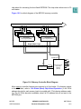
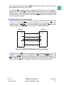
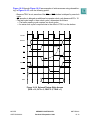
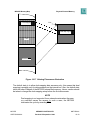
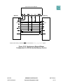
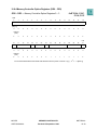
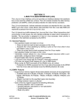
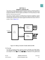
Each memory bank includes a variable block size of 32 Kbytes, 64 Kbytes and up to
4 Gbytes. Each memory bank can be selected for read-only or read/write operation.
The access to a memory bank can be restricted to certain address type codes for system protection. The address type comparison occurs with a mask option as well.
From zero to 30 wait states can be programmed with TA generation. Four byte-write
and read-enable signals (WE/BE(0:3)) are available for each byte that is written to
memory. An output enable (OE) signal is provided to eliminate external glue logic. A
memory transfer start (MTS) strobe permits one master on a bus to access external
memory through the chip selects on another.
The memory controller functionality allows MPC555-based systems to be built with little or no glue logic. A minimal system using no glue logic is shown in Figure 10-3. In
this example CS0 is used for the 16-bit boot EPROM and CS1 is used for the 32-bit
SRAM. The WE/BE[0:3] signals are used both to program the EPROM and to enable
write access to various bytes in the RAM.
Address
Address
CE
CE
OE
OE
CS0
OE
WE/BE[0:1]
Data
DATA[0:15]
[0:15]
EPROM
MPC555
Address
CS1
CE
WE/BE[0:3]
WE/BE[0:3]
W
[0:31]
Data
OE
SRAM
Figure 10-3 MPC555 Simple System Configuration
10.2 Memory Controller Architecture
The memory controller consists of a basic machine that handles the memory access
cycle: the general-purpose chip-select machine (GPCM).
MPC555
USER’S MANUAL
MEMORY CONTROLLER
Revised 15 September 1999
MOTOROLA
10-3