1
iSBC 80/05
SINGLE BOARD COMPUTER
HARDWARE
REFERENCE MANUAL
Manual Order Number: 9800483-03
1
Copyright© 1977, 1980 Intel Corporation
Intel Corporation, 3065 Bowers Avenue, Santa Clara, California 95051
I
PREFACE
This manual provides general information, installation, programming information, principles of operation, and service
information for the Intel SBC 80/05 Single Board Computer. Additional information is available in the following documents:
•
Intel MCS 85 User's Manual, part no. 121506.
•
Intel 8080/8085 Assembly LanKuaKe ProKramminK Manual, part no. 98-30 I.
•
Intel MULTIBUS Interj'acinK, Application Note AP-28.
111
CONTENTS
CHAPTER 1
GENERAL INFORMATION
Introduction
Description
System Expansion
System Software Development
Equipment Supplied
Equipment Required But Not Supplied
Specifica tions
CHAPTER 2
PREPARATION FOR USE
Introduction
Unpacking and Inspection
Installation Considerations
User-Furnished Components
Power Requirements
Cooling Requirements
Physical Dimensions
Component Configuration
RS232C Serial Input/Output
Line Driver/Receiver
Connector
TTL Level Serial Input/Output
Parallel Input/Output Ports
Input Port Terminators
Output Port Drivers
Read-Only Memory
Power Supply Filters
Alternative +5 V Input
Jumper Configuration
CPU Interrupts
TRAP Interrupt
RST 7.5 Interrupt
RST 6.5 and 5.5 Interrupts
Multibus Interrupts
Multibus Configuration
Signal Characteristics
Serial Priority Resolution
Parallel Priority Resolution
Single-Board Configuration
Peripheral Interfacing
Serial I/O Wiring
Parallel I/O Wiring
CHAPTER 3
PROGRAMMING INFORMATION
Introduction
Memory Addressing
iv
Page
I-I
I-I
1-2
1-3
1-3
1-3
1-3
Page
2-1
2-1
2-1
2-1
2-1
2-1
2-1
2-1
2-1
2-3
2-3
2-3
2-4
2-5
2-5
,2-5
2-5
2-5
2-5
2-6
2-6
2-6
2-8
2-9
2-9
2-9
2-9
2-16
2-16
2-16
2-16
2-17
Parallel I/O Section
I/O Register Addressing
Programming the Command Register (Port 00) .
Reading the Status Register (Port 00)
Port 01 Register
Port 02 Register
Port 03 Register
Timer Section
Serial I/O Communication
Interrupts
Timer Interrupts
TRAP Interrupts
CHAPTER 4
PRINCIPLES OF OPERATION
Introduction
Functional Description
Circuit Analysis
Initialization
Clock Circuits
Instruction Timing
Opcode Fetch Timing
Memory Read Timing
I/O Read Timing
Memory Write Timing
I/O Write Timing
Multiplexed Address/Data Bus
Multibus Interface
On-Board Memory
Read-Only Memory
Random Access Memory
On-Board I/O Ports and Timer
Register Addressing
Timer Addressing
Interrupts
Serial I/O Communication .
CHAPTER 5
SERVICE INFORMATION
Introduction
Service Diagrams
Service and Repair Assistance
I
3-1
3-1
3-2
3-2
3-2
3-2
3-2
3-3
3-4
3-6
3-6
3-6
Page
4-1
4-1
4-3
4-3
4-3
4-3
4-4
4-6
4-6
4-7
4-7
4-8
4-8
4-8
4-9
4-9
4-9
4-10
4-10
4-11
4-11
Page
5-1
5-1
5-1
Page
3-1
3-1
APPENDIX A
TELETYPEWRITER MODIFICATIONS
A-I
TABLES
Table Title
Specifica hons
......... .
User-Furnished and Installed Components
User-Furnished Connector Details
Power Requirements
Jumper-Selectable Options
Connector PI Pin Assignments
Multibus Signal Functions
SBC 80/05 Bus Interface AC Characteristics
SBC 80/05 Bus Interface DC Characteristics
Connector 11 Pin Assignments
Connector J2 Pin Assignments . . . . .
Page
Table Title
1-3
Parallel I/O and TTL Level Serial I/O
DC Characteristics
SBC 80/05 Memory Addresses
I/O Register Addresses . . .
Port 03 Programmable Modes
Baud Rates Vs Count Lengths
Serial Input Data Routine (Non-Interrupt
Driven)
........,..
Serial Output Data Routine (Non-Interrupt
Driven)
........,
Interrupt Vector Memory Locations
Timer Interrupt Routines
2-2
2-4
2-6
2-7
2-10
2-11
2-13
2-15
2-18
2-18
Page
2-19
3-1
3-2
3-3
3-4
3-4
3-5
3-6
3-7
ILLUSTRATIONS
Figure Title
SBC 80/05 Single Board Computer
CPU Interrupt Input Jumpers
Multibus Interrupt Jumpers
SBC 80/05 Bus Exchange Timing
SBC 80/05 Bus Control Timing
Serial Priority Resolution Scheme
Parallel Priority Resolution Scheme
RS232C Serial I/O Device Interface Cabling
TTL Level Serial I/O Device Interface Cabling
Command Register Format (Port 00).
Status Register Format (Port 00) . . . . .
Page
I-I
2-8
2-9
2-12
2-12
2-13
2-14
2-17
2-17
3-2
3-2
Figure Title
Timer Format
..... .
SBC 80/05 Block Diagram
Typical CPU Instruction Cycle
Typical Opcode Fetch Machine Cycle
Opcode Fetch Machine Cycle (With Wait)
Memory Read (or I/O Read) Machine Cycles
Memory Write (or I/O Write) Machine Cycles
SBC 80/05 Parts Location Diagram
SBC 80/05 Schematic Diagram
SBC 604 Schematic'Diagram
SBC 614 Schematic Diagram
Page
3-3
4-2
4-4
4-4
4-5
4-6
4-7
5-3
5-5
5-11
5-13
v/vi
CHAPTER 1
GENERAL INFORMATION
1-1. INTRODUCTION
The SBC 80/05 Single Board Computer, which is a member of Intel's complete line of SBC 80 computer products, is a computer system on a single printed-circuit
assembly. The SBC 80/05 includes a central processor
unit (CPU), system clock, random access memory{RAM),
read-only memory (ROM), one serial and three parallel
I/O ports, a programmable timer, priority interrupt and
Multibus control logic, and bus expansion buffers.
1-2. DESCRIPTION
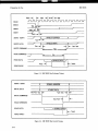
The SBC 80/05 Single Board Computer (figure 1-1) is
controlled by an Intel8085A CPU, which includes six 8bit general-purpose registers and an accumulator. The
six general-purpose registers may be addressedindividually or in pairs, which allows both single-precision and
double-precision operations. The minimum on board
execution time is 2.03 microseconds.
The 8085A CPU has a 16-bit program counter which
allows direct addressing of up to 65,536 bytes of memory. An external stack, located within any portion of
read/write memory, may be used as a last-in/first-out
storage area for the contents of the program counter,
flags, accumulator, and all six general-purpose registers.
A 16-bit stack pointer controls the addressing of this
external stack, which allows subroutine nesting that is
bounded only by the system memory size.
Two Intel 81ll-A4 RAM chips provide 256 bytes of
static read/write memory; an Intel 8155 combination
RAM/IO/Timer provides an additional 256 bytes of static
read/write memory. Two sockets are provided for installing up to 4K bytes of nonvolatile read-only memory
(ROM), which may be added in 2K byte increments
using Intel 2716 Ultraviolet Erasable and Reprogrammabie ROM's (EPROM's) or 8316E Masked ROM's.
Optionally, if only 2K bytes are required, ROM may be
added in lK byte increments using Intel 8708 EPROM's
or 8308 Masked ROM's.
Twenty-two programmable parallel I/O lines are implemented using the I/O ports of the Intel 8155 RAM/IO/
Timer. The system software is used to configure the I/O
lines in any combination of unidirectional input or output ports. The I/O interface may be customized to meet
specific peripheral requirements. In order to take full advantage of the large number of possible I/O configurations, sockets are provided for interchangeable I/O
(JIO PORTS)
(MULTIBUS CONNECTOR)
(NOT USED)
Figure 1-1. SBC 80/05 Single Board Computer
1-1
SBe 80/05
General Information
line drivers and terminators. Hence, the flexibility of
the I/O interface is further enhanced by the capability of
selecting the appropriate combination of optional line
drivers and terminators to provide the required sink
current, polarity, and drive/termination characteristics
for each application. The 22 programmable I/O lines
and single ground lines are brought out to a 50-pin edge
connector (J I) that mates with flat, woven, or round
cable.
The SBC 80/05 includes the resources for supporting
a variety of OEM system requirements. For those applications requiring additional processing capacity and the
benefits of multiprocessing (i.e., several CPU's and/or
controllers logically sharing systems tasks with communication over the Multibus), the SBC 80/05 provides full
bus arbitration control logic. This control logic allows up
to three bus masters (i.e., any combination of SBC 80/05.
SBC 80/20, DMA controller, diskette controller, etc.)
to share the Multibus in serial (daisy-chain) fashion or
up to 16 bus masters to share the Multibus using an external parallel priority resolving network.
The Multibus arbitration logic operates synchronously
with the bus clock, which is derived from the SBC 80/05,
or can be optionally generated by some other bus master. Data, however, is transferred via a handshake between the controlling master and the addressed slave
module .. This arrangement allows different speed controllers to share resources on the same bus, and transfers via the bus proceed asynchronously. Thus, the
transfer speed is dependent on transmitting and receiving
devices only. This design prevents slow master modules
from being handicapped in their attempts to gain control of the bus, but does not restrict the speed at which
faster modules can transfer data via the same bus. The
most obvious applications for the master-slave capabilities of the bus are multiprocessor configurations, highspeed direct memory access (DMA) operations, and highspeed peripheral control, but are by no means limited
to these three.
The Intel 8155 RAM/IO/Timer includes a programmable
14-bit interval timer, which is configured by software
to meet the system requirements. Whevener a given time
delay is needed, software commands to the timer select
the desired operating mode. The current contents (present count) of the timer counter and the timer mode
bits may be read at any time during system operation.
There are four timer operating modes:
a.
b.
1-2
Timer Out goes low during the second half of
count. Therefore, the count loaded in the Count
Length Register should be twice the timeout desired.
Timer Out remains high until the first half of the
count has been completed, and goes low for the
second half of the count. The count length is automatically reloaded when the terminal count is
reached.
c.
A single low pulse is generated upon reaching the
terminal count; this function is useful for generating real-time clocks.
d.
A Divide-by-N Counter generates a repetitive Timer
Out low pulse; a new pulse train is initiated every
time the terminal count is reached.
Serial I/O capability is provided through the Serial Input
Data (SID) and Serial Output Data (SOD) functions of
the CPU. These functions are controlled exclusively by
software through the execution of RIM and SIM instructions. The baud rate for the serial I/O interface is determined by the system time available for the execution of
serial I/O support software. Hence, the maximum baud
rate supported by the SBC 80/05 is solely dependent on
the overall system real-time software requirements. Serial
I/O signals are TTL compatible and sockets are provided
on the board for optional installation of RS232C line
drivers and receivers.
The SBC 80/05 provides jumper-selectable interrupts to
the four interrupt request inputs of the 8085 CPU (i.e.,
TRAP, RST 7.5, RST 6.5, and RST 5.5), each of which
generates a unique memory address. A jump (JMP) instruction at each of these addresses can provide the linkage to an interrupt handling subroutine for the appropriate interrupting device. All interrupts except TRAP
may be masked by software. The TRAP interrupt should
be used for conditions (such as a power-down sequence)
tha t require the immediate attention of the CPU. Caution
should be exercised when using the TRAP interrllpt in
conjunction with the maskable interrupts. For further
details, refer to Chapter 3 of this manual.
SBC 80/05 interrupts may originate from 12 sources.
One jumper-selectable interrupt request can be automatically generated by the programmable interval timer upon
completion of the selected function. Two jumper-selectable interrupt requests can be automatically generated
by the I/O ports section of the 8155 when Ports Oland
02 of the 8155 are programmed to operate in the
"latched and strobed" mode. (Refer to Chapter 3.) Nine
jumper-selectable interrupt request lines are available to
the user for direct interfaces to user-designated peripheral devices, one via the I/O edge connector and eight via
the Multibus. The 12 interrupt request lines may each be
selectively routed to any of four 8085A CPU interrupt inputs (i.e., TRAP, RST 7.5, RST 6.5, and RST 5.5) via
jumpers.
1-3. SYSTEM EXPANSION
Processing power, memory, and I/O capacity may be increased in SBC 80/05 based systems with single +5V
General Information
SBC 80/05
power by adding standard Intel expansion boards. High
speed integer and fltoating-point arithmetic capabilities
may be added by using the SBC 310 High-Speed Mathematics Unit. Memory for these systems may be expanded
using the SBC 094 4K Byte CMOS RAM board. Input/
output capacity may be increased by adding SBC 80
Digital I/O boards. In addition to' these expansion options, SBC 80/05 based systems equipped with multiple
voltages may be expanded with many memory and I/O
options. Memory may be expanded to 65,536 bytes by
adding user-specified combinations of RAM boards,
PROM boards, or combination boards. Input/output
capacity may also be increased by adding SBC 80 Analog
I/O boards. Mass storage may be added by selecting the
appropriate single or double-density diskette subsystem.
Modular expandable backplanes and card cages are available to support multiboard systems.
1-4. SYSTEM SOFTWARE DEVELOPMENT
Intel's high-level programming language, PL/M, is also
available as a resident Intel Microcomputer Development System option. PL/M provides the capability to
program in a natural, algorithmic language and eliminates the need to manage register usage or allocate memory. PL/M programs can be written in a much shorter
time than assembly language programs for a given application.
1-5. EQUIPMENT SUPPLIED
The following is supplied with the SBC 80/05 Single
Board Computer:
a.
Schematic diagram, dwg no. 2001600
1-6. EQUIPMENT REQUIRED BUT NOT
SUPPLIED
Because the SBC 80/05 is designed to satisfy a variety of
applications, the user must purchase and install only
those components required to satisfy his particular needs.
A list of components required to configure all the intended applications of the SBC 80/05 is provided in
table 2-1.
The development cycle of SBC 80/05 based products
may be significantly reduced using the Intellec Microcomputer Development System. The resident macroassembler, text editor, and system monitor greatly
simplify the design, development, and debug of SBC
80/05 system software. An optional Diskette Operating
System provides a relocating macroassembler, relocating
loader and linkage editor, and a Library Manager. A unique In-Circuit Emulator (ICE-85) option provides the
capability of developing and debugging software directly
on the SBC 80/05.
1-7. SPECIFICATIONS
Specifications of the SBC 80/05 Single Board Computer
are listed in table 1-1.
Table 1-1. Specifications
WORD SIZE
Instruction:
Data:
CYCLE TIME:
MEMORY ADDRESSING
On-Board ROM/EPROM:
On-Board RAM:
MEMORY CAPACITY
On-Board ROM/EPROM:
On-Board RAM:
Off-Board Ex pansion:
I/O ADDRESSING:
8, 16, or 24 bits.
8 bits.
2.03 !J.sec ±0.1 % for fastest executable instruction;
i.e., four clock cycles.
OOOO-OFFF.
3E00-3FFF.
4K bytes with Intel 8316E ROM's or 2716 EPROM's;
2K bytes with Intel 8308 ROM's or 8708 EPROM's.
5 J 2 bytes.
Up to 65K bytes (less on-board memory) in any combination
of RAM, ROM, and EPROM.
On-board I/O addressing of parallel I/O ports are as follows:
Port
Addtess
8155
8155815581558155 Timer 8155 Time
Command/ Port Port Port Low-Order High-Order
01 02 03
Byte
Byte
Status
00
01
02
03
04
05
1-3
General Information
SBC 80/05
Table 1-1. Specifications (Continued)
PARALLEL I/O CAPACITY:
22 programmable lines (from the three 8155 I/O ports);
can be expanded to 1102 programmable lines by
using optional SBC 80 I/O boards.
SERIAL I/O PORT:
SID and SOD functions of the 8085A CPU are used for serial
I/O communication controlled by software through
RIM and SIM instructions. Baud rate is determined by
system time available for serial I/O handling. On-board
timer may be used to greatly ease serial I/O timing requirements.
Four-level interrupt routed to B085A CPU interrupt inputs.
Each interrupt automatically vectors the processor
to a unique memory location.
INTERRUPTS:
Interrupt
Input
Memory
Address
Priority
Type
TRAP
RST 7.5
RST 6.5
RST 5.5
0024
003C
0034
002C
Highest
2nd
3rd
Lowest
Non-Maskable
Maskable
Maskable
Maskable
NOTE: Caution must be exercised in the use of the TRAP
interrupt when utilized concurrently with maskable
interrupts (i.e., RST 7.5, RST 6.5 and RST 5.5).
For further details, refer to Chapter 3.
TIMER
Input Freq. Reference:
Outputs:
122.88 kHz ±O.l % (8.14 JJ.sec period nominal).
Operating modes vs output frequencies and timing intervals:
Function
Programmable Pulse
Square Wave Rate Generator
Rate Generator
Programmable Strobe
Indication
Timer/Counter
Minimum
Maximum
8.14 JJ.sec
7.50 Hz
7.50 Hz
66.67 msec
61.44 kHz
61.44 kHz
8.14JJ.sec
133.33 msec
INTERFACE COMPATIBILITY:
All TTL compatible; sockets provided for RS232C line drivers
and receivers.
MULTIBUS CLOCK:
9.8 MHz ±0.1 % derived from on-board crystal; clock may be
generated externally.
POWER REQUIREMENTS:
DC power requirements depend on user-installed options. Refer
to table 2-2.
ENVIRONMENTAL REQUIREMENTS
Opera ting Tern pera ture:
Relative Humidity:
0 0 to 55 0 C (32 0 to 131 OF).
To 90% without condensation.
PHYSICAL CHARACTERISTICS
Width:
Height:
Thickness:
Weight:
30.48 em (12.00 inches).
17.15 em (6.75 inches).
1.27 em (0.50 inch).
340 gm (12 ounces).
1-4
CHAPTER 2
PREPARATION FOR USE
2-1. INTRODUCTION
2·5. POWER REQUIREMENTS
The chapter provides instructions for preparing the SBe
80/05 Single Board Computer for use in a multiple master bus system and for use in a single board environment.
It is advisable that the contents of Chapters 1 and 3 be
fully understood before beginning the configuration and
installation procedures con tained in this chapter.
Power requirements for the SBC 80/05 are listed in table
2-3. Note that the power requirements not only depend
on the intended application, but on the user-installed
EPROM type as well. Note also that filter capacitors
must be furnished and installed by the user if any power
supply other than a +5V supply is required.
2-6. COOLING REQUIREMENT
2-2. UNPACKING AND INSPECTION
Inspect the shipping carton immediately upon receipt for
evidence of mishandling during transit. If the shipping
carton is severely damaged or waterstained, request that
the carrier's agent be present when the carton is opened.
If the carrier's agent is not present when the carton is
opened and the contents of the carton are damaged,
keep the carton and packing material for the agent's inspection.
Por repairs to a product damaged in shipment, contact
the Intel Technical Support Center (see paragraph 5-3)
to obtain a Return Authorization Number and further
instructions. A purchase order will be required to complete the repair. A copy of the purchase order should be
submitted to the carrier with your claim.
The SBC 80/05 dissipates 196 gram-calories/minute
(0.79 BTU/minute) and adequate circulation of air must
be provided to prevent a temperature rise above 55 0 C
(131 0 p).
2-7. PHYSICAL DIMENSIONS
Physical dimensions of the SBC 80/05 are as follows:
a. Width:
b. Height:
c. Thickness:
30.48 cm (12.00 inches)
17.15 em (6.75 inches)
1.27 em (0.50 inch)
2-8. COMPONENT CONFIGURATION
It is suggested that salvageable shipping cartons and pack-
ing material be saved for future use in the event the product must be reshipped.
.2-3. INSTALLATION CONSIDERATIONS
Important installation and interfacing criteria for fabricating an SBC 80/05 computer-based system and for
using the SBe 80/05 in a single-board environment are
presented in following paragraphs.
Instructions for installing various components on the
SBC 80/05 to satisfy a particular configuration requirement are presented in following paragraphs. The following are recommended for installing those components that must be soldered in place:
a.
Ungar (or equivalent) soldering iron with a 40W
heating element and pencil-shaped tip.
b.
Multicore rosin flux 60/40 solder.
After the component is soldered in place, clean all
traces of flux from the soldered area using Freon TF
Degreaser (or equivalent).
2·4. USER-FURNISHED COMPONENTS
Because the SBC 80/05 IS designed to satisfy a variety of
applications, the user must purchase and install only
those components required to satisfy his particular needs.
A list of components required to configure all the intended applications of the SBC 80/05 is provided in
table 2-1. Table 2-2 lists alternative types and vendors of
the connectors referenced in table 2-1.
2-9. RS232C SERIAL INPUT/OUTPUT
The SBC 80/05 can employ RS232C or TTL level serial
I/O operation, but not both simultaneously. If RS232C
serial I/O operation is to be used, install the fine driver,
line receiver, and connector as described in following
paragraphs.
2·]
Preparation for Use
SBC 80/05
Table 2-1. User-Furnished and Installed Components
ITEM
NO.
ITEM
DESCRIPTION
USE
I
SBC 604
Modular Backplane and Cardcage. Includes four slots with
bus terminators. (See figure
5-3.)
Provides power inpu ts and
Multibus interface between
SBC 80/05 and three additional boards in a multiple
board system.
2
SBC 614
Modular Backplane and Cardcage. Includes four slots without bus terminators. (See figure 5-4.)
Provides four-board extension of SBC 604.
3
Connector (mates
with PI)
See Multibus connector details in table 2-2.
Power inputs and Multibus
interface. Not required if
(I) SBC 80/05 is installed
in an SBC 604/614 or (2)
if SBC 80/05 is used in a
single-board configuration
that needs +5V power only
(see item 6).
4
Connector (mates
with Jl)
See parallel I/O connector
details in table 2-2.
Interfaces parallel I/O devices and TTL level serial
I/O device to SBC 80/05.
5
Connector J2
Male and female connector
required. See table 2-2 for
description.
Interfaces RS232C or TTLlevel serial I/O device to
SBC 80/0~. (Either RS232C
or TTL level serial I/O can
be accommodated, but not
both.)
6
COJlnector J3
Male and female connector
req uired. See table 2 -2 for
description.
Provides aIternat,ive +5V
power input when SBC
80/05 is used in a singleboard configuration that
needs +5V power only.
(Refer to table 2-3.)
7
EPROM's or
ROM's
One or two each of one of
the following types of
EPROM's or ROM's:
Intel 2716 (2K x 8) or 8708
2-2
(1 K x 8) EPROM
On-board UV erasable
PROM's for program
development
Intel 8316E (2K x 8) or 8308
OK x 8) ROM
On-board masked ROM's
for dedicated program
Preparation for Use
SBC 80/0S
Table 2-1. User-Furnished and Installed Components (Continued)
ITEM
NO.
8
ITEM
RS232C line driver
RS232C line receiver
9
Line Driver
USE
DESCRIPTION
Transmitting and receiving
serial I/O data to and from
RS232C device.
Type: National DS1488 or
TI SN75188
Type: National DS1489 or
TI SN75189
Type
SN7403
SN7400
SN7408
SN7409
Requires two line driver
IC's for each parallel output port. (Requires only
one line driver IC for Port
03 if Port 03 is to be used
as control signals for Ports
01 and 02.)
Current
I,OC
I
NI
NI,OC
l6mA
l6mA
l6mA
l6mA
Types selected as typical;
I = inverting, NI = noninverting, and OC = open
collector.
10
I/O Terminators
220
SBC 901
-&
0
Capacitors
330
FV
SBC 902
11
Requires two 901 's or two
902's for each parallel input port. (Requires only
one 901 or 902 for Port 03
if Port 03 is to be used as
control signals for Ports 01
and 02.)
Intel SBC 901 Divider or
SBC 902 Pull-Up:
+5V
See table 2-3.
2-10. LINE DRIVER/RECEIVER. As specified in, table
2-1 (item 8), a line driver and a line receiver must be installed to accommodate RS232C serial I/O operation.
Refer to figure 5-1 and install a type 1488 line driver in
IC socket All. (Orient pin 1 of 1488 adjacent to capacitor C6.) Install a type 1489 line receiver in IC socket
AIO. (Orient pin 1 of 1489 adjacent to capacitor C5.)
2-11. CONNECTOR. As specified in table 2-1 (item 5),
connector 12 must be installed to interface the RS232C
serial I/O device to the SBC 80/05. Solder this 7-pinmale
0
Required only if power
supply other than +5V
supply is needed.
connector in position as shown in figure 5-1 (grid reference ZD3).
2-12. TTL LEVEL SERIAL INPUT/OUTPUT
The SBC 80/05 can employ RS232C or TTL level serial
I/O operation, but not both simultaneously. Provision is
made on connector Jl for interfacing the parallel I/O
ports and the TTL level serial I/O device. If using connector J 1 for both functions is impractical, connector 12
must be installed. Refer to table 2-1 (item 5). Solder
this 7-pin male connector in position as shown in figure
5-1 (grid refer'ence ZD3).
2-3
Preparation for Use
SBC 80/05
2-13. PARALLEL INPUT/OUTPUT PORTS
Parallel I/O Ports Oland 02 must be individually configured as either a dedicated input port or a dedicated
output port. Port 03 may also be configured as either a
dedicated input port or a dedicated output port, or used
as control signals for Ports Oland 02 when these ports
are to be used in the strobed input or strobed output
mode. For use as a dedicated output port, line drivers
(table 2-1, item 9) must be installed; for use as a dedicated input port, I/O terminators (table 2-1, item 10)
must be installed. The following six Ie sockets (two for
Table 2-2. User-Furnished Connector Details
Function
Parallel
I/O
Connector
(Jl)
Parallel
I/O
Connector
(Jl)
Parallel I
I/O
Connector
(Jl)
No. of
Pairsl
Pins
Centers
(Inches)
Connector
Type
25/50
0.1
Flat Crimp
25/50
0.1
Soldered
Vendor
Vendor
Part No.
Intel
Part No.
3M
AMP
Ansley
SAE
3415-0001
88083-1
609-5015
S06750 Series
102211-003
GTE Sylvania
Masterite
Micro Plastics
Viking
6ADOl-25-1A1-DD
NDD8GR25-DR-H-X
MP-0100-25-DP-I
102237-001
3KH25/JND5
3KH25/9JN5
25/50
0.1
Wire Wrap
Viking
TI
ITT Cannon
Multibus l
Connector
(PI)
43/86
0.156
Soldered
PCB Mount
Elfab
Viking
2KH43/9AMK12
Multibus 1.2
Connector
(PI)
43/86
0.156
Wire Wrap
No Ears
Edac
Elfab
337-086-0540-201
BW1562D43PBB
017
0.156
Wire Crimp
Molex'
Molex'
AMp·
AMp l •4
09-66-1071 male
09-50-7071 female
87194-6 male
3-87025-4 female
Molex 3 •s
Molex 3 •5
AMp4,5
AMp l .4.5
09-66-1021 male
09-50-7071 female
89194-1 male
2-87025-5 female
Serial
I/O
(J2)
Unregulated
+5V
(J3)
0/2
0.156
Wire Crimp
H421011-25
EC4A050AIA
NA
BS1562043PBB
102247-001
Notes:
'Connector heights are not guaranteed to conform to OEM packaging equipment.
2Wirewrap pin lengths are not guaranteed to conform to OEM packaging equipment.
JPin Part number is 08-50-0106; key part number is 15-04-0219.
4Pin part number is 87023-1; key part number is 87116-2.
5Connector J3 does not accept key.
6Connector numbering convention may not agree with board connector numbers.
2-4
102248-001
N/A
N/A
Preparation for Use
SBC 80/05
~ach port) are provided to accommodate the line drivers
and I/O terminators:
Parallel I/O
Port No.
01
02
03
IC Sockets
Figure 5-1
Grid Ref
A6,A7
A4,A5
A8,A9
ZD5, ZD4
ZD6, ZD5
ZD4, ZD4
If Port 03 is to be used as control signals for Ports 01 and
02, install a line driver in socket A8 and an I/O terminator in socket A9.
2·17. POWER SUPPLY FILTERS
Filter capacitors must be installed if a power supply other
than a +5V supply is required. Capacitors that must be
installed by the user are spec.ified in table 2-3. Refer to
figure 5-1 and install the capacitors as follows:
Component
RS232
Drivers
Intel 8708
EPROM's
Capacitors
Figure 5·1
Grid Ref
-12V
C26*
ZB5*
+12V
C7, C24*
ZD3, ZB8*
+12V
cn, C24*
ZC3, ZB8*
-5V
C12, C23*
ZD3, ZB8*
Supply
* Observe polarity as shown in figure 5-1.
2-14. INPUT PORT TERMINATORS. Refer to table 2-1
(item 10) and notice that each parallel input port requires either two Intel SBC 901 Divider IC's or two SBC
902 Pull-Up IC's. Plug terminators into the appropriate
IC sockets. Ensure that each IC is installed so that pin 1
is oriented toward connector J 1 on the upper edge of
the board.
2·15. OUTPUT PORT DRIVERS. Table 2-1 (item 9)
lists four typical types of IC's which may be selected as
line drivers depending on the user's application. Two
driver IC's are required for each dedicated output port.
Ensure that each IC is installed so that pin 1 is oriented
toward connector J 1 on the upper edge of the board.
2-18. ALTERNATIVE +SV INPUT
Connector 13 (table 2-1, item 6) provides an alternative, economical ;means of inputting +5V power to the
SBC 80/05. Note that connector 13 is to be installed
only if the SBC 80/05 is used in a single·board configuration (i.e., the Multibus is not required) and no power
other than +5V power is required. Install connector 13
as shown in figure 5-1 (grid reference B8). Piil 2 (adjacent to bus controller A 19) is the +5V input; pin 1 is
ground.
2·19. JUMPER CONFIGURATION
2-16. READ·ONLY MEMORY
Sockets are provided to accommodate either two Ep·
ROM's or two ROM's as specified in table 2·1 (item
7). Plug EPROM's or ROM's in IC locations A16 and
A17 (figure 5-1 grid coordinates C4). Ensure that each
EPROM or ROM is installed so that pin 1 is oriented toward connector J1 on the upper edge ofthe board. Refer
to paragraph 2-17 for installation of filter capacitors.
NOTE
If only one EPROM or ROM chip is being installed (i.e., a 1K or 2K configuration), install
the one chip in socket Al 7. Socket A 17 accommodates the lower addresses 0000·03FF for lK
chips and 0000-07FF for 2K chips.
The SBC 80/05 jumper·selectable options are listed and
described in table 2-4. Grid references are provided to locate each jumper on the parts location diagram (figure
5-1) and schematic diagram (figure 5-2). Grid references
to figure 5·2 are four alphanumeric characters; for ex·
ample, grid reference 3ZB3 signifies sheet 3 Zone B3.
Carefully study table 2·4 while making reference to figure 5-2 and configure each jumper (or jumper combi·
nation) as required. With the exception of jumper pad
W5 (CPU interrupts) and jumper pad W9 (Multibus in·
terrupts), the information presented in table 2·4 is con·
sidered adequate to properly configure the SBC 80/05
for your particular application. Clarification o·f jumper
pads W5 and W9 is presented in paragraphs 2-20 through
2-24.
2·5
SBC 80/0S
Preparation for Use
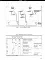
2-20. CPU INTERRUPTS
As described in table 2-4, jumper pad W5 is used for connecting selected interrupts to the CPU: TRAP, RST 7.5,
RST 6.5, and RST 5.5. The TRAP interrupt (highest
priority) is both edge and level sensitive and the R'ST 7.5
interrupt (second highest priority) is rising-edge sensitive. The RST 6.5 and RST 5.5 interrupts are both highlevel sensitive; RST 5.5 is the lowest priority. For purpose of examples, jumper pad W5 is illustrated in figure
2-1 ..
2-21. TRAP INTERRUPT. The TRAP interrupt, which
is not maskable, is jumpered at the factory to GND
(ground) to prevent the possibility of false interrupts from
being generated by noise spikes. Since this interrupt is
non-maskable, cannot be disabled by the program, and
has the highest interrupt, it may be used to detect catastrophic system errors such as a power failure or bus
failure. The logic for detecting such catastrophic system
errors must be developed by the system designer and
preferably input to the SBC 80/05 CPU via the Multibus interrupt line. (Refer to paragraph 2-24.)
2-22. RST 7.5 INTERRUPT. The RST 7.5 interrupt is
jumpered at the factory to the TMR (Timer) output of
the 8155. It is recommended that the jumper remain in
this position because the RST 7.5 interrupt is rising-edge
sensitive and the 8155 outputs a single ground-true pulse
when the termin.al count is reached. The trailing (rising)
edge of this pulse is used to trigger the RST 7.5 interrupt.
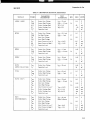
Table 2-3. Power Requirements
SUPPLY
MAXIMUM
CURRENT
COMMENTS
ICC = 1.8A
With no ROM/EPROM or parallel I/O ports.
ICC = 2.65A
With two Intel 2716 EPROM's (or 8316E ROM's) and
six Intel SBC 901 or SBC 902 I/O terminators in the
low state. See table 2-1 (items 7 and 10).
-5V ±5%
IBB = 90 rnA
Required only when Intel 8708 EPROM's (or 8308
ROM's) are used instead of 2716's (or 8316E's). See
table 2-1 (items 7 and 11) and notes below.
+12V ±5%
IDD = 137 rnA
Required for Intel 8708 EPROM's (or 8308 ROM's)
and RS232C line driver and receiver. See table 2-1
(items 7, 8 and 11) and notes below.
-12V ±5%
IAA =23mA
Required only for RS232C line driver and receiver.
See table 2-1 (items 8 and II) and notes below.
+5V ±5%
Notes:
1.
If power supply other than +5V supply is required, the user must furnish and install the
following capacitors (refer to paragraph 2-17 for details):
-5V supply: C12, C23
+12V supply: C7, Cll, C24
-12V supply:
C26
2.
Capacitor specifications are:
C7, Cll, C12: ceramic, disc, O.OIJlF +80 -20%, 25V, Sprague C092B250CI037 or equivalent.
C23, C24, C26: tantalum, 22 JlF ±20%, 15V, Sprague 150D226X90 15B2 or equivalent.
3.
2-6
Instaliation procedures are gIven in subsequent paragraphs.
Preparation for Use
SBC 80/0S
Table 2-4. Jumper-Selectable Options
JUMPER
WI
W6
FIG. S-l FIG. S-2
GRID
GRID
REF
REF
ZC6
ZC7
3ZB3
2ZDS
DESCRIPTION
WI is used in conjunction with W6 to define four modes of resolving bus
contention, three of which are for use in multiple master systems. According
to the selected mode, the SBC 80/0S can gain access to the Multibus as follows:
Mode 1:
Mode 2:
Mode 3:
Mode 4:
Can request Multibus as needed (multiple master system).
Always requesting Multibus (lowest priority in a multiple
master sytem).
Programmable override of Multibus (multiple master system). During an override condition, the SBC 80/05 will
not relinquish bus control until programmed to do so.
Always overriding Multibus (single master system).
Jumper positions for configuring each of these four modes are as follows
(for example, to configure W I for Mode 3, remove jumpers from positions A-D
and B-C and install jumper only in position A-B):
Jumper
Mode 1
Mode 2
WI
*A-D and
*B-C
*A-B
*A-D and
*B-C
B-C
W6
W2
W3
W4
WS
ZC6
lZB7
Mode 3
A-B
(only)
A-B
Mode 4
B-C
(only)
A-B
*B-C:
PC3 is used as a Port 03 input/output bit or as a Port 02 interrupt signal
depending on how the 81SS is programmed. If the Port 02 strobed input
or output mode is used, the INTR PORT 02 signal must be connected
to the CPU interrupt input via jumper pad WS.
A-C:
Connects INTR PORT 02 to interrupt an alternative system master via
jumper pad W9.
ZC3
ZC3
3ZA7
3ZA7
* W3loaded with jumper block accommodates Intel 2716 EPROM's or 8316E
ROM's; W4loaded with jumper block accommodates Intel 8708 EPROM's or
8308 ROM's. If 2716's or 8316E's are used, leave jumper block installed in W3;
if 8708's or 8308's are used, remove jumper block from W3 and reinstall in W4
(refer to paragraphs 2-16 and 2-17).
ZC8
lZB6
Priority jumper pad for connecting selected interrupts to CPU. The CPU has three
maskable interrupts (RST 5.5, RST 6.5, and RST 7.5) and one nonmaskable
interrupt (TRAP). These four interrupts are characterized as follows (refer to
paragraphs 2-20 through 2-24 for jumper selectable inputs):
TRAP
RST 7.5
RST 6.5
RST S.5
Highest Priority
2nd
3rd
Lowest Priority
Edge and level sensitive.
Rising-edge sensitive.
High-level sensitive.
High-level sensitive.
W7
ZB7
2ZCS
* A-B:
Routes Bus Clock signal BCLK/ to the Multibus. Remove this jumper
only if some other module is used to generate BCLK/.
W8
ZB7
2ZCS
*A-B:
Routes Constant Clock signal CCLK/ to the Multibus. Remove this jumper
only if some other module is used to generate CCLK/.
2-7
Preparation for Use
SBC 80/05
Table 2-4. Jumper Selectable Options (Continued)
JUMPER
FIG. 5-1 FIG. 5-2
GRID
GRID
REF
REF
DESCRIPTION
W9
ZB7
1ZC7
Interfaces 80/05 with the eight interrupt request lines (INTO/ through INT7 f)
on the Mu1tibus. (Refer to paragraph 2-24 for details.)
W10
ZB8
2ZD3
*A-B:
Routes Bus Priority Out signal BPRO/ to the Multibus. Remove this
jumper only in a multiple master device system employing a parallel
priority bus resolution scheme. Refer to paragraph 2-28.
WI I
ZBs
3ZDs
*A-B:
Routes ground-true Chip Enable signal to Intel 8155 chip. Do not
remove jumper from this position.
W12
ZC4
3ZB3
*A-B:
PC4 is used as a Port 03 input/output bit or as a Port 02 Buffer Full
status bit depending on how the 8155 is programmed.
A-C:
W13
ZD8
1ZCS
PC4 used as an RS232C Reader Control output signal.
*A-B:
Routes output of.5 counter to Xl (dock) input of CPU. Do not remove
jumper from this position.
*Jumper installed in this position at the factory.
2-23. RST 6.5 AND 5.5 INTERRUPTS. The RST 6.5
and RST 5.5 interrupts are level sensitive and may be
driven from the following interrupt sources:
a. PORT 1 and PORT 2 (from the on-board 8155)
b. EXT I (from an external source via connector J 1)
c. Multibus interrupt lines (refer to paragraph 2-24).
As shown in figure 2-1, two of these interrupt sources
may be jumpered to the J ""Id K inputs of an OR-gate,
which in turn may be jump~.·ed to either the RST 6.5 or
RST 5.5 interrupt. When this feature is used, the interrupting source must be identified by executing a polling
subroutine.
Q..
<t
a:
GND
EXT 1
PORT 1
In
~
ID
A
B
In
In
~
IF'Q~S
GO
0
H
,..:
D
E
0 CPU
0 f>
(
C
I_
N
~
a: a:
b [ ~~
J
K
0
()
L
M
W5
0
N
0
P
0
R
0
S
BUS INTRS
NOTES:
1.
TRAP AND RST 7.5 INTERRUPTS
ARE FACTORY JUMPER ED TO
GND (GROUND) AND TMR (TIMER),
RESPECTIVELY.
2.
FOR BUS INTRS INTERFACE WITH
W9, SEE FIGURE 2-2.
Figure 2-1. CPU Interrupt Input Jumpers
2-8
Preparation for Use
SBC 80/0S
2-24. MULTIBUS INTERRUPTS
The eight Multibus interrupt lines (INTO/ through INT7 f)
are applied to one side of jumper block W9. (See figure 2-2.) Four of these interrupts may be jumpered and
applied (via the inverters) to jumper pad W5 for distribution to the selected CPU interrupts. Refer to table
2-4 and figure 2-2 and note that W2 may be jumpered
and applied to W9 through the inverter. This allows the
INTR PORT 02 to be connected to an alternative system master by the selected Multibus interrupt line.
Always turn off the power supply before installing the board in or removing the board from
the backplane. Failure to observe this precaution can result in damage to the board.
2-26. SIGNAL CHARACTERISTICS
As shown in figure I-I, connector P I provides the means
of interfacing the SBC 80/05 to the Multibus. Pin
assignments for connector P I are listed in table 2-5; the
functions of the bus signals are described in table 2-6.
2-25. MULTIBUS CONFIGURATION
AC characteristics of the SBC 80(05 bus interface are
presented in table 2-7 and figures 2-3 and 2-4. DC
characteristics are specified in ta ble 2-8.
For system applications, the SBC 80(05 is designed for
installation in a standard Intel SBC 604(614 Modular
Backplane and Cardcage. (Refer to table 2-1, items I and
2.) Alternatively, the SBC 80/05 may be interfaced to a
user-designed system backplane by means of an 86-pin
connector. (Refer to table 2-1, item 3.) Bus signal
characteristics and methods of implementing a serial or
parallel priority resolution scheme for resolving bus contention in a multiple master system are described in following paragraphs.
r
I
I
I
2-27. SERIAL PRIORITY RESOLUTION
In a multiple master system, bus contention can be resolved in an SBC 604 Modular Backplane and Card cage
by implementing a serial priority resolution scheme as
shown in figure 2-5. Due to the propagation delay of the
BPRO/ signal path, this scheme is limited to a maximum
of three devices (masters) capable of acquiring and con-
So--+-----------oc
BUS
INTRS
Rn--+---------oc
W2 (REFER TO TABLE 2-4)
r--,
P 0--+------0<
IA
NO-+---O~
c
I
B"O+-
? I
L. __ ..J
I
L __ --.J
PARTOFW5
(SEE FIGURE 2-1)
F
o
G
ABC
0
E
BUS INTERRUPTS
HJ KLMNP
.......
.......
(Q
.......
.......
l-
IZ
l-
I-
.....
Z
'<:t
Z
.......
N
l-
U'l
Z
Z
---I- ---l-0
M
~
v
Z
INTR PORT 02
W9
........
~
I-
Z
I
MULTIBUS
Figure 2-2. Multibus Interrupt Jumpers
2-9
Preparation for Use
SBC 80/0S
trolling the Multibus. In the configuration shown in figure 2-5, the SBC 80/05 installed. in slot 12 has the
highest priority and is able to acquire the Multibus at
any time because its BPRN / input isena bled (tied to
ground) through jumpers Band N on the SBC 604 backplane. (See figure 5-3.) If the master in slot 12 desires
control of the Multibus, it drives its BPROj output high
and inhibits the BPRN/ input to all lower-priority mod-
ules. When finished using the bus, the 12 master pulls its
BPRO/ output low and passes control to the 13 master.
If the 13 master does not desire to control the bus at
this time, it pulls its BPRO/ output low and passes control to the J4 master.
The serial priority scheme can be implemented in a userdesigned system bus if the chaining of BPRN/ and BPRO/
signals are wired as shown in figure 5-3.
Table 2-5. Connector PI Pin Assignments
PIN*
1
2
3
4
5
6
7
8
9
10
II
12
13
14
1St
16
17
18
19
20
21
22
23
24
25
26
27
28
29
30
31
32
33
34
35
36
37
38
39
40
41
42
43
*
t
2-10
SIGNAL
GND
GND
+5 VDC
+5 VDC
+5 VDC
+5 VDC
+12VDC
+12VDC
-5 VDC
-5 VDC
GND
GND
BCLK/
IN IT/
BPRN/
BPRO
BUSY/
BREQ/
MRDC/
MWTC/
10RC/
IOWC/
XACK/
CCLK/
INT6/
INT7/
INT4/
INT5/
INT2/
INT3/
INTO/
INTI/
ADRE/
FUNCTION
{ Ground
{
Power input
{ Power input
{ Power input
{ Ground
Bus Clock (9.8304 MHz)
System Initialize
Bus Priority In
Bus Priority Out
Busy
Bus Request
Memory Read Command
Memory Write Command
I/O Read Command
I/O Write Command
Transfer Acknowledge
Constant Clock (9.8304 MHz)
Interrupt request
Interrupt request
Interrupt request
Interrupt request
Interrupt request
Interrupt request
Interrupt request
Interrupt request
Address bus
line
line
line
line
line
line
line
line
6
7
4
5
2
3
0
1
All unassigned pins are reserved (do not use).
Connect BPRN / to ground in single master systems.
PIN*
SIGNAL
44
45
46
47
48
49
50
51
52
53
54
55
56
57
58
59
60
61
62
63
64
65
66
67
68
69
70
71
72
73
74
75
76
77
78
79
80
81
82
83
84
85
86
ADRF/
FUNCTION
,
ADRCf
ADRD/
ADRA/
ADRB/
ADR8/
ADR9/
ADR6/
ADR7/
ADR4/
ADR5/
ADR2/
ADR3/
ADRO/
ADRI/
DAT6/
DAT7/
DAT4/
DAT5/
DAT2/
DAT3/
DATO/
DATI/
GND
GND
-12 VDC
-12 VDC
+5 VDC
+5 VDC
+5 VDC
+5 VDC
GND
GND
Address bus
Data bus
,
{ Ground
{ Power input
{ Pow,"npu!
{ Ground
Preparation for Use
SBC 80/0S
Table 2-6. Multibus Signal Functions
SIGNAL
FUNCTIONAL DESCRIPTION
ADRO/-ADRF /
Address. These 16 address lines transmit the address of the memory location
or I/O port to be accessed. ADRF / is the most-significant bit.
BCLK/
Bus Clock. Used to synchronize bus control circuit on all master boards.
BCLK/ from the SBC 80/05 has a period of 101.72 nanoseconds
(9.8304 MHz frequency) with a 35-65 percent duty cycle.
BPRN/
Bus Priority In. Indicates to a particular master board that no higher priority
master board is requesting use of the bus. BPRN/ is synchronized with
BCLK/.
BPRO/
Bus Priority Out. In serial (daisy chain) priority resolution schemes, BPRO/
must be connected to the BPRN/ input of the master board with the
next lower bus priority.
BREQ/
Bus Request. Used with a parallel bus priority resolution scheme to indicate
that a particular master board requires use of the bus for one or more
data transfers. BREQ/ is synchronized with BCLK/.
BUSY/
Busy. Indicates that the bus is in use and prevents all other master boards
from gaining control of the bus. BUSY/is synchronized with BCLK/.
CCLK/
Constant Clock. Provides a clock signal of constant frequency (9.8304 MHz)
for use by system boards. CCLK/ from the SBC 80/05 coincides with
BCLK/ and has a period of 101.72 nanoseconds with a 35-65 percent
duty cycle.
DATO/-DAT7/
Data. These eight bidirectional data lines transmit and receive information
to and from the addressed memory location or I/O port. DAT7/ is the
most-significant bit.
INIT/
Initialization. Resets the entire system to a known internal state.
INTO/-INT7 /
Interrupt. These eight lines are used for system interrupt requests.
10RC/
1/0 Read Command. Indicates that the address of an I/O port is on the
system address lines and that the output of that port is to be read
(placed) onto the system data lines.
10WC/
I/O Write Command. Indicates that the address of an I/O port is on the
system address lines and that the contents on the system data lines
are to be accepted by the addressed port.
MRDC/
Memory Read Command. Indicates that the address of a memory location
is on the system address lines and that the contents of that location
are to be read (placed) onto the system data lines.
MWTC/
Memory Write Command. Indicates that the address of a memory location
is on the system address lines and that the contents on the system
data lines are to be written onto that location.
XACK/
Transfer A cknowledge. Indicates that the addressed memory location or I/O
port has completed the specified read or write operation. That is, data.
has been placed onto or accepted from the system data lines.
2-11
SBC 80/05
Preparation for Use
tBCY
BCLK/
BREQ/
------~~
ADROi- ADRFI
..- - - - - - - - - - - - - - - - I/~--------J
r
--7
I
u-
tBS ~I.-:"'I
tpPD
BPRN/
BUSYI
--1
===<:BY
T
-~
u
u
----
--
~ \l-I'-----------------X' --- ----
n
X
STABLE ADDRESS
tAS ~.'--,--~-~'-'-=..;;;.;;;....:...=..::....;..o=:.----'
7
'----~
?'tDS ~'''-:-t--S.:....T-A-B-''L.:....E-D-:-CT-DA----j---IXf-'---tA-H-' t :
WRITE DATA
-J
WRITE COMMAND
READ COMMAND
==:J:Jr-----t\..~====~~tC~D~=====!!j~------
READ DATA
~'I
READ XACKI
I
STABLE DATA
~ tXKO
-------------~--~\'---------_~/~-------------
Figure 2-3. SBC 80/0S Bus Exchange Timing
ADRO/- ADRF/
WRITE DATA
___~X~___S~T~A~B~L~E~A~D~D~R~E~S_S_ _ ___IX~__________
------.xI
tAS' tDS
WRITE COMMAND
READ COMMAND
READ DATA
--.j
I
X~-------
STABLE DATA
t-~
tAH, tDH
'AH, toH
-1
~
j.-
I~~----------
\'-------~I
I~---------------
Ic_
\'_____--'X STABLE DATA('
t XKO_
READ XACKI
\
Figure 2-4. SBC 80/0S Bus Control Timing
2-12
I
Preparation for Use
SBC 80/05
HIGHEST
PRIORITY
MASTER
LOWEST
PRIORITY
MASTER
J2
15
J3
15
BPRNt
BPROt p..!L
SBC 80/05
J4
15
BPRNt
BPROt
~
BPROt
SBC501
I
B
I
N
--
--------
DISKETTE
CONTROLLER
-------- -- - - - - - - - -
-
""---
l....-
C(
I
~
16
SBC 201
DIRECT MEMORY
ACCESS
CONTROLLER
r- -
BPROt AND BPRNt PINS
NOT USE D BY NON·
MASTER S.
BPRNt
M~
IL _____________________
_
\J
-- l
E C
H
L~
K
I
~:
SBC 604
BACKPLANE
(BOTTOM)
---------------~
Figure 2-5. Serial Priority Resolution Scheme
Table 2-7. SBC 80/05 Bus Interface AC Characteristics
OVERALL
PARAMETER
WRITE
READ
MIN. MAX. MIN.
(ns)
(ns)
(ns)
MAX. MIN.
(ns)
(ns)
MAX.
(ns)
t As
50
50
50
Address Setup Time to Command
tAH
50
50
50
Address Hold Time from Command
tos
50
50
Data Setup Time to Command
tOH
50
50
tCY
508
Data Hold Time from Command
CPU Cycle Time
510
tco
690
690
Command Width
t CS1 ,2
475
475
Command Separation
980
tCS3
980
tCS4
tppo
t XKO
0
65
t BWS
35
OC
t BS
15
tOBY
t pNO
t BCY
tBW
tiNT
REMARKS
OESCR IPTIO N'
63
0
65
0
65
ASSUME BUS AVAILABLE
"o
R. .
R . .' }
Write to Write
Command Separation
Read to Write
Command Separation
Write to Read
Parallel Priority Resolution Delay
BREQ/ to BPRN/
Override
Mode
XACK Turn Off Delay
Bus Clock Low or High Intervals
Supplied by system.
BPRN to BCLK Setup Time
30
BCLK to Busy Delay
20
BPRN to BPRO Delay
100
102
Bus Clock Period (BCLK)
35
74
3000
{
Bus Clock Low or High Intervals
Initialization Width
From SBC 80/05 wften
properly term inated
After all voltages
I
have stablized,
'See figures 2·3 and 2-4'for timing diagrams.
2-13
SBC 80/05
Preparation for Use
HIGHEST
PRIORITY
J3
J2
~
~
BPRN/
p!!!.
() B
BREal p!8
A(
J5
~ BPRN/
BPRN/
(NOTE)
(NOTE)
(NOTE)
r - - - - - - - - - :
~
BPRNI
(NOTE)
BREal
LOWEST
PRIORITY
J4
BREal
~
- - - - - - - - - - - - - - - - -
L _ """" ________
;> C
~
D
I) E
Fe:>
_ _ _ _ _ _ _ _ _ _______
BREa/
- - - r--, sac 604
>H
~
BUS
PRIORITY
RESOLVER
P
f"
BREa/INPUTS
FROM MASTERS
IN SBe 614
7 R
I
6 0
R
5 I
T
4 Y
P
R 7 PI
o 61.-..
R
I 5,",
T
Y 4
,. 3 E D 31.-..
2
r-<
BPRN/ OUTPUTS
TO MASTERS
IN SBe 614
N E 2
C C
0
o
1
D D
0 E E 0
R R
NOTE: REFER TO IMPORTANT INFORMATION PROVIDED IN PARAGRAPH 2-28.
Figure 2-6. Parallel Priority Resolution Scheme
2-14
G1
:
BACKPLANE
___ ...J (BOTTOM)
t
L-....c
~
Preparation for Use
SHe 80/05
Table 2-8. SBC 80/05 Bus Interface DC Characteristics
SIGNALS
SYMBOL
PARAMETER
DESCRIPTION
TEST
CONDITIONS
VOL
VOH
ILH
ILL
CL *
Output Low Voltage
Output High Voltage
Output Leakage High
Output Leakage Low
Capacitive Load
IOL=32rnA
IOH = -5.2 rnA
Vo = 2.4V
VO=O.4V
VOL
VOH
VIL
Vm
Output Low Voltage
Out High Voltage
IOL = 59.5 rnA
IOH = -3 rnA
IlL
1m
CL*
Input Currernt at Low V
Input Current at High V
Capacitive Load
VOL
VOH
CL *
Output Low Voltage
Output High Voltage
Capacitive Load
IOL = 3.2 rnA
lOB = -0.4 rnA
VOL
VOH
CL *
Output Low Voltage
Output High Voltage
Capacitive Load
IOL = 20 rnA
IOH = -0.4 rnA
BUSYI
(OPEN COLLECTOR)
VOL
CL
Output Low Voltage
Capacitive Load
IOL = 20 rnA
CCLKI
VOL
V OH
CL *
Output Low Voltage
Output High Voltage
Capacitive Load
IOL = 60 rnA
IOH = -3 rnA
VOL
VOH
VIL
V IH
Output Low Voltage
Output High Voltage
Input Low Voltage
Input High Voltage
IOL = 50 rnA
IOH = -10 rnA
ADRO/ - ADRF I
BCLKI
BPROI
BREQI
DATOI - DAT71
INITI
(SYSTEM RESET)
Input Low Voltage
Input High Voltage
MIN
MAX
0.4
2.4
40
-40
18
0.5
2.7
0.8
2.0
-0.5
VIN =0.45V
VIN = 5.25V
40
15
0.45
2.4
10
0.45
UNITS
V
V
jJ.A
jJ.A
pF
V
V
V
V
rnA
jJ.A
pF
V
V
pF
10
V
V
pF
0.45
20
V
pF
0.5
V
V
pF
2.4
2.7
15
0.6
2.4
0.95
2.0
V
V
V
V
IlL
Input Current at Low V
V IN = 0.45V
-0.25·
rnA
ILH
Output Leakage High
ILL
CL*
Output Leakage Low
Capacitive Load
VO =5.25V
VO= 0.45V
100
100
18
1;.A
jJ.A
pF
VOL
VOH
V1L
VIH
Output Low Voltage
Output High Voltage
IOL = 44 rnA
Open Collector
0.4
V
0.8
V
IlL
IIH
CL *
Input Current at Low V
Input Current at High V
Capacitive Load
Input Low Voltage
Input High Voltage
2.0
VIN = O.4V
V IN = 2.4V
-1.0
V
rnA
0,7
18
rnA
pF
2-15
Preparation for Use
SBC 80/0S
Table 2-8. SBC 80/0S Bus Interface DC Characteristics (Continued)
PARAMETER
DESCRIPTION
TEST
CONDITIONS
SIGNALS
SYMBOL
INTO/-INT7 /
XACK/
VIL
VIH
IlL
IIH
CL*
Input Low Voltage
Input High Voltage
Input Current at Low V
Input Current at High V
Capacitive Load
VOL
VOH
ILH
ILL
CL*
Output Low Voltage
Output High Voltage
Output Leakage High
Output Leakage Low
Capacitive Load
MRDC/, MWTC/
10RC/,IOWC/
MIN
MAX
0.8
2.0
-004
20
18
VIN = OAV
VIN = 2.7V
10L = 32 rnA
IOH=-2mA
Vo = 5.25V
Vo = 0.45V
UNITS
V
V
rnA
JlA
pF
0045
V
V
100
100
15
JlA
JlA
204
pF
*Capacitive load values are approximations.
2-28. PARALLEL PRIORITY RESOLUTION
A parallel priority resolution scheme allows up to 16
masters to acquire and controi the Multibus. Figure 2-6
illustrates one method of implementing such a scheme
for resolving bus contention in a system containing
eight master modules installed in an SBC 604/614. In
this example, the priority encoder is a Texas Instruments 74148 and the priority decoder is an Intel 8205.
Input connections to the priority encoder determine the
bus priority, with input 7 having the highest priority and
input 0 having the lowest priority. Here, the J3 master
has the highest priority and the J4 master has the lowest
priority.
IMPORTANT: In a parallel priority resolution scheme,
the BPRO/ output signal must be disabled on all master
modules. On the SBC 80/05, disable the BPRO/output
signal by removing jumper WID. If a similar jumper is not
provided on the other master modules to disable the
BPROI output signal, either clip the IC pin that supplies
the BPROI output signal to the Multibus or cut the trace.
2-29. SINGLE-BOARD CONFIGURATION
........
CAUTION
~
...................~
Always turn off the power supply before
connecting or disconnecting power leads. Failure to observe this precaution can result in
damage to the board.
If the SBC 80/05 is used in a single-board configuration
and power other than +5V is specified in table 2-2, an
86-pin connector must be provided to input power to
the board. A description of the connector is given in
table 2-1 (item 3) and power job connections are listed
in table 2-5. Assuming that all the necessary components
have been installed and that the jumpers have been
2-16
appropriately configured, proceed with interfacing peripheral equipment to the SBC 80/05 as described in following paragraphs.
2-30. PERIPHERAL INTERFACING
An RS232C or a TTL level serial I/O device (but not
both) and three TTL level parallel I/O ports may be interfaced to the SBC 80/05 as described in following
paragraphs. If a Teletype Model ASR-33 is to be used
as the RS232C serial I/O device, it must be modified as
described in Appendix B.
2-31. SERIAL I/O WIRING
An RS232C serial I/O device must be interfaced to the
SBC 80/05 via connector 12. A TTL level serial I/O device may be interfaced to the SBC 80/05 via connector
J I or 12. Pin assignments for connectors J 1 and 12 are
listed in tables 2-9 and 2-10, respectively.
Figure 2-7 illustrates the cabling required for interfacing connector 12 to an RS232C serial I/O device.
Notice that the transmission path from J2 to the RS232C
device connector should be limited to 15.25 meters (50
feet.) In an extremely noisy electrical environment,
twisted-pair wires may be used in a fashion similar to
that shown in figure 2-8. For interfacing with teletypewriters and other 20 rnA current loop equipment, an
Intel SBC 530 Teletypewriter (TTY) Adapter (or equivalent) is required. (Refer to Appendix B.)
Figure 2-8 illustrates the cabling required for interfacing connector 12 to a TTL level serial I/O device; the
de characteristics of the TTL serial I/O port are given iii.
table 2-11. Notice in figure 2-8 that the transmission
path from J2 to the TTL device connector should be
SBC 80/0S
Preparation for Use
limited to 3 meters (10 feet). The TTL level serial I/O
device can also be interfaced to the SBC 80/05 via
connector J l. (Refer to paragraph 2-32 and table 2-9.)
The individual wires connected to J I for TTL level
serial I/O should be two pair of wires of the cable used
for interfacing the parallel I/O channels.
2-32. PARALLEL I/O WIRING
The SBC 80/05 interfaces to the three parallel I/O ports
via connector J l. Using 50-conductor cable and a mating
connector for 11 (table 2-1, item 4), interface the para-
MOLEX 09-50-7071
RS232C CONNECTOR
RS232C SERIAL OUT DATA (SOD/)
1
TO
SBC 80/05
J2
3
RS232C SERIAL IN DATA (SID/)
2
2
RS232C READER CONTROL
3
6
GROUND
4
TO P30F
SBC530
TTY ADAPTER
7
V-
V50 FEET (15.25 METERS) MAXIMUM
Figure 2-7. RS232C Serial I/O Device Interface Cabling
MOLEX 09-50-7071
~ DENOTES TWISTED PAIR
CONNECTOR
AS REQUIRED
~
5
TTL LEVEL SERIAL IN DATA (SID/)
r::
,/
TO
SBC80/05
4
J2
6
[.../-
GROUND
"
1"--'
-
TO TTL LEVEL
SERIAL I/O
DEVICE
r'\. GROUND
~( TTL LEVEL SERIAL OUT DATA (SOD/)
"--'
/-
10 FEET (3 METERS) MAXIMUM
Figure 2-8. TTL Level Serial I/O Device Interface Cablina
2-17
Preparation for Use
SBC 80/05
llel I/O ports to the appropriate pins on J I as listed in
table 2-9. The transmission path from the SBC 80/05 to
the parallel I/O ports should be limited to 3 meters (10
feet) maximum. The dc characteristics of the SBC 80/05
parallel I/O ports are presented in table 2-11. The following bulk cable types (or equivalent) are recommended
for interfacing with the parallel I/O ports (assuming 25
line pairs are used):
a. Cable, flat, 50-conductor, 3M 3306-50.
b. Cable, flat, 50-conductor (with ground plane), 3M
3380-50.
c. Cable, woven, 25-pair, 3M 3321-25.
Table 2-9. Connector J1 Pin Assignments
PIN
I
2
3
4
5
6
7
8
9
10
11
12
13
14
15
16
17
18
19
20 1
21
221
23
24
25
FUNCTION
GND
Port 02
GND
Port 02
GND
Port 02
GND
Port 02
GND
Port 02
GND
Port 02
GND
Port 02
GND
Port 02
GND
Port 03
GND
Port 03
GND
Port 03
GND
Port 03
GND
PIN
bit 7
bit 6
bit 5
bit 4
bit 3
bit 2
bit I
bit 0
bit 3
bit 2 (Port 01 Strobe)
bit I (Port 01 Buffer Full)
bit 0
26 1
27
28 1
29
30
31
32
33
34
35
36
37
38
39
40
41
42
43
44
45
46
47
48
49
50
FUNCTION
Port 03 bit 4 (Port 02 Buffer Full)
GND
Port 03 bit 5 (Port 02 Strobe)
GND
TTL level SOD/ (Serial Out Data)
GND
TTL level SID / (Serial In Data)
GND
Port 01 bit 7
GND
Port 01 bit 6
GND
Port 0 I bit 5
GND
Port 01 bit 4
GND
Port 01 bit 3
GND
Port 0 I bit 2
GND
Port 0 I bit 1
GND
Port 01 bit 0
GND
EXT INTR I / (External Interrupt I)
1. These pins are used as control signals when Ports 01 and 02 are used in the latched and strobe mode.
2. Pin numbers refer to board connector pins only, they are not necessarily the same on the mating connectors.
Table 2-10. Connector 12 Pin Assignments
PIN
1
2
3
4
FUNCTION
Reserved
TTL level SOD; (Serial Out Data)
TTL level SID I (Serial In Data)
GND
PIN
5
6
7
FUNCTION
RS232C level RDR CTL (Reader Control)
RS232C level SID; (Serial In Data)
RS 232C level SOD; (Serial Out Data)
~
1. Pin numbers refer to board connector pins only, they are not necessarily the same on the mating connectors.
2·18
Preparation for Use
SBC 80/05
Table 2-11. Parallel I/O and TTL Level Serial I/O DC Characteristics
SIGNALS
8155
DRIVER/
RECEIVER
TTL SID/
TTL SOD/
SYMBOL
PARAMETER
DESCRIPTION
TEST
CONDITIONS
VOL
VOH
VIL
Vm
Output Low Voltage
Output High Voltage
Input Low Voltage
Input High Voltage
IOL = 2.0 rnA
IOH = ~400 /lA
IlL
IIH
CL*
Input Current at Low V
Input Current at High V
Capacitive Load
VIN = 0.45
VIN= 5.0
VIL
Vm
IlL
IIH
Input
Input
Input
Input
VOL
VOH
Output Low Voltage
Output High Voltage
Low Voltage
High Voltage
Current at Low V
Current at High V
MIN
MAX
UNITS
0.45
V
V
V
V
2.4
0.8
2.0
Vcc5
10
10
18
0.5
-- 2.0
V
V
rnA
50
/lA
0.5
V
2.0
VIN = 0.50
VIN = 2.7
IOL = 20 rnA
IOH = -1.0 rnA
2.7
/1A
/1A
pF
V
*Capacitive load value is approximate.
2-19/2-20
CHAPTER 3
PROGRAMMING INFORMATION
3-1. INTRODUCTION
read is attempted from an illegal address, erroneous data
will be returned; if a write is attempted to an illegal address, the da ta byte is lost.
This chapter lists the SBC 80/05 on-board memory
address assignments; provides programming details for
the parallel 110 section, timer section, and serial 110
port; and describes the 8085A CPU interrupt structure.
The 8085A CPU instruction set is provided in Appendix
A; a complete description of programming with Intel's
assembly language is given in 8080/8085 Assembly Language Programming Manual, part no. 98-310.
When power is initially applied to the SBC 80/05, or
when a reset is otherwise initiated, the CPU program
counter (PC) and instruction register are set to zero.
Thus, the CPU initially fetches the instruction in location 0000. It is expected that this location in ROM/
EPROM will reference a user-defined routine such as an
automatic bootstrap loader for a paper tape reader, magnetic type, disc, etc.
3-2. MEMORY ADDRESSING
3-3. PARALLEL I/O SECTION
Addresses for on-board read/write memory (RAM) and
read-only memory (ROM or EPROM) are given in table
3-1. Note in table 3-1 that the address space listed for
ROM/EPROM depends on how the SBC 80/05 is configured by the user.
When on-board memory is addressed, a Memory Advanced Acknowledge (MEM AACKf) signal is generated
which allows the CPU to operate at maximum speed.
When system memory is addressed, the CPU must first
gain control of the Multibus and then wait for a Transfer Acknowledge (XACKf) to be received from the system memory device.
If a non-existent memory location is addressed, the CPU
will hang up in a wait state until reset. It should be noted
in table 3-1 that it is possible to configure ROM/EPROM
such as to create illegal addresses. If an illegal address is
used, a MEM AACK/ signal is generated as described for
a legal address and the CPU will continue executing. If a
Table 3-1.
TYPE
ROM
or
EPROM
RAM
The Intel 8155 includes two 8-bit parallel I/O ports
(Port 01 and Port 02) and one 6-bit parallel I/O port
(Port 03). Each of these three ports can be individually
hardware configured as either an input port or an output
port (but hot both). Port 03 can be programmed to allow
Port 0 I and Port 02 to operate in a handshake mode
with their associated input or output device. In this case,
Port 03 must be specifically hardware configured to perform this function and cannot be used as an input port
or as an output port.
3-4. I/O REGISTER ADDRESSING
The I/O section consists of a Command/Status (C/S) register and one register for each of the three I/O ports.
Addresses for these four registers are provided in table
3-2.
SBC 80/0S Memory Addresses
CONFIG
LEGAL ADDRESSES
ILLEGAL ADDRESSES
One 8308/8708 chip
Two 8308/8716 chips
0000-03FF
0OOO-07FF
0400-07FF
One 2716/8316E chip
Two 2716/8316E chips
0OOO-07FF
OOOO-OFFF
0800-0FFF
N/A
3EOO-3FFF
N/A
3-1
SBC 80/05
Programming Information
Table 3-2. 110 Register Addresses
AD,
Register
Bits
I/O Address
Command/Sta tus
Port 01
Port 02
Port 03
LSB of Timer Count
MSB of Timer Count
Unused
Unused
R
8
8
6
8
8
00
01
02
03
04
05
06
07
AD6
ADS AD4 AD3 AD2 AD1 ADo
·lXlTIMER\INT~l
02
-
02JINTRIINTEI 01:1NTj
BF 02
01
BF 01
I
I
PORT 02 BUFFER FULL/EMPTY
(INPUT/OUTPUT)
~
The Command register can be altered at any time by
performing an I/O write to location 00. The specific
meaning of each register command bit is shown in figure 3-1.
,
I
~E~~
I
..
DEFINESPORTD'l
J
ENABLE PORT 01}
INTERRUPT
L -_ _ _ _ _ _ _ _ _ _ _ ~:;EBAL:U~RT
02
00 <=AlT1
11 = ALT 2
01 "ALT3
10" ALI 4
1 = ENABLE
0" DISABLE
OPERATION.
01 = STOP - NOP IF TIMER HAS NOT STARTED:
STOP COUNTING IF TIMER IS RUNNING
10= STOP AFTER TC-STOPIMMEDIATElY
AFTER PRESENT Te IS REACHED iNOP
IF TIMEA HAS NOT STARTED).
'1
=
Figure 3-2. Status Register Format (Port 00)
3-7. PORT 01 REGISTER
The Port 0 I register can be programmed to be either an
input port or an output port depending on Command
register bit O. (See figure 3-l.) Also, depending on the
Command, this port can operate in either the basic input/output mode or strobed mode depending on the alternative (ALT) mode programmed for Port 03. (Refer
to paragraph 3-9.)
0= INPUT
1 c OUTPUT
r- 00 '" NOP _ DO NOT AFFECT COUNTER
'-----I~ TIMER COMMAND -
PORT 02 INTERRUPT ENABLED
TIMER INTERRUPT (THIS BIT
IS LATCHED HIGH WHEN
TERMINAL COUNT IS
REACHED, AND IS RESET TO
LOW UPON READING CIS
REGISTER OR STARTING
NEW COUNT,)
DEFINES PORT 02
DEFINES PORT D3{
..
PORT 01 BUFFER FULl/EMPTY
(INPUT/OUTPUT)
PORT 02 INTERRUPT REQUEST
The Command register consists of eight I-bit latches.
Four bits (0 - 3) define the mode of Port 01 and Port
02, two bits (4 - 5) enable or disable the Port 01 and
Port 02 interrupts (in the strobed input/output mode),
and two bits (6 - 7) define the programmable timer command. (Refer to paragraph 3-10.)
Pl
PORT 01 INTERRUPT REQUEST
PORT 01 INTERRUPT ENABLE
3-5. PROGRAMMING THE COMMAND REGISTER
(PORT 00)
ITM2 TM,I IE 21 IE 11 P321 P3, i P2
~
START _ LOAD MODE AND CNT LENGTH
AND START IMMEDIATELY AFTER
3-8. PORT 02 REGISTER
The Port 02 register can be programmed to be either an
input port or an output port depending on Command
register bit l. (See figure 3-l.) Also, depending on the
Command, this port can operate in either the basic input/output mode or strobed mode depending on the alternative (ALT) mode programmed for Port 03. (Refer
to paragraph 3-9.)
LOADING (IF TIMER IS NOT PRESENTLY
RUNNING)' IF TIMER IS RUNNING. START
THE NEW MODE AND CNT LENGTH
IMMEDIATEL Y AFTER PRESENT Te
IS REACHED.
Figure 3-1. Command Register Format (Port 00)
3-6. READING THE STATUS REGISTER (PORT 00)
The Status register consists of seven I-bit latches. Bit 0-5
define the status of the ports and bit 6 defines the
status of the timer. The contents of the Status register
can be obtained at any time by performing an I/O read
to location 00. The format of the Status register is presented in figure 3-2.
3·2
3·9. PORT 03 REGISTER
The Port 03 register can be programmed as an input
port, output port, or as control signals for Port 01 and
Port 02 depending on the hardware configuration and
Command register bits 2 and 3. Figure 3-1 shows that
bits 2 and 3 specify four alternative modes for Port 03:
ALT I, ALT 2, ALT 3 and ALT 4. As noted in table 3-3
for ALT 3 mode, bits 0 - 2 are control bits for Port 01.
and bits 3 - 5 depend on the user's jumper-selected options.
Programming Information
SBC 80/0S
Table 3-3. Port 03 Programmable Modes
PORT 03 BIT
0
I
2
3
4
5
ALT I
Input
Input
Input
Input
Input
Input
Port
Port
Port
Port
Port
Port
ALT2
ALT 3
Output Port
Output Port
Output Port
Output Port
Output Port
Output Port
Port 0 I Interrupt
Port 0 I Buffer Full
Port 01 Strobe
Note I
Note 2
Note 3
ALT4
Port
Port
Port
Port
Port
Port
01
01
01
02
02
02
Interrupt
Buffer Full
Strobe
Interrupt
Buffer Full
Strobe
Notes:
1.
2.
3.
If W2 is in position B-C, bit 3 is output bit.
If WI2 is in position A-B, bit 4 is output bit; if W12 is in position A-C, bit 4 is RS232C Reader
Control (RDR CTL) signal.
If WI is in position A-B (only) and W6 is in position A-B, bit 5 is used to provide the programmable bus override mode; i.e., the SBC 80/05 will not relinquish the Multibus until Port 03 bit
5 is cleared. If the override function is not jumpered, bit 5 is not functional.
3-10. TIM ER SECTION
I/O
ADDRESS
04
The timer is a l4-bit down-counter that counts the
122.88-kHz timer (clock) input and outputs either a
square wave or a pulse when the terminal count (TC) is
reached. The timer output must be connected by the
user to the selected CPU interrupt via a jumper wire.
The timer includes a 16-bit register for holding the count
length (14 bits) and the operating mode (2 bits). The I/O
address for the low-order byte (least-significant bits of
count length) and high-order byte (most-significant bits
of count length and timer mode) is 04 and 05, respectively. Figure 3-3 shows the timer format and I/O addresses.
The timer I/O addresses serve a dual purpose. During a
I/O Write operation, the count length (bits 0 - 13) and
mode (bit 14 - 15) are loaded into the 16-bit register;
during an I/O Read operation, the present count (the
count at the time of the I/O Read operation) and the
mode bits are read. To ensure that the correct count is
read, it is preferable to stop counting, read the counter,
and then reload the counter and continue counting.
I
LSB OF CNT LENGTH
I/O
ADDRESS
05
I
TIMER
MODE
o
0
o
MSB OF CNT LENGTH
OUTPUT LOW DURING SECOND HALF OF
COUNT. (SEE NOTE.)
SQUARE WAVE OUTPUT; I.E., THE PERIOD
OF THE SQUARE WAVE EQUALS THE COUNT
LENGTH PROGRAMMED WITH AUTOMATIC
RELOAD AT TERMINAL COUNT.
o
SINGLE PULSE OUTPUT UPON TC BEING
REACHED.
By connecting the counter output to the RST 7.5 input
of the CPU, the CPU can be interrupt driven at the baud
rate desired for serial I/O communication. The count
lengths'required for various baud rates are given in table
3-4. Timer interrupt routines are presented in paragraph
3-13.
AUTOMATIC RELOAD; I.E., SINGLE PULSE
OUTPUT EVERY TIME TC IS REACHED.
NOTE:
In case of an asymmetric count (e.g •• 15).
output will be high during larger half of count.
Figure 3-3. Timer Format
3·3
SBC 80/0S
Programming Information
Table 3-4. Baud Rates Vs Count Lengths
BAUD RATE
DECIMAL
COUNT
4800
2400
1200
600
110
75
ERROR/FRAME
1.6%
0.4%
0.4%
0.1%
0.01%
0.01%
26
51
102
205
1117
1638
3-11. SERIAL I/O COMMUNICATION
Tables 3-5 and 3-6, respectively, provide examples of
serial input and serial output routines using the SID and
SOD instructions of the BOB5A CPU. Both routines,
which provide programmed timing loops at 2400 baud,
operate in the non-interrupt driver mode. The examples
are included for illustration purposes only and are not
intended to demonstrate the optimum way to program
the serial I/O port.
Table 3-S. Serial Input Data Routine (Non-Interrupt Driven)
FUNCTION: CIWAIT
INPUTS: NONE
OUTPUTS: NONE
CALLS: WAIT
DESCRIPTION: THIS ROUTINE WAITS FOR AN INPUT FROM THE CONSOLE BY READING
THE SID INPUT LINE. WHEN IT DETECTS A START BIT, IT THEN READS
THE INPUT CHARACTER AND RETURNS TO THE PLM CALLING PROGRAM WHEN THE INPUT CHARACTER IS A oW'.
CIWAIT:
BEGIN:
NEXT:
CHKW:
MVI
MVI
RIM
ANI
JZ
MVI
CALL
RIM
ANI
JZ
DCR
JZ
MVI
CALL
RIM
ANI
ORA
RRC
MOV
JMP
MOV
CPI
JNZ
RET
B,OOH
C,08H
; CLEAR OUT CHARACTER STORAGE REGISTER
; SET COUNT REGISTER
80H
BEGIN
D,IBH
WAIT
; CHECK FOR START BIT
; CONTINUE LOOKING UNTIL FOUND
; SET-UP DELAY
80H
BEGIN
C
CHKW
D,38H
WAIT
; CHECK FOR VALIDITY OF START BIT
80H
B
; CHECK REG ISTER A BIT 7
; LOAD PREVIOUS BITS INPUT INTO A
B,A
NEXT
A,B
28H
CIWAIT
; STORE DATA IN B REGISTER
; DECREMENT COUNT REGISTER
; CHECK TO SEE IF INPUT CHARACTER IS A oW'
; SET-UP DELAY
; COMPARE CI TO COMPLEMENT OF oW'
FUNCTION: WAIT
DESCRIPTION: ACCEPTS DATA IN THE D REGISTER WHICH DETERMINES THE NUMBER
OF TIMES THE LOOP WILL BE EXECUTED. THE LOOP INVOLVES TWO
INSTRUCTIQNS OR 14 CLOCK STATES.
WAJ.T:
DCR
JNZ
RET
3-4
D
WAIT
Programming Information
SBC 80/0S
Table 3-6. Serial Output Data Routine (Non-Interrupt Driven)
FUNCTION CO:
INPUTS: ACCEPTS A BYTE OF DATA IN THE C REGISTER OR FROM MEMORY
LOCATION SPECIFIED BY H&L REGISTERS.
OUTPUTS:
OUTPUTS SERIAL DATA VIA THE SOD LINE TO CONSOLE.
CALLS:
WAIT
DESCRIPTION: CO ACCEPTS AN ASCII BYTE FROM THE PLM SYS4 PROGRAM DIRECTLY
OR FROM THE MESOUT ROUTINE WHICH IS INVOKED BY THE PLM
SYS4 PROGRAM. IT FIRST OUTPUTS THE START BIT, THEN SEVEN
DATA BITS FOLLOWED BY TWO STOP BITS. THE PROPER DURATION
BETWEEN SOD OUTPUTS IS DETERMINED BY THE VALUE PASSED TO
THE WAIT ROUTINE VIA THE D REGISTER.
CO:
Ll:
L2:
MVI
MVI
SIM
MVI
CMP
JNZ
MOV
CMA
MOV
JMP
MOV
CMA
A,OCOH
E,07H
MOV
ANI
MVI
CALL
B,A
OFFH
D,34H
WAIT
L3
D,36H
WAIT
A,B
JMP
DELAY:
L3:
MVI
CALL
MOV
RRC
MOV
ORI
ANI
SIM
DCR
JNZ
MVI
CALL
MVI
SIM
MVI
CALL
RET
; SET UP FOR START BIT INSTRUCTION
; SET COUNTER FOR NUMBER OF DATA BITS
; BEGIN START BIT
A,OOH
C
L1
A,M
B,A
L2
A,C
B,A
40H
OCOH
; IF DATA IN C, DON'T LOOK IN MEMORY
; GET DATA FROM MEMORY
; GET DATA IN C REGISTER
; COMPLEMENT DATA (A I IN THE ACC WILL
PUT A 0 ON THE RS232 LINE)
; STORE IN B REGISTER
; DUMMY INSTRUCTION FOR TIMING DELAY
; SET-UP D REGISTER FOR TIME DELA Y (2400 BAUD)
; SET-UP D REGISTER FOR TIME DELA Y (2400 BAUD)
;
;
;
:
PUT LSB INTO BIT 7 FOR SIM INSTR
STORE DATA IN B REGISTER
PUT A '1' IN BIT 6 FOR SIM INSTR
MASK ANY OTHER BITS-AFFECT RSTS
E
DELAY
D,38H
WAIT
A,40H
; DECREMENT COUNT REGISTER
; CONTINUE OUTPUT FOR 7 DATA BITS
; SET-UP D REGISTER FOR DELA Y (2400 BAUD)
D,76H
WAIT
; SET-UP TWO STOP BIT DELAY (2400 BAUD)
; SET-UP A REGISTER FOR STOP BITS
FUNCTION: WAIT
DESCRIPTION: ACCEPTS DATA IN THE D REGISTER WHICH DETERMINES THE NUMBER
OF TIMES THE LOOP WILL BE EXECUTED. THE LOOP INVOLVES TWO
INSTRUCTIONS OR 14 CLOCK STATES.
WAIT:
DCR
D
JNZ
WAIT
RET
3-S
SBC 80/0S
Programming Information
Table 3-6. Serial Output Data Routine (Non-Interrupt Driven) (Continued)
FUNCTION: MESOUT
INPUTS: CHARACTER STRING DATA IN MEMORY SPECIFIED BY B&C REGISTERS.
OUTPUTS: POINTER ADDRESS IS LOADED IN H&L REGISTERS.
CALLS: CO
DESCRIPTION: THE PLM PROGRAM CALLS MESOUT WITH AN ADDRESS PARAMETER
PLACED IN THE BAND C REGISTERS. MESOUT LOADS THIS
ADDRESS INTO THE HAND L REGISTERS AND THEN CALLS THE
CO ROUTINE WHICH WILL OUTPUT THE ASCII DATA LOCATED IN
MEMORY SPECIFIED BY THESE REGISTERS. MESOUT WILL THEN
INCREMENT H&L AND CONTINUE TO CALL CO UNTIL A ZERO IS
FOUND IN MEMORY.
MESOUT:
LOOP:
H,B
D,C
C,OOH
CO
MOV
MOV
MVI
CALL
INX
MOV
ORI
JNZ
RET
H
A,M
OOH
LOOP
INDICATE TO CO THAT DATA IS IN MEMORY
; GET ADDRESS OF NEXT CHARACTER IN STRING
CHECK FOR END OF STRING
CONTINUE UNTIL ZERO FOUND IN MEMORY
3-12. INTERRUPTS
3-14. TRAP INTERRUPTS
The SBC 80/05 CPU includes four vectored interrupts:
TRAP, RST 7.5, RST 6.5, and RST 5.5. Jumpers may be
installed to allow interrupts from parallel I/O Ports 01
and 02, the programmable timer, one or more devices via
the Multibus, or an external source. Each of the three
RST inputs (7.5,6.5, and 5.5) has a programmable mask;
TRAP is not maskable. The priority and vector location
for each of these restart interrupts are given in table 3-7.
There are special considerations that must be made when
the TRAP interrupt is used. The fact that the TRAP interrupt is non-maskable can present problems in at least
two areas.
3-13. TIMER INTERRUPTS
Timer interrupt routine examples are presented in table
3-8. These examples include a timer initialization, which
is performed as part of the main program; a routine to
service an RST 7.5 interrupt; and a subroutine to save
the state of the machine upon being interrupted and to
restore the state of the machine after servicing the interrupt. These examples are included for illustration purposes only and are not intended to demonstrate the optimum way of programming these functions.
Table 3-7. Interrupt Vector Memory Locations
INTERRUPT
VECTOR
LOCATION
PRIORITY
TRAP
RST 7.5
RST 6.5
RST 5.5
24
3C
34
2C
Highest
2nd
3rd
Lowest
3-6
Interrupt driven systems often contain parameters that
must be modified only within critical regions. A critical
region can be roughly defined as a section of code that
once begun must complete execution before it or
another critical region that corresponds to the same
system parameter(s) can be executed. A TRAP interrupt
handler cannot safely alter such parameters either directly or indirectly by causing the execution of procedures or tasks that may alter such parameters.
If the hardware generates a TRAP interrupt on power up
or power fail, the system must be able to process the
TRAP interrupt before it is completely initialized. It
should also take into account that an interrupt routine
that runs with interrupts disabled can still be interrupted
by a TRAP.
Because of these considerations, it is recommended that
the TRAP interrupt only be used for system startup
and/or catastrophic error handling.
Programming Information
SBe 80/0S
Table 3·8. Timer Interrupt Routines
MAIN PROGRAM - INITIALIZES THE 8155 COUNTER AND STARTS THE
COUNT BEFORE CONTINUING WITH ITS OTHER ROUTINES. THIS PROGRAM
SETS THE TIME TO COUNT 122 TIMER-IN PULSES BEFORE OUTPUTTING A TIMER PULSE THAT WILL GENERATE AN INTERRUPT.
USING MODE 3, THE TIMER WILL AUTOMATICALLY RELOAD
AND BEGIN ANOTHER COUNTDOWN.
MVI
OUT
MVI
OUT
MVI
SIM
EI
MVI
OUT
A,7CH
4
A,OCOH
5
A,18H
; OUTPUT LSB OF COUNT LENGTH
; OUTPUT MSB AND TIMER MODE
; UNMASK RESTART INTERRUPTS
; ENABLE PROCESSOR INTERRUPTS
A,OCOH
0
; START TIMER COUNTDOWN
MAIN PROGRAM CONTINUES
END MAIN PROGRAM
FUNCTION: INTR 75
DESCRIPTION: WHEN A RST 7.5 IS GENERATED BY THE 8155 (DETERMINED BY
THE MAIN PROGRAM), THIS ROUTINE STORES THE STATUS WORD
AND THEN INCREMENTS A COUNT VARIABLE. IT MAY THEN CALL
A REAL TIME COUNT AND DISPLA Y ROUTINE WHICH INCREMENTS
VARIABLES FOR MILLISECONDS, SECONDS, ETC., AT THE PROPER TIME.
FINALLY, THE INTERRUPT ROUTINE WILL RESET RST 7.5, RESTORE
PROCESSOR STATUS WORD, AND ENABLE INTERRUPTS BEFORE RETURNING TO THE MAIN PROGRAM.
ORG
003CH
COUNT
EQU
PUSH
PUSH
PUSH
PUSH
PSW
B
D
H
; SAVE STATE OF MACHINE
LXI
INR
CALL
MVI
SIM
H,COUNT
M
RTC
A,lOH
; LOAD H&L WITH LOCATION OF COUNT
; INCREMENT THE COUNT
; CALL REAL TIME COUNT AND DISPLAY ROUTINE
(NOT SHOWN)
; RESET RST 7.5
POP
POP
POP
POP
EI
RET
H
D
B
PSW
; RESTORE STATE OF MACHINE
00
; SET TIMER DELAY
SAVE:
INTR75:
RSTORE:
3·7
CHAPTER 4
PRINCIPLES OF OPERATION
4-1. INTRODUCTION
This chapter provides a functional description and a circuit analysis of the SBC 80/05 Single Board Computer.
The circuit analysis is presented with the assumption
that the reader has access to the Intel MCS 85 User's
Manual, part no. 98-366, which describes in detail the
Intel 8085A Microprocessor (CPU) and the 8155 RAM/
10/Timer.
4-2. FUNCTIONAL DESCRIPTION
As shown in figure 4-1, the SBC 80/05 is composed of
the following functional blocks:
a. Clock Generator (including power-up reset).
b. CPU (including interrupt control).
c. Bus Interface (address bus' drivers, data bus drivers,
and bus controller).
d. Random Access Memory (RAM).
e. Read-Only Memory (ROM/EPROM).
f. Serial I/O Interface.
g. Parallel I/O Interface (including programmable
timer).
Crystal controlled Clock Generator A3 provides a stable
time base for the SBC 80/05 as well as for the Multibus.
The Clock Generator also generates a pawer-up reset
signal to initialize the entire system to a known internal
state.
The 8-bit parallel CPU, which is the heart of the system,
performs all the system processing functions and generates the address and control signals required to access
memory and I/O ports. The CPU multiplexes the 8-bit
data bus and the lower eight bits of the address bus.
During the first part of the machine cycle, the lower
eight address bits on the address/data bus are latched
into Demultiplexer A 18 and RAMOO/Timer A 15. During
the remainder of the machine cycle, the bus is used for
memory and I/O data transfers. The CPU responds to
interrupt requests originating from jumper-selectable
sources. As shown in figure 4-1, these interrupt requests may be generated by the on-board timer and
parallel I/O ports, by one or more devices via the Multibus, or by an external source.
The Bus Interface allows the SBC 80/05 to use a system
bus that is common to other master devices (e.g., CPU's
and DMA controllers), thus allowing system memory and
I/O devices to be shared on a priority basis. The primary element of the Bus Interface is Bus Can troller A 19,
which operates synchronously with the bus clock
(BCLKj) and consists of the following functional sections:
a. Bus arbitration logic to resolve bus contention in
multiple master systems.
b. Timing logic, initiated by the bus arbitration logic,
to ensure adequate setup and hold times for the address and data placed on the Multibus; also generates read/write control signals.
c. Output drive logic for driving the bus memory and
I/O command (control) lines.
When the SBC 80/05 gains control of the Multibus to
perform a write operation, the Bus Controller gates
the device address and data onto the Multibus and issues a Write command. In performing a read operation, the Bus Controller gates the device address onto
the Multibus and issues a Read command. Operations
between the CPU and the on-board memory and I/O
ports do not require the Multibus. Notice in figure 4-1
that the data bus drivers are bidirectional and the address bus drivers are unidirectional. This allows the SBC
80/05 full control of the Multibus but prevents other
modules from accessing the SBC 80/05 memory and I/O
ports.
The SBC 80/05 provides 512 eight-bit words of static
Random Access Memory (RAM). Two Intel 8111-A4
devices provide 256 words in locations 3EOO-3EFF.
The Intel 8155 RAM/IO/Timer provides 256 eight-bit
words of static RAM in locations 3FOO-3FFF. This 512
word RAM storage area requires neither refreshing nor
clock inputs, thereby providing the CPU immediate access to the addressed location.
Two IC sockets are provided to allow the user to install
either 2K or 4K bytes of Read Only Memory (ROM).
The user may install two Intel 2716 (2K x 8) or 8708
OK x 8) ultraviolet erasable and reprogrammable ROM's
(EPROM's) for program development or install two Intel 8316E (2K x 8) or 8308 OK x 8) masked ROM's
containing a dedicated program. Depending on the type
of ROM or EPROM installed, the address locations are
0000-07FF (two IK x 8-bit chips) or OOOO-OFFF (two
2K x 8-bit chips).
The Serifll I/O Interface is accomplished via the Serial
Input Data (SID) and Serial Output Data (SOD) pins on
the CPU. Data on the SID line is loaded into the CPU by
a RIM instruction; data on the SOD line is set or cleared
by a SIM instruction. Data buffers are provided for TTL
level interface. Sockets are provided for the installation
of level converters for RS232C interface.
SBC 80/0S
Principles of Operation
'9~M
MH,
~
t
I
--1'--_A"_,2_. . I. - - - - - - - - - - - - - - - - - - - - - - - - - - - = = = - - - = = - - < - - I
~v rD~ d~
~. ~~:""~
~i.
W
~~ A8.~A~M~-=AB~F----=_~------~A~D~D=RE~S~S~BU~S~-~~---~
>-~
V--
A'51-------="~"=------~f1 ~
RESET
DEMUX
8086A
AlB
ADO-
1/'--=--:---:---,..1\,
AD1
~
........
~~
01'-
D01
018
DOS
RESET
ALE~
_RESETI
393216 MHz
'---'-'--'--'-----+1 eLK
-+
ABO-AB7
m
~
)
A~:"O
t--
3EOO·
IN 1+2)
---/~~OT~E1(~ ~ ~
j:t':'
DBO-DB7
3E
~ RO~~~~ I
: :
l,---"
DATA BUS
'-------:,.--:::-----'
•
'-___,---'''1,
t
,. .
BIDIRECTIONAL
DATA BUS
t A- g:~~ '\
DRIVERS
\......-------. /
I'-__---=~"---="=-------_____---=="==":...,/
-~
~
v
IN/OUT
CONTROL BUS
. - - - - - - - 1 TRAP
, - - - - - + 1 R5T5.5
, - - - - - 1 R5T 6.5
~
~
elK OUT
+1.96608 MHz
'-----I
BUS
CONTROLLER
A19
CONTROL
ADO·AD7
BPRN/
BPRO/
Mise CONTROL
ALE
,,-
RESET/-----4INITI
BCLK/
A,4
ExT
INTERRUPT
/ ' PORT 01
'-______________
r----,
A6 A7
2I...J:
<:
8
,'<,.-------+v'
PORT 02
<
PORT 03
TO/FROM
INTERRUPT
SELECT
INTO/·
INnl ---"-
<,,-----,V
I
~:ORALLEL '.....----------.,.,liL 'NO~E
___
PORTS
--j<.:2'-i::~: ~:i~~
r---j
r-- - -,
?
A4. A6
I'NOTEZ)
PAo-7
NOTES:
1.
8
~
PII>-7
~
;; AU. </'-_L_-_-_-_.J_-fJ'-,,'" PCG-O
I 'NoTE 21 I ~
L - __ ..J
Ie SOCKETS ONLY, USER MUST INSTALL
2716 (or 8708) EPROM', OR 8318E (Of 83081
ROM'..
V
2.
.,. .
RAM/TomMER
A15
(NOTE 41
1
4.
8716/8316E: OOO().QFFF
8708/8308: OOOO-07FF
IC SOClETS ONLY. USER MUST INSTALL DRIVERS
tSN7400. 7408, ETC.) OR TERMINATORS liNTEl
SSC 901 OR SBC 9021.
IC SOCKETS ONLY. USER MUST INSTALL RS232C
DRIVER/RECEIVER.
A15 RAM ADDRESSES ARE lFO().3FFf.
Figure 4-1. SBC 80/05 Block Diagram
The Parallel 110 Interface consists of three general purpose ports provided by the Intel 8155 RAM/IO/Timer.
Each of the three ports can be programmed to be either
an input port or an output port. One of the three ports
(Port 03) can be programmed to be status pins, thus
allowing the other two ports (Ports Oland 02) to operate
in a handshake mode. The I/O portion of the 8155 contains four internal registers - one register for command
and status and one data register for each of the three
ports. Sockets are provided for the installation of input
terminators or output drivers as required by the user's
configuration.
The 8155 timer is a programmable 14-bit binary downcounter that counts the input pulses and outputs either
a square wave or a pulse when the "terminal-count" is
reached. The count length and the timer output mode
4-2
are loaded under program control. The four selectable
timer modes are as follows:
a. Timer Out goes low during the second half of count.
Therefore, the count loaded in the Count Length Register should be twice the timeout desired.
b. Timer Out remains high until the first half of the
count has been completed and goes low for the second half of the count. The count length is automatically reloaded when the terminal count is reached.
c. A single low pulse is generated upon reaching the terminal count; this function is useful for generating
real-time clocks.
d. A Divide-by-N Counter generates a repetitive Timer
Outlow pulse; a new pulse train is initiated every time
the terminal count is reached.
Pl'ineiples of Operation
SBe 80/0S
4-3. CIRCUIT ANALYSIS
4-6. INSTRUCTION TIMING
The schematic diagram for the SBC SOf05 is given in
figure 5-2. The schematic diagram consists of three
sheets, each of which includes grid coordinates. Signals
that transverse from one sheet to another are assigned
grid coordinates at both the signal source and signal destination. For example, the grid coordinates 2ZB 1 locate
a signal source (or signal destination as the case may be)
on sheet 2 Zone B 1.
The execution of any program consists of read and write
operations, where each operation transfers one byte of
data between the CPU and a particular memory or I/O
address. Although the CPU can vary the address, data,
type, and sequence of operations, it is capable of performing only a basic read or write operation. With the
exception of a few control lines, such as Address Latch
Enable (ALE), these read and write operations are the
only communication necessary between the processor
and the other components to execute any instruction.
Both active-high and active-low signals are used. A signal
mnemonic that ends with a virgule (e.g., DAT7f) denotes
that the signal is active low (~O.4V). Conversely, a signai
mnemonic without a virgule (e.g., ALE) denotes that
the signal is active high (> 2.0V).
4-4.
INITIALIZATION
When power is applied in a start-up sequence, the contents of the CPU program counter, instruction register,
and interrupt enable flip-flop are subject to random factors and cannot be predicted. For this reason, a powerup sequence is used to set the CPU (as well as Bus Controller A 19 and the I/O ports of A 15) to a known internal sta te.
When power is initially applied to the SBC SO /05, capacitor C 1 (1 ZC7) begins to charge through resistor R4.
The charge developed across CI is sensed by a Schmitt
trigger, which is internal to Clock Generator A3. The
Schmitt trigger converts the slow transition appearing at
pin 2 into a clear, fast-rising synchronized RESET output signal at pm 1. The RESET signal is inverted hy opencollector gate A24-3 to produce Initialize signal INIT/,
which is distributed as shown in figure 4-1. The INIT /
signal clears the CPU program counter, instruction register, and interrupt enahle flip-flop; initializes the three
I/O ports of A 15 to the input mode; and sets Bus Controller A I 9 to a known internal state.
4-5. CLOCK CIRCUITS
The time base for the SBC SO/OS is provided by Clock
Generator A3 (I ZC7) and crystal Y 1. The 19.660S-MHz
output of A3 is divided by A 12 (2ZC6) to produce a
9.S 304-MHz signal, which is driven through gate A30 to
produce Multibus clocks BCLK/ and CCLK/. Jumpers
W7 and WS are provided so that, when removed, some
other master module can be used to generate one or
both of these clocks if desired.
The J9.660S-MHz output of A3 is divided by A2 (lZD6)
to produce a 3.932l6-MHz clock input to CPU AI,
which internally divides this into a 1.9660S-MHz clock
output. This output is further divided by A14 (2ZB6) to
produce the l22.SS-kHz timer input to A 15 (3ZD4).
An instruction cycle is the time required to fetch and execute an instruction. During the fetch phase, the selected
instruction (consisting of up to three bytes) is read from
memory and stored in the operating registers of the CPU.
During the execution phase, the instruction is decoded
by the CPU and translated into specific processing activities.
Each instruction cycle consists of up to five machine
cycles. A machine cycle is required each time the CPU
accesses memory or an I/O port. The fetch phase requires one machine cycle for each byte to be fetched.
Some instructions do not require any machine cycles
other than those necessary tofetch the instructions from
memory; other instructions, however, require an additional machine cycle(s) to write or read data to or from
memory or I/O devices.
Every instruction cycle has at least one reference to
memory during which time the instruction is fetched. An
instruction cycle must always have a fetch, even if the
execution of that instruction requires no reference to
memory. The first machine cy cle in every instruction
cycle is therefore a fetch, and beyond that there are no
specific rules. For instance, the IN (input) and OUT (output) instructions each require three machine cycles: fetch
(to obtain the instruction), memory read (to obtain the
I/O address of the peripheral), and an input or output
machine cycle (to complete the transfer).
Each machine cycle consists of a minimum of three and a
maximum of six states designated Tl through T6' A
state is the smallest unit of processing activity and is defined as the interval between two successive falling
edges of the CPU clock. Each state (or CPU clock cycle)
has a duration of 50S nanoseconds (derived by dividing
the crystal frequency by 10).
Every machine cycle normally consists of three T-states
with the exception of an opcode fetch, which consists of
either four or six T-states. The actual number of states
required to execute any instruction depends on the instruction being executed, the particular machine cycle
within the instruction cycle, and the number of wait
states inserted into the machine cycle. The wait state is
initiated when the READY input to the CPU is pulsed
low.
4-3
SBe 80/0S
Principles of, Operation
must interpret the requirements of the opcode fetched
during T I through T 3 before it can decide what must be
done in the remaining T-state(s).
There is no wait state imposed when the CPU is addressing on-board I/O or memory. As discussed later in
this chapter, the wait state occurs only while waiting for
XACK/ to be pulled low in response to an off-board I/O
or memory read or write operation. Thus, the wait state
depends on how quickly the Multibus can be accessed
and the speed of the addressed memory or I/O device.
4-7. OPCODE FETCH TIMING
Figure 4-3 shows the timing relationship of a typical opcode fetch machine cycle. At the beginning of T I of
every machine cycle, the CPU performs the following:
Figure 4-2 is presented to show the relationship between
an instruction cycle, machine cycle, and T-state. This
example shows the execution of a Store Accumulator
Direct (STA) instruction involving on-board memory.
Notice that for this instruction the opcode fetch (machine cycle M I) requires four T -states and the remaining
three cycles each require three T-states.
a. Pulls 101M low to signify that the machine cycle is a
memory reference operation. (The CPU also drives
status lines SO and S I; however, these lines are not
used by the SBC 80/05.)
b. Places high-order bits (PCR) of program counter onto
address lines A8-A I S. These address bits will remain
true until at least T 4'
The opcode fetch is the only machine cycle that requires more than three T-states. This is because the CPU
INSTRUCTION CYCLE
MACHUNE
CYCLE
M,
TSTATE
T,
T2
T3
T4
T,
M4
M3
M2
T2
T,
T3
T2
T3
T,
T3
T2
ClK
TYPE OF
MACHINE CYCLE
ADDRESS BUS
DATA BUS
MEMORY READ
MEMORY READ
THE ADDRESS ICONTENTS OF THE
THE ADDRESS (PC+ 1) POINTS
PROGRAM COUNTER) POINTS TO THE TO THE SECOND BYTE OF
FIRST BYTE (OPCODEI OF THE
THE INSTRUCTION
INSTRUCTION
lOW ORDER BYTE OF THE
DIRECT ADDRESS
INSTRUCTION OPCODE (STA)
MEMORY READ
MEMORY WRITE
THE ADDRESS (PC + 2) POINTS THE ADDRESS IS THE DIRECT
TO THE THIRD BYTE OF THE ADDRESS ACCESSED IN M2
INSTRUCTION
AND M3
HIGH ORDER BYTE OF THE
DIRECT ADDRESS
CONTENTS OF THE
ACCUMULATOR
Figure 4-2. Typical CPU Instruction Cycle
M, (OF)
SIGNAL
T1
T4
T3
T2
M1
T5
T,
T6
~
ClK
L fL f~ ~ ~I\.-.-TL r
tx
- :x
- :x
-
101M.
~
S1. SO
~
Aa-A,5
ADo·AD7
ALE
iffi
IO/M=0,S1 = '.SO= 1
PCH
UNSPECIFIED
IN
OUT
PCl
- f\
)-
D O·D 7 (DCX)
}- ------ ------ ------
f\..
,-J.,
~
Figure 4-3. Opcode Fetch Machine Cycle
4-4
-<
Principles of Operation
SBC 80/05
Figure 4-4 is identical to figure 4-3 with one exception,
which is the use of the READY input to the CPU. As
shown in figure 4-4, the CPU examines the state of the
READY input during T 2' If the READY input is high,
the CPU will proceed to T 3 as shown in figure 4-3. If the
READY. input is low, however, the CPU will enter the
Twait state and stay there until READY goes high. When
READY goes high, the CPU will exit the Twait state and
enter T3' The external effect of using the READY input is to preserve the exact state of the CPU signals at
the end of T3 for an integral number of clock periods before finishing the machine cycle. This 'stretching' of the
system timing,. in effect, increases the allowable access
time for memory or I/O devices. By inserting T wait
states, the CPU can accommodate slower memory or
slower I/O devices. A common use of the READY input
is to single-step the CPU using a manual switch. It
should be noted, however, that access to the on-board
memory and I/O ports does not impose a T wait state.
c. Places low-order bits (PCL) of program counter onto
address/data lines ADD-AD7. These address bits will
remain true for only one clock cycle, after which
ADD-AD7 go to their high-impedance state as indicated by the dashed line in figure 4-3.
d. Activates the Address Latch Enable (ALE) signal.
At the beginning of T2, the CPU pulls the RD/ line low
to enable the addressed memory device. The device will
then drive the ADO-AD7 lines. After a period of time, as
determined by the access time of the addressed memory
device, valid data (the DCX instruction in this example)
will be present on the ADO-AD7 lines. During
the
CPU loads the data on DCO-DC7 into its instruction
register and drives RD/ high, disabling the addressed
memory device. During T 4 the CPU decodes the opcode
and decides whether or not to enter TS on the next clock
cycle or start a new machine cycle and enter Tl. In the
case of the DCX instruction, the CPU will enter TS and
then T6 before beginning a new machine cycle.
'h
M, (OF)
SIGNAL
Tl
T2
TWAIT
T3
T4
TS
t--
l - ! ~l.J~ l.J ~ U
101M,
t--
S1,SO
~
ex
elK
~
AS-A1S
t--
tx
t--
101M =O.Sl = l,SO= 1
PCH
OUT
I--
D<
t--
v----\
ADO-AD7
ALE
T6
PCl
UNSPECIFIED
r)-1
IN
0 0 .0 7 (DCX)
>.- - - - - - 1-----~--1
"'"
Ri5
'-"
~
~~
READY
~
'C-
~
Figure 4-4. Opcode Fetch Machine Cycle (With Wait)
4-5
SBC 80/05
Principles of Operation
4-8. MEMORY READ TIMING
T wait can be imposed by slower memory devices as previously described.
Figure 4-5 shows the timing of two successive memory
read machine cycles, the first without a Twait state and
the second with one Twait state. Disregarding the states
of the SO and SI lines, the timing during TI through T3
is identical with the opcode fetch machine cycle shown
in figure 4-3. The major difference between the opcode
fetch and memory read cycles is that an opcode fetch
machine cycle requires four or six T-states whereas the
memory read machine cycle requires only three T-states.
One minor difference between the two cycles is that the
memory address used for the opcode fetch cycle is always the contents of the .pr~,gram counter (PC), which
points to the current instruction; the address used for a
memory read cycle can be one of several origins. Also,
the data read from memory"is placed into the appropriate
register instead of the instruction register. Note that a
4-9. I/O READ TIMING
Figure 4-5 also illustrates the timing of two successive
I/O read machine cycles, the first without a Twait state
and the second with one T wait state. With the exception
of the IO/M status signal, the timing of a memory read
cycle and an I/O read cycle is identicaL F or an I/O read,
10/Mis driven high to identify that the current machine
cycle is referencing an I/O port. One other minor exception is that the address used for an I/O read cycle is
derived from the second byte of an IN instruction; this
address is duplicated onto both the AS-A 15 and ADOAD7 lines. The data read from the I/O port is always
placed in the accumulator specified by the IN instruction. Note that a T wait may be imposed by slower I/O
devices as described for slower memory devices.
MR OR lOR
MROR lOR
SiGNAL
Tl
elK
101M,
S1. SO
Ag-A15
ADo·AD 7
ALE
T2
Tl
T3
Ta
TWAIT
~
L t L.I L.IL tL tL.IL t~
~
~
D<.
- tx
-
- ::x
101M = 0 IMR) OR 1 IIOR). S1 • 1. so
X
=0
10/M·O IMR) OR 1 IIOR). S1 ·1.SO
OUT
AO-A7
~
IN
1>1
0 0 .0 7
OUT
~
V\
Ao-A7
IN
>
0 0 .0 7
v--\
J...
""'
\
L
"""
1
1
r=
'L-- ~
"C------" ~
Figure 4-5. Memory Read (or I/O Read) Machine Cycles
4-6
1V--<
I
~
READY
)(
=0
}(
~
AD
T2
Principles of Operation
SBC 80/05
quired. If the READY input is low, Twait states are inserted until READY goes high. During T3' the WR/ line
is driven high to disable the addressed memory device
and terminate the memory write operation. Note that
the contents on the address and data lines do not change
until the next T 1 state.
4-10. MEMORY WRITE TIMING
Figure 4-6 shows the timing of two successive memory
write machine cycles, the first without a Twait state.
Again, disregarding the states of the SO and S 1 lines, the
timing during T 1 is iden tical to the timing of an opcode
fetch, memory read, and I/O read cycles. The difference
occurs, however, at the end of T l' For instance, in a
memory read cycle the ADO-AD7 lines are disabled (high
impedance) at the beginning of T2 in anticipation of the
returned data. In a memory write cycle, the ADO-AD7
lines are not disabled and the data to be written into
memory is placed on these lines at the beginning of T2'
The Write (WRf) line is driven low at this time to enable
the addressed memory device. During T2 the READY
input is checked to determine if a T wait state is re-
---
4-11. I/O WRITE TIMING
Figure 4-6 also illustrates the timing of two successive
I/O write machine cycles, the first without a Twait state
and the second with one T wait state. With the exception
of the 10/M status signal, the timing of a memory write
cy cle and an I/O wri te cycle are identical.
---
MWOR lOW
MWOR lOW
SIGNAL
lT,
CLK
101M,
S1,SO
T2
T3
TWA IT
r-
L rV-l-JL rl-Jl-Jl-J ~
rr-
ex
~
AgA 15
10AO O·A0 7
T,
T3
T2
10f--
ALE
I--
P<
ex
101M ~ 0 (MW) OR 1 (IOWI, S1 ~ 0,
101M ~ 0 (MW) OR 1 IIOWI. 51 ~ 0, SO ~ 1
so ~
)
1
)
OUT
OUT
0 0 .0 7
AO·A7
V\
OUT
OUT
AO'A7
0 0 .0 7
.)
V-
v---\
-
WR
I
~
READY
'L
""
I:
~
r;--.....
..
-.....
Figure 4-6. Memory Write (or I/O Write) Machine Cycles
4-7
SBC 80/05
Principles of Operation
4-12. MULTIPLEXED ADDRESS/DATA BUS
The lower eight bits (ADD-AD7) of the memory address
or I/O address (depending on whether a memory reference machine cycle or an I/O reference machine cycle
is in progress) are output by the CPU during the first
clock cycle (T I)' The ADD-AD7 lines become the data
bus during the second and third cycles (T 2 and T3)' The
trailing edge of the Address Latch Enable (ALE) signal
issued by the CPU during T I strobes these eight address
bits into Demultiplexer AI8 (lZC3) and into RAM/IO/
Timer A IS (3ZB6). The low-order address bits (ABOAB7) from AI8 are placed on the SBC 80/05 address
bus together with the high-order address bits (ABO-AB7).
This 16-bit address bus (ABD-ABF) is distributed to
Addrl~ss Bus Drivers A31-A33 (2ZA2), ROM/EPROM
A16-A17 (3ZA5), and RAM A39-A40 (3ZB6).
other master from acquIrIng control of the bus; the
ADEN/ output enables the Address Bus Drivers and Data
Bus Drivers. The ADEN/ output also activates the Bus
Control (BUS CTLj) signal, which is applied to the input
of gate A23-8 (l ZB6). As discussed later, the BUS CTL/
signal is used in conjunction with Transfer Acknowledge
(XACKj) to activate the READY input to the CPU.
The Bus Controller now examines the 10/M, RD/, and
WT / inputs and then outputs the appropriate command
signal as follows:
10/M
RD/
WT/
0
0
I
0
I
0
I
0
I
I
I
0
4-13. MULTIBUS INTERFACE
The Multibus interface consists of unidirectional Address
Bus Drivers A31-A33 (2ZA2), bidirectional Data Bus
Drivers A34-A35 (2ZB4), and Bus Controller AI9
(2ZD4).
Bus Controller Al9 arbitrates all requests for control of
the Multibus. When the SBC 80/05 acquires control of
the Multibus, the Bus Controller generates the appropriate memory or I/O command and enables the address
onto the Multibus by enabling the Address Bus Drivers.
The Bus Controller also enables the Data Bus Drivers
which, depending on whether the operation is a read or
write, transfers data from or to the Multibus. The RC
network (R8 and C13) connected to the DL Y ADJ input
of the Bus Controller provides a 70-nanosecond delay to
ensure an adequate setup and hold relationship between
the address/data lines and the appropriate control signals.
The falling edge of the BCLK/ signal provides a timing
reference for the bus arbitration logic. Bus arbitration
begins when the CPU needs access to an external memory or I/O port. When this requirement occurs, the Command (CMD) and Off-Board Request (OFF BD REQ) are
both high at the Transfer Start Request (XSTR) input to
the Bus Controller. The Bus Controller drives Bus Request (BREQf) low and forces Bus Priority Out (BPROI)
high. The BREQ/ output from the master modules is
used by the Multibus when the bus priority is resolved by
a parallel priority scheme as described in paragraph 2-28.
BPRO/ is used by the Multibus when the bus priority is
resolved in a serial priority scheme as described in paragraph 2-27.
The SBC 80/05 gains control of the Multibus when the
BPRN/ input to the Bus Controller is driven low which,
on the next falling edge of BCLK/, drives its BUSY/ a,nd
ADEN/ outputs low. The BUSY/ output indicates to all
master devices that the bus is in use and prohibits any
4-8
BUS COMMAND
Memory Read Command
MRDC/
Memory Write Command
MWTC/
I/O Read Command
10RC/
I/O Write Command
10WC/
If the bus command is either an 10RC/ or a MRDC/, the
Bus Controller drives its Read Data (RDD) signal high to
the Direction Input Enable (DlEN) input of bidirectional Data Bus Drivers A34-A35. When DIEN is driven
high, data is transferred from the Multibus to the SBC
80/05. If the bus command is either an 10WC/ or a
MWTC/, RDD is driven low and data is transferred from
the SBC 80/05 to the Multibus.
The SBC 80/05 can lose control of the Multibus if its
BPRN/ input goes high or when the CMD is completed.
This causes the Bus Controller Transfer Complete (XCP)
input to go low. In no case, however, will the SBC 80/05
lose control of the bus if the transfer is not complete or
if the override function is invoked. The override function
is discussed under paragraph 4-22. The timing of the bus
signals is presented in figures 2-3 and 2-4.
4-14. ON-BOARD MEMORY
The on-board RAM and ROM/EPROM are discussed in
following paragraphs. During a machine cycle involving
on-board memory, a Memory Advanced Acknowledge
(MEM AACK/) signal is generated to maintain the
CPU READY input high and prevent the CPU from
entering aTwait state. During a matching cycle in volving system memory, the CPU must acquire bus control
and enter a Twail state until a Transfer Acknowledge
(XACK/) signal is received from the addressed memory
device via the Multibus.
SBC 80/05
4-15. READ-ONLY MEMORY. The SBC 80/05 includes
two sockets (A 16-A 17) to accommodate either two IK
by 8-bit or two 2K by 8-bit masked read-only memory
(ROM) or programmable ROM (EPROM) chips. A
jumper block is installed in position W3 or W4 as required to accommodate the address decoding and power
requirements of the particular ROM/EPROM type installed. The address block for 2K of ROM/EPROM
(using two IK chips) is 0000-07FF; the address block
for 4K of ROM/EPROM (using two 2K. chips) is
OOOO-OFFF.
If 4K of ROM/EPROM is installed in sockets A 16-A I 7
(3Z5A), the address jumper block is installed in position
W3. Socket A 17 contains the lower 2K address block
(0000-07FF) and socket AI6 contains the upper 2K address block (0800-0FFF). The upper and lower address
blocks are selected by decoding address bits ABB-ABF.
To select either block of ROM/EPROM, ABC-ABF must
be false (low). When address bit ABB is low, the lower
2K block is selected; otherwise, the upper 2K block is
selected. The target address within the selected 2K block
is selected by address bits ABO-ABA.
If 2K of ROM/EPROM is installed in sockets AI6-AI7,
the address jumper block is installed in position W4.
Socket A 17 contains the lower IK address block
(000o-03FF) and socket Al6 contains the upper IK address block (040o-07FF). The upper and lower address
blocks are selected by decoding address bits ABA-ABF.
To select either block of ROM/EPROM, ABB-ABF must
be false. When address bit ABA is low, the lower I K
block is selected; otherwise, the upper I K block is selected. The spe cific address within the selected 1K block is
selected by address bits and ABO-AB9.
The actual read opera tion is initiated during T 2 when the
CPU pulls the RD/ line low. The RD/ and 10/M signals
and ANDed by A23-3 (I ZB2) to produce the Memory
Read (MEM RDf) signal, which is driven through A27-8
or A27-12 to the chip select (C/S) input of the appropriate ROM/EPROM chip.
When either type of ROM/EPROM is installed and addressed, NAND-gate A38-3 (3ZA6) is enabled and generates a Memory Advanced Acknowledge (MEM AACKf)
signal, which drives the CPU READY input high.
4-16. RANDOM ACCESS MEMORY. The SBC 80/05 includes 512 bytes of static read/write memory: 256 bytes
in A39-A40 (3ZB6) and 256 bytes in AI5 (3ZC4). Memory address block 3EOO-3EFF is contained in A39-A40
and memory address block 3FOO-3FFF is contained in
A15.
Memory address block 3EOO-3EFF is selected when the
CE I and CE2 chip enable inputs to A39-A40 are driven
low. The CE I inputs are driven low when 10/M is low,
address bits AB9-ABD are high, and address bits ABE-
Principles of Operation
ABF are low. The CE2 inputs are low when address bit
AB8 is low.
Memory address block 3FOO-3FFF is selected when the
10/M inpu t (signifying a memory operation) and the CE
chip enable input 10 A IS are driven low. The CE input to
A IS is driven low when IO/M is low, address bits AB8ABD are high, and address bits ABE-ABF are low.
When either of the two blocks of RAM memory is addressed, NAND-gate A38-6 is enabled and generates MEM
AACK/, which drives the CPU READY input high.
When A39-A40 is enabled, the target address is specified
by address bits ABO-AB7. A memory read or write operation is specified by the R/W input. During a read operation, the CPU Write (WRTj) output is false (high) and a
read occurs by default. During a write operation, the
CPU WRT/ output is true and a write occurs. The data
output of A39-A40 is disabled during a write operation
by the false MEM RD/ signal applied to the OD inputs.
When AI5 is enabled for a memory operation. the
trailing edge of the Address Latch Enable (ALE) signal
latches in the target address bits specified by data bus
bits DBO-DB7. During a write operation, the CPU WRT/
output is true and a write occurs; during a read operation, the CPU RD/ output is true and a read occurs.
Data is read from and written into A 15 via its address/
data pins ADO-AD7.
4·17. ON-BOARD I/O PORTS AND TIMER
The SBC 80/05 includes three parallel I/O ports, each of
which can be hardware configured as an input port or an
output port (but not both). One of the three ports (Port
03) can be programmed to provide status information to
allow Port 0 I and Port 02 to operate in a handshake
mode. Whether these three ports are used as input ports
or output ports depends on whether the user installs input terminators or output drivers in sockets A4 through
A9. (See figure 5-2, sheet 3.)
These three I/O ports, 256 bytes of RAM, and a 14-bit
binary down-counter ( timer) are contained in A 15
(3ZC4). The I/O section of A 15 consists of four registers - a Command/Status (C/S) register and one register
for each of the three I/O ports.
The timer is a 14-bit down-counter that counts the
122.88-kHz timer (clock) input and outputs either a
square wave or a pulse when the Terminal Count (TC) is
reached. The three I/O ports and the timer can each be
programmed to operate in one of four modes; details of
how these modes are used are presented in Chapter 3.
During a machine cycle in which the on-board I/O section or timer is accessed, an I/O Advanced Acknowledge
4-9
Principles of Operation
SBC 80/0S
(I/O AACK) signal is generated to prevent the CPU from
entering a T wait state. During a machine cycle involving
system I/O, the CPU must acquire bus control and enter
a Twait state until a Transfer Acknowledge (XACK/)
signal is received from the addressed I/O device via the
Multibus.
4-18. REGISTER ADDRESSING. The address assignments of the four registers are as follows:
Address
00
00
02
03
the same as described for Port 0 I.
4-22_ Port 03 Register. This six-bit register can be programmed to be an input port, an output port, or as control signals for Ports 01 and 02. (Refer to Chapter 3.)
When used as a control port, three bits (PCO-PC2) are
assigned for Port 0 I and three bits (PC3-PC5) are as ..
signed for Port 02. PCO and PC3 are interrupts, PC I and
PC4 are buffer status (buffer full), and PC2 and PC5 are
port stro be inputs.
Function
Command/Status (C/S)
Port 01
Port 02
Port 03
The CPU timing for I/O read and write machine cycles
are df:scribed in paragraphs 4-9 and 4-11, respectively.
During TI the Chip Enable (CE) input to A IS_is driven
low via NAND-gate A28-3 (3ZC6) when IO/M is high
and address bits AB3 and ABC-ABF are low. When
NAND-gate A28-3 is enabled, the I/O AACK/ signal is
enabled and drives the CPU READY input high. When
AI5 is thus enabled for an I/O operation, the trailing
edge of the Address Latch Enable (ALE) signal latches
in the register address specified by data bus bits DBODB7.
During a read operation, the CPU drives the RD/ output
low during T 2 and waits for the addressed register to
output data onto the data bus. When the data is valid
during T3' the CPU accepts the data and drives the RD/
output high. During a write operation, the CPU drives
the WRT/ output low during T 2 and outputs the data
byte on the data bus. The addressed register latches in
the data during T3 when the CPU drives theWRT/ output high.
4-19_ Command/Status Register. A command is written
into the CIS register during a write operation. A command is used to specify either an input or output operation for Ports 01 and 02, define the input/output or
control assignment for Port 03, enable or disable the
Port 0 I and Port 02 interrupts, and output the timer
command. The status of Ports 01 and 02 and the timer
are read from the CIS register during a read operation.
The contents of the CIS register are not accessible except through software.
4-20. Port 01 Register. This eight-bit register can be programmed to be either an input port or an output port
depending on the command contents of the CIS register.
Also, depending on the contents of the CIS register, this
register can operate either in the basic mode or strobed
and latched mode as described in Chapter 3.
4-10
4-21. Port 02 Register. This eight-bit register functions
When it is desired to use Port 01 in the strobed input
mode, Port 03 is programmed as control signals in the
ALT 3 or ALT 4 mode. (Refer to Chapter 3.) Thus, the
device inputs data to the PAO through PA 7 inputs and
then drives the Strobe (STB) signal low at PC2. Port 01
then drives the Buffer Full (BF) signal high at PC I to
acknowledge receipt of the data. Next, Port 01 drives
PCO high to generate an interrupt request (INTR PORT
01). After the CPU services the interrupt, Port 01 pulls
the BF signal low at PCI to signify that it is ready to accept da tao
When it is desired to use Port 02 in the strobed output
mode, Port 03 is programmed as control signals in the
ALT 4 mode. (Refer to Chapter 3.) Thus, the CPU first
performs an I/O write to Port 02 and, when data is accepted by Port 02, it drives the BF signal high at PC4.
The output device then drives the STB input low to PCS
and accepts the data. After accepting the data, the output device drives STB high and then Port 02 drives PC3
to generate an interrupt request (INTR PORT 02).
If jumper WI is installed in position A-B, Port 03 can be
used to invoke the override function to prevent losing
control of the Multibus at a critical time. (Refer to paragraph 4-13.) The override function is invoked by first defining Port 03 as an output port, and then performing a
write operation to Port 03 with data bit 5 set. The override function will remain in effect (PC5 set) until cleared
by the program. This function is also useful where the
SBC 80/05 is the only master module in the system. In
this application, the SBC 80/05 can save the time it
would otherwise take to gain control of the bus. It
should be noted that W6 (2ZD5) must be installed in
position B-C along with W I in position A-B when it is
desired to have the SBC 80/05 always requesting the
bus.
4-23. TIMER ADDRESSING. The timer section requires
two address bytes: address 04 for the low-order byte
and address 05 for the high-order byte. During a write
operation, the Count Length Register (bi ts 13-0) and the
timer mode (bits 15-14) are loaded. During a read opera:tion, the contents of the counter (the present count) and
the mode bits are read. There are four modes selectable
by bits 15-14:
SBC 80/05
a. Timer Out goes low during the second half of coun t.
Therefore, the count loaded in the Count Length Rerister should be twice the timeout desired.
b. Timer Out remains high until the first half of the
count has been completed and goes low for the second half of the count. The count length is automatically reloaded when the terminal count is reached.
c. A single low pulse is genera ted upon reaching the
terminal count; this function is useful for generating
real-time clocks.
d. A Divide-by-N Counter generates a repetitive Timer
Out low pulse; a new pulse train is initiated every
time the terminal count is reached.
Principles of Operation
rupt select jumper pad WS. From WS these interrupts
may be connected to the CPU interrupt inputs or to the
Multibus via jumper pad W9. (See paragraphs 2-20
through 2-24.)
4-25. SERIAL I/O COMMUNICATION
Serial in and serial out communication is implemented
by software RIM and SIM instructions, respectively. For
TTL level serial I/O, inpu t data is received at the SID input of the CPU via inverter A22-2 (lZD6); data from the
SOD output of the CPU is transmitted via inverter A22-4.
Bits 7-6 of the Command/Status (C/S) register are used
to start and stop the timer. Details concerning programming the timer section are given in Chpater 3.
For RS232C serial I/O, serial input data is inverted and
converted to TTL level by AIO-3; the output of AIO-3 is
applied to the SID/ input of the CPU via inverter A22-2.
For RS232C serial outpu,t, the output of A22-4 is inverted and converted to RS232C level by All-3.
4-24. INTERRUPTS. As mentioned in paragraph 4-22,
when Port 03 is used as control bits, PCO and PC3 are
used for Port 01 and Port 02 interrupts. These interrupts, plus the TIMER out signal, are routed to inter-
It is possible to transmit data simultaneously to both a
TTL and an RS232C device; however, it is not possible
to receive data simultaneously from the two different
sources.
4-11/4-12
CHAPTER 5
SERVICE INFORMATION
5-1. INTRODUCTION
This chapter provides service diagrams and reshipment
instructions for the SHC 80/05.
Telephone:
From Alaska or Hawaii (408) 987-8080
From locations within California call toll free (800) 672-3507
From all other U.S. locations call toll free (800) 538-8014
5-2. SERVICE DIAGRAMS
The SBC 80/05 parts location diagram and schematic
diagram are given in figures 5-1 and 5-2, respectively. The
schematic diagram consists of three sheets, each of which
includes grid coordinates. Signals that transverse from one
sheet to another are assigned grid coordinates at both the
signal source and signal destination. For example, the grid
coordinates 2Z08 locate a signal source (or signal
destination) on sheet 2 in Zone 08.
A signal mnemonic that ends with a virgule (slash, slant,
solidus) denotes that the signal is active low ( :s O.4Y).
Conversely, a signal mnemonic without a virgule denotes
that the signal is active high ( :s 2.0Y).
Included for reference are schematic diagrams of the SBC
604 termination backplane (figure 5-3) and the SBC 614
expansion backplane (figure 5-4).
5-4.
SERVICE AND REPAIR
ASSISTANCE
United States customers can obtain service and repair
assistance from Intel by contacting the MCSO Technical
Support Center in Santa Clara. California at one of the
following numbers:
TWX:
TELEX:
910-338-0029 or 910-338-0255
34-6372
Always contact the MCSO Technical Support Center
before returning a product to Intel for service or repair. You
will be given a "Repair Authorization Number", shipping
instructions, and other important information which will
help Intel provide you with fast, efficient service. If the
product is being returned because of damage sustained
during shipment from Intel, or if the product is out of
warranty, a purchase order is necessary in order for the
MCSO Technical Support Center to initiate the repair.
In preparing the product for shipment to the MCSO
Technical Support Center. use the original factory
p:> :kaging materiaL if available. If the original packaging is
not available, wrap the product in a cushioning material
such as Air Cap TH-240 (or equivalent) manufactured by
the Sealed Air Corporation, Hawthorne. \';.J., and enclose
in a heavy-duty corrugated shipping carton. Seal the carton
securely, mark it "FRAG I LE" to ensure careful handling,
and ship it to the address specified hy MCSO Technical
Support Center personnel.
NOTE
Customers outside of the United States should
contact their sales source (Intel Sales Office or
Authorized Intel Distributor) for directions on
obtaining service or repair assistance.
5-1/5-2
APPENDIX A
TELETYPEWRITER MODIFICATIONS
A-1. INTRODUCTION
This appendix provides information required to
modify a Model ASR-33 Teletypewriter for use with
certain Intel iSBC 80 computer systems.
A-2. INTERNAL MODIFICATIONS
WARNING
I
Hazardous voltages are exposed when the
top cover of the teletypewriter is removed. To
prevent accidental shock, disconnect the
teleprinter power cord before pro~eeding
beyond this point.
Remove the top cover and modify the teletypewriter
as follows:
a.
Remove blue lead from 750-ohm tap on current
source resistor, reconnect this lead to I450-ohm
tap. (Refer to figures A-I and A-2.)
b.
On terminal block, change two wires as follows
to create an internal full-duplex loop (refer to
figures A-I and A<l):
that a 470-ohm resistor and a 0.1 F capacitor may
be substituted for the thyractor.) After the relay
circuit card has been assembled, mount it in position
as shown in figure A5. Secure the card to the base
plate using two self-tapping screws. Connect the
relay circuit to the distributor trip magnet and mode
switch as follows:
a.
Refer to figure A-4 and connect a wire (Wire 'A')
from relay circuit card to terminal L2 on mode
switch. (See figure A-6.)
b.
Disconnect brown wire shown in figure A-7 from
plastic connector. Connect this brown wire to
terminal L2 on mode switch. (Brown wire will
have to be extended.)
c.
Refer to figure A-4 and connect a wire (Wire 'B')
from relay circuit board to terminal LIon mode
switch.
A-3. EXTERNAL CONNECTIONS
Connect a two-wire receive loop, a two-wire send loop,
and a two-wire tape reader control loop to the
external device as shown in figure A-4. The external
connector pin numbers shown in figure A-4 are for
interface with an HS232C device.
A-4. iSBC 530 TTY ADAPTER
l. Remove brown/yellow lead from terminal :~;
On terminal block, remove violet lead from
terminalS; reconnect this lead to terminal 9. This
changes the receiver current level from 60 rnA to
20 rnA.
The iSBC 530 TTY adapter, which converts RS232C
signal levels to an optically isolated 20 rnA current
loop interface, provides signal translation for
transmitted data, received data, and a paper tape
reader relay. The iSBC 530 TTY adapter interfaces an
Intel iSBC 80 computer system to a teletypewriter as
shown in figure A-8.
A relay circuit card must be fabricated and connected
to the paper tape reader drive circuit. The relay
circuit card to be fabricated requires a relay, a diode,
a thyractor, a small 'vector' board for mounting the
components, and suitable hardware for mounting
the assembled relay card.
The iSBC 530 TTY adapter requires + 12V at 98 rnA
and -12V at 98 rnA. An auxiliary supply must be used
if the iSBC 80 system does not supply this power. A
schematic diagram of the iSBC 530 TTY adapter is
supplied with the unit. The following auxiliary power
connector (or equivalent) must be procured by the
user:
reconnect this lead to terminal 5.
2. Remove white/blue lead from terminal 4; reconnect this lead to terminal 5.
c.
A circuit diagram of the relay circuit card is included
in figure A-4: this diagram also includes the part
numbers of the relay, diode, and thyractor. (Note
Connector, M olex 09-50-707 J
Pins, M olex 08-50-0106
Polarizing Key, Molex 15-04-0219
A-I
iSBC 80/05
Teletypewriter Modifications
MODE
SWITCH
TOP VIEW
MOUNT
CIRCUIT
CARD
KEYBOARD
TAPE
READER
CAPACITOR
PRINTER UNIT
TAPE
PUNCH
CURRENT
SOURCE
RESISTOR
DISTRIBUTOR
TRIP MAGNET
ASSEMBL Y
POWER
SUPPL Y
FloCARD
lQJ
GOTO~
TERMINAL
BLOCK
TELETYPE MODEL 33TC
Figure A-I. Teletype Component Layout
Figure A-2. Current Source Resistor
A-2
Figure A-3. Terminal Block
Teletypewriter Modifications
iSBC 80/05
TERMINAL BLOCK 151411
VIO
25·PIN
EXTERNAL
CONNECTOR
20MA
~
-----_/
9
VEL
-- - ---- -
8
BLKfGRN
WHTfBRN
REDfGRN
WHTfYEL
WHT/BLK
WHT/BLU
7
RECEIVE
6
5
FULL DUPLEX
BRN/VEL
4
SEND
-
GRN
RED
3
HALF DUPLEX
GRV
WHT/RED
BLK
BLK
2
WHT
WHT
o
117VAC
CONNECTOR
0---,I
TAPE READER
CONTROL
*AL TERNATE CONTACT PROTECTION
CIRCUIT
-lr--.1..
L
4- 7-0 -0 -y,-,W
DISTRIBUTOR TRIP
MAGNET
t----V\N-~
0.11,uF
I
IJR.l005
I
{2VDC,6000 COIL
~~RMAL CONTACTS
117 VAC
COMMON
4700
o
OPEN
I.!!.§.!..~CJBfUIT CARD _
TO.1200V
(FRONT VIEW)
Figure A-4. Teletypewriter Modifications
Figure A-5. Relay Circuit
Figure A-S. Mode Switch
A-3
iSBC 80/05
Teletypewriter Modifications
Figure A-7. Distributor Trip Magnet
J1
FROM
SERIAL IN/OUT
PORT
CINCH DB"S
r
J
P3
530 SBC
TTY ADAPTER
J3
h
~
J2
Figure A-8. TTY Adapter Cabling
A-4
TO TERMINAL BLOCK
)SEE FIGUR ES A·3 AND A·4)
CINCH DB-25P