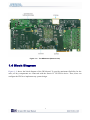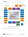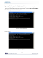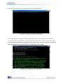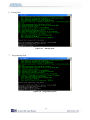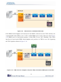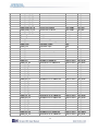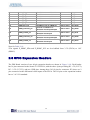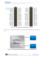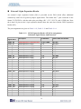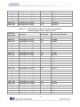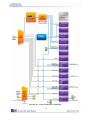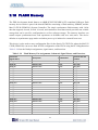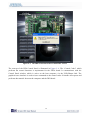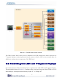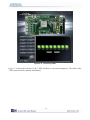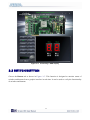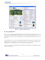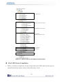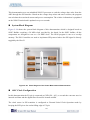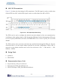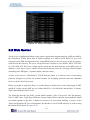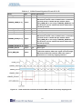
1
1 CONTENTS CHAPTER 1 OVERVIEW .......................................................................................................................................... 4 1.1 GENERAL DESCRIPTION ............................................................................................................................................ 4 1.2 KEY FEATURES.......................................................................................................................................................... 5 1.3 BOARD OVERVIEW .................................................................................................................................................... 6 1.4 BLOCK DIAGRAM ...................................................................................................................................................... 7 CHAPTER 2 USING THE DE4 BOARD ................................................................................................................ 13 2.1 CONFIGURATION OPTIONS ...................................................................................................................................... 13 2.2 SETUP ELEMENTS .................................................................................................................................................... 19 2.3 STATUS ELEMENTS .................................................................................................................................................. 20 2.4 GENERAL USER INPUT/OUTPUT .............................................................................................................................. 21 2.5 HIGH-SPEED MEZZANINE CARDS ............................................................................................................................ 25 2.6 GPIO EXPANSION HEADERS ................................................................................................................................... 36 2.7 DDR2 SO-DIMM................................................................................................................................................... 40 2.8 USB OTG............................................................................................................................................................... 48 2.9 SD CARD ................................................................................................................................................................ 51 2.10 CLOCK CIRCUITRY ................................................................................................................................................ 52 2.11 PCI EXPRESS ......................................................................................................................................................... 56 2.12 GIGABIT ETHERNET (GIGE) .................................................................................................................................. 59 2.13 SERIAL ATA (SATA) ............................................................................................................................................. 62 2.14 RS-232 SERIAL PORT ............................................................................................................................................ 64 2.15 FLASH MEMORY ................................................................................................................................................. 65 2.16 SSRAM MEMORY ................................................................................................................................................ 66 2.17 I2C SERIAL EEPROM .......................................................................................................................................... 68 2.18 TEMPERATURE SENSOR ......................................................................................................................................... 68 2.19 POWER .................................................................................................................................................................. 69 CHAPTER 3 CONTROL PANEL ............................................................................................................................ 71 3.1 CONTROL PANEL SETUP .......................................................................................................................................... 71 3.2 CONTROLLING THE LEDS AND 7-SEGMENT DISPLAYS ............................................................................................ 75 3.3 SWITCH/BUTTON ............................................................................................................................................... 77 3.4 MEMORY CONTROLLER .......................................................................................................................................... 78 3.5 USB2.0 OTG.......................................................................................................................................................... 81 2 3.6 SD CARD............................................................................................................................................................... 82 3.7 TEMPERATURE MONITOR ........................................................................................................................................ 83 3.8 POWER .................................................................................................................................................................... 84 3.9 PLL ........................................................................................................................................................................ 85 3.10 SATA.................................................................................................................................................................... 86 3.11 HSMC .................................................................................................................................................................. 87 3.12 FAN ....................................................................................................................................................................... 88 CHAPTER 4 DE4 SYSTEM BUILDER .................................................................................................................. 90 4.1 INTRODUCTION ....................................................................................................................................................... 90 4.2 GENERAL DESIGN FLOW ......................................................................................................................................... 91 4.3 USING DE4 SYSTEM BUILDER ................................................................................................................................ 92 CHAPTER 5 EXAMPLES OF ADVANCED DEMONSTRATION .................................................................... 103 5.1 USB HOST ............................................................................................................................................................ 103 5.2 USB DEVICE ......................................................................................................................................................... 111 5.3 ETHERNET – SIMPLE SOCKET SERVER ................................................................................................................... 116 5.4 SD CARD READER ................................................................................................................................................ 124 5.5 DDR2 SDRAM .................................................................................................................................................... 128 5.6 EXTERNAL CLOCK GENERATOR ............................................................................................................................ 132 5.7 POWER MEASUREMENT ........................................................................................................................................ 137 5.8 WEB SERVER......................................................................................................................................................... 141 5.9 SERIAL ATA (SATA) ............................................................................................................................................. 150 5.10 HIGH-SPEED MEZZANINE CARD (HSMC)........................................................................................................... 151 CHAPTER 6 PCI EXPRESS REFERENCE DESIGN ....................................................................................... 154 6.1 PCI EXPRESS SYSTEM INFRASTRUCTURE.............................................................................................................. 154 6.2 FPGA PCI EXPRESS SYSTEM DESIGN ................................................................................................................... 155 6.3 PC PCI EXPRESS SYSTEM DESIGN ........................................................................................................................ 159 6.4 FUNDAMENTAL COMMUNICATION ......................................................................................................................... 168 6.5 EXAMPLE 2: IMAGE PROCESS APPLICATION .......................................................................................................... 172 ADDITIONAL INFORMATION ................................................................................................................................... 177 3 Chapter 1 Overview This chapter provides an overview of the DE4 Development Board and details the components and features of the board. 1.1 General Description The DE4 Development Board provides the ideal hardware platform for system designs that demand high-performance, serial connectivity, and advanced memory interfacing. Developed specifically to address the rapidly evolving requirements in many end markets for greater bandwidth, improved jitter performance, and lower power consumption. The DE4 is powered by the Stratix® IV GX device and supported by industry-standard peripherals, connectors and interfaces that offer a rich set of features that is suitable for a wide range of compute-intensive applications. The advantages of the Stratix® IV GX FPGA platform with integrated transceivers have allowed the DE4 to fully compliant with version 2.0 of the PCI Express standard. This will accelerate mainstream development of PCI Express-based applications enabling customers to deploy designs for a broad range of high-speed connectivity applications. The DE4 coupled with serial ATA (SATA) interfaces, offer a solution for developing storage applications. The DE4 delivers fully tested and supported connectivity targeted reference design that integrates built-in blocks for PCI Express, SATA transceiver verification testing, and Gigabit Ethernet protocol. The DE4 is supported by multiple reference designs and two High-Speed Mezzanine Card (HSMC) connectors that allow scaling and customization with mezzanine daughter cards. For large-scale ASIC prototype development, it can be established by a cable connecting to multiple DE4/FPGA boards through the HSMC connectors. It is highly recommended that users read the DE4 Getting Started Guide.pdf before using the DE4 board. 4 1.2 Key Features The following hardware is implemented on the DE4 board: • Featured device o Altera Stratix® IV GX FPGA (EP4SGX230C2/EP4SGX530C2) • Configuration status and set-up elements o Built-in USB Blaster circuit for programming o Fast passive parallel (FPP) configuration via MAX II CPLD and flash memory o Three External Programmable PLL timing chip • Component and interfaces o Four Gigabit Ethernet (GigE) with RJ-45 connector o Two host and two device Serial ATA (SATA II) ports o Two HSMC connectors o Two 40-pin expansion headers o PCI Express 2.0 (x8 lane) connector • Memory o DDR2 SO-DIMM socket o FLASH o SSRAM o SD Card socket o I2C EEPROM • General user input/output: o 8 LEDs o 4 push-buttons and 4 slide switches o 8-position DIP switch o 2 seven-segment displays • Clock system o On-board clock oscillators: 50MHz and 100MHz o SMA connectors for external clock input o SMA connectors for clock output 5 • Other interfaces o USB 2.0 high-speed host/device OTG o Current sensor for FPGA current measurement o Temperature sensor 1.3 Board Over view Figure 1–1 and Figure 1–2 is the top and bottom view of the DE4 board. It depicts the layout of the board and indicates the location of the connectors and key components. Users can refer to this figure for relative location when the connectors and key components are introduced in the following chapters. Figure 1–1 The DE4 board (Top view) 6 Figure 1–2 The DE4 board (Bottom view) 1.4 Block Diagram Figure 1–3 shows the block diagram of the DE4 board. To provide maximum flexibility for the users, all key components are connected with the Stratix IV GX FPGA device. Thus, users can configure the FPGA to implement any system design. 7 Figure 1–3 Block diagram of the DE4 board Below is more detailed information regarding the blocks in Figure 1–3. 8 Stratix IV GX FPGA • EP4SGX230C2 o 228,000 logic elements (LEs) o 17,133K total memory Kbits o 1,288 18x18-bit multipliers blocks o 2 PCI Express hard IP blocks o 744 user I/Os o 8 phase locked loops (PLLs) • EP4SGX530C2 o 531,200 logic elements (LEs) o 27,376K total memory Kbits o 1,024 18x18-bit multipliers blocks o 4 PCI Express hard IP Blocks o 744 user I/Os o 8 phase locked loops (PLLs) Configuration device and USB Blaster circuit • • • • MAXII CPLD EPM2210 System Controller and Fast Passive Parallel (FPP) configuration On-board USB Blaster for use with the Quartus II Programmer Programmable PLL timing chip configured via MAX II CPLD Support JTAG mode Memory devices • • • 64MB Flash (32M x16) with a 16-bit data bus 2MB SSRAM (1M x 16) 2Kb EEPROM 9 Two DDR2 SO-DIMM sockets • • • Up to 8GB capacity in total Maximum memory clock rate at 400MHz Theortical Bandwidth over 102Gbps SD Card socket • Provides SPI and 4-bit SD mode for SD Card access General user I/O • • • 8 user controllable LEDs 2 seven-segment displays 8 user DIP switches Push-buttons • • 4 user-defined inputs Normally high; generates one active-low pulse when the switch is pressed Slide switches • • 4 slide switches for user-defined inputs When a switch is set to the DOWN or UP position, it causes logic 0 or 1, respectively. On-Board Clocking Circuitry • • • • • 50MHz/100MHz oscillator 2 SMA connector for external transceiver clock input 4 SMA connector for LVDS clock input/output 2 SMA connectors for clock output 1 SMA connector for external clock input 10 Four Serial ATA ports • SATA 3.0 standard 6Gbps signaling rate Four Gigabit Ethernet ports • Integrated 1.25GHz SERDES PCI Express x8 edge connector • • Support connection speed of Gen1 at 2.5Gbps/lane to Gen2 at 5.0Gbps/lane Connection established with PC motherboard with x8 or x16 PCI Express slot Two High Speed Mezzanine Card (HSMC) • • • • 2 female-HSMC connectors Total of 12 pairs CDR-based transceivers at data rate up to 8.5Gbps Total 38 LVDS transmitter channels at data rate up to 1.6Gbps, and 36 LVDS receiver channels I/O voltage 2.5V Two 40-pin expansion headers • 72 FPGA I/O pins, as well as 4 power and ground lines, are brought out to two 40-pin expansion connectors • • 40-pin header is designed to accept a standard 40-pin ribbon cable used for IDE hard drives Compatible with I/O standard 3.3V 11 USB Host/Slave controller • • • • • Complies fully with Universal Serial Bus Specification Rev. 2.0 Support data transfer at high-speed, full-speed, and low-speed Support both USB host and device Three USB ports (one type mini-AB for host/device and two type A for host) Support Nios II with the Terasic driver Power • • • • Standalone DC inputs 12V and 3.3V PCI Express edge connector power Optional PCI Express external power source On-Board power measurement circuitry 12 Chapter 2 Using the DE4 Board This chapter gives instructions for using the DE4 board and its components. It is strongly recommended that users read the DE4 Getting Started Guide.pdf before using the DE4 board. The document is located in the Usermanual folder on the DE4 System CD. The contents of the document include the following: • • • • • • • • Introduction to the DE4 development board DE4 development kit contents Key features Before you begin Software Installation Development board setup Programming the Stratix IV GX device on the DE4 board Programming through the Flash memory device 2.1 Configuration Options JTAG FPGA Programming over USB-Blaster The USB-blaster is implemented on the DE4 board to provide JTAG configuration through onboard USB-to-JTAG configuration logic using a type-B USB connector, a FTDI USB 2.0 Controller, and an Altera MAX II CPLD. Current configuration will be lost when the power is turned off. Figure 2–1 illustrates the JTAG configuration scheme for the DE4. 13 To download a configuration bit stream into the Stratix IV GX FPGA, perform the following steps: • • • Make sure that power is provided to the DE4 board Connect the USB cable supplied directly to the USB Blaster port of the DE4 board The FPGA can now be programmed in the Quartus II Programmer by selecting a configuration bit stream file with the .sof filename extension. Please refer to DE4 Getting Started Guide.pdf for more detailed procedure of FPGA programming. Figure 2–1 JTAG configuration scheme Flash Programming The DE4 development board contains a common flash interface (CFI) flash memory to meet the demands for a larger FPGA configuration storage. The parallel flash loader (PFL) feature in MAX II devices provides an efficient method to program CFI flash memory devices through the JTAG interface and the logic to control configuration from the flash memory device to the Stratix IV GX FPGA. Figure 2–2 depicts the connection setup between the CFI flash memory, Max II CPLD, and Stratix IV GX. 14 Please refer to the DE4 Getting Started Guide.pdf for the basic programming instruction on parallel flash loader on the CFI flash memory. Figure 2–2 Flash programming scheme Programming Flash Memory using batch file The DE4 provides a program_flash batch file (\demonstrations\de4_<Stratix device>\de4_board_ update_portal\demo_batch\Program_flash) to limit the steps that are taken when users program the flash memory on the DE4. Software Requirements: • • Quartus II 9.1 SP2 or later Nios II IDE tools 9.1 SP2 or later Program_flash folder contents: • • • • Program_flash.bat Program_flash.pl Program_flash.sh de4_board_update_portal.sof Before you use the program_flash.bat batch file to program the flash memory, make sure the DE4 is turned on and USB cable is connected to the USB blaster port (J5). In addition, place the .sof and .elf file (optional) you wish to program/convert in the Program_flash directory. 15 Programming Flash Memory with .sof using Program_flash.bat 1. Launch the program_flash.bat batch file from the directory (\demonstrations\de4_<Stratix device>\de4_board_update_portal\demo_batch\Program_flash) of the DE4 system CD-ROM. 2. The flash program tool shows the menu options. Figure 2–3 Flash program tools 3. Select option 2. Figure 2–4 Option 2 16 4. Enter the .sof file name to be programmed onto the flash memory. Figure 2–5 Enter .sof name to be program 5. The following lines will appear during flash programming: ‘Extracting Option bits SREC’, ‘Extracting FPGA Image SREC’, and ‘Deleting intermediate files’. If these lines don’t appear on the windows command, programming on the flash memory is not successfully setup. Please make sure Quartus II 9.1 SP2 and Nios II 9.1 IDE SP2 or later is used. Figure 2–6 Loading .sof file to be program 17 6. Erasing flash. Figure 2–7 Erasing flash 7. Programming flash. Figure 2–8 Programming flash 18 8. Programming complete. Figure 2–9 Programming flash complete 2.2 Setup Elements JTAG Control DIP Switch The JTAG control DIP switch is provided to either remove or include devices in the active JTAG chain. The JTAG signals (TDI and TDO) found on the HSMC connectors and PCIe interface can be enabled using a 3-position DIP switch. In the “OFF” position, the TDI and TDO signals are looped, similarly in the “ON” position, the JTAG signals are bypassed. Table 2–1 lists the position of the DIP switch and their associated interface. Table 2–1 SW8 JTAG Control DIP Switch Board Reference Signal Name SW8.1 JTAG_HSMA_EN SW8.2 JTAG_HSMB_EN SW8.3 JTAG_PCIE_EN Description On : Bypass HSMA Off: HSMA In-chain On: Bypass HSMB Off: HSMB In-chain On: Bypass PCI Express Off : PCI Express In-Chain 19 Default On On On PCI Express Control DIP switch The PCI Express Control DIP switch is provided to enable or disable different configurations of the PCIe Connector. Table 2–2 lists the switch controls and description. Table 2–2 SW9 PCIe Control DIP Switch Board Reference Signal Name Description SW9.1 PCIE_PRSNT2n_x1 SW9.2 PCIE_PRSNT2n_x4 SW9.3 PCIE_PRSNT2n_x8 On : Enable x1 presence detect Off: Disable x1 presence detect On : Enable x4 presence detect Off: Disable x4 presence detect On : Enable x8 presence detect Off: Disable x8 presence detect Default Off Off On 2.3 Status Elements The DE4 development board includes status LEDs. Please refer to Table 2–3 for the status of the LED indicator. Table 2–3 LED Indicators Board Reference LED Name Description D9 12-V Power Illuminates when 12-V power is active. D10 3.3-V Power Illuminates when 3.3-V power is active. CONF DONE Illuminates when the FPGA is successfully configured. Driven by the MAX II CPLD EPM2210 System Controller. Loading Illuminates when the MAX II CPLD EPM2210 System Controller is actively configuring the FPGA. Driven by the MAX II CPLD EPM2210 System Controller with the Embedded Blaster CPLD. D20 D18 D19 Error D12 USB Blaster Circuit Illuminates when the MAX II CPLD EPM2210 System Controller fails to configure the FPGA. Driven by the MAX II CPLD EPM2210 System Controller. Illuminates when USB blaster circuit transmits or receives data. 20 D17 HSMC Port B Present Illuminates when the HSMC port B has a board or cable plugged-in such that pin 160 becomes grounded. Driven by the add-in card D16 HSMC Port A Present Illuminates when the HSMC port A has a board or cable plugged-in such that pin 160 becomes grounded. Driven by the add-in card RXD1 UART_RXD/GPIO Illuminates when RS232 receives data or GPIO Expansion 0 Expansion 0 IO[7] IO[7] is transmits or receives. TXD1 UART_TXD/GPIO Illuminates when RS232 transmit data or GPIO Expansion 1 Expansion 1 IO[9] IO[9] is transmits or receives. USB Illuminates when USB Jack-Mini-USB port has a device. Jack-Mini-USB-AB Port USB_TYPE_A port Illuminates when the USB_TYPE_A port has a device. D15 D14 (Top USB) USB_TYPE_A port Illuminates when the USB_TYPE_A port has a device. (Bottom USB) D13 2.4 General User Input/Output Push-buttons The DE4 board includes six push-buttons that allow you to interact with the Stratix IV GX device. Each push-button provides a high logic level or a low logic level when it is not pressed or pressed, respectively. Table 2–4 lists the board references, signal names and their corresponding Stratix IV GX device pin numbers. Table 2–4 Push-button Pin Assignments, Schematic Signal Names, and Functions Board Schematic Reference Signal Name PB1 BUTTON0 PB2 PB3 PB4 PB5 PB6 Description High Logic Level when button not pressed High Logic Level when button not BUTTON1 pressed High Logic Level when button not BUTTON2 pressed High Logic Level when button not BUTTON3 pressed CPU_RESET_n FPGA reset Max II EPM2210 System RE_CONFIGn re-configuration 21 I/O Stratix IV GX Standard Pin Number 3.0-V PIN_AH5 3.0-V PIN_AG5 3.0-V PIN_AG7 3.0-V PIN_AH8 2.5-V - PIN_V34 - A CPU reset push-button (CPU_RESET_n) is an input to the Stratix IV GX device. It is intended to be the master reset signal for FPGA designs loaded into the Stratix IV GX device. The RE_CONFIGn push-button is used to force a reboot on the MAX II EPM2210 CPLD device. Slide Switches and DIP Switch There are also four slide switches and one 8-position DIP switch on the DE4 board to provide additional FPGA input control. Each switch is connected directly to a pin of the Stratix IV GX FPGA. When a slide switch is in the DOWN position or the UPPER position, it provides a low logic level or a high logic level to the FPGA, respectively. For 8-position DIP switch, when a switch is in the DOWN position or the UPPER position, it provides a high logic level or a low logic level to the FPGA. Table 2–5 and Table 2–6 lists the signal names and their corresponding Stratix IV GX device pin numbers for slide switches and DIP switch respectively. Table 2–5 Slide Switches Pin Assignments, Schematic Signal Names, and Functions Board Schematic Reference Signal Name SW0 SW1 SW2 SW3 SLIDE_SW0 SLIDE_SW1 SLIDE_SW2 SLIDE_SW3 Table 2–6 Description I/O Stratix IV GX Standard Pin Number High logic level when SW in the UPPER 2.5-V position 2.5-V 3.0-V 2.5-V PIN_J7 PIN_K7 PIN_AK6 PIN_L7 DIP Switch Pin Assignments, Schematic Signal Names, and Functions Board Schematic Reference Signal Name SW6 SW6 SW6 SW6 SW6 SW6 SW6 SW6 SW0 SW1 SW2 SW3 SW4 SW5 SW6 SW7 Description User-Defined DIP switch connected to FPGA device. When the switch is in the ON position, a logic 0 is selected. Similarly when the switch is in the OFF position, a logic 1 is selected. 22 I/O Stratix IV GX Standard Pin Number 3.0-V 3.0-V 3.0-V 3.0-V 3.0-V 3.0-V 3.0-V 3.0-V PIN_AB13 PIN_AB12 PIN_AB11 PIN_AB10 PIN_AB9 PIN_AC8 PIN_AH6 PIN_AG6 LEDs The DE4 board consists of 8 user-controllable LEDs to allow status and debugging signals to be driven to the LEDs from the designs loaded into the Stratix IV GX device. Each LED is driven directly by the Stratix IV GX FPGA. The LED is turned on or off when the associated pins are driven to a low or high logic level, respectively. A list of the pin names on the FPGA that are connected to the LEDs is given in Table 2–7. Table 2–7 Board Reference D1 D2 D3 D4 D5 D6 D7 D8 User LEDs Pin Assignments, Schematic Signal Names, and Functions Schematic Signal I/O Description Standard Pin Number Name LED0 LED1 LED2 LED3 LED4 LED5 LED6 LED7 Stratix IV GX User-Defined LEDs. Driving a logic 0 on the I/O port turns the LED ON. Driving a logic 1 on the I/O port turns the LED OFF. 2.5-V 2.5-V 2.5-V 2.5-V 2.5-V 2.5-V 2.5-V 2.5-V PIN_V28 PIN_W28 PIN_R29 PIN_P29 PIN_N29 PIN_M29 PIN_M30 PIN_N30 7-Segment Displays The DE4 board has two 7-segment displays. As indicated in the schematic in Figure 2–10, the seven segments are connected to pins of the Stratix IV GX FPGA. Applying a low or high logic level to a segment to light it up or turns it off. Each segment in a display is identified by an index listed from 0 to 6 with the positions given in Figure 2–11. In addition, the decimal point is identified as DP. Table 2–8 shows the mapping of the FPGA pin assignments to the 7-segment displays. 23 Figure 2–10 Connection between 7-segment displays and Stratix IV GX FPGA Figure 2–11 Position and index of each segment in a 7-segment display Table 2–8 Board Reference HEX1 HEX1 HEX1 HEX1 HEX1 HEX1 HEX1 HEX1 7-Segment Display Pin Assignments, Schematic Signal Names, and Functions Schematic Signal I/O Description Standard Pin Number Name SEG1_D0 SEG1_D1 SEG1_D2 SEG1_D3 SEG1_D4 SEG1_D5 SEG1_D6 SEG1_DP Stratix IV GX User-Defined 7-Segment Display. Driving a logic 0 on the I/O port turns the 7-segment signal ON. Driving a logic 1 on the I/O port turns the 7-segment signal OFF. 24 2.5-V 2.5-V 2.5-V 2.5-V 2.5-V 2.5-V 2.5-V 2.5-V PIN_E31 PIN_F31 PIN_G31 PIN_C34 PIN_C33 PIN_D33 PIN_D34 PIN_AL35 HEX0 HEX0 HEX0 HEX0 HEX0 HEX0 HEX0 HEX0 SEG0_D0 SEG0_D1 SEG0_D2 SEG0_D3 SEG0_D4 SEG0_D5 SEG0_D6 SEG0_DP 2.5-V 2.5-V 2.5-V 2.5-V 2.5-V 2.5-V 2.5-V 2.5-V PIN_L34 PIN_M34 PIN_M33 PIN_H31 PIN_J33 PIN_L35 PIN_K32 PIN_AL34 2.5 High-Speed Mezzanine Cards The DE4 development board contains two HSMC interfaces called port A and port B. The HSMC interface provides a mechanism to extend the peripheral-set of an FPGA host board by means of add-on cards, which can address today’s high speed signaling requirement as well as low-speed device interface support. The HSMC interfaces support JTAG, clock outputs and inputs, high-speed serial I/O (transceivers), and single-ended or differential signaling. Both the HSMC interfaces connected to the Stratix IV GX device are female HSMC connectors with each connector having a total of 172pins, including 121 signal pins (120 signal pins +1 PSNTn pin), 39 power pins, and 12 ground pins. The HSMC connector is based on the Samtec 0.5 mm pitch, surface-mount QSH family of high-speed, board-to-board connectors. The Stratix IV GX device provides +12 V DC and +3.3 V DC power to the mezzanine card through the HSMC connector. Table 2–9 indicates the maximum power consumption for both HSMC ports A and B. Table 2–9 Power Supply of the HSMC Supplied Voltage Max. Current Limit 12V 3A 3.3V 3A There are three banks in this connector as Figure 2–12 shows the bank arrangement of signals with respect to the Samtec connector. Table 2–10 and Table 2–11 show the mapping of the FPGA pin assignments to the HSMC connectors. 25 Figure 2–12 HSMC signal and bank diagram I/O Distribution The two HSMC interfaces combine have a total of 12 pairs CDR-based transceivers operating up to 8.5Gbps, 38 pairs LVDS transmitter channels at data rates up to 1.6Gbps, and 36 pairs LVDS receiver channels. Independently, Port A of the HSMC connector consists of 4 pairs CDR-based transceivers, 19 pairs LVDS transmitter channels, and 18 pairs LVDS receiver channels. While port B of the HSMC connector consists of 8 pairs CDR-based transceivers, 19 pairs LVDS transmitter channels, and 18 pairs LVDS receiver channels. Additionally, both ports A and B of the HSMC interfaces have 5 clock inputs and 4 clock outputs (2 differential clock inputs and outputs). I/O Standards The HSMC interface has programmable bi-directional I/O pins that can be used as 2.5-V. These pins can also be used as differential I/O standard including LVDS. Using THCB-HMF2 adapter card The purpose of the HSMC Height Extension Male to Female card (THCB-HMF2) included in the DE4 kit package is to increase the height of the HSMC connector to avoid any obstruction that 26 might take place as a HSMC daughter card is connected. The THCB-HMF2 adapter card can be connected to either ports, A or B of the HSMC connector shown in Figure 2–13. Figure 2–13 Connection setup between THCB-HMF2 adapter card and HSMC JTAG Chain on HSMC The JTAG chain on the HSMC can be activated through the 3-position DIP switch (SW8). If there is no connection established on the HSMC connectors, the 3-position DIP switch (SW8) are to set ‘On’, where the JTAG signals on the HSMC connectors are bypassed illustrated in Figure 2–14. 27 Figure 2–14 JTAG chain for a standalone DE4 board If the HSMC-based daughter card connected to the HSMC connector uses the JTAG interface, the 3-position DIP switch (SW8) is set to ‘Off’ to which HSMC port is used. In this case, from Figure 2–15 HSMC port A is used where position 1 of the SW8 is set to ‘Off’. Similarly, if the JTAG interface isn’t used on the HSMC-based daughter card, position 1 of SW8 is set to ‘On’ bypassing the JTAG signals as shown in Figure 2–16. Figure 2–15 JTAG chain for a daughter card (uses JTAG) connected to HSMC port A of the DE4 28 Figure 2–16 JTAG chain for a daughter card (JTAG not used) connected to HSMC port A of the DE4 Multi-FPGA high capacity platform through HSMC The DE4 offers a choice of two Stratix IV GX devices, EP4SGX230 and EPSGX530 which offer logic elements (LEs) up to 228,000 and 531,200, respectively to provide the flexibility for users to select a suitable device in terms of design capacity. In situations where users’ design exceeds the capacity of the FPGA, the HSMC interface can be used to connect to other FPGA system boards creating a multi-FPGA scalable system. Figure 2–17 illustrates a connection setup between two DE4 boards by connecting through port B and Port A of the HSMC connectors using a Samtec high-speed cable. Notice the JTAG switch (SW8) configuration setup where position 2 is set to ‘Off’ for port B connected on the DE4 and position 1 is set to ‘Off’ for port A connected on the DE4, allowing JTAG chain to be detected for both DE4 boards. 29 Figure 2–17 JTAG chain setup between two DE4 boards using HSMC interface Table 2–10 HSMC Port B Pin Assignments, Schematic Signal Names, and Functions HSMC Pin # Schematic Signal Name Description I/O Standard 1 2 3 4 5 6 7 8 9 10 11 12 13 14 15 16 17 18 19 20 21 22 23 24 25 Transceiver TX bit 7 Transceiver RX bit 7 Transceiver TX bit 7n Transceiver RX bit 7n Transceiver TX bit 6 Transceiver RX bit 6 Transceiver TX bit 6n Transceiver RX bit 6n Transceiver TX bit 5 Transceiver RX bit 5 Transceiver RX bit 5n Transceiver RX bit 5n Transceiver TX bit 4 Transceiver RX bit 4 Transceiver TX bit 4n Transceiver RX bit 4n Transceiver TX bit 3 Transceiver RX bit 3 Transceiver TX bit 3n Transceiver RX bit 3n Transceiver TX bit 2 Transceiver RX bit 2 Transceiver TX bit 2n Transceiver RX bit 2n Transceiver TX bit 1 1.4-V PCML 1.4-V PCML 1.4-V PCML 1.4-V PCML 1.4-V PCML 1.4-V PCML 1.4-V PCML 1.4-V PCML 1.4-V PCML 1.4-V PCML 1.4-V PCML 1.4-V PCML 1.4-V PCML 1.4-V PCML 1.4-V PCML 1.4-V PCML 1.4-V PCML 1.4-V PCML 1.4-V PCML 1.4-V PCML 1.4-V PCML 1.4-V PCML 1.4-V PCML 1.4-V PCML 1.4-V PCML HSMB_GXB_TX_p7 HSMB_GXB_RX_p7 HSMB_GXB_TX_n7 HSMB_GXB_RX_n7 HSMB_GXB_TX_p6 HSMB_GXB_RX_p6 HSMB_GXB_TX_n6 HSMB_GXB_RX_n6 HSMB_GXB_TX_p5 HSMB_GXB_RX_p5 HSMB_GXB_TX_n5 HSMB_GXB_RX_n5 HSMB_GXB_TX_p4 HSMB_GXB_RX_p4 HSMB_GXB_TX_n4 HSMB_GXB_RX_n4 HSMB_GXB_TX_p3 HSMB_GXB_RX_p3 HSMB_GXB_TX_n3 HSMB_GXB_RX_n3 HSMB_GXB_TX_p2 HSMB_GXB_RX_p2 HSMB_GXB_TX_n2 HSMB_GXB_RX_n2 HSMB_GXB_TX_p1 30 Stratix IV GX Pin Number PIN_B4 PIN_C2 PIN_B3 PIN_C1 PIN_D4 PIN_E2 PIN_D3 PIN_E1 PIN_K4 PIN_L2 PIN_K3 PIN_L1 PIN_M4 PIN_N2 PIN_M3 PIN_N1 PIN_P4 PIN_R2 PIN_P3 PIN_R1 PIN_T4 PIN_U2 PIN_T3 PIN_U1 PIN_AB4 26 27 28 29 30 31 32 33 34 35 36 37 38 39 40 41 42 43 44 47 48 49 50 53 54 55 56 59 60 61 62 65 66 67 68 71 72 73 74 77 78 79 80 83 HSMB_GXB_RX_p1 HSMB_GXB_TX_n1 HSMB_GXB_RX_n1 HSMB_GXB_TX_p0 HSMB_GXB_RX_p0 HSMB_GXB_TX_n0 HSMB_GXB_RX_n0 E_HSMC_SDA E_HSMC_SCL HSMC_TCK HSMC_TMS HSMB_TDO HSMC_TDI HSMB_OUT0 HSMB_CLKIN0 HSMB_D0 HSMB_D1 HSMB_D2 HSMB_D3 HSMB_TX_p0 HSMB_RX_p0 HSMB_TX_n0 HSMB_RX_n0 HSMB_TX_p1 HSMB_RX_p1 HSMB_TX_n1 HSMB_RX_n1 HSMB_TX_p2 HSMB_RX_p2 HSMB_TX_n2 HSMB_RX_n2 HSMB_TX_p3 HSMB_RX_p3 HSMB_TX_n3 HSMB_RX_n3 HSMB_TX_p4 HSMB_RX_p4 HSMB_TX_n4 HSMB_RX_n4 HSMB_TX_p5 HSMB_RX_p5 HSMB_TX_n5 HSMB_RX_n5 HSMB_TX_p6 Transceiver RX bit 1 Transceiver TX bit 1n Transceiver RX bit 1n Transceiver TX bit 0 Transceiver RX bit 0 Transceiver TX bit 0n Transceiver RX bit 0n Management serial data Management serial clock JTAG clock signal JTAG mode select signal JTAG data output JTAG data input CMOS I/O Dedicated clock input LVDS TX or CMOS I/O LVDS RX or CMOS I/O LVDS TX or CMOS I/O LVDS RX or CMOS I/O LVDS TX bit 0 or CMOS I/O LVDS RX bit 0 or CMOS I/O LVDS TX bit 0n or CMOS I/O LVDS RX bit 0n or CMOS I/O LVDS TX bit 1 or CMOS I/O LVDS RX bit 1 or CMOS I/O LVDS TX bit 1n or CMOS I/O LVDS RX bit 1n or CMOS I/O LVDS TX bit 2 or CMOS I/O LVDS RX bit 2 or CMOS I/O LVDS TX bit 2n or CMOS I/O LVDS RX bit 2n or CMOS I/O LVDS TX bit 3 or CMOS I/O LVDS RX bit 3 or CMOS I/O LVDS TX bit 3n or CMOS I/O LVDS RX bit 3n or CMOS I/O LVDS TX bit 4 or CMOS I/O LVDS RX bit 4 or CMOS I/O LVDS TX bit 4n or CMOS I/O LVDS RX bit 4n or CMOS I/O LVDS TX bit 5 or CMOS I/O LVDS RX bit 5 or CMOS I/O LVDS TX bit 5n or CMOS I/O LVDS RX bit 5n or CMOS I/O LVDS TX bit 6 or CMOS I/O 31 1.4-V PCML 1.4-V PCML 1.4-V PCML 1.4-V PCML 1.4-V PCML 1.4-V PCML 1.4-V PCML 1.8-V(*) 1.8-V(*) 2.5-V 2.5-V 2.5-V 2.5-V LVDS or 2.5-V LVDS or 2.5-V LVDS or 2.5-V LVDS or 2.5-V LVDS or 2.5-V LVDS or 2.5-V LVDS or 2.5-V LVDS or 2.5-V LVDS or 2.5-V LVDS or 2.5-V LVDS or 2.5-V LVDS or 2.5-V LVDS or 2.5-V LVDS or 2.5-V LVDS or 2.5-V LVDS or 2.5-V LVDS or 2.5-V LVDS or 2.5-V LVDS or 2.5-V LVDS or 2.5-V LVDS or 2.5-V LVDS or 2.5-V LVDS or 2.5-V LVDS or 2.5-V LVDS or 2.5-V LVDS or 2.5-V LVDS or 2.5-V LVDS or 2.5-V LVDS or 2.5-V LVDS or 2.5-V LVDS or 2.5-V PIN_AC2 PIN_AB3 PIN_AC1 PIN_AD4 PIN_AE2 PIN_AD3 PIN_AE1 PIN_M19 PIN_L19 PIN_L8 PIN_AA5 PIN_H10 PIN_D6 PIN_G10 PIN_C6 PIN_K9 PIN_D5 PIN_J9 PIN_C5 PIN_K10 PIN_D10 PIN_J10 PIN_C10 PIN_N11 PIN_D9 PIN_N10 PIN_C9 PIN_N12 PIN_D8 PIN_M12 PIN_C8 PIN_R12 PIN_D7 PIN_R11 PIN_C7 PIN_T13 PIN_F10 PIN_T12 PIN_E10 PIN_R13 84 85 86 89 90 91 92 95 HSMB_RX_p6 HSMB_TX_n6 HSMB_RX_n6 HSMB_TX_p7 HSMB_RX_p7 HSMB_TX_n7 HSMB_RX_n7 HSMB_OUT_p1 96 HSMB_CLKIN_p1 97 HSMB_OUT_n1 98 HSMB_CLKIN_n1 101 102 103 104 107 108 109 110 113 114 115 116 119 120 121 122 125 126 127 128 131 132 133 134 137 138 139 140 143 144 145 HSMB_TX_p8 HSMB_RX_p8 HSMB_TX_n8 HSMB_RX_n8 HSMB_TX_p9 HSMB_RX_p9 HSMB_TX_n9 HSMB_RX_n9 HSMB_TX_p10 HSMB_RX_p10 HSMB_TX_n10 HSMB_RX_n10 HSMB_TX_p11 HSMB_RX_p11 HSMB_TX_n11 HSMB_RX_n11 HSMB_TX_p12 HSMB_RX_p12 HSMB_TX_n12 HSMB_RX_n12 HSMB_TX_p13 HSMB_RX_p13 HSMB_TX_n13 HSMB_RX_n13 HSMB_TX_p14 HSMB_RX_p14 HSMB_TX_n14 HSMB_RX_n14 HSMB_TX_p15 HSMB_RX_p15 HSMB_TX_n15 LVDS RX bit 6 or CMOS I/O LVDS TX bit 6n or CMOS I/O LVDS RX bit 6n or CMOS I/O LVDS TX bit 7 or CMOS I/O LVDS RX bit 7 or CMOS I/O LVDS TX bit 7n or CMOS I/O LVDS RX bit 7n or CMOS I/O LVDS TX or CMOS I/O LVDS RX or CMOS I/O or differential clock input LVDS RX or CMOS I/O LVDS RX or CMOS I/O or differential clock input LVDS TX bit 8 or CMOS I/O LVDS RX bit 8 or CMOS I/O LVDS TX bit 8n or CMOS I/O LVDS RX bit 8n or CMOS I/O LVDS TX bit 9 or CMOS I/O LVDS RX bit 9 or CMOS I/O LVDS TX bit 9n or CMOS I/O LVDS RX bit 9n or CMOS I/O LVDS TX bit 10 or CMOS I/O LVDS RX bit 10 or CMOS I/O LVDS TX bit 10n or CMOS I/O LVDS RX bit 10n or CMOS I/O LVDS TX bit 11 or CMOS I/O LVDS RX bit 11 or CMOS I/O LVDS TX bit 11n or CMOS I/O LVDS RX bit 11n or CMOS I/O LVDS TX bit 12 or CMOS I/O LVDS RX bit 12 or CMOS I/O LVDS TX bit 12n or CMOS I/O LVDS RX bit 12n or CMOS I/O LVDS TX bit 13 or CMOS I/O LVDS RX bit 13 or CMOS I/O LVDS TX bit 13n or CMOS I/O LVDS RX bit 13n or CMOS I/O LVDS TX bit 14 or CMOS I/O LVDS RX bit 14 or CMOS I/O LVDS TX bit 14n or CMOS I/O LVDS RX bit 14n or CMOS I/O LVDS TX bit 15 or CMOS I/O LVDS RX bit 15 or CMOS I/O LVDS TX bit 15n or CMOS I/O 32 LVDS or 2.5-V LVDS or 2.5-V LVDS or 2.5-V LVDS or 2.5-V LVDS or 2.5-V LVDS or 2.5-V LVDS or 2.5-V LVDS or 2.5-V PIN_G5 PIN_P13 PIN_F5 PIN_H7 PIN_G6 PIN_G7 PIN_F6 PIN_K8 LVDS or 2.5-V PIN_W34 LVDS or 2.5-V PIN_J8 LVDS or 2.5-V PIN_W35 LVDS or 2.5-V LVDS or 2.5-V LVDS or 2.5-V LVDS or 2.5-V LVDS or 2.5-V LVDS or 2.5-V LVDS or 2.5-V LVDS or 2.5-V LVDS or 2.5-V LVDS or 2.5-V LVDS or 2.5-V LVDS or 2.5-V LVDS or 2.5-V LVDS or 2.5-V LVDS or 2.5-V LVDS or 2.5-V LVDS or 2.5-V LVDS or 2.5-V LVDS or 2.5-V LVDS or 2.5-V LVDS or 2.5-V LVDS or 2.5-V LVDS or 2.5-V LVDS or 2.5-V LVDS or 2.5-V LVDS or 2.5-V LVDS or 2.5-V LVDS or 2.5-V LVDS or 2.5-V LVDS or 2.5-V LVDS or 2.5-V PIN_M10 PIN_F7 PIN_L10 PIN_E7 PIN_M8 PIN_G8 PIN_M7 PIN_F8 PIN_M11 PIN_G9 PIN_L11 PIN_F9 PIN_N9 PIN_N6 PIN_P8 PIN_N5 PIN_R9 PIN_M6 PIN_R8 PIN_L5 PIN_U10 PIN_R6 PIN_T9 PIN_R5 PIN_V10 PIN_R7 PIN_V9 PIN_P6 PIN_T10 PIN_V6 PIN_R10 146 149 150 151 152 HSMB_RX_n15 HSMB_TX_p16 HSMB_RX_p16 HSMB_TX_n16 HSMB_RX_n16 155 HSMB_CLKOUT_p2 156 HSMB_CLKIN_p2 157 HSMB_CLKOUT_n2 158 HSMB_CLKIN_n2 LVDS RX bit 15n or CMOS I/O LVDS TX bit 16 or CMOS I/O LVDS RX bit 16 or CMOS I/O LVDS TX bit 16n or CMOS I/O LVDS RX bit 16n or CMOS I/O LVDS TX or CMOS I/O or differential clock input/output LVDS RX or CMOS I/O or differential clock input LVDS TX or CMOS I/O or differential clock input/output LVDS RX or CMOS I/O or differential clock input LVDS or 2.5-V LVDS or 2.5-V LVDS or 2.5-V LVDS or 2.5-V LVDS or 2.5-V PIN_U5 PIN_V12 PIN_W8 PIN_V11 PIN_W7 LVDS or 2.5-V PIN_W12 LVDS or 2.5-V PIN_W6 LVDS or 2.5-V PIN_W11 LVDS or 2.5-V PIN_W5 Note for Table 2–10: *The signals E_HSMC_SDA and E_HSMC_SCL are level-shifted from 3.3V (FPGA) to 1.8V (HSMC). Table 2–11 HSMC Port A Pin Assignments, Schematic Signal Names, and Functions HSMC Pin # Schematic Signal Name Description I/O Standard 1 2 3 4 5 6 7 8 9 10 11 12 13 14 15 16 17 18 19 20 21 22 23 1.4-V PCML 1.4-V PCML 1.4-V PCML 1.4-V PCML 1.4-V PCML 1.4-V PCML 1.4-V PCML HSMA_GXB_TX_p3 HSMA_GXB_RX_p3 HSMA_GXB_TX_n3 HSMA_GXB_RX_n3 HSMA_GXB_TX_p2 HSMA_GXB_RX_p2 HSMA_GXB_TX_n2 Transceiver TX bit 3 Transceiver RX bit 3 Transceiver TX bit 3n Transceiver RX bit 3n Transceiver TX bit 2 Transceiver RX bit 2 Transceiver TX bit 2n 33 Stratix IV GX Pin Number PIN_B36 PIN_C38 PIN_B37 PIN_C39 PIN_D36 PIN_E38 PIN_D37 24 25 26 27 28 29 30 31 32 33 34 35 36 37 38 39 40 41 42 43 44 47 48 49 50 53 54 55 56 59 60 61 62 65 66 67 68 71 72 73 74 77 78 79 HSMA_GXB_RX_n2 HSMA_GXB_TX_p1 HSMA_GXB_RX_p1 HSMA_GXB_TX_n1 HSMA_GXB_RX_n1 HSMA_GXB_TX_p0 HSMA_GXB_RX_p0 HSMA_GXB_TX_n0 HSMA_GXB_RX_n0 E_HSMC_SDA E_HSMC_SCL HSMC_TCK HSMC_TMS HSMA_TDO HSMA_TDI HSMA_OUT0 HSMA_CLKIN0 HSMA_D0 HSMA_D1 HSMA_D2 HSMA_D3 HSMA_TX_p0 HSMA_RX_p0 HSMA_TX_n0 HSMA_RX_n0 HSMA_TX_p1 HSMA_RX_p1 HSMA_TX_n1 HSMA_RX_n1 HSMA_TX_p2 HSMA_RX_p2 HSMA_TX_n2 HSMA_RX_n2 HSMA_TX_p3 HSMA_RX_p3 HSMA_TX_n3 HSMA_RX_n3 HSMA_TX_p4 HSMA_RX_p4 HSMA_TX_n4 HSMA_RX_n4 HSMA_TX_p5 HSMA_RX_p5 HSMA_TX_n5 Transceiver RX bit 2n Transceiver TX bit 1 Transceiver RX bit 1 Transceiver TX bit 1n Transceiver RX bit 1n Transceiver TX bit 0 Transceiver RX bit 0 Transceiver TX bit 0n Transceiver RX bit 0n Management serial data Management serial clock JTAG clock signal JTAG mode select signal JTAG data output JTAG data input CMOS I/O Dedicated clock input LVDS TX or CMOS I/O LVDS RX or CMOS I/O LVDS TX or CMOS I/O LVDS RX or CMOS I/O LVDS TX bit 0 or CMOS I/O LVDS RX bit 0 or CMOS I/O LVDS TX bit 0n or CMOS I/O LVDS RX bit 0n or CMOS I/O LVDS TX bit 1 or CMOS I/O LVDS RX bit 1 or CMOS I/O LVDS TX bit 1n or CMOS I/O LVDS RX bit 1n or CMOS I/O LVDS TX bit 2 or CMOS I/O LVDS RX bit 2 or CMOS I/O LVDS TX bit 2n or CMOS I/O LVDS RX bit 2n or CMOS I/O LVDS TX bit 3 or CMOS I/O LVDS RX bit 3 or CMOS I/O LVDS TX bit 3n or CMOS I/O LVDS RX bit 3n or CMOS I/O LVDS TX bit 4 or CMOS I/O LVDS RX bit 4 or CMOS I/O LVDS TX bit 4n or CMOS I/O LVDS RX bit 4n or CMOS I/O LVDS TX bit 5 or CMOS I/O LVDS RX bit 5 or CMOS I/O LVDS TX bit 5n or CMOS I/O 34 1.4-V PCML 1.4-V PCML 1.4-V PCML 1.4-V PCML 1.4-V PCML 1.4-V PCML 1.4-V PCML 1.4-V PCML 1.4-V PCML 1.8-V(*) 1.8-V(*) 2.5-V 2.5-V 2.5-V 2.5-V LVDS or 2.5-V LVDS or 2.5-V LVDS or 2.5-V LVDS or 2.5-V LVDS or 2.5-V LVDS or 2.5-V LVDS or 2.5-V LVDS or 2.5-V LVDS or 2.5-V LVDS or 2.5-V LVDS or 2.5-V LVDS or 2.5-V LVDS or 2.5-V LVDS or 2.5-V LVDS or 2.5-V LVDS or 2.5-V LVDS or 2.5-V LVDS or 2.5-V LVDS or 2.5-V LVDS or 2.5-V LVDS or 2.5-V LVDS or 2.5-V LVDS or 2.5-V LVDS or 2.5-V LVDS or 2.5-V LVDS or 2.5-V LVDS or 2.5-V LVDS or 2.5-V LVDS or 2.5-V PIN_E39 PIN_K36 PIN_L38 PIN_K37 PIN_L39 PIN_M36 PIN_N38 PIN_M37 PIN_N39 PIN_M19 PIN_L19 PIN_AF29 PIN_AC34 PIN_AC26 PIN_AC31 PIN_AD26 PIN_AC32 PIN_AB27 PIN_AJ32 PIN_AB28 PIN_AK33 PIN_AB30 PIN_AH34 PIN_AB31 PIN_AH35 PIN_AD27 PIN_AJ34 PIN_AE27 PIN_AJ35 PIN_AD28 PIN_AK34 PIN_AD29 PIN_AK35 PIN_AE28 PIN_AN30 PIN_AE29 PIN_AP30 PIN_AE26 PIN_AM34 PIN_AF26 80 83 84 85 86 89 90 91 92 95 HSMA_RX_n5 HSMA_TX_p6 HSMA_RX_p6 HSMA_TX_n6 HSMA_RX_n6 HSMA_TX_p7 HSMA_RX_p7 HSMA_TX_n7 HSMA_RX_n7 HSMA_OUT_p1 96 HSMA_CLKIN_p1 97 HSMA_OUT_n1 98 HSMA_CLKIN_n1 101 102 103 104 107 108 109 110 113 114 115 116 119 120 121 122 125 126 127 128 131 132 133 134 137 138 139 140 143 HSMA_TX_p8 HSMA_RX_p8 HSMA_TX_n8 HSMA_RX_n8 HSMA_TX_p9 HSMA_RX_p9 HSMA_TX_n9 HSMA_RX_n9 HSMA_TX_p10 HSMA_RX_p10 HSMA_TX_n10 HSMA_RX_n10 HSMA_TX_p11 HSMA_RX_p11 HSMA_TX_n11 HSMA_RX_n11 HSMA_TX_p12 HSMA_RX_p12 HSMA_TX_n12 HSMA_RX_n12 HSMA_TX_p13 HSMA_RX_p13 HSMA_TX_n13 HSMA_RX_n13 HSMA_TX_p14 HSMA_RX_p14 HSMA_TX_n14 HSMA_RX_n14 HSMA_TX_p15 LVDS RX bit 5n or CMOS I/O LVDS TX bit 6 or CMOS I/O LVDS RX bit 6 or CMOS I/O LVDS TX bit 6n or CMOS I/O LVDS RX bit 6n or CMOS I/O LVDS TX bit 7 or CMOS I/O LVDS RX bit 7 or CMOS I/O LVDS TX bit 7n or CMOS I/O LVDS RX bit 7n or CMOS I/O LVDS TX or CMOS I/O LVDS RX or CMOS I/O or differential clock input LVDS RX or CMOS I/O LVDS RX or CMOS I/O or differential clock input LVDS TX bit 8 or CMOS I/O LVDS RX bit 8 or CMOS I/O LVDS TX bit 8n or CMOS I/O LVDS RX bit 8n or CMOS I/O LVDS TX bit 9 or CMOS I/O LVDS RX bit 9 or CMOS I/O LVDS TX bit 9n or CMOS I/O LVDS RX bit 9n or CMOS I/O LVDS TX bit 10 or CMOS I/O LVDS RX bit 10 or CMOS I/O LVDS TX bit 10n or CMOS I/O LVDS RX bit 10n or CMOS I/O LVDS TX bit 11 or CMOS I/O LVDS RX bit 11 or CMOS I/O LVDS TX bit 11n or CMOS I/O LVDS RX bit 11n or CMOS I/O LVDS TX bit 12 or CMOS I/O LVDS RX bit 12 or CMOS I/O LVDS TX bit 12n or CMOS I/O LVDS RX bit 12n or CMOS I/O LVDS TX bit 13 or CMOS I/O LVDS RX bit 13 or CMOS I/O LVDS TX bit 13n or CMOS I/O LVDS RX bit 13n or CMOS I/O LVDS TX bit 14 or CMOS I/O LVDS RX bit 14 or CMOS I/O LVDS TX bit 14n or CMOS I/O LVDS RX bit 14n or CMOS I/O LVDS TX bit 15 or CMOS I/O 35 LVDS or 2.5-V LVDS or 2.5-V LVDS or 2.5-V LVDS or 2.5-V LVDS or 2.5-V LVDS or 2.5-V LVDS or 2.5-V LVDS or 2.5-V LVDS or 2.5-V LVDS or 2.5-V PIN_AM35 PIN_AG31 PIN_AM31 PIN_AG32 PIN_AN31 PIN_AG29 PIN_AN33 PIN_AH29 PIN_AP34 PIN_AG28 LVDS or 2.5-V PIN_AB34 LVDS or 2.5-V PIN_AH28 LVDS or 2.5-V PIN_AA35 LVDS or 2.5-V LVDS or 2.5-V LVDS or 2.5-V LVDS or 2.5-V LVDS or 2.5-V LVDS or 2.5-V LVDS or 2.5-V LVDS or 2.5-V LVDS or 2.5-V LVDS or 2.5-V LVDS or 2.5-V LVDS or 2.5-V LVDS or 2.5-V LVDS or 2.5-V LVDS or 2.5-V LVDS or 2.5-V LVDS or 2.5-V LVDS or 2.5-V LVDS or 2.5-V LVDS or 2.5-V LVDS or 2.5-V LVDS or 2.5-V LVDS or 2.5-V LVDS or 2.5-V LVDS or 2.5-V LVDS or 2.5-V LVDS or 2.5-V LVDS or 2.5-V LVDS or 2.5-V PIN_AC28 PIN_AP32 PIN_AC29 PIN_AR32 PIN_AJ29 PIN_AR31 PIN_AK29 PIN_AT30 PIN_AD30 PIN_AT33 PIN_AD31 PIN_AU33 PIN_AK32 PIN_AU34 PIN_AL32 PIN_AV34 PIN_AG27 PIN_AT32 PIN_AH27 PIN_AU32 PIN_AK31 PIN_AT31 PIN_AL31 PIN_AU31 PIN_AJ31 PIN_AP35 PIN_AH30 PIN_AR35 PIN_AL29 144 145 146 149 150 151 152 HSMA_RX_p15 HSMA_TX_n15 HSMA_RX_n15 HSMA_TX_p16 HSMA_RX_p16 HSMA_TX_n16 HSMA_RX_n16 155 HSMA_CLKOUT_p2 156 HSMA_CLKIN_p2 157 HSMA_CLKOUT_n2 158 HSMA_CLKIN_n2 LVDS RX bit 15 or CMOS I/O LVDS TX bit 15n or CMOS I/O LVDS RX bit 15n or CMOS I/O LVDS TX bit 16 or CMOS I/O LVDS RX bit 16 or CMOS I/O LVDS TX bit 16n or CMOS I/O LVDS RX bit 16n or CMOS I/O LVDS TX or CMOS I/O or differential clock input/output LVDS RX or CMOS I/O or differential clock input LVDS TX or CMOS I/O or differential clock input/output LVDS RX or CMOS I/O or differential clock input LVDS or 2.5-V LVDS or 2.5-V LVDS or 2.5-V LVDS or 2.5-V LVDS or 2.5-V LVDS or 2.5-V LVDS or 2.5-V PIN_AN32 PIN_AM29 PIN_AP33 PIN_AK30 PIN_AT34 PIN_AL30 PIN_AR34 LVDS or 2.5-V PIN_AG34 LVDS or 2.5-V PIN_AF34 LVDS or 2.5-V PIN_AG35 LVDS or 2.5-V PIN_AE35 Note for Table 2–11: *The signals E_HSMC_SDA and E_HSMC_SCL are level-shifted from 3.3V (FPGA) to 1.8V (HSMC). 2.6 GPIO Expansion Headers The DE4 Board consists of two 40-pin expansion headers as shown in Figure 2–18. Each header has 36 pins connected to the Stratix IV GX FPGA, with the other 4 pins providing DC +5V (VCC5), DC +3.3V (VCC33), and two GND pins. Among these 36 I/O pins for connector JP3, there are 2 pins connected to the differential clock inputs of the FPGA. The I/O pins on the expansion headers have a 3.0-V I/O standard. 36 Figure 2–18 Pin distribution of the GPIO expansion headers Finally, Figure 2–19 shows the connections between the GPIO expansion headers and Stratix IV GX. Figure 2–19 Connection between the GPIO expansion headers and Stratix IV GX 37 External 14-pin Expansion Header An external 14-pin expansion header (JP6) is provided on the DE4 which offers additional connectivity and I/Os for general purpose applications. The header has 7 pins connected to the Stratix IV GX FPGA, with the other pins providing a DC +3.3V (VCC33) and 6 GND pins. Note the 6 data I/O pins on the 14-pin expansion header share the same bus with the GPIO expansion header (JP3). The pin assignments are given in Table 2–12, Table 2–13 and Table 2–14. Table 2–12 GPIO Expansion Header (JP3) Pin Assignments, Schematic Signal Names, and Functions Schematic Signal Name GPIO0_D0 GPIO0_D1 GPIO0_D2 GPIO0_D3 GPIO0_D4 GPIO0_D5 GPIO0_D6 GPIO0_D7 GPIO0_D8 GPIO0_D9 GPIO0_D10 GPIO0_D11 GPIO0_D12 GPIO0_D13 GPIO0_D14 GPIO0_D15 GPIO0_D16 GPIO0_D17 GPIO0_D18 GPIO0_D19 GPIO0_D20 GPIO0_D21 GPIO0_D22 GPIO0_D23 GPIO0_D24 GPIO0_D25 GPIO0_D26 GPIO0_D27 Description I/O Standard Stratix IV GX Pin Number GPIO Expansion 0 IO[0](Clock In) GPIO Expansion 0 IO[1] GPIO Expansion 0 IO[2](Clock In) GPIO Expansion 0 IO[3] GPIO Expansion 0 IO[4] GPIO Expansion 0 IO[5] GPIO Expansion 0 IO[6] GPIO Expansion 0 IO[7] GPIO Expansion 0 IO[8] GPIO Expansion 0 IO[9] GPIO Expansion 0 IO[10] GPIO Expansion 0 IO[11] GPIO Expansion 0 IO[12] GPIO Expansion 0 IO[13] GPIO Expansion 0 IO[14] GPIO Expansion 0 IO[15] GPIO Expansion 0 IO[16] GPIO Expansion 0 IO[17] GPIO Expansion 0 IO[18] GPIO Expansion 0 IO[19] GPIO Expansion 0 IO[20] GPIO Expansion 0 IO[21] GPIO Expansion 0 IO[22] GPIO Expansion 0 IO[23] GPIO Expansion 0 IO[24] GPIO Expansion 0 IO[25] GPIO Expansion 0 IO[26] GPIO Expansion 0 IO[27] 3.0-V or LVDS 3.0-V 3.0-V or LVDS 3.0-V 3.0-V 3.0-V 3.0-V 3.0-V 3.0-V 3.0-V 3.0-V 3.0-V 3.0-V 3.0-V 3.0-V 3.0-V 3.0-V 3.0-V 3.0-V 3.0-V 3.0-V 3.0-V 3.0-V 3.0-V 3.0-V 3.0-V 3.0-V 3.0-V PIN_AF6 PIN_AU9 PIN_AE5 PIN_AR8 PIN_AN9 PIN_AP9 PIN_AV5 PIN_AW6 PIN_AV7 PIN_AW7 PIN_AT5 PIN_AT8 PIN_AP5 PIN_AP7 PIN_AN5 PIN_AN10 PIN_AM5 PIN_AM10 PIN_AL10 PIN_AM8 PIN_AL8 PIN_AK8 PIN_AJ11 PIN_AK7 PIN_AJ5 PIN_AH12 PIN_AG10 PIN_AG13 38 GPIO0_D28 GPIO0_D29 GPIO0_D30 GPIO0_D31 GPIO0_D32 GPIO0_D33 GPIO0_D34 GPIO0_D35 GPIO Expansion 0 IO[28] GPIO Expansion 0 IO[29] GPIO Expansion 0 IO[30] GPIO Expansion 0 IO[31] GPIO Expansion 0 IO[32] GPIO Expansion 0 IO[33] GPIO Expansion 0 IO[34] GPIO Expansion 0 IO[35] Table 2–13 Schematic Signal Name GPIO1_D0 GPIO1_D1 GPIO1_D2 GPIO1_D3 GPIO1_D4 GPIO1_D5 GPIO1_D6 GPIO1_D7 GPIO1_D8 GPIO1_D9 GPIO1_D10 GPIO1_D11 GPIO1_D12 GPIO1_D13 GPIO1_D14 GPIO1_D15 GPIO1_D16 GPIO1_D17 GPIO1_D18 GPIO1_D19 GPIO1_D20 GPIO1_D21 GPIO1_D22 GPIO1_D23 GPIO1_D24 GPIO1_D25 GPIO1_D26 GPIO1_D27 GPIO1_D28 GPIO1_D29 3.0-V 3.0-V 3.0-V 3.0-V 3.0-V 3.0-V 3.0-V 3.0-V PIN_AG9 PIN_AF11 PIN_AT9 PIN_AF10 PIN_AD10 PIN_AP10 PIN_AD12 PIN_AD13 GPIO Expansion Header (JP4) Pin Assignments, Schematic Signal Names, and Functions Description I/O Standard Stratix IV GX Pin Number GPIO Expansion 1 IO[0] GPIO Expansion 1 IO[1] GPIO Expansion 1 IO[2] GPIO Expansion 1 IO[3] GPIO Expansion 1 IO[4] GPIO Expansion 1 IO[5] GPIO Expansion 1 IO[6] GPIO Expansion 1 IO[7] GPIO Expansion 1 IO[8] GPIO Expansion 1 IO[9] GPIO Expansion 1 IO[10] GPIO Expansion 1 IO[11] GPIO Expansion 1 IO[12] GPIO Expansion 1 IO[13] GPIO Expansion 1 IO[14] GPIO Expansion 1 IO[15] GPIO Expansion 1 IO[16] GPIO Expansion 1 IO[17] GPIO Expansion 1 IO[18] GPIO Expansion 1 IO[19] GPIO Expansion 1 IO[20] GPIO Expansion 1 IO[21] GPIO Expansion 1 IO[22] GPIO Expansion 1 IO[23] GPIO Expansion 1 IO[24] GPIO Expansion 1 IO[25] GPIO Expansion 1 IO[26] GPIO Expansion 1 IO[27] GPIO Expansion 1 IO[28] GPIO Expansion 1 IO[29] 3.0-V 3.0-V 3.0-V 3.0-V 3.0-V 3.0-V 3.0-V 3.0-V 3.0-V 3.0-V 3.0-V 3.0-V 3.0-V 3.0-V 3.0-V 3.0-V 3.0-V 3.0-V 3.0-V 3.0-V 3.0-V 3.0-V 3.0-V 3.0-V 3.0-V 3.0-V 3.0-V 3.0-V 3.0-V 3.0-V PIN_AW5 PIN_AW8 PIN_AW4 PIN_AV10 PIN_AV8 PIN_AW10 PIN_AU10 PIN_AU8 PIN_AP8 PIN_AT10 PIN_AU6 PIN_AT6 PIN_AU7 PIN_AR5 PIN_AP6 PIN_AT7 PIN_AN7 PIN_AN6 PIN_AL6 PIN_AM6 PIN_AL5 PIN_AL9 PIN_AK9 PIN_AJ6 PIN_AJ10 PIN_AH11 PIN_AH8 PIN_AH9 PIN_AG12 PIN_AH10 39 GPIO1_D30 GPIO1_D31 GPIO1_D32 GPIO1_D33 GPIO1_D34 GPIO1_D35 GPIO Expansion 1 IO[30] GPIO Expansion 1 IO[31] GPIO Expansion 1 IO[32] GPIO Expansion 1 IO[33] GPIO Expansion 1 IO[34] GPIO Expansion 1 IO[35] Table 2–14 Schematic Signal Name GPIO0_D0 GPIO0_D1 GPIO0_D2 GPIO0_D3 GPIO0_D4 GPIO0_D5 GPIO0_D6 3.0-V 3.0-V 3.0-V 3.0-V 3.0-V 3.0-V PIN_AF13 PIN_AE13 PIN_AE10 PIN_AP10 PIN_AE12 PIN_AE11 External 14-pin Expansion Header (JP6) Pin Assignments, Schematic Signal Names, and Functions Description I/O Standard Stratix IV GX Pin Number GPIO Expansion 0 IO[0](Clock In) GPIO Expansion 0 IO[1] GPIO Expansion 0 IO[2](Clock In) GPIO Expansion 0 IO[3] GPIO Expansion 0 IO[4] GPIO Expansion 0 IO[5] GPIO Expansion 0 IO[6] 3.0-V or LVDS 3.0-V 3.0-V or LVDS 3.0-V 3.0-V 3.0-V 3.0-V PIN_AF6 PIN_AU9 PIN_AE5 PIN_AR8 PIN_AN9 PIN_AP9 PIN_AV5 2.7 DDR2 SO-DIMM Two 200-pin DDR2 SO-DIMM sockets are provided as a flexible and efficient form-factor volatile memory for user applications. The two DDR2 SODIMM socket is wired to support a maximum capacity of 8GB with a 64-bit data bus. Using differential DQS signaling for the DDR2 SDRAM interfaces, it is capable of running at or above 400MHz memory clock for a maximum theoretical bandwidth of over 102Gbps. Figure 2–20 shows the connections between the DDR2 SO-DIMM socket and Stratix IV GX device. The pin assignments are listed in Table 2–15 and Table 2–16. 40 Figure 2–20 Connection between the DDR2 and Stratix IV GX FPGA Table 2–15 DDR2-SO-DIMM-1 Pin Assignments, Schematic Signal Names, and Functions Schematic Description I/O Standard M1_DDR2_DQ4 M1_DDR2_DQ0 M1_DDR2_DQ5 M1_DDR2_DQ1 M1_DDR2_DM0 DDR Data [4] DDR Data [0] DDR Data [5] DDR Data [1] DDR2 Data Mask [0] M1_DDR2_DQS_n0 DDR2 Data Strobe n[0] M1_DDR2_DQS_p0 DDR2 Data Strobe p[0] M1_DDR2_DQ6 M1_DDR2_DQ7 M1_DDR2_DQ2 M1_DDR2_DQ3 M1_DDR2_DQ12 DDR Data [6] DDR Data [7] DDR Data [2] DDR Data [3] DDR Data [12] SSTL-18 Class I SSTL-18 Class I SSTL-18 Class I SSTL-18 Class I SSTL-18 Class I Differential 1.8-V SSTL Class I Differential 1.8-V SSTL Class I SSTL-18 Class I SSTL-18 Class I SSTL-18 Class I SSTL-18 Class I SSTL-18 Class I Signal Name 41 Stratix IV GX Pin Number PIN_AW34 PIN_AV32 PIN_AW33 PIN_AV31 PIN_AW31 PIN_AW30 PIN_AV29 PIN_AW28 PIN_AW27 PIN_AW29 PIN_AV28 PIN_AM25 M1_DDR2_DQ13 M1_DDR2_DQ8 M1_DDR2_DQ9 M1_DDR2_DM1 DDR Data [13] DDR Data [8] DDR Data [9] DDR2 Data Mask [1] M1_DDR2_DQS_n1 DDR2 Data Strobe n[1] M1_DDR2_CLK_p0 Clock p0 for DDR2 M1_DDR2_DQS_p1 DDR2 Data Strobe p[1] M1_DDR2_CLK_n0 Clock n0 for DDR2 M1_DDR2_DQ10 M1_DDR2_DQ14 M1_DDR2_DQ11 M1_DDR2_DQ15 M1_DDR2_DQ16 M1_DDR2_DQ20 M1_DDR2_DQ17 M1_DDR2_DQ21 DDR Data [10] DDR Data [14] DDR Data [11] DDR Data [15] DDR Data [16] DDR Data [20] DDR Data [17] DDR Data [21] M1_DDR2_DQS_n2 DDR2 Data Strobe n[2] M1_DDR2_DQS_p2 DDR2 Data Strobe p[2] M1_DDR2_DM2 M1_DDR2_DQ18 M1_DDR2_DQ22 M1_DDR2_DQ19 M1_DDR2_DQ23 M1_DDR2_DQ24 M1_DDR2_DQ28 M1_DDR2_DQ25 M1_DDR2_DQ29 M1_DDR2_DM3 DDR2 Data Mask [2] DDR Data [18] DDR Data [22] DDR Data [19] DDR Data [23] DDR Data [24] DDR Data [28] DDR Data [25] DDR Data [29] DDR2 Data Mask [3] M1_DDR2_DQS_n3 DDR2 Data Strobe n[3] M1_DDR2_DQS_p3 DDR2 Data Strobe p[3] M1_DDR2_DQ26 M1_DDR2_DQ30 M1_DDR2_DQ27 M1_DDR2_DQ31 M1_DDR2_CKE0 M1_DDR2_CKE1 M1_DDR2_A15 DDR Data [26] DDR Data [30] DDR Data [27] DDR Data [31] Clock Enable pin 0 for DDR2 Clock Enable pin 1 for DDR2 DDR2 Address [15] 42 SSTL-18 Class I SSTL-18 Class I SSTL-18 Class I SSTL-18 Class I Differential 1.8-V SSTL Class I Differential 1.8-V SSTL Class I Differential 1.8-V SSTL Class I Differential 1.8-V SSTL Class I SSTL-18 Class I SSTL-18 Class I SSTL-18 Class I SSTL-18 Class I SSTL-18 Class I SSTL-18 Class I SSTL-18 Class I SSTL-18 Class I Differential 1.8-V SSTL Class I Differential 1.8-V SSTL Class I SSTL-18 Class I SSTL-18 Class I SSTL-18 Class I SSTL-18 Class I SSTL-18 Class I SSTL-18 Class I SSTL-18 Class I SSTL-18 Class I SSTL-18 Class I SSTL-18 Class I Differential 1.8-V SSTL Class I Differential 1.8-V SSTL Class I SSTL-18 Class I SSTL-18 Class I SSTL-18 Class I SSTL-18 Class I SSTL-18 Class I SSTL-18 Class I SSTL-18 Class I PIN_AN25 PIN_AP25 PIN_AV26 PIN_AW26 PIN_AU26 PIN_AP28 PIN_AT26 PIN_AR28 PIN_AU25 PIN_AR25 PIN_AT25 PIN_AN24 PIN_AN23 PIN_AM23 PIN_AP23 PIN_AR23 PIN_AU24 PIN_AT24 PIN_AU23 PIN_AL22 PIN_AT23 PIN_AM22 PIN_AL21 PIN_AJ22 PIN_AK24 PIN_AH23 PIN_AJ23 PIN_AH22 PIN_AL23 PIN_AK23 PIN_AF22 PIN_AF23 PIN_AE23 PIN_AE22 PIN_AT28 PIN_AK27 PIN_AT29 M1_DDR2_BA2 M1_DDR2_A14 M1_DDR2_A12 M1_DDR2_A11 M1_DDR2_A9 M1_DDR2_A7 M1_DDR2_A8 M1_DDR2_A6 M1_DDR2_A5 M1_DDR2_A4 M1_DDR2_A3 M1_DDR2_A2 M1_DDR2_A1 M1_DDR2_A0 M1_DDR2_A10 M1_DDR2_BA1 M1_DDR2_BA0 M1_DDR2_RAS_n M1_DDR2_WE_n M1_DDR2_CS_n0 M1_DDR2_CAS_n M1_DDR2_ODT0 M1_DDR2_CS_n1 M1_DDR2_A13 M1_DDR2_ODT1 M1_DDR2_DQ32 M1_DDR2_DQ36 M1_DDR2_DQ33 M1_DDR2_DQ37 DDR2 Bank Address [2] DDR2 Address [14] DDR2 Address [12] DDR2 Address [11] DDR2 Address [9] DDR2 Address [7] DDR2 Address [8] DDR2 Address [6] DDR2 Address [5] DDR2 Address [4] DDR2 Address [3] DDR2 Address [2] DDR2 Address [1] DDR2 Address [0] DDR2 Address [10] DDR2 Bank Address [1] DDR2 Bank Address [0] DDR2 Row Address Strobe DDR2 Write Enable DDR2 Chip Select [0] DDR2 Column Address Strobe DDR2 On Die Termination[0] DDR2 Chip Select [1] DDR2 Address [13] DDR2 On Die Termination[1] DDR Data [32] DDR Data [36] DDR Data [33] DDR Data [37] M1_DDR2_DQS_n4 DDR2 Data Strobe n[4] M1_DDR2_DM4 DDR2 Data Mask [4] M1_DDR2_DQS_p4 DDR2 Data Strobe p[4] M1_DDR2_DQ38 M1_DDR2_DQ34 M1_DDR2_DQ39 M1_DDR2_DQ35 M1_DDR2_DQ44 M1_DDR2_DQ40 M1_DDR2_DQ45 M1_DDR2_DQ41 DDR Data [38] DDR Data [34] DDR Data [39] DDR Data [35] DDR Data [44] DDR Data [40] DDR Data [45] DDR Data [41] M1_DDR2_DQS_n5 DDR2 Data Strobe n[5] 43 SSTL-18 Class I SSTL-18 Class I SSTL-18 Class I SSTL-18 Class I SSTL-18 Class I SSTL-18 Class I SSTL-18 Class I SSTL-18 Class I SSTL-18 Class I SSTL-18 Class I SSTL-18 Class I SSTL-18 Class I SSTL-18 Class I SSTL-18 Class I SSTL-18 Class I SSTL-18 Class I SSTL-18 Class I SSTL-18 Class I SSTL-18 Class I SSTL-18 Class I SSTL-18 Class I SSTL-18 Class I SSTL-18 Class I SSTL-18 Class I SSTL-18 Class I SSTL-18 Class I SSTL-18 Class I SSTL-18 Class I SSTL-18 Class I Differential 1.8-V SSTL Class I I SSTL-18 Class I Differential 1.8-V SSTL Class I SSTL-18 Class I SSTL-18 Class I SSTL-18 Class I SSTL-18 Class I SSTL-18 Class I SSTL-18 Class I SSTL-18 Class I SSTL-18 Class I Differential 1.8-V SSTL Class I PIN_AP27 PIN_AU29 PIN_AP26 PIN_AU28 PIN_AN27 PIN_AT27 PIN_AL27 PIN_AU27 PIN_AK26 PIN_AN26 PIN_AM26 PIN_AW23 PIN_AL25 PIN_AV23 PIN_AJ26 PIN_AD25 PIN_AH26 PIN_AE21 PIN_AK25 PIN_AG21 PIN_AJ25 PIN_AG20 PIN_AE25 PIN_AD21 PIN_AE24 PIN_AK17 PIN_AG16 PIN_AM17 PIN_AH17 PIN_AL16 PIN_AL17 PIN_AK16 PIN_AF17 PIN_AH16 PIN_AE17 PIN_AJ16 PIN_AN17 PIN_AR17 PIN_AP17 PIN_AN16 PIN_AR16 M1_DDR2_DM5 DDR2 Data Mask [5] M1_DDR2_DQS_p5 DDR2 Data Strobe p[5] M1_DDR2_DQ42 M1_DDR2_DQ46 M1_DDR2_DQ43 M1_DDR2_DQ47 M1_DDR2_DQ48 M1_DDR2_DQ52 M1_DDR2_DQ49 M1_DDR2_DQ53 DDR Data [42] DDR Data [46] DDR Data [43] DDR Data [47] DDR Data [48] DDR Data [52] DDR Data [49] DDR Data [53] M1_DDR2_CLK_p1 Clock p1 for DDR2 M1_DDR2_CLK_n1 Clock n1 for DDR2 M1_DDR2_DQS_n6 DDR2 Data Strobe n[6] M1_DDR2_DQS_p6 DDR2 Data Strobe n[6] M1_DDR2_DM6 M1_DDR2_DQ50 M1_DDR2_DQ54 M1_DDR2_DQ51 M1_DDR2_DQ55 M1_DDR2_DQ56 M1_DDR2_DQ60 M1_DDR2_DQ57 M1_DDR2_DQ61 M1_DDR2_DM7 DDR2 Data Mask [6] DDR Data [50] DDR Data [54] DDR Data [51] DDR Data [55] DDR Data [56] DDR Data [60] DDR Data [57] DDR Data [61] DDR2 Data Mask [7] M1_DDR2_DQS_n7 DDR2 Data Strobe n[7] M1_DDR2_DQS_p7 DDR2 Data Strobe p[7] M1_DDR2_DQ58 M1_DDR2_DQ59 M1_DDR2_DQ62 M1_DDR2_DQ63 M1_DDR2_SDA M1_DDR2_SCL DDR Data [58] DDR Data [59] DDR Data [62] DDR Data [63] DDR2 I2C Data DDR2 I2C Clock DDR2 Presence-detect address 1.8-V input [0] DDR2 Presence-detect address 1.8-V input [1] M1_DDR2_SA0 M1_DDR2_SA1 SSTL-18 Class I Differential 1.8-V SSTL Class I SSTL-18 Class I SSTL-18 Class I SSTL-18 Class I SSTL-18 Class I SSTL-18 Class I SSTL-18 Class I SSTL-18 Class I SSTL-18 Class I Differential 1.8-V SSTL Class I Differential 1.8-V SSTL Class I Differential 1.8-V SSTL Class I Differential 1.8-V SSTL Class I SSTL-18 Class I SSTL-18 Class I SSTL-18 Class I SSTL-18 Class I SSTL-18 Class I SSTL-18 Class I SSTL-18 Class I SSTL-18 Class I SSTL-18 Class I SSTL-18 Class I Differential 1.8-V SSTL Class I Differential 1.8-V SSTL Class I SSTL-18 Class I SSTL-18 Class I SSTL-18 Class I SSTL-18 Class I 1.8-V 1.8-V 44 PIN_AT16 PIN_AP16 PIN_AU16 PIN_AU15 PIN_AW16 PIN_AT15 PIN_AW11 PIN_AW14 PIN_AW12 PIN_AV14 PIN_AE20 PIN_AF20 PIN_AW13 PIN_AV13 PIN_AU14 PIN_AT14 PIN_AU11 PIN_AU12 PIN_AT12 PIN_AP13 PIN_AR14 PIN_AN14 PIN_AP14 PIN_AN13 PIN_AT13 PIN_AR13 PIN_AL15 PIN_AM14 PIN_AL14 PIN_AL13 PIN_AG24 PIN_AH24 PIN_AV25 PIN_AW25 Table 2–16 DDR2-SO-DIMM-2 Pin Assignments, Schematic Signal Names, and Functions Schematic Description I/O Standard M2_DDR2_DQ4 M2_DDR2_DQ0 M2_DDR2_DQ5 M2_DDR2_DQ1 M2_DDR2_DM0 DDR Data [4] DDR Data [0] DDR Data [5] DDR Data [1] DDR2 Data Mask [0] M2_DDR2_DQS_n0 DDR2 Data Strobe n[0] M2_DDR2_DQS_p0 DDR2 Data Strobe p[0] M2_DDR2_DQ6 M2_DDR2_DQ7 M2_DDR2_DQ2 M2_DDR2_DQ3 M2_DDR2_DQ12 M2_DDR2_DQ13 M2_DDR2_DQ8 M2_DDR2_DQ9 M2_DDR2_DM1 DDR Data [6] DDR Data [7] DDR Data [2] DDR Data [3] DDR Data [12] DDR Data [13] DDR Data [8] DDR Data [9] DDR2 Data Mask [1] M2_DDR2_DQS_n1 DDR2 Data Strobe n[1] M2_DDR2_CLK_p0 Clock p0 for DDR2 M2_DDR2_DQS_p1 DDR2 Data Strobe p[1] M2_DDR2_CLK_n0 Clock n0 for DDR2 M2_DDR2_DQ10 M2_DDR2_DQ14 M2_DDR2_DQ11 M2_DDR2_DQ15 M2_DDR2_DQ16 M2_DDR2_DQ20 M2_DDR2_DQ17 M2_DDR2_DQ21 DDR Data [10] DDR Data [14] DDR Data [11] DDR Data [15] DDR Data [16] DDR Data [20] DDR Data [17] DDR Data [21] M2_DDR2_DQS_n2 DDR2 Data Strobe n[2] M2_DDR2_DQS_p2 DDR2 Data Strobe p[2] M2_DDR2_DM2 M2_DDR2_DQ18 M2_DDR2_DQ22 DDR2 Data Mask [2] DDR Data [18] DDR Data [22] SSTL-18 Class I SSTL-18 Class I SSTL-18 Class I SSTL-18 Class I SSTL-18 Class I Differential 1.8-V SSTL Class I Differential 1.8-V SSTL Class I SSTL-18 Class I SSTL-18 Class I SSTL-18 Class I SSTL-18 Class I SSTL-18 Class I SSTL-18 Class I SSTL-18 Class I SSTL-18 Class I SSTL-18 Class I Differential 1.8-V SSTL Class I Differential 1.8-V SSTL Class I Differential 1.8-V SSTL Class I Differential 1.8-V SSTL Class I SSTL-18 Class I SSTL-18 Class I SSTL-18 Class I SSTL-18 Class I SSTL-18 Class I SSTL-18 Class I SSTL-18 Class I SSTL-18 Class I Differential 1.8-V SSTL Class I Differential 1.8-V SSTL Class I SSTL-18 Class I SSTL-18 Class I SSTL-18 Class I Signal Name 45 Stratix IV GX Pin Number PIN_J12 PIN_F12 PIN_J13 PIN_H13 PIN_H14 PIN_E13 PIN_F13 PIN_G14 PIN_D13 PIN_E14 PIN_F14 PIN_P16 PIN_N16 PIN_P17 PIN_N17 PIN_M17 PIN_J16 PIN_L13 PIN_K16 PIN_K13 PIN_L16 PIN_J17 PIN_K17 PIN_H17 PIN_B16 PIN_C16 PIN_A16 PIN_E16 PIN_C15 PIN_D15 PIN_G15 PIN_F15 PIN_G16 M2_DDR2_DQ19 M2_DDR2_DQ23 M2_DDR2_DQ24 M2_DDR2_DQ28 M2_DDR2_DQ25 M2_DDR2_DQ29 M2_DDR2_DM3 DDR Data [19] DDR Data [23] DDR Data [24] DDR Data [28] DDR Data [25] DDR Data [29] DDR2 Data Mask [3] M2_DDR2_DQS_n3 DDR2 Data Strobe n[3] M2_DDR2_DQS_p3 DDR2 Data Strobe p[3] M2_DDR2_DQ26 M2_DDR2_DQ30 M2_DDR2_DQ27 M2_DDR2_DQ31 M2_DDR2_CKE0 M2_DDR2_CKE1 M2_DDR2_A15 M2_DDR2_BA2 M2_DDR2_A14 M2_DDR2_A12 M2_DDR2_A11 M2_DDR2_A9 M2_DDR2_A7 M2_DDR2_A8 M2_DDR2_A6 M2_DDR2_A5 M2_DDR2_A4 M2_DDR2_A3 M2_DDR2_A2 M2_DDR2_A1 M2_DDR2_A0 M2_DDR2_A10 M2_DDR2_BA1 M2_DDR2_BA0 M2_DDR2_RAS_n M2_DDR2_WE_n M2_DDR2_CS_n0 M2_DDR2_CAS_n M2_DDR2_ODT0 M2_DDR2_CS_n1 M2_DDR2_A13 M2_DDR2_ODT1 M2_DDR2_DQ32 DDR Data [26] DDR Data [30] DDR Data [27] DDR Data [31] Clock Enable pin 0 for DDR2 Clock Enable pin 1 for DDR2 DDR2 Address [15] DDR2 Bank Address [2] DDR2 Address [14] DDR2 Address [12] DDR2 Address [11] DDR2 Address [9] DDR2 Address [7] DDR2 Address [8] DDR2 Address [6] DDR2 Address [5] DDR2 Address [4] DDR2 Address [3] DDR2 Address [2] DDR2 Address [1] DDR2 Address [0] DDR2 Address [10] DDR2 Bank Address [1] DDR2 Bank Address [0] DDR2 Row Address Strobe DDR2 Write Enable DDR2 Chip Select [0] DDR2 Column Address Strobe DDR2 On Die Termination[0] DDR2 Chip Select [1] DDR2 Address [13] DDR2 On Die Termination[1] DDR Data [32] 46 SSTL-18 Class I SSTL-18 Class I SSTL-18 Class I SSTL-18 Class I SSTL-18 Class I SSTL-18 Class I SSTL-18 Class I Differential 1.8-V SSTL Class I Differential 1.8-V SSTL Class I SSTL-18 Class I SSTL-18 Class I SSTL-18 Class I SSTL-18 Class I SSTL-18 Class I SSTL-18 Class I SSTL-18 Class I SSTL-18 Class I SSTL-18 Class I SSTL-18 Class I SSTL-18 Class I SSTL-18 Class I SSTL-18 Class I SSTL-18 Class I SSTL-18 Class I SSTL-18 Class I SSTL-18 Class I SSTL-18 Class I SSTL-18 Class I SSTL-18 Class I SSTL-18 Class I SSTL-18 Class I SSTL-18 Class I SSTL-18 Class I SSTL-18 Class I SSTL-18 Class I SSTL-18 Class I SSTL-18 Class I SSTL-18 Class I SSTL-18 Class I SSTL-18 Class I SSTL-18 Class I SSTL-18 Class I PIN_D16 PIN_G17 PIN_C17 PIN_C18 PIN_E17 PIN_D18 PIN_F17 PIN_F18 PIN_G18 PIN_F19 PIN_F20 PIN_G19 PIN_G20 PIN_D11 PIN_K12 PIN_M13 PIN_B10 PIN_K14 PIN_N15 PIN_L14 PIN_M14 PIN_N13 PIN_A10 PIN_A11 PIN_C11 PIN_C13 PIN_R14 PIN_D14 PIN_B11 PIN_B14 PIN_R18 PIN_C14 PIN_C12 PIN_J18 PIN_P18 PIN_H19 PIN_A13 PIN_D19 PIN_B13 PIN_C19 PIN_A14 PIN_N22 M2_DDR2_DQ36 M2_DDR2_DQ33 M2_DDR2_DQ37 DDR Data [36] DDR Data [33] DDR Data [37] M2_DDR2_DQS_n4 DDR2 Data Strobe n[4] M2_DDR2_DM4 DDR2 Data Mask [4] M2_DDR2_DQS_p4 DDR2 Data Strobe p[4] M2_DDR2_DQ38 M2_DDR2_DQ34 M2_DDR2_DQ39 M2_DDR2_DQ35 M2_DDR2_DQ44 M2_DDR2_DQ40 M2_DDR2_DQ45 M2_DDR2_DQ41 DDR Data [38] DDR Data [34] DDR Data [39] DDR Data [35] DDR Data [44] DDR Data [40] DDR Data [45] DDR Data [41] M2_DDR2_DQS_n5 DDR2 Data Strobe n[5] M2_DDR2_DM5 DDR2 Data Mask [5] M2_DDR2_DQS_p5 DDR2 Data Strobe p[5] M2_DDR2_DQ42 M2_DDR2_DQ46 M2_DDR2_DQ43 M2_DDR2_DQ47 M2_DDR2_DQ48 M2_DDR2_DQ52 M2_DDR2_DQ49 M2_DDR2_DQ53 DDR Data [42] DDR Data [46] DDR Data [43] DDR Data [47] DDR Data [48] DDR Data [52] DDR Data [49] DDR Data [53] M2_DDR2_CLK_p1 Clock p1 for DDR2 M2_DDR2_CLK_n1 Clock n1 for DDR2 M2_DDR2_DQS_n6 DDR2 Data Strobe n[6] M2_DDR2_DQS_p6 DDR2 Data Strobe n[6] M2_DDR2_DM6 M2_DDR2_DQ50 M2_DDR2_DQ54 M2_DDR2_DQ51 M2_DDR2_DQ55 M2_DDR2_DQ56 M2_DDR2_DQ60 M2_DDR2_DQ57 DDR2 Data Mask [6] DDR Data [50] DDR Data [54] DDR Data [51] DDR Data [55] DDR Data [56] DDR Data [60] DDR Data [57] SSTL-18 Class I SSTL-18 Class I SSTL-18 Class I Differential 1.8-V SSTL Class I SSTL-18 Class I Differential 1.8-V SSTL Class I SSTL-18 Class I SSTL-18 Class I SSTL-18 Class I SSTL-18 Class I SSTL-18 Class I SSTL-18 Class I SSTL-18 Class I SSTL-18 Class I Differential 1.8-V SSTL Class I SSTL-18 Class I Differential 1.8-V SSTL Class I SSTL-18 Class I SSTL-18 Class I SSTL-18 Class I SSTL-18 Class I SSTL-18 Class I SSTL-18 Class I SSTL-18 Class I SSTL-18 Class I Differential 1.8-V SSTL Class I Differential 1.8-V SSTL Class I Differential 1.8-V SSTL Class I Differential 1.8-V SSTL Class I SSTL-18 Class I SSTL-18 Class I SSTL-18 Class I SSTL-18 Class I SSTL-18 Class I SSTL-18 Class I SSTL-18 Class I SSTL-18 Class I 47 PIN_R22 PIN_M23 PIN_P22 PIN_K23 PIN_P23 PIN_L23 PIN_M24 PIN_K24 PIN_J24 PIN_J25 PIN_G24 PIN_G25 PIN_F24 PIN_C25 PIN_E25 PIN_B25 PIN_F25 PIN_A26 PIN_D25 PIN_C26 PIN_D26 PIN_F27 PIN_H26 PIN_G27 PIN_J26 PIN_B17 PIN_A17 PIN_D29 PIN_E29 PIN_D28 PIN_F28 PIN_E28 PIN_H28 PIN_G29 PIN_C29 PIN_A27 PIN_A31 M2_DDR2_DQ61 M2_DDR2_DM7 DDR Data [61] DDR2 Data Mask [7] M2_DDR2_DQS_n7 DDR2 Data Strobe n[7] M2_DDR2_DQS_p7 DDR2 Data Strobe p[7] M2_DDR2_DQ58 M2_DDR2_DQ59 M2_DDR2_DQ62 M2_DDR2_DQ63 M2_DDR2_SDA M2_DDR2_SCL DDR Data [58] DDR Data [59] DDR Data [62] DDR Data [63] DDR2 I2C Data DDR2 I2C Clock DDR2 Presence-detect address 1.8-V input [0] DDR2 Presence-detect address 1.8-V input [1] M2_DDR2_SA0 M2_DDR2_SA1 SSTL-18 Class I SSTL-18 Class I Differential 1.8-V SSTL Class I Differential 1.8-V SSTL Class I SSTL-18 Class I SSTL-18 Class I SSTL-18 Class I SSTL-18 Class I 1.8-V 1.8-V PIN_A28 PIN_C30 PIN_B28 PIN_C28 PIN_C27 PIN_D27 PIN_B29 PIN_B31 PIN_J15 PIN_K15 PIN_A18 PIN_B19 2.8 USB OTG The DE4 board provides both USB host and device interfaces using Philips ISP1761 single-chip Hi-Speed Universal Serial Bus (USB) On-The-Go (OTG) Controller. The host and device controllers are compliant with the Universal Serial Bus Specification Rev. 2.0, supporting data transfer at high-speed (480 Mbit/s), full-speed (12 Mbit/s) and low-speed (1.5 Mbit/s). Figure 2–21 shows the connection between the USB OTG and Stratix IV GX device. The ISP1761 has three USB ports. Port 1 can be configured as a downstream port, an upstream port or an OTG port; ports 2 and 3 are always configured as downstream ports. If the port 1 is configured as an OTG port, users can use SW4 to specify host or peripheral role, as listed in Table 2–17. The pin assignments for the associated interface are listed in Table 2–18. 48 Figure 2–21 Connections between the USB OTG and Stratix IV GX device Detailed information of the ISP1761 device can be found in its datasheet and programming guide; both documents are available from the manufacturer’s web site, or in the Datasheet/USB folder of the DE4 System CD. Two complete examples for host and device applications each, can be found in Sections 5.1and 5.2. These demonstrations provide software drivers for the Nios II processor. Table 2–17 The default host or peripheral setting for port 1 of the ISP1761 SW4 Setting Connectors ON OFF Port 1 set to host Port 1 set to device Table 2–18 USB 2.0 OTG Pin Assignments, Schematic Signal Names, and Functions Schematic Signal Name OTG_A1 OTG_A2 OTG_A3 OTG_A4 OTG_A5 OTG_A6 OTG_A7 OTG_A8 OTG_A9 Description I/O Standard OTG Address [1] OTG Address [2] OTG Address [3] OTG Address [4] OTG Address [5] OTG Address [6] OTG Address [7] OTG Address [8] OTG Address [9] 1.8-V 1.8-V 1.8-V 1.8-V 1.8-V 1.8-V 1.8-V 1.8-V 1.8-V 49 Stratix IV GX Pin Number PIN_K26 PIN_P25 PIN_N25 PIN_R24 PIN_P24 PIN_M25 PIN_L25 PIN_N23 PIN_K28 OTG_A10 OTG_A11 OTG_A12 OTG_A13 OTG_A14 OTG_A15 OTG_A16 OTG_A17 OTG_D0 OTG_D1 OTG_D2 OTG_D3 OTG_D4 OTG_D5 OTG_D6 OTG_D7 OTG_D8 OTG_D9 OTG_D10 OTG_D11 OTG_D12 OTG_D13 OTG_D14 OTG_D15 OTG_D16 OTG_D17 OTG_D18 OTG_D19 OTG_D20 OTG_D21 OTG_D22 OTG_D23 OTG_D24 OTG_D25 OTG_D26 OTG_D27 OTG_D28 OTG_D29 OTG_D30 OTG_D31 OTG_CS_n OTG_WE_n OTG_OE_n OTG_HC_IRQ OTG Address [10] OTG Address [11] OTG Address [12] OTG Address [13] OTG Address [14] OTG Address [15] OTG Address [16] OTG Address [17] OTG Data [0] OTG Data [1] OTG Data [2] OTG Data [3] OTG Data [4] OTG Data [5] OTG Data [6] OTG Data [7] OTG Data [8] OTG Data [9] OTG Data [10] OTG Data [11] OTG Data [12] OTG Data [13] OTG Data [14] OTG Data [15] OTG Data [16] OTG Data [17] OTG Data [18] OTG Data [19] OTG Data [20] OTG Data [21] OTG Data [22] OTG Data [23] OTG Data [24] OTG Data [25] OTG Data [26] OTG Data [27] OTG Data [28] OTG Data [29] OTG Data [30] OTG Data [31] OTG Chip Select OTG Write Enable OTG Output Enable OTG Host Controller IRQ 1.8-V 1.8-V 1.8-V 1.8-V 1.8-V 1.8-V 1.8-V 1.8-V 1.8-V 1.8-V 1.8-V 1.8-V 1.8-V 1.8-V 1.8-V 1.8-V 1.8-V 1.8-V 1.8-V 1.8-V 1.8-V 1.8-V 1.8-V 1.8-V 1.8-V 1.8-V 1.8-V 1.8-V 1.8-V 1.8-V 1.8-V 1.8-V 1.8-V 1.8-V 1.8-V 1.8-V 1.8-V 1.8-V 1.8-V 1.8-V 1.8-V 1.8-V 1.8-V 1.8-V 50 PIN_A29 PIN_J27 PIN_G26 PIN_F26 PIN_G28 PIN_B26 PIN_D17 PIN_F16 PIN_AF16 PIN_AJ14 PIN_AD15 PIN_AE15 PIN_AE16 PIN_AH14 PIN_AM13 PIN_AN15 PIN_AP15 PIN_AG18 PIN_AG19 PIN_AM19 PIN_AN19 PIN_AV16 PIN_AT17 PIN_AV17 PIN_AU17 PIN_AW18 PIN_AT18 PIN_AU18 PIN_AR19 PIN_AW20 PIN_AW21 PIN_AF19 PIN_AE19 PIN_AE18 PIN_AD19 PIN_G13 PIN_M16 PIN_M27 PIN_K27 PIN_L26 PIN_P19 PIN_AR22 PIN_N19 PIN_AJ20 OTG_DC_IRQ OTG_RESET_n OTG_HC_DREQ OTG_HC_DACK OTG_DC_DREQ OTG_DC_DACK USB_12MHZ PSW1 DM1 DP1 USB_ID PSW2 DM2 DP2 PSW3 DM3 DP3 OTG Peripheral Controller IRQ 1.8-V OTG Reset 1.8-V OTG DMA Controller request for 1.8-V Host Controller OTG DMA Controller request 1.8-V Acknowledgement OTG DMA Controller request for 1.8-V Peripheral Controller Peripheral Controller DMA 1.8-V request acknowledgement OTG CLK input Power Switch for port 1 Downstream data minus port 1 Downstream data plus port 1 ID input to detect the default Power Switch for port 2 Downstream data minus port 2 Downstream data plus port 2 Power Switch for port 3 Downstream data minus port 3 Downstream data plus port 3 - PIN_AT22 PIN_AU22 PIN_AN21 PIN_AT21 PIN_AP21 PIN_AH20 - 2.9 SD Card The DE4 is equipped with a SD card socket and can be accessed as an optional external memory in both SPI and 4-bit SD mode. Table 2–19 lists the pin assignments of the SD card socket with Stratix IV GX FPGA. The connection between the SD card and Stratix IV GX device is presented in Figure 2–22. 51 Figure 2–22 Connections between the SD card and Stratix IV GX Table 2–19 Schematic Signal Name E_SD_CLK SD_WP_n E_SD_DAT0 E_SD_DAT1 E_SD_DAT2 E_SD_DAT3 E_SD_CMD SD Card Socket Pin Assignments, Schematic Signal Names, and Functions Description I/O Standard Clock for SD Write protection for SD Data bit 0 for SD Data bit 1 for SD Data bit 2 for SD Data bit 3 for SD Command for SD 1.8-V 1.8-V 1.8-V 1.8-V 1.8-V 1.8-V 1.8-V Stratix IV GX Pin Number PIN_AT19 PIN_AH18 PIN_AR20 PIN_AT20 PIN_AU19 PIN_AU20 PIN_AV20 2.10 Clock Circuitr y Stratix IV GX FPGA Clock Inputs and Outputs The DE4 development board contains three types of clock inputs which include 16 global clock inputs pins, external PLL clock inputs and transceiver reference clock inputs. The clock input sources of the Stratix IV GX FPGA originate from two on-board oscillators, a 50MHz and 100MHz, driven through the clock buffers as well as other interfaces including HSMC, GPIO expansion headers, and SMA connectors. The overall clock distribution of the DE4 is presented in Figure 2–23. Table 2–20 depicts the clock options available and their associated DIP switch settings. 52 Figure 2–23 Clock connections of the DE4 53 Table 2–20 Clock Selections SW7 Setting Clock Selection 00 100 MHz 01 SMA_CLKIN 10 GCLKOUT 11 N/A The Stratix IV GX FPGA consists of 7 dedicated clock input pins and from those pins, 1 dedicated differential clock input listed in Table 2–21. In addition, there are a total of 8 PLLs available for the Stratix IV GX device. Table 2–21 Dedicated Clock Input Pins Dedicated Clock Input Pins HSMA_CLKIN_p1(differential) HSMA_CLKIN_n1(differential) HSMA_CLKIN0 OSC_50_B2 OSC_50_B5 OSC_50_B6 HSMB_CLKIN0 The dedicated clock input pins from the clock input multiplexer allow users to use any of these clocks as a source clock to drive the Stratix IV PLL circuit through the GCLK and RCLK networks. Alternatively, PLLs through the GCLK and RCLK networks or from dedicated connections on adjacent top/bottom and left/right PLLs can also drive the PLL circuit. The clock outputs of Stratix IV GX FPGA are derived from various interfaces, notably the HSMC and the SMA connectors. 54 Stratix IV GX FPGA Transceiver Clock Inputs The transceiver reference clock inputs for the serial protocols supported by the Stratix IV GX FPGA transceiver channels include the PCI Express (PIPE), SATA, and through the SMA connectors. The DE4 uses three programmable low-jitter clock generators with default clock output of 100MHz and an I/O standard of LVDS that is non-configurable. The clock generators are programmed via Max II CPLD to generate the necessary clocks for the Stratix IV GX transceiver protocols and interfaces such as SATA and HSMC. The PCI Express (PIPE) transceiver reference clock is generated from the PCIe connector. The clock frequency for the programmable clock generators can be specified by using the DE4 control panel, DE4 system builder, or the external clock generator demo provided. Note that signals PLL_CLKIN and SATA_REFCLK share the same clock generator which would lead to the same output frequency for both signals. The associated pin assignments for clock buffer and SMA connectors to FPGA I/O pins are shown in Table 2–22. Table 2–22 Clock Inputs/Outputs Pin Assignments, Schematic Signal Names, and Functions Board Schematic Reference Signal Name - OSC_50_B2 - OSC_50_B3 - OSC_50_B4 - OSC_50_B5 - OSC_50_B6 - OSC_50_B7 - GCLKIN - GCLKOUT_FPGA - PLL_CLKIN_p - PLL_CLKIN_n J15 SMA_CLKIN_p Description I/O Standard Dedicated 50MHz clock 2.5-V input for bank 2C 50MHz clock input for bank 1.8-V 3C 50MHz clock input for bank 1.8-V 4C 50MHz clock input for bank 3.0-V 5C 50MHz clock input for bank 2.5-V 6C 50MHz clock input for bank 1.8-V 7C 100MHz or SMA_CLKIN or 1.8-V GCLKOUT clock input Single-ended clock output 1.8-V Programmable 100MHz 2.5-V or LVDS differential clock input Programmable 100MHz 2.5-V or LVDS differential clock input SMA differential clock input 2.5-V or LVDS 55 Stratix IV GX Pin Number PIN_AC35 PIN_AV22 PIN_AV19 PIN_AC6 PIN_AB6 PIN_A19 PIN_A21 PIN_AH19 PIN_B22 PIN_A22 PIN_B23 J19 SMA_CLKIN_n J13 SMA_GXBCLK_p J17 SMA_GXBCLK_n - SATA_REFCLK_p SATA_REFCLK_n - HSMA_REFCLK_p - HSMA_REFCLK_n - HSMB_REFCLK_p - HSMB_REFCLK_n SMA differential clock input 2.5-V or LVDS SMA transceiver reference LVDS clock input SMA transceiver reference LVDS clock input SATA reference clock input LVDS SATA reference clock input LVDS HSMC-A transceiver LVDS reference clock input HSMC-A transceiver LVDS reference clock input HSMC-B transceiver LVDS reference clock input HSMC-B transceiver LVDS reference clock input PIN_A23 PIN_W2 PIN_W1 PIN_AN2 PIN_AN1 PIN_J38 PIN_J39 PIN_AA2 PIN_AA1 2.11 PCI Express The DE4 development board is designed to fit entirely into a PC motherboard with x8 or x16 PCI Express slot. Utilizing built-in transceivers on a Stratix IV GX device, it is able to provide a fully integrated PCI Express-compliant solution for multi-lane (x1, x4, and x8) applications. With the PCI Express hard IP block incorporated in the Stratix IV GX device, it will allow users to implement simple and fast protocol, as well as saving logic resources for logic application. Figure 2–24 presents the pin connection established between the Stratix IV GX and PCI Express. The PCI Express interface supports complete PCI Express Gen1 at 2.5Gbps/lane and Gen2 at 5.0Gbps/lane protocol stack solution compliant to PCI Express base specification 2.0 that includes PHY-MAC, Data Link, and transaction layer circuitry embedded in PCI Express hard IP blocks. The power of the board can be sourced entirely from the PCI Express edge connector when installed into a PC motherboard. An optional PCIe external power source can be connected if larger power is required on the DE4. It is recommended that users connect the PCIe external power connector to the DE4 when either the HSMC or GPIO interface is occupied by a daughter card. The PCIE_REFCLK_P signal is a differential input that is driven from the PC motherboard on this board through the PCIe edge connector. A DIP switch (SW9) is connected to the PCI Express to allow different configuration to enable an x1, x4, or x8 PCIe. Table 2–23 summarizes the PCI Express pin assignments of the signal names relative to the Stratix IV GX FPGA. 56 Figure 2–24 PCI Express pin connection Table 2–23 Schematic Signal Name PCIE_TX_p0_NET PCIE_TX_n0_NET PCIE_TX_p1_NET PCIE_TX_n1_NET PCIE_TX_p2_NET PCIE_TX_n2_NET PCIE_TX_p3_NET PCIE_TX_n3_NET PCIE_TX_p4_NET PCIE_TX_n4_NET PCIE_TX_p5_NET PCIE_TX_n5_NET PCIE_TX_p6_NET PCIE_TX_n6_NET PCIE_TX_p7_NET PCIE_TX_n7_NET PCIE_RX_p0 PCIE_RX_n0 PCIE_RX_p1 PCIE_RX_n1 PCIE_RX_p2 PCIE_RX_n2 PCIE_RX_p3 PCI Express Pin Assignments, Schematic Signal Names, and Functions Description I/O Standard Add-in card transmit bus Add-in card transmit bus Add-in card transmit bus Add-in card transmit bus Add-in card transmit bus Add-in card transmit bus Add-in card transmit bus Add-in card transmit bus Add-in card transmit bus Add-in card transmit bus Add-in card transmit bus Add-in card transmit bus Add-in card transmit bus Add-in card transmit bus Add-in card transmit bus Add-in card transmit bus Add-in card receive bus Add-in card receive bus Add-in card receive bus Add-in card receive bus Add-in card receive bus Add-in card receive bus Add-in card receive bus 1.4-V PCML 1.4-V PCML 1.4-V PCML 1.4-V PCML 1.4-V PCML 1.4-V PCML 1.4-V PCML 1.4-V PCML 1.4-V PCML 1.4-V PCML 1.4-V PCML 1.4-V PCML 1.4-V PCML 1.4-V PCML 1.4-V PCML 1.4-V PCML 1.4-V PCML 1.4-V PCML 1.4-V PCML 1.4-V PCML 1.4-V PCML 1.4-V PCML 1.4-V PCML 57 Stratix IV GX Pin Number PIN_AT36 PIN_AT37 PIN_AP36 PIN_AP37 PIN_AH36 PIN_AH37 PIN_AF36 PIN_AF37 PIN_AD36 PIN_AD37 PIN_AB36 PIN_AB37 PIN_T36 PIN_T37 PIN_P36 PIN_P37 PIN_AU38 PIN_AU39 PIN_AR38 PIN_AR39 PIN_AJ38 PIN_AJ39 PIN_AG38 PCIE_RX_n3 PCIE_RX_p4 PCIE_RX_n4 PCIE_RX_p5 PCIE_RX_n5 PCIE_RX_p6 PCIE_RX_n6 PCIE_RX_p7 Add-in card receive bus Add-in card receive bus Add-in card receive bus Add-in card receive bus Add-in card receive bus Add-in card receive bus Add-in card receive bus Add-in card receive bus PCIE_RX_n7 Add-in card receive bus PCIE_REFCLK_p PCIE_REFCLK_n PCIE_PREST_n PCIE_SMBCLK PCIE_SMBDAT PCIE_WAKE_n PCIE_PRSNT1n Motherboard reference clock Motherboard reference clock Reset SMB clock SMB data Wake signal Hot plug detect Hot plug detect x1 PCIe slot enabled using SW9 dip switch Hot plug detect x4 PCIe slot enabled using SW9 dip switch Hot plug detect x8 PCIe slot enabled using SW9 dip switch PCIE_PRSNT2n_x1 PCIE_PRSNT2n_x4 PCIE_PRSNT2n_x8 1.4-V PCML 1.4-V PCML 1.4-V PCML 1.4-V PCML 1.4-V PCML 1.4-V PCML 1.4-V PCML 1.4-V PCML 1.4-V PCML HCSL HCSL 2.5-V 2.5-V 2.5-V 2.5-V - PIN_AG39 PIN_AE38 PIN_AE39 PIN_AC38 PIN_AC39 PIN_U38 PIN_U39 PIN_R38 - - - - PIN_R39 PIN_AN38 PIN_AN39 PIN_V30 PIN_R31 PIN_W33 PIN_U35 - Trigger Switch The DE4 provides a 2-pin header (JP2) with one pin connected directly to the Stratix IV GX FPGA, while the other pin connected to GND. The 2-pin header is intended to be used as a trigger switch (not included in the DE4 kit package). It is placed in a location where the PCIe bracket is installed which conveniently allows users to install a trigger switch to the 2-pin header as the DE4 is connected to the PC through the PCIe slot shown in Figure 2–25. Users can incorporate the trigger switch in their design as a reset or trigger function. Table 2–24 shows the pin assignments of the 2-pin header. Table 2–24 Schematic Signal Name EXT_IO 2-pin header Pin Assignments, Schematic Signal Names, and Functions Description I/O Standard General Purpose I/O 3.0-V 58 Stratix IV GX Pin Number PIN_AC11 Figure 2–25 PCIe bracket setup with the trigger switch connected to 2-pin header (JP2) 2.12 Gigabit Ether net (GigE) The DE4 development board is equipped with four Marvell Integrated 10/100/1000 Gigabit Ethernet transceiver devices. The device is an auto-negotiating Ethernet PHY with a default SGMII MAC interface. The Marvell device is power by 2.5V and 1.1V power rails and also requiring a 25MHz reference clock driven from a dedicated 25MHz oscillator. The transmitter and receiver signals of the Marvell device are connected directly to the LVDS I/Os of the Stratix IV GX device with speeds at 1.2Gbps. The integrated Ethernet transceiver through internal magnetics to RJ45 can be used to drive copper lines with Ethernet traffic. Figure 2–26 illustrates the overall structure and connection between the RJ45 ports and the 88E1111 devices, while Table 2–25 lists the default settings for the four chips. 59 Figure 2–26 Overall connection of the Ethernet devices Table 2–25 Default Configuration for Gigabit Ethernet Configuration Ethernet MAC port PHYADDR[4:0] PHY Address in MDIO/MDC 00000 for Enet0; 00001 for Enet1; 00010 for Mode Enet2; 00011 for Enet3 ENA_PAUSE Enable Pause 0-Default Register 4.11:10 to 00 ANEG[3:0] Auto negotiation configuration for copper modes 1110-Auto-neg, advertise all capabilities, prefer master ENA_XC Enable Crossover 0-Disable DIS_125 Disable 125MHz clock 1-Disable 125CLK Hardware Configuration Mode Disable fiber/copper interface 0100 SGMII without clock with SGMII Auto-Neg to copper DIS_SLEEP Energy detect 1-Disable energy detect SEL_TWSI Interface select 0-Select MDC/MDIO interface INT_POL Interrupt polarity 1-INTn signal is active LOW 75/50OHM Termination resistance 0-50 ohm termination for fiber HWCFG[3:0] DIS_FC Default Value 60 1-Disable Table 2–26 lists the Ethernet signal names and their corresponding Stratix IV GX pin numbers. Table 2–26 Schematic Signal Name Ethernet 0 ETH_TX_p0 ETH_TX_n0 ETH_RX_p0 ETH_RX_n0 ETH_MDC0 ETH_MDIO0 ETH_INT_n0 ETH_RST_n Ethernet 1 ETH_TX_p1 ETH_TX_n1 ETH_RX_p1 ETH_RX_n1 ETH_MDC1 ETH_MDIO1 ETH_INT_n1 ETH_RST_n Ethernet 2 ETH_TX_p2 ETH_TX_n2 ETH_RX_p2 ETH_RX_n2 ETH_MDC2 ETH_MDIO2 ETH_INT_n2 ETH_RST_n Ethernet 3 ETH_TX_p3 ETH_TX_n3 ETH_RX_p3 ETH_RX_n3 ETH_MDC3 ETH_MDIO3 ETH_INT_n3 ETH_RST_n Ethernet PHY Pin Assignments, Schematic Signal Names, and Functions Stratix IV GX Pin Description I/O Standard TX data TX data RX data RX data Management bus control Management bus data Management bus interrupt Device reset LVDS LVDS LVDS LVDS 2.5-V 2.5-V 1.8-V 2.5-V PIN_T30 PIN_T31 PIN_U31 PIN_V31 PIN_R30 PIN_W32 PIN_B20 PIN_V29 TX data TX data RX data RX data Management bus control Management bus data Management bus interrupt Device reset LVDS LVDS LVDS LVDS 2.5-V 2.5-V 2.5-V 2.5-V PIN_R32 PIN_R33 PIN_N33 PIN_N34 PIN_J6 PIN_J5 PIN_AG30 PIN_V29 TX data TX data RX data RX data Management bus control Management bus data Management bus interrupt Device reset LVDS LVDS LVDS LVDS 2.5-V 2.5-V 2.5-V 2.5-V PIN_M32 PIN_L32 PIN_K34 PIN_K35 PIN_K6 PIN_K5 PIN_AE30 PIN_V29 TX data TX data RX data RX data Management bus control Management bus data Management bus interrupt Device reset LVDS LVDS LVDS LVDS 2.5-V 2.5-V 2.5-V 2.5-V PIN_P31 PIN_P32 PIN_J34 PIN_J35 PIN_N7 PIN_N8 PIN_AE31 PIN_V29 61 Number 2.13 Serial ATA (SATA) Four Serial ATA (SATA) ports available on the DE4 development board which are computer bus standard with the primary function of transferring data between the motherboard and mass storage devices (such as hard drives, optical drives, and solid-state disks). Supporting a storage interface is just one of many different applications an FPGA can be used in storage appliances. The Stratix IV GX device can bridge different protocols such as bridging simple bus I/Os like PCI Express (PCIe) to SATA or network interfaces such as Gigabit Ethernet (GbE) to SATA. The SATA interface supports SATA 3.0 standard with connection speed of 6 Gbps based on Stratix IV GX device with integrated transceivers compliant to SATA electrical standards. The four Serial ATA (SATA) ports include two available ports for device and two available ports for host capable of implementing SATA solution with a design that consists of both host and target (device side) functions. Figure 2–27 depicts the host and device design examples. Figure 2–27 PC and storage device connection to the Stratix IV GX FPGA 62 The transmitter and receiver signals of the SATA ports are connected directly to the Stratix IV GX transceiver channels to provide SATA IO connectivity to both host and target devices. To verify the functionality of the SATA host/device ports, a connection can be established between the two ports by using a SATA cable as Figure 2–28 depicts the associated signals connected. Table 2–27 lists the SATA pin assignments, signal names and functions. Figure 2–28 Pin connection between SATA connectors Table 2–27 Serial ATA Pin Assignments, Schematic Signal Names, and Functions Schematic Signal Name Description I/O Standard Stratix IV GX Pin Number Device SATA_DEVICE_RX_p0 SATA_DEVICE_RX_n0 SATA_DEVICE_TX_n0 SATA_DEVICE_TX_p0 SATA_DEVICE_RX_p1 SATA_DEVICE_RX_n1 SATA_DEVICE_TX_n1 Differential receive data input after DC blocking capacitor Differential receive data input after DC blocking capacitor Differential transmit data output before DC blocking capacitor Differential transmit data output before DC blocking capacitor Differential receive data input after DC blocking capacitor Differential receive data input after DC blocking capacitor Differential transmit data output before DC blocking capacitor 63 1.4-V PCML PIN_AU2 1.4-V PCML PIN_AU1 1.4-V PCML PIN_AT3 1.4-V PCML PIN_AT4 1.4-V PCML PIN_AJ2 1.4-V PCML PIN_AJ1 1.4-V PCML PIN_AH3 SATA_DEVICE_TX_p1 Differential transmit data output 1.4-V PCML before DC blocking capacitor PIN_AH4 Host SATA_HOST_TX_p0 SATA_HOST_TX_n0 SATA_HOST_RX_n0 SATA_HOST_RX_p0 SATA_HOST_TX_p1 SATA_HOST_TX_n1 SATA_HOST_RX_n1 SATA_HOST_RX_p1 Differential transmit data output before DC blocking capacitor Differential transmit data output before DC blocking capacitor Differential receive data input after DC blocking capacitor Differential receive data input after DC blocking capacitor Differential transmit data output before DC blocking capacitor Differential transmit data output before DC blocking capacitor Differential receive data input after DC blocking capacitor Differential receive data input after DC blocking capacitor 1.4-V PCML PIN_AP4 1.4-V PCML PIN_AP3 1.4-V PCML PIN_AR1 1.4-V PCML PIN_AR2 1.4-V PCML PIN_AF4 1.4-V PCML PIN_AF3 1.4-V PCML PIN_AG1 1.4-V PCML PIN_AG2 2.14 RS-232 Serial Por t The DE4 board uses the ADM3202 transceiver chip and a 9-pin D-SUB connector for RS-232 communication. For detailed information on how to use the transceiver, refer to the datasheet which is available on the manufacturer’s website, or in the Datasheet/RS232 folder on the DE4 System CD-ROM. Table 2–28 lists the RS-232 pin assignments, signal names and functions. Table 2–28 Schematic Signal Name UART_TXD UART_CTS UART_RXD UART_RTS RS-232 Pin Assignments, Schematic Signal Names, and Functions Description I/O Standard Receiver Output Receiver Output Transmitter (Driver) Input Transmitter (Driver) Input 2.5-V 2.5-V 2.5-V 2.5-V Note for Table 2–28: *The RS-232 signals are level-shifted from 2.5V (FPGA) to 3.3V (RS-232). 64 Stratix IV GX Pin Number PIN_AN34 PIN_AN35 PIN_AH32 PIN_AH33 2.15 FLASH Memor y The DE4 development board features a 64MB PC28F512P30BFA CFI-compliant NOR-type flash memory device which is part of the shared FMS Bus consisting of flash memory, SSRAM, and the Max II CPLD (EPM2210) System Controller. The single synchronous flash memory with 16-bit data bus supports 4-word, 8-word 16-word, and continuous-word burst mode provides non-volatile storage that can be used for configuration as well as software storage. The memory interface can sustain output synchronous-burst read operations at 40-MHz with zero wait states. The device defaults to asynchronous page-mode read when power-up is initiated or returned from reset. This device is also used to store configuration files for the Stratix IV GX FPGA where the MAX II CPLD (EPM2210) can access flash for FPP configuration of the FPGA using the PFL Megafunction. Table 2–29 lists the flash pin assignments, signal names, and functions. Table 2–29 Flash Memory Pin Assignments, Schematic Signal Names, and Functions Schematic Signal Name FSM_A1 FSM_A2 FSM_A3 FSM_A4 FSM_A5 FSM_A6 FSM_A7 FSM_A8 FSM_A9 FSM_A10 FSM_A11 FSM_A12 FSM_A13 FSM_A14 FSM_A15 FSM_A16 FSM_A17 FSM_A18 FSM_A19 FSM_A20 FSM_A21 FSM_A22 FSM_A23 Description I/O Standard Address bus Address bus Address bus Address bus Address bus Address bus Address bus Address bus Address bus Address bus Address bus Address bus Address bus Address bus Address bus Address bus Address bus Address bus Address bus Address bus Address bus Address bus Address bus 2.5-V 2.5-V 2.5-V 2.5-V 2.5-V 2.5-V 2.5-V 2.5-V 2.5-V 2.5-V 2.5-V 2.5-V 2.5-V 2.5-V 2.5-V 2.5-V 2.5-V 2.5-V 2.5-V 2.5-V 2.5-V 2.5-V 2.5-V 65 Stratix IV GX Pin Number PIN_G22 PIN_G23 PIN_A25 PIN_H22 PIN_H23 PIN_J22 PIN_K22 PIN_M21 PIN_J23 PIN_F34 PIN_G35 PIN_E34 PIN_J32 PIN_F35 PIN_C24 PIN_A24 PIN_D23 PIN_D24 PIN_T27 PIN_T28 PIN_D22 PIN_E23 PIN_N20 FSM_A24 FSM_A25 FSM_D0 FSM_D1 FSM_D2 FSM_D3 FSM_D4 FSM_D5 FSM_D6 FSM_D7 FSM_D8 FSM_D9 FSM_D10 FSM_D11 FSM_D12 FSM_D13 FSM_D14 FSM_D15 FLASH_CLK FLASH_RESET_n FLASH_CE_n FLASH_OE_n FLASH_WE_n FLASH_ADV_n FLASH_RDY_BSY_n FLASH_WP_n Address bus Address bus Data bus Data bus Data bus Data bus Data bus Data bus Data bus Data bus Data bus Data bus Data bus Data bus Data bus Data bus Data bus Data bus Clock Reset Chip enable Output enable Write enable Address valid Ready Write protect 2.5-V 2.5-V 2.5-V 2.5-V 2.5-V 2.5-V 2.5-V 2.5-V 2.5-V 2.5-V 2.5-V 2.5-V 2.5-V 2.5-V 2.5-V 2.5-V 2.5-V 2.5-V 2.5-V 2.5-V 2.5-V 2.5-V 2.5-V 2.5-V 2.5-V - PIN_P20 PIN_C22 PIN_K29 PIN_J30 PIN_K30 PIN_L29 PIN_K31 PIN_E32 PIN_F32 PIN_H32 PIN_B32 PIN_C32 PIN_C35 PIN_D35 PIN_M22 PIN_M28 PIN_C31 PIN_D31 PIN_E22 PIN_D21 PIN_F23 PIN_N21 PIN_R20 PIN_F21 PIN_G21 - 2.16 SSRAM Memor y The IS61NVP102418 Synchronous Static Random Access Memory (SSRAM) device featured on the DE4 development board is part of the shared FMS Bus, which connects to flash memory, SSRAM, and the MAX II CPLD (EEPM2210) System Controller. This device is a Zero-bus turnaround (ZBT) 2MB SRAM device with a 16-bit data bus providing no bus latency synchronous-burst SRAM with a simplified interface that fully uses available bandwidth by removing the turnaround cycles between read and write operations. Table 2–30 lists the SSRAM pin assignments, signal names relative to the Stratix IV GX device in terms of I/O setting. 66 Table 2–30 Schematic Signal Name FSM_A1 FSM_A2 FSM_A3 FSM_A4 FSM_A5 FSM_A6 FSM_A7 FSM_A8 FSM_A9 FSM_A10 FSM_A11 FSM_A12 FSM_A13 FSM_A14 FSM_A15 FSM_A16 FSM_A17 FSM_A18 FSM_A19 FSM_A20 FSM_D0 FSM_D1 FSM_D2 FSM_D3 FSM_D4 FSM_D5 FSM_D6 FSM_D7 FSM_D8 FSM_D9 FSM_D10 FSM_D11 FSM_D12 FSM_D13 FSM_D14 FSM_D15 SSRAM_CLK SSRAM_BWA_n SSRAM_BWB_n SSRAM_OE_n SSRAM_WE_n SSRAM Memory Pin Assignments, Schematic Signal Names, and Functions Description I/O Standard Address bus Address bus Address bus Address bus Address bus Address bus Address bus Address bus Address bus Address bus Address bus Address bus Address bus Address bus Address bus Address bus Address bus Address bus Address bus Address bus Data bus Data bus Data bus Data bus Data bus Data bus Data bus Data bus Data bus Data bus Data bus Data bus Data bus Data bus Data bus Data bus Clock Synchronous Byte lane A Write Input Synchronous Byte lane B Write Input Output enable Write enable 2.5-V 2.5-V 2.5-V 2.5-V 2.5-V 2.5-V 2.5-V 2.5-V 2.5-V 2.5-V 2.5-V 2.5-V 2.5-V 2.5-V 2.5-V 2.5-V 2.5-V 2.5-V 2.5-V 2.5-V 2.5-V 2.5-V 2.5-V 2.5-V 2.5-V 2.5-V 2.5-V 2.5-V 2.5-V 2.5-V 2.5-V 2.5-V 2.5-V 2.5-V 2.5-V 2.5-V 2.5-V 2.5-V 2.5-V 2.5-V 2.5-V 67 Stratix IV GX Pin Number PIN_G22 PIN_G23 PIN_A25 PIN_H22 PIN_H23 PIN_J22 PIN_K22 PIN_M21 PIN_J23 PIN_F34 PIN_G35 PIN_E34 PIN_J32 PIN_F35 PIN_C24 PIN_A24 PIN_D23 PIN_D24 PIN_T27 PIN_T28 PIN_K29 PIN_J30 PIN_K30 PIN_L29 PIN_K31 PIN_E32 PIN_F32 PIN_H32 PIN_B32 PIN_C32 PIN_C35 PIN_D35 PIN_M22 PIN_M28 PIN_C31 PIN_D31 PIN_M31 PIN_R27 PIN_N31 PIN_H34 PIN_L31 SSRAM_CKE_n SSRAM_CE_n SSRAM_ADV SSRAM_MODE SSRAM_CE2 SSRAM_CE2_n SSRAM_ZZ Clock enable Synchronous Chip enable Address valid Mode Synchronous Chip enable Synchronous Chip enable Sleep 2.5-V 2.5-V 2.5-V - PIN_N28 PIN_R28 PIN_H35 - 2.17 I2C Serial EEPROM A 24LC02B Microchip 2kbit Electrically Erasable PROM (EEPROM) is equipped on the DE4 which is configured through a 2-wire serial interface. The device is organized as one block of 256 x 8-bit memory. The detailed pin description between the Stratix IV GX FPGA and EEPROM is shown below in Table 2–31. Table 2–31 Schematic Signal Name EEP_SCL EEP_SDA EEPROM Pin Assignments, Schematic Signal Names, and Functions Description I/O Standard Serial Clock Serial Address/Data I/O 2.5-V 2.5-V Stratix IV GX Pin Number PIN_G33 PIN_F33 2.18 Temperature Sensor The DE4 is quipped with a temperature sensor MAX1619, which provides temperature sensing and over-temperature alert. These functions are accomplished by connecting the temperature sensor to the internal temperature sensing diode of the Stratix IV GX device. The temperature status and alarm threshold registers of the temperature sensor can be programmed by a two-wire SMBus, which is connected to the Stratix IV GX FPGA. In addition, the 7-bit POR slave address for this sensor is set to ‘0011000b’. An optional 3-pin +12V fan located on J10 of the DE4 board is intended to reduce the temperature of the FPGA. When the temperature of the FPGA device is over the threshold value set by the users, the fan will turn on automatically. The pin assignments for the associated interface are listed in Table 2–32. 68 Table 2–32 Temperature Sensor Pin Assignments, Schematic Signal Names, and Functions Schematic Signal Name TEMPDIODEp TEMPDIODEn TEMP_SMCLK TEMP_SMDAT TEMP_INT_n FAN_CTRL Description I/O Standard Positive pin of temperature diode in Stratix IV Negative pin of temperature diode in Stratix IV SMBus clock SMBus data SMBus alert (interrupt) Fan control Stratix IV GX Pin Number 2.5-V PIN_A9 2.5-V PIN_E11 1.8-V 1.8-V 1.8-V 1.8-V PIN_AN18 PIN_AP18 PIN_AP19 PIN_AP20 2.19 Power The DE4 Development Board has two selective power sources to choose from which include the DC power input and the PCIe edge connector. When the DE4 is connected to the PCIe slot, an optional 6-pin PCIe external power connector can be connected to a PC power supply in case additional power is required on the DE4. It is recommended that users connect the PCIe external power connector to the DE4 when either the HSMC or GPIO interface is occupied by a daughter card. The DC voltage is stepped down to various power rails used by the components on the board and installed into the HSMC connectors. Power Switch The slide switch (SW5) is the board power switch for the DC power input. When the slide switch is in the ON position, the board is power on. Alternatively when the switch is in the OFF position, the board is power off. Power Measurement There are 12 power supply rails which have on-board voltage and current sense capabilities. These 8-channel differential 24-bit ADC devices and rails are split from the primary supply plane by a low-value sense resistor for the ADC to measure voltage and current. A SPI bus connects these ADC devices through level shifters to the Stratix IV GX FPGA. Figure 2–29 shows the block diagram for the power measurement circuitry. 69 Figure 2–29 Power measurement circuit Table 2–33 lists the targeted rails. The schematic signal name specifies the name of the rail being measured and the device pin denotes the devices attached to the rail. Table 2–33 Switch 0 1 2 3 4 5 6 7 8 9 10 11 Schematic Signal Name GPIO_VCCIOPD HSMA_VCCIO HSMB_VCCIO VCC1P8 VCC1P8 VCC0P9 VCCHIP VCCA_PLL VCCD_PLL VCCL_GXB VCCH_GXB VCC3P3_HSMC Power Rail Measurements Voltage Description 3.0-V 2.5-V 2.5-V 1.8-V 1.8-V 0.9-V 0.9-V 2.5-V 0.9-V 1.1-V 1.4-V 3.3-V Bank 5A & 5C IO Pre-Driver Bank 2A & 2C IO power (HSMC port A) Bank 6A & 6C IO power (HSMC port B) Bank 3A, 3B, 3C 4A, 4B, 4C IO power Bank 7A, 7B, 7C, 8A, 8B, 8C IO power FPGA core and periphery power PCI Express hard IP block PLL analog power PLL digital power Transceiver clock power Transmitter clock power HSMC power (HSMC ports A and B) 70 Chapter 3 Control Panel The DE4 board comes with a PC-based Control Panel that allows users to access various components onboard. The host computer communicates with the board via USB port. The tool can be used to verify the functionality of components. This chapter presents some basic functions of the Control Panel, illustrates its structure in block diagram form, and finally describes its capabilities. 3.1 Control Panel Setup The Control Panel software utility is located in the directory “/Tools/DE4_ControlPanel” in the DE4 System CD. To execute the program, simply copy the whole folder to your host computer and launch the control panel by double clicking the DE4_ControlPanel.exe. Note. Please make sure Quartus II and USB-Blaster Driver are installed before launching DE4 Control Panel. In addition, before the DE4 control panel is launched it is imperative the fan is installed on the Stratix IV GX device, to prevent excessive high temperature on the FPGA. To activate the Control Panel, perform the following steps: • • Make sure Quartus II is installed successfully on your PC. Connect the supplied USB cable to the USB Blaster port and the supplied power cord to J4. Turn the power switch ON. • Verify the connection on the USB blaster is available and not occupied or used between Quartus and DE4. • Start the executable DE4_ControlPanel.exe on the host computer. Figure 3–1 will appear and the Control Panel starts to auto-detect the FPGA and download the .sof files. 71 • After the configuration file is programmed to the DE4 board, the FPGA device information will be displayed on the window. Note the Control Panel will occupy the USB port, users will not be able to download any configuration file into the FPGA before you exit the Control Panel program. • Windows 7 64-bit Users: If an error message that shows a missing jtag_client.dll file (cannot find jtag_client.dll) while the Control Panel is commencing, users should re-launch the DE4_ControlPanel.exe from the following directory (/Tools/DE4_ControlPanel/win7_64bits). The Control Panel is now ready, as shown in Figure 3–2 Figure 3–1 Download .sof files to the DE4 board 72 Figure 3–2 DE4 Control Panel is ready If the connection between DE4 board and USB-Blaster is not established, or the DE4 board is not powered on before running the DE4_ControlPanel.exe, the Control Panel will fail to detect the FPGA and a warning message window will pop up as shown in Figure 3–3. 73 Figure 3–3 The DE4 Control Panel fails to download .sof file The concept of the DE4 Control Panel is illustrated in Figure 3–4. The “Control Codes” which performs the control functions is implemented in the FPGA board. It communicates with the Control Panel window, which is active on the host computer, via the USB Blaster link. The graphical users interface is used to issue commands to the control codes. It handles all requests and performs data transfer between the computer and the DE4 board. 74 Figure 3–4 The DE4 Control Panel concept The DE4 Control Panel can be used to illuminate the LEDs, change the values displayed on 7-segment displays, monitoring buttons/switches status, read/write from various memory types, in addition to testing various components of the DE4 board. 3.2 Controlling the LEDs and 7-Segment Displays One of the functions of the Control Panel is to set up the status of the LEDs and 7-segment displays. The tab-window shown in Figure 3–5 indicates where you can directly turn all the LEDs on or off individually by selecting them and clicking “Light All” or “Unlight All”. 75 Figure 3–5 Controlling LEDs Figure 3–6 shows the interface of the 7-SEG and how to select desired patterns. The status of the 7-SEG patterns will be updated immediately. 76 Figure 3–6 Controlling 7-SEG display 3.3 SWITCH/BUTTON Choose the Button tab as shown in Figure 3–7. This function is designed to monitor status of switches and buttons from a graphic interface in real-time. It can be used to verify the functionality of switches and buttons. 77 Figure 3–7 Monitoring Switches and Buttons 3.4 Memor y Controller The Control Panel can be used to write/read data to/from the DDR2 SO-DIMM/Flash/SSRAM/ EEPROM memory on the DE4 board. Note, only the read function is supported on the flash memory of the DE4 Control Panel. We will describe how the DDR2 SO-DIMM is accessed. Click on the Memory tab to reach the tab-window shown in Figure 3–8. A 16-bit value can be written into the DDR2 SO-DIMM memory by three steps, namely specifying the address of the desired location, entering the hexadecimal data to be written, and pressing the Write button. Contents of the location can be read by pressing the Read button. Figure 3–9 depicts the result of writing the hexadecimal value 7EFF to location 0x100, followed by reading the same location. 78 The Sequential Write function of the Control Panel is used to write the contents of a file to the serial configuration device, as described below: • • Specify the starting address in the Address box. Specify the number of bytes to be written in the Length box. If the entire file is to be loaded, a check mark can be placed in the File Length box instead of giving the number of bytes. • • To initiate the writing of data, click on the Write a File to Memory button. When the Control Panel responds with the standard Windows dialog box asking for the source file, specify the desired file in the usual manner. The Sequential Read function is used to read the contents of the serial configuration device and place them into a file as follows: • • Specify the starting address in the Address box. Specify the number of bytes to be copied into a file in the Length box. If the entire contents of the serial configuration device are to be copied, then place a check mark in the Entire Memory box. • • Press Load Memory Content to a File button. When the Control Panel responds with the standard Windows dialog box ask for the destination file, users can specify the desired file in the usual manner. 79 Figure 3–8 Access DDR2 SO-DIMM memory 80 Figure 3–9 Writing the hexadecimal value 7EFF to location 0x100 3.5 USB2.0 OTG Choose the USB tab to reach the window in Figure 3–10. This function is designed to monitor the status of USB Host Hub in real-time. Plug a USB device to any USB port of FPGA board, and both the device type and speed will be displayed on the control window. Figure 3–10 shows a USB storage device plugged into port 3. 81 Figure 3–10 Monitoring status of USB ports 3.6 SD CARD Choose the SD-CARD tab to the window shown in Figure 3–11. This function is designed to read the identification and specification of SD Card. 4-bit SD-MODE is used to access the SD Card. This function can be used to verify the functionality of SD-CARD interface. To gather the information, simply insert a SD Card to the FPGA board and press the Read button. The SD-CARD identification and specification will be displayed on the control window 82 Figure 3–11 Reading the SD Card Identification and Specification 3.7 Temperature Monitor Choose the Temperature tab to reach the window shown in Figure 3–12. This function is designed to control temperature sensor through Control Panel. The temperatures of Stratix IV GX and DE4 board are shown on the right-hand side of the Control Panel. When the temperature of Stratix IV GX exceeds the maximum setting of ‘Over Temperature’ or ‘Alert’, a warning message will be shown on the Control Panel. Click “Read” button to get current settings for ‘Over temperature’ and ‘Alert’. Users can enter the maximum and minimum temperatures for ‘Over temperature’ or ‘Alert’ as required. Click the Write button to update the values entered. 83 Figure 3–12 Accessing the Temperature Sensor through Control Panel 3.8 Power The Power function is designed to monitor the power consumption in real-time of various blocks on the DE4 board. Using the 12 power supply rails on the DE4 we are able to sense the on-board voltage and current for transceiver power, Stratix IV GX power, and the I/O power. Choose the Power tab to reach the window shown in Figure 3–13 which depicts all associated power banks of the DE4 board. 84 Figure 3–13 Power measurement for the associated power banks of the DE4 3.9 PLL The PLL function is designed to configure the external programmable PLL on the DE4. There are 3 programmable clocks for the DE4 board that generates reference clocks for the following signals HSMA_REFCLK, HSMB_REFCLK, and PLL_CLKIN/SATA_REFCLK. The clock frequency can be adjusted to 62.5, 75, 100, 125, 150, 156.25, 187.5, 200, 250, 312.5, and 625MHz. Choose the ‘PLL’ tab to reach the window shown in Figure 3–14. To set the desire clock frequency for the associated clock signal, click on ‘Set’. 85 Figure 3–14 Programmable External PLL configured through Control Panel 3.10 SATA Choose the SATA tab to reach the window shown in Figure 3–15. This function is designed to verify the functionality of the transceiver signals found on the SATA interface using a loopback approach. Before running the Loopback verification SATA test, follow the ‘Loopback Installation’ and click on ‘Verify’. 86 Figure 3–15 SATA loopback verification test performed through the Control Panel 3.11 HSMC Choose the HSMC tab to reach the window shown in Figure 3–16. This function is designed to verify the functionality of signals found on the HSMC connectors of ports A and B using a loopback approach. Before running the loopback verification HSMC test, select the desire HSMC connector to be tested on. Follow the instruction noted under Loopback Installation section and click on ‘Verify’. Please note to turn off the DE4 board before the HSMC loopback adapter is installed to prevent any damage to the DE4 board. Note the Control Panel HSMC loopback test does not tests the transceiver signals on the HSMC interface. For HSMC transceiver loopback test, please refer to the demonstration section. 87 Figure 3–16 HSMC loopback verification test performed under Control Panel 3.12 Fan Choose the Fan tab to reach the window shown in Figure 3–17. This function is designed to verify the functionality of the fan components and signals. Please make sure the Fan is installed on the DE4 before running this function. 88 Figure 3–17 Fan Control of the DE4 89 Chapter 4 DE4 System Builder This chapter describes how users can create a custom design project on the DE4 board by using DE4 Software Tools – DE4 System Builder. 4.1 Introduction The DE4 System Builder is a Windows based software utility, designed to assist users to create a Quartus II project for the DE4 board within minutes. The generated Quartus II project files include: • • • • • • Quartus II Project File (.qpf) Quartus II Setting File (.qsf) Top-Level Design File (.v) External PLL Contorller (.v) Synopsis Design Constraints file (.sdc) Pin Assignment Document (.htm) The DE4 System Builder not only can generate the files above, but can also provide error-checking rules to handle situation that are prone to errors. The common mistakes that users encounter are the following: • • Board damaged for wrong pin/bank voltage assignment. Board malfunction caused by wrong device connections or missing pin counts for connected ends. • Performance dropped because of improper pin assignments 90 4.2 General Design Flow This section will introduce the general design flow to build a project for the DE4 board via the DE4 System Builder. The general design flow is illustrated in the Figure 4–1. Users should launch DE4 System Builder and create a new project according to their design requirements. When users complete the settings, the DE4 System Builder will generate two major files which include top-level design file (.v) and the Quartus II setting file (.qsf). The top-level design file contains top-level verilog wrapper for users to add their own design/logic. The Quartus II setting file contains information such as FPGA device type, top-level pin assignment, and I/O standard for each user-defined I/O pin. Finally, Quartus II programmer must be used to download SOF file to DE4 board using JTAG interface. 91 Figure 4–1 The general design flow of building a design 4.3 Using DE4 System Builder This section provides the detail procedures on how the DE4 System Builder is used. Install and launch the DE4 System Builder The DE4 System Builder is located in the directory: "Tools\DE4_SystemBuilder" in the DE4 System CD. Users can copy the whole folder to a host computer without installing the utility. Before using the DE4 System Builder, execute the DE4_SystemBuilder.exe on the host computer as appears in Figure 4–2. 92 Figure 4–2 The DE4 System Builder window Select Board Type and Input Project Name Select the target board type and input project name as show in Figure 4–3. • Board Type: Select the appropriate FPGA device according to the DE4 board which includes the EP4SGX230 and EP4SGX530 devices. • Project Name: Specify the project name as it is automatically assigned to the name of the top-level design entity. 93 Figure 4–3 The DE4 Board Type and Project Name System Configuration Under System Configuration users are given the flexibility of enabling their choice of components on the DE4 as shown in Figure 4–4. Each component of the DE4 is listed where users can enable or disable a component according to their design by simply marking a check or removing the check in the field provided. If the component is enabled, the DE4 System Builder will automatically generate the associated pin assignments including the pin name, pin location, pin direction, and I/O standards. Note. The pin assignments for some components for e.g. DDR2 and SATA require associated controller codes in the Quartus project otherwise Quartus will result in compilation errors. Therefore, do not select them if they are not necessary in your design. To use the DDR2 controller, please refer to the DDR2 SDRAM demonstration in Chapter 5. 94 Figure 4–4 System Configuration Group Programmable PLL There are three external programmable PLLs on-board that provide reference clocks for the following signals HSMA_REFCLK, HSMB_REFCLK, and PLLCLKIN/SATA_REFCLK. To use these PLLs, users can select the desired frequency on the Programmable PLL group, as show in Figure 4–5. As the Quartus project is created, System Builder automatically generates the associated PLL configuration code according to users’ desired frequency in verilog which facilitates users’ implementation as no additional control code is required to configure the PLLs. Note. If users need to dynamically change the frequency, they would need to modify the generated control code themselves. 95 Figure 4–5 External Programmable PLL GPIO Expansion Users can connect GPIO expansion card onto either GPIO-0 header or the GPIO-1 header located on the DE4 board as shown in Figure 4–6. Select the daughter card you wish to add to your design under the appropriate GPIO header where the daughter card is connected to. The system builder will automatically generate the associated pin assignment including the pin name, pin location, pin direction, and IO standard. If a customized daughter board is used, users can select “GPIO Default” followed by changing the pin name, pin direction, and IO standard according to the specification of the customized daughter board. 96 Figure 4–6 GPIO Expansion Group The “Prefix Name” is an optional feature which denotes the pin name of the daughter card assigned in your design. Users may leave this field empty. Note. If the same GPIO expansion card is selected under GPIO-0 and GPIO-1, a prefix name is required to avoid pin name duplication as shown in Figure 4–7, otherwise System Builder will prompt an error message. 97 Figure 4–7 Specify Prefix Name for GPIO Expansion Board HSMC Expansion Users can connect HSMC-interfaced daughter cards onto either HSMC-A or HSMC-B located on the DE4 board shown in Figure 4–8. Select the daughter card you wish to add to your design under the appropriate HSMC connector where the daughter card is connected to. The System Builder will automatically generate the associated pin assignment including pin name, pin location, pin direction, and IO standard. If a customized daughter board is used, users can select “HSMC Default” followed by changing the pin name, pin direction, and IO standard according to the specification of the customized daughter board. If transceiver pins are not required on the daughter board, please remember to remove it, otherwise Quartus will report errors. 98 Figure 4–8 HSMC Expansion Group The “Prefix Name” is an optional feature that denotes the pin name of the daughter card assigned in your design. Users may leave this field empty. Note, if the same HSMC daughter card is selected in both HSMC-A and HSMC-B expansion, a prefix name is required to avoid pin name duplication as shown in Figure 4–9, otherwise System Builder will prompt an error message. 99 Figure 4–9 Specify Prefix Name for HSMC Expansion Board Project Setting Management The DE4 System Builder also provides functions to restore default setting, loading a setting, and saving users’ board configuration file shown in Figure 4–10. Users can save the current board configuration information into a .cfg file and load it to the DE4 System Builder. 100 Figure 4–10 Project Settings Project Generation When users press the Generate button, the DE4 System Builder will generate the corresponding Quartus II files and documents as listed in the Table 4–1 in the directory specified by the user. Table 4–1 The files generated by DE4 System Builder No. Filename Description 1 <Project name>.v Top level verilog file for Quartus II 2 EXT_PLL_CTRL.v External PLL configuration controller IP 3 <Project name>.qpf Quartus II Project File 4 <Project name>.qsf Quartus II Setting File 5 <Project name>.sdc Synopsis Design Constraints file for Quartus II 6 <Project name>.htm Pin Assignment Document 101 Users can use Quartus II software to add custom logic into the project and compile the project to generate the SRAM Object File (.sof). In addition, External Programmable PLL Configuration Controller IP will be instantiated in the Quartus II top-level file as listed below: ext_pll_ctrl ext_pll_ctrl_Inst( .osc_50(OSC_50_BANK2), //50MHZ .rstn(rstn), // device 1 (HSMA_REFCLK) .clk1_set_wr(clk1_set_wr), .clk1_set_rd(), // device 2 (HSMB_REFCLK) .clk2_set_wr(clk2_set_wr), .clk2_set_rd(), // device 3 (PLL_CLKIN/SATA_REFCLK) .clk3_set_wr(clk3_set_wr), .clk3_set_rd(), // setting trigger .conf_wr(conf_wr), // 1T 50MHz .conf_rd(), // 1T 50MHz // status .conf_ready(conf_ready), // 2-wire interface .max_sclk(MAX_I2C_SCLK), .max_sdat(MAX_I2C_SDAT) ); If dynamic PLL configuration is required, users need to modify the code according to users’ desired PLL behavior. 102 Chapter 5 Examples of Advanced Demonstration This chapter introduces several advanced designs that demonstrate Stratix IV GX features using the DE4 board. The provided designs include the major features on board such as the SATA, HSMC, Gigabit Ethernet, SD card, USB host and device, and DDR2. For each demonstration the Stratix IV GX FPGA configuration file is provided, as well as full source code in Verilog HDL and C. All of the associated files can be found in the DE4_demonstrations\de4_<Stratix device> folder from the DE4 System CD. For each of demonstrations described in the following sections, we give the name of the project directory for its files, which are sub-directories of the DE4_demonstrations\de4_<Stratix_device> folder. 5.1 USB Host USB (Universal Serial Bus) is a well-known communication standard used in many peripherals. The DE4 board provides a complete USB solution for both host and device applications. In this demonstration, USB host functions are implemented for USB mass-storage and Human-interface devices (HIDs) including a USB-Mouse. The drivers of the above applications are implemented in NIOS II C code. All high-speed, full-speed, and low-speed devices are supported in this demonstration. Figure 5–1 shows the hardware system block diagram of this demonstration. The system requires a 50 MHz clock provided from the board. The PLL generates a 100 MHz clock for NIOS II processor and high-speed controllers, as well as a 10 MHz clock for low-speed peripherals such as buttons. A custom-defined SOPC ISP1761 controller, developed by TERASIC, is used to connect the ISP1761 USB chip and NIOS II processor. Based on this controller, NIOS II processor can access the register, 103 memory, and interrupts of the USB chip. A PIO pin, named usb_reset_n, is connected to the USB for performing hardware reset of the USB chip. The NIOS II program is stored in the On-Chip Memory. Figure 5–1 Hardware block diagram of the USB-Host demonstration Nios II Software Architecture Figure 5–2 shows the architectural layers of a NIOS II software stack of this demonstration. 104 Figure 5–2 Software stack of the USB-Host demonstration Each block encapsulates the specific implementation details of that block, providing a data abstraction for the block above. The following is a description of each block: Nios II PIO – The Nios PIO block provided by Nios II system that supports basic IO functions IORD and IOWR to access hardware directly. The function prototypes are defined in the header file <io.h>. ISP 1761 HAL – The ISP 1761 HAL block implements functions to access internal registers and memories of the USB chip ISP 1761, and high/full/low speed transfer functions for isochronous, interrupt, control, and bulk transfers. USB Host Controller – The USB host controller block implements control functions for ISP1761 host controller. USB Protocol – The USB protocol block implements USB protocol including USB-Hub protocol. USB-Mouse Class Driver – The USB-mouse class driver implements functions to communicate with HID USB-mouse. USB mass-storage Class Driver – The USB mass-storage Class Driver implements functions to communicate with Bulk-Only Transport USB mass-storage based on “USB Floppy Interface” (UFI) command set. UFI is defined based on the SCSI-2 and SFF-8070i command set. 105 FAT File System – The FAT file system block implements reading functions for FAT16 and FAT32 file system. Long filename is supported in this function block. Main – the main block contains the tasks for the application including reading the commands and write functions to the computer. The workflow of the main block is shown in Figure 5–3. The standard output of this program is JTAG-UART. In the demo batch file, the output message will be display in nios2-terminal. When the program detects an USB mass-storage device, it will list the files in root directory. If a file named “test.txt” is found, the program will dump the file contents. When an HID USB-Mouse is detected, the program will poll the mouse status continuously and display the relative information in standard output. In this demonstration, NIOS II uses PIO mode to access the internal memory of ISP1761. For high throughput application, DMA implementation and interrupt can enhance data transfer rate significantly. 106 Figure 5–3 Software workflow of the USB-Host demonstration 107 Design Tools • • Quartus II NIOS II IDE Demonstration Source Code • • • Quartus II Project directory: DE4_USB FPGA Bit Stream: DE4_USB.sof NIOS II Workspace: DE4_USB\Software\Project_Usb_Host The NIOS II source code list is shown in Figure 5–4. Users can modify terasic_debug.h to configure the debug message. Note, the debug message may affect the USB performance, and possibly cause malfunction to the demonstration. 108 FAT File System USB mass-storage Class Driver HID USB-Mouse Class Driver ISP1761 HAL (Hardware Abstration Layer) Host Controller USB Protocol Main Figure 5–4 Source code list of the USB-Host demonstration Nios II IDE Project Compilation • Before you attempt to compile the reference design under Nios II IDE, make sure the project is cleaned first from the ‘Project’ menu of Nios followed by ‘Clean’. 109 Demonstration Batch File Demo Batch File Folder: DE4_USB \Demo_Batch\usb_host The demo batch file folders include the following files: • • • Batch File: test.bat, test_bashrc FPGA Configuration File: DE4_USB.sof NIOS II Program: usb_host.elf Demonstration Setup • • • Make sure Quartus II and NIOS II are installed. Power on DE4. Connect USB cable to DE4. The PC will need to install the USB Blaster driver for the first time use. • Execute the demo batch file “test.bat” under the batch file folder, DE4_USB\demo_batch\usb_host • The LED (D13-D15) of the three USB ports will be light after USB ports are configured completed. • • For USB mass-storage demonstration, copy test files to the root directory of USB-Disk. Plug USB mass-storage device or HID USB-Mouse into the USB ports in DE4, as shown in Figure 5–5. • The device information will be displayed in nios2-terminal, as shown in Figure 5–6. Reference • • • ISP1761 Hi-Speed Universal Bus On-The-Go controller, Rev. 04 – 5 March 2007. Universal Serial Bus Specification, Revision 2.0, April 27, 2000. Enhanced Host Controller Interface Specification for Universal Serial Bus, Revision 1.0, March 12, 2002. • Universal Serial Bus Mass Storage Class, Bulk-Only Transport, Revision 1.0, September 31, 1999. • Universal Serial Bus Mass Storage Class, UFI Command Specification, Revision 1.0, December 14, 1998. • Universal Serial Bus, Device Class Definition for Human Interface Devices (HID), Version 1.11, June 27, 2001. 110 Figure 5–5 Plug USB-Devices into DE4 Figure 5–6 Display device information 5.2 USB Device Most USB applications and products operate as USB devices, rather than USB hosts. This demonstration will show how the DE4 board is operated as a USB device by connecting it to a host 111 computer. In this demonstration, the USB port 1 (mini-AB port) on the DE4 is configured as a device port to connect with a host computer. The NIOS II processor communicates with host computer through USB Bulk Transfer with user-defined command sets. The USB device driver is implemented in NIOS C code. From the host computer side, a test program is used to communicate with DE4. The test program can configure LED status and poll button status through the USB connection. Nios II Software Architecture The hardware system block diagram of this demonstration is the same as the USB Host. Figure 5–7 shows the architectural layers of a NIOS II software stack of this demonstration. Figure 5–7 Software stack of the USB-Device demonstration Each block encapsulates the specific implementation details of that block, providing a data abstraction for the block above. The following is a description of each block: Nios II PIO – The Nios PIO block provided by Nios II system that supports basic IO functions IORD and IOWR to access hardware directly. The function prototypes are defined in the header file <io.h>. 112 ISP 1761 HAL – The ISP 1761 HAL block implements functions to access internal control/data registers of the USB chip ISP 1761. USB Peripheral Controller – The USB peripheral controller block implements control functions for ISP1761 peripheral controller. USB Protocol – The USB protocol block implements USB protocol including USB-Hub protocol. USB Bulk Driver – The USB bulk driver implements a device driver to provide two bulk end-points, namely Bulk-In and Bulk-Out. Main – the main block is implemented to communicate with a host computer. It calls bulk-read functions to receive commands from the host computer, and calls bulk-write function to return data to the host computer. From the host computer, a test program named Terasic_UsbControl.exe is used to communicate with the DE4, as shown in Figure 5–8. Users that are connecting the DE4 USB device port for the first time, a dialog window will appear requesting a USB driver to be installed. The driver is available in the current demo folder, named terasic_usb.sys and terasic_usb.inf. After the driver is installed, users can launch the test program to communicate with the DE4. 113 Figure 5–8 User interface of the Terasic_UsbControl.exe Design Tools • • Quartus II NIOS II IDE Demonstration Source Code • • • Quartus Project directory: DE4_USB FPGA Bit Stream: DE4_USB.sof NIOS II Workspace: DE4_USB\Software\Project_Usb_Device The NIOS II source code list is shown in Figure 5–9. Users can modify terasic_debug.h to configure the debug message. Note that any debug message may affect the USB performance, or even cause malfunction in this demonstration. 114 ISP1761 HAL (Hardware Abstration Layer) Bulk Driver ISP1761 Peripheral Controller USB Protocol Main Figure 5–9 Source Code List of the USB-Device Demonstration Nios II IDE Project Compilation • Before you attempt to compile the reference design under Nios II IDE, make sure the project is cleaned first from the ‘Project’ menu of Nios followed by ‘Clean’. Demonstration Batch File Demo Batch File Folder: DE4_USB \demo_batch\usb_device The demo batch file includes the following files: • • • • • Batch File: test.bat, test_bashrc FPGA Configure File: DE4_USB.sof NIOS II Program: usb_device.elf USB Driver for Windows XP: terasic_usb.sys and terasic_usb.inf USB Test Program for Windows XP: Terasic_UsbControl.exe 115 Demonstration Setup • • • • • It is suggested to run this demonstration under Windows XP. Make sure Quartus II and NIOS II are installed. Power on the DE4 board. Connect USB Blaster to DE4 board and install USB Blaster driver if necessary. Execute the demo batch file “test.bat” under the batch file folder, DE4_USB\demo_batch\usb_device. • • Users may remove the USB Blaster once the FPGA configuration is completed. Connect USB cable from a host computer to the mini-AB port in DE4, as shown in Figure 5–10. • For the first time the USB port of the host computer is connected to the mini-AB port of the DE4 board, a dialog will pop up to request a USB driver to be installed. The required driver is available in the demo batch folder, DE4_USB\demo_batch\usb_device. • • • Launch Terasic_UsbControl.exe under the batch file folder, DE4_USB\demo_batch\usb_device. Click “Connect” in DE4_UsbControl window. After connection established, the button status on the DE4 will be updated to the program interface, and users can start to configure the LED status now. Figure 5–10 Connect USB ports for the USB-Device demonstration 5.3 Ether net – Simple Socket Ser ver The Stratix IV GX device on the DE4 consists of built-in serializer/deserializer (SERDES) circuitry for high-speed LVDS interfaces to support Gigabit Ethernet. Ethernet has been the dominant 116 networking protocol providing a simple, cost-effective option for backbone and server connectivity. Gigabit Ethernet builds on top of the Ethernet protocol with speed up to 1000 Mbps, or 1 gigabit per second (Gbps). In this demonstration, we will illustrate how to create a simple socket server generated in Nios II using the Gigabit Ethernet devices equipped on the DE4 board. As indicated in the block diagram in Figure 5–11, the Nios II processor is used to communicate with the client via Marvell 88E1111 Ethernet Transceiver. Figure 5–11 Block diagram of the Ethernet demonstration Part of Nios II, NicheStack TCP/IP Network Stack is a software suite of networking protocols designed to provide an optimal solution for designing network-connected embedded devices with the Nios II processor. A telnet client application is used to communicate with the Simple Socket Server issuing commands over a TCP/IP socket to the Ethernet-connected NicheStack TCP/IP Stack running on the DE4 board with a Simple Socket Server. The Simple Socket Server continues to 117 listen for commands on a TCP/IP port and operates the DE4 LEDs according to the commands from the telnet client. NicheStack TCP/IP stack uses the MicroC/OS-II RTOS multithreaded environment to provide immediate access to a stack for Ethernet connectivity for the Nios II processor. The Nios II processor system contains an Ethernet interface, or media access control (MAC) How the Ethernet demonstration is built In this following section we describe how to build the demonstration through the SOPC builder. The SOPC system includes the CPU processor, On-Chip memory, JTAG UART, system ID, timer, Triple-Speed Ethernet, Scatter-Gather DMA Controllers and peripherals which are linked together contained in the Nios II hardware system that are used when building a project. Figure 5–12 presents the overall setup of the SOPC builder from the Ethernet Simple Socket Server project. Figure 5–12 SOPC builder for Ethernet Simple Socket Server In the Triple-Speed Ethernet IP Core configuration, the interface is set to SGMII as well as using the internal FIFO shown in Figure 5–13. 118 Figure 5–13 Triple-Speed Ethernet core configurations In the MAC options section, the MDIO module is included that controls the PHY Management Module associated with the MAC block. The host clock divisor is to divide the MAC control register interface clock to produce the MDC clock output on the MDIO interface. The MAC control register interface clock frequency is 100 MHz and the desired MDC clock frequency is 2.5 MHz, a host clock divisor of 40 should be used. Once the Triple-Speed Ethernet IP configuration has been set and necessary hardware connections has been made click on ‘Generate’ to build the interconnect logic automatically. In this following section we will describe the steps to create the Simple Socket Server using Nios II. We create a new project in Nios II using the project template, Simple Socket Server shown in Figure 5–14. The PTF file created using the SOPC builder in Quartus II is used in the Select Target Hardware section. 119 Figure 5–14 Nios II project simple socket server Overview The Simple Socket Server uses the industry standard sockets interface to TCP/IP. It uses DHCP protocol to requests a valid IP from the Gateway. During the device initialization process, the NichStack TCP/IP Stack system code calls get_mac_add() and get_ip_add() to get the MAC and IP addresses for the network interface. Once the MAC address is generated, Autonegotiation is initiated where both connected devices, the Ethernet (Marvel 88E1111) and Gateway devices broadcasts its transmission parameters, speed and duplex mode. By default, the MAC interface for the Ethernet device is set to SGMII. In this demonstration, we are using SGMII MAC interface which can be configured through the management interface of the 88E1111 Ethernet device. Once the link is established an IP address is assigned to the Ethernet device along with the port number. Through TCP and port number, the demonstration uses Telnet client to establish connection with the Simple Socket Server, where it is continuously listening on the port. Once the connection is established between the Telnet client and Simple Socket Server, the Telnet client is able to send packets which are received by the Nios II processor and through the Simple Socket Server it will send server command to the DE4. The packet sent contains LED command which is extracted and dispatched to the LED command queue for processing by the LED management tasks. 120 Figure 5–15 shows the software architecture of the Nios program for the Simple Socket Server. The top block containing the Nios II processor and the necessary hardware to be implemented into the DE4 board. The software device drivers contain the necessary device drivers needed for Ethernet and other hardware components to functions. The HAL API block provides the interface for the software device drivers, while the MicroC/OS-II provdes communication services to the NichStack and the Simple Socket Server. The NicheStack TCP/IP stack software block provides networking services to the application where it contains tasks for Simple Socket Server and also LED management. Figure 5–15 Nios program software architecture Design Tools • • Quartus II NIOS II IDE Demonstration Source Code • • • Quartus Project directory: DE4_Simple_Socket_Server\DE4_Ethernet_<Ethernet Port #> FPGA Bit Stream: DE4_Ethernet.sof NIOS II Workspace: DE4_Simple_Socket_Server\DE4_Ethernet_<Ethernet Port #>\software\simple_socket_server 121 Nios II IDE Project Compilation • Before you attempt to compile the reference design under Nios II IDE, make sure the project is cleaned first from the ‘Project’ menu of Nios followed by ‘Clean’. Demonstration Batch File • Demo Batch File Folder: DE4_Simple_Socket_Server\de4_<Stratix device>_ethernet_test_batch\demo_batch_<Ethernet port #> The demo batch file folders include the following files: • • • Batch File: de4_net.bat, de4_net_bashrc, open_telnet.bat FPGA Configuration File: DE4_Ethernet.sof NIOS II Program: simple_socket_server.elf Demonstration Setup • • • Make sure Quartus II and NIOS II are installed. Power on DE4. Connect USB cable to DE4. The PC will need to install the USB Blaster driver for the first time use. • Execute the demo batch file “de4_net.bat” under the batch file folder, where the IP address and port numbers are assigned as shown below in Figure 5–16. 122 Figure 5–16 Simple socket server • To establish connection, start the telnet client session by executing open_telnet.bat file and include the IP address assigned by the DHCP server-provided IP along with the port number as shown below in Figure 5–17. Figure 5–17 Telnet Client 123 • From the Simple Socket Server Menu, enter the commands in the telnet session. Start the session by initializing the 7-segment displays by entering the letter “s” followed by a return where it begins incrementing. Entering a number from zero through six followed by a return causes the corresponding the LEDs (LED0-LED6) to toggle on or off on the DE4 board 5.4 SD Card Reader Many applications use a large external storage device, such as a SD card or CF card, to store data. The DE4 board provides the hardware and software needed for SD card access. In this demonstration we will show how to browse files stored in the root directory of a SD card and how to read the file contents of a specific file. The SD card is required to be formatted as FAT File System in advance. Long file name is supported in this demonstration. Figure 5–18 shows the hardware system block diagram of this demonstration. The system requires a 50 MHz clock provided from the board. The PLL generates a 100 MHz clock for the NIOS II processor and other controllers. Seven PIO pins are connected to the SD card socket. SD 4-bit Mode is used to access the SD card hardware. The SD 4-bit protocol and FAT File System function are all implemented by NIOS II software. The software is stored in the on-chip memory. Figure 5–18 Block diagram of the SD card demonstration 124 Figure 5–19 shows the software stack of this demonstration. The NIOS PIO block provides basic IO functions to access hardware directly. The functions are provided from NIOS II system and the function prototype is defined in the header file <io.h>. The SD-CARD block implements SD 4-bit mode protocol for communication with SD cards. The FAT File System block implements reading function for FAT16 and FAT 32 file system. Long filename is supported. By calling the exported FAT functions, users can browse files under the root directory of the SD card. Furthermore, users can open a specified file and read the contents of the file. The main block implements main control of this demonstration. When the program is executed, it detects whether a SD card is inserted. If a SD card is found, it will check whether the SD card is formatted as FAT file system. If a FAT file system is found, it searches all files in the root directory of the FAT file system and displays their names in the nios2-terminal. If a text file named “test.txt” is found, it will dump the file contents. If users press BUTTON3 of the DE4 board, the program will perform above process again. Figure 5–19 Software stack of the SD Card demonstration Design Tools • • Quartus II NIOS II IDE Demonstration Source Code • • • Project directory: DE4_SDCARD Bit stream used: DE4_SDCARD.sof NIOS II Workspace: DE4_SDCARD\Software 125 Nios II IDE Project Compilation • Before you attempt to compile the reference design under Nios II IDE, make sure the project is cleaned first from the ‘Project’ menu of Nios followed by ‘Clean’. Demonstration Batch File Demo Batch File Folder: DE4_SDCARD\Demo_Batch The demo batch file includes following files: • • • Batch File: test.bat, test_bashrc FPGA Configure File: DE4_SDCARD.sof NIOS II Program: DE4_SDCARD.elf Demonstration Setup • • • Make sure Quartus II and NIOS II are installed on your PC. Power on the DE4 board. Connect USB Blaster to the DE4 board and install USB Blaster driver if necessary. • Execute the demo batch file “test.bat” under the batch file folder, DE4_SDCARD\demo_batch. • After NIOS II program is downloaded and executed successfully, a prompt message will be displayed in nios2-terminal • • • • Copy test files (text.txt) created by the user to the root directory of the SD Card. Insert the SD card into the SD Card socket of DE4, as shown in Figure 5–20. Press Button3 of the DE4 board to start reading SD Card. The program will display SD Card information, as shown in Figure 5–21. 126 Figure 5–20 Insert SD Card for the SD-Card demonstration Figure 5–21 Display SD Card information for the SD Card demonstration 127 5.5 DDR2 SDRAM Many applications use a high performance RAM, such as a DDR2 SDRAM to provide temporary storage. In this demonstration hardware and software designs are provided to illustrate how the two DDR2 SDRAM SODIMMs on the DE4 can be accessed. We describe how the Altera’s “DDR2 SDRAM High Performance Controller” IP is used to create a DDR2-SDRAM controller, and how NIOS processor is used to read and write the SDRAM for hardware verification. The DDR2 SDRAM controller handles the complex aspects of using DDR2 SDRAM by initializing the memory devices, managing SDRAM banks, and keeping the devices refreshed at appropriate intervals. The required DDR2-SDRAM SODIMM module should be at least 1G-Bytes DDR2-800. With two on-board DDR2 SDRAM SODIMMs with the DE4 board, users have the option of selecting one to perform the demonstration. System Block Diagram Figure 5–22 shows the system block diagram of this demonstration. The system requires a 50 MHz clock provided from the board. The DDR2 controller is configured as a 1Gbytes DDR2-800 controller. The DDR2 IP generates one 400 MHz clock as SDRAM’s data clock and one half-rate system clock 200 MHz for those controllers, e.g. NIOS processor, accessing the SDRAM. In the SOPC, NIOS and On-Chip Memory are designed running with the 200 MHz clock, and the other controllers are designed running with 10 MHz clock which is generated by the PLL. The NIOS program is running in the on-chip memory. 128 Figure 5–22 Block diagram of the DDR2 demonstration The system flow is controlled by a NIOS program. First, the NIOS program writes test patterns into the whole 1GBytes SDRAM. Then, it calls NIOS system function, alt_dache_flush_all, to make sure all data has been written to SDRAM. Finally, it reads data from SDRAM for data verification. The program will show progress in JTAG-Terminal when writing/reading data to/from the SDRAM. When verification process is completed, the result is displayed in the JTAG-Terminal. Altera DDR2 SDRAM High Performance Controller To use Altera DDR2 controller, users need to perform three major steps: 1). Create correct pin assignment for DDR2. 2). Setup correct parameters in DDR2 controller dialog. 3). Execute TCL files, generated by DDR2 IP, under your Quartus project. The following section describes some of the import issues in support of the DDR2 controller configuration. On the “Memory_Setting” tab, in order to achieve 400 MHz clock frequency, a reference clock frequency of 50 MHz should be used which can be generated using a PLL. If a different DDR2 SODIMM is used, the memory parameters should be modified according to the datasheet of the DDR2 SODIMM. From the “PHY Settings” tab, both “Use differential DQS” and “Enable dynamic parallel on-chip termination” items should be selected. 129 Design Tools • • Quartus II NIOS II IDE Demonstration Source Code • • • Project directory: DE4_DDR2 Bit stream used: DE4_DDR2.sof NIOS II Workspace: DE4_DDR2\Software Nios II IDE Project Compilation • Before you attempt to compile the reference design under Nios II IDE, make sure the project is cleaned first from the ‘Project’ menu of Nios followed by ‘Clean’. Demonstration Batch File Demo Batch File Folder: DE4_DDR2\demo_batch\dim1 or DE4_DDR2\demo_batch\dim2 The demo batch file includes following files: • • • • • • • • DDR2 SODIMM 1 Batch File: test.bat, test_bashrc FPGA Configure File: DE4_DDR2.sof NIOS II Program: DE4_DDR2.elf DDR2 SODIMM 2 Batch File: test.bat, test_bashrc FPGA Configure File: DE4_DDR2.sof NIOS II Program: DE4_DDR2.elf Demonstration Setup • • • • • Make sure Quartus II and NIOS II are installed on your PC. Make sure DDR2-SDRAM SODIMM is installed on your DE4 board, as shown in Figure 5–23. Power on the DE4 board. Connect USB Blaster to the DE4 board and install USB Blaster driver if necessary. Execute the demo batch file “test.bat” under the batch file folder, 130 DE4_DDR2\demo_batch\dim1 or DE4_DDR2\demo_batch\dim2. • After NIOS II program is downloaded and executed successfully, a prompt message will be displayed in nios2-terminal. • Press Button3~Button0 of the DE4 board to start SDRAM verify process. Press Button0 for continued test and Ctrl+C to terminate the test • The program will display progressing and result information, as shown in Figure 5–24. Figure 5–23 Insert DDR2-SDRAM SODIMM for the DDR2 Demonstration Figure 5–24 Display progress and result information for the DDR2 demonstration 131 5.6 Exter nal Clock Generator The External Clock Generator provides designers using the 3 programmable clock geneators via Texas Instruments chips (CDCM61001RHBT x 2, CDCM61004RHBT) the ability to specify the clock frequency individually, in addition addressing the input reference clock for the Stratix IV GX transceivers. The programmable clock is controlled by a control bus connected to the MAX II EPM2210 device. This can reduce the Stratix IV GX I/O usage while enabling greater functionality on the FPGA device. The MAX II EPM2210 device is capable of storing the last entered clock settings at which in the event the board restarts, the last known clock settings are fully restored. In this demonstration, we illustrate how to utilize the clock generators IP to define the clock output using the serial bus. The programmable clock output generates clock frequencies of 62.5, 75, 100, 125, 150, 156.25, 187.5, 200, 250, 312.5, and 625MHz for these clock signals: SATA_REFCLK/PLL_CLKIN (CDC61004RHBT) HSMA_REFCLK (CDCM61101/01) HSMB_REFCLK (CDCM61101/02) Clock signals SATA_REFCLK and PLL_CLKIN are derived from the same programmable clock generator (CDCM61004RHBT). Users designing SATA applications must use a 100MHz reference clock on the SATA_REFCLK signal which would lead to the same clock frequency applied to the PLL_CLKIN signal. At this stage any arbitrary changes to the PLL_CLKIN is not allowed as users can only change the PLL_CLKIN clock frequency if the SATA interface is not in use. The I/O standard for the three clock generators is set as LVDS which is non-configurable. An overall block diagram of the external clock generator is shown below in Figure 5–25. 132 Figure 5–25 External Clock Generator Block Diagram The EXT_PLL_CTRL IP Port Description This section describes the operation for the EXT_PLL_CTRL instruction hardware port. Figure 5–26 shows the EXT_PLL_CTRL instruction block diagram connected to the MAX II EPM2210 device. The EXT_PLL_CTRL controller module is defined by a host device, the Stratix IV GX FPGA and a slave device, the MAX II EPM2210. Through the I2C bus interface the 133 EXT_PLL_CTRL controller is able to control the Max II device by specifying the desire clock outputs set by the user. By changing the IP parameters of the Terasic EXT_PLL_CTRL IP, the external clock ouput frequency can be adjusted accordingly. Table 5–1 lists the EXT_PLL_CTRL instruction ports. Figure 5–26 EXT_PLL_CTRL Instruction Hardware Ports Table 5–1 EXT_PLL_CTRL instruction ports Port Name Direction Description osc_50 rstn clk1_set_wr clk2_set_wr clk3_set_wr clk1_set_rd clk2_set_rd clk3_set_rd conf_wr conf_rd input input System Clock (50MHz) Synchronous Reset (0: Module Reset, 1: Normal) input Setting Output Frequency Value output Read Back Output Frequency Value input input conf_ready output max_sclk max_sdat output inout Start to Transfer Serial Data(postive edge) Start to Read Serial Data (postive edge) Serial Data Transmission is Complete ( 0: Transmission in Progress, 1: Transmission Complete) Serial Clock to MAX II Serial Sata to/from MAX II 134 The EXT_PLL_CTRL IP Parameter Setting Users can refer to the following Table 5–2 to set the external clock generator for the output frequency. Table 5–2 EXT_PLL_CTRL Instruction Ports Output Frequency(MHz) Description 4’b0001 4’b0010 4’b0011 4’b0100 4’b0101 4’b0110 x 62.5 75 100 125 150 Clock Generator Disable Setting External Clock Generator 4’b0111 4’b1000 156.23 187 4’b1001 200 4’b1010 4’b1011 4’b1100 others 250 312.5 625 x clk1_set_wr/ clk2_set_wr/ clk3_set_wr Setting Unchanged The EXT_PLL_CTRL IP Timing Diagram In this reference design the output frequency is set to 62.5, 75 and 100 MHz with the following timing diagrams illustrated below. When the EXT_PLL_CTRL IP receives the ‘conf_wr’ signal, the user needs to define (clk1_set_wr, clk2_set_wr and clk3_set_wr) to set the External Clock Generator. When the ext_pll_ctrl IP receives the ‘conf_rd’ signal, it will read the value back to clk1_set_rd, clk2_set_rd, and clk3_set_rd. Write Timing Waveform: As Button0 (PB1) is pressed the 'conf_wr' signal is on the rising edge, serial data is transfered immediately with the 'conf_ready' signal in the transmission period starting at falling edge level as shown in Figure 5–27. As the transfer is complete, the ‘conf_ready’ signal returns back to original state at high-level. 135 Figure 5–27 Write timing waveform Read Timing Waveform: As Button1 (PB2) is pressed the 'conf_rd' signal is on the rising edge, the user settings are read back immediately once the 'conf_ready' signal is on the falling edge as shown in Figure 5–28. As the transfer is complete, the ‘conf_ready’ returns back to original state at high-level. Figure 5–28 Read timing waveform 136 Design Tools • Quartus II Demonstration Source Code • • Project directory: DE4_EXT_PLL Bit stream used: DE4_EXT_PLL.sof Demonstration Batch File • Demo Batch File Folder: DE4_EXT_PLL\demo_batch The demo batch file folders include the following files: • Batch File: test.bat • FPGA Configuration File: DE4_EXT_PLL.sof Demonstration Setup • • • • • Make sure Quartus II is installed on your PC. Power on the DE4 board. Connect USB Blaster to the DE4 board and install USB Blaster driver if necessary. Execute the demo batch file “test.bat” under the batch file folder, DE4_EXT_PLL\demo_batch Press Button0 or Button1 for the write and read operations respectively on the EXT_CTRL_PLL demonstration. 5.7 Power Measurement The Power Measurement demonstration illustrates how to measure the DE4 power consumption based on the built-in power measure circuit. The power measurement is implemented using two multi-channel differential 24-bit Linear Technology LT2418 delta-sigma analog-to-digital converters (ADC) with sense resistors to measure the small voltage drop across the resistors. The ADCs is connected to the FPGA via serial peripheral interface (SPI) bus. 137 This demonstration uses an embedded NIOS II processor to read the voltage drop value from the ADC through the SPI interface. Based on the voltage drop values and sense resistors, the program can calculate the associated current and power consumption. The relative information is populated on the NIOS-Terminal and is updated every two seconds. System Block Diagram Figure 5–29 shows the system block diagram of this demonstration which is designed based on SOPC Builder requiring a 50 MHz clock provided by the board. In the SOPC builder, all the components are designed to run on a 50 MHZ clock. The NIOS program is run on a on-chip memory. The PIO Controllers are used to implement SPI protocol where the SPI signal is directly toggled by the Nios II. Figure 5–29 Block Diagram of the Power Measurement Demonstration ADC Clock Configuration In this demonstration the FO pin is connected to GND (FO = 0V), as a result the converter uses its internal oscillator and the digital filter first null is located at 60Hz. The clock source in SPI transition is configured as External Serial Clock Operation mode by keeping the SCK pin to low at the falling edge of CS pin. 138 ADC SPI Transmission Figure 5–30 shows the data timing for SPI transmission. The SDI signal is used to serialize data from the FPGA to ADC, and the SDO signal is used to serialize data from ADC to FPGA. Figure 5–30 SPI input/output data timing The FPGA can be used to configure the desired conversion channel of the next transmission by serializing an 8-bit configure data to ADC through the SDI signal. In this demonstration, SGL is set to zero to specify differential conversion, and ODD/SIGN is set to zero to specify IN+ as EVEN channel. The FPGA retrieves the conversion result from the serialized data through the SDO pin. Note the conversion data is for the target channel specified by previous configuration. When ADC is powered on, the default selection used for the first conversion is IN+ = CH0 and IN– = CH1 (Address = 00000). Design Tools • • Quartus II NIOS II IDE Demonstration Source Code • • • Project directory: DE4_PowerMeasure Bit stream used: DE4_PowerMeasure.sof NIOS II Workspace: DE4_PowerMeasure\Software 139 Nios II IDE Project Compilation • Before you attempt to compile the reference design under Nios II IDE, make sure the project is cleaned first from the ‘Project’ menu of Nios followed by ‘Clean’. Demonstration Batch File Demo Batch File Folder: DE4_PowerMeasure\Demo_Batch The demo batch file includes following files: • • • Batch File: test.bat, test_bashrc FPGA Configure File: DE4_PowerMeasure.sof NIOS II Program: DE4_PowerMeasure.elf Demonstration Setup • • • • Make sure Quartus II and NIOS II are installed on your PC. Power on the DE4 board. Connect USB Blaster to the DE4 board and install USB Blaster driver if necessary. Execute the demo batch file “test.bat” under the batch file folder, DE4_PowerMeasure\demo_batch. • After NIOS II program is downloaded and executed successfully, a prompt message will be displayed in nios2-terminal. • The program will display current power consumption information, as shown in Figure 5–31. The information is updated every two seconds. 140 Figure 5–31 Power consumption information 5.8 Web Ser ver A web server is implemented based on the socket’s application program interface (API) provided by the NicheStack TCP/IP Stack Nios II Edition running on a MicroC/OS-II RTOS to serve web content from the DE4 development board. Using DHCP protocol, the web server is able to request a valid IP from the Gateway. The server can process basic requests to serve HTML, JPEG, GIF, PNG, JS, CSS, SWF, ICO files from a single zip file stored onto the flash memory on the DE4 board. In addition, it also allows you to control various board elements from the web page which includes controlling the LED lights, 7-segment display, and fan control. As Part of the Nios II, NicheStack™ TCP/IP Network Stack is a software suite of networking protocols designed to provide an optimal solution for designing network-connected embedded devices with the Nios II processor. Before you begin to study this demo, we assume that you already have a basic knowledge of PHY and MAC. In this case the PHY we use is Marvell 88E1111 (10/100/1000), and the MAC is Altera’s Triple-speed Ethernet Soft-Core IP. The following describes the SOPC system which contains a Nios II processor, On-Chip memory, JTAG UART, timer, Triple-Speed Ethernet, Scatter-Gather DMA controller and peripherals which are linked together in the Nios II hardware system to be used when building a project. In the Triple-Speed Ethernet IP Core configuration, the interface is set to SGMII interface as well as using the internal FIFO shown in Figure 5–32. 141 Figure 5–32 SGMII interface MAC Configuration In the Mac Options section, the Ethernet MAC Options can be equipped selectively according to the users; the MDIO module that controls the PHY Management Module is included associated with the MAC block as shown Figure 5–33. The host Clock divisor is to divide the MAC control register interface clock to produce the MDC clock output on the MDIO interface. The MAC control register interface clock frequency is 100 MHz and the desired MDC clock frequency is 2.5 MHz, so a host clock divisor of 40 should be use. 142 Figure 5–33 MAC Options Configuration From the PCS/SGMII Options section, enable SGMII bridge logic to add SGMII clock and rate-adaptation logic to the PCS block as shown in Figure 5–34. 143 Figure 5–34 PCS/SGMII Options Configuration Once the Triple-Speed Ethernet IP configuration has been completed and the necessary hardware connections have been made, click on ‘Generate’ to build the interconnect logic automatically as shown in Figure 5–35. 144 Figure 5–35 SOPC builder 145 Figure 5–36 shows a block diagram of the PCS function with an embedded PMA Figure 5–36 1000BASE-X/SGMII PCS with PMA After the SOPC hardware project being built, develop the SOPC software project, and the basic architecture is shown in Figure 5–37. The top block contains the Nios II processor and the necessary hardware to be implemented into the DE4 host board. The software device drivers contain the necessary device drivers needed for the Ethernet and other hardware components to work. The HAL API block provides the interface for the software device drivers, while the Micro C/OS-II provides communication services to the NicheStack™ and Web Server. The NicheStack™ TCP/IP Stack software block provides networking services to the application block where it contains the tasks for Web Server. 146 Figure 5–37 Nios II program software architecture To start with the Web Server program will initiate the MAC and net device then calls the get_mac_addr() function to set the MAC addresses for the PHY. Secondly, it initiates the auto-negotiation process to check the link between PHY and gateway device. If the link exists, the PHY and gateway devices will broadcast their transmission parameters, speed and duplex mode. After the auto-negotiation process has finished, it will establish the link. Thirdly, the Web Server program will prepare the transmitting and receiving path for the link. If the path is created successfully, it will call the get_ip_addr() function to set up the IP address for the network interface. After the IP address is successfully distributed. The NicheStack™ TCP/IP Stack will start to run for Web Server application. Figure 5–38 describes this demo setup and connections on the DE4. The Nios II processor is running NicheStack™ on the Micro C/OS-II RTOS. 147 Figure 5–38 System principle diagram Note: your gateway should support DHCP since the DHCP protocol is used to request a valid IP from the Gateway, and the web server demonstration uses the SGMII interface to access the TCP/IP. You can switch the MAC Interface. Demonstration Setup, File Locations, and Instructions The Following steps describe how to setup a Web Server demonstration on the ETHERNET0 in SGMII mode. • • • • Project directory: DE4_board_update_portal Nios II Project workspace: de4_board_update_portal\software\Web_Server Bit stream used: DE4_board_update_portal.sof Web site content zip file: ro_zipfs.zip (de4_board_update_portal\software\Web_Server\web_server_syslib\ro_zipfs.zip) • • • Launch Quartus II and download the web server demo bit stream into FPGA Launch Nios II IDE and open the Nios II Project workspace Download the website content zip file into FLASH memory using the Flash Programmer in NIOS II IDE 148 • • • • • Plug a CAT5 cable into the Ethernet port (J12) on the DE4 Click on the RUN button in NIOS II IDE window to run this project Launch your web browser (Use Internet Explorer 7.0 or later) Input the IP into your browser. You will see the brand new DE4 web page on your computer illustrated in Figure 5–39. Nios II IDE Project Compilation • Before you attempt to compile the reference design under Nios II IDE, make sure the project is cleaned first from the ‘Project’ menu of Nios followed by ‘Clean’. Figure 5–39 DE4 Webserver IE Window 149 5.9 Serial ATA (SATA) In this demonstration we illustrate how to use the DE4 board to verify the functionality of SATA host/device ports A and B by testing the transmitter and receiver signals. SATA cables provided in the DE4 kit package are required in this demonstration as it is attached to the SATA host and device ports while an associated design is loaded into the FPGA. The receiver design will synchronize and check for known pattern. If there are errors on the RX channel, the LED [3:0] for that channel will remain off indicating an error condition. If there are zero errors, LED [3:0] are illuminated. By default, the test is run at 6 Gbps. Demonstration Source Code • • Quartus Project directory: DE4_SATA_LOOPBACK_TEST FPGA Bit stream: DE4_SATA_LOOPBACK_TEST.sof Demonstration Setup • • Check that Quartus II and NIOS II are installed on your PC. Make sure a SATA cable (provided in the DE4 package) is connected between SATA-host-A and SATA-device-A. Similarly a SATA cable is connected between SATA-host-B and SATA-device-B as shown in Figure 5–40. • • • Power on the DE4 board. Connect USB Blaster to the DE4 board and install USB Blaster driver if necessary. Program the DE4 using the DE4_SATA_LOOPBACK_TEST.sof through Quaruts II programmer. • • Press RESET pushbutton[0] of the DE4 board to initiate the verify process LED [3:0] will flash once to indicate the loopback test passed. 150 Figure 5–40 Serial ATA loopback design setup 5.10 High-Speed Mezzanine Card (HSMC) The HSMC loopback demonstration reference design observes the traffic flow with a HSMC loopback adapter which provides a quick way to implement your own design utilizing the transceiver signals situated on the HSMC interface. This design also helps you verify the transceiver signals functionality for ports A and B of the HSMC interface. A total of 8 transceiver pairs on the HSMC port B are tested, while a total of 4 transceiver pairs are tested on HSMC port A. HSMC Port A Loopback Test: Demonstration Source Code Quartus Project directory: DE4_HSMA_LOOPBACK_TEST FPGA Bit Stream: DE4_HSMA_LOOPBACK_TEST.sof 151 Demonstration Setup • • • • • • Check that Quartus II and NIOS II are installed on your PC. Insert the HSMC loopback daughter card onto the HSMC port A as shown in Figure 5–41. Insert the HSMC loopback daughter card onto the HSMC port A. Power on the DE4 board. Connect USB Blaster to the DE4 board and install USB Blaster driver if necessary. Program the DE4 using the DE4_HSMA_LOOPBACK_TEST.sof through Quaruts II programmer. • • Press RESET pushbutton[0] of the DE4 board to initiate the verify process LED [3:0] will flash once indicating the loopback test passed. Figure 5–41 HSMC port A loopback design setup 152 HSMC Port B Loopback Test: Demonstration Source Code Quartus Project directory: DE4_HSMB_LOOPBACK_TEST FPGA Bit Stream: DE4_HSMB_LOOPBACK_TEST.sof Demonstration Setup • • • • Check that Quartus II and NIOS II are installed on your PC. Power on the DE4 board. Connect USB Blaster to the DE4 board and install USB Blaster driver if necessary. Program the DE4 using the DE4_HSMB_LOOPBACK_TEST.sof through Quaruts II programmer. • • Press RESET pushbutton[0] of the DE4 board to initiate the verify process LED [7:0] will flash once to indicate the loopback test passed. 153 Chapter 6 PCI Express Reference Design PCI Express is commonly used in consumer, server, and industrial applications, to link motherboard-mounted peripherals. From this demonstration, it will show how the PC and FPGA communicate with each other through the PCI Express interface. 6.1 PCI Express System Infrastr ucture The system consists of two primary components, the FPGA hardware implmentation and the PC-based application. The FPGA hardware component is developed based on Altera PCIe IP, and the PC-based application is developed under the Jungle driver. Figure 6–1 shows the system infrastructure. The Terasic PCIe IP license is located in the DE4 System CD under the directory (/DE4_CDROM/License/Teresic_PCIe_TX_RX). This license is required in order to compile the PCIe design projects provided below. In case the license expires, please visit DE4’s website (www.de4.terasic.com) to acquire and download a new license. Figure 6–1 PCI Express System Infrastructure 154 6.2 FPGA PCI Express System Design The DE4 PCI Express connector is able to allow interconnection to the PCIe motherboard slots. For basic I/O control, a communication is established through the PCI Express bus where it is able to control the LEDs and monitor the status of the DE4 buttons. By implementing an internal RAM and FIFO, the demonstration is capable of direct memory access (DMA) transfers. PCI Express Basic I/O Transaction Under read operation, the Terasic PCIe IP issues a read signal followed by the address of the data. Once the address is received, a 32-bit data will be sent along with a read valid signal. Under write operation, the PCIe IP issues a write signal accompany with the address to be written. A 32-bit data is written to the corresponding address with a data enable signal of write operation. All the write commands are issued on the same clock cycle. Table 6–1 lists the associated port names along with the description. Table 6–1 Single Cycle Transaction Signals of Terasic PCIe IP Name Type Polarity Description oCORE_CLK Output - oSC_RD_ADDR[11..0] Output - iSC_RD_DATA [31..0] oSC_RD_READ iSC_RD_DVAL Input Output Input High High oSC_WR_ADDR[11..0] Output - oSC_WR_DATA[31..0] oSC_WR_WRITE Output Output High Clock. The reference clock output of PCIe local interface. Address bus of read transaction. It is a 32-bit data per address. Read data bus. Read signal. Read data valid. Address bus of write transaction. It is a 32-bit data per address. Write data bus. Write signal. 155 Figure 6–2 Read transaction waveform of the PCIe basic I/O interface Figure 6–3 Write transaction waveform of the PCIe basic I/O interface PCI Express DMA Transaction To support greater bandwidth and to improve latency, Terasic PCIe IP provides a high speed DMA channel with two modes of interfaces including memory mapping and FIFO link. The oFIFO_MEM_SEL signal determines the DMA channel used, memory mapping or FIFO link, which is enabled with the assertion of a low and high signal, respectively. The address bus of DMA indicates the FIFO ID which is defined by user from the PC software API. Most interfaces experience read latency during the event data is read and processed to the output. To mitigate the overall effects of read latency, minimum delay and timing efficiency is required to enhance the performance of the high-speed DMA transfer. As oDMARD_READ signal is asserted, the read data valid signal oDMARD_RDVALID is inserted high to indicate the data on the iDMARD_DATA data bus is valid to be read after two clock cycles. 156 Table 6–2 DMA Channel Signals of Terasic PCIe IP Name Type Polarity Description oCORE_CLK Output - oDMARD_ADDR[31..0] Output - iDMARD_DATA [127..0] Input oDMARD_READ Output oDMARD_RDVALID Input High High oDMAWR_ADDR[31..0] Output - oDMAWR_DATA[127..0] Output oDMAWR_WRITE Output High oFIFO_MEM_SEL - Output Clock. The reference clock output of PCIe local interface. When oFIFO_MEM_SEL is set to low, it is address bus of DMA transfer and the value of address bus is cumulative by PCIe IP and it is 128-bit data per address. When oFIFO_MEM_SEL is set to high, oDMARD_ADDR bus is a FIFO ID that is used to indicate that which FIFO buffer is selected by PC API. Read data bus. Read signal. Read data valid. When oFIFO_MEM_SEL is set to low, it is address bus of DMA transfer and the value of address bus is cumulative by PCIe IP and it is 128-bit data per address. When oFIFO_MEM_SEL is set to high, oDMARD_ADDR bus is a FIFO ID that is used to indicate that which FIFO buffer is selected by PC API. Write data bus. Write signal. Indicates that DMA channel is memory mapping interface or FIFO-link interface. When this signal is asserted high, DMA channel FIFO-link interface. When the signal is asserted low, it is memory mapping interface. Figure 6–4 Read transaction waveform of the PCIe DMA channel on memory mapping mode 157 Figure 6–5 Write transaction waveform of the PCIe DMA channel on memory mapping mode Figure 6–6 Read transaction waveform of the PCIe DMA channel on FIFO-link mode 158 Figure 6–7 Write transaction waveform of the PCIe DMA channel on FIFO-link mode 6.3 PC PCI Express System Design The DE4 CD contains a PC Windows based SDK to allow users to develop their software application. The SDK (demonstrations\de4_<Stratix device>\PCIe_SDK) includes: • • PCI Express Driver PCI Express Library The kernel mode driver requires users to modify the PCIe vender ID (VID) and device ID (DID) in the driver INF file to match the design in the FPGA where Windows searches for the associated driver. Note, the kernel mode driver only supports Windows XP 32-bit Edition provided by Jungle Inc. The PCI Express Library is implemented as a single DLL called TERASIC_PCIE.DLL. With the DLL exported to the software API, users can easily communicate with the FPGA. The library provides the following functions: • • • Device Scanning on PCIe Bus Basic Data Read and Write Data Read and Write by DMA For high performance data transmission, DMA is required as the read and write operations are specified under the hardware design on the FPGA. 159 PCI Express Software Stack Figure 6–8 shows the software stack for the PCI Express application software. The PCI Express driver is incorporated in the DLL library called TERASIC_PCIE.DLL. Users can develop their application based on this DLL. Figure 6–8 PCI Express Software Stack Install PCI Express Driver To install the PCI Express driver, execute the steps below: 1. From the DE4 system CD locate the PCIe driver folder in the directory \DE4_CDROM\demonstrations\<DE4 device>\PCIe_SDK/Driver. 160 2. Double click the “PCIe_DriverInstall.exe” executable file to launch the installation program shown in Figure 6–9. Figure 6–9 PCIe Driver Installation Program 3. Click “Install” to begin installation process. 4. It takes several seconds to install the driver. When installation is complete, the following dialog window will popup shown in Figure 6–10. Click “OK” and then “Exit” to close the installation program. Figure 6–10 PCIe driver installed successfully 5. Once the driver is successfully installed, users can view the device under the device manager window shown in Figure 6–11. 161 Figure 6–11 Device Manager Create a Software Application All necessary files to create a PCIe software application are located in the PCIe_SDK\Library which includes the following files: • • TERASIC_PCIE.h TERASIC_PCIE.DLL Below lists the procedures to use the SDK files in users’ C/C++ project : • • • • Create users’ C/C++ project. Include TERASIC_PCIE.h in the C/C++ project. Copy TERASIC_PCIE.DLL to the folder where the project.exe is located. Dynamically load TERASIC_PCIE.DLL in C/C++ project. To load the DLL, please refer to two examples below. • Call the SDK API to implement desired application. TERASIC_PCIE.DLL Software API Using the TERASIC_PCIE.DLL software API, users can easily communicate with the FPGA through the PCIe bus. The API details are described below : 162 PCIE_ScanCard Function: Lists the PCIe cards which matches the given vendor ID and device ID. Set Both ID to zero to lists the entire PCIe card. Prototype: BOOL PCIE_ScanCard( WORD wVendorID, WORD wDeviceID, DWORD *pdwDeviceNum, PCIE_CONFIG szConfigList[]); Parameters: wVendorID: Specify the desired vendor ID. A zero value means to ignore the vendor ID. wDeviceID: Specify the desired device ID. A zero value means to ignore the produce ID. pdwDeviceNum: A buffer to retrieve the number of PCIe card which is matched by the desired vendor ID and product ID. szConfigList: A buffer to retrieve the device information of PCIe Card found which is matched by the desired vendor ID and device ID. Return Value: Return TRUE if PCIe cards are successfully enumeated; otherwise, FALSE is return. PCIE_Open Function: Open a specified PCIe card with vendor ID, device ID, and matched card index. Prototype: PCIE_HANDLE PCIE_Open( WORD wVendorID, WORD wDeviceID, WORD wCardIndex); Parameters: 163 wVendorID: Specify the desired vendor ID. A zero value means to ignore the vendor ID. wDeviceID: Specify the desired device ID. A zero value means to ignore the device ID. wCardIndex: Specify the matched card index, a zero based index, based on the matched verder ID and device ID. Return Value: Return a handle to presents specified PCIe card. A positive value is return if the PCIe card is opened successfully. A value zero means failed to connect the target PCIe card. This handle value is used as a parameter for other functions, e.g. PCIE_Read32. Users need to call PCIE_Close to release handle once the handle is no more used. PCIE_Close Function: Close a handle associated to the PCIe card. Prototype: void PCIE_Close( PCIE_HANDLE hPCIE); Parameters: hPCIE: A PCIe handle return by PCIE_Open function. Return Value: None. PCIE_Read32 Function: Read a 32-bits data from the FPGA board. Prototype: bool PCIE_Read32( PCIE_HANDLE hPCIE, PCIE_BAR PcieBar, PCIE_ADDRESS PcieAddress, DWORD * pdwData); Parameters: hPCIE: 164 A PCIe handle return by PCIE_Open function. PcieBar: Specify the target BAR. PcieAddress: Specify the target address in FPGA. pdwData: A buffer to retrieve the 32-bits data. Return Value: Return TRUE if read data is successful; otherwise FALSE is returned. PCIE_Write32 Function: Write a 32-bits data to the FPGA Board. Prototype: bool PCIE_Write32( PCIE_HANDLE hPCIE, PCIE_BAR PcieBar, PCIE_ADDRESS PcieAddress, DWORD dwData); Parameters: hPCIE: A PCIe handle return by PCIE_Open function. PcieBar: Specify the target BAR. PcieAddress: Specify the target address in FPGA. dwData: Specify a 32-bits data which will be written to FPGA board. Return Value: Return TRUE if write data is successful; otherwise FALSE is returned. PCIE_DmaRead Function: Read data from the memory-mapped memory of FPGA board in DMA function. Prototype: 165 bool PCIE_DmaRead( PCIE_HANDLE hPCIE, PCIE_LOCAL_ADDRESS LocalAddress, void *pBuffer, DWORD dwBufSize ); Parameters: hPCIE: A PCIe handle return by PCIE_Open function. LocalAddress: Specify the target memory-mapped address in FPGA. pBuffer: A pointer to a memory buffer to retrieved the data from FPGA. The size of buffer should be equal or larger the dwBufSize. dwBufSize: Specify the byte number of data retrieved from FPGA. Return Value: Return TRUE if read data is successful; otherwise FALSE is returned. PCIE_DmaWrite Function: Write data to the memory-mapped memory of FPGA board in DMA function. Prototype: bool PCIE_DmaWrite( PCIE_HANDLE hPCIE, PCIE_LOCAL_ADDRESS LocalAddress, void *pData, DWORD dwDataSize ); Parameters: hPCIE: A PCIe handle return by PCIE_Open function. LocalAddress: Specify the target memory mapped address in FPGA. pData: 166 A pointer to a memory buffer to store the data which will be written to FPGA. dwDataSize: Specify the byte number of data which will be written to FPGA. Return Value: Return TRUE if write data is successful; otherwise FALSE is returned. PCIE_DmaFifoRead Function: Read data from the memory fifo of FPGA board in DMA function. Prototype: bool PCIE_DmaFifoRead( PCIE_HANDLE hPCIE, PCIE_LOCAL_FIFO_ID LocalFifoId, void *pBuffer, DWORD dwBufSize ); Parameters: hPCIE: A PCIe handle return by PCIE_Open function. LocalFifoId: Specify the target memory fifo ID in FPGA. pBuffer: A pointer to a memory buffer to retrieved the data from FPGA. The size of buffer should be equal or larger the dwBufSize. dwBufSize: Specify the byte number of data retrieved from FPGA. Return Value: Return TRUE if read data is successful; otherwise FALSE is returned. PCIE_DmaFifoWrite Function: Write data to the memory fifo of FPGA board in DMA function. Prototype: 167 bool PCIE_DmaFifoWrite( PCIE_HANDLE hPCIE, PCIE_LOCAL_FIFO_ID LocalFifoId, void *pData, DWORD dwDataSize ); Parameters: hPCIE: A PCIe handle return by PCIE_Open function. LocalFifoId: Specify the target memory fifo ID in FPGA. pData: A pointer to a memory buffer to store the data which will be written to FPGA. dwDataSize: Specify the byte number of data which will be written to FPGA. Return Value: Return TRUE if write data is successful; otherwise FALSE is returned. 6.4 Fundamental Communication The application reference design shows how to implement fundamental control and data transfer. In the design, basic I/O is used to control the BUTTON and LED on the DE4. High-speed data transfer is performed by DMA. Both Memory-Mapped and FIFO memory types are demonstrated in the reference design. The demonstration also lists the associated PCIe cards. Demonstration Files Location The demo file is located in the folder: PCIE_Fundamental\Demo_batch The folder includes following files: • • • • PC Application Software: PCIe_Fundamental_Demo.exe FPGA Configuration File: DE4_Fundamental.sof PCIe Library : TERASIC_PCIE.DLL Demo Batch File : test.bat 168 Demonstration Setup • • • • • Install DE4 on your PC. Download the DE4_Fundamental.sof into the DE4 using Quartus II Programmer. Restart Windows Install PCIe driver if necessary. The driver is located in the folder PCIe_SDK\Driver. Launch the demo program PCIe_Fundamental_Demo.exe shown in Figure 6–12. Figure 6–12 • • • Make sure the ‘Selected FPGA Board’ appear as the target board “VID=1172, DID=E001”. Press Button0-3 in DE4 and click the Read Status in this application software. Check/Uncheck the LED0-3 in this application software, then click ‘Set LED’. The LED in the DE4 will change. • Click ‘Memory-Mapped Write and Read’ to test memory –mapped DMA. A report dialog will appear when the DMA process is completed. • Click ‘FIFO Write and Read’ to test FIFO DMA. A report dialog box will appear when the DMA process is completed. • The ‘Custom Registers Group’ is used to test custom design register on the FPGA side. Users can use this function to verify custom register design. Demonstration Setup • • Quartus II 9.1 SP2 Borland C++ Builder 169 Demonstration Source Code Location • • Quartus Project: PCIE_Fundamental Borland C++ Project: PCIE_Fundamental\pc FPGA Application Design The PCI Express demonstration uses the basic I/O interface and DMA channel on the Terasic PCIe IP to control I/O (Button/LED) and access two internal memories (RAM/FIFO) through the MUX block. Figure 6–13 Hardware block diagram of the PCIe reference design PC Application Design The application shows how to call the TERASIC_PCIE.DLL exported to API. To enumerate all PCIe cards in system call, the software design defines some constant based on FPGA design shown below: 170 The vender ID is defined as 0x1172 and the device ID is defined as 0xE001. The BUTTON/LED register address is 0x04 based on PCIE_BAR1. A C++ class PCIE is designed to encaptulate the DLL dynamic loading for TERASIC_PCIE.DLL. A PCIE instance is created with the name m_hPCIE. To enumerate all PCIe cards in system, call the function where wVendorID and wDeviceID are zeros. The return value dwDeviceNum represents the number of PCIe cards found in the system. The m_szPcieInfo array contains the detail information for each PCIe card. To connect the selected PCIe card, the functions are called: where nSel is selected index in the ‘Selected FPGA Board’ poll-down menu. Based on the return m_szPcieInfo, we can find the associated PID and DID which can use to specifiy the target PCIe card. To read the BUTTON status, the function is called: To set LED status, the function is called: To write and read memory-mapped memory, call the functions: 171 To write and read FIFO memory, call the functions: 6.5 Example 2: Image Process Application This example shows how to utilize computing power of the FPGA for image processing. The application demonstrates the ‘invert’ image processing by utilizing the FPGA. The PC and FPGA source code of the application layer are all available in the DE4 system CD, allowing users to easily extent the image process function based on this fundamental reference design. In the demonstration, a memory-mapped memory is designed in the FPGA to work as an image frame buffer. The memory size is 320x240x3 bytes with start address 0x00. The raw image is downloaded to and uploaded from FPGA by DMA. The image process command and status is controlled by a register which can be accesssed from the PC by basic IO control. The register address is 0x10 under PCIE BAR1. Writing any value into this register will start the image process. The status of the image process is reported by a read to this register. The PCIe vender ID and device ID is 0x1172 and 0xE001, respectively. The block diagram of FPGA PCIe design is shown in Figure 6–14. 172 Figure 6–14 Block Diagram of Image Process in FPGA Demonstration Files Location The demo file is located in the folder: PCIE_ImageProcess\demo_batch The folder includes following files: • • • • PC Application Software: PCIe_Image_Demo.exe FPGA Configuration File: DE4_ImageProcess.sof PCIe Library : TERASIC_PCIE.DLL Demo Batch File : test.bat Demonstration Setup • • • • • • Installed DE4 on your PC. Locate demo folder: PCIE_ImageProcess\Demo_batch Download DE4_ImageProcess.sof into the DE4 using Quartus II Programmer. Restart Windows. Installed PCIe driver if necessary. The driver is located in the folder PCIe_SDK\Driver Launch demo program PCIe_Image_Demo.exe 173 • Click “Select Image” to select a bitmap or jpeg file for image processing. • • • Click “Download Image” to download image raw data into the local memory of FPGA. Click “Process Image” to trigger ‘invert’ image process. Click “Upload Image” to upload image to PC from local memory of FPGA to be displayed on the window demo application. 174 Design Tools • • Quartus II 9.1 SP2 Borland C++ Builder Demonstration Source Code Location • • Quartus Project: PCIE_ImageProcess Borland C++ Project: PCIE_ImageProcess\pc FPGA Application Design This demonstration uses the DMA channel of PCIe IP to download/upload the image into the internal RAM of FPGA, and controls the user register that switches the function which inverts the image data from the internal RAM. PC Application Design The software design defines some constant based on FPGA design as shown below: The vender ID is defined as 0x1172 and the device ID is defined as 0xE001. The image dimension is defined as 320x240. The register address is 0x10 and memory address is 0x00. A C++ class PCIE is designed to encaptulate the DLL dynamic loading for TERASIC_PCIE.DLL. A PCIE instance is created with the name m_hPCIE. To open a connection with FPGA the function is called: 175 To download the raw image from PC to FPGA memory, the function is called: where pImage is a pointer of the image raw data, and the nImageSize specifies the image size. In this reference design, nImageSize = 320x240x3 byte. To start the image process, the function is called: The image process is started whenever the register is written with any value. To check whether the image process is finished, the control register is monitored by calling the function: When the image process is finished, the value of dwStatus becomes zero. To update the processed image from FPGA memory to PC, the function is called: 176 Additional Information Getting Help Here are the addresses where you can get help if you encounter problems: • Terasic Technologies No. 356, Sec. 1, Fusing E. Rd. Jhubei City, HsinChu County, Taiwan, 302 Email: [email protected] Web: www.terasic.com DE4 Web: de4.terasic.com Revision History Date Version 2010.7 First publication 2010.8 V1.1 Changes PCIe Driver Installation Modified 177