1
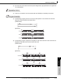
SAFETY PRECAUTIONS
(Always read these cautions before using the product)
Before using this product, please read this manual and the related manuals introduced in this manual, and pay
full attention to safety to handle the product correctly.
Please store this manual in a safe place and make it accessible when required. Always forward a copy of the
manual to the end user.
A-1
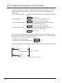
CONDITIONS OF USE FOR THE PRODUCT
(1) Although MELCO has obtained the certification for Product's compliance to the international safety
standards IEC61508, EN954-1/ISO13849-1 from TUV Rheinland, this fact does not guarantee that
Product will be free from any malfunction or failure. The user of this Product shall comply with any
and all applicable safety standard, regulation or law and take appropriate safety measures for the
system in which the Product is installed or used and shall take the second or third safety measures
other than the Product. MELCO is not liable for damages that could have been prevented by
compliance with any applicable safety standard, regulation or law.
(2) MELCO prohibits the use of Products with or in any application involving, and MELCO shall not be
liable for a default, a liability for defect warranty, a quality assurance, negligence or other tort and a
product liability in these applications.
(a) power plants,
(b) trains, railway systems, airplanes, airline operations, other transportation systems,
(c) hospitals, medical care, dialysis and life support facilities or equipment,
(d) amusement equipments,
(e) incineration and fuel devices,
(f) handling of nuclear or hazardous materials or chemicals,
(g) mining and drilling,
(h) and other applications where the level of risk to human life, health or property are elevated.
A-2
REVISIONS
*The manual number is given on the bottom left of the back cover.
Print Date
*Manual Number
Revision
Sep., 2006
SH(NA)-080628ENG-A First edition
Sep.,2007
SH(NA)-080628ENG-B
Partial corrections
Section 3.2, 5.2.3, 5.3.3, 5.4.1, 6.2.5, 6.3.1, 6.3.2, 6.4.1, INDEX
Apr.,2008
SH(NA)-080628ENG-C
Partial corrections
ABOUT MANUALS, Section 1.2, 3.2.2, 3.2.3, Chapter 4, Section 6.1.1, 6.1.2,
6.2.1, 6.2.2, 6.2.3, 6.2.4, 6.2.5, 6.2.6, 6.3.1, 6.3.2, 6.3.3, 6.3.4, 7.1.1, 7.1.2, 7.1.3,
7.1.4, 9.1.1, 9.1.4, 9.1.5, 9.1.6, 9.1.8, Appendix1.1, Appendix 2, Appendix3
May, 2011
SH(NA)-080628ENG-D
Partial corrections
ABOUT MANUALS, Section 1.2, 9.1.1, 9.1.4, 9.1.5, Appendix1.1, Appendix 2,
Appendix3
Japanese Manual Version SH-080610-D
This manual confers no industrial property rights or any rights of any other kind, nor does it confer any patent licenses.
Mitsubishi Electric Corporation cannot be held responsible for any problems involving industrial property rights which may
occur as a result of using the contents noted in this manual.
© 2006 MITSUBISHI ELECTRIC CORPORATION
A-3
INTRODUCTION
Thank you for choosing the Mitsubishi MELSEC-QS Series of Safety Programmable Logic Controllers.
Before using the equipment, please read this manual carefully to develop full familiarity with the functions and
performance of the QS series PLC you have purchased, so as to ensure correct use.
A copy of this manual should be forwarded to the end User.
CONTENTS
SAFETY PRECAUTIONS .................................................................................................................................A - 1
REVISIONS.......................................................................................................................................................A - 3
INTRODUCTION...............................................................................................................................................A - 4
CONTENTS ......................................................................................................................................................A - 4
ABOUT MANUALS ...........................................................................................................................................A - 7
1. GENERAL DESCRIPTION
1 - 1 to 1 - 4
1.1
Manuals Essential for Programming ................................................................................................ 1 - 2
1.2
Generic Terms and Abbreviations ................................................................................................... 1 - 3
2. INSTRUCTION TABLES
2 - 1 to 2 - 16
2.1
Types of Instructions........................................................................................................................ 2 - 2
2.2
How to Read Instruction Tables....................................................................................................... 2 - 3
2.3
Sequence Instruction ....................................................................................................................... 2 - 5
2.3.1
2.3.2
2.3.3
2.3.4
2.3.5
2.3.6
2.4
Basic Instructions............................................................................................................................. 2 - 9
2.4.1
2.4.2
2.4.3
2.4.4
2.5
Comparison operation instructions ........................................................................................... 2 - 9
Arithmetic operation instructions............................................................................................. 2 - 11
Data conversion instructions................................................................................................... 2 - 12
Data transfer instructions........................................................................................................ 2 - 13
Application Instructions .................................................................................................................. 2 - 14
2.5.1
2.6
Contact instructions .................................................................................................................. 2 - 5
Connection instructions ............................................................................................................ 2 - 6
Output instructions.................................................................................................................... 2 - 7
Master control instructions........................................................................................................ 2 - 7
Termination instruction ............................................................................................................. 2 - 8
Other instructions...................................................................................................................... 2 - 8
Logical operation instructions ................................................................................................. 2 - 14
QSCPU Dedicated Instruction ....................................................................................................... 2 - 16
2.6.1
Forced control stop instruction................................................................................................ 2 - 16
3. CONFIGURATION OF INSTRUCTIONS
3 - 1 to 3 - 18
3.1
Configuration of Instructions ............................................................................................................ 3 - 2
3.2
Designating Data ............................................................................................................................. 3 - 3
3.2.1
3.2.2
3.2.3
A-4
Using bit data............................................................................................................................ 3 - 3
Using word (16 bits) data.......................................................................................................... 3 - 4
Using double word (32 bits) data .............................................................................................. 3 - 6
3.3
Subset Processing........................................................................................................................... 3 - 9
3.4
Cautions on Programming (Operation Errors) ............................................................................... 3 - 10
3.5
Conditions for Execution of Instructions ........................................................................................ 3 - 12
3.6
Counting Step Number .................................................................................................................. 3 - 13
3.7
Operation when OUT, SET/RST, or PLS/PLF Instructions Use the Same Device........................ 3 - 14
4. HOW TO READ INSTRUCTIONS
5. SEQUENCE INSTRUCTIONS
5.1
Setting and resetting the master control (MC, MCR).............................................................. 5 - 38
Termination Instruction .................................................................................................................. 5 - 42
5.5.1
5.6
Out instructions (excluding timers, counters, and annunciators) (OUT) ................................. 5 - 17
Timers (OUT T,OUTH T) ........................................................................................................ 5 - 19
Counters (OUT C) .................................................................................................................. 5 - 23
Annunciator output (OUT F) ................................................................................................... 5 - 25
Setting devices (except for annunciators) (SET) .................................................................... 5 - 27
Resetting devices (except for annunciators) (RST) ................................................................ 5 - 29
Setting and resetting the annunciators (SET F, RST F) ......................................................... 5 - 31
Leading edge and trailing edge output (PLS, PLF) ................................................................ 5 - 33
Bit device output reverse (FF) ................................................................................................ 5 - 36
Master Control Instructions............................................................................................................ 5 - 38
5.4.1
5.5
Ladder block series connections and parallel connections (ANB, ORB) .................................. 5 - 7
Operation results push, read, pop (MPS, MRD, MPP) ............................................................. 5 - 9
Operation results inversion (INV) ........................................................................................... 5 - 12
Operation result pulse conversion (MEP, MEF) ..................................................................... 5 - 14
Pulse conversion of edge relay operation results (EGP, EGF) .............................................. 5 - 15
Output Instruction .......................................................................................................................... 5 - 17
5.3.1
5.3.2
5.3.3
5.3.4
5.3.5
5.3.6
5.3.7
5.3.8
5.3.9
5.4
Operation start, series connection, parallel connection (LD, LDI, AND, ANI, OR, ORI) ........... 5 - 2
Pulse operation start, pulse series connection, pulse parallel connection
(LDP, LDF, ANDP, ANDF, ORP, ORF) .................................................................................... 5 - 5
Connection Instructions ................................................................................................................... 5 - 7
5.2.1
5.2.2
5.2.3
5.2.4
5.2.5
5.3
End sequence program (END) ............................................................................................... 5 - 42
Other Instructions .......................................................................................................................... 5 - 43
5.6.1
No-operation (NOP, NOPLF, PAGE n)................................................................................... 5 - 43
6. BASIC INSTRUCTIONS
6.1
6 - 1 to 6 - 38
Comparison Operation Instruction ................................................................................................... 6 - 2
6.1.1
6.1.2
6.2
5 - 1 to 5 - 46
Contact Instruction........................................................................................................................... 5 - 2
5.1.1
5.1.2
5.2
4 - 1 to 4 - 4
BIN 16-bit data comparisons (= , <> , >, <= , <, >=) ................................................................. 6 - 2
BIN 32-bit data comparisons (D=, D<>, D>, D<=, D<, D>=) .................................................... 6 - 4
Arithmetic Operation Instructions..................................................................................................... 6 - 6
6.2.1
6.2.2
6.2.3
6.2.4
BIN 16-bit addition and subtraction operations (+(P), –(P))...................................................... 6 - 6
BIN 32-bit addition and subtraction operations (D+(P), D–(P)) .............................................. 6 - 10
BIN 16-bit multiplication and division operations (*(P), /(P))................................................... 6 - 14
BIN 32-bit multiplication and division operations (D*(P), D/(P)) ............................................. 6 - 16
A-5
6.2.5
6.2.6
6.3
Data Conversion Instructions......................................................................................................... 6 - 22
6.3.1
6.3.2
6.3.3
6.4
Incrementing and decrementing 16-bit BIN data (INC(P), DEC(P)) ....................................... 6 - 18
Incrementing and decrementing 32-bit BIN data (DINC(P), DDEC(P)) .................................. 6 - 20
Conversion from BIN data to 4-digit and 8-digit BCD (BCD(P), DBCD(P)) ............................ 6 - 22
Conversion from BCD 4-digit and 8-digit data to BIN data (BIN(P), DBIN(P))........................ 6 - 24
Complement of 2 of BIN 16- and 32-bit data (sign reversal) (NEG(P), DNEG(P)) ................. 6 - 27
Data Transfer Instructions ............................................................................................................. 6 - 29
6.4.1
6.4.2
6.4.3
6.4.4
16-bit and 32-bit data transfers (MOV(P), DMOV(P))............................................................. 6 - 29
16-bit and 32-bit negation transfers (CML(P), DCML(P)) ....................................................... 6 - 31
Block 16-bit data transfers (BMOV(P)) ................................................................................... 6 - 34
Identical 16-bit data block transfers (FMOV(P)) ..................................................................... 6 - 36
7. APPLICATION INSTRUCTIONS
7.1
Logical Operation Instructions ......................................................................................................... 7 - 2
7.1.1
7.1.2
7.1.3
7.1.4
Logical products with 16-bit and 32-bit data (WAND(P), DAND(P)) ......................................... 7 - 3
Logical sums of 16-bit and 32-bit data (WOR(P), DOR(P)) ...................................................... 7 - 8
16-bit and 32-bit exclusive OR operations (WXOR(P), DXOR(P)) ......................................... 7 - 12
16-bit and 32-bit data exclusive NOR operations (WXNR(P), DXNR(P)) ............................... 7 - 16
8. QSCPU DEDICATED INSTRUCTIONS
8.1
8 - 1 to 8 - 4
Forced Control Stop Instruction (S.QSABORT)............................................................................... 8 - 2
9. ERROR CODE
9.1
7 - 1 to 7 - 20
9 - 1 to 9 - 46
Error Code List................................................................................................................................. 9 - 2
9.1.1
9.1.2
9.1.3
9.1.4
9.1.5
9.1.6
9.1.7
9.1.8
Error codes ............................................................................................................................... 9 - 3
Reading an error code .............................................................................................................. 9 - 3
Error code list (1000 to 1999) ................................................................................................... 9 - 4
Error code list (2000 to 2999) ................................................................................................. 9 - 10
Error code list (3000 to 3999) ................................................................................................. 9 - 16
Error code list (4000 to 4999) ................................................................................................. 9 - 26
Error code list (5000 to 5999) ................................................................................................. 9 - 30
Error code list (8000 to 9000) ................................................................................................. 9 - 32
APPENDICIES
Appendix 1
App - 1 to App - 34
OPERATION PROCESSING TIME...................................................................................App- 2
Appendix 1.1
Definition ...................................................................................................................App- 2
Appendix 1.2
Operation Processing Time .......................................................................................App- 3
Appendix 2 SPECIAL RELAY LIST ....................................................................................................App- 11
Appendix 3
INDEX
A-6
SPECIAL REGISTER LIST .............................................................................................App- 16
Index - 1 to Index - 5
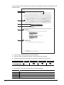
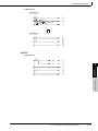
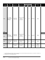
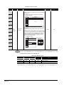
ABOUT MANUALS
Introduction Manual
Read the following manual before designing and constructing a safety system.
Manual Number
Manual Name
(Model Code)
Safety Application Guide
Explains the overview, construction method, laying and wiring examples, and application programs of the safety-related
SH-080613ENG
(13JR90)
system.
(Sold separately)
Related Manuals
The manuals related to this product are listed below.
Please place an order as needed.
Manual Number
Manual Name
(Model Code)
QSCPU User’s Manual (Hardware Design, Maintenance and Inspection)
SH-080626ENG
Explains the specifications of the QSCPU, safety power supply module, and safety base unit.
(Sold separately)
QSCPU User's Manual (Function Explanation, Program Fundamentals)
Explains the functions, programming methods, devices and others that are necessary to create programs with the QSCPU.
(Sold separately)
(13JR92)
SH-080627ENG
(13JR93)
CC-Link Safety System Master Module User's Manual
Explains the specifications, procedures and settings before operation, parameter settings, and troubleshooting of the
SH-080600ENG
(13JR88)
QS0J61BT12 CC-Link Safety system master module.
(Sold separately)
CC-Link Safety System Remote I/O Module User's Manual
Explains the specifications, procedures and settings before operation, parameter settings, and troubleshooting of the CC-Link
SH-080612ENG
(13JR89)
Safety system remote I/O modules.
(Sold separately)
MELSEC-QS CC-Link IE Field Network Master/Local Module User's Manual
Explains the system configuration, performance specifications, functions, handling, wiring, and troubleshooting of the CC-Link
SH-080969ENG
13JZ53
IE Field Network master/local module (with safety functions).
(Sold separately)
CC-Link IE Controller Network Reference Manual
Explains the system configuration, specifications, functions, handling, wiring, and troubleshooting of CC-Link IE Controller
SH-080668ENG
(13JV16)
Network.
(Sold separately)
Q corresponding MELSECNET/H Network System Reference Manual (PLC to PLC network)
Explains the specifications, procedures and settings before operation, parameter settings, programming, and troubleshooting
SH-080049
(13JF92)
of a MELSECNET/H network system for PLC to PLC network.
(Sold separately)
Q Corresponding Ethernet Interface Module User’s Manual (Basic)
Explains the specifications, procedures for data communication with external devices, line connection (open/close), fixed
SH-080009
(13JL88)
buffer communication, random access buffer communication, and troubleshooting of the Ethernet module.
(Sold separately)
A-7
Manual Number
Manual Name
(Model Code)
Q Corresponding Ethernet Interface Module User’s Manual (Application)
Explains the e-mail function, programmable controller CPU status monitoring function, communication function via CC-Link IE
Controller Network, MELSECNET/H or MELSECNET/10, communication function using the data link instructions, file transfer
function (FTP server) of the Ethernet module.
SH-080010
(13JL89)
(Sold separately)
Q Corresponding MELSEC Communication Protocol Reference Manual
Explains the communication methods and control procedures using the MC protocol, which is used by external devices to read
and write data of the programmable controller CPU via the serial communication module or Ethernet module.
SH-080008
(13JF89)
(Sold separately)
GX Developer Version 8 Operating Manual
Explains the online functions of the GX Developer, such as the programming, printout, monitoring, and debugging methods.
(Sold separately)
GX Developer Version 8 Operating Manual (Safety Programmable Controller)
Explains the GX Developer functions added and modified for the compatibility with the safety programmable controller.
(Sold separately)
SH-080373E
(13JU41)
SH-080576ENG
(13JU53)
Remark
Printed materials are separately available for single item purchase. Order the
manual by quoting the manual number on the table above (Model code).
A-8
APPLICATION
INSTRUCTIONS
BASIC
INSTRUCTIONS
SEQUENCE
INSTRUCTIONS
HOW TO READ
INSTRUCTIONS
CONFIGURATION
OF INSTRUCTIONS
1
GENERAL
DESCRIPTION
GENERAL
DESCRIPTION
INSTRUCTION TABLES
1
2
3
4
5
6
7
1-1
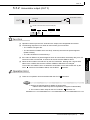
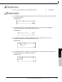
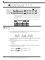
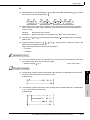
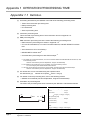
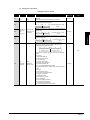
This manual describes the instructions required to execute programming of the QSCPU.
1.1 Manuals Essential for Programming
Before reading this manual, check the functions, programming methods, devices and others that
are necessary to create programs with the QSCPU in the manuals below:
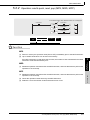
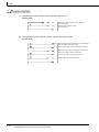
• QSCPU User’s Manual (Function Explanation, Program Fundamentals)
QSCPU User's Manual
(Function Explanation,
Programming
Fundamentals)
Explains the functions,
programming methods,
devices and others that
are necessary to create
programs with the QSCPU.
This manual
QSCPU Programming
Manual (Common
Describes the instructions
Instructions)
used by QSCPU.
1-2
1.1 Manuals Essential for Programming
1
GENERAL
DESCRIPTION
1.2 Generic Terms and Abbreviations
This manual describes the QS series CPU module using the following generic terms and
abbreviations, unless otherwise specified.
Generic term/Abbreviation
Description
Generic term for safety CPU module, safety power supply module, safety
Safety PLC
main base unit, CC-Link safety master module, CC-Link safety remote I/O
module, and CC-Link IE Field Network master/local module (with safety
functions).
Generic term of each module for MELSEC-Q series, MELSEC-L series,
Standard PLC
MELSEC-QnA series, MELSEC-A series and MELSEC-FX series. (Used
for distinction from safety PLC.)
QS Series
Abbreviation for Mitsubishi Safety PLC MELSEC-QS Series
QS001CPU
Abbreviation for QS001CPU-type safety CPU module
CPU Module
Other name for QS001CPU
GX Developer
QS0J61BT12
Generic product name for product models SW8D5C-GPPW-E, SW8D5CGPPW-EA, SW8D5C-GPPW-EV and SW8D5C-GPPW-EVA
Abbreviation for QS0J61BT12-type CC-Link Safety system master
module
CC-Link Safety
Abbreviation for the CC-Link Safety system
CC-Link Safety master module
Other name for QS0J61BT12
QS0J65BTS2-8D
Abbreviation for the QS0J65BTS2-8D CC-Link Safety remote I/O module
QS0J65BTS2-4T
Abbreviation for the QS0J65BTS2-4T CC-Link Safety remote I/O module
QS0J65BTB2-12DT
CC-Link Safety remote I/O module
Abbreviation for the QS0J65BTB2-12DT CC-Link Safety remote I/O
module
Generic term for the QS0J65BTS2-8D, QS0J65BTS2-4T, and
QS0J65BTB2-12DT
CC-Link IE Field Network master/local
Abbreviation for MELSEC-QS series CC-Link IE Field Network master/
module (with safety functions)
local module
Abbreviation for the QJ71GP21-SX CC-Link IE Controller Network
CC-Link IE Controller Network module
module and QJ71GP21S-SX CC-Link IE Controller Network module (with
external power supply function)
MELSECNET/H
MELSECNET/H module
Ethernet
Ethernet module
Abbreviation for the MELSECNET/H network system
Abbreviation for the QJ71LP21-25, QJ71LP21S-25, QJ71LP21G,
QJ71BR11 MELSECNET/H network module
Abbreviation for the Ethernet network system
Abbreviation for the QJ71E71-100, QJ71E71-B5, QJ71E71-B2 Ethernet
interface module
Generic term for the CC-Link Safety master module, CC-Link IE Field
Intelligent function module
Network master/local module (with safety functions), CC-Link IE
Controller Network module, MELSECNET/H module, and Ethernet
module
1.2 Generic Terms and Abbreviations
1-3
MEMO
1-4
APPLICATION
INSTRUCTIONS
BASIC
INSTRUCTIONS
SEQUENCE
INSTRUCTIONS
HOW TO READ
INSTRUCTIONS
CONFIGURATION
OF INSTRUCTIONS
2
GENERAL
DESCRIPTION
INSTRUCTION
TABLES
INSTRUCTION TABLES
1
2
3
4
5
6
7
2-1
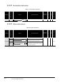
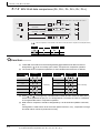
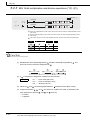
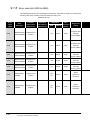
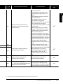
2.1 Types of Instructions
The major types of safety CPU module instructions are sequence instructions, basic instructions,
application instructions, and QSCPU dedicated instructions as shown in Table 2.1
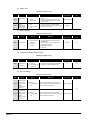
Table 2.1 Types of Instructions
Types of Instructions
Contact instruction
Connection instructions
Sequence
instruction
Bit device output, output reversal
Termination instruction
Program termination
Other instructions
Instructions such as no operation which do not fit in the above categories
Arithmetic operation instruction
instructions
BCD
BIN conversion
instruction
instructions
operation results
Master control
Basic
Chapter
Ladder block connection, store/read operation results, creation of pulses from
Master control instruction
instruction
Reference
Operation start, series connection, parallel connection
Output instruction
Comparison operation
Application
Meaning
Comparisons such as
,
5
,
Addition, subtraction, multiplication or division of BIN
6
Conversion from BCD to BIN and from BIN to BCD
Data transfer instruction
Transmits designated data
Logical operation instructions
Logical operations such as logical sum, logical product, etc.
7
QSCPU dedicated instruction
Forced control stop
8
QSCPU
dedicated
instruction
2-2
2.1 Types of Instructions
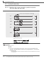
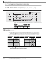
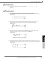
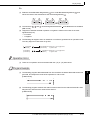
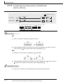
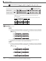
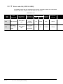
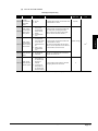
2.2 How to Read Instruction Tables
The instruction tables found from Section 2.3 to 2.6 have been made according to the following
format:
2
+
+
S
+P
+P
S D
1)
+
+
S1 S2 D
+P
+P
S1 S2 D
(S1)+(S2)
2)
Condition
D
(D)+(S)
BIN
16-bit
addition and
subtraction
operations
Execution
INSTRUCTION TABLES
Processing Details
See for Description
Symbol
Subset
Category
Number of Basic Steps
Instruction Symbols
Table 2.2 How to Read Instruction Tables
(D)
(D)
3)
4)
5)
3
6-6
4
6-8
6)
7)
8)
Description
1) . . . . . Classifies instructions according to their application.
2) . . . . . Indicates the instruction symbol used in a program.
Instruction code is built around the 16-bit instruction.
The following notations are used to mark 32-bit instructions, instructions executed only
at the leading edge of OFF to ON.
• 32-bit instruction . . The letter "D" is added to the first line of the instruction.
Example
+
D+
16-bit
instruction
32-bit
instruction
• Instructions executed only at the leading edge of OFF to ON
. . . . . . . . . . . . . . . The letter "P" is added to the end of the instruction.
Example
+
Instruction
executed during ON
+P
Instruction executed only at
the leading edge of OFF to ON
2.2 How to Read Instruction Tables
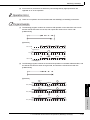
2-3
3) . . . . .Shows symbol diagram on the ladder.
+
S1 S2 D
+
S D
Indicates destination.
Indicates destination.
Indicates source.
Indicates source.
Indicates instruction symbol.
Indicates instruction symbol.
Fig. 2.1 Shows Symbol Diagram on the Ladder
Destination . . . . . . Indicates where data will be sent after operation.
Source . . . . . . . . . Stores data prior to operation.
4) . . . . .Indicates the type of processing that is performed by individual instructions.
(D)+(S)
(D)
Indicates 16 bits.
(D+1, D)+(S+1, S)
Indicates
16 bits.
(D+ 1,D)
Indicates
16 bits.
Indicates 32 bits.
D+1
Upper 16 bits
D
Lower 16 bits
Fig. 2.2 Type of Processing Performed by Individual Instructions
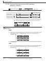
5) . . . . .The details of conditions for the execution of individual instructions are as follows:
Symbol
No symbol
recorded
Execution Condition
Instruction executed under normal circumstances, with no regard to the ON/OFF status of conditions prior to
the instruction.
If the precondition is OFF, the instruction will conduct OFF processing.
Executed during ON; instruction is executed only while the precondition is ON. If the preconditions is OFF,
the instruction is not executed, and no processing is conducted.
Executed once at ON; instruction executed only at leading edge when precondition goes from OFF to ON.
Following execution, instruction will not be executed and no processing conducted even if condition remains
ON.
Executed during OFF; instruction is executed only while the precondition is OFF. If the precondition is ON,
the instruction is not executed, and no processing is conducted.
Executed once at OFF; instruction executed only at trailing edge when precondition goes from ON to OFF.
Following execution, instruction will not be executed and no processing conducted even if condition remains
OFF.
6) . . . . .Indicates the basic number of steps for individual instructions.
See 3.6 for a description of the number of steps.
7) . . . . .The
mark indicates instructions for which subset processing is possible.
See Section 3.3 for details on subset processing.
8) . . . . .Indicates the page numbers where the individual instructions are explained.
2-4
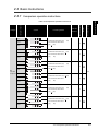
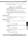
2.2 How to Read Instruction Tables
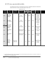
2.3 Sequence Instruction
Contact instructions
2
LD
LDI
AND
ANI
OR
Contact
ORI
Condition
See for Description
Execution
Processing Details
Subset
Symbol
Number of Basic Steps
Category
Instruction Symbols
Table 2.3 Contact Instructions
• Starts logic operation
(Starts a contact logic operation)
• Starts logical NOT operation
(Starts b contact logic operation)
• Logical product
(a contact series connection)
• Logical product NOT
1
5-2
1
5-5
(b contact series connection)
• Logical sum
(a contact parallel connection)
• Logical sum NOT
(b contact parallel connection)
LDP
• Starts leading edge pulse operation
LDF
• Starts trailing edge pulse operation
ANDP
• Leading edge pulse series connection
ANDF
• Trailing edge pulse series connection
ORP
• Leading edge pulse parallel connection
ORF
• Trailing edge pulse parallel connection
2.3 Sequence Instruction
2.3.1 Contact instructions
2-5
INSTRUCTION TABLES
2.3.1
2.3.2
Connection instructions
Execution
Condition
See for Description
Processing Details
Subset
Symbol
Number of Basic Steps
Category
Instruction Symbols
Table 2.4 Connection Instructions
1
-
5-7
1
-
5-9
1
-
5-12
1
-
5-14
-
5-15
• AND between logical blocks
ANB
(Series connection between logical
ANB
blocks)
• OR between logical blocks
ORB
ORB
MPS
MRD
Connection
blocks)
• Memory storage of operation results
• Read of operation results stored with
MPS
MPS instruction
MRD
MPP
(Series connection between logical
• Read and reset of operation results
MPP
stored with MPS instruction
INV
• Inversion of operation result
• Conversion of operation result to leading
MEP
edge pulse
• Conversion of operation result to trailing
MEF
edge pulse
• Conversion of operation result to leading
EGP
Vn
edge pulse
1
(Stored at Vn)
• Conversion of operation result to trailing
EGF
Vn
edge pulse
(Stored at Vn)
2-6
2.3 Sequence Instruction
2.3.2 Connection instructions
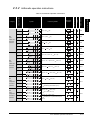
2
2.3.3
Output instructions
5-17
OUT
• Device output
*1
-
5-19
5-23
5-25
• Set device
*2
RST
RST
D
• Reset device
*2
PLS
PLS
D
PLF
PLF
D
FF
FF
D
5-27
*1
-
*1
-
2
-
5-33
2
-
5-36
See for Description
D
Subset
SET
Number of Basic Steps
Output
SET
-
5-38
5-31
5-29
5-31
• Generates 1 cycle program pulse at
leading edge of input signal.
• Generates 1 cycle program pulse at
trailing edge of input signal.
• Reversal of device output
*1: The number of steps may vary depending on the device being used.
See description pages of individual instructions for number of steps.
*2: The
2.3.4
execution condition applies only when an annunciator (F) is in use.
Master control instructions
Category
Master
control
Instruction Symbols
Table 2.6 Master Control Instructions
MC
MCR
Symbol
MC
MCR
Processing Details
n D
n
Execution
Condition
• Starts master control
2
• Resets master control
1
2.3 Sequence Instruction
2.3.3 Output instructions
2-7
2
INSTRUCTION TABLES
Condition
See for Description
Execution
Processing Details
Subset
Symbol
Number of Basic Steps
Category
Instruction Symbols
Table 2.5 Output Instructions
2.3.5
Termination instruction
Subset
See for Description
1
-
5-42
See for Description
Condition
• Termination of sequence program
END
2.3.6
Execution
Subset
Termination END
Processing Details
Number of Basic Steps
Symbol
Number of Basic Steps
Category
Instruction Symbols
Table 2.7 Termination Instruction
1
-
5-43
Other instructions
Category
Instruction Symbols
Table 2.8 Other Instructions
Symbol
NOP
–––––––
NOPLF
Processing Details
• Ignored
NOPLF
(To change pages during printouts)
• Ignored
PAGE
n
(Subsequent programs will be controlled
from step 0 of page n)
2-8
Condition
• Ignored (For program deletion or space)
No-operation
PAGE
Execution
2.3 Sequence Instruction
2.3.5 Termination instruction
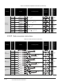
2.4 Basic Instructions
Comparison operation instructions
2
LD =
S1 S2
AND =
S1 S2
OR =
• Conductive status when (S1)
See for Description
Condition
(S2)
3
• Non-conductive status when
(S2)
S1 S2
S1 S2
AND<>
S1 S2
• Conductive status when (S1)
(S2)
3
• Non-conductive status when
(S1)
(S2)
S1 S2
LD>
S1 S2
AND>
S1 S2
OR>
Execution
Processing Details
(S1)
LD<>
OR<>
BIN
Symbol
Subset
Category
Number of Basic Steps
Instruction Symbols
Table 2.9 Comparison Operation Instructions
• Conductive status when (S1)
(S2)
3
• Non-conductive status when
(S1)
(S2)
S1 S2
6-2
16-bit data
comparisons LD<=
AND<=
OR<=
S1 S2
S1 S2
3
(S2)
S1 S2
S1 S2
AND<
S1 S2
• Conductive status when (S1)
(S2)
3
• Non-conductive status when
(S1)
(S2)
S1 S2
LD>=
S1 S2
AND>=
S1 S2
OR>=
(S2)
• Non-conductive status when
(S1)
LD<
OR<
• Conductive status when (S1)
• Conductive status when (S1)
(S2)
• Non-conductive status when
(S1)
3
(S2)
S1 S2
2.4 Basic Instructions
2.4.1 Comparison operation instructions
2-9
INSTRUCTION TABLES
2.4.1
LDD =
D
S1 S2
ANDD =
D
S1 S2
D
S1 S2
LDD<>
D
S1 S2
ANDD<>
D
S1 S2
(S1+1, S1)
(S2+1, S2)
(S1+1, S1)
D
S1 S2
LDD>
D
S1 S2
ANDD>
D
S1 S2
• Conductive status when
(S1+1, S1)
(S2+1, S2)
(S1+1, S1)
ORD>
D
S1 S2
3
(S2+1, S2)
• Conductive status when
(S1+1, S1)
(S2+1, S2)
• Non-Conductive status when
BIN
3
(S2+1, S2)
• Non-Conductive status when
ORD<>
Condition
• Conductive status when
• Non-Conductive status when
ORD =
Execution
(S1+1, S1)
3
(S2+1, S2)
6-4
32-bit data
comparisons LDD<=
ANDD<=
D
S1 S2
D
S1 S2
• Conductive status when
(S1+1, S1)
(S2+1, S2)
• Non-Conductive status when
ORD<=
D
S1 S2
LDD<
D
S1 S2
ANDD<
D
S1 S2
(S1+1, S1)
ORD<
• Conductive status when
(S1+1, S1)
(S1+1, S1)
D
S1 S2
LDD>=
D
S1 S2
ANDD>=
D
S1 S2
(S2+1, S2)
D
S1 S2
2.4 Basic Instructions
2.4.1 Comparison operation instructions
3
(S2+1, S2)
• Conductive status when
(S1+1, S1)
(S2+1, S2)
• Non-Conductive status when
ORD>=
3
(S2+1, S2)
• Non-Conductive status when
2-10
See for Description
Processing Details
Subset
Symbol
Number of Basic Steps
Category
Instruction Symbols
Table 2.9 Comparison Operation Instructions (Continued)
(S1+1, S1)
(S2+1, S2)
3
2.4.2
Arithmetic operation instructions
+
+
S D
+P
+P
S D
• (D) + (S)
BIN
16-bit
+
+
S1 S2 D
+P
+P
S1 S2 D
• (S1) + (S2)
Execution
Condition
(D)
(D)
3
6-6
4
6-8
3
6-6
4
6-8
3
6-10
4
6-12
3
6-10
4
6-12
addition and
subtraction
–
S D
• (D)
operations
–P
P
–
(S)
(D)
S D
S1 S2 D
• (S1)
–P
(S2)
(D)
S1 S2 D
P
D+
D+
S D
D+P
D+P
S D
• (D+1, D) + (S+1, S)
BIN
32-bit
D+
D+
S1 S2 D
D+P
D+P
S1 S2 D
D–
D
S D
D–P
D P
S D
(D+1, D)
• (S1+1, S1) + (S2+1, S2)
(D+1, D)
addition and
subtraction
operations
• (D+1, D)
D–
D
D–P
D
*
*
S1 S2 D
16-bit
*P
*P
S1 S2 D
and division
/
/
S1 S2 D
operations
D/P
/P
S1 S2 D
BIN
D*
D*
S1 S2 D
32-bit
D*P
D*P
S1 S2 D
D/
D/
S1 S2 D
D/P
D/P
S1 S2 D
P
operations
(D+1, D)
(S2)
(D+1,D)
4
6-14
multiplication
and division
(S2+1, S2)
S1 S2 D
• (S1)
multiplication
(D+1, D)
S1 S2 D
• (S1+1, S1)
BIN
(S+1, S)
• (S1) / (S2)
Quotient(D), Remainder (D+1)
• (S1+1, S1)
(S2+1, S2)
(D+3, D+2, D+1, D)
4
4
6-16
• (S1+1, S1) / (S2+1, S2)
Quotient (D+1, D), Remainder (D+3,
4
D+2)
2.4 Basic Instructions
2.4.2 Arithmetic operation instructions
2-11
2
INSTRUCTION TABLES
Processing Details
See for Description
Symbol
Subset
Category
Number of Basic Steps
Instruction Symbols
Table 2.10 Arithmetic Operation Instructions
Processing Details
INC
INC
D
INCP
INCP
D
DINC
DINC
D
DINCP
DINCP
D
DEC
DEC
D
DECP
DECP
D
DDEC
DDEC
D
DDECP
DDECP
D
• (D) + 1
increment
• (D)
1
(D+1, D)
(D)
• (D+1, D)
2.4.3
Condition
(D)
• (D+1, D) + 1
BIN data
Execution
1
(D+1, D)
See for Description
Symbol
Subset
Category
Number of Basic Steps
Instruction Symbols
Table 2.10 Arithmetic Operation Instructions (Continued)
2
6-18
2
6-20
2
6-18
2
6-20
Data conversion instructions
BCD
conversions
BIN
conversions
to 2
2-12
BCD
S D
BCDP
BCDP
S D
DBCD
DBCD
S D
DBCDP
DBCDP
S D
BIN
BIN
S D
. (S) BIN conversion (D)
BINP
BINP
S D
BCD (0 to 9999)
DBIN
DBIN
S D
DBINP
DBINP
S D
. (S) BCD conversion (D)
Condition
See for Description
Execution
Subset
Processing Details
BCD
3
BIN (0 to 9999)
6-22
. (S+1,S)
BCD conversion
( D +1,D)
3
BIN (0 to 99999999)
3
6-24
NEG
Complement
Symbol
Number of Basic Steps
Category
Instruction Symbols
Table 2.11 Data Conversion Instructions
NEG
D
NEGP
NEGP
D
DNEG
DNEG
D
DNEGP
DNEGP
D
. (S+1, S)
BIN conversion
(D +1,D)
3
BCD (0 to 99999999)
. (D)
(D)
2
–
BIN data
6-27
2.4 Basic Instructions
2.4.3 Data conversion instructions
. (D+1, D)
(D+1,D)
BIN data
2
–
2.4.4
Data transfer instructions
MOV
S D
MOVP
MOVP
S D
DMOV
DMOV
S D
DMOVP
DMOVP
S D
CML
CML
S D
transfer
CMLP
CMLP
S D
32-bit data
DCML
DCML
S D
DCMLP
DCMLP
S D
transfer
⋅ (S)
( D)
See for Description
Condition
*1
6-29
32-bit data
transfer
16-bit data
⋅ (S+1,S)
⋅ (S)
negation
*2
( D+1,D)
*1
( D)
6-31
⋅ (S+1,S)
negation
transfer
Block
transfer
Multiple
transfers of
same data
block
BMOV
BMOV
S D n
BMOVP
BMOVP
S D n
FMOV
FMOV
S D n
(S)
FMOVP
(D)
n
(D)
(S)
FMOVP
*2
( D+1,D)
S D n
n
4
6-34
4
6-36
*1: The number of steps may vary depending on the device being used.
Number of
Device
· Word device:
· Bit device:
Steps
Internal device
Devices whose device Nos. are multiples of 16 and whose digit
designation is K4
· Constant:
2
No limitations
3
Devices other than above
*2: The number of steps may vary depending on the device being used.
Number of
Device
· Word device:
· Bit device:
Internal device
Devices whose device Nos. are multiples of 16 and whose digit
designation is K8
· Constant:
Steps
No limitations
Devices other than above
3
Note 1)
3 Note 1)
Note 1) The number of steps may increase due to the conditions described in 3.6.
2.4 Basic Instructions
2.4.4 Data transfer instructions
2-13
2
INSTRUCTION TABLES
MOV
16-bit data
Execution
Processing Details
Subset
Symbol
Number of Basic Steps
Category
Instruction Symbols
Table 2.12 Data Transfer Instructions
2.5 Application Instructions
2.5.1
Logical operation instructions
WAND
S D
WANDP
WANDP
S D
⋅ (D)
WAND
WAND
S1 S2 D
WANDP
WANDP
S1 S2 D
⋅ (S1)
Logical
product
DAND
DAND
(S2)
DAND
DANDP
DAND
(S+1,S)
DANDP
S1 S2 D
WOR
WOR
S D
WORP
WORP
S D
WOR
WOR
S1 S2 D
WORP
WORP
S1 S2 D
⋅ (S1)
sum
DOR
DOR
(S2)
DOR
DORP
S1 S2 D
WXOR
WXOR
S D
WXORP
WXORP
S D
WXOR
WXOR
S1 S2 D
WXORP
WXORP
S1 S2 D
DXOR
DXOR
DXORP
DXOR
(S2)
DXORP
(S+1,S)
(D+1,D)
S D
S1 S2 D
⋅ (S1+1,S1)
DXORP
(D)
S D
DXORP
DXOR
(D+1,D)
(D)
(S)
⋅ (D+1,D)
(S2+1,S2)
(D+1,D)
S1 S2 D
*1: The number of steps may increase due to the conditions described in 3.6.
2-14
2.5 Application Instructions
2.5.1 Logical operation instructions
Condition
3
7-3
4
7-5
*1
3
*1
4
7-3
7-5
3
7-8
4
7-10
*1
3
*1
(S2+1,S2)
S1 S2 D
⋅ (S1)
OR
(D+1,D)
S D
⋅ (D)
Exclusive
(S+1,S)
⋅ (S1+1,S1)
DORP
(D)
S D
DORP
DOR
(D+1,D)
(D)
(S)
⋅ (D+1,D)
DORP
(S2+1,S2)
S1 S2 D
⋅ (D)
Logical
(D+1,D)
S D
⋅ (S1+1,S1)
DANDP
(D)
S D
⋅ (D+1,D)
DANDP
(D)
(S)
Execution
See for Description
WAND
Processing Details
Subset
Symbol
Number of Basic Steps
Category
Instruction Symbols
Table 2.13 Logical Operation Instructions
4
7-8
7-10
3
7-12
4
7-14
*1
3
*1
4
7-12
7-14
S D
WXNRP
WXNRP
S D
⋅ (D)
NON
exclusive
logical
sum
WXNR
WXNR
S1 S2 D
WXNRP
WXNRP
S1 S2 D
⋅ (S1)
DXNR
DXNR
DXNR
(S2)
DXNRP
(S+1,S)
(D+1,D)
S D
S1 S2 D
⋅ (S1+1,S1)
DXNRP
(D)
S D
DXNRP
DXNR
(D)
(S)
⋅ (D+1,D)
DXNRP
Condition
(S2+1,S2)
(D+1,D)
S1 S2 D
3
7-16
4
7-18
*1
3
*1
4
7-16
7-18
*1: The number of steps may increase due to the conditions described in 3.6.
2.5 Application Instructions
2.5.1 Logical operation instructions
2-15
2
INSTRUCTION TABLES
WXNR
Execution
See for Description
WXNR
Processing Details
Subset
Symbol
Number of Basic Steps
Category
Instruction Symbols
Table 2.13 Logical Operation Instructions (Continued)
2.6 QSCPU Dedicated Instruction
2.6.1
Forced control stop instruction
control
• Stops program execution.
S.QSABORT
S.QSABORT S
stop
• Places safety CPU module in the stop error
state.
*1: 8 steps when a constant is used.
2-16
2.6 QSCPU Dedicated Instruction
2.6.1 Forced control stop instruction
Execution
Condition
*1
7
See for Description
Forced
Processing Details
Subset
Symbol
Number of Basic Steps
Category
Instruction Symbols
Table 2.14 Forced Control Stop Instruction
–
8-2
APPLICATION
INSTRUCTIONS
BASIC
INSTRUCTIONS
SEQUENCE
INSTRUCTIONS
HOW TO READ
INSTRUCTIONS
CONFIGURATION
OF INSTRUCTIONS
3
GENERAL
DESCRIPTION
CONFIGURATION OF
INSTRUCTIONS
INSTRUCTION TABLES
1
2
3
4
5
6
7
3-1
3.1 Configuration of Instructions
Most safety CPU module instructions consist of an instruction part and a device part.
Each part is used for the following purpose:
• Instruction part .. Indicates the function of the instruction.
• Device part ........ Indicates the data that is to be used with the instruction.
The device part is classified into source data, destination data, and number of devices.
(1) Source (S)
(a) Source is the data used for operations.
(b) The following source types are available, depending on the designated device:
• Constant ............................................... Designates a numeric value to be used in the
operation.
This is set when the program is created, and
cannot be changed during the execution of
the program.
• Bit devices and word devices ............... Designates the device that stores the data to
be used in the operation.
Data must be stored in the designated
device until the operation is executed.
By changing the data stored in a designated
device during program execution, the data to
be used in the instruction can be changed.
(2) Destination (D)
(a) The destination stores the data after the operation has been conducted.
However, some instructions require storing the data to be used in an operation at the
destination prior to the operation execution.
Example An addition instruction involving BIN 16-bit data
+
S
D
S1
+
Stores the data needed for operation
prior to the actual operation.
S2
D
Stores only the operation results.
(b) A device for the data storage must always be set to the destination.
(3) Number of devices and number of transfers (n)
(a) The number of devices and number of transfers designate the numbers of devices and
transfers used by instructions involving multiple devices.
Example Block transfer instruction
BMOV
S
D
n
Designates the number of transfers
transferred by a BMOV instruction.
(b) The number of devices or number of transfers can be set between 0 and 32767.
However, if the number is 0, the instruction will be a no-operation instruction.
3-2
3.1 Configuration of Instructions
3.2 Designating Data
The following three types of data can be used with safety CPU module instructions:
Bit Data
Data that can be handled
by safety CPU module
...Section 3.2.1
Numeric data
Integer data
Word data
...Section 3.2.2
Double word data ...Section 3.2.3
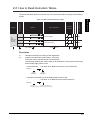
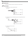
Using bit data
3
CONFIGURATION
OF INSTRUCTIONS
3.2.1
Bit data is data used in one-bit units, such as for contact points or coils.
"Bit devices" and "Bit designated word devices" can be used as bit data.
(1) When using bit devices
Bit devices are designated in one-point units.
The 1 point M0 is
designated
M0
SET
Y10
The 1 point Y10 is
designated
(2) Using word devices
(a) Word devices enable the use of a designated bit number 1/0 as bit data by the
designation of that bit number.
b15
Word device
b0
1/0 1/0 1/0 1/0 1/0 1/0 1/0 1/0 1/0 1/0 1/0 1/0 1/0 1/0 1/0 1/0
Each bit can use 1 as ON, 0 as OFF.
(1=ON, 0=OFF).
(b) Word device bit designation is done by designating " Word device . Bit No. ".
(Designation of bit numbers is done in hexadecimal.)
For example, bit 5 (b5) of D0 is designated as D0.5, and bit 10 (b10) of D0 is designated
as D0.A.
However, there can be no bit designation for timers (T), retentive timers (ST) or
counters (C). (Example: C0.0 is not available)
Bit designation of word device
(Bit 5 (b5) of D0 is turned ON(1).)
X0
SET
D0.5
Bit designation of word device
(Turns ON/OFF in accordance with
1/0 of bit 5 (b5) of D0.)
D0.5
SET
Y10
3.2 Designating Data
3.2.1 Using bit data
3-3
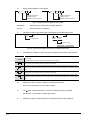
3.2.2
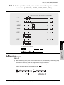
Using word (16 bits) data
Word data is 16-bit numeric data used by basic instructions and application instructions.
The following two types of word data can be used with safety CPU module:
• Decimal constants...................... K-32768 to K32767
• Hexadecimal constants .............. H0000 to HFFFF
Word devices and bit devices designated by digit can be used as word data.
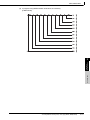
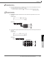
(1) When Using Bit Devices
(a) Bit devices can deal with word data when digits are designated.
Digit designation of bit devices is done by designating " Number of digits
Start number of bit device ".
Digit designation of bit devices can be done in 4-point (4-bit) units, and designation can
be made for K1 to K4.
For example, if X0 is designated for digit designation, the following points would be
designated:
• K1X0 ....... The 4 points X0 to X3 are designated
• K2X0 ....... The 8 points X0 to X7 are designated
• K3X0 ....... The 12 points X0 to XB are designated
• K4X0 ....... The 16 points X0 to XF are designated
XF
XC XB
X8 X7
X4 X3
X0
K1 designation
range
(4 points)
K2 designation range
(8 points)
K3 designation range
(12 points)
K4 designation range
(16 points)
Fig 3.1 Digit Designation Setting Range for 16-Bit Instruction
(b) In cases where digit designation has been made at the source (S), the numeric values
shown in Table 3.1 are those which can be dealt with as source data.
Table 3.1 List of Numeric Values that Can Be Dealt with as Digit Designation
Number of Digits
Designated
3-4
With 16-Bit Instruction
K1 (4 points)
0 to 15
K2 (8 points)
0 to 255
K3 (12 points)
0 to 4095
K4 (16 points)
–32768 to 32767
3.2 Designating Data
3.2.2 Using word (16 bits) data
(c) When destination (D) data is a word device
The word device for the destination becomes 0 following the bit designated by digit
designation at the source.
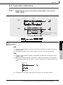
Ladder Example
Processing
16-bit Instruction
K1X0 X3 X2 X1 X0
X010
MOV K1X0
Filled with 0.
D0
b15
D0
Source (S) data
0
b4 b3 b2 b1 b0
0
0
0
0
0
0
0
0
0
0
0 X3 X2 X1 X0
Fig 3.2 Ladder Example and Processing Conducted
Ladder Example
Processing
When source (S) data is a
1
3
2
4
numerical value
H1234
0 0 0 1 0 0 1 0 0 0 1 1 0 1 0 0
X010
MOV H1234
K2M0
M8 M7
M15
K2M0
Destination (D)
Not changed
When source (S) data is a word device
3
b8 b7
b15
D0
M0
0 0 1 1 0 1 0 0
4
b0
1 1 1 0 1 0 1 0 1 0 0 1 1 1 0 1
X10
MOV D0
K2M100
M100
M108 M107
1 0 0 1 1 1 0 1
M115
K2M100
Destination (D)
Not changed
Fig 3.3 Ladder Example and Processing Conducted
(2) Using word devices
Word devices are designated in 1-point (16 bits) units.
M0
MOV
K100
D0
The 1 point D0 (16 bits) is
designated
When digit designation processing is conducted, a random value can be used for
the bit device head device number.
3.2 Designating Data
3.2.2 Using word (16 bits) data
3-5
3
CONFIGURATION
OF INSTRUCTIONS
(d) In cases where digit designation is made at the destination (D), the number of points
designated are used as the destination.
Bit devices below the number of points designated as digits do not change.
3.2.3
Using double word (32 bits) data
Double word data is 32-bit numerical data used by basic instructions and application instructions.
The two types of double word data that can be dealt with by CPU module are as follows:
• Decimal constants...................... K–2147483648 to K2147483647
• Hexadecimal constants .............. H00000000 to HFFFFFFFF
Word devices and bit devices designated by digit designation can be used as double word data.
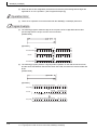
(1) When Using Bit Devices
(a) Digit designation can be used to enable a bit device to deal with double word data.
Digit designation of bit devices is done by designating " Number of digits
Start number of bit device ".
Digit designation of bit devices can be done in 4-point (4-bit) units, and designation can
be made for K1 to K8.
For example, if X0 is designated for digit designation, the following points would be
designated:
• K1X0 .. The 4 points X0 to X3 are
designated
• K2X0 .. The 8 points X0 to X7 are
designated
• K3X0 .. The 12 points X0 to XB are
designated
• K4X0 .. The 16 points X0 to XF are
designated
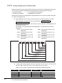
X1F
X1C X1B
X18X17
X14 X13
X10 XF
• K5X0...The 20 points X0 to X13 are
designated
• K6X0...The 24 points X0 to X17 are
designated
• K7X0...The 28 points X0 to X1B are
designated
• K8X0...The 32 points X0 to X1F are
designated
XCXB
X8X7
X4 X3
X0
K1
designation
range
(4 points)
K2 designation range
(8 points)
K3 designation range
(12 points)
K4 designation range
(16 points)
K5 designation range
(20 points)
K6 designation range
(24 points)
K7 designation range
(28 points)
K8 designation range
(32 points)
Fig 3.4 Digit Designation Setting Range for 32-Bit Instructions
(b) In cases where digit designation has been made at the source (S) , the numeric values
shown in Table 3.2 are those which can be dealt with as source data.
Table 3.2 List of Numeric Values that Can Be Dealt with as Digit Designation
Number of Digits
Designated
3-6
With 32 bit Instructions
Number of Digits
Designated
With 32 bit Instructions
K1 (4 points)
0 to 15
K5 (20 points)
0 to 1048575
K2 (8 points)
0 to 255
K6 (24 points)
0 to 16777215
K3 (12 points)
0 to 4095
K7 (28 points)
0 to 268435455
K4 (16 points)
0 to 65535
K8 (32 points)
3.2 Designating Data
3.2.3 Using double word (32 bits) data
2147483648 to 2147483647
(c) When destination (D) data is a word device
The word device for the destination becomes 0 following the bit designated by digit
designation at the source.
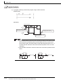
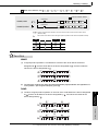
Ladder Example
Processing
32-bit Instruction
K1X0 X3 X2 X1 X0
Filled with 0.
X10
DMOV K1X0
D0
b4 b3 b2 b1 b0
b15
D0 0 0 0 0 0 0 0 0 0 0 0 0 X3 X2 X1 X0
D1 0 0 0 0 0 0 0 0 0 0 0 0 0 0 0 0
Source (S) data
b31
b16
Filled with 0.
(d) In cases where digit designation is made at the destination (D), the number of points
designated are used as the destination.
Bit devices below the number of points designated as digits do not change.
Ladder Example
Processing
When source (S) data is a
H78123456
numerical value
0 0 1 1 0 1 0 0 0 1 0 1 0 1 1 0
3
5
4
6
0 1 1 1 1 0 0 0 0 0 0 1 0 0 1 0
X10
DMOV H78123456 K5M0
7
8
1
2
K5M0
M15
M8 M7
M0
0 0 1 1 0 1 0 0 0 1 0 1 0 1 1 0
Destination (D)
M16
M20 M19
0 0 1 0
M31
Not changed
When the source (S) data is a word device
b15
b8 b7
b0
D0 1 1 1 0 0 1 0 0 0 1 0 1 1 1 0 1
b15
b8 b7
b0
D1 0 0 1 1 0 1 0 0 1 0 0 1 0 1 1 1
X10
DMOV D0
K5M10
Destination (D)
M25
M10
M18 M17
1 1 1 0 0 1 0 0 0 1 0 1 1 1 0 1
M41
M30 M29
M26
0 1 1 1
Not changed
Fig 3.6 Ladder Example and Processing Conducted
When digit designation processing is conducted, a random value can be used for
the bit device head device number.
3.2 Designating Data
3.2.3 Using double word (32 bits) data
3-7
CONFIGURATION
OF INSTRUCTIONS
3
Fig 3.5 Ladder Example and Processing Conducted
(2) Using word devices
A word device designates devices used by the lower 16 bits of data.
A 32-bit instruction uses (designation device number) and (designation device number + 1).
M0
DMOV K100
D0
The 2 points (32 bits) D0 and D1 are designated
32-bit data transfer instruction
3-8
3.2 Designating Data
3.2.3 Using double word (32 bits) data
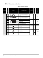
3.3 Subset Processing
Subset processing is used to place limits on bit devices used by basic instructions and
application instructions in order to increase processing speed.
However, the instruction symbol does not change.
To shorten scans, run instructions under the conditions indicated below.
(1) Conditions which each device must meet for subset processing
(a) When using word data
Device
Condition
• Designates a bit device number in a factor of 16
Bit device
3
Word device
• Internal Device
Constants
• No limitations
CONFIGURATION
OF INSTRUCTIONS
• Only K4 can be designated for digit designation.
(b) When using double word data
Device
Condition
• Designates a bit device number in a factor of 16
Bit device
• Only K8 can be designated for digit designation.
Word device
• Internal Device
Constants
• No limitations
(2) Instructions for which subset processing can be used
Types of Instructions
Instruction Symbols
Comparison operation instruction
•
Arithmetic operation
• +,
Data conversion instructions
• BCD, BIN, DBCD, DBIN
Data transfer instruction
Logic operations
,
,
,
,
,
,
,D
, /, INC, DEC, D+, D
,D
,D
,D
,D
,D
,D
, D/, DINC, DDEC
• MOV, DMOV, CML, DCML
• FMOV, BMOV
• WAND, DAND, WOR, DOR, WXOR, DXOR, WXNR, DXNR
3.3 Subset Processing
3-9
3.4 Cautions on Programming (Operation Errors)
Operation errors are returned in the following cases when executing basic instructions,
application instructions and QSCPU dedicated instructions with safety CPU module:
• An error listed on the explanatory page for the individual instruction occurred.
(1) Device range check
Device range checks for the devices used by basic instructions and application instructions
in safety CPU module are as indicated below:
(a) No device range check is made for instructions dealing with fixed-length devices (MOV,
DMOV, etc.).
In cases where the corresponding device range is exceeded, data is written to other
devices.*1
For example, in a case where the data register has been allocated 6 k points, there will
be no error even if it exceeds D6143.
DMOV K100
D6143
D6143 and D6144 are
designated, but since D6144 does not exist,
data in other device will be destroyed.
(b) Device range checks are conducted for instructions dealing with variable-length devices
(BMOV, FMOV, and others which designate transfer numbers).
In cases where the corresponding device range has been exceeded, an operation error
will be returned.
For example, in a case where the data register has been allocated 6 k points, there will
be an error if it exceeds D6143.
BMOV K100 D6143
K2
D6143 and D6144 are
designated but since D6144 does not
an operation error is returned.
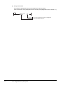
*1: See the figure below for the internal user device assignment order.
SM
Head address
(fixed)
X
Y
M
B
F
SB
V
Contact and coil of T
Contact and coil of ST
Contact and coil of C
Present value of T
Present value of ST
Present value of C
D
W
Empty area
SW
SD
3-10
3.4 Cautions on Programming (Operation Errors)
Remark
Refer to the manual below for how to change the internal user device allocation:
• QSCPU User's Manual (Function Explanation, Program Fundamentals)
(2) Device data check
Device data checks for the devices used by basic instructions and application instructions in
safety CPU module are as indicated below:
(b) When using BCD data
1) Each digit is check for BCD value (0 to 9).
An operation error is returned if individual digits are outside the 0 to 9 (A to F) range.
2) No error is returned even if the operation results in overflow or underflow.
The carry flag does not go on at such times, either.
3.4 Cautions on Programming (Operation Errors)
3-11
3
CONFIGURATION
OF INSTRUCTIONS
(a) When using BIN data
No error is returned even if the operation results in overflow or underflow.
The carry flag does not go on at such times, either.
3.5 Conditions for Execution of Instructions
The following four types of execution conditions exist for the execution of safety CPU module
sequence instructions, basic instructions, application instructions and QSCPU dedicated
instructions:
• Non-conditional execution..... Instructions executed without regard to the ON/OFF status of the
device
Example LD X0, OUT Y10
• Executed at ON..................... Instructions executed while input condition is ON
Example MOV instruction, FMOV instruction
• Executed at leading edge...... Instructions executed only at the leading edge of the input
condition (when it goes from OFF to ON)
Example PLS instruction, MOVP instruction
• Executed at trailing edge....... Instructions executed only at the trailing edge of the input
condition (when it goes from ON to OFF)
Example PLF instruction
For coil or equivalent basic instructions or application instructions, where the same instruction
can be designated for either execution at ON or leading edge execution, a "P" is added after the
instruction name to specify the condition for execution.
• Instruction to be executed at ON
Instruction
• Instruction to be executed at leading edge
Instruction + P
Execution at ON and execution at leading edge for the MOV instruction are designated as follow:
MOV K4X0
D0
Execution during ON
MOVP K4X0
D0
Execution at leading edge
3-12
3.5 Conditions for Execution of Instructions
3.6 Counting Step Number
The number of steps in basic instructions and application instructions of the safety CPU module
may increase depending on the devices to be used.
(1) Counting the number of basic steps
The basic number of steps for basic instructions and application instructions is calculated by
adding the device number and 1.
For example, the "+ instruction" would be calculated as follows:
Number of basic steps: 3
Number of devices 3
Number of basic steps: 4
3
CONFIGURATION
OF INSTRUCTIONS
Number of devices 2
(2) Conditions for increasing the number of steps
In the following case, the number of steps increases over the number of basic steps.
• When a constant is used in device designation with a 32-bit instruction.
Example
Constant (1 step)
Increases 1 step.
32-bit instruction
Constant (1 step)
Constant (1 step)
Increases 2 steps.
32-bit instruction
3.6 Counting Step Number
3-13
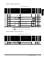
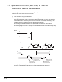
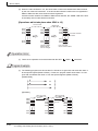
3.7 Operation when OUT, SET/RST, or PLS/PLF
Instructions Use the Same Device
The following describes the operation for executing multiple instructions of OUT, SET/RST, or
PLS/PLF that use the same device in one scan.
(1) OUT instructions using the same device
Do not program more than one OUT instruction using the same device in one scan.
If the OUT instructions using the same device are programmed in one scan, the specified
device will turn ON or OFF every time the OUT instruction is executed, depending on the
operation result of the program up to the relevant OUT instruction.
Since turning ON or OFF of the device is determined when each OUT instruction is
executed, the device may turn ON and OFF repeatedly during one scan.
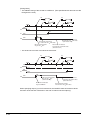
The following diagram shows an example of a circuit that turns the same internal relay (M0)
with inputs X0 and X1 ON and OFF.
[Circuit]
X0
M0
X1
M0
[Timing Chart]
X0
X0
M0
M0
X1
X1
M0
M0
END
END
M0 is turned OFF
because X1 is OFF.
M0 is turned ON
because X1 is ON.
END
ON
X0
OFF
ON
X1
OFF
ON
M0
OFF
M0 is turned ON
because X0 is ON.
M0 remains OFF
because X0 is OFF.
When specifying output (Y) in OUT instruction, the ON/OFF status of the device at the
execution of the last OUT instruction in the scan is returned as the output (Y).
3-14
3.7 Operation when OUT, SET/RST, or PLS/PLF Instructions Use the Same Device
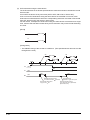
(2) SET/RST instructions using the same device
(a) The SET instruction turns ON the specified device when the execution command is ON
and performs nothing when the execution command is OFF.
For this reason, when SET instructions using the same device are executed two or
more times in one scan, the specified device will be ON if any one of the execution
commands is ON.
(b) The RST instruction turns OFF the specified device when the execution command is
ON and performs nothing when the execution command is OFF.
For this reason, when RST instructions using the same device are executed two or
more times in one scan, the specified device will be OFF if any one of the execution
commands is ON.
[Circuit]
X0
SET M0
X1
RST M0
[Timing Chart]
X0
X0
SET M0
X1
RST M0
END
END
SET M0
X1
RST M0
END
ON
X0
OFF
ON
X1
OFF
M0
OFF
ON
RST M0 is not executed
because X1 is OFF.
(M0 remains ON.)
M0 is turned ON
because X0 is ON.
M0 is turned
OFF because X1 is ON.
SET M0 is not executed
because X0 is OFF.
(M0 remains ON.)
When specifying output (Y) in SET/RST instruction, the ON/OFF status of the device at the
execution of the last instruction in the scan is returned as the output (Y).
3.7 Operation when OUT, SET/RST, or PLS/PLF Instructions Use the Same Device
3-15
3
CONFIGURATION
OF INSTRUCTIONS
(c) When the SET instruction and RST instruction using the same device are programmed
in one scan, the SET instruction turns ON the specified device when the SET execution
command is ON and the RST instruction turns OFF the specified device when the RST
execution command is ON.
When both the SET and RST execution commands are OFF, the ON/OFF status of the
specified device will not be changed.
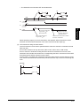
(3) PLS instructions using the same device
The PLS instruction turns ON the specified device when the execution command is turned
ON from OFF.
It turns OFF the device at any other time (OFF to OFF, ON to ON, or ON to OFF).
If two or more PLS instructions using the same device are executed in one scan, each
instruction turns ON the device when the corresponding execution command is turned ON
from OFF and turns OFF the device in other cases.
For this reason, if multiple PLS instructions using the same device are executed in a single
scan, a device that has been turned ON by a PLS instruction may not be turned ON during
one scan.
[Circuit]
X0
PLS M0
X1
PLS M0
[Timing Chart]
• The ON/OFF timing of the X0 and X1 is different. (The specified device does not turn ON
throughout the scan.)
X0
X0
PLS M0
X1
PLS M0
X1
PLS M0
PLS M0
END
END
END
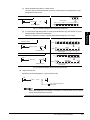
ON
X0
OFF
ON
X1
OFF
ON
M0
ON
OFF
M0 is turned ON
M0 is turned OFF because
because X1 goes OFF ON
X1 is other than OFF ON status.
M0
is
turned
OFF because
M0 is turned ON because
X0 is other than OFF ON status.
X0 goes OFF ON
(M0 remains OFF.)
3-16
3.7 Operation when OUT, SET/RST, or PLS/PLF Instructions Use the Same Device
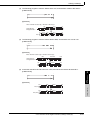
• The X0 and X1 turn ON from OFF at the same time.
X0
X0
PLS M0
X1
PLS M0
END
END
PLS M0
X1
PLS M0
END
ON
X0
OFF
ON
X1
OFF
M0
OFF
ON
3
M0 is turned ON because
X0 goes OFF ON.
M0 is turned OFF
because X1 is other
than OFF ON status.
(M0 remains OFF.)
CONFIGURATION
OF INSTRUCTIONS
M0 is turned ON because
X1 goes OFF ON.
(M0 remains ON.)
M0 is turned OFF because X0 is other
than OFF
ON status.
When specifying output (Y) in PLS instructions, the ON/OFF status of the device at the
execution of the last PLS instruction in the scan is returned as the output (Y).
(4) PLF instructions using the same device
The PLF instruction turns ON the specified device when the execution command is turned
OFF from ON.
It turns OFF the device at any other time (OFF to OFF, OFF to ON, or ON to ON).
If two or more PLF instructions using the same device are executed in one scan, each
instruction turns ON the device when the corresponding execution command is turned OFF
from ON and turns OFF the device in other cases.
For this reason, if multiple PLF instructions using the same device are executed in a single
scan, a device that has been turned ON by a PLF instruction may not be turn ON during one
scan.
[Circuit]
X0
PLF M0
X1
PLF M0
3.7 Operation when OUT, SET/RST, or PLS/PLF Instructions Use the Same Device
3-17
[Timing Chart]
• The ON/OFF timing of the X0 and X1 is different. (The specified device does not turn ON
throughout the scan.)
X0
X0
PLF M0
PLF M0
X1
PLF M0
END
X1
PLF M0
END
END
ON
OFF
X0
ON
X1
OFF
ON
M0 OFF
M0 is turned OFF because X1
is other than ON OFF status.
(M0 remains OFF.)
M0 is turned OFF because
X1 is other than ON OFF status.
M0 is turned ON because
X0 goes ON OFF.
M0 is turned OFF because
X0 is other than ON OFF status.
(M0 remains OFF.)
• The X0 and X1 turn OFF from ON at the same time.
X0
X0
PLF M0
X1
PLF M0
END
END
PLF M0
X1
PLF M0
END
ON
OFF
X0
ON
X1
OFF
ON
M0 OFF
M0 is turned ON because
X1 goes ON OFF.
(M0 remains ON.)
M0 is turned ON because
X0 goes ON OFF.
M0 is turned OFF because X1
is other than ON OFF status.
(M0 remains OFF.)
M0 is turned OFF because
X0 is other than ON OFF status.
When specifying output (Y) in PLF instructions, the ON/OFF status of the device at the
execution of the last PLF instruction in the scan is returned as the output (Y).
3-18
3.7 Operation when OUT, SET/RST, or PLS/PLF Instructions Use the Same Device
APPLICATION
INSTRUCTIONS
BASIC
INSTRUCTIONS
SEQUENCE
INSTRUCTIONS
HOW TO READ
INSTRUCTIONS
CONFIGURATION
OF INSTRUCTIONS
4
GENERAL
DESCRIPTION
HOW TO READ
INSTRUCTIONS
INSTRUCTION TABLES
1
2
3
4
5
6
7
4-1
The description of instructions that are contained in the following chapters are presented in the
following format.
1)
2)
3)
4)
5)
6)
7)
1)
Code used to write instruction (instruction symbol).
2)
Section number and general category of instructions being discussed.
3)
Indicates ladder mode expressions and execution conditions for instructions.
Execution Condition
4)
Non-conditional
Execution
Code recorded on
No symbol
description page
recorded
Executed while ON
Executed One
at ON
Time at OFF
Discusses the data set for each instruction and the data type.
Data Type
4-2
Executed One Time
Meaning
Bit
Bit data or start number of bit device
BIN 16 bits
BIN 16-bit data or start number of word device
BIN 32 bits
BIN 32-bit data or start number of double word device
BCD 4-digit
4-digit BCD data
BCD 8-digit
8-digit BCD data
8)
HOW TO READ
INSTRUCTIONS
4
5)
Devices which can be used by the instruction in question are indicated with circle.
The types of devices that can be used are as indicated below:
Device Type
Internal Devices
(System, User)
Bit
Applicable
devices *1
X, Y, M
SM, F,
B, SB,
Constant *3
Others *3
Word
T, ST, C, *2
D, W, SD,
SW
K, H
N, V
*1: Refer to the manual below for the description for the individual devices.
• QSCPU User's Manual (Function Explanation, Program Fundamentals)
*2: When T, ST and C are used for other than the instructions below, only word data can be used.
(Bit data cannot be used.)
[Instructions that can be used with bit data]
LD, LDI, AND, ANI, OR, ORI, LDP, LDF, ANDP, ANDF, ORP, ORF, OUT, RST
*3: Devices which can be set are described in the "Constant" and the "Others" columns.
6)
Indicates the function of the instruction.
7)
Indicates conditions under which error is returned, and error number.
8)
Indicates simple program examples.
Also indicates the types of individual devices used when the program is executed.
4-3
MEMO
4-4
GENERAL
DESCRIPTION
SEQUENCE
INSTRUCTIONS
INSTRUCTION TABLES
2
CONFIGURATION
OF INSTRUCTIONS
3
4
Ladder block connection, creation of pulses from operation
results, store/read operation results
section
5.1
5.2
Output instruction
Bit device output, output reversal
5.3
Master control instruction
Master control
5.4
Termination instruction
Program termination
5.5
Other instructions
Instructions such as no operation which do not fit in the above
categories
HOW TO READ
INSTRUCTIONS
Connection instructions
Operation start, series connection, parallel connection
Reference
5
SEQUENCE
INSTRUCTIONS
Contact instruction
Processing Details
5.6
6
BASIC
INSTRUCTIONS
Category
7
APPLICATION
INSTRUCTIONS
5
1
5-1
LD, LDI, AND, ANI, OR, ORI
5.1 Contact Instruction
5.1.1
Operation start, series connection, parallel connection
(LD, LDI, AND, ANI, OR, ORI)
LD, LDI, AND, ANI, OR, ORI
Bit device number / Bit designation of word device S
X1/D0.1
LD
X1/D0.1
LDI
X2/D0.2
AND
X2/D0.2
ANI
OR
X3/D0.3
ORI
X3/D0.3
S
: Devices used as contacts (bits)
Set
Data
Internal Devices
Bit
Word
Constants
Others
––
Function
LD, LDI
(1) LD is the A contact operation start instruction, and LDI is the B contact operation start
instruction. They read ON/OFF information from the designated device*1, and use that as
an operation result.
*1: When a bit designation is made for a word device, the device turns ON or OFF depending on the 1/0 status of
the designated bit.
5-2
5.1 Contact Instruction
5.1.1 Operation start, series connection, parallel connection (LD, LDI, AND, ANI, OR, ORI)
LD, LDI, AND, ANI, OR, ORI
AND, ANI
(1) AND is the A contact series connection instruction, and ANI is the B contact series
connection instruction. They read the ON/OFF data of the designated bit device*2, perform
an AND operation on that data and the operation result to that point, and take this value as
the operation result.
*2: When a bit designation is made for a word device, the device turns ON or OFF depending on the 1/0 status of
the designated bit.
(2) There are no restrictions on the use of AND or ANI, but the following applies to the ladder
mode of the GX Developer:
(a) Write.... When AND and ANI are connected in series, a ladder with up to 24 stages can
be displayed.
(b) Read ... When AND and ANI are connected in series, a ladder with up to 24 stages can
be displayed. If the number exceeds 24 stages, up to 24 will be displayed.
OR, ORI
(1) OR is the A contact single parallel connection instruction, and ORI is the B contact single
parallel connection instruction. They read ON/OFF information from the designated
device*3, and perform an OR operation with the operation results to that point, and use the
resulting value as the operation result.
*3: When a bit designation is made for a word device, the device turns ON or OFF depending on the 1/0 status of
the designated bit.
(2) There are no restrictions on the use of OR or ORI, but the following applies to the ladder
mode of the GX Developer
(a) Write.... OR and ORI can be used to create connections of up to 23 ladders.
(b) Read ... OR and ORI can be used to create connections of up to 23 ladders.
The 24th or subsequent ladders cannot be displayed properly.
SEQUENCE
INSTRUCTIONS
5
Remark
LD, LDI, AND, ANI,
OR, ORI
Word device bit designations are made in hexadecimal.
Bit b11 of D0 would be D0.0B.
See 3.2.1 for more information on word device bit designation.
5.1 Contact Instruction
5.1.1 Operation start, series connection, parallel connection (LD, LDI, AND, ANI, OR, ORI)
5-3
LD, LDI, AND, ANI, OR, ORI
Operation Error
(1) There are no operation errors with LD, LDI, AND, ANI, OR, or ORI instructions.
Program Example
(1) A program using LD, AND, OR, and ORI instructions.
[Ladder Mode]
b15
D0
b0
b5
1
0
(2) A program linking contact points established through the use of ANB and ORB instructions.
[Ladder Mode]
b15
D6
b4
b1 b0
1
1
0
0
ORB
ANB
(3) A parallel program with OUT instruction.
[Ladder Mode]
5-4
5.1 Contact Instruction
5.1.1 Operation start, series connection, parallel connection (LD, LDI, AND, ANI, OR, ORI)
LDP, LDF, ANDP, ANDF, ORP, ORF
5.1.2
Pulse operation start, pulse series connection, pulse parallel
connection (LDP, LDF, ANDP, ANDF, ORP, ORF)
LDP, LDF, ANDP, ANDF, ORP, ORF
Bit device number / Bit designation of word device S
X1/D0.1
LDP
X1/D0.1
LDF
X2/D0.2
ANDP
X2/D0.2
ANDF
ORP
X3/D0.3
ORF
5
S
SEQUENCE
INSTRUCTIONS
X3/D0.3
: Devices used as contacts (bits)
Set
Data
Internal Devices
Bit
Constants
Word
Others
LDP, LDF, ANDP, ANDF,
ORP, ORF
––
Function
LDP, LDF
(1) LDP is the leading edge pulse operation start instruction, and is ON only at the leading edge
of the designated bit device (when it goes from OFF to ON). If a word device has been
designated, it is ON only when the designated bit changes from 0 to 1.
In cases where there is only an LDP instruction, it acts identically to instructions for the
creation of a pulse that are executed during ON (
Ladder using an LDP instruction
X0
MOV
K0
D0
X0
P).
Ladder not using an LDP instruction
X0
D0
MOVP
K0
X0
M0
PLS
M0
5.1 Contact Instruction
5.1.2 Pulse operation start, pulse series connection, pulse parallel connection (LDP, LDF, ANDP, ANDF, ORP,
5-5
LDP, LDF, ANDP, ANDF, ORP, ORF
(2) LDF is the trailing edge pulse operation start instruction, and is ON only at the trailing edge
of the designated bit device (when it goes from ON to OFF).
If a word device has been designated, it is ON only when the designated bit changes from 1
to 0.
ANDP, ANDF
(1) ANDP is a leading edge pulse series connection instruction, and ANDF is a trailing edge
pulse series connection instruction. They perform an AND operation with the operation
result to that point, and take the resulting value as the operation result.
The ON/OFF data used by ANDP and ANDF are indicated in the table below:
Device specified in ANDP or ANDF
Bit device
Bit designated for
ANDP State
ANDF State
word device
OFF to ON
0 to 1
OFF
0
ON
1
ON to OFF
1 to 0
ON
OFF
OFF
ON
ORP, ORF
(2) ORP is a leading edge pulse parallel connection instruction, and ORF is a trailing edge pulse
serial connection instruction. They perform an OR operation with the operation result to that
point, and take the resulting value as the operation result.
The ON/OFF data used by ORP and ORF are indicated in the table below:
Device designated in ORP or ORF
Bit device
Bit designated for
ORP State
ORF State
word device
OFF to ON
0 to 1
OFF
0
ON
1
ON to OFF
1 to 0
ON
OFF
OFF
ON
Operation Error
(1) There are no operation errors with LDP, LDF, ANDP, ANDF, ORP, or ORF instructions.
Program Example
(1) The following program executes the MOV instruction at input X0, or at the leading edge of
b10 (bit 11) of data register D0:
[Ladder Mode]
*1: Word device bit designations are performed in hexadecimal.
Bit b10 of D0 would be D0.A.
5-6
5.1 Contact Instruction
5.1.2 Pulse operation start, pulse series connection, pulse parallel connection (LDP, LDF, ANDP, ANDF, ORP,
ANB, ORB
5.2 Connection Instructions
5.2.1
Ladder block series connections and parallel connections
(ANB, ORB)
ANB, ORB
ANB
ANB
Block A
Block B
Block A
ORB
ORB
Block B
Set
Data
Internal Devices
Bit
––
Word
Constants
For parallel connection of 1 contact,
OR or ORI is used.
Others
––
Function
ANB
(1) Performs an AND operation on block A and block B, and takes the resulting value as the
operation result.
SEQUENCE
INSTRUCTIONS
5
(2) The symbol for ANB is not the contact symbol, but rather is the connection symbol.
(1) Conducts an OR operation on Block A and Block B, and takes the resulting value as the
operation result.
(2) ORB is used to perform parallel connections for ladder blocks with two or more contacts.
For ladder blocks with only one contact, use OR or ORI; there is no need for ORB in such
cases.
[Ladder mode]
X1
X0
Y10
0
X2
X3
X4
(3) The ORB symbol is not the contact symbol, but rather is the connection symbol.
5.2 Connection Instructions
5.2.1 Ladder block series connections and parallel connections (ANB, ORB)
5-7
ANB, ORB
ORB
ANB, ORB
Operation Error
(1) There are no operation errors associated with ANB or ORB instructions.
Program Example
(1) A program using ANB and ORB instructions.
[Ladder Mode]
5-8
5.2 Connection Instructions
5.2.1 Ladder block series connections and parallel connections (ANB, ORB)
MPS, MRD, MPP
5.2.2
Operation results push, read, pop (MPS, MRD, MPP)
MPS, MRD, MPP
In the ladder display, MPS, MRD and MPP are not displayed.
Command
Command
MPS
Command
MRD
Command
MPP
Set
Data
––
Internal Devices
Bit
Word
Constants
Others
––
Function
MPS
(1) Stores in memory the operation result (ON or OFF) immediately prior to the MPS instruction.
(2) Up to 16 MPS instructions can be used successively.
MRD
(1) Reads the operation result stored for the MPS instruction, and uses that result to perform the
operation in the next step.
5
SEQUENCE
INSTRUCTIONS
If an MPP instruction is used during this process, the number of uses calculated for the MPS
instruction will be decremented by one.
(1) Reads the operation result stored for the MPS instruction, and uses that result to perform the
operation in the next step.
(2) Clears the operation results stored by the MPS instruction.
(3) Subtracts 1 from the number of MPS instruction times of use.
5.2 Connection Instructions
5.2.2 Operation results push, read, pop (MPS, MRD, MPP)
5-9
MPS, MRD, MPP
MPP
MPS, MRD, MPP
1. The following shows ladders both using and not using the MPS, MRD, and
MPP instructions.
Ladder Using the MPS, MRD and MPP Instruction Ladder not Using MPS, MRD, and MPP Instructions
X0
X1
X0
X2
X1
X2
Y10
X3
Y10
X0
X4
X1
X3
X4
Y11
X5
Y11
X0
X1
X5
Y12
Y12
2. The number of times the MPS and MPP instructions are used must be the
same.
If not, correct ladder display is not possible in the ladder mode of the GX
Developer.
Operation Error
(1) There are no errors associated with the MPS, MRD, or MPP instructions.
Program Example
(1) A program using the MPS, MRD, and MPP instructions.
[Ladder Mode]
5-10
5.2 Connection Instructions
5.2.2 Operation results push, read, pop (MPS, MRD, MPP)
MPS, MRD, MPP
(2) A program using MPS and MPP instructions successively.
[Ladder Mode]
MPS, MRD, MPP
SEQUENCE
INSTRUCTIONS
5
5.2 Connection Instructions
5.2.2 Operation results push, read, pop (MPS, MRD, MPP)
5-11
INV
5.2.3
Operation results inversion (INV)
INV
Command
INV
Internal Devices
Set
Data
Bit
––
Word
Constants
Others
––
Function
(1) Inverts the operation result immediately prior to the INV instruction.
Operation Result Immediately Prior to the Operation Result Following the Execution of
INV Instruction.
the INV Instruction.
OFF
ON
ON
OFF
Operation Error
(1) There are no operation errors associated with the INV instruction.
Program Example
(1) A program which inverts the X0 ON/OFF data, and outputs from Y10.
[Ladder Mode]
[Timing Chart]
ON
X0
Y10
OFF
ON
OFF
5-12
5.2 Connection Instructions
5.2.3 Operation results inversion (INV)
INV
1. The INV instruction operates based on the results of calculation made until the
INV instruction is given. Accordingly, use it in the same position as that of the
AND instruction.
The INV instruction cannot be used at the LD and OR positions.
2. When a ladder block is used, the operation result is inverted within the range of
the ladder block. To operate a ladder using the INV instruction in combination
with the ANB instruction, pay attention to the range that will be inverted.
Range inverted
M0
M1
M2
0
Y10
ANB
M10
M20
END
10
For details of the ANB instruction, refer to Section 5.2.1.
INV
SEQUENCE
INSTRUCTIONS
5
5.2 Connection Instructions
5.2.3 Operation results inversion (INV)
5-13
MEP, MEF
5.2.4
Operation result pulse conversion (MEP, MEF)
MEP, MEF
Command
MEP
Command
MEF
Set
Data
Internal Devices
Bit
Word
––
Constants
Others
––
Function
MEP
(1) If operation results up to MEP instruction are leading edge (from OFF to ON), goes ON
(continuity status).
If operation results up to MEP instruction are anything other than leading edge, goes OFF
(non-continuity status).
(2) Use of the MEP instruction simplifies pulse conversion processing when multiple contacts are
connected in series.
MEF
(1) If operation results up to MEF instruction are trailing edge (from ON to OFF), goes ON
(continuity status).
If operation results up to MEF instruction are anything other than trailing edge, goes OFF
(non-continuity status).
(2) Use of the MEF instruction simplifies pulse conversion processing when multiple contacts are
connected in series.
Operation Error
(1) There are no operation errors associated with the MEP or MEF instructions.
Program Example
(1) A program which performs pulse conversion on the operation results of X0 and X1:
[Ladder Mode]
Because the MEP and MEF instructions operate according to the operation result
immediately before the execution of these instructions, they must be used at the
same position as the AND instruction. The MEP and MEF instructions cannot be
used at the position of LD or OR instruction.
5-14
5.2 Connection Instructions
5.2.4 Operation result pulse conversion (MEP, MEF)
EGP, EGF
5.2.5
Pulse conversion of edge relay operation results (EGP, EGF)
EGP, EGF
EGP
Command
D
Command
D
EGF
D
: Edge relay number where operation results are stored (bits)
Set
Data
D
Internal Devices
Bit
Word
Constants
Others
V
––
Function
EGP
(1) Operation results up to the EGP instruction are stored in memory by the edge relay (V).
(2) Goes ON (continuity status) at the leading edge (OFF to ON) of the operation result up to the
EGP instruction.
(3) The EGP instruction can be used like an AND instruction.
EGF
(1) Operation results up to the EGF instruction are stored in memory by the edge relay (V).
(2) Goes ON at the trailing edge (from ON to OFF) of the operation result up to the EGF
instruction.
5
SEQUENCE
INSTRUCTIONS
If the operation result up to the EGP instruction is other than a leading edge (i.e., from ON to
ON, ON to OFF, or OFF to OFF), it goes OFF (non-continuity status).
If the operation result up to the EGF instruction is other than a trailing edge (i.e., from OFF to
ON, ON to ON, or OFF to OFF), it goes OFF (non-continuity status).
EGP, EGF
(3) The EGF instruction can be used like an AND instruction.
Operation Error
(1) There are no operation errors associated with the EGP or EGF instructions.
5.2 Connection Instructions
5.2.5 Pulse conversion of edge relay operation results (EGP, EGF)
5-15
EGP, EGF
Program Example
(1) A program containing a subroutine program using an EGP instruction
[Ladder Mode]
[Operation]
END processing
X0
ON
OFF
V0 is turned ON because
X0 changes from OFF to ON.
V0
V0 remains OFF because
X0 changes from ON to OFF.
ON
OFF
V0 is turned OFF because
X0 remains ON.
1. Since EGP and EGF instructions are executed according to the results of operation performed immediately before the EGP/EGF instruction, these instructions must be used in the same position as the AND instruction (refer to 5.1.1.).
An EGP and EGF instruction cannot be used at the position of an LD or OR
instruction.
2. EGP and EGF instructions cannot be used at the circuit block positions shown
below.
X0
X1
V0
X0
V0
SET M0
X2
5-16
5.2 Connection Instructions
5.2.5 Pulse conversion of edge relay operation results (EGP, EGF)
X1
SET M0
X2
OUT
5.3 Output Instruction
5.3.1
Out instructions (excluding timers, counters, and annunciators) (OUT)
OUT
Bit device number D
Command
OUT
Y35
Bit designation
of word device D
Command
D0.5
D
: Number of the device to be turned ON and OFF (bits)
Set
Data
D
Internal Devices
Bit
Word
Constants
Others
––
(Except
T, C, F)
Function
5
SEQUENCE
INSTRUCTIONS
(1) Operation results up to the OUT instruction are output to the designated device.
(a) When Using Bit Devices
Operation Results
Coil
OFF
OFF
ON
ON
(b) When Bit Designation has been Made for Word Device
Operation Results
Bit Designated
0
ON
1
OUT
OFF
Operation Error
(1) There are no operation errors associated with OUT instruction.
5.3 Output Instruction
5.3.1 Out instructions (excluding timers, counters, and annunciators) (OUT)
5-17
OUT
Program Example
(1) When Using Bit Devices
[Ladder Mode]
(2) When Bit Designation has been Made for Word Device
[Ladder Mode]
b15
b7 b6 b5
b0
D0
Remark
The number of basic steps is 1 when a device other than a timer, counter and
annunciator is designated for the OUT instruction.
5-18
5.3 Output Instruction
5.3.1 Out instructions (excluding timers, counters, and annunciators) (OUT)
OUT T, OUTH T
5.3.2
Timers (OUT T,OUTH T)
OUT T, OUTH T
K50
Command
T0
Set value
(1 to 32767 is valid)
OUT T
D10
Command
T0
H K50
Command
T0
OUTH T
(High speed timer)
Command
H D10
T0
K50
Command
ST0
OUT ST
(Low speed
retentive timer)
D10
Command
ST0
H K50
Command
ST0
OUTH ST
(High speed
retentive timer)
H D10
Command
ST0
Set value
(Data register value
from 1 to 32767 is valid)
Set value
(Setting in the range from
1 to 32767 is valid)
Set value
(Data register value in the
range from 1 to 32767 is valid)
Set value
(Setting in the range from
1 to 32767 is valid)
Set value
(Data register value in the
range from 1 to 32767 is valid)
Set value
(Setting in the range from
1 to 32767 is valid)
Set value
(Data register value in the
range from 1 to 32767 is valid)
Set
Data
D
Set value
Internal Devices
Bit
(Only T)
––
Word
Constants
K
Others
––
––
––
(Except
T, C)
*1
SEQUENCE
INSTRUCTIONS
D : Timer number (bit)
Set value : Value set for timer (BIN 16 bits)
––
*1: Timer values can be set only in a decimal constant (K). A hexadecimal constant (H) cannot be used for timer
settings.
Function
(1) When the operation results up to the OUT instruction are ON, the timer coil goes ON and the
timer starts measurement; at the time-up (measured value set value), the contact is as
follows:
A Contact
Continuity
B Contact
Non-continuity
5.3 Output Instruction
5.3.2 Timers (OUT T,OUTH T)
5
5-19
OUT T, OUTH T
(Low speed timer)
OUT T, OUTH T
(2) The contact responds as follows when the operation result up to the OUT instruction is a
change from ON to OFF:
Type of Timer
Timer Coil
Low speed timer
Present Value of
Timer
OFF
High speed timer
Prior to Time Up
A Contact
Non-
0
continuity
After Time Up
B Contact
Continuity
A Contact
Noncontinuity
B Contact
Continuity
Low speed
retentive timer
OFF
High speed
Maintains the
Non-
present value
continuity
Continuity
Continuity
Noncontinuity
retentive timer
(3) To clear the present value of a retentive timer and turn the contact OFF after time up, use the
RST instruction.
(4) A negative number ( 32768 to
1) cannot be set as the setting value for the timer.
If the setting value is 0, the timer will time out when the time the OUT instruction is executed.
(5) The following processing is conducted when the OUT instruction is executed:
• OUT T
coil turned ON or OFF
• OUT T
contact turned ON or OFF
• OUT T present value updated
If the same OUT T instruction is executed twice or more times during the same scan, the
present value is updated by the number of times the instruction is executed.
Remark
1. Timer's time limit
Time limit of the timer is set in the PLC system setting of the PLC parameter
dialog box.
QSCPU
Type of Timer
Setting Range
Low speed timer
1 ms to 1000 ms
Low speed retentive timer
(Default: 100 ms)
High speed timer
0.1 ms to 100 ms
High speed retentive timer
(Default: 10 ms)
Setting
unit
1 ms
0.1 ms
2. Refer to the manual below for information on timer counting methods.
• QSCPU User's Manual (Function Explanation, Program Fundamentals)
3. The number of basic steps of the OUT T instruction is 4.
Operation Error
(1) There are no operation errors associated with the OUT T
5-20
5.3 Output Instruction
5.3.2 Timers (OUT T,OUTH T)
instruction.
OUT T, OUTH T
Caution
(1) When creating a program in which the operation of the timer contact triggers the operation of
other timer, create the program according to the operation order of the timers - create the
program for the timer that operates later first.
In the following cases, all timers go ON at the same scan if the program is created in the
order the timers operate.
• If the set value is smaller than a scan time.
• If "1" is set.
Example
• For timers T0 to T2, the program is created in the order the timer operates later.
T1
T0
X0
K1
T2
K1
T1
K1
T0
T2 timer starts measurement from the next scan after turning
T1 contact ON.
T1 timer starts measurement from the next scan after turning
T0 contact ON.
T0 timer starts measurement when X0 is turned ON.
• For timers T0 to T2, the program is created in the order of timer operation.
T0
K1
T1
T1
K1
T2
5
T0 timer starts measurement when X0 is turned ON.
SEQUENCE
INSTRUCTIONS
K1
T0
T1 and T2 timer contacts are turned ON when
T0 contact is turned ON.
OUT T, OUTH T
X0
5.3 Output Instruction
5.3.2 Timers (OUT T,OUTH T)
5-21
OUT T, OUTH T
Program Example
(1) The following program turns Y10 and Y14 ON 10 seconds after X0 has gone ON.
[Ladder Mode]
*2
*2: The set value of the low-speed timer indicates its default time limit (100 ms).
(2) The following program uses the BCD data at X10 to X1F as the timer's set value.
[Ladder Mode]
Converts BCD data at X10 to X1F to BIN
and stores the converted value in D10.
When X2 is turned ON, starts counting using
the data stored in D10 as the set value.
Y15 turns ON at the count up of T2.
(3) The following program turns Y10 ON 250 m after X0 goes ON.
[Ladder Mode]
*3
*3: The set value of the high speed timer indicates its default time limit (10 ms).
5-22
5.3 Output Instruction
5.3.2 Timers (OUT T,OUTH T)
OUT C
5.3.3
Counters (OUT C)
OUT C
K50
Command
C0
OUT C
D10
Command
C1
D :
Set value:
Set
Data
D
Set value
Set value
(1 to 32767 is valid)
Set value
(Data register value from
1 to 32767 is valid)
Counter number (bits)
Counter set value (BIN 16 bits)
Internal Devices
Bit
(Only C)
––
Word
Constants
K
Others
––
––
––
(Except
T, C)
*1
––
*1: Counter values can be set only in a decimal constant (K). A hexadecimal constant (H) cannot be used for the
counter value setting.
Function
A Contact
Continuity
B Contact
Non-continuity
(2) No count is conducted with the operation results at ON. (There is no need to perform pulse
conversion on count input.)
5
SEQUENCE
INSTRUCTIONS
(1) When the operation results up to the OUT instruction change from OFF to ON, 1 is added to
the present value (count value) and the count up status (present value set value), and the
contacts respond as follows:
(3) After the count up status is reached, there is no change in the count value or the contacts until
the RST instruction is executed.
(4) A negative number ( 32768 to
1) cannot be set as the setting value for the timer.
OUT C
If the set value is 0, the processing is identical to that which takes place for 1.
Remark
1. Refer to the manual below for counter counting methods.
• QSCPU User's Manual (Function Explanation, Program Fundamentals)
2. The number of basic steps of the OUT C
instruction is 4.
Operation Error
(1) There are no operation errors associated with the OUT C
instruction.
5.3 Output Instruction
5.3.3 Counters (OUT C)
5-23
OUT C
Program Example
(1) The following program turns Y30 ON after X0 has gone ON 10 times, and resets the counter
when X1 goes ON.
[Ladder Mode]
(2) The following program sets the value for C10 at 10 when X0 goes ON, and at 20 when X1
goes ON.
[Ladder Mode]
Stores 10 in D0 when X0 is turned ON.
Stores 20 in D0 when X1 is turned ON.
C10 counts data stored in D0 as the
set value.
Y30 is turned ON at the count up of C10.
5-24
5.3 Output Instruction
5.3.3 Counters (OUT C)
OUT F
5.3.4
Annunciator output (OUT F)
OUT F
Annunciator number
Command
OUT F
F35
D
: Number of the annunciator to be turned ON (bits)
Set
Data
D
Internal Devices
Bit
(Only F)
Word
Constants
Others
––
Function
(1) Operation results up to the OUT instruction are output to the designated annunciator.
(2) The following responses occur when an annunciator (F) is turned ON.
• The "USER" LED goes ON.
• The annunciator numbers which are ON (F numbers) are stored in special registers
(SD64 to SD79).
• The value of SD63 is incremented by 1.
(4) When the annunciator is turned OFF by the OUT instruction, although the coil goes OFF,
status of the "USER" LED and the contents of SD63 to SD79 are not changed.
To turn OFF the "USER" LED or to delete the annunciator, which was turned OFF by the
OUT F instruction from SD63 to SD79, use the RST F instruction.
5
SEQUENCE
INSTRUCTIONS
(3) If the value of SD63 is 16 (which happens when 16 annunciators are already ON), even if a
new annunciator is turned ON, its number will not be stored at SD64 to SD79.
Operation Error
instruction.
OUT F
(1) There are no operation errors associated with the OUT F
Remark
1. Refer to the manual below for details of annunciators.
• QSCPU User's Manual (Function Explanation, Program Fundamentals)
2. The number of basic steps for the OUT module F
instruction is 2.
5.3 Output Instruction
5.3.4 Annunciator output (OUT F)
5-25
OUT F
Program Example
(1) The following program turns F7 ON when X0 goes ON, and stores the value 7 from SD64 to
SD79.
[Ladder Mode]
[Operation]
X0 ON
5-26
SD63
SD64
SD65
SD66
SD67
0
0
0
0
0
SD79
0
5.3 Output Instruction
5.3.4 Annunciator output (OUT F)
Adds 1.
SD63
SD64
SD65
SD66
SD67
1
7
0
0
0
SD79
0
SET
5.3.5
Setting devices (except for annunciators) (SET)
SET
Command
SET
SET
D
D
: Bit device number to be set (ON)/Word device bit designation (bits)
Set
Data
Internal Devices
Bit
D
Word
(Except
T, C)
Constants
Others
––
Function
(1) When the execution command is turned ON, the status of the designated devices becomes
as shown below:
Device
Device Status
Bit device
Coils and contacts turned ON
When Bit Designation has been Made for Word Device
Designation bit set at 1
(2) Devices turned ON by the instruction remain ON when the same command is turned OFF.
Devices turned ON by the SET instruction can be turned OFF by the RST instruction.
5
SEQUENCE
INSTRUCTIONS
ON
Command
X5
SET
Y10
X5 OFF
ON
X7
RST
Command
Y10
X7 OFF
ON
Y10 OFF
SET
(3) When the execution command is OFF, the status of devices does not change.
5.3 Output Instruction
5.3.5 Setting devices (except for annunciators) (SET)
5-27
SET
Operation Error
(1) There are no operation errors associated with the SET instruction.
Program Example
(1) The following program sets Y8B (ON) when X8 goes ON, and resets Y8B (OFF) when X9
goes ON.
[Ladder Mode]
(2) The following program sets the value of D0 bit 5 (b5) to 1 when X8 goes ON, and set the bit
value to 0 when X9 goes ON.
[Ladder Mode]
Sets b5 of D0 to 1.
Sets b5 of D0 to 0.
b5
b0
D0
Remark
1. The number of basic steps is 1 when a device other than an annunciator is designated for the SET instruction.
2. When using X as a device, use the device numbers that are not used for the
actual input. If the same number is used for the actual input device and input X,
the data of the actual input will be written over the input X specified in the SET
instruction.
5-28
5.3 Output Instruction
5.3.5 Setting devices (except for annunciators) (SET)
RST
5.3.6
Resetting devices (except for annunciators) (RST)
RST
Command
RST
RST
D
D
: Bit device number to be reset/ Word device bit designation (bits)
Word device number to be reset (BIN 16 bits)
Set
Data
Internal Devices
Bit
Word
Constants
Others
––
D
Function
(1) When the execution command is turned ON, the status of the designated devices becomes
as shown below:
Device
Device Status
Turns coils and contacts OFF
Timers and counters
Sets the present value to 0, and turns coils and contacts OFF
When Bit Designation has been Made for Word Device
Sets value of designated bit to 0
Word devices other than timers and counters
Sets contact to 0
5
(2) When the execution command is OFF, the status of devices does not change.
(3) The functions of the word devices designated by the RST instruction are identical to the
following ladder:
X10
Command
Command
X10
RST
D50
MOV
Device number
K0
SEQUENCE
INSTRUCTIONS
Bit device
D50
Device number
RST
Operation Error
(1) There are no operation errors associated with the RST instruction.
Remark
The basic number of steps of the RST instruction is as follows.
a) For bit processing
• Internal device (bit to be specified by bit device or word device): 1
• Timer, counter
:4
b) The number of basic steps is 2 for word processing.
5.3 Output Instruction
5.3.6 Resetting devices (except for annunciators) (RST)
5-29
RST
Program Example
(1) The following program sets the value of the data register to 0.
[Ladder Mode]
Stores the values of X10 to X1F in D8 when
X0 is turned ON.
Sets the value of D8 to 0 when
X5 is turned ON.
(2) The following program resets the 100 ms retentive timer and counter.
[Ladder Mode]
When T225 is set as retentive timer, it is turned ON
when X4 ON time reaches 30 min.
Counts the number of times T225 was turned ON.
Resets the coil, contact and present value of T225
when the contact of T225 is turned ON.
Y55 is turned ON at the count up of C23.
Resets C23 when X5 is turned ON.
5-30
5.3 Output Instruction
5.3.6 Resetting devices (except for annunciators) (RST)
SET F, RST F
5.3.7
Setting and resetting the annunciators (SET F, RST F)
SET F, RST F
Command
SET
SET
D
RST
D
Command
RST
SET
D
: Number of the annunciator to be set (F number) (bits)
RST
D
: Number of the annunciator to be reset (F number) (bits)
Set
Data
D
Internal Devices
Bit
Word
Constants
Others
––
(Only F)
Function
SET
(1) The annunciator designated by
D
is turned ON when the execution command is turned ON.
(2) The following responses occur when an annunciator (F) is turned ON.
• The "USER" LED goes ON.
• The value of SD63 is incremented by 1.
(3) If the value of SD63 is 16 (which happens when 16 annunciators are already ON), even if a
new annunciator is turned ON, its number will not be stored at SD64 to SD79.
RST
D
is turned OFF when the execution command is turned
(2) The annunciator numbers (F numbers) of annunciators that have gone OFF are deleted
from the special registers (SD64 to SD79), and the value of SD63 is decremented by 1.
Remark
1. Refer to the manual below for details of annunciators.
• QSCPU User's Manual (Function Explanation, Program Fundamentals)
2. The number of basic steps for the SET F
and RST F
instructions is 2.
5.3 Output Instruction
5.3.7 Setting and resetting the annunciators (SET F, RST F)
5-31
SET F, RST F
(1) The annunciator designated by
ON.
SEQUENCE
INSTRUCTIONS
5
• The annunciator numbers which are ON (F numbers) are stored in special registers
(SD64 to SD79).
SET F, RST F
(3) When the value of SD63 is "16", the annunciator numbers are deleted from SD64 to SD79
by the use of the RST instruction. If the annunciators whose numbers are not registered in
SD64 to SD79 are ON, these numbers will be registered.
If all annunciator numbers from SD64 to SD79 are turned OFF, the "USER" LED on the front
of the safety CPU module will be turned OFF.
[Operations which take place when SD63 is 16]
Turns F30 ON.
Resets F90.
SD63
SD64
SD65
SD66
16
233
90
700
SD64
SD65
SD66
16
233
90
700
SD64
SD65
SD66
16
233
700
28
SD78
SD79
145
1027
SD78
SD79
145
1027
SD77
SD78
SD79
145
1027
30
Values of SD63,
SD64 to SD79
are not changed.
F number for SD67
is stored.
F30, which was
ON, is stored in SD79.
Operation Error
(1) There are no operation errors associated with the SET F
or RST F
instructions.
Program Example
(1) The following program turns annunciator F11 ON when X1 goes ON, and stores the value 11
at the special register (SD64 to SD79). Further, the program resets annunciator F11 if X2
goes ON, and deletes the value 11 from the special registers (SD64 to SD79).
[Ladder Mode]
[Operation]
When X1 is ON
5-32
SD63
SD64
SD65
SD66
0
0
0
0
SD78
SD79
0
0
Adds 1
When X2 is ON
SD63
SD64
SD65
SD66
SD67
1
11
0
0
0
SD78
SD79
0
0
5.3 Output Instruction
5.3.7 Setting and resetting the annunciators (SET F, RST F)
Subtracts 1
SD63
SD64
SD65
SD66
SD67
0
0
0
0
0
SD78
SD79
0
0
PLS, PLF
5.3.8
Leading edge and trailing edge output (PLS, PLF)
PLS, PLF
Command
PLS
PLS
D
PLF
D
Command
PLF
D
: Pulse conversion device (bits)
Internal Devices
Set
Data
Bit
Word
Constants
Others
––
D
Function
PLS
(1) Turns ON the designated device when the execution command is turned OFF
turns OFF the device in any other case the execution command is turned OFF
ON ON, ON OFF or OFF OFF of the execution command).
ON, and
ON (i.e., at
ON
X5 OFF
X5
PLS
ON
M0
5
SEQUENCE
INSTRUCTIONS
When there is one PLS instruction for the device designated by D during one scan, the
specified device turns ON one scan.
See 3.7 for the operation to be performed when the PLS instruction for the same device is
executed more than once during one scan.
M0 OFF
1 scan
(2) If the RUN/STOP/RESET switch is changed from RUN to STOP after the execution of the
PLS instruction, the PLS instruction will not be executed again even if the switch is set back
to RUN.
X0
PLS
M0
Changes the RUN/STOP/
Changes the RUN/STOP/
RESET switch of CPU module
RESET switch of CPU
Changes the RUN/STOP/
from STOP to RUN.
module from STOP to RUN.
RESET switch of CPU
Changes the RUN/STOP/
module from RUN to STOP.
RESET switch of CPU
LD X0
LD X0
LD X0
module from RUN to STOP.
PLS M0
END 0
ON
X0 OFF
PLS M0
END
PLS M0
END
CPU operation
stop time
0
CPU operation
stop time
ON
M0 OFF
1 scan of PLS M0
5.3 Output Instruction
5.3.8 Leading edge and trailing edge output (PLS, PLF)
5-33
PLS, PLF
1 scan
PLS, PLF
(3) When designating a latch relay (L) for the execution command and turning the power supply
OFF to ON with the latch relay ON, the execution command turns OFF to ON at the first
scan, executing the PLS instruction and turning ON the designated device.
The device turned ON at the first scan after power-ON turns OFF at the next PLS instruction.
PLF
(1) Turns ON the designated device when the execution command is turned ON
turns OFF the device in any other case the execution command is turned ON
OFF OFF, OFF ON or ON ON of the execution command).
OFF, and
OFF (i.e., at
When there is one PLF instruction for the device designated by D during one scan, the
specified device turns ON one scan.
See 3.7 for the operation to be performed when the PLF instruction for the same device is
executed more than once during one scan.
ON
X5 OFF
X5
PLF
ON
M0
M0 OFF
1 scan 1 scan
(2) If the RUN/STOP/RESET switch is changed from RUN to STOP after the execution of the
PLF instruction, the PLF instruction will not be executed again even if the switch is set back
to RUN.
Operation Error
(1) There are no operation errors associated with the PLS or PLF instructions.
Program Example
(1) The following program executes the PLS instruction when X9 goes ON.
[Ladder Mode]
[Timing Chart]
ON
X9 OFF
ON
M9 OFF
5-34
1 scan
5.3 Output Instruction
5.3.8 Leading edge and trailing edge output (PLS, PLF)
PLS, PLF
(2) The following program executes the PLF instruction when X9 goes OFF.
[Ladder Mode]
[Timing Chart]
ON
X9 OFF
ON
M9 OFF
1 scan
PLS, PLF
SEQUENCE
INSTRUCTIONS
5
5.3 Output Instruction
5.3.8 Leading edge and trailing edge output (PLS, PLF)
5-35
FF
5.3.9
Bit device output reverse (FF)
FF
Command
FF
FF
D
D
: Device number of the device to be reversed (bits)
Internal Devices
Set
Data
Bit
Word
Constants
Others
––
D
Function
(1) Reverses the output status of the device designated by
turned OFF ON.
D
when the execution command is
Device Status
Device
Prior to FF execution
Bit device
Bit designated for word device
After FF execution
OFF
ON
ON
OFF
0
1
1
0
Operation Error
(1) There are no operation errors associated with the FF instruction.
Program Example
(1) The following program reverses the output of Y10 when X9 goes ON.
[Ladder Mode]
[Timing Chart]
ON
X9
OFF
ON
Y10
5-36
OFF
5.3 Output Instruction
5.3.9 Bit device output reverse (FF)
FF
(2) The following program reverses b10 (bit 10) of D10 when X0 goes ON.
[Ladder Mode]
[Timing Chart]
ON
0
1
0
5
SEQUENCE
INSTRUCTIONS
b10 of D10
OFF
FF
X0
5.3 Output Instruction
5.3.9 Bit device output reverse (FF)
5-37
MC, MCR
5.4 Master Control Instructions
5.4.1
Setting and resetting the master control (MC, MCR)
MC, MCR
Command
MC
n
MC
n
D
D
Master control ladder
MCR
MCR
n
: Nesting (N0 to N14) (Nesting)
D
: Number of the device to turn ON (bits)
Set
Data
Internal Devices
n
––
Bit
Word
Constants
n
Others
N
––
––
D
––
Function
(3) The master control instruction is used to enable the creation of highly efficient ladder
switching sequence programs, through the opening and closing of a common bus for
ladders.
A ladder using the master control would look as shown below:
Ladder of actual operation
Ladder displayed in the GX Developer ladder mode
X0
N1
X0
MC
M0
X1 X3 M7
N1
M0
N1
MC
M0
X1 X3 M7
N1
Y47
M5
M0
Y47
Executed only
when X0 is ON
M5
Y4F
X6 X4
Y4F
X6 X4
MCR
MCR
N1
X0F
N1
XF
Y10
Y40
Remark
Inputting contacts on the vertical bus is not necessary when programming in the
write mode of the GX Developer.
These will be automatically displayed when the "conversion" operation is conducted
after the creation of the ladder and then "read" mode is set.
5-38
5.4 Master Control Instructions
5.4.1 Setting and resetting the master control (MC, MCR)
MC, MCR
MC
(1) If the execution command of the MC instruction is ON when master control is commenced,
the result of the operation from the MC instruction to the MCR instruction will be exactly as
the instruction (ladder) shows.
If the execution command of the MC instruction is OFF, the result of the operation from the
MC instruction to the MCR instruction will be as shown below:
Device
Device Status
High speed timer
Count value goes to 0, coils and contacts all go OFF
Low speed timer
High speed retentive timer
Coils go OFF, but counter values and contacts all maintain
Low speed retentive timer
current status.
Counter
Devices in OUT instruction
All turned OFF
SET, RST
Basic,
Devices in the following instructions:
Maintain current status
Application
(2) Even when the MC instruction is OFF, instructions from the MC instruction to the MCR
instruction will be executed, so scan time will not be shortened.
(3) By changing the device designated by
number as often as desired.
(4) Coils from devices designated by
D
D
, the MC instruction can use the same nesting (N)
are turned ON when the MC instruction is ON.
Further, using these same devices with the OUT instruction or other instructions will cause
them to become double coils, so devices designated by
instructions.
D
should not be used within other
SEQUENCE
INSTRUCTIONS
MCR
5
(1) This is the instruction for recovery from the master control, and indicates the end of the
master control range of operation.
(2) Do not place contact instructions before the MCR instruction.
However, when the MCR instructions are nested in one place, all master controls can be
terminated with the lowest nesting (N) number.
(Refer to the "Cautions when Using Nesting Architecture" in the program example.)
Operation Error
(1) There are no operation errors associated with the MC or MCR instructions.
5.4 Master Control Instructions
5.4.1 Setting and resetting the master control (MC, MCR)
5-39
MC, MCR
(3) Use the MC instruction and MCR instruction of the same nesting number as a set.
MC, MCR
Program Example
(1) The master control instruction can be used in nesting. The different master control regions
are distinguished by nesting (N). Nesting can be performed from N0 to N14.
The use of nesting enables the creation of ladders which successively limit the execution
condition of the program.
A ladder using nesting would appear as shown below:
Ladderdisplayed in the GX Developer
ladder mode
[Ladder of actual operation]
A
A
MC N0 M15
N0
MC N0 M15
N0
M15
M15
Executed when A
is ON
B
B
MC N1 M16
N1
M16
MC N1 M16
N1
C
M16
C
MC N2 M17
N2
Executed when A
and B are ON
M17
MC N2 M17
N2
M17
MCR N2
Executed when A, B
and C are ON
MCR N2
Executed when A
and B are ON
MCR N1
MCR N1
Executed when
A is ON
MCR N0
MCR N0
Not related to A, B
and C
5-40
5.4 Master Control Instructions
5.4.1 Setting and resetting the master control (MC, MCR)
MC, MCR
Cautions when Using Nesting Architecture
(1) Nesting can be used up to 15 times (N0 to N14)
When using nesting, nests should be inserted from the lower to higher nesting number (N)
with the MC instruction, and from the higher to the lower order with the MCR instruction.
If this order is reversed, there will be no nesting architecture, and the safety CPU module will
not be capable of performing correct operations.
For example, if nesting is designated in the order N1 to N0 by the MC instruction, and also
designated in the N1 to N0 order by the MCR instruction, the vertical bus will intersect and a
correct master control ladder will not be produced.
Ladder displayed in the GX Developer
ladder mode
A
N1
[Ladder of actual operation]
A
MC N1 M15
M15
N1
MC N1 M15
M15
B
MC N0 M16
MC N0 M16
N0
M16
M16
MCR N1
MCR N0
MCR N0
(2) If the nesting architecture results in MCR instructions concentrated in one location, all
master controls can be terminated by use of just the lowest nesting number (N).
X1
X1
MC N0 M15
N0
M15
MC N0 M15
N0
X2
M15
X2
MC N1 M16
N1
MC N1 M16
N1
M16
X3
M16
X3
MC N2 M17
N2
5
SEQUENCE
INSTRUCTIONS
MCR N1
MC N2 M17
N2
M17
M17
MCR N2
MCR N0
MCR N1
MCR N0
5.4 Master Control Instructions
5.4.1 Setting and resetting the master control (MC, MCR)
5-41
MC, MCR
N0
END
5.5 Termination Instruction
5.5.1
End sequence program (END)
END
END
END
Set
Data
Internal Devices
Bit
––
Constants
Word
Others
––
Function
(1) The termination of a sequence program is indicated.
Execution of the END instruction will cause the safety CPU module to terminate the program
that was being executed.
0
Sequence program
END
(2) END instruction is automatically set by the GX Developer during programming.
Operation Error
(1) There are no operation errors associated with the END instruction.
5-42
5.5 Termination Instruction
5.5.1 End sequence program (END)
NOP, NOPLF, PAGE n
5.6 Other Instructions
5.6.1
No-operation (NOP, NOPLF, PAGE n)
NOP, NOPLF, PAGE n
In the ladder display, NOP is not displayed.
Command
NOP
NOP
NOPLF
NOPLF
PAGE n
PAGE n
Set
Data
Internal Devices
n
––
Bit
Word
Constants
K
Others
––
Function
NOP
NOPLF
(1) This is a no operation instruction that has no impact on any operations up to that point.
(2) NOPLF instruction is used to make a page break at a desired position when printing out from
the GX Developer.
• A page break will be inserted between ladder blocks with the presence of the NOPLF
instruction.
• The ladder cannot be displayed correctly if an NOPLF instruction is inserted in the midst
of a ladder block.
Do not insert an NOPLF instruction in the midst of a ladder block.
(3) For the print out operation by the GX Developer, refer to the GX Developer Operating
Manual.
PAGE n
(1) This is a no operation instruction that has no impact on any operations up to that point.
(2) No processing is performed at the GX Developer with this instruction.
5.6 Other Instructions
5.6.1 No-operation (NOP, NOPLF, PAGE n)
5-43
NOP, NOPLF, PAGE n
(2) NOP instruction is used to insert space for debugging a sequence program.
SEQUENCE
INSTRUCTIONS
5
(1) This is a no operation instruction that has no impact on any operations up to that point.
NOP, NOPLF, PAGE n
Operation Error
(1) There are no errors associated with the NOP, NOPLF, or PAGE instructions.
Program Example
NOP
(1) Contact closed......... Deletes AND or ANI instruction.
[Ladder Mode]
Before change
Changing to NOP
After change
(2) Contact closed......... LD, LDI changed to NOP (Note carefully that changing the LD and
LDI instructions to NOP completely changes the nature of the ladder.)
[Ladder Mode]
Before change
Changing to NOP
After change
5-44
5.6 Other Instructions
5.6.1 No-operation (NOP, NOPLF, PAGE n)
NOP, NOPLF, PAGE n
[Ladder Mode]
Before change
Changing to LD T3
Changing to NOP
After change
NOPLF
[Ladder Mode]
NOP, NOPLF, PAGE n
SEQUENCE
INSTRUCTIONS
5
5.6 Other Instructions
5.6.1 No-operation (NOP, NOPLF, PAGE n)
5-45
NOP, NOPLF, PAGE n
• Printing the ladder will result in the following:
0
X0
MOV
K1
D30
MOV
K2
D40
5
NOPLF
-1X1
6
Y40
8
END
PAGE n
[Ladder Mode]
NOP
5-46
5.6 Other Instructions
5.6.1 No-operation (NOP, NOPLF, PAGE n)
A page break will be inserted between
ladder blocks with the presence
of NOPLF instruction.
GENERAL
DESCRIPTION
BASIC
INSTRUCTIONS
INSTRUCTION TABLES
2
CONFIGURATION
OF INSTRUCTIONS
3
4
Arithmetic operation instruction
Compares data to data
Adds, subtracts, multiplies, divides, increments, or
decrements data with other data
HOW TO READ
INSTRUCTIONS
instruction
section
6.1
6.2
Data conversion instructions
Converts data types
6.3
Data transfer instruction
Transmits designated data
6.4
5
SEQUENCE
INSTRUCTIONS
Comparison operation
Processing Details
6
BASIC
INSTRUCTIONS
Category
Reference
7
APPLICATION
INSTRUCTIONS
6
1
6-1
=, <>, >, <=, <, >=
6.1 Comparison Operation Instruction
6.1.1
BIN 16-bit data comparisons (= , <> , >, <= , <, >=)
=, <>, >, <=, <, >=
indicates "= / < > / > / <= / < / >=".
LD
S1
S2
S1
S2
S1
S2
Command
AND
Command
Command
OR
S1
,
S2
: Data for comparison or start number of the devices where the data for comparison is stored (BIN 16 bits)
Internal Devices
Set
Data
Bit
Word
Constants
K, H
Others
S1
––
S2
––
Function
(1) Treats BIN 16-bit data from device designated by
designated by
S2
S1
and BIN 16-bit data from device
as an a normally-open contact, and performs comparison operation.
(2) The results of the comparison operations for the individual instructions are as follows:
Instruction
Symbol in
Condition
=
S2
<>
S1
>
S1
<=
S1
<
S1
>=
S1
=
>
<
Comparison
Operation Result
Instruction
Symbol in
Condition
S1
=
S1
S2
<>
S2
>
S1
S2
<=
S1
S2
<
S1
S2
>=
S1
S2
Comparison
Operation Result
S2
=
S1
S2
Continuity
Non-continuity
>
S2
S2
<
S2
(3) When S1 and S2 are assigned by a hexadecimal constant and the numerical value (8 to F)
whose most significant bit (b15) is "1" is designated as a constant, the value is considered
as a negative BIN value in comparison operation.
6-2
6.1 Comparison Operation Instruction
6.1.1 BIN 16-bit data comparisons (= , <> , >, <= , <, >=)
=, <>, >, <=, <, >=
Operation Error
(1) There are no operation errors associated with the
,
,
,
,
or
instructions.
Program Example
(1) The following program compares the data at X0 to XF with the data at D3, and turns Y33 ON
if the data is identical.
[Ladder Mode]
(2) The following program compares BIN value K100 to the data at D3, and establishes
continuity if the data in D3 is something other than 100.
[Ladder Mode]
(3) The following program compares the BIN value 100 with the data in X0 to XF, and
establishes continuity if the D3 data is less than 100.
[Ladder Mode]
6
BASIC
INSTRUCTIONS
(4) The following program compares the data in D0 and D3, and if the data in D0 is equal to or
less than the data in D3, establishes continuity.
=, <>, >, <=, <, >=
[Ladder Mode]
6.1 Comparison Operation Instruction
6.1.1 BIN 16-bit data comparisons (= , <> , >, <= , <, >=)
6-3
D=, D< >, D>, D<=, D<, D>=
6.1.2
BIN 32-bit data comparisons (D=, D<>, D>, D<=, D<, D>=)
D=, D< >, D>, D<=, D<, D>=
indicates "D= / D< > / D> / D<= / D< / D>=".
LD
S1
S2
S1
S2
S1
S2
Command
AND
Command
Command
OR
S1
,
S2
: Data for comparison or start number of the devices where the data for comparison is stored (BIN 32 bits)
Internal Devices
Set
Data
Bit
Word
Constants
K, H
Others
S1
––
S2
––
Function
(1) Treats BIN 32-bit data from device designated by
designated by
S2
S1
and BIN 32-bit data from device
as an a normally-open contact, and performs comparison operation.
(2) The results of the comparison operations for the individual instructions are as follows:
Instruction
Symbol in
Condition
D=
S2
D <>
S1
D>
S1
D <=
S1
D<
S1
D >=
S1
=
>
<
Comparison
Operation Result
Instruction
Symbol in
Condition
S1
D=
S1
S2
D <>
S2
D>
S1
S2
D <=
S1
S2
D<
S1
S2
D >=
S1
S2
Comparison
Operation Result
S2
=
S1
S2
Continuity
Non-continuity
>
S2
S2
<
S2
(3) When S1 and S2 are assigned by a hexadecimal constant and the numerical value (8 to F)
whose most significant bit (b31) is "1" is designated as a constant, the value is considered
as a negative BIN value in comparison operation.
(4) Data used for comparison should be designated by a 32-bit instruction (DMOV instruction,
etc.).
If designation is made with a 16-bit instruction (MOV instruction, etc.), comparisons of large
and small values cannot be performed correctly.
6-4
6.1 Comparison Operation Instruction
6.1.2 BIN 32-bit data comparisons (D=, D<>, D>, D<=, D<, D>=)
D=, D< >, D>, D<=, D<, D>=
Operation Error
(1) There are no operation errors associated with the D , D
instruction.
,D ,D
,D
or D
Program Example
(1) The following program compares the data at X0 to X1F with the data at D3 and D4, and
turns Y33 ON, if the data at X0 to X1F and the data at D3 and D4 match.
[Ladder Mode]
(2) The following program compares BIN value K38000 to the data at D3, and D4, and
establishes continuity if the data in D3 and D4 is something other than 38000.
[Ladder Mode]
(3) The following program compares BIN value K 80000 to the data at D3 and D4, and
establishes continuity if the data in D3 and D4 is less than 80000.
[Ladder Mode]
(4) The following program compares the data in D0 and D1 with the data in D3 and D4, and
establishes continuity if the data in D0 and D1 is equal to or less than the data in D3 and D4.
BASIC
INSTRUCTIONS
6
D=, D< >, D>, D<=, D<,
D>=
[Ladder Mode]
6.1 Comparison Operation Instruction
6.1.2 BIN 32-bit data comparisons (D=, D<>, D>, D<=, D<, D>=)
6-5
+(P), -(P)
6.2 Arithmetic Operation Instructions
6.2.1
BIN 16-bit addition and subtraction operations (+(P), –(P))
+(P), -(P)
When two data are set (
D
+
D
S
,
D
–
D
S
)
indicates "+ / -".
Command
+,
S
D
S
D
Command
+P,
P
P
S
: Data for additing/subtracting or start number of the devices where the data for additing/subtracting is stored
(BIN 16 bits)
S1
D
:Start number of the devices where the data to be added to/subtracted from is stored (BIN 16 bits)
Internal Devices
Set
Data
Bit
Constants
K, H
Word
Others
––
––
D
––
Function
+
(1) Adds 16-bit BIN data designated by
D
to 16-bit BIN data designated by
result of the addition at the device designated by
D
b15
b0
S
and
D
b15
+
and stores the
.
S
5678 (BIN)
(2) Values for
D
S
D
b0
b15
1234 (BIN)
can be designated between
b0
6912 (BIN)
32768 and 32767 (BIN, 16 bits).
(3) The judgment of whether data is positive or negative is made by the most significant bit
(b15).
• 0: Positive
• 1: Negative
(4) The following will happen when an underflow or overflow is generated in an operation result:
The carry flag in this case does not go ON.
. K32767
(H7FFF)
+K2
(H0002)
. K 32768 +K 2
( H 8000) ( H FFFE)
6-6
K 32767
(H8001)
Since b15 is "1", the judgment is
a negative value.
K32766
(H7FFE)
Since b15 is "0", the judgment is
a positive value.
6.2 Arithmetic Operation Instructions
6.2.1 BIN 16-bit addition and subtraction operations (+(P), –(P))
+(P), -(P)
–
(1) Subtracts 16-bit BIN data designated by
D
from 16-bit BIN data designated by
stores the result of the subtraction at the device designated by
D
b15
S
b0
5678 (BIN)
(2) Values for
S
and
D
b15
D
S
and
.
D
b0
b15
1234 (BIN)
can be designated between
b0
4444 (BIN)
32768 and 32767 (BIN, 16 bits).
(3) The judgment of whether data is positive or negative is made by the most significant bit
(b15).
• 0: Positive
• 1: Negative
(4) The following will happen when an underflow or overflow is generated in an operation result:
The carry flag in this case does not go ON.
. K 32768
(H8000)
K2
(H0002)
K32766
(H7FFE)
Since b15 is "0", the judgment is
a positive value.
. K32767
(H7FFF)
K 2
(HFFFE)
K 32767
(H8001)
Since b15 is "1", the judgment is
a negative value.
Operation Error
(1) There are no operation errors associated with the +(P) or –(P) instructions.
+(P), -(P)
BASIC
INSTRUCTIONS
6
6.2 Arithmetic Operation Instructions
6.2.1 BIN 16-bit addition and subtraction operations (+(P), –(P))
6-7
+(P), -(P)
When three data are set ( S1 +
S2
D
,
–
S1
S2
D
)
indicates "+ / -".
Command
+,
S1
S2
D
S1
S2
D
Command
+P,
P
P
S1
:
Data to be added to/subtracted from or start number of the devices where the data to be added to/
subtracted from is stored (BIN 16 bits)
S2
:
Data for additing/subtracting or start number of the devices where the data for additing/subtracting is stored
(BIN 16 bits)
D
:
Start number of the devices where the addition/subtraction operation result will be stored (BIN 16 bits)
Internal Devices
Set
Data
Bit
Constants
K, H
Word
Others
S1
––
S2
––
––
D
––
Function
+
(1) Adds 16-bit BIN data designated by
S1
to 16-bit BIN data designated by
result of the addition at the device designated by
S1
b0
5678 (BIN)
S1
,
S2
and
D
b15
+
and stores the
.
D
S2
b15
(2) Values for
D
S2
b0
b15
1234 (BIN)
can be designated between
b0
6912 (BIN)
32768 and 32767 (BIN, 16 bits).
(3) The judgment of whether data is positive or negative is made by the most significant bit
(b15).
• 0: Positive
• 1: Negative
(4) The following will happen when an underflow or overflow is generated in an operation result:
The carry flag in this case does not go ON.
. K32767
(H7FFF)
+K2
(H0002)
. K 32768 +K 2
(H8000)
( H FFFE)
6-8
K 32767
(H8001)
Since b15 is "1", the judgment is
a negative value.
K32766
(H7FFE)
Since b15 is "0", the judgment is
a positive value.
6.2 Arithmetic Operation Instructions
6.2.1 BIN 16-bit addition and subtraction operations (+(P), –(P))
+(P), -(P)
–
(1) Subtracts 16-bit BIN data designated by
S1
from 16-bit BIN data designated by
stores the result of the subtraction at the device designated by
S1
b0
5678 (BIN)
(2) Values for
S1
,
S2
and
D
b15
and
.
D
S2
b15
D
S2
b0
1234 (BIN)
can be designated between
b15
b0
4444 (BIN)
32768 and 32767 (BIN, 16 bits).
(3) The judgment of whether data is positive or negative is made by the most significant bit
(b15).
• 0: Positive
• 1: Negative
(4) The following will happen when an underflow or overflow is generated in an operation result:
The carry flag in this case does not go ON.
. K 32768
(H8000)
K2
(H0002)
K32766
(H7FFE)
Since b15 is "0", the judgment is
a positive value.
. K32767
(H7FFF)
K 2
(HFFFE)
K 32767
(H8001)
Since b15 is "1", the judgment is
a negative value.
Operation Error
(1) There are no operation errors associated with the +(P) or –(P) instructions.
Program Example
(1) The following program adds, when X5 is turned ON, the data at D3 and D0 and outputs the
operation result at Y38 to Y3F.
[Ladder Mode]
BASIC
INSTRUCTIONS
6
(2) The following program outputs the difference between the set value for timer T3 and its
present value in BCD to Y40 to Y53.
+(P), -(P)
[Ladder Mode]
6.2 Arithmetic Operation Instructions
6.2.1 BIN 16-bit addition and subtraction operations (+(P), –(P))
6-9
D+(P), D-(P)
6.2.2
BIN 32-bit addition and subtraction operations (D+(P), D–(P))
D+(P), D-(P)
When two data are set ((
(
D
+1,
D
)–(
+ 1,
S
S
D
+ 1,
)
(
D
)+(
+1,
D
D
S
+ 1,
S
)
(
+ 1,
D
D
),
))
indicates "D+ / D-".
Command
D+, D
S
D
S
D
Command
D+P, D P
P
S
: Data for additing/subtracting or start number of the devices where the data for additing/subtracting is stored
(BIN 32 bits)
D
: Start number of the devices where the data to be added to/subtracted from is stored (BIN 32 bits)
Internal Devices
Set
Data
Bit
Constants
K, H
Word
Others
––
S
––
D
––
Function
D+
(1) Adds 32-bit BIN data designated by
D
to 32-bit BIN data designated by
result of the addition at the device designated by
D +1
b31 b16 b15 b0
567890 (BIN)
(2) The values for
(BIN 32 bits).
S
and
S +1
D
D
+
D
, and stores the
.
S
b31 b16 b15 b0
123456 (BIN)
S
D +1
D
b31 b16 b15 b0
691346 (BIN)
can be designated at between
2147483648 and 2147483647
(3) Judgment of whether the data is positive or negative is made on the basis of the most
significant bit (b31).
• 0: Positive
• 1: Negative
(4) The following will happen when an underflow or overflow is generated in an operation result:
The carry flag in this case does not go ON.
. K 2147483647
( H7FFFFFFF)
+K2
K 2147483647
( H00000002) ( H80000001 )
. K 214748364 8 +K 2
K 214748364 6
( H8000000 0)
(HFFFFFFFE) ( H7FFFFFFE)
6-10
Since b31 is "1", the judgment is
a negative value.
Since b31 value is "0", the judgment is
a positive value.
6.2 Arithmetic Operation Instructions
6.2.2 BIN 32-bit addition and subtraction operations (D+(P), D–(P))
D+(P), D-(P)
D–
(1) Subtracts 32-bit BIN data designated by
D
from 32-bit BIN data designated by
stores the result of the subtraction at the device designated by
D +1
S +1
D
b31 b16 b15 b0
567890 (BIN)
(2) The values for
(BIN 32 bits).
S
and
D
S
b31 b16 b15 b0
123456 (BIN)
D +1
D
S
and
.
D
b31 b16 b15 b0
444434 (BIN)
can be designated at between
2147483648 and 2147483647
(3) Judgment of whether the data is positive or negative is made on the basis of the most
significant bit (b31).
• 0: Positive
• 1: Negative
(4) The following will happen when an underflow or overflow is generated in an operation result:
The carry flag in this case does not go ON.
. K 214748364 8
(H80000000)
K2
( H00000002)
. K 2147483647
( H7FFFFFFF)
K 2147483647
K 2
( HFFFFFFFE) (H80000001 )
K214748364 6
(H7FFFFFFE)
Since b31 is "0", the judgment is
a positive value.
Since b31 is "1", the judgment is
a negative value.
Operation Error
(1) There are no operation errors associated with the +(P) or –(P) instructions.
D+(P), D-(P)
BASIC
INSTRUCTIONS
6
6.2 Arithmetic Operation Instructions
6.2.2 BIN 32-bit addition and subtraction operations (D+(P), D–(P))
6-11
D+(P), D-(P)
When three data are set (( S1 + 1,
( S1 + 1,
S1
) – ( S2 + 1,
S2
)
(
D
S1
) + ( S2 + 1,
+1,
D
S2
)
(
D
+ 1,
D
),
))
indicates "D+ / D-".
Command
D+,D
S1
S2
D
S1
S2
D
Command
D+P, D P
P
S1
: Data to be added to/subtracted from or start number of the devices where the data to be added to/subtracted
from is stored (BIN 32 bits)
S2
: Data for additing/subtracting or start number of the devices where the data for additing/subtracting is stored
(BIN 32 bits)
D
: Start number of the devices where the addition/subtraction operation result will be stored (BIN 32 bits)
Internal Devices
Set
Data
Bit
Constants
K, H
Word
Others
S1
––
S2
S1
––
––
D
––
Function
D+
(1) Adds 32-bit BIN data designated by
S1
to 32-bit BIN data designated by
result of the addition at the device designated by
S1
+1
S2
S1
b31 b16 b15 b0
567890 (BIN)
(2) The values for
(BIN 32 bits).
S1
,
S2
and
D
+
+1
S2
b31 b16 b15 b0
123456 (BIN)
D
S2
, and stores the
.
D +1
D
b31 b16 b15 b0
691346 (BIN)
can be designated at between
2147483648 and 2147483647
(3) Judgment of whether the data is positive or negative is made on the basis of the most
significant bit (b31).
• 0: Positive
• 1: Negative
(4) The following will happen when an underflow or overflow is generated in an operation result:
The carry flag in this case does not go ON.
. K2147483647
(H7FFFFFFF)
+K2
(H00000002)
. K 214748364 8 +K 2
(H80000000)
(HFFFFFFFE)
6-12
K 2147483647
(H80000001)
Since b31 is "1", the judgment is
a negative value.
K2147483646
(H7FFFFFFE)
Since b31 is "0", the judgment is
a positive value.
6.2 Arithmetic Operation Instructions
6.2.2 BIN 32-bit addition and subtraction operations (D+(P), D–(P))
D+(P), D-(P)
D–
(1) Subtracts 32-bit BIN data designated by
S1
from 32-bit BIN data designated by
stores the result of the subtraction at the device designated by
S1
+1
S1
S2
b31 b16 b15 b0
567890 (BIN)
(2) The values for
(BIN 32 bits).
S1
,
S2
and
D
+1
S2
b31 b16 b15 b0
123456 (BIN)
D +1
D
S2
and
.
D
b31 b16 b15 b0
444434 (BIN)
can be designated at between
2147483648 and 2147483647
(3) Judgment of whether the data is positive or negative is made on the basis of the most
significant bit (b31).
• 0: Positive
• 1: Negative
(4) The following will happen when an underflow or overflow is generated in an operation result:
The carry flag in this case does not go ON.
. K 214748364 8
(H80000000 )
K2
(H00000002)
. K2147483647
(H7FFFFFFF)
K 214748364 7
K 2
(HFFFFFFFE) (H80000001)
K214748364 6
(H7FFFFFFE)
Since b31 is "0", the judgment is
a positive value.
Since b31 is "1", the judgment is
a negative value.
Operation Error
(1) There are no operation errors associated with the +(P) or –(P) instructions.
Program Example
6
BASIC
INSTRUCTIONS
(1) The following program adds 28-bit data from X10 to X2B to the data at D9 and D10 when X0
goes ON, and outputs the result of the operation to Y30 to Y4B.
[Ladder Mode]
D+(P), D-(P)
(2) The following program subtracts the data from M0 to M23 from the data at D0 and D1 when
XB goes ON, and stores the result at D10 and D11.
[Ladder Mode]
6.2 Arithmetic Operation Instructions
6.2.2 BIN 32-bit addition and subtraction operations (D+(P), D–(P))
6-13
*(P), /(P)
6.2.3
BIN 16-bit multiplication and division operations (*(P), /(P))
*(P), /(P)
indicates " , /".
Command
*
/
S1
S2
D
S1
S2
D
Command
* P, / P
P
S1
: Data to be multiplied/divided or start number of the devices where the data to be multiplied/divided is stored
(BIN 16 bits)
S2
: Data for multiplying/dividing or start number of the devices where the data for multiplying/dividing is stored
(BIN 16 bits)
D
: Start number of the devices where the multiplication/division operation result will be stored (BIN 32 bits)
Internal Devices
Set
Data
Bit
Constants
K, H
Word
Others
S1
––
S2
––
––
D
––
Function
*
(1) Multiplies BIN 16-bit data designated by
S1
and BIN 16-bit data designated by
stores the result in the device designated by
b15
b0
D
D +1
b15
5678 (BIN)
b0
D
b31 b16 b15 b0
7006652 (BIN)
1234 (BIN)
is a bit device, designation is made from the lower bits.
Example
(3) Values for
K1........ Lower 4 bits (b0 to b3)
K4........ Lower 16 bits (b0 to b15)
K8........ 32 bits (b0 to b31)
S1
and
S2
(4) Judgments whether
can be designated between
S1
,
S2
, and
most significant bit (b15 for
S1
D
, and
32768 and 32767 (BIN, 16 bits).
are positive or negative are made on the basis of the
S2
, for
D
and b31).
• 0: Positive
• 1: Negative
6-14
, and
.
S2
S1
(2) If
D
S2
6.2 Arithmetic Operation Instructions
6.2.3 BIN 16-bit multiplication and division operations (*(P), /(P))
*(P), /(P)
/
(1) Divides BIN 16-bit data designated by
the result in the device designated by
D
S1
S2
b15
b0
5678 (BIN)
and BIN 16-bit data designated by
S1
S2
, and stores
.
b15
b0
1234 (BIN)
Quotient
Remainder
D
D +1
b15
b0 b15
b0
742 (BIN)
4 (BIN)
(2) If a word device has been used, the result of the division operation is stored as 32 bits, and
both the quotient and remainder are stored; if a bit device has been used, 16 bits are used
and only the quotient is stored.
Quotient:
Remainder:
(3) Values for
S1
Stored at the lower 16 bits
Stored at the upper 16 bits (Stored only when using a word device)
and
S2
can be designated between
32768 and 32767 (BIN, 16 bits).
(4) Judgment whether values for S1 , S2 , D and D + 1 are positive or negative is made on the
basis of the most significant bit (b15). (Sign is attached to both the quotient and remainder.)
• 0: Positive
• 1: Negative
Operation Error
(1) In any of the following cases, an operation error occurs, the error flag (SM0) turns ON, and
the corresponding error code is stored into SD0.
• Attempt to divide
S2
by 0.
(Error code: 4100)
Program Example
(1) The following program divides "5678" by "1234" when X5 goes ON, and stores the result at
D3 and D4.
(2) The following program divides BIN data at X8 to XF by BIN data at X10 to X1B, and outputs
the result of the division operation to Y30 to Y3F.
BASIC
INSTRUCTIONS
6
[Ladder Mode]
(3) The following program divides, when X3 is turned ON, the data at X8 to XF by 3.14 and
outputs the operation result at Y30 to Y3F.
[Ladder Mode]
6.2 Arithmetic Operation Instructions
6.2.3 BIN 16-bit multiplication and division operations (*(P), /(P))
6-15
*(P), /(P)
[Ladder Mode]
D*(P), D/(P)
6.2.4
BIN 32-bit multiplication and division operations (D*(P), D/(P))
D*(P), D/(P)
indicates "D , D/".
Command
D*, D/
S1
S2
D
S1
S2
D
Command
D* P, D/ P
P
S1
: Data to be multiplied/divided or start number of the devices where the data to be multiplied/divided is stored
(BIN 32 bits)
S2
: Data for multiplying/dividing or start number of the devices where the data for multiplying/dividing is stored
(BIN 32 bits)
D
: Start number of the devices where the multiplication/division operation result will be stored (BIN 64 bits)
Internal Devices
Set
Data
Bit
Constants
K, H
Word
Others
S1
––
S2
––
––
D
––
Function
D*
(1) Multiplies BIN 32-bit data designated by
S1
and BIN 32-bit data designated by
stores the result in the device designated by
S1 +1
S2 +1
S1
b31 b16 b15 b0
567890 (BIN)
D
b31 b16 b15 b0
123456 (BIN)
, and
.
D +3
S2
S2
D +2
D +1
D
b63 b48 b47 b32 b31 b16 b15
70109427840 (BIN)
b0
(2) If D is a bit device, only the lower 32 bits of the multiplication result will be considered, and
the upper 32 bits cannot be designated.
Example
K1........ Lower 4 bits (b0 to b3)
K4........ Lower 16 bits (b0 to b15)
K8........ Lower 32 bits (b0 to b31)
If the upper 32 bits of the bit device are required for the result of the multiplication operation,
first temporarily store the data in a word device, then transfer the word device data to the bit
device by designating (
(3) The values for
(BIN 32 bits).
S1
and
(4) Judgments whether
S1
S2
,
+ 2) and (
D
D
+ 3) data.
can be designated at between
S2
, and
most significant bit (b31 for
S1
D
and
are positive or negative are made on the basis of the
S2
, b63 for
D
).
• 0: Positive
• 1: Negative
6-16
2147483648 and 2147483647
6.2 Arithmetic Operation Instructions
6.2.4 BIN 32-bit multiplication and division operations (D*(P), D/(P))
D*(P), D/(P)
D/
(1) Divides BIN 32-bit data designated by
the result in the device designated by
S1 +1
S2 +1
S1
b31 b16 b15 b0
567890 (BIN)
and BIN 32-bit data designated by
S1
D
S2
, and stores
.
D +1
S2
b31 b16 b15 b0
123456 (BIN)
D
b31 b16 b15
4 (BIN)
D +3
D +2
b0 b31 b16 b15 b0
74066 (BIN)
(2) With a word device, the division operation result is stored in 64 bits and both the quotient
and remainder are stored. With a bit device, only the quotient is stored as the operation
result in 32 bits.
Quotient:
Remainder:
(3) The values for
(BIN 32 bits).
Stored at the lower 32 bits
Stored at the upper 32 bits (Stored only when using a word device)
S1
and
S2
can be designated at between
(4) Judgment whether values for S1 , S2 ,
basis of the most significant bit (b31).
D
and
D
2147483648 and 2147483647
+ 2 are positive or negative is made on the
(Sign is attached to both the quotient and remainder)
• 0: Positive
• 1: Negative
Operation Error
(1) In any of the following cases, an operation error occurs, the error flag (SM0) turns ON, and
the corresponding error code is stored into SD0.
• Attempt to divide
S2
by 0.
(Error code: 4100)
Program Example
6
BASIC
INSTRUCTIONS
(1) The following program divides the BIN data at D7 and D8 by the BIN data at D18 and D19
when X5 is ON, and stores the result at D1 to D4.
[Ladder Mode]
D*(P), D/(P)
(2) The following program outputs the value resulting when the data at X8 to XF is multiplied by
3.14 to Y30 to Y3F when X3 is ON.
[Ladder Mode]
6.2 Arithmetic Operation Instructions
6.2.4 BIN 32-bit multiplication and division operations (D*(P), D/(P))
6-17
INC(P), DEC(P)
6.2.5
Incrementing and decrementing 16-bit BIN data
(INC(P), DEC(P))
INC(P), DEC(P)
indicates "INC / DEC".
Command
INC, DEC
D
Command
P
INCP, DECP
D
: Start number of devices for INC (+1)/DEC (
Set
Data
Internal Devices
Bit
1) operation (BIN 16 bits)
Constants
Word
D
Others
––
D
Function
INC
(1) Adds 1 to the device designated by
D
(16-bit data).
D
b15
D
b0
b15
+1
5678 (BIN)
b0
5679 (BIN)
(2) When INC/INCP operation is executed for the device designated by
32767, the value
32768 is stored at the device designated by
D
D
, whose content is
.
DEC
(1) Subtracts 1 from the device designated by
D
(16-bit data).
D
b15
D
b0
5678 (BIN)
b15
1
b0
5677 (BIN)
(2) When DEC/DECP operation is executed for the device designated by
32768, the value 32767 is stored at the device designated by
D
D
, whose content is
.
Operation Error
(1) There are no operation errors associated with the INC(P)/DEC(P) instruction.
6-18
6.2 Arithmetic Operation Instructions
6.2.5 Incrementing and decrementing 16-bit BIN data (INC(P), DEC(P))
INC(P), DEC(P)
Program Example
(1) The following program outputs the present value at the counter C0 to C20 to the area Y30 to
Y3F in BCD, every time X8 is turned ON. (When present value is less than 9999)
[Ladder Mode]
Outputs the present value of C (D+Z1) to Y30 to Y3F.
Executes Z1+1.
Sets 0 to Z1 when Z1=21 or X7 (reset input).
(2) The following is a down counter program.
[Ladder Mode]
Transfers 100 to D8 when X7 is turned ON.
Turns X8 from OFF to ON
when M38 is OFF, which executes "D8 - 1".
M38 is turned ON when "D8=0".
INC(P), DEC(P)
BASIC
INSTRUCTIONS
6
6.2 Arithmetic Operation Instructions
6.2.5 Incrementing and decrementing 16-bit BIN data (INC(P), DEC(P))
6-19
DINC(P), DDEC(P)
6.2.6
Incrementing and decrementing 32-bit BIN data
(DINC(P), DDEC(P))
DINC(P), DDEC(P)
indicates "DINC / DDEC".
Command
DINC, DDEC
D
Command
P
DINCP, DDECP
D
D
: Start number of devices for DINC(+1) or DDEC(–1) operation (BIN 32 bits)
Internal Devices
Set
Data
Bit
Constants
Word
Others
––
D
Function
DINC
(1) Adds 1 to the device designated by
D +1
D
(32-bit data).
D
D +1
b31 b16 b15 b0
73500 (BIN)
+1
D
b31 b16 b15 b0
73501 (BIN)
(2) When DINC/DINCP operation is executed for the device designated by
2147483647, the value
D
, whose content is
2147483648 is stored at the device designated by
D
.
DDEC
(1) Subtracts 1 from the device designated by
D +1
D
b31 b16 b15 b0
73500 (BIN)
D
(32-bit data).
D +1
1
D
b31 b16 b15 b0
73499 (BIN)
(2) When DDEC/DDECP operation is executed for the device designated by
is 0, the value
1 is stored at the device designated by
D
.
Operation Error
(1) There are no operation errors associated with DINC(P) or DDEC(P).
6-20
6.2 Arithmetic Operation Instructions
6.2.6 Incrementing and decrementing 32-bit BIN data (DINC(P), DDEC(P))
D
, whose content
DINC(P), DDEC(P)
Program Example
(1) The following program adds 1 to the data at D0 and D1 when X0 is ON.
[Ladder Mode]
(2) The following program adds 1 to the data set at X10 to X27 when X0 goes ON, and stores
the result at D3 and D4.
[Ladder Mode]
(3) The following program subtracts 1 from the data at D0 and D1 when X0 goes ON.
[Ladder Mode]
(4) The following program subtracts 1 from the data set at X10 to X27 when X0 goes ON, and
stores the result at D3 and D4.
[Ladder Mode]
DINC(P), DDEC(P)
BASIC
INSTRUCTIONS
6
6.2 Arithmetic Operation Instructions
6.2.6 Incrementing and decrementing 32-bit BIN data (DINC(P), DDEC(P))
6-21
BCD(P), DBCD(P)
6.3 Data Conversion Instructions
6.3.1
Conversion from BIN data to 4-digit and 8-digit BCD
(BCD(P), DBCD(P))
BCD(P), DBCD(P)
BCD(P), DBCD(P)
indicates "BCD / DBCD".
Command
BCD, DBCD
S
D
S
D
Command
BCDP, DBCDP
P
: BIN data or start number of the devices where the BIN data is stored (BIN 16/32 bits)
D : Start number of the devices where BCD data will be stored (BCD 4/8 digits)
Internal Devices
Set
Data
Bit
Constants
K, H
Word
Others
––
––
D
––
Function
BCD
(1) Converts BIN data (0 to 9999) at the device designated by
the device designated by
D
.
−32768 16384 8192 4096 2048 1024 512 256
S
BIN 9999
0
0
1
0
0
1
1
128
64
32
16
8
4
2
1
0
0
0
0
1
1
1
1
1
Always filled with 0.
8000 4000 2000 1000 800 400
D
BCD 9999
1
0
0
to BCD data, and stores it at
1
0
1
Thousands digit
BCD conversion
200 100
0
1
80
40
20
10
8
4
2
1
1
0
0
1
1
0
0
1
Hundreds digit
Tens digit
Ones digit
DBCD
(1) Converts BIN data (0 to 99999999) at the device designated by
it at the device designated by
D
to BCD data, and stores
.
S (Lower 16 digits)
231
230
229
228
227
226
225
224
223
222
221
220
219
218
217
216
215
214
213
212
211
210
29
28
27
26
25
24
23
22
21
20
S +1 (Upper 16 digits)
0 0 0 0 0 1 0 1 1 1 1 1 0 1 0 1 1 1 1 0 0 0 0 0 1 1 1 1 1 1 1 1
10 0
10 1
10 2
10 4
10 5
10 6
BCD conversion
8
4
2
1
8
4
2
1
8
4
2
1
8
4
2
1
8
4
2
1
8
4
2
1
8
4
2
1
8
4
2
1
10 7
Always filled with 0 (Upper 5 digits)
10 3
S BIN 99999999
D BCD 99999999 1 0 0 1 1 0 0 1 1 0 0 1 1 0 0 1 1 0 0 1 1 0 0 1 1 0 0 1 1 0 0 1
Ten millions Millions
digit
digit
Hundred Ten thousands Thousands Hundreds
digit
digit
thousands digit
digit
D +1 (Upper 4 digits)
6-22
Tens
digit
D (Lower 4 digits)
6.3 Data Conversion Instructions
6.3.1 Conversion from BIN data to 4-digit and 8-digit BCD (BCD(P), DBCD(P))
Ones
digit
BCD(P), DBCD(P)
Operation Error
(1) In any of the following cases, an operation error occurs, the error flag (SM0) turns ON, and
the corresponding error code is stored into SD0.
• The data of
is other than 0 to 9999 at BCD instruction.
• The data of
or
(Error code: 4100)
+1 is other thean 0 to 99999999 at DBCD instruction.
(Error code: 4100)
Program Example
(1) The following program outputs the present value of C4 from Y20 to Y2F to the BCD display
device.
Output
power
supply
0 1 0 1
0 1 1 0
0 1 1 1
Y23
Y22
Y21
Y20
8
4
2
1
Y27
Y26
Y25
Y24
80
40
20
10
Y2B
Y2A
Y29
Y28
800
400
200
100
8000
4000
2000
1000
COM
Y2F
Y2E
Y2D
Y2C
PLC output module
1 0 0 0
7-segment indicator
[Ladder Mode]
(2) The following program outputs 32-bit data from D0 to D1 to Y40 to Y67.
PLC output module
Y67-Y64
Y63-Y60
Y5F-Y5C
Y5B-Y58
Y57-Y54
Y53-Y50
Y4F-Y4C
Y4B-Y48
Y47-Y44
Y43-Y40
BCD(P), DBCD(P)
Output
power
supply
7-segment indicator
[Ladder Mode]
6.3 Data Conversion Instructions
6.3.1 Conversion from BIN data to 4-digit and 8-digit BCD (BCD(P), DBCD(P))
BASIC
INSTRUCTIONS
6
6-23
BIN(P), DBIN(P)
6.3.2
Conversion from BCD 4-digit and 8-digit data to BIN data
(BIN(P), DBIN(P))
BIN(P), DBIN(P)
indicates "BIN / DBIN".
Command
BIN, DBIN
S
D
S
D
Command
BINP, DBINP
P
: BCD data or start number of the devices where the BCD data is stored (BCD 4/8 digits)
D : Start number of the devices where BIN data will be stored (BIN 16/32 bits)
Internal Devices
Set
Data
Bit
Constants
K, H
Word
Others
––
––
D
––
Function
BIN
(1) Converts BCD data (0 to 9999) at device designated by
device designated by
D
.
8000 4000 2000 1000 800 400 200 100
S
BCD 9999
1
to BIN data, and stores at the
0
0
1
1
Thousands digit
0
0
1
80
40
20
10
8
4
2
1
1
0
0
1
1
0
0
1
Hundreds digit
Tens digit
Ones digit
BIN conversion
32768 16384 8192 4096 2048 1024 512 256 128
D
BIN 9999
0
0
0
1
0
1
1
1
0
64
32
16
8
4
2
1
0
0
0
1
1
1
1
Always filled with 0.
DBIN
(1) Converts BCD data (0 to 99999999) at device designated by
.
102
103
104
105
106
S
8
4
2
1
8
4
2
1
8
4
2
1
8
4
2
1
8
4
2
1
8
4
2
1
8
4
2
1
8
4
2
1
107
S +1
100
D
101
the device designated by
to BIN data, and stores at
S BCD 99999999 1 0 0 1 1 0 0 1 1 0 0 1 1 0 0 1 1 0 0 1 1 0 0 1 1 0 0 1 1 0 0 1
Ten millions Millions
digit
digit
Tens
digit
Hundred
Ten thousands Thousands Hundreds
thousands digit
digit
digit
digit
BIN conversion
D
2 31
2 30
2 29
2 28
2 27
2 26
2 25
2 24
2 23
2 22
2 21
2 20
2 19
2 18
2 17
2 16
2 15
2 14
2 13
2 12
2 11
2 10
29
28
27
26
25
24
23
22
21
20
D +1
Ones
digit
D BIN 99999999
0 0 0 0 0 1 0 1 1 1 1 1 0 1 0 1 1 1 1 0 0 0 0 0 1 1 1 1 1 1 1 1
Always filled with 0.
6-24
6.3 Data Conversion Instructions
6.3.2 Conversion from BCD 4-digit and 8-digit data to BIN data (BIN(P), DBIN(P))
BIN(P), DBIN(P)
Operation Error
(1) In the following cases, an operation error occurs, the error flag (SM0) turns ON, an error
code is stored in SD0, and the instruction is not executed.
• When values other than 0 to 9 are designated to any digits of
.(Error code: 4100)
In this regard, however, the error above can be suppressed by turning SM722 ON.
However, the instruction is not executed regardless of whether SM722 is turned ON or OFF
if the designated value is out of the available range.
For the BINP/DBINP instruction, the next operation will not be performed until the command
(execution condition) is turned from OFF to ON regardless of the presence/absence of an
error.
Program Example
(1) The following program converts the BCD data at X10 to X1B to BIN when X8 is ON, and stores it
at D8.
COM
COM
8
4
2
1
0
X13
1
X12
1
X11
0
X10
COM
80
40
20
10
0
X17
0
X16
1
X15
1
X14
X1F
X1E
X1D
X1C
COM
Input
power
supply
0
X1B
0
X1A
1
X19
0
X18
Can be used in
other purposes
800
400
200
100
BCD digital switch
PLC input module
[Ladder Mode]
BIN(P), DBIN(P)
BASIC
INSTRUCTIONS
6
6.3 Data Conversion Instructions
6.3.2 Conversion from BCD 4-digit and 8-digit data to BIN data (BIN(P), DBIN(P))
6-25
BIN(P), DBIN(P)
(2) The following program converts the BCD data at X10 to X37 to BIN when X8 is ON, and
stores it at D0 and D1.
(Addition of the BIN data converted from BCD at X20 to X37 and the BIN data converted
from BCD at X10 to X1F)
BCD digital switch
Input power supply
X37-X34
X33-X30
X2F-X2C
X2B-X28
X27-X24
X23-X20
X1F-X1C
X1B-X18
X17-X14
X13-X10
PLC output module
[Ladder Mode]
If the data set at X10 to X37 is a BCD value which exceeds 2147483647, the value at D0
and D1 will be a negative value, because it exceeds the range of numerical values that can
be handled by a 32-bit device.
6-26
6.3 Data Conversion Instructions
6.3.2 Conversion from BCD 4-digit and 8-digit data to BIN data (BIN(P), DBIN(P))
NEG(P), DNEG(P)
6.3.3
Complement of 2 of BIN 16- and 32-bit data (sign reversal)
(NEG(P), DNEG(P))
NEG(P), DNEG(P)
indicates "NEG / DNEG".
Command
NEG, DNEG
D
Command
NEGP, DNEGP
P
D
D : Start number of the devices where the data for which complement of 2 is performed is stored (BIN 16/32 bits)
Internal Devices
Set
Data
Bit
Constants
Word
Others
––
D
Function
NEG
(1) Reverses the sign of the 16-bit device designated by
by
D
and stores at the device designated
D
.
16 bits
Sign
conversion
After
D
execution
1
1
0
1
0
1
0
1
0
1
0
1
0
1
b0
0
0
0
0
0
0
0
0
0
0
0
0
0
0
0
0
0
1
0
1
0
1
0
1
0
1
0
1
0
1
0
1
0
b15
0 1
0
1
0
1
0
1
0
1
0
1
0
1
1
b0
0
21846
6
BASIC
INSTRUCTIONS
b15
1 0
Before
D
execution
21846
NEG(P), DNEG(P)
(2) Used when reversing positive and negative signs.
6.3 Data Conversion Instructions
6.3.3 Complement of 2 of BIN 16- and 32-bit data (sign reversal) (NEG(P), DNEG(P))
6-27
NEG(P), DNEG(P)
DNEG
(1) Reverses the sign of the 32-bit device designated by
by
D
D
and stores at the device designated
.
32 bits
b31
1 1
Before
D
execution
Sign
conversion
After
D
execution
1
1
1
1
1
1
0
1
0
0
1
0
b0
0
0
0
0
0
0
0
0
0
0
0
0
0
0
0
1
1
1
1
1
1
1
0
1
0
0
1
0
0
b31
0 0
0
0
0
0
0
1
0
1
1
1
0
b0
0
−218460
218460
(2) Used when reversing positive and negative signs.
Operation Error
(1) There are no operation errors associated with the NEG(P) or DNEG(P) instructions.
Program Example
(1) The following program calculates a total for the data at D10 through D20 when XA goes ON,
and seeks an absolute value if the result is negative.
[Ladder Mode]
M3 is turned ON when D10
Executes "D10
D20.
D20".
Calculates the absolute value
(complement of 2) when M3 is ON.
6-28
6.3 Data Conversion Instructions
6.3.3 Complement of 2 of BIN 16- and 32-bit data (sign reversal) (NEG(P), DNEG(P))
MOV(P), DMOV(P)
6.4 Data Transfer Instructions
6.4.1
16-bit and 32-bit data transfers (MOV(P), DMOV(P))
MOV(P), DMOV(P)
indicates "MOV / DMOV".
Command
MOV, DMOV
S
D
S
D
Command
P
MOVP, DMOVP
S
: Data to be transferred or the number of the device where the data to be transferred is stored (BIN 16/32 bits)
D
: Number of the device where the data will be transferred (BIN 16/32 bits)
Internal Devices
Set
Data
Bit
Constants
K, H
Word
Others
––
––
D
––
Function
MOV
(1) Transfers the 16-bit data from the device designated by
Before
transfer
S
b15
1 0
D
b15
1 0
1
1
0
1
0
0
0
1
1
1
0
S
to the device designated by
D
.
b0
0
0
1
0
b0
1 0
6
1
1
0
1
0
0
0
1
1
1
0
BASIC
INSTRUCTIONS
Transfer
After
transfer
DMOV
(1) Transfers 32-bit data at the device designated by
Before
S
transfer
b15
1 0
1
1
b15
1 0
1
1
D
.
S
0
1
0
b0 b15
0 0 1
1
Transfer
D +1
After
D
transfer
to the device designated by
0
1
0
b0 b15
0 0 1
1
1
0
0
1
b0
0
0
0
1
b0
0
MOV(P), DMOV(P)
S +1
S
D
1
Operation Error
(1) There are no operation errors associated with the MOV(P) or DMOV(P) instructions.
6.4 Data Transfer Instructions
6.4.1 16-bit and 32-bit data transfers (MOV(P), DMOV(P))
6-29
MOV(P), DMOV(P)
Program Example
(1) The following program stores input data from X0 to XB at D8.
[Ladder Mode]
(2) The following program stores the constant K155 at D8 when X8 goes ON.
[Ladder Mode]
009BH
b15
b8 b7
b0
D8 0 0 0 0 0 0 0 0 1 0 0 1 1 0 1 1
(3) The following program stores the data from D0 and D1 at D7 and D8.
[Ladder Mode]
(4) The following program stores the data from X0 to X1F at D0 and D1.
[Ladder Mode]
6-30
6.4 Data Transfer Instructions
6.4.1 16-bit and 32-bit data transfers (MOV(P), DMOV(P))
CML(P), DCML(P)
6.4.2
16-bit and 32-bit negation transfers (CML(P), DCML(P))
CML(P), DCML(P)
indicates "CML / DCML".
Command
CML, DCML
S
D
S
D
Command
P
CMLP, DCMLP
S
: Data to be reversed or the number of the device where data to be reversed is stored (BIN 16/32 bits)
D
: Number of the device where the reversing result will be stored (BIN 16/32 bits)
Internal Devices
Set
Data
Bit
Constants
K, H
Word
Others
––
––
D
––
Function
CML
(1) Inverts 16-bit data designated by
designated by
Before
S
execution
After
D
execution
D
bit by bit, and transfers the result to the device
S
.
b15
1 0
b15
0 1
1
1
0
1
0
0
0
1
1
1
0
0
1
b0
0
0
1
1
0
b0
1
Inversion
0
0
1
0
1
1
1
0
0
6
(1) Inverts 32-bit data designated by
D
bit by bit, and transfers the result to the device
S
.
S +1
Before
S
execution
b15
1 0
1
S
0
1
1
After
D
execution
0
0
b0 b15
0 0 1
1
Inversion
D +1
b15
0 1
0
1
0
b0 b15
1 1 1 0
0
1
0
0
1
b0
0
1
1
0
b0
1
CML(P), DCML(P)
designated by
BASIC
INSTRUCTIONS
DCML
D
0
Operation Error
(1) There are no operation errors associated with the CML(P) or DCML(P) instructions.
6.4 Data Transfer Instructions
6.4.2 16-bit and 32-bit negation transfers (CML(P), DCML(P))
6-31
CML(P), DCML(P)
Program Example
(1) The following program inverts the data from X0 to X7, and transfers result to D0.
[Ladder Mode]
[Operation]
When "Number of bits of (S) < Number of bits of (D)"
X7
These bits are
all regarded as 0.
X0
11010000
b8 b7
b15
b0
D0 1 1 1 1 1 1 1 1 0 0 1 0 1 1 1 1
(2) The following program inverts the data at M16 to M23, and transfers the result to Y40 to
Y47.
[Ladder Mode]
[Operation]
When "Number of bits of (S) < Number of bits of (D)"
M23
These bits are
all regarded as 0
M16
01011100
Y4B Y48 Y47
Y40
111110100011
(3) The following program inverts the data at D0 when X3 is ON, and stores the result at D16.
[Ladder Mode]
[Operation]
D0
b15
b8 b7
b0
1101100110101111
b15
b8 b7
b0
D16 0 0 1 0 0 1 1 0 0 1 0 1 0 0 0 0
6-32
6.4 Data Transfer Instructions
6.4.2 16-bit and 32-bit negation transfers (CML(P), DCML(P))
CML(P), DCML(P)
(4) The following program inverts the data at X0 to X1F, and transfers results to D0 and D1.
[Ladder Mode]
[Operation]
When "Number of bits of (S) < Number of bits of (D)"
X1B
These bits are
all regarded as 0
X8 X7
0100
b31
b28 b27
b24
D0,1 1 1 1 1 1 0 1 1
X0
011100101100
b8 b7
b0
100011010011
(5) The following program inverts the data at M16 to M35, and transfers it to Y40 to Y63.
[Ladder Mode]
[Operation]
When "Number of bits of (S) < Number of bits of (D)"
M35
These bits are
all regarded as 0
M24 M23
0 10 0
Y63
Y56
1 1 1 1 10 1 1
M16
0 1 1 10 0 10 1 10 0
Y48 Y47
Y40
10 0 0 1 10 10 0 1 1
(6) Inverts the data at D0 and D1 when X3 is ON, and stores the result at D16 and D17.
6
BASIC
INSTRUCTIONS
[Ladder Mode]
b31
b24
D0, D1 0 0 0 0 0 1 0 0
b8 b7
b0
0 11100101100
b31
b24
D16, D17 1 1 1 1 1 0 1 1
b8 b7
b0
1000 110 100 11
6.4 Data Transfer Instructions
6.4.2 16-bit and 32-bit negation transfers (CML(P), DCML(P))
CML(P), DCML(P)
[Operation]
6-33
BMOV(P)
6.4.3
Block 16-bit data transfers (BMOV(P))
BMOV(P)
Command
BMOV
BMOV
S
D
n
BMOVP
S
D
n
Command
BMOVP
S
: Start number of the devices where the data to be transferred is stored (BIN 16 bits)
D : Start number of the devices of transfer destination (BIN 16 bits)
n : Number of data to be transferred (BIN 16 bits)
Internal Devices
Set
Data
Bit
Word
Constants
K, H
Others
––
––
––
––
D
n
––
Function
(1) Transfers in batch 16-bit data n-points from the device designated by
from the device designated by
b15
S
S +1
S +2
D
to location n-points
.
b0
b15
1234 H
Batch
transfer
5678 H
7FF0 H
S
n
b0
D
D +1
1234 H
D +2
7FF0 H
5678 H
S +(n
2)
6FFF H
D +(n
2)
6FFF H
S +(n
1)
553F H
D +(n
1)
553F H
n
(2) Transfers can be accomplished even in cases where there is an overlap between the source
and destination device.
In the case of transmission to the smaller device number, transmission is from
transmission to the larger device number, transmission is from
+ (n
S
S
; for
1).
(3) When S is a word device and D is a bit device, the target for the word device is the number
of bits designated by the bit device digit specification.
If D is designated for K1Y30, the lower four bits of the word device designated by
target.
b15
S
D100
b4 b3 b2 b1b0
D +2
are the
D
1011
Y3B
S +1 D101
0011 n
S +2 D102
0111
(4) If bit device has been designated for
same number of digits.
6-34
D +1
S
6.4 Data Transfer Instructions
6.4.3 Block 16-bit data transfers (BMOV(P))
S
and
Y38 Y37
Y34 Y33
Y30
011100111011
n
D
, then
S
and
D
should always have the
BMOV(P)
Operation Error
(1) In any of the following cases, an operation error occurs, the error flag (SM0) turns ON, and
the corresponding error code is stored into SD0.
• The device range of n-points from
S
or
D
exceeds the corresponding device range.
(Error code: 4101)
Program Example
(1) The following program outputs the lower 4 bits of data at D66 to D69 to Y30 to Y3F in 4-point
units.
[Ladder Mode]
[Operation]
Before execution
(transfer source)
b15
b4 b3
After execution
(transfer destination)
b0
D66
1 1 1 0 1
1
1
0
1
Y33-Y30
D67
0 0 0 0 0
0
0
0
0
Y37-Y34
D68
1 0 0 1 1
0
0
1
1
Y3B-Y38
D69
0 1 1 0 1
1
1
0
1
Y3F-Y3C
Ignored
(2) The following program outputs the data at X20 to X2F to D100 to D103 in 4-point units.
[Ladder Mode]
6
X2F
X2C X2B
X28 X27
X24 X23
X20
10 0 0 0 1 1 10 1 10 0 10 0
After execution
(transfer destination)
b15
b4 b3
b0
0 0 0 0 0 0 0 0 0 0 0 0 0 1 0 0 D100
0 0 0 0 0 0 0 0 0 0 0 0 0 1 1 0 D101
4 points
0 0 0 0 0 0 0 0 0 0 0 0 0 1 1 1 D102
BMOV(P)
Before execution
(transfer source)
BASIC
INSTRUCTIONS
[Operation]
0 0 0 0 0 0 0 0 0 0 0 0 1 0 0 0 D103
Filled with 0
.
6.4 Data Transfer Instructions
6.4.3 Block 16-bit data transfers (BMOV(P))
6-35
FMOV(P)
6.4.4
Identical 16-bit data block transfers (FMOV(P))
FMOV(P)
Command
FMOV
FMOV
S
D
n
FMOVP
S
D
n
Command
FMOVP
S
: Data to be transferred or the start number of the devices where the data to be transferred is stored (BIN 16
bits)
: Start number of the devices of transfer destination (BIN 16 bits)
n : Number of data to be transferred (BIN 16 bits)
D
Internal Devices
Set
Data
Bit
Constants
K, H
Word
Others
––
––
D
––
n
––
Function
(1) Transfers 16-bit data at the device designated by
one designated by
D
to n points of devices starting from the
S
.
b15
b15
S
b0
Transfer
3456H
b0
D
D +1
D +2
3456H
3456H
3456H
D +(n 2)
D +(n 1)
3456H
3456H
n
(2) When S is a word device and D is a bit device, the target for the word device
number of bits designated by the bit device digit specification.
If D is designated for K1Y30, the lower 4 bits of the word device designated by
target.
D +3
b15
S D100
b4 b3 b2 b1b0
(3) If bit device has been designated for
same number of digits.
6-36
Transfer
Y3B
1 011
D +2
Y39 Y38
D +1
Y38 Y37
Y34 Y33
S
S
is the
are the
D
Y30
1 01 1 1 01 11 01 1 1 01 1
n
S
and
6.4 Data Transfer Instructions
6.4.4 Identical 16-bit data block transfers (FMOV(P))
D
, then
S
and
D
should always have the
FMOV(P)
Operation Error
(1) In any of the following cases, an operation error occurs, the error flag (SM0) turns ON, and
the corresponding error code is stored into SD0.
• The device range of n-points from
or exceeds the corresponding device range.
(Error code: 4101)
D
Program Example
(1) The following program outputs the lower 4 bits of D0 when XA goes ON to Y10 to Y23 in
4-bit units.
[Ladder Mode]
[Operation]
b15
b4 b3 b2 b1 b0
D0 1 1 0 1 1 0 1 1 1 0 0 1 1 0 1 1
Ignored
Transfer
1
1
1
1
1
0
0
0
0
0
1
1
1
1
1
1
1
1
1
1
Y13-Y10
Y17-Y14
Y1B-Y18 5 points
Y1F-Y1C
Y23-Y20
(2) The following program outputs the data at X20 through X23 to D100 through D103 when XA
goes ON.
[Ladder Mode]
6
X2C X2B
X28 X27
X24 X23
X20
Before
1 01 1 01 1 1 0 01 01 1 1 0
execution
Ignored
After execution
(transfer destination)
b15
b4 b3
b0
0 0 0 0 0 0 0 0 0 0 0 0 1 1 1 0 D100
0 0 0 0 0 0 0 0 0 0 0 0 1 1 1 0 D101
4 points
0 0 0 0 0 0 0 0 0 0 0 0 1 1 1 0 D102
0 0 0 0 0 0 0 0 0 0 0 0 1 1 1 0 D103
FMOV(P)
X2F
BASIC
INSTRUCTIONS
[Operation]
Filled with 0.
6.4 Data Transfer Instructions
6.4.4 Identical 16-bit data block transfers (FMOV(P))
6-37
MEMO
6-38
GENERAL
DESCRIPTION
APPLICATION
INSTRUCTIONS
INSTRUCTION TABLES
2
CONFIGURATION
OF INSTRUCTIONS
3
4
HOW TO READ
INSTRUCTIONS
Logical operations such as logical sum, logical product, etc.
Reference
section
7.1
5
SEQUENCE
INSTRUCTIONS
Logical operation instructions
Processing Details
6
BASIC
INSTRUCTIONS
Category
7
APPLICATION
INSTRUCTIONS
7
1
7-1
7.1 Logical Operation Instructions
(1) The logical operation instructions perform logical sum, logical product or other logical
operations in 1-bit units.
Category
Processing Details
Logical product
Becomes 1 only when both input A and
(AND)
Logical sum
(OR)
Exclusive OR
(XOR)
NON exclusive
logical sum
(XNR)
7-2
input B are 1; otherwise, is 0
Becomes 0 only when both input A and
input B are 0; otherwise, is 1
Becomes 0 if input A and input B are
equal; otherwise, is 1
Becomes 1 if input A and input B are
equal; otherwise, is 0
7.1 Logical Operation Instructions
Example
Formula for
Operation
Y
Y
Y
Y
A*B
A+B
A*B+A*B
(A + B)(A + B)
A
B
Y
0
0
0
0
1
0
1
0
0
1
1
1
0
0
0
0
1
1
1
0
1
1
1
1
0
0
0
0
1
1
1
0
1
1
1
0
0
0
1
0
1
0
1
0
0
1
1
1
WAND(P), DAND(P)
7.1.1
Logical products with 16-bit and 32-bit data
(WAND(P), DAND(P))
WAND(P), DAND(P)
When two data are set (
D
D
S
,(
+ 1,
D
D
)
(
S
+ 1,
S
)
(
D
+ 1,
D
))
indicates "WAND / DAND".
Command
WAND,DAND
S
D
S
D
Command
P
WANDP,DANDP
S
: Data for a logical product operation or the start number of the devices where the data is stored
(BIN 16/32 bits)
D
: Start number of the devices where the logical product operation result will be stored (BIN 16/32 bits)
Internal Devices
Set
Data
Bit
Constants
K, H
Word
Others
––
––
D
––
Function
WAND
(1) A logical product operation is conducted for each bit of the 16-bit data of the device
designated at D and the 16-bit data of the device designated at S , and the results are
stored in the device designated at D .
b15
1 1
1
1
1
1
1
0
0
1
1
1
b0
1
1
b8 b7
1 0 0
AND
b8 b7
0 0 0
S
b15
0 0
0
1
0
0
1
1
0
1
0
b0
0
D
b15
0 0
0
1
0
0
1
b8 b7
0 0 0
0
0
0
1
0
b0
0
(2) When bit devices are designated, the bit devices below the points designated as digits are
regarded as "0" in the operation. (See Program Example (2))
DAND
(1) Conducts a logical product operation on each bit of the 32-bit data for the device designated
by D and the 32-bit data for the device designated by S , and stores the results at the
device designated by D .
D
1
1
1
b16 b15
1 0 0 1
1
AND
S
0
1
1
b16 b15
0 0 1 0
1
b16 b15
0 0 0 0
1
0
1
1
b0
1
0
0
0
b0
1
0
0
0
b0
1
D
D +1
b31
D 0 1
0
S
S +1
b31
0 1
0
WAND(P), DAND(P)
D
D +1
b31
1 1
1
7.1 Logical Operation Instructions
7.1.1 Logical products with 16-bit and 32-bit data (WAND(P), DAND(P))
7
APPLICATION
INSTRUCTIONS
D
7-3
WAND(P), DAND(P)
(2) When bit devices are designated, the bit devices below the points designated as digits are
regarded as "0" in the operation. (See Program Example (2))
Operation Error
(1) There are no operation errors associated with the WAND(P) or DAND(P) instruction.
Program Example
(1) The following program masks the digit in the 10s place of the 4-digit BCD value at D10
(second digit from the end) to 0 when XA is turned ON.
[Ladder Mode]
[Operation]
b15
D10 BCD1234 0 0
0
1
0
0
1
b8 b7
0 0 0
1
1
0
1
0
b0
0
0
0
1
1
1
b0
1
b8 b7
0 0 0
0
0
0
1
0
b0
0
b15
1 1
1
1
1
1
AND
b8 b7
1 1 0 0
b15
D10 BCD1204 0 0
0
1
0
0
1
HFF0F
(2) The following program performs a logical product operation on the data at D99 and D100,
and the 24-bit data between X30 and X47 when X8 is ON, and stores the results at D99 and
D100.
[Ladder Mode]
[Operation]
D100, D99
b31 b30 b29 b28 b27 b26 b25 b24 b23 b22
1 1 1 1 1 1 1 1 1 1
b3 b2 b1 b0
1 1 1 1
AND
X47-X30
0
0
0
0
0
0
0
0
X47 X46
1 1
X33 X32 X31 X30
0
1
1 0
Regarded as 0.
D100, D99
7-4
b31 b30 b29 b28 b27 b26 b25 b24 b23 b22
0 0 0 0 0 0 0 0 1
1
b3 b2 b1 b0
1
0 1 0
7.1 Logical Operation Instructions
7.1.1 Logical products with 16-bit and 32-bit data (WAND(P), DAND(P))
WAND(P), DAND(P)
When three data are set ( S1
S2
D
, ( S1 + 1,
)
S1
( S2 +1,
S2
)
(
D
+1,
D
))
indicates "WAND / DAND".
Command
WAND,DAND
S1
S2
D
S1
S2
D
Command
P
WANDP,DANDP
S1
D
,
S2
: Data for a logical product operation or the start number of the devices where the data is stored
(BIN 16/32 bits)
:
Start number of the devices where the logical product operation result will be stored (BIN 16/32 bits)
Internal Devices
Set
Data
Bit
Constants
K, H
Word
Others
S1
––
S2
––
––
D
––
Function
WAND
(1) A logical product operation is conducted for each bit of the 16-bit data of the device
designated at
S1
and the 16-bit data of the device designated at
stored in the device designated at
b15
S1 1 1
1
1
1
D
S2
, and the results are
.
1
1
b8 b7
1 0 0
0
0
1
1
1
b0
1
1
1
0
1
0
b0
0
b8 b7
0 0 0
0
0
0
1
0
b0
0
S2
b15
0 0
0
1
0
0
AND
b8 b7
1 0 0 0
D
b15
0 0
0
1
0
0
1
(2) For bit devices, the bit devices below the points designated by digit specification are regarded as "0"
in the operation. (See Program Examples (1) and (2))
DAND
(1) Conducts a logical product operation on each bit of the 32-bit data for the device designated
and the 32-bit data for the device designated by
device designated by
D
S2
, and stores the results at the
.
S1 + 1
b31
S1 1 1
1
1
S1
1
b16 b15
1 0 0 1
1
0
0
1
b0
1
0
0
0
b0
1
0
0
0
b0
1
7
APPLICATION
INSTRUCTIONS
S1
AND
S2 + 1
S2
b31
0 1
D
b31
0 1
0
1
S2
1
b16 b15
0 0 1 0
1
b16 b15
0 0 0 0
1
D +1
0
1
WAND(P), DAND(P)
by
D
1
7.1 Logical Operation Instructions
7.1.1 Logical products with 16-bit and 32-bit data (WAND(P), DAND(P))
7-5
WAND(P), DAND(P)
(2) For bit devices, the bit devices below the points designated by digit specification are
regarded as "0" in the operation. (See Program Example (3))
Operation Error
(1) There are no operation errors associated with the WAND(P) or DAND(P) instruction.
Program Example
(1) The following program performs a logical product operation on the data from X10 to X1B and
the data at D33 when XA is ON, and stores the results at D40.
[Ladder Mode]
[Operation]
X1B-X10
0
0
0
0
X1B
1 0
0
X18 X17
1 0 0
1
1
X13
1
1
0
X10
0
1
1
1
0
0
0
b0
0
0
1
1
0
0
0
b0
0
Regarded as 0.
D33
b15
0 1
0
1
1
1
0
AND
b8 b7
1 1
D40
b15
0 0
0
0
1
0
0
b8 b7
1 0
(2) The following program performs a logical product operation on the data at D10 and at D20
when X1C is ON, and stores the results from M0 to M11.
[Ladder Mode]
[Operation]
b15
D10
0
0
0
0
1
0
1
0
0
0
1
1
M15
1
b0
0
1
0
1
0
1
1
1
1
1
1
1
0
1
0
1
AND
b8 b7
b15
D20
b8 b7
0
1
1
1
1
1
0
1
1
1
b0
M8 M7
M12 M11
1
1
0
1
0
M4 M3
0
1
1
M0
0
Not changed.
7-6
7.1 Logical Operation Instructions
7.1.1 Logical products with 16-bit and 32-bit data (WAND(P), DAND(P))
WAND(P), DAND(P)
(3) The following program masks the digit in the hundred-thousands place of the 8-digit BCD
value at D10 and D11 (sixth digit from the end) to 0 when XA is ON, and outputs the results
to from Y10 to Y2B.
[Ladder Mode]
[Operation]
b31
b16 b15
b0
D10, D11(BCD12345678) 0 0 0 1 0 0 1 0 0 0 1 1 0 1 0 0 0 1 0 1 0 1 1 0 0 1 1 1 1 0 0 0
b31
H FF0FFFFF
AND
b16 b15
b0
1 1 1 1 1 1 1 10 0 0 0 1 1 1 1 1 1 1 1 1 1 1 1 1 1 1 1 1 1 1 1
Y2F Y2C Y2B Y28Y27 Y24 Y23 Y20 Y1F Y1CY1B Y18Y17 Y14 Y13 Y10
Y2B to Y10 1 1 1 0 0 0 1 0 0 0 0 0 0 1 0 0 0 1 0 1 0 1 1 0 0 1 1 1 1 0 0 0
Not changed.
WAND(P), DAND(P)
APPLICATION
INSTRUCTIONS
7
7.1 Logical Operation Instructions
7.1.1 Logical products with 16-bit and 32-bit data (WAND(P), DAND(P))
7-7
WOR(P), DOR(P)
7.1.2
Logical sums of 16-bit and 32-bit data (WOR(P), DOR(P))
WOR(P), DOR(P)
When two data are set (
D
D
S
,(
D
+1,
D
)
(
S
+1,
S
)
(
D
+1,
D
))
indicates "WOR / DOR".
Command
WOR, DOR
S
D
S
D
Command
P
WORP, DORP
S
: Data for a logical sum operation or start number of the devices where the data is stored (BIN 16/32 bits)
D
: Start number of the devices where the logical sum operation result will be stored (BIN 16/32 bits)
Internal Devices
Set
Data
Bit
Word
Constants
K, H
Others
––
––
D
––
Function
WOR
(1) Conducts a logical sum operation on each bit of the 16-bit data of the device designated by
D
and the 16-bit data of the device designated by
designated by
D
S
, and stores the results at the device
.
D
b15
0 1
S
b15
1 0
0
1
D
b15
1 1
0
1
0
1
1
1
b8 b7
1 0 0
0
0
0
0
1
b0
1
1
1
OR
b8 b7
0 0 1 1
0
0
1
1
0
b0
0
1
1
1
b8 b7
1 1 1
0
0
1
1
1
b0
1
1
(2) For bit devices, the bit devices below the points designated by digit specification are regarded as
"0" in the operation.
DOR
(1) Conducts a logical sum operation on each bit of the 32-bit data of the device designated by
D
and the 32-bit data of the device designated by
designated by
D
, and stores the results at the device
.
D +1
D
S
b31
1 1
1
1
D
0
b16 b15
0 0 0 0
0
0
0
1
b0
1
0
0
1
b0
1
0
0
1
b0
1
OR
S
S +1
S
b31
1 0
0
1
0
b16 b15
0 0 1 1
0
b16 b15
0 0 1 1
1
D
D +1
b31
D 1 1
7-8
1
1
1
7.1 Logical Operation Instructions
7.1.2 Logical sums of 16-bit and 32-bit data (WOR(P), DOR(P))
WOR(P), DOR(P)
(2) For bit devices, the bit devices below the points designated by digit specification are
regarded as "0" in the operation.
Operation Error
(1) There are no operation errors associated with the WOR(P) or DOR(P) instructions.
Program Example
(1) The following program performs a logical sum operation on the data at D10 and D20 when
XA goes ON, and stores the results at D10.
[Ladder Mode]
[Operation]
D10
b15
1 1
b8 b7
0
0
1
1
0
b15
D20
0
0
0
0
1
0
1
1
0
0
1
1
1
b15
D10
1
b0
0 1 1
OR
b8 b7
1
1
0
0
1
0
0
0
1
1
1
0
0
0
1
1
0
0
0
0
b0
1
b8 b7
1
1
b0
1
(2) The following program performs a logical sum operation on the 32-bit data from X0 to X1F,
and on the hexadecimal value FF00FF00H when XB goes ON, and stores the results at D66
and D67.
[Ladder Mode]
[Operation]
S
X1F
X0
X1F
1 0
1
X1C
0
0
0
X10 XF
0 0 0
0
0
1
X0
0
0
0
0
b0
0
1
0
1
b0
0
X3
1
7
APPLICATION
INSTRUCTIONS
S +1
OR
D
D +1
b31
1 1
1
1
b16 b15
0 1 1
0
0
0
b16 b15
0 0 1 1
1
D
D +1
b31
D67,D66 1 1
1
1
1
7.1 Logical Operation Instructions
7.1.2 Logical sums of 16-bit and 32-bit data (WOR(P), DOR(P))
WOR(P), DOR(P)
H
FF00FF00
7-9
WOR(P), DOR(P)
When three data are set ( S1
S2
, ( S1 +1,
D
)
S1
( S2 +1,
S2
)
(
D
+1,
D
))
indicates "WOR / DOR".
Command
WOR, DOR
S1
S2
D
S1
S2
D
Command
P
WORP, DORP
S1
,
D
S2
: Data for a logical sum operation or start number of the devices where the data is stored (BIN 16/32 bits)
:
Start number of the devices where the logical sum operation result will be stored (BIN 16/32 bits)
Internal Devices
Set
Data
Bit
Constants
K, H
Word
Others
S1
––
S2
––
––
D
––
Function
WOR
(1) Conducts a logical sum operation on each bit of the 16-bit data of the device designated by
S1
and the 16-bit data of the device designated by
designated by
D
S2
1
1
b15
0 0
0
0
0
0
0
b8 b7
0 1 1
1
1
0
0
0
0
0
0
0
1
1
1
0
0
1
0
0
1
1
OR
b8 b7
0 0 1 1
0
0
1
1
0
b15
D
1
b0
0
b0
1
b8 b7
1
, and stores the results at the device
.
b15
S1
S2
0
1
b0
1
1
(2) For bit devices, the bit devices below the points designated by digit specification are
regarded as "0" in the operation. (See Program Example (1))
DOR
(1) Conducts a logical sum operation on each bit of the 32-bit data of the device designated by
S1
and the 32-bit data of the device designated by
designated by
D
1
1
S1
0
b16 b15
0 1 1 0
0
OR
b31
0 0
D
b31
0 0
1
0
1
1
b16 b15
0 0 0
0
D +1
7-10
1
1
1
1
0
b0
0
1
1
1
b0
1
1
1
1
b0
1
S2
S2 + 1
S2
, and stores the results at the device
.
S1 + 1
b31
S1 0 0
S2
D
1
1
b16 b15
1 1 0
0
7.1 Logical Operation Instructions
7.1.2 Logical sums of 16-bit and 32-bit data (WOR(P), DOR(P))
WOR(P), DOR(P)
(2) When bit devices are designated, the bit devices below the points designated as digits are
regarded as "0" in the operation. (See Program Example (2))
Operation Error
(1) There are no operation errors associated with the WOR(P) or DOR(P) instructions.
Program Example
(1) The following program performs a logical sum operation on the data from X10 to X1B, and
the data at D33, and stores the result at Y30 to Y3B when XA is ON.
[Ladder Mode]
[Operation]
X1B-X10
0
0
0
0
X1B
1 1
0
X18 X17
0 0 0
1
0
0
OR
b8 b7
1 1
0
0
Y3B
1 1
0
Y38 Y37
1 1 0
1
Regarded as 0.
b15
D33 1 1
Y3B-Y30
1
0
1
1
0
1
1
X14 X13
1 0 0
0
X10
0
0
1
b0
1
Y34 Y33
1 0 0
1
Y30
1
0
1
Not changed.
(2) The following program performs a logical sum operation on the 32-bit data at D0 and D1,
and the 24-bit data from X20 to X37, and stores the results at D23 and D24 when M8 is ON.
[Ladder Mode]
[Operation]
S +1
D1,D0
b31
1 1
1
S
b28 b27
1 0 0
0
b24 b23 b22 b21
0
1 1 0
b3 b2 b1 b0
0
1 1 1
7
OR
0
0
0
0
0
0
0
0
X37 X36 X35
1 0 0
X23 X22 X21 X20
1 0 0
1
APPLICATION
INSTRUCTIONS
X37-X20
Regarded as 0.
D +1
b31
1 1
1
1
0
0
0
b16 b15
0
1 1
0
1
1
1
b0
1
WOR(P), DOR(P)
D24,D23
D
7.1 Logical Operation Instructions
7.1.2 Logical sums of 16-bit and 32-bit data (WOR(P), DOR(P))
7-11
WXOR(P), DXOR(P)
7.1.3
16-bit and 32-bit exclusive OR operations
(WXOR(P), DXOR(P))
WXOR(P), DXOR(P)
When two data are set (
D
D
S
,(
D
+1,
D
)
(
S
+1,
S
)
(
D
+1,
D
))
indicates "WXOR / DXOR".
Command
WXOR, DXOR
S
D
S
D
Command
P
WXORP, DXOR
S
: Data for an exclusive OR operation or start number of the devices where the data is stored (BIN 16/32 bits)
D
: Start number of the devices where the exclusive OR operation result will be stored (BIN 16/32 bits)
Internal Devices
Set
Data
Bit
Constants
K, H
Word
Others
––
––
D
––
Function
WXOR
(1) Conducts an exclusive OR operation on each bit of the 16-bit data of the device designated
by
D
and the 16-bit data of the device designated by
designated by
D
D
, and stores the results at the device
.
b15
1 0
1
0
1
0
1
b8 b7
0 1 0
1
0
1
0
1
b0
0
1
1
0
0
0
b0
0
b8 b7
1 0 1
0
1
1
0
1
b0
0
b15
S 0 0
0
1
1
0
XOR
b8 b7
1 1 1 1
b15
1 0
1
1
0
0
0
D
S
(2) For bit devices, the bit devices below the points designated by digit specification are regarded as
"0" in the operation.
DXOR
(1) Conducts an exclusive OR operation on each bit of the 32-bit data of the device designated
by
D
and the 32-bit data of the device designated by
designated by
D
, and stores the results at the device
.
D
D +1
D
S
b31
0 1
0
1
0
b16 b15
1 0 1 0
1
0
1
0
b0
1
0
1
1
b0
0
0
0
1
b0
1
XOR
S
S +1
S
b31
0 1
1
0
b16 b15
1 0 1
0
1
0
b16 b15
0 1 1 1
0
D
D +1
b31
D 0 0
7-12
1
1
1
7.1 Logical Operation Instructions
7.1.3 16-bit and 32-bit exclusive OR operations (WXOR(P), DXOR(P))
WXOR(P), DXOR(P)
(2) For bit devices, the bit devices below the points designated by digit specification are regarded as
"0" in the operation.
Operation Error
(1) There are no operation errors associated with the WXOR(P) or DXOR(P) instructions.
Program Example
(1) The following program performs an exclusive OR operation on the data at D10 and D20
when XA is ON, and stores the result at D10.
[Ladder Mode]
[Operation]
D10
b15
0 1
0
1
0
1
0
b8 b7
1 0 1
0
1
0
1
0
b0
1
1
1
1
0
0
b0
1
b8 b7
0 0 1
1
0
1
1
0
b0
0
b15
D20 0 0
1
1
1
0
XOR
b8 b7
0 1 0 0
b15
0 1
1
0
1
1
0
D10
(2) The following program compares the bit pattern of the 32-bit data from X20 to X3F with the
bit pattern of the data at D9 and D10 when X6 is ON.
[Ladder Mode]
[Operation]
S +1
S
X3F X3C X3B X38 X37 X34 X33 X30 X2F X2CX2B X28 X27 X24 X23 X20
X3F X20 0 1 0 1 0 1 0 1 0 1 0 1 0 1 0 1 0 1 0 1 0 1 0 1 0 1 0 1 0 1 0 1
D +1
XOR
D
7
D +1
APPLICATION
INSTRUCTIONS
b31
b16 b15
b0
D10,D9 1 0 1 1 1 0 0 1 1 1 0 0 0 0 0 1 1 0 1 1 1 1 0 1 1 0 1 0 1 1 0 1
D
WXOR(P), DXOR(P)
b31
b16 b15
b0
D10,D9 1 1 1 0 1 1 0 0 1 0 0 1 0 1 0 0 1 1 1 0 1 0 0 0 1 1 1 1 1 0 0 0
7.1 Logical Operation Instructions
7.1.3 16-bit and 32-bit exclusive OR operations (WXOR(P), DXOR(P))
7-13
WXOR(P), DXOR(P)
When three data are set ( S1
S2
( S1 +1,
D
S1
)
( S2 +1,
S2
)
(
D
+1,
D
))
indicates "WXOR / DXOR".
Command
WXOR, DXOR
S1
S2
D
S1
S2
D
Command
P
WXORP, DXORP
S1
,
D
:
S2
: Data for an exclusive OR operation or start number of the devices where the data is stored
(BIN 16/32 bits)
Start number of the devices where the exclusive OR operation result will be stored (BIN 16/32 bits)
Internal Devices
Set
Data
Bit
Word
Constants
K, H
Others
S1
––
S2
––
––
D
––
Function
WXOR
(1) Conducts an exclusive OR operation on each bit of the 16-bit data of the device designated
by
S1
and the 16-bit data of the device designated by
designated by
D
S2
, and stores the results at the device
.
S1
b15
0 0
0
0
1
1
S2
b15
0 1
0
1
0
1
b8 b7
1 1 1
XOR
b8 b7
0 1 0 1
D
b15
0 1
0
1
1
0
1
1
b8 b7
0 1 0
1
1
0
0
0
b0
0
0
1
0
1
0
b0
1
1
0
0
1
0
b0
1
(2) For bit devices, the bit devices below the points designated by digit specification are
regarded as "0" in the operation. (See Program Example (1))
DXOR
(1) Conducts an exclusive OR operation on each bit of the 32-bit data of the device designated
by
S1
and the 32-bit data of the device designated by
designated by
D
S1 + 1
b31
S1 1 1
S2
, and stores the results at the device
.
1
1
S1
0
b16 b15
0 0 0 0
0
1
1
1
b0
1
1
1
0
b0
0
0
0
1
b0
1
XOR
S2 + 1
b31
S2 1 1
1
1
S2
1
b16 b15
0 1 0 1
1
b16 b15
0 1 0 1
0
D +1
b31
D 0 0
7-14
0
0
D
0
7.1 Logical Operation Instructions
7.1.3 16-bit and 32-bit exclusive OR operations (WXOR(P), DXOR(P))
WXOR(P), DXOR(P)
(2) For bit devices, the bit devices below the points designated by digit specification are
regarded as "0" in the operation.
Operation Error
(1) There are no operation errors associated with the WXOR(P) or DXOR(P) instructions.
Program Example
(1) The following program conducts an exclusive OR operation on the data from X10 to X1B
and the data at D33 when X10 is ON, and outputs the result to from Y30 to Y3B.
[Ladder Mode]
[Operation]
0
X1B-X10
0
0
0
X1B
0
1
0
X18 X17
1 0
1
0
X14 X13
1 0
1
0
X10
1
0
0
b0
1
1
0
Y30
0
Regarded as 0.
D33
b15
1 1
Y3B-Y30
0
1
1
1
0
0
1
1
0
Y3B
0
1
1
XOR
b8 b7
1 0
0
1
Y38 Y37
0 0
1
1
1
1
Y34 Y33
0
1
Not changed.
(2) The following program conducts an exclusive OR operation on the data at D20 and D21, and
the data at D30 and D31 when X10 goes ON, and stores the results at D40 and D41.
[Ladder Mode]
[Operation]
S1 + 1
b31
D21, D20 1 1
0
0
S1
1
b16 b15
0 1 0 1
1
0
0
1
b0
1
0
1
0
b0
1
0
1
1
b0
0
7
XOR
0
1
0
b16 b15
1 1 0 1
1
D +1
b31
D41, D40 1 1
0
0
D
0
7.1 Logical Operation Instructions
7.1.3 16-bit and 32-bit exclusive OR operations (WXOR(P), DXOR(P))
WXOR(P), DXOR(P)
0
S2
b16 b15
1 0 0 0
APPLICATION
INSTRUCTIONS
S2 + 1
b31
D31, D30 0 0
7-15
WXNR(P), DXNR(P)
7.1.4
16-bit and 32-bit data exclusive NOR operations
(WXNR(P), DXNR(P))
WXNR(P), DXNR(P)
When two data are set
(
D
D
S
,(
D
+1,
D
)
(
S
+1,
S
)
(
D
+1,
D
))
indicates "WXNR / DXNR".
Command
WXNR, DXNR
S
D
S
D
Command
P
WXNRP, DXNRP
S
: Data for an exclusive NOR operation or start number of the devices where the data is stored (BIN 16/32 bits)
D
: Start number of the devices where the exclusive NOR operation result will be stored (BIN 16/32 bits)
Internal Devices
Set
Data
Bit
Constants
K, H
Word
Others
––
––
D
––
Function
WXNR
(1) Conducts an exclusive NOR operation on the 16-bit data of the device designated by
the 16-bit data of the device designated by
designated by
D
D
and
, and stores the results at the device
S
.
D
b15
1 0
1
0
1
0
1
b8 b7
0 1 0
1
0
1
0
0
b0
1
S
b15
1 1
1
1
0
0
0
XNR
b8 b7
0 0
0
0
0
0
1
1
b0
0
D
b15
1 0
1
0
0
1
0
b8 b7
1 0 1
0
1
0
0
0
b0
0
(2) For bit devices, the bit devices below the points designated by digit specification are regarded as
"0" in the operation.
DXNR
(1) Conducts an exclusive NOR operation on the 32-bit data of the device designated by
the 32-bit data of the device designated by
designated by
D
S
, and stores the results at the device
.
D +1
b31
D 1 1
0
0
D
0
b16 b15
0 0 0 0
0
0
0
1
b0
1
1
1
0
b0
0
0
0
0
b0
0
XNR
S +1
b31
S 1 1
1
1
S
0
b16 b15
0 0 0 1
1
b16 b15
1 1 1 0
1
D +1
b31
D 1 1
7-16
0
0
D
0
7.1 Logical Operation Instructions
7.1.4 16-bit and 32-bit data exclusive NOR operations (WXNR(P), DXNR(P))
D
and
WXNR(P), DXNR(P)
(2) For bit devices, the bit devices below the points designated by digit specification are regarded as
"0" in the operation.
Operation Error
(1) There are no operation errors associated with the WXNR(P) or DXNR(P) instructions.
Program Example
(1) The following program compares the bit pattern of the 16-bit data from X30 to X3F with the
bit pattern of the 16-bit data at D99 when X6 is ON
[Ladder Mode]
[Operation]
X3F
X30
X3F
0 1
0
X3CX3B
1 0 1
D99
b15
1 1
0
0
1
D99
b15
0 1
1
0
0
0
X38 X37
1 0 1
XNR
b8 b7
0 1 1 0
1
0
1
0
1
b8 b7
1 0
0
0
0
0
0
0
X34 X33
1 0 1
0
X30
1
0
1
b0
1
0
0
b0
1
(2) The following program compares the bit pattern of the 32-bit data from X20 to X3F with the
bit pattern of the data at D16 and D17 when X6 is ON.
[Ladder Mode]
[Operation]
S +1
S
X3F X3C X3B X38 X37 X34 X33 X30 X2F X2C X2B X28 X27 X24 X23 X20
X3F X20 0 1 0 1 0 1 0 1 0 1 0 1 0 1 0 1 0 1 0 1 0 1 0 1 0 1 0 1 0 1 0 1
b31
XOR
7
D
b16 b15
b0
APPLICATION
INSTRUCTIONS
D +1
D17,D16 1 1 0 0 1 0 0 1 0 1 1 0 1 1 0 0 0 0 1 1 1 1 0 0 1 0 0 1 1 0 1 1
D +1
b31
D
b16 b15
b0
WXNR(P), DXNR(P)
D17,D16 0 1 1 0 0 0 1 1 1 1 0 0 0 1 1 0 1 0 0 1 0 1 1 0 0 0 1 1 0 0 0 1
7.1 Logical Operation Instructions
7.1.4 16-bit and 32-bit data exclusive NOR operations (WXNR(P), DXNR(P))
7-17
WXNR(P), DXNR(P)
When three data are set ( S1
S2
D
, ( S1 +1,
S1
)
( S2 +1,
S2
)
(
D
+1,
D
))
indicates a symbol of "WXNR / DXNR".
Command
WXNR, DXNR
S1
S2
D
S1
S2
D
Command
P
WXNRP, DXNRP
S1
,
D
:
S2
: Data for an exclusive NOR operation or start number of the devices where the data is stored
(BIN 16/32 bits)
Start number of the devices where the exclusive NOR operation result will be stored (BIN 16/32 bits)
Internal Devices
Set
Data
Bit
Word
Constants
K, H
Others
S1
––
S2
––
––
D
––
Function
WXNR
(1) Conducts an exclusive NOR operation on the 16-bit data of the device designated by
the 16-bit data of the device designated by
designated by
D
S2
S1
and
, and stores the results at the device
.
S1
b15
1 1
1
1
0
0
1
1
0
0
0
b0
0
1
b8 b7
0 1 1
XNR
b8 b7
0 0 0 0
S2
b15
0 0
1
1
1
1
1
0
0
1
b0
1
D
b15
0 0
1
1
0
0
1
b8 b7
1 0 0
1
1
1
1
0
b0
0
0
(2) For bit devices, the bit devices below the points designated by digit specification are regarded as
"0" in the operation.
DXNR
(1) Conducts an exclusive NOR operation on the 32-bit data of the device designated by
the 32-bit data of the device designated by
designated by
D
.
S1 + 1
b31
S1 0 0
S2 , and stores the results at the device
1
1
S1
0
b16 b15
0 1 1 1
1
0
0
1
b0
1
0
1
0
b0
1
1
0
0
b0
1
XNR
S2 + 1
b31
S2 0 1
0
1
S2
0
b16 b15
1 0 1 0
1
b16 b15
0 0 1 0
1
D +1
D
7-18
b31
1 0
0
1
D
1
7.1 Logical Operation Instructions
7.1.4 16-bit and 32-bit data exclusive NOR operations (WXNR(P), DXNR(P))
S1
and
WXNR(P), DXNR(P)
(2) For bit devices, the bit devices below the points designated by digit specification are
regarded as "0" in the operation.
Operation Error
(1) There are no operation errors associated with the WXNR(P) or DXNR(P) instructions.
Program Example
(1) The following program performs an exclusive NOR operation on the 16-bit data from X30 to
X3F and the data at D99 when X0 is turned ON, and stores the results to D7.
[Ladder Mode]
[Operation]
X3F
X30
X3F
0 1
X3C X3B
0 1 0 1
0
X38 X37
1 0 1
XNR
b8 b7
0 1 1 1
D99
b15
1 1
0
0
1
1
1
1
D7
b15
0 1
1
0
0
0
1
b8 b7
1 0 1
0
1
0
0
0
X34 X33
1 0 1
0
X30
1
1
0
b0
0
1
1
b0
0
(2) The following program performs an exclusive NOR operation on the 32-bit data at D20 and
D21 and the data at D10 and D11 when X10 is turned ON, and stores the result to D40 and
D41.
[Ladder Mode]
[Operation]
S +1
b31
D21,D20 0 1
0
1
S
1
b16 b15
0 1 0 1
0
0
1
0
b0
1
XNR
S +1
1
0
0
1
b16 b15
0 1 1
0
D +1
0
0
1
0
b0
0
0
1
1
b0
0
D
0
0
b16 b15
0 0 1
1
WXNR(P), DXNR(P)
b31
D41,D40 1 1
1
APPLICATION
INSTRUCTIONS
b31
D11,D10 0 1
7
S
7.1 Logical Operation Instructions
7.1.4 16-bit and 32-bit data exclusive NOR operations (WXNR(P), DXNR(P))
7-19
MEMO
7-20
QSCPU DEDICATED
INSTRUCTIONS
QSCPU DEDICATED
INSTRUCTIONS
APPENDICES
ERROR CODES
9
Category
Forced control stop instruction
Processing Details
Forced control stop
Reference
section
8.1
INDEX
8
8
8-1
S.QSABORT
8.1 Forced Control Stop Instruction (S.QSABORT)
S.QSABORT
Command
S.QSABORT
S.QSABORT
S
S
: Data to be stored in SD16 as the abort code, or the number of the device where the data is stored
(BIN 16 bits).
Set
Data
Internal Devices
Bit
Word
Constants
K, H
Others
––
S
Function
(1) Execution of the S.QSABORT instruction stops program execution and brings the safety
CPU module into the stop error status (error code: 4700).*1
SM0 (diagnostics error) turns ON to store the error information in SD0 to SD26. In this case,
however, SM1 (self-diagnostics error) does not turn ON.
*1: For the CPU operation at a stop error, refer to the following manual
• QSCPU User's Manual (Function Explanation, Program Fundamentals)
The first argument of the
S.QSABORT instruction is
stored in SD16.
S.QSABORT
H1234
Executes the S.QSABORT instruction.
SD16
1234H
Empty
(Fixed at 0)
The CPU enters the stop error state
and the succeeding instructions are
not executed.
SD26
(2) Details of the program error are stored in the common information (SD5 to SD15).
Device
Meaning
SD5
SD6
SD7
File name (ASCII code: 8 characters)
SD8
SD9
SD10
8-2
Extension (ASCII code: 3 characters)
SD11
Fixed to 0
SD12
0 (Block No.)
2EH(.)
SD13
0 (Step No. / Shift conditions)
SD14
Sequence step No. (L) where the S.QSABORT instruction was executed
SD15
Sequence step No. (H) where the S.QSABORT instruction was executed
8.1 Forced Control Stop Instruction (S.QSABORT)
S.QSABORT
8
Device
Meaning
SD16
Abort code (The first argument of the S.QSABORT instruction is stored.)
QSCPU DEDICATED
INSTRUCTIONS
(3) Program abort information is stored in the individual information (SD16 to SD26).
SD17
SD18
SD19
SD20
SD21
Empty (Fixed at 0)
S.QSABORT
SD22
SD23
SD24
SD25
SD26
(4) If the abort code is designated using digit designation of a bit device, the data of the
designated digit in the designated bit device is obtained from the device memory as abort
code. If the designated number of bits is less than 16 bits, empty bits are filled with 0.
Example
XF
K2X0
X7
X0
01111000
Filled with 0s
H0078
Operation Error
(1) In any of the following cases, an operation error occurs, the error flag (SM0) turns ON, and
the corresponding error code is stored into SD0.
• The designated instruction name is incorrect.
(Error code: 4002)
• The number of the arguments used in the instruction is incorrect.(Error code: 4003)
• A device that cannot be used in an argument is designated.
(Error code: 4004)
Program Example
(1) The program below shows that, when X0 turns ON, the CPU module enters the stop error
state and the abort code is stored in SD16.
[Ladder Mode]
8.1 Forced Control Stop Instruction (S.QSABORT)
8-3
MEMO
8-4
INDEX
APPENDICES
ERROR CODES
9
ERROR CODE
QSCPU DEDICATED
INSTRUCTIONS
8
9
9-1
9.1 Error Code List
If an error occurs under one of the following conditions, the QS series CPU module uses the selfdiagnostic function to display error information (LED indication) and stores it in the special relay
(SM) and special register (SD):
• the programmable controller is powered on
• the programmable controller is reset
• the programmable controller is switched from STOP to RUN
• the programmable controller is running
If an error occurs when a communication request is issued from GX Developer, intelligent
function module or network system to the CPU module, the CPU module returns the error code
(4000H to 4FFFH) to the request source.
The following describes the description of errors which occur in the CPU module and the
corrective actions for the errors.
(1) How to read the error code list
The following describes how to read Section 9.1.3 Error code list (1000 to 1999) to Section
9.1.8 Error code list (8000 to 9000).
(a) Error code, common information and individual information
Alphanumeric characters in the parentheses of the titles indicate the special register
numbers where each information is stored.
(b) Compatible CPU
QS: Compatible with the QSCPU.
9-2
9.1 Error Code List
9.1.1
Error codes
Errors are detected by the self diagnostic function of the CPU module or detected during
communication with the CPU module.
The relation between the error detection pattern, error detection location and error code is shown
in the following table.
Error detection pattern
Error detection
Error code
location
Reference
Detection by the self
diagnostics function of CPU
CPU module
1000 to 9000*1
CPU module
4000H to 4FFFH
Section 9.1.3 to 9.1.8
module
CC-Link Safety master
module
Ethernet module
B000H to BFFFH
C000H to CFFFH
Detection at communication
CC-Link IE Field
with CPU module
Network master/local
module (with safety
CC-Link IE Controller
MELSECNET/H
module
Design, Maintenance and Inspection)
CC-Link Safety System Master Module
User's Manual
Ethernet Interface Module UserAfs
Manual
Network Master/Local Module User's
Manual
functions)
Network module
QSCPU User's Manual (Hardware
MELSEC-QS CC-Link IE Field
D000H to DFFFH
E000H to EFFFH
F000H to FFFFH
CC-Link IE Controller Network
Reference Manual
MELSECNET/H Network System
Reference Manual
*1: CPU module error codes are classified into minor, moderate, major errors as shown below.
•Minor error:Errors that may allow the CPU module to continue the operation, e.g., battery error.
(Error code: 1300 to 9000)
•Moderate error:Errors that may cause the CPU module to stop the operation, e.g., WDT error.
(Error code: 1300 to 9000)
•Major error:Errors that may cause the CPU module to stop the operation, e.g., RAM error.
(Error code: 1000 to 1299)
"Errors that may allow the CPU module to continue the operation" and "Errors that may cause the CPU module to stop
the operation" can be distinguished using "Operating Statuses of CPU" of Section 9.1.3 to 9.1.8 Error code list.
9.1.2
Reading an error code
If an error occurs, information such as the error code and error message for troubleshooting
can be read using GX Developer.
To read error codes, follow the instructions described below.
1) Start GX Developer.
2) Connect the CPU module to the personal computer that started GX Developer.
3) On GX Developer, choose the [Online]
project from the CPU module.
4) Choose the [Diagnostic]
[Read from PLC] menu and read the
[PLC diagnostic] menu.
5) Click the "Current error" button in the PLC diagnostic dialog box to display the
error code and error message.
6) Choose the [Help]
error code.
[CPU error] menu and check details of the corresponding
For details, refer to the following.
GX Developer Operating Manual
9.1 Error Code List
9.1.1 Error codes
9
ERROR CODES
Table9.1 The relation between the error detection pattern, error detection location and error code
9-3
9.1.3
Error code list (1000 to 1999)
The following shows the error messages from the error code 1000 to 1999, the contents and
causes of the errors, and the corrective actions for the errors.
Table9.2 Error code
Error
Code
(SD0)
Error
Message
Common
Information
(SD5 to 15)
Individual
Information
(SD16 to 26)
LED Status
RUN
Diagnostic
Timing
On/
Flash
1000
1001
1002
1003
1004
1006
CPU
Operation
ERROR
Status
On
MAIN CPU
DOWN
–
–
Off
Stop
Always
Flash
1009
1010
END NOT
EXECUTE
–
–
Off
Flash
Stop
When an END
instruction
executed.
MAIN CPU
DOWN
–
Error
information
Off
Flash
Stop
Always
1030
1031
*1
9-4
BAT.ALM LED is displayed at BATTERY ERROR.
9.1.3 Error code list (1000 to 1999)
9
Error Contents and Cause
1000
1001
1002
1003
1004
1006
1009
1010
1030
1031
Runaway or failure of the main CPU
• Malfunctioning due to noise or other
reason
• Hardware fault
Corrective Action
Corresponding
CPU
• Take noise reduction measures.
• Reset the CPU module and RUN it
again.If the same error is displayed
again, this suggests a CPU module
hardware fault.(Contact your local
Mitsubishi representative.)
QS
• The power supply module detected
an incorrect power waveform.
• A failure is detected on the power
supply module, CPU module, or base
unit.
• Correct the power waveform applied
to the power supply module.
• Reset the CPU module and RUN it
again.If the same error is detected
again, it is considered that the power
supply module, CPU module, or base
unit is failure. (Contact your local
Mitsubishi representative.)
Entire program was executed without
the execution of an END instruction.
• When the END instruction is
executed it is read as another
instruction code, e.g. due to noise.
• The END instruction has been
changed to another instruction code
somehow.
• Take noise reduction measures.
• Reset the CPU module and RUN it
again. If the same error is displayed
again, this suggests a CPU module
hardware fault. (Contact your local
Mitsubishi representative.)
QS
Run mode suspended or failure of main
CPU
• Malfunctioning due to noise or other
reason
• Hardware fault
• Take noise reduction measures.
• Reset the CPU module and RUN it
again. If the same error is displayed
again, this suggests a CPU module
hardware fault. (Contact your local
Mitsubishi representative.)
QS
9.1.3 Error code list (1000 to 1999)
9-5
ERROR CODES
Error
Code
(SD0)
Error
Code
(SD0)
1131
1132
1133
1136
1137
1141
1142
1143
1146
Error
Message
Common
Information
(SD5 to 15)
Individual
Information
(SD16 to 26)
LED Status
RUN
CPU
Operation
ERROR
Status
Diagnostic
Timing
At power-ON/
At reset
RAM ERROR
–
Error
information
Off
Flash
Stop
Always
1210
OPERATION
CIRCUIT
ERROR
–
Error
information
Off
Flash
Stop
At power-ON/
At reset/When
an END
instruction
executed
1311
I/O
INTERRUPT
ERROR
–
–
Off
Flash
Stop
During
interrupt
Stop
At power ON/
At reset/When
intelligent
function
module is
accessed.
1401
INTELLIGENT
FUNCTION
MODULE
DOWN
1403
INTELLIGENT
FUNCTION
MODULE
DOWN
Module No.
–
Off
Flash
Stop
When an END
instruction
executed.
1404
INTELLIGENT
FUNCTION
MODULE
DOWN
Module No.
–
Off
Flash
Stop
When an END
instruction
executed.
*1
9-6
Module No.
BAT.ALM LED is displayed at BATTERY ERROR.
9.1.3 Error code list (1000 to 1999)
–
Off
Flash
Error
Code
(SD0)
1131
1132
1133
1136
1137
1141
1142
1143
1146
Error Contents and Cause
Corrective Action
Corresponding
CPU
QS
1210
The operation circuit for sequence
Hardware error of the CPU module.
processing in the CPU module does not (Please consult your local Mitsubishi
operate normally.
Service or representative.)
QS
1311
An interrupt request from the module
where interrupt pointer setting has not
been made in the PLC parameter dialog
box was detected.
Hardware error of either of the CPU
module or base unit. (Please consult
your local Mitsubishi Service or
representative.)
QS
1401
• There was no response from the
intelligent function module in the
initial processing.
• The size of the buffer memory of the
intelligent function module is invalid.
Hardware error of the intelligent function
module, CPU module or base unit is
expecting a hardware fault. (Please
consult your local Mitsubishi Service or
representative.)
QS
1403
• The hardware test of the module
installed in the slot indicated by
module number has completed.
• There was no response from the
intelligent function module when the
END instruction is executed.
• An error is detected at the intelligent
function module.
• The intelligent function module being
accessed is broken down.
• Confirm if the setting of hardware test
of the module installed in the slot
indicated by the module number has
been set or not.
• Hardware error of the access target
intelligent function module. (Please
consult your local Mitsubishi Service
or representative.)
QS
1404
Reset the CPU module and RUN it
again. If the same error is displayed
An intelligent function module response again, the intelligent function module,
CPU module or base unit is faulty.
data error was detected.
(Contact your local Mitsubishi
representative.)
9.1.3 Error code list (1000 to 1999)
9
ERROR CODES
Hardware error of the CPU module.
(Please consult your local Mitsubishi
Service or representative.)
A fault was detected in the internal
memory of the CPU module.
QS
9-7
Error
Code
(SD0)
Error
Message
Common
Information
(SD5 to 15)
Individual
Information
(SD16 to 26)
LED Status
RUN
CPU
Operation
ERROR
Status
Diagnostic
Timing
1411
CONTROLBUS ERROR
Module No.
–
Off
Flash
Stop
At power ON/
At reset
1413
CONTROLBUS ERROR
–
–
Off
Flash
Stop
Always
1414
CONTROLBUS ERROR
–
–
Off
Flash
Stop
1415
CONTROLBUS ERROR
Base No.
–
Off
Flash
Stop
1500
AC/DC DOWN
–
–
On
Off
Continue
Always
Drive Name
–
On
Off
Continue
Always
Continue
When an END
instruction
executed.
1600
1610
*1
9-8
BATTERY
ERROR*1
EXCEED MAX
FLASH ROM
REWRIT.
ERR.
–
BAT.ALM LED is displayed at BATTERY ERROR.
9.1.3 Error code list (1000 to 1999)
–
On
On
When an END
instruction
executed.
When an END
instruction
executed.
Error Contents and Cause
1411
When performing a parameter I/O
allocation the intelligent function module
could not be accessed during initial
communications.
(On error occurring, the head I/O
number of the corresponding intelligent
function module is stored in the
common information.)
1413
An error was detected on the system
bus.
1414
An error was detected on the system
bus.
1415
Fault of the base unit was detected.
1500
1600
1610
Corrective Action
Corresponding
CPU
Reset the CPU module and RUN it
again. If the same error is displayed
again, the intelligent function module,
CPU module or base unit is faulty.
(Contact your local Mitsubishi
representative.)
The intelligent function module, CPU
module or base unit is faulty. (Contact
your local Mitsubishi representative.)
The intelligent function module, CPU
module or base unit is faulty. (Contact
your local Mitsubishi representative.)
The intelligent function module, CPU
module or base unit is faulty. (Contact
your local Mitsubishi representative.)
• A momentary power supply
interruption has occurred.
Check the power supply.
• The power supply went off.
• The battery voltage in the CPU
module has dropped below stipulated
• Change the battery.
level.
• Install a lead connector of the battery.
• The lead connector of the CPU
• Check the lead connector of the CPU
module battery is not connected.
module for looseness. Firmly engage
• The lead connector of the CPU
the connector if it is loose.
module battery is not securely
engaged.
The number of writing to the standard
ROM exceeded one hundred thousand
Replace the CPU modules.
times.
(Number of writing>100,000 times)
9.1.3 Error code list (1000 to 1999)
9
QS
ERROR CODES
Error
Code
(SD0)
QS
QS
QS
QS
QS
QS
9-9
9.1.4
Error code list (2000 to 2999)
The following shows the error messages from the error code 2000 to 2999, the contents and
causes of the errors, and the corrective actions for the errors.
Table9.3 Error code
Error
Code
(SD0)
Error
Message
Common
Information
(SD5 to 15)
Individual
Information
(SD16 to 26)
LED Status
Module No.
–
Off
Flash
Stop
When an END
instruction
executed.
–
Off
Flash
Stop
At power ON/
At reset
RUN
CPU
Operation
ERROR
Status
Diagnostic
Timing
2000
MODULE
VERIFY
ERROR
2100
MODULE
LAYOUT
ERROR
2106
MODULE
LAYOUT
ERROR
Module No.
–
Off
Flash
Stop
At power ON/
At reset
2107
MODULE
LAYOUT
ERROR
Module No.
–
Off
Flash
Stop
At power ON/
At reset
9-10
Module No.
9.1.4 Error code list (2000 to 2999)
2000
2100
2106
2107
9
Error Contents and Cause
Corrective Action
Corresponding
CPU
• Intelligent function module
information at power ON are
changed.
• During operation, Intelligent function
module are not installed properly or
installed on the base unit.
Read the common information of the
error using the GX Developer, and
check and/or change the module that
corresponds to the numerical values
(module number) there.
Alternatively, monitor the special
registers SD 150 to SD 153 at a GX
Developer, and change the fuse at the
output module whose bit has a value of
"1".
QS
Reset the parameter I/O allocation
setting to conform to the actual status of
the intelligent function module.
QS
• In the parameter I/O allocation
settings, an Inteli (intelligent function
module) was allocated to a location
reserved for an I/O module.
• In the I/O assignment setting of the
PLC parameter dialog box, the
number of points assigned to the
intelligent function module is less
than the number of points of the
mounted module.
• More than three CC-Link Safety
master modules are mounted.
• More than two CC-Link IE Controller
Network modules are mounted.
• More than two MELSECNET/H
modules are mounted.
• More than two Ethernet modules are
mounted.
• A module that the Safety CPU
module cannot recognize has been
mounted.
• More than two CC-Link IE Field
Network master/local modules (with
safety functions) are mounted.
The start X/Y set in the PLC
parameter’s I/O assignment settings is
overlapped with the one for another
module.
• Mount two or less CC-Link Safety
master modules.
• Mount either only one CC-Link IE
Controller Network module or
MESECNET/H module.
• Mount only one Ethernet module.
• Mount a module supported in the
Safety CPU module.
• Mount only one CC-Link IE Field
Network master/local module (with
safety functions).
QS
Make the PLC parameter’s I/O
assignment setting again so it is
consistent with the actual status of the
intelligent function module.
QS
9.1.4 Error code list (2000 to 2999)
9-11
ERROR CODES
Error
Code
(SD0)
Error
Code
(SD0)
Error
Message
Common
Information
(SD5 to 15)
Individual
Information
(SD16 to 26)
2112
INTELLIGENT
FUNCTION
MODULE
ERR.
Module No.
Program error
location
Off
Flash
Stop
At an
execution of
instruction
2124
MODULE
LAYOUT
ERROR
Module No.
–
Off
Flash
Stop
At power ON/
At reset
2125
MODULE
LAYOUT
ERROR
Module No.
–
Off
Flash
Stop
At power ON/
At reset
2200
MISSING
PARAMETER
Drive No.
–
Off
Flash
Stop
At power ON/
At reset
2210
BOOT ERROR
Drive No.
–
Off
Flash
Stop
At power ON/
At reset
9-12
9.1.4 Error code list (2000 to 2999)
LED Status
RUN
CPU
Operation
ERROR
Status
Diagnostic
Timing
2112
2124
2125
2200
2210
Error Contents and Cause
• The module other than intelligent
function module is specified by the
intelligent function module dedicated
instruction.
Or, it is not the corresponding
intelligent function module.
• There is no network No. specified by
the network dedicated instruction.
Or the relay target network does not
exit.
• A module is installed to the actual I/O
points or greater.
• A module is installed to the slot
whose assigned I/O range includes
the limit of actual I/O points.
Corrective Action
Corresponding
CPU
Read the individual information of the
error using GX Developer, check and
correct the intelligent function module
dedicated instruction corresponding to
its value (program error location).
• Remove the module installed to the
actual I/O points or greater.
• Reset the I/O assignment setting of
the parameter so as not to exceed the
actual I/O points.
• Mount a module supported in the
safety CPU module.
• A module that the safety CPU module
cannot recognize has been mounted. • The intelligent function module is
experiencing a hardware fault.
• There was no response from the
(Contact your local Mitsubishi
intelligent function module.
representative.)
There is no parameter file at the
Set the parameter file to the program
program memory.
memory.
The contents of the boot file are
incorrect.
Check the boot setting.
9.1.4 Error code list (2000 to 2999)
9
QS
ERROR CODES
Error
Code
(SD0)
QS
QS
QS
QS
9-13
Error
Code
(SD0)
Error
Message
Common
Information
(SD5 to 15)
CAN'T
EXECUTE
PROGRAM
File name/
Drive No.
Individual
Information
(SD16 to 26)
LED Status
RUN
CPU
Operation
ERROR
Status
Diagnostic
Timing
2500
2501
2502
2503
9-14
9.1.4 Error code list (2000 to 2999)
–
Off
Flash
Stop
At power ON/
At reset/
STOP RUN
Error
Code
(SD0)
Error Contents and Cause
Corrective Action
Corresponding
CPU
2500
• There is a program file that uses a
device that is out of the range set in
the PLC parameter device setting.
Read the common information of the
error using the GX Developer, check to
be sure that the parameter device
allocation setting and the program file
device allocation correspond to the
numerical values there (file name), and
correct if necessary.
QS
2501
• More than two program files exist for
one drive.
• The program name differs from the
program contents.
2502
The program file is incorrect.
Alternatively, the file contents are not
those of a sequence program.
2503
There are no program files at all.
(A drive No. is only displayed on the
common information.)
ERROR CODES
• Delete unnecessary program files.
• Match the program name with the
program contents.
9
QS
Check whether the program version
is
.QPG, and check the file
contents to be sure they are for a
sequence program.
• Check program configuration.
• Check parameters and program
configuration.
9.1.4 Error code list (2000 to 2999)
QS
QS
9-15
9.1.5
Error code list (3000 to 3999)
The following shows the error messages from the error code 3000 to 3999, the contents and
causes of the errors, and the corrective actions for the errors.
Table9.4 Error code
Error
Code
(SD0)
Error
Message
Common
Information
(SD5 to 15)
Individual
Information
(SD16 to 26)
PARAMETER
ERROR
File name/
Drive No.
Parameter
number
Off
Flash
Stop
At power ON/
At reset
3003
PARAMETER
ERROR
File name/
Drive No.
Parameter
number
Off
Flash
Stop
At power ON/
At reset
3004
PARAMETER
ERROR
File name/
Drive No.
Parameter
number
Off
Flash
Stop
At power ON/
At reset
3008
PARAMETER
ERROR
File name/
Drive No.
Parameter
number
Off
Flash
Stop
When CC-Link
Safety remote
station return
3100
NETWORK
PARAMETER
ERROR
File name/
Drive No.
Parameter
number
Off
Flash
Stop
At power ON/
At reset
3000
LED Status
RUN
CPU
Operation
ERROR
Status
Diagnostic
Timing
3001
9-16
9.1.5 Error code list (3000 to 3999)
3000
3001
3003
3004
3008
3100
9
Error Contents and Cause
The PLC parameter settings for timer
time limit setting, the RUN-PAUSE
contact, and number of vacant slots is
outside the range that can be used by
the CPU module.
The parameter settings are corrupted.
The number of devices set at the PLC
parameter device settings exceeds the
possible CPU module range.
Corrective Action
Corresponding
CPU
Read the detailed information of the
error using the GX Developer, check the
parameter items corresponding to those
numerical values (parameter numbers),
and correct when necessary.
QS
Read the detailed information of the
error using the GX Developer, check the
parameter items corresponding to those
numerical values (parameter numbers),
and correct when necessary.
Check whether the parameter file
The parameter file is incorrect.
version is
.QPA, and check the file
Alternatively, the contents of the file are
contents to be sure they are
not parameters.
parameters.
The system power is not restarted or
the CPU module is not reset after
writing the parameter to the CPU
Restart the power or reset the CPU
module. (When the remote I/O station
module.
returns while the system power is
restarted or the CPU module is reset
after writing the PLC parameter into
CPU module, this error occurs.)
• Check the setting in Network
parameter and actual mounting
• The number of modules actually
status, and if they differ, correct either
mounted is different from that is set in
the setting or mounting status so that
Network parameter for CC-Link IE
they become the same. If the
Field Network.
parameter setting is corrected, write
• The start I/O number of the module
Network parameter to the CPU
actually mounted is different from that
module.
is set in Network parameter for CC• If an error occurs even after
Link IE Field Network.
correction, a hardware failure is
• Some data in the parameters are not
considered. (Please consult your
supported.
local Mitsubishi representative.)
QS
QS
QS
QS*3
*1 This applies when the serial number (first five digits) of the MELSECNET/H module is "08102" or later.
*2 This applies when the serial number (first five digits) of the CPU module is "10031" or earlier.
*3 This applies when the serial number (first five digits) of the CPU module is "13042" or later.
9.1.5 Error code list (3000 to 3999)
9-17
ERROR CODES
Error
Code
(SD0)
Error
Code
(SD0)
3100
9-18
Error
Message
Common
Information
(SD5 to 15)
Individual
Information
(SD16 to 26)
NETWORK
PARAMETER
ERROR
File name/
Drive No.
Parameter
number
9.1.5 Error code list (3000 to 3999)
LED Status
RUN
Off
CPU
Operation
ERROR
Status
Flash
Stop
Diagnostic
Timing
At power ON/
At reset
3100
Error Contents and Cause
• The number of modules actually
mounted is different from that is set in
Network parameter for CC-Link IE
Controller Network.
• The start I/O number of the module
actually mounted is different from that
is set in Network parameter for
CCLink IE Controller Network.
• Some data in the parameters are not
supported.
• The station type for a CC-Link IE
Controller Network has been
changed while the power is ON.
(RESET
RUN is required to
change the station type.)
• The number of modules actually
mounted is different from that is set in
Network parameter for MELSECNET/
H.
• The start I/O number of the module .
actually mounted is different from
thatis set in Network parameter for
MELSECNET/H.
• Some data in the parameters are not
supported.
• The station type for a MELSECNET/H
has been changed while the power is
ON.
(RESET
RUN is required to
change the station type.)
• The mode switches of MELSECNET/
H module*1 are out of the setting
range.
Corrective Action
Corresponding
CPU
• Check the setting in Network
parameter and actual mounting
status, and if they differ, correct either
the setting or mounting status so that
they become the same. If the
parameter setting is corrected, write
Network parameter to the CPU
module.
• If an error occurs even after
correction, a hardware failure is
considered. (Please consult your
local Mitsubishi representative.)
• Set the mode switches of
9
ERROR CODES
Error
Code
(SD0)
QS
QS
MELSECNET/H module*1 within the
setting range.
*1 This applies when the serial number (first five digits) of the MELSECNET/H module is "08102" or later.
*2 This applies when the serial number (first five digits) of the CPU module is "10031" or earlier.
*3 This applies when the serial number (first five digits) of the CPU module is "13042" or later.
9.1.5 Error code list (3000 to 3999)
9-19
Error
Code
(SD0)
Error
Message
Common
Information
(SD5 to 15)
Individual
Information
(SD16 to 26)
3101
NETWORK
PARAMETER
ERROR
File name/
Drive No.
Parameter
number
Off
Flash
Stop
At power ON/
At reset
3102
NETWORK
PARAMETER
ERROR
File name/
Drive No.
Parameter
number
Off
Flash
Stop
At power ON/
At reset
3103
NETWORK
PARAMETER
ERROR
File name/
Drive No.
Parameter
number
Off
Flash
Stop
At power ON/
At reset
9-20
9.1.5 Error code list (3000 to 3999)
LED Status
RUN
CPU
Operation
ERROR
Status
Diagnostic
Timing
3101
Error Contents and Cause
The refresh parameter for CC-Link IE
Controller Network is out of the setting
range.
• The refresh parameter for CC-Link IE
Field Network is out of the setting
range.
• The refresh parameter for CC-Link IE
Field Network is overlapped with the
refresh parameter or the I/O
assignment setting for other
networks.
• The start I/O number of the module
actually mounted is different from that
is set in Network parameter.
• The refresh parameter for
MELSECNET/H is out of the setting
range.
3102
• The network module detected an
error in Network parameter.
• The MELSECNET/H inherent
parameter setting is incorrect.
3103
• The number of modules actually
mounted is different from that is set in
Network parameter for Ethernet.
• The start I/O number of the module
actually mounted is different from that
is set in Network parameter for
Ethernet.
Corrective Action
Corresponding
CPU
9
Check the setting in Network parameter
and actual mounting status, and if they
differ, correct either the setting or
mounting status so that they become
the same. If the parameter setting is
corrected, write Network parameter to
the CPU module.
• Correct the parameter setting and
write Network parameter to the CPU.
• If an error occurs even after
correction, a hardware failure is
considered. (Please consult your
local Mitsubishi representative.)
• Check the setting in Network
parameter and actual mounting
status, and if they differ, correct either
the setting or mounting status so that
they become the same. If the
parameter setting is corrected, write
Network parameter to the CPU
module.
• If an error occurs even after
correction, a hardware failure is
considered. (Please consult your
local Mitsubishi representative.)
ERROR CODES
Error
Code
(SD0)
QS
QS
QS
*1 This applies when the serial number (first five digits) of the MELSECNET/H module is "08102" or later.
*2 This applies when the serial number (first five digits) of the CPU module is "10031" or earlier.
*3 This applies when the serial number (first five digits) of the CPU module is "13042" or later.
9.1.5 Error code list (3000 to 3999)
9-21
Error
Code
(SD0)
Error
Message
Common
Information
(SD5 to 15)
Individual
Information
(SD16 to 26)
3104
NETWORK
PARAMETER
ERROR
File name/
Drive No.
Parameter
number
Off
Flash
Stop
At power ON/
At reset
3105
CC-LINK
PARAMETER
ERROR
File name/
Drive No.
Parameter
number
Off
Flash
Stop
At power ON/
At reset
3106
CC-LINK
PARAMETER
ERROR
File name/
Drive No.
Parameter
number
Off
Flash
Stop
At power ON/
At reset
9-22
9.1.5 Error code list (3000 to 3999)
LED Status
RUN
CPU
Operation
ERROR
Status
Diagnostic
Timing
3104
3105
3106
Error Contents and Cause
Corrective Action
Corresponding
CPU
• The same network number is used for
Ethernet, CC-Link IE Controller
• Correct the parameter setting and
Network, and MELSECNET/H.
write Network parameter to the CPU
• The network number, station number,
module.
and/or group number set in Network
• If an error occurs even after
parameter are out of the setting
correction, a hardware failure is
range.
considered. (Please consult your
• The specified I/O number is outside
local Mitsubishi representative.)
the range of the used CPU module.
• The Ethernet inherent parameter
setting is incorrect.
• Though the number of CC-Link
modules set in the network
parameters is one or more, the
number of actually mounted modules
• Correct and write the network
is zero.
parameters.
• The start I/O number in the common
• If the error occurs after correction, it
parameters is different from that of
suggests a hardware fault. (Contact
the actually mounted module.
your local Mitsubishi representative.)
• The station type of the CC-Link
module count setting parameters is
different from that of the actually
mounted station.
• The network refresh parameter for
• Check the [Model name] and [Module
CC-Link is out of range.
technical version] of the safety
• Although the safety remote station set
remote station settings, or delete the
in the network parameter does not
setting of the safety data monitoring
support the safety data monitoring
time.
time, it is set for the station.
• Correct and write the network
• The refresh parameter for CC-Link IE
parameters.
Field Network is overlapped with the
• If the error occurs after correction, it
refresh parameter or the I/O
suggests a hardware fault. (Contact
assignment setting for other
your local Mitsubishi representative.)
networks.
The safety data monitoring time has
Delete the setting of the safety data
been set.
monitoring time.
9
QS
ERROR CODES
Error
Code
(SD0)
QS
QS
QS*2
*1 This applies when the serial number (first five digits) of the MELSECNET/H module is "08102" or later.
*2 This applies when the serial number (first five digits) of the CPU module is "10031" or earlier.
*3 This applies when the serial number (first five digits) of the CPU module is "13042" or later.
9.1.5 Error code list (3000 to 3999)
9-23
Error
Code
(SD0)
3107
Error
Message
Common
Information
(SD5 to 15)
Individual
Information
(SD16 to 26)
CC-LINK
PARAMETER
ERROR
File name/
Drive No.
Parameter
number
RUN
CPU
Operation
ERROR
Status
Diagnostic
Timing
Off
Flash
Stop
At power ON/
At reset
(A block No. of
the switch setting
is stored.)
Off
Flash
Stop
At power ON/
At reset
Parameter
number
3150
DUPLICAT.NE
T.NO.
3400
REMOTE
PASSWORD
ERROR
---
---
Off
Flash
Stop
At power ON/
At reset
3401
REMOTE
PASSWORD
ERROR
---
---
Off
Flash
Stop
At power ON/
At reset
9-24
File name/
Drive No.
LED Status
9.1.5 Error code list (3000 to 3999)
3107
3150
3400
3401
Error Contents and Cause
The CC-Link parameter setting is
incorrect.
Corrective Action
Corresponding
CPU
• Correct and write the network
parameters.
• If the error occurs after correction, it
suggests a hardware fault. (Contact
your local Mitsubishi representative.)
QS
The network No. set in Network
parameter for CC-Link IE Field Network
Check the parameter setting.
is overlapped with the one set for
another network module.
The start I/O number of the target
module in Remote password is set to
other than 0H to 3E0H.
Ethernet module of function version B
or later is not mounted on the slot
specified for the start I/O number of
Remote password.
Change the start I/O number of the
target module to the number within 0H to
3E0H.
Mount the Ethernet module of function
version B or later on the slot specified
for the start I/O number of Remote
password.
9
ERROR CODES
Error
Code
(SD0)
QS*3
QS
QS
*1 This applies when the serial number (first five digits) of the MELSECNET/H module is "08102" or later.
*2 This applies when the serial number (first five digits) of the CPU module is "10031" or earlier.
*3 This applies when the serial number (first five digits) of the CPU module is "13042" or later.
9.1.5 Error code list (3000 to 3999)
9-25
9.1.6
Error code list (4000 to 4999)
The following shows the error messages from the error code 4000 to 4999, the contents and
causes of the errors, and the corrective actions for the errors.
Table9.5 Error code
Error
Code
(SD0)
Error
Message
Common
Information
(SD5 to 15)
Individual
Information
(SD16 to 26)
4000
INSTRUCTION
CODE ERROR
Program error
location
–
Off
Flash
Stop
At power ON/
At reset/
STOP RUN
4002
INSTRUCTION
CODE ERROR
Program error
location
–
Off
Flash
Stop
At power ON/
At reset/
STOP RUN
4003
INSTRUCTION
CODE ERROR
Program error
location
–
Off
Flash
Stop
4004
INSTRUCTION
CODE ERROR
Program error
location
–
Off
Flash
Stop
4010
MISSING END
INSTRUCTION
Program error
location
–
Off
Flash
Stop
4100
OPERATION
ERROR
Program error
location
–
Off/
On
4101
OPERATION
ERROR
Program error
location
–
Off/
On
9-26
9.1.6 Error code list (4000 to 4999)
LED Status
RUN
CPU
Operation
ERROR
Status
Flash
Flash
Diagnostic
Timing
At power ON/
At reset/
STOP RUN
At power ON/
At reset/
STOP RUN
At power ON/
At reset/
STOP RUN
Stop
When
instruction
executed.
Stop
When
instruction
executed.
4000
4002
4003
4004
4010
4100
4101
9
Error Contents and Cause
• The program contains an instruction
code that cannot be decoded.
• An unusable instruction is included in
the program.
• An unusable safety FB is included in
the program.
• The name of dedicated instruction
specified in the program is incorrect.
• The dedicated instruction specified in
the program cannot be executed by
the specified module.
• An unsupported instruction exists.
The number of devices for the
dedicated instruction specified in the
program is incorrect.
The device, which cannot be used by
the dedicated instruction specified in
the program, is specified.
Corrective Action
Corresponding
CPU
QS
Read the common information of the
error using a GX Developer, check error
step corresponding to its numerical
value (program error location), and
correct the problem.
There is no END instruction in the
program.
The instruction cannot process the
contained data.
• The designated device number for
data processed by the instruction
exceeds the usable range.
• Alternatively, the stored data or
constants for the devices designated
by the instruction exceeds the usable
range.
QS
QS
Read the common information of the
error using the GX Developer, check
error step corresponding to its
numerical value (program error
location), and correct the problem.
QS
Read the common information of the
error using the GX Developer, check
error step corresponding to its
numerical value (program error
location), and correct the problem.
QS
9.1.6 Error code list (4000 to 4999)
9-27
ERROR CODES
Error
Code
(SD0)
Error
Code
(SD0)
Error
Message
Common
Information
(SD5 to 15)
Individual
Information
(SD16 to 26)
4102
OPERATION
ERROR
Program error
location
–
4700
PROGRAM
ABORT
EXECUTED
Program error
location
Aborted
program
information
9-28
9.1.6 Error code list (4000 to 4999)
LED Status
RUN
Off
Off
CPU
Operation
ERROR
Status
Flash
Flash
Diagnostic
Timing
Stop
At an
execution of
instruction
Stop
When
executing the
S.QSABORT
instructions.
4102
4700
Error Contents and Cause
• The network number and/or station
number specified by the dedicated
instruction are incorrect.
• The module number, network
number, and/or number of character
strings specified by the dedicated
instruction exceed the allowable
range.
The S.QSABORT instruction was
executed, and the program was
forcefully stopped.
Corrective Action
Corresponding
CPU
Read the common information of the
error using the GX Developer, check
error step corresponding to its
numerical value (program error
location), and correct the problem.
QS
Remove the cause before executing the
S.QSABORT instruction.
QS
9.1.6 Error code list (4000 to 4999)
9
ERROR CODES
Error
Code
(SD0)
9-29
9.1.7
Error code list (5000 to 5999)
The following shows the error messages from the error code 5000 to 5999, the contents and
causes of the errors, and the corrective actions for the errors.
Table9.6 Error code
Error
Code
(SD0)
Error
Message
Common
Information
(SD5 to 15)
Individual
Information
(SD16 to 26)
5001
WDT ERROR
Time (value
set)
Time (value
actually
measured)
Off
Flash
Stop
Always
5010
PROGRAM
SCAN TIME
OVER
Time (value
set)
Time (value
actually
measured)
On
On
Continue
Always
9-30
9.1.7 Error code list (5000 to 5999)
LED Status
RUN
CPU
Operation
ERROR
Status
Diagnostic
Timing
5001
5010
9
Error Contents and Cause
The program scan time exceeded the
WDT value specified in the PLC RAS
setting of the PLC parameter dialog
box.
The program scan time exceeded the
constant scan time specified in the PLC
RAS setting of the PLC parameter
dialog box.
Corrective Action
Corresponding
CPU
Read the individual information of the
error with the GX Developer, check its
value (time), and shorten the scan time.
QS
Review the constant scan time in the
PLC parameter so that the margin time
of constant scan may be fully reserved.
QS
9.1.7 Error code list (5000 to 5999)
9-31
ERROR CODES
Error
Code
(SD0)
9.1.8
Error code list (8000 to 9000)
The following shows the error messages from the error code 8000 to 9000, the contents and
causes of the errors, and the corrective actions for the errors.
Table9.7 Error code
Error
Code
(SD0)
Error
Message
Common
Information
(SD5 to 15)
Individual
Information
(SD16 to 26)
LED Status
RUN
CPU
Operation
ERROR
Status
8000
INTERNAL
REGISTER
ERROR
–
Error
information
Off
Flash
Stop
8010
INTERNAL
BUS ERROR
–
Error
information
Off
Flash
Stop
8020
Diagnostic
Timing
At power ON/
At reset/When
an END
instruction
executed.
At power ON/
At reset/When
an END
instruction
executed.
Always
CPU A & B
CAN'T BE
SYNCHRONIZED
–
Error
information
Off
Flash
Stop
8031
INCORRECT
FILE
–
Diagnostics file
information
Off
Flash
Stop
At power ON/
At reset
8032
INCORRECT
FILE
–
Diagnostics file
information
Off
Flash
Stop
When an END
instruction
executed.
8050
SAFETY
OUTPUT
VERIFY
ERROR
Stop
When an END
instruction
executed.
8021
*1
*2
Module No./
Station No.
–
Off
Flash
When an END
instruction
executed.
The operating status of a CPU module in case of an error can be set in the "Operation settings during remote station error" of "Parameter". The default is set
to "Stop" (The LED indication changes according to the status).
At occurrence of "F****", the “USER” LED turns on.
9-32
9.1.8 Error code list (8000 to 9000)
Corrective Action
Corresponding
CPU
8000
Error is detected by the inside register
diagnostics built in the CPU module.
This suggests a CPU module hardware
fault. (Contact your local Mitsubishi
representative.)
QS
8010
Error is detected inside the bus of the
CPU module.
This suggests a CPU module hardware
fault. (Contact your local Mitsubishi
representative.)
QS
8020
Mismatch has occurred in the execution
status of CPU A and CPU B.
8021
8031
8032
8050
*3
Error Contents and Cause
• Take measure against noise.
• Reset it and run it again.
If the same error is displayed again, this
Mismatch of program execution times is suggests a CPU module hardware fault.
detected between CPU A and CPU B. (Contact your local Mitsubishi
representative.)
The file indicated by the individual
information SD17~SD22 is written into
the individual information SD16, and
Error of a file stored in the program
turn the CPU power is turned OFF ON
memory or the standard ROM is
or reset reset canceling.If the same
detected.
error is displayed again, this suggests a
CPU module hardware fault. (Contact
your local Mitsubishi representative.)
• Check if the program for outputing
safety outputs is correct.
• Take measure against noise.
The verification of safety outputs
• Reset it and run it again.
between the CPU A and CPU B in a
If the same error is displayed again, this
CPU module resulted in a mismatch.
suggests a CPU module hardware fault.
(Contact your local Mitsubishi
representative.)
QS
QS
QS
This applies when the serial number (first five digits) of the CPU module is "13042" or later.
9.1.8 Error code list (8000 to 9000)
9-33
9
ERROR CODES
Error
Code
(SD0)
Error
Code
(SD0)
8060
Error
Message
INCORRECT
FIRMWARE
Common
Information
(SD5 to 15)
–
Individual
Information
(SD16 to 26)
Error
information
LED Status
RUN
Off
CPU
Operation
ERROR
Status
Flash
Stop
Diagnostic
Timing
At power ON/
At reset/When
an END
instruction
executed.
8070
8071
At power ON/
At reset
INTERNAL
CPU
COMMUNICATION
ERROR
–
8080
POWER
SUPPLY
ERROR
–
Error
information
Off
Off/On
Stop
Always
8090
VOLTAGE
DIAGNOSIS
ERROR
–
Error
information
Off
Flash
Stop
When an END
instruction
executed.
8100
TEST MODE
TIME
EXCEEDED
–
–
On
On
Continues
When an END
instruction
executed.
8120
WDT CLOCK
CHECK
ERROR
–
–
Off
Flash
Stop
Always
8300
CC-LINK
REMOTE
DETECTION
ERROR
Flash/
Stop/
Continues
Always
8072
8073
Error
information
Off
Flash
Stop
When an END
instruction
executed.
8074
*1
*2
CC-Link Safety CC-Link Safety
Off/On*1
information
information
On*1
*1
The operating status of a CPU module in case of an error can be set in the "Operation settings during remote station error" of "Parameter". The default is set
to "Stop" (The LED indication changes according to the status).
At occurrence of "F****", the “USER” LED turns on.
9-34
9.1.8 Error code list (8000 to 9000)
8060
8070
8071
8072
8073
8074
8080
8090
8100
8120
8300
*3
Corrective Action
Corresponding
CPU
Error of system programs is detected.
• Take measure against noise.
• Reset it and run it again.
If the same error is displayed again, this
suggests a CPU module hardware fault.
(Contact your local Mitsubishi
representative.)
QS
The initial communication between CPU
A and CPU B was unsuccessful.
CPU A and CPU B cannot send data to
each other.
CPU A and CPU B cannot receive data
from each other.
CPU A and CPU B cannot send data to
each other.
CPU A and CPU B cannot receive data
from each other.
• Take measure against noise.
• Reset it and run it again.
If the same error is displayed again, this
suggests a CPU module hardware fault.
(Contact your local Mitsubishi
representative.)
QS
Error Contents and Cause
• Take measure against noise.
• Reset it and run it again.
If the same error is displayed again, this
Power supply voltage error has been
suggests a CPU module hardware fault.
detected in a CPU module.
(Contact your local Mitsubishi
representative.)
• Take measure against noise.
• Reset it and run it again.
If the same error is displayed again, this
The error of line voltage monitoring
suggests a CPU module hardware fault.
circuit is detected.
(Contact your local Mitsubishi
representative.)
Confirm that the safety CPU operation
The continuous operation time on TEST
mode can be switched to the SAFETY
MODE exceeds the TEST MODE
MODE, and start operation after
continuous operation time set by the
switching the TEST MODE to the
parameter.
SAFETY MODE.
• Take measure against noise.
• Reset it and run it again.
If the same error is displayed again, this
Clock stop of the WDT is detected.
suggests a CPU module hardware fault.
(Contact your local Mitsubishi
representative.)
Confirm the error code of the relevant
Error information is received from CC- CC-Link Safety remote station. (Refer to
the manual of the CC-Link Safety
Link Safety remote station.
remote module for the confirmation.)
9
ERROR CODES
Error
Code
(SD0)
QS
QS
QS
QS
QS
This applies when the serial number (first five digits) of the CPU module is "13042" or later.
9.1.8 Error code list (8000 to 9000)
9-35
Error
Code
(SD0)
8310
Error
Message
CC-LINK
PRODUCT
INFO.
MISMATCH
Common
Information
(SD5 to 15)
Individual
Information
(SD16 to 26)
LED Status
RUN
CC-Link Safety CC-Link Safety
Off/On*1
information
information
CPU
Operation
ERROR
Status
Flash/
On*1
Stop/
Continues
Diagnostic
Timing
Always
*1
8320
While
initializing
remote station
8321
Always
CC-LINK
DATA
RECEPTION
TIMEOUT
CC-Link Safety CC-Link Safety
Off/On*1
information
information
8322
*1
*2
Flash/
On*1
Stop/
Continues
*1
When
receiving
remote
station's error
information
The operating status of a CPU module in case of an error can be set in the "Operation settings during remote station error" of "Parameter". The default is set
to "Stop" (The LED indication changes according to the status).
At occurrence of "F****", the “USER” LED turns on.
9-36
9.1.8 Error code list (8000 to 9000)
8310
8320
8321
Error Contents and Cause
Corrective Action
Corresponding
CPU
Check that [Model name], [Module
technical version] or [Production
information] of the CC-Link Safety
remote station set in the network
The installed product is different from
parameter matches the product
the specified one by network parameter.
information of the relevant CC-Link
Safety remote station.(Refer to the
manual of the CC-Link Safety remote
module for the confirmation.)
The response data cannot be received
• Check that the following operations
during the initial processing of CC-Link
are not executed.
Safety remote station.
(1)Switching the operation mode
The response data cannot be received
(2)Writing the program memory to
during the normal communication with
ROM
CC-Link Safety remote station.
(3)Registration/change of the CPU
9
QS
ERROR CODES
Error
Code
(SD0)
QS
QS
access password
(4)Initialization of PLC memory
8322
*3
The response data cannot be received
during processing error information
from CC-Link Safety remote station.
(If executed, this error may occur due
to the increase of the interval between
data communications of CC-Link
Safety.)
• When instantaneous power failure
occurs to the supply power, change to
the asynchronous mode or slow down
the speed.
• Execute the link test to check the
soundness of transmission path.
• Check the setting of transmission
speed.
• Check if the setting value of the
Safety refresh monitoring time is
appropriate.
• Check if the setting value of the
Safety data monitoring timer is
appropriate.
QS
This applies when the serial number (first five digits) of the CPU module is "13042" or later.
9.1.8 Error code list (8000 to 9000)
9-37
Error
Code
(SD0)
Error
Message
Common
Information
(SD5 to 15)
Individual
Information
(SD16 to 26)
LED Status
RUN
CPU
Operation
ERROR
Status
Diagnostic
Timing
8330
8331
8332
CC-LINK
RECEIVED
DATA ERROR
CC-Link Safety CC-Link Safety
Off/On*1
information
information
Flash/
On*1
Stop/
Continues
Always
*1
8333
8334
8400
8410
*1
*2
CC IE
ANOTHER
MODULE
DETECT ERR.
CC IE
PRODUCT
INFO.
MISMATCH
Error
classification,
CC-Link IE Field
error item,
Network
network No.,
information
On
On
Continue
Always
station No.
Network No.,
When
CC-Link IE Field
station No.
Network
information
On
On
Continue
connection with
safety stations
established
The operating status of a CPU module in case of an error can be set in the "Operation settings during remote station error" of "Parameter". The default is set
to "Stop" (The LED indication changes according to the status).
At occurrence of "F****", the “USER” LED turns on.
9-38
9.1.8 Error code list (8000 to 9000)
Error Contents and Cause
Corrective Action
8330
The received command differs from the
expected value.
8331
Lapse in separated receiving data has
occurred.
8332
The link ID in receiving data is different
from the expected value.
8333
The running No. in receiving data is
different from the expected value.
8334
The CC-Link Safety master station
cannot recognize the received data.
• Check the cable status visually or by
a line test.
• Hardware error of the CC-Link Safety
master module or the relevant CCLink Safety remote module (Contact
your local Mitsubishi representative.)
• Check if the link ID setting of the
relevant remote station and the link
ID that has been set in the network
parameter are identical.
• Hardware error of the CC-Link Safety
master module or the relevant CCLink Safety remote module (Contact
your local Mitsubishi representative.)
• Check if the setting value of the
Safety refresh monitoring time is
appropriate.
• Hardware error of the CC-Link Safety
master module or the relevant CCLink Safety remote module (Contact
your local Mitsubishi representative.)
• Check the cable status visually or by
a line test.
• Hardware error of the CC-Link Safety
master module or the relevant CCLink Safety remote module (Contact
your local Mitsubishi representative.)
8400
Safety communication target station
detection error (Error information is
received from a safety communication
target station on CC-Link IE Field
Network.)
8410
It may be malfunction due to noise.
Check the soundness of transmission
path by performing the CC-Link IE Field
Safety station product information
mismatch ("Model name" or "Production Network diagnostics. Check the
distance between power lines and
information" of a safety station is
communication cables, and the
incorrect.)
installation status of each device as
well.
*3
Corresponding
CPU
Check the error code of the
communication target station on CCLink IE Field Network.
QS
9
QS
ERROR CODES
Error
Code
(SD0)
QS
QS
QS
QS*3
QS*3
This applies when the serial number (first five digits) of the CPU module is "13042" or later.
9.1.8 Error code list (8000 to 9000)
9-39
Error
Code
(SD0)
Error
Message
Common
Information
(SD5 to 15)
Individual
Information
(SD16 to 26)
LED Status
RUN
CPU
Operation
ERROR
Status
Diagnostic
Timing
When
connection
8420
established with
safety stations
8421
Always
When an error
8422
received from a
safety station
8423
CC IE DATA
RECEPTION
TIMEOUT
Network No.,
CC-Link IE Field
station No.
*2
On
On
Continue
Always
8424
*1
Network
information
The operating status of a CPU module in case of an error can be set in the "Operation settings during remote station error" of "Parameter". The default is set
to "Stop" (The LED indication changes according to the status).
At occurrence of "F****", the “USER” LED turns on.
9-40
9.1.8 Error code list (8000 to 9000)
Error Contents and Cause
8420
8421
8422
8423
Safety monitoring timeout error (A
timeout error occurred during safety
communication.)
8424
*3
Corrective Action
Corresponding
CPU
• Check that the following operations
are not performed.
1) Switching the operation mode
2) Writing the program memory to
ROM
3) Registration/change of the CPU
access password
4) Initialization of PLC memory
5) Monitoring, diagnostics
(If executed, this error may occur due
to the increase of the interval
between data communications of
CC-Link IE Field.)
• It may be malfunction due to noise.
Check the soundness of transmission
path by performing the CC-Link IE
Field Network diagnostics. Check the
distance between power lines and
communication cables, and the
installation status of each device as
well.
9
ERROR CODES
Error
Code
(SD0)
QS*3
This applies when the serial number (first five digits) of the CPU module is "13042" or later.
9.1.8 Error code list (8000 to 9000)
9-41
Error
Code
(SD0)
8425
*1
*2
Error
Message
CC IE DATA
RECEPTION
TIMEOUT
Common
Information
(SD5 to 15)
Network No.,
Individual
Information
(SD16 to 26)
LED Status
RUN
CPU
Operation
ERROR
Status
Diagnostic
Timing
CC-Link IE Field
station No.
Network
On
On
Continue
Always
information
The operating status of a CPU module in case of an error can be set in the "Operation settings during remote station error" of "Parameter". The default is set
to "Stop" (The LED indication changes according to the status).
At occurrence of "F****", the “USER” LED turns on.
9-42
9.1.8 Error code list (8000 to 9000)
8425
*3
Error Contents and Cause
Safety monitoring timeout error (A
timeout error occurred during safety
communication.)
Corrective Action
Corresponding
CPU
• Check that the following operations
are not performed.
1) Switching the operation mode
2) Writing the program memory to
ROM
3) Registration/change of the CPU
access password
4) Initialization of PLC memory
5) Monitoring, diagnostics
(If executed, this error may occur due
to the increase of the interval
between data communications of CCLink IE Field.)
• Check that the transmission interval
monitoring time for the target station
is correctly set.
• It may be malfunction due to noise.
Check the soundness of transmission
path by performing the CC-Link IE
Field Network diagnostics. Check the
distance between power lines and
communication cables, and the
installation status of each device as
well.
9
ERROR CODES
Error
Code
(SD0)
QS*3
This applies when the serial number (first five digits) of the CPU module is "13042" or later.
9.1.8 Error code list (8000 to 9000)
9-43
Error
Code
(SD0)
8426
Error
Message
CC IE DATA
RECEPTION
TIMEOUT
Common
Information
(SD5 to 15)
Network No.,
station No.
Individual
Information
(SD16 to 26)
LED Status
RUN
CPU
Operation
ERROR
Status
Diagnostic
Timing
CC-Link IE Field
Network
On
On
Continue
Always
On
On
Continue
Always
On
On
Continue
Always
Continue
When
instruction
executed.
information
8430
8431
8432
8440
9000
*1
*2
CC IE
RECEIVED
DATA ERROR
CC IE
CONNECTIO
N SETTING
ERROR
F****
*2
Network No.,
CC-Link IE Field
Network
station No.
Network No.,
information
CC-Link IE Field
station No.
Program error
location
Network
information
Annunciator
number
On
Off
The operating status of a CPU module in case of an error can be set in the "Operation settings during remote station error" of "Parameter". The default is set
to "Stop" (The LED indication changes according to the status).
At occurrence of "F****", the “USER” LED turns on.
9-44
9.1.8 Error code list (8000 to 9000)
8426
Error Contents and Cause
Safety monitoring timeout error (A
timeout error occurred during safety
communication.)
8430
8431
8432
Safety station reception data error
(Incorrect data is received.)
Corrective Action
• Check that the following operations
are not performed.
1) Switching the operation mode
2) Writing the program memory to
ROM
3) Registration/change of the CPU
access password
4) Initialization of PLC memory
5) Monitoring, diagnostics
(If executed, this error may occur due
to the increase of the interval
between data communications of CCLink IE Field.)
• Set the larger value for the safety
refresh monitoring time. Or set the
smaller value for the transmission
interval monitoring time.
• It may be malfunction due to noise.
Check the soundness of transmission
path by performing the CC-Link IE
Field Network diagnostics. Check the
distance between power lines and
communication cables, and the
installation status of each device as
well.
It may be malfunction due to noise.
Check the soundness of transmission
path by performing the CC-Link IE Field
Network diagnostics. Check the
distance between power lines and
communication cables, and the
installation status of each device as
well.
8440
Safety connection setting error
(Incorrect CID is received.)
Check that safety connection is
correctly set for own station.
9000
Annunciator (F) was set ON
(**** in the error message indicates the
detected annunciator number.)
Read the individual information of the
error using the GX Developer, and
check the program corresponding to the
numerical value (annunciator number).
*3
Corresponding
CPU
9
ERROR CODES
Error
Code
(SD0)
QS*3
QS*3
QS*3
QS
This applies when the serial number (first five digits) of the CPU module is "13042" or later.
9.1.8 Error code list (8000 to 9000)
9-45
Memo
9-46
9.1.8 Error code list (8000 to 9000)
INDEX
APPENDICES
ERROR CODES
A
APPENDICIES
QSCPU DEDICATED
INSTRUCTIONS
8
9
App-1
Appendix 1 OPERATION PROCESSING TIME
Appendix 1.1 Definition
(1) Processing time taken by the QSCPU is the total of the following processing times.
• Total of each instruction processing time
• END processing time
• I/O refresh time
• Service processing time
(2) Instruction processing time
This is the total of processing time of each instruction shown in Appendix 1.2.
(3) END processing time
END instruction processing time is the total of the following processing times.
• END instruction processing time shown in Appendix 1.2
• CC-Link IE Field Network, CC-Link IE Controller Network, and MELSECNET/H refresh
time
• Auto refresh time of CC-Link Safety*1
• MELSECNET/H refresh time*2
• Communication processing time with GX Developer *3
*1: For details CC-Link IE Field Network, CC-Link IE Controller Network and MELSECNET/H refresh time, refer
to the following manual.
• QSCPU User's Manual (Function Explanation, Program Fundamentals)
*2: For details the auto refresh time of CC-Link Safety., refer to the following manual.
• CC-Link Safety System Master Module User's Manual
*3: Also refer to the following manual for the communication processing time with the GX Developer.
• QSCPU User's Manual (Function Explanation, Program Fundamentals)
(4) I/O refresh time can be calculated using the equation below.
I/O refresh time (µs)
Number of I/O points
0.224 + 310 (µs)
(5) For details of service processing time, refer to the following manual.
• QSCPU User's Manual (Function Explanation, Program Fundamentals)
(6) Calculation of processing time
The total of the processing time when executed by the QSCPU is calculated as follows:
Ladder Example
Processing Time
[Instruction processing time]
LD X0 . . . . . . . . . . . . . . . . . . . 0.10µs
MOV D0 D1 . . . . . . . . . . . . . . 0.35µs
0.10(µs) + 0.35(µs) = 0.45(µs)
X0
MOV
D0
D1
[END processing time]
END instruction . . . . . . . . . . . 8200µs
END
[I/O refresh time]
I/O refresh time . . . . . . . . . . . 310µs
TOTAL
0.45(µs) + 8200(µs) + 310(µs) = 8510.45(µs)
App-2
Appendix 1 OPERATION PROCESSING TIME
Appendix 1.1 Definition
Appendix 1.2 Operation Processing Time
The processing times for the individual instructions are shown in the table on the following pages.
Operation processing times can vary substantially depending on the nature of the sources and
destinations of the instructions, and the values contained in the following tables should therefore
be taken as a set of general guidelines to processing times rather than as being strictly accurate.
(1) Sequence instruction
Instruction
Conditions (Device)
Processing Time (µs)
X0
0.10
D0.0
0.15
LD
LDI
AND
OR
ORI
LDP
APPENDICES
ANI
X0
LDF
ANDP
0.15
ANDF
ORP
D0.0
ORF
ANB
ORB
––
MPS
0.10
MRD
MPP
INV
When not executed
MEP
When not executed
MEF
When executed
EGP
0.10
When executed
0.15
When not
(OFF
OFF)
executed
(ON
ON)
When
(OFF
ON)
executed
(ON
OFF)
When not
(OFF
OFF)
11
0.10
executed
(ON
ON)
14
When
(OFF
ON)
14
executed
(ON
OFF)
16
EGF
Appendix 1 OPERATION PROCESSING TIME
Appendix 1.2 Operation Processing Time
App-3
Instruction
Conditions (Device)
(OFF
OFF)
changed
(ON
ON)
When
(OFF
ON)
changed
(ON
OFF)
When not
(OFF
OFF)
changed
(ON
ON)
When
(OFF
ON)
(ON
OFF)
When not
Y
D0.0
changed
OUT
Processing Time (µs)
0.10
0.20
When OFF
F
18
When
When displayed
370
ON
Display completed
240
When not executed
T
0.55
After Time Up
When
executed
When added
0.55
K
0.55
D
0.60
When not executed
C
0.55
After Time Up
When
executed
When added
0.55
K
0.55
D
0.60
When not executed
OUTH
T
When
executed
When added
When not executed
When not changed
Y
(ON
When
executed
ON)
When changed
(OFF
ON)
When not executed
When not changed
SET
D0.0
(ON
When
executed
ON)
When changed
(OFF
ON)
When not executed
F
App-4
0.55
After Time Up
0.55
K
0.55
D
0.60
0.10
0.10
0.10
0.20
0.20
0.20
0.25
When
When displayed
365
executed
Display completed
235
Appendix 1 OPERATION PROCESSING TIME
Appendix 1.2 Operation Processing Time
Conditions (Device)
Processing Time (µs)
When not executed
0.10
When not changed
Y
(OFF
When
executed
OFF)
When changed
(ON
OFF)
When not executed
When not changed
D0.0
(ON
When
executed
RST
When changed
(OFF
SM
F
T, C
ON)
ON)
0.10
0.10
0.20
0.20
0.20
When not executed
0.10
When executed
0.10
When not executed
0.25
When
When displayed
115
executed
Display completed
87
When not executed
0.40
When executed
0.50
When not executed
0.20
When executed
0.30
PLS
––
7.1
PLF
––
7.1
When not executed
0.25
D
FF
MC
Y
When executed
4.9
M0
0.20
D0.0
0.30
MCR
––
0.10
END
Performs error check
8200
NOP
––
0.10
––
0.10
NOPLF
PAGE
Appendix 1 OPERATION PROCESSING TIME
Appendix 1.2 Operation Processing Time
APPENDICES
Instruction
App-5
(2) Basic instructions
The processing time when the instruction is not executed is calculated as follows:
0.10 (Number of steps of each instruction +1) µs
Instruction
LD =
Conditions (Device)
Processing Time (µs)
When continuity established
0.40
When no continuity
0.40
When not executed
AND =
When executed
When continuity established
When no continuity
When not executed
OR =
LD < >
When executed
0.40
When no continuity
0.40
When continuity established
0.40
When no continuity
0.40
When executed
When continuity established
When no continuity
When not executed
OR < >
LD >
When executed
LD < =
App-6
0.40
0.35
0.40
When no continuity
0.40
When continuity established
0.40
When no continuity
0.40
When executed
When continuity established
When no continuity
When not executed
OR >
0.35
0.40
When continuity established
When not executed
AND >
0.40
0.35
When continuity established
When not executed
AND < >
0.35
0.40
When executed
0.35
0.40
0.40
0.35
When continuity established
0.40
When no continuity
0.40
When continuity established
0.40
When no continuity
0.40
Appendix 1 OPERATION PROCESSING TIME
Appendix 1.2 Operation Processing Time
Conditions (Device)
Processing Time (µs)
When not executed
AND < =
When executed
0.40
When no continuity
0.40
When not executed
OR < =
LD <
When executed
0.40
When no continuity
0.40
When continuity established
0.40
When no continuity
0.40
When executed
LD > =
When executed
0.40
When no continuity
0.40
0.40
When no continuity
0.40
When continuity established
0.40
When no continuity
0.40
When executed
LDD =
When executed
0.40
When no continuity
0.40
0.40
When no continuity
0.40
When continuity established
0.50
When no continuity
0.50
When executed
LDD < >
When executed
0.50
When no continuity
0.50
0.50
When no continuity
0.50
When continuity established
0.50
When no continuity
0.50
When executed
LDD >
When executed
0.50
When no continuity
0.50
0.50
When no continuity
0.50
When continuity established
0.50
When no continuity
0.50
When executed
LDD < =
When executed
0.40
When continuity established
0.50
When no continuity
0.50
When not executed
ORD >
0.40
When continuity established
When not executed
ANDD >
0.40
When continuity established
When not executed
ORD < >
0.40
When continuity established
When not executed
ANDD < >
0.40
When continuity established
When not executed
ORD =
0.35
When continuity established
When not executed
ANDD =
0.35
When continuity established
When not executed
OR > =
0.35
When continuity established
When not executed
AND > =
0.35
When continuity established
When not executed
OR <
0.35
When continuity established
When not executed
AND <
0.35
When continuity established
0.40
When continuity established
0.50
When no continuity
0.50
When continuity established
0.50
When no continuity
0.50
Appendix 1 OPERATION PROCESSING TIME
Appendix 1.2 Operation Processing Time
APPENDICES
Instruction
App-7
Instruction
Conditions (Device)
When not executed
ANDD < =
When continuity established
When executed
When no continuity
When not executed
ORD < =
When executed
LDD <
0.50
When no continuity
0.50
0.50
When no continuity
0.50
When continuity established
When no continuity
When not executed
When executed
LDD > =
0.50
When no continuity
0.50
0.50
When no continuity
0.50
When continuity established
When no continuity
When not executed
+ S
When executed
D
+P S
0.50
0.40
When continuity established
When executed
ORD > =
0.40
0.50
When continuity established
When not executed
ANDD > =
0.50
0.40
When continuity established
When executed
ORD <
0.40
0.50
When continuity established
When not executed
ANDD <
Processing Time (µs)
0.40
0.50
0.50
0.40
When continuity established
0.50
When no continuity
0.50
When executed
0.50
When executed
0.60
When executed
0.50
When executed
0.60
When executed
0.65
When executed
0.75
When executed
0.65
When executed
0.75
When executed
0.55
––
14
––
42
––
25
D
+ S1 S2
D
+P S1 S2 D
+ S
-P
D
D
S
+ S1 S2
-P
D
S1 S2 D
D+ S
D
D+P S
D
D+ S1 S2 D
D+P S1 S2 D
D– S
D
D–P S
D
D – S1 S2 D
D – P S1 S2 D
* S1 S2
D
* P S1 S2
/ S1 S2
D
D
/P S1 S2
D
D * S1 S2
D*P
D/ S1 S2
D/P S1 S2
App-8
D
S1 S2
D
D
D
Appendix 1 OPERATION PROCESSING TIME
Appendix 1.2 Operation Processing Time
Conditions (Device)
Processing Time (µs)
––
0.35
––
0.45
––
0.35
––
0.45
––
16
––
23
––
15
––
18
––
14
––
15
INC
INCP
DINC
DINCP
DEC
DECP
DDEC
DDECP
BCD
BCDP
DBCD
DBCDP
BIN
BINP
DBIN
DBINP
NEG
NEGP
DNEG
DNEGP
MOV
MOVP
S
= D0,
D
= D1
0.35
S
= D0,
D
= D1
0.45
DMOV
DMOVP
CML
CMLP
DCML
DCMLP
BMOV S
BMOVP S
FMOV S
FMOVP S
n
D
D
n
n
D
D
n
––
0.35
––
0.45
n=1
35
n = 96
67
n=1
30
n = 96
48
Appendix 1 OPERATION PROCESSING TIME
Appendix 1.2 Operation Processing Time
APPENDICES
Instruction
App-9
(3) Application instructions
The processing time when the instruction is not executed is calculated as follows:
0.10 (Number of steps of each instruction +1) µs
Instruction
WAND S
Processing Time (µs)
When executed
0.50
When executed
0.60
When executed
0.65
When executed
0.75
When executed
0.50
When executed
0.60
When executed
0.65
When executed
0.75
When executed
0.50
When executed
0.60
When executed
0.65
When executed
0.75
When executed
0.50
When executed
0.60
When executed
0.65
When executed
0.75
Conditions (Device)
Processing Time (µs)
When executed (K1234)
344
When not executed
34
D
WANDP S
D
WAND S1 S2
D
WANDP S1 S2
DAND S
D
D
DANDP S
D
DAND S1 S2
D
DANDP S1 S2
WOR S
D
D
WORP S
D
WOR S1 S2
D
WORP S1 S2
DOR S
Conditions (Device)
D
D
DORP S
D
DOR S1 S2
D
DORP S1 S2
WXOR S
D
D
WXORP S
D
WXOR S1 S2
D
WXORP S1 S2
DXOR S
D
D
DXORP S
D
DXOR S1 S2
D
DXORP S1 S2
WXNR S
D
D
WXNRP S
D
WXNR S1 S2
D
WXNRP S1 S2
DXNR S
DXNRP S
D
D
D
DXNR S1 S2
D
DXNRP S1 S2
D
(4) QSCPU dedicated instruction
Instruction
S.QSABORT S
App-10
Appendix 1 OPERATION PROCESSING TIME
Appendix 1.2 Operation Processing Time
Appendix 2 SPECIAL RELAY LIST
Special relays, SM, are internal relays whose applications are fixed in the Programmable
Controller.
For this reason, they cannot be used by sequence programs in the same way as the
normal internal relays.
However, they can be turned ON or OFF as needed in order to control the CPU module
and remote I/O modules.
The heading descriptions in the following special relay lists are shown in TableApp.2.1.
TableApp.2.1 Descriptions of the special relay lists headings
Function of Item
• Indicates special register number
Name
• Indicates name of special register
Meaning
• Indicates contents of special register
Explanation
• Discusses contents of special register in more detail
Set by
(When set)
• Indicates whether the relay is set by the system or user, and, if it is set by the system, when setting is performed.
<Set by>
S
: Set by system
U
: Set by user (sequence programs or test operations from GX Developer)
S/U
: Set by both system and user
<When set>
Indicated only for registers set by system
Every END
: Set during every END processing
Initial
: Set only during initial processing (when power supply is turned ON, or when going from STOP to RUN)
Status change
: Set only when there is a change in status
Error
: Set when error occurs
Instruction execution : Set when instruction is executed
Request
: Set only when there is a user request (through SM, etc.)
For details on the following items, refer to the following manuals:
• Networks
Manuals of each network module
In the program that achieves the safety function, only SM1000 to SM1299 can be
used.
Special relay other than SM1000 to SM1299 cannot be used in the program that
achieves the safety function.
Appendix 2 SPECIAL RELAY LIST
App-11
APPENDICES
Item
Number
(1) Diagnostic Information
TableApp.2.2 Descriptions of the special relay headings
Number
SM0
App-12
Name
Diagnostic
errors
Meaning
Explanation
Set by
(When Set)
OFF : No error
ON : Error
• Turns ON when an error is detected by
diagnostics
(Includes when an annunciator is ON)
• Remains ON if the condition is restored to
normal thereafter.
S (Error)
S (Error)
SM1
Self-diagnosis
error
OFF : No self-diagnosis
errors
ON : Self-diagnosis
• Turns ON when an error is detected by selfdiagnostics
(Does not include when an annunciator is
ON)
• Remains ON if the condition is restored to
normal thereafter.
SM5
Error common
information
OFF : No error common
information
ON : Error common
information
• When SM0 is ON, ON if there is error
common information
S (Error)
SM16
Error individual
information
OFF : No error individual
information
ON : Error individual
information
• When SM0 is ON, ON if there is error
individual information
S (Error)
SM50
Error reset
OFF
• Conducts error reset operation
ON: Error reset
U
QS
SM51
Battery low
latch
OFF : Normal
ON : Battery low
• ON if battery voltage at CPU module or
memory card drops below rated value.
• Remains ON if the battery voltage returns to
normal thereafter.
• Synchronous with BAT. LED
SM52
Battery low
OFF : Normal
ON : Battery low
• Same as SM51, but goes OFF subsequently
when battery voltage returns to normal.
S (Error)
SM53
AC DOWN
detection
OFF : AC DOWN not
detected
ON : AC DOWN
detected
• Turns ON if an instantaneous power failure of
within 20ms occurs during use of the AC
power supply module.
Reset when the power supply is switched
OFF, then ON.
S (Error)
SM56
Operation error
OFF : Normal
ON : Operation error
• ON when operation error is generated
• Remains ON if the condition is restored to
normal thereafter.
S (Error)
SM61
I/O module
verify error
OFF : Normal
ON : Error
• Turns ON if the I/O module differs from the
status registered at power on.
• Remains ON if the condition is restored to
normal thereafter.
S (Error)
SM62
Annunciator
detection
OFF : Not detected
ON : Detected
• Goes ON if even one annunciator F goes ON.
Appendix 2 SPECIAL RELAY LIST
Corresponding
CPU
S (Error)
S (Instruction
execution)
(2) System information
TableApp.2.3 Special relay
Number
SM203
Explanation
Set by
(When Set)
STOP status
• Turns ON when the CPU is in STOP status.
S (Status change)
U
Name
STOP contact
Meaning
Clock data set
request
OFF : Ignored
ON : Set request
SM211
Clock data error
OFF : No error
ON : Error
• Turns ON when an error is detected in the
clock data (SD210 to SD213) and turns OFF
if no error is detected.
S (Request)
SM213
Clock data read
request
OFF : Ignored
ON : Read request
• Reads clock data to SD210 to SD213 in BCD
value when the relay is ON.
U
SM232
Number of
writes to ROM
OFF : Within the number
of writes
ON : Over the number of
writes
• Turns ON when the number of writes to ROM
exceeds 100,000.
S (Error)
QS
APPENDICES
SM210
• Writes clock data stored in SD210 to SD213
to the CPU module after the END instruction
of the scan where the relay changes OFF to
ON has been executed.
Corresponding
CPU
(3) System clocks/counters
TableApp.2.4 Special relay
Number
Name
Meaning
Explanation
Set by
(When Set)
SM400
Always ON
ON
OFF
• Normally is ON
S (Every END)
SM401
Always OFF
ON
OFF
• Normally is OFF
S (Every END)
SM402
After RUN, ON
for 1 scan only
ON
OFF
1 scan
• After RUN, ON for 1 scan only.
S (Every END)
SM403
After RUN, OFF
for 1 scan only
ON
OFF
1 scan
• After RUN, OFF for 1 scan only.
S (Every END)
SM410
0.1 second
clock
0.05s
SM411
0.2 second
clock
0.1s
SM412
1 second clock
0.5s
SM413
2 second clock
1s
SM414
2n second
clock
0.05s
0.1s
0.5s
Corresponding
CPU
QS
• Repeatedly changes between ON and OFF
at each designated time interval.
• When programmable controller power supply
is turned ON or a CPU module reset is
performed, goes from OFF to start.
S (Status change)
• This relay alternates between ON and OFF at
intervals of the time (unit: s) specified in
SD414.
• When programmable controller power supply
is turned ON or a CPU module reset is
performed, goes from OFF to start.
S (Status change)
1s
ns
ns
Appendix 2 SPECIAL RELAY LIST
App-13
(4) Safety CPU
TableApp.2.5 Special relay
Number
Name
Meaning
Explanation
SM560
TEST MODE
flag
OFF : Other than TEST
MODE
ON : TEST MODE
• Turns ON when operating on the TEST
MODE.
• Turns OFF when operating on the other
mode (SAFETY MODE, SAFETY MODE
(wait-for-restart)).
SM561
Continuous
RUN of
tolerance time
setting for the
TEST MODE
OFF : Within the setting
time
ON : Over the setting
time
• Turns ON when the continuous RUN of
tolerance time set for the TEST MODE in the
parameter is exceeded.
Set by
(When Set)
Corresponding
CPU
S (Status change)
QS
S (Error)
(5) Boot operation
TableApp.2.6 Special relay
Number
SM660
Name
Boot operation
Meaning
Explanation
OFF : Program memory
execution
ON : During boot
operation
(On the TEST MODE)
• Turns ON during the boot operation from
standard ROM.
• Turns OFF when the boot operation from
standard ROM is not run.
(On the SAFETY MODE)
• Always ON
Set by
(When Set)
Corresponding
CPU
S (Initial)
QS
(6) Instruction-Related Special Relays
TableApp.2.7 Special relay
Number
SM722
Name
Meaning
Explanation
Set by
(When Set)
Corresponding
CPU
BIN/DBIN
instruction error
disabling flag
OFF : Error detection
performed
ON : Error detection not
performed
• Turned ON when "OPERATION ERROR" is
suppressed for BIN or DBIN instruction.
U
QS
Explanation
Set by
(When Set)
Corresponding
CPU
The safety station refresh communication
status is stored. (The status of each station are
stored in SD1004 to SD1007.)
S (Status change)
(7) CC-Link Safety
TableApp.2.8 Special relay
App-14
Number
Name
Meaning
SM1004
Safety refresh
communication
status of each
safety remote
station
(Safety master
module 1)
OFF : Normal
ON : Communication
error
SM1204
Safety refresh
communication
status of each
safety remote
station
(Safety master
module 2)
OFF : Normal
ON : Communication
error
QS
Appendix 2 SPECIAL RELAY LIST
The safety station refresh communication
status is stored. (The status of each station are
stored in SD1204 to SD1207.)
S (Status change)
(8) CC-Link IE Field Network
TableApp.2.9 Special relay
Set by
(When Set)
OFF : Not set
ON : Set
The setting status of safety communication with
the master station is stored.
S (Initial)
Safety refresh
communication
status of each
safety station
OFF : Normal (excluding
safety refresh
communication
with the master
station)
ON : Communication
error
The safety refresh communication status with
each safety station (excluding the master
station) is stored. (The status of each safety
station is stored in SD1420 to SD1427.)
SM1421
Safety refresh
communication
status of safety
master station
OFF : Normal or safety
communication
with master station
on CC-Link IE
Field Network not
set
ON : Safety refresh
communication
error
The safety refresh communication status with
the master station is stored.
When safety communication with the master
station is not set in parameter or own station is
the master station, this bit turns OFF.
SM1700
Safety master
station interlock
status
OFF : Not interlocked
ON : Interlocked
When an error is detected and an interlock is
activated, this bit turns ON.
Safety master
station interlock
release request
OFF : I/O interlock of
safety station on
CC-Link IE Field
Network not
released
ON : I/O interlock of
safety station on
CC-Link IE Field
Network released
The safety station interlock status is released
by changing this bit from OFF to ON.
Name
SM1400
Setting status
of safety
communication
with master
station
SM1420
SM1720
Meaning
Corresponding
CPU
S (Status change)
QS*1
U
* 1: This applies when the serial number (first five digits) of the CPU module is "13042" or later.
Appendix 2 SPECIAL RELAY LIST
App-15
APPENDICES
Explanation
Number
Appendix 3 SPECIAL REGISTER LIST
Special relays, SM, are internal relays whose applications are fixed in the Programmable
Controller.
For this reason, it is not possible to use these registers in sequence programs in the same
way that normal registers are used.
However, data can be written as needed in order to control the CPU modules and remote I/
O modules.
Data stored in the special registers are stored as BIN values if no special designation has
been made to the contrary.
The heading descriptions in the following special register lists are shown in TableApp.3.1.
TableApp.3.1 Descriptions of the special register list headings
Item
Number
Function of Item
• Indicates special register number
Name
• Indicates name of special register
Meaning
• Indicates contents of special register
Explanation
• Discusses contents of special register in more detail
Set by
(When set)
• Indicates whether the relay is set by the system or user, and, if it is set by the system, when setting is performed.
<Set by>
S
: Set by system
U
: Set by user (sequence programs or test operations from GX Developer)
S/U
: Set by both system and user
<When set>
Indicated only for registers set by system
Every END
: Set during every END processing
Initial
: Set only during initial processing (when power supply is turned ON, or when going from STOP to RUN)
Status change
: Set only when there is a change in status
Error
: Set when error occurs
Instruction execution : Set when instruction is executed
Request
: Set only when there is a user request (through SM, etc.)
Writing to ROM
: Set when writing to ROM
For details on the following items, refer to the following manuals:
• Networks
Manuals of each network module
In the program that achieves the safety function, only SD1000 to SD1299 can be
used.
Special register other than SD1000 to SD1299 cannot be used in the program that
achieves the safety function.
App-16
Appendix 3 SPECIAL REGISTER LIST
(9) Diagnostic Information
TableApp.3.2 Special register
Number
SD0
Name
Diagnostic
errors
Meaning
Diagnosis error
code
Set by
(When set)
Explanation
• Error codes for errors detected by diagnostics are stored as
BIN data.
• Contents identical to latest fault history information.
Corresponding
CPU
S (Error)
• Stores the year (last two digits) and month when SD0 data
was updated as BCD 2-digit code.
SD1
SD2
b15 to
b8 b7 to
b0
Year (0 to 99) Month (1 to 12)
Clock time for
diagnosis
error
occurrence
Clock time for
diagnosis error
occurrence
(Example) September, 2006
H0609
• Stores the day and hour when SD0 data was updated as BCD
2-digit code.
b15 to
b8 b7 to
b0
Day (1 to 31) Hour (0 to 23)
(Example) 10 a.m. on 25th
H2510
S (Error)
SD3
b15
to
b8 b7
to
b0
Minutes (0 to 59) Seconds (0 to 59)
APPENDICES
• Stores the minute and second when SD0 data was updated
as BCD 2-digit code.
(Example) 35 min. 48 sec.
H3548
Category codes to identify what type of error information is
stored in the common information (SD5 to SD15) or in the
individual information (SD16 to SD26).
b15
b8 b7
b0
to
to
Individual information Common information
category codes
category codes
SD4
Error
information
categories
Error
information
category code
• The common information category codes store the following
codes:
0 : No error
1: Module No./Base No.
2: File name/Drive name
3: Time (value set)
4: Program error location
9: CC-Link Safety information
10: Module No./Station No.
11: CC-Link IE Field Network information
• The individual information category codes store the following
codes:
0: No error
2: File name/Drive name
3: Time (value actually measured)
4: Program error location
5: Parameter number
6: Annunciator (F) number
9: Error information
10: CC-Link Safety information
11: Program abort information
12: File diagnostics information
13: CC-Link IE Field Network information
QS
S (Error)
Appendix 3 SPECIAL REGISTER LIST
App-17
TableApp.3.2 Special register
Number
Name
Meaning
SD5
Set by
(When set)
Corresponding
CPU
S (Error)
QS
• Common information corresponding to the error codes (SD0)
is stored here.
• The following seven types of information are stored here:
1) Module No./Base No.
SD6
Number
SD5
SD6
SD7
SD8
SD9
SD10
SD11
SD12
SD13
SD14
SD15
SD7
SD8
SD9
SD10
Explanation
Error
common
information
Error common
information
SD11
SD12
Meaning
Slot No./Base No. 1
I/O No. 2
(Empty)
*1: The storing value "255" in SD5 (Slot No.) indicates that the
slot number for a module specified by an instruction cannot
be identified.
When storing the base number to SD5, store 0 (main base
unit).
*2: The storing value "FFFFH" in SD6 (I/O No.) indicates that the
I/O number cannot be identified on the I/O assignment setting
tab of PLC parameter due to overlapping of I/O numbers or
that the I/O number cannot be identified from the network
number specified by an instruction. In this case, the error
location can be identified in SD5.
2) File name/Drive name
(Example) File name =
Number
Meaning
MAIN.QPG
SD5
Drive
b15 to b8 b7 to b0
SD6
41H(A) 40H(M)
SD7
File name
43H(N) 49H(I)
SD8
(ASCII code: 8 characters)
20H(SP) 20H(SP)
SD9
20H(SP) 20H(SP)
SD10 Extension 3
2EH(.)
51H(Q) 2EH(.)
SD11 (ASCII code: 3 characters)
47H(G) 50H(P)
SD12
SD13
(Empty)
SD14
SD15
SD13
SD14
SD15
Remark
*3 : Extensions are shown in TableApp.3.3.
TableApp.3.3Extension name
SDn
App-18
SDn+1
Extension
File type
name
Higher 8 bits
Lower 8 bits
Higher 8 bits
51H
50H
41H
QPA
Parameters
51H
50H
47H
QPG
Sequence program
51H
43H
44H
QCD
Device comment
Appendix 3 SPECIAL REGISTER LIST
TableApp.3.2 Special register
Name
Meaning
Explanation
3)
SD6
4)
Corresponding
CPU
S (Error)
QS
Time (value set)
Number
SD5
SD6
SD7
SD8
SD9
SD10
SD11
SD12
SD13
SD14
SD15
SD5
Set by
(When set)
Meaning
Time : 1 s units (0 to 999 s)
Time : 1ms units (0 to 65535ms)
(Empty)
Program error location
Meaning
Number
SD5
File name
SD6
(ASCII code: 8 characters)
SD7
SD8
2EH(.)
SD9 Extension 3
(ASCII code: 3 characters)
SD10
SD11
(Empty)
SD12
Block No. 4
SD13
Step No. 4
Sequence step No. (L)
SD14
Sequence step No. (H)
SD15
SD7
SD8
APPENDICES
Number
*4: "0" is stored to the block number and the step number.
9) CC-Link Safety information
SD9
SD10
Error
common
information
Error common
information
Number
SD5
SD6
SD7
SD8
SD9
SD10
SD11
SD12
SD13
SD14
SD15
Meaning
Error classification 5
Error item 5
Link ID
Station No.
System area 1
System area 2
System area 3
System area 4
System area 5
System area 6
System area 7
*5: For details on the error classification and error item, refer to
the manuals for the connected devices.
10) Module No./Station No.
SD11
SD12
Number
SD5
SD6
SD7
SD8
SD9
SD10
SD11
SD12
SD13
SD14
SD15
Meaning
Slot No.
I/O No.
Station No.
(Empty)
11) CC-Link IE Field Network information
SD13
SD14
SD15
Number
SD5
SD6
SD7
SD8
SD9
SD10
SD11
SD12
SD13
SD14
SD15
Meaning
Error classification 6
Error item 6
Network No.
Station No.
System area 1
System area 2
System area 3
System area 4
System area 5
System area 6
System area 7
*6: For details on the error classification and error item, refer to
the manuals for the connected devices.
If the QSCPU is connected, "350" is stored as the error
classification and the error code of the transfer target is
stored as the error item.
Appendix 3 SPECIAL REGISTER LIST
App-19
TableApp.3.2 Special register
Number
Name
Meaning
Explanation
2)
SD18
3)
SD20
4)
Error
individual
information
Meaning
Time : 1 s units (0 to 999 s)
Time : 1ms units (0 to 65535ms)
(Empty)
Program error location
Number
Meaning
SD16
SD17
File name
SD18
(ASCII code: 8 characters)
SD19
2EH(.)
SD20 Extension 3
(ASCII code: 3 characters)
SD21
SD22
(Empty)
SD23
Block No. 6
SD24
Step No. 6
Sequence step No. (L)
SD25
Sequence step No. (H)
SD26
Error individual
information
SD22
*6: "0" is stored to the block number and the step number.
5)
9)
App-20
Parameter No.
Number
SD16
SD17
SD18
SD19
SD20
SD21
SD22
SD23
SD24
SD25
SD26
SD24
SD26
QS
(Example) File name =
MAIN.QPG
b15 to b8 b7 to b0
41H(A) 40H(M)
43H(N) 49H(I)
20H(SP) 20H(SP)
20H(SP) 20H(SP)
51H(Q) 2EH(.)
47H(G) 50H(P)
Time (value Actually measured)
Number
SD16
SD17
SD18
SD19
SD20
SD21
SD22
SD23
SD24
SD25
SD26
SD19
SD25
S (Error)
File name/Drive name
Meaning
Number
SD16
Drive
SD17
File
name
SD18
SD19 (ASCII code: 8 characters)
SD20
2EH(.)
SD21 Extension 3
SD22 (ASCII code: 3 characters)
SD23
SD24
(Empty)
SD25
SD26
SD17
SD23
Corresponding
CPU
• Individual information corresponding to error codes (SD0) is
stored here.
• There are the following ten different types of information are
stored.
SD16
SD21
Set by
(When set)
6)
Meaning
Parameter No.
(Empty)
Annunciator number
Number
SD16
SD17
SD18
SD19
SD20
SD21
SD22
SD23
SD24
SD25
SD26
Error information
Number
SD16
SD17
SD18
SD19
SD20
SD21
SD22
SD23
SD24
SD25
SD26
Appendix 3 SPECIAL REGISTER LIST
Meaning
Error information 1
Error information 2
Error information 3
Error information 4
Error information 5
Error information 6
Error information 7
Error information 8
Error information 9
Error information 10
Error information 11
Meaning
No.
(Empty)
TableApp.3.2 Special register
Number
Name
Meaning
Explanation
Set by
(When set)
Corresponding
CPU
S (Error)
QS
10) CC-Link Safety information
SD16
Meaning
Number
SD16 Number of items for individual information
individual information 1
SD17
individual information 2
SD18
individual information 3
SD19
individual information 4
SD20
individual information 5
SD21
individual information 6
SD22
individual information 7
SD23
individual information 8
SD24
individual information 9
SD25
individual information 10
SD26
SD17
SD18
SD19
11) Program abort information
SD20
SD21
SD22
SD23
Error
individual
information
Error individual
information
SD16
SD25
(Empty)
*5 : The specified abort code is stored by the S.QSABORT
instruction.
12) File diagnostics information
Number
SD24
Meaning
Abort code 5
APPENDICES
Number
SD16
SD17
SD18
SD19
SD20
SD21
SD22
SD23
SD24
SD25
SD26
Meaning
Error
Drive No.
information
SD17
File name
SD18
SD19 (ASCII code: 8 characters)
SD20
2EH(.)
SD21 Extension 3
SD22 (ASCII code: 3 characters)
SD23
Error information 2
SD24
SD25
Error information 3
SD26
(Example) File name =
MAIN.QPG
b15 to b8 b7 to b0
41H(A) 4DH(M)
4EH(N) 43H(I)
20H(SP) 20H(SP)
20H(SP) 20H(SP)
51H(Q) 2EH(.)
47H(G) 50H(P)
13) CC-Link IE Field Network information
SD26
Meaning
Number
SD16 Number of items for individual information
individual information 1
SD17
individual information 2
SD18
individual information 3
SD19
individual information 4
SD20
individual information 5
SD21
individual information 6
SD22
individual information 7
SD23
individual information 8
SD24
individual information 9
SD25
individual information 10
SD26
Appendix 3 SPECIAL REGISTER LIST
App-21
TableApp.3.2 Special register
Meaning
Explanation
Set by
(When set)
SD27
Diagnostics
error CPU
identifier
CPU identifier
(CPU A/CPU B)
• The identifier of the CPU module that issued the diagnostics
error (SD0 to SD26) is stored.
0001H : CPU A
0002H : CPU B
S (Error)
SD50
Error reset
Error code to
be cleared
• An error code to be cleared is stored.
Battery low
latch
Bit pattern
indicating
where
battery voltage
drop occurred
SD52
Battery low
Bit pattern
indicating
where
battery voltage
drop occurred
• Same configuration as SD51 above
• Turns to 0 (OFF) when the battery voltage returns to normal
thereafter.
S (Error)
SD53
AC DOWN
detection
Number of
times
for AC DOWN
detection
• Every time the input voltage falls to or below 85% (AC power)
of the rating during calculation of the CPU module, the value
is incremented by 1 and stored in BIN code.
S (Error)
SD61
I/O module
verify error
number
I/O module
verify error
module number
• The lowest I/O number of the module where the I/O module
verification error took place.
S (Error)
SD62
Annunciator
number
Annunciator
number
• The first annunciator number (F number) to be detected is
stored here.
S (Instruction
execution)
SD63
Number of
annunciators
Number of
annunciators
• Stores the number of annunciators searched.
S (Instruction
execution)
Number
SD51
Name
SD64
• All corresponding bits go 1(ON) when battery voltage drops.
• Subsequently, these remain 1(ON) even after battery voltage
has been returned to normal.
b15
SD67
SD68
CPU module battery error
SD69
SET SET SET RST SET SET SET SET SET SET SET RST
F50 F25 F99 F25 F15 F70 F65 F38 F110 F151 F210 F50
SD70
SD72
SD73
SD74
SD75
SD76
SD77
SD78
SD79
App-22
S (Error)
b1 b0
to
0
• The F numbers turned OFF by RST F are deleted from
SD64 - SD79, and the F numbers stored after the deleted F
numbers are shifted to the preceding registers.
After 16 annunciators have been detected, detection of the
17th will not be stored from SD64 through SD79.
SD66
SD71
U
• When F goes ON due to OUT F or SET F , the F numbers
which go progressively ON from SD64 through SD79 are
registered.
SD65
Table of
detected
annunciator
numbers
SD62 0 50 50 50 50 50 50 50 50 50 50 50 99 (Number
detected)
Annunciator
detection
number
Corresponding
CPU
SD63 0
SD64
SD65
SD66
SD67
SD68
SD69
SD70
SD71
SD72
SD73
SD74
SD75
SD76
SD77
SD78
SD79
1
2
3
2
3
4
5
6
7
8
9
8 (Number of
annunciators
detected)
0 50 50 50 50 50 50 50 50 50 50 50 99
0 0 25 25 99 99 99 99 99 99 99 99 15
0 0 0 99 0 15 15 15 15 15 15 15 70
0 0 0 0 0 0 70 70 70 70 70 70 65
0 0 0 0 0 0 0 65 65 65 65 65 38
0 0 0 0 0 0 0 0 38 38 38 38 110
0 0 0 0 0 0 0 0 0 110 110 110 151
0 0 0 0 0 0 0 0 0 0 151 151 210
0 0 0 0 0 0 0 0 0 0 0 210 0
0 0 0 0 0 0 0 0 0 0 0 0 0
0 0 0 0 0 0 0 0 0 0 0 0 0
0 0 0 0 0 0 0 0 0 0 0 0 0
0 0 0 0 0 0 0 0 0 0 0 0 0
0 0 0 0 0 0 0 0 0 0 0 0 0
0 0 0 0 0 0 0 0 0 0 0 0 0
0 0 0 0 0 0 0 0 0 0 0 0 0
Appendix 3 SPECIAL REGISTER LIST
(Number
detected)
S (Instruction
execution)
QS
TableApp.3.2 Special register
Number
Name
Meaning
Explanation
Set by
(When set)
Corresponding
CPU
S (Error)
QS
S (Error)
QS
• When a continuation error occurs, the corresponding bits are
all set to ON.
• Canceling the error, starting up the safety PLC power or
canceling the safety CPU module reset after eliminating the
cause of the error makes the bits go OFF.
Bit No.
SD81
Cause of
error
Name of the cause
0
Instantaneous power failure
1
Battery low
2
Standard ROM write count excess
3
TEST MODE continuous RUN tolerance timeout
4
Scan timeout
5
Annunciator ON
6
Safety remote station detection error
7
Safety remote station product information mismatch
8
Initial monitoring timeout error
Cause of error
Safety communication target station detection error
APPENDICES
Safety station product information mismatch
Safety monitoring timeout error
Error monitoring timeout error
9
Safety remote station data split error
Safety remote command error
Safety remote station link ID error
Safety remote station running number error
Safety remote station reception data error
Safety station reception data error
Safety connection setting error
10 to 15
• When an I/O module whose information is different from the
one registered at power-on is detected, the corresponding I/O
module number (in units of 16 points) is stored. (The I/O
module number set in parameter is stored if it is set.)
SD150
SD151
SD152
I/O module
verify error
SD153
Empty (fixed to 0)
Bit pattern, in
units of 16
points,
indicating the
modules with
verify errors.
0: No I/O verify
errors
1: I/O verify
error present
b15 b14 b13 b12 b11 b10 b9 b8 b7 b6 b5 b4 b3 b2 b1 b0
1
0 0 0 0 0 0 0 0 0 0 0 0 0 0 (X Y)
0
1
SD151 0
0 0 0 0 0 ( X Y) 0 0 0 0 0 0 0 0 0
190
SD150 0
1
SD153 0 ( X Y) 0
3E0
0
0
0
0
0
0
0
0
0
0
0
0
0
Indicates an I/O module verify error
If a module has more than 16 I/O points, the I/O module
number (in units of 16 points) corresponds to the start 16 I/O
points turns on.
(Example) When a module with 64 I/O points is mounted in
slot 0, only b0 turns on when an error is detected.
• Not cleared even if the blown fuse is replaced with a new one.
This flag is cleared by error resetting operation.
Appendix 3 SPECIAL REGISTER LIST
App-23
(10) System information
TableApp.3.4 Special register
Number
Name
Meaning
Set by
(When set)
Explanation
Corresponding
CPU
• The CPU switch status is stored in the following format.
to
b15
SD200
Status of
switch
Status of CPU
switch
b4 b3
to
b0
1)
Empty
S (Every END)
0: RUN
1: STOP
2: RESET
1): CPU switch status
• The following bit patterns are used to store the statuses of the
LEDs on the CPU module:
• 0 is off, 1 is on, and 2 is flicker.
b15
SD201
LED status
Status of
CPU-LED
to
8)
b12b11
7)
1): RUN
2): ERR.
3): USER
4): BAT.
to
6)
b8 b7
5)
to
4)
b4 b3
3)
to
2)
b0
1)
S (Status
change)
5): Empty
6): Empty
7): TEST
8): Empty
QS
• The CPU operating status is stored as indicated in the
following figure:
b15
to
b12 b11
to
b8 b7
to
2)
SD203
Operating
Operating
status of CPU status of CPU
b4 b3
to
b0
1)
1): Operating status
of CPU
0: RUN
2: STOP
2): STOP cause
0: Instruction in remote operation program
from RUN/STOP/RESET switch
1: Remote contact
2: Remote operation from GX Developer
4: Error
5: SAFETY MODE (wait-for-restart)
6: "Write to PLC" was executed.
Note stores the above-mentioned factors from the smallest
number in priority to the largest one. However, "4:error" is treated
as the highest priority.
App-24
Appendix 3 SPECIAL REGISTER LIST
S (Every END)
TableApp.3.4 Special register
Number
Name
Meaning
Set by
(When set)
Explanation
Corresponding
CPU
• The year (last two digits) and month are stored as BCD code
at SD210 as shown below:
SD210
Clock data
Clock data
(year, month)
b15 to b12 b11 to
b8 b7 to
b4 b3 to
b0 Example:
September, 2006
0609H
Year
Month
• The day and hour are stored as BCD code at SD211 as shown
below:
Clock data
Clock data
(day, hour)
b15 to b12 b11 to
b8 b7 to
b4 b3 to
b0 Example:
25st, 10 a.m.
2510H
Day
Hour
• The minutes and seconds (after the hour) are stored as BCD
code at SD212 as shown below:
SD212
Clock data
Clock data
(minute, second)
b15 to b12 b11 to
b8 b7
to
b4 b3
to
b0 Example:
S (Request)/U
35 min., 48 sec.
3548H
Minute
QS
Second
• Stores the year (two digits) and the day of the week in SD213
in the BCD code format as shown below.
b15 to b12 b11 to
SD213
SD232
Clock data
Clock data
(later digits of
year, day of
week)
b8 b7
to
b4 b3
to
b0 Example:
2006, Monday
2001H
Higher digits of year (19 or 20)
Day of the week
0
Sunday
1
Monday
2
Tuesday
3 Wednesday
4 Thursday
5
Friday
6 Saturday
SD233
ROM write
count
ROM write
count up to now
• Store the ROM write count up to now.
S (Writing to
ROM)
SD240
Base mode
0: Automatic
mode
• Stores the base mode.(0 fixed)
S (Initial)
SD241
Extension
stage number
0: Main base
only
• Stores the maximum number of the extension bases being
installed. (0 fixed)
S (Initial)
Appendix 3 SPECIAL REGISTER LIST
App-25
APPENDICES
SD211
TableApp.3.4 Special register
Number
SD242
Name
Installed Q
base
presence/
absence
Meaning
Base type
differentiation
0: Base not
installed
1: QS**B is installed
b15
to
Empty
SD244
No. of base
slots
(Operation
status)
SD246
SD250
SD256
SD257
to
b4 b3 to b0
Main
Empty
S (Initial)
• As shown above, each area stores the number of slots being
installed.
(Number of set slots when parameter setting has been made)
to
b4 b3 to b0
No. of base
slots
(Mounting
status)
No. of base slots
Loaded
maximum I/O
Loaded maximum
I/O No.
• The upper 2 digits of the final I/O number plus 1 of the
modules loaded are stored as BIN values.
Number of
modules mounted
• Indicates the number of mounted CC-Link IE Controller
Network or MELSECNET/H modules.
SD254
SD255
S (Initial)
SD244
b15
SD245
b1 b0
Empty
SD243
No. of base slots
SD245
SD246
Empty
Main
Empty
• Indicates the network number of mounted CC-Link IE
Controller Network or MELSECNET/H module.
• Indicates the station number of mounted CC-Link IE Controller
Network or MELSECNET/H module.
SD290
Number of points
assigned for X
• Stores the number of points currently set for X devices
SD291
Number of points
assigned for Y
• Stores the number of points currently set for Y devices
SD292
Number of points
assigned for M
• Stores the number of points currently set for M devices
Number of points
assigned for B
• Stores the number of points currently set for B devices
Number of points
assigned for F
• Stores the number of points currently set for F devices
SD296
Number of points
assigned for SB
• Stores the number of points currently set for SB devices
SD297
Number of points
assigned for V
• Stores the number of points currently set for V devices
SD299
Number of points
assigned for T
• Stores the number of points currently set for T devices
App-26
QS
S (Initial)
• Indicates the group number of mounted CC-Link IE Controller
Network or MELSECNET/H module.
Station number
SD295
S (Initial)
• Indicates the I/O number of mounted CC-Link IE Controller
Network or MELSECNET/H module.
SD258
SD294
S (Initial)
• As shown above, each area stores the numbers of modulemounted slots of the base unit (actual number of slots of the
installed base unit).
I/O number
CC-Link IE
Controller
Network number
Network,
MELSECNET
/H information Group number
Device
assignment
(Same as the
parameter
setting)
Corresponding
CPU
Main base unit
b15
SD243
Set by
(When set)
Explanation
S (Initial)
Appendix 3 SPECIAL REGISTER LIST
Name
Meaning
Explanation
Number of points
assigned for ST
• Stores the number of points currently set for ST devices
Number of points
assigned for C
• Stores the number of points currently set for C devices
Number of points
assigned for D
• Stores the number of points currently set for D devices
Number of points
assigned for W
• Stores the number of points currently set for W devices
SD304
Number of points
assigned for SW
• Stores the number of points currently set for SW devices
SD340
Number of
modules mounted
• Indicates the number of mounted Ethernet modules.
I/O number
• Indicates the I/O number of mounted Ethernet module.
Network number
• Indicates the network number of mounted Ethernet module.
SD300
SD301
SD302
SD303
SD341
SD342
Device
assignment
(Same as the
parameter
setting)
Ethernet
information
Set by
(When set)
Corresponding
CPU
S (Initial)
QS
SD343
Group number
• Indicates the group number of mounted Ethernet module.
SD344
Station number
• Indicates the station number of mounted Ethernet module.
S (Initial)
(11) System clocks/counters
TableApp.3.5 Special register
Number
Name
Meaning
Explanation
SD412
1 second
counter
Number of
counts in 1second units
• Following programmable controller CPU module RUN, 1 is
added each second
• Count repeats from 0 to 32767 to -32768 to 0
SD414
2n second
clock setting
2n second
clock units
• Stores value n of 2n second clock (Default is 30)
• Setting can be made between 1 to 32767
SD420
Scan counter
Number of
counts in each
scan
• Incremented by 1 for each scan execution after the CPU
module is set to RUN.
• Count repeats from 0 to 32767 to -32768 to 0
Set by
(When set)
Corresponding
CPU
S (Status
change)
U
QS
S (Every END)
Appendix 3 SPECIAL REGISTER LIST
App-27
APPENDICES
Number
(12) Scan information
TableApp.3.6 Special register
Number
Name
SD520
Current scan
time
Meaning
Current scan
time (in 1 ms
units)
SD521
Current scan
time (in 100 s
units)
SD524
Minimum scan
time (in 1 ms
units)
Minimum
scan time
SD525
Minimum scan
time (in 100 s
units)
SD526
Maximum scan
time (in 1 ms
units)
Maximum
scan time
SD527
Maximum scan
time (in 100 s
units)
SD540
END
processing time
(in 1 ms units)
Set by
(When set)
Explanation
• The current scan time is stored into SD520 and SD521.
(Measurement is made in 100 s units.)
SD520: Stores the value of ms. (Storage range: 0 to 6553)
SD521: Stores the value of s. (Storage range: 0 to 900)
(Example) When the current scan time is 23.6ms, the following
values are stored.
SD520 = 23
SD521 = 600
• The accuracy of processing time of scantime is 0.1ms.
• Stores the minimum value of the scan time into SD524 and
SD525. (Measurement is made in 100 s units.)
SD524: Stores the ms place. (Storage range: 0 to 6553)
SD525: Stores the s place. (Storage range: 0 to 900)
• The accuracy of processing time of scantime is
S (Every END)
S (Every END)
0.1ms.
• Stores the maximum value of the scan time into SD526 and
SD527. (Measurement is made in 100 s units.)
SD526: Stores the ms place. (Storage range: 0 to 6553)
SD527: Stores the s place. (Storage range: 0 to 900)
• The accuracy of processing time of scantime is
Corresponding
CPU
S (Every END)
0.1ms.
QS
END
processing
time
SD541
END
processing time
(in 100 s
units)
SD542
Constant scan
wait time (in 1
ms units)
SD543
SD548
SD549
App-28
Constant
scan wait
time
Scan
program
execution
time
Constant scan
wait time (in
100 s units)
Scan program
execution time
(in 1 ms units)
Scan program
execution time
(in 100 s
units)
• Stores the time from when the scan program ends until the
next scan starts into SD540 and SD541.
(Measurement is made in 100 s units.)
SD540: Stores the ms place. (Storage range: 0 to 6553)
SD541: Stores the s place. (Storage range: 0 to 900)
• The accuracy of END processing time is
0.1ms.
• Stores the wait time for constant scan setting into SD542 and
SD543.
(Measurement is made in 100 s units.)
SD542: Stores the ms place. (Storage range: 0 to 6553)
SD543: Stores the s place. (Storage range: 0 to 900)
• The accuracy of constant scan wait time is
S (Every END)
0.1ms.
• Stores the execution time of a scan program during one scan
into SD548 and SD549.
(Measurement is made in 100 s units.)
SD548: Stores the ms place. (Storage range: 0 to 6553)
SD549: Stores the s place. (Storage range: 0 to 900)
• Stored every scan.
• The accuracy of scan program execution time is
0.1ms.
Appendix 3 SPECIAL REGISTER LIST
S (Every END)
S (Every END)
(13) Safety CPU
TableApp.3.7 Special register
Number
Name
Meaning
Set by
(When set)
Explanation
Corresponding
CPU
• Stores the safety CPU operation mode.
SD561
SD562
TEST MODE
continuous
RUN time
to
Empty
b15
Safety CPU
operation mode
TEST MODE
continuous
RUN time
(seconds)
b2 b1b0
00 : SAFETY MODE
01 : TEST MODE
10 : SAFETY MODE
(Wait-for-restart)
• Stores the TEST MODE continuous RUN time. (Measured in
seconds)
(RUN time in TEST MODE. Start measurement when STOP &
RUN (Time when operation is STOP is not included.)
• Stores the measurement valve with the range of 1 to
2147483647.
S (Status
change)
QS
S (Every END)
(14) Memory card
TableApp.3.8 Special register
Number
Name
Meaning
Explanation
Set by
(When set)
Corresponding
CPU
• Indicates the type of built-in memory.
b15
SD620
Memory type
Memory type
to
0
b8 b7 to
b4 b3 to
0
b0
S (Initial)
Fixed at
Drive 4
(Standard ROM) "3 (FLASH ROM)"
SD623
Drive 4
(ROM)
capacity
Drive 4 capacity
• Drive 4 capacity is stored in 1 kbyte units.
QS
S (Initial)
Appendix 3 SPECIAL REGISTER LIST
App-29
APPENDICES
SD560
Safety CPU
operation
mode
(15) CC-Link Safety
TableApp.3.9 Special register
Number
Name
Meaning
Set by
(When set)
Explanation
Corresponding
CPU
• The specified status of safety remote station is stored.
• "0" is stored for the standard remote station.
SD1000
to
SD1003
Safety remote
station
specification
(CC-Link
Safety master
module 1)
0: No safety
remote station
specification
1: Safety remote
station
specification
b15
b14
to
b1
b0
SD1000
16
15
to
2
1
SD1001
32
31
to
18
17
SD1002
48
47
to
34
33
SD1003
64
63
to
50
49
S (Initial)
1 to 64 in the table indicate station numbers.
SD1004
to
SD1007
SD1008
to
SD1071
0: Normal
communicati
on, reserved
station,
Safety refresh
unused
communication
station,
status of each
standard
safety remote
remote
station (CCstation on
Link
CC-Link
Safety master
Safety
module 1)
1: Safety station
communication
error
Safety station
communication
status (CC-Link
Safety master
module 1)
The status of
communication
with safety
remote station is
stored.
• The refresh communication status of safety remote station is
stored.
• "0" is stored for the standard remote station.
b15
b14
to
b1
SD1004
16
15
to
2
b0
1
SD1005
32
31
to
18
17
SD1006
48
47
to
34
33
SD1007
64
63
to
50
49
S (Status
change)
1 to 64 in the table indicate station numbers.
• The status of communication with each safety remote station
is stored.
• SD1008: Station number 1 to SD1071: Station number 64 (0
fixed in the case of standard remote station, reserved station
specified, or without connection)
0: At normal communication
10: At initial
20: During internal information access
30: Link error
8300: Link error (Safety remote station detection error)
8310: Link error (Product information mismatch)
8320: Link error (Initial monitor timeout)
8321: Link error (Safety monitor timeout)
8322: Link error (Error monitor timeout)
8330: Link error (Command error)
8331: Link error (Data split number error)
8332: Link error (Link ID error)
8333: Link error (Running number error)
8334: Link error (Received data error)
QS
S (Status
change)
Bit corresponding to the station number turns 1 when the master
station goes to the interlock status after the error was detected
at the master station.
SD1072
to
SD1075
Safety station
interlock
status
(CC-Link
Safety master
module 1)
0: Interlock is
not executed
1: During
interlock
b15
b14
to
b1
b0
SD1072
16
15
to
2
1
SD1073
32
31
to
18
17
SD1074
48
47
to
34
33
SD1075
64
63
to
50
49
1 to 64 in the table indicate station numbers.
App-30
Appendix 3 SPECIAL REGISTER LIST
S (Status
change)
TableApp.3.9 Special register
Number
SD1076
to
SD1079
Name
Safety station
interlock
cancel request
(CC-Link
Safety master
module 1)
Meaning
Set by
(When set)
Explanation
Cancel the I/O interlock of safety station by changing the bit of
0: I/O interlock
register from 0 to 1.
of safety
station on CCb15
b14
to
b1
b0
Link Safety
1
2
to
15
16
SD1076
not released
1: I/O interlock
17
18
to
31
32
SD1077
of safety
33
34
to
47
48
SD1078
station on CCLink Safety
49
50
to
63
64
SD1079
released
1 to 64 in the table indicate station numbers.
Corresponding
CPU
U (Request)
• The specified status of safety remote station is stored.
• "0" is stored for the standard remote station.
Safety remote
station
specification
(CC-Link
Safety master
module 2)
0: No safety
remote station
specification
1: Safety remote
station
specification
b15
b14
to
b1
SD1200
16
15
to
2
b0
1
SD1201
32
31
to
18
17
SD1202
48
47
to
34
33
SD1203
64
63
to
50
49
S (Initial)
APPENDICES
SD1200
to
SD1203
1 to 64 in the table indicate station numbers.
SD1204
to
SD1207
SD1208
to
SD1271
0: Normal
communicatio
n, reserved
Safety refresh
station,
communication
unused
status of each
station,
safety remote
standard
station (CCremote station
Link
on CC-Link
Safety master
Safety
module 2)
1: Safety station
communication
error
• The refresh communication status of safety remote station is
stored.
• "0" is stored for the standard remote station.
b15
b14
to
b1
b0
SD1204
16
15
to
2
1
SD1205
32
31
to
18
17
SD1206
48
47
to
34
33
SD1207
64
63
to
50
49
S (Status
change)
QS
1 to 64 in the table indicate station numbers.
• The status of communication with each safety remote station
is stored.
• SD1208: Station number 1 to SD1271: Station number 64 (0
fixed in the case of standard remote station, reserved station
specified, or without connection)
0: At normal communication
10: At initial
20: During internal information access
Safety station
The status of
30: Link error
communication
communication
8300: Link error (Safety remote station detection error)
status (CC-Link
with safety
Safety master
8310: Link error (Product information mismatch)
station is stored.
module 2)
8320: Link error (Initial monitor timeout)
8321: Link error (Safety monitor timeout)
8322: Link error (Error monitor timeout)
8330: Link error (Command error)
8331: Link error (Data split number error)
8332: Link error (Link ID error)
8333: Link error (Running number error)
8334: Link error (Received data error)
S (Status
change)
Appendix 3 SPECIAL REGISTER LIST
App-31
TableApp.3.9 Special register
Number
Name
Meaning
Set by
(When set)
Explanation
Corresponding
CPU
Bit corresponding to the station number turns 1 when the master
station goes to the interlock status after the error was detected
at the master station.
SD1272
to
SD1275
Safety station
interlock
status
(CC-Link
Safety master
module 2)
0: Interlock is
not executed
1: During
interlock
b15
b14
to
b1
b0
SD1272
16
15
to
2
1
SD1273
32
31
to
18
17
SD1274
48
47
to
34
33
SD1275
64
63
to
50
49
S (Status
change)
QS
1 to 64 in the table indicate station numbers.
SD1276
to
SD1279
App-32
Safety station
interlock
cancel request
(CC-Link
Safety master
module 2)
0: I/O interlock
of safety
station on CCLink Safety
not released
1: I/O interlock
of safety
station on CCLink Safety
released
Cancel the I/O interlock of safety station by changing the bit of
register from 0 to 1.
b15
b14
to
b1
b0
SD1276
16
15
to
2
1
SD1277
32
31
to
18
17
SD1278
48
47
to
34
33
SD1279
64
63
to
50
49
Appendix 3 SPECIAL REGISTER LIST
1 to 64 in the table indicate station numbers.
U (Request)
(16) CC-Link IE Field Network
TableApp.3.9 Special register
Number
Name
Meaning
Explanation
Set by
(When set)
Corresponding
CPU
S (Initial)
QS*1
S (Status
change)
QS*1
S (Status
change)
QS*1
The safety communication setting status for each station is
stored.
For standard stations, "0" is stored.
b15 b14 to
SD1400
to
SD1407
Setting status
of safety
communicatio
n with each
station
0: Not set
1: Set
SD1400 16
15
SD1401 32
b9 b8 b7
8
b6 b5 b4 b3 b2 b1
7
6
5
4
3
b0
to
10
9
2
1
31
to
26
25 24 23 22 21 20 19 18
17
SD1402 48
47
to
42
41 40 39 38 37 36
35 34 33
SD1403 64
63
to
58
57 56 55 54 53 52
51 50 49
SD1404 80
79
to
74
73 72 71 70 69 68
67 66 65
SD1405 96
95
to
90 89 88 87 86 85 84
83 82 81
SD1406 112 111 to 106 105 104 103 102 101 100 99 98 97
-
-
to
-
-
120 119 118 117 116 115 114 113
APPENDICES
SD1407
1 to 120 in the table indicate station numbers.
-: Fixed to "0"
SD1420
to
SD1427
SD1440
to
SD1560
Safety refresh
communicatio
n status of
each safety
station
Safety
communicatio
n status of
each safety
station
0: Normal,
Reserved
station
specified,
unused
station,
standard
station on
CC-Link IE
Field
Network, or
own station
1:
Communicati
on error of
safety station
on CC-Link
IE Field
Network
Stores the
communication
status with
each safety
station.
The communication status with each safety station is stored.
For standard stations, "0" is stored.
b15 b14 to
b9 b8 b7
8
b6 b5 b4 b3 b2 b1
7
6
5
4
3
b0
SD1420 16
15
to
10
9
2
1
SD1421 32
31
to
26
25 24 23 22 21 20 19 18
17
SD1422 48
47
to
42
41 40 39 38 37 36
35 34 33
SD1423 64
63
to
58
57 56 55 54 53 52
51 50 49
SD1424 80
79
to
74
73 72 71 70 69 68
67 66 65
SD1425 96
95
to
90 89 88 87 86 85 84
83 82 81
SD1426 112 111 to 106 105 104 103 102 101 100 99 98 97
SD1427
-
-
to
-
-
120 119 118 117 116 115 114 113
1 to 120 in the table indicate station numbers.
-: Fixed to "0"
• The communication status with each safety station is stored.
• SD1440: Station number 0 to SD1560: Station number 120
• (For reserved stations, unused stations, standard stations, or
own station, "0" is stored.)
0: Safety refresh communication
10 to 15: Safety initial communication
30: Communication error or interlocked
8400: Safety communication target station detection error
8420, 8421, 8422, 8423, 8424, 8425: Safety monitoring
timeout error
8430, 8431, 8432: Safety station reception data error
8440: Safety connection setting error
Appendix 3 SPECIAL REGISTER LIST
App-33
TableApp.3.9 Special register
Number
Name
Meaning
Explanation
Set by
(When set)
Corresponding
CPU
S (Status
change)
QS*1
U (Request)
QS*1
• When an error is detected and an interlock is activated, the bit
corresponding to the error station turns to "1".
b15 b14 to
SD1700
to
SD1707
Safety station
interlock
status
0: Not
interlocked
1: Interlocked
b9 b8 b7
8
b6 b5 b4 b3 b2 b1
7
6
5
4
3
b0
SD1700 16
15
to
10
9
2
1
SD1701 32
31
to
26
25 24 23 22 21 20 19 18
17
SD1702 48
47
to
42
41 40 39 38 37 36
35 34 33
SD1703 64
63
to
58
57 56 55 54 53 52
51 50 49
SD1704 80
79
to
74
73 72 71 70 69 68
67 66 65
SD1705 96
95
to
90 89 88 87 86 85 84
83 82 81
SD1706 112 111 to 106 105 104 103 102 101 100 99 98 97
SD1707
-
-
to
-
-
120 119 118 117 116 115 114 113
1 to 120 in the table indicate station numbers.
-: Fixed to "0"
SD1720
to
SD1727
Safety station
interlock
release
request
0: I/O interlock
of safety
station on
CC-Link IE
Field
Network not
released
1: I/O interlock
of safety
station on
CC-Link IE
Field
Network
released
• The interlock status of a safety station is released when the
corresponding bit in this register is changed from "0" to "1".
b15 b14 to
b9 b8 b7
8
b6 b5 b4 b3 b2 b1
7
6
5
4
3
b0
SD1720 16
15
to
10
9
2
SD1721 32
31
1
to
26
25 24 23 22 21 20 19 18
17
SD1722 48
47
to
42
41 40 39 38 37 36
35 34 33
SD1723 64
63
to
58
57 56 55 54 53 52
51 50 49
SD1724 80
79
to
74
73 72 71 70 69 68
67 66 65
SD1725 96
95
to
90 89 88 87 86 85 84
83 82 81
SD1726 112 111 to 106 105 104 103 102 101 100 99 98 97
SD1727
-
-
to
-
-
120 119 118 117 116 115 114 113
1 to 120 in the table indicate station numbers.
-: Fixed to "0"
*1: This applies when the serial number (first five digits) of the CPU module is "13042" or later.
App-34
Appendix 3 SPECIAL REGISTER LIST
INDEX
APPENDICES
ERROR CODES
INDEX
QSCPU DEDICATED
INSTRUCTIONS
8
9
Index-1
[Symbols]
* (BIN 16-bit multiplication operations) ................. 6-14
+ (BIN 16-bit addition operations) ........................... 6-6
- (BIN 16-bit subtraction operations) ....................... 6-6
/ (BIN 16-bit division operations) .......................... 6-14
<(BIN 16-bit data comparisons) .............................. 6-2
<=(BIN 16-bit data comparisons) ............................ 6-2
<>(BIN 16-bit data comparisons) ............................ 6-2
=(BIN 16-bit data comparisons) .............................. 6-2
>(BIN 16-bit data comparisons) .............................. 6-2
>=(BIN 16-bit data comparisons) ............................ 6-2
[0] to [9]
16-bit data exclusive NOR operation (WXNR) ..... 7-16
16-bit data transfers (MOV) .................................. 6-29
16-bit exclusive OR operations (WXOR) .............. 7-12
16-bit negation transfers (CML) ............................ 6-31
32-bit data exclusive NOR operation (DXNR) ...... 7-16
32-bit data transfers (DMOV) ............................... 6-29
32-bit exclusive OR operations (DXOR) ............... 7-12
32-bit negation transfers (DCML) ......................... 6-31
[A]
A contact operation start (LD) ................................. 5-2
A contact parallel connection (OR) ......................... 5-2
A contact series connection (AND) ......................... 5-2
Addition
BIN 16-bit data (+) ............................................. 6-6
BIN 32-bit data (D+) ........................................ 6-10
ANB (Ladder block series connections) ................. 5-7
AND (=, <>, >, <=, <, >=)
(BIN 16-bit data comparisons) ................................ 6-2
AND (A contact series connection) ......................... 5-2
AND (D=, D<>, D>, D<=, D<, D>=)
(BIN 32-bit data comparisons) ................................ 6-4
ANDF (Pulse series connections / trailing edge) .... 5-5
ANDP (Pulse series connections / leading edge) ... 5-5
ANI (B contact series connection) .......................... 5-2
Annunciator output (OUT F) ................................. 5-25
Application Instructions List .................................. 2-14
Arithmetic operation instructions .......................... 2-11
[B]
B contact operation start (LDI) ................................ 5-2
B contact parallel connection (ORI) ........................ 5-2
B contact series connection (ANI) .......................... 5-2
Basic Instructions List ............................................. 2-9
BCD (Conversion from BIN data to 4-digit BCD) .. 6-22
BCD conversion
BIN 16 bits to 4-digit BCD (BCD) ..................... 6-22
BIN 32 bits to 8-digit BCD (DBCD) .................. 6-22
Index-2
BIN (Conversion from BCD 4-digit data to BIN data)
..............................................................................6-24
BIN 16-bit addition and subtraction operations (+, -)
................................................................................6-6
BIN 16-bit data comparisons
AND (=, <>, >, <=, <, >=) ...................................6-2
LD (=, <>, >, <=, <, >=) ......................................6-2
OR (=, <>, >, <=, <, >=) .....................................6-2
BIN 16-bit multiplication and division operations (*, /)
..............................................................................6-14
BIN 32-bit addition and subtraction operations (D+, D-)
...............................................................................6-10
BIN 32-bit data comparisons
AND (D=, D<>, D>, D<=, D<, D>=) ...................6-4
LD (D=, D<>, D>, D<=, D<, D>=) ......................6-4
OR (D=, D<>, D>, D<=, D<, D>=) .....................6-4
BIN 32-bit multiplication and division operations
(D*, D/) ..................................................................6-16
BIN conversions
4-digit BCD to BIN16 bits (BIN) .......................6-24
8-digit BCD to BIN32 bits (DBIN) .....................6-24
Bit Data ...................................................................3-3
Bit device output reverse (FF) ..............................5-36
Block 16-bit data transfers (BMOV) ......................6-34
BMOV (Block 16-bit transfers) ..............................6-34
[C]
Cautions on Programming ....................................3-10
CML (16-bit negation transfers) ............................6-31
Comparison operation instructions .........................6-2
Comparison Operation Instructions List ..................2-9
Comparisons (BIN 16-bit data) ...............................6-2
Comparisons (BIN 32-bit data) ...............................6-4
Complement of 2 of BIN 16-bit data (NEG) ..........6-27
Complement of 2 of BIN 32-bit data (DNEG) ........6-27
Conditions for Execution of Instructions ...............3-12
Connection Instructions List ....................................2-6
Contact Instructions List .........................................2-5
Conversion
BCD 4-digit to BIN data (BIN) ..........................6-24
BCD 8-digit to BIN data (DBIN) .......................6-24
BIN to BCD 4-digit data (BCD) ........................6-22
BIN to BCD 8-digit data (DBCD) ......................6-22
Counters (OUT C) .................................................5-23
[D]
DAND (Logical products with 32-bit data) ...............7-3
Data conversion instructions .................................6-22
Data conversion instructions List ..........................2-12
DBCD (Conversion from BIN data to 8-digit BCD) 6-22
[E]
EGF (Edge relay operation results pulse / trailing edge)
............................................................................... 5-15
EGP (Edge relay operation results pulse /
leading edge) ........................................................ 5-15
END (End sequence program) ............................. 5-42
End sequence program (END) ............................. 5-42
Exclusive OR .......................................................... 7-2
[F]
FF (Bit device output reverse) .............................. 5-36
FMOV (Identical 16-bit data block transfers) ........ 6-36
Forced control stop instruction (S.QSABORT) ....... 8-2
[H]
High speed retentive timer (OUTH ST) ................ 5-19
High speed timer (OUTH T) .................................. 5-19
How to Read Instruction ......................................... 4-2
How to Read Instruction Tables ............................. 2-3
[I]
Identical 16-bit data block transfers (FMOV) ........6-36
INC (Incrementing 16-bit BIN data) ......................6-18
Incrementing
16-bit BIN data (INC) .......................................6-18
32-bit BIN data (DINC) .....................................6-20
INV (Operation results inversion) ..........................5-12
[L]
Ladder block parallel connections (ORB) ...............5-7
Ladder block series connections (ANB) ..................5-7
LD (=, <>, >, <=, <, >=)
(BIN 16-bit data comparisons) ................................6-2
LD (A contact operation start) .................................5-2
LD (D=, D<>, D>, D<=, D<, D>=
(BIN 32-bit data comparisons) ................................6-2
LDF (Pulse operation start / trailing edge) ..............5-5
LDI (B contact operation start) ................................5-2
LDP (Pulse operation start / leading edge) .............5-5
Leading edge output (PLS) ...................................5-33
Load (LD) ................................................................5-2
Load inverse (LDI) ..................................................5-2
Logical Operation Instructions List ........................2-14
Logical product .......................................................7-2
Logical products with 16-bit data (WAND) ..............7-3
Logical products with 32-bit data (DAND) ...............7-3
Logical sum .............................................................7-2
Logical sums of 16-bit data (WOR) .........................7-8
Logical sums of 32-bit data (DOR) .........................7-8
Low speed retentive timer (OUT ST) ....................5-19
Low speed timer (OUT T) .....................................5-19
[M]
Master Control Instructions ...................................5-38
MC (Setting the master control) ............................5-38
MCR (Resetting the master control) .....................5-38
MEF (Pulse operation results / trailing edge) ........5-14
MEP (Pulse operation results / leading edge) ......5-14
MOV (16-bit data transfers) ..................................6-29
MPP (Operation results pop) ..................................5-9
MPS (Operation results push) ................................5-9
MRD (Operation results read) .................................5-9
Multiplication
BIN 16-bit (*) ....................................................6-14
BIN 32-bit (D*) .................................................6-16
[N]
NEG (Complement of 2 of BIN 16-bit data) ..........6-27
No-operation (NOP, NOPLF, PAGE n) .................5-43
NON exclusive logical sum .....................................7-2
NOP (No operation) ..............................................5-43
Index-3
INDEX
DBIN (Conversion from BCD 8-digit data to BIN data)
.............................................................................. 6-24
DCML (32-bit negation transfers) ......................... 6-31
DDEC (Decrementing 32-bit BIN data) ................. 6-20
DEC (Decrementing 16-bit BIN data) ................... 6-18
Decrementing
BIN 16-bit (DEC) .............................................. 6-18
BIN 32-bit (DDEC) ........................................... 6-20
Designating Data .................................................... 3-3
Device range check .............................................. 3-10
Digit designation ..................................................... 3-4
Digit designation of bit devices ............................... 3-4
DINC (Incrementing 32-bit BIN data) .................... 6-20
Division
BIN 16-bit data(/) ............................................. 6-14
BIN 32-bit data(D/) ........................................... 6-16
DMOV (32-bit data transfers) ............................... 6-29
DNEG (Complement of 2 of BIN 32-bit data) ....... 6-27
DOR (Logical sums of 32-bit data) ......................... 7-8
Double word data ................................................... 3-6
DXNR (32-bit data exclusive NOR operation) ...... 7-16
DXOR (32-bit exclusive OR operations) ............... 7-12
D* (BIN 32-bit multiplication operations) ............... 6-16
D+ (BIN 32-bit addition operations) ...................... 6-10
D/ (BIN 32-bit division operations) ........................ 6-16
D- (BIN 32-bit subtraction operations) .................. 6-10
D<= (BIN 32-bit data comparisons) ........................ 6-4
D<> (BIN 32-bit data comparisons) ........................ 6-4
D< (BIN 32-bit data comparisons) .......................... 6-4
D= (BIN 32-bit data comparisons) .......................... 6-4
D>= (BIN 32-bit data comparisons) ........................ 6-4
D> (BIN 32-bit data comparisons) .......................... 6-4
NOPLF (No operation / page break) ..................... 5-43
[O]
Operation error ..................................................... 3-10
Operation results inversion (INV) ......................... 5-12
Operation results pop (MPP) .................................. 5-9
Operation results pulse
Edge relay memory (EGF, EGP) ..................... 5-15
Memory (MEF, MEP) ....................................... 5-14
Operation results push (MPS) ................................ 5-9
Operation results read (MRD) ................................ 5-9
Operation start (LD, LDI) ........................................ 5-2
OR (=, , >, =) (BIN 16-bit data comparisons) .......... 6-2
OR (=, <>, >, <=, <, >=)
(BIN 16-bit data comparisons) ................................ 6-2
OR (A contact parallel connection) ......................... 5-2
OR (D=, D<>, D>, D<=, D<, D>=)
(BIN 32-bit data comparisons) ................................ 6-4
OR inverse (ORI) .................................................... 5-2
ORB (Ladder block parallel connections) ............... 5-7
ORF (Pulse parallel connection / trailing edge) ...... 5-5
ORI (B contact parallel connection) ........................ 5-2
ORP (Pulse parallel connection / leading edge) ..... 5-5
Other Instructions ................................................. 5-43
OUT
Annunciator output (OUT F) ............................ 5-25
Counters (OUT C) ........................................... 5-23
High speed retentive timer (OUTH ST) ........... 5-19
High speed timer (OUTH T) ............................. 5-19
Low speed retentive timer (OUT ST) ............... 5-19
Low speed timer (OUT T) ................................ 5-19
Output (OUT) ................................................... 5-17
Output Instruction (OUT) ...................................... 5-17
Output Instructions List ........................................... 2-7
Output Reverse (FF) ............................................. 5-36
[P]
PAGE break (NOPLF) .......................................... 5-43
PAGE n (No operation) ......................................... 5-43
Parallel connection (OR,ORI) ................................. 5-2
Parallel connection (ORB) ...................................... 5-7
PLF (Trailing edge output) .................................... 5-33
PLS (Leading edge output) ................................... 5-33
Pop (MPP) .............................................................. 5-9
Pulse (PLS) .......................................................... 5-33
Pulse conversion
(EGP, EGF) ..................................................... 5-15
(MEF, MEP) ..................................................... 5-14
Pulse operation start (LDP, LDF) ........................... 5-5
Pulse parallel connection (ORP, ORF) ................... 5-5
Pulse series connection (ANDP, ANDF) ................ 5-5
Push (MPS) ............................................................ 5-9
Index-4
[Q]
QSCPU Dedicated Instruction List ........................2-16
[R]
Read (MRD) ............................................................5-9
Reset (RST) ..........................................................5-29
Resetting devices (RST) .......................................5-29
Resetting the annunciators (RST F) .....................5-31
Resetting the master control (MCR) .....................5-38
Reverse
Bit device output (FF) ......................................5-36
Operation results (INV) ....................................5-12
RST
Resetting devices (RST) ..................................5-29
Resetting the annunciators (RST F) ................5-31
[S]
S.QSABORT (Forced control stop instruction ) ......8-2
Sequence Instruction List .......................................2-5
Series connection (ANB) ........................................5-7
Series connection (AND, ANI) ................................5-2
SET
Setting devices (SET) ......................................5-27
Setting the annunciators (SET F) ....................5-31
Setting devices .....................................................5-27
Setting the master control (MC) ............................5-38
Step Number .........................................................3-13
Subset Processing ..................................................3-9
Subtraction
BIN 16-bit data (-) ..............................................6-6
BIN 32-bit data (D-) ..........................................6-10
[T]
Timers (OUT T) .....................................................5-19
Trailing edge output (PLF) ....................................5-33
Types of Instructions ...............................................2-2
[W]
WAND (Logical products with 16-bit data) ..............7-3
WOR (Logical sums of 16-bit data) .........................7-8
Word data ...............................................................3-4
Word device bit designation ....................................3-3
WXNR (16-bit data exclusive NOR operation) ......7-16
WXOR (16-bit exclusive OR operations) ..............7-12
INDEX
MEMO
Index-5
WARRANTY
Please confirm the following product warranty details before using this product.
1. Limited Warranty and Product Support.
a. Mitsubishi Electric Company ("MELCO") warrants that for a period of eighteen (18) months after date of delivery from the point
of manufacture or one year from date of Customer's purchase, whichever is less, Mitsubishi MELSEC Safety programmable
logic controllers (the "Products") will be free from defects in material and workmanship.
b. At MELCO's option, for those Products MELCO determines are not as warranted, MELCO shall either repair or replace them or
issue a credit or return the purchase price paid for them.
c. For this warranty to apply:
(1) Customer shall give MELCO (i) notice of a warranty claim to MELCO and the authorized dealer or distributor from whom the
Products were purchased, (ii) the notice shall describe in reasonable details the warranty problem, (iii) the notice shall be
provided promptly and in no event later than thirty (30) days after the Customer knows or has reason to believe that
Products are not as warranted, and (iv) in any event, the notice must given within the warranty period;
(2) Customer shall cooperate with MELCO and MELCO's representatives in MELCO's investigation of the warranty claim,
including preserving evidence of the claim and its causes, meaningfully responding to MELCO's questions and investigation
of the problem, grant MELCO access to witnesses, personnel, documents, physical evidence and records concerning the
warranty problem, and allow MELCO to examine and test the Products in question offsite or at the premises where they are
installed or used; and
(3) If MELCO requests, Customer shall remove Products it claims are defective and ship them to MELCO or MELCO's
authorized representative for examination and, if found defective, for repair or replacement. The costs of removal, shipment
to and from MELCO's designated examination point, and reinstallation of repaired or replaced Products shall be at
Customer's expense.
(4) If Customer requests and MELCO agrees to effect repairs onsite at any domestic or overseas location, the Customer will
pay for the costs of sending repair personnel and shipping parts. MELCO is not responsible for any re-commissioning,
maintenance, or testing on-site that involves repairs or replacing of the Products.
d. Repairs of Products located outside of Japan are accepted by MELCO's local authorized service facility centers ("FA Centers").
Terms and conditions on which each FA Center offers repair services for Products that are out of warranty or not covered by
MELCO's limited warranty may vary.
e. Subject to availability of spare parts, MELCO will offer Product repair services for (7) years after each Product model or line is
discontinued, at MELCO's or its FA Centers' rates and charges and standard terms in effect at the time of repair. MELCO
usually produces and retains sufficient spare parts for repairs of its Products for a period of seven (7) years after production is
discontinued.
f. MELCO generally announces discontinuation of Products through MELCO's Technical Bulletins. Products discontinued and
repair parts for them may not be available after their production is discontinued.
2. Limits of Warranties.
a. MELCO does not warrant or guarantee the design, specify, manufacture, construction or installation of the materials,
construction criteria, functionality, use, properties or other characteristics of the equipment, systems, or production lines into
which the Products may be incorporated, including any safety, fail-safe and shut down systems using the Products.
b. MELCO is not responsible for determining the suitability of the Products for their intended purpose and use, including
determining if the Products provide appropriate safety margins and redundancies for the applications, equipment or systems
into which they are incorporated.
c. Customer acknowledges that qualified and experienced personnel are required to determine the suitability, application, design,
construction and proper installation and integration of the Products. MELCO does not supply such personnel.
d. MELCO is not responsible for designing and conducting tests to determine that the Product functions appropriately and meets
application standards and requirements as installed or incorporated into the end-user's equipment, production lines or
systems.
e. MELCO does not warrant any Product:
(1) repaired or altered by persons other than MELCO or its authorized engineers or FA Centers;
(2) subjected to negligence, carelessness, accident, misuse, or damage;
(3) improperly stored, handled, installed or maintained;
(4) integrated or used in connection with improperly designed, incompatible or defective hardware or software;
(5) that fails because consumable parts such as batteries, backlights, or fuses were not tested, serviced or replaced;
(6) operated or used with equipment, production lines or systems that do not meet applicable and commensurate legal, safety
and industry-accepted standards;
(7) operated or used in abnormal applications;
(8) installed, operated or used in contravention of instructions, precautions or warnings contained in MELCO's user, instruction
and/or safety manuals, technical bulletins and guidelines for the Products;
(9) used with obsolete technologies or technologies not fully tested and widely accepted and in use at the time of the Product's
manufacture;
(10)subjected to excessive heat or moisture, abnormal voltages, shock, excessive vibration, physical damage or other
improper environment; or
(11)damaged or malfunctioning due to Acts of God, fires, acts of vandals, criminals or terrorists, communication or power
failures, or any other cause or failure that results from circumstances beyond MELCO's control.
f. All Product information and specifications contained on MELCO's website and in catalogs, manuals, or technical information
materials provided by MELCO are subject to change without prior notice.
g. The Product information and statements contained on MELCO's website and in catalogs, manuals, technical bulletins or other
materials provided by MELCO are provided as a guide for Customer's use. They do not constitute warranties and are not
incorporated in the contract of sale for the Products.
h. These terms and conditions constitute the entire agreement between Customer and MELCO with respect to warranties,
remedies and damages and supersede any other understandings, whether written or oral, between the parties. Customer
expressly acknowledges that any representations or statements made by MELCO or others concerning the Products outside
these terms are not part of the basis of the bargain between the parties and are not factored into the pricing of the Products.
i. THE WARRANTIES AND REMEDIES SET FORTH IN THESE TERMS ARE THE EXCLUSIVE AND ONLY WARRANTIES
AND REMEDIES THAT APPLY TO THE PRODUCTS.
j. MELCO DISCLAIMS THE IMPLIED WARRANTIES OF MERCHANTABILITY AND FITNESS FOR A PARTICULAR
PURPOSE.
3. Limits on Damages.
a. MELCO'S MAXIMUM CUMULATIVE LIABILITY BASED ON ANY CLAIMS FOR BREACH OF WARRANTY OR CONTRACT,
NEGLIGENCE, STRICT TORT LIABILITY OR OTHER THEORIES OF RECOVERY REGARDING THE SALE, REPAIR,
REPLACEMENT, DELIVERY, PERFORMANCE, CONDITION, SUITABILITY, COMPLIANCE, OR OTHER ASPECTS OF THE
PRODUCTS OR THEIR SALE, INSTALLATION OR USE SHALL BE LIMITED TO THE PRICE PAID FOR PRODUCTS NOT
AS WARRANTED.
b. Although MELCO has obtained the certification for Product's compliance to the international safety standards IEC61508 and
EN954-1/ISO13849-1 from TUV Rheinland, this fact does not guarantee that Product will be free from any malfunction or
failure. The user of this Product shall comply with any and all applicable safety standard, regulation or law and take
appropriate safety measures for the system in which the Product is installed or used and shall take the second or third safety
measures other than the Product. MELCO is not liable for damages that could have been prevented by compliance with any
applicable safety standard, regulation or law.
c. MELCO prohibits the use of Products with or in any application involving power plants, trains, railway systems, airplanes,
airline operations, other transportation systems, amusement equipments, hospitals, medical care, dialysis and life support
facilities or equipment, incineration and fuel devices, handling of nuclear or hazardous materials or chemicals, mining and
drilling, and other applications where the level of risk to human life, health or property are elevated.
d. MELCO SHALL NOT BE LIABLE FOR SPECIAL, INCIDENTAL, CONSEQUENTIAL, INDIRECT OR PUNITIVE DAMAGES,
FOR LOSS OF PROFITS, SALES, OR REVENUE, FOR INCREASED LABOR OR OVERHEAD COSTS, FOR DOWNTIME
OR LOSS OF PRODUCTION, FOR COST OVERRUNS, OR FOR ENVIRONMENTAL OR POLLUTION DAMAGES OR
CLEAN-UP COSTS, WHETHER THE LOSS IS BASED ON CLAIMS FOR BREACH OF CONTRACT OR WARRANTY,
VIOLATION OF STATUTE, NEGLIGENCE OR OTHER TORT, STRICT LIABILITY OR OTHERWISE.
e. In the event that any damages which are asserted against MELCO arising out of or relating to the Products or defects in them,
consist of personal injury, wrongful death and/or physical property damages as well as damages of a pecuniary nature, the
disclaimers and limitations contained in these terms shall apply to all three types of damages to the fullest extent permitted by
law. If, however, the personal injury, wrongful death and/or physical property damages cannot be disclaimed or limited by law
or public policy to the extent provided by these terms, then in any such event the disclaimer of and limitations on pecuniary or
economic consequential and incidental damages shall nevertheless be enforceable to the fullest extent allowed by law.
f. In no event shall any cause of action arising out of breach of warranty or otherwise concerning the Products be brought by
Customer more than one year after the cause of action accrues.
g. Each of the limitations on remedies and damages set forth in these terms is separate and independently enforceable,
notwithstanding the unenforceability or failure of essential purpose of any warranty, undertaking, damage limitation, other
provision of these terms or other terms comprising the contract of sale between Customer and MELCO.
4. Delivery/Force Majeure.
a. Any delivery date for the Products acknowledged by MELCO is an estimated and not a promised date. MELCO will make all
reasonable efforts to meet the delivery schedule set forth in Customer's order or the purchase contract but shall not be liable
for failure to do so.
b. Products stored at the request of Customer or because Customer refuses or delays shipment shall be at the risk and expense
of Customer.
c. MELCO shall not be liable for any damage to or loss of the Products or any delay in or failure to deliver, service, repair or
replace the Products arising from shortage of raw materials, failure of suppliers to make timely delivery, labor difficulties of any
kind, earthquake, fire, windstorm, flood, theft, criminal or terrorist acts, war, embargoes, governmental acts or rulings, loss or
damage or delays in carriage, acts of God, vandals or any other circumstances reasonably beyond MELCO's control.
5. Choice of Law/Jurisdiction.
These terms and any agreement or contract between Customer and MELCO shall be governed by the laws of the State of New
York without regard to conflicts of laws. To the extent any action or dispute is not arbitrated, the parties consent to the exclusive
jurisdiction and venue of the federal and state courts located in the Southern District of the State of New York. Any judgment there
obtained may be enforced in any court of competent jurisdiction.
6. Arbitration.
Any controversy or claim arising out of, or relating to or in connection with the Products, their sale or use or these terms, shall be
settled by arbitration conducted in accordance with the Center for Public Resources (CPR) Rules for Non-Administered
Arbitration of International Disputes, by a sole arbitrator chosen from the CPR's panels of distinguished neutrals. Judgment upon
the award rendered by the Arbitrator shall be final and binding and may be entered by any court having jurisdiction thereof. The
place of the arbitration shall be New York City, New York. The language of the arbitration shall be English. The neutral
organization designated to perform the functions specified in Rule 6 and Rules 7.7(b), 7.8 and 7.9 shall be the CPR.
Microsoft, Windows, Windows NT are registered trademarks of Microsoft Corporation in the United States and other
countries.
Pentium and Celeron are trademarks of Intel Corporation in the United States and other countries.
Ethernet is a trademark of Xerox Co., Ltd. in the United States.
CompactFlash is a trademark of SanDisk Corporation.
VxWorks, Tornado, WindPower, WindSh and WindView are registered trademarks of Wind River Systems, Inc.
Other company names and product names used in this document are trademarks or registered trademarks of respective
owners.
SH(NA)-080628ENG-D