1
User Manual
ROM-7420 Evaluation
Kit
Freescale i.MX6 Dual Processor
-ARM® Cortex™ A9 Architecture
Copyright
The documentation and the software included with this product are copyrighted 2013
by Advantech Co., Ltd. All rights are reserved. Advantech Co., Ltd. reserves the right
to make improvements in the products described in this manual at any time without
notice. No part of this manual may be reproduced, copied, translated or transmitted
in any form or by any means without the prior written permission of Advantech Co.,
Ltd. Information provided in this manual is intended to be accurate and reliable. However, Advantech Co., Ltd. assumes no responsibility for its use, nor for any infringements of the rights of third parties, which may result from its use.
Acknowledgements
ARM is trademarks of ARM Corporation.
Freescale is trademarks of Freescale Corporation.
Microsoft Windows are registered trademarks of Microsoft Corp.
All other product names or trademarks are properties of their respective owners.
ROM-7420 User Manual
Part No. 2006742001
Edition 2
Printed in Taiwan
November 2013
ii
Packing List
The evaluation kit mentioned in this document includes following parts which you
may need for ROM-7420 testing and development. If you need to purchase any one
of below items, please contact your sales service window.
Boards
ROM-7420 (P/N: ROM-7420CD-MDA1E)
ROM-DB7500 (P/N: ROM-DB7500-SCA1E)
ROM-ED20 DB (P/N: including in ROM-DB7500-SCA1E)
LVDS Panel Kit (Optional)
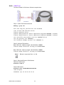
7" LED PANEL 400N 800X480(G), AUO G070VW01 V0
(P/N: 96LEDK-A070WV40NB1)
LCD Backlight Cable (P/N: 1700021882-01)
LVDS Cable (P/N: 1700021883-01)
Cable Kit (P/N: ROM-AC7500-0CA1E)
A CABLE SATA 15P/1*4P-2.5 40cm for ROM-DB7500 (P/N: 1700021941-01)
M Cable SATA 7P/SATA 7P 8CM C=R 180/180 (P/N:1700004711)
Mini USB Host Cable (P/N: 1700019076)
Mini USB Client Cable (P/N: 1700019077)
USB 4 pin to Type A Cable (P/N: 1700021861-01)
F Cable IDE#2 10P-2.0/D-SUB 9P(M) 25CM (P/N: 1700100250)
Terminal connector 9P Female (P/N: 1654909900)
Accessories (Optional)
SQFlash SD Card SLC 2G, 2CH(-40~85°C) (P/N: SQF-ISDS2-2G-ETE)
802.11 b/g/n,AR9287,2T2R,Full size Mini PCIe (P/N: EWM-W142F01E)
Cellular, HSUPA/WCDMA/GPRS, Full Mini PCIe (P/N: EWM-C106FT01E)
Antenna Coaxial Cable SMA/MHF 10cm(P/N: 1750005583)
Antenna SMA D(M) JACK to I-PEX MHF CABLE L:100mm (P/N: 1750006233)
Heatsink O-Freescale-S-5W 70x63x8-SC ROM-7420-60
(P/N: 1960061913N001)
ADAPTER 100-240V 36W 12V 3A (P/N: 1757003553)
Power Cord (Optional)
3 pin Power Cord for USA standard (P/N: 1700001524)
3 pin Power Cord for Europe standard (P/N: 170203183C)
3 pin Power Cord for UK standard (P/N: 170203180A)
iii
ROM-7420 User Manual
Safety Instructions
1.
2.
3.
Read these safety instructions carefully.
Keep this User Manual for later reference.
Disconnect this equipment from any AC outlet before cleaning. Use a damp
cloth. Do not use liquid or spray detergents for cleaning.
4. For plug-in equipment, the power outlet socket must be located near the equipment and must be easily accessible.
5. Keep this equipment away from humidity.
6. Put this equipment on a reliable surface during installation. Dropping it or letting
it fall may cause damage.
7. The openings on the enclosure are for air convection. Protect the equipment
from overheating. DO NOT COVER THE OPENINGS.
8. Make sure the voltage of the power source is correct before connecting the
equipment to the power outlet.
9. Position the power cord so that people cannot step on it. Do not place anything
over the power cord.
10. All cautions and warnings on the equipment should be noted.
11. If the equipment is not used for a long time, disconnect it from the power source
to avoid damage by transient overvoltage.
12. Never pour any liquid into an opening. This may cause fire or electrical shock.
13. Never open the equipment. For safety reasons, the equipment should be
opened only by qualified service personnel.
14. If one of the following situations arises, get the equipment checked by service
personnel:
The power cord or plug is damaged.
Liquid has penetrated into the equipment.
The equipment has been exposed to moisture.
The equipment does not work well, or you cannot get it to work according to
the user's manual.
The equipment has been dropped and damaged.
The equipment has obvious signs of breakage.
DISCLAIMER: This set of instructions is given according to IEC 704-1. Advantech
disclaims all responsibility for the accuracy of any statements contained herein.
ROM-7420 User Manual
iv
Contents
Chapter
Chapter
1
Product Overview ................................1
1.1
1.2
Introduction ............................................................................................... 2
Features .................................................................................................... 3
2
H/W Installation....................................5
2.1
ROM-7420 Evaluation Kit Hardware Specifications.................................. 6
Table 2.1: ROM-7420 Specification............................................. 6
ROM-7420 Board Block Diagram.............................................................. 7
Figure 2.1 ROM-7420 Block Diagram.......................................... 7
Development Kit H/W Installation.............................................................. 8
Table 2.2: ROM-7420 Development Kit Assembly ...................... 8
Figure 2.2 ROM-7420 Development Kit Assembly ...................... 8
2.3.1 ROM-7420 (Part-A)....................................................................... 9
2.3.2 ROM-DB7500 (Part-B).................................................................. 9
2.3.3 7” LVDS LCD Module (Part-B1).................................................... 9
2.3.4 LCD Backlight Cable (Part-B2) ..................................................... 9
2.3.5 LVDS Cable (Part-B3)................................................................... 9
2.3.6 SQFlash SD Card (Part-C) ........................................................... 9
2.3.7 SATA Power Cable (Part-D1) ....................................................... 9
2.3.8 SATA Cable (Part-D2) .................................................................. 9
2.3.9 Mini USB Host Cable (Part-E)....................................................... 9
2.3.10 Mini USB Client Cable (Part-F) ................................................... 10
2.3.11 USB 4 pin to Type-A Cable (Part-G)........................................... 10
2.3.12 12V Power Adapter (Part-H) ....................................................... 10
2.3.13 COM Port Cable (D-SUB 9P to Housing) (Part-J) ...................... 10
2.3.14 RS-232 Loopback (Part-K).......................................................... 10
ROM-DB7500 Connectors ...................................................................... 10
Table 2.3: ROM-DB7500 onboard connectors and key IC ........ 10
Figure 2.3 ROM-DB7500 Connector Position............................ 11
2.4.1 Back panel connectors................................................................ 12
Figure 2.4 Back Panel connectors............................................. 12
Figure 2.5 DC Jack .................................................................... 12
Figure 2.6 CAN BUS connector................................................. 13
Figure 2.7 VGA connector ......................................................... 14
Figure 2.8 HDMI connector........................................................ 14
Figure 2.9 GPIO connector........................................................ 15
Figure 2.10LAN Jack and USB Port ........................................... 16
Figure 2.11Schematics for Audio Jack ....................................... 16
2.4.2 Internal connectors & headers .................................................... 17
Figure 2.12LVDS connector (40 pins) ........................................ 17
Figure 2.13LVDS Power Connector ........................................... 18
Figure 2.14USB Header ............................................................. 18
Figure 2.15USB OTG ................................................................. 18
Figure 2.16SATA connector ....................................................... 19
Figure 2.17JTAG Pin header ...................................................... 19
Figure 2.18UART Pin header ..................................................... 20
Figure 2.19Mini PCIE.................................................................. 21
Figure 2.20SIM Card connector.................................................. 21
Figure 2.21SD Card connector ................................................... 22
Figure 2.22MXM Connector........................................................ 22
Figure 2.23ROM-7420 Pin location ............................................ 25
Jumper setting......................................................................................... 26
2.5.1 ROM-7420 module board ........................................................... 26
2.2
2.3
2.4
2.5
v
ROM-7420 User Manual
2.6
2.7
2.8
Chapter
2.5.2 ROM-DB7500 Evaluation Carrier Board..................................... 26
Mechanical.............................................................................................. 29
2.6.1 Connector Location..................................................................... 29
Figure 2.24Mechanical Drawing ................................................. 29
Table 2.4: ROM-DB7500 onboard connector............................ 30
2.6.2 ROM-7420 Board Dimension...................................................... 31
Figure 2.25ROM-7420 Board Dimension ................................... 31
2.6.3 ROM-DB7500 Board Dimension................................................. 32
Figure 2.26ROM-DB7500 Board Dimension .............................. 32
Quick Start of ROM-7420........................................................................ 33
2.7.1 Debug Port handling ................................................................... 33
Figure 2.27HyperTerminal Settings for Terminal Setup ............. 35
2.7.2 Power on evaluation board ......................................................... 36
Test Tools ............................................................................................... 37
2.8.1 eMMC Test ................................................................................. 37
2.8.2 SATA Test .................................................................................. 37
2.8.3 USB Test .................................................................................... 38
2.8.4 SD Test....................................................................................... 38
2.8.5 GPIO Test................................................................................... 39
2.8.6 LVDS/HDMI/VGA Test................................................................ 40
2.8.7 I2C Test ...................................................................................... 41
2.8.8 Mini PCIe (3G and Wifi) Test ...................................................... 43
2.8.9 CAN Test .................................................................................... 44
2.8.10 Audio Out and MIC In Test ......................................................... 45
2.8.11 OpenGL Test .............................................................................. 45
2.8.12 LAN Test..................................................................................... 46
2.8.13 RS232 Test................................................................................. 47
2.8.14 Watchdog Timer Test ................................................................. 48
2.8.15 Audio Test................................................................................... 49
2.8.16 Photo Demo Test........................................................................ 49
3
Software Functionality ..................... 51
3.1
Package Content .................................................................................... 52
3.1.1 Pre-built System Image .............................................................. 52
3.1.2 Source Code Package................................................................ 52
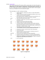
Figure 3.1 Source code package structure................................ 52
Figure 3.2 image\rootfs.............................................................. 54
Set up Build Environment ....................................................................... 56
3.2.1 setenv.sh .................................................................................... 56
Build Instructions..................................................................................... 57
3.3.1 Build u-boot Image...................................................................... 57
3.3.2 Build Linux Kernel Image............................................................ 57
3.3.3 Build Log..................................................................................... 57
Source Code Modification....................................................................... 58
3.4.1 Add a Driver to Kernel by menuconfig ........................................ 58
Figure 3.3 Linux Kernel Configuration ....................................... 58
Figure 3.4 Selecting Seiko Instruments S-35390A.................... 59
3.4.2 Change ROM-7420 Boot Logo ................................................... 60
Create a Linux System Boot Media ........................................................ 60
3.5.1 Create a Linux System SD Card................................................. 60
3.5.2 Boot from Onboard Flash ........................................................... 61
3.5.3 Boot from SATA.......................................................................... 61
Debug Message...................................................................................... 62
Figure 3.5 HyperTerminal Settings for Serial Console Setup.... 62
Linux Software AP and Testing on ROM-7420 ....................................... 63
3.7.1 “Hello World!” Application and Execution ................................... 63
3.7.2 Watchdog Timer Sample Code................................................... 64
3.7.3 GPIO setting ............................................................................... 65
3.2
3.3
3.4
3.5
3.6
3.7
ROM-7420 User Manual
vi
3.7.4
3.7.5
3.7.6
3.7.7
3.7.8
3.7.9
RS232 Initial Code ...................................................................... 66
Display Output Setting ................................................................ 66
Network Setup ............................................................................ 68
Storage (SATA /eMMC/SD card) ................................................ 69
3G Sample Code ........................................................................ 69
I2C Initial Code ........................................................................... 70
Chapter
4
System Recovery...............................71
Chapter
5
Advantech Services ..........................73
5.1
5.2
5.3
RISC Design-in Services......................................................................... 74
Contact Information................................................................................. 76
Global Service Policy .............................................................................. 76
5.3.1 Warranty Policy........................................................................... 76
5.3.2 Repair Process ........................................................................... 77
vii
ROM-7420 User Manual
ROM-7420 User Manual
viii
Chapter
1
1
Product Overview
This chapter briefly introduces
ROM-7420 platform.
1.1 Introduction
In order to offer variable RISC platform requirement and market demand a more efficient and low risk solution, Advantech brings a new RISC module board ROM-7420
to the market. ROM-7420 is a RISC on module (ROM) board solution, with Freescale
i.MX6 processor in ARM® Cortex™ A9 architecture, a complete 64-bit data bus, Dual
Core 1GHz speed SoC engine. It is a high performance module board which is
ready-to-run, compact, and easy-to-expansion which can easily fulfill the features
needed in different vertical markets. With ROM-7420 Freescale ARM Coretex-A9
i.MX6 QSeven Module, you will have flexible I/O interfaces and complete hardware
and software solutions in low cost.
Advantech involves in Computer on modules (COM) development for years and
started RISC-on-Module (ROM) product development since 2010. In order to
strengthen design-in serviceability and speed up the process, we are ready to provide you several hardware design utilities including Schematics Checklist and Layout
Checklist for Carrier board design. You can check your carrier board design in detail
through these tools easily. Advantech also offers Evaluation Carrier Board for every
single RISC-on-Module products and bring you the necessary equipment and S/W
test utility that will help reduce design efforts and speed up application development.
ROM-7420 Evaluation Kit is a complete solution for you to evaluate hardware performance and software capabilities. It includes the board level solution that developers
would need like carrier board and debug port adapter board. With ROM-7420 Evaluation kit, you can start software development in advance and working on carrier
board design in the meantime to reach the target of time to market. With the Cable kit
and Panel kit provided by Advantech, you can connect your own devices to evaluation carrier board for test and integration purpose. Additionally, Advantech brings you
more optional accessories such as Wi-Fi module, 3G module, Antenna and Thermal
solution for project evaluation, application development that minimize the efforts of
compatibility test and driver porting. ROM-7420 Evaluation Kit has already integrated
complete certified functions in Linux kernel 3.0.35, the test utilities and H/W developing tool offered will facilitate the whole process of project development and makes
your project become easy and risk-free.
ROM-7420 User Manual
2
And the main features of Freescale i.MX6 processors are shown as follows:
ARM Cortex™-A9 high performance processor, dual core 1GHz
Supports OpenGL ES 2.0 and OpenVG™ 1.1 hardware accelerators, full HD
1080p video codec
Freescale Smart Speed™ Technology support low power consumption
Capabilities of I/O expansion: UART(4), Dual LVDS, Audio, USB Host, USB
OTG, Gigabit Ethernet, SD, SATA, GPIO(8), I2C, SPI, I2S, CAN bus with 5V
level(2), Mini PCI-E with USB/PCIe signal inside and VGA/HDMI support
Supports SATA storage interface and CAN bus for vehicle application
Supports Linux 3.0.35
Support working temperature 0 ~ 60°C (operation temperature)
Specialized heat spreader design for ROM-7420
3
ROM-7420 User Manual
Product Overview
ROM-7420 adopts Freescale i.MX6 Dual Core Processor - ARM® Cortex™ A9 architecture as its SoC solution. The main features of this platform are followed by
QSeven 1.2 standard, with a heatsink-less, compact, reliable & great power management. Therefore, ROM-7420 platform is suitable for following applications:
HMI (Human Machine Interface)
Portable devices
Fleet management / Navigation
Industrial data collector
Chapter 1
1.2 Features
ROM-7420 User Manual
4
Chapter
2
2
H/W Installation
This chapter introduces the
startup procedures of the ROM7420 hardware, including jumper
setting and device integration. It
also introduces the setting of
switches, indicators and also
shows the mechanical drawings.
Be sure to read all safety precautions before you begin installation
procedure.
2.1 ROM-7420 Evaluation Kit Hardware
Specifications
Table 2.1: ROM-7420 Specification
Item
Description
Kernel
CPU
Freescale i.MX6 Dual 1GHz (ARM Cortex A9)
2D/3D Accelerators
Support OpenGL ES 2.0 and OpenVG™ 1.1 hardware accelerators
System RAM
1GB (Optional: 2GB)
Onboard Flash
4GB (Optional: None)
RTC
Yes
Watchdog Timer
Yes
Reset
H/W reset & S/W reset
I/O
COM
-COM 1, RS-232, 2–wire (TX/RX), Debug port
-COM 2, RS-232, 2–wire (TX/RX), Pin header
-COM 3, RS-232, 2–wire (TX/RX), Pin header
-COM 4, RS-232, 2–wire (TX/RX), Pin header
-COM 5, RS-232, 2–wire (TX/RX), Pin header
Ethernet LAN
1 x 10/100/1000 Gigabit Ethernet (RJ-45)
USB Port
2 x USB 2.0 Type A, 1x USB 2.0 Pin Header
USB OTG
1 x USB 2.0 OTG
SD/MMC
1 x SD/MMC card slot
Mini PCI-E
1 x (Control by USB & PCIe interface)
SIM Card slot
1x
SATA
1x
I2C Interface
3x
I2S Interface
1x
SPI Interface
1x
CAN BUS
2 x 5V level
GPIO
8 x 3.3V TTL level GPIOs
Buzzer control
Yes
Multimedia
Graphic Chip
CPU internal LCD controller
LCD Resolution
Default: 800 x 480 7” WVGA
Optional: 320 x 240 ~ 1920 x 1080
LVDS
2x
HDMI
1x
VGA
1x
Brightness/
Backlight Control
Yes
Audio
Line-out (Stereo) & Mic-in (Stereo)
ROM-7420 User Manual
6
Chapter 2
Power
12V
Power Consumption
Normal Run: 2.5W
Full Run: 5W
Power Control
1 x Power button
1 x Reset button
1 x Sleep mode button
Power Management
-Standard mode
-Sleep mode
Mechanical and Environmental
Board size
ROM-7420: 70x70x5mm (PCB thickness 1.2mm; 10 layers)
ROM-DB7500: 170 x 170 x 30 mm (PCB thickness 1.2mm; 8 layer)
Weight
ROM-7420: 22g
ROM-DB7500:240g
Operation Temperature 0 ~ 60° C (32 ~ 140° F)
Operating Humidity
5% ~ 95% Relative Humidity, non condensing
Vibration
3.5G, 1000 times
Others
RoHS
Yes
Certification
CE/FCC Class B
O.S
Embedded Linux 3.0.35
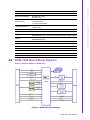
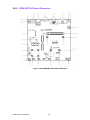
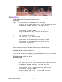
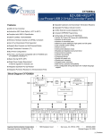
2.2 ROM-7420 Board Block Diagram
Below is the block diagram of ROM-7420.
Figure 2.1 ROM-7420 Block Diagram
7
ROM-7420 User Manual
H/W Installation
DC-input
2.3 Development Kit H/W Installation
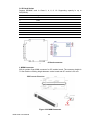
The Figure 2.1 is ROM-7420 Evaluation Kit Assembly, and the detail descriptions and
Advantech P/N are shown below. Please refer to Figure 2.2 and double confirm there
is nothing missing from your evaluation kit.
Table 2.2: ROM-7420 Development Kit Assembly
Item
Description
Advantech P/N
Part-A
ROM-7420
(P/N: ROM-7420CF-A78AAE)
Part-B
ROM-DB7500
(P/N: ROM-DB7500-SC00E)
Part-B1
7” LCD-LED Backlight, LVDS, 800x480
(P/N: 96LEDK-A070WV40NB1)
Part-B2
LCD Backlight Cable
(P/N: 1700021882-01)
Part-B3
LVDS Cable
(P/N: 1700021883-01)
Part-C
SQFlash SD Card, SLC 2GB, (-40~85°C)
(P/N: SQF-ISDS2-2G-ETE)
Part-D1
SATA Power Cable
(P/N: 1700021941-01)
Part-D2
SATA Cable
(P/N: 1700004711)
Part-E
Mini USB Host Cable
(P/N: 1700019076)
Part-F
Mini USB Client Cable
(P/N: 1700019077)
Part-G
USB 4 pin to Type A Cable
(P/N: 1700021861-01)
Part-H
ADAPTER, 100-240V, 12V, 3A.
(P/N: 1757003553)
Part-I
3Pin Power Cord (USA Standard) [Optional]
3pin Power Cord (Europe standard) [Optional]
3pin Power Cord (UK standard) [Optional]
(P/N: 1700001524)
(P/N: 170203183C)
(P/N: 170203180A)
Part-J
COM Port Cable
(P/N: 1700100250)
Part-K
RS-232 Loopback
(P/N: 1654909900)
Figure 2.2 ROM-7420 Development Kit Assembly
ROM-7420 User Manual
8
ROM-7420 is a cost-effective, low-power, and high-performance Q7 module board
without heatsink, geared to satisfy the needs for various industrial computing equipment. Based on Freescale i.MX6 Processor - ARM® CortexTM A9 architecture, there
are DDR3, iNAND flash and other main ICs. ROM-7420 is simple assembly, compact
size, fanless module board with extremely low power consumption.
2.3.2 ROM-DB7500 (Part-B)
2.3.3 7” LVDS LCD Module (Part-B1)
The 7.0 inch Color TFT-LCD Module designed with wide viewing angle; wide operating temperature and long life LEDs backlight is well suited to be the display units for
Industrial Applications. LED driving board for backlight unit is included in this panel
and the structure of the LED units is replaceable. It’s built in timing controller and
LVDS interface. The display supports the WVGA (800 (H) x 480(V)) screen format
and 16.2M colors (RGB 24bits) or 262K (RGB 18bits) selectable.
2.3.4 LCD Backlight Cable (Part-B2)
The LVDS backlight cable connects ROM-DB7500 (LVDS PWR1&LVDS PWR2) with
the LCD backlight connector of 7” LVDS LCD Module.
2.3.5 LVDS Cable (Part-B3)
The LVDS cable connects ROM-DB7500 LVDS connector (LVDS1&LVDS2) with the
LCD signal connector of 7” LVDS LCD Module.
2.3.6 SQFlash SD Card (Part-C)
The SQFlash SD card is a standard SD device. It is the flash-based solid-state drive
available and uses SLC NAND flash memory, making it ideal as an embedded SSD
solution. It connects on SD1 of ROM-DB7500.
2.3.7 SATA Power Cable (Part-D1)
The SATA power cable provides the power signal for SATA HDD by connecting ROMDB7500 (CN4) with the SATA HDD.
2.3.8 SATA Cable (Part-D2)
The SATA cable provides the control signal with SATA HDD by connecting ROMDB7500 (CN3) with the SATA HDD. ROM-DB7500 supports only up to SATA2 (3.0
GB), no SATA3 support.
2.3.9 Mini USB Host Cable (Part-E)
The mini USB Host cable connects ROM-DB7500 (USB_OTG1) with one USB client
device. For example, USB mouse/keyboard or flash disk.
9
ROM-7420 User Manual
H/W Installation
ROM-DB7500 is an evaluation carrier board in MiniITX form factor, which is designed
for Advantech RISC QSeven module only. There are 2 LVDS, 1 VGA, 1 HDMI, 4 USB
(2x USB Type A, 1 x USB OTG, 1x 4-pin connector), 2 CAN bus with 5V level, 4
UART (2wire Tx Rx, 3.3V level), Mini PCIe slot, LAN jack and audio jack for MIC/
speaker test. It also has built in SIM slot for 3G module and onboard SD/eMMC card
slot as extra storage. For data storage, ROM-DB7500 supports SATA2 interface so
user can connect SATA hard disk to evaluation board directly. For more detail regarding ROM-DB7500, please refer to ROM-DB7500 datasheet.
Chapter 2
2.3.1 ROM-7420 (Part-A)
2.3.10 Mini USB Client Cable (Part-F)
The mini USB Client cable connects ROM-DB7500 (USB_OTG1) with PC or NB.
They can recognize ROM-DB7500 in Windows system.
2.3.11 USB 4 pin to Type-A Cable (Part-G)
This USB adapter cable extends USB Type-A from USB 4-pin pin header on board.
You can connect USB mouse/keyboard to ROM-DB7500 through this cable.
2.3.12 12V Power Adapter (Part-H)
The AC-to-DC power device provides a 12V DC output (36W max) with constant voltage sources (100V~240V).
2.3.13 COM Port Cable (D-SUB 9P to Housing) (Part-J)
The cable is used to extend COM port pin header from ROM-DB7500 to D-SUB 9P
serial port connector.
2.3.14 RS-232 Loopback (Part-K)
The loopback terminal is used for test purpose only.
2.4 ROM-DB7500 Connectors
The following table shows the connector and key IC on ROM-DB7500.
Table 2.3: ROM-DB7500 onboard connectors and key IC
Connector
Description
A
CYPRESS , CY7C65630-56LFXA, 4 Port USB Hub, 56-pin QFN 8 × 8 mm
B
Freescale, SGTL5000, I2S Audio Codec, 32-pin QFN 5.0 x 5.0 mm QFN
C
D-SUB 15-pin VGA female connector
D
HDMI Connector
E
Stacked USB+RJ45 receptacle connector with GbE Transformer & LED
F
D-SUB 9-pin Can Bus male connector
G
D-SUB 9-pin GPIO Port female connector
H
2-port Audio Jack
I
DC-in Jack
J
MXM 230-pin socket for module board
K
LVDS Data Connector – 40-pin
L
LVDS Inverter Power Connector -5-pin
M
PCI-E X1 Mini Card connector
N
SIM Card 6 pin Connector
O
SD Card Connector
P
USB 1x5 OTG Connector
Q
USB 1x4 2.54mm pin header (Black)
R
SATA 7-pin signal connector (Blue)
T
I2C 1x4 2.0mm Header
U
JTAG 2x10 2.54mm Header
V
UART Terminal Connector
W
System Fan Header
X
Front Panel Header
ROM-7420 User Manual
10
Y
Main Power Connector (ATX 24 pin PSU connector)
Z
Power Connector (ATX 4 pin PSU connector)
AA
Battery Holder
AB
Power On Button
AC
Sleep Button
AD
Reset Button
AE
Watchdog Trigger Button
Figure 2.3 ROM-DB7500 Connector Position
11
ROM-7420 User Manual
H/W Installation
Below is the corresponding on board connectors mentioned in above table:
Chapter 2
Table 2.3: ROM-DB7500 onboard connectors and key IC
2.4.1 Back panel connectors
There are several connectors located in the back panel of ROM-DB7500. Since
ROM-DB7500 is in mini-ITX form factor, it can fit any mechanical chassis specialized
for miniITX form factor. As a result, below back panel I/Os were reserved for systemleveled integration.
Figure 2.4 Back Panel connectors
Item
Description
P/N
A
DC Jack
1652005624
B
CAN Bus 1
1654009494
C
CAN Bus 2
1654009494
D
VGA Port
1654010443
E
HDMI Port
1654010528-01
F
GPIO Port
1654008866
G
NIC Port 0 (GbE)
1652003674
H
USB 2.0 Port 2 (lower) and 1 (upper)
1652003674
I
Line-Out Port
1652005286
J
MIC-In Port
1652005286
A. DC Jack Connector
Please apply 12V power adapter through this connector.
Pin
Signal
1
+12V
Shield
GND
Figure 2.5 DC Jack
ROM-7420 User Manual
12
Pin
Signal
1
2
D-
3
Chapter 2
B&C CAN Bus
2 CAN buses with 5V level. The connector being used is standard DB9 in male.
4
GND
6
GND
7
D+
H/W Installation
5
8
9
Figure 2.6 CAN BUS connector
D.VGA
Standard VGA connector, VGA support is up to 1920x1080P
Pin
Signal
1
RED
2
GREEN
3
BLUE
4
5
GND
6
GND
7
GND
8
GND
9
+5V
10
GND
11
12
DDC DATA
13
HSYNC
14
VSYNC
15
DDC CLK
13
ROM-7420 User Manual
Figure 2.7 VGA connector
E.HDMI
ROM-DB7500 HDMI follow HDMI 2.0 Spec, supported resolution is up to 1920x1080.
Pin
Signal
1
TMDS_LANE2+
2
GND
3
TMDS_LANE2-
4
TMDS_LANE1+
5
GND
6
TMDS_LANE1-
7
TMDS_LANE0+
8
GND
9
TMDS_LANE0-
10
TMDS_CLK+
11
GND
12
TMDS_CLK-
13
14
15
DDC CLK
16
DDC DAT
17
GND
18
+5V
19
HPD
Figure 2.8 HDMI connector
ROM-7420 User Manual
14
Signal
1
GPI_0
2
GPI_1
3
GPI_2
4
GPI_3
5
GND
6
GPO_0
7
GPO_1
8
GPO_2
9
GPO_3
H/W Installation
Pin
Chapter 2
F.GPIO
9 pins GPIO controlled by software
Figure 2.9 GPIO connector
G&H. RJ45 + USB connector
RJ45 with 10/100/1000 Ethernet plus two USB 2.0 Type A connectors.
Pin
Signal
1
CT
2
MDI0+
3
MDI0-
4
MDI1+
5
MDI1-
6
MDI2+
7
MDI2-
8
MDI3+
9
MDI3-
10
GND
11
ACTIVE LED -
12
ACTIVE LED +
13
LINK 1000 -
14
LINK 100 -
15
+5V
16
USB PORT 2 -
17
USB PORT 2 +
18
GND
19
+5V
20
USB PORT 1 -
21
USB PORT 1 +
22
GND
15
ROM-7420 User Manual
Figure 2.10 LAN Jack and USB Port
I&J. Audio
The red one is Line in and the port in lime is for earphone/speaker out.
Pin
Signal
1
GND
2
3
4
5
MIC in
?
22
HP L
23
24
25
HP R
Figure 2.11 Schematics for Audio Jack
ROM-7420 User Manual
16
ROM-DB7500 also supports several functions through on board connector/pin
header. These connector and pin header may not be placed in the coastline of evaluation boar but they are still located in the appropriate place for better accessibility.
K. LVDS Data Connector – 40-pin
Please also refer to jumper setting in page 10 before connecting LVDS panel.
Signal Name
Pin
Signal Name
1
VCC
21
LVDS_A2+
2
VCC
22
NC
3
GND
23
GND
4
GND
24
GND
5
VCC
25
LVDS_CLKA-
6
VCC
26
NC
7
LVDS_A0-
27
LVDS_CLKA+
8
NC
28
NC
9
LVDS_A0+
29
GND
10
NC
30
GND
11
GND
31
LVDS_DDC_CLK
12
GND
32
LVDS_DDC_DATA
13
LVDS_A1-
33
GND
14
NC
34
GND
15
LVDS_A1+
35
LVDS_A3-
16
NC
36
NC
17
GND
37
LVDS_A3+
18
GND
38
NC
19
LVDS_A2-
39
RSVD
20
NC
40
LVDSA_CTRL
Figure 2.12 LVDS connector (40 pins)
17
ROM-7420 User Manual
H/W Installation
Pin
Chapter 2
2.4.2 Internal connectors & headers
L. LVDS Inverter Power Connector
Please also refer to jumper setting in page 10 before connecting LVDS panel.
Pin
Signal Name
1
+12V
2
GND
3
BKL_EN
4
BKL_CTL
5
+5V
Figure 2.13 LVDS Power Connector
Q. Front Panel USB Header
This pin header is for USB extension of the USB port(s) in the front panel of the miniATX Chassis. We provide adapter cable along with ROM-7420 evaluation kit for
device integration.
Pin
Signal Name
1
+5 VDC
2
D-
3
D+
4
Ground
Figure 2.14 USB Header
P. USB OTG
Standard mini USB connector is used for USB OTG support. Users can connect
ROM-7420 evaluation kit to desktop/laptop PC through this connector.
Pin
Signal Name
1
+5V
2
USB OTG D -
3
USB OTG D +
4
OTG ID
5
GND
Figure 2.15 USB OTG
ROM-7420 User Manual
18
Pin
Signal Name
Description
1
GND
Ground
2
TXP
Transmit diff data - positive
3
TXN
Transmit diff data - negative
GND
Ground
5
RXN
Receive diff data - negative
6
RXP
Receive diff data - positive
7
GND
Ground
H/W Installation
4
Chapter 2
R. SATA Connectors
Standard SATA connector support SATA2 (3.0/bps).
Figure 2.16 SATA connector
U. JTAG
JTAG is reserved for R&D used. Pin out is defined as below:
Pin
Signal Name
Pin
Signal Name
1
VREF
2
+3.3V
3
TRST#
4
Ground
5
TDI
6
Ground
7
TMS
8
Ground
9
TCK
10
Ground
11
RTCK
12
Ground
13
TDO
14
Ground
15
SRST#
16
Ground
17
DBGRQ
18
Ground
19
DACK
20
Ground
Figure 2.17 JTAG Pin header
19
ROM-7420 User Manual
V. UART
ROM-7420 supports only 2-wire UART (Tx,Rx, 3.3V level). We reserve pin header on
ROM-DB7500 for device integration.
Pin
Signal Name
1
2
3
Serial DATA input
4
5
Serial DATA output
6
7
8
9
Ground
10
Figure 2.18 UART Pin header
M. Mini PCI-E
Full size mini PCIe slot supports both USB and PCIe interface. If the Wi-Fi card is
only half-sized, please purchase extending bracket (P/N:1960047454N000) for Wi-Fi
card fixing.
Pin
Signal Name
Pin
Signal Name
1
WAKE#
2
3.3Vaux
3
Reserved
4
GND
5
Reserved
6
1.5V
7
CLKREQ#
8
UIM_PWR
9
GND
10
UIM_DATA
11
REFCLK-
12
UIM_CLK
13
REFCLK+
14
UIM_RESET
15
GND
16
UIM_VPP
Mechanical Key
17
Reserved (UIM_C8)
18
GND
19
Reserved (UIM_C4)
20
W_DISABLE#
21
GND
22
PERST#
23
PERn0
24
3.3Vaux
25
PERp0
26
GND
27
GND
28
1.5V
29
GND
30
SMB_CLK
31
PETn0
32
SMB_DATA
33
PETp0
34
GND
35
GND
36
USB_D-
37
GND
38
USB_D+
39
3.3VAUX
40
GND
41
3.3VAUX
42
LED_WWAN#
ROM-7420 User Manual
20
GND
44
LED_WLAN#
45
Reserved
46
LED_WPAN#
47
Reserved
48
1.5V
49
Reserved
50
GND
51
Reserved
52
3.3VAUX
Chapter 2
43
H/W Installation
Figure 2.19 Mini PCIE
N. SIM Socket
On board SIM socket is for 3G integration. Please insert valid SIM card to dial to 3G
network.
Pin
Signal Name
Pin
Signal Name
5
GND
1
UIM POWER
6
UIM VPP
2
UIM RESET
7
UIM DATA
3
UIM CLK
8
4
Figure 2.20 SIM Card connector
21
ROM-7420 User Manual
O. SD Card Socket
Support SD/MMC card in Class 2, 4, 6, 8, 10. Supporting capacity is up to
32G(SDHC).
Pin
Signal Name
1
DAT3
2
CMD
3
GND
4
+3.3V
5
CLK
6
GND
7
DAT0
8
DAT1
9
DAT2
Figure 2.21 SD Card connector
J. MXM Connector
230 pin golden finger MXM connector for Q7 module board. The connector height is
7.8 mm and the resulting height between carrier board and Q7 module is 5.0 mm.
Figure 2.22 MXM Connector
ROM-7420 User Manual
22
Signal Name
Pin
1
Signal Name
2
GBE_MDI3_N
4
GBE_MDI2_N
5
GBE_MDI3_P
6
GBE_MDI2_P
7
GBE_LINK100#
8
GBE_LINK1000#
9
GBE_MDI1_N
10
GBE_MDI0_N
11
GBE_MDI1_P
12
GBE_MDI0_P
14
GBE_ACT#
13
15
16
TP
17
18
CB_PWR_EN
19
20
PWR_BTN#
21
GBE_CTREF
SLP_BTN#
22
23
24
KEY
25
26
PWRGD_IN
27
28
RST_BTN#
29
SATA0_TX_P
30
31
SATA0_TX_N
32
33
SATA_ACT#
34
35
SATA0_RX_P
36
37
SATA0_RX_N
38
39
40
41
42
SDIO_CLK
44
SDIO_LED
43
SDIO_CD#
45
SDIO_CMD
47
46
SDIO_WP
48
SDIO_DATA1
SDIO_DATA3
49
SDIO_DATA0
50
51
SDIO_DATA2
52
53
54
55
56
57
58
59
GND
I2S_SCLK
60
61
I2S_LRCLK
62
63
AUDIO_CLK
64
65
I2S_DIN
66
I2C1_SCLK
67
I2S_DOUT
68
I2C1_SDAT
69
70
WDTO#
71
72
73
74
75
UART4_TXD
77
UART4_RXD
76
UART3_TXD
78
UART3_RXD
79
80
81
82
83
84
85
86
87
88
23
ROM-7420 User Manual
H/W Installation
3
Chapter 2
Pin
89
90
91
92
USB_OTG_ID
94
USB_HOST_N
96
USB_HOST_P
93
USB_OTG_N
95
USB_OTG_P
97
98
99
LVDS0_TX0_P
100
LVDS1_TX0_P
101
LVDS0_TX0_N
102
LVDS1_TX0_N
103
LVDS0_TX1_P
104
LVDS1_TX1_P
105
LVDS0_TX1_N
106
LVDS1_TX1_N
107
LVDS0_TX2_P
108
LVDS1_TX2_P
109
LVDS0_TX2_N
110
LVDS1_TX2_N
111
LVDS_PWR_EN
112
LVDS_BKL_EN
113
LVDS0_TX3_P
114
LVDS1_TX3_P
115
LVDS0_TX3_N
116
LVDS1_TX3_N
117
118
119
LVDS0_CLK_P
120
LVDS1_CLK_P
121
LVDS0_CLK_N
122
LVDS1_CLK_N
123
LVDS_BKL_CTL
124
CPU_CARD_DETECT#
125
LVDS_DID_DAT
126
LVDS_BLC_DAT
127
LVDS_DID_CLK
128
LVDS_BLC_CLK
129
CAN0_TX
130
CAN0_RX
131
HDMI_CLK_P
132
UART1_TXD
133
HDMI_CLK_N
134
UART1_RXD
135
136
137
HDMI_TD1_P
138
UART2_TXD
139
HDMI_TD1_N
140
UART2_RXD
141
142
143
HDMI_TD0_P
144
CAN1_TX
145
HDMI_TD0_N
146
CAN1_RX
147
148
149
HDMI_TD2_P
150
HDMI_CTRL_DAT
151
HDMI_TD2_N
152
HDMI_CTRL_CLK
153
HDMI_HPD
154
HDMI_CEC_IN
155
PCIE0_CLK_P
156
PCIE_WAKE#
157
PCIE0_CLK_N
158
PCIE_RST#
161
GPO_0
162
GPI_0
163
GPO_1
164
GPI_1
159
160
165
166
167
GPO_2
168
GPI_2
169
GPO_3
170
GPI_3
171
172
173
174
175
176
177
178
W_DISABLE#
179
PCIE0_TX_P
180
PCIE0_RX_P
181
PCIE0_TX_N
182
PCIE0_RX_N
183
ROM-7420 User Manual
184
24
VGA_R
186
VGA_DDC_CLK
187
VGA_G
188
VGA_DDC_DAT
189
VGA_B
190
VGA_VSYNC
192
VGA_HSYNC
+VCC_RTC
194
SPKR
191
193
195
196
197
198
SPI_MOSI
200
SPI_CS0#
201
SPI_MISO
202
SPI_CS1#
203
SPI_SCK
204
JTAG_TRST#
205
+V5SB
206
+V5SB
207
JTAG_TCK
208
JTAG_TDI
209
JTAG_TDO
210
JTAG_TMS
211
+5V
212
213
+5V
214
215
+5V
216
217
+5V
218
219
+5V
220
221
+5V
222
223
+5V
224
225
+5V
226
227
+5V
228
229
+5V
230
Figure 2.23 ROM-7420 Pin location
25
ROM-7420 User Manual
H/W Installation
199
Chapter 2
185
2.5 Jumper setting
There is one switch on ROM-7420 and several jumpers/switches on ROM-DB7500,
this section is to introduce the function of each jumper/switch.
2.5.1 ROM-7420 module board
SW2
Boot Rom Selection
Part Number
1600000202
Footprint
SW_2x2P_50_161X315
Description
DIP SW CHS-02TB(20) SMD 4P SPST P=1.27mm W=5.4mm
Pin
Pin Name
1
+3V
2
GND
This switch is designed for selecting boot up method. With Switch 1 on and Switch 2
off, the board can boot to the Linux OS stored in onboard flash.
Boot Rom selection
SW2
1
2
SPI NOR
ON
OFF
2.5.2 ROM-DB7500 Evaluation Carrier Board
2.5.2.1 LVDS Power
LVDS_VDD_SLT1
Panel power Setting
Description
Panel power for LVDS1
Setting
Function
(1-2)
+3.3V
(3-4)
+5V
(5-6)
+12V
*
LVDS_VDD_SLT2
Panel power Setting
Description
Panel power for LVDS2
Setting
Function
ROM-7420 User Manual
26
+3.3V
(3-4)
+5V
(5-6)
+12V
Chapter 2
(1-2)
*
LVDS_BKLT_SLT1
Backlight power Setting
Description
Panel power for LVDS_PWR1
Setting
Function
(1-2)
+5V
(2-3)
+12V
LVDS_BKLT_SLT2
Backlight power Setting
Description
Panel power for LVDS_PWR2
Setting
Function
(1-2)
+5V
(2-3)
+12V
H/W Installation
2.5.2.2 LVDS Backlight Power
*
*
2.5.2.3 CAN bus
CN19
connect 120ohm termination resistor for CAN0
Description
connect 120ohm termination resistor for CAN0
Setting
Function
(1-2)
connect 120ohm termination resistor for CAN0
CN20
connect 120ohm termination resistor for CAN1
Description
connect 120ohm termination resistor for CAN1
Setting
Function
27
ROM-7420 User Manual
(1-2)
connect 120ohm termination resistor for CAN1
2.5.2.4 SPI NOR Flash
CN21
chip select for SPI NOR flash
Description
chip select for SPI NOR flash
Setting
Function
(1-2)
connect SPI CS0# to SPI NOR flash chip select
(3-4)
connect SPI CS1# to SPI NOR flash chip select
2.5.2.5 Module insertion detect
CN17
Module insertion detect
Description
Module insertion detect
Setting
Function
(1-2)
enable module insertion detect function
ROM-7420 User Manual
28
*
Chapter 2
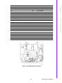
2.6 Mechanical
2.6.1 Connector Location
H/W Installation
Figure 2.24 Mechanical Drawing
29
ROM-7420 User Manual
Table 2.4: ROM-DB7500 onboard connector
Item
Description
P/N
C
D-SUB 15-pin VGA female connector
1654010443
D
HDMI Connector
1654010528-01
E
Stacked USB+RJ45 receptacle connector with GbE
Transformer & LED
1652003674
F
D-SUB 9-pin Can Bus male connector
1654009494
G
D-SUB 9-pin GPIO Port female connector
1654008866
H
2-port Audio Jack
1652005286
I
DC-in Jack
1652005624
J
MXM 230-pin socket for module board
1654005496
K
LVDS Data Connector – 40-pin
1653920200
L
LVDS Inverter Power Connector -5-pin
1655000453
M
PCI-E X1 Mini Card connector
1654002538
N
SIM Card 6 pin Connector
1654004680
O
SD Card Connector
1654009446
P
USB 1x5 OTG Connector
1654000160
Q
USB 1x4 2.54mm pin header (Black)
1655002322
R
SATA 7-pin signal connector (Blue)
1654005955
T
I2C 1x4 2.0mm Header
1655001154
U
JTAG 2x10 2.54mm Header
1653010200
V
UART Terminal Connector
1653004789
W
System Fan Header
1653003100
X
Front Panel Header
1653005202
Y
Main Power Connector (ATX 24 pin PSU connector)
1655000077
Z
Power Connector (ATX 4 pin PSU connector)
1655004584-01
AA
Battery Holder
1750299010
AB
Power On Button
1600000073
AC
Sleep Button
1600000073
AD
Reset Button
1600000073
ROM-7420 User Manual
30
Chapter 2
2.6.2 ROM-7420 Board Dimension
H/W Installation
Figure 2.25 ROM-7420 Board Dimension
31
ROM-7420 User Manual
2.6.3 ROM-DB7500 Board Dimension
Figure 2.26 ROM-DB7500 Board Dimension
ROM-7420 User Manual
32
2.7.1 Debug Port handling
2.7.1.1 Debug port jumper setting
There are 2 different ways of the debug port jumper setting, please see below for
your information.
Default Jumper setting (recommended)
Put 2 jumpers to the right side of the 6-pin pin header as instruction.
In this case, the 2nd pin of debug port DB9 connector is Tx and the 3rd pin is Rx
33
ROM-7420 User Manual
H/W Installation
1.
Chapter 2
2.7 Quick Start of ROM-7420
2.
Optional Jumper setting
Put 2 jumpers to the left side of the 6-pin pin header as instruction.
In this case, the 2nd pin of debug port DB9 connector is Rx and the 3rd pin is Tx
2.7.1.2 Debug Port connection
1. Connect debug port cable to debug port board follow by instruction.
2.
Connect another side of debug port cable to ROM-7420.
ROM-7420 User Manual
34
Connect RS-232 extension cable to debug port board.
4.
Connect the other side of extension cable to USB-to-RS232 cable then connect
to your PC.
Chapter 2
3.
Figure 2.27 HyperTerminal Settings for Terminal Setup
35
ROM-7420 User Manual
H/W Installation
2.7.1.3 Debug Port setting
ROM-7420 can communicate with a host server (Windows or Linux) by using serial
cables. Common serial communication programs such as HyperTerminal, Tera Term
or PuTTY can be used in this case. The example as below describes the serial terminal setup using HyperTerminal on a Windows host:
1. Connect ROM-7420 with your Windows PC by using a serial cable.
2. Open HyperTerminal on your Windows PC, and select the settings as shown in
Figure 3-6.
3. After the bootloader is programmed on SD card, press “POWER” key to power
up the board. The bootloader prompt is displayed on the terminal screen.
2.7.2 Power on evaluation board
The tolerance of power input is 12V ±5%. Please avoid over voltage.
1. Insert Power adapter connector to DC jack on ROM-DB7500.
2.
Turn on the power switch then you can see the LED light in orange is on.
ROM-7420 User Manual
36
All test tools must be verified on ROM-7420 Evaluation kit, please prepare required
test fixtures before verifying each specified I/O. If you have any problem to get the
test fixture, please contact your Advantech contact window for help.
2.8.1 eMMC Test
0+1 records in
0+1 records out
16 bytes (16 B) copied, 0.000109331 s, 146 kB/s
Step2: Check the data copied to eMMC
#hexdump ‐C /dev/mmcblk0 ‐s 25720832 ‐s 32
01887800 31 32 33 34 35 36 37 38 39 41 42 43 44 45 46 0a |123456789ABCDEF.|
01887810 1d 4f e2 19 d3 05 8b df ab 4a 40 5a c5 23 3c f2 |.O.......J@Z.#<.|
Note!
Please make sure parameter “seek” is equal to 25118 as indicated in
red in above codes. If you create the file to a wrong sector, that may
damage the system.
2.8.2 SATA Test
Step 1: Create a file and copy to SATA
#echo 123456789ABCDEF > test.txt
#dd if=./test.txt of=/dev/sda bs=1024 count=1 seek=25118
0+1 records in
0+1 records out
16 bytes (16 B) copied, 0.000109331 s, 146 kB/s
Step 2: Check the data copied to SATA
#hexdump ‐C /dev/sda ‐s 25720832 ‐s 32
01887800 31 32 33 34 35 36 37 38 39 41 42 43 44 45 46 0a |123456789ABCDEF.|
01887810 1d 4f e2 19 d3 05 8b df ab 4a 40 5a c5 23 3c f2 |................| Note!
Please make sure parameter “seek” is equal to 25118 as indicated in
red in above codes. If you create the file to a wrong sector, that may
damage the system.
37
ROM-7420 User Manual
H/W Installation
Step1: Create a file and copy to eMMC.
#echo 123456789ABCDEF > test.txt
#dd if=./test.txt of=/dev/mmcblk0 bs=1024 count=1 seek=25118
Chapter 2
2.8 Test Tools
2.8.3 USB Test
Step 1: Insert USB flash disk then assure it is in ROM-7420 device list
Step2: Create a file and copy to USB flash disk
#echo 123456789ABCDEF > test.txt
#dd if=./test.txt of=/dev/sda bs=1024 count=1 seek=25118
0+1 records in
0+1 records out
16 bytes (16 B) copied, 0.000109331 s, 146 kB/s
Step 3: Check the data copied to USB flash disk
#hexdump ‐C /dev/sda ‐s 25720832 ‐s 32
01887800 31 32 33 34 35 36 37 38 39 41 42 43 44 45 46 0a |123456789ABCDEF.|
01887810 1d 4f e2 19 d3 05 8b df ab 4a 40 5a c5 23 3c f2 |................| Note!
This operation may damage the data stored in USB flash disk. Please
make sure there is no critical data in the USB flash disk being used for
this test.
2.8.4 SD Test
Step 1: When booting from eMMC, you would see only below directories:
#ls /dev/mmcblk*
/dev/mmcblk0 /dev/mmcblk0boot0 /dev/mmcblk0boot1 /dev/mmcblk0p1
Step 2: Insert SD card to SD card slot (SD1) and check your device again. You
should be able to see more directories. /dev/mmcblk1 is the SD card storage.
#ls /dev/mmcblk*
/dev/mmcblk0 /dev/mmcblk0boot1 /dev/mmcblk1 /dev/mmcblk1p2
/dev/mmcblk0boot0 /dev/mmcblk0p1 /dev/mmcblk1p1
Step 3: Create a file and copy to SD
#echo 123456789ABCDEF > test.txt
#dd if=./test.txt of=/dev/mmcblk1 bs=1024 count=1 seek=25118
0+1 records in
0+1 records out
16 bytes (16 B) copied, 0.000109331 s, 146 kB/s
ROM-7420 User Manual
38
#hexdump ‐C /dev/mmcblk1 ‐s 25720832 ‐s 32
01887800 31 32 33 34 35 36 37 38 39 41 42 43 44 45 46 0a |123456789ABCDEF.|
01887810 1d 4f e2 19 d3 05 8b df ab 4a 40 5a c5 23 3c f2 |................| Note!
2.8.5 GPIO Test
2.8.5.1 ROM-7420 GPIO default setting
DSUB 9
Name
path
1
GPI_0
../gpio171
2
GPI_1
../gpio174
3
GPI_2
../gpio175
4
GPI_3
../gpio176
6
GPO_0
../gpio57
7
GPO_1
../gpio55
8
GPO_2
../gpio56
9
GPO_3
../gpio130
#cd /sys/class/gpio
You can use “ls” to list all GPIO devices, and you should also see GPIO ports in
above table.
2.8.5.2 GPIO Test Fixture
Prepare D-Sub9 (male) for ROM-7420, the circuit of this test fixture is shown below.
39
ROM-7420 User Manual
H/W Installation
Please make sure parameter “seek” is equal to 25118 as indicated in
red in above codes. If you create the file to a wrong sector, that may
damage the system.
Chapter 2
Step 4: Check if the file is created successfully.
2.8.5.3 Example of testing GPIO
A. Set gpio57 GPI (in)
#echo in > /sys/class/gpio/gpio57/direction
#cat ./gpio57/direction
in
B. Set gpio171 GPO (out)
#echo out > /sys/class/gpio/gpio171/direction
#cat ./gpio171/direction
out
C. Set gpio171 GPO value “0”
#echo 0 > /sys/class/gpio/gpio171/value
D. Get gpio57 GPI value “0”
#cat ./gpio57/value
0
As you can see in below procedure A and B, we set gpio 57 as GPI and gpio 171 as
GPO so once we send data out from gpio 171, it should be able to receive the same
data from gpio 57
2.8.6 LVDS/HDMI/VGA Test
2.8.6.1 Testing through gplay (for default single display)
Step 1: #gplay /tools/Advantech.avi
Step 2: Then you can see the video demo on the default display screen.
ROM-7420 User Manual
40
Step1: Turn ON the HDMI display, please type as below
#gst‐launch playbin2 uri=file:///tools/Advantech.avi sink="mfw_v4lsink device=/dev/video16"&
video‐
A. Plughw:0? Output the audio through audio jack (AUDIO1)
#gst‐launch playbin2 uri=file:///tools/Advantech.avi video‐
sink="mfw_v4lsink device=/dev/video17" audio‐sink="alsasink
device=plughw:0"
B. Plughw:1?Output the audio through HDMI.
#gst‐launch playbin2 uri=file:///tools/Advantech.avi video‐
sink="mfw_v4lsink device=/dev/video17" audio‐sink="alsasink
device=plughw:1"
If you’d like to change display monitor, please refer to below table:
HDMI
video17
HDMI overlay
video18
VGA
video19
VGA overlay
video20
LVDS 0
video21
LVDS 1
2.8.7 I2C Test
There are three i2c bus in ROM-7420.
#ls /sys/class/i2c‐dev
i2c‐0 i2c‐1 i2c‐2
#i2cdetect ‐l
i2c‐0 i2c imx‐i2c I2C adapter
i2c‐1 i2c imx‐i2c I2C adapter
i2c‐2 i2c imx‐i2c I2C adapter
41
ROM-7420 User Manual
H/W Installation
Step2: Turn ON VGA display at the same time, please type..
#gst‐launch playbin2 uri=file:///tools/Advantech.avi video‐
sink="mfw_v4lsink device=/dev/video18"&
You can see display independent both show Advantech.avi at the same time.
If you’d like to set the output audio as HDMI out or speaker out, please add the
parameter of plughw:
video16
Chapter 2
2.8.6.2 Testing through gst-launch (for multi-display)
If you’d like to do multiple display such as dual LVDS, VGA and HDMI output , you
should set parameter in uboot first. Please refer to section 3.7.5.3 for more detail.
Once the display method is set up, please follow below instruction run gst-launch to
play video
Please try below command to know if there is any device connected to i2c bus 1.
#i2cdetect ‐y 1
0 1 2 3 4 5 6 7 8 9 a b c d e f
00: ‐‐ ‐‐ ‐‐ ‐‐ ‐‐ ‐‐ ‐‐ ‐‐ ‐‐ ‐‐ ‐‐ ‐‐ ‐‐
10: ‐‐ ‐‐ ‐‐ ‐‐ ‐‐ ‐‐ ‐‐ ‐‐ ‐‐ ‐‐ ‐‐ ‐‐ ‐‐ ‐‐ ‐‐ ‐‐
20: ‐‐ ‐‐ ‐‐ ‐‐ ‐‐ ‐‐ ‐‐ ‐‐ ‐‐ ‐‐ ‐‐ ‐‐ ‐‐ ‐‐ ‐‐ ‐‐
30: ‐‐ ‐‐ ‐‐ ‐‐ ‐‐ ‐‐ ‐‐ ‐‐ ‐‐ ‐‐ ‐‐ ‐‐ ‐‐ ‐‐ ‐‐ ‐‐
40: ‐‐ ‐‐ ‐‐ ‐‐ ‐‐ ‐‐ ‐‐ ‐‐ ‐‐ ‐‐ ‐‐ ‐‐ ‐‐ ‐‐ ‐‐ ‐‐
50: UU ‐‐ ‐‐ ‐‐ ‐‐ ‐‐ ‐‐ ‐‐ ‐‐ ‐‐ ‐‐ ‐‐ ‐‐ ‐‐ ‐‐ ‐‐
60: ‐‐ ‐‐ ‐‐ ‐‐ ‐‐ ‐‐ ‐‐ ‐‐ ‐‐ ‐‐ ‐‐ ‐‐ ‐‐ ‐‐ ‐‐ ‐‐
70: ‐‐ ‐‐ ‐‐ ‐‐ ‐‐ ‐‐ ‐‐ ‐‐
The 0x50 is the HDMI address. So you can try below command to know I2C bus is
work or not.
#i2cdump ‐f ‐y 1 0x50
No size specified (using byte-data access)
0 1 2 3 4 5 6 7 8 9 a b c d e f 0123456789abcdef
00: 00 ff ff ff ff ff ff 00 5a 63 28 25 01 01 01 01 ........Zc(%????
10: 15 15 01 03 80 34 1d 78 2e 2c c5 a4 56 50 a1 28 ?????4?x.,??VP?(
20: 0f 50 54 bf ef 80 b3 00 a9 40 a9 c0 95 00 90 40 ?PT????.?@???.?@
30: 81 80 81 00 71 4f 02 3a 80 18 71 38 2d 40 58 2c ???.qO?:??q8‐@X,
40: 45 00 09 25 21 00 00 1e 00 00 00 ff 00 53 45 32 E.?%!..?.....SE2
50: 31 31 32 31 30 30 33 36 34 0a 00 00 00 fd 00 32 112100364?...?.2
60: 4b 18 53 12 00 0a 20 20 20 20 20 20 00 00 00 fc K?S?.? ...?
70: 00 56 58 32 34 35 31 20 53 45 52 49 45 53 01 ea .VX2451 SERIES??
80: 02 03 22 f1 4f 90 05 04 03 02 07 06 1f 14 13 12 ??"?O???????????
90: 11 16 15 01 23 09 7f 07 83 01 00 00 65 03 0c 00 ????#?????..e??.
a0: 10 00 02 3a 80 18 71 38 2d 40 58 2c 45 00 09 25 ?.?:??q8‐@X,E.?%
b0: 21 00 00 1e 01 1d 80 18 71 1c 16 20 58 2c 25 00 !..?????q?? X,%.
c0: 09 25 21 00 00 9e 01 1d 00 72 51 d0 1e 20 6e 28 ?%!..???.rQ?? n(
d0: 55 00 09 25 21 00 00 1e 8c 0a d0 8a 20 e0 2d 10 U.?%!..????? ?‐?
e0: 10 3e 96 00 09 25 21 00 00 18 02 3a 80 d0 72 38 ?>?.?%!..??:??r8
f0: 2d 40 10 2c 45 80 09 25 21 00 00 1e 00 00 00 a0 ‐@?,E??%!..?...?
ROM-7420 User Manual
42
#i2cdump ‐f ‐y 1 0x50
2.8.8 Mini PCIe (3G and Wifi) Test
The command used to test 3G module is as follows, the supported module P/N is
EWM-C106FT01E.
#3glink Send AT commands...
#send (AT^M)
send (ATDT*99#^M)
expect (CONNECT)
AT^M^M
OK^M
ATDT*99#^M^M
CONNECT
‐‐ got it
………
The command used to test Wi-Fi module is as follows, the supported module P/N is
EWM-W142F01E
#ifconfig wlan0 up
#iwconfig wlan0 essid xxx (xxx means your wifi ESSID name)
#dhclient wlan0
43
ROM-7420 User Manual
H/W Installation
No size specified (using byte-data access)
0 1 2 3 4 5 6 7 8 9 a b c d e f 0123456789abcdef
00: XX XX XX XX XX XX XX XX XX XX XX XX XX XX XX XX XXXXXXXXXXXXXXXX
10: XX XX XX XX XX XX XX XX XX XX XX XX XX XX XX XX XXXXXXXXXXXXXXXX
20: XX XX XX XX XX XX XX XX XX XX XX XX XX XX XX XX XXXXXXXXXXXXXXXX
30: XX XX XX XX XX XX XX XX XX XX XX XX XX XX XX XX XXXXXXXXXXXXXXXX
40: XX XX XX XX XX XX XX XX XX XX XX XX XX XX XX XX XXXXXXXXXXXXXXXX
50: XX XX XX XX XX XX XX XX XX XX XX XX XX XX XX XX XXXXXXXXXXXXXXXX
60: XX XX XX XX XX XX XX XX XX XX XX XX XX XX XX XX XXXXXXXXXXXXXXXX
70: XX XX XX XX XX XX XX XX XX XX XX XX XX XX XX XX XXXXXXXXXXXXXXXX
80: XX XX XX XX XX XX XX XX XX XX XX XX XX XX XX XX XXXXXXXXXXXXXXXX
90: XX XX XX XX XX XX XX XX XX XX XX XX XX XX XX XX XXXXXXXXXXXXXXXX
a0: XX XX XX XX XX XX XX XX XX XX XX XX XX XX XX XX XXXXXXXXXXXXXXXX
b0: XX XX XX XX XX XX XX XX XX XX XX XX XX XX XX XX XXXXXXXXXXXXXXXX
c0: XX XX XX XX XX XX XX XX XX XX XX XX XX XX XX XX XXXXXXXXXXXXXXXX
d0: XX XX XX XX XX XX XX XX XX XX XX XX XX XX XX XX XXXXXXXXXXXXXXXX
e0: XX XX XX XX XX XX XX XX XX XX XX XX XX XX XX XX XXXXXXXXXXXXXXXX
f0: XX XX XX XX XX XX XX XX XX XX XX XX XX XX XX XX XXXXXXXXXXXXXXXX
Chapter 2
If there is nothing connected to HDMI port, the result should be as below:
2.8.9 CAN Test
To make a cable for CAN test, follow the steps below.
Step 1: Check CAN network device
#dmesg | grep can
ahci: SSS flag set, parallel bus scan disabled
vcan: Virtual CAN interface driver
flexcan netdevice driver
flexcan imx6q‐flexcan.0: device registered (reg_base=c09b8000, irq=142)
flexcan imx6q‐flexcan.1: device registered (reg_base=c09e8000, irq=143)
can: controller area network core (rev 20090105 abi 8)
can: raw protocol (rev 20090105)
can: broadcast manager protocol (rev 20090105 t)
Step 2: Activate CAN device
#ip link set can0 up type can bitrate 125000
flexcan imx6q‐flexcan.0: writing ctrl=0x0e312005
#ip link set can1 up type can bitrate 125000
flexcan imx6q‐flexcan.1: writing ctrl=0x0e312005
Note!
Bitrate is supported from 1 to 1M.
Step 3: Send and Receive CAN frames
Receive CAN frames:
#cantest can0 & Send CAN frames
#cantest can1 12345678#123412341234 read 16 bytes
12345678 [6] 12 34 12 34 12 34
ROM-7420 User Manual
44
Chapter 2
2.8.10 Audio Out and MIC In Test
MIC IN command is as follows:
#arecord ‐t wav ‐c 1 ‐r 44100 ‐d 5 2.wav
(44100 is the sample rate)
Audio out command is as follows:
#aplay 2.wav
Please follow below instructions to test OpenGL on ROM-7420 platform:
Step 1: Load kernel module galcore.ko
#modprobe galcore
#lsmod
Module Size Used by
galcore 130655 0
g_serial 23346 0
Step 2: Change path to /opt/viv_samples/vdk
#cd /opt/viv_samples/vdk
#ls tutorial*
tutorial1 tutorial2_es20 tutorial4 tutorial5_es20
tutorial1_es20 tutorial3 tutorial4_es20 tutorial6
tutorial2 tutorial3_es20 tutorial5 tutorial7
Step 3: Run tutorial7 for OpenGL ES 1.1
Using Vertex Buffer Objects (VBO) can substantially increase performance by reducing the bandwidth required to transmit geometry data. Information such vertex, normal vector, color, and so on is sent once to locate device video memory and then
bound and used as needed, rather than being read from system memory every time.
This example illustrates how to create and use vertex buffer objects.
#./tutorial7
Step 4: Run tutorial3_es20 for OpenGL ES 2.0
A ball made of a mirroring material and centered at the origin spins about its Y-axis
and reflects the scene surrounding it.
#./tutorial3_es20
45
ROM-7420 User Manual
H/W Installation
2.8.11 OpenGL Test
2.8.12 LAN Test
ROM-7420 sets DHCP as defaul network portocal.
#ifconfig eth0 Link encap:Ethernet HWaddr 00:04:9F:01:30:E0
inet addr:172.17.21.96 Bcast:172.17.21.255 Mask:255.255.254.0
UP BROADCAST RUNNING MULTICAST MTU:1500 Metric:1
RX packets:129 errors:0 dropped:18 overruns:0 frame:0
TX packets:2 errors:0 dropped:0 overruns:0 carrier:0
collisions:0 txqueuelen:1000
RX bytes:15016 (14.6 KiB) TX bytes:656 (656.0 B)
lo Link encap:Local Loopback
inet addr:127.0.0.1 Mask:255.0.0.0
UP LOOPBACK RUNNING MTU:16436 Metric:1
RX packets:0 errors:0 dropped:0 overruns:0 frame:0
TX packets:0 errors:0 dropped:0 overruns:0 carrier:0
collisions:0 txqueuelen:0
RX bytes:0 (0.0 B) TX bytes:0 (0.0 B)
If you would like to config IP manually, please use the command below:
#ifconfig eth0 xxx.xxx.xxx.xxx up
Here is a real case for your reference.The hosts(ROM-7420) IP is 172.17.21.97; the
target(A desktop computer) IP is 172.17.20.192
#ifconfig eth0 172.17.21.97 up
#ifconfig eth0
eth0 Link encap:Ethernet HWaddr 00:04:9F:01:30:E0
inet addr:172.17.21.97 Bcast:172.17.255.255 Mask:255.255.0.0
UP BROADCAST RUNNING MULTICAST MTU:1500 Metric:1
RX packets:2851 errors:0 dropped:271 overruns:0 frame:0
TX packets:30 errors:0 dropped:0 overruns:0 carrier:0
collisions:0 txqueuelen:1000
RX bytes:291407 (284.5 KiB) TX bytes:2000 (1.9 KiB)
ROM-7420 User Manual
46
PING 172.17.20.192 (172.17.20.192): 56 data bytes
64 bytes from 172.17.20.192: seq=0 ttl=128 time=7.417 ms
64 bytes from 172.17.20.192: seq=1 ttl=128 time=0.203 ms
64 bytes from 172.17.20.192: seq=2 ttl=128 time=0.300 ms
2.8.13 RS232 Test
As you can see below, there are 5 UART supported by ROM-7420. /dev/ttymxc0 is
reserved for ROM-7420 debug port (ROM-7420 CN1), the rest UART ports could be
applied by user.
#setserial ‐g /dev/ttymxc*
/dev/ttymxc0, UART: undefined, Port: 0x0000, IRQ: 58
/dev/ttymxc1, UART: undefined, Port: 0x0000, IRQ: 59
/dev/ttymxc2, UART: undefined, Port: 0x0000, IRQ: 60
/dev/ttymxc3, UART: undefined, Port: 0x0000, IRQ: 61
/dev/ttymxc4, UART: undefined, Port: 0x0000, IRQ: 62 Below test was done with four 2.0mm pitch mini jumpers. Advantech P/N is
1653302122. This mini jumper is a bridge connecting Tx and Rx.
2.8.13.1 /dev/ttymxc1 testing (CN9)
#stty ‐F /dev/ttymxc1 ‐echo
#cat /dev/ttymxc1
[CTRL+Z]
#echo hello > /dev/ttymxc1
#fg
Hello
[CTRL+C]
47
ROM-7420 User Manual
H/W Installation
‐‐‐ 172.17.20.192 ping statistics ‐‐‐
3 packets transmitted, 3 packets received, 0% packet loss
round‐trip min/avg/max = 0.203/2.640/7.417 ms
Chapter 2
The target computer(Client) IP address is 172.17.20.192, so we can use below command to see if we can get any response from the client
#ping 172.17.20.192
2.8.13.2 /dev/ttymxc2 testing (CN11)
#stty ‐F /dev/ttymxc2 ‐echo
#cat /dev/ttymxc2
[CTRL+Z]
#echo hello > /dev/ttymxc2
#fg
Hello
[CTRL+C]
2.8.13.3 /dev/ttymxc3 testing (CN10)
#stty ‐F /dev/ttymxc3 ‐echo
#cat /dev/ttymxc3
[CTRL+Z]
#echo hello > /dev/ttymxc3
#fg
Hello
[CTRL+C]
2.8.13.4 /dev/ttymxc4 testing (CN12)
#stty ‐F /dev/ttymxc4 ‐echo
#cat /dev/ttymxc4
[CTRL+Z]
#echo hello > /dev/ttymxc4
#fg
Hello
[CTRL+C]
2.8.14 Watchdog Timer Test
Step 1: Executing‘ wdt_driver_test.out ‘
#/unit_tests/wdt_driver_test.out
Usage: wdt_driver_test <timeout> <sleep> <test>
timeout: value in seconds to cause wdt timeout/reset
sleep: value in seconds to service the wdt
test: 0 ‐ Service wdt with ioctl(), 1 ‐ with write()
Step 2: Please try below command to set timeout as 10 seconds, system will reboot
after then.
#/unit_tests/wdt_driver_test.out 10 5 0
Starting wdt_driver (timeout: 10, sleep: 5, test: ioctl)
Trying to set timeout value=10 seconds
The actual timeout was set to 10 seconds
Now reading back ‐‐ The timeout is 10 seconds
Press [CTRL+C] then you should be able to see below result:
imx2‐wdt imx2‐wdt.0: Unexpected close: Expect reboot!
Then system will reboot in 10 seconds
ROM-7420 User Manual
48
Execute the following commands to run the Audio demo application on ROM-7420.
#cd /unit_tests
#aplay audio8k16S.wav
Then you can hear the music from speaker/head-sets.
2.8.16 Photo Demo Test
49
ROM-7420 User Manual
H/W Installation
Execute the following commands to run the Photo demo application on ROM-7420.
#cd /tools
#./fbv Advantech.jpg
Then you can see the photo demo on the default display screen.
Chapter 2
2.8.15 Audio Test
ROM-7420 User Manual
50
Chapter
3
3
Software Functionality
This chapter details the Linux
operating system on the ROM7420 platform.
ROM-7420 platform is an embedded system with Linux kernel 3.0.35 inside. It contains all system-required shell commands and drivers ready for ROM-7420 platform.
We do not offer IDE developing environment in ROM-7420 BSP, users can evaluate
and develop under Ubuntu 10.04LTS environment and the BSP for ROM-7420 supports console mode only.
There are three major boot components for Linux, “u-boot.bin”, “uImage” and “File
System”. The “u-boot.bin” is for initializing peripheral hardware parameters; the “uImage” is the Linux kernel image and the “File System” is for Linux O.S. used.
It will not be able to boot into Linux environment successfully if one of above three
files is missing from booting media (SD card, SATA HDD or onboard flash)
The purpose of this chapter is to introduce software development of ROM-7420 to
you, so that you can develop your own application(s) efficiently.
ROM-7420 is designed for supporting Linux host only so you may fail developing
your AP on Windows/Android host PC. For now the official supported host version is
Ubuntu 10.04 LTS, host PC in any other version may have compatibility issue. In this
case, we strongly recommend to have Ubuntu 10.04 LTS installed to your host PC
before start ROM-7420 evaluation/development.
3.1 Package Content
We would offer you two different kinds of Linux package for ROM-7420. One is prebuilt system image for system recovery another is source code package (BSP).
3.1.1 Pre-built System Image
You are able to find the pre-built image 7420LIVXXXX.tar.bz2 from ROM-7420 Evaluation Kit DVD image downloaded from Advantech website. ROM-7420 supports
booting from SD card so you can extract the image to SD card then dump the image
file to onboard eMMC to complete system recovery. For more detail, please refer to
section 3.8 System Recovery.
3.1.2 Source Code Package
ROM-7420 source code package (BSP) contains cross compiler, Linux source code,
Uboot source code, root file system and some scripts used in OS development.
Some of above components are developed by Advantech and the others are developed by open source community. ROM-7420 source code package is composed of
six main folders: “cross_compiler”, “document”, “image”, “package”, “scripts”, and
“source”.
Note!
ROM-7420 source code package (BSP) is Advantech’s Intellectual
Property. If you need to access this package, please contact your
Advantech support window.
Figure 3.1 Source code package structure
ROM-7420 User Manual
52
“cross_compiler” →
This folder contains source code for cross compiler.
“document”
→
This folder contains user guide.
“image”
→
This folder contains the uImage, and the script for making
Linux system media automatically.
“image/rootfs”
→
This folder contains Linux root file system
“package”
→
This folder contains source code provided by Freescale without any modification
“scripts”
→
This folder contains scripts for configure system and compile
images automatically.
“source”
→
This folder contains source code owned by Advantech
3.1.2.1 cross_compiler
You can use the cross compiler toolchain to compile the uImage and related applications. (gcc version is 4.6.2 20110630)
Toolchain directory structure is as follow:
|-- bin // toolchain with prefix, such as arm-none-linux-gnueabi-gcc etc.
|-- lib // library files used for toolchain itself, not for application
|-- arm-fsl-linux-gnueabi
|-- bin // toolchain without prefix, such as gcc.
|-- debug-root // all debug tools
|-- multi-libs // all libraries and headers.
|-- armv5 // library for armv5 (i.mx 2xx). only support soft float point
|-- armv6 // library for armv6 (i.mx 3xx), soft fpu version
|-- armv7-a // library for armv7-a (i.mx5xx and i.mx6xx), hardware fpu version
|-- lib //default library. It can be used for armv4t and above.
|-- usr
|-- include //header files for the application development
|-- lib //three-part library and static built library Freescale
3.1.2.2 document
User guide of how to setup up the environment of development
3.1.2.3 image
This folder includes uImage & u-boot.
53
ROM-7420 User Manual
Software Functionality
Chapter 3
The description of 7420LBVxxxx package contents:
3.1.2.4 image/rootfs
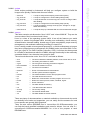
Linux adopts Hierarchical File System (HFS), image/rootfs is the Linux file system in
highest level of the tree structure. image/rootfs is just like the trunk of the tree. Its
sub-directories are the branches and the files in these directories are the leaves of
the tree. image/rootfs contains all subdirectories and files used in the file system,
that’s why it is called the root of the whole file system.
The main folders in “rootfs” are listed as follows:
– bin
→ Common programs, shared by the system, the system administrator
and the users.
– dev
→ Contains references to all the CPU peripheral hardware, which are represented as files with special properties.
– etc
→ Most important system configuration files are in /etc, this directory contains data similar to those in the Control Panel in Windows
– home
→ Home directories of the common users.
– lib
→ Library files, includes files for all kinds of programs needed by the system and the users.
– mnt
→ Standard mount point for external file systems.
– opt
→ Typically contains extra and third party software.
– proc
→ A virtual file system containing information about system resources.
More information about the meaning of the files in proc is obtained by
entering the command man proc in a terminal window. The file proc.txt
discusses the virtual file system in detail.
– root
→ The administrative user's home directory. Mind the difference between /
, the root directory and /root, the home directory of the root user.
– sbin
→ Programs for use by the system and the system administrator.
– sys
→ Linux sys file system
– tmp
→ Temporary space for use by the system, cleaned upon reboot, so
doesn’t use this for saving any work!
– unit_tests
→ unit test tools are provided by Freescale i.MX6 product
– usr
→ Programs, libraries, documentation etc. for all user-related programs.
– var
→ Storage for all variable files and temporary files created by users, such
as log files, the mail queue, the print spooler area, space for temporary
storage of files downloaded from the Internet.
– tools
→ just for sample test.
Figure 3.2 image\rootfs
ROM-7420 User Manual
54
→ A script to setup the developing environment quickly.
– cfg_uboot.sh
→ A script to configure the u-boot building setup quickly.
– mk_uboot.sh
→ A script to build the u-boot and copy the “u-boot” to “image” folder
after building.
– cfg_kernel.sh
→ A script to configure the kernel building setup quickly.
– mk_kernel.sh
→ A script to build the “uImage” and copy the “uImage” to “image”
folder after building.
– mksd-linux.sh
→ A script to setup up a bootable SD card if users build their images
3.1.2.6 source
This folder contains sub-directories “linux-3.0.35” and “u-boot-2009.08”. They are the
source codes of the Linux kernel and U-boot.
Linux is a clone of the operating system UNIX. It has all the features you would
expect in a modern fully-fledged UNIX, including true multitasking, virtual memory,
shared libraries, demand loading, shared copy-on-write executables, proper memory
management, and multitask networking including IPv4 and IPv6.
Linux is easily portable to most general-purpose 32- or 64-bit architectures as long as
they have a paged memory management unit (PMMU) and a port of the GNU C compiler (gcc) (part of The GNU Compiler Collection, GCC). Linux has also been ported
to a number of architectures without a PMMU, although functionality is then obviously
somewhat limited. Linux has also been ported to itself.
The main sub-directories under “linux-3.0.35” are listed as follows:
– arch
→ The items related to hardware platform, most of them are for CPU.
– block
→ The setting information for block.
– crypto
→ The encryption technology that kernel supports.
– Documentation
→ The documentation for kernel.
– drivers
→ The drivers for hardware.
– firmware
→ Some of firmware data for old hardware.
– fs
→ The file system the kernel supports.
– include
→ The header definition for the other programs used.
– init
→ The initial functions for kernel.
– ipc
→ Define the communication for each program of Linux O.S.
– kernel
→ Define the Kernel process, status, schedule, signal.
– lib
→ Some of libraries.
– mm
→ The data related the memory.
– net
→
– security
→ The security setting.
– sound
→ The module related audio.
– virt
→ The data related the virtual machine.
The data related the network.
There are plenty of documentations or materials available on Internet and also could
be obtained from books and magazines, you can easily find the answers for both
Linux-specific and general UNIX questions.
There are also various README files in ./source/linux-3.0.35/Documentation, you
can find the kernel-specified installations and notes for drivers. You can refer to ./
source/linux-3.0.35/Documentation/00-INDEX for a list of the purpose of each
README/note.
55
ROM-7420 User Manual
Software Functionality
– setenv.sh
Chapter 3
3.1.2.5 scripts
Some scripts provided by Advantech will help you configure system or build the
images more quickly. Please check them as follows:
3.2 Set up Build Environment
All instructions in this guide are based on Ubuntu 10.04 LTS developing environment.
Please install the Ubuntu 10.04 LTS at your PC/NB in advance.
When you obtain the ROM-7420 Linux source code package, please refer to following instructions to extract to your developing environment:
1. Copy "7420LBVxxxx.tar.bz2" package to your desktop. “xxxx” is the version of
the BSP source code.
2. Start your "Terminal" on Ubuntu 10.04 LTS.
3. $sudo su (Change to “root” authority)
4. Input user password
5. #cd Desktop/
6. #tar xvf 7420LBVxxxx.tar.bz2 (Unzip file)
7. Then you can see folder "7420LBVxxxx" on desktop.
Advantech offer you a script to setup the developing environment quickly. You can
refer following steps to setup your developing environment:
1. Open "Terminal" on Ubuntu 10.04 LTS.
2. $sudo su (Change to “root” authority)
3. Input user password
4.
5.
6.
#cd Desktop/7420LBVxxxx/scripts/
#. setenv.sh (To configure the developing environment automatically)
Then you can start to code the source code, build images, or compile applications.
3.2.1 setenv.sh
This script is used to configure the developing environment quickly. It will configure
the folder paths for system, and you can also add/modify the setenv.sh by yourself if
you have added/changed the folders and paths.
The major part of setenv.sh is shown as follows:
export SRCROOT=${PWD}/..
export CC_PATH=${SRCROOT}/cross_compiler/fsl‐linaro‐toolchain
export CROSS_COMPILE=${CC_PATH}/bin/arm‐none‐linux‐gnueabi‐
export CC=${CROSS_COMPILE}gcc
export STRIP=${CROSS_COMPILE}strip
export AR=${CROSS_COMPILE}ar
export AS=${CROSS_COMPILE}as
export CXX=${CROSS_COMPILE}g++
export CPP=${CROSS_COMPILE}cpp
export LD=${CROSS_COMPILE}ld
export RANLIB=${CROSS_COMPILE}ranlib
export ARCH=arm
export KROOT=${SRCROOT}/source/linux‐3.0.35
export UBOOT_SOURCE=${SRCROOT}/source/u‐boot‐2009.08
export ROOTFS=${SRCROOT}/image/rootfs
ROM-7420 User Manual
56
Note!
You have to wrap “setenv.sh” once you open a new "Terminal" utility
every time.
(i.e. #source setenv.sh)
Note!
It is suggested to change to “root” authority to use the source code.
This section will guide you how to build the u-boot & Linux kernel.
3.3.1 Build u-boot Image
Advantech has written a script to build the u-boot quickly. You can build u-boot image
by follow below steps:
1. Open "Terminal" on Ubuntu 10.04 LTS..
2. $sudo su (Change to “root” authority)
3. Input user password.
4. #cd Desktop/7420LBVxxxx/scripts/ 5. #. setenv.sh (To configure the developing environment automatically)
6. #./cfg_uboot.sh (To set the u-boot configuration automatically)
7. #./mk_uboot.sh (Start to build the u-boot)
8. Then you can see u-boot_crc.bin and u-boot_crc.bin.crc are being built and
located in ../image.
3.3.2 Build Linux Kernel Image
Advantech offer you a script to build the “uImage” quickly. You can build uImage by
follow below steps:
1. Open "Terminal" on Ubuntu 10.04 LTS.
2. $sudo su (Change to “root” authority)
3. Input user password.
4. #cd Desktop/7420LBVxxxx/scripts/ 5. #. setenv.sh (To configure the developing environment automatically)
6. #./cfg_kernel.sh (To set the uImage configuration automatically)
7. #./mk_kernel.sh (Start to build the uImage)
8. Then you can see uImage is being built and located in ../image.
3.3.3 Build Log
You can find the build log from folder “./7420LBVxxxx”. If you got any error message
when building Linux kernel, it is suggested to look into the log file to learn more detail
about it.
57
ROM-7420 User Manual
Software Functionality
3.3 Build Instructions
Chapter 3
export LOG=${SRCROOT}/Build.log
export PATH=${CC_PATH}/bin:${UBOOT_SOURCE}/tools:$PATH
3.4 Source Code Modification
This section will guide you how to use the Linux source code. You will see some
examples of using BSP source code in this section.
3.4.1 Add a Driver to Kernel by menuconfig
You can add a driver to kernel by menuconfig. Here is an example to guide you how
to add a RTC driver (Seiko Instruments S-35390A) to Linux kernel. Please refer to
the following steps:
1. Open "Terminal" on Ubuntu 10.04 LTS.
2. $sudo su (Change to “root” authority)
3. Input user password.
4. #cd Desktop/7420LBVxxxx/scripts/ 5. #. setenv.sh (To configure the developing environment automatically)
6. #./cfg_kernel.sh menuconfig 7. Then you will see a GUI screen (Linux Kernel Configuration) as below:
Figure 3.3 Linux Kernel Configuration
ROM-7420 User Manual
58
Select “Device Drivers”→”Real Time Clock”, you will see an option “Seiko
Instruments S-35390A” on the list. Choose this option then exit and save your
configuration.
9.
Change directory to “source/linux-3.0.35/arch/arm/mach-mx6”, edit the “boardmx6q_ROM-7420.h” and “board-mx6q_advantech.c”.
Please add below codes to source/linux-3.0.35/arch/arm/mach-mx6/boardmx6q_ROM-7420.h:
/* I2C */
static struct i2c_board_info mxc_i2c0_board_info[] __initdata =
{
{
I2C_BOARD_INFO("sgtl5000", 0x0a),
},
{
I2C_BOARD_INFO("s35390a", 0x30),
},
};
;
Please add below codes to source/linux-3.0.35/arch/arm/mach-mx6/boardmx6q_advantech.c
i2c_register_board_info(0, mxc_i2c0_board_info,
ARRAY_SIZE(mxc_i2c0_board_info));
10. Please refer to former Chapter 3.3.2 to rebuild the kernel with RTC driver (Seiko
Instruments S-35390A) after completing above steps
Note!
If you cannot find the driver for your device from the list, please contact
your hardware vender.
59
ROM-7420 User Manual
Software Functionality
Figure 3.4 Selecting Seiko Instruments S-35390A
Chapter 3
8.
3.4.2 Change ROM-7420 Boot Logo
By default, ROM-7420 shows a boot logo when booting up. You can replace the logo
to whatever your want by following below steps:
1. You have to download “netpbm” corresponding to your OS version from internet
first,
2. Install “netpbm” by typing $sudo apt‐get install netpbm.
3. Prepare your boot logo. For example: bootlogo.png (Under folder Desktop/bootlogo)
Note!
This picture should be in PNG format and less than 224 colors. It is suggested to have the image resolution equal to your LCD panel size.
4.
5.
6.
7.
8.
Open "Terminal" on Ubuntu 10.04 LTS..
$sudo su (Change to “root” authority)
Input user password.
#cd Desktop/bootlogo (Go into the folder that bootlogo.png located)
#pngtopnm bootlogo.png | ppmquant 224 | pnmtoplainpnm > logo_linux_clut224.ppm
9. #cp logo_linux_clut224.ppm \
../7420LBVxxxx/source/linux‐3.0.35/drivers/video/logo/
10. Then you can refer Chapter 3.3.1 to rebuild the kernel with your own boot logo.
3.5 Create a Linux System Boot Media
ROM-7420 supports boot from SD card, SATA device and onboard flash. This section
will guide you how to build a image for ROM-7420 Linux system boot media.
3.5.1 Create a Linux System SD Card
3.5.1.1 From Pre-built System Image
You are able to find the pre-built image from CD included in ROM-7420 Evaluation Kit
(P/N: TBD). Please follow below steps to create a SD card for boot up.
1. Copy “7420LIVxxxx.tar.bz2” package to your desktop.
2. Open "Terminal" on Ubuntu 10.04 LTS..
3. $sudo su (Change to “root” authority)
4. Input your password.
5. #cd Desktop/
6. #tar xvf 7420LIVxxxx.tar.bz2 (Unzip files)
7. Insert one SD card to your developing computer
8. Check the SD card location, like /dev/sdf
9. #cd ./7420LBVxxxx_prebuilt_image
10. #dd if=7420LIVxxxx.img of=/dev/sdf 11. Please wait until dump disk is done
Then insert the Linux system SD card to ROM-7420, it will boot up with Linux environment.
ROM-7420 User Manual
60
If you already have a Linux system SD card, you can refer to the following steps to
copy the content to onboard flash and then boot from onboard flash. Advantech also
provides you a script “mkinand-linux.sh” to speed up the process of installing system
image to onboard flash.
1. Refer to Chapter 3.5.1 to make a Linux system SD card
2. Insert this Linux system SD card to ROM-DB7500 and connect serial console.
3. On ROM-7420 platform, type #root (Login)
4. On ROM-7420 platform, type #cd /mk_inand
5. On ROM-7420 platform, type #./mkinand‐linux.sh /dev/mmcblk0
6. On ROM-7420 platform, type “y “(Start to copy files, wait until it shows [Done])
7. Power off and remove this SD card.
Then you can boot from onboard flash without SD card.
3.5.3 Boot from SATA
If you already have a Linux system SD card, you can refer to the following steps to
copy the content to SATA drive, you can refer following steps to boot form SATA
devices. The script “mksd-linux.sh” will be helpful to install system image to SATA
device.
1. Refer to Chapter 3.5.1 to make a Linux system SD card
2. Insert this Linux system SD card to ROM-DB7500 and open serial console.
3. On ROM-7420 platform, type #root (Login)
4. On ROM-7420 platform, type #cd /mk_inand
5. On ROM-7420 platform, type #./mksd‐linux.sh /dev/sda (Check the SATA
location like: /dev/sda)
6. On ROM-7420 platform, type “y “(Start to copy files, waiting a few minutes until it
shows [Done])
7. Power off and remove this SD card.
Now you can boot from SATA without SD card.
61
ROM-7420 User Manual
Software Functionality
3.5.2 Boot from Onboard Flash
Chapter 3
3.5.1.2 From Source Code Package
When you receive the ROM-7420 Linux source code package, you can refer following steps to create a Linux system SD card for booting up from it.
1. Open "Terminal" on Ubuntu 10.04 LTS.
2. $sudo su (Change to “root” authority)
3. Input your password.
4. Insert one SD card to your developing computer
5. Check the SD card location, like: /dev/sdf
6. #cd Desktop/7420LBVxxxx/scripts/
7. #./mksd‐linux.sh /dev/sdf 8. Type “y” (Start to copy files, wait until it shows [Done])
Then insert the Linux system SD card to ROM-7420 SD card slot (SD1), it will boot
up with Linux environment.
3.6 Debug Message
ROM-7420 can connect to a host PC (Linux or Windows) by using console cable and
debug port adapter. In order to communicate with host PC, serial communication program such as HyperTerminal, Tera Term or PuTTY is required. Below are the detailed
instructions for how to set up serial console, a “HyperTerminal” on a Windows host:
1. Connect ROM-7420 to your Windows PC by using serial cable, debug port
adapter and console cable.
2. Open HyperTerminal on your Windows PC, and select the settings as shown in
Figure 3.5.
3. Press “POWER” key to power up the board. The bootloader prompt is displayed
on the terminal screen.
Figure 3.5 HyperTerminal Settings for Serial Console Setup
ROM-7420 User Manual
62
This section will guide you how to develop your own application under Linux environment. First of all, an example “Hello World” will be shown. And then you will see
some pre-installed test programs on ROM-7420 will be introduced in this section
Chapter 3
3.7 Linux Software AP and Testing on ROM-7420
3.7.1 “Hello World!” Application and Execution
63
ROM-7420 User Manual
Software Functionality
This section will guide you how to write a sample application “Hello World”. You can
refer to following steps:
1. Open "Terminal" on Ubuntu 10.04 LTS.
2. $sudo su (Change to “root” authority)
3. Type user password.
4. #cd Desktop/7420LBVxxxx/scripts/
5. #. setenv.sh (To configure the developing environment automatically)
6. #cd ../source
7. #mkdir helloworld (Create your own work directory on the Desktop)
8. #cd helloworld (Enter the work directory)
9. #gedit helloworld.c (Create a new C source file)
Edit the helloworld.c with the following source code:
#include <stdio.h>
void main()
{
printf("Hello World!\n");
}
10. Save the file and exit.
11. #$CC ‐o helloworld helloworld.c (To compile helloworld.c)
12. Then you can see “helloworld” in current directory.
13. Insert the Linux system SD card to your developing computer.
14. #cp helloworld /media/rootfs/tool (/media/rootfs is the mounted point of
your Linux system SD card)
15. Remove this SD card and insert it to ROM-7420, then open serial console.
16. On ROM-7420 platform, type #root (Login)
17. On ROM-7420 platform, type #cd /tool
18. On ROM-7420 platform, type #./helloworld 19. Now you should be able to see “Hello World!” shown on ROM-7420.
3.7.2 Watchdog Timer Sample Code
WatchDog Timer (WDT) sample code is as below:
#include <stdio.h>
#include <stdlib.h>
#include <fcntl.h>
#include <linux/watchdog.h>
#include <sys/ioctl.h>
#include <unistd.h>
void help_info(void);
int main(int argc, const char *argv[])
{
int fd, timeout, sleep_sec, test;
int count=1;
if (argc < 2) {
help_info();
return 1;
}
t
imeout = atoi(argv[1]);
sleep_sec = atoi(argv[2]);
if (sleep_sec <= 0) {
sleep_sec = 1;
printf("correct 0 or negative sleep time to %d seconds\n",
sleep_sec);
}
test = atoi(argv[3]);
printf("Starting wdt_driver (timeout: %d, sleep: %d, test: %s)\n",
timeout, sleep_sec, (test == 0) ? "ioctl" : "write");
fd = open("/dev/watchdog", O_WRONLY);
if (fd == ‐1) {
perror("watchdog");
exit(1);
}
printf("Trying to set timeout value=%d seconds\n", timeout);
ioctl(fd, WDIOC_SETTIMEOUT, &timeout);
printf("The actual timeout was set to %d seconds\n", timeout);
ioctl(fd, WDIOC_GETTIMEOUT, &timeout);
printf("Now reading back ‐‐ The timeout is %d seconds\n", timeout);
while (1) {
printf("WDT Time out counter:%d\n",count);
if ((test !=0) && (test ==count)) {
printf("Ping Watchdog (reset wdt)\n");
ROM-7420 User Manual
64
Chapter 3
ioctl(fd, WDIOC_KEEPALIVE, 0);
test=0;
count=0;
} sleep(sleep_sec);
count+=sleep_sec;
}
return 0;
}
If you would like to change the WDT time, please modify:
ioctl(fd, WDIOC_SETTIMEOUT, &timeout).
3.7.3 GPIO setting
Please see GPIO initial code listed below. Below code is to assign the starting value
to GPIO variable.
#define IMX_GPIO_NR(bank, nr) (((bank) ‐ 1) * 32 + (nr))
#define MAX_GPIO_NUM 8
struct gpio_set {
int index; // GPIO number
int direction; //1: Input, 0: Output
int def_value; //Default value
} gpio_pin[1][MAX_GPIO_NUM] = {
/* ROM‐7420 */
{{IMX_GPIO_NR(6, 11), 1, 0},/*GPI0*/
{IMX_GPIO_NR(6, 14), 1, 0}, /*GPI1*/
{IMX_GPIO_NR(6, 15), 1, 0},/*GPI2*/
{IMX_GPIO_NR(6, 16), 1, 0},/*GPI3*/
{IMX_GPIO_NR(2, 25), 0, 0}, /*GPO0*/
{IMX_GPIO_NR(2, 23), 0, 0}, /*GPO1*/
{IMX_GPIO_NR(2, 24), 0, 0}, /*GPO2*/
{IMX_GPIO_NR(5, 2) , 0, 0}}, /*GPO3*/
};
65
ROM-7420 User Manual
Software Functionality
void help_info(void)
{
printf("Usage: wdt_driver_test <timeout> <sleep> <trigger>\n");
printf(" timeout: value in seconds to cause wdt timeout/reset\n");
printf(" sleep: value in seconds to display wdt timeout\n");
printf(" trigger: value in seconds to ping the wdt\n");
}
3.7.4 RS232 Initial Code
The RS232 initial code as below. It shows you how to initial COM2 ports.
int open_port(void)
{
int fd;
fd=open("/dev/ttymxc1",O_RDWR|O_NOCTTY|O_NDELAY);
if(fd == ‐1){
perror("open error");
}
return(fd);
}
3.7.5 Display Output Setting
3.7.5.1 LVDS Settings
Please set environment in u-boot as below:
setenv bootargs_base 'setenv bootargs console=ttymxc0,115200
enable_wait_mode=off video=mxcfb0:dev=ldb,LDB-XGA,if=RGB666'
LDB-XGA is an example for the resolution of your LVDS panel. You can input the
actual resolution of your LVDS panel here, such as 800x480, 1024x768, etc. The system will accomplish the corresponding parameters automatically.
If the panel has problem to be activated, you may need to check the panel datasheet
to configure the panel related parameters. The LVDS video mode database is stored
in linux-3.0.35/drivers/video/mxc/ldb.c. You can add a new one for your LVDS panel.
static struct fb_videomode ldb_modedb[] = {
{
"LDB‐XGA", 60, 1024, 768, 15385,
220, 40,
21, 7,
60, 10,
0,
FB_VMODE_NONINTERLACED,
FB_MODE_IS_DETAILED,},
}
The definition of fb_videomode in linux-3.0.35/include/linux/fb.h:
The name field is optional. If you input this value, it can be used in U-Boot environment settings.
The refresh field is the screen refresh frame rate, such as 60Hz, 70Hz. The resolution
can be filled in the xres & yres fields.
ROM-7420 User Manual
66
The pixel clock (pixclock) is equaled to 1012/(Total horizontal line * Total vertical line *
DCLK). For example, the total horizontal line is 1344 DCLK, and total vertical number
is 806 horizontal lines. The DCLK frequency is 60 MHz. Therefore, we can get 1012/
(1344*806*60) = 15385.
The margin values can be seen as front porch & back porch.
The sync_len means pulse width.
The sync value indicates the sync polarity (low or high).
Chapter 3
struct fb_videomode {
const char *name; (optional)
u32 refresh; (optional)
u32 xres;
u32 yres;
u32 pixclock;
u32 left_margin;
u32 right_margin;
u32 upper_margin;
u32 lower_margin;
u32 hsync_len;
u32 vsync_len;
u32 sync;
u32 vmode;
u32 flag;
};
Software Functionality
3.7.5.2 Single Display Settings
HDMI out, please set in u-boot as below:
setenv
bootargs_base
'setenv
bootargs
console=ttymxc0,115200
enable_wait_mode=off video=mxcfb0:dev=hdmi,1920x1080M@60,if=RGB24'
VGA out, please set in u-boot as below:
setenv
bootargs_base
'setenv
bootargs
console=ttymxc0,115200
enable_wait_mode=off video=mxcfb0:dev=lcd,1920x1080M@60,if=RGB24'
LVDS 1(Single) out, please set in u-boot as below:
setenv
bootargs_base
'setenv
bootargs
console=ttymxc0,115200
enable_wait_mode=off video=mxcfb0:dev=ldb,1920x1080M@60,if=RGB24 ldb=sin0'
LVDS 2(Split) out, please set in u-boot as below:
setenv
bootargs_base
'setenv
bootargs
console=ttymxc0,115200
enable_wait_mode=off video=mxcfb0:dev=ldb,1920x1080M@60,if=RGB24 ldb=sin1'
3.7.5.3 Multi Display Settings
When you want to display dual LVDS, VGA and HDMI output , please set parameter
in U-boot as follows. This is the default settings in U-boot.
setenv bootargs_base 'setenv bootargs console=ttymxc0,115200
enable_wait_mode=off video_mode=extension
67
ROM-7420 User Manual
video=mxcfb0:dev=hdmi,1920x1080M@60,if=RGB24
video=mxcfb1:dev=lcd,1920x1080M@60,if=RGB24
video=mxcfb2:dev=ldb,800x480M@60,if=RGB24
video=mxcfb3:dev=ldb,800x480M@60,if=RGB24 ldb=sep'
For display interface clock, there are several options (Independently for each port)
listed below:
1. Derived from the IPU internal clock (Master Mode)\
2. Provided by an external source (Slave Mode)
3. The transfer rate supported
When a single port is active, the pixel clock rate is up to 264 MHz
When both LVDS ports are active, you have to follow below condition:
1. Each pixel clock rate may be up to 220 MHz**
2. The sum of pixel clock rates is up to 240 MHz
Note!
Specified pixel clocks frequencies are applicable for internal clocks, but
may be limited by IO buffers speed capability. Final numbers are subjected to AC characterization.
3.7.6 Network Setup
Default: IP get form DHCP.
Manual:Set IP by below command:
#ifconfig eth0 192.168.0.1 up
ifconfig is to configure network interfaces, the manual page is as below.
SYNOPSIS
ifconfig [‐v] [‐a] [‐s] [interface]
ifconfig [‐v] interface [aftype] options | address ...
OPTIONS
‐a display all interfaces which are currently available, even if
down
‐s display a short list (like netstat ‐i)
‐v be more verbose for some error conditions
interface
The name of the interface. This is usually a driver name fol‐
lowed by a unit number, for example eth0 for the first Ethernet interface. If your kernel supports alias interfaces, you can
specify them with eth0:0 for the first alias of eth0. You can
use them to assign a second address. To delete an alias inter‐
face use ifconfig eth0:0 down. Note: for every scope (i.e. same
net with address/netmask combination) all aliases are deleted,
if you delete the first (primary).
[aftype]
up This flag causes the interface to be activated. It is implicitly specified if an address is assigned to the inter
face.
ROM-7420 User Manual
68
The storages devices are named as follows:
Device
Name
SATA
/dev/sda
eMMC
/dev/mmcblk0
SD card
/dev/mmcblk1
3.7.8 3G Sample Code
The code of 3glink, we have tried this command in 3G test (Section 2.8.8).
#!/bin/bash
mount ‐t tmpfs rwfs /var ‐o size=5M,remount
echo "Send AT commands..."
pppd connect 'chat ‐v ‐s ‐t 10 "" "AT" "" "ATDT*99#" "CONNECT" ""'
user username password password /dev/ttyUSB2 460800 nodetach crtscts
debug usepeerdns defaultroute &
69
ROM-7420 User Manual
Software Functionality
3.7.7 Storage (SATA /eMMC/SD card)
Chapter 3
down
This flag causes the driver for this interface to be shut down.
address The IP address to be assigned to this interface.
netmask [addr]
Set the IP network mask for this interface. This value defaults
to the usual class A, B or C network mask (as derived from the
interface IP address), but it can be set to any value.
broadcast [addr]
If the address argument is given, set the protocol broadcast
address for this interface. Otherwise, set (or clear) the
IFF_BROADCAST flag for the interface.
del addr/prefixlen
Remove an IPv6 address from an interface.
3.7.9 I2C Initial Code
Please check initial code of I2C below, you can find it from ./linux-3.0.35/arch/arm/
mach-mx6/board-mx6q_rom7420.h
/* I2C */
static struct i2c_board_info mxc_i2c0_board_info[] __initdata = {
{
I2C_BOARD_INFO("sgtl5000", 0x0a),
},
{
I2C_BOARD_INFO("s35390a", 0x30),
},
};
static struct i2c_board_info mxc_i2c1_board_info[] __initdata = {
{
I2C_BOARD_INFO("mxc_hdmi_i2c", 0x50),
},
};
static struct i2c_board_info mxc_i2c2_board_info[] __initdata = {
{
I2C_BOARD_INFO("ch7055", 0x76),
},
{
I2C_BOARD_INFO("mxc_vga_i2c", 0x50),
},
};
/*Rtc-s35390a.c to be added by kernel menu config*/
ROM-7420 User Manual
70
Chapter
4
4
System Recovery
This chapter introduces how to
recover Linux operating system if
it is damaged accidentally.
This section provides detail procedures of restoring the eMMC image. You can do
system recovery following these steps if you destroy onboard flash image by accident.
1. Copy “7420LIVxxxx.tar.bz2” package to your desktop.
2. Open "Terminal" on Ubuntu 10.04 LTS.
3. $sudo su (Change to “root” authority)
4. Input your password.
5. #cd Desktop/
6. #tar xvf 7420LIVxxxx.tar.bz2 (Unzip files)
7. Insert one SD card to your developing computer
8. Check the SD card location, like /dev/sdf
9. #cd ./7420LBVxxxx_prebuilt_image
10. #dd if=7420LIVxxxx.img of=/dev/sdf
11. Please wait until dump disk is done
12. Connect console cable to debug port (CN1) and open serial console program on
Ubuntu 10.04 LTS, set baudrate to 115200. For detail console setting, please
refer to section 3.6.
13. On ROM-7420 platform, type #root (Login)
14. On ROM-7420 platform, type #cd /mk_inand 15. On ROM-7420 platform, type #./mkinand‐linux.sh /dev/mmcblk0
16. On ROM-7420 platform, type “y “
(Start to copy files, wait until it shows [Done])
17. Power off and remove this SD card.
ROM-7420 User Manual
72
Chapter
5
5
Advantech Services
This chapter introduces
Advantech design in
serviceability, technical support
and warranty policy for ROM-7420
evaluation kit.
5.1 RISC Design-in Services
With the spread of industrial computing, a whole range of new applications have
been developed, resulting in a fundamental change in the IPC industry. In the past
System Integrators (SI) were used to completing projects without outside assistance
but now such working models have moved on. Due to diverse market demands and
intense competition, cooperation for (both upstream and downstream) vertical integration has become a much more effective way to create competitive advantages. As
a result, ARM-based CPU modules were born out of this trend. Concentrating all necessary components on the CPU module and placing other parts on the carrier board
in response to market requirements for specialization, provides greater flexibility
while retaining its low power consumption credentials.
Advantech has been involved in the industrial computer industry for many years and
has found that customers usually have the following questions when implementing
modular designs.
General I/O design capability
Although customers possess the ability for vertical integration and have enough
know-how and core competitiveness in the professional application field, the lack of
expertise and experience in general power and I/O design causes many challenges
for them, especially integrating CPU modules into their carrier board.
The acquisition of information
Even if the individual client is able to obtain sufficient information to make the right
decision for the specialized vertical application, some customers encounter difficult
problems dealing with platform design in general and communicating with CPU or
chipset manufacturers, thereby increasing carrier board design difficulties and risk as
well as seriously impacting on Time-to-market and lost market opportunities.
Software development and modification
Compared to x86 architectures, RISC architectures use simpler instruction sets,
therefore the software support for x86 platforms cannot be used on RISC platforms.
System integrators need to develop software for their system and do the hardware
and software integration themselves. Unlike x86 platforms, RISC platforms have less
support for Board Support Packages (BSP) and drivers as well. Even though driver
support is provided, SIs still have to make a lot of effort to integrate it into the system
core. Moreover, the BSP provided by CPU manufacturers are usually for carrier
board design, so it’s difficult for SIs to have an environment for software development.
In view of this, Advantech proposed the concept of Streamlined Design-in Support
Services for RISC-based Computer On Modules (COM). With a dedicated professional design-in services team, Advantech actively participates in carrier board
design and problem solving. Our services not only enable customers to effectively
distribute their resources but also reduce R&D manpower cost and hardware investment.
By virtue of a close interactive relationship with leading original manufacturers of
CPUs and chipsets such as ARM, TI and Freescale, Advantech helps solve communication and technical support difficulties, and that can reduce the uncertainties of
product development too. Advantech’s professional software team also focuses on
providing a complete Board Support Package and assists customers to build up a
software development environment for their RISC platforms.
ROM-7420 User Manual
74
Design stage
When a product moves into the design stage, Advantech will supply a design guide of
the carrier board for reference. The carrier board design guide provides pin definitions of the COM connector with limitations and recommendations for carrier board
design, so customers can have a clear guideline to follow during their carrier board
development. Regarding different form factors, Advantech offers a complete pin-out
check list for different form factors such as Q7, ULP and RTX2.0, so that customers
can examine the carrier board signals and layout design accordingly. In addition, our
team is able to assist customers to review the placement/layout and schematics to
ensure the carrier board design meets their full requirements. For software development, Advantech RISC software team can assist customers to establish an environment for software development and evaluate the amount of time and resources
needed. If customers outsource software development to a 3rd party, Advantech can
also cooperate with the 3rd party and provide proficient consulting services. With
Advantech’s professional support, the design process becomes much easier and
product quality will be improved to meet their targets.
Integration stage
This phase comprises HW/SW integration, application development, and peripheral
module implementation. Due to the lack of knowledge and experience on platforms,
customers need to spend a certain amount of time on analyzing integration problems.
In addition, peripheral module implementation has a lot to do with driver designs on
carrier boards, RISC platforms usually have less support for ready-made drivers on
the carrier board, therefore the customer has to learn from trial and error and finally
get the best solution with the least effort. Advantech’s team has years of experience
in customer support and HW/SW development knowledge. Consequently, we can
support customers with professional advice and information as well as shortening
development time and enabling more effective product integration.
75
ROM-7420 User Manual
Advantech Services
Planning stage
Before deciding to adopt Advantech RISC COM, customers must go through a complete survey process, including product features, specification, and compatibility testing with software. So, Advantech offers a RISC Customer Solution Board (CSB) as
an evaluation tool for carrier boards which are simultaneously designed when developing RISC COMs. In the planning stage, customers can use this evaluation board to
assess RISC modules and test peripheral hardware. What’s more, Advantech provides standard software Board Support Package (BSP) for RISC COM, so that customers can define their product’s specifications as well as verifying I/O and
performance at the same time. We not only offer hardware planning and technology
consulting, but also software evaluation and peripheral module recommendations
(such as WiFi, 3G, BT). Resolving customer concerns is Advantech’s main target at
this stage. Since we all know that product evaluation is the key task in the planning
period, especially for performance and specification, so we try to help our customers
conduct all the necessary tests for their RISC COM.
Chapter 5
Advantech RISC design-in services helps customers overcome their problems to
achieve the most important goal of faster time to market through a streamlined RISC
Design-in services.
Along with our multi-stage development process which includes: planning, design,
integration, and validation, Advantech’s RISC design-in service provides comprehensive support to the following different phases:
Validation stage
After customer’s ES sample is completed, the next step is a series of verification
steps. In addition to verifying a product’s functionality, the related test of the product’s
efficiency is also an important part at this stage especially for RISC platforms.
As a supportive role, Advantech primarily helps customers solve their problems in the
testing process and will give suggestions and tips as well. Through an efficient verification process backed by our technical support, customers are able to optimize their
applications with less fuss. Furthermore, Advantech’s team can provide professional
consulting services about further testing and equipment usage, so customers can
find the right tools to efficiently identify and solve problems to further enhance their
products quality and performance.
5.2 Contact Information
Below is the contact information for Advantech customer service
Region/Country
Contact Information
America
1-888-576-9688
Brazil
0800-770-5355
Mexico
01-800-467-2415
Europe (Toll Free)
00800-2426-8080
Singapore & SAP
65-64421000
Malaysia
1800-88-1809
Australia (Toll Free)
1300-308-531
China (Toll Free)
800-810-0345
800-810-8389
[email protected]
India (Toll Free)
1-800-425-5071
Japan (Toll Free)
0800-500-1055
Korea (Toll Free)
080-363-9494
080-363-9495
Taiwan (Toll Free)
0800-777-111
Russia (Toll Free)
8-800-555-01-50
You can also reach our service team through the website below; our technical support engineer will provide quick response once the form is filled out:
http://www.advantech.com.tw/contact/default.aspx?page=contact_form2&subject=Technical+Support
5.3 Global Service Policy
5.3.1 Warranty Policy
Below is the warranty policy for Advantech products:
5.3.1.1 Warranty Period
Advantech branded off-the-shelf products and 3rd party off-the-shelf products used to
assemble Advantech Configure to Order products are entitled to a 2 years complete
and prompt global warranty service. Product defect in design, materials, and workmanship, are covered from the date of shipment.
All customized products will by default carry a 15 months regional warranty service.
The actual product warranty terms and conditions may vary based on sales contract.
ROM-7420 User Manual
76
5.3.1.3 Exclusions from Warranty
The product is excluded from warranty if
– The product has been found to be defective after expiry of the warranty
period.
– Warranty has been voided by removal or alternation of product or part identification labels.
– The product has been misused, abused, or subjected to unauthorized disassembly/modification; placed in an unsuitable physical or operating environment; improperly maintained by the customer; or failure caused which
ADVANTECH is not responsible whether by accident or other cause. Such
conditions will be determined by ADVANTECH at its sole unfettered discretion.
– The product is damaged beyond repair due to a natural disaster such as a
lighting strike, flood, earthquake, etc.
– Product updates/upgrades and tests upon the request of customers who are
without warranty.
5.3.2 Repair Process
5.3.2.1 Obtaining an RMA Number
All returns from customers must be authorized with an ADVANTECH RMA (Return
Merchandise Authorization) number. Any returns of defective units or parts without
valid RMA numbers will not be accepted; they will be returned to the customer at the
customer's cost without prior notice.
An RMA number is only an authorization for returning a product; it is not an approval
for repair or replacement. When requesting an RMA number, please access ADVANTECH's RMA web site: http://erma.ADVANTECH.com.tw with an authorized user ID
and password.
You must fill out basic product and customer information and describe the problems
encountered in detail in “Problem D description”. Vague entries such as “does not
work” and “failure” are not acceptable.
If you are uncertain about the cause of the problem, please contact ADVANTECH's
Application Engineers (AE). They may be able to find a solution that does not require
sending the product for repair.
The serial number of the whole set is required if only a key defective part is returned
for repair. Otherwise, the case will be regarded as out-of-warranty.
77
ROM-7420 User Manual
Advantech Services
5.3.1.2 Repairs under Warranty
It is possible to obtain a replacement (Cross-Shipment) during the first 30 days of the
purchase, thru your original ADVANTECH supplier to arrange DOA replacement if
the products were purchased directly from ADVANTECH and the product is DOA
(Dead-on-Arrival). The DOA Cross-Shipment excludes any shipping damage, customized and/or build-to-order products.
For those products which are not DOA, the return fee to an authorized ADVANTECH
repair facility will be at the customers' expense. The shipping fee for reconstructive
products from ADVANTECH back to customers' sites will be at ADVANTECH's
expense.
Chapter 5
All 3rd party products purchased separately will be covered by the original manufacturer's warranty and time period, and shall not exceed one year of coverage through
Advantech.
5.3.2.2 Returning the Product for Repair
It's possible customers can save time and meet end-user requirements by returning
defective products to any authorized ADVANTECH repair facility without an extra
cross-region charge. It is required to contact the local repair center before offering
global repair service.
It is recommended that you send cards without accessories (manuals, cables, etc.).
Remove any unnecessary components from the card, such as CPU, DRAM, and CF
Card. If you send all these parts back (because you believe they may be part of the
problem), please note clearly that they are included. Otherwise, ADVANTECH is not
responsible for any items not listed. Make sure the "Problem Description" is
enclosed.
European Customers that are located outside European Community are requested to
use UPS as the forwarding company. We strongly recommend adding a packing list
to all shipments.Please prepare a shipment invoice according to the following guidelines to decrease goods clearance time:
1. Give a low value to the product on the invoice, or additional charges may be levied by customs that will be borne by the sender.
2. Add information “Invoice for customs purposes only with no commercial value”
on the shipment invoice.
3. Show RMA numbers, product serial numbers and warranty status on the shipment invoice.
4. Add information about Country of origin of goods
In addition, please attach an invoice with RMA number to the carton, then write the
RMA number on the outside of the carton and attach the packing slip to save handling time. Please also address the parts directly to the Service Department and mark
the package “Attn. RMA Service Department”.
All products must be returned in properly packed ESD material or anti-static bags.
ADVANTECH reserves the right to return unrepaired items at the customer's cost if
inappropriately packed.
Besides that, “Door-to-Door” transportation such as speed post is recommended for
delivery, otherwise, the sender should bear additional charges such as clearance
fees if Air-Cargo is adopted.
Should DOA cases occur, ADVANTECH will take full responsibility for the product
and transportation charges. If the items are not DOA, but fail within warranty, the
sender will bear the freight charges. For out-of-warranty cases, customers must
cover the cost and take care of both outward and inward transportation.
5.3.2.3 Service Charges
The product is excluded from warranty if:
– The product is repaired after expiry of the warranty period.
– The product is tested or calibrated after expiry of the warranty period, and a
No Problem Found (NPF) result is obtained.
– The product, though repaired within the warranty period, has been misused,
abused, or subjected to unauthorized disassembly/modification; placed in an
unsuitable physical or operating environment; improperly maintained by the
customer; or failure caused which ADVANTECH is not responsible whether
by accident or other cause. Such conditions will be determined by ADVANTECH at its sole unfettered discretion.
– The product is damaged beyond repair due to a natural disaster such as a
lighting strike, flood, earthquake, etc.
– Product updates and tests upon the request of customers who are without
warranty.
ROM-7420 User Manual
78
5.3.2.5 Custody of Products Submitted for Repair
ADVANTECH will retain custody of a product submitted for repair for one month while
it is waiting for return of a signed P/I or payment (A/R). If the customer fails to
respond within such period, ADVANTECH will close the case automatically. ADVANTECH will take reasonable measures to stay in proper contact with the customer during this one month period.
5.3.2.6 Shipping Back to Customer
The forwarding company for RMA returns from ADVANTECH to customers is
selected by ADVANTECH. Per customer requirement, other express services can be
adopted, such as UPS, FedEx, etc. The customer must bear the extra costs of such
alternative shipment. If you require any special arrangements, please indicate this
when shipping the product to us.
79
ROM-7420 User Manual
Advantech Services
5.3.2.4 Repair Report
ADVANTECH returns each product with a “Repair Report” which shows the result of
the repair. A “Repair Analysis Report” is also provided to customers upon request. If
the defect is not caused by ADVANTECH design or manufacturing, customers will be
charged US$60 or US$120 for in-warranty or out-of-warranty repair analysis reports
respectively.
Chapter 5
If a product has been repaired by ADVANTECH, and within three months after such a
repair the product requires another repair for the same problem, ADVANTECH will do
this repair free of charge. However, such free repairs do not apply to products which
have been misused, abused, or subjected to unauthorized disassembly/modification;
placed in an unsuitable physical or operating environment; improperly maintained by
the customer; or failure caused which ADVANTECH is not responsible whether by
accident or other cause.
Please contact your nearest regional service center for detail service quotation.
Before we start out-of-warranty repairs, we will send you a pro forma invoice (P/I)
with the repair charges. When you remit the funds, please reference the P/I number
listed under “Our Ref”. ADVANTECH reserves the right to deny repair services to
customers that do not return the DOA unit or sign the P/I. Meanwhile, ADVANTECH
will scrap defective products without prior notice if customers do not return the signed
P/I within 3 months.
www.advantech.com
Please verify specifications before quoting. This guide is intended for reference
purposes only.
All product specifications are subject to change without notice.
No part of this publication may be reproduced in any form or by any means,
electronic, photocopying, recording or otherwise, without prior written permission of the publisher.
All brand and product names are trademarks or registered trademarks of their
respective companies.
© Advantech Co., Ltd. 2013