1
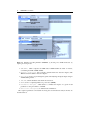
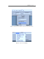
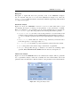
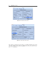
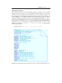
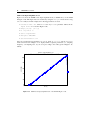
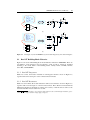
SIMSIDES
User Guide
José M. de la Rosa and Rocı́o del Rı́o
Institute of Microelectronics of Seville, IMSE-CNM
(CSIC/University of Seville)
E-mail: [jrosa,rocio]@imse-cnm.csic.es
Version 2.0, April 2013
CONTENTS
1
SIMSIDES User Guide
1.1 Getting Started: Installing and Running SIMSIDES
1.2 Building and Editing Σ∆M Architectures in SIMSIDES
1.3 Analyzing Σ∆Ms in SIMSIDES
1.4 Example
1.5 Getting Help
1
1
2
2
13
20
2
SIMSIDES Block Libraries and Models
2.1 Overview of SIMSIDES Libraries
2.2 Real SC Building-Block Libraries
2.2.1 Real SC Integrators
2.2.2 Real SC Resonators
2.2.3 Real CT Integrators
2.3 Real CT Building-Block Libraries
2.3.1 Real CT Resonators
2.4 Real Quantizers & Comparators
2.5 Real D/A Converters
2.6 Auxiliary Blocks
23
23
23
23
24
27
27
27
28
34
34
1
SIMSIDES User Guide
SIMSIDES (SIMulink-based SIgma-DElta Simulator) is a time-domain behavioral simulator
for Σ∆Ms that has been developed as a toolbox in the MATLAB/SIMULINK environment.
SIMSIDES can be used for simulating any arbitrary Σ∆M architecture, implemented with
both DT and CT circuit techniques. To this end, a complete list of Σ∆M building blocks
(integrators, resonators, quantizers, embedded DACs, etc) is included in the toolboox.
The behavioral models of these building blocks take into account the most critical error
mechanisms of different circuit techniques including SC, SI, and CT circuits. These models,
validated through transistor-level electrical simulations and by experimental measurements
taken from a number of silicon prototypes, have been incorporated into the SIMULINK
environment as C-MEX S-functions. This approach drastically increases the computational
efficiency in terms of CPU time and accuracy of the simulation results.
The behavioral models included in SIMSIDES have been compiled and tested in a
number of operating systems, including Apple OS X, UNIX (Solaris), Linux, and Microsoft
Windows. Both 32-bit and 64-bit system platforms have been successfully tested in the
majority of them.
Although SIMSIDES was originally developed using MATLAB 6.5 and SIMULINK 5,
the toolbox has been updated and successfully used in a number of MATLAB/SIMULINK
versions in the last years. This appendix provides a user guide of SIMSIDES, giving an
overview of the most significant features of the simulator.
1.1
Getting Started: Installing and Running SIMSIDES
A free copy of SIMSIDES can be downloaded from the following web site:
http://www.imse-cnm.csic.es/simsides
After completing the online registration form and accepting the terms and conditions for
using SIMSIDES, a zip file named simsides.zip is downloaded. The following steps must
be followed to install the toolbox:
1. Uncompress the simsides.zip file to a directory of your computer hard disk. Let us
assume that the directory is named SIMSIDES .
2. Start MATLAB program.
3. Set the MATLAB search path in order to add the SIMSIDES directory. To do this,
go to File menu in MATLAB and select Set Path. The Set Path dialog box
Extracted from the book ”CMOS Sigma-Delta Converters: Practical Design Guide,” José M. de la Rosa and Rocı́o del Rı́o
c 2013 John Wiley & Sons, Ltd. Published 2013 by John Wiley & Sons, Ltd.
2
SIMSIDES User Guide
opens, listing all folders on the search path. From this dialog box, click the button
Add with Subfolders and select the SIMSIDES directory to add to the search
path. In order to reuse the newly modified search path including SIMSIDES directory
and subdirectories, click Save, and finally click Close. This procedure–illustrated in
Figure 1.1a–must be done only the first time SIMSIDES is installed in the hard disk.
In order to start SIMSIDES, type simsides at the MATLAB prompt and the SIMSIDES
main window is displayed, as illustrated in Figure 1.1b.
1.2
Building and Editing Σ∆M Architectures in SIMSIDES
To create a new Σ∆M architecture in SIMSIDES, select File and then New Architecture
in the main menu, and a new SIMULINK model window is displayed. Alternatively, an
existing Σ∆M architecture can be opened by selecting File -> Open Architecture as
illustrated in Figure 1.2.
In order to define a Σ∆M block diagram in SIMSIDES, the required building blocks
can be incorporated from the Edit menu as shown in Figure 1.3. Both SIMULINK and
SIMSIDES library models can be included by selecting Edit -> SIMULINK Library or
Edit -> Add block , respectively. The latter option allows users to browse through all
SIMSIDES library models. This way, clicking on Edit -> Add blocka new window is
displayed where the user can select either ideal or real building blocks, by choosing either
Add Ideal Block or Add Real Block menus, respectively. In both cases, building-block
models are organized in a set of sublibraries, namely: integrators, quantizers & comparators,
D/A converters, resonators, and auxiliary blocks. The latter are only available in real libraries.
Some model libraries are grouped in sublibraries that contain different models
corresponding to different kinds of circuit implementations. For instance, if library
Real Integrators is selected, a new window is displayed where the user can select the
circuit technique (CT, SC, or SI) as well as the type of integrator (i.e., either FE or LD in
the case of SC and SI integrators, and Gm-C, Gm-MC, active-RC, MOSFET-C in the case
of CT integrators). As an illustration, Figure 1.3 shows different sublibraries contained in the
Real Integrators library. A complete list of model libraries and sublibraries is given in
Chapter 2 of this user guide.
Once the Σ∆M block diagram is completed and the different building-block model
parameters have been defined in the MATLAB workspace, the modulator can be simulated
in SIMULINK following the same procedure as for the simulation of an arbitrary model
in SIMULINK; i.e., choosing Simulation -> Start menu in the SIMULINK model
window.
1.3
Analyzing Σ∆Ms in SIMSIDES
Simulation output data can be post-processed in SIMULINK using the Analysis menu. As
illustrated in Figure 1.4, the Analysis menu includes the following submenus:
• Node Spectrum Analysis, which computes and plots the FFT magnitude spectrum
of a given signal.
• Integrated Power Noise, used for calculating and graphically representing the
IBN within a given signal bandwidth.
SIMSIDES User Guide
3
(a)
(b)
Figure 1.1 Installing and starting SIMSIDES: (a) Setting the MATLAB path. (b) Starting SIMSIDES
at the MATLAB prompt.
4
SIMSIDES User Guide
(a)
(b)
Figure 1.2 Building and editing Σ∆Ms in SIMSIDES: (a) Creating a new Σ∆M architecture. (b)
Opening an existing model.
• SNR/SNDR , which computes the SNR and/or SNDR within the band of interest,
considering both LP- and BP-Σ∆Ms.
• Harmonic Distortion, that computes dynamic harmonic distortion figures, like
THD and intermodulation distortion figures.
• Histogram, used for representing histograms and analyzing the input/output swing in
Σ∆M building blocks.
• INL/DNL, which calculates static harmonic distortion.
• MTPR, used for computing multi-tone power ratio (MTPR).
• Parametric Analysis , which allows to simulate the impact of a given model
parameter on the performance of Σ∆Ms.
• Monte Carlo Analysis, to do Monte Carlo simulations.
The required parameters and details involving the aforementioned analysis menus are
described below.
SIMSIDES User Guide
Figure 1.3 Illustrating different sublibraries included in the Real Integrators library.
Figure 1.4 Analysis menu in SIMSIDES.
5
6
SIMSIDES User Guide
Node Spectrum Analysis
Figure 1.5a shows the SIMSIDES Node Spectrum Analysis window. The following
parameters are required to compute the FFT magnitude spectrum:
• Name of the signal(s) to process, where different variable names can be
introduced, separated by commas. These variables can be output data generated
in the simulations (for instance, the modulator output data stream), which have
been previously saved in the MATLAB workspace by using the To Workspace
SIMULINK block.
• Sampling frequency; i.e., the sampling frequency in Hz.
• Window, which defines the window function used for computing the FFT. The main
window functions available in MATLAB can be selected, namely: Kaiser, Barlett,
Blackman, Hamming, Hanning, Chebyshev, Boxcar, and Triangular.
• Number of Points; i.e., the number of points (N in Figure 1.5) for the selected
window function and for FFT computation.
• Window Parameters, where other parameters required to define the window function
are defined (like Beta parameter used in Kaiser windows).
Once these parameters have been defined, the output spectrum can be computed by clicking
on the Compute button and then selecting the signal to be processed from the new window
that is displayed (Signal Spectrum window shown in Figure 1.5b).
Integrated Power Noise
Figure 1.6 shows the SIMSIDES Integrated Power Node window used for computing
the IBN of any arbitrary data sequence obtained from simulations. To compute IBN, the
following parameters are required:
(a)
Figure 1.5
(b)
Node spectrum analysis menu.
SIMSIDES User Guide
7
Figure 1.6 Integrated power noise menu.
• Name of the signal(s) to process.
• Sampling frequency; i.e., the sampling frequency in Hz.
• Oversampling ratio; i.e., the value of OSR that defines the signal bandwidth in
which the IBN is computed.
• Input frequency, where it is assumed that a single-tone input signal is applied.
• Window Parameters; i.e., the parameters required to defined the window function
used for computing the IBN.
• Kind of Spectrum, which specifies the signal nature; i.e., low-pass (LP) or bandpass (BP).
After defining all parameters described above, the IBN is computed by clicking
on the Compute button. Harmonic distortion can be also taken into account in the
calculation of the IBN by clicking the Include Harmonic in Noise Power button.
The signal spectrum can be also plotted together with the IBN by choosing the
Include Signal Spectrum option.
SNR/SNDR
Figure 1.7 shows the SIMSIDES SNR/SNDR window. The parameters required to calculate
the SNR/SNDR of a given signal are essentially the same as those used for computing IBN–
described in the previous section. In this case either the SNR or the SNDR is computed
8
SIMSIDES User Guide
depending on the Figure of merit selected. Note that this kind of analysis calculates the
SNR/SNDR for a given value of the input signal amplitude. If a SNR-versus-amplitude curve
is required, a parametric analysis should be chosen as will be described later.
Harmonic Distortion
Figure 1.8 shows the SIMSIDES Harmonic Distortion window, which is used for
computing the harmonic distortion power. Two different figures of merit can be calculated,
namely: THD and third-order intermodulation distortion (IM3 in Figure 1.8). The latter
requires using a two-tone input signal. For that reason, there is an additional parameter named
Input2 Frequency that defines the frequency of the second input tone.
Integral and Differential Non-Linearity
The INTEGRAL AND DIFFERENTIAL NON-LINEARITY menu, illustrated in Figure 1.9, is
used for characterizing the static linearity in SIMSIDES. The analysis is based on either
Histograms or Input Ramp Waveform–selected by the user. Other parameters required
to do this analysis are the Input Amplitude and the Number of bits, which specifies
the ideal resolution of the A/D conversion, expressed in bits.
Figure 1.7 SNR/SNDR menu.
SIMSIDES User Guide
Figure 1.8 Harmonic distortion analysis menu.
Figure 1.9 Integral and differential non-linearity analysis menu.
9
10
SIMSIDES User Guide
Multi-Tone Power Ratio
SIMSIDES can also analyze the harmonic distortion in those telecom applications such as
ADSL, where a discrete multi-tone (DMT) signal is used. In this case, the linearity of the
system is measured by a figure named multi-tone power ratio (MTPR). The corresponding
SIMSIDES menu–shown in Figure 1.10–allows to compute MTPR for DMT input signals of
different types:
• Supressing 1 carrier of each 16; i.e., 1 out of 16 carrier channels are
suppressed.
• Supressing 8 carrier of each 128; i.e., 8 out of 128 carrier channels are
suppressed.
• Supressing 16 carrier of each 256; i.e., 16 out of 256 carrier channels are
suppressed.
In addition, the following parameters are also needed to compute MTPR:
• Number of carriers, which stands for the number of carrier channels in which the
DMT signal is divided.
• Bins by carrier; i.e., the number of bins assigned to each carrier channel in the
FFT.
Figure 1.10 Multi-tone power ratio analysis menu.
SIMSIDES User Guide
11
Histogram
Histograms of signals that have been previously saved on the MATLAB workspace
can be computed using the HISTOGRAM menu (illustrated in Figure 1.11), where the
Number of bins specifies the number of intervals in which the signal range will be divided
to compute the histogram.
Parametric Analysis
Figure 1.12 shows the SIMSIDES PARAMETRIC ANALYSIS menu. This menu is used
for analyzing the impact of varying a model parameter on the performance of Σ∆Ms.
Either one parameter or two parameters can be varied simultaneously by selecting the
Second Parameter option. For each parameter, the following data must be specified:
• Parameter Name; i.e., the name of the model parameter to be varied. This model
parameter can be a variable used in a Σ∆M building block model (like for instance Io ,
gm , etc) or a simulation parameter, like the input signal amplitude, sampling frequency,
etc.
• Range [vi,vf], which defines the variation range, defined by an interval with a
lower value given by vi and a upper value of vf.
• N. of points; i.e., the number of points in which the variation interval is divided.
• Scale, that specifies if the variation range is either linear or logarithmic.
• Analysis, that specifies the type of analysis to be carried out, including output
spectrum, IBN, SNR/SNDR, INL, MTPR, harmonic distortion, histograms, etc.
Monte Carlo Analysis
Figure 1.13 shows the SIMSIDES menu to run a Monte Carlo analysis. This is a particular
case of parametric analysis, which has essentially the same functionalities and model
parameters. The only difference is that the variation of the parameters involved in the Monte
Figure 1.11 Histogram analysis menu.
12
SIMSIDES User Guide
Figure 1.12 Parametric analysis menu.
Figure 1.13 Monte Carlo analysis menu.
Carlo analysis are randomly varied according to a probability distribution with a mean
value and a standard deviation which are specified in the analysis menu. Different types
of probability distributions can be chosen, including Normal, Log-Normal, Exponential,
and Uniform distributions.
13
SIMSIDES User Guide
1.4
Example
This section illustrates the use of SIMSIDES through a simple example in which several kinds
of analysis will be carried out to show the main features of the toolbox. Figure 1.14 shows
the block diagram of the modulator under study, which consists of a third-order cascade 2-1
DT-Σ∆M with single-bit quantization in both stages.
Creating the Cascade 2-1 Σ∆M Block Diagram in SIMSIDES
The modulator block diagram shown in Figure 1.14 can be implemented by using the model
libraries available in SIMSIDES. To this end, the same procedure as described in Section 1.2
is followed:
• Go to SIMSIDES main menu, select File -> New Architecture and introduce a
name for the new Σ∆M architecture.
• Include the integrators and comparators from the SIMSIDES model libraries. To do
this, select Edit -> Add Block. In this example, the FE integrators in Figure 1.14
are implemented by using the SC_FE_Integrator_All_Effects blocks from
the Real Integrators library, whereas single-bit quantizers are modeled
by the Real_Comparator_Offset&Hysteresis comparator block available in
Quantizers&Comparators library. These building blocks can be incorporated
in the new architecture by simply dragging and dropping the models from their
corresponding SIMSIDES libraries, as illustrated in Figure 1.15a.
• Incorporate the remaining building blocks from the SIMULINK model library. To
do this, go to Edit -> Simulink Library and drag the required models. In this
example the following blocks are required: Sine Wave and Ground blocks from
Sources library, Unit Delay and Discrete Filter block from the Discrete
library, and To Workspace from Sinks library.
• Finally, once all required blocks have been included in the new architecture, they
are properly connected to implement the required Σ∆M architecture shown in
Figure 1.15b.
x
0.25
+
-
!
z −1
1 − z −1
1
+!
-
z −1
1 − z −1
z −1
+
0.5
0.25
+
1
0.5
+!
-
z −1
1 − z −1
2
+
+
!
(1 − z −1 )2
0.5
Digital Cancellation Logic
Figure 1.14 Z-domain block diagram of a cascade 2-1 DT-Σ∆M.
!
y
14
SIMSIDES User Guide
Sine Wave
Block
To Workspace
Block
Ground
Block
(a)
(b)
Figure 1.15 SIMSIDES block diagram of the Σ∆M shown in Figure 1.14: (a) Building and editing
the block diagram. (b) Complete modulator block diagram in SIMSIDES.
SIMSIDES User Guide
15
Setting Model Parameters
The modulator parameters and model parameters required to simulate the block diagram
of Figure 1.15 can be either set up in the MATLAB command window or they can be
alternatively saved in an M-file that is loaded when needed. As an illustration, Figure 1.16
shows the M-file used for setting up all model parameters of Figure 1.15, that also includes
a brief description of the different parameters and variables included. For the sake of
completeness, Table 1.1 includes the values of all building-block parameters as they are
described in the SIMSIDES user masks, as well as other auxiliary block parameters (such as
those used in Sine Wave and To Workspace blocks) which are required during simulation.
In addition to these model parameters, simulation parameters must be set up to run a
simulation. To do this, go to Simulation -> Simulation Parameters menu and define
the following parameters:
• Simulation Time: Start Time: 0.0 ; Stop Time: (N-1)*Ts
% SDM parameters:
% Sampling Frequency(fs), Input Frequency (fi), Sampling Time (Ts)
% OverSampling Ratio (OSR=M); Number of points (N)
fs=5.12e6; fi=5e3; Ts=1/fs; M=128; N=65536;
% Model parameters
kt=0.026*1.6e-19; % Boltzmann constant
% First Integrator's parameters
Cint1=24e-12; % integration capacitor For gain=1
Cs11=6e-12; % sampling capacitor (branch 1)
Cs21=6e-12; % sampling capacitor (branch 2)
innoise1=0; % rms value of the input equivalent noise
ao1=2.63e3; % open-loop OTA DC gain
gm1=4.5e-3; % transconductance
io1=0.977e-3; % maximum OTA output current
ron1=60; % sampling switch-on resistance
% Second- and Third- Integrators
Cint2=3e-12;
Cs12=1.5e-12;
Cs22=1.5e-12;
innoise2=0;
ao2=1.38e3;
gm2=0.87e-3;
io2=0.25e-3;
ron2=650;
% Common integrator parameters
temp=175; % temperature
osp=2.7; % output swing
cnl1=0; % capacitor first-order non-linear coef.
cnl2=25e-6; % capacitor second-order non-linear coef.
avnl1=0; % DC gain first-order non-linear coef.
avnl2=15e-2; % DC gain second-order non-linear coef.
avnl3=0; % DC gain third-order non-linear coef.
avnl4=0; % DC gain fourth-order non-linear coef.
cpar1=0.6e-12; % parasitic (opamp) input capacitance
cpar2=0.6e-12;
cload=2.28e-12; % opamp (intrinsic) load capacitance
% Comparators
vref=2; % DAC reference voltage
hys=30e-3; % comparator hysteresis
Figure 1.16
M-file including all model parameters required to simulate the Σ∆M in Figure 1.15b.
16
SIMSIDES User Guide
Table 1.1
Building-block model parameters used for simulating the Σ∆M in Figure 1.15b.
Building Block
Parameter Description
Value/Variable
Input Sine Wave
Sine Type
Amplitude
Bias
Frequency (rad/s)
Phase (rad)
Sample time
Interpret vector parameters
Time based
0.5
0
2*pi*fi
0
0
Selected
First Integrator
Integration and Sampling Capacitors (Branch 1, Branch 2)
Capacitor nonlinear coefficients
Weight’s variance, rms eq.input noise, temperature
OTA DC gain, transconductance, max. output current
Positive/Negative Output swing
Switch on-resistance
OTA DC gain nonlinear coefs.
Parasitic capacitances before the OTA
Load capacitance
Positive Input 1 is sampled at...
Sampling Time
Identifier for this integrator
Identifier for the next integrator
[Cint1,Cs11,Cs21]
[cnl1,cnl2]
[0,innoise1,temp]
[ao1,gm1,io1]
[osp,-osp]
ron1
[avnl1,2,3,4]
[cpar1,cpar2]
cload
phi1
Ts
a
b
Second, Third
Integrators
Integration and Sampling Capacitors (Branch 1, Branch 2)
Capacitor nonlinear coefficients
Weight’s variance, rms eq.input noise, temperature
OTA DC gain, transconductance, max. output current
Positive/Negative Output swing
Switch on-resistance
OTA DC gain nonlinear coefs.
Parasitic capacitances before the OTA
Load capacitance
Positive Input 1 is sampled at...
Sampling Time
Identifier for this integrator (second integrator)
Identifier for this integrator (third integrator)
Identifier for the next integrator
[Cint2,Cs12,Cs22]
[cnl1,cnl2]
[0,innoise2,temp]
[ao2,gm2,io2]
[osp,-osp]
ron2
[avnl1,2,3,4]
[cpar1,cpar2]
cload
phi1
Ts
b
c
c
Comparators
Vhigh, Vlow
Offset, Hysteresis
Phase ON
Sampling Time
Identifier for this quantizer
[vref, -vref]
[0,hys]
phi1
Ts
quant1
To Workspace (y)
Variable name
Limit data points to last
Decimation
Sample Time
Save format
y
N
1
Ts
Array
SIMSIDES User Guide
17
• Solver options: Type: Variable Step ; Max Step Size: Auto
Note that integrator building blocks are identified in order to properly compute the
equivalent load capacitances required for the incomplete settling error model.
Computing Output Spectrum
The output spectrum of the Σ∆M can be computed in SIMSIDES by following the next
steps:
• Set up model parameters by using the M-file shown in Figure 1.16.
• Simulate the modulator in Figure 1.15b from the menu Simulation -> Start.
• Once the simulation has finished, go to Analysis -> Node Spectrum Analysis
menu in SIMSIDES.
• Define the parameters requested in that menu. In this example, the sampling frequency
is defined as fs and a Kaiser window function is used with a number of points N and
Beta = 20.
• Click on Compute and then Plot, and the output spectrum shown in Figure 1.17 is
displayed.
Modulator Output (Magnitude) Spectrum
0
−20
Magnitude (dB)
−40
−60
−80
−100
−120
−140
−160 1
10
2
10
3
10
4
10
Frequency (Hz)
5
10
6
10
Figure 1.17 Output spectrum (magnitude) of the Σ∆M in Figure 1.15b.
18
SIMSIDES User Guide
SNR versus Input Amplitude Level
Figure 1.18 shows the SNDR versus input amplitude level (or SNDR curve) of the Σ∆M
in Figure 1.15b. This figure has been obtained by using the Analysis menu and choosing
SNR/SNDR analysis. In this example, the following parameters are used:
• Parameter Name: Ain, where Ain is the Amplitude parameter defined in the
Input Sine Wave block in Figure 1.15b.
• Range [vi,vf]: [1e-6,2]
• N. of points: 50
• Scale: Logarithmic
• Analysis: SNR/SNDR
• Second Parameter: Off
Once the aforementioned parameters are set up, click on Continue and the SNR/SNDR
window menu shown in Figure 1.7 is displayed. The requested parameters (i.e., sampling
frequency, oversampling ratio, etc) are set up according to the values given in Figure 1.16,
namely:
SNDR vs. Input Amplitude Level
100
SNDR (dB)
80
60
40
20
0 −6
10
−5
10
−4
10
−3
10
Ain (V)
−2
10
−1
10
0
10
Figure 1.18 SNDR versus input amplitude level of the Σ∆M in Figure 1.15b.
SIMSIDES User Guide
19
• Name of the signal(s) to process: y
• Sampling frequency (Hz): fs
• Oversampling ratio: M
• Input Frequency (Hz): fi
• Window: Kaiser
• N. of Points: N
• Beta: 20
• Kind of Spectrum: LP
• Figure of merit: SNDR
After setting up the aforementioned parameters, click on Compute and then Plot to obtain
the curve given in Figure 1.18.
Parametric Analysis Considering Only One Parameter
The Parametric Analysis menu can be used for studying the effect of a given model
parameter on the modulator performance. For instance, let us consider the effect of
the OTA transconductance gm of the front-end integrator in Figure 1.15b. In order to
analyze the impact of this parameter on the effective resolution of the modulator, go to
Parametric Analysis menu and set up the following parameters:
• Parameter name: gm1, which stands for gm of the front-end integrator block in
Figure 1.15b.
• Range [vi,vf]: [1e-5,1e-3]
• N. of points: 50
• Scale: Linear
• Analysis: SNR/SNDR
• Second Parameter: Off
Once these parameters are defined, click on Continue and proceed in a similar way to
previous examples in order to compute the SNDR. Figure 1.19 shows the results of this
analysis, by depicting the SNDR versus gm1.
Parametric Analysis Considering Two Parameters
The Parametric Analysis menu can be used also for implementing parametric analyses
considering the variation of two different parameters. As an example, Figure 1.20 shows the
effect of both the OTA transconductance gm1 and the maximum output current Io1 of the
front-end amplifier on the SNDR of the Σ∆M in Figure 1.15b.
In order to obtain the graph in Figure 1.20, the following parameters are set up in the
Parametric Analysis menu:
• Parameter name: io1, which stands for the maximum output current Io of the
front-end integrator.
20
SIMSIDES User Guide
SNDR vs. gm1
110
100
90
SNDR (dB)
80
70
60
50
40
30
0
0.1
0.2
0.3
0.4
0.5
gm1 (A/V)
0.6
0.7
0.8
0.9
1
−3
x 10
Figure 1.19 Using parametric analysis to study the effect of a single model parameter: SNDR versus
transconductance of the front-end amplifier for the Σ∆M in Figure 1.15b.
• Range [vi,vf]: [1e-4,1e-3]
• N. of points: 10
Computing Histograms
Finally, to conclude this example, Figure 1.21 illustrates the histograms of the integrators
outputs in the front-end stage of the modulator in Figure 1.15b.
These histograms have been obtained by using the Analysis -> Histograms menu
from SIMSIDES and setting up the following model parameters:
• Name of the signal(s) to process: y1,y2, which are the names given to the
output of the integrators saved into the MATLAB workspace by using To Workspace
blocks from the SIMULINK elementary library.
• Number of bins: 100
1.5
Getting Help
SIMSIDES includes a help menu (illustrated in Figure 1.22) from which this user guide
can be opened by selecting Help -> User Manual in the SIMSIDES main window. In
addition, a complete list of all behavioral models (and their corresponding parameters)
included in SIMSIDES–described in Appendix 2–can be also obtained from this menu by
selecting Help -> Libraries and Models.
SIMSIDES User Guide
21
SNDR vs. gm1, io1
110
100
90
SNDR (dB)
80
70
60
50
40
30
20
10
1
0.8
1
0.6
0.8
0.6
0.4
−3
x 10
0.4
0.2
io1 (A)
−3
x 10
0.2
0
0
gm1 (A/V)
Figure 1.20 Parametric analysis considering the effect of two parameters (gm1 and Io1 ) on the SNDR.
SIMSIDES User Guide
Histogram of the First Integrator Output
2500
Number of Events
2000
1500
1000
500
0
−1.5
−1
−0.5
0
Signal Amplitude
0.5
1
1.5
Histogram of the Second Integrator Output
1200
1000
Number of Events
22
800
600
400
200
0
−2
−1.5
−1
−0.5
0
Signal Amplitude
0.5
1
1.5
2
Figure 1.21 Illustrating the use of histograms of the modulator in Figure 1.15b.
Figure 1.22 Help menu.
2
SIMSIDES Block Libraries and
Models
2.1
Overview of SIMSIDES Libraries
Table 2.1 compiles all libraries included in SIMSIDES together with a brief description of
their contents. These libraries are divided into two main categories: ideal libraries and real
libraries. The former contains ideal building blocks, whereas the latter includes behavioral
models that incorporate circuit-level nonidealities. The libraries containing integrators and
resonators are subdivided into several specific sublibraries, which include in turn buildingblock models corresponding to different circuit-level implementations. For instance, SC
integrators are subdivided into FE and LD integrators; CT integrators are subdivided into
Gm-C, active-RC, etc.
2.2
Real SC Building-Block Libraries
SIMSIDES includes two libraries of SC integrators and two libraries of SC resonators. These
libraries are described below.
2.2.1
Real SC Integrators
There are two SC integrator model libraries in SIMSIDES: one including FE SC integrator
models and the other one including LD SC integrators. In both cases, integrator models are
classified according to the nonideal effects that are included in the model and the number
of SC branches connected at the integrator input. This way, for each model there are four
building blocks using the same behavioral model except for the number of input SC branches.
As an illustration, Figure 2.1 shows the symbol used in SIMSIDES for one-branch SC FE
integrators (Figure 2.1a) and two-branch SC FE integrators (Figure 2.1b), together with their
equivalent SC circuits. Note that, although single-ended conceptual schematics are shown in
this figure, fully-differential circuits are assumed in the behavioral models.
Both integrators in Figure 2.1 use the same behavioral model, which consists of an ideal
SC FE integrator with output swing limitation. The behavioral model corresponding to a
one-branch SC FE integrator is named Basic_SC_FE_Int, while the model of the twobranch SC FE integrator is named Basic_SC_FE_IntII. Following this nomenclature,
Basic_SC_FE_IntIII and Basic_SC_FE_IntIV models are used for three- and fourbranch SC FE integrators, respectively.
Extracted from the book ”CMOS Sigma-Delta Converters: Practical Design Guide,” José M. de la Rosa and Rocı́o del Rı́o
c 2013 John Wiley & Sons, Ltd. Published 2013 by John Wiley & Sons, Ltd.
24
SIMSIDES Block Libraries and Models
Table 2.1
Overview of SIMSIDES libraries.
Ideal Libraries
Sublibraries
Building Blocks
Integrators
Resonators
Quantizers & Comparators
D/A Converters
–
–
–
–
Ideal DT/CT integrators
Ideal resonators
Ideal quantizers
Ideal DACs
Real Libraries
Sublibraries
Building Blocks
Integrators
SC FE integrators
SC LD integrators
SI FE integrators
SI LD integrators
gm-C integrators
gm-MC integrators
RC integrators
MOSFET-C integrators
Forward-Euler SC integrators
Lossless-Direct SC integrators
Forward-Euler SI integrators
Lossless-Direct SI integrators
Gm-C integrators
Miller OTA integrators
Active-RC integrators
MOSFET-C integrators
Resonators
SC FE resonators
SC LD resonators
SI FE resonators
SI LD resonators
gm-C resonators
gm-LC resonators
Resonators based on FE SC integrators
Resonators based on LD SC integratorss
Resonators based on FE SI integrators
Resonators based on LD SI integrators
Resonators based on Gm-C integrators
Resonators based on Gm-LC integrators
Quantizers & Comparators
–
Nonideal single-bit & multibit quantizers
D/A Converters
–
Nonideal single-bit and multibit DACs
Auxiliary Blocks
–
Adders, latches, DEM blocks, etc
Table 2.2 lists all SC integrator models available in SIMSIDES including a brief
description of the nonidealities included in each of them. Note that the model names
included in Table 2.2 correspond to one-branch integrators. The same models are available
for integrators with up to four input branches.
Table 2.3 lists the most important parameters used by the SC integrator behavioral models
in SIMSIDES, as well as a brief description of all of them.
2.2.2
Real SC Resonators
SIMSIDES has two SC resonator model libraries corresponding to FEI-based resonators and
LDI-based resonators. Following the same philosophy as that used in SC integrators, the
behavioral models of SC resonators in SIMSIDES are classified attending to the number of
input SC branches and the circuit nonideal effects included in the models.
Table 2.4 lists all SC resonator models available in SIMSIDES, including a brief
description of the nonidealities considered in each of them. The parameters used in these
models are the same as those included in SC integrator models–listed in Table 2.3. In addition
to these parameters, the resonator gain can also be defined by the user by setting a parameter
named Gain ,which can be defined in the model dialogue box.
SIMSIDES Block Libraries and Models
Table 2.2
25
Library of SC (FE/LD) integrators included in SIMSIDES.
Model name
Circuit effects included
Basic_SC_FE_Int
Basic_SC_LD_Int
Output swing limitation
SC_FE_Int_Non_linear_C
SC_LD_Int_Non_linear_C
Output swing limitation,
capacitor nonlinearity.
SC_FE_Int_Weight_Mismatch
SC_LD_Int_Weight_Mismatch
Output swing limitation,
capacitor mismatch.
SC_FE_Int_Non_Linear_Sampling
SC_LD_Int_Non_Linear_Sampling
Output swing limitation,
nonlinear switch on-resistance.
SC_FE_Int_FiniteDCgain
SC_LD_Int_FiniteDCgain
Finite OTA DC gain,
output swing limitation,
parasitic OTA caps.
SC_FE_Int_Finite&Non_LinearDCGain
SC_LD_Int_Finite&Non_LinearDCGain
Finite nonlinear OTA DC gain,
output swing limitation
parasitic OTA caps.
SC_FE_Int_Noise
SC_LD_Int_Noise
OTA thermal noise, output swing
limitation, parasitic/load OTA caps.
SC_FE_Int_Settling
SC_LD_Int_Settling
Incomplete settling error, output swing
limitation, parasitic/load OTA caps.
SC_FE_Integrator_All_Effects
SC_LD_Integrator_All_Effects
switch on-resistance,
capacitor nonlinearity and mismatch,
settling error, finite (nonlinear) DC gain,
thermal noise, parasitic/load capacitors,
output swing limitation.
SC_FE_Integrator_All_Effects&NonLinSamp
SC_LD_Integrator_All_Effects&NonLinSamp
switch nonlinear on-resistance,
capacitor nonlinearity and mismatch,
settling error, finite (nonlinear) DC gain,
thermal noise, parasitic/load capacitors,
output swing limitation.
SC_FE_Int_1b_SD2
switch on-resistance and its effect on
GB and SR,
capacitor nonlinearity and mismatch,
settling error, finite (nonlinear) DC gain,
thermal noise, parasitic/load capacitors,
output swing limitation.
SC_FE_Int_1b_DEM_SD2
switch on-resistance and its effect on
GB and SR,
array of unit sampling capacitors,
capacitor nonlinearity and mismatch,
settling error, finite (nonlinear) DC gain,
thermal noise, parasitic/load capacitors,
output swing limitation.
26
SIMSIDES Block Libraries and Models
Table 2.3
Model parameters used in SIMSIDES SC (FE/LD) integrators.
Parameter name (in alphabetical order)
Brief description
Array of sampling capacitors
for DEM branch
Array of unit capacitors
used with multilevel DACs with DEM
B (switch parameters)
MOS large-signal transconductance
(analytic model)
Bandwidth (BW)
Input signal bandwidth
Capacitor (first/second)-order
nonlinearity
Capacitor (first/second)
order nonlinearity
Finite and Linear Ron
switch on-resistance, linear model
Finite DC Gain of the AO
Finite OTA DC gain
g (switch parameters)
Finite switch on-conductance
(analytic model)
Identifier for this integrator
Identifier used for settling error model
Input Equivalent Thermal Noise
OTA input-referred thermal noise
Input parameters [A,fi,ph] (switch)
Amplitude, frequency, and phase of
the sinewave input
(table look-up model)
Integration/Sampling Capacitor
Integration/sampling capacitors
Integration additional load
Additional load capacitance
at the integration phase
Load Capacitor (cload)
Integrator load capacitance
Maximum output current (Io)
OTA maximum output current
Nonlinearity of the DC Gain
OTA DC gain nonlinear coefficients
Output Swing Up/Down
Maximum/minimum output swing limits
Parasitic Capacitor before the AO (Cp)
Parasitic capacitance at the OTA input
pcoef (switch parameters)
nonlinear coefficients of
the switch on-resistance
(table look-up model)
Positive Input is Sampled in...
Input-switch clock phase
Ron
switch on-resistance
Sampling additional load
Additional load capacitance
at the sampling phase
Sampling Time
Clock signal period
Switch on-resistance (Ron)
Switch on-resistance
Temp
Temperature (K)
Transconductance of the AO (gm)
OTA transconductance
Variance
Variance of the capacitor mismatch error
SIMSIDES Block Libraries and Models
27
CI
CS1
v+
v+
v-
+
-
!
v-
φ1
φ2
φ2
φ1
+
vo
vo
(a)
CI
CS1
v1+
v1-
φ1
φ2
φ2
φ1
+
vo
CS2
v1+
v1-
+1
-1
v2+
v2-
+2
-2
!
v2+
v2-
vo
φ1
φ2
φ1
(b)
Figure 2.1 SC integrator symbol in SIMSIDES: (a) One-branch integrator. (b) Two-branch integrator.
2.3
Real CT Building-Block Libraries
Figure 2.2 shows the CT building-block model libraries included in SIMSIDES. There are
four libraries of CT integrators and two libraries of CT resonators, which are classified
attending to the circuit nature of the building blocks, namely: Gm-C, Gm-MC, Gm-LC,
active-RC, and MOSFET-C.
2.3.1
Real CT Integrators
Tables 2.5–2.8 list all models1 included in CT integrator libraries shown in Figure 2.2,
together with a brief description of the nonideal effects included.
2.3.2
Real CT Resonators
Tables 2.9 and 2.10 list all models included in CT resonator libraries shown in Figure 2.2,
together with a brief description of their nonideal effects. These libraries include different
building blocks that are classified according to the accuracy of their models as well as to the
circuit nonidealities that are taken into account.
1 RC Int 1,2,3in models allow to set up transistor-level parameters such as channel-length modulation, gate-tosource overdrive voltage, saturation voltage, supply voltage, etc.
28
SIMSIDES Block Libraries and Models
Table 2.4 Library of SC (FE/LD) resonators included in SIMSIDES.
2.4
Model name
Circuit effects included
Basic_SC_FE_Res
Basic_SC_LD_Res
Output swing limitation
SC_FE_Res_NonLinear_C
SC_LD_Res_NonLinear_C
Output swing limitation,
capacitor nonlinearity.
SC_FE_Res_Weight_Mismatch
SC_LD_Res_Weight_Mismatch
Output swing limitation,
capacitor mismatch.
SC_FE_Res_Non_Linear_Sampling
SC_LD_Res_Non_Linear_Sampling
Output swing limitation,
nonlinear switch on-resistance.
SC_FE_Res_FiniteDCgain
SC_LD_Res_FiniteDCgain
Finite OTA DC gain,
output swing limitation,
parasitic OTA caps.
SC_FE_Res_FiniteDC&NonLinearGain
SC_LD_Res_FiniteDC&NonLinearGain
Finite nonlinear OTA DC gain,
output swing limitation,
parasitic OTA caps.
SC_FE_Res_Noise
SC_LD_Res_Noise
OTA thermal noise, output swing
limitation, parasitic/load OTA caps.
SC_FE_Res_Settling
SC_LD_Res_Settling
Incomplete settling error, output swing
limitation, parasitic/load OTA caps.
SC_FE_Res_All_effects
SC_LD_Res_All_effects
switch on-resistance,
capacitor nonlinearity and mismatch,
settling error, finite (nonlinear) DC gain,
thermal noise, parasitic/load capacitors.
SC_FE_Res_All_effects&NonLinSamp
SC_LD_Res_All_effects&NonLinSamp
switch nonlinear on-resistance,
capacitor nonlinearity and mismatch,
settling error, finite (nonlinear) DC gain,
thermal noise, parasitic/load capacitors,
output swing limitation.
Real Quantizers & Comparators
Table 2.11 lists the building blocks included in the real Quantizers&Comparators SIMSIDES library, together with a brief description of their operation and main circuit nonidealities. In addition to their ideal parameters, additional model parameters are required to model
the different circuit nonidealities. These error parameters are listed in Table 2.12.
Note that, apart from comparators and quantizers, there is a building block named
Real_Sampler, which is used for modeling the S&H circuits that are connected at the
input of embedded quantizers in CT-Σ∆Ms. One of the most critical errors associated to
this building block is the clock jitter, which is modeled as an uncertainty in the sampling
time δt corresponding to a stationary process with zero mean and standard deviation defined
by the user (see Table 2.12).
SIMSIDES Block Libraries and Models
Table 2.5
29
Gm-C integrator library models in SIMSIDES.
Model name
Circuit effects included
Ideal_OTA_C_CTint
Ideal Gm-C integrator.
Transconductor
Input saturation voltage,
nonlinear transconductance.
gm_no_noise_new
Output saturation voltage,
third-order intercept point.
1pole_gm
Gm-C output impedance.
OTA_C_CT_1pole
Input/output saturation voltage,
finite OTA DC gain, nonlinear transconductance,
one-pole dynamic, time-constant error,
nonlinear transconductance, thermal noise.
OTA_C_CT_2poles
OTA_C_CT_2polesb
Input/output saturation voltage,
Finite OTA DC gain, nonlinear transconductance,
two-pole dynamic, time-constant error,
nonlinear transconductance, thermal noise.
Table 2.6 Gm-MC integrator library models in SIMSIDES.
Model name
Circuit effects included
Gm_MC_CTInt_1pole
Input/output saturation voltage,
finite OTA DC gain, parasitic capacitances,
one-pole dynamic, thermal noise.
Gm_MC_CTInt_2poles
Input/output saturation voltage,
finite OTA DC gain, parasitic capacitances,
two-pole dynamic, thermal noise.
Gm...1pole&Large_signal_distortion
Input/output saturation voltage,
output current limit, finite OTA DC gain,
parasitic capacitances, one-pole dynamic.
Gm...2poles&Large_signal_distortion
Input/output saturation voltage,
output current limit, finite OTA DC gain,
parasitic capacitances, two-pole dynamic.
Gm...1pole&Small_Signal_Distortion
Input/output saturation voltage,
output current limit, finite OTA DC gain,
nonlinear transconductance,
parasitic capacitances, one-pole dynamic.
Gm...2poles&Small_Signal_Distortion
Input/output saturation voltage,
output current limit, finite OTA DC gain,
nonlinear transconductance,
parasitic capacitances, two-pole dynamic.
30
SIMSIDES Block Libraries and Models
Table 2.7
Active-RC integrator library models in SIMSIDES.
Model name
Circuit effects included
RC_CTInt_1pole
OTA output swing limitation,
finite OTA DC gain, parasitic capacitances,
capacitance voltage coefficient,
one-pole dynamic, thermal noise.
RC_CTInt_2poles
OTA output swing limitation,
finite OTA DC gain, parasitic capacitances,
capacitance voltage coefficient,
two-pole dynamic, thermal noise.
RC...1pole&Large_signal_distortion
OTA output swing limitation,
output current limit, finite OTA DC gain,
parasitic capacitances,
capacitance voltage coefficient,
one-pole dynamic, thermal noise.
RC...2poles&Large_signal_distortion
OTA output swing limitation,
output current limit, finite OTA DC gain,
parasitic capacitances,
capacitance voltage coefficient,
two-pole dynamic, thermal noise.
RC_Int_1in
RC_Int_2in
RC_Int_3in
OTA output swing limitation,
finite OTA DC gain, nonlinear trans.,
slew rate, parasitic capacitances,
one-pole dynamic, thermal noise.
Table 2.8
MOSFET-C integrator library models in SIMSIDES.
Model name
Circuit effects included
MOSFET_C_CTInt_1pole
OTA output swing limitation,
finite OTA DC gain, parasitic capacitances,
capacitance voltage coefficient,
one-pole dynamic, thermal noise.
MOSFET_C_CTInt_2poles
OTA output swing limitation,
finite OTA DC gain, parasitic capacitances,
capacitance voltage coefficient,
two-pole dynamic, thermal noise.
MOS...1pole&Large_signal_distortion
OTA output swing limitation,
output current limit, finite OTA DC gain,
parasitic capacitances
one-pole dynamic, thermal noise.
MOS...2poles&Large_signal_distortion
OTA output swing limitation,
output current limit, finite OTA DC gain,
parasitic capacitances
two-pole dynamic, thermal noise.
SIMSIDES Block Libraries and Models
Table 2.9 Gm-C resonator library models in SIMSIDES.
Model name
Circuit effects included
Ideal_gmC_CT_Resonator
Ideal Gm-C resonator.
gmC_CT_Res_1pole
Finite OTA DC gain,
time-constant error,
one-pole dynamic, thermal noise.
gmC_CT_Res_2poles
gmC_CT_Res_2polesfull
Finite OTA DC gain,
time-constant error,
two-pole dynamic, thermal noise.
gmC_CT_Res_1pole_larged
Input/output saturation voltage,
output current limit, finite OTA DC gain,
time-constant error, one-pole dynamic.
gmC_CT_Res_2poles_larged
Input/output saturation voltage,
output current limit, finite OTA DC gain,
nonlinear transconductance,
time-constant error, two-pole dynamic.
gmC_CT_Res_1pole_small&larged
Input/output saturation voltage,
output current limit, finite OTA DC gain,
nonlinear transconductance,
time-constant error, one-pole dynamic.
gmC_CT_Res_2poles_small&larged
Input/output saturation voltage,
output current limit, finite OTA DC gain,
nonlinear transconductance,
time-constant error, two-pole dynamic.
31
32
SIMSIDES Block Libraries and Models
Table 2.10 Gm-LC resonator library models in SIMSIDES.
Model name
Circuit effects included
Ideal_gmLC_CT_Resonator
Ideal Gm-LC resonator.
gmLC_CT_Res_1pole
Input/output saturation voltage,
inductance quality factor and series parasitic resistance,
finite OTA DC gain, time-constant error,
one-pole dynamic, thermal noise.
gmLC_CT_Res_2poles
Input/output saturation voltage,
inductance quality factor and series parasitic resistance,
finite OTA DC gain, time-constant error,
two-pole dynamic, thermal noise.
gmLC...1pole_large_dist
Input/output saturation voltage,
inductance quality factor and series parasitic resistance,
output current limitation,
finite OTA DC gain, time-constant error,
one-pole dynamic, thermal noise.
gmLC...2poles_large_dist
Input/output saturation voltage,
inductance quality factor and series parasitic resistance,
output current limitation,
finite OTA DC gain, time-constant error,
two-pole dynamic, thermal noise.
gm...1pole_small&large_dist
Input/output saturation voltage,
inductance quality factor and series parasitic resistance,
output current limitation, nonlinear transconductance,
finite OTA DC gain, time-constant error,
one-pole dynamic, thermal noise.
gmLC...2poles_small&larged
Input/output saturation voltage,
inductance quality factor and series parasitic resistance,
output current limitation, nonlinear transconductance,
finite OTA DC gain, time-constant error,
two-pole dynamic, thermal noise.
SIMSIDES Block Libraries and Models
33
Table 2.11 Real Quantizers and Comparator models included in SIMSIDES.
Model name
Circuit effects included
Real_Comparator_Offset&Hysteresis
Voltage-mode comparator
with offset,
(random & deterministic) hysteresis.
Real_Comparator_Offset&Hysteresis_for_SI
Current-mode comparator
with offset
and nonlinearity (INL).
Real_Multibit_Quantizer
Voltage-mode multibit quantizer
with gain error, offset
(random & deterministic) hysteresis.
Real_Multibit_Quantizer_for_SI
Current-mode multibit quantizer
with gain error, offset, INL,
(random & deterministic) hysteresis.
Real_Multibit_Quantizer_dig_level_SD2
Voltage-mode multilevel quantizer
with gain error, offset, INL,
(random & deterministic) hysteresis.
Real_Sampler
Sampling & Hold circuit with
clock jitter error.
Table 2.12 Error model parameters used in SIMSIDES Real Quantizers.
Parameter name (in alphabetical order)
Brief description
Gain Error in LSB
Gain error measured in LSB.
Jitter typical deviation
Standard deviation of clock jitter error.
Kind of Hysteresis
Comparator hysteresis. It may
be either deterministic or random hysteresis.
INL in LSB
Integral Nonlinearity error measured in LSB.
Number of levels
Number of quantizer levels.
Offset
Offset error.
Offset Error in LSB
Offset error measured in LSB.
Seed for random jitter generation
Seed number used for
generating random jitter error.
34
SIMSIDES Block Libraries and Models
SIMSIDES CT
Building-Block Libraries
Integrators
Resonators
Gm-C
Gm-C
Gm-MC
Gm-LC
MOSFET-C
Active-RC
Figure 2.2 Classification of SIMSIDES CT model libraries.
2.5
Real D/A Converters
Table 2.13 lists the different building blocks included in the real D/A Converters SIMSIDES library, together with a brief description of their operation and main circuit errors.
Error parameters associated to the models listed in Table 2.13 have the same meaning as
those used in multibit quantizers, except for the selectable NRZ/RZ/HRZ DAC waveform and
the delay error. The latter can be chosen to be either a constant delay or a signal-dependent
delay, given by,
d1
delay(vi ) = d0 +
< dmax
(2.1)
x1 · |vi |
where d0, d1, x1, dmax are model parameters set by the user.
2.6
Auxiliary Blocks
In addition to the building blocks described in previous sections, SIMSIDES includes a
library named Auxiliary blocks that contains some other blocks (like adders, DEM
algorithms, and digital latches) also needed to simulate Σ∆Ms. Table 2.14 lists the models
included in the mentioned library together with a brief description of their operation. The
most significant parameters used by these models are listed in Table 2.15.
SIMSIDES Block Libraries and Models
35
Table 2.13 Real DAC models included in SIMSIDES.
Model name
Circuit effects included
Real_DAC_Multibit
Voltage-mode multibit DAC
with offset, gain error, and INL error.
Real_DAC_Multibit_SI
Current-mode multibit DAC
with offset, gain error, and INL error.
Real_DAC_Multibit_delay_Jitter
Voltage-mode multibit DAC
with offset error,
gain error, INL error,
delay error, and clock jitter error.
Real_DAC_Multibit_delay_Jitter_SI
Current-mode multibit DAC
with finite output conductance, offset error,
gain error, INL error,
delay error, and clock jitter error.
Real_DAC_pulse_types
Voltage-mode multibit DAC
with selectable NRZ/RZ/HRZ output waveform.
Real_DAC_Multibit_pulse_types
Voltage-mode multibit DAC
with selectable NRZ/RZ/HRZ output waveform,
gain error, offset error, and INL error.
Real_DAC..._delay_jitter
Voltage-mode multibit DAC
with selectable NRZ/RZ/HRZ output waveform,
gain error, offset error, INL error,
delay error, and clock jitter error.
36
SIMSIDES Block Libraries and Models
Table 2.14 Auxiliary building-block models used in SIMSIDES.
ANALOG ADDERS
Model name
Brief description
Analog_Adder_Ideal_SD2
Ideal SC passive adder with
parasitic input capacitance and load capacitance.
Analog_Adder_real_SD2
Real SC passive adder with
parasitic input capacitance and load capacitance,
switch on-resistance, settling error,
capacitor nonlinearity, and thermal noise.
DIGITAL ADDERS
Model name
Brief description
Dig_add_generic_2outs
Dig_add_3L_5L_13L
Dig_add_3L_3L_5L_2outs
Dig_add_3L_3L_7L_2outs
Dig_add_3L_5L_9L_2outs
Dig_add_3L_5L_13L_2outs
Digital subtraction of a M1 -Level thermometric-coded
signal and a M2 -Level thermometric-coded signal,
which is scaled by a factor of d. The result is a
(M1 + M2 /d)-level thermometric-coded digital output.
DIGITAL LATCHES
Model name
Brief description
D_latch_simplest
D_latch
Digital ”D” latches.
DAC WITH DEM ALGORITHMS
Model name
Brief description
DEM_id_SD2
Ideal DEM algorithm.
DAC - DEM - V04
DAC block with a selectable DEM algorithm.
There are three options: No DEM, DWA, Pseudo-DWA.
Mux_SD2
Building block used for sampling an input (analog) signal
by a number of different branches corresponding
to the number of DAC unit capacitors.
SIMSIDES Block Libraries and Models
Table 2.15 Error model parameters used in SIMSIDES Auxiliary Blocks.
Parameter name (in alphabetical order)
Brief description
Comparator Input Capacitor (C)
Parasitic capacitance at the
comparator/quantizer input.
DEM type
DEM algorithm: (1) No DEM,
(2) DWA, (3) Pseudo-DWA.
(Default = 1)
Input Capacitor (C)
Input capacitance of the analog adder.
Nonlinearities of the capacitors
Capacitance nonlinear coefficients
in an analog adder.
Number of elements
Number of DAC unit elements.
Output type
Digital output code: (1) Binary output,
(2) Trilevel output including common
mode (Default = 1).
Time interval between sampling
and comparison (delta)
Delay between the time instant when
the adding operation is performed
and the time instant when
comparison time takes place.
37