1
The State University of New York (SUNY) at Buffalo
Department of Electrical Engineering
Lab Manual v1.2013
EE 379/578 – Embedded Systems and Applications
Cristinel Ababei
Copyleft © by Cristinel Ababei, 2013. Being a big supporter of open-source, this lab manual is free
to use for educational purposes. However, you should credit the author. The advanced materials
are available for $1, which will be donated to my preferred charity.
Table of Contents
Lab 1: A “Blinky” Introduction to C and Assembly Programming .................................................................... 3
Lab 2: Using UART .......................................................................................................................................... 13
Lab 3: Debugging and More on Interrupts..................................................................................................... 23
Lab 4: CAN and I2C ......................................................................................................................................... 32
Lab 5: USB audio, Stepper Motor .................................................................................................................. 47
Lab 5: Supplemental Material – SPI and SD cards ......................................................................................... 54
Lab 6: Introduction to RTX Real-Time Operating System (RTOS) .................................................................. 66
Lab 7: Introduction to Ethernet ..................................................................................................................... 74
Lab 7: Supplemental Material – AR.Drone Control........................................................................................ 91
Lab 8: Streaming Video from CMOS Camera ................................................................................................. 98
Notes on Using MCB1700 Board.................................................................................................................... 99
2
Lab 1: A “Blinky” Introduction to C and Assembly Programming
1. Objective
The objective of this lab is to give you a “first foot in the door” exposure to the programming in C and
assembly of a program, which when executed by the microcontroller (NXP LPC1768, an ARM Cortex-M3)
simply blinks LEDs located on the development board. You also learn how to use the ARM Keil uVision
IDE to create projects, build and download them to the board (either Keil MCB1700 or Embest EMLPC1700).
2. Pre-lab Preparation
Optional (but encouraged)
You should plan to work on your own computer at home a lot during this semester. You should install the
main software (evaluation version) we will use in this course: the Microcontroller Development Kit (MDKARM), which supports software development for and debugging of ARM7, ARM9, Cortex-M, and Cortex-R4
processor-based devices. Download it from ARM’s website [1] and install it on your own computer. This is
already installed on the computers in the lab.
MDK combines the ARM RealView compilation tools with the Keil µVision Integrated Development
Environment (IDE). The Keil µVision IDE includes: Project Management and Device & Tool
Configuration, Source Code Editor Optimized for Embedded Systems, Target Debugging and Flash
Programming, Accurate Device Simulation (CPU and Peripheral).
You should read this lab entirely before attending your lab session. Equally important, you should/browse
related documents suggested throughout the description of this lab. These documents and pointers are
included either in the downloadable archive for this lab or in the list of References. Please allocate
significant amount of time for doing this.
3. Lab Description
a. BLINKY 1
Creating a new project
1. First create a new folder called say EE378_S2013 where you plan to work on the labs of this course.
Then, inside it, create a new folder called lab1.
2. Launch uVision4, Start->All Programs->Keil uVision4
3. Select Project->New uVision Project… and then select lab1 as the folder to save in; also type blinky1
as the File Name.
4. Then, select NXP (founded by Philips) LPC1768 as CPU inside the window that pops-up. Also, click
Yes to Copy “startup_LPCxx.s” to Project Folder.
5. Under File Menu select New.
6. Write your code in the and save it as blinky1.c in the same project folder. This file (as well as all others
discussed in this lab) is included in the downloadable archive from the website of this course. The panel
on the left side of the uVision IDE is the Project window. The Project window gives you the hierarchy
of Target folder and Source Group folder.
3
7. Right click on the “Source Group 1” and select “Add files to Source Code”.
8. Locate blinky1.c and include it to the group folder.
9. Copy C:\Keil\ARM\Startup\NXP\LPC17xx\system_LPC17xx.c to lab1 directory and add it as a
source file to the project too. Open this file and browse it quickly to see what functions are defined
inside it.
10. Click Project menu and then select Build Target.
11. Build Output panel should now show that the program is being compiled and linked. This creates
blinky1.axf file (in ARM Executable Format), which will be downloaded to the board. To create a .hex
file (more popular), select Flash->Configure Flash Tools->Output and check mark Create HEX File.
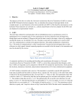
12. Connect the board to two USB ports of the host computer. One connection is to the port J16 of the
board (the one that is a Standard-B plug). The second connection is via the ULINK2
debugger/programmer/emulator. These connections are illustrated in Fig.1.
13. Download the program to the Flash of the microcontroller. Select Flash->Download. This loads the
blinky1.axf file. Then press the RESET push-button of the board.
14. Congratulations! You just programmed your first project. You should notice that the LED P1.29 is
blinking. If this is not the case, then you should investigate/debug your project to make it work.
Figure 1 Connection of ULINK2 to the board.
Debugging
If your program has errors (discovered by compiler or linker) or you simply want to debug it to verify its
operation, then we can use the debugging capabilities of the uVision tools.
1. Click Debug menu option and select Start/Stop Debug Session. A warning about the fact that this is an
evaluation version shows up; click OK.
2. Then, a new window appears where we can see the simulation of the program.
3. This window has several different supportive panels/sub-windows where we can monitor changes
during the simulation. The left hand side panel, Registers, provides information regarding the Registers
of LPC17xx with which we are working.
4. Again, click on the Debug menu option and select Run. The code starts simulating.
5. It is good practice that before going ahead with the actual hardware implementation to perform a
debug/simulation session to make sure that our program behaves according to the design requirements.
6. In our example, we use PORT1.
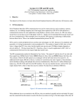
4
7. Go to Peripherals menu option then select GPIO Fast Interface followed by Port 1.
8. You should get the window shown in Fig.2 below, where you can see LED P1.29 blinking. To actually
observe this you should wait until the simulated time (shown on the bottom-right side of the uVision
ISE window) is longer than 1 second. Note that in order to actually simulate 1 second of execution time
of the program, the simulator must run much longer. This is expected, as typically simulators require
much longer computational runtimes (wallclock time) in order to simulate relatively short execution
times of the program under investigation!
9. This is a standard method to check that your program works correctly.
10. The debugger is a very powerful tool. This is only a brief exposure to it; we’ll revisit it many times later
in this course. Once you are done with the simulation/debug of your program, you can stop it by
selecting Start/Stop the Debug Session from the Debug menu option. This stops the show and takes us
back to the main uVision window.
Figure 2 Pin P1.29 is checked on/off every other second or so.
Taking it further
At this time, you should revisit blinky1.c file. Read this file (it has lots of comments) and browse
related/included files in order to fully understand what is what and what it does. This is very important.
You should take time to read/browse on your own the user’s guide of the board, the user manual and
datasheet of LPC17xx microcontrollers as well as other files included in the downloadable archive of this
lab [2-5]. Do not attempt to print them as some have >800 pages.
Note that because it is very difficult to cover everything during the lectures and labs, you are expected to
proactively engage materials related to this course and take ownership of your learning experience! This
is a necessary (but not sufficient) attitude to do well in this course.
b. BLINKY 2
Start uVision and select Project->Open Project, then, browse to open the Blinky project example located at:
C:\Keil460\ARM\Boards\Keil\MCB1700\Blinky
As you noticed, the ARM Kiel software installation contains a folder called Boards that contains design
examples for a variety of boards. We’ll use some of these design examples for the board utilized in this
course. However, as we go, you should take a look and play with all these examples; try to understand their
code.
Build the project and download to target. Observe operation and comment.
5
At this time, you should take time to read the .c files of this project, starting with Blinky.c. Read it and also
browse the other files to gain insights into what and how the code achieves different tasks. At this stage, do
not expect to understand everything; however, please make an effort to see as much as you can.
c. BLINKY 3
In this part of the lab, we implement the blinky example by writing a program in assembly language. In this
example we’ll turn on/off the LED controlled by pin P1.28. Start uVision and create a new project. Add to
it the following files:
1. When creating the project say Yes to have added startup_LPCxx.s to the project
2. blinky3.s (available in the downloadable archive of this lab as well in an ppendix at the end of this lab)
3. C:\Keil\ARM\Startup\NXP\LPC17xx\system_LPC17xx.c. This is needed for the SystemInit()
function called from within startup_LPCxx.s. We could not add this file to the project provided that
we comment out the two lines inside startup_LPCxx.s that contain SystemInit.
Build the project and download to target. Observe operation and comment.
At this time, you should take time to read the blinky3.s. Read it and make sure you understand how the
code achieves each task.
4. Lab Assignment
Modify the assembly program blinky3.s to implement the following design description: blink all eight
LEDs on the board, one by one from left to right repeatedly.
For each lab with a “Lab Assignment”, you must turn-in a lab report in PDF format (font size 11, single
spacing), named lab#_firstname_lastname.pdf (where “#” is the number of the lab, for example in the
case of lab1, “#” must be replaced with 1) which should contain the following sections:
Lab title, Your name
Introduction section – a brief description of the problem you solve in this lab assignment, outlining the
goal and design requirements.
Solution section – describe the main technique(s) that you utilized to develop your solution. Include
block diagrams, flow graphs, plots, etc. here to aid your explanation.
Results and Conclusion section – describe your results and any issues you may have faced during the
assignment and how you solved them.
Code listings, assembly or C code that you wrote. Appended at the end of your report. Use smaller font
(size 9) to save space.
For full credit, you must demo the correct operation of your assignment to the TA during the next lab.
While you are free to hand-write your report (still turned-in as a PDF file), please make sure your report is
neat and the presentation is coherent. You will lose points for reports that do not present enough details, are
ugly, disorganized, or are hard to follow/read.
5. Credits and references
[1] Software: Microcontroller Development Kit; download from http://www.keil.com/arm/mdk.asp
6
[2] Hardware: MCB1700 board User’s Guide;
http://www.keil.com/support/man/docs/mcb1700/mcb1700_su_connecting.htm
[3] LPC17xx user’s manual; http://www.nxp.com/documents/user_manual/UM10360.pdf
[4] NXP LPC17xx datasheet;
http://www.nxp.com/documents/data_sheet/LPC1769_68_67_66_65_64_63.pdf
http://www.keil.com/dd/chip/4868.htm
[5] Cortex-M3 information;
http://www.nxp.com/products/microcontrollers/cortex_m3/
http://www.arm.com/products/processors/cortex-m/cortex-m3.php
[6] Additional resources
--Keil uVision User’s Guide
http://www.keil.com/support/man/docs/uv4/
-- Keil uVision4 IDE Getting Started Guide
www.keil.com/product/brochures/uv4.pdf
--ARM Assembler Guide
http://www.keil.com/support/man/docs/armasm/
--ARM Compiler toolchain for uVision. Particularly browse:
ARM Compiler toolchain for uVision, Using the Assembler
ARM Compiler toolchain for µVision, Using the Linker
http://infocenter.arm.com/help/index.jsp?topic=/com.arm.doc.dui0377c/index.html
--Professor J.W. Valvano (UTexas) resources;
http://users.ece.utexas.edu/~valvano/Volume1/uvision/
--UWaterloo ECE254, Keil MCB1700 Hardware Programming Notes
https://ece.uwaterloo.ca/~yqhuang/labs/ece254/doc/MCB1700_Hardware.pdf
----EE 472 Course Note Pack, Univ. of Washington, 2009,
http://abstract.cs.washington.edu/~shwetak/classes/ee472/notes/472_note_pack.pdf (Chapter 6)
APPENDIX A: Some info on LPC1768 peripherals programming
Pins on LPC1768 are divided into 5 ports indexed from 0 to 4. Pin naming convention is Px.y, where x is
the port number and y is the pin number. For example, P1.29 means Port 1, Pin 29. Each pin has four
operating modes: GPIO (default), first alternate function, second alternate function, and third alternate
function. Any pin of ports 0 and 2 can be used to generate an interrupt.
To use any of the LPC1768 peripherals, the general steps to be followed are:
1. Power Up the peripheral to be used
2. Set the Clock Rate for the peripheral
3. Specify the pin operating mode - Connect necessary pins using Pin Connect Block
4. Set direction - Initialize the registers of the peripheral
1. Power Up the peripheral
Let’s assume we are interested in utilizing the pin P1.29 to drive one of the board’s LEDs on and off
(the blinky1 example). Refer to LPC17xx User’s Manual, Chapter 4: Clocking and Power Control.
Look for register Power Control for Peripherals register, PCONP. It’s on page 63; bit 15 is PGPIO.
Setting this bit to 1 should power up the GPIO ports. Note that the default value is 1 anyway, which
7
means GPIO ports are powered up by default on reset; but the start up code may modify this. Hence,
it’s good practice to make sure we take care of it. For example, here is how we power up the GPIO:
LPC_SC->PCONP |= 1 << 15;
2. Set desired clock to the peripheral
In the same Chapter 4 of the manual, look for Peripheral Clock Selection register, PCLKSEL1; it's on
page 57; bits 3:2 set the clock divider for GPIO. In our example, since we're not using interrupts, we
won’t change the default value. Note that PCLK refers to Peripheral Clock and CCLK refers to CPU
Clock. PCLK is obtained by dividing CCLK; see table 42 on page 57 of the manual;
3. Specify the pin operating mode - Connect necessary pins using Pin Connect Block
To specify the pin operating mode we configure PINSEL registers in the Pin Connect
Block(LPC_PINCON macro defined in LPC17xx.h). There are eleven PINSEL registers: PINSEL0,
PINSEL1, …, PINSEL10, which are defined as member variables inside the LPC_PINCON_TypeDef
C struct. Each one of these eleven registers controls a specific set of pins on a certain port. When the
processor powers up or resets, the pins that are connected to the LEDs and joystick are automatically
configured as GPIO (default). Hence, in our example, there is no need to change settings in the pin
connect block. However, it is a good practice to configure these pins before using them.
Refer to Section 8.1 of LPC17xx user’s manual to see which set of pins are controlled by which
PINSEL register. As an example, the five button joystick is connected to pins P1.20, P1.23, P1.24,
P1.25 and P1.26. As mentioned earlier, it is a good programming practice to configure it. Refer to page
109, Section 8.5.4, Table 82 in LPC17xx User’s Manual for more detailed information.
LPC_PINCON->PINSEL3 &= ~((3<< 8)|(3<<14)|(3<<16)|(3<<18)|(3<<20));
// P1.20, P1.23, …, P1.26 are GPIO (Joystick)
4. Set direction - Initialize the registers of the peripheral
In this step of programming of a GPIO pin, we set the I/O direction (i.e., pin to be used as input or
output). This is done via FIODIR register (see Chapter 9, page 122 of LPC17xx User’s Manual for
more info). There are five LPC_GPIOx, where x=0,1,2,3,4, macros defined in LPC17xx.h. The FIODIR
is a member variable in LPC_GPIO_TypeDef C struct in LPC17xx.h. To set a pin as input, set the
corresponding bit in FIODIR to 0. All I/Os default to input (i.e., all bits in FIODIR are default to logic
0). To set a pin as output, set the corresponding bit in FIODIR to 1. For example, to set pins connected
to the joystick as input, we write the following C code:
LPC_GPIO1->FIODIR &= ~((1<<20)|(1<<23)|(1<<24)|(1<<25)|(1<<26));
// P1.20, P1.23, ..., P1.26 are input (Joystick)
In our blinky example, we set all pins connected to the 8 LEDs as output. We achieve that via the
following C code:
LPC_GPIO1->FIODIR |= 0xB0000000; // pins P1.28, P1.29, P1.31 as output
LPC_GPIO2->FIODIR |= 0x0000007C; // pins P2.2, 3, 4, 5, 6 as output
Once a pin is set as output or input it can be utilized in our programs to drive or read logic values.
a) The pin is set as output
8
We turn a pin to HIGH/LOW (i.e., digital logic 1/0) by setting the corresponding bit in
FIOSET/FIOCLR register. Both FIOSET and FIOCLR are member variables defined in the
PC_GPIO_TypeDef C struct. To set a pin to digital 1, set the corresponding bit of LPC_GPIOx>FIOSET to 1. To turn a pin to digital 0, set the corresponding bit of LPC_GPIOx->FIOCLR to 1.
Refer to Sections 9.5.2 and 9.5.3 of LPC17xx User’s manual for details.
For example, to turn on LED P1.29, the following code can be used:
LPC_GPIO1->FIOSET = 1 << 29;
In general, to turn any of the 8 LEDs on, one can use the following trick:
const U8 led_pos[8] = { 28, 29, 31, 2, 3, 4, 5, 6 };
mask = 1 << led_pos[led];
if (led < 3) { // P1.28,29,31 are part of Port1
LPC_GPIO1->FIOSET = mask;
} else { // P2.2,3,4,5,6 are part of Port2
LPC_GPIO2->FIOSET = mask;
}
Of course, to turn off a particular LED, just replace FIOSET with FIOCLR in the above code.
Note: we can also set HIGH/LOW a particular output pin via the FIOPIN register. We can write
specific bits of the FIOPIN register to set the corresponding pin to the desired logic value. In this
way, we bypass the need to use both the FIOSET and FIOCLR registers. However, this is not the
recommended method. For example, in the case of the blinky example, we use the following C code:
LPC_GPIO1->FIOPIN |= 1 << 29; // make P1.29 high
LPC_GPIO1->FIOPIN &= ~( 1 << 29 ); // make P1.29 low
b) The pin is set as input
We read the current pin state from FIOPIN register. The corresponding bit being 1 indicates that the
pin is driven high. The corresponding bit being 0 indicates that the pin is driven low. The FIOPIN is
a member variable defined in LPC_GPIO_TypeDef C struct. One normally uses bit shift operations
to shift the LPC_GPIOx->FIOPIN value to obtain pin value(s). Refer to Section 9.5.4 in the
LPC17xx User’s manual for details. For example, to read the joystick position, the following code
can be used
#define KBD_MASK 0x79
uint32_t kbd_val;
kbd_val = (LPC_GPIO1->FIOPIN >> 20) & KBD_MASK;
When the joystick buttons are inactive, the bits located at P1.23,24,25,26 are logic 1. When any of
the joystick buttons becomes active, the bit corresponding to that pin becomes 0.
APPENDIX B: Listing of blinky3.s
; CopyLeft (:-) Cristinel Ababei, SUNY at Buffalo, 2012
; this is one assembly implementation of the infamous blinky example;
9
; target microcontroler: LPC1768 available on board Keil MCB1700 (or Embest EM-LPC1700 board)
; I tested it first on EM-LPC1700 board as it's cheaper!
;
; Note1: it has lots of comments, as it is intended for the one who
; sees for the first time assembly;
; Note2: some parts of the implementation are written in a more complicated manner
; than necessary for the purpose of illustrating for example different memory
; addressing methods;
; Note3: each project will have to have added to it also system_LPC17xx.s (added
; automatically by Keil uVision when you create your project) and system_LPC17xx.c
; which you can copy from your install directory of Keil IDE (for example,
; C:\Keil\ARM\Startup\NXP\LPC17xx\system_LPC17xx.c)
; Note4: system_LPC17xx.s basically should contain the following elements:
; -- defines the size of the stack
; -- defines the size of the heap
; -- defines the reset vector and all interrupt vectors
; -- the reset handler that jumps to your code
; -- default interrupt service routines that do nothing
; -- defines some functions for enabling and disabling interrupts
; Directives
; they assist and control the assembly process; directives or "pseudo-ops"
; are not part of the instruction set; they change the way the code is assembled;
; THUMB directive placed at the top of the file to specify that
; code is generated with Thumb instructions;
THUMB
; some directives define where and how the objects (code and variables) are
; placed in memory; here is a list with some examples:
; AREA, in assembly code, the smallest locatable unit is an AREA
; CODE is the place for machine instructions (typically flash ROM)
; DATA is the place for global variables (typically RAM)
; STACK is the place for the stack (also in RAM)
; ALIGN=n modifier starts the area aligned to 2^n bytes
; |.text| is used to connect this program with the C code generated by
; the compiler, which we need if linking assembly code to C code;
; it is also needed for code sections associated with the C library;
; NONINT defines a RAM area that is not initialized (normally RAM areas are
; initialized to zero); Note: ROM begins at 0x00000000 and RAM begins at
; 0x2000000;
; EXPORT is a directive in a file where we define an object and
; IMPORT directive is used in a file from where we wish to access the object;
; Note: we can export a function in an assembly file and call the function
; from a C file; also, we can define a function in C file, and IMPORT the function
; into an assembly file;
; GLOBAL is a synonym for EXPORT
; ALIGN directive is used to ensure the next object is aligned properly; for example,
; machine instructions must be half-word aligned, 32-bit data accessed with LDR, STR
; must be word-aligned; good programmers place an ALIGN at the end of each file so the
; start of every file is automatically aligned;
; END directive is placed at the end of each file
; EQU directive gives a symbolic name to a numeric constant, a register-relative
; value or a program-relative value; we'll use EQU to define I/O port addresses;
AREA |.text|, CODE, READONLY ; following lines are to be placed in code space
EXPORT
__main
ENTRY
10
; EQUates to make the code more readable; to turn LED P1.28 on and off
; we will write the bit 28 of the registers FIO1SET (to set HIGH) and FIO1CLR (to set LOW);
; refer to page 122 of the LPC17xx user manual to see the adresses of these registers; they are:
FIO1SET
EQU 0x2009C038
FIO1CLR
EQU 0x2009C03C
; we will implement a dirty delay by decrementing a large enough
; number of times a register;
LEDDELAY EQU 10000000
__main
; (1) we want to set as output the direction of the pins that
; drive the 8 LEDs; these pins belong to the ports Port 1 and Port 2
; and are: P1.28, P1,29, P1.31 and P2.2,...,6
; to set them as output, we must set to 1 the corresponding bits in
; registers (page 122 of LPC17xx user manual):
; FIO1DIR - 0x2009C020
; FIO2DIR - 0x2009C040
; that is, we'll set to 1 bits 28,29,31 of the register at adress 0x2009C020,
; which means writing 0xB0000000 to this location; also, we'll set 1 bits 2,...,6
; of the register at address 0x2009C040, which means writing 0x0000007C to
; this location;
MOV R1, #0x0 ; init R1 register to 0 to "build" address
MOVT R1, #0x2009 ; assign 0x20090000 to R1; MOVT assigns to upper nibble
MOV R3, #0xC000 ; move 0xC000 into R3
ADD R1, R1, R3 ; add 0xC000 to R1 to get 0x2009C000
MOV R4, #0xB0000000 ; place 0xB0000000 (i.e., bits 28,29,31) into R4
; now, place contents of R4 (i.e. 0xB0000000) to address
; 0x2009C020 (i.e., register FIO1DIR); this sets pins
; 28,29,31 as output direction;
; Note: address is created by adding the offset 0x20 to R1
; Note: the entire complication above could be replaced with
; simply loading R1 with =FIO1DIR (but we wanted to experiment with
; different flavors of MOV, to upper and lower nibbles); we'll use
; the simpler version later;
STR R4, [R1, #0x20]
MOV R4, #0x0000007C ; value to go to register of Port 2
STR R4, [R1, #0x40] ; set output direction for pins of Port 2 by writing to reister FIO2DIR
; (2) set HIGH the LED driven by P1.28; to do that we load current
; contents of register FIO1SET (i.e., memory address 0x2009C038) to R3,
; set to 1 its 28th bit, and then put it back into the location at
; memory address 0x2009C038 (i.e., effectively writing into register FIO1SET);
LDR R1, =FIO1SET ; we'll not touch R1 anymore so that it keeps this address
LDR R3, [R1]
ORR R3, #0x10000000 ; set to logic 1 bit 28 of R3
STR R3, [R1]
; (3) some initializations
LDR R0, =LEDDELAY ; initialize R0 for countdown
LDR R2, =FIO1CLR ; we'll not touch R2 anymore so that it keeps this address
; now, the main thing: turn the LED P1.28 on and off repeatedly;
; this is done by setting the bit 28 of registers FIO1CLR and FIO1SET;
; Note: one could do this in a simpler way by using a toggling trick:
; toggle (could be done using exclusive or with 1) bit 28 of register
; FIO1PIN instead (page 122 of LPC17xx user manual) and not use
; FIO1CLR and FIO1SET; I do not recommend however this trick as
11
; due to the peculiarities of FIO1PIN;
loop
led_on
SUBS R0, #1 ; decrement R0; this sets N,Z,V,C status bits
BNE led_on ; if zero not reached yet, go back and keep decrementing
LDR R3, [R2] ; recall that R2 stores =FIO1CLR
ORR R3, #0x10000000 ; set to logic 1 bit 28 of R3
STR R3, [R2] ; place R3 contents into FIO1CLR, which will put pin on LOW
LDR R0, =LEDDELAY ; initialize R0 for countdown
led_off
SUBS R0, #1 ; decrement R0; this sets N,Z,V,C status bits
BNE led_off ; if zero not reached yet, go back and keep decrementing
LDR R3, [R1] ; recall that R1 stores =FIO1SET
ORR R3, #0x10000000 ; set to logic 1 bit 28 of R3
STR R3, [R1] ; place R3 contents into FIO1SET, which will put pin on HIGH
LDR R0, =LEDDELAY ; initialize R0 for countdown
; now do it again;
B loop
ALIGN
END
12
Lab 2: Using UART
1. Objective
The objective of this lab is to utilize the Universal Asynchronous Receiver/Transmitter (UART) to connect
the MCB1700 board to the host computer. Also, we introduce the concept of interrupts briefly. In the
example project, we send characters to the microcontroller unit (MCU) of the board by pressing keys on the
keyboard. These characters are sent back (i.e., echoed, looped-back) to the host computer by the MCU and
are displayed in a hyperterminal window.
2. UART
The most basic method for communication with an embedded processor is asynchronous serial. It is
implemented over a symmetric pair of wires connecting two devices (referred as host and target here,
though these terms are arbitrary). Whenever the host has data to send to the target, it does so by sending an
encoded bit stream over its transmit (TX) wire. This data is received by the target over its receive (RX)
wire. The communication is similar in the opposite direction. This simple arrangement is illustrated in
Fig.1. This mode of communications is called “asynchronous” because the host and target share no time
reference (no clock signal). Instead, temporal properties are encoded in the bit stream by the transmitter and
must be decoded by the receiver.
Figure 1 Basic serial communication.
A commonly used device for encoding and decoding such asynchronous bit streams is a Universal
Asynchronous Receiver/Transmitter (UART). UART is a circuit that sends parallel data through a serial
line. UARTs are frequently used in conjunction with the RS-232 standard (or specification), which specifies
the electrical, mechanical, functional, and procedural characteristics of two data communication equipment.
A UART includes a transmitter and a receiver. The transmitter is essentially a special shift register that
loads data in parallel and then shifts it out bit by bit at a specific rate. The receiver, on the other hand, shifts
in data bit by bit and reassembles the data. The serial line is ‘1’ when it is idle. The transmission starts with
a start-bit, which is ‘0’, followed by data-bits and an optional parity-bit, and ends with stop-bits, which are
‘1’. The number of data-bits can be 6, 7, or 8. The optional parity bit is used for error detection. For odd
parity, it is set to ‘0’ when the data bits have an odd number of ‘1’s. For even parity, it is set to ‘0’ when the
data-bits have an even number of ‘1’s. The number of stop-bits can be 1, 1.5, or 2. The transmission with 8
data-bits, no parity, and 1 stop-bit is shown in Fig.2 (note that the LSB of the data word is transmitted first).
Figure 2 Transmission of a byte.
13
No clock information is conveyed through the serial line. Before the transmission starts, the transmitter and
receiver must agree on a set of parameters in advance, which include the baud-rate (i.e., number of bits per
second), the number of data bits and stop bits, and use of parity bit.
To understand how the UART's receiver extracts encoded data, assume it has a clock running at a multiple
of the baud rate (e.g., 16x). Starting in the idle state (as shown in Fig.3), the receiver “samples” its RX
signal until it detects a high-low transition. Then, it waits 1.5 bit periods (24 clock periods) to sample its RX
signal at what it estimates to be the center of data bit 0. The receiver then samples RX at bit-period intervals
(16 clock periods) until it has read the remaining 7 data bits and the stop bit. From that point this process is
repeated. Successful extraction of the data from a frame requires that, over 10.5 bit periods, the drift of the
receiver clock relative to the transmitter clock be less than 0.5 periods in order to correctly detect the stop
bit.
Figure 3 Illustration of signal decoding.
UARTs can be used to interface to a wide variety of other peripherals. For example, widely available
GSM/GPRS cell phone modems and Bluetooth modems can be interfaced to a microcontroller UART.
Similarly GPS receivers frequently support UART interfaces.
The NXP LPC1768 microcontroller includes four such devices/peripherals called UARTs: UART0/2/3 and
UART1. See pages 298 and 318 of the LPC17xx User’s Manual [1]. See also page 27 of the Datasheet [2].
UART0 and UART1 of the microcontroller are connected on the MCB1700 board to the ST3232C (IC6),
which converts the logic signals to RS-232 voltage levels. This connection is realized from pins
{P0.2/TXD0/AD0.7 and P0.3/RXD0/AD0.6} and { P2.0/PWM1.1/TXD1 and P2.1/PWM1.2/RXD1} of the
microcontroller to the pins {10, 9, 11, and 12} ST3232C chip. The ST3232C chip drives the two COM0
and COM1 represented by the two female DB9 connectors (Note: if you use an Embest LPC1700 board,
then, note that these two connectors are male DB9 connectors). To see these connections, take a look on
pages 1 and 3 of the schematic diagram of the board [3] (included also in the downloadable files of this
lab#2).
For more details on UART and RS-232, please read references [1-6].
In this lab we will explore serial communication between the (target) LPC1768 UART and a serial
communication port of the host PC.
3. EXAMPLE 1: Microcontroller “echoes” back the characters sent by host computer
(a) Experiment
In the first example of this lab, we’ll use an example project that comes with the “LPC1700 code bundle”.
The LPC1700 Code Bundle is a free software package from NXP that demonstrates the use of the built-in
peripherals on the NXP LPC17xx series of microcontrollers. The example software includes a common
library, peripheral APIs, and test modules for the APIs.
14
Download LPC1700 Code Bundle from [7] (http://ics.nxp.com/support/software/code.bundle.lpc17xx.keil/)
and save it in your own work directory. Save it with the plan to keep it as we’ll revisit some other example
in the future. Unzip it to get the keil_examples folder created with several examples therein. Take a minute
and read keil_example/readme.txt now.
Launch Keil uVision4 and then open the project UART from among the example just downloaded. The
UART project is a simple program for the NXP LPC17xx microcontrollers using Keil’s MCB1700
evaluation board. When sending some characters from a terminal program on the PC at a speed of 57600
Baud to the LPC17xx UART0 or UART1 the LPC17xx will echo those same characters back to the
terminal program.
Step 1: Connect the board, ULINK2, and the host computer as shown in Fig.4. Ask the TA for the COM0/1
to Serial Port cable.
Figure 4 Hardware setup.
Remove the RST and ISP jumpers. Please keep the jumpers safe and place them back when you are done
with this lab.
Note: If you are doing this lab using a laptop which does not have a serial port, you can use a USB Serial
Converter. I got mine for about $12 from Amazon [8] and it works great.
Step 2: Familiarize yourself with the following files:
--uart.c: contains the UART0 / UART1 handlers / driver functions
--uarttest.c: contains a small test program utilizing the UART driver
--system_LPC17xx.c: Cortex-M3 Device Peripheral Access Layer Source File
--startup_LPC17xx.s: CMSIS Cortex-M3 Core Device Startup File
--Abstract.txt: Describes what the uarttest.c program does
Change "#include "lpc17xx.h" to "#include <lpc17xx.h>. This is done in order to use the latest Keil’s
release of the header file (normally located in C:\Keil\ARM\INC\NXP directory).
Step 3: Make sure the uVision4 Target setting is FLASH. Then, build the project by rebuilding all target
files. Download to the microcontroller and confirm that download is ok.
Step 4: Establish a Terminal connection
--Method 1: If your Windows is XP or older, you can use HyperTerminal:
15
--Start HyperTerminal by clicking Start - > All Programs -> Accessories -> Communications ->
HyperTerminal
--Connect HyperTerminal to the serial port that is connected to the COM0 port of the evaluation board for
example. For the HyperTerminal settings you should use: COM1 (double check that it the host’s serial port
is indeed COM1in your case – you can do that by Start->Control Panel->System->Hardware->Device
Manager and click on Ports (COM & LPT); if in your case it’s a different port number then use that; for
example, in my case as I use the USB to serial adapter with my laptop, the port is COM14), baud rate
57600, 8 data bits, no parity, 1 stop bit, and no flow control.
--Method 2: If your Windows is 7 or newer, you first must make sure you download and/or install a serial
connection interface (because HyperTerminal is not part of Windows 7 or later). On the machines in the
lab, you can use Putty (http://www.putty.org):
--Start->All Programs->Putty->Putty
--Then, select Connection, Serial and type COM1 (or whatever is in your case; find what it is as described
in Method 1), baud rate 57600, 8 data bits, no parity, 1 stop bit, and no flow control.
--Click on Session and choose the type of connection as Serial. Save the session for example as "lab2".
--Finally, click on Open; you should get HyperTerminal like window.
--Method 3: You can use other programs such as:
TeraTerm (http://logmett.com/index.php?/products/teraterm.html) or
HyperSerialPort (http://www.hyperserialport.com/index.html) or
RealTerm (http://realterm.sourceforge.net) or CoolTerm (http://freeware.the-meiers.org), etc.
Step 5: Type some text. It should appear in the HyperTerminal window. This is the result of: First, what
you type is sent to the microcontroller via the serial port (that uses a UART). Second, the MCU receives
that via its own UART and echoes (sends back) the typed characters using the same UART. The host PC
receives the echoed characters that are displayed in the HyperTerminal.
Disconnect the serial cable from COM0 and connect it to COM1 port on the MCB1700 board. The behavior
of project should be the same.
Step 6: (optional – do not do it on computers in the lab): On your own computer only, download and install
NXP’s FlashMagic tool from here:
http://www.flashmagictool.com/
Then, follow the steps that describe how to use this tool as presented in the last part of the UART
documentation for the code bundle:
http://ics.nxp.com/literature/presentations/microcontrollers/pdf/code.bundle.lpc17xx.keil.uart.pdf (included
in the downloadable archive of files for this lab).
Note: With this approach one does not need the ULINK2 programmer/debugger.
(b) Brief program description
Looking at the main() function inside the uarttest.c file we can see the following main actions:
--UART0 and UART1 are initialized:
UARTInit(0, 57600);
UARTInit(1, 57600);
/* baud rate setting */
/* baud rate setting */
--A while loop which executes indefinitely either for UART0 or for UART1. The instructions executed
inside this loop (let’s assume the UART0) are:
16
Disable Receiver Buffer Register (RBR), which contains the next received character to be read. This is
achieved by setting all bits of the Interrupt Enable Register (IER) to ‘0’ except bits THRE and RLS. In
this way the LSB (i.e., bit index 0 out of 32 bits) of IER register is set to ‘0’. The role of this bit (as
explained in the LPC17xx User’s Manual [1] on page 302) when set to ‘0’ is to disable the Receive
Data Available interrupt for UART0.
Send back to the host the characters from the buffer UART0Buffer. This is done only if there are
characters in the buffer (the total buffer size is 40 characters) which have been received so far from the
host PC. The number of characters received so far and not yet echoed back is stored and updated in
UART0Count.
Once the transmission of all characters from the buffer is done, reset the counter UART0Count.
Enable Receiver Buffer Register (RBR). This is achieved by setting to ‘1’ the LSB of IER, which in
turn is achieved using the mask IER_RBR.
(c) Source code discussion
Please take your time now to thoroughly browse the source code in files uart.c and uarttest.c files. Open
and read other files as necessary to track the declarations and descriptions of variables and functions.
For example, in uarttest.c we see:
--A function call SystemClockUpdate();
This is described in source file system_LPC17xx.c which we locate in the Project panel of the uVision4
IDE. Click on the name of this file to open and search inside it the description of SystemClockUpdate().
This function is declared in header file system_LPC17xx.h. Open these files and try to understand how this
function is implemented; what each of the source code lines do?
--A function call UARTInit(0, 57600);
This function is described in source file uart.c. The declaration of this function is done inside header file
uart.h. Open these files and read the whole code; try to understand each line of the code.
--An instruction:
LPC_UART0->IER = IER_THRE | IER_RLS;
/* Disable RBR */
Based on what’s been studied in lab#1 you should know already that LPC_UART0 is an address of a
memory location – the UART0 peripheral is “mapped” to this memory location. Starting with this memory
location, several consecutive memory locations represent “registers” associated with this peripheral/device
called UART0. All 14 such registers (or memory locations) are listed on page 300 of the User Manual.
Utilizing this peripheral is done through reading/writing into these registers according to their meaning and
rules described in the manual. For example, one of the 14 registers associated with UART0 is Interrupt
Enable Register (IER).
Form a C programming perspective, LPC_UART0 is declared inside header file LPC17xx.h:
#define LPC_UART0
((LPC_UART_TypeDef
*) LPC_UART0_BASE
)
Which also declares what LPC_UART0_BASE as:
#define LPC_UART0_BASE
(LPC_APB0_BASE + 0x0C000)
Where LPC_APB0_BASE is declared at its turn in the same file:
#define LPC_APB0_BASE
(0x40000000UL)
This effectively makes LPC_UART0_BASE to have value: 0x4000C000, which not surprisingly coincides
with what is reported on page 14 of the LPC17xx User’s Manual!
Furthermore, the Interrupt Enable Register (IER) contains individual interrupt enable bits for the 7 potential
UART interrupts. The IER register for UART0 is “mapped” (or associated with) to memory address
17
0x4000C004 as seen on page 300 of the LPC17xx User’s Manual. This fact is captured in the struct
declaration of LPC_UART_TypeDef inside the header file LPC17xx.h (open this file and double check
it!). As a result, in our C programming, we can refer to the IER register as in the instruction that we are
currently discussing: LPC_UART0->IER, which basically stores/represents the address 0x4000C004.
In addition, note that IER_THRE and IER_RLS are declared inside the header file uart.h as:
#define IER_THRE
#define IER_RLS
0x02
0x04
Which are utilized as masks in our instruction:
LPC_UART0->IER = IER_THRE | IER_RLS;
/* Disable RBR */
So, finally as we see, the effect of this instruction is simply to turn ‘1’ bit index 1 (the second LSB out of 32
bits) and bit index 2 (the third LSB out of 32 bits) of the IER register! All other bits are set to ‘0’.
Having bit index 1 of this register set to ‘1’ enables the Transmit Holding Register Empty (THRE) flag for
UART0 – see page 302, Table 275 of the LPC17xx User’s Manual. Having bit index 2 of this register set to
‘1’ enables the UART0 RX line status interrupts – see page 302, Table 275 of the LPC17xx User’s Manual.
As already said, all other bits are set therefore via this masking to ‘0’. This includes the LSB (i.e., bit index
0 out of 32 bits) of IER register, which is set to ‘0’. The role of this bit (as explained in the LPC17xx User’s
Manual on page 302) when set to ‘0’ is to disable the Receive Data Available interrupt for UART0.
You should be able now to explain what the following instruction does:
LPC_UART0->IER = IER_THRE | IER_RLS | IER_RBR;
/* Re-enable RBR */
Summarizing, what the code inside uarttest.c does is (as also mentioned in the previous section):
--disable receiving data
--send back data to the PC from the buffer (i.e., array variable UART0Buffer)
--reset counter of characters stored in buffer
--enable receiving data
Note: As mentioned in lab#1, in general one would not need to worry about these details about addresses to
which registers are mapped. It would be sufficient to just know of for example the definition and declaration
of LPC_UART_TypeDef inside the header file LPC17xx.h. To the C programmer, it is transparent to what
exact address the register IER is mapped to for example. However, now at the beginning, it’s instructive to
track these things so that we get a better global picture of these concepts. It also forces us to get better used
with the LPC17xx User’s Manual and the datasheets.
Notice that inside the source file uart.c we have these two function descriptions:
void UART0_IRQHandler (void) {...}
void UART1_IRQHandler (void) {...}
which are not called for example inside uarttest.c, but they appear inside startup_LPC17xx.s:
DCD
UART0_IRQHandler
; 21: UART0
DCD
UART1_IRQHandler
; 22: UART1
The function void UART0_IRQHandler (void) is the UART0 interrupt handler. Its name is
UART0_IRQHandler because it is named like that by the startup code inside the file startup_LPC17xx.s.
DCD is an assembler directive (or pseudo-op) that defines a 32-bit constant.
To get a better idea about these things, we need to make a parenthesis and discuss a bit about interrupts in
the next section. For the time being this discussion is enough. We will discuss interrupts in more details in
class lectures and in some of the next labs as well.
18
---------------------------------------------------------------------------------------------------------------------------------(d) Interrupts – a 1st encounter
An interrupt is the automatic transfer of software execution in response to a hardware event that is
asynchronous with the current software execution. This hardware event is called a trigger. The hardware
event can either be a busy to ready transition in an external I/O device (i.e., peripheral, like for example the
UART input/output) or an internal event (like bus fault, memory fault, or a periodic timer). When the
hardware needs service, signified by a busy to ready state transition, it will request an interrupt by setting its
trigger flag.
A thread is defined as the path of action of software as it executes. The execution of the interrupt service
routine (ISR) is called as a background thread, which is created by the hardware interrupt request and is
killed when the ISR returns from interrupt (e.g., by executing a BX LR in an assembly program). A new
thread is created for each interrupt request. In a multi-threaded system, threads are normally cooperating to
perform an overall task. Consequently, we’ll develop ways for threads to communicate (e.g., FIFOs) and
synchronize with each other.
A process is also defined as the action of software as it executes. Processes do not necessarily cooperate
towards a common shared goal. Threads share access to I/O devices, system resources, and global variables,
while processes have separate global variables and system resources. Processes do not share I/O devices.
To arm (disarm) a device/peripheral means to enable (shut off) the source of interrupts. Each potential
interrupting trigger has a separate “arm” bit. One arms (disarms) a trigger if one is (is not) interested in
interrupts from this source.
To enable (disable) means to allow interrupts at this time (postponing interrupts until a later time). On the
ARM Coretx-M3 processor, there is one interrupt enable bit for the entire interrupt system. In particular, to
disable interrupts we set the interrupt mask bit, I, in PRIMASK register.
Note: An interrupt is one of five mechanisms to synchronize a microcontroller with an I/O device. The
other mechanisms are blind cycle, busy wait, periodic polling, and direct memory access. With an input
device, the hardware will request an interrupt when input device has new data. The software interrupt
service will read from the input device and save in global RAM. With an output device, the hardware will
request an interrupt when the output device is idle. The software interrupt service will get data from a
global structure, and write it to the device. Sometimes, we configure the hardware timer to request
interrupts on a periodic basis. The software interrupt service will perform a special function; for example, a
data acquisition system needs to read the ADC at a regular rate.
On the ARM Cortex-M3 processor, exceptions include resets, software interrupts, and hardware
interrupts. Each exception has an associated 32-bit vector that points to the memory location where the
ISR that handles the exception is located. Vectors are stored in ROM at the beginning of the memory. Here
is an example of a few vectors as defined inside startup_LPC17xx.s:
__Vectors
DCD
DCD
DCD
DCD
...
__initial_sp
Reset_Handler
NMI_Handler
HardFault_Handler
;
;
;
;
19
Top of Stack
Reset Handler
NMI Handler
Hard Fault Handler
; External Interrupts
DCD
WDT_IRQHandler
DCD
TIMER0_IRQHandler
...
DCD
UART0_IRQHandler
...
; 16: Watchdog Timer
; 17: Timer0
; 21: UART0
ROM location 0x00000000 has the initial stack pointer and location 0x00000004 contains the initial
program counter (PC), which is called the reset vector. It points to a function called reset handler, which is
the first thing executed following reset.
Interrupts on the Cortex-M3 are controlled by the Nested Vector Interrupt Controller (NVIC). To activate
an “interrupt source” we need to set its priority and enable that source in the NVIC (i.e., activate =
set priority + enable source in NVIC). This activation is in addition to the “arm” and “enable” steps
discussed earlier.
Table 50 in the User Manual (page 73) lists the interrupt sources for each peripheral function. Table 51
(page 76 in User Manual) summarizes the registers in the NVIC as implemented in the LPC17xx
microcontroller. Read the entire Chapter 6 of the User Manual (pages 72-90) and identify the priority and
enable registers and their fields of the NVIC. Pay particular attention to (i.e., search/watch for) UART0 in
this Chapter. How would you set the priority and enable UART0 as a source of interrupts?
---------------------------------------------------------------------------------------------------------------------------------Coming back to our discussion of the function void UART0_IRQHandler (void) in uart.c, we see a first
instruction:
IIRValue = LPC_UART0->IIR;
What does it do? It simply reads the value of LPC_UART0->IIR and assigns it to a variable whose name
is IIRValue. LPC_UART0->IIR is the value of the register IIR (Interrupt IDentification Register identifies which interrupt(s) are pending), which is one of several (14 of them) registers associated with the
UART0 peripheral/device. You can see it as well as the other registers on page 300 of the User Manual.
Take a while and read them all. The fields of the interrupt register IIR are later described on page 303 in the
User Manual. Take another while and read them all on pages 303-304.
Next inside uart.c we see:
IIRValue >>= 1;
IIRValue &= 0x07;
/* skip pending bit in IIR */
/* check bit 1~3, interrupt identification */
Which shifts right with one bit IIRValue and then AND’s it with 0x07. This effectively “zooms-in” onto the
field formed by bits index 1-3 from the original LPC_UART0->IIR, bits which are now in the position bits
index 0-2 of IIRValue variable.
Going on, we find an “if” instruction with several branches:
if (
{...
}
else
{...
}
else
{...
}
else
IIRValue == IIR_RLS )
/* Receive Line Status */
if ( IIRValue == IIR_RDA )
/* Receive Data Available */
if ( IIRValue == IIR_CTI )
/* Character timeout indicator */
if ( IIRValue == IIR_THRE )
/* THRE, transmit holding register empty */
20
{...
}
See in Table 276 on page 303 in the User Manual what is the meaning of the three bits 1-3 from the original
IIR register:
011
010
110
001
1 - Receive Line Status (RLS).
2a - Receive Data Available (RDA).
2b - Character Time-out Indicator (CTI).
3 - THRE Interrupt
For each of these situations, something else is done inside the corresponding branch of the “if” instruction
above. In other words, we first identify the interrupt, and for each ID we do something else. If none of the
expected IDs is found, we do nothing. Please take your time now to explain what’s done in each of these
cases. Read pages 303-304 in the User Manual for this. This is very important in order to understand the
overall operation of the example of this lab.
4. Lab Assignment
1) (not graded and should not be discussed in the lab report) Use a Debug session to step through the
execution of this program. The scope is for you to better understand its operation. See lab#1 for how to
use/run a debug session. See also documentation of the code bundle from NXP [7].
2) Answer the question: Why did we need to remove the ISP and RST jumpers in Example 1?
3) Describe in less than a page (typed, font size 11, single line spacing) all instructions inside the function
void UART0_IRQHandler (void) for each of the branches of the main “if” instruction. Include this in your
lab report.
4) Modify Example 1 such that the characters typed on the host’s keyboard are also displayed on the LCD
display on the board. (Hint: re-use code from Blinky2 example of lab#1)
5. Credits and references
[1] LPC17xx user’s manual; http://www.nxp.com/documents/user_manual/UM10360.pdf (part of lab#1
files)
[2] NXP LPC17xx Datasheet;
http://www.nxp.com/documents/data_sheet/LPC1769_68_67_66_65_64_63.pdf (part of lab#1 files)
[3] Schematic Diagram of the MCB1700 board; http://www.keil.com/mcb1700/mcb1700-schematics.pdf
(part of lab#2 files)
[4] MCB1700 Serial Ports; http://www.keil.com/support/man/docs/mcb1700/mcb1700_to_serial.htm
[5] UART entry on Wikipedia (click also on the references therein for RS-232);
http://en.wikipedia.org/wiki/Universal_asynchronous_receiver/transmitter
[6]
--Jonathan W. Valvano, Embedded Systems: Introduction to Arm Cortex-M3 Microcontrollers, 2012.
(Chapters 8,9)
--Pong P. Chu, FPGA Prototyping by VHDL Examples: Xilinx Spartan-3 Version, Wiley 2008. (Chapter 7)
--Lab manual of course http://homes.soic.indiana.edu/geobrown/c335 (Chapter 5)
--EE 472 Course Note Pack, Univ. of Washington, 2009,
http://abstract.cs.washington.edu/~shwetak/classes/ee472/notes/472_note_pack.pdf (Chapter 8)
[7] LPC1700 Code Bundle;
Download: http://ics.nxp.com/support/software/code.bundle.lpc17xx.keil/
21
Documentation:
http://ics.nxp.com/literature/presentations/microcontrollers/pdf/code.bundle.lpc17xx.keil.uart.pdf
[8] Pluggable USB to RS-232 DB9 Serial Adapter;
Amazon: http://www.amazon.com/Plugable-Adapter-Prolific-PL2303HXChipset/dp/B00425S1H8/ref=sr_1_1?ie=UTF8&qid=1359988639&sr=81&keywords=plugable+usb+to+serial
Tigerdirect: http://www.tigerdirect.com/applications/SearchTools/itemdetails.asp?EdpNo=3753055&CatId=464
22
Lab 3: Debugging and More on Interrupts
1. Objective
The objective of this lab is to learn about the different features of the debugger of uVision. We’ll do this by
experimenting with several examples. We’ll also re-emphasize some aspects about interrupts (UART and
Timer) via these examples.
2. uVision Debuger
The μVision Debugger is completely integrated into the μVision IDE. It provides many features, including
the following [1]:
--Disassembly of the code on C/C++ source- or assembly-level with program execution in various stepping
modes and various view modes, like assembler, text, or mixed mode
--Multiple breakpoint options including access and complex breakpoints
--Review and modify memory, variable, and register values
--List the program call tree including stack variables
--Review the status of on-chip microcontroller peripherals
--Debugging commands or C-like scripting functions
--Code Coverage statistics for safety-critical application testing
--Various analyzing tools to view statistics, record values of variables and peripheral I/O signals, and to
display them on a time axis
--Instruction Trace capabilities to view the history of executed instructions
The μVision Debugger offers two operating modes:
1) Simulator Mode - configures the μVision Debugger as a software-only product that accurately
simulates target systems including instructions and most on-chip peripherals (serial port, external I/O,
timers, and interrupts; peripheral simulation capabilities vary depending on the device you have
selected.). In this mode, you can test your application code before any hardware is available. It gives
you serious benefits for rapid development of reliable embedded software.
2) Target Mode - connects the μVision Debugger to real hardware. Several target drivers are available
that interface to a:
-ULINK JTAG/OCDS Adapter that connects to on-chip debugging systems
-Monitor that may be integrated with user hardware or that is available on many evaluation boards
-Emulator that connects to the microcontroller pins of the target hardware
-In-System Debugger that is part of the user application program and provides basic test functions
-ULINKPro Adapter a high-speed debug and trace unit connecting to on-chip debugging systems via
JTAG/SWD/SWV, and offering Cortex-M3ETM Instruction Trace capabilities
Debug Menu
The Debug Menu of uVision IDE includes commands that start and stop a debug session, reset the CPU,
run and halt the program, and single-step in high-level and assembly code. In addition, commands are
available to manage breakpoints, view RTOS Kernel information, and invoke execution profiling. You can
modify the memory map and manage debugger functions and settings.
23
Debug Toolbar
Take a moment and read pages 67-68 of the uV IDE Getting Started Guide [1]. The discussion on these
pages present all the icons of the IDE related to the debugger.
Pre-lab preparation
Please take some time now and read fully Chapters 7,8,9 from the uV IDE Getting Started Guide [1].
3. Example 1 – Blinky 1 Revisited
The files necessary for this example are located in example1 folder as part of the downloadable archive for
this lab. As mentioned earlier, the μVision Debugger can be configured as a Simulator or as a Target
Debugger. In this example, we’ll use the Simulator. Go to the Debug tab of the Options for Target dialog to
switch between the two debug modes and to configure each mode. Configure to Use Simulator. Before
running the simulation, replace the following two lines inside blinky1.c:
delay( 1 << 24 );
with:
delay( 1 << 14 );
This is to make the blinking of P1.29 faster inside the simulator; otherwise, we’d need to wait too long to
actually see the corresponding bit turning 1 or 0.
Simulation Debug
Open the Blinky1 project that you created in lab#1 or create a new project; use files from example1 folder.
11. Click Debug menu option and select Start/Stop Debug Session. A warning about the fact that this is an
evaluation version shows up; click OK.
12. Then, a new window appears where we can see the simulation of the program.
13. This window has several different supportive panels/sub-windows where we can monitor changes
during the simulation. The left hand side panel, Registers, provides information regarding the Registers
of LPC17xx with which we are working.
14. Again, click on the Debug menu option and select Run. The code starts simulating.
15. It is good practice that before going ahead with the actual hardware implementation to perform a
debug/simulation session to make sure that our program behaves according to the design requirements.
16. In our example, we use PORT1.
17. Go to Peripherals menu option then select GPIO Fast Interface followed by Port 1.
18. You should get the window that shows P1.29 blinking.
19. Stop the simulation: Debug->Stop or hit the Stop icon from the Toolbar.
Breakpoints
1. Let’s set two breakpoints on lines:
LPC_GPIO1->FIOPIN |= 1 << 29; // make P1.29 high
LPC_GPIO1->FIOPIN &= ~( 1 << 29 ); // make P1.29 low
inside blinky1.c. To set a breakpoint, right-click on each of these lines, on the left margin of the panel that
displays this file and then select Insert/Remove Breakpoint.
2. Go to Peripherals menu option then select GPIO Fast Interface followed by Port 1 to show the GPIO1
Fast Interface.
24
3. Debug->Run. Notice that the simulation starts and runs till the first breakpoint where it stops. Notice
that P1.29 is 0. To continue the simulation click the icon “Step (F11)” once. What happens? P1.29 is
turned 1 and we stepped with the simulation to the next instruction inside our program.
4. Step (F11) again more times. Observe what happens each time. While stepping inside the delay()
function, observe the value of local variable “i” inside the panel labeled Call Stack + Locals on the
bottom right side of the uVision IDE. Notice how “i” is incremented. To get out from within the delay()
function click the icon “Step out (Ctrl-F11)”.
5. Once you get a hang of it, stop the simulation.
Logic Analyzer
The debugger includes a logic analyzer that will allow you to study the relative timing of various signals
and variable changes. It’s activated using the button in the debugger. Note that you can only use the logic
analyzer when you’re running in the simulator, not on the board.
The logic analyzer is mostly self-explanatory. Use the Setup button to add channels. You can use symbolic
names such as FIO1PIN to determine what registers or variables to watch, and you can specify a mask value
(which is ANDed with the contents of the register or variable) and a right shift value (which is applied after
the AND operation). You can view the result as a numeric value (“analog”) or as a bit value. At any point
you can stop the updating of the screen (and/or stop the simulation itself), and change the resolution to
zoom in or out. You can also scroll forward and backward in time using the scrollbar below the logic
analyzer window. There are also “prev” and “next” buttons to move quickly from one transition to another.
1. Open the Logic Analyzer by clicking the icon Analysis Windows->Logic Analyzer
2. Click Setup… in the new window of the logic analyzer. Then, click New (Insert) icon and type
FIO1PIN. Type in 0x20000000 as “And Mask”.
3. Go to Peripherals menu option then select GPIO Fast Interface followed by Port 1 to show the GPIO1
Fast Interface.
4. Run simulation and observe how the signal changes inside the Logic Analyzer window.
4. Example 2 – UART1 sends “Hello World! “ Once Only
The files necessary for this example are located in example2 folder as part of the downloadable archive for
this lab. This example is a modified (simplified) version of the example from lab#2. The simplified version
uses only UART1 to simply send to the PC the string of characters “Hello World! “.
Please take a moment and read the new files uart.h, uart.c, and uarttest.c. Observe the differences
compared to the original example from lab#2. Discuss with your team member the functionality of this new
example.
To work with this example, go to your own folder where you have saved keil_examples/ (this is the codebundle of lab#2) and copy the whole directory UART/ to UART_modified/. Then, replace the files uart.h,
uart.c, and uarttest.c from UART_modified/ with the ones provided in folder example2 of the
downloadable archive of this lab. We make this copy and work inside keil_examples/ to avoid copying files
from keil_examples/common/ (such as type.h).
Launch uVision and open the project from UART_modified/. Build the project and download to the board
as you did in lab#2. Use a Putty terminal (or a HyperTerminal if you use Windows XP) to see that indeed
“Hello World! “ is printed out.
25
Simulation Debug
1. Configure the debugger to Use Simulator.
2. Click Debug menu option and select Start/Stop Debug Session.
3. Select View->Serial Windows->UART #2. In this window we can see what is sent out from UART1.
4. Select View->Watch Windows->Watch1. Double click on <Enter expression> inside the newly
opened window and type UART1TxEmpty. This will monitor the variable UART1TxEmpty.
5. Run and Step through the program simulation. Observe and comment.
Target Debug
1. Configure the debugger to ULINK2/ME Cortex Debugger.
2. Modify the following line inside uart.c:
volatile uint32_t UART1Count = 1;
We do this so that UART1 will transmit only one character, which we want to observe during debugging.
3. Build and download.
4. Click Debug menu option and select Start/Stop Debug Session.
5. Run and step through the execution of the program. Observe and comment. Identify the moment when
the execution is in the state shown in the figure below. This is the moment when character ‘H’ (which is
48 in HEX) stored in register R3 is going to be stored to memory location 0x4001000 (stored in register
R4), which if you look on page 320 of the user manual, you will see that it is register LPC_UART1>THR!
Figure 1 Illustration of the moment when 'H' is placed into register 0x40010000
26
5. Example 3 – Blink LED using Timer 0 Interrupt
The file necessary for this example is located in example3 folder as part of the downloadable archive for
this lab. We discussed this example in class (see lecture notes #9).
First, create a new uVision project and use the provided source file, blink1_lec09.c. Build and download.
Observe operation and comment. Also, take some time and read the file to remember anything that it does.
Target Debug
1. Configure the debugger to ULINK2/ME Cortex Debugger.
2. Click Debug menu option and select Start/Stop Debug Session.
3. Open the Logic Analyzer by clicking the icon Analysis Windows->Logic Analyzer
4. Click Setup… in the new window of the logic analyzer. Then, click New (Insert) icon and type
FIO1PIN. Type in 0x20000000 as “And Mask”.
5. Go to Peripherals menu option then select GPIO Fast Interface followed by Port 1 to show the GPIO1
Fast Interface.
6. Run simulation and step through the execution of the program. Observe how the signal changes inside
the Logic Analyzer window as well as inside the peripheral monitoring window. Comment.
6. Example 4 – Drawing circles on the 320x240 pixels LCD display of the MCB1700 board
You are given two versions of this example: Version 1 files are located in lab3_circles1 and Version 2 files
are located in lab3_circles2. Both versions do the same thing: plot randomly sized circles at random
locations and of random colors on the 320x240 LCD display of the board. Create two different uVision
projects for each version of this example. Create these projects inside the keil_examples/ directory with all
the examples of the code-bundle used in lab#2 so that you will not need to copy standard header files from
common/. Build and download each of the projects. Observe their operation. You should observe a
simplified (in that circles are not filled) operation of the one shown in Fig.2 below.
Read and compare the source code from main_circles1.c and main_circles2.c. Which version do you think
is better and why? Is there anything that you would change to make this example more efficient?
Figure 2 Plotting circles on the LCD display of MCB1700 board.
27
7. Lab Assignment
Write a program that uses the LCD screen of the MCB1700 board to display a smiley face in the center
of the screen. In your program, you should use the Timer 0 Interrupt to trigger the change of color for the
smiley face every other second. The smiley face’s color should alternate between yellow and red. The size
of the face should be approximately the size of a dime. The background can be any other color different
from yellow and red.
Hint: Start with modifying any of the projects from Example 4 above. This example has already functions
for drawing empty circles and lines. I have included already place holders for functions that you would need
to describe/write (inside CRIS_UTILS.c and CRIS_UTILS.h). Then, you also need only to implement the
logic of the main program by changing the main() function. The timer 0 interrupt is already set up in the
Example 4 for you.
8. Credits and references
[1] Keil ARM, Getting Started, Creating Applications with μVision;
http://www.keil.com/product/brochures/uv4.pdf (included in lab#1 files too)
[2] uVision IDE and Debugger; http://www.keil.com/uvision/debug.asp
[3] Lab Manual for ECE455 https://ece.uwaterloo.ca/~ece455/lab_manual.pdf
APPENDIX A: More on Interrupts (based in part on [3])
The LPC1768 microprocessor can have many sources of interrupts. All the internal peripherals are capable
of generating interrupts. The specific conditions that produce interrupts can be set individually for each
peripheral. The individual interrupts can be enabled or disabled using a set of registers (think of memory
locations in the “memory space”).
Selected GPIO pins can also be set to generate interrupts. The push button INT0 is connected to pin P2.10
of the LPC1768 microprocessor. This pin can be a source of external interrupts to the MCU. The table
below shows different functionalities that can be assigned to P2.10 pin.
If you plan to use P2.10 as GPIO, then you should also enable this source of interrupt as described in
section 9.5.6 of the LPC17xx user manual. Note that you can set the P2.10 pin to be sensitive to either the
rising edge or the falling edge. More information on clearing the interrupt pending bit can be found in table
123 in section 9.5.6.1, page 139 of the user manual.
28
To write an interrupt handler in C we need to describe/create a function with an appropriate name and it
will automatically be used (it will be called automatically via the pointers stored inside the vector table).
The name of this function consists of the prefix from the table below plus the keyword “Handler”
appended (e.g., TIMER0_IRQHandler).
--------------------------------------------------------------------------------------Int#
Prefix
Description
--------------------------------------------------------------------------------------0
WDT_IRQ
Watchdog timer
1
TIMER0_IRQ
Timer 0
2
TIMER1_IRQ
Timer 1
3
TIMER2_IRQ
Timer 2
4
TIMER3_IRQ
Timer 3
5
UART0_IRQ
UART 0
6
UART1_IRQ
UART 1
7
UART2_IRQ
UART 2
8
UART3_IRQ
UART 3
9
PWM1_IRQ
PWM 1 (not used on MCB1700)
10
I2C0_IRQ
I2C 0 (not used on MCB1700)
11
I2C1_IRQ
I2C 1 (not used on MCB1700)
12
I2C2_IRQ
I2C 2 (not used on MCB1700)
13
SPI_IRQ
SPI (used for communicating with LCD display)
14
SSP0_IRQ
SSP 0 (not used on MCB1700)
15
SSP1_IRQ
SSP 1 (not used on MCB1700)
16
PLL0_IRQ
PLL 0 (interrupts not used by our labs)
17
RTC_IRQ
Real-time clock
18
EINT0_IRQ
External interrupt 0
19
EINT1_IRQ
External interrupt 1 (not used on MCB1700)
20
EINT2_IRQ
External interrupt 2 (not used on MCB1700)
21
EINT3_IRQ
External interrupt 3 (not used on MCB1700) & GPIO interrupt
22
ADC_IRQ
ADC end of conversion
23
BOD_IRQ
Brown-out detected (not used)
24
USB_IRQ
USB
25
CAN_IRQ
CAN
26
DMA_IRQ
DMA
27
I2S_IRQ
I2S (not used on MCB1700)
28
ENET_IRQ
Ethernet
29
RIT_IRQ
Repetitive-interrupt timer
30
MCPWM_IRQ
Motor control PWM
31
QEI_IRQ
Quadrature encoder
32
PLL1_IRQ
USB phase-locked loop
33
USBActivity_IRQ
USB activity
34
CANActivity_IRQ
CAN activity
29
---------------------------------------------------------------------------------------
A particular peripheral can generate its interrupts for a variety of reasons, which are configured within that
peripheral. For example, timers can be configured to generate interrupts either on match or on capture. The
priorities of the interrupts can be set individually. See sections 6.5.11 to 6.5.19 of the user manual for
details.
A set of functions is available for enabling and disabling specific interrupts, setting their priority, and
controlling their pending status (find them inside core_cm3.h file, which is the so called CMSIS Cortex-M3
Core Peripheral Access Layer Header File):
void NVIC_EnableIRQ(IRQn_Type IRQn)
void NVIC_DisableIRQ(IRQn_Type IRQn)
void NVIC_SetPriority(IRQn_Type IRQn, int32_t priority)
uint32_t NVIC_GetPriority(IRQn_Type IRQn)
void NVIC_SetPendingIRQ(IRQn_Type IRQn)
void NVIC_ClearPendingIRQ(IRQn_Type IRQn)
IRQn_Type NVIC_GetPendingIRQ(IRQn_Type IRQn)
The IRQn names are just the prefix from the table above with an “n” appended (e.g., TIME0_IRQn).
We can also enable or disable interrupts altogether using __disable_irq() and __enable_irq().
We can also trigger any interrupt in software (inside our C programs) by writing the interrupt number to the
NVIC->STIR register (values up to 111 are permitted). We must clear interrupt conditions in the interrupt
handler. This is done in different ways, depending on what caused the interrupt. For example, if we have
INT0 configured to generate an interrupt, you would clear it by setting the low-order bit of the LPC_SC>EXTINT register.
For detailed descriptions of all interrupts, you should read Chapter 6 of the NXP LPC17xxx User Manual.
APPENDIX B: Listing of source file blink1_lec09.c used in Example 3 of this lab
//
// this is a simple example, which turns one of the MCB1700 board's LEDs
// on/off; it uses a Timer 0 interrupt; we discussed it in lecture#9 in
// class;
//
#include "LPC17xx.h"
int main (void)
{
// (1) Timer 0 configuration (see page 490 of user manual)
LPC_SC->PCONP |= 1 << 1; // Power up Timer 0 (see page 63 of user manual)
LPC_SC->PCLKSEL0 |= 1 << 2; // Clock for timer = CCLK, i.e., CPU Clock (page 56 user manual)
// MR0 is "Match Register 0". MR0 can be enabled through the MCR to reset
// the Timer/Counter (TC), stop both the TC and PC, and/or generate an interrupt
// every time MR0 matches the TC. (see page 492 and 496 of user manual)
LPC_TIM0->MR0 = 1 << 23; // Give a value suitable for the LED blinking
30
// frequency based on the clock frequency
// MCR is "Match Control Register". The MCR is used to control if an
// interrupt is generated and if the TC is reset when a Match occurs.
// (see page 492 and 496 of user manual)
LPC_TIM0->MCR |= 1 << 0; // Interrupt on Match 0 compare
LPC_TIM0->MCR |= 1 << 1; // Reset timer on Match 0
// TCR is "Timer Control Register". The TCR is used to control the Timer
// Counter functions. The Timer Counter can be disabled or reset
// through the TCR. (see page 492 and 494 of user manual)
LPC_TIM0->TCR |= 1 << 1; // Manually Reset Timer 0 (forced);
LPC_TIM0->TCR &= ~(1 << 1); // Stop resetting the timer
// (2) Enable timer interrupt;
// TIMER0_IRQn is 1, see lpc17xx.h and page 73 of user manual
NVIC_EnableIRQ(TIMER0_IRQn); // see core_cm3.h header file
// (3) Some more one-time set-up's;
LPC_TIM0->TCR |= 1 << 0; // Start timer (see page 492 and 494 of user manual)
LPC_SC->PCONP |= ( 1 << 15 ); // Power up GPIO (see lab1)
LPC_GPIO1->FIODIR |= 1 << 29; // Put P1.29 into output mode. LED is connected to P1.29
// (4) infinite loop;
while (1) // Why do we need this?
{
// do nothing
}
return 0;
}
// Here, we describe what should be done when the interrupt on Timer 0 is handled;
// We do that by writing this function, whose address is “recorded” in the vector table
// from file startup_LPC17xx.s under the name TIMER0_IRQHandler;
void TIMER0_IRQHandler(void)
{
// IR is "Interrupt Register". The IR can be written to clear interrupts. The IR
// can be read to identify which of eight possible interrupt sources are
// pending. (see page 492 and 493 of user manual)
if ( (LPC_TIM0->IR & 0x01) == 0x01 ) // if MR0 interrupt (this is a sanity check);
{
LPC_TIM0->IR |= 1 << 0; // Clear MR0 interrupt flag (see page 492 and 493 of user manual)
LPC_GPIO1->FIOPIN ^= 1 << 29; // Toggle the LED (see lab1)
}
}
31
Lab 4: CAN and I2C
1. Objective
The objective of this lab is to learn about Controller Area Network (CAN). We’ll do this by experimenting
with an example that on board A converts (ADC) the value of the potentiometer and sends it via CAN to
board B where the LEDs will be turned on/off by the received value. The transmitted and received data are
displayed on the LCD screens of both boards. We’ll also study I2C communication protocol and use a Wii
NunChuck to control a moving circle on the LCD display.
2. CAN Introduction
This discussion is based on Chapter 16 of the LPC17xx user manual [1]. Please take time to read the
aforementioned chapter completely.
CAN Controllers
Controller Area Network (CAN) is the definition of a high performance communication protocol for serial
data communication. The CAN Controller of the LPC1768 microcontroller (supports 2 CAN controllers and
buses; 11-bit identifier as well as 29-bit identifier) is designed to provide a full implementation of the CANProtocol according to the CAN Specification Version 2.0B. Microcontrollers with this on-chip CAN
controller are used to build powerful local networks by supporting distributed real-time control with a very
high level of security. The applications are automotive, industrial environments, and high speed networks as
well as low cost multiplex wiring. The result is a strongly reduced wiring harness and enhanced diagnostic
and supervisory capabilities.
The CAN block is intended to support multiple CAN buses simultaneously, allowing the device to be used
as a gateway, switch, or router among a number of CAN buses in various applications. The CAN module
consists of two elements: the controller and the Acceptance Filter. All registers and the RAM are accessed
as 32-bit words.
CAN Controller Architecture
The CAN Controller is a complete serial interface with both Transmit and Receive Buffers but without
Acceptance Filter. CAN Identifier filtering is done for all CAN channels in a separate block (Acceptance
Filter). Except for message buffering and acceptance filtering the functionality is similar to the PeliCAN
concept.
The CAN Controller Block includes interfaces to the following blocks (see Fig.1):
--APB Interface
--Acceptance Filter
--Nested Vectored Interrupt Controller (NVIC)
--CAN Transceiver (a separate chip on the MCB1700 board, shown in Fig.2)
--Common Status Registers
32
Figure 3 CAN controller block diagram [1]
Figure 1 Portion of the schematic diagram of MCB1700 board that shows the CAN1,2 connections [2]
Please read through the pointers suggested [3] to learn more about CAN. Also, take a look at the datasheet
of the NXP's TJA1040 High speed CAN transceiver integrated circuit (included in the downloadable
archive of this lab) [4].
33
3. Example 1 – CAN2 – CAN1 loopback on the same board
The files necessary for this example are located in CAN_Keil470/ folder as part of the downloadable
archive for this lab. This is actually the whole uVision project directory. Just copy it to keil_examples/ (this
is the code-bundle of lab#2). Then clean and re-build the project. Download to the board. Connect the
serial cable as shown in Fig.3 using the adaptor from your TA. Observe operation and comment.
Figure 2 Block diagram of example 1.
4. Example 2 – CAN2 of board A sends to CAN1 of board B
This is basically the same example as in the previous section. You do not need to create another uVision
project. To do this example, work with your neighboring team to realize the configuration shown in Fig.4.
Use the serial cable to connect CAN2 of the transmitter board (board A) to the CAN1 of the receiver board
(board B). Tune the potentiometer of board A and observe that it’s received by board B, which drives its 8
LEDs and also displays the data on the LCD.
Figure 3 Block diagram of example 2.
34
5. I2C Introduction
I2C (inter-integrated circuit) is a two wire protocol used to connect one or more “masters” with one or more
“slaves”. The case of a single master (the LPC1768) communicating with two slave devices is illustrated in
Fig.5. In this configuration, a single master (LPCxxxx) communicates with two slaves over the pair of
signal wires SCL (serial clock line) and SDA (serial data/address). Example slave devices include
temperature, humidity, and motion sensors as well as serial EEPROMs, serial RAMs, LCDs, tone
generators, other microcontrollers, etc.
Figure 4 I2C bus configuration.
Electrically, the value of the two signal wires is “high” unless one of the connected devices pulls the signal
“low”. The two pull-up resistors in Fig.5 force the default value of the two bus wires to VCC (typically
3.3V). Any device on the bus may safely force either wire low (to GND) at any time because the resistors
limit the current draw; however, the communication protocol constrains when this should occur. To
communicate, a master drives a clock signal on SCL while driving, or allowing a slave to drive SDA.
Therefore, the bit-rate of a transfer is determined by the master.
The I2C Physical Protocol:
Communication between a master and a slave consists of a sequence of transactions where the master
utilizes the SCL as a clock for serial data driven by the master or a slave on SDA as shown in Fig.6.
When the master wishes to talk to a slave, it begins by issuing a start sequence on the I2C bus. A start
sequence is one of two special sequences defined for the I2C bus, the other being the stop sequence. These
are also referred to as Start condition (S) and Stop condition (P).
Figure 5 I2C physical protocol.
35
A transaction consists of a sequence of bytes. Each byte is sent as a sequence of 8 bits. The bits of each byte
of data are placed on the SDA line starting with the MSB. The SCL line is then pulsed high, then low. For
every 8 bits transferred, the device receiving the data sends back an acknowledge bit, so there are actually 9
SCL clock pulses to transfer each 8 bit byte of data. If the receiving device sends back a low ACK bit, then
it has received the data and is ready to accept another byte. If it sends back a high (Not Acknowledge,
NACK) then it is indicating it cannot accept any further data and the master should terminate the transfer by
sending a stop sequence.
Figure 6 Illustration of sending of 1 byte of data.
The data may be sent by either the slave or the master, as the protocol dictates, and the ACK or NACK is
generated by the receiver of the data. Start (S) and Stop (P) conditions are always generated by the master.
A high to low transition on SDA while SCL is high defines a Start. A low to high transition on SDA while
SCL is high defines a Stop.
There are three types of transactions on the I2C bus, all of which are initiated by the master. These are:
write, read - depending on the state of the direction bit (R/W), and combined transactions. The first two of
these (illustrated in Fig.8) are:
(1) Write transaction - Data transfer from a master transmitter to a slave receiver. The first byte transmitted
by the master is the slave address. Next follows a number of data bytes. The slave returns an
acknowledge bit after each received byte, unless the slave device is unable to accept more data.
(2) Read transaction - Data transfer from a slave transmitter to a master receiver. The first byte (the slave
address) is transmitted by the master. The slave then returns an acknowledge bit. Next follows the data
bytes transmitted by the slave to the master. The master returns an acknowledge bit after all received
bytes other than the last byte. At the end of the last received byte, a “not acknowledge” is returned. The
master device generates all of the serial clock pulses and the START and STOP conditions. A transfer
is ended with a STOP condition or with a repeated START condition. Since a repeated START
condition is also the beginning of the next serial transfer, the I2C-bus will not be released.
Figure 7 I2C write and read transactions.
36
The LPC17xx I2C interfaces are byte oriented and have four operating modes: master transmitter mode,
master receiver mode, slave transmitter mode, and slave receiver mode. Please read Chapter 19 of the
LPC17xx user manual for details on each of these operating modes [5]. Also, please read NXP I2C-bus
specification and user manual for even more details [6].
I2C Device Addressing:
All I2C addresses are either 7 bits or 10 bits. The use of 10 bit addresses is rare. Most common chips use 7
bit addresses - we can have up to 128 devices on the I2C bus. When sending out the 7 bit address, we still
always send 8 bits. The extra bit is used to inform the slave if the master is writing to it or reading from it. If
the bit is zero the master is writing to the slave. If the bit is 1 the master is reading from the slave. The 7 bit
address is placed in the upper 7 bits of the byte and the Read/Write (R/W) bit is in the LSB.
6. Wii NunChuck
The Wii NunChuk is an input device with a joystick, two buttons, and a three-axis accelerometer as
illustrated in Fig.9,10. The three axes X, Y, and Z correspond to the data produced by the accelerometer,
joystick. X is right/left, Y is forward/backwards, and Z is up/down (accelerometer only).
Figure 8 NunChuck basic information.
Figure 9 NunChuck X,Y,Z.
The NunChuck communicate via I2C. We'll hook the NunChuck to the I2C1 bus of the LPC1768
microcontroller on the MCB1700 board. We'll initialize the Nunchuk to a known state and then to regularly
“poll” its state. The data are read from the NunChuck in a six-byte read transaction. These data are
37
formatted as illustrated in Fig.11 and are read beginning with byte 0x0 (little-endian). The only
complication with this format is that the 10-bit/axis accelerometer data are split.
Figure 10 Formatting of data from NunChuck.
The NunChuck is a slave I2C bus device. It has 2 slave IDs for writing (0xA4) and reading (0xA5) data
which is shown in Fig.12.
Figure 11 Slave IDs.
Communication with the NunChuk consists of two phases – an initialization phase (executed once) in which
specific data are written to NunChuk and a repeated read phase in which the six data bytes are read. Each
read phase consists of two transactions – a write transaction which sets the read address to zero, and a read
transaction.
Initialize start NunChuk command
The initialization consists of two write transactions, each of which writes a single byte to a register internal
to the I2C slave: reg[0xf0]=0x55, reg[0xfb]= 0x00. Normally this done once only.
The read process consists of writing a 0 and then reading 6 bytes of data.
Conversion command (0x00)
Send this command to get all sensor data and store into the 6-byte register within Nunchuk controller. This
must be executes before reading data from the Nunchuk.
38
Data read command
Send the slave ID for reading (0xA5) and wait for the stream data 6-byte from the Nunchuk.
The joystick data are in the range 0..255 roughly centered at 128. The dynamic range is somewhat less than
the full range (approximately 30-220).
The accelerometer data are in the range 0..1023 where 0 corresponds to -2g and 1023 corresponds to +2g.
The accelerometer can be used both to detect motion (acceleration), but also as a “tilt sensor” when it is not
in motion because we can use the earth’s gravitational field as a reference. Suppose we have measured
values of gravity in three dimensions, Gx, Gy, Gz. Then:
From this, it is possible to compute “pitch” (rotation around the X axis), “roll” (rotation around the Y axis)
and “yaw” (rotation around the Z axis). For joystick replacement, it is sufficient to compute (after range
conversion to -512..511).
Remember that this is for 360 degrees and a reasonable of motion to measure is perhaps 90 degrees.
Please read more about NunChuck hacking in the cited references [10] and on the Internet.
7. Example 3 – NunChuck data & moving circle (according to joystick) displayed on LCD display of
the MCB1700 board
Note: Because I have only one NunChuck and a single NunChuck-adaptor, and because this example
requires some wiring, you will not actually do this example in the lab. I will demonstrate it in each of the
lab sessions or in class. However, you should read and study the source code to get familiar with this
example and how it uses I2C.
39
In this example, we use the I2C to connect the NunChuck to the board. We’ll display the data read from the
NunChuck on the 320x240 pixels display and we’ll use this data to move around a circle drawn on the
display.
The files necessary for this example are located in I2C_NunChuck/ folder as part of the downloadable
archive for this lab. This is actually the whole uVision project directory. Just copy it to keil_examples/ (this
is the code-bundle of lab#2). Then clean and re-build the project. Download to the board. Connect the
NunChuck as shown as shown in Fig.13 using the wires provided by your instructor. Observe operation
and comment.
Figure 12 NunChuck connected to MCB1700 board. Data from NunChuck controls the movement of a
circle on the LCD display.
8. Lab Assignment
Pre-lab report (worth 8 points out of 20 points for this whole lab):
Write the pre-lab report and explain line by line of code the following functions from inside can.c file of
example 1:
void
void
void
void
void
void
CAN_setup (uint32_t ctrl) { ... }
CAN_start (uint32_t ctrl) { ... }
CAN_waitReady (uint32_t ctrl) { ... }
CAN_wrMsg (uint32_t ctrl, CAN_msg *msg) { ... }
CAN_rdMsg (uint32_t ctrl, CAN_msg *msg) { ... }
CAN_IRQHandler (void) { ... }
Lab assignment project (demo worth 6 points, final report worth 6 points):
40
Modify example 1 as follows: remove the part related to the ADC and add instead the part related to the
UART1 from the example studied in lab#2. In fact, from the UART1 source code you should add only the
part that sends characters typed on the keyboard of the host PC to the board. You can remove from the
UART1 code the part that sends the characters back to the host PC (which we used to display in the Putty
terminal). Here, in this modified example, we want to send character by character via CAN: send out via
CAN2 Tx and receive in via CAN1 Rx. The transmitted and received character should be displayed on the
LCD instead of the old ADC value. The received character should also drive the 8 LEDs as in example 1.
9. Credits and references
[0] Textbook, Sections 18.4,5.
References on CAN:
[1] LPC17xx user manual (Chapter 16);
http://www.nxp.com/documents/user_manual/UM10360.pdf
[2] Schematic Diagram of the MCB1700 board; http://www.keil.com/mcb1700/mcb1700-schematics.pdf
[3] Pointers on CAN related information:
-- Keil CAN Primer; http://www.keil.com/download/files/canprimer_v2.pdf
-- CAN Introduction; http://www.esd-electronics-usa.com/Controller-Area-Network-CANIntroduction.html
-- CAN Information; http://hem.bredband.net/stafni/developer/CAN.htm
-- CAN Primer; http://www.dgtech.com/images/primer.pdf
-- CAN Tutorial; http://www.computer-solutions.co.uk/info/Embedded_tutorials/can_tutorial.htm
-- Jonathan W. Valvano’s lecture 15; http://users.ece.utexas.edu/~valvano/EE345M/view15_CAN.pdf
(Note: his lectures are based on Stellaris MCU’s; however, the basics about CAN are the same)
-- Entry on Wikipedia; http://en.wikipedia.org/wiki/CAN_bus
-- CAN Specification, Version 2.0, 1991; http://esd.cs.ucr.edu/webres/can20.pdf
-- NXP’s Bosch CAN, protocol standard;
http://www.freescale.com/files/microcontrollers/doc/data_sheet/BCANPSV2.pdf
-- CAN Bus Description;
http://www.interfacebus.com/CAN-Bus-Description-Vendors-Canbus-Protocol.html
-- Marco Di Natale, Understanding and using the Controller Area Network, 2008;
http://www-inst.eecs.berkeley.edu/~ee249/fa08/Lectures/handout_canbus2.pdf
-- CAN PPT presentation at CMU; http://www.ece.cmu.edu/~ece649/lectures/11_can.pdf
[4] NXP's TJA1040 High speed CAN transceiver integrated circuit;
http://www.nxp.com/documents/data_sheet/TJA1040.pdf
References of I2C:
[5] LPC17xx user manual (Chapter 19);
http://www.nxp.com/documents/user_manual/UM10360.pdf
[6] Pointers on I2C related information:
--NXP I2C-bus specification and user manual; http://www.nxp.com/documents/user_manual/UM10204.pdf
-- tutorial 1; http://www.best-microcontroller-projects.com/i2c-tutorial.html
-- tutotial 2; http://www.robot-electronics.co.uk/acatalog/I2C_Tutorial.html
-- tutorial 3; http://embedded-lab.com/blog/?p=2583
-- Wikipedia entry; http://en.wikipedia.org/wiki/I%C2%B2C
41
[7] Lab manual of course http://homes.soic.indiana.edu/geobrown/c335 (Chapter 9).
[8] http://www.i2c-bus.org/addressing/
[9] I2C vs. SPI; http://www.byteparadigm.com/applications/introduction-to-i2c-and-spi-protocols/
[10] Pointers on NunChuck:
--Robotshop; http://www.robotshop.com/ca/content/PDF/inex-zx-nunchuck-datasheet.pdf
--Chad Philips. Read wii nunchuck data into arduino; http://www.windmeadow.com/node/42
--Wikipedia. Wii remote. http://en.wikipedia.org/wiki/Wii_Remote
--Wiibrew, Wiimote/Extension Controllers; http://wiibrew.org/wiki/Wiimote/Extension_Controllers
--Dangerousprototype, http://dangerousprototypes.com/docs/Wii_Nunchuck_quick_guide
--Freescale Semiconductor, Tilt sensing using linear accelerometers, 2012.
[11] Wii NunChuck adaptor; https://www.sparkfun.com/products/9281
APENDIX A: Listing of the main source code file for example 3
#include
#include
#include
#include
#include
#include
#include
void
void
void
void
<stdio.h>
<stdlib.h>
"lpc17xx.h"
"type.h"
"i2c.h"
"GLCD.h"
"CRIS_UTILS.h"
NunChuck_translate_data(void);
NunChuck_print_data_init(void);
NunChuck_print_data(void);
search_for_i2c_devices(void);
#define __FI 1 // Use font index 16x24
#define PORT_USED 1
#define NUNCHUK_ADDRESS_SLAVE1 0xA4
#define NUNCHUK_ADDRESS_SLAVE2 0xA5
volatile
volatile
volatile
volatile
volatile
volatile
volatile
extern
extern
extern
extern
int
int
int
int
int
int
int
joy_x_axis;
joy_y_axis;
accel_x_axis;
accel_y_axis;
accel_z_axis;
z_button = 0;
c_button = 0;
volatile
volatile
volatile
volatile
uint8_t I2CMasterBuffer[I2C_PORT_NUM][BUFSIZE]; // BUFSIZE=64
uint8_t I2CSlaveBuffer[I2C_PORT_NUM][BUFSIZE];
uint32_t I2CReadLength[I2C_PORT_NUM];
uint32_t I2CWriteLength[I2C_PORT_NUM];
char text_buffer[8];
volatile uint8_t ack_received, ack_sent; // debugging only
// we'll use delay_dirty() as a software delay function; it should produce
// about a second when del=(1 << 24) or so of delay depending on CCLK;
volatile uint32_t temp;
void delay_dirty( uint32_t del)
42
{
uint32_t i;
for ( i=0; i<del; i++) { temp = i; }
}
// Communication with the Nunchuk consists of two phases:
// -->phase 1: initialization phase (executed once) in which specific data
// are written to the Nunchuk;
// Essentially initialization consists of two write transactions,
// each of which writes a single byte to a register internal to
// the I2C slave ( reg[0xf0] = 0x55, reg[0xfb] = 0x00 ).
// -->phase 2: repeated read phase in which six data bytes are read
// again and again; each read phase consists of two transactions –
// a write transaction which sets the read address to zero, and a
// read transaction.
// NOTES:
// -- I2C0 only supports 'fast mode' that the NunChuck uses!
// -- When I2C0 is used the pin connections are: SDA=P0.27, SCL=P0.28
// -- When I2C1 is used the pin connections are: SDA=P0.19, SCL=P0.20
void NunChuck_phase1_init(void)
{
// this function should be called once only;
uint32_t i;
I2CWriteLength[PORT_USED] = 3; // write 3 bytes
I2CReadLength[PORT_USED] = 0; // read 0 bytes
I2CMasterBuffer[PORT_USED][0] = NUNCHUK_ADDRESS_SLAVE1;
I2CMasterBuffer[PORT_USED][1] = 0xF0; // at adress 0xF0 of NunChuck write:
I2CMasterBuffer[PORT_USED][2] = 0x55; // data 0x55
I2CEngine( PORT_USED );
// should I introduce a delay? people say it's useful when debugging;
delay_dirty( 0x100000 );
I2CWriteLength[PORT_USED] = 3; // write 3 bytes
I2CReadLength[PORT_USED] = 0; // read 0 bytes
I2CMasterBuffer[PORT_USED][0] = NUNCHUK_ADDRESS_SLAVE1;
I2CMasterBuffer[PORT_USED][1] = 0xFB; // at adress 0xFB of NunChuck write:
I2CMasterBuffer[PORT_USED][2] = 0x00; // data 0x00
I2CEngine( PORT_USED );
}
void NunChuck_phase2_read(void)
{
// this is called repeatedly to realize continued polling of NunChuck
uint32_t i;
I2CWriteLength[PORT_USED] = 2; // write 2 bytes
I2CReadLength[PORT_USED] = 0; // read 6 bytes;
I2CMasterBuffer[PORT_USED][0] = NUNCHUK_ADDRESS_SLAVE1;
I2CMasterBuffer[PORT_USED][1] = 0x00; // address
I2CEngine( PORT_USED );
delay_dirty( 0x10000 );
I2CWriteLength[PORT_USED] = 1; // write 1 bytes
I2CReadLength[PORT_USED] = 6; // read 6 bytes;
I2CMasterBuffer[PORT_USED][0] = NUNCHUK_ADDRESS_SLAVE2;
I2CEngine( PORT_USED );
// when I2CEngine() is executed, 6 bytes will be read and placed
// into I2CSlaveBuffer[][]
43
}
int main(void)
{
uint32_t i;
uint32_t x_prev=160, y_prev=120;
uint32_t x_new=160, y_new=120;
uint32_t dx=4, dy=4, delta=5, radius=16;
// (1) Initializations of GLCD and SER;
GLCD_Init();
GLCD_SetTextColor(Yellow);
CRIS_draw_circle(160,120, radius);
NunChuck_print_data_init();
// (2) SystemClockUpdate() updates the SystemFrequency variable
SystemClockUpdate();
// (3) Init I2C devices; though we'll use only I2C1
I2C0Init( );
I2C1Init( );
I2C2Init( );
// (4)
LPC_SC->PCONP |= ( 1
LPC_GPIO0->FIODIR |=
LPC_GPIO0->FIOCLR |=
LPC_GPIO0->FIOSET |=
<< 15 );
(1 << 21) | (1 << 22);
1 << 21;
1 << 22;
// (5) NunChuck phase 1
//search_for_i2c_devices(); // debug only purposes;
NunChuck_phase1_init();
// Note: Be careful with dirty fixed delays realized with for loops
// From device to device, or even same device with different write length,
// or various I2C clocks, such delay may need to be changed;
// however, it's good to have a break point between phases;
// (6) for ever loop
while( 1 ) {
// (a) reset stuff
for ( i = 0; i < BUFSIZE; i++ ) {
I2CSlaveBuffer[PORT_USED][i] = 0x00;
}
// (b) NunChuck phase 2
NunChuck_phase2_read();
NunChuck_translate_data();
NunChuck_print_data();
//
//
//
//
//
//
//
//
//
(c) re-draw the circle to mimic movement if necessary;
Note: joy_x_axis, joy_y_axis have values in range: 30..230
with mid-range value of about 130 when the joystick rests;
implement the simplest method to move the circle around:
->whenever joy_x_axis=190..230 (upper values in its range)
keep shifting the circle to the right;
->whenever joy_x_axis=30..70 (lower values in its range)
keep shifting the circle to the left;
->whenever joy_x_axis is in the mid-range do not move circle
44
//
//
//
//
if
apply same logic for joy_x_axis
TODO (assignments): move the circle based on the rotations
i.e., do not use joystick; use buttons Z and C to increase
or decrease the radius of the circle displayed on LCD;
(joy_x_axis > 190) {
dx = delta;
} else if (joy_x_axis < 90) {
dx = -delta;
} else {
dx = 0;
}
x_new = x_prev + dx;
if (x_new > 320 - radius) x_new = 320 - radius;
if (x_new < 0 + radius) x_new = radius;
if (joy_y_axis > 190) {
dy = -delta;
} else if (joy_y_axis < 90) {
dy = delta;
} else {
dy = 0;
}
y_new = y_prev + dy;
if (y_new > 240 - radius) y_new = 240 - radius;
if (y_new < 0 + radius) y_new = radius;
if ( (x_new != x_prev) || (y_new != y_prev)) { // must move circle;
// first erase the circle at previous location;
GLCD_SetTextColor(Black);
CRIS_draw_circle(x_prev,y_prev, radius);
// then re-draw at new location;
GLCD_SetTextColor(Yellow);
CRIS_draw_circle(x_new,y_new, radius);
}
x_prev = x_new;
y_prev = y_new;
// (d) long delay such that I have enough time to release joystick
// and have the circle stay at new location; this is a hack
// and should be modified to work nicely and to use rotations;
delay_dirty( 0x10000 );
}
}
void NunChuck_translate_data(void)
{
int byte5 = I2CSlaveBuffer[PORT_USED][5];
joy_x_axis = I2CSlaveBuffer[PORT_USED][0];
joy_y_axis = I2CSlaveBuffer[PORT_USED][1];
accel_x_axis = (I2CSlaveBuffer[PORT_USED][2] << 2);
accel_y_axis = (I2CSlaveBuffer[PORT_USED][3] << 2);
accel_z_axis = (I2CSlaveBuffer[PORT_USED][4] << 2);
z_button = 0;
c_button = 0;
// byte I2CSlaveBuffer[PORT_USED][5] contains bits for z and c buttons
// it also contains the least significant bits for the accelerometer data
if ((byte5 >> 0) & 1)
z_button = 1;
if ((byte5 >> 1) & 1)
45
c_button
accel_x_axis
accel_y_axis
accel_z_axis
= 1;
+= (byte5 >> 2) & 0x03;
+= (byte5 >> 4) & 0x03;
+= (byte5 >> 6) & 0x03;
}
void NunChuck_print_data_init(void)
{
// this should be called once only;
GLCD_SetTextColor(White);
GLCD_Clear(Black); // clear graphical LCD display; set all pixels to Black
GLCD_SetBackColor(Black); // set background color for when characters/text is printed
GLCD_SetTextColor(White);
GLCD_DisplayString(0, 0, __FI, " This is I2C example");
GLCD_DisplayString(1, 0, __FI, " Data from NunChuck:");
GLCD_DisplayString(2,
GLCD_DisplayString(3,
GLCD_DisplayString(4,
GLCD_DisplayString(5,
GLCD_DisplayString(6,
GLCD_DisplayString(7,
GLCD_DisplayString(8,
2,
2,
2,
2,
2,
2,
2,
__FI,
__FI,
__FI,
__FI,
__FI,
__FI,
__FI,
"joyX
"joyY
"accX
"accY
"accZ
"Z
"C
=");
=");
=");
=");
=");
=");
=");
}
void NunChuck_print_data(void)
{
// this is called as many times as reads from the NunChuck;
GLCD_SetTextColor(White);
sprintf(text_buffer, "%03d", joy_x_axis);
GLCD_DisplayString(2, 10, __FI, (uint8_t*)text_buffer);
sprintf(text_buffer, "%03d", joy_y_axis);
GLCD_DisplayString(3, 10, __FI, (uint8_t*)text_buffer);
sprintf(text_buffer, "%04d", accel_x_axis);
GLCD_DisplayString(4, 10, __FI, (uint8_t*)text_buffer);
sprintf(text_buffer, "%04d", accel_y_axis);
GLCD_DisplayString(5, 10, __FI, (uint8_t*)text_buffer);
sprintf(text_buffer, "%04d", accel_z_axis);
GLCD_DisplayString(6, 10, __FI, (uint8_t*)text_buffer);
sprintf(text_buffer, "%01d", z_button);
GLCD_DisplayString(7, 10, __FI, (uint8_t*)text_buffer);
sprintf(text_buffer, "%01d", c_button);
GLCD_DisplayString(8, 10, __FI, (uint8_t*)text_buffer);
}
46
Lab 5: USB audio, Stepper Motor
1. Objective
The objective of this lab is to learn through examples about:
USB: play a youtube song through the speaker available on the MCB1700 board and control its volume
via the potentiometer also available on the board.
Control of a simple stepper motor using four GPIOs and the joystick of MCB1700 board to set the
direction of the rotation.
2. USB Introduction
USB was developed (in the mid-1990s) by Compaq, Intel, Microsoft, and NEC, joined later by HewlettPackard, Lucent and Philips. The USB was developed as a new means to connect a large number of devices
to the PC, and eventually to replace the “legacy” ports (serial ports, parallel ports, keyboard and mouse
connections, joystick ports, midi ports, etc.). The USB is based on a “tiered star topology” in which there is
a single host controller and up to 127 “slave” devices. The host controller is connected to a hub, integrated
within the PC, which allows a number of attachment points (referred to as ports). This is illustrated in the
figure below.
Figure 1 USB “tiered star topology”.
47
USB is intended as a bus for devices near to the PC (up to 5 m). For applications requiring distance from
the PC, another form of connection is needed, such as Ethernet.
USB is a four-wire bus (requires a shielded cable containing 4 wires) that supports communication
between a host and one or more (up to 127) peripherals. The host controller allocates the USB bandwidth to
attached devices through a token-based protocol. The bus supports hot plugging and dynamic configuration
of the devices. All transactions are initiated by the host controller.
The host schedules transactions in 1 ms frames. Each frame contains a Start-Of-Frame (SOF) marker and
transactions that transfer data to or from device endpoints. Each device can have a maximum of 16 logical
or 32 physical endpoints. There are four types of transfers defined for the endpoints.
Control transfers are used to configure the device.
Interrupt transfers are used for periodic data transfer.
Bulk transfers are used when the rate of transfer is not critical.
Isochronous transfers have guaranteed delivery time but no error correction.
LPC1768 has a USB 2.0 interface that can be configured as:
Host
Device
OTG: USB On-The-Go, often abbreviated USB OTG or just OTG, is a specification that allows USB
devices such as digital audio players or mobile phones to act as a host, allowing other USB devices like
a USB flash drive, mouse, or keyboard to be attached to them.
The USB device controller on the LPC17xx enables full-speed (12 Mb/s) data exchange with a USB host
controller. A simplified block diagram of the three USB connectors of the MCB1700 board is shown in the
figure below (see also the schematic diagram of the MCB1700 board; file available in archive of lab2).
Figure 2 The three USB connectors on MCB1700 board.
Some of the most popular types of USB connectors are shown in figure below:
48
Figure 3 Common USB connectors.
There is a lot of online information describing the USB. As a start, please read the first pointer from the
references suggested in [2]. Also, take a look at Chapters 11,12,13 of the LPC17xx user manual.
3. Example 1: Play audio to speaker of MCB1700
The Audio project example is a demo program for the KeilMCB1700 Board using the NXP LPC17xx
Microcontroller. It demonstrates an USB Audio Device – Speaker. The USB Audio Device is recognized by
the host PC running Windows which will load a generic Audio driver and add a speaker which can be used
for sound playback on the PC. Potentiometer on the board is used for setting the Volume.
The files of this example are in keil_example/USBAudio/. Launch uVision and open the project; clean and
re-build. Download to the board. Now, start a web browser and play the clip from:
http://www.youtube.com/watch?v=Tj75Arhq5ho
Te audio should play on the speaker of the MCB1700 board. Tune the potentiometer, listen, and enjoy.
Observe operation and comment.
This is not an easy project example. However, take some time to read the source code and try to get a birdseye-view understanding of it. Start with usbmain.c and backtrack the function calls. Only with a thorough
understanding of the USB theory this source code would be easier to digest.
Optional: Study the USBHID example too.
4. Stepper Motor Introduction
A stepper motor (also referred to as step or stepping motor) is an electromechanical device achieving
mechanical movements through conversion of electrical pulses. Stepping motors can be viewed as electric
motors without commutators. Typically, all windings in the motor are part of the stator, and the rotor is
either a permanent magnet or, in the case of variable reluctance motors, a toothed block of some
magnetically soft material. All of the commutation must be handled externally by the motor controller, and
typically, the motors and controllers are designed so that the motor may be held in any fixed position as
well as being rotated one way or the other.
Stepper motors are driven by digital pulses rather than by a continuous applied voltage. Unlike conventional
electric motors which rotate continuously, stepper motors rotate or step in fixed angular increments. A
stepper motor is most commonly used for position control. With a stepper motor/driver/controller system
design, it is assumed the stepper motor will follow digital instructions. Most steppers can be stepped at
audio frequencies, allowing them to spin quite quickly, and with an appropriate controller, they may be
started and stopped at controlled orientations.
49
For some applications, there is a choice between using servomotors and stepping motors. Both types of
motors offer similar opportunities for precise positioning, but they differ in a number of ways. Servomotors
require analog feedback control systems of some type. Typically, this involves a potentiometer to provide
feedback about the rotor position, and some mix of circuitry to drive a current through the motor inversely
proportional to the difference between the desired position and the current position.
In making a choice between steppers and servos, a number of issues must be considered; which of these will
matter depends on the application. For example, the repeatability of positioning done with a stepping motor
depends on the geometry of the motor rotor, while the repeatability of positioning done with a servomotor
generally depends on the stability of the potentiometer and other analog components in the feedback circuit.
Stepping motors can be used in simple open-loop control systems; these are generally adequate for systems
that operate at low accelerations with static loads, but closed loop control may be essential for high
accelerations, particularly if they involve variable loads. If a stepper in an open-loop control system is
overtorqued, all knowledge of rotor position is lost and the system must be reinitialized; servomotors are
not subject to this problem.
In this lab, we’ll use a so called “five wire stepper” shown in the figure below. This 28BYJ48 stepper motor
is driven via a driver board that contains 4 Darlington drivers (ULN2003) and 4 LEDs.
Figure 4 Stepper motor with driver board.
The diagram below shows the 5 wires connected to the motor, which must be plugged into the driver board.
The connections between the MCB1700 (read the source code of the example in the next section) and the
ULN2003 driver board are:
5V+ connect to +(5..12)V
5V- connect to 0V (Ground)
IN1: to MCB1700 pin P0.0
IN2: to MCB1700 pin P0.1
IN3: to MCB1700 pin P0.2
IN4: to MCB1700 pin P0.3
50
Figure 5 Connections between drive board and stepper.
Figure below shows a closer look at the connections of the stepper motor.
Figure 6 Wiring of the stepper motor.
To drive the motor we set to logic high/low the pins of the MCU in an 8-phase order as shown in the figure
below (clockwise movement):
Drive IN4 only
Drive IN4 and IN3
Drive IN3 only
Drive IN3 and IN2
…
Figure 7 Order of driving the first four wires of the stepper.
For more details on stepper motors take a look at the suggested references [3] and search on the Internet.
51
5. Example 2: Control of a stepper motor
In this example, we control the rotation of the 28BYJ48 stepper motor via the joystick on the MCB1700
board. If the joystick is pressed to the left the rotation is clockwise and if the joystick is pressed to the right
the rotation is anti-clockwise.
The files necessary for this example are located in lab5_stepper/ folder as part of the downloadable archive
for this lab. This is actually the whole uVision project directory. Just copy it to keil_examples/ (this is the
code-bundle directory of lab#2). Then clean and re-build the project. Download to the board. Connect the
stepper motor and the driver board as shown in the figure below using the power supply and the wires
provided by your TA. Observe operation and comment.
Figure 8 Stepper motor setup.
6. Lab Assignment
This lab has no lab assignment (no pre-lab report, no final lab report). Instead you should use the extra labtime to work on your projects and on the HW assignment #4.
7. Credits and references
[1] Micro SD(HC) cards:
[2] USB:
--USB Made Simple (excellent read): http://www.usbmadesimple.co.uk/index.html
--USB Background; http://www.totalphase.com/support/kb/10047/
--USB Home: http://www.usb.org/home
-- http://www.keil.com/rl-arm/rl-usbhost.asp
52
--USB on-the-go (OTG) basics; http://www.maximintegrated.com/app-notes/index.mvp/id/1822
-- http://en.wikipedia.org/wiki/Universal_Serial_Bus
--LUFA; http://www.fourwalledcubicle.com/LUFA.php
[3] Stepper motors:
--Control of stepping motors, a tutorial; http://homepage.cs.uiowa.edu/~jones/step/
--Sparkfun tutorial; https://www.sparkfun.com/tutorials/400
--More tutorials; http://www.stepperworld.com/pgTutorials.htm
--Even more tutorials; http://www.epanorama.net/links/motorcontrol.html#stepper
--Stepper Motor 5V 4-Phase 5-Wire & ULN2003 Driver Board (includes detailed specs);
http://www.geeetech.com/wiki/index.php/Stepper_Motor_5V_4-Phase_5Wire_%26_ULN2003_Driver_Board_for_Arduino
Buy it for $2.02 (amazing price) on Amazon: http://www.amazon.com/28BYJ-48-28BYJ48-4-PhaseArduino-Stepper/dp/B0089JV2OM/ref=pd_sim_sbs_vg_1
53
Lab 5: Supplemental Material – SPI and SD cards
1. Objective
The objective of this lecture is to learn about Serial Peripheral Interface (SPI) and micro SD memory cards.
2.
SPI Introduction
Serial Peripheral Interface (SPI) communication was used to connect devices such as printers, cameras,
scanners, etc. to a desktop computer; but it has largely been replaced by USB. SPI is still utilized as a
communication means for some applications using displays, memory cards, sensors, etc. SPI runs using a
master/slave set-up and can run in full duplex mode (i.e., signals can be transmitted between the master and
the slave simultaneously). When multiple slaves are present, SPI requires no addressing to differentiate
between these slaves. There is no standard communication protocol for SPI.
SPI is used to control peripheral devices and has some advantages over I2C. Because of its simplicity and
generality, it is being incorporated in various peripheral ICs. The number of signals of SPI, three or four
wires, is larger than I2C's two wires, but the transfer rate can rise up to 20 Mbps or higher depends on
device's ability (5 - 50 times faster than I2C). Therefore, often it is used in applications (ADC, DAC or
communication between ICs) that require high data transfer rates.
The SPI communication method is illustrated in Fig.1 below. The master IC and the slave IC are tied with
three signal lines, SCLK (Serial Clock), MISO (Master-In Slave-Out) and MOSI (Master-Out Slave-In).
The contents of both 8-bit shift registers are exchanged with the shift clock driven by master IC. An
additional fourth signal, SS (Slave Select), is utilized to synchronize the start of packet or byte boundary
and to facilitate working with multiple slave devices simultaneously. Most slave ICs utilize different pin
names (e.g., DI, DO, SCK and CS) to the SPI interface. For one-way transfer devices, such as DAC and
single channel ADC, either of data lines may be omitted. The data bits are shifted in MSB first.
Figure 1 SPI communication method.
When additional slaves are attached to the SPI bus, they are attached in parallel and an individual SS signal
must be connected from the master to each of the slaves (as shown in Fig.2). The data output of the slave IC
54
is enabled when the corresponding SS signal is set; the data output is disconnected from the MISO line
when the slave device is deselected.
Figure 2 Single master multiple slaves configuration.
In SPI, data shift and data latch are done on opposite clock edges. Consequently, the four different
operation modes (as a result of the combination of clock polarity and clock phase) that the master IC can
configure its SPI interface are shown in Fig.3 below.
SPI Mode
Timing Diagram
Mode 0
Positive Pulse.
Latch, then Shift.
(CPHA=0, CPOL=0)
Mode 1
Positive Pulse.
Shift, then Latch.
Mode 2
Negative Pulse.
Latch, then Shift.
Mode 3
Negative Pulse.
Shift, then Latch.
Figure 3 The four different operation modes of SPI.
55
There is a lot of online information on SPI. You should search and read some for more details. Good
starting points are the references suggested in [1] from where most of the above material has been adopted.
Also, read Chapter 17 of the LPC17xx User Manual for details on the SPI interface available on the
LPC1768 MCU that we use in this course.
3. MMC and SDC Cards
A) Background
The Secure Digital Memory Card (SDC) is the de facto standard memory card for mobile devices. The SDC
was developed as upper-compatible to Multi Media Card (MMC). SDC compliant equipment can also use
MMCs in most cases. These cards have basically a flash memory array and a (micro)controller inside. The
flash memory controls (erasing, reading, writing, error controls, and wearleveling) are completed inside the
memory card. The data is transferred between the memory card and the host controller as data blocks in
units of 512 bytes; therefore, these cards can be seen as generic hard disk drives from the view point of
upper level layers. The currently defined file system for the memory card is FAT12/16 with FDISK
petitioning rule. The FAT32 is defined for only high capacity (>= 4G) cards.
Please take a while and read the following very popular webpage that describes the use of MMC and SDC
cards: http://elm-chan.org/docs/mmc/mmc_e.html
A lot of the concepts described in the aforementioned webpage apply also to working with micro SD cards,
which we’ll use in the examples studied later on in this lecture.
A block diagram of the SD card is shown in Fig.4. It consists of a 9-pin interface, a card controller, a
memory interface and a memory core. The 9-pin interface allows the exchange of data between a connected
system and the card controller. The controller can read/write data from/to the memory core using the
memory core interface. In addition, several internal registers store the state of the card. The controller
responds to two types of user requests: control and data. Control requests set up the operation
of the controller and allow access to the SD card registers. Data requests are used to either read data from or
write data to the memory core.
56
Figure 4 Block diagram of an SD card.
B) Communication with SD cards
Communication with an SD card can be done in one of two modes: the SD mode or the SPI mode. By
default, the SD card operates in the SD mode. However, we’ll work with the SPI mode and communicate
with it using the SPI protocol.
Communication with the SD card is performed by sending commands to it and receiving responses from it.
A valid SD card command consists of 48 bits as shown in Fig.5. The leftmost two bits are the start bits
which we set to (01). They are followed by a 6-bit command number and a 32-bit argument where
additional information may be provided. Next, there are 7 bits containing a Cyclic Redundancy Check
(CRC) code, followed by a single stop bit (1).
Figure 5 Format of the 48-bit command for an SD card.
57
The CRC code is used by the SD card to verify the integrity of a command it receives. By default, the SD
card ignores the CRC bits for most commands (except CMD8) unless a user requests that CRC bits be
checked upon receiving every message.
Sending a command to the SD card is performed in serial fashion. By default, the MOSI line is set to 1 to
indicate that no message is being sent. The process of sending a message begins with placing its mostsignificant bit on the MOSI line and then toggling the SD CLK signal from 0 to 1 and then back from 1 to
0. Then, the second bit is placed on the MOSI line and again the SD CLK signal is toggled twice. Repeating
this procedure for each bit allows the SD card to receive a complete command.
Once the SD card receives a command it will begin processing it. To respond to a command, the SD card
requires the SD CLK signal to toggle for at least 8 cycles. Your program will have to toggle the SD CLK
signal and maintain the MOSI line high while waiting for a response. The length of a response message
varies depending on the command. Most of the commands get a response mostly in the form of 8-bit
messages, with two exceptions where the response consists of 40 bits.
To ensure the proper operation of the SD card, the SD CLK signal should have a frequency in the range of
100 to 400 kHz.
To communicate with the SD card, your program has to place the SD card into the SPI mode. To do this, set
the MOSI and CS lines to logic value 1 and toggle SD CLK for at least 74 cycles. After the 74 cycles (or
more) have occurred, your program should set the CS line to 0 and send the command CMD0:
01 000000 00000000 00000000 00000000 00000000 1001010 1
This is the reset command, which puts the SD card into the SPI mode if executed when the CS line is low.
The SD card will respond to the reset command by sending a basic 8-bit response on the MISO line. The
structure of this response is shown in Fig.6. The first bit is always a 0, while the other bits specify any
errors that may have occured when processing the last message. If the command you sent was successfully
received, then you will receive the message (00000001)2.
Figure 6 Format of a basic 8-bit Response to every command in SPI mode.
To receive this message, your program should continuously toggle the SD CLK signal and observe the
MISO line for data, while keeping the MOSI line high and the CS line low. Your program can detect the
message, because every message begins with a 0 bit, and when the SD card sends no data it keeps the MISO
line high. Note that the response to each command is sent by the card a few SD CLK cycles later. If the
expected response is not received within 16 clock cycles after sending the reset command, the reset
command has to be sent again.
Following a successful reset, test if your system can successfully communicate with the SD card by sending
a different command. For example, send one of the following commands, while keeping the CS at value 0:
(i) Command CMD8
01 001000 00000000 00000000 00000001 10101010 0000111 1
58
This command is only available in the latest cards, compatible with SD card Specifications version 2.0. For
most older cards this command should fail and cause the SD card to respond with a message that this
command is illegal.
(ii) Command CMD58
01 111010 00000000 00000000 00000000 00000000 0111010 1
This command requests the contents of the operating conditions register for the connected card.
A response to these commands consists of 40 bits (see Fig.7), where the first 8 bits are identical to the basic
8-bit response, while the remaining 32 bits contain specific information about the SD card. Although the
actual contents of the remaining 32 bits are not important for this discussion, a valid response indicates that
your command was transmitted and processed successfully. If successful, the first 8 bits of the response will
be either 00000001or 00000101 depending on the version of your SD card.
Figure 7 The format of the 40-bit Response.
The steps necessary to complete the SD card initialization are shown in the flowchart in Fig.8. The
flowchart consists of boxes in which a command number is specified. Starting at the top of the flowchart,
each command has to be sent to the SD card, and a response has to be received. In some cases, a response
from the card needs to be processed to decide the next course of action, as indicated by the diamond-shaped
decision boxes.
This is just one example of such an initialization sequence (credit:
ftp://ftp.altera.com/up/pub/Altera_Material/12.0/Laboratory_Exercises/Embedded_Systems/DE2/embed_la
b9.pdf, from where portions of this discussion are adopted). It’s possible that it may work or not depending
on the type of card you use and on its manufacturer. Other similar such flowcharts exist; for example:
http://elm-chan.org/docs/mmc/sdinit.png. Most of the times, you will have to try to implement several of
them until you will get it to work; unless you use a known card and an already written program for that
card.
59
Figure 8 Flowchart of a generic SD card initialization routine in SPI mode.
C) FAT File system basics
Microcontrollers are relatively memory constrained, e.g., 512K bytes flash, which limits the ability to store
large quantities of data either as inputs to or outputs from an embedded program. For example, in a game
application it might be desirable to access sound and graphic files or in a data logging application, to store
extended amounts of data. In addition, accessing the contents of the flash requires a special interface and
software. In such applications it is desirable to provide external storage which the MCU can access while
running and the user/programmer can easily access at other times. SD cards provide a cost effective solution
which can be accessed by both the processor and user. In practice, these cards have file systems (typically
FAT) and can be inserted in commonly available adaptors. Furthermore, the physical interface of most SD
cards has a SPI mode (described in the previous section and which is demonstrated with an actual
implementation in Example 1 in the next section) which is accessible.
Communicating with an SD memory card is relatively simple using some SPI driver like the one described
in the previous section. However, controlling the card and interpreting the data communicated requires
significant additional software. Such software practically elevates the level of access to the card to a higher
level of abstraction as illustrated in Fig.9 (user or application space).
60
Figure 9 SD card software stack.
The aforementioned software is typically what is referred as a FAT file system driver. One such example
is the available widely used FatFs module, which with some amount of porting could be utilized with our
SPI driver. Note that Keil offers a similar module too, but it’s not free; if you tried to compile for example
the SD_File/ project, you will get an error as you would need an RL license...
The data on an SD card is organized as a file system – cards below 2GB are typically formatted as FAT16
file systems. In a FAT file system, the first several storage blocks are used to maintain data about the file
system – for example allocation tables – while the remaining blocks are used to store the contents of files
and directories.
An application, which wishes to access data stored on an SD Card, utilizes file level commands such as
open, read, and write to access specific files within the SD card file system. These commands are provided
by a FAT file system driver. The FAT file system issues commands at the level of block reads and writes
without any knowledge of how these commands are implemented. A separate SD driver implements these
commands. Finally, the SD driver utilizes the SPI interface to communicate with the SD Card.
Fortunately, it is not necessary to write all of this software. One can use of the FatFs generic file system (or
use licensed ones but for pay, like the one from Keil). This open source package provides most of the
components required including a “generic” SD driver that is relatively easily modified to utilize with any
typical SPI driver.
To understand how an application interacts with FatFs, consider the example derived from the FatFs sample
distribution illustrated in Fig.10 (credit: http://homes.soic.indiana.edu/geobrown/c335 from where portions
of this description have been adopted too). This example fragment assumes it is communicating with an SD
card formatted with a fat file system which contains file in the root directory called MESSAGE.TXT. The
program reads this file, and creates another called HELLO.TXT. Notice the use of relatively standard file
system commands.
61
Figure 10 FatFs example.
4. Example 1: Reading from a micro SD card (1GB) raw data from fixed physical addresses
In this example, I simply read raw data from a fixed physical address on the micro SD memory card. The
SD card has only one file, which is a small .png image alfaromeo.png with size 320x240 pixels. Using the
free HxD hexadecimal editor, I first found that the physical address where the file is stored inside the
memory is 0x00040000. This is a neat editor, which also shows the contents of the file as in figure below:
62
Figure 11 Contents of .png file displayed using HxD editor.
The program in this example (found as the entire uVision project lab5_sd_dbg/ inside the downloadable
archive of lab#5) simply: 1) initializes the SPI and the SD card and 2) reads data from the SD card starting
at address 0x00040000 and then prints byte by byte to the putty terminal of the host PC. This relatively
simple set-up is very useful for debugging purposes and for investigating micro SD cards (which working
with is kind of painful as a lot of times SD cards do not behave as theoretically described on sdcard.org or
for example in SanDisk’s ambiguous documentation…).
Use the provided uVision project lab5_sd_dbg/. Clean and build, then download to the MCB1700 board.
Observe operation and comment. Study the source code. The putty terminal should print useful information
as in the figure below. Note that the data read from the SD card matches the data shown using the HxD
editor.
63
Figure 12 Output of Putty terminal connected to the MCB170 board.
5. Example 2: Read picture from micro SD card and display on the 320x240 LCD display of the
MCB1700 board
This example is an improved version of the previous example. Here, I simply read the small .bmp (TODO:
make it work with .png format too) image, alfaromeo.bmp, and display it on the 320x240 LCD screen of
the MCB1700 board. The program in this example can be found inside the uVision project lab5_sd_lcd/
inside the downloadable archive of lab#5.
Clean and build, then download to the MCB1700 board. Observe operation and comment. Study the source
code. You should see the image displayed on the LCD screen as shown below (use the micro SD card from
the TA).
64
Figure 13 Cris' Alfaromeo sports-car shown on the LCD display of the MCB1700 board.
6. Example 3: Manipulate files on the SD card using the FatFs file system
The program in this example can be found inside the uVision project lab5_sd_fat/ inside the downloadable
archive of lab#5. Clean and build, then download to the MCB1700 board. Observe operation and comment.
Study the source code.
7. References, credits
[1] SPI related references:
--About SPI; http://elm-chan.org/docs/spi_e.html
--SPI bus (see also the references and external links therein!);
http://en.wikipedia.org/wiki/Serial_Peripheral_Interface_Bus
[2] SD memory cards related references:
--How to use MMC/SDC cards (very popular reference!); http://elm-chan.org/docs/mmc/mmc_e.html
--Modified version of the above: http://users.ece.utexas.edu/~valvano/EE345M/view12_SPI_SDC.pdf
--Lab manual; http://homes.soic.indiana.edu/geobrown/c335
--Application note; http://alumni.cs.ucr.edu/~amitra/sdcard/Additional/sdcard_appnote_foust.pdf
--https://www.sdcard.org/home/
--SDCARD Physical Layer Simplified Specification;
https://www.sdcard.org/downloads/pls/simplified_specs/archive/part1_101.pdf
--Toshiba SD Card specification;
http://embdev.net/attachment/39390/TOSHIBA_SD_Card_Specification.pdf
--MultiMediaCard (MMC); http://en.wikipedia.org/wiki/MultiMediaCard
--Secure Digital (SD) Card; http://en.wikipedia.org/wiki/Secure_Digital_card
--FatFs - Generic FAT File System Module; http://elm-chan.org/fsw/ff/00index_e.html
[3] PNG and BMP formats:
-- http://en.wikipedia.org/wiki/Portable_Network_Graphics
-- http://en.wikipedia.org/wiki/BMP_file_format
65
Lab 6: Introduction to RTX Real-Time Operating System (RTOS)
1. Objective
The objective of this lab is to learn how to write simple applications using RTX (ARM Keil’s real time
operating system, RTOS). These simple examples involve flashing LEDs, counting, and displaying on the
board’s LCD display a “simulation” of how to drive a step-motor. In addition, we’ll look at FreeRTOS too.
Note: A lot of the discussion in this lab is based on ARM’s online information.
2. RTOS
Simple embedded systems typically use a Super-Loop concept where the application executes each function
in a fixed order. Interrupt Service Routines (ISR) are used for time-critical program portions. This
approach is well suited for small systems but has limitations for more complex applications. These
limitations include the following disadvantages:
Time-critical operations must be processed within interrupts (ISR)
o ISR functions become complex and require long execution times
o ISR nesting may create unpredictable execution time and stack requirements
Data exchange between Super-Loop and ISR is via global shared variables
o Application programmer must ensure data consistency
A Super-Loop can be easily synchronized with the System timer, but:
o If a system requires several different cycle times, it is hard to implement
o Split of time-consuming functions that exceed Super-Loop cycle
o Creates software overhead and application program is hard to understand
Super-Loop applications become complex and therefore hard to extend
o A simple change may have unpredictable side effects; such side effects are time consuming to
analyze.
These disadvantages of the Super-Loop concept are solved by using a Real-Time Operating System
(RTOS).
A RTOS separates the program functions into self-contained tasks and implements an on-demand
scheduling of their execution. An advanced RTOS, such as the Keil RTX, delivers many benefits including:
Task scheduling - tasks are called when needed ensuring better program flow and event response
Multitasking - task scheduling gives the illusion of executing a number of tasks simultaneously
Deterministic behavior - events and interrupts are handled within a defined time
Shorter ISRs - enables more deterministic interrupt behavior
Inter-task communication - manages the sharing of data, memory, and hardware resources among
multiple tasks
Defined stack usage - each task is allocated a defined stack space, enabling predictable memory usage
System management - allows you to focus on application development rather than resource
management (housekeeping)
66
3. RL-RTX
The Keil RTX (Real Time eXecutive) is a royalty-free deterministic RTOS designed for ARM and CortexM devices. It is one of the components of RL-ARM, the RealView Real-Time Library (RL-ARM). RTX
and its source code are available in all MDK-ARM Editions [1].
RTX allows one to create programs that simultaneously perform multiple functions (or tasks, statically
created processes) and helps to create applications which are better structured and more easily maintained.
Tasks can be assigned execution priorities. The RTX kernel uses the execution priorities to select the next
task to run (preemptive scheduling). It provides additional functions for inter-task communication, memory
management and peripheral management.
Figure 1 RL-ARM Real-Time Library and RTX Real-Time Operating System diagrams.
The main features of RTX include:
Royalty-free, deterministic RTOS with source code
Flexible Scheduling: round-robin, pre-emptive, and collaborative
High-Speed real-time operation with low interrupt latency
Small footprint for resource constrained systems
Unlimited number of tasks each with 254 priority levels
Unlimited number of mailboxes, semaphores, mutex, and timers
Support for multithreading and thread-safe operation
Kernel aware debug support in MDK-ARM
Dialog-based setup using µVision Configuration Wizard
4. Example 1: Creating an RL-RTX Application
RTX programs are written using standard C constructs and compiled with the RealView Compiler. The
header file RTL.h defines the RTX functions and macros that allow you to easily declare tasks and access
all RTOS features.
67
The following are the basic steps (in the context of this course) to create an application that uses RL-RTX
library:
1. Create a new project and use NXP LPC1768 as the target processor.
2. Copy the RTX_Conf_CM.c (C:\Keil\ARM\RL\RTX\Config) to the project folder and add it to your
project.
Note: Examples that come with the Keil’s uVision installation contain in their own project folders local
copies of the RTX_Conf_CM.c, which may be different from the one in C:\Keil\ARM\RL\RTX\Config
due to their different time-stamps…
3. Open the RTX_Conf_CM.c under the Configuration Wizard and set the CPU to 100000000. You
need to set the total number of tasks the system can manage. The default value is 6 and normally is
sufficient.
4. Open up the Target Option window and activate the “Target” tab. Choose “RTX Kernel” as the
operating system (default is set to None). Click Use MicroLIB in the code- generation window.
5. Now you can start to develop an RTX application. Start with the os_tsk_*() function reference
which is within the μVision Help File.
Let’s now create a simple example project called lab6_ex1_4tasks and place it in a new folder called
lab6_ex1_4tasks/. The entire uVision project folder is included in the downloadable archive for this lab.
The main_4tasks.c is also listed in Appendix A of this document. This is a simple RTX application that
lights up the first LED when it starts and then displays the “Hello World!” string on the LCD screen. Then
the system creates an initialization task named init which spawns four tasks task1, task2, task3,
and task4. task1 counts and displays digits 0-9 in a round robin fashion. task2 makes a LED blinks
every one second. task3 keeps incrementing a global counter. task4 keeps decrementing a global
counter.
All these tasks are created with the same priority. Tasks of equal priority will be run in Round Robin when
they enter the ready state. Higher priority tasks will preempt (or interrupt) a running task. Lower priority
tasks will not run. Note that, it might have been more intuitive if Round Robin Timeout had been called
Round Robin Task Switching Time. If no tasks are ready to run then RTX will execute its idle demon. This
is located in the file RTX_Conf_CM.c. One can insert user code to run during this idle time.
Configure the project to use “RTX Kernel” as the operating system. Also, remember to configure the CPU
speed to 100 MHz by means of the RTX_Conf_CM.c configuration wizard. Compile, and download to the
board. Observe operation and comment.
68
Now, run a simulation debug session and use the following debug features of uVision:
RTX Tasks and System Window
Click Debug -> OS Support -> RTX Tasks and Systems. This window updates as the RTX runs. You
can watch task switching and various system and task related information in this window.
RTX Event Viewer
Click Debug -> OS Support -> Event Viewer. Event Viewer provides a graphical representation of how
long and when individual tasks run.
For more details on the above, please take some time to read entirely the “Keil RTX RTOS: The Easy Way”
tutorial [2]. Please read especially section 7, which describes other ways to switch tasks aside from the
aforementioned Round Robin.
5. Example 2: Simulating a stepper-motor driver
a) Semaphores: MUTEX
There are several types of semaphores (the basic idea behind each type is the same):
Binary
Counting
Mutex
Semaphores are typically used in one of two ways:
1) To control access to a shared device between tasks. A printer is a good example. You don't want 2 tasks
sending to the printer at once, so you create a binary semaphore to control printer access. When a
device wishes to print, it attempts to "take" the semaphore. If the semaphore is available, the task gets to
print. If the semaphore is not available, the task will have to wait for the printer.
2) Task synchronization. By tasks taking and giving the same semaphore, you can force them to perform
operations in a desired order.
Counting semaphores are used when you might have multiple devices (like 3 printers or multiple memory
buffers).
Binary semaphores are used to gain exclusive access to a single resource (like the serial port, a nonreentrant library routine, or a hard disk drive). A counting semaphore that has a maximum value of 1 is
equivalent to a binary semaphore (because the semaphore's value can only be 0 or 1).
Mutex semaphores are optimized for use in controlling mutually exclusive access to a resource. There are
several implementations of this type of semaphore.
Mutex stands for “Mutual Exclusion” and is a specialized version of a semaphore. Like a semaphore, a
Mutex is a container for tokens. The difference is that a Mutex is initialized with one token. Additional
Mutex tokens cannot be created by tasks. The main use of a Mutex is to control access to a chip resource
such as a peripheral. For this reason, a Mutex token is binary and bounded. Apart from this, it really works
in the same way as a semaphore. First, we must declare the Mutex container and initialize the Mutex:
os_mut_init (OS_ID mutex);
Then any task needing to access the peripheral must first acquire the Mutex token:
os_mut_wait (OS_ID mutex, U16 timeout);
Finally, when we are finished with the peripheral, the Mutex must be released:
os_mut_release (OS_ID mutex);
Mutex use is much more rigid than semaphore use, but is a much safer mechanism when controlling
absolute access to underlying chip registers.
69
Take some time to read more on:
Mutex management routines in RTX:
http://www.keil.com/support/man/docs/rlarm/rlarm_ar_mut_mgmt_funcs.htm
Building Applications with RL-ARM, Getting Started (included also in the lab files):
http://www.keil.com/product/brochures/rl-arm_gs.pdf
b) RTX_Blinky Example
This is the RTX_Blinky example that comes bundled with the Keil uVision software installation. You can
find it in C:\Keil\ARM\Boards\Keil\MCB1700\RTX_Blinky or inside the downloadable archive with the
files of this lab.
In this example, four LEDs are blinking simulating the activation of the four output driver stages phase
A,B,C,D. This is also displayed on the LCD display of the MCB1700 board. Compile, and download to the
board. Observe operation and comment.
Take some time and read the source code from blinky.c in order to get a good understanding of what’s
happening. See how a mutex is utilized to control the access to the LCD display. If you want to see how
some of the os_* functions are implemented, read the RTX source code from C:\Keil\ARM\RL\RTX/.
There is also an abundance of information on ARM’s website. For example, here is the description of
os_mut_wait:
http://infocenter.arm.com/help/index.jsp?topic=/com.arm.doc.kui0062a/rlarm_os_mut_wait.htm
6. Lab assignment
This is optional and available only to undergraduates in this course. If done correctly, you may get up to
3% of the final grade.
Create a new uVision project and write a program using the Super-Loop approach discussed in this lab to
implement Example 2. You should not use RTX at all but your program should achieve the same behavior
as RTX_Blinky example. Develop your program using only the programming techniques that we used
earlier in this course. This exercise is to outline the differences between RTX and Super-Loop embedded
programming approaches.
7. Credits and references
[0] Building Applications with RL-ARM, Getting Started (included also in the lab files):
http://www.keil.com/product/brochures/rl-arm_gs.pdf
[1] RTX Real-Time Operating System;
-- http://www.keil.com/arm/selector.asp
-- http://www.keil.com/rtos/
-- http://www.keil.com/rl-arm/rtx_rtosadv.asp
-- http://www.keil.com/rl-arm/kernel.asp
-- http://infocenter.arm.com/help/index.jsp?topic=/com.arm.doc.kui0062a/rlarm_ar_your_first_app.htm
-- http://www.keil.com/support/man/docs/rlarm/rlarm_ar_svc_func.htm
70
[2] Robert Boys, Keil RTX RTOS: The Easy Way V0.4. 2012;
http://www.sase.com.ar/2012/files/2012/09/RLarmSteps.pdf
[3] Irene Huang, ECE-254 Labs; https://ece.uwaterloo.ca/~yqhuang/labs/ece254/document.html
[4] On mutexes;
-- RL-ARM, Getting Started (Chapter 2): http://www.keil.com/product/brochures/rl-arm_gs.pdf
-- Daniel Robbins, Common threads: POSIX threads explained - The little things called mutexes;
http://www.ibm.com/developerworks/library/l-posix2/
-- A.D. Mashall, Programming in C, UNIX System Calls and Subroutines using C, 2005 (Chapter on
Mutual Exclusion Locks);
http://www.cs.cf.ac.uk/Dave/C/node31.html#SECTION003110000000000000000
-- M. Mitchell, J. Oldham, and A. Samuel. Advanced linux programming, 2001 (Chapter 4);
http://advancedlinuxprogramming.com/alp-folder/alp-ch04-threads.pdf
-- Multithreaded Programming (POSIX pthreads Tutorial); http://randu.org/tutorials/threads/
-- MSDN Introduction to Mutex Objects; http://msdn.microsoft.com/enus/library/windows/hardware/ff548097(v=vs.85).aspx
-- Lock-free programming; http://preshing.com/20120612/an-introduction-to-lock-free-programming
APPENDIX A: Listing of main_4tasks.c of Example 1 project
//
//
//
//
//
simple RL-RTX application to blink an LED and
to display 0-9 in a round robin fashion on LCD
display of MCB1700 board
this is meant to be a "hello world" example for
RTX application development;
#include
#include
#include
#include
#include
<stdio.h>
<LPC17xx.h>
<RTL.h>
"GLCD.h"
"LED.h"
#define __FI 1 // Use font index 16x24
// global counters will count 60 seconds up and down;
int g_counter1 = 0, g_counter2 = 60;
char text_buffer[8];
// displays 0-9 in a round robin fashion
__task void task1(void)
{
int i = 0;
GLCD_DisplayString(3, 0, 1, "Task 1:");
for (;;i++) {
GLCD_DisplayChar(3, 7, 1, i+'0');
os_dly_wait(100);
// Note1: The Delay function pauses the calling task by the amount
// of ticks passed as the argument. Control will switch to the
// next task ready else passes to the idle demon. After the
// specified number of ticks has expired, the calling task will
// be placed in the ready state. The delay does not use up
71
// processing time with a loop.
if (i == 9) {
i = -1;
}
}
}
// toggles LED #7 at P2.6 every second
__task void task2(void)
{
GLCD_DisplayString(4, 0, 1, "Task 2:LED");
for (;;) {
LED_on(7);
os_dly_wait(60);
LED_off(7);
os_dly_wait(40);
}
}
// task that keeps incrementing a global counter
__task void task3(void)
{
GLCD_DisplayString(5, 0, 1, "Task 3:");
for (;;) {
g_counter1++;
if (g_counter1 == 60) g_counter1 = 0; // reset;
os_dly_wait(100);
sprintf(text_buffer, "%d", g_counter1);
GLCD_DisplayString(5, 7, __FI, (uint8_t*)text_buffer);
}
}
// task that keeps decrementing a global counter
__task void task4(void)
{
GLCD_DisplayString(6, 0, 1, "Task 4:");
for (;;) {
g_counter2--;
if (g_counter2 == 0) g_counter2 = 60; // reset;
os_dly_wait(100);
sprintf(text_buffer, "%d", g_counter2);
GLCD_DisplayString(6, 7, __FI, (uint8_t*)text_buffer);
}
}
// initialization task that spawns all other tasks
__task void init(void)
{
os_tsk_create(task1, 1); // task 1 at priority 1
os_tsk_create(task2, 1); // task 2 at priority 1
os_tsk_create(task3, 1); // task 3 at priority 1
os_tsk_create(task4, 1); // task 4 at priority 1
os_tsk_delete_self();
// task must delete itself before exiting
}
72
int main(void)
{
// (1) initialize the LPC17xx MCU;
SystemInit();
// (2) initialize GLCD and LED;
LED_init();
GLCD_Init();
LED_on(0); // turn on LED #0 at P1.28
GLCD_Clear(Yellow);
GLCD_DisplayString(0, 0, 1, "RTX Hello World! :-)");
// (3) initilize the OS and start the first task
os_sys_init( init);
}
73
Lab 7: Introduction to Ethernet
1. Objective
The objective of this lab is to introduce you to Ethernet. We also study the EMAC EasyWEB example
(from Keil) which illustrates a simple web server hosted on the MCB1700 board.
Note: This presentation has been adapted from various references listed at the end of this lab.
2. Ethernet
Ethernet is now the world's most pervasive networking technology.
History
In 1973 Xerox Corporation’s Palo Alto Research Center began the development of a bus topology LAN
(local area network). In 1976 Xerox built a 2.94 Mbps network to connect over 100 personal workstations
on a 1 km cable. This network was called the Ethernet, named after the ether, the single coaxial cable used
to connect the machines. Xerox Ethernet was so successful, that in 1980 Digital Equipment Corporation,
Intel Corporation, and Xerox had released a de facto standard for a 10 Mbps Ethernet, informally called
DIX Ethernet (from the initials of the 3 companies). This Ethernet Specification defined Ethernet II and was
used as a basis for the IEEE 802.3 specification in 1985. Strictly, "Ethernet" refers to a product which
predates the IEEE 802.3 Standard. However nowadays any 802.3 compliant network is referred to as an
Ethernet. Ethernet has largely replaced competing wired LAN technologies.
Over the years Ethernet has continued to evolve, with 10Base5 using thick coaxial cable approved in 1986,
10Base2 using cheaper thin coaxial cable approved in 1986. Twisted pair wiring was used in 10BaseT,
approved in 1991 and fiber optic in 10BaseF, approved in 1994-95. In 1995, 100Mbps Ethernet was
released, increasing the speed of Ethernet, which has since been further increased with the release of
Gigabit Ethernet in 1998-99. In 2002, 100 Gigabit was published and recently 100 Gigabit Ethernet (or
100GbE) and 40 Gigabit Ethernet (or 40GbE) emerged and were first defined by the IEEE 802.3ba-2010
standard. In the future, Ethernet will continue to increase in speed.
Broadcast Network Operation
Ethernet is a Broadcast Network: hosts are connected to a network through a single shared medium. This
has the advantage that messages don't have to be routed to their destination, as all hosts are present on the
shared medium, but it does incur another set of problems. The main problem which needs to be addressed is
that of Media Access Control (MAC) or giving fair access to multiple nodes on a shared medium.
Collisions: When a number of nodes are connected to a single shared medium, one of the issues is the
possibility of two or more nodes trying to broadcast at the same time. This is called a collision and prevents
any information passing along the network because the multiple messages would corrupt each other,
destroying both. There are two main methods for reducing the effect of collisions 1) Collision Avoidance
and 2) Collision Resolution. Collision Avoidance involves systems which prevent any collisions occurring
in the first place, such as polling or token passing. Collision Resolution or Contention MAC Strategies rely
74
on the fact that collisions will occur, and try to cope with them as well as possible. Ethernet uses Collision
Resolution. Below, we discuss some collision resolution techniques.
ALOHA: The most basic form of Collision Resolution is to simply allow any station to send a message (or
packet) whenever it is ready to send one. This form of transmission was first used in a prototype packet
radio network, ALOHANET, commissioned in Hawaii in 1970, and has been known ever since as unslotted
ALOHA. In Pure ALOHA, packets contain some form of error detection which is verified by the receiver.
If the packet is received correctly, the destination returns an acknowledgment. If a collision occurs and the
message is destroyed or corrupted, then no acknowledgment will be sent. If the sender does not receive an
acknowledgment after a certain delay, it will re-send the message.
Carrier Sense Multiple Access (CSMA): The next stage in Collision Resolution after ALOHA was to add
the ability for devices to detect whether the shared medium is idle or not. This is called "Carrier Sense
Multiple Access" or CSMA. This, however, does not completely eliminate collisions, since two devices
could detect the medium as idle, then attempt to send at approximately the same time.
CSMA is actually a family of protocols which vary by the method which they wait for the medium to
become idle, known as the persistence strategy. Here is a list of two major strategies:
1-Persistent CSMA - In this strategy, when a device wants to send a message, it first listens to the
medium. If it is idle the message is sent immediately, however, if it is busy the device continues to
listen to the medium until it becomes idle and then sends the message immediately. The problem is that
if a number of devices attempt to send during a busy period, then they shall all send as soon as the
medium becomes idle, leading to a collision.
nonpersistent CSMA - This strategy attempts to reduce the greediness of 1-Persistent CSMA. It again
first listens to the medium to see if it is idle, if so it sends immediately. If the medium is busy, instead
of continuing to listen for the medium to become idle and transmitting immediately, it waits a random
period, then, it tries again. This means that in high load situations, there is less chance of collisions
occurring.
Collision Window: A collision occurs when two devices send at approximately the same time. But how
long does a device have to wait until it knows that its message has not been corrupted by a collision?
Messages take a certain amount of time to travel from the device to the end of the signaling medium, which
is known as the propagation delay. It would seem that a device only needs to wait for one propagation
delay, until the message reaches the last receiver, to know if a collision has occurred. This, however, is not
the case. Take for example the following situation. A device sends a message, which takes 1 propagation
delay to reach the last device on the medium. This last device on the medium could then send a message
just before the original message reaches it (i.e., just before 1 propagation delay). This new message would
take an additional propagation delay to reach the original device, which means that this device would not
know that a collision had occurred until after 2 propagation delays.
Collision Detection: Knowing how long is needed to wait to discover if a collision has occurred, we can
use this to increase the effectiveness of CSMA. CSMA behaves inefficiently when a collision occurs, since
both stations continue to send their full packet, even though it will be corrupted. A simple enhancement to
CSMA is the addition of Collision Detection (CSMA/CD). A simple check is made to make sure that the
signal present on the medium is the same as the outgoing message. If it isn't, then, a collision is occurring,
and the message can be aborted. This means that the time spent sending the doomed messages can utilized
for something else.
75
Ethernet Protocol
The Ethernet protocol is made up of a number of components:
a) Ethernet frames
b) Physical Layer
c) MAC operation.
a) Frame Structure:
Information is sent around an Ethernet network in discreet messages known as frames. The frame structure
consists of the following fields:
Preamble - This consists of seven bytes, all of the form "10101010". This allows the receiver's clock to
be synchronized with the sender's.
Start Frame Delimiter - This is a single byte ("10101011") which is used to indicate the start of a
frame.
Destination Address - This is the address of the intended recipient of the frame. The addresses in 802.3
use globally unique hardwired 48 bit addresses.
Source Address - This is the address of the source, in the same form as above.
Length - This is the length of the data in the Ethernet frame, which can be anything from 0 to 1500
bytes.
Data - This is the information being sent by the frame.
Pad - 802.3 frame must be at least 64 bytes long, so if the data is shorter than 46 bytes, the pad field
must compensate. The reason for the minimum length lies with the collision detection mechanism. In
CSMA/CD the sender must wait at least two times the maximum propagation delay before it knows that
no collision has occurred. If a station sends a very short message, then it might release the ether without
knowing that the frame has been corrupted. 802.3 sets an upper limit on the propagation delay, and the
minimum frame size is set at the amount of data which can be sent in twice this figure.
CRC: Cyclic Redundancy Check to detect errors that occur during transmission (DIX version of FCS).
or FCS: Frame Check Sequence to detect errors that occur during transmission (802.3 version of CRC).
This 32 bit code has an algorithm applied to it which will give the same result as the other end of the
link, provided that the frame was transmitted successfully.
Figure 1 Structure of an Ethernet frame.
Ethernet vs. 802.3: Although the Ethernet and 802.3 standards are effectively the same thing, there are
some subtle differences between Ethernet II and 802.3. The IEEE 802.3 standard was part of a bigger
76
standard, 802. This contains a number of different network technologies, such as token ring, and token bus,
as well as Ethernet. These technologies are brought together by a layer on top of these MAC Layers called
Logical Link Control (LLC) as shown in the figure below. Ethernet II, however, does not use this LLC
layer.
Figure 2 Illustration of LLC layer.
b) Physical Layer:
The Physical Layer is concerned with the low level electronic way in which the signals are transmitted. In
Ethernet, signals are transmitted using Manchester Phase Encoding (MPE) – see Appendix A. This
encoding is used to ensure that clocking data is sent along with the data, so that the sending and receiving
device clocks are in sync. The logic levels are transmitted along the medium using voltage levels of
±0.85V.
The table below lists some of the cable types utilized by Ethernet networks.
Cable type
Max speed
Max Length
Operating Frequency
CAT5
100 Mbps
100 m
100 MHz
CAT5e
1 Gbps
100 m
100 MHz
CAT6
10 Gbps
50 m
250 MHz
CAT6a
10 Gbps
100 m
500 MHz
The structure of a typical Ethernet cable is shown in the figure below.
77
Figure 3 Ethernet cable structure.
c) Media Access Control (MAC) Operation:
Ethernet is a CSMA/CD (Carrier Sense Multiple Access/Collision Detection) network. To send a frame, a
station on an 802.3 network first listens to check if the medium is busy. If it is, then, the station uses the 1persistent strategy, and transmits after only a short fixed delay (the inter-frame gap) after the medium
becomes idle. If there is no collision, then this message will be sent normally. If the device detects a
collision however, the frame transmission stops and the station sends a jamming signal to alert other
stations of the situation. The station then decides how long to wait before re-sending using a truncated
binary exponential backoff algorithm. The station waits for some multiple of 51.2us slots. The station first
waits for either 0 or 1 slots, then transmits. If there is another collision, then the station waits for 0,1,2 or 3
slots before transmitting. This continues with the station choosing to wait a random number of slots from 0
to 2^k - 1 if there have been k collisions in the current transmission, until k=10 where the number of slots
chosen from stops growing. After 16 continuous collisions, the MAC layer gives up and reports a failure to
the layer above.
Many companies offer Ethernet MAC (EMAC) Controllers as SW or HW cores.
3. Open Systems Interconnection (OSI) Model
The Open Systems Interconnection (OSI) model is a prescription of characterizing and standardizing the
functions of a communications system in terms of abstraction layers. Similar communication functions are
grouped into logical layers. A layer serves the layer above it and is served by the layer below it.
78
Figure 4 Illustration of the 7 layers of the OSI model. An example.
A brief explanation of each of these seven layers follows:
7. Application layer: The top-most layer of the OSI model. The primary role of the application layer is that
it checks resource usability and synchronization with the remote partner. The application layer is the
closest to the end user, which means that both the OSI application layer and the user interact directly
with the software application.
6. Presentation layer: The function of this layer is very critical as it provides encryption services. Other
services apart from encryption include decryption, data compression, and decompression.
5. Session layer: The session layer controls the dialogues (connections) between computers. It establishes,
manages and terminates the connections between the local and remote application. It provides for fullduplex, half-duplex, or simplex operation, and establishes checkpointing, adjournment, termination, and
restart procedures. This layer also separates the data of different applications from each other.
4. Transport layer: The transport layer provides transparent transfer of data between end users, providing
reliable data transfer services to the upper layers. The transport layer controls the reliability of a given
link through flow control, segmentation/desegmentation, and error control. The transport layer is
responsible basically for segmentation and reassembly (S&R).The data from upper layer is combined
together and sent as a single data stream. The Transmission Control Protocol (TCP) and the User
Datagram Protocol (UDP) of the Internet Protocol Suite are commonly categorized as layer-4 protocols
within OSI.
3. Network layer: The network layer provides the functional and procedural means of transferring variable
length data sequences from a source host on one network to a destination host on a different network (in
contrast to the data link layer which connects hosts within the same network), while maintaining the
quality of service requested by the transport layer. This layer basically is used for routing. It tracks
location of devices. Data travels organized as packets - data packets and route-update packets.
2. Data Link Layer (DLL): The data link layer provides the functional and procedural means to transfer
data between network entities and to detect and possibly correct errors that may occur in the physical
layer. This layer is usually divided into 2 sublayers – 1) the upper one is LLC (Logical Link Control)
and the lower one is MAC (Medium Access Control). The DLL deals with the movement of data on
Local Area Networks (LANs). The data movement is in the form of frames and forwarded on the basis
of hardware address called the MAC address.
79
1. Physical layer: The physical layer defines electrical and physical specifications for devices. It defines the
relationship between a device and a transmission medium, such as a copper or fiber optical cable. This
includes the layout of pins, voltages, line impedance, cable specifications, signal timing, hubs,
repeaters, network adapters, etc. Data travels in form of digital signals, e.g., 01110001000. The real
transmission takes place here, i.e., traveling through a medium like cable, fiber optic, or air.
4. The Internet Protocol (a.k.a. TCP/IP Protocol)
The Internet Protocol suite is the set of communications protocols used for the Internet and similar
networks. It is generally the most popular protocol stack for wide area networks. It is commonly known as
TCP/IP, because of its most important protocols: Transmission Control Protocol (TCP) and Internet
Protocol (IP), which were the first networking protocols defined in this standard. It is also referred to as the
DoD model - due to the foundational influence of the ARPANET in the 1970s (operated by DARPA, an
agency of the United States Department of Defense).
TCP/IP provides end-to-end connectivity specifying how data should be formatted, addressed, transmitted,
routed and received at the destination. It has four abstraction layers (see figure below) which are used to
sort all Internet protocols according to the scope of networking involved. From lowest to highest, the layers
are:
1. Link layer: contains communication technologies for a local network.
2. Internet layer (IP): connects local networks, thus establishing internetworking.
3. Transport layer: handles host-to-host communication.
4. Application layer: contains all protocols for specific data communications services on a process-toprocess level. It focuses more on network services, APIs, utilities, and operating system environments.
For example, HTTP specifies the web browser communication with a web server. See Appendix B for
more info.
Figure 5 Comparison of TCP/IP and OSI layer stacks.
Note 1: Sometimes, people mix or are not aware of the meaning and differences between Ethernet and
TCP/IP. Generally speaking, they are different levels or layers of a network. Ethernet covers the physical
medium plus some low level things like message collision detection. TCP/IP worries about getting a
message to where it is going.
TCP/IP is usually found on Ethernet based networks, but it can be used on other networks as well. Also, you
can have Ethernet without TCP/IP, and in fact a lot of proprietary industrial networks do exactly that. In
addition, you can also run TCP/IP in parallel with other things like UDP on the same Ethernet connection.
80
Note 2: In the seven-layer OSI model of computer networking, “packet” strictly refers to a data unit at
layer 3, the Network Layer. At this layer, a packet is also commonly called a “datagram”. The correct term
for a data unit at the Data Link Layer - Layer 2 of the seven-layer OSI model - is a “frame”, and at Layer
4, the Transport Layer, the correct term is a “segment”. Hence, e.g., a TCP segment is carried in one or
more IP Layer datagrams (or packets), which are each carried in one or more Ethernet frames - though
the mapping of TCP, IP, and Ethernet, to the layers of the OSI model is not exact (as we’ll discuss in the
next section).
Some prefer to refer to all these simply as (network) packets. Network packets are described like Russian
dolls (a.k.a. Matroishka). An IP-packet resides within an Ethernet-packet. A TCP-packet resides within an
IP-packet. A HTTP-packet resides within a TCP-packet. See figure below for an illustration of this point.
Figure 6 TCP packet (or segment) vs. IP datagram (or packet) vs. Ethernet packet (or frame).
A network packet is nothing more than a chunk of data that an application wants to deliver to another
system on the network. This chunk of data has information added to the front and back that contains
instructions for where the data needs to go and what the destination system should do with it once it arrives.
The addition of this routing and usage information is called encapsulation.
The figure below illustrates the process. We start with a chunk of application data, to which we add a
header. We take that data (application data plus application header) and package it up as a series of TCP
segments by adding TCP headers. We then add an IP header to each TCP segment, making IP datagram.
Finally, we add Ethernet headers and trailers to the IP datagrams, making an Ethernet frame that we can
send over the wire. Each layer has its own function: TCP (the transport layer) makes sure data gets from
point A to point B reliably and in order; IP (the network layer) handles routing, based on IP addresses and
should be familiar to you; and Ethernet (the link layer) adds low-level MAC (media access control)
addresses that specify actual physical devices. It's also important to note that there are several choices at
each layer of the model: at the transport layer, you can see either TCP, UDP, or ICMP. Each layer of the
network stack is unaware of the layers above and below. The information coming from the layers above are
simply treated as data to be encapsulated. Many application protocols can be packed into TCP. When the
packet is received at its final destination, the same process is repeated in reverse. The packet is deencapsulated and the headers stripped off when it is received by the intended target.
81
Figure 7 Illustration of encapsulation.
5. The Internet
The Internet is a global system of interconnected computer networks that use the standard Internet Protocol
suite (TCP/IP) to serve billions of users worldwide. It is a network of networks that consists of millions of
private, public, academic, business, and government networks, of local to global scope, that are linked by a
broad array of electronic, wireless and optical networking technologies. The Internet carries an extensive
range of information resources and services, such as the inter-linked hypertext documents of the World
Wide Web (WWW) and the infrastructure to support email.
A simplified architecture of the Internet network is shown in the figure below.
Figure 8 Simplified Internet architecture.
82
Another view of the Internet, that illustrates various components at different hierarchy levels, is shown in
figure below.
Figure 9 Illustration of the hierarchy of the Internet.
6. Ethernet Block of LPC1768
The Ethernet block contains a full featured 10 Mbps or 100 Mbps Ethernet MAC (Media Access
Controller) designed to provide optimized performance through the use of DMA hardware acceleration.
Features include a generous suite of control registers, half or full duplex operation, flow control, control
frames, hardware acceleration for transmit retry, receive packet filtering and wake-up on LAN activity.
Automatic frame transmission and reception with Scatter-Gather DMA off-loads many operations from the
CPU.
The Ethernet block is an AHB master that drives the AHB bus matrix. Through the matrix, it has access to
all on-chip RAM memories. A recommended use of RAM by the Ethernet is to use one of the RAM blocks
exclusively for Ethernet traffic. That RAM would then be accessed only by the Ethernet and the CPU, and
possibly the GPDMA, giving maximum bandwidth to the Ethernet function.
The Ethernet block interfaces between an off-chip Ethernet PHY using the RMII (Reduced Media
Independent Interface) protocol and the on-chip MIIM (Media Independent Interface Management) serial
bus, also referred to as MDIO (Management Data Input/Output).
The block diagram of the Ethernet block - shown in the figure below - consists of:
The host registers module containing the registers in the software view and handling AHB accesses to
the Ethernet block. The host registers connect to the transmit and receive data path as well as the MAC.
The DMA to AHB interface. This provides an AHB master connection that allows the Ethernet block to
access on-chip SRAM for reading of descriptors, writing of status, and reading and writing data buffers.
The Ethernet MAC, which interfaces to the off-chip PHY via an RMII interface.
The transmit data path, including:
– The transmit DMA manager which reads descriptors and data from memory and writes status to
memory.
– The transmit retry module handling Ethernet retry and abort situations.
83
– The transmit flow control module which can insert Ethernet pause frames.
The receive data path, including:
– The receive DMA manager which reads descriptors from memory and writes data and status to
memory.
– The Ethernet MAC which detects frame types by parsing part of the frame header.
– The receive filter which can filter out certain Ethernet frames by applying different filtering schemes.
– The receive buffer implementing a delay for receive frames to allow the filter to filter out certain
frames before storing them to memory.
Figure 10 Block diagram of the Ethernet block of LPC17xx microcontrollers.
The fields of the Ethernet packet are as shown in the figure below.
Figure 11 Fields of the Ethernet packet.
84
7. Example 1: EasyWEB
This is the EasyWEB example that comes as part of the code bundle from NXP. You can also find it inside
the downloadable archive with the files of this lab.
The EMAC project is a simple embedded web server for the NXP LPC17xx microcontrollers also known as
“EasyWEB”. This tiny web server was taken from the “Design & Elektronik” magazine extra issue
“Embedded Internet”. This software was adapted to work with a Keil MCB1700 board and the ARM
RealView C-Compiler with as few modifications as possible. The served web page shows the value of one
analog input (AN2) which can be controlled via the blue potentiometer on the MCB1700 board.
Please read the 1_code.bundle.lpc17xx.keil.emac.pdf file (included in the downloadable archive for this
lab) to see how to set-up and run this example (use the CAT 5E cable from your TA). Compile, and
download to the board. Observe operation and comment. When up and running you should see the webpage
shown in the figure below.
Take some time and read the source code in order to get a good understanding of what’s happening.
Figure 12 Webpage that shows the value of the ADC value of the MCB1700 board.
8. Lab assignment
This is optional. If done correctly, you may get up to 2% of the final grade.
Create a new uVision project and write a program that uses Ethernet to connect two boards and transmit the
value of the ADC from one board to the other, where it is displayed on the LCD screen.
85
9. Credits and references
[1]
--Ethernet Introduction, Ross MCIlroy, 2004; http://www.dcs.gla.ac.uk/~ross/Ethernet/index.htm
--Data Network Resource, Rhys Haden, 2013; http://www.rhyshaden.com/eth_intr.htm
--OSI Model, Wikipedia entry; http://en.wikipedia.org/wiki/OSI_model
--Internet Protocol, Wikipedia entry; http://en.wikipedia.org/wiki/TCP/IP_model
--How the Application Layer Works; http://learn-networking.com/tcp-ip/how-the-application-layer-works
--Introduction to Internet Architecture and Institutions , Ethan Zuckerman and Andrew McLaughlin, 2003;
http://cyber.law.harvard.edu/digitaldemocracy/internetarchitecture.html
--Internet: "The Big Picture"; http://navigators.com/internet_architecture.html
--Internet Technical Resources; http://www.cs.columbia.edu/~hgs/internet/
--Internet; Wikipedia entry; http://en.wikipedia.org/wiki/Internet
[2] LPC17xx user manual, 2010; http://www.nxp.com/documents/user_manual/UM10360.pdf
APPENDIX A: Manchester Phase Encoding (MPE)
802.3 Ethernet uses Manchester Phase Encoding (MPE). A data bit '1' from the level-encoded signal (i.e.,
that from the digital circuitry in the host machine sending data) is represented by a full cycle of the inverted
signal from the master clock which matches with the '0' to '1' rise of the phase-encoded signal (linked to the
phase of the carrier signal which goes out on the wire). i.e., -V in the first half of the signal and +V in the
second half.
The data bit '0' from the level-encoded signal is represented by a full normal cycle of the master clock
which gives the '1' to '0' fall of the phase-encoded signal. i.e., +V in the first half of the signal and -V in the
second half.
The following diagram shows graphically how MPE operates. The example at the bottom of the diagram
indicates how the digital bit stream 10110 is encoded.
Figure 13 Illustration of MPE operation.
86
A transition in the middle of each bit makes it possible to synchronize the sender and receiver. At any
instant the ether can be in one of three states: transmitting a 0 bit (-0.85v), transmitting a 1 bit (0.85v) or
idle (0 volts). Having a normal clock signal as well as an inverted clock signal leads to regular transitions
which means that synchronization of clocks is easily achieved even if there are a series of '0's or '1's. This
results in highly reliable data transmission. The master clock speed for Manchester encoding always
matches the data speed and this determines the carrier signal frequency, so for 10Mbps Ethernet the carrier
is 10MHz.
APPENDIX B: How the Application Layer of TCP/IP layer stack model works
One may ask why an Application Layer is needed for TCP/IP, since the Transport Layer handles a lot of
interfacing between network and applications. While this is true, the Application Layer focuses more on
network services, APIs, utilities, and operating system environments.
By breaking the TCP/IP Application Layer into three separate layers, we can better understand what
responsibilities the Application Layer actually has.
The OSI Equivalent of the TCP/IP Application Layer:
1. Application Layer - The seventh OSI model layer (which shouldn’t be confused with the TCP/IP stack’s
Application Layer). It supports network access, as well as provides services for user applications.
2. Presentation Layer - The Sixth OSI model layer is the Presentation Layer. It translates data into a
format that can be read by many platforms. With all the different operating systems, programs, and
protocols floating around, this is a good feature to have. It also has support for security encryption and
data compression.
3. Session Layer - The fifth layer of the OSI model is the Session Layer. It manages communication
between applications on a network, and is usually used particularly for streaming media or using web
conferencing.
To better see the concepts of the Application Layer, let’s take a look at a few examples of the Application
Layer in action:
Application Layer APIs
A good example of an API is DirectX. If you’ve ever run a multimedia application and used Windows at
the same time, odds are you have come into contact with DirectX. DirectX is made up of many different
components that allow programmers to create multimedia applications (such as video games).
There are many types of APIs. You may have heard of NetBIOS, Winsock, or WinAPI among others. The
world of APIs has also extended to web services. You may have heard of a Google API, for instance. In this
case Google allows developers to use its internal functions, yet also keeps Google’s internal code safe.
Network Services
The Application Layer handles network services; most notably file and printing, name resolution, and
redirector services.
87
Name resolution is the process of mapping an IP address to a human-readable name. You may be familiar
with the name Google more so than the IP address of Google. Without name resolution, we would have to
remember four octets of numbers for each website we wanted to visit…
A redirector, otherwise known as a requester, is a service that is largely taken for granted. It is a handy
service that looks at requests a user may make: if it can be fulfilled locally, it is done so. If the request
requires a redirection to another computer, then the request is forwarded onto another machine. This enables
users to access network resources just like they were an integral part of the local system. A user could
browse files on another computer just like they were located on the local computer.
Lastly we have file and print services. If a computer needs to access a file server or a printer, these services
will allow the computer to do so. While fairly self-explanatory it’s worth reviewing...
Network Utilities
This is where most people have experience - within the network utilities section of the Application Layer.
Every time you use a Ping, Arp, or Traceroute command, you are taking full advantage of the Application
Layer.
It’s quite convenient that the Application Layer is located on the top of the TCP/IP stack. We can send a
Ping and, if successful, can verify that the TCP/IP stack is successfully functioning. It’s a good idea to
commit each utility to memory, as they are very useful for maintaining, configuring, and troubleshooting
networks.
Listed below are seven of the most used utilities.
1. ARP - Arp stands for Address Resolution Protocol. It is used to map an IP address to a physical address
found on your NIC card. Using this command can tell us what physical address belongs to which IP
address.
2. Netstat - Netstat is a tool that displays local and remote connections to the computer. It displays IP
addresses, ports, protocol being used, and the status of the connection.
3. Ping - Ping is a simple diagnostic tool that can check for connectivity between two points on a network.
It is one of the most used TCP/IP utilities when setting up a network or changing network settings.
4. TraceRT - Tracert, or traceroute, is a command that shows the path that packets of data take while being
sent. It’s handy for checking to see where a possible network failure lies, or even for ensuring that data
packets are taking the fastest route possible on a network.
5. FTP/TFTP - FTP and TFTP are both used for transferring files. It is important to note that FTP is a TCP
utility, while TFTP is a UDP utility. TFTP tends to be less secure than FTP, and is generally only used
for transferring non-confidential files over a network when speed is concerned.
6. Hostname - Hostname is a simple command that displays the hostname of the current computer: simple
yet effective.
7. Whois - Whois information is just like an online phonebook. It shows the contact information for owners
of a particular domain. By using a Whois search, you will find that Google is based in California .
APPENDIX C: Key Features of TCP/IP
Five of the most important features of TCP/IP are:
a) Application support
88
b)
c)
d)
e)
Error and flow control
Logical Addressing
Routing
Name resolution
a) Application Support
Assume you are multitasking - you are uploading files to your website, sending an email, streaming music,
and watching video all at the same time. How does the computer know where to send each packet of data if
multiple applications are running? We sure wouldn’t want to use our email program to watch video, and
vice versa!
This problem is addressed by using channels called ports. These numbered ports each correspond to a
certain action. For example, the email is likely using port 25 for operation. Files you upload to your website
use the FTP port, which is usually port 20 and 21. Browsing a webpage uses a specific port - the HTTP port
80.
In total, there are 65,535 ports for controlling the flow of information.
b) Error and Flow Control
TCP/IP is considered a connection-oriented protocol suite. This means that if data isn’t received correctly, a
request to resend the data is made. This is compared to User Datagram Protocol (UDP), which is
connectionless. UDP is a suite of protocols just like TCP/IP, with a few notable differences. UDP is great
for broadcasting data - such as streaming radio music. If part of the data was lost, we wouldn’t want to go
back and retrieve it - it would waste bandwidth, and would create collisions or noise in our signal. With
UDP, the lost data might be represented as a silent spot.
c) Logical Addressing
Most computers today come standard with Network Interface Cards (NICs). These cards are the actual
hardware used to communicate to other computers. Each card has a unique physical address that is set at
the factory, and can’t be changed. Essentially this is an identifier for the computer it is installed on.
Networks rely on the physical address of a computer for data delivery, but we have a problem. The NIC
card is constantly looking for transmissions that are addressed to it - what if the network was very large in
size? To put it into perspective, imagine your computer looking at every single bit of data on the internet to
see if any of the millions of data packets are addressed to it.
This is where logical addressing comes in. You are probably more familiar with the term IP address,
however. These IP addresses can be subnetted on a network to divide a large network into tiny pieces.
Instead of looking at every bit of data on the internet, logical addressing allows for computers to just look at
data on a home network or subnet.
d) Routing
A router is a device used to read logical addressing information, and to direct the data to the appropriate
destination. Routers are commonly used to separate networks into portions - this greatly reduces network
traffic if done correctly.
89
TCP/IP includes protocols that tell routers how to find a path through the network. This is a vital feature of
the TCP/IP suite that enables massive LAN connections to be created.
e) Name Resolution
Finally, we have name resolution. If you wanted to conduct a search on the internet, you would probably
just type Google’s URL into your address bar. What you probably didn’t know is that you aren’t necessarily
connecting to “google.com”, but rather an IP address. Instead of having to remember an IP address, name
resolution allows you to remember Google’s name.
It might not be so bad if IP addresses were not so lengthy in size. Which is easier to remember
http://74.125.224.72/ or google? This handy service is accomplished on name servers, which are just
computers that store tables that translate domain names to and from IP addresses.
90
Lab 7: Supplemental Material – AR.Drone Control
1. Objective
The objective of this (supplemental) lab is to use the MCB1700 board, a WRT54GL wireless router, and a
Wii NunChuck to control a Parrot AR.Drone. The overall set-up of this project is shown in the figure
below.
Figure 1 Overview of the project developed in this lab.
2. AR.Drone
AR.Drone is a sophisticated Linux-based WiFi-enabled flying embedded system. It’s a neat toy and much
more!
The Parrot AR.Drone was revealed at the International CES 2010 in Las Vegas. At the same time, Parrot
also demonstrated the iOS applications used to control it. Along with AR.Freeflight, the application
designed for free operation of the drone, Parrot also released AR.Race, allowing users to participate in solo
games, or interact with other drones in combat simulations.
91
Figure 2 AR.Drone and its main board.
The AR.drone can be piloted by an iPod app, making it usable with any WiFi-enabled iDevice. Androidbased apps have emerged too. The drone has two video cameras, one front facing and the other down
facing, plus an accelerometer, two gyrometers, and an ultrasonic altimeter. It is all controlled by an ARMbased processor running Linux. Both the iOS-based app and the Linux-based embedded system are
hackable. Parrot provides an SDK and encourages developers to use it as an application platform. Cool
things can be developed with it – imagine virtual reality.
I controlled my AR.drone with:
1) my iPod,
2) laptop-based application via the laptop’s wireless card,
3) same laptop-based application via a Wireless-G router, WRT54GL, which is connected to the laptop via
an Ethernet cable; the router is programmed to work as a “wireless bridge”; also, the laptop’s own
wireless card is shut-off in this case, and
4) MCB1700 board (has an LPC1768 microcontroller) connected to the WRT54GL router (again setup as a wireless bridge) and a Wii NunChuck.
In this supplemental lab, we’ll study the number 4) aforementioned scenario.
Some technical specifications of the AR.Drone include (of the first model):
CPU: 468MHz ARM9 embedded microcontroller
RAM: 128MB
Interfaces: USB and Wi-Fi 802.11b/g
Front camera: VGA sensor with 93º lens
Vertical camera: 64º lens, recording up to 60fps
A closer look at the motherboard is shown in Fig.1, which points out some of the main elements:
1: Camera, I2C bus 0 address 5d
2: I2C connectors for I2C Bus 0 arrive here
3: DRAM cache
4: Connector to navigation board, at least one serial port
92
5: USB driver SMSC USB3317
6: Connector to front camera, probably not an I2C device
7: External connection port with TTYS0 serial port and USB port
8: ROCm Atheros AR6102G-BM2D wireless
9: Power supply for the engines
10: Ground
11: VCC +5V
Read more details about AR.Drone here:
--Parrot AR.Drone official website; http://ardrone2.parrot.com/usa/
--AR.Drone open API platform; https://projects.ardrone.org/
--AR.Drone Developer Guide SDK 1.7; http://www.ardrone-flyers.com/wiki/Version_SDK-1.7
--AR.Drone mainboard overview (Fig.1 right taken from here); http://awesome-drone.blogspot.com/
--Hacking the AR-DRONE Parrot; http://www.libcrack.so/2012/10/13/hacking-the-ar-drone-parrot/
--Chip Overclock’s dissection (6 parts, so far);
http://coverclock.blogspot.com/2011/02/deconstructing-ardrone.html
http://coverclock.blogspot.com/2011/02/deconstructing-ardrone-part-2.html
http://coverclock.blogspot.com/search/label/AR.drone
--Shwetak N. Patel, Univ. of Washington; http://abstract.cs.washington.edu/~shwetak/classes/ee472/
--Buy it for about $300 at Amazon; http://www.amazon.com/Parrot-AR-Drone-Quadricopter-ControlledAndroid/dp/B007HZLLOK/ref=sr_1_1?ie=UTF8&qid=1367113226&sr=8-1&keywords=ar+drone
3. Linksys Wireless-G WRT54GL router
This is already a somewhat old router but it’s still very popular and with a lot of online support. It can be
utilized as an access-point to extend your wireless LAN but also as a wireless-bridge to further extend your
network. A nice thing is that it can be utilized as a “wireless card” for a laptop/PC which does not have one;
not to mention its Linux compatibility.
The Linksys Wireless-G Broadband Router is really three devices in one box. First, there's the Wireless
Access Point, which lets you connect both screaming fast Wireless-G (802.11g at 54Mbps) and Wireless-B
(802.11b at 11Mbps) devices to the network. There's also a built-in 4-port full-duplex 10/100 Switch to
connect your wired-Ethernet devices together. Connect four PCs directly, or attach more hubs and switches
to create as big a network as you need. Finally, the Router function ties it all together and lets your whole
network share a high-speed cable or DSL Internet connection.
Figure 3 Wireless-G WRT54GL router.
93
We’ll this router to connect to and control the AR.Drone. To do that, we need to set it to work as a
“wireless bridge”. But before that, we must update its firmware with Tomato.
The drone itself acts as a router, that’s why it can't connect to another router like a wrt54gl. With factory
software is can't function as a client of another router, but routers can be reconfigured to relay the drones
signal and extend the range. The drone emits a standard wifi signal for clients to connect to, so you have to
configure your router to act as the client. With the wrt54gl routers, one can use Tomato’s firmware:
http://www.polarcloud.com/tomato
Tomato is a simple replacement firmware for Linksys' WRT54G/GL/GS, Buffalo WHR-G54S/WHR-HPG54 and other Broadcom-based routers. It features an easy to use GUI, a new bandwidth usage monitor,
more advanced QOS and access restrictions, enables new wireless features such as WDS and wireless client
modes, raises the limits on maximum connections for P2P, allows you to run your custom scripts or
telnet/ssh in and do all sorts of things like re-program the SES/AOSS button, adds wireless site survey to
see your wifi neighbors, and more.
So, download the Tomato’s firmware and save it on your computer (you will need only
WRT54G_WRT54GL.bin).
Then, open the original Linksys GUI in your browser. The default URL is http://192.168.1.1/.
Leave user name as blank and type “admin” as password.
Select Upgrade Firmware and use Tomato’s WRT54G_WRT54GL.bin.
After, a few minutes the upgrade will be done.
Next, we do a so called Hard Reset (a.k.a. 30/30/30 reset) of the router. The following procedure will clear
out the NVRAM and set dd-wrt back to default values:
With the unit powered on, press and hold the reset button on back of unit for 30 seconds
Without releasing the reset button, unplug the unit and hold reset for another 30 seconds
Plug the unit back while STILL holding the reset button a final 30 seconds
Note: This procedure should be done BEFORE and AFTER every firmware upgrade/downgrade.
Open the new Tomato GUI in your browser. The default URL is http://192.168.1.1/.
User “root” as user and “admin” as password.
Then, Navigate to Basic–>Network. There are a few settings to toggle in this section.
Within the Network sub-menu do the following settings:
First, toggle the WAN / Internet to Disabled.
Second, change the values in the LAN section to the following:
o Router IP Address: 192.168.1.2 (presumes that the Primary Router IP is 192.168.1.1 – that will be
the AR.Drone)
o Subnet Mask: 255.255.255.0
o Default Gateway: 192.168.1.1 (the IP of the Primary Router, i.e., the AR.Drone)
o Static DNS: 191.168.1.1
o DCHP Server: Unchecked
In the Wireless section of the Network sub-menu, configure the following settings:
Enable Wireless: Checked.
Wireless Mode: Wireless Ethernet Bridge
Wireless Network Mode: Mixed
94
SSID: ardrone_291961. This is the name SSID of the network whose Primary Router is the AR.Drone.
In my case it’s ardrone_291961; you can check what yours is by looking up for wireless networks with
your laptop, after you power-up the drone.
Channel: The channel of the Primary Router, i.e., 6 – 2.437.
Security: Disabled
After the above changes, your Tomato’s GUI should look like in the figure below:
Figure 4 Setting up the router as wireless-bridge.
Note: For some reason, each time I need to log-in and set-up the router, I need to do the 30/30/30 hardreset described above, which is becoming annoying. An alternative to Tomato is DD-WRT firmware
(http://www.dd-wrt.com/site/index). I have not tried it yet though.
Read more details about WRT54GL wireless router and more here:
--How To Turn An Old Router Into A Wireless Bridge; http://www.makeuseof.com/tag/how-to-turn-an-oldrouter-into-a-wireless-bridge/
--How To Extend Your Wi-Fi Network With Simple Access Points;
http://www.howtogeek.com/104469/how-to-extend-your-wi-fi-network-with-simple-access-points/
--How To Extend Your Wireless Network with Tomato-Powered Routers;
http://www.howtogeek.com/104007/how-to-extend-your-wireless-network-with-tomato-powered-routers/
--Turn Your Old Router into a Range-Boosting Wi-Fi Repeater; http://lifehacker.com/5563196/turn-yourold-router-into-a-range+boosting-wi+fi-repeater
95
--Buy a used WRT54GL for about $25 here; http://www.amazon.com/Cisco-Linksys-WRT54GL-WirelessG-Broadband-Router/dp/B000BTL0OA
4. Wii NunChuck
The Wii NunChuk is an input device with a joystick, two buttons, and a three-axis accelerometer as
illustrated in the figure below. The three axes X, Y, and Z correspond to the data produced by the
accelerometer, joystick. X is right/left, Y is forward/backwards, and Z is up/down (accelerometer only).
Figure 5 Wii NunChuck.
The NunChuck communicates via I2C. We'll hook the NunChuck to the I2C1 bus of the LPC1768
microcontroller on the MCB1700 board. We'll initialize the Nunchuk to a known state and then regularly
“poll” its state.
We’ve already discussed this in lab#4. Please re-visit lab#4 as we’ll utilize much of it to put together the
project herein.
5. uIP – A Light Weight TCP/IP Stack
The AR.Drone can be controlled via UDP packets. We’ll do that by utilizing a popular TCP/IP stack: micro
IP (a.k.a., uIP).
The uIP was an open source TCP/IP stack capable of being used with tiny 8- and 16-bit microcontrollers. It
was initially developed by Adam Dunkels (http://dunkels.com/adam/) of the "Networked Embedded
Systems" group at the Swedish Institute of Computer Science, licensed under a BSD style license, and
further developed by a wide group of developers. uIP can be very useful in embedded systems because it
requires very small amounts of code and RAM. It has been ported to several platforms, including DSP
platforms.
The uIP implementation is designed to have only the absolute minimal set of features needed for a full
TCP/IP stack. It can only handle a single network interface and contains only a rudimentary UDP
implementation, but focuses on the IP, ICMP and TCP protocols. uIP is written in the C programming
language.
96
Download and read more details about UIP here:
--uIP downloads; https://github.com/adamdunkels/uip/tags
--uIP (micro IP); http://en.wikipedia.org/wiki/UIP_(micro_IP)
-- The uIP TCP/IP stack; http://www.gaisler.com/doc/net/uip-0.9/doc/html/main.html
--Some documentation; http://ucapps.de/midibox_ng/doxygen/group__uip.html
6. Example 1: Simple Controls of AR.Drone
The files necessary for this example are located in downloadable archive for this lab. This is actually the
whole uVision project directory. Just copy it, then clean and re-build the project. Download to the board.
Make all the necessary connections as illustrated in Fig.1.
Power-up the AR.Drone and place on the floor.
Connect MCB1700 board to the WRT54GL wireless router using an Ethernet cable.
Connect the NunChuck as done in lab#4 using the NunChuck adaptor, additional wires, and power
supply provided by your instructor. Use the button “C” for take-off and button “Z” to land. Use the
joystick to move the drone. Read the source code, which has comments explaining these controls.
Observe operation and comment.
7. TODOs
Lab assignments:
--Change the source code to implement more complex controls.
--Read also the data provided by the AR.Drone and do something about it, e.g., display text and/or video
data on the LCD screen of the board, etc.
--Propose something creative and implement it!
97
Lab 8: Streaming Video from CMOS Camera
This lab is under development.
98
Notes on Using MCB1700 Board
These notes are meant to help you in deciding whether to adopt MCB1700 board for an undergraduate lab.
After one semester of using this board (124 students using the boards on a daily basis), I have decided not to
utilize it anymore in a teaching lab for the following reasons:
The board does not have its own power supply. It does not have a power switch either. You will have to
attach it to your computer via USB for power.
It’s fragile; not sturdy. Particularly the COM and CAN ports are weakly attached to the board. A few of
these ports fell off within a few weeks. Pushing and pulling serial cables into the COM ports weakened
them very quickly.
The LCD display is relatively slow. While particular MCB1700 samples have a touch-screen LCD
display, there is almost no information on it; no examples on how to use the touch screen either.
The board does not have a protective transparent cover (like for example many of Altera’s FPGA
boards). Objects can easily fall off and break the LCD display. It happened with two boards in my lab.
In one instance, an iPhone fell on the LCD display; the display broke, the iPhone was perfectly fine .
The board does not have simple header connectors (like for example Arduino’s stackable connectors)
for access to general purpose IOs. Instead it has simple prototyping area directly on the board.
The price of $240 (academic price) without the ULINK2 programmer (which is an additional $150) is
high.
Please do not get me wrong, MCB1700 is a beautiful board. It has lots of nice peripheral devices and
features. However, its construction makes it more appropriate for personal use when you would handle it
gently and with care; it’s not designed for daily (ab)use in a teaching lab.
For the aforementioned reasons, I will most like use the Land Tiger next time.
99