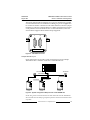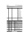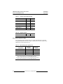
1
Instruction Bulletin
VD0C06S308
August 1996
PCMCIA Communication Card Kit
UNI-TELWAY, MODBUS/JBUS Protocols
VW3A66301U
User’s Manual
DANGER
HAZARDOUS VOLTAGE
• Read and understand this bulletin in its entirety before installing PCMCIA
card or operating ALTIVAR 66 drive controller with PCMCIA card
installed. Installation, adjustment, repair and maintenance of these drive
controllers must be performed by qualified personnel.
• Disconnect all power before servicing drive controller. WAIT ONE
MINUTE until DC bus capacitors discharge, then measure DC bus
capacitor voltage between PA and (-) terminals to verify DC voltage is
less than 45 V. The DC bus LED is not an accurate indication of the
absence of DC bus voltage.
• DO NOT short across DC bus capacitors or touch unshielded
components or terminal strip screw connections with voltage present.
• Install all covers and close door before applying power or starting and
stopping the drive controller.
• User is responsible for conforming to all applicable code requirements
with respect to grounding all equipment.
• Many parts in this drive controller, including printed wiring boards, operate
at line voltage. DO NOT TOUCH. Use only electrically insulated tools.
Before servicing drive controller:
• Disconnect all power.
• Place a “DO NOT TURN ON” label on drive controller disconnect.
• Lock disconnect in open position.
Failure to follow these instructions will result in death or serious injury.
ALTIVAR is a trademark of Telemecanique S.A. or its successor-in-interest, Schneider Electric S.A.
© 1996 Schneider S.A All rights reserved. This document may not be copied in whole or in part, or
transferred to any other media, without the written permission of Schneider S.A.
Electrical equipment should be serviced only by qualified electrical maintenance personnel. No
responsibility is assumed by Schneider S.A. for any consequences arising out of the use of this
material.
Bulletin No. VD0C06S308
August 1996
VW3A66301U PCMCIA Communication Card Kit
Table of Contents
INTRODUCTION . . . . . . . . . . . . . . . . . . . . . . . . . . . . . . . . . . . . . . . . . . . . . . . . . . . . . . . . . . . . . 1
SYSTEM SAFETY CONSIDERATIONS . . . . . . . . . . . . . . . . . . . . . . . . . . . . . . . . . . . . . 1
USING THIS MANUAL . . . . . . . . . . . . . . . . . . . . . . . . . . . . . . . . . . . . . . . . . . . . . . . . . . 2
REVISION LEVEL . . . . . . . . . . . . . . . . . . . . . . . . . . . . . . . . . . . . . . . . . . . . . . . . . . . . . . 2
SECTION 1: INSTALLATION AND CONFIGURATION . . . . . . . . . . . . . . . . . . . . . . . . . . . . . . . 3
RECEIVING . . . . . . . . . . . . . . . . . . . . . . . . . . . . . . . . . . . . . . . . . . . . . . . . . . . . . . . . . . . 3
INSTALLATION . . . . . . . . . . . . . . . . . . . . . . . . . . . . . . . . . . . . . . . . . . . . . . . . . . . . . . . . 3
Bus Voltage Measurement Procedure . . . . . . . . . . . . . . . . . . . . . . . . . . . . . . . . . . . 4
Installing the PCMCIA Communication Card Kit . . . . . . . . . . . . . . . . . . . . . . . . . . . . 7
Diagnostics . . . . . . . . . . . . . . . . . . . . . . . . . . . . . . . . . . . . . . . . . . . . . . . . . . . . . . . . 8
CONFIGURING THE COMMUNICATION FUNCTIONS. . . . . . . . . . . . . . . . . . . . . . . . . 8
First Power Up. . . . . . . . . . . . . . . . . . . . . . . . . . . . . . . . . . . . . . . . . . . . . . . . . . . . . . 8
Address . . . . . . . . . . . . . . . . . . . . . . . . . . . . . . . . . . . . . . . . . . . . . . . . . . . . . . . . . . 10
Protocol . . . . . . . . . . . . . . . . . . . . . . . . . . . . . . . . . . . . . . . . . . . . . . . . . . . . . . . . . . 10
Transmission Speed . . . . . . . . . . . . . . . . . . . . . . . . . . . . . . . . . . . . . . . . . . . . . . . . 10
Data Format . . . . . . . . . . . . . . . . . . . . . . . . . . . . . . . . . . . . . . . . . . . . . . . . . . . . . . 10
Parity . . . . . . . . . . . . . . . . . . . . . . . . . . . . . . . . . . . . . . . . . . . . . . . . . . . . . . . . . . . . 10
Forced Local . . . . . . . . . . . . . . . . . . . . . . . . . . . . . . . . . . . . . . . . . . . . . . . . . . . . . . 11
WIRING . . . . . . . . . . . . . . . . . . . . . . . . . . . . . . . . . . . . . . . . . . . . . . . . . . . . . . . . . . . . . 11
Connection to Multidrop Bus . . . . . . . . . . . . . . . . . . . . . . . . . . . . . . . . . . . . . . . . . . 12
Electrical Interface . . . . . . . . . . . . . . . . . . . . . . . . . . . . . . . . . . . . . . . . . . . . . . 12
PCMCIA Card D-Shell Electrical Interface (RS-485) . . . . . . . . . . . . . . . . . 12
PCMCIA Card D-Shell Electrical Interface (RS-232C) . . . . . . . . . . . . . . . . 13
PCMCIA Card D-Shell Electrical Interface (RS-422) . . . . . . . . . . . . . . . . . 13
Connection to UNI-TELWAY Bus with Telemecanique PLC. . . . . . . . . . . . . . . . . . 14
General . . . . . . . . . . . . . . . . . . . . . . . . . . . . . . . . . . . . . . . . . . . . . . . . . . . . . . . 14
Connection Accessories . . . . . . . . . . . . . . . . . . . . . . . . . . . . . . . . . . . . . . . . . . 14
Sample Network Layout . . . . . . . . . . . . . . . . . . . . . . . . . . . . . . . . . . . . . . . . . . 15
Connection to MODBUS Bus with MODICON PLC . . . . . . . . . . . . . . . . . . . . . . . . 16
General . . . . . . . . . . . . . . . . . . . . . . . . . . . . . . . . . . . . . . . . . . . . . . . . . . . . . . . 16
Connection Accessories . . . . . . . . . . . . . . . . . . . . . . . . . . . . . . . . . . . . . . . . . . 16
PRINCIPLE OF COMMUNICATION . . . . . . . . . . . . . . . . . . . . . . . . . . . . . . . . . . . . . . . 18
Data Structures . . . . . . . . . . . . . . . . . . . . . . . . . . . . . . . . . . . . . . . . . . . . . . . . . . . . 18
Access to Data . . . . . . . . . . . . . . . . . . . . . . . . . . . . . . . . . . . . . . . . . . . . . . . . . . . . 18
Units . . . . . . . . . . . . . . . . . . . . . . . . . . . . . . . . . . . . . . . . . . . . . . . . . . . . . . . . . . . . 18
Range . . . . . . . . . . . . . . . . . . . . . . . . . . . . . . . . . . . . . . . . . . . . . . . . . . . . . . . . . . . 18
Values at Power Up. . . . . . . . . . . . . . . . . . . . . . . . . . . . . . . . . . . . . . . . . . . . . . . . . 18
Parameter Types. . . . . . . . . . . . . . . . . . . . . . . . . . . . . . . . . . . . . . . . . . . . . . . . . . . 19
Priority of Treating Data . . . . . . . . . . . . . . . . . . . . . . . . . . . . . . . . . . . . . . . . . . . . . 19
Access Protection by Forced Local . . . . . . . . . . . . . . . . . . . . . . . . . . . . . . . . . . . . . 19
Command Mode Transitions . . . . . . . . . . . . . . . . . . . . . . . . . . . . . . . . . . . . . . . . . . 20
Serial Link Fault Protection . . . . . . . . . . . . . . . . . . . . . . . . . . . . . . . . . . . . . . . . . . . 20
Compatibility of Application Functions. . . . . . . . . . . . . . . . . . . . . . . . . . . . . . . . . . . 22
© 1996 Schneider S.A. All Rights Reserved
i
VW3A66301U PCMCIA Communication Card Kit
Table of Contents
Bulletin No. VD0C06S308
August 1996
SECTION 2: REGISTER DESCRIPTION. . . . . . . . . . . . . . . . . . . . . . . . . . . . . . . . . . . . . . . . . . 23
ADJUSTMENT WORDS (READ AND WRITE) . . . . . . . . . . . . . . . . . . . . . . . . . . . . . . . 23
COMMAND WORDS (READ AND WRITE). . . . . . . . . . . . . . . . . . . . . . . . . . . . . . . . . . 24
Freewheel and Fast Stop . . . . . . . . . . . . . . . . . . . . . . . . . . . . . . . . . . . . . . . . . . . . 25
Additional Command Register. . . . . . . . . . . . . . . . . . . . . . . . . . . . . . . . . . . . . . . . . 25
Display of Logic Input Assignments. . . . . . . . . . . . . . . . . . . . . . . . . . . . . . . . . . . . . 35
Display of Fault Register (Fault that Caused Drive Controller to Trip) . . . . . . . . . . 36
Display of Present Faults Register (Fault Present if bit = 1) . . . . . . . . . . . . . . . . . . 37
Fault History . . . . . . . . . . . . . . . . . . . . . . . . . . . . . . . . . . . . . . . . . . . . . . . . . . . . . . 38
SECTION 3: UNI-TELWAY PROTOCOL. . . . . . . . . . . . . . . . . . . . . . . . . . . . . . . . . . . . . . . . . . 39
LIST OF REQUESTS. . . . . . . . . . . . . . . . . . . . . . . . . . . . . . . . . . . . . . . . . . . . . . . . . . . 39
Identification Request . . . . . . . . . . . . . . . . . . . . . . . . . . . . . . . . . . . . . . . . . . . . . . . 39
Status Request . . . . . . . . . . . . . . . . . . . . . . . . . . . . . . . . . . . . . . . . . . . . . . . . . . . . 40
Read and Write Objects Requests . . . . . . . . . . . . . . . . . . . . . . . . . . . . . . . . . . . . . 40
Example 1: Word Object Type . . . . . . . . . . . . . . . . . . . . . . . . . . . . . . . . . . . . . 41
Example 2: Byte Object Type . . . . . . . . . . . . . . . . . . . . . . . . . . . . . . . . . . . . . . 42
Event Data. . . . . . . . . . . . . . . . . . . . . . . . . . . . . . . . . . . . . . . . . . . . . . . . . . . . . . . . 43
Specific Control Requests . . . . . . . . . . . . . . . . . . . . . . . . . . . . . . . . . . . . . . . . . . . . 43
REGISTER UPDATE TIMES . . . . . . . . . . . . . . . . . . . . . . . . . . . . . . . . . . . . . . . . . . . . . 44
SECTION 4: MODBUS PROTOCOL . . . . . . . . . . . . . . . . . . . . . . . . . . . . . . . . . . . . . . . . . . . . . 45
MODBUS FRAMES . . . . . . . . . . . . . . . . . . . . . . . . . . . . . . . . . . . . . . . . . . . . . . . . . . . . 45
PRINCIPLE OF COMMUNICATION . . . . . . . . . . . . . . . . . . . . . . . . . . . . . . . . . . . . . . . 46
Accessible Data. . . . . . . . . . . . . . . . . . . . . . . . . . . . . . . . . . . . . . . . . . . . . . . . . . . . 47
Exchanges. . . . . . . . . . . . . . . . . . . . . . . . . . . . . . . . . . . . . . . . . . . . . . . . . . . . . . . . 47
Checking and Supervision. . . . . . . . . . . . . . . . . . . . . . . . . . . . . . . . . . . . . . . . . . . . 48
MODBUS FUNCTIONS . . . . . . . . . . . . . . . . . . . . . . . . . . . . . . . . . . . . . . . . . . . . . . . . . 48
Frame Details RTU Mode . . . . . . . . . . . . . . . . . . . . . . . . . . . . . . . . . . . . . . . . . . . . 50
Read N Bits: Function 1 or 2 . . . . . . . . . . . . . . . . . . . . . . . . . . . . . . . . . . . . . . . 50
Read N Words: Function 3 or 4. . . . . . . . . . . . . . . . . . . . . . . . . . . . . . . . . . . . . 51
Write One Output Bit: Function 5 . . . . . . . . . . . . . . . . . . . . . . . . . . . . . . . . . . . 51
Write One Output Word: Function 6 . . . . . . . . . . . . . . . . . . . . . . . . . . . . . . . . . 52
Diagnostic: Function 8. . . . . . . . . . . . . . . . . . . . . . . . . . . . . . . . . . . . . . . . . . . . 52
Read Event Counter: Function 11 (H'0B') . . . . . . . . . . . . . . . . . . . . . . . . . . . . . 53
Write N Output Words: Function 16 (H'10') . . . . . . . . . . . . . . . . . . . . . . . . . . . . 53
Exception Answers . . . . . . . . . . . . . . . . . . . . . . . . . . . . . . . . . . . . . . . . . . . . . . 54
CRC16 Calculation . . . . . . . . . . . . . . . . . . . . . . . . . . . . . . . . . . . . . . . . . . . . . . 55
Frame Details ASCII Mode . . . . . . . . . . . . . . . . . . . . . . . . . . . . . . . . . . . . . . . . . . . 55
Example: Writing a value of 1 in bit B3 of drive controller 2 . . . . . . . . . . . . . . . 56
Calculation of the LRC . . . . . . . . . . . . . . . . . . . . . . . . . . . . . . . . . . . . . . . . 56
Register Update Times . . . . . . . . . . . . . . . . . . . . . . . . . . . . . . . . . . . . . . . . . . . . . . 56
APPENDIX A: ADDRESS DESCRIPTIONS & INDEX . . . . . . . . . . . . . . . . . . . . . . . . . . . . . . . 57
INDEX. . . . . . . . . . . . . . . . . . . . . . . . . . . . . . . . . . . . . . . . . . . . . . . . . . . . . . . . . . . . . . . . . . . . . 61
ii
© 1996 Schneider S.A. All Rights Reserved
VD0C06S308
August 1996
VW3A66301U PCMCIA Communication Card Kit
Introduction
INTRODUCTION
The VW3A66301U Communication Card Kit allows you to connect an
ALTIVAR 66 drive controller to multipoint networks using the following
protocols:
• UNI-TELWAY
• MODBUS RTU/JBUS
• MODBUS ASCII
The VW3A66301U Communication Card Kit consists of a Type 3 Personal
Computer Memory Card International Association (PCMCIA) card, a captive
3 m (9.84 ft) cable, and a SUB-D 15-pin connector.
The ALTIVAR 66 drive controller must be equipped with one of the following
option modules:
• I/O Extension Module VW3A66201T or VW3A66202T or
• Communication Carrier Module VW3A66205
As a node on a network, the ALTIVAR 66 drive controller can receive and
respond to data messages. The data exchange allows use of ALTIVAR 66
functions:
•
•
•
•
Downloading of adjustment parameters
Command and control
Monitoring
Diagnostics
SYSTEM SAFETY CONSIDERATIONS
WARNING
LOSS OF CONTROL
• The designer of any control scheme must consider the potential failure modes of
control paths and, for certain critical control functions, provide a means to achieve
a safe state during and after a path failure. Examples of critical control functions
are Emergency Stop and Overtravel Stop. Separate or redundant control paths
must be provided for critical control functions.
• The control paths of a system may include communication links. Consideration
must be given to the implications of unanticipated transmission delays or failures
of the link.
Failure to follow these instructions can result in death, serious injury, or
equipment damage.1
1. For additional information, refer to NEMA ICS 1.1-1984, “Safety Guidelines for the
application, Installation, and Maintenance of Solid State Control” and to NEMA
ICS7.1-1995, “Safety Standards for Construction and Guide for Selection, Installation
and Operation of Adjustable-Speed Drive Systems.”
© 1996 Schneider S.A. All Rights Reserved
1
VW3A66301U PCMCIA Communication Card Kit
Using This Manual
VD0C06S308
August 1996
USING THIS MANUAL
This manual applies to ALTIVAR 66 drive controllers equipped with software
version 3.0 or later. It consists of four sections:
• Section 1: Installation and Configuration (page 3) — describes how to
install the PCMCIA Communication Card Kit and contains wiring
information and procedures for connecting the drive controller to a UNITELWAY or MODBUS bus.
• Section 2: Register Description (page 23) — describes in detail the
ALTIVAR 66 registers, including information such as range, units and
factory settings.
• Section 3: UNI-TELWAY Protocol (page 39) — contains communication
conventions for UNI-TELWAY protocol.
• Section 4: MODBUS Protocol (page 45) — contains communication
conventions for MODBUS protocol.
Appendix A (page 57) contains a list of registers in numerical order with page
references back to the descriptions in Section 2.
For more information about specific parameters, refer to the following
ALTIVAR 66 documentation:
• Level 1 and 2 Configuration manual, VD0C06S305_
• I/O Extension Module and Level 3 Configuration manual VD0C06T306_.
Other documentation available:
• Receiving, Installation & Start-Up manual, VD0C06S304_
• Communication Carrier Module manual VD0C06N915_.
• Catalog, VD0C06S201_
Additional documentation is provided with the optional peripherals.
REVISION LEVEL
This is a new document. It is intended for use with ALTIVAR 66 drive
controllers equipped with software version 3.0 or later.
2
© 1996 Schneider S.A. All Rights Reserved
VD0C06S308
August 1996
VW3A66301U PCMCIA Communication Card Kit
Section 1: Installation and Configuration
SECTION 1: INSTALLATION AND CONFIGURATION
RECEIVING
Remove the Communication Card Kit from its packaging and visually inspect
the exterior for shipping damage. If any damage is found, notify the carrier and
your local representative. Do not install a damaged card. If the communication
card is to be stored after receipt, replace it in its original packing material and
store at -40 to +185 °F (-40 to +85 °C).
The following specifications apply to the communication interface of the
Communication Card Kit:
• Isolation (network to drive controller): Galvanically isolated for 30 V RMS,
50 V peak
• Isolation (cable jacket to ground): 300 V RMS
• Captive cable termination: 15-pin, male D-shell
• Electrical interface: RS-232, RS-422, RS-485 (selectable by connection)
INSTALLATION
WARNING
UNINTENDED EQUIPMENT ACTION
Read and understand this document, VD0C06S304_, VD0C06S305_, and the
applicable option card manual before operating the drive controller.
Failure to follow these instructions can result in death, serious injury, or
equipment damage.
Before installing, removing, or replacing the PCMCIA Communication Card
Kit, remove all power from the drive controller, including external control
power which may be present on the option module, and perform the bus
voltage measurement procedure on page 4.
© 1996 Schneider S.A. All Rights Reserved
3
VW3A66301U PCMCIA Communication Card Kit
Section 1: Installation and Configuration
VD0C06S308
August 1996
Bus Voltage Measurement Procedure
DANGER
HAZARDOUS VOLTAGE
• This product contains energy storage devices. Read and understand the Bus
Voltage Measurement Procedure before installing the PCMCIA Communication
Card Kit. Measurement of DC bus capacitor voltage must be performed by
qualified personnel.
• DC bus LED is not an accurate indication of absence of DC bus voltage.
• DO NOT short across capacitors or touch unshielded components or terminal strip
screw connections with voltage present.
• Many parts in this drive controller, including printed wiring boards, operate at line
voltage. DO NOT TOUCH. Use only electrically insulated tools.
Failure to follow these instructions will cause shock or burn, resulting in death
or serious injury.
The PA and - terminals are located inside the drive controller (see Figure 1). To
measure bus capacitor voltage:
1.
2.
3.
4.
Disconnect all power from the drive controller.
Wait 1 minute to allow the DC bus to discharge.
Open the front cover of the drive controller.
Set the voltmeter to the 1000 VDC scale. Measure the bus capacitor voltage
between the PA and - terminals to verify that the DC voltage is less than
45 V. Do not short across capacitor terminals with voltage present!
5. If the bus capacitors are not fully discharged, contact your local
representative. Do do not operate the drive controller.
4
© 1996 Schneider S.A. All Rights Reserved
VD0C06S308
August 1996
VW3A66301U PCMCIA Communication Card Kit
Section 1: Installation and Configuration
DC Bus
LED
AI2-U
AI2-I
—
PA
ATV66U41N4 to D12N4 and
ATV66U41M2 to U90M2
F4
DC Bus
LED
DC Bus
LED
AI2-U
AI2-I
AI2-U
AI2-I
J13
Protective
Switch
(GV2)
J12
J2
—
ATV66D16N4 to D79N4 and
ATV66D12M2 to D46M2
Figure 1:
—
PA
PA
ATV66C10N4 to C19N4
Location of PA and - Terminals: ATV66U41N4 to C19N4 and
ATV66U41M2 to D46M2
© 1996 Schneider S.A. All Rights Reserved
5
VW3A66301U PCMCIA Communication Card Kit
Section 1: Installation and Configuration
PA
L1
PB
VD0C06S308
August 1996
L3
L2
PA
–
—
DC Bus
LED
F4A
Figure 2:
6
F4B
F4C
Location of PA and - Terminals: ATV66C23N41 to C31N41
© 1996 Schneider S.A. All Rights Reserved
VD0C06S308
August 1996
VW3A66301U PCMCIA Communication Card Kit
Section 1: Installation and Configuration
Installing the PCMCIA Communication Card Kit
To install the PCMCIA Communication Card Kit into drive controller:
1. Open the drive controller door.
2. On models ATV66U41N4 to D23N4 and ATV66U41M2 to U90M2, remove
plastic knockout from top of drive controller cover.
NOTE: The drive controller enclosure Type rating will change from Type 1 to
Open when the knockout is removed.
3. Insert the PCMCIA card 68-pin connector into the PCMCIA slot on top of
option card with the “Insert” arrows facing towards the front of drive
controller (see Figure 3).
4. For models ATV66U41N4 to D12N4 and ATV66U41M2 to U90M2: the
PCMCIA captive cable must be routed through the knockout and outside
the drive controller enclosure. For all other models, route the captive cable
inside the drive controller enclosure, along with the control conductors
connected to J12 and J13 of the drive controller main control board.
NOTE: The 15-pin D-shell connector of the PCMCIA captive cable has exposed
metal parts. The cable must be routed and anchored so that the connector avoids
contact with live conductors within the drive controller.
5. For models ATV66D16N4 to D79N4 and ATV66D12M2 to D46M2:
provisions in the bottom plastic plate allow the PCMCIA captive cable
connector to exit through the bottom of the drive controller enclosure.
NOTE: If the captive cable and connector of the PCMCIA card exit the drive
controller enclosure, additional mechanical and environmental protection of the
cable and connector may be required.
Plastic
Knockout
Figure 3:
SQUARE D
To remove the
Communication
Card Kit, push
eject button on
option card
Mounting and Removing PCMCIA Communication Card Kit
© 1996 Schneider S.A. All Rights Reserved
7
VW3A66301U PCMCIA Communication Card Kit
Section 1: Installation and Configuration
VD0C06S308
August 1996
Diagnostics
There are two LEDs on top of the PCMCIA interface card: a green “COM” LED
and a red “ERR” LED. Status is indicated when the LEDs flash the patterns
described in Figure 4.
Green
COM LED
ERR
Red ERR
LED
Illuminated
Off
Normal operation
Flashing
Off
• Incorrect
communication
configuration
• ALTIVAR 66
communication fault
COM
Figure 4:
Probable Causes
Corrective Action
• Check configuration
• Check software compatibility
Off
Illuminated Communication fault on • Check the switch positions on the
the bus
TSX-SCA62 connector, if present.
• Check for presence of master
device and its proper link,
configuration, and operation.
Off
Off
PCMCIA card or drive
controller fault
Check the drive controller by
removing the PCMCIA card.
Replace the drive controller or the
card.
PCMCIA LEDs — LED Status Indication
CONFIGURING THE COMMUNICATION FUNCTIONS
First Power Up
For a good understanding of access to the different menus, see the Level 1 & 2
Configuration manual, VD0C06S305_, and (if an I/O Extension Module is
installed) the I/O Extension Module & Level 3 Configuration manual,
VD0C06T306_.
OPT.:VW3A66205
English
INSTALLED.
REMEMBER YOU NEED TO
CONFIGURE THE OPTION
ENT to continue
Figure 5:
8
At first power up, a message appears on the
keypad display to allow identification of the
option. After OPT, the catalog number of the
selected card is shown. Press ENT. This will
reconfigure the drive controller to factory
settings.
First Power Up
© 1996 Schneider S.A. All Rights Reserved
VD0C06S308
August 1996
VW3A66301U PCMCIA Communication Card Kit
Section 1: Installation and Configuration
WARNING
UNINTENDED EQUIPMENT OPERATION
• Installation of an option module will reset all drive controller parameters, including
I/O assignments, to factory default settings.
• Before installing an option module, record all existing settings of the drive
controller.
• After installing the option module, reset drive controller back to recorded values.
Failure to follow these instructions can result in death or serious injury.
In the Drive Identification menu, you can check
the catalog number of the option installed by
pressing the ▲▼ keys.
DRIVE IDENTIFICATION
ATV66U41N4 CT V3.0
POWER :2.2kW/3HP
In=5.8A Imax=1.5In
SUPPLY :400-415V
ENT to continue
OPT.1:VW3A66205V
Figure 6:
Drive Identification
FAULT
OPT: VW3A66205
EIS NOT RECOGNIZED
OR
HAS BEEN REMOVED
ENT to continue
ESC
When the drive controller is powered up, if the
option has been removed after being configured,
the fault screen appears. The option must be
reinstalled, or the drive controller settings must
be reset to factory preset values.
ENT
or 20 s
TO RESET FAULT
YOU NEED TO REINSTALL
OPT: VW3A66205
OR INITIALIZE DRIVE
TO FACTORY SETTINGS
ENT to initialize
Figure 7:
Fault Screen
Select the 11→Communication menu to access
the configuration parameters of the PCMCIA
Communication Card Kit. This menu contains
four submenus for configuring protocol,
transmission speed, network format, and
parity. Drive address is entered directly on the
Communication menu from the keypad.
11- COMMUNICATION
ADDRESS
:
0
PROTOCOL :
--TRAN.SPEED:
9.6
FORMAT
:8B,1 stop
PARITY
:
ODD
Figure 8:
Communication Menu
© 1996 Schneider S.A. All Rights Reserved
9
VW3A66301U PCMCIA Communication Card Kit
Section 1: Installation and Configuration
VD0C06S308
August 1996
Address
The address varies with the protocol selected and is configurable. Factory
setting is 0. Maximum value is 31.
Protocol
The VW3A66301U PCMCIA Communication
Card Kit supports three protocols:
--UNI-TELWAY
Modbus RTU
Modbus ASC
Figure 9:
•UNI-TELWAY
•MODBUS RTU
•MODBUS ASCII
Protocol Menu
Factory setting is – – – (no protocol selected). Select the protocol appropriate for
your network.
Transmission Speed
Network transmission speed is selectable from
300 to 19,200 baud. The factory preset
transmission speed is 9,600 baud.
0.3
0.6
1.2
2.4
4.8
9.6
19.2
Figure 10: Transmission Speed Menu
Data Format
7b
7b
8b
8b
1
2
1
2
Depending on protocol selected, one or both of
the following data formats are available:
stop
stop
stop
stop
•7 bits with 1 or 2 stop bits (MODBUS ASCII only)
•8 bits with 1 or 2 stop bits
Factory setting is 8 bits with 1 stop bit.
Figure 11: Data Format Menu
Parity
Set parity as none, even or odd. Factory setting is
odd.
NON
ODD
EVEN
Figure 12: Parity Menu
10
© 1996 Schneider S.A. All Rights Reserved
VD0C06S308
August 1996
VW3A66301U PCMCIA Communication Card Kit
Section 1: Installation and Configuration
Forced Local
F0RCED LOCAL
NO
YES,LOGIC IN:___
†,™ & ENT to modify
ESC to quit
A forced local logic input can be defined in the
7.2→Application Functions menu. This logic
input returns control to the terminal strip or
keypad if in Serial Link Command Mode
(W2020, 1 [DLI] and W2020, 2 [FLI] set to 1; see
page 24.)
Figure 13: Forced Local Menu
Forced local can also be selected in the 5→Keypad Configuration menu and
assigned to the F1 function key. The F1 function key can be used to toggle
between Local (Keypad or Terminal Command, depending on the setting of
T/K) and Remote (Serial Link Command).
WIRING
WARNING
LOSS OF CONTROL
• The designer of any control scheme must consider the potential failure modes of
control paths and, for certain critical control functions, provide a means to achieve
a safe state during and after a path failure. Examples of critical control functions
are Emergency Stop and Overtravel Stop. Separate or redundant control paths
must be provided for critical control functions.
• The control paths of a system may include communication links. Consideration
must be given to the implications of unanticipated transmission delays or failures
of the link.
Failure to follow these instructions can result in death, serious injury, or
equipment damage.1
1. For additional information, refer to NEMA ICS 1.1-1984, “Safety Guidelines for the
application, Installation, and Maintenance of Solid State Control” and to NEMA
ICS7.1-1995, “Safety Standards for Construction and Guide for Selection, Installation
and Operation of Adjustable-Speed Drive Systems.”
© 1996 Schneider S.A. All Rights Reserved
11
VW3A66301U PCMCIA Communication Card Kit
Section 1: Installation and Configuration
VD0C06S308
August 1996
Connection to Multidrop Bus
Electrical Interface
The electrical interface of the VW3A66301U PCMCIA Communication Card Kit
is selectable as either RS-485, RS-422, or RS-232C.
5V
4.7 kΩ
TX
Send
Validation
0V
D (B)
E
D (A)
5
15
14
External View of PCMCIA
Communication Card Kit
Connector
7
4.7 kΩ
&
8
0V
7
6
15
14
13
5
5V
100 kΩ
RX
12
4
11
RD (B)
&
100 kΩ
0V
RD (A)
2
3
8
3
10
2
1
9
0V
Figure 14: Electrical Interface
The electrical interface is isolated from the drive controller. It is supplied on a
Sub D 15-pin connector. Figure 15 illustrates the RS-485 interface (seen from the
external contact side), Figure 16 illustrates the RS-232C interface, and Figure 17
illustrates the RS-422 interface.
PCMCIA Card D-Shell Electrical Interface (RS-485)
0 V 15
D (B) 14
D (A) 7
Figure 15: RS-485 Interface
12
© 1996 Schneider S.A. All Rights Reserved
VD0C06S308
August 1996
VW3A66301U PCMCIA Communication Card Kit
Section 1: Installation and Configuration
PCMCIA Card D-Shell Electrical Interface (RS-232C)
5
15
14
TX
7
2
SG
3
RX
8
NOTE: Shield connected to ground at other end
Figure 16: RS-232C Interface
PCMCIA Card D-Shell Electrical Interface (RS-422)
0 V 15
D (B) 14
D (A) 7
OR
RD (B) 3
RD (A) 8
Figure 17: RS-422 Interface
© 1996 Schneider S.A. All Rights Reserved
13
VW3A66301U PCMCIA Communication Card Kit
Section 1: Installation and Configuration
VD0C06S308
August 1996
When wiring ALTIVAR 66 drive controllers equipped with PCMCIA
communication cards to a multidrop bus, follow the wiring practices required
by national and local electrical codes in addition to the following:
• Use metallic conduit for all drive controller wiring. Do not run multidrop
cable and power wiring in the same conduit.
• Metallic conduit carrying power wiring must be separated from metallic
conduit containing the multidrop cable by at least 8 cm (3 in).
• Non-metallic conduit or cable trays used to carry power wiring must be
separated from metallic conduit containing multidrop cable by at least
30.5 cm (12 in).
• Whenever power wiring and multidrop cable cross, the metallic conduit
and non-metallic conduit or trays must cross at right angles.
• For the multidrop cable, use shielded cable with one or two pairs of twisted
conductors. Use the cable recommended for each multidrop bus system
shown.
• Connect the multidrop cable shield as shown in Figure 15, 16, or 17, in
order to equalize the voltage potential at each PCMCIA Communication
Card. Ground the shield only at one point.
• The maximum total cable length allowed is 1,000 m (3,281 ft).
Connection to UNI-TELWAY Bus with Telemecanique PLC
General
You must follow these rules when constructing a UNI-TELWAY multidrop
network:
• Limit the number of nodes on the network to 28.
• Limit the stub cable length at each junction to 20 m (66 ft).
• Terminate each end of each twisted pair of the multidrop cable as shown
in Figure 18.
120 Ω
1 nF
Figure 18: Zt Termination Device
Connection Accessories
To facilitate connection of the drive controller to the multidrop bus, the
following accessories are available from the Telemecanique catalog.
Cable for connections to the bus is supplied in 3 different lengths:
• TSX-CSA 100: length 100 m (328 ft)
• TSX-CSA 200: length 200 m (656 ft)
• TSX-CSA 500: length 500 m (1,640 ft)
14
© 1996 Schneider S.A. All Rights Reserved
VD0C06S308
August 1996
VW3A66301U PCMCIA Communication Card Kit
Section 1: Installation and Configuration
The TSX-SCA62 terminal block (Figure 19) is a passive unit featuring a printed
circuit board fitted with screw terminals for enabling two pieces of equipment to
be connected to the bus. It includes an end-of-line terminator, which is a jumper
inside the box. The drive controller address is coded by setting the microswitches
on the printed circuit board inside the box. For more information, refer to the
documentation shipped with the Telemecanique equipment.
1
2
Figure 19: TSX-SCA62 Connector
Sample Network Layout
Figure 20 illustrates one possible system configuration involving multiple
ALTIVAR 66 drive controllers connected to a UNI-TELWAY bus.
TSX-SCM 21.6
TSX-CSB015
TSX-SCA62
TSX-CSAXXX
VW3-A66301
ATV66
VW3-A66205 or
VW3-A66201T
VW3-A66202T
ATV66
ATV66
Figure 20: System Configuration: Multiple Drives on UNI-TELWAY Bus
NOTE: The ground connections between the TSX-SCA62 box and the ALTIVAR 66
drive controller must be made for good system operation. Connections should be as short
as possible.
© 1996 Schneider S.A. All Rights Reserved
15
VW3A66301U PCMCIA Communication Card Kit
Section 1: Installation and Configuration
VD0C06S308
August 1996
Connection to MODBUS Bus with MODICON PLC
General
You must follow these rules when constructing a MODBUS multidrop network:
• Limit the number of nodes on the network to 32.
• Daisy-chain the multidrop cable as illustrated in Figure 21. Do not use stub
connections.
Connection Accessories
Many Modicon PLCs cannot initiate messages from a MODBUS port because
they were intended to be used as slave devices only. Therefore, when using a
Modicon PLC, the Modicon BM85 Bridge Mux must be connected to the
MODBUS Plus port. For multiple drives, a Telemecanique TSX-SCA 72 RS-232C
to RS-485 converter must be used. Figure 21 shows system configuration
involving multiple ALTIVAR 66 drive controllers connected to a MODBUS bus,
using a Modicon PLC.
NOTE: Your MODBUS device or PLC may be capable of initiating a message directly
from a MODBUS port (it must be a master port). Consult Modicon for more
information if this is the case.
16
© 1996 Schneider S.A. All Rights Reserved
VD0C06S308
August 1996
VW3A66301U PCMCIA Communication Card Kit
Section 1: Installation and Configuration
MODICON PLC
I/O
CPU
I/O
I/O
MB SLAVE PORT
MB SLAVE PORT
MB+ PORT
RS-485
ModBus+
MB+ ADDRESS 10
RS-485
WIRING
INTERFACE *
Modicon BM85
Bridge-Mux
2
4
1
3
1
2
3
4
5
6
Telemecanique
TSX-SCA72
RS232 to RS485
D(A) D(B) 0V
1 2 3 4 5
WHT/
BLU
WHT/
BLU
BLU/
WHT
BLU/
WHT
WIRING
INTERFACE *
1
2
3
WHT/
BLU
BLU/
WHT
7 D (A)
8
9
10
11
12
13
14 D (B)
15 0 V
G
G
DRIVE 5
DRIVE SLAVE ADDRESS 5
ROUTE ADDRESS 10:4:5
WIRING INTERFACE *
4
5
6
1
2
3
7 D (A)
8
9
10
4
5
6
7 D (A)
8
9
10
WHT/BLU
DRIVE 4
11
12
13
14 D (B)
15 0 V
G
G
BLU/WHT
* WIRING INTERFACE: TELEMECANIQUE ABE-6SD15F OR WAGO 810-289/W02
CABLE: BELDEN 9841 OR EQUIVALENT
DRIVE n
11
12
13
14 D (B)
15 0 V
G
G
NOTE: GROUND SHIELD ONLY AT PIN 5 OF THE TSX-SCA72
Figure 21: MODBUS Network Diagram
© 1996 Schneider S.A. All Rights Reserved
17
VW3A66301U PCMCIA Communication Card Kit
Section 1: Installation and Configuration
VD0C06S308
August 1996
PRINCIPLE OF COMMUNICATION
Data Structures
ALTIVAR 66 drive controllers are adjusted, controlled and monitored through
data stored in drive controller memory. The data consists of bits and words.
Words consist of 16 bits and are designated Wx, where x indicates word number.
Words are used for saving either numerical values (e.g., -32768 to +32767) or 16
independent logic states. The latter are also called registers.
For example, W2021 saves a numerical value for frequency reference and W2040
is a register consisting of 16 state bits. The notation W2040,2 designates bit 2 of
register W2040.
Access to Data
The tables in Section 2 “Register Description” (pages 23-38) list drive controller
parameters accessible by communication. The exact function of each parameter
and how it affects drive controller operation are explained in instruction
bulletins VD0C06S305_ and VD0C06T306_.
Data such as fault and monitoring information can only be read. Any attempt to
write to this data will be refused. The bits and words corresponding to the
adjustment, frequency reference, and command of the drive controller can be
written to as well as read.
Units
Words are always expressed in signed (-32768 to +32767) or unsigned (0 to
65535) units. In the tables in Section 2 (pages 23-38), the units of each word are
shown. For example, W2002 (Acceleration 1 time) is in units of 0.1 seconds.
Therefore, a value of 60 corresponds to an acceleration time of 6 s.
Range
The allowable range is specified for each parameter. If a value outside of the
range is written, the parameter will be set either to the range limit or to the
factory default value.
Values at Power Up
At each power up, the ALTIVAR 66 drive controller is initialized with the
configuration and adjustments saved in its EEPROM. W2021 and all of the bits
in W2020 and W2031 are set to 0 and W2024 and W2028 are set to their factory
default values. Also at power up, the drive controller is systematically placed in
Local command (terminal strip or keypad command). To control via a
multipoint bus, you must set the drive controller to Serial Link command by
setting W2020,1 (DLI) and W2020,2 (FLI) to 1. See pages 24 and 25 for more
information on these registers.
18
© 1996 Schneider S.A. All Rights Reserved
VD0C06S308
August 1996
VW3A66301U PCMCIA Communication Card Kit
Section 1: Installation and Configuration
Parameter Types
There are several different types of parameters:
• Adjustment parameters — can be written and read while the drive
controller is running or stopped.
• Command parameters — used to enable and disable Serial Link Command
mode, start and stop the drive controller, and command the general
operation of the drive controller.
• Display parameters — read-only parameters for monitoring.
Table 1 shows which adjustment parameters are available as a function of
Control Type.
Table 1:
Adjustment Parameter Setting Menu
Variable Torque or Variable
Torque Low Noise
Constant Torque
Normal
High Torque
Special
Normal
NOLD
Low Speed
Low Speed
Low Speed
Low Speed
Low Speed
High Speed
High Speed
High Speed
High Speed
High Speed
Acceleration
Acceleration
Acceleration
Acceleration
Acceleration
Deceleration
Deceleration
Deceleration
Deceleration
Deceleration
Acceleration 2 [1]
Acceleration 2 [1]
Acceleration 2 [1]
Acceleration 2 [1] Acceleration 2 [1]
Deceleration 2 [1]
Deceleration 2 [1]
Deceleration 2 [1]
Deceleration 2 [1] Deceleration 2 [1]
Damping
Damping
Damping
Damping
Damping
Motor Overload
Motor Overload
Motor Overload
Motor Overload
Motor Overload
Slip Compensation [2]
Slip Compensation [2]
Slip Compensation [2]
Profile
IR Compensation
IR Compensation
IR Compensation
Voltage Boost
Voltage Boost
Bandwidth
[1]
[2]
Only effective if Alternate Ramps has been selected via the keypad or PC software.
Only effective if Slip Compensation has been set to Manual via the keypad or PC software.
Priority of Treating Data
When several types of parameters are written in the same request, they are
treated in the following order:
1. Writing bits W2020,1 and W2020,2 (DLI and FLI) to 1
2. Adjustment parameters
3. Command parameters (except W2020,1 and W2020,2)
Access Protection by Forced Local
All writing is blocked during Forced Local.
© 1996 Schneider S.A. All Rights Reserved
19
VW3A66301U PCMCIA Communication Card Kit
Section 1: Installation and Configuration
VD0C06S308
August 1996
Command Mode Transitions
Wire the drive controller as shown in the Receiving, Installation, and Start-Up
manual (VD0C06S304_). When transitioning between Serial Link command,
Terminal strip command, and Keypad command, the drive controller behaves
as shown in Table 2. There are two ways to transition between states: by a
change in state of Forced Local (by logic input or keypad function key), or by a
change in state of the DLI/FLI bits in W2020.
Table 2:
Transition Between Command States
DLI/
FLI
0
0
0
0
1
1
1
1
SLC
Run
0
0
1
1
0
0
1
1
0
1
0
1
0
1
0
1
SLC
(Stop)
Not
Possible
SLC
(Run)
Not
Possible
DLI/
FLI
SLC
Run
Forced
Local
0
0
0
0
0
1
No
Change
0
1
0
No
Not
Change Possible
0
1
1
Not
No
No
Possible Change Change
1
0
0
Local 2
1
0
1
Not
No
Not
No
Possible Change Possible Change
SLC
(Stop)
1
1
0
Local 1
Not
Not
Local 1
Possible
Possible
SLC
(Stop)
1
1
1
Not
No
Not
No
Not
No
SLC
Possible Change Possible Change Possible Change (Run)[1]
[1]
No
No
Not
Change Change Possible
Not
No
Not
No
Not
No
Possible Change Possible Change Possible Change
No
Change
SLC
(Stop)
Not
Possible
SLC
(Run)
Not
Possible
Not
No
Not
No
Possible Change Possible Change
Not
Not
Local 2
Possible
Possible
Local 2
SLC
(Run)
Not
Possible
Not
No
Possible Change
Not
Possible
Local 2
Local Command mode speed and direction are copied to W2021 and W2040,9 respectively.
SLC:
Serial Link Command
Local 1: When transferring to Keypad command mode, the drive controller stops. When transferring to
Terminal command mode, the drive controller stops unless a terminal command is present (direction
and speed coming from the terminal strip).
Local 2:When transferring to Keypad command mode, there is no change in the drive controller state. When
transferring to Terminal command mode, the drive controller stops unless a terminal command is
present (direction and speed coming from the terminal strip).
Serial Link Fault Protection
The PCMCIA communication card continuously monitors the status of the
serial link messaging while in Serial Link Command mode. This is in addition
to the diagnostic checks described on page 8. The PCMCIA card must see a
communication to the drive controller at least every 10 seconds or a
communication fault will result.
20
© 1996 Schneider S.A. All Rights Reserved
VD0C06S308
August 1996
VW3A66301U PCMCIA Communication Card Kit
Section 1: Installation and Configuration
WARNING
LOSS OF CONTROL
Setting W2020,4 (NTO) to 1 disables serial link fault protection. Provide alternate
control paths when disabling the serial link fault protection.
Disabling the serial link fault protection can result in loss of control and can
result in death, serious injury, or equipment damage.
If W2020,4 is set to 1, the PCMCIA communication card will not monitor the
frequency of the messaging on the serial link. Operation with 2020,4 set to 1 is
useful during certain diagnostic and commissioning procedures. W2020,4
should be set to 0 for normal Serial Link Command mode operation.
WARNING
LOSS OF CONTROL
• The designer of any control scheme must consider the potential failure modes of
control paths and, for certain critical control functions, provide a means to achieve
a safe state during and after a path failure. Examples of critical control functions
are Emergency Stop and Overtravel Stop. Separate or redundant control paths
must be provided for critical control functions.
• The control paths of a system may include communication links. Consideration
must be given to the implications of unanticipated transmission delays or failures
of the link.
Failure to follow these instructions can result in death, serious injury, or
equipment damage.1
1. For additional information, refer to NEMA ICS 1.1-1984, “Safety Guidelines for the
application, Installation, and Maintenance of Solid State Control” and to NEMA
ICS7.1-1995, “Safety Standards for Construction and Guide for Selection, Installation
and Operation of Adjustable-Speed Drive Systems.”
© 1996 Schneider S.A. All Rights Reserved
21
VW3A66301U PCMCIA Communication Card Kit
Section 1: Installation and Configuration
VD0C06S308
August 1996
Compatibility of Application Functions
Some Local Command mode (keypad or terminal strip) functions, as well as
certain application functions of the ALTIVAR 66 drive controller, are not active
in Serial Link Command mode. Table 3 shows which functions are active in
Serial Link Command mode.
Table 3:
Compatibility of Application Functions
Function programmed in Local
Command mode
22
Active in Serial Link
Command mode
Stop (Run Enable)
Yes
Run Forward
No
Run Reverse
No
Jog
No
+Speed/-Speed
No
Setpoint Memory
No
Preset Speeds
No
Speed Reference
No
Auto/Manual
No
Controlled Stop by LI
No
Controlled Stop by Freq.
Yes
Shutdown
Yes
Bypass
Yes
Brake Sequence
Yes
Cycles
No
Orient
No
Forced Local
Yes
Current Limit by LI
No
Voltage Reduction by LI
No
© 1996 Schneider S.A. All Rights Reserved
VD0C06S308
August 1996
VW3A66301 PCMCIA Communication Card Kit
Section 2: Register Description
SECTION 2: REGISTER DESCRIPTION
WARNING
UNINTENDED EQUIPMENT ACTION
• Writing to registers that are designated as reserved may cause unintended
equipment operation.
• DO NOT write data to registers unless the function to be performed is completely
understood. Consult the appropriate drive controller manual for additional details.
Failure to follow these instructions can result in death, serious injury, or
equipment damage.
ADJUSTMENT WORDS (Read and Write)
These parameters can be adjusted when the motor is stopped or running.
Word
Range
Units
Description
Factory Setting
W2000 W2001 to Max. Freq.
0.1 Hz High speed
(set via keypad in Menu
7.12 or PC software)
50 Hz for 50 Hz input power
60 Hz for 60 Hz input power
W2001 0 to W2000
0.1 Hz Low speed
0 Hz
W2002 1 to 9999
0.1 s
Accel 1
3s
W2003 1 to 9999
0.1 s
Decel 1
3s
W2004 1 to 9999
0.1 s
Accel 2 [1]
5s
W2005 1 to 9999
0.1 s
Decel 2 [1]
5s
W2006 1 to 100
0.1 Hz Slip compensation [2]
3 Hz
1%
IR compensation
100%
1%
Profile
20%
W2007 0 to
800 [3]
W2008 0 to 100
W2009 0 to 100
1%
Voltage boost
20%
W2010 0 to 800 [3]
1%
Damping
20%
W2011 0 to 100
0.1%
Bandwidth
20%
W2012 45% In to 115% In
0.1 A
Motor overload
0.9 x In
[1]
These registers are only effective if Alternate Ramps has been selected via the keypad or PC software.
[2]
This register is only effective if Slip Compensation has been set to Manual via the keypad or PC software.
[3]
Depends on torque type: High torque = 150; Special = 800; Other = 100.
© 1996 Schneider S.A. All Rights Reserved
23
VW3A66301 PCMCIA Communication Card Kit
Section 2: Register Description
VD0C06S308
August 1996
COMMAND WORDS (Read and Write)
Word
W2020
Description
Drive reset
Possible Values
W2020,0 = 0 No reset
W2020,0 = 1 Reset (must be in Serial Link
Command [SLC] mode for reset to take effect)
W2020,1 = 0 No logic commands over link
Assignment of logic commands
W2020,1 = 1 Logic commands over link
over link (DLI) [1]
Assignment of references over link W2020,2 = 0 No references over link
(FLI) [1]
W2020,2 = 1 References over link
Alternate ramps (Ramp 2)
W2020,3 = 0 Ramp 1
W2020,3 = 1 Ramp 2
WARNING
LOSS OF CONTROL
Setting W2020,4 (NTO) to 1 disables serial link fault protection. Provide
alternate control paths when disabling the serial link fault protection.
Disabling the serial link fault protection can result in loss of control and
can result in death, serious injury, or equipment damage.
Suppression of communication
control (NTO)
W2020,4 = 0 Monitor communication fault
W2020,4 = 1 Do not monitor communication
fault (no time-out)
Run/Stop command [2]
W2020,5 = 0 Stop
W2020,5 = 1 Run
W2020,6 = 0 No command to inject DC
W2020,6 = 1 Command to inject DC
W2020,7
W2020,8 See table below
W2020,9 See table below
W2020,10
W2020,11
W2020,12
W2020,13
W2020,14 = 0 No external fault
W2020,14 = 1 External fault present [3]
Braking by DC injection (DCB)
Reserved
Freewheel stop
Fast stop
Reserved
Reserved
Reserved
Reserved
Command of external fault (EFL)
[1]
Split control via DLI and FLI is not available. Setting only one bit active will cause the drive controller to
set both bits active. Always write both bits to the same state.
Note: for operation in Serial Link Command (SLC) mode, both DLI and FLI must be set to 1 and LI1 must
be active.
[2]
Simultaneously writing W2020, 1, W2020,2 and W2020,5 to zero while the drive controller is running in
SLC mode will transfer control to Local Command mode (either terminal or keypad). The drive controller
will respond as indicated in Table 2 on page 20. However W2020,5 will remain active.
[3]
Allows drive controller to fault upon external fault when in SLC mode when LIx is set for customer fault.
If W2020,14 = 0, the drive controller ignores LIx, even if LIx was configured in Local Command mode
(Keypad or Terminal strip).
24
© 1996 Schneider S.A. All Rights Reserved
VD0C06S308
August 1996
VW3A66301 PCMCIA Communication Card Kit
Section 2: Register Description
Freewheel and Fast Stop
Freewheel Stop
W2020,8
0
1
1
0
Fast Stop
W2020,9
0
1
0
1
Stop Type
Normal stop
Freewheel stop
Freewheel stop
Fast stop
COMMAND WORDS (Read and Write)
Additional Command Register
Word
Description
Possible Values
W2031
Reserved
W2031,0
Run direction
W2031,1 = 0 Forward
W2031,1 = 1 Reverse
Reserved
W2031,2
Word
Range
Description
W2021
-32767 to
32767
Reference frequency 26478 = 400 Hz
-26478 = -400 Hz
Loss of all power to drive controller [1] resets
W2021 to factory default of 0 (0 Hz).
W2024
40 to
150%
% of current limit
% of motor In
(1% steps)
W2028
20 to
100%
% of voltage
Value is valid only when in SLC mode. Loss
reduction (1% steps) of all power to drive controller [1] resets
W2028 to factory default of 100%.
[1]
Remarks
Value is valid only when in SLC mode. Loss
of all power to drive controller [1] resets
W2024 to factory default of 150% (CT @
60 Hz), 135% (CT @ 50 Hz), or 110% (VT).
Control logic inactive, green LED on front of drive controller Off.
© 1996 Schneider S.A. All Rights Reserved
25
VW3A66301 PCMCIA Communication Card Kit
Section 2: Register Description
VD0C06S308
August 1996
DISPLAY WORDS (Read Only)
Word
Range
Units
Description
Possible Values
W2044
0 to 100
1%
Value of analog input AI1
0% for 0 V and 100% for 10 V
W2063
0 to 100
1%
Value of analog input AI2
0% for 0 mA and 100% for 20 mA
W2064
0 to 100
1%
Value of analog input AI3
0% for 0 V and 100% for 10 V
W2065
0 to 100
1%
Value of analog input AI4
0% for 0 mA and 100% for 20 mA
W2100
Assignment of AI1
= 0 Not assigned
= 1 Current limit
= 2 Voltage reduction
= 3 Speed Ref. 1 [1]
= 4 Speed Ref. 2
= 5 Speed Ref. 3
W2101
Assignment of AI2
= 0 Not assigned
= 1 Current limit
= 2 Voltage reduction
= 3 Speed Ref. 1
= 4 Speed Ref. 2 [1]
= 5 Speed Ref. 3
W2102
Assignment of AI3
= 0 Not assigned [1]
= 1 Current limit
= 2 Voltage reduction
= 3 Speed Ref. 1
= 4 Speed Ref. 2
= 5 Speed Ref. 3
= 6 Tach feedback
W2103
Assignment of AI4
= 0 Not assigned [1]
= 1 Current limit
= 2 Voltage reduction
= 3 Speed Ref. 1
= 4 Speed Ref. 2
= 5 Speed Ref. 3
[1]
26
Factory setting.
© 1996 Schneider S.A. All Rights Reserved
VD0C06S308
August 1996
VW3A66301 PCMCIA Communication Card Kit
Section 2: Register Description
DISPLAY WORDS (Read Only)
Word
Range
W2052
Units
0.1 kW
Description
Remarks /
Possible Values
Output power
Function of hp
W2053
0 to Nominal motor 1 V
voltage
Output voltage
Function of drive
controller voltage range
W2054
0 to Max. [1]
1V
Mains voltage
Function of drive
controller voltage range
W2055
0 to Max. [2]
1V
Bus voltage
Function of drive
controller voltage range
W2071
0 to 3
Nominal motor voltage
range
= 0 208–240 V
= 1 380–415 V
= 2 440–460 V
W2202
0 to 3
Drive controller voltage
range
= 0 Not used
= 1 208–240 V
= 2 380–460 V
W2056
0 to 199
1%
Motor thermal state value
W2057
0 to 125
1%
Drive controller thermal
state value
For kW > 7.5 kW
[1]
Maximum depends on mains: 264 V for ATV66•••M2; 460 V for 50 Hz mains (ATV66•••N4);
529 V for 60 Hz mains (ATV66•••N4).
[2]
Maximum depends on mains: 374 V for ATV66•••M2; 651 V for 50 Hz mains (ATV66•••N4);
748 V for 60 Hz mains (ATV66•••N4).
Word
Range
Unit
W2203
W2041
-26478 to 26478
Description
Remarks /
Possible Values
Mains frequency
recognized
= 0 Unknown
= 1 50 Hz
= 2 60 Hz
Output frequency
400 Hz = 26478
W2205
0.1 A
Drive controller nominal
current
Function of hp, mains
voltage, and torque type
W2206
0.1 A
Drive controller maximum
current
Function of hp, mains
voltage, and torque type
W2042
0.1 A
Output current
Function of hp and
mains voltage
© 1996 Schneider S.A. All Rights Reserved
27
VW3A66301 PCMCIA Communication Card Kit
Section 2: Register Description
VD0C06S308
August 1996
DISPLAY WORDS (Read Only)
Word
Description
Possible Values
W2040
Mode in which all
commands are assigned
W2040,0 = 0 Commands assigned by link (SLC mode)
W2040,0 = 1 Commands assigned by terminal or keypad
(local mode)
Drive controller ready
(RDY or SLC)
W2040,1 = 0 Drive controller not ready
W2040,1 = 1 Drive controller ready
Fault (FLT)
W2040,2 = 0 No fault
W2040,2 = 1 Drive controller faulted
Reset authorized
W2040,3 = 0 Reset not authorized
W2040,3 = 1 Reset authorized
Brake engage relay state
W2040,4 = 0 Brake set (relay deenergized)
W2040,4 = 1 Brake released (relay energized)
Forced local
W2040,5 = 0 Drive controller not forced to local
W2040,5 = 1 Drive controller forced to local
NTO
W2040,6 = 0 Time-out fault
W2040,6 = 1 No time-out fault
Resettable fault
W2040,7 = 0 Non-resettable fault
W2040,7 = 1 Resettable fault
Motor running
W2040,8 = 0 Motor stopped
W2040,8 = 1 Motor running
Actual rotation direction
W2040,9 = 0 Forward
W2040,9 = 1 Reverse
DC injection braking
W2040,10 = 0 No current injected
W2040,10 = 1 DC being injected
Steady state
W2040,11 = 0 Drive controller not in steady state
W2040,11 = 1 Drive controller in steady state
Motor thermal overload
alarm
W2040,12 = 0 Drive controller not in motor overload
W2040,12 = 1 Drive controller in motor overload
Reserved
W2040,13
Current limit
W2040,14 = 0 Drive controller not in current limit
W2040,14 = 1 Drive controller in current limit
No line power (NLP)
W2040,15 = 0 Drive controller not faulted on mains
phase loss
W2040,15 = 1 Drive controller faulted on mains phase loss
28
© 1996 Schneider S.A. All Rights Reserved
VD0C06S308
August 1996
VW3A66301 PCMCIA Communication Card Kit
Section 2: Register Description
DISPLAY WORDS (Read Only)
Word
Description
Possible Values
W2047
Local command mode T/K
W2047,0 = 0 Terminal command
W2047,0 = 1 Keypad command
Logic commands over link
(DLI)
W2047,1 = 0 Not activated
W2047,1 = 1 Activated
Reference commands over link W2047,2 = 0 Not activated
(FLI)
W2047,2 = 1 Activated
Dynamic braking
W2047,3 = 0 Dynamic braking not active
W2047,3 = 1 Dynamic braking in progress
Fast stop
W2047,4 = 0 Fast stop not active
W2047,4 = 1 Fast stop in progress
Power loss, ramp stop
W2047,5 = 0 Not active
W2047,5 = 1 Ramp stop in progress
Gating state
W2047,6 = 0 Drive controller gating
W2047,6 = 1 Drive controller not gating
Orient complete
W2047,7 = 0 Orient stop not active
W2047,7 = 1 Orient stop complete (200 ms pulse)
Deceleration (DEC)
W2047,8 = 0 Drive controller not in deceleration
W2047,8 = 1 Drive controller in deceleration
Acceleration (ACC)
W2047,9 = 0 Drive controller not in acceleration
W2047,9 = 1 Drive controller in acceleration
Reserved
W2047,10
Reserved
W2047,11
Reserved
W2047,12
Drive controller thermal fault
W2047,13 = 0 Drive controller not in thermal
overload fault
W2047,13 = 1 Drive controller in thermal
overload fault
Reserved
W2047,14
Stopping by the keypad
W2047,15 = 0 Not active
W2047,15 = 1 Drive controller stopped by keypad
(latched until next start)
© 1996 Schneider S.A. All Rights Reserved
29
VW3A66301 PCMCIA Communication Card Kit
Section 2: Register Description
VD0C06S308
August 1996
DISPLAY WORDS (Read Only)
Word
Description
Possible Values
W2048
Jog
W2048,0 = 0 Jog not in progress
W2048,0 = 1 Jog in progress
Reserved
W2048,1
Cycle complete
W2048,2 = 0 Cycle not complete
W2048,2 = 1 Cycle complete (200 ms pulse)
Alternate ramp
W2048,3 = 0 Ramp 1
W2048,3 = 1 Ramp 2
Auto/Manual
W2048,4 = 0 Manual activated
W2048,4 = 1 Auto activated
Frequency level attained
W2048,5 = 0 Freq. level not attained
W2048,5 = 1 Freq. level attained
Frequency Level 2 attained
W2048,6 = 0 Freq. level 2 not attained
W2048,6 = 1 Freq. level 2 attained
Reserved
W2048,7
Reserved
W2048,8
Thermal level attained
W2048,9 = 0 Thermal level not attained
W2048,9 = 1 Thermal level attained
Thermal Level 2 attained
W2048,10 = 0 Thermal level 2 not attained
W2048,10 = 1 Thermal level 2 attained
No Ramp Follow
W2048,11 = 0 Not active
W2048,11 = 1 Active
Run output command (Bypass)
W2048,12 = 0 Not active
W2048,12 = 1 Active
Rotation direction
W2048,13 = 0 Running in forward
W2048,13 = 1 Running in reverse
Word
Range
Description
W2075
1 to 8
Cycles step # that is in progress
W2076
0 to 7
Preset speed # that is in progress
30
© 1996 Schneider S.A. All Rights Reserved
Remarks
VD0C06S308
August 1996
VW3A66301 PCMCIA Communication Card Kit
Section 2: Register Description
DISPLAY WORDS (Read Only)
Word
Range
Description
Remarks
W2200
0 to 22
Drive controller horsepower
=0
=1
=2
=3
=4
=5
=6
=7
=8
=9
= 10
= 11
= 12
= 13
= 14
= 15
= 16
= 17
= 18
= 19
W2201
0 to 22
Drive controller horsepower
Same as above with:
Not used
Reserved
Reserved
2.2 kW, 3 hp
3 kW
4 kW, 5 hp
5.5 kW, 7.5 hp
7.5 kW, 10 hp
11 kW, 15 hp
15 kW, 20 hp
Reserved
22 kW, 30 hp
30 kW, 40 hp
37 kW, 50 hp
45 kW, 60 hp
55 kW, 75 hp
75 kW, 100hp
90 kW, 125 hp
110 kW, 150 hp
132 kW, 200 hp
= 1 0.75 kW, 1 hp
= 2 1.5 kW, 2 hp
= 10 18.5 kW, 20 hp
Word
Range
W2207
W2209
0 to 1
W2210
Units
Description
Possible Values
Software version
In BCD code
Software type
0 = Not used
1 = Standard software
Reserved
W2211
0 to 1
Memory card option = 0 Memory card not installed
= 1 Memory card installed
W2212
0 to 1
Communication
carrier option
W2213
0 to 1
Presence of keypad = 0 Keypad not present
= 1 Keypad installed
W2214
0 to 1
I/O Extension option = 0 I/O Extension module not installed
module
= 1 24 V I/O Extension installed
= 2 115 V I/O Extension installed
W2216
0 to 1
PCMCIA
= 0 No PCMCIA communication card installed
communication card = 1 UNI-TELWAY/MODBUS/Jbus PCMCIA
communication card installed
= 0 Communication carrier module not installed
= 1 Communication carrier module installed
© 1996 Schneider S.A. All Rights Reserved
31
VW3A66301 PCMCIA Communication Card Kit
Section 2: Register Description
VD0C06S308
August 1996
DISPLAY WORDS (Read Only)
Word
Description
Possible Values
W2058
H
Elapsed time (hours)
Total time W2058 + W2059
W2059
min
Elapsed time (minutes)
W2060
RPM
Output speed
W2061
User
defined
Machine frequency
Frequency times scaling factor
reference (customer units)
W2062
User
defined
Machine frequency
(customer units)
Word
Range
Description
Frequency times scaling factor
Possible Values
W2066
Reserved
W2067
Reserved
W2068
Reserved
W2104
Assignment of analog output AO1
= 0 Not assigned
= 1 Motor current
= 2 Motor frequency [1]
= 3 Output power
= 4 Motor torque
= 5 Output voltage
= 6 Motor thermal state
= 7 Ramp output
= 8 Reserved
W2105
Assignment of analog output AO2
= 0 Not assigned
= 1 Motor current [1]
= 2 Motor frequency
= 3 Output power
= 4 Motor torque
= 5 Output voltage
= 6 Motor thermal state
= 7 Ramp output
= 8 Reserved
W2106
Assignment of analog output AO3
= 0 Not assigned [1]
= 1 Motor current
= 2 Motor frequency
= 3 Output power
= 4 Motor torque
= 5 Output voltage
= 6 Motor thermal state
= 7 Ramp output
= 8 Reserved
[1]
32
Range Units
Factory setting.
© 1996 Schneider S.A. All Rights Reserved
VD0C06S308
August 1996
VW3A66301 PCMCIA Communication Card Kit
Section 2: Register Description
DISPLAY WORDS (Read Only)
Word
Description
Possible Values
W2043
Display of LI1 activation
W2043,1 = 0 Input not active
W2043,1 = 1 Input active
Display of LI2 activation
W2043,2 = 0 Input not active
W2043,2 = 1 Input active
Display of LI3 activation
W2043,3 = 0 Input not active
W2043,3 = 1 Input active
Display of LI4 activation
W2043,4 = 0 Input not active
W2043,4 = 1 Input active
Display of LI5 activation
W2043,5 = 0 Input not active
W2043,5 = 1 Input active
Display of LI6 activation
W2043,6 = 0 Input not active
W2043,6 = 1 Input active
Display of LI7 activation
W2043,7 = 0 Input not active
W2043,7 = 1 Input active
Display of LI8 activation
W2043,8 = 0 Input not active
W2043,8 = 1 Input active
Display of LO1 activation
W2043,9 = 0 Output not active
W2043,9 = 1 Output active
Display of LO2 activation
W2043,10 = 0 Output not active
W2043,10 = 1 Output active
Display of R1 activation
W2043,11 = 0 Output not active
W2043,11 = 1 Output active
Display of R2 activation
W2043,12 = 0 Output not active
W2043,12 = 1 Output active
Display of R3 activation
W2043,13 = 0 Output not active
W2043,13 = 1 Output active
Display of R4 activation
W2043,14 = 0 Output not active
W2043,14 = 1 Output active
© 1996 Schneider S.A. All Rights Reserved
33
VW3A66301 PCMCIA Communication Card Kit
Section 2: Register Description
VD0C06S308
August 1996
DISPLAY WORDS (Read Only)
34
Word
Description
Possible Values
W2107
Assignment of LO1;
Factory setting: At speed
W2108
Assignment of LO2;
Factory setting: Current limit
W2111
Assignment of R1;
Factory setting: Fault
W2112
Assignment of R2;
Factory setting: Running state
W2113
Assignment of R3;
Factory setting: Thermal level
W2114
Assignment of R4;
Factory setting: Ready state
=0
=1
=2
=3
=4
=5
=6
=7
=8
=9
= 10
= 11
= 12
= 13
= 14
= 15
= 16
= 17
= 18
= 19
= 20
= 21
= 22
= 23
= 24
= 25
= 26
= 27
= 28
= 29
No assignment
Ready state
Running state
At speed
Forward direction
Reverse direction
Terminal/Keypad
Auto/Manual
Current limit
Torque limit
Fault State
Drive controller thermal alarm
Loss of follower
No ramp follow
Feedback loss
Overspeed
Frequency level
Frequency level 2
Current level
Current level 2
Thermal level
Thermal level 2
Reserved
Brake release
Shutdown complete
Orient complete
Cycle complete
Cycle fault
Run output command (Bypass)
Jog enabled
© 1996 Schneider S.A. All Rights Reserved
VD0C06S308
August 1996
VW3A66301 PCMCIA Communication Card Kit
Section 2: Register Description
DISPLAY WORDS (Read Only)
Display of Logic Input Assignments
Word
Description
W2115
Assignment of LI1: Stop (3-wire control) = 0
or Run Enable (2-wire control)
=1
(not reconfigurable)
=2
=3
Assignment of LI2: Forward
=4
(not reconfigurable)
=5
Assignment of LI3: Reverse (factory
=6
setting)
=7
Assignment of LI4: Jog (factory setting) = 8
=9
Assignment of LI5: Preset speed a
= 10
Assignment of LI6: Preset speed b
= 11
Assignment of LI7: Preset speed c
= 12
= 13
Assignment of LI8: Reset fault
= 14
= 15
= 16
= 17
= 18
= 19
= 20
= 21
= 22
= 23
= 24
= 25
= 26
= 27
= 28
= 29
= 30
= 31
W2116
W2117
W2118
W2119
W2120
W2121
W2122
Possible Values
© 1996 Schneider S.A. All Rights Reserved
Not assigned
Stop (3-wire control)
Run Enable (2-wire control)
Forward
Reverse
Current limit
Voltage reduction
Alternate ramps
Jog
+Speed
-Speed
Controlled stop
Start cycle (Cycles)
Reset cycle (Cycles)
Step locking (Cycles)
Next step (Cycles)
Setpoint memory
Preset speed a
Preset speed b
Preset speed c
Orient command
Orient pulses
Forced local
Auto/Manual
Terminal/Keypad
Process input (Bypass)
Sequence input (Bypass)
Reserved
Reserved
Customer fault
Reset fault
Auto run
35
VW3A66301 PCMCIA Communication Card Kit
Section 2: Register Description
DISPLAY WORDS (Read Only)
Display of Fault Register (Fault that Caused Drive Controller to Trip)
36
Word
Possible Values
W2050
=0
=1
=2
=3
=4
=5
=6
=7
=8
=9
= 10
= 11
= 12
= 13
= 14
= 15
= 16
= 17
= 18
= 19
= 20
= 21
= 22
= 23
= 24
= 25
= 26
= 27
= 28
= 29
No fault
AC line overvoltage
DC bus overvoltage
DC bus undervoltage
Ground fault
Short circuit between phases (Desat)
±15 V input
Horsepower not recognized
Input phase loss
Motor overload
Customer fault
Drive Overtemperature
Overspeed (with tachometer)
Feedback loss
Serial link fault
Loss of follower
Memory failure
Precharge failure
Sequence time-out fault (Bypass)
Process time-out fault (Bypass)
Dynamic brake fault
DB resistor thermal fault
Transistor short circuit
Open transistor
Output phase loss
Control supply
Short circuit on motor (LIC exceeded)
Reserved
Reserved
Overspeed (without tachometer)
© 1996 Schneider S.A. All Rights Reserved
VD0C06S308
August 1996
VD0C06S308
August 1996
VW3A66301 PCMCIA Communication Card Kit
Section 2: Register Description
DISPLAY WORDS (Read Only)
Display of Present Faults Register (Fault Present if bit = 1)
Word
Possible Values
W2051
W2051,0
W2051,1
W2051,2
W2051,3
W2051,4
W2051,5
W2051,6
W2051,7
W2051,8
W2051,9
W2051,10
W2051,11
W2051,12
W2051,13
W2051,14
W2051,15
Internal fault or other ALTIVAR 66 drive controller fault not listed
Serial link fault
Reserved
Reserved
DC bus undervoltage
AC line overvoltage
Input phase loss
Drive Overtemperature
No feedback, overspeed
Short circuit between phases or to ground
DC bus overvoltage
Non-resettable bus overvoltage
Motor overload
Output phase loss
Reserved
Precharge failure
© 1996 Schneider S.A. All Rights Reserved
37
VW3A66301 PCMCIA Communication Card Kit
Section 2: Register Description
VD0C06S308
August 1996
DISPLAY WORDS (Read Only)
Fault History
Word
Description
Possible Values
W2140 Indicates the position of marker
on 1 of 8 past faults
W2141 Past fault 1: drive controller state = 0
W2143 Past fault 2: drive controller state = 1
=2
W2145 Past fault 3: drive controller state = 3
W2147 Past fault 4: drive controller state = 4
W2149 Past fault 5: drive controller state = 5
=6
W2151 Past fault 6: drive controller state
=7
W2153 Past fault 7: drive controller state = 8
W2155 Past fault 8: drive controller state = 9
= 10
No fault
Acceleration
Deceleration
Steady state (Run)
Dynamic braking
Ready
DC injection
Current limit
Auto test
Configuration
No run permissive
W2142 Past fault 1: name of fault
No fault
AC line overvoltage
DC bus overvoltage
DC bus undervoltage
Ground fault
Short circuit between phases (Desat)
±15 V input
Horsepower not recognized
Input phase loss
Motor overload
Customer fault
Drive Overtemperature
Overspeed (with tachometer)
Feedback loss
Serial link fault
Loss of follower
Memory failure
Precharge failure
Sequence time-out fault (Bypass)
Process time-out fault (Bypass)
Dynamic brake fault
DB resistor thermal fault
Transistor short circuit
Open transistor
Output phase loss
Control supply
Short circuit on motor (LIC exceeded)
Reserved
Reserved
Overspeed (without tachometer)
W2144 Past fault 2: name of fault
W2146 Past fault 3: name of fault
W2148 Past fault 4: name of fault
W2150 Past fault 5: name of fault
W2152 Past fault 6: name of fault
W2154 Past fault 7: name of fault
W2156 Past fault 8: name of fault
38
=0
=1
=2
=3
=4
=5
=6
=7
=8
=9
= 10
= 11
= 12
= 13
= 14
= 15
= 16
= 17
= 18
= 19
= 20
= 21
= 22
= 23
= 24
= 25
= 26
= 27
= 28
= 29
© 1996 Schneider S.A. All Rights Reserved
VD0C06S308
August 1996
VW3A66301 PCMCIA Communication Card Kit
Section 3: UNI-TELWAY Protocol
SECTION 3: UNI-TELWAY PROTOCOL
LIST OF REQUESTS
Table 4 describes the UNI-TELWAY requests accepted by the ALTIVAR drive
controllers and their limits. Detailed information on coding the requests is given
in the UNI-TELWAY reference manual, TSX D24 004.
Table 4:
List of Requests
Request
Code (Hexadecimal Format)
ALTIVAR 66 Drive Controller
Identification
Protocol version
Status
Mirror
Read error counter
Counter reset
H'0F'
H'30'
H'31'
H'FA'
H'A2'
H'A4'
Yes
Yes
Yes
Yes
Yes
Yes
Read one Bit
Write one Bit
H'00'
H'10'
Yes
Yes
Read one Word
Write one Word
H'04'
H'14'
Yes
Yes
Read objects
Write objects
H'36'
H'37'
63 Words Max
60 Words Max
Event data
Specific
Yes
2 Words
H'F2'
See Table 8
Identification Request
Table 5:
Identification Request
Request
Code (Hexadecimal Format)
Answer code
H'3F'
Product type
H'14' for ALTIVAR
Sub-type
H'66' for ATV66
Product version
H'xx' [1]
ASCII string [ 2]
Catalog number (e.g. ATV66U29N4)
[1]
[2]
xx stands for software version. For example, enter H'30' for V3.0.
The first byte of an ASCII string always corresponds to the length of the string.
© 1996 Schneider S.A. All Rights Reserved
39
VW3A66301 PCMCIA Communication Card Kit
Section 3: UNI-TELWAY Protocol
VD0C06S308
August 1996
Status Request
Table 6:
Status Request
Request
Code
(Hexadecimal Format)
Answer code
H'61'
Current state
H'xx'
Bit 0: Internal fault
Bit 1: Correctable fault
Bit 2: Uncorrectable fault
Bit 3: Not used
Bit 4: Not used
Bit 5: Not used
Bit 6: Drive controller at standstill (RDY, SLC, or fault)
Bit 7: Drive controller in Local control
State mask
H'C7' indicates the significant bits for the current state
Read and Write Objects Requests
Read and Write requests allow access to several words within the limits
described in Table 4. They may be coded as set out in Table 7.
Table 7:
Read and Write Objects Requests
Request
Code (Hexadecimal Format)
Question Code (TxTi,C)
H'36' (Read) or
H'37' (Write)
Category
0 to 7
Segment
H'68' (internal word)
Object type
H'06' for reading a byte (8 bits) or
H'07' for reading or writing a Word (16 bits)
Object address
H'xxxx'
The answer to the “Write Objects” request is accepted if at least one word is
written.
The following examples give typical Read requests for the TSX7 programmable
controller using text block. The examples read words W2020 to W2023 of the
drive controller memory, first using word object types (Example 1) then using
byte object types (Example 2).
40
© 1996 Schneider S.A. All Rights Reserved
VD0C06S308
August 1996
VW3A66301 PCMCIA Communication Card Kit
Section 3: UNI-TELWAY Protocol
Example 1: Word Object Type
The transmission text block in Figure 22 illustrates a Read request using the
word object type (H'07'). In the example:
• TxTi,C=H'0736' (category + request)
• TxTi,L=6
• + Transmission Table
Internal Word Segment
Type of Word
H'07'
H'68'
2020
4
4 words to read
Number of first word
Figure 22: Reading Words W2020 to W2023: Transmission Text Block
Figure 23 illustrates the reception text block associated with the Read request in
Figure 22. In the example:
• TxTi,V=H'66' (report)
• TxTi,S=9 (9 bytes received)
• + Reception Table
The data received in the reception table is offset by one byte. The application
program must correct the data (by successive offsets, for example) before it is
used.
W2020 (least sig.)
H'07'
W2021 (least sig.)
W2020 (most sig.)
W2022 (least sig.)
W2021 (most sig.)
W2023 (least sig.)
W2022 (most sig.)
W2023 (most sig.)
Figure 23: Reading Words W2020 to W2023: Reception Text Block
© 1996 Schneider S.A. All Rights Reserved
41
VW3A66301 PCMCIA Communication Card Kit
Section 3: UNI-TELWAY Protocol
VD0C06S308
August 1996
Example 2: Byte Object Type
The transmission text block in Figure 24 illustrates a Read request using the byte
object type (H'06'). In the example:
• TxTi,C=H'0736' (category + request)
• TxTi,L=6
• + Transmission Table
Internal Word Segment
Type of Word
H'06'
H'68'
4001
9
9 bytes to read
(most significant bit of W2000 + 8 bytes comprising W2001 to W2004)
Number of first byte
(most significant bit of W2000 has address 2 x 2000 + 1 = 4001)
Figure 24: Reading Words W2001 to W2004: Transmission Text Block
Figure 25 illustrates the reception text block associated with the Read request in
Figure 24. In the example:
•
•
•
•
TxTi,V=H'66' (report)
TxTi,S=10 (10 bytes received)
+ Reception Table
The programming in Figure 24 enables the words to be correctly registered
in the reception table.
W3019 (most sig.)
H'06'
W3020
W3021
W3022
W3023
Figure 25: Reading Words W3020 to W3023: Reception Text Block
42
© 1996 Schneider S.A. All Rights Reserved
VD0C06S308
August 1996
VW3A66301 PCMCIA Communication Card Kit
Section 3: UNI-TELWAY Protocol
Event Data
The drive controller transmits event data on its own initiative to the UNITELWAY link master without having first received a question. This data is sent
via the “unrequested data” request and does not require an answer from the
receiver.
Event data is sent in the following two cases:
• When a fault appears or disappears (change of state of W2040, bit 2 of state
register)
• When the drive controller is forced to local control by one of its logic inputs
(change of state of the input), if an input has been assigned to this function;
or by a function key on the keypad, if one has been assigned to this
function.
Event data consists of 2 words of 16 bits transmitted in the following order:
• STR state register (W2040)
• FLT fault register (W2051)
Using event data with the TSX programmable controller requires the following:
• Correct configuration of the master coupler for the UNI-TELWAY link
• Regular monitoring of the indicators which display changes in the value of
the data
• Assignment of the data via the Read request of the event data
Specific Control Requests
Specific control requests enable the drive controller command to be carried out
and to obtain in return information required to control the drive controller.
Table 8:
Specific Control Request Format
Request code
byte
H'F2'
Category
byte
0...7
Specific request code
byte
0
Reserved
byte
0
Command
word
COM
Reference
word
FRH
Acceleration
word
ACC
Deceleration
word
DEC
© 1996 Schneider S.A. All Rights Reserved
43
VW3A66301 PCMCIA Communication Card Kit
Section 3: UNI-TELWAY Protocol
Table 9:
VD0C06S308
August 1996
Specific Control Report Format
Answer code
byte
H'F2'
Specific answer code
byte
H'30'
Reserved
byte
0
Reference
word
FRH
State register
word
STR
Fault register
word
FLT
Motor current
word
LCR
Table 10:
Negative Answer
Answer code
byte
H'FD'
Cause: Incorrect number of parameters
REGISTER UPDATE TIMES
The maximum register update times for a single ALTIVAR drive controller
using UNI-TELWAY are listed in Table 11. These times assume a baud rate of
9600 and no communication errors.
Table 11:
44
Maximum Register Update Times
Number of Registers
Transferred
Read Time [1]
(msec)
Write Time [2]
(msec)
1
44.7
43.5
10
65.3
64.2
20
88.2
87.1
50
157.0
155.8
[1]
Read is by Read Object (36H) request. Values shown include query
time, master processing time, and acknowledge (ACK) time.
[2]
Write is by Write Object (37H) request. Values shown include query
time, master processing time, and acknowledge (ACK) time.
© 1996 Schneider S.A. All Rights Reserved
VD0C06S308
August 1996
VW3A66301 PCMCIA Communication Card Kit
Section 4: MODBUS Protocol
SECTION 4: MODBUS PROTOCOL
The exchange of data between computer systems, programmable controllers
and other intelligent systems must be carried out in a common language. This
language must be simple and easily understood, however it must be possible to
check each exchange in order to verify the correctness of transferred data. The
variables exchanged are therefore carried in a frame composed of the following
elements:
Heading
Address
Request
Data
Check
End
Figure 26: Variable Frames
This frame structure allows definition of the beginning and length of messages,
the system to which the messages are addressed, the type of function requested,
the variables themselves, a control parameter and an end code which validates
the entire message.
MODBUS FRAMES
MODBUS frames consist of two transmission modes, RTU and ASCII. The
frame defined for the RTU mode, illustrated in Figure 27, includes neither
heading bytes nor end bytes. The data is transmitted in binary format and
“CRC16” is a cyclical redundancy check. The end of the frame is detected by a
silence ≥ 3 characters.
Address
Request
Data
CRC16
Figure 27: RTU Frames
The ASCII frame, illustrated in Figure 28, contains all the possible frame
elements:
Heading
Address
Request
Data
LRC
End "CR" "LF"
Figure 28: ASCII Frames
ASCII frames have the following characteristics:
• Heading=”:”(H'3A).
• The data is encoded in ASCII. Each byte is divided into 2 four-bit bytes,
each of which is encoded by an ASCII character 0 to F.
• LRC: longitudinal redundancy check.
• End: “CR”, “LF” (H'0D and H'0A).
© 1996 Schneider S.A. All Rights Reserved
45
VW3A66301 PCMCIA Communication Card Kit
Section 4: MODBUS Protocol
VD0C06S308
August 1996
PRINCIPLE OF COMMUNICATION
MODBUS is a dialog protocol which creates a hierarchical structure between a
master device and one or several slave devices. The drive controller is always a
slave device. MODBUS protocol enables the master device to interrogate one or
several of the drive controllers. A multidrop link connects the master device and
drive controllers to each other.
Two types of dialog are possible between master device and drive controller:
• The master device communicates to the drive controller and waits for a
response.
• The master device talks to a group of drive controllers without waiting for
a response (broadcast messages).
The drive controller number can be between 1 and 31. The number 0 is reserved
for a broadcast message.
In either case, the master device initiates and controls all exchanges with the
drive controllers. If an erroneous exchange occurs, the master device reiterates
the exchange and declares the drive controller absent if no answer is received
after a given time has elapsed. Only one group may transmit on line at any time.
No drive controller may initiate an exchange and lateral communication (drive
controller to drive controller) is not possible. The master device's programming
must therefore be designed to interrogate a drive controller and send the data
received to another drive controller.
Master
Controller
Drive
Controller
I
Drive
Controller
J
Drive
Controller
K
Figure 29: MODBUS Protocol
46
© 1996 Schneider S.A. All Rights Reserved
VD0C06S308
August 1996
VW3A66301 PCMCIA Communication Card Kit
Section 4: MODBUS Protocol
Accessible Data
MODBUS protocol enables data (bits and words) to be exchanged between
master device and drive controller. In each drive controller, there are two types
of data objects, input objects (bits and words) and output objects (bits and
words). Input objects may be read only, whereas output objects may be read or
written.
Drive Controller I
Drive Controller J
Transmission
Table
MODBUS addressing
Input
Bits
Output
Bits
Input
Words
Reception
Table
User Program
Master
Controller
Output
Words
Drive Controller K
Figure 30: Input and Output Data Objects
Exchanges
The master device always initiates data exchanges. The master device addresses
a drive controller by supplying it with four types of data:
•
•
•
•
The drive controller's address
The function required of the drive controller
The data area (as a function of the request)
The exchange check
The master device waits for the drive controller's answer before transmitting the
next message, thus avoiding any conflict on the line. Operation in half-duplex
is therefore authorized.
© 1996 Schneider S.A. All Rights Reserved
47
VW3A66301 PCMCIA Communication Card Kit
Section 4: MODBUS Protocol
VD0C06S308
August 1996
Checking and Supervision
All control of exchanges between two entities communicating via asynchronous
serial link naturally includes exception messages when exchange faults occur.
When a drive controller receives an incoherent message it reports an exchange
fault to the master device, which in turn determines whether or not to repeat the
exchange. The master device has access to a certain amount of data stored and
controlled by the drive controller. The master device gains access to this data by
special function codes.
Master
Controller
ATV66
Figure 31: Communicating Exchange Faults
MODBUS FUNCTIONS
MODBUS functions are of two types:
• Functions which enable data exchange and
• Complementary functions for exchange diagnostics
Table 12 lists the functions controlled by the communication option for the
ATV 66 and specifies its limits. Answer messages are never returned.
Table 12:
Drive
Controller
Code
Nature of Function
01
Read N output bits. Allows reading of output bits (bits in the drive
controller that can be written or read by the master).
Max 1
02
Read N input bits. Allows reading of input bits (bits that the master
can only read).
Max 1
03
Read N output words. Allows reading of output words (words in
the drive controller that can be written or read by the master).
Max 63
04
Read N input words. Allows reading of input words (words that the
master can only read).
Max 63
05 [1] Write one output bit (Used to set an output bit to 0 or 1)
Yes
06 [1]
Yes
[1]
48
MODBUS Functions
Write one output word (Used to write a 16-bit output word)
Used in broadcast messages and therefore must specify drive controller number as 0 in the
message transmitted by the master device.
© 1996 Schneider S.A. All Rights Reserved
VD0C06S308
August 1996
VW3A66301 PCMCIA Communication Card Kit
Section 4: MODBUS Protocol
Table 12:
Code
08
MODBUS Functions (Continued)
Nature of Function
Diagnostic Function always accompanied by a sub-code:
08/00: Echo. Tells drive controller to return full message sent by
master device.
Drive
Controller
Yes
08/01: Channel reinitialization. Reinitializes drive controller's
communication so that it leaves Listen Only Mode (LOM) by
sending the data H'0000 or H'FF00.
08/03: Change of ASCII delimiter. In ASCII mode, messages are
delimited by the line feed character (LF=H'0A). This function
allows this character to be changed.
08/04: Change to LOM mode. Used to set drive controller to Listen
Only Mode (LOM). In LOM the drive controller does not process
the messages addressed to it, and never transmits an answer
except when the channel is reinitialized.
08/0A: Counter Reset. Resets to zero all counters monitoring the
exchanges of a drive controller.
08/0B: Number of messages detected on the line without CRC or
checksum error. Reads 16-bits (incremented from 0 to H'FFFF) to
a counter that totals the messages detected on the line and
processed by the drive controller.
08/0C: Number of messages received with checksum error
(reading a 16-bit counter).
08/0D: Number of exception answers. Reading a 16-bit counter
which totals the number of exception messages transmitted to the
master device by a drive controller (following an incorrect frame).
08/0E: Number of messages addressed to a drive controller,
except broadcast messages. Reading a 16-bit counter that totals
all the messages addressed to the drive controller, except
broadcast messages.
08/0F: Number of broadcast messages received. Reading a 16bit counter that totals all of the broadcast messages addressed to
the drive controller.
08/10: Reading the number of NACK responses. The value read
is always 0.
08/11: Reading the number of responses from a drive controller
that is not ready. The value read is always 0.
08/12: Reading the number of erroneous characters.
[1]
Used in broadcast messages and therefore must specify drive controller number as 0 in the
message transmitted by the master device.
© 1996 Schneider S.A. All Rights Reserved
49
VW3A66301 PCMCIA Communication Card Kit
Section 4: MODBUS Protocol
Table 12:
MODBUS Functions (Continued)
Code
11
VD0C06S308
August 1996
Drive
Controller
Nature of Function
Read event counter
•A status (always zero)
•A counter that is incremented each time a correct message is
received by the drive controller, except for the exception
responses.
16 [1] Write N output words
This function enables the master device to write output words to
the drive controller.
[1]
Yes
Max 60
Used in broadcast messages and therefore must specify drive controller number as 0 in the
message transmitted by the master device.
Frame Details RTU Mode
Figure 32 through Figure 49 illustrate example frames for the MODBUS
functions listed in Table 12.
Read N Bits: Function 1 or 2
Drive
Controller
No.
1 byte
No. of 1st Bit
1 or 2
MS
1 byte
No. of Bits
MS
LS
2 bytes
CRC16
LS
MS = Most Significant
LS = Least Significant
2 bytes
2 bytes
Figure 32: Read N Bits: Question Format
Drive
Controller
No.
1 or 2
1 byte
1 byte
No. of Bytes
Read
Value
Value
1 byte
2 bytes
Figure 33: Read N Bits: Answer Format
Question
02
01
0004
0001
BC38
Answer
02
01
01
00
51CC
if B4 = 0
02
01
01
01
900C
if B4 = 1
Figure 34: Example: Read Bit B4 of Drive Controller 2
50
CRC16
© 1996 Schneider S.A. All Rights Reserved
VD0C06S308
August 1996
VW3A66301 PCMCIA Communication Card Kit
Section 4: MODBUS Protocol
Read N Words: Function 3 or 4
Drive
Controller
No.
1 byte
No. of 1st Word
03 or 04
MS
1 byte
LS
No. of Words
MS
2 bytes
CRC16
LS
2 bytes
2 bytes
Figure 35: Read N Words: Question Format
Drive
No. of
Controller 03 or 04
Bytes Read
No.
1 byte
1 byte
Value of First
Word
MS
LS
Value of
Last Word
MS LS
2 bytes
2 bytes
1 byte
CRC16
2 bytes
Figure 36: Read N Words: Answer Format
Question
02
04
0BCC
0004
33E1
Answer
02
04
08
xxxx
----------
Value of
W3020
xxxx CRC16
Value of
W3023
Figure 37: Example: Read Words W3020 to W3023 of Drive Controller 2
Write One Output Bit: Function 5
Drive
Controller
No.
1 byte
No. of Bit
Value of Bit
5
CRC16
MS
1 byte
LS
2 bytes
2 bytes
2 bytes
Bit at 0 = 0000
Bit at 1 = FF00
Figure 38: Write One Output Bit: Question Format
Drive
Controller
No.
1 byte
No. of Bit
Value of Bit
5
CRC16
MS
1 byte
LS
2 bytes
2 bytes
2 bytes
Bit at 0 = 0000
Bit at 1 = FF00
Figure 39: Write One Output Bit: Answer Format
© 1996 Schneider S.A. All Rights Reserved
51
VW3A66301 PCMCIA Communication Card Kit
Section 4: MODBUS Protocol
Question
and Answer
02
05
VD0C06S308
August 1996
0003
FF00
7C09
Figure 40: Example: Write a Value of 1 in Bit B3 of Drive Controller 2
Write One Output Word: Function 6
Drive
Controller
No.
1 byte
No. of Word
Value of Word
06
CRC16
MS
1 byte
MS
LS
2 bytes
LS
2 bytes
2 bytes
Figure 41: Write One Output Word: Question Format
Drive
Controller
No.
1 byte
No. of Word
Value of Word
06
CRC16
MS
1 byte
MS
LS
2 bytes
LS
2 bytes
2 bytes
Figure 42: Write One Output Word: Answer Format
Question
and Answer
02
06
0BCE
0315
2B1D
Figure 43: Example: Write a Value of H'0315' = 789 in W3022 of Drive Controller 2
(ACC = 78.9 s)
Diagnostic: Function 8
Drive
Controller
No.
08
Sub-code
Data
1 byte
1 byte
2 bytes
2 bytes
CRC16
Figure 44: Diagnostic: Question and Answer Format
52
© 1996 Schneider S.A. All Rights Reserved
2 bytes
VD0C06S308
August 1996
VW3A66301 PCMCIA Communication Card Kit
Section 4: MODBUS Protocol
Table 13:
Diagnostic Question/Answer Data
Sub-Code
Question Data
Answer Data
Function Carried Out
00
XX YY
XX YY
Echo
01
00 00
00 00
Reinitialization
03
XX 00
XX 00
XX = new delimiter
04
00 00
No answer
Change to LOM Mode
0A
00 00
00 00
Counters reset to 0
0B
00 00
XX YY
XX YY = counter value
0C
00 00
XX YY
XX YY = counter value
0D
00 00
XX YY
XX YY = counter value
0E
00 00
XX YY
XX YY = counter value
Read Event Counter: Function 11 (H'0B')
Drive
Controller
No.
1 byte
0B
CRC16
1 byte
2 bytes
Figure 45: Read Event Counter: Question Format
Drive
Controller
No.
1 byte
Counter Value
0B
00
CRC16
00
MS
1 byte
2 bytes
LS
2 bytes
2 bytes
Figure 46: Read Event Counter: Answer Format
Write N Output Words: Function 16 (H'10')
No. of First Word
Drive
Controller
No.
10
1 byte
1 byte
MS
LS
2 bytes
No. of No. of
Words Bytes
Value of 1st Word
CRC16
MS
2 bytes 1 byte
LS
2 bytes
2 bytes
Figure 47: Write N Output Words: Question Format
© 1996 Schneider S.A. All Rights Reserved
53
VW3A66301 PCMCIA Communication Card Kit
Section 4: MODBUS Protocol
Drive
Controller
No.
10
1 byte
1 byte
VD0C06S308
August 1996
No. of First Word
No. of Words
CRC16
MS
LS
MS
2 bytes
LS
2 bytes
2 bytes
Figure 48: Write N Output Words: Answer Format
Question
02
10
0BCE
0002
04
Answer
02
10
0BCE
0002
2220
0002
0003
E3C6
Figure 49: Example: Write Values of 2 and 3 in Words W3022 and 3023 of
Drive Controller 2
Exception Answers
An exception answer is given by a drive controller when it is unable to carry out
the request which has been given to it.
Drive
Controller
No.
Answer
Code
Error
Code
CRC16
1 byte
1 byte
1 byte
2 bytes
Figure 50: Exception Answer Format
The answer code consists of the function code of the request plus H'80 (the most
significant bit is set at 1).
The error codes are as follows:
• 1 = Function requested is not recognized by the drive controller.
• 2 = Addresses of bits and words indicated in request are not valid in the
drive controller.
• 3 = Values of bits and words indicated in request are not valid in the drive
controller.
• 4 = Drive controller has started carrying out request but cannot process it
completely.
54
© 1996 Schneider S.A. All Rights Reserved
VD0C06S308
August 1996
VW3A66301 PCMCIA Communication Card Kit
Section 4: MODBUS Protocol
CRC16 Calculation
The CRC16 is calculated based on all the message bytes by applying the
following method:
1. Initialize the CRC (16-bit register) to H'FFFF'.
2. Enter the first to the last byte of the message:
CRC
XOR
<byte>–>CRC
Enter
8 times
Move the CRC one bit to the right
If the output bit=1, enter CRC XOR H'A001–>CRC
End Enter
End Enter
The CRC obtained will be transmitted least significant first, most significant
next. Note: XOR = exclusive OR.
Frame Details ASCII Mode
In ASCII mode, the MODBUS frame has the following structure:
•
•
Drive
Controller
No.
Funct.
Code
Data
LRC
CR
LF
MS LS
Data identical to RTU mode,
but coded differently.
Figure 51: MODBUS ASCII Frame
The delimiters are as follows:
• “:”=H'3A'
• CR=H'0D'
• LF=H'0A'
The data field is similar to that of the RTU frames, but coded in ASCII characters.
Each byte is divided into two four-bit bytes each of which is coded by its ASCII
equivalent. For example, the byte containing the drive controller number 06 will
be coded by the two ASCII characters “0” and “6”, i.e. by H'30' and H'36'.
LRC (longitudinal redundancy check) is calculated by summing up, modulo
256, the values of the bytes of the contents of the frame (without the delimiters)
then calculating the hexadecimal representation of the 2's-complement negation
of the sum. This value is then coded as two ASCII characters as described above.
© 1996 Schneider S.A. All Rights Reserved
55
VW3A66301 PCMCIA Communication Card Kit
Section 4: MODBUS Protocol
VD0C06S308
August 1996
Example: Writing a value of 1 in bit B3 of drive controller 2
Question and answer
in Hexadecimal:
3A 30 32
30 35
30303033
46463030
4637
0D 0A
05
0003
FF00
F7
CR LF
in ASCII:
:
02
Calculation of the LRC
Sum of the frame bytes:
H'02' + H'05' + H'00' + H'03' + H'FF' + H'00' = H'109' = 265
Modulo 256 Sum:
H'09' = 9
2’s complement of the modulo 256 Sum:
H'100' - H'09' = 256' - 9 = 247 = H'F7'
Register Update Times
The maximum register update times for a single ALTIVAR drive controller
using MODBUS protocol are listed in Table 14. These times assume a baud rate
of 9600 and no communication errors.
Table 14:
Maximum Register Update Times
Number of
Registers
Transferred
56
MODBUS ASCII
MODBUS RTU
Read Time [1]
(msec)
Write Time [2]
(msec)
Read Time [1]
(msec)
Write Time [2]
(msec)
1
68
59
61
52
10
106
97
82
73
20
148
138
105
96
50
273
263
174
165
[1]
Function code = 03. Values shown include query time, master processing time, and
acknowledge (ACK) time.
[2]
Function code = 16. Values shown include query time, master processing time, and
acknowledge (ACK) time.
© 1996 Schneider S.A. All Rights Reserved
VD0C06S308
August 1996
VW3A66301 PCMCIA Communication Card Kit
Appendix A: Address Descriptions & Index
APPENDIX A: ADDRESS DESCRIPTIONS & INDEX
Address
W2000
W2001
W2002
W2003
W2004
W2005
W2006
W2007
W2008
W2009
W2010
W2011
W2012
W2020
W2021
W2024
W2028
W2031
Description
High speed
Low speed
Accel 1
Decel 1
Accel 2
Decel 2
Slip compensation
IR compensation
Profile
Voltage boost
Damping
Bandwidth
Motor overload
Drive reset
Assignment of logic commands over link (DLI)
Assignment of references over link (FLI)
Alternate ramps (Ramp 2)
Suppression of communication control (NTO)
Run/Stop command
Braking by DC injection (DCB)
Reserved
Freewheel stop
Fast stop
Reserved
Reserved
Reserved
Reserved
Command of external fault (EFL)
Reference frequency
% of current limit
% of motor In
% of voltage reduction (1% steps)
Reserved
Run direction
Reserved
© 1996 Schneider S.A. All Rights Reserved
Page
23
23
23
23
23
23
23
23
23
23
23
23
23
24
24
24
24
24
24
24
24
24, 25
24, 25
24
24
24
24
24
25
25
25
25
57
VW3A66301 PCMCIA Communication Card Kit
Appendix A: Address Descriptions & Index
Address
W2040
W2041
W2042
W2043
W2044
W2047
58
Description
Mode in which all commands are assigned
Drive controller ready (RDY or SLC)
Fault (FLT)
Reset authorized
Brake engage relay state
Forced local
NTO
Resettable fault
Motor running
Actual rotation direction
DC injection braking
Steady state
Motor thermal overload alarm
Reserved
Current limit
No line power (NLP)
Output frequency
Output current
Display of LI1 activation
Display of LI2 activation
Display of LI3 activation
Display of LI4 activation
Display of LI5 activation
Display of LI6 activation
Display of LI7 activation
Display of LI8 activation
Display of LO1 activation
Display of LO2 activation
Display of R1 activation
Display of R2 activation
Display of R3 activation
Display of R4 activation
Value of analog input (AI1)
Local command mode T/K
Logic commands over link (DLI)
Reference commands over link (FLI)
Dynamic braking
Fast stop
Power loss, ramp stop
Gating state
Orient complete
Deceleration (DEC)
Acceleration (ACC)
Reserved
Reserved
Reserved
Drive controller thermal fault
Reserved
Stopping by the keypad
© 1996 Schneider S.A. All Rights Reserved
VD0C06S308
August 1996
Page
28
27
27
33
26
29
VD0C06S308
August 1996
VW3A66301 PCMCIA Communication Card Kit
Appendix A: Address Descriptions & Index
Address
W2048
W2050
W2051
W2052
W2053
W2054
W2055
W2056
W2057
W2058
W2059
W2060
W2061
W2062
W2063
W2064
W2065
W2066
W2067
W2068
W2071
W2075
W2076
W2100
W2101
W2102
W2103
W2104
W2105
W2106
W2107
W2108
Description
Jog
Reserved
Cycle complete
Alternate ramp
Auto/Manual
Frequency level attained
Frequency Level 2 attained
Reserved
Reserved
Thermal level attained
Thermal Level 2 attained
No Ramp Follow
Run output command (Bypass)
Rotation direction
Display of fault register
Display of present faults
Output power
Output voltage
Mains voltage
Bus voltage
Motor thermal state value
Drive controller thermal state value
Elapsed time (hours)
Elapsed time (minutes)
Output speed
Machine frequency reference (customer units)
Machine frequency (customer units)
Value of analog input AI2
Value of analog input AI3
Value of analog input AI4
Reserved
Reserved
Reserved
Nominal motor voltage range
Cycles step # that is in progress
Preset speed # that is in progress
Assignment of AI1
Assignment of AI2
Assignment of AI3
Assignment of AI4
Assignment of analog output AO1
Assignment of analog output AO2
Assignment of analog output AO3
Assignment of LO1
Assignment of LO2
© 1996 Schneider S.A. All Rights Reserved
Page
30
36
37
27
27
27
27
27
27
32
32
32
32
32
26
26
26
32
32
32
27
30
30
26
26
26
26
32
32
32
34
34
59
VW3A66301 PCMCIA Communication Card Kit
Appendix A: Address Descriptions & Index
Address
W2111
W2112
W2113
W2114
W2115
W2116
W2117
W2118
W2119
W2120
W2121
W2122
W2140
W2141
W2142
W2143
W2144
W2145
W2146
W2147
W2148
W2149
W2150
W2151
W2152
W2153
W2154
W2155
W2156
W2200
W2201
W2202
W2203
W2205
W2206
W2207
W2209
W2210
W2211
W2212
W2213
W2214
W2216
60
Description
Assignment of R1
Assignment of R2
Assignment of R3
Assignment of R4
Assignment of LI1
Assignment of LI2
Assignment of LI3
Assignment of LI4
Assignment of LI5
Assignment of LI6
Assignment of LI7
Assignment of LI8
Indicates the position of marker on 1 of 8 past faults
Past fault 1: drive controller state
Past fault 1: name of fault
Past fault 2: drive controller state
Past fault 2: name of fault
Past fault 3: drive controller state
Past fault 3: name of fault
Past fault 4: drive controller state
Past fault 4: name of fault
Past fault 5: drive controller state
Past fault 5: name of fault
Past fault 6: drive controller state
Past fault 6: name of fault
Past fault 7: drive controller state
Past fault 7: name of fault
Past fault 8: drive controller state
Past fault 8: name of fault
Drive controller horsepower
Drive controller horsepower
Drive controller voltage range
Mains frequency recognized
Drive controller nominal current
Drive controller maximum current
Software version
Software type
Reserved
Memory card option
Communication carrier option
Presence of keypad
I/O Extension option card
PCMCIA communication card
© 1996 Schneider S.A. All Rights Reserved
VD0C06S308
August 1996
Page
34
34
34
34
35
35
35
35
35
35
35
35
38
38
38
38
38
38
38
38
38
38
38
38
38
38
38
38
38
31
31
27
27
27
27
31
31
31
31
31
31
31
31
Bulletin No. VD0C06S308
August 1996
A
VW3A66301 PCMCIA Communication Card Kit
Index
auto run 35
COM 8
auto test 38
commands
keypad 20
local 11, 18, 29
parameters 19, 24–25
remote 11
run 20, 24
serial link 18, 20, 22
stop 20, 24
terminal strip 20
words 24–25
AC line
also see mains
overvoltage 36–38
auto/manual 22, 30, 34–35
acceleration 19, 23, 29, 38
also see ramps
B
adjustment parameters 19,
23
alarms
thermal 28, 34
alternate ramps 24, 30
analog
inputs (AI1-AI4) 26
outputs (AO1-A03) 32
answer
MODBUS 50–54
UNI-TELWAY 39–40, 44
ASCII
delimiters 49, 55
frames 45, 55
protocol menu 10
string 39
assigning
analog inputs 26
analog outputs 32
logic commands 24
logic inputs 35
logic outputs 34
references 24
relays 34
ATV66
adjustment parameters 19
current 27
documentation 2
fault registers 36–38
horsepower 31
identification 9
on network 15, 17, 46
reset 24
terminals 5–6
thermal state 27, 34
voltage range 27
bandwidth 19, 23
baud rate 10
BM85 bridge mux 16
braking
DC injection 24, 28, 38
dynamic 29, 38
relay state 28
release 34
sequence 22
bus
faults 36–38
LED 4, 6
measuring voltage 4, 6
multidrop 12
UNI-TELWAY 15
voltage 27
bypass 22, 30, 34–36, 38
C
cable
maximum length 14
routing 7
specifications 3
Telemecanique 14
wiring practices 14
capacitors
measuring voltage 4
communication
address 10
card
see PCMCIA card
carrier module 1, 31
links 1, 11, 21
menu 9
monitoring 24
conduit 14
configuration 8–11, 38
parameters 9
connectors
15-pin 3, 7, 12
68-pin 7
J12 7
J13 7
TSX-SCA62 15
control supply 36, 38
controller
see ATV66
see drive controller
counter reset 49
CRC16 55
cards
also see modules
memory 31
PCMCIA 1, 7–22, 31
current
drive controller 27
level 34
limit 22, 25, 28, 34–35, 38
output 27
category 40
current state 40
channel reinitialization 49
customer fault 35–36, 38
checksum 49
cycles 22, 30, 34–35
© 1996 Schneider S.A. All Rights Reserved
61
VW3A66301 PCMCIA Communication Card Kit
Index
ERR 8
faults (cont’d)
reset 35
resettable 28
screen 9
serial link 36–38
short circuit 36, 38
state 34
thermal 29
timeout 36, 38
transistor 36, 38
error counter 39
feedback loss 34, 36–38
D
E
damping 19, 23
echo 49
data
event 39, 43
exchanges 47
formats 10
MODBUS 47
order 19
precautions 23
structures 18
UNI-TELWAY 39
EFL
see external fault
DC bus 36–38
DC injection braking (DCB)
24, 28, 38
deceleration 19, 23, 29, 38
also see ramps
Bulletin No. VD0C06S308
August 1996
elapsed time 32
electrical interface 3, 12
emergency stop 1, 11, 21
event
counter 50, 53
data 39, 43
exception answers 49, 54
exchange faults 48
external fault 24
desat 36, 38
FLI 20, 24, 29
FLT
see faults
forced local 11, 19–20, 22,
28, 35
forward 22, 25, 34–35
direction 25, 28, 30, 34
F
display
parameters 19, 26, 38
F1 function key 11
frames
ASCII 45
MODBUS 45
RTU 45
variable 45
fast stop 24–25, 29
freewheel stop 24–25
faults
±15 V input 36, 38
control supply 36, 38
customer 35–36, 38
display word 28
dynamic braking 36, 38
exchange 48
external 24
feedback loss 36, 38
ground 36, 38
history 38
horsepower 36, 38
loss of follower 36, 38
memory 36, 38
motor overload 36, 38
overspeed 36, 38
overtemperature 36, 38
phase loss 36, 38
precharge 36, 38
register 37
frequency
level 30, 34
mains 27
output 27
reference 25, 32
diagnostics 8, 49, 52–53
DLI 20, 24, 29
documentation 2
drive controller
current 27
fault registers 36–38
horsepower 31
identification 9
parameters 19
ready 28
reset 24
thermal fault 29
thermal state 27
voltage range 27
dynamic braking 29, 36, 38
62
© 1996 Schneider S.A. All Rights Reserved
functions 22
G
gating state 29
grounding 15, 36, 38
also see shielding
H
high speed 19, 23
horsepower 31, 36, 38
Bulletin No. VD0C06S308
August 1996
I
I/O Extension module 1, 31
identification 9, 39
input objects 47
input phase loss 36–38
inputs
analog 26
logic 33, 35
process 35
sequence 35
VW3A66301 PCMCIA Communication Card Kit
Index
level
current 34
frequency 30
thermal 30
limit
current 22, 25, 28, 34–35,
38
torque 34
line
see AC line
see mains
interface
electrical 3, 12
RS-232C 13
RS-422 13
RS-485 12
link
assigning commands over
24, 29
assigning references over
24, 29
serial
see serial link
IR compensation 19, 23
local 11, 18, 20, 22, 29, 35
isolation 3
logic
commands
assigning over link 24,
29
inputs (LI1-LI8) 33, 35
outputs (LO1,LO2) 33, 34
installation 3, 7
J
jog 22, 30, 34–35
keypad
command 11, 20, 34–35
presence of 31
stopping with 29
LEDs
COM 8
DC bus 4, 6
ERR 8
mirror 39
LRC 56
M
Modicon
also see MODBUS
PLCs 16
loss
feedback 34, 36, 38
follower 34, 36, 38
phase 37
low speed 19, 23
knockout 7
L
menus
also see screens
communication 9
data formats 10
forced local 11
parity 10
power up 8
protocol 10
transmission speed 10
MODBUS
answer 50–54
ASCII frame 55
communication principle
46
connection accessories 16
data exchanges 47
diagnostics 49, 52–53
exception answers 54
exchange faults 48
frames 45
network 46
network diagram 17
protocol 45, 56
protocol menu 10
question 50–54
reading 48, 50–54, 56
register update times 56
wiring 16
writing 48, 50–54, 56
LOM mode 49
K
memory
card 31
failure 36, 38
mains
frequency 27
no power 28
voltage 27
manual 30
modules
Communication Carrier 1,
31
I/O Extension 1, 31
installation precautions 9
mask 40
© 1996 Schneider S.A. All Rights Reserved
63
VW3A66301 PCMCIA Communication Card Kit
Index
motor
overload 19, 23, 36–38
running 28
short circuit 36, 38
thermal overload alarm 28
thermal state 27
voltage range 27
multidrop bus 12, 17
N
NACK responses 49
NEMA safety standards 1,
11, 21
network
MODBUS 17, 46
nodes 14, 16
transmission speed 10
UNI-TELWAY 15
output
current 27
frequency 27
logic 33
objects 47
phase loss 36–38
power 27
speed 32
voltage 27
Bulletin No. VD0C06S308
August 1996
phase loss 36–38
PLCs
Modicon 16, 46
Telemecanique 15
outputs
logic 34
power
disconnecting 4
loss 29
NLP 28
output 27
supply 36, 38
wiring 14
overload 36–38
alarm 28
motor 19, 23
power up
menu 8
values 18
overspeed 34, 36–38
precautions 1, 3–4, 9, 11, 21,
23–24
overtemperature 36–38
overtravel stop 1, 11, 21
precharge failure 36–38
overvoltage 36–38
preset speed 22, 30, 35
process input 35
next step 35
process time-out 36, 38
NLP 28
P
no ramp follow 30, 34
PA terminal 5–6
product version 9, 39
nodes
MODBUS 16
UNI-TELWAY 14
parameters
adjustment 19, 23
command 19, 24–25
configuration 9
display 19, 26, 38
types 19
profile 19, 23
NTO 21, 24, 28
O
parity 10
objects
address 40
byte 42
input 47
output 47
reading & writing 40
type 40
word 41
PCMCIA
15-pin connector 12
card 1, 7–22, 31
configuration parameters 9
electrical interface 12
grounding 14
installing kit 7
kit part no. 1
protocol menu 10
removing kit 7
specifications 3
status 8
open transistor 36, 38
orient 22, 29, 34–35
64
© 1996 Schneider S.A. All Rights Reserved
product type 9, 39
protocols
menu 10
MODBUS 16–17, 45–56
RS-232C 13
RS-422 13
RS-485 12
UNI-TELWAY 14, 39–44
Q
question
MODBUS 50–54
UNI-TELWAY 40
Bulletin No. VD0C06S308
August 1996
R
ramps 24, 29–30, 35
RDY 28
reading
error counter 39
MODBUS 48
requests 39
UNI-TELWAY 40–42, 44
ready state 34, 38
receiving 3
reception table 41–42
VW3A66301 PCMCIA Communication Card Kit
Index
RTU frames 45
run
command 20, 22, 24, 34–
35, 38
direction 25
output command 30
S
screens
also see menus
drive identification 9
fault 9
references
assigning over link 24, 29
frequency 25, 32
speed 22
sequence input 35
register update times 44, 56
serial link 11, 18, 20, 22, 36–
38
registers 23–38
segment 40
sequence time-out 36, 38
setpoint 22, 35
relays
braking 28
R1-R4 33–34
shielding 12–14
remote 11
shutdown 22
requests
identification 39
read 41–42
read & write objects 40
specific 43
status 40
UNI-TELWAY list 39
SLC 20, 28
reset 24, 28, 35
resettable fault 28
reverse 22, 25, 34–35
short circuit 36–38
slip compensation 19, 23
software
type 31
version 2, 31
specifications
PCMCIA kit 3
timing 44, 56
wiring 14
speed 19, 22–23, 30, 32,
34–35
rotation
see direction
start cycle 35
routing cable 7
state mask 40
RS-232C 13
status 8, 39–40
RS-422 13
steady state 28, 38
RS-485 12
step locking 35
stop
by keypad 29
command 20, 22, 24, 35
controlled 35
emergency 1, 11, 21
fast 24–25, 29
freewheel 24–25
normal 25
overtravel 1, 11, 21
storage temperature 3
sub-type 39
T
table
reception 41–42
tachometer 36, 38
Telemecanique
also see UNI-TELWAY
PLCs 15
temperature
overtemperature 36–38
storage 3
terminal
block 15
command 11, 20, 34–35
terminals 5–6
terminating cable 14
test 8, 38
thermal
alarm 28, 34
fault 29
level 30, 34
state 27
time 32, 44, 56
time-out 36, 38
torque limit 34
transistor short circuit 36, 38
RTU 10
© 1996 Schneider S.A. All Rights Reserved
65
VW3A66301 PCMCIA Communication Card Kit
Index
transmission
delays 1, 11, 21
speed 10
table 41–42
text block 41–42
VW3A66201T module 1
VW3A66202 module 1
VW3A66205 module 1
VW3A66301 module 1
TSX-CSA cable 14
TSX-SCA 72 converter 16
TSX-SCA62 terminal block
15
U
undervoltage 36–38
UNI-TELWAY
answer 39–40, 44
network 15
protocol menu 10
question 40
register update times 44
requests 39
wiring 14
update times 44, 56
V
variable frames 45
version
product 39
protocol 39
software 2, 31
voltage
boost 19, 23
bus 27
drive controller 27
faults 36–38
mains 27
measuring 4, 6
motor 27
output 27
overvoltage 36, 38
reduction 22, 25, 35
undervoltage 36–38
66
W
wiring
MODBUS 17
practices 14
precautions 11
RS-232C 13
RS422 13
RS-485 12
specifications 14
UNI-TELWAY 14
words
adjustment 23
also see Appendix A
command 24–25
display 26–38
reading 41–42
structure 18
writing
access protection 19
MODBUS 48
requests 39
reserved registers 23
UNI-TELWAY 40–44
Symbols
+speed/-speed 22, 35
±15 V input 36, 38
- terminal 5–6
© 1996 Schneider S.A. All Rights Reserved
Bulletin No. VD0C06S308
August 1996
Merlin Gerin
VD0C06S308
Square D
August 1996
Telemecanique
Printed in USA
FPC
© 1996 Schneider S.A. All Rights Reserved
8/96
Addendum No. VD0C06S308
August 1996
Raleigh, NC, USA
Addendum
Addendum to Instruction Bulletin VD0C06S308
INTRODUCTION
This document is an addendum to bulletin VD0C06S308 (dated August, 1996).
The VW3A66301U UNI-TELWAY, MODBUS/JBUS PCMCIA Communication
Card Kit is only compatible with V3.0 drive controller software. If you are not sure
which version of software is in your drive controller, use the procedure below. If
the drive controller contains a version of software other than V3.0, contact your
local field sales office for software upgrade information.
IDENTIFYING THE
SOFTWARE VERSION
DANGER
HAZARDOUS VOLTAGE
• This product contains energy storage devices. Read, understand, and perform “Bus
Voltage Measurement Procedure” in Section 1 of VD0C06S308 before identifying the
software version. Measurement of DC bus capacitor voltage must be performed by
qualified personnel.
• The DC bus LED is not an accurate indication of absence of DC bus voltage.
• DO NOT short across capacitors or touch unshielded components or terminal strip
screw connections with voltage present.
• Many parts in this drive controller, including printed wiring boards, operate at line
voltage. DO NOT TOUCH. Use only electrically insulated tools.
Failure to follow these instructions will cause death or serious injury.
Chip
Cover
Notch
1. Disconnect and verify that all power is removed from the drive controller
(including any power present on J22, J23 & J24 terminals of the I/O extension
module, if installed).
2. Wait 1 minute to allow the DC bus to discharge.
3. Perform the Bus Voltage Measurement Procedure (refer to Section 1 of the
PCMCIA Communication Card Kit manual, VD0C06S308).
4. Insert a small, electrically insulated screw driver in the notch of the software
chip cover. Apply slight upward pressure and pull out to remove the cover.
See Figure 1.
AI2-U
AI2-I
Figure 1: Main Control Board –
Location of Chip Cover
Note: If the drive controller is already equipped with an I/O extension module or
communication carrier module, first remove the module by loosening the two
mounting screws. (On the I/O extension module, also unplug the separable connectors
– J22, J23 & J24 – from the bottom of the module.)
5. If the software version is not V3.0, contact your local field sales office for
software upgrade information.
6. Replace the plastic cover over the software chip.
7. Reinstall the module (as required, see note in Step 4).
8. Close the drive controller cover.
© 1996 Square D All Rights Reserved
1
Addendum to VD0C06S308
August 1996
FUNCTIONALITY
Table 1 lists the differences between the functionality described in the PCMCIA
Communication Card Kit manual (bulletin no. VD0C06S308), and the actual
operation of the card.
Table 1: Software V3.0 IE31 Exceptions
Page
Register
24
W2020,4
a
Function
Suppression of communication
control (NTO)
Description
Communication time-out cannot
be disabled.
is a trademark of Telemecanique S.A. or its successor-in-interest, Schneider Electric S.A.
Electrical equipment should be serviced only by qualified electrical maintenance personnel. No responsibility is assumed by Square D for any consequences arising out of the use of this material.
2
© 1996 Square D All Rights Reserved