1
The LT3471 switches are rated at 42V, making the device ideal for boost converters up to ±40V as well
as SEPIC and flyback designs. Each channel can generate 5V at up to 630mA from a 3.3V supply, or 5V
at 510mA from four alkaline cells in a SEPIC design. The device can be configured as two boosts, a
boost and inverter or two inverters.
The LT3471 is available in a low profile (0.75mm) 10-lead 3mm × 3mm DFN package.
2.1.6 LTC6655
The LTC6655 is a complete family of precision bandgap voltage references, offering exceptional noise
and drift performance. This low noise and drift is ideally suited for the high resolution measurements
required by instrumentation and test equipment. In addition, the LTC6655 is fully specified over the
temperature range of –40°C to 125°C, ensuring its suitability for demanding automotive and industrial
applications. Advanced curvature compensation allows this bandgap reference to achieve a drift of less
than 2ppm/°C with a predictable temperature characteristic and an output voltage accurate to
±0.025%, reducing or eliminating the need for calibration.
The LTC6655 can be powered from as little as 500mV above the output voltage to as much as 13.2V.
Superior load regulation with source and sink capability, coupled with exceptional line rejection,
ensures consistent performance over a wide range of operating conditions. A shutdown mode is
provided for low power applications. Available in a small MSOP package, the LTC6655 family of
references is an excellent choice for demanding precision applications.
2.2 SPI Interface
There are eight possible SPI devices on the TWR-ADCDAC-LTC: four ADC and DAC devices and four
QuikEval connectors. The Primary Elevator Connector of the Tower System defines two SPI interface
connections, but each only offers up to two chip-selects. Therefore, a 74HC138 3-to-8 line decoder
along with three GPIO signals is used to generate the eight chip-select signals needed to accommodate
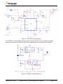
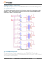
all the possible SPI devices on the board. Figure 3 shows the schematic connections for the SPI
configuration selections. Refer to Section 2.4.3 “Jumper Table” for more details on the jumper
selection options.
The three signals decoded by the 74HC138 to generate the SPI chip-select signals can be driven by
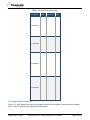
GPIO signals from the Primary Elevator Connector (GPIO7-9) or they can be set by jumper options J14J16. Table 1 shows how the logic level on the three decoder inputs map to the SPI chip-select signals.
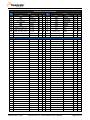
Table 2 shows the devices to which the decoded chip-selects are connected.
TWRADCDACLTCUM
TWR-ADCDAC-LTC Tower Module User's Manual
Page 8 of 17