1
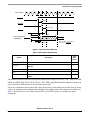
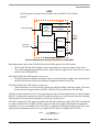
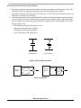
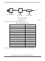
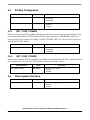
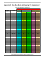
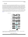
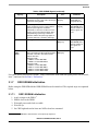
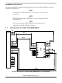
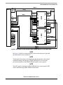
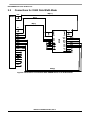
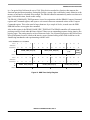
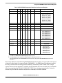
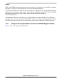
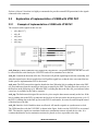
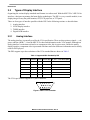
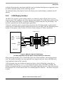
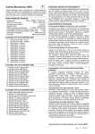
PSC Clock Structure Table 7. RCS Baud Rate Calculation Receive Clock Select Baud Rate 0000–1101 ips_clk / (16 CT[0:15]) 1111 ips_clk / (10 CT[0:15]) 1110 psc_mclk_in / 10 NOTE Transmit clock and receive clock are independent of each other. CSR, CTUR and CTLR registers are in the PSC module (refer to the MPC5121e reference manual). 4.2 PSC in Codec Mode PSC in codec mode uses PSC_MCLK_OUT. A brief introduction to PSC_MCLK_OUT is given below. MCLK_SRC MCLK_EN XCLK MCLK_DIV_OUT REF_CLK PSC_MCLK_IN Power Gate mclk_div SPDIF_RXCLK SPDIF_TXCLK PSC_MCLK_OUT MCLK_1_SRC MCLK_0_SRC Figure 4. Generation of PSC_MCLK_OUT 4.3 Introduction The PSC_MCLK_OUT can be generated from five clock sources. The generation of the clocks is divided into two stages. 1. First is the divider stage, where one of four clock sources is selected by the MCLK_0_SRC field in PnCCR. Then this clock is further divided by the divider, if that clock is enabled by MCLK_EN. If MCLK_EN has been cleared, then the clock is disabled and the input clock source will not reach the divider. 2. In the second stage either the divided clock source or spdif_rxclk can be selected as the final PSC_MCLK_OUT, depending on the value of MCLK_1_SRC. SPDIF_RXCLK bypasses the divider. SPDIF_TXCLK and PSC_MCLK_IN are external clocks and SPDIF_RXCLK is generated by the SPDIF module. External clocks should be provided if these are used as clock sources for generation of PSC_MCLK_OUT. External clock sources can be provided from the appropriate pads. Pin muxing for the pads should be done so that these clocks can reach internally into the chip. See appendix A for pin muxing details about SPDIF_TXCLK and PSC_MCLK_IN, and example code for pin muxing. MPC5121e Clocks, Rev. 0 Freescale Semiconductor 11