1
DRAM Controller Initialization
NOTE
In 16-bit mode (16BITMODE is set) the DDR SDRAM with column
addresses 0 to 7 are not supported, because column address line 7 will be
mapped to internal address line 8 and the row address line 0 cannot be
mapped to internal address line 9.
NOTE
In 16-bit mode (16BITMODE is set) the DRAM controller supports a burst
of eight bytes, and in 32-bit mode (16BITMODE is cleared) a burst size of
four bytes is supported. This has to be configured in the DDR SDRAM
during initialization.
NOTE
There is a correlation between setting the 16BITMODE bit in the DRAM
controller and the I/O configuration. Please refer to Section 5.2,
“MPC5121e DDR SDRAM I/O Configuration,” for more information.
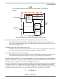
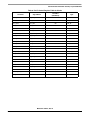
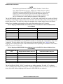
The bit field DRAM_BANK_SELECT controls the bank address mapping. The table 14-5 in chapter
14.2.2.1 “DDR System Configuration Register” in MPC5121ERM, MPC5121e Reference Manual Rev. 3
shows all possible address mappings from internal to DDR SDRAM bank addresses.
NOTE
There must be a seamless transition of the internal addresses when mapping
the bank, column, and row addresses to the internal addresses.
For example, the DDR1 SDRAM, 256 MB with a memory organization of 16 MB X 16, shall be used. The
selected DDR1 DDR has thirteen row address lines (0 to 12), nine column address lines (0 to 8), and two
bank address lines (0 to 1). The DRAM controller shall be used in 32-bit mode.
In 32-bit mode the 16BITMODE bit must be cleared.
The column address line 0 in 32-bit mode is managed internally. Column address lines 1 to 8 will be
mapped to internal address lines 3 to 10.
Because there must be a seamless transition in using the internal address lines, row address line 0 must be
mapped to internal address line 11. This is done by setting the DRAM_ROW_SELECT to 1 (see table 14-7
in chapter 14.2.2.1 “DDR System Configuration Register” in MPC5121ERM, MPC5121e Reference
Manual Rev. 3).
For the selected DDR1 SDRAM only thirteen row address lines are required. This means that bank address
line 0 must be mapped to internal address 24. Because the selected DDR1 SDRAM has only two bank
address lines (four banks), the DRAM_BANK_SELECT must be set to nine (see table 14-5 in chapter
14.2.2.1 “DDR System Configuration Register” in MPC5121ERM, MPC5121e Reference Manual Rev. 3).
5.4.2
Read and Write Latencies
The RDLY bits along with HALF_DQS and QUART_DQS_DLY have to correlate with the read CAS
(column address select) delay setting of the memory. The memory is told what the CAS setting is during
MPC5121e DRAM Controller, Rev. 2
Freescale Semiconductor
69