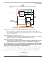
1
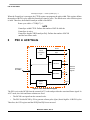
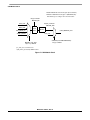
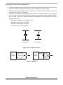
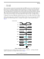
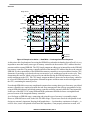
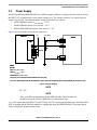
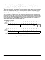
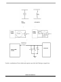
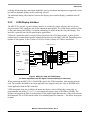
PSC in SPI Mode
6
PSC in SPI Mode
In SPI master mode:
• The BCLK (SCLK) frequency is generated by dividing down the MCLK frequency.
• The DSCLK defines the delay between the SS going active and the first BCLK (SCK) clock pulse
transition. The DSCLK delay is created by dividing down the MCLK frequency. The delay
between consecutive transfers is created by dividing down the IPS_CLK clock frequency.
• DTL stands for length of delay after transfer. The counter/timer determines the length of time the
PSC delays after each serial transfer (the length of time that SS stays high/inactive between
consecutive transfers).
Delay after transfer can be used to ensure that the deselect time requirement is met (for peripherals that
have such a requirement). Some peripherals must be deselected for a minimum period of time between
consecutive serial transfers.
CCR[0:7] + 1
DSCKL Delay = --------------------------------MCLK
CT[0:15] + 2
3
DTL = -------------------------------------------------- + -----------------------------------------IPS_CLK Frequency MCLKFrequency
where CT[0:7] = CTUR[0:7]
CT[8:15] = CTLR[0:7]
7
CAN Module Clock
The CAN_SOURCE_CLK can be generated from five clock sources. The generation of the clocks is
divided into two stages.
1. The first stage is the divider stage, where one of four clock sources is selected by the
MSCAN_CLK_SRC field from the MnCCR register. Then this clock is further divided by the
divider, as long as that clock is enabled by MSCAN_EN. If the clock is disabled by clearing
MSCAN_EN then the input clock source will not reach the divider.
2. In the second stage either the divided clock source or IPS_CLK can be selected as the final
CAN_SOURCE_CLOCK based on the CLKSRC bit in the CANCTL1 register in the MSCAN
module. IPS_CLK bypasses the divider.
SPDIF_TXCLK and PSC_MCLK_IN are external clocks. External clocks should be provided if these are
used as clock sources for the generation of PSC_MCLK_OUT. External clock sources can be provided
from the appropriate pads. Pin muxing for the pads should be done so that these clocks can reach internally
into the chip. Refer to Section 4, “PSC Clock Structure,” for example code for pin muxing
PSC_MCLK_IN and SPDIF_CLK.
NOTE
The MnCCR register is in the clock module while the CANCTL1 register is
in the MSCAN module.
MPC5121e Clocks, Rev. 0
Freescale Semiconductor
15