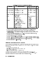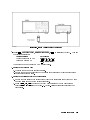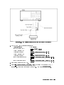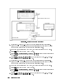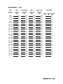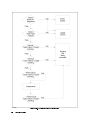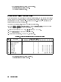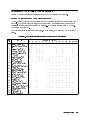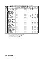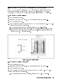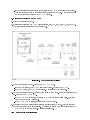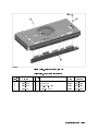
1
Agilent 4395A Network/Spectrum/Impedance Analyzer Service Manual
Manual Change
Agilent Part No. N/A
Oct 2009
Change 1
Add TAR in Frequency Accuracy Test to the following.
Without Option 1D5
Frequency
Minimum
Limit
100 MHz
-550Hz
Test Result
Maximum
Limit
Measurement
Uncertainty
550Hz
± 2.47 Hz
Maximum
Limit
Measurement
Uncertainty
13Hz
± 2.0 Hz
TAR
223
With Option 1D5
Frequency
Minimum
Limit
100 MHz
-13Hz
Test Result
TAR
6.4
Change 2
Add TAR in Source Level Accuracy / Flatness Test to the following.
Level Accuracy
Minimum
Limit
Test
Result
- 1.0 dB
Maximum
Limit
Measurement
Uncertainty
TAR
1.0 dB
± 0.12 dB
Test Result
Maximum
Limit
Measurement
Uncertainty
2.0
2.0
2.0
2.0
2.0
2.0
2.0
2.0
2.0
2.0
2.0
2.0
2.0
2.0
2.0
2.0
± 0.12 dB
± 0.12 dB
± 0.12 dB
± 0.12 dB
± 0.12 dB
± 0.12 dB
± 0.12 dB
± 0.13 dB
± 0.19 dB
± 0.19 dB
± 0.19 dB
± 0.20 dB
± 0.19 dB
± 0.19 dB
± 0.19 dB
± 0.19 dB
9.42
Level Flatness
Frequency
Minimum
Limit
10 Hz
50 Hz
500 Hz
2 kHz
12 kHz
60 kHz
160 kHz
500 kHz
1 MHz
3 MHz
10 MHz
45 MHz
75 MHz
110 MHz
140 MHz
190 MHz
- 2.0
- 2.0
- 2.0
- 2.0
- 2.0
- 2.0
- 2.0
- 2.0
- 2.0
- 2.0
- 2.0
- 2.0
- 2.0
- 2.0
- 2.0
- 2.0
dB
dB
dB
dB
dB
dB
dB
dB
dB
dB
dB
dB
dB
dB
dB
dB
C Copyright 2009 Agilent Technologies
○
dB
dB
dB
dB
dB
dB
dB
dB
dB
dB
dB
dB
dB
dB
dB
dB
TAR
21.01
21.02
21.03
21.01
21.03
21.03
20.86
19.4
13.27
13.27
13.27
13.26
13.27
13.28
13.28
13.28
235 MHz
290 MHz
345 MHz
400 MHz
445 MHz
470 MHz
500 MHz
- 2.0
- 2.0
- 2.0
- 2.0
- 2.0
- 2.0
- 2.0
dB
dB
dB
dB
dB
dB
dB
2.0
2.0
2.0
2.0
2.0
2.0
2.0
dB
dB
dB
dB
dB
dB
dB
± 0.38 dB
± 0.38 dB
± 0.38 dB
± 0.38 dB
± 0.38 dB
± 0.38 dB
± 0.38 dB
6.35
6.35
6.35
6.35
6.35
6.35
6.35
Change 3
Add TAR in Non Sweep Power Linearity Test to the following.
Power
Setting
Minimum
Limit
15 dBm
10 dBm
-10 dBm
-20 dBm
-30 dBm
-40 dBm
-50 dBm
- 1.0 dB
- 1.0 dB
- 1.0 dB
- 1.0 dB
- 1.0 dB
- 1.0 dB
- 1.5 dB
Test Result
Maximum
Limit
Measurement
Uncertainty
1.0 dB
1.0 dB
1.0 dB
1.0 dB
1.0 dB
1.0 dB
1.5 dB
± 0.17 dB
± 0.17dB
± 0.17 dB
± 0.17 dB
± 0.18 dB
± 0.18 dB
± 0.19 dB
TAR
6.58
6.59
6.58
6.35
6.17
6.16
8.99
Change 4
Add TAR in Power Sweep Linearity Test to the following.
STOP
Power
-30 dBm
15 dBm
Source
Power
Minimum
Limit
-35 dBm
-40 dBm
-45 dBm
-50 dBm
10 dBm
5 dBm
0 dBm
-5 dBm
- 0.5 dB
- 0.5 dB
- 0.5 dB
- 0.5 dB
- 0.5 dB
- 0.5 dB
- 0.5 dB
- 0.5 dB
Test
Result
Maximum
Limit
Measurement
Uncertainty
0.5 dB
0.5 dB
0.5 dB
0.5 dB
0.5 dB
0.5 dB
0.5 dB
0.5 dB
± 0.072 dB
± 0.073 dB
± 0.078dB
± 0.15 dB
± 0.059 dB
± 0.059 dB
± 0.061 dB
± 0.066 dB
TAR
7.34
7.23
6.77
3.57
8.96
8.95
8.67
7.92
Change 5
Modify Measurement Uncertainty in HARMONICS/NON-HARMONIC SPURIOUS TEST
Harmonics
Frequency
Harmonics
Frequency
10 kHz
20 kHz
30 kHz
1 MHz
1.5 MHz
20 MHz
30 MHz
200 MHz
300 MHz
500 MHz
750 MHz
500 kHz
10 MHz
100 MHz
250 MHz
Test Result
C Copyright 2009 Agilent Technologies
○
Test Limit
Measurement
Uncertainty
< -30 dBc
< -30 dBc
< -30 dBc
< -30 dBc
< -30 dBc
< -30 dBc
< -30 dBc
< -30 dBc
< -30 dBc
< -30 dBc
± 0.93 dB
± 0.98 dB
± 0.91 dB
± 0.88 dB
± 1.02 dB
± 0.87 dB
± 1.01 dB
± 1.01 dB
± 1.62 dB
± 1.62 dB
500 MHz
1 GHz
1.5 GHz
< -30 dBc
< -30 dBc
± 1.62 dB
± 1.63 dB
Test Limit
Measurement
Uncertainty
< -30 dBc
< -30 dBc
< -30 dBc
< -30 dBc
< -30 dBc
± 1.52 dB
± 2.10 dB
± 1.72 dB
± 1.70 dB
± 1.63 dB
Non-Harmonic Spurious
Frequency
Harmonics
Frequency
10 kHz
230 MHz
330 MHz
430 MHz
500 MHz
830.00001 MHz
600 MHz
500 MHz
400 MHz
330 MHz
Test Result
Change 6
Add TAR in DC Bias Accuracy Test to the following.
Dc Bias
DCV
Test Result
-40 V
-10 V
-4 V
0V
4V
10 V
40 V
Test Limit
< ± 44 mV
< ± 14 mV
< ± 8 mV
< ± 4 mV
< ± 8 mV
< ± 14 mV
< ± 44 mV
< ± 0.530
mA
< ± 0.080
mA
< ± 0.035
mA
< ± 0.030
mA
< ± 0.030
mA
< ± 0.035
mA
< ± 0.080
mA
< ± 0.530
mA
-100 mA
-10 mA
-1 mA
-20 uA
DCI
20 uA
1 mA
10 mA
100 mA
Measurement
Uncertainty
± 0.858 mV
± 0.38 mV
± 0.0613 mV
± 0.0354 mV
± 0.0613 mV
± 0.380 mV
± 0.858 mV
TAR
51.3
36.8
130.5
113
130.5
36.8
51.3
± 0.17 mA
32.2
± 0.77 uA
104.5
± 0.40 uA
87.9
± 0.49 uA
61.9
± 0.49 uA
61.9
± 0.40 uA
87.9
± 0.77 uA
104.5
± 0.17 mA
32.2
Change 7
Add TAR in Absolute Amplitude Accuracy Test to the following.
Input R
Frequency
Minimum
Limit
100 Hz
200 Hz
500 Hz
1 kHz
2 kHz
- 1.5 dB
- 1.5 dB
- 1.5 dB
- 1.5 dB
- 1.5 dB
Test Result
Maximum
Limit
Measurement
Uncertainty
1.5 dB
1.5 dB
1.5 dB
1.5 dB
1.5 dB
± 0.19 dB
± 0.19 dB
± 0.19 dB
± 0.19 dB
± 0.19 dB
C Copyright 2009 Agilent Technologies
○
TAR
9.21
9.23
9.23
9.24
9.25
5 kHz
10 kHz
20 kHz
50 kHz
100 kHz
200 kHz
500 kHz
1 MHz
2 MHz
5 MHz
8 MHz
10 MHz
20 MHz
50 MHz
100 MHz
125 MHz
175 MHz
200 MHz
225 MHz
275 MHz
300 MHz
325 MHz
375 MHz
400 MHz
425 MHz
475 MHz
500 MHz
- 1.5 dB
- 1.5 dB
- 1.5 dB
- 1.5 dB
- 1.5 dB
- 1.5 dB
- 1.5 dB
- 1.5 dB
- 1.5 dB
- 1.5 dB
- 1.5 dB
- 1.5 dB
- 1.5 dB
- 1.5 dB
- 1.5 dB
- 1.5 dB
- 1.5 dB
- 1.5 dB
- 1.5 dB
- 1.5 dB
- 1.5 dB
- 1.5 dB
- 1.5 dB
- 1.5 dB
- 1.5 dB
- 1.5 dB
- 1.5 dB
1.5 dB
1.5 dB
1.5 dB
1.5 dB
1.5 dB
1.5 dB
1.5 dB
1.5 dB
1.5 dB
1.5 dB
1.5 dB
1.5 dB
1.5 dB
1.5 dB
1.5 dB
1.5 dB
1.5 dB
1.5 dB
1.5 dB
1.5 dB
1.5 dB
1.5 dB
1.5 dB
1.5 dB
1.5 dB
1.5 dB
1.5 dB
± 0.19 dB
± 0.19 dB
± 0.19 dB
± 0.19 dB
± 0.17 dB
± 0.17 dB
± 0.18 dB
± 0.21 dB
± 0.21 dB
± 0.22 dB
± 0.22 dB
± 0.22 dB
± 0.21 dB
± 0.21 dB
± 0.22 dB
± 0.24 dB
± 0.24 dB
± 0.24 dB
± 0.23 dB
± 0.24 dB
± 0.24 dB
± 0.24 dB
± 0.24 dB
± 0.24 dB
± 0.24 dB
± 0.24 dB
± 0.27 dB
Maximum
Limit
Measurement
Uncertainty
1.5 dB
1.5 dB
1.5 dB
1.5 dB
1.5 dB
1.5 dB
1.5 dB
1.5 dB
1.5 dB
1.5 dB
1.5 dB
1.5 dB
1.5 dB
1.5 dB
1.5 dB
1.5 dB
1.5 dB
1.5 dB
± 0.19 dB
± 0.19 dB
± 0.19 dB
± 0.19 dB
± 0.19 dB
± 0.19 dB
± 0.19 dB
± 0.19 dB
± 0.19 dB
± 0.17 dB
± 0.17 dB
± 0.18 dB
± 0.21 dB
± 0.21 dB
± 0.22 dB
± 0.22 dB
± 0.22 dB
± 0.21 dB
9.24
9.22
9.21
9.10
10.04
10.04
9.56
8.14
8.13
8.11
8.12
8.12
8.14
8.13
8.11
7.33
7.38
7.39
7.42
7.35
7.34
7.39
7.35
7.33
7.29
7.28
6.34
Input A
Frequency
Minimum
Limit
100 Hz
200 Hz
500 Hz
1 kHz
2 kHz
5 kHz
10 kHz
20 kHz
50 kHz
100 kHz
200 kHz
500 kHz
1 MHz
2 MHz
5 MHz
8 MHz
10 MHz
20 MHz
- 1.5 dB
- 1.5 dB
- 1.5 dB
- 1.5 dB
- 1.5 dB
- 1.5 dB
- 1.5 dB
- 1.5 dB
- 1.5 dB
- 1.5 dB
- 1.5 dB
- 1.5 dB
- 1.5 dB
- 1.5 dB
- 1.5 dB
- 1.5 dB
- 1.5 dB
- 1.5 dB
Test Result
C Copyright 2009 Agilent Technologies
○
TAR
9.21
9.23
9.23
9.24
9.25
9.24
9.22
9.21
9.10
10.04
10.04
9.56
8.14
8.13
8.11
8.12
8.12
8.14
50 MHz
100 MHz
125 MHz
175 MHz
200 MHz
225 MHz
275 MHz
300 MHz
325 MHz
375 MHz
400 MHz
425 MHz
475 MHz
500 MHz
- 1.5 dB
- 1.5 dB
- 1.5 dB
- 1.5 dB
- 1.5 dB
- 1.5 dB
- 1.5 dB
- 1.5 dB
- 1.5 dB
- 1.5 dB
- 1.5 dB
- 1.5 dB
- 1.5 dB
- 1.5 dB
1.5 dB
1.5 dB
1.5 dB
1.5 dB
1.5 dB
1.5 dB
1.5 dB
1.5 dB
1.5 dB
1.5 dB
1.5 dB
1.5 dB
1.5 dB
1.5 dB
± 0.21 dB
± 0.22 dB
± 0.24 dB
± 0.24 dB
± 0.24 dB
± 0.23 dB
± 0.24 dB
± 0.24 dB
± 0.24 dB
± 0.24 dB
± 0.24 dB
± 0.24 dB
± 0.24 dB
± 0.27 dB
Maximum
Limit
Measurement
Uncertainty
1.5 dB
1.5 dB
1.5 dB
1.5 dB
1.5 dB
1.5 dB
1.5 dB
1.5 dB
1.5 dB
1.5 dB
1.5 dB
1.5 dB
1.5 dB
1.5 dB
1.5 dB
1.5 dB
1.5 dB
1.5 dB
1.5 dB
1.5 dB
1.5 dB
1.5 dB
1.5 dB
1.5 dB
1.5 dB
1.5 dB
1.5 dB
1.5 dB
1.5 dB
1.5 dB
1.5 dB
± 0.19 dB
± 0.19 dB
± 0.19 dB
± 0.19 dB
± 0.19 dB
± 0.19 dB
± 0.19 dB
± 0.19 dB
± 0.19 dB
± 0.17 dB
± 0.17 dB
± 0.18 dB
± 0.21 dB
± 0.21 dB
± 0.22 dB
± 0.22 dB
± 0.22 dB
± 0.21 dB
± 0.21 dB
± 0.22 dB
± 0.24 dB
± 0.24 dB
± 0.24 dB
± 0.23 dB
± 0.24 dB
± 0.24 dB
± 0.24 dB
± 0.24 dB
± 0.24 dB
± 0.24 dB
± 0.24 dB
8.13
8.11
7.33
7.38
7.39
7.42
7.35
7.34
7.39
7.35
7.33
7.29
7.28
6.34
Input B
Frequency
Minimum
Limit
100 Hz
200 Hz
500 Hz
1 kHz
2 kHz
5 kHz
10 kHz
20 kHz
50 kHz
100 kHz
200 kHz
500 kHz
1 MHz
2 MHz
5 MHz
8 MHz
10 MHz
20 MHz
50 MHz
100 MHz
125 MHz
175 MHz
200 MHz
225 MHz
275 MHz
300 MHz
325 MHz
375 MHz
400 MHz
425 MHz
475 MHz
- 1.5 dB
- 1.5 dB
- 1.5 dB
- 1.5 dB
- 1.5 dB
- 1.5 dB
- 1.5 dB
- 1.5 dB
- 1.5 dB
- 1.5 dB
- 1.5 dB
- 1.5 dB
- 1.5 dB
- 1.5 dB
- 1.5 dB
- 1.5 dB
- 1.5 dB
- 1.5 dB
- 1.5 dB
- 1.5 dB
- 1.5 dB
- 1.5 dB
- 1.5 dB
- 1.5 dB
- 1.5 dB
- 1.5 dB
- 1.5 dB
- 1.5 dB
- 1.5 dB
- 1.5 dB
- 1.5 dB
Test Result
C Copyright 2009 Agilent Technologies
○
TAR
9.21
9.23
9.23
9.24
9.25
9.24
9.22
9.21
9.10
10.04
10.04
9.56
8.14
8.13
8.11
8.12
8.12
8.14
8.13
8.11
7.33
7.38
7.39
7.42
7.35
7.34
7.39
7.35
7.33
7.29
7.28
500 MHz
- 1.5 dB
1.5 dB
± 0.27 dB
6.34
Change 8
Add TAR in Magnitude Ratio / Phase Dynamic Accuracy Test to the following.
A/R Measurement
Input
Level
*
Measurement
0 dB
Magnitude
Ratio
Phase
Input
Level
*
-20
dB
-30
dB
-40
dB
-50
dB
-60
dB
-70
dB
-80
dB
-90
dB
-100
dB
Measurement
Magnitude
Ratio
Phase
Magnitude
Ratio
Phase
Magnitude
Ratio
Phase
Magnitude
Ratio
Phase
Magnitude
Ratio
Phase
Magnitude
Ratio
Phase
Magnitude
Ratio
Phase
Magnitude
Ratio
Phase
Magnitude
Ratio
Phase
Minimum
Limit
Test Result
Maximum
Limit
Measurement
Uncertainty
TAR
- 0.40 dB
0.40 dB
± 0.011 dB
38.75
- 3.0 deg
3.0 deg
± 0.068 deg
44.40
Minimum
Limit
Test Result
Maximum
Limit
Measurement
Uncertainty
TAR
- 0.05 dB
0.05 dB
± 0.0092 dB
5.45
- 0.3 deg
0.3 deg
± 0.064 deg
4.66
- 0.05 dB
0.05 dB
± 0.0093 dB
5.42
- 0.3 deg
0.3 deg
± 0.064 deg
4.69
- 0.05 dB
0.05 dB
± 0.0096 dB
5.23
- 0.3 deg
0.3 deg
± 0.064 deg
4.70
- 0.05 dB
0.05 dB
± 0.011 dB
4.39
- 0.3 deg
0.3 deg
± 0.065 deg
4.64
- 0.05 dB
0.05 dB
± 0.013 dB
3.78
- 0.3 deg
0.3 deg
± 0.076 deg
3.94
- 0.3 dB
0.3 dB
± 0.027 dB
11.59
- 1.8 deg
1.8 deg
± 0.15 deg
12.13
- 0.3 dB
0.3 dB
± 0.071 dB
4.34
- 1.8 deg
1.8 deg
± 0.43 deg
4.15
- 3.0 dB
3.0 dB
± 0.24 dB
17.58
- 18 deg
18 deg
± 1.6 deg
11.59
- 3.00 dB
3.00 dB
± 0.71 dB
5.61
- 18 deg
18 deg
± 5.3deg
3.39
B/R Measurement
Input
Level
*
Measurement
0 dB
Magnitude
Ratio
Phase
Minimum
Limit
Test Result
Maximum
Limit
Measurement
Uncertainty
TAR
- 0.40 dB
0.40 dB
± 0.011 dB
38.75
- 3.0 deg
3.0 deg
± 0.068 deg
44.40
C Copyright 2009 Agilent Technologies
○
Input
Level
*
-20
dB
-30
dB
-40
dB
-50
dB
-60
dB
-70
dB
-80
dB
-90
dB
-100
dB
Measurement
Magnitude
Ratio
Phase
Magnitude
Ratio
Phase
Magnitude
Ratio
Phase
Magnitude
Ratio
Phase
Magnitude
Ratio
Phase
Magnitude
Ratio
Phase
Magnitude
Ratio
Phase
Magnitude
Ratio
Phase
Magnitude
Ratio
Phase
Minimum
Limit
Test Result
Maximum
Limit
Measurement
Uncertainty
- 0.05 dB
0.05 dB
± 0.0092 dB
5.45
- 0.3 deg
0.3 deg
± 0.064 deg
4.66
- 0.05 dB
0.05 dB
± 0.0093 dB
5.42
- 0.3 deg
0.3 deg
± 0.064 deg
4.69
- 0.05 dB
0.05 dB
± 0.0096 dB
5.23
- 0.3 deg
0.3 deg
± 0.064 deg
4.70
- 0.05 dB
0.05 dB
± 0.011 dB
4.39
- 0.3 deg
0.3 deg
± 0.065 deg
4.64
- 0.05 dB
0.05 dB
± 0.013 dB
3.78
- 0.3 deg
0.3 deg
± 0.076 deg
3.94
- 0.3 dB
0.3 dB
± 0.027 dB
11.59
- 1.8 deg
1.8 deg
± 0.15 deg
12.13
- 0.3 dB
0.3 dB
± 0.071 dB
4.34
- 1.8 deg
1.8 deg
± 0.43 deg
4.15
- 3.0 dB
3.0 dB
± 0.24 dB
17.58
- 18 deg
18 deg
± 1.6 deg
11.59
- 3.00 dB
3.00 dB
± 0.71 dB
5.61
- 18 deg
18 deg
± 5.3 deg
3.39
Change 9
Add TAR in Amplitude Fidelity Test to the following.
Input R
dB from
Reference
Input
Level
Minimum
Limit
10 dB
-10 dB
-20 dB
-30 dB
-40 dB
-50 dB
-60 dB
-70 dB
- 0.05 dB
- 0.05 dB
- 0.05 dB
- 0.07 dB
- 0.15 dB
- 0.35 dB
- 0.8 dB
- 1.8 dB
Test Result
Maximum
Limit
0.05 dB
0.05 dB
0.05 dB
0.07 dB
0.15 dB
0.35 dB
0.8 dB
1.8 dB
Measurement
Uncertainty
± 0.016 dB
± 0.015 dB
± 0.015 dB
± 0.015 dB
± 0.018 dB
± 0.026 dB
± 0.084 dB
± 0.227 dB
TAR
3.14
3.31
3.33
4.60
8.57
13.99
10.39
9.57
Input A
dB from
Reference
Input
Minimum
Limit
TAR
Test Result
Maximum
Limit
C Copyright 2009 Agilent Technologies
○
Measurement
Uncertainty
TAR
Level
10 dB
-10 dB
-20 dB
-30 dB
-40 dB
-50 dB
-60 dB
-70 dB
- 0.05 dB
- 0.05 dB
- 0.05 dB
- 0.07 dB
- 0.15 dB
- 0.35 dB
- 0.8 dB
- 1.8 dB
0.05 dB
0.05 dB
0.05 dB
0.07 dB
0.15 dB
0.35 dB
0.8 dB
1.8 dB
dB from
Reference
Input
Level
Minimum
Limit
Maximum
Limit
10 dB
-10 dB
-20 dB
-30 dB
-40 dB
-50 dB
-60 dB
-70 dB
- 0.05 dB
- 0.05 dB
- 0.05 dB
- 0.07 dB
- 0.15 dB
- 0.35 dB
- 0.8 dB
- 1.8 dB
± 0.016 dB
± 0.015 dB
± 0.015 dB
± 0.015 dB
± 0.018 dB
± 0.026 dB
± 0.084 dB
± 0.227 dB
3.14
3.31
3.33
4.60
8.57
13.99
10.39
9.57
Input B
Test Result
0.05 dB
0.05 dB
0.05 dB
0.07 dB
0.15 dB
0.35 dB
0.8 dB
1.8 dB
Measurement
Uncertainty
TAR
± 0.016 dB
± 0.015 dB
± 0.015 dB
± 0.015 dB
± 0.018 dB
± 0.026 dB
± 0.084 dB
± 0.227 dB
3.14
3.31
3.33
4.60
8.57
13.99
10.39
9.57
Change 10
Add TAR in Input Attenuator Switching Uncertainty Test to the following.
Input R
Input
Minimum
Attenuation Limit
0 dB
20 dB
30 dB
40 dB
50 dB
Test
Result
- 1 dB
- 1 dB
- 1 dB
- 1.5 dB
- 1.5 dB
Maximum
Limit
Measurement
Uncertainty
1 dB
1 dB
1 dB
1.5 dB
1.5 dB
± 0.025 dB
± 0.024 dB
± 0.024 dB
± 0.027 dB
± 0.084 dB
Maximum
Limit
Measurement
Uncertainty
1 dB
1 dB
1 dB
1.5 dB
1.5 dB
± 0.025 dB
± 0.024 dB
± 0.024 dB
± 0.027 dB
± 0.084 dB
TAR
45.16
47.30
46.78
66.76
21.20
Input A
Input
Minimum
Attenuation Limit
0 dB
20 dB
30 dB
40 dB
50 dB
- 1 dB
- 1 dB
- 1 dB
- 1.5 dB
- 1.5 dB
Test
Result
Input B
C Copyright 2009 Agilent Technologies
○
TAR
45.16
47.30
46.78
66.76
21.20
Input
Minimum
Attenuation Limit
0 dB
20 dB
30 dB
40 dB
50 dB
Test
Result
- 1 dB
- 1 dB
- 1 dB
- 1.5 dB
- 1.5 dB
Maximum
Limit
Measurement
Uncertainty
1 dB
1 dB
1 dB
1.5 dB
1.5 dB
± 0.025 dB
± 0.024 dB
± 0.024 dB
± 0.027 dB
± 0.084 dB
TAR
45.16
47.30
46.78
66.76
21.20
Change 11
Modify Measurement Uncertainty in NOISE SIDEBANDS TEST
INPUT R
Frequency
Offset
from Carrier
10 MHz
-1 kHz
+1 kHz
-10 kHz
+10 kHz
-100 kHz
+100 kHz
-1 MHz
+1 MHz
-1 kHz
+1 kHz
-10 kHz
+10 kHz
-100 kHz
+100 kHz
-1 MHz
+1 MHz
-1 kHz
+1 kHz
-10 kHz
+10 kHz
-100 kHz
+100 kHz
-1 MHz
+1 MHz
100 MHz
500 MHz
Test
Result
Test Limit
Measurement
Uncertainty
< -97 dBc/Hz
< -97 dBc/Hz
< -97 dBc/Hz
< -97 dBc/Hz
< -110 dBc/Hz
< -110 dBc/Hz
< -110 dBc/Hz
< -110 dBc/Hz
< -97 dBc/Hz
< -97 dBc/Hz
< -97 dBc/Hz
< -97 dBc/Hz
< -110 dBc/Hz
< -110 dBc/Hz
< -110 dBc/Hz
< -110 dBc/Hz
< -97 dBc/Hz
< -97 dBc/Hz
< -97 dBc/Hz
< -97 dBc/Hz
< -110 dBc/Hz
< -110 dBc/Hz
< -110 dBc/Hz
< -110 dBc/Hz
± 0.026 dB
± 0.026 dB
± 0.012 dB
± 0.012 dB
± 0.025 dB
± 0.025 dB
± 0.015 dB
± 0.015 dB
± 0.025 dB
± 0.025 dB
± 0.012 dB
± 0.012 dB
± 0.026 dB
± 0.026 dB
± 0.014 dB
± 0.014 dB
± 0.025 dB
± 0.025 dB
± 0.012 dB
± 0.012 dB
± 0.026 dB
± 0.026 dB
± 0.016 dB
± 0.016 dB
Change 12
Add TAR in Amplitude Accuracy/Frequency Response Test to the following.
Input R
Level Accuracy
Minimum
Limit
Test
Result
- 0.8 dB
Maximum
Limit
Measurement
0.8 dB
± 0.14 dB
Frequency Response
C Copyright 2009 Agilent Technologies
○
TAR
6.19
Frequency
Minimum
Limit
10 Hz
15 Hz
25 Hz
40 Hz
80 Hz
100 Hz
200 Hz
500 Hz
1 kHz
2 kHz
5 kHz
10 kHz
20 kHz
50 kHz
100 kHz
200 kHz
500 kHz
1 MHz
2 MHz
5 MHz
8 MHz
10 MHz
20 MHz
100 MHz
125 MHz
150 MHz
175 MHz
200 MHz
225 MHz
250 MHz
275 MHz
300 MHz
325 MHz
350 MHz
375 MHz
400 MHz
425 MHz
450 MHz
475 MHz
500 MHz
- 3.0 dB
- 3.0 dB
- 3.0 dB
- 3.0 dB
- 3.0 dB
- 1.3 dB
- 1.3 dB
- 1.3 dB
- 1.3 dB
- 1.3 dB
- 1.3 dB
- 1.3 dB
- 1.3 dB
- 1.3 dB
- 1.3 dB
- 1.3 dB
- 1.3 dB
- 1.3 dB
- 1.3 dB
- 1.3 dB
- 1.3 dB
- 1.3 dB
- 1.3 dB
- 1.3 dB
- 1.3 dB
- 1.3 dB
- 1.3 dB
- 1.3 dB
- 1.3 dB
- 1.3 dB
- 1.3 dB
- 1.3 dB
- 1.3 dB
- 1.3 dB
- 1.3 dB
- 1.3 dB
- 1.3 dB
- 1.3 dB
- 1.3 dB
- 1.3 dB
Test Result
Maximum
Limit
Measurement
Uncertainty
3.0 dB
3.0 dB
3.0 dB
3.0 dB
3.0 dB
1.3 dB
1.3 dB
1.3 dB
1.3 dB
1.3 dB
1.3 dB
1.3 dB
1.3 dB
1.3 dB
1.3 dB
1.3 dB
1.3 dB
1.3 dB
1.3 dB
1.3 dB
1.3 dB
1.3 dB
1.3 dB
1.3 dB
1.3 dB
1.3 dB
1.3 dB
1.3 dB
1.3 dB
1.3 dB
1.3 dB
1.3 dB
1.3 dB
1.3 dB
1.3 dB
1.3 dB
1.3 dB
1.3 dB
1.3 dB
1.3 dB
± 0.29 dB
± 0.29 dB
± 0.29 dB
± 0.29 dB
± 0.30 dB
± 0.30 dB
± 0.30 dB
± 0.30 dB
± 0.30 dB
± 0.33 dB
± 0.39 dB
± 0.30 dB
± 0.33 dB
± 0.39 dB
± 0.30 dB
± 0.33 dB
± 0.30 dB
± 0.098 dB
± 0.093 dB
± 0.090 dB
± 0.086 dB
± 0.088 dB
± 0.083 dB
± 0.082 dB
± 0.083 dB
± 0.082 dB
± 0.10 dB
± 0.10 dB
± 0.10 dB
± 0.10 dB
± 0.10 dB
± 0.10 dB
± 0.10 dB
± 0.10 dB
± 0.10 dB
± 0.096 dB
± 0.097 dB
± 0.096 dB
± 0.094 dB
± 0.096dB
Input A
Level Accuracy
Minimum
Limit
Test
Result
Maximum
Limit
Measurement
C Copyright 2009 Agilent Technologies
○
TAR
TAR
14.34
14.29
14.22
14.17
14.16
4.96
4.96
4.96
4.96
4.36
3.75
4.96
4.36
3.75
4.96
4.36
4.96
15.25
16.07
16.73
17.54
16.98
18.06
18.23
18.18
18.20
14.84
14.87
14.80
14.71
14.58
14.46
14.38
14.49
14.71
15.69
15.41
15.61
15.93
15.61
- 0.8 dB
0.8 dB
± 0.14 dB
6.19
Frequency Response
Frequency
Minimum
Limit
10 Hz
15 Hz
25 Hz
40 Hz
80 Hz
100 Hz
200 Hz
500 Hz
1 kHz
2 kHz
5 kHz
10 kHz
20 kHz
50 kHz
100 kHz
200 kHz
500 kHz
1 MHz
2 MHz
5 MHz
8 MHz
10 MHz
20 MHz
100 MHz
125 MHz
150 MHz
175 MHz
200 MHz
225 MHz
250 MHz
275 MHz
300 MHz
325 MHz
350 MHz
375 MHz
400 MHz
425 MHz
450 MHz
475 MHz
500 MHz
- 3.0 dB
- 3.0 dB
- 3.0 dB
- 3.0 dB
- 3.0 dB
- 1.3 dB
- 1.3 dB
- 1.3 dB
- 1.3 dB
- 1.3 dB
- 1.3 dB
- 1.3 dB
- 1.3 dB
- 1.3 dB
- 1.3 dB
- 1.3 dB
- 1.3 dB
- 1.3 dB
- 1.3 dB
- 1.3 dB
- 1.3 dB
- 1.3 dB
- 1.3 dB
- 1.3 dB
- 1.3 dB
- 1.3 dB
- 1.3 dB
- 1.3 dB
- 1.3 dB
- 1.3 dB
- 1.3 dB
- 1.3 dB
- 1.3 dB
- 1.3 dB
- 1.3 dB
- 1.3 dB
- 1.3 dB
- 1.3 dB
- 1.3 dB
- 1.3 dB
Test Result
Maximum
Limit
Measurement
Uncertainty
3.0 dB
3.0 dB
3.0 dB
3.0 dB
3.0 dB
1.3 dB
1.3 dB
1.3 dB
1.3 dB
1.3 dB
1.3 dB
1.3 dB
1.3 dB
1.3 dB
1.3 dB
1.3 dB
1.3 dB
1.3 dB
1.3 dB
1.3 dB
1.3 dB
1.3 dB
1.3 dB
1.3 dB
1.3 dB
1.3 dB
1.3 dB
1.3 dB
1.3 dB
1.3 dB
1.3 dB
1.3 dB
1.3 dB
1.3 dB
1.3 dB
1.3 dB
1.3 dB
1.3 dB
1.3 dB
1.3 dB
± 0.29 dB
± 0.29 dB
± 0.29 dB
± 0.29 dB
± 0.30 dB
± 0.30 dB
± 0.30 dB
± 0.30 dB
± 0.30 dB
± 0.33 dB
± 0.39 dB
± 0.30 dB
± 0.33 dB
± 0.39 dB
± 0.30 dB
± 0.33 dB
± 0.30 dB
± 0.098 dB
± 0.093 dB
± 0.090 dB
± 0.086 dB
± 0.088 dB
± 0.083 dB
± 0.082 dB
± 0.083 dB
± 0.082 dB
± 0.10 dB
± 0.10 dB
± 0.10 dB
± 0.10 dB
± 0.10 dB
± 0.10 dB
± 0.10 dB
± 0.10 dB
± 0.10 dB
± 0.096 dB
± 0.097 dB
± 0.096 dB
± 0.094 dB
± 0.096 dB
C Copyright 2009 Agilent Technologies
○
TAR
14.34
14.29
14.22
14.17
14.16
4.96
4.96
4.96
4.96
4.36
3.75
4.96
4.36
3.75
4.96
4.36
4.96
15.25
16.07
16.73
17.54
16.98
18.06
18.23
18.18
18.20
14.84
14.87
14.80
14.71
14.58
14.46
14.38
14.49
14.71
15.69
15.41
15.61
15.93
15.61
Input B
Level Accuracy
Minimum
Limit
Test
Result
- 0.8 dB
Maximum
Limit
Measurement
0.8 dB
± 0.14 dB
TAR
6.19
Frequency Response
Frequency
Minimum
Limit
10 Hz
15 Hz
25 Hz
40 Hz
80 Hz
100 Hz
200 Hz
500 Hz
1 kHz
2 kHz
5 kHz
10 kHz
20 kHz
50 kHz
100 kHz
200 kHz
500 kHz
1 MHz
2 MHz
5 MHz
8 MHz
10 MHz
20 MHz
100 MHz
125 MHz
150 MHz
175 MHz
200 MHz
225 MHz
250 MHz
275 MHz
300 MHz
325 MHz
350 MHz
375 MHz
400 MHz
425 MHz
- 3.0 dB
- 3.0 dB
- 3.0 dB
- 3.0 dB
- 3.0 dB
- 1.3 dB
- 1.3 dB
- 1.3 dB
- 1.3 dB
- 1.3 dB
- 1.3 dB
- 1.3 dB
- 1.3 dB
- 1.3 dB
- 1.3 dB
- 1.3 dB
- 1.3 dB
- 1.3 dB
- 1.3 dB
- 1.3 dB
- 1.3 dB
- 1.3 dB
- 1.3 dB
- 1.3 dB
- 1.3 dB
- 1.3 dB
- 1.3 dB
- 1.3 dB
- 1.3 dB
- 1.3 dB
- 1.3 dB
- 1.3 dB
- 1.3 dB
- 1.3 dB
- 1.3 dB
- 1.3 dB
- 1.3 dB
Test Result
Maximum
Limit
Measurement
Uncertainty
3.0 dB
3.0 dB
3.0 dB
3.0 dB
3.0 dB
1.3 dB
1.3 dB
1.3 dB
1.3 dB
1.3 dB
1.3 dB
1.3 dB
1.3 dB
1.3 dB
1.3 dB
1.3 dB
1.3 dB
1.3 dB
1.3 dB
1.3 dB
1.3 dB
1.3 dB
1.3 dB
1.3 dB
1.3 dB
1.3 dB
1.3 dB
1.3 dB
1.3 dB
1.3 dB
1.3 dB
1.3 dB
1.3 dB
1.3 dB
1.3 dB
1.3 dB
1.3 dB
± 0.29 dB
± 0.29 dB
± 0.29 dB
± 0.29 dB
± 0.30 dB
± 0.30 dB
± 0.30 dB
± 0.30 dB
± 0.30 dB
± 0.33 dB
± 0.39 dB
± 0.30 dB
± 0.33 dB
± 0.39 dB
± 0.30 dB
± 0.33 dB
± 0.30 dB
± 0.098 dB
± 0.093 dB
± 0.090 dB
± 0.086 dB
± 0.088 dB
± 0.083 dB
± 0.082 dB
± 0.083 dB
± 0.082 dB
± 0.10 dB
± 0.10 dB
± 0.10 dB
± 0.10 dB
± 0.10 dB
± 0.10 dB
± 0.10 dB
± 0.10 dB
± 0.10 dB
± 0.096 dB
± 0.097 dB
C Copyright 2009 Agilent Technologies
○
TAR
14.34
14.29
14.22
14.17
14.16
4.96
4.96
4.96
4.96
4.36
3.75
4.96
4.36
3.75
4.96
4.36
4.96
15.25
16.07
16.73
17.54
16.98
18.06
18.23
18.18
18.20
14.84
14.87
14.80
14.71
14.58
14.46
14.38
14.49
14.71
15.69
15.41
450 MHz
475 MHz
500 MHz
- 1.3 dB
- 1.3 dB
- 1.3 dB
1.3 dB
1.3 dB
1.3 dB
C Copyright 2009 Agilent Technologies
○
± 0.096 dB
± 0.094 dB
± 0.096 dB
15.61
15.93
15.61
Agilent 4395A Network/Spectrum/Impedance Analyzer Service Manual
Manual Change
Agilent Part No. N/A
May 2007
Change 1
Change the procedure of the step 2.j (page 2-47 and 2-49) to the following.
j. Press
,
and STATISTICS on OFF. (Then the softkey label changes to STATISTICS ON off.)
Press
, and turn RPG knob until marker is set to sweep STOP frequency point (500 MHz).
Press
, MORE, ELEC DELAY MENU, MKR→DELAY and, ELECTRICAL DELAY.
Then press
or
and turn the RPG knob to vary the electrical delay until the trace is in the most horizontal
position.
C Copyright 2007 Agilent Technologies
○
Agilent 4395A Network/Spectrum/Impedance Analyzer Service Manual
Manual Change
Agilent Part No. N/A
March 2007
Change 1
Change the procedure of the step 3 (page 2-5) to the following.
3. Press
, ANALYZER TYPE, NETWORK ANALYZER,
to initialize the 4395A.
Then set the controls as follows:
Control Settings
Key Strokes
Center Frequency: 50 MHz
,
,
,
Frequency Span: 0 Hz
, ZERO SPAN
Trigger Mode: Single
, SINGLE
The source power now is set to 0 dBm (preset value).
Manually trigger the 4395A each time the Center Frequency setting is changed.
C Copyright 2007 Agilent Technologies
○
Service Manual
Agilent 4395A Network/Spectrum/Impedance Analyzer
SERIAL NUMBERS
This manual applies directly to instruments with serial number
prex JP1KE02197 or above, and MY41100220 or above.
For additional important information about serial
numbers, read \Serial Number" in Appendix A.
Agilent Part No. 04395-90120
Printed in Japan
August 2002
Fifth Edition
Notice
The information contained in this document is subject to change without notice.
This document contains proprietary information that is protected by copyright. All rights are
reserved. No part of this document may be photocopied, reproduced, or translated to another
language without the prior written consent of the Agilent Technologies Company.
Agilent Technologies Japan, LTD.
Kobe Instrument Division
1-3-2, Murotani, Nishi-Ku, Kobe-shi,
Hyogo, 651-2241 Japan
c Copyright 1998, 2000-2002 Agilent Technologies Japan, Ltd.
Manual Printing History
The manual's printing date and part number indicate its current edition. The printing date
changes when a new edition is printed. (Minor corrections and updates that are incorporated
at reprint do not cause the date to change.) The manual part number changes when extensive
technical changes are incorporated.
February 1998 : : : : : : : : : : : : : : : : : : : : : : : : : : : : : : : : : : : First Edition (Part Number 04395-90100)
September 1998 : : : : : : : : : : : : : : : : : : : : : : : : : : : : : : : Second Edition (Part Number 04395-90110)
June 2000 : : : : : : : : : : : : : : : : : : : : : : : : : : : : : : : : : : : : : : Third Edition (Part Number 04395-90110)
March 2001 : : : : : : : : : : : : : : : : : : : : : : : : : : : : : : : : : : : : Fourth Edition (Part Number 04395-90110)
August 2002 : : : : : : : : : : : : : : : : : : : : : : : : : : : : : : : : : : : : : Fifth Edition (Part Number 04395-90120)
iii
Safety Summary
The following general safety precautions must be observed during all phases of operation,
service, and repair of this instrument. Failure to comply with these precautions or with
specic WARNINGS elsewhere in this manual may impair the protection provided by the
equipment. In addition it violates safety standards of design, manufacture, and intended use
of the instrument.
The Agilent Technologies Company assumes no liability for the customer's failure to comply
with these requirements.
Note
4395A comply with INSTALLATION CATEGORY II and POLLUTION
DEGREE 2 in IEC1010-1. 4395A are INDOOR USE product.
Note
LEDs in 4395A are Class 1 in accordance with IEC825-1.
CLASS 1 LED PRODUCT
Ground The Instrument
To avoid electric shock hazard, the instrument chassis and cabinet must be connected to a
safety earth ground by the supplied power cable with earth blade.
DO NOT Operate In An Explosive Atmosphere
Do not operate the instrument in the presence of ammable gasses or fumes. Operation of any
electrical instrument in such an environment constitutes a denite safety hazard.
Keep Away From Live Circuits
Operating personnel must not remove instrument covers. Component replacement and
internal adjustments must be made by qualied maintenance personnel. Do not replace
components with the power cable connected. Under certain conditions, dangerous voltages
may exist even with the power cable removed. To avoid injuries, always disconnect power and
discharge circuits before touching them.
DO NOT Service Or Adjust Alone
Do not attempt internal service or adjustment unless another person, capable of rendering
rst aid and resuscitation, is present.
iv
DO NOT Substitute Parts Or Modify Instrument
Because of the danger of introducing additional hazards, do not install substitute parts or
perform unauthorized modications to the instrument. Return the instrument to a Agilent
Technologies Sales and Service Oce for service and repair to ensure that safety features are
maintained.
Dangerous Procedure Warnings
Warnings , such as the example below, precede potentially dangerous procedures throughout
this manual. Instructions contained in the warnings must be followed.
Warning
Dangerous voltages, capable of causing death, are present in this instrument.
Use extreme caution when handling, testing, and adjusting this instrument.
Safety Symbols
General denitions of safety symbols used on equipment or in manuals are listed below.
Instruction manual symbol: the product is marked with this symbol when it is
necessary for the user to refer to the instruction manual.
Alternating current.
Direct current.
On (Supply).
O (Supply).
In position of push-button switch.
Out position of push-button switch.
Frame (or chassis) terminal. A connection to the frame (chassis) of the
equipment which normally include all exposed metal structures.
This Warning sign denotes a hazard. It calls attention to a procedure,
practice, condition or the like, which, if not correctly performed or adhered to,
could result in injury or death to personnel.
This Caution sign denotes a hazard. It calls attention to a procedure,
practice, condition or the like, which, if not correctly performed or adhered to,
could result in damage to or destruction of part or all of the product.
This Note sigh denotes important information. It calls attention to a
procedure, practice, condition or the like, which is essential to highlight.
Axed to product containing static sensitive devices use anti-static handling
procedures to prevent electrostatic discharge damage to component.
v
Certification
Agilent Technologies Company certies that this product met its published specications
at the time of shipment from the factory. Agilent Technologies further certies that its
calibration measurements are traceable to the United States National Institute of Standards
and Technology, to the extent allowed by the Institution's calibration facility, or to the
calibration facilities of other International Standards Organization members.
Warranty
This Agilent Technologies instrument product is warranted against defects in material and
workmanship for a period of one year from the date of shipment, except that in the case of
certain components listed in General Information of this manual, the warranty shall be for
the specied period. During the warranty period, Agilent Technologies Company will, at its
option, either repair or replace products that prove to be defective.
For warranty service or repair, this product must be returned to a service facility designated
by Agilent Technologies. Buyer shall prepay shipping charges to Agilent Technologies and
Agilent Technologies shall pay shipping charges to return the product to Buyer. However,
Buyer shall pay all shipping charges, duties, and taxes for products returned to Agilent
Technologies from another country.
Agilent Technologies warrants that its software and rmware designated by Agilent
Technologies for use with an instrument will execute its programming instruction when
property installed on that instrument. Agilent Technologies does not warrant that the
operation of the instrument, or software, or rmware will be uninterrupted or error free.
Limitation Of Warranty
The foregoing warranty shall not apply to defects resulting from improper or inadequate
maintenance by Buyer, Buyer-supplied software or interfacing, unauthorized modication or
misuse, operation outside the environmental specications for the product, or improper site
preparation or maintenance.
No other warranty is expressed or implied. Agilent Technologies specically disclaims the
implied warranties of merchantability and tness for a particular purpose.
vi
Exclusive Remedies
The remedies provided herein are buyer's sole and exclusive remedies. Agilent Technologies
shall not be liable for any direct, indirect, special, incidental, or consequential damages, whether
based on contract, tort, or any other legal theory.
Assistance
Product maintenance agreements and other customer assistance agreements are available for
Agilent Technologies products.
For any assistance, contact your nearest Agilent Technologies Sales and Service Oce.
Addresses are provided at the back of this manual.
vii
Typeface Conventions
Bold
Italics
Computer
HARDKEYS5
4
NNNNNNNNNNNNNNNNNNNNNNNNNN
SOFTKEYS
viii
Boldface type is used when a term is dened. For example: icons are
symbols.
Italic type is used for emphasis and for titles of manuals and other
publications.
Italic type is also used for keyboard entries when a name or a variable
must be typed in place of the words in italics. For example: copy
lename means to type the word copy, to type a space, and then to
type the name of a le such as file1.
Computer font is used for on-screen prompts and messages.
Labeled keys on the instrument front panel are enclosed in 4 5.
Softkeys located to the right of the CRT are enclosed in .
NNNNN
Documentation Map
The following manuals are available for the analyzer.
Operation Manual (Agilent Part Number 04395-90020)
The Operation Manual describes all function accessed from the front panel keys and softkeys. It
also provides information on options and accessories available, specications, system
performance, and some topics about the analyzer's features.
Programming Manual (Agilent Part Number 04395-90021)
The Programming Manual shows how to write and use BASIC program to control the analyzer
and describes how HP Instrument BASIC works with the analyzer..
HP Instrument BASIC Users Handbook (Agilent Part Number E2083-90005)
The HP Instrument BASIC User's Handbook introduces you to the HP Instrument BASIC
programming language, provide some helpful hints on getting the most use from it, and provide
a general programming reference. It is divided into three books, HP Instrument BASIC
Programming Techniques , HP Instrument BASIC Interface Techniques , and HP Instrument
BASIC Language Reference .
Service Manual (Option 0BW only), (Agilent Part Number 04395-90120)
The Service Manual explains how to adjust, troubleshoot, and repair the instrument. This
manual is option 0BW only.
ix
Contents
1. General Information
INTRODUCTION . . . . . . . . . . . . . . . . . . . . . .
ORGANIZATION OF SERVICE MANUAL . . . . . . . . . . .
PERFORMANCE TESTS . . . . . . . . . . . . . . . . . . .
CALIBRATION CYCLE . . . . . . . . . . . . . . . . . . .
CALCULATION SHEET AND PERFORMANCE TEST RECORD .
Calculation Sheet . . . . . . . . . . . . . . . . . . . . . .
Performance Test Record . . . . . . . . . . . . . . . . . .
How to Use . . . . . . . . . . . . . . . . . . . . . . . .
RECOMMENDED TEST EQUIPMENT . . . . . . . . . . . .
Calibration Data Required for Step Attenuator . . . . . . . . .
2. Performance Tests
INTRODUCTION . . . . . . . . . . . . . . . . . . .
1. FREQUENCY ACCURACY TEST (NA) . . . . . . . .
Description . . . . . . . . . . . . . . . . . . . . . .
Specication . . . . . . . . . . . . . . . . . . . . .
Test Equipment . . . . . . . . . . . . . . . . . . . .
Procedure . . . . . . . . . . . . . . . . . . . . . .
2. SOURCE LEVEL ACCURACY/FLATNESS TEST (NA) .
Description . . . . . . . . . . . . . . . . . . . . . .
Specication . . . . . . . . . . . . . . . . . . . . .
Test Equipment . . . . . . . . . . . . . . . . . . . .
Procedure . . . . . . . . . . . . . . . . . . . . . .
3. NON-SWEEP POWER LINEARITY TEST (NA) . . . .
Description . . . . . . . . . . . . . . . . . . . . . .
Specication . . . . . . . . . . . . . . . . . . . . .
Test Equipment . . . . . . . . . . . . . . . . . . . .
Procedure . . . . . . . . . . . . . . . . . . . . . .
4. POWER SWEEP LINEARITY TEST (NA) . . . . . . .
Description . . . . . . . . . . . . . . . . . . . . . .
Specication . . . . . . . . . . . . . . . . . . . . .
Test Equipment . . . . . . . . . . . . . . . . . . . .
Procedure . . . . . . . . . . . . . . . . . . . . . .
5. HARMONICS/NON-HARMONIC SPURIOUS TEST (NA)
Description . . . . . . . . . . . . . . . . . . . . . .
Specication . . . . . . . . . . . . . . . . . . . . .
Test Equipment . . . . . . . . . . . . . . . . . . . .
Procedure . . . . . . . . . . . . . . . . . . . . . .
6. DC BIAS TEST (NA) (Option 001) . . . . . . . . . .
Description . . . . . . . . . . . . . . . . . . . . . .
Specication . . . . . . . . . . . . . . . . . . . . .
.
.
.
.
.
.
.
.
.
.
.
.
.
.
.
.
.
.
.
.
.
.
.
.
.
.
.
.
.
.
.
.
.
.
.
.
.
.
.
.
.
.
.
.
.
.
.
.
.
.
.
.
.
.
.
.
.
.
.
.
.
.
.
.
.
.
.
.
.
.
.
.
.
.
.
.
.
.
.
.
.
.
.
.
.
.
.
.
.
.
.
.
.
.
.
.
.
.
.
.
.
.
.
.
.
.
.
.
.
.
.
.
.
.
.
.
.
.
.
.
.
.
.
.
.
.
.
1-1
1-1
1-3
1-4
1-4
1-4
1-4
1-4
1-5
1-6
.
.
.
.
.
.
.
.
.
.
.
.
.
.
.
.
.
.
.
.
.
.
.
.
.
.
.
.
.
.
.
.
.
.
.
.
.
.
.
.
.
.
.
.
.
.
.
.
.
.
.
.
.
.
.
.
.
.
.
.
.
.
.
.
.
.
.
.
.
.
.
.
.
.
.
.
.
.
.
.
.
.
.
.
.
.
.
.
.
.
.
.
.
.
.
.
.
.
.
.
.
.
.
.
.
.
.
.
.
.
.
.
.
.
.
.
2-1
2-2
2-2
2-2
2-2
2-2
2-4
2-4
2-4
2-4
2-4
2-8
2-8
2-8
2-8
2-8
2-11
2-11
2-11
2-11
2-11
2-15
2-15
2-15
2-15
2-15
2-18
2-18
2-18
Contents-1
Test Equipment . . . . . . . . . . . . . . . . . . . . . . . . . . .
Procedure . . . . . . . . . . . . . . . . . . . . . . . . . . . . .
7. RECEIVER NOISE LEVEL TEST (NA) . . . . . . . . . . . . . . .
Description . . . . . . . . . . . . . . . . . . . . . . . . . . . . .
Specication . . . . . . . . . . . . . . . . . . . . . . . . . . . .
Test Equipment . . . . . . . . . . . . . . . . . . . . . . . . . . .
Procedure . . . . . . . . . . . . . . . . . . . . . . . . . . . . .
8. INPUT CROSSTALK TEST (NA) . . . . . . . . . . . . . . . . . .
Description . . . . . . . . . . . . . . . . . . . . . . . . . . . . .
Specication . . . . . . . . . . . . . . . . . . . . . . . . . . . .
Test Equipment . . . . . . . . . . . . . . . . . . . . . . . . . . .
Procedure . . . . . . . . . . . . . . . . . . . . . . . . . . . . .
9. INPUT IMPEDANCE TEST (NA) . . . . . . . . . . . . . . . . . .
Description . . . . . . . . . . . . . . . . . . . . . . . . . . . . .
Specication . . . . . . . . . . . . . . . . . . . . . . . . . . . .
Test Equipment . . . . . . . . . . . . . . . . . . . . . . . . . . .
Procedure . . . . . . . . . . . . . . . . . . . . . . . . . . . . .
10. ABSOLUTE AMPLITUDE ACCURACY TEST (NA) . . . . . . . . .
Description . . . . . . . . . . . . . . . . . . . . . . . . . . . . .
Specication . . . . . . . . . . . . . . . . . . . . . . . . . . . .
Test Equipment . . . . . . . . . . . . . . . . . . . . . . . . . . .
Procedure . . . . . . . . . . . . . . . . . . . . . . . . . . . . .
11. MAGNITUDE RATIO/PHASE DYNAMIC ACCURACY TEST (NA) . .
Description . . . . . . . . . . . . . . . . . . . . . . . . . . . . .
Specication . . . . . . . . . . . . . . . . . . . . . . . . . . . .
Test Equipment . . . . . . . . . . . . . . . . . . . . . . . . . . .
Procedure . . . . . . . . . . . . . . . . . . . . . . . . . . . . .
12. MAGNITUDE RATIO/PHASE FREQUENCY RESPONSE TEST (NA) .
Description . . . . . . . . . . . . . . . . . . . . . . . . . . . . .
Specication . . . . . . . . . . . . . . . . . . . . . . . . . . . .
Test Equipment . . . . . . . . . . . . . . . . . . . . . . . . . . .
Procedure . . . . . . . . . . . . . . . . . . . . . . . . . . . . .
13. DISPLAYED AVERAGE NOISE LEVEL TEST (SA) . . . . . . . . .
Description . . . . . . . . . . . . . . . . . . . . . . . . . . . . .
Specication . . . . . . . . . . . . . . . . . . . . . . . . . . . .
Test Equipment . . . . . . . . . . . . . . . . . . . . . . . . . . .
Procedure . . . . . . . . . . . . . . . . . . . . . . . . . . . . .
14. AMPLITUDE FIDELITY TEST (SA) . . . . . . . . . . . . . . . .
Description . . . . . . . . . . . . . . . . . . . . . . . . . . . . .
Specication . . . . . . . . . . . . . . . . . . . . . . . . . . . .
Test Equipment . . . . . . . . . . . . . . . . . . . . . . . . . . .
Procedure . . . . . . . . . . . . . . . . . . . . . . . . . . . . .
15. INPUT ATTENUATOR SWITCHING UNCERTAINTY TEST (SA) . .
Description . . . . . . . . . . . . . . . . . . . . . . . . . . . . .
Specication . . . . . . . . . . . . . . . . . . . . . . . . . . . .
Test Equipment . . . . . . . . . . . . . . . . . . . . . . . . . . .
Procedure . . . . . . . . . . . . . . . . . . . . . . . . . . . . .
16. NOISE SIDEBANDS TEST (SA) . . . . . . . . . . . . . . . . . .
Description . . . . . . . . . . . . . . . . . . . . . . . . . . . . .
Specication . . . . . . . . . . . . . . . . . . . . . . . . . . . .
Test Equipment . . . . . . . . . . . . . . . . . . . . . . . . . . .
Contents-2
2-18
2-18
2-21
2-21
2-21
2-21
2-21
2-24
2-24
2-24
2-24
2-24
2-27
2-27
2-27
2-27
2-27
2-31
2-31
2-31
2-31
2-31
2-36
2-36
2-36
2-36
2-37
2-45
2-45
2-45
2-45
2-45
2-50
2-50
2-50
2-50
2-50
2-53
2-53
2-53
2-53
2-54
2-58
2-58
2-58
2-58
2-58
2-61
2-61
2-61
2-61
Procedure . . . . . . . . . . . . . . . . . . . . . . . . . . .
17. AMPLITUDE ACCURACY/FREQUENCY RESPONSE TEST (SA)
Description . . . . . . . . . . . . . . . . . . . . . . . . . . .
Specication . . . . . . . . . . . . . . . . . . . . . . . . . .
Test Equipment . . . . . . . . . . . . . . . . . . . . . . . . .
Procedure . . . . . . . . . . . . . . . . . . . . . . . . . . .
18. SECOND HARMONIC DISTORTION TEST (SA) . . . . . . . .
Description . . . . . . . . . . . . . . . . . . . . . . . . . . .
Specication . . . . . . . . . . . . . . . . . . . . . . . . . .
Test Equipment . . . . . . . . . . . . . . . . . . . . . . . . .
Procedure . . . . . . . . . . . . . . . . . . . . . . . . . . .
19. THIRD ORDER INTERMODULATION DISTORTION TEST (SA)
Description . . . . . . . . . . . . . . . . . . . . . . . . . . .
Specication . . . . . . . . . . . . . . . . . . . . . . . . . .
Test Equipment . . . . . . . . . . . . . . . . . . . . . . . . .
Procedure . . . . . . . . . . . . . . . . . . . . . . . . . . .
20. OTHER SPURIOUS (SA) . . . . . . . . . . . . . . . . . . .
Description . . . . . . . . . . . . . . . . . . . . . . . . . . .
Specication . . . . . . . . . . . . . . . . . . . . . . . . . .
Test Equipment . . . . . . . . . . . . . . . . . . . . . . . . .
Procedure . . . . . . . . . . . . . . . . . . . . . . . . . . .
21. RESIDUAL RESPONSE TEST (SA) . . . . . . . . . . . . . .
Description . . . . . . . . . . . . . . . . . . . . . . . . . . .
Specication . . . . . . . . . . . . . . . . . . . . . . . . . .
Test Equipment . . . . . . . . . . . . . . . . . . . . . . . . .
Procedure . . . . . . . . . . . . . . . . . . . . . . . . . . .
3. Calculation Sheet
INTRODUCTION . . . . . . . . . . . . . . . . . . . . . .
2. SOURCE LEVEL ACCURACY/FLATNESS TEST . . . . . .
Level Accuracy . . . . . . . . . . . . . . . . . . . . . . .
Level Flatness . . . . . . . . . . . . . . . . . . . . . . .
3. NON-SWEEP POWER LINEARITY TEST . . . . . . . . . .
Reference (0 dBm) . . . . . . . . . . . . . . . . . . . . .
Non-Sweep Power Linearity . . . . . . . . . . . . . . . . .
4. POWER SWEEP LINEARITY TEST . . . . . . . . . . . .
6. DC BIAS TEST (Option 001) . . . . . . . . . . . . . . . .
DC Bias Voltage Level Accuracy . . . . . . . . . . . . . . .
DC Bias Current Level Accuracy . . . . . . . . . . . . . . .
7. RECEIVER NOISE LEVEL TEST . . . . . . . . . . . . . .
8. INPUT CROSSTALK TEST . . . . . . . . . . . . . . . . .
10 Hz Freq. > 1 kHz . . . . . . . . . . . . . . . . . . .
1 kHz Freq. > 100 kHz . . . . . . . . . . . . . . . . . .
100 kHz Freq. 500 kHz . . . . . . . . . . . . . . . . .
10. ABSOLUTE AMPLITUDE ACCURACY TEST . . . . . . .
Input R . . . . . . . . . . . . . . . . . . . . . . . . . .
Input A . . . . . . . . . . . . . . . . . . . . . . . . . .
Input B . . . . . . . . . . . . . . . . . . . . . . . . . .
11. MAGNITUDE RATIO/PHASE DYNAMIC ACCURACY TEST
Step Attenuator Calibration Value at 50 MHz . . . . . . . . .
A/R Measurement . . . . . . . . . . . . . . . . . . . . .
.
.
.
.
.
.
.
.
.
.
.
.
.
.
.
.
.
.
.
.
.
.
.
.
.
.
.
.
.
.
.
.
.
.
.
.
.
.
.
.
.
.
.
.
.
.
.
.
.
.
.
.
.
.
.
.
.
.
.
.
.
.
.
.
.
.
.
.
.
.
.
.
.
.
.
.
.
.
.
.
.
.
.
.
.
.
.
.
.
.
.
.
.
.
.
.
.
.
2-61
2-65
2-65
2-65
2-65
2-65
2-71
2-71
2-71
2-71
2-71
2-73
2-73
2-73
2-73
2-73
2-76
2-76
2-76
2-76
2-76
2-79
2-79
2-79
2-79
2-79
.
.
.
.
.
.
.
.
.
.
.
.
.
.
.
.
.
.
.
.
.
.
.
.
.
.
.
.
.
.
.
.
.
.
.
.
.
.
.
.
.
.
.
.
.
.
3-1
3-1
3-1
3-2
3-3
3-3
3-3
3-4
3-5
3-5
3-5
3-6
3-7
3-7
3-7
3-7
3-8
3-8
3-9
3-10
3-11
3-11
3-11
Contents-3
B/R Measurement . . . . . . . . . . . . . . . . . . . . .
13. DISPLAYED AVERAGE NOISE LEVEL TEST . . . . . . .
Input R . . . . . . . . . . . . . . . . . . . . . . . . . .
Input A . . . . . . . . . . . . . . . . . . . . . . . . . .
Input B . . . . . . . . . . . . . . . . . . . . . . . . . .
14. AMPLITUDE FIDELITY . . . . . . . . . . . . . . . . .
Step Attenuator Calibration Value at 50 MHz . . . . . . . . .
Amplitude Fidelity . . . . . . . . . . . . . . . . . . . . .
Input R . . . . . . . . . . . . . . . . . . . . . . . . .
Input A . . . . . . . . . . . . . . . . . . . . . . . . .
Input B . . . . . . . . . . . . . . . . . . . . . . . . .
Input R . . . . . . . . . . . . . . . . . . . . . . . . .
Input A . . . . . . . . . . . . . . . . . . . . . . . . .
Input B . . . . . . . . . . . . . . . . . . . . . . . . .
15. INPUT ATTENUATOR SWITCHING UNCERTAINTY TEST .
Step Attenuator Calibration Value at 50 MHz . . . . . . . . .
Input Attenuator Switching Uncertainty . . . . . . . . . . . .
Input R . . . . . . . . . . . . . . . . . . . . . . . . .
Input A . . . . . . . . . . . . . . . . . . . . . . . . .
Input B . . . . . . . . . . . . . . . . . . . . . . . . .
17. AMPLITUDE ACCURACY/FREQUENCY RESPONSE TEST .
Input R . . . . . . . . . . . . . . . . . . . . . . . . . .
Reference at 50 MHz . . . . . . . . . . . . . . . . . . . .
At Frequencies 1 MHz . . . . . . . . . . . . . . . . . . .
At Frequencies < 1 MHz . . . . . . . . . . . . . . . . . . .
Input A . . . . . . . . . . . . . . . . . . . . . . . . . .
Reference at 50 MHz . . . . . . . . . . . . . . . . . . . .
At Frequencies 1 MHz . . . . . . . . . . . . . . . . . . .
At Frequencies < 1 MHz . . . . . . . . . . . . . . . . . . .
Input B . . . . . . . . . . . . . . . . . . . . . . . . . .
Reference at 50 MHz . . . . . . . . . . . . . . . . . . . .
At Frequencies 1 MHz . . . . . . . . . . . . . . . . . . .
At Frequencies < 1 MHz . . . . . . . . . . . . . . . . . . .
18. THIRD ORDER HARMONIC DISTORTION TEST . . . . .
4. Performance Test Record
1. FREQUENCY ACCURACY TEST . . . . . . . . .
without Option 1D5 . . . . . . . . . . . . . . . .
with Option 1D5 . . . . . . . . . . . . . . . . .
2. SOURCE LEVEL ACCURACY/FLATNESS TEST .
Level Accuracy . . . . . . . . . . . . . . . . . .
Level Flatness . . . . . . . . . . . . . . . . . .
3. NON SWEEP POWER LINEARITY TEST . . . . .
4. POWER SWEEP LINEARITY TEST . . . . . . .
5. HARMONICS/NON-HARMONIC SPURIOUS TEST .
Harmonics . . . . . . . . . . . . . . . . . . . .
Non-Harmonic Spurious . . . . . . . . . . . . . .
6. DC BIAS ACCURACY TEST . . . . . . . . . . .
7. RECEIVER NOISE LEVEL TEST . . . . . . . . .
8. INPUT CROSSTALK TEST . . . . . . . . . . . .
10 Hz Freq. < 1 kHz . . . . . . . . . . . . . .
Contents-4
.
.
.
.
.
.
.
.
.
.
.
.
.
.
.
.
.
.
.
.
.
.
.
.
.
.
.
.
.
.
.
.
.
.
.
.
.
.
.
.
.
.
.
.
.
.
.
.
.
.
.
.
.
.
.
.
.
.
.
.
.
.
.
.
.
.
.
.
.
.
.
.
.
.
.
.
.
.
.
.
.
.
.
.
.
.
.
.
.
.
.
.
.
.
.
.
.
.
.
.
.
.
.
.
.
.
.
.
.
.
.
.
.
.
.
.
.
.
.
.
.
.
.
.
.
.
.
.
.
.
.
.
.
.
.
.
.
.
.
.
.
.
.
.
.
.
.
.
.
.
.
.
.
.
.
.
.
.
.
.
.
.
.
.
.
.
.
.
.
.
.
.
.
.
.
.
.
.
.
.
.
.
.
.
.
.
.
.
.
.
.
.
.
.
.
.
.
.
.
.
.
.
.
.
.
.
.
.
.
.
.
3-11
3-12
3-12
3-12
3-13
3-14
3-14
3-14
3-14
3-14
3-15
3-15
3-15
3-15
3-16
3-16
3-16
3-16
3-16
3-17
3-18
3-18
3-18
3-19
3-20
3-20
3-20
3-21
3-22
3-22
3-22
3-23
3-24
3-24
.
.
.
.
.
.
.
.
.
.
.
.
.
.
.
.
.
.
.
.
.
.
.
.
.
.
.
.
.
.
.
.
.
.
.
.
.
.
.
.
.
.
.
.
.
.
.
.
.
.
.
.
.
.
.
.
.
.
.
.
4-1
4-1
4-1
4-2
4-2
4-2
4-3
4-3
4-4
4-4
4-4
4-5
4-6
4-7
4-7
1 kHz Freq. < 100 kHz . . . . . . . . . . . . . . . . . . .
100 kHz Freq. 500 MHz . . . . . . . . . . . . . . . . . .
9. INPUT IMPEDANCE TEST . . . . . . . . . . . . . . . . .
100 kHz Freq. 100 MHz . . . . . . . . . . . . . . . . . .
100 MHz < Freq. 500 MHz . . . . . . . . . . . . . . . . .
10. ABSOLUTE AMPLITUDE ACCURACY TEST . . . . . . . .
Input R . . . . . . . . . . . . . . . . . . . . . . . . . . .
Input A . . . . . . . . . . . . . . . . . . . . . . . . . . .
Input B . . . . . . . . . . . . . . . . . . . . . . . . . . .
11. MAGNITUDE RATIO/PHASE DYNAMIC ACCURACY TEST .
A/R Measurement . . . . . . . . . . . . . . . . . . . . . .
B/R Measurement . . . . . . . . . . . . . . . . . . . . . .
12. MAGNITUDE RATIO/PHASE FREQUENCY RESPONSE TEST
A/R Measurement . . . . . . . . . . . . . . . . . . . . . .
B/R Measurement . . . . . . . . . . . . . . . . . . . . . .
13. DISPLAYED AVERAGE NOISE LEVEL TEST . . . . . . . .
Input R . . . . . . . . . . . . . . . . . . . . . . . . . . .
Input A . . . . . . . . . . . . . . . . . . . . . . . . . . .
Input B . . . . . . . . . . . . . . . . . . . . . . . . . . .
14. AMPLITUDE FIDELITY TEST . . . . . . . . . . . . . . .
Input R . . . . . . . . . . . . . . . . . . . . . . . . . . .
Input A . . . . . . . . . . . . . . . . . . . . . . . . . . .
Input B . . . . . . . . . . . . . . . . . . . . . . . . . . .
15. INPUT ATTENUATOR SWITCHING UNCERTAINTY TEST . .
Input R . . . . . . . . . . . . . . . . . . . . . . . . . . .
Input A . . . . . . . . . . . . . . . . . . . . . . . . . . .
Input B . . . . . . . . . . . . . . . . . . . . . . . . . . .
16. NOISE SIDEBANDS TEST . . . . . . . . . . . . . . . . .
Input R . . . . . . . . . . . . . . . . . . . . . . . . . . .
17. AMPLITUDE ACCURACY/FREQUENCY RESPONSE TEST . .
Input R . . . . . . . . . . . . . . . . . . . . . . . . . . .
Level Accuracy . . . . . . . . . . . . . . . . . . . . . . . .
Frequency Response . . . . . . . . . . . . . . . . . . . . . .
Input A . . . . . . . . . . . . . . . . . . . . . . . . . . .
Level Accuracy . . . . . . . . . . . . . . . . . . . . . . . .
Frequency Response . . . . . . . . . . . . . . . . . . . . . .
Input B . . . . . . . . . . . . . . . . . . . . . . . . . . .
Level Accuracy . . . . . . . . . . . . . . . . . . . . . . . .
Frequency Response . . . . . . . . . . . . . . . . . . . . . .
18. SECOND HARMONIC DISTORTION TEST . . . . . . . . . .
19. THIRD ORDER INTERMODULATION DISTORTION TEST . .
20. OTHER SPURIOUS TEST . . . . . . . . . . . . . . . . . .
21. RESIDUAL RESPONSE TEST . . . . . . . . . . . . . . . .
.
.
.
.
.
.
.
.
.
.
.
.
.
.
.
.
.
.
.
.
.
.
.
.
.
.
.
.
.
.
.
.
.
.
.
.
.
.
.
.
.
.
.
.
.
.
.
.
.
.
.
.
.
.
.
.
.
.
.
.
.
.
.
.
.
.
.
.
.
.
.
.
.
.
.
.
.
.
.
.
.
.
.
.
.
.
.
.
.
.
.
.
.
.
.
.
.
.
.
.
.
.
.
.
.
.
.
.
.
.
.
.
.
.
.
.
.
.
.
.
.
.
.
.
.
.
.
.
.
4-7
4-7
4-7
4-7
4-7
4-8
4-8
4-9
4-10
4-11
4-11
4-12
4-13
4-13
4-13
4-13
4-13
4-14
4-14
4-14
4-15
4-15
4-15
4-16
4-16
4-16
4-16
4-17
4-17
4-18
4-18
4-18
4-18
4-19
4-19
4-20
4-21
4-21
4-22
4-23
4-23
4-24
4-24
Contents-5
5. Adjustments
Introduction . . . . . . . . . . . . . . .
Safety Considerations . . . . . . . . . . .
Required Controller . . . . . . . . . . . .
Windows NT PC (Personal Computer) . .
Software Requirements . . . . . . . . . .
Required Test Equipment . . . . . . . . .
Order of Adjustments . . . . . . . . . . .
Performing Adjustments . . . . . . . . . .
Setting Up the System . . . . . . . . . .
Preparation for Using the Adjustment Program
Installing an GPIB Card (82340 or 82341) .
Installing HP VEE for Windows NT . . . .
Installing Adjustment Program into Your PC
Getting Started . . . . . . . . . . . . . .
1. Frequency Reference Adjustment . . . . .
Required Equipment . . . . . . . . . .
Procedure . . . . . . . . . . . . . . .
2. Oven Reference Adjustment (Option 1D5) .
Required Equipment . . . . . . . . . .
Procedure . . . . . . . . . . . . . . .
Required Equipment . . . . . . . . . .
Procedure . . . . . . . . . . . . . . .
3. Local DAC Adjustment . . . . . . . . .
Required Equipment . . . . . . . . . .
Procedure . . . . . . . . . . . . . . .
4. Source Power Adjustment . . . . . . . .
Required Equipment . . . . . . . . . .
Procedure . . . . . . . . . . . . . . .
5. Source Flatness Adjustment . . . . . . .
Required Equipment . . . . . . . . . .
Procedure . . . . . . . . . . . . . . .
6. Input DC Oset Adjustment . . . . . . .
Required Equipment . . . . . . . . . .
Procedure . . . . . . . . . . . . . . .
7. Input Local Null Adjustment . . . . . .
Required Equipment . . . . . . . . . .
Procedure . . . . . . . . . . . . . . .
8. IF 24 dB Gain/Phase Adjustment . . . .
Required Equipment . . . . . . . . . .
Procedure . . . . . . . . . . . . . . .
9. Receiver Gain Adjustment . . . . . . . .
Required Equipment . . . . . . . . . .
Procedure . . . . . . . . . . . . . . .
10. IF 8 dB/16 dB Gain Adjustment . . . .
Required Equipment . . . . . . . . . .
Procedure . . . . . . . . . . . . . . .
11. Temperature Adjustment . . . . . . . .
Required Equipment . . . . . . . . . .
Procedure . . . . . . . . . . . . . . .
12. Receiver Flatness Adjustment . . . . . .
Contents-6
.
.
.
.
.
.
.
.
.
.
.
.
.
.
.
.
.
.
.
.
.
.
.
.
.
.
.
.
.
.
.
.
.
.
.
.
.
.
.
.
.
.
.
.
.
.
.
.
.
.
.
.
.
.
.
.
.
.
.
.
.
.
.
.
.
.
.
.
.
.
.
.
.
.
.
.
.
.
.
.
.
.
.
.
.
.
.
.
.
.
.
.
.
.
.
.
.
.
.
.
.
.
.
.
.
.
.
.
.
.
.
.
.
.
.
.
.
.
.
.
.
.
.
.
.
.
.
.
.
.
.
.
.
.
.
.
.
.
.
.
.
.
.
.
.
.
.
.
.
.
.
.
.
.
.
.
.
.
.
.
.
.
.
.
.
.
.
.
.
.
.
.
.
.
.
.
.
.
.
.
.
.
.
.
.
.
.
.
.
.
.
.
.
.
.
.
.
.
.
.
.
.
.
.
.
.
.
.
.
.
.
.
.
.
.
.
.
.
.
.
.
.
.
.
.
.
.
.
.
.
.
.
.
.
.
.
.
.
.
.
.
.
.
.
.
.
.
.
.
.
.
.
.
.
.
.
.
.
.
.
.
.
.
.
.
.
.
.
.
.
.
.
.
.
.
.
.
.
.
.
.
.
.
.
.
.
.
.
.
.
.
.
.
.
.
.
.
.
.
.
.
.
.
.
.
.
.
.
.
.
.
.
.
.
.
.
.
.
.
.
.
.
.
.
.
.
.
.
.
.
.
.
.
.
.
.
.
.
.
.
.
.
.
.
.
.
.
.
.
.
.
.
.
.
.
.
.
.
.
.
.
.
.
.
.
.
.
.
.
.
.
.
.
.
.
.
.
.
.
.
.
.
.
.
.
.
.
.
.
.
.
.
.
.
.
.
.
.
.
.
.
.
.
.
.
.
.
.
.
.
.
.
.
.
.
.
.
.
.
.
.
.
.
.
.
.
.
.
.
.
.
.
.
.
.
.
.
.
.
.
.
.
.
.
.
.
.
.
.
.
.
.
.
.
.
.
.
.
.
.
.
.
.
.
.
.
.
.
.
.
.
.
.
.
.
.
.
.
.
.
.
.
.
.
.
.
.
.
.
.
.
.
.
.
.
.
.
.
.
.
.
.
.
.
.
.
.
.
.
.
.
.
.
.
.
.
.
.
.
.
.
.
.
.
.
.
.
.
.
.
.
.
.
.
.
.
.
.
.
.
.
.
.
.
.
.
.
.
.
.
.
.
.
.
.
.
.
.
.
.
.
.
.
.
.
.
.
.
.
.
.
.
.
.
.
.
.
.
.
.
.
.
.
.
.
.
.
.
.
.
.
.
.
.
.
.
.
.
.
.
.
.
.
.
.
.
.
.
.
.
.
.
.
.
.
.
.
.
.
.
.
.
.
.
.
.
.
.
.
.
.
.
.
.
.
.
.
.
.
.
.
.
.
.
.
.
.
.
.
.
.
.
.
.
.
.
.
.
.
.
.
.
.
.
.
.
.
.
.
.
.
.
.
.
.
.
.
.
.
.
.
.
.
.
.
.
.
.
.
.
.
.
.
.
.
.
.
.
.
.
5-1
5-1
5-2
5-2
5-2
5-3
5-3
5-4
5-4
5-6
5-6
5-6
5-6
5-6
5-8
5-8
5-8
5-10
5-10
5-10
5-10
5-10
5-13
5-13
5-13
5-14
5-14
5-14
5-15
5-15
5-15
5-16
5-16
5-16
5-18
5-18
5-18
5-20
5-20
5-20
5-22
5-22
5-22
5-25
5-25
5-25
5-26
5-26
5-26
5-27
Required Equipment . . . . . . .
Procedure . . . . . . . . . . . .
13. Receiver Attenuator Adjustment .
Required Equipment . . . . . . .
Procedure . . . . . . . . . . . .
14. IF BPF Flatness Adjustment . . .
Required Equipment . . . . . . .
Procedure . . . . . . . . . . . .
15. DC Bias Adjustment (Option 010) .
Required Equipment . . . . . . .
Procedure . . . . . . . . . . . .
.
.
.
.
.
.
.
.
.
.
.
.
.
.
.
.
.
.
.
.
.
.
.
.
.
.
.
.
.
.
.
.
.
.
.
.
.
.
.
.
.
.
.
.
.
.
.
.
.
.
.
.
.
.
.
.
.
.
.
.
.
.
.
.
.
.
.
.
.
.
.
.
.
.
.
.
.
.
.
.
.
.
.
.
.
.
.
.
.
.
.
.
.
.
.
.
.
.
.
.
.
.
.
.
.
.
.
.
.
.
.
.
.
.
.
.
.
.
.
.
.
.
.
.
.
.
.
.
.
.
.
.
.
.
.
.
.
.
.
.
.
.
.
.
.
.
.
.
.
.
.
.
.
.
.
.
.
.
.
.
.
.
.
.
.
.
.
.
.
.
.
.
.
.
.
.
.
.
.
.
.
.
.
.
.
.
.
5-27
5-27
5-29
5-29
5-29
5-30
5-30
5-30
5-31
5-31
5-31
INTRODUCTION . . . . . . . . . . . . . .
TROUBLESHOOTING SUMMARY . . . . . .
START HERE . . . . . . . . . . . . . . . .
INSPECT THE POWER ON SEQUENCE . . . .
Check the Fan . . . . . . . . . . . . . . .
Check the Front Panel LEDs and Displays . . .
Check Error Message . . . . . . . . . . . .
INSPECT THE REAR PANEL FEATURE . . .
Check the GPIB Interface . . . . . . . . . .
Check the Parallel Interface . . . . . . . . .
Check the mini DIN Keyboard Connector . . .
Internal Tests Failure Troubleshooting . . . . . .
Check the Power-On Selftest . . . . . . . . .
Execute All Internal Tests . . . . . . . . . .
Execute the Individual Test . . . . . . . . .
External Tests Failure Troubleshooting . . . . .
Performance Tests Failure Troubleshooting . . . .
Perform Adjustments and Correction Constants .
.
.
.
.
.
.
.
.
.
.
.
.
.
.
.
.
.
.
.
.
.
.
.
.
.
.
.
.
.
.
.
.
.
.
.
.
.
.
.
.
.
.
.
.
.
.
.
.
.
.
.
.
.
.
.
.
.
.
.
.
.
.
.
.
.
.
.
.
.
.
.
.
.
.
.
.
.
.
.
.
.
.
.
.
.
.
.
.
.
.
.
.
.
.
.
.
.
.
.
.
.
.
.
.
.
.
.
.
.
.
.
.
.
.
.
.
.
.
.
.
.
.
.
.
.
.
.
.
.
.
.
.
.
.
.
.
.
.
.
.
.
.
.
.
.
.
.
.
.
.
.
.
.
.
.
.
.
.
.
.
.
.
.
.
.
.
.
.
.
.
.
.
.
.
.
.
.
.
.
.
.
.
.
.
.
.
.
.
.
.
.
.
.
.
.
.
.
.
.
.
.
.
.
.
.
.
.
.
.
.
.
.
.
.
.
.
6-1
6-1
6-3
6-4
6-4
6-4
6-4
6-5
6-5
6-5
6-5
6-6
6-6
6-6
6-6
6-8
6-9
6-9
INTRODUCTION . . . . . . . . . . . . . . . . . . . . .
START HERE . . . . . . . . . . . . . . . . . . . . . . .
1. Check the Fan is Rotating . . . . . . . . . . . . . . . .
2. Check the A50 SHUTDOWN LED . . . . . . . . . . . .
A50 Shutdown LED . . . . . . . . . . . . . . . . . . .
3. Check the A1 +5 VD LED . . . . . . . . . . . . . . .
Measure the A1 +5 VD Voltage . . . . . . . . . . . . .
FIND OUT WHY THE FAN IS NOT ROTATING . . . . . . .
1. Check the Line Voltage, Selector Switch Setting, and Fuse . .
2. Check the A50 SHUTDOWN LED . . . . . . . . . . . .
FIND OUT WHY THE A50 SHUTDOWN LED IS OFF . . . .
1. Disconnect the Cable from the A1J10 . . . . . . . . . . .
2. Remove Assemblies . . . . . . . . . . . . . . . . . . .
3. Disconnect the Cable from the A9J2 . . . . . . . . . . .
FIND OUT WHY THE A1 +5 VD LED IS NOT ON STEADILY
1. Check the A40 Pre-Regulator . . . . . . . . . . . . . .
2. Check the A50 DC-DC Converter . . . . . . . . . . . .
3. Disconnect Cables on the A1 CPU . . . . . . . . . . . .
.
.
.
.
.
.
.
.
.
.
.
.
.
.
.
.
.
.
.
.
.
.
.
.
.
.
.
.
.
.
.
.
.
.
.
.
.
.
.
.
.
.
.
.
.
.
.
.
.
.
.
.
.
.
.
.
.
.
.
.
.
.
.
.
.
.
.
.
.
.
.
.
.
.
.
.
.
.
.
.
.
.
.
.
.
.
.
.
.
.
7-1
7-3
7-3
7-3
7-4
7-4
7-5
7-6
7-6
7-6
7-7
7-7
7-7
7-7
7-9
7-9
7-9
7-10
6. Troubleshooting
7. Power Supply Troubleshooting
Contents-7
4. Remove Assemblies . . . . . . . . . . . . . . . . . . . . .
5. Remove Assemblies . . . . . . . . . . . . . . . . . . . . .
TROUBLESHOOT THE FAN AND THE A50 DC-DC CONVERTER
1. Troubleshoot the Fan . . . . . . . . . . . . . . . . . . . .
2. Troubleshoot the A50 DC-DC Converter . . . . . . . . . . .
8. Digital Control Troubleshooting
INTRODUCTION . . . . . . . . . . . . . . . . . . . . .
A1 CPU Replacement . . . . . . . . . . . . . . . . . . . .
FIRMWARE INSTALLATION . . . . . . . . . . . . . . . .
Ordering the Firmware Diskette . . . . . . . . . . . . . .
Installing the Firmware . . . . . . . . . . . . . . . . . .
START HERE . . . . . . . . . . . . . . . . . . . . . . .
1. Check the Power-On Sequence . . . . . . . . . . . . . .
Check the 4Ch 15 and 4Ch 25 Operations . . . . . . . . . . .
Check the A1 Eight LEDs . . . . . . . . . . . . . . . .
2. Check Error Messages . . . . . . . . . . . . . . . . . .
3. Check the A1 DRAM and Flash Memory . . . . . . . . .
4. Check the A1 Volatile Memory . . . . . . . . . . . . . .
5. Check the A30 Front Keyboard . . . . . . . . . . . . .
6. Check the A53 FDD . . . . . . . . . . . . . . . . . .
7. Check the A32 I-BASIC Interface and the mini DIN Keyboard
8. Check the A33 EXT I/O Interface . . . . . . . . . . . .
TROUBLESHOOT THE A51 GSP and A52 LCD . . . . . . . .
1. Run the Internal Test 3: A51 GSP. . . . . . . . . . . . .
2. Check the A52 LCD(Liquid Crystal Display) . . . . . . . .
9. Accessories Troubleshooting
INTRODUCTION . . . . . . . . . . . . . . . . . . . . .
VERIFY OPERATIONS . . . . . . . . . . . . . . . . . . .
Using 75 Connectors with 50 Connectors . . . . . . . . .
Large Spurious Signals in the Spectrum Measurement . . . . .
Odd Appearing Opens and Shorts in the Network Measurement .
INSPECT THE CONNECTORS . . . . . . . . . . . . . . .
INSPECT THE ACCESSORIES . . . . . . . . . . . . . . .
Verify the Probe Power . . . . . . . . . . . . . . . . . .
Inspect the Test Set . . . . . . . . . . . . . . . . . . . .
Inspect the Calibration Kit . . . . . . . . . . . . . . . . .
Verify Shorts and Opens . . . . . . . . . . . . . . . . .
10. Replaceable Parts
Introduction . . . . . . .
Ordering Information . . .
Direct Mail Order System
Exchange Assemblies . . .
Replaceable Parts List . . .
Contents-8
.
.
.
.
.
.
.
.
.
.
.
.
.
.
.
.
.
.
.
.
.
.
.
.
.
.
.
.
.
.
.
.
.
.
.
.
.
.
.
.
.
.
.
.
.
.
.
.
.
.
.
.
.
.
.
.
.
.
.
.
.
.
.
.
.
.
.
.
.
.
.
.
.
.
.
.
.
.
.
.
.
.
.
.
.
.
.
.
.
.
.
.
.
.
.
.
.
.
.
.
7-11
7-11
7-12
7-12
7-13
.
.
.
.
.
.
.
.
.
.
.
.
.
.
.
.
.
.
.
.
.
.
.
.
.
.
.
.
.
.
.
.
.
.
.
.
.
.
.
.
.
.
.
.
.
.
.
.
.
.
.
.
.
.
.
.
.
.
.
.
.
.
.
.
.
.
.
.
.
.
.
.
.
.
.
.
.
.
.
.
.
.
.
.
.
.
.
.
.
.
.
.
.
.
.
8-1
8-3
8-4
8-4
8-4
8-6
8-6
8-6
8-6
8-7
8-8
8-9
8-10
8-10
8-10
8-11
8-12
8-12
8-12
.
.
.
.
.
.
.
.
.
.
.
.
.
.
.
.
.
.
.
.
.
.
.
.
.
.
.
.
.
.
.
.
.
.
.
.
.
.
.
.
.
.
.
.
.
.
.
.
.
.
.
.
.
.
.
9-1
9-2
9-2
9-2
9-2
9-3
9-4
9-4
9-5
9-5
9-5
.
.
.
.
.
.
.
.
.
.
.
.
.
.
.
.
.
.
.
.
.
.
.
.
.
10-1
10-1
10-1
10-2
10-2
11. Post Repair Procedures
INTRODUCTION . . . . . . . . . . . . . . . . . . . . . . . . . .
POST REPAIR PROCEDURES . . . . . . . . . . . . . . . . . . . .
A. Manual Changes
Introduction . .
Manual Changes
Change 1 . . .
Change 2 . . .
Change 3 . . .
Change 4 . . .
Fuse Selection
Change 5 . . .
Change 6 . . .
Serial Number .
.
.
.
.
.
.
.
.
.
.
11-1
11-1
.
.
.
.
.
.
.
.
.
.
.
.
.
.
.
.
.
.
.
.
.
.
.
.
.
.
.
.
.
.
.
.
.
.
.
.
.
.
.
.
.
.
.
.
.
.
.
.
.
.
.
.
.
.
.
.
.
.
.
.
.
.
.
.
.
.
.
.
.
.
.
.
.
.
.
.
.
.
.
.
.
.
.
.
.
.
.
.
.
.
.
.
.
.
.
.
.
.
.
.
.
.
.
.
.
.
.
.
.
.
.
.
.
.
.
.
.
.
.
.
.
.
.
.
.
.
.
.
.
.
.
.
.
.
.
.
.
.
.
.
.
.
.
.
.
.
.
.
.
.
.
.
.
.
.
.
.
.
.
.
.
.
.
.
.
.
.
.
.
.
.
.
.
.
.
.
.
.
.
.
.
.
.
.
.
.
.
.
.
.
.
.
.
.
.
.
.
.
.
.
.
.
.
.
.
.
.
.
.
.
.
.
.
.
.
.
.
.
.
.
.
.
.
.
.
.
.
.
.
.
.
.
.
.
.
.
.
.
.
.
.
.
.
.
.
.
.
.
.
.
.
.
.
.
.
.
.
.
.
.
A-1
A-1
A-3
A-7
A-8
A-9
A-10
A-11
A-13
A-17
Replacing Fuse .
Fuse Selection . .
Power Requirements .
Power Cable . . .
.
.
.
.
.
.
.
.
.
.
.
.
.
.
.
.
.
.
.
.
.
.
.
.
.
.
.
.
.
.
.
.
.
.
.
.
.
.
.
.
.
.
.
.
.
.
.
.
.
.
.
.
.
.
.
.
.
.
.
.
.
.
.
.
.
.
.
.
.
.
.
.
.
.
.
.
.
.
.
.
.
.
.
.
.
.
.
.
.
.
.
.
.
.
.
.
.
.
.
.
B-1
B-1
B-2
B-2
B. Power Requirement
Messages
Error Messages in Alphabetical Order . . . . . . . . . . . . . . . . . Messages-1
.
Error Messages in Numerical Order . . . . . . . . . . . . . . . . . Messages-16
. .
Index
Contents-9
Figures
2-1.
2-2.
2-3.
2-4.
2-5.
2-6.
2-7.
2-8.
2-9.
2-10.
2-11.
2-12.
2-13.
2-14.
2-15.
2-16.
2-17.
2-18.
2-19.
2-20.
2-21.
2-22.
2-23.
2-24.
2-25.
2-26.
2-27.
2-28.
2-29.
2-30.
5-1.
5-2.
5-3.
5-4.
5-5.
5-6.
5-7.
5-8.
5-9.
5-10.
5-11.
5-12.
Frequency Accuracy Test Setup . . . . . . . . . . . . . .
Source Level Accuracy Test Setup . . . . . . . . . . . . .
Source Level Flatness Test Setup . . . . . . . . . . . . .
Non-sweep Power Linearity Test Setup . . . . . . . . . . .
Power Sweep Linearity Test Setup . . . . . . . . . . . .
Harmonics Test Setup . . . . . . . . . . . . . . . . . .
DC Bias Voltage Level Test Setup . . . . . . . . . . . . .
DC Bias Current Level Test Setup . . . . . . . . . . . .
Receiver Noise Level Test Setup . . . . . . . . . . . . .
Input Crosstalk Test Setup . . . . . . . . . . . . . . . .
Impedance Test Setup . . . . . . . . . . . . . . . . . .
Absolute Amplitude Accuracy Test Setup 1 . . . . . . . .
Absolute Amplitude Accuracy Test Setup 2 . . . . . . . .
A/R Magnitude Ratio/Phase Dynamic Accuracy Test Setup 1
A/R Magnitude Ratio/Phase Dynamic Accuracy Test Setup 2
B/R Magnitude Ratio/Phase Dynamic Accuracy Test Setup 1
B/R Magnitude Ratio/Phase Dynamic Accuracy Test Setup 2
A/R Magnitude Ratio/Phase Frequency Response Test Setup
B/R Magnitude Ratio/Phase Frequency Response Test Setup .
Average Noise Level Test Setup . . . . . . . . . . . . . .
Amplitude Fidelity Test Setup 1 . . . . . . . . . . . . .
Input Attenuator Accuracy Test Setup . . . . . . . . . . .
Noise Sidebands Test Setup . . . . . . . . . . . . . . .
Frequency Response Test Setup 1 . . . . . . . . . . . . .
Frequency Response Test Setup 2 . . . . . . . . . . . . .
Frequency Response Test Setup 3 . . . . . . . . . . . . .
Second Harmonics Distortion Test Setup . . . . . . . . . .
Third Order Intermodulation Distortion Test Setup . . . . .
Other Spurious Test Setup . . . . . . . . . . . . . . . .
Residual Response Test Setup . . . . . . . . . . . . . .
Adjustment Hardware Setup . . . . . . . . . . . . . . .
List Box . . . . . . . . . . . . . . . . . . . . . . . .
Frequency Reference Adjustment Setup . . . . . . . . . .
Frequency Reference Adjustment Location . . . . . . . . .
Oven Reference Adjustment Setup . . . . . . . . . . . .
Location of the OVEN FREQ ADJ. . . . . . . . . . . . .
Source Power Adjustment Setup . . . . . . . . . . . . .
Input DC Oset Adjustment Location . . . . . . . . . . .
Input Local Null Adjustment Location . . . . . . . . . . .
IF 24 dB Gain/Phase Adjustment Setup . . . . . . . . . .
IF 24 dB Gain/Phase Adjustment Location . . . . . . . .
Receiver Gain Adjustment Setup . . . . . . . . . . . . .
Contents-10
.
.
.
.
.
.
.
.
.
.
.
.
.
.
.
.
.
.
.
.
.
.
.
.
.
.
.
.
.
.
.
.
.
.
.
.
.
.
.
.
.
.
.
.
.
.
.
.
.
.
.
.
.
.
.
.
.
.
.
.
.
.
.
.
.
.
.
.
.
.
.
.
.
.
.
.
.
.
.
.
.
.
.
.
.
.
.
.
.
.
.
.
.
.
.
.
.
.
.
.
.
.
.
.
.
.
.
.
.
.
.
.
.
.
.
.
.
.
.
.
.
.
.
.
.
.
.
.
.
.
.
.
.
.
.
.
.
.
.
.
.
.
.
.
.
.
.
.
.
.
.
.
.
.
.
.
.
.
.
.
.
.
.
.
.
.
.
.
.
.
.
.
.
.
.
.
.
.
.
.
.
.
.
.
.
.
.
.
.
.
.
.
.
.
.
.
.
.
.
.
.
.
.
.
.
.
.
.
.
.
.
.
.
.
.
.
.
.
.
.
.
.
.
.
.
.
.
.
.
.
.
.
.
.
.
.
.
.
.
.
.
.
.
.
.
.
.
.
.
.
.
.
2-3
2-5
2-6
2-9
2-12
2-15
2-18
2-20
2-21
2-24
2-28
2-32
2-34
2-37
2-39
2-41
2-43
2-46
2-48
2-50
2-54
2-59
2-62
2-66
2-68
2-69
2-72
2-74
2-77
2-79
5-5
5-7
5-8
5-9
5-11
5-11
5-14
5-17
5-19
5-20
5-21
5-23
5-13.
5-14.
5-15.
5-16.
5-17.
5-18.
5-19.
5-20.
6-1.
7-1.
7-2.
7-3.
7-4.
7-5.
7-6.
7-7.
7-8.
7-9.
8-1.
8-2.
8-3.
8-4.
8-5.
8-6.
9-1.
10-1.
10-2.
10-3.
10-4.
10-5.
10-6.
10-7.
10-8.
10-9.
10-10.
10-11.
10-12.
10-13.
10-14.
10-15.
10-16.
10-17.
10-18.
10-19.
10-20.
10-21.
10-22.
10-23.
10-24.
10-25.
10-26.
Receiver Gain Adjustment Location . . . . . . .
IF 8 dB/16 dB Gain Adjustment Setup . . . . .
Receiver Flatness Adjustment Setup (< 1 MHz) .
Receiver Flatness Adjustment Setup ( 1 MHz) .
Receiver Attenuator Adjustment Setup . . . . .
IF BPF Flatness Adjustment Setup . . . . . . .
DC Bias Adjustment Setup 1 . . . . . . . . . .
DC Bias Adjustment Setup 2 . . . . . . . . . .
Troubleshooting Organization . . . . . . . . .
Power Supply Lines Simplied Block Diagram . .
A50 SHUTDOWN LED Location . . . . . . . .
A1 +5 VD LED Location . . . . . . . . . . .
Removing Line Fuse . . . . . . . . . . . . . .
A1 CPU Connector Locations . . . . . . . . .
A40J1 Output Voltage . . . . . . . . . . . . .
A1 CPU Connector Locations . . . . . . . . .
Fan Troubleshooting Setup . . . . . . . . . . .
A50 DC-DC Converter Troubleshooting Setup . .
Digital Control Group Simplied Block Diagram .
A1 EEPROM Location . . . . . . . . . . . .
Firmware Revision Label . . . . . . . . . . . .
Bootloader Menu Display . . . . . . . . . . .
A1 Eight LEDs' Pattern . . . . . . . . . . . .
Bootloader Display . . . . . . . . . . . . . .
Probe Power Connector Voltages . . . . . . . .
Top View (Major Assemblies) . . . . . . . . .
Bottom View (Major Assemblies) . . . . . . . .
Angle Assembly Parts 1/5 . . . . . . . . . . .
Angle Assembly Parts 2/5 . . . . . . . . . . .
Angle Assembly Parts (Opt. 001) 3/5 . . . . . .
Angle Assembly Parts 4/5 . . . . . . . . . . .
Angle Assembly Parts 5/5 . . . . . . . . . . .
Front Assembly Parts 1/8 . . . . . . . . . . .
Front Assembly Parts 2/8 . . . . . . . . . . .
Front Assembly Parts 3/8 . . . . . . . . . . .
Front Assembly Parts 4/8 . . . . . . . . . . .
Front Assembly Parts 5/8 . . . . . . . . . . .
Front Assembly Parts 6/8 . . . . . . . . . . .
Front Assembly Parts 7/8 . . . . . . . . . . .
Front Assembly Parts 8/8 . . . . . . . . . . .
Rear Assembly Parts 1/8 . . . . . . . . . . .
Rear Assembly Parts 2/8 . . . . . . . . . . .
Rear Assembly Parts 3/8 . . . . . . . . . . .
Rear Assembly Parts 4/8 . . . . . . . . . . .
Rear Assembly Parts 5/8 . . . . . . . . . . .
Rear Assembly Parts (Opt. 1D5) 6/8 . . . . . .
Rear Assembly Parts 7/8 . . . . . . . . . . .
Rear Assembly Parts 8/8 . . . . . . . . . . .
Main Frame Assembly Parts 1/23 . . . . . . . .
Main Frame Assembly Parts 2/23 . . . . . . . .
Main Frame Assembly Parts (FDD Assembly) 3/23
.
.
.
.
.
.
.
.
.
.
.
.
.
.
.
.
.
.
.
.
.
.
.
.
.
.
.
.
.
.
.
.
.
.
.
.
.
.
.
.
.
.
.
.
.
.
.
.
.
.
.
.
.
.
.
.
.
.
.
.
.
.
.
.
.
.
.
.
.
.
.
.
.
.
.
.
.
.
.
.
.
.
.
.
.
.
.
.
.
.
.
.
.
.
.
.
.
.
.
.
.
.
.
.
.
.
.
.
.
.
.
.
.
.
.
.
.
.
.
.
.
.
.
.
.
.
.
.
.
.
.
.
.
.
.
.
.
.
.
.
.
.
.
.
.
.
.
.
.
.
.
.
.
.
.
.
.
.
.
.
.
.
.
.
.
.
.
.
.
.
.
.
.
.
.
.
.
.
.
.
.
.
.
.
.
.
.
.
.
.
.
.
.
.
.
.
.
.
.
.
.
.
.
.
.
.
.
.
.
.
.
.
.
.
.
.
.
.
.
.
.
.
.
.
.
.
.
.
.
.
.
.
.
.
.
.
.
.
.
.
.
.
.
.
.
.
.
.
.
.
.
.
.
.
.
.
.
.
.
.
.
.
.
.
.
.
.
.
.
.
.
.
.
.
.
.
.
.
.
.
.
.
.
.
.
.
.
.
.
.
.
.
.
.
.
.
.
.
.
.
.
.
.
.
.
.
.
.
.
.
.
.
.
.
.
.
.
.
.
.
.
.
.
.
.
.
.
.
.
.
.
.
.
.
.
.
.
.
.
.
.
.
.
.
.
.
.
.
.
.
.
.
.
.
.
.
.
.
.
.
.
.
.
.
.
.
.
.
.
.
.
.
.
.
.
.
.
.
.
.
.
.
.
.
.
.
.
.
.
.
.
.
.
.
.
.
.
.
.
.
.
.
.
.
.
.
.
.
.
.
.
.
.
.
.
.
.
.
.
.
.
.
.
.
.
.
.
.
.
.
.
.
.
.
.
.
.
.
.
.
.
.
.
.
.
.
.
.
.
.
.
.
.
.
.
.
.
.
.
.
.
.
.
.
.
.
.
.
.
.
.
.
.
.
.
.
.
.
.
.
.
.
.
.
.
.
.
.
.
.
.
.
.
.
.
.
.
.
.
.
.
.
.
.
.
.
.
.
.
.
.
.
.
.
.
.
.
.
.
.
.
.
.
.
.
.
.
.
.
.
.
.
.
.
.
.
.
.
.
.
.
.
.
.
.
.
.
.
.
.
.
.
.
.
.
.
.
.
.
.
.
5-24
5-25
5-27
5-28
5-29
5-30
5-31
5-32
6-2
7-2
7-3
7-4
7-6
7-8
7-9
7-10
7-12
7-13
8-2
8-3
8-4
8-5
8-7
8-9
9-5
10-4
10-6
10-7
10-8
10-9
10-10
10-11
10-12
10-13
10-14
10-15
10-16
10-17
10-18
10-19
10-20
10-21
10-22
10-23
10-24
10-25
10-26
10-27
10-28
10-29
10-30
Contents-11
10-27.
10-28.
10-29.
10-30.
10-31.
10-32.
10-33.
10-34.
10-35.
10-36.
10-37.
10-38.
10-39.
10-40.
10-41.
10-42.
10-43.
10-44.
10-45.
10-46.
A-1.
A-2.
A-3.
A-4.
A-5.
A-6.
A-7.
A-8.
A-9.
A-10.
A-11.
A-12.
A-13.
B-1.
Main Frame Assembly Parts (FDD Assembly) 4/23 . . . . . . . . .
Main Frame Assembly Parts 5/23 . . . . . . . . . . . . . . . . .
Main Frame Assembly Parts 6/23 . . . . . . . . . . . . . . . . .
Main Frame Assembly Parts (A20 Motherboard Assembly) 7/23 . . .
Main Frame Assembly Parts 8/23 . . . . . . . . . . . . . . . . .
Main Frame Assembly Parts 9/23 . . . . . . . . . . . . . . . . .
Main Frame Assembly Parts (A1 CPU Board Assembly) 10/23 . . . .
Main Frame Assembly Parts 11/23 . . . . . . . . . . . . . . . .
Main Frame Assembly Parts 12/23 . . . . . . . . . . . . . . . .
Main Frame Assembly Parts (A9 Input Multiplexer Assembly) 13/23 .
Main Frame Assembly Parts 14/23 . . . . . . . . . . . . . . . .
Main Frame Assembly Parts 15/23 . . . . . . . . . . . . . . . .
Main Frame Assembly Parts (Pre-regulator Assembly) 16/23 . . . . .
Main Frame Assembly Parts (A50 DC-DC Converter Assembly) 17/23 .
Main Frame Assembly Parts (A5 and A7 Assemblies) 18/23 . . . . .
Main Frame Assembly Parts (A2 DC Bias Assembly) 19/23 . . . . .
Main Frame Assembly Parts (YTO Assembly) 20/23 . . . . . . . .
Main Frame Assembly Parts (YTO Assembly) 21/23 . . . . . . . .
Main Frame Assembly Parts (YTO Assembly) 22/23 . . . . . . . .
Main Frame Assembly Parts 23/23 . . . . . . . . . . . . . . . .
Front Assembly Parts 3/7 . . . . . . . . . . . . . . . . . . . .
Front Assembly Parts 4/7 . . . . . . . . . . . . . . . . . . . .
Front Assembly Parts 5/7 . . . . . . . . . . . . . . . . . . . .
Front Assembly Parts 6/7 . . . . . . . . . . . . . . . . . . . .
Main Frame Assembly Parts (FDD Assembly) 3/23 . . . . . . . . .
Front Assembly Parts 5/8 . . . . . . . . . . . . . . . . . . . .
Rear Assembly Parts 7/8 . . . . . . . . . . . . . . . . . . . .
Front Assembly Parts 3/8 . . . . . . . . . . . . . . . . . . . .
Front Assembly Parts 4/8 . . . . . . . . . . . . . . . . . . . .
Top View (Major Assemblies) . . . . . . . . . . . . . . . . . .
Main Frame Assembly Parts (A5 and A7 Assemblies) 18/23 . . . . .
Main Frame Assembly Parts (YTO Assembly) 20/23 . . . . . . . .
Serial Number Plate . . . . . . . . . . . . . . . . . . . . . . .
Power Cable Supplied . . . . . . . . . . . . . . . . . . . . . .
Contents-12
.
.
.
.
.
.
.
.
.
.
.
.
.
.
.
.
.
.
.
.
.
.
.
.
.
.
.
.
.
.
.
.
.
.
.
.
.
.
.
.
.
.
.
.
.
.
.
.
.
.
.
.
.
.
.
.
.
.
.
.
.
.
.
.
.
.
.
.
10-31
10-32
10-33
10-34
10-35
10-36
10-37
10-38
10-39
10-40
10-41
10-42
10-43
10-44
10-45
10-46
10-47
10-48
10-49
10-50
A-3
A-4
A-5
A-6
A-7
A-8
A-9
A-11
A-12
A-13
A-15
A-16
A-17
B-3
Tables
1-1.
1-2.
1-3.
2-1.
2-2.
2-3.
2-4.
2-5.
2-6.
2-7.
2-8.
2-9.
2-10.
2-11.
2-12.
2-13.
2-14.
2-15.
2-16.
2-17.
2-18.
2-19.
2-20.
2-21.
2-22.
2-23.
2-24.
2-25.
5-1.
5-2.
6-1.
6-2.
6-3.
6-4.
7-1.
10-1.
10-2.
10-3.
10-4.
10-5.
10-6.
10-7.
10-8.
Performance Tests . . . . . . . . . . . . . . . . . .
Recommended Test Equipment . . . . . . . . . . . . .
Calibration Data Required for 8496G Opt. 001 and H60 . .
Source Level Flatness Test Settings 1 . . . . . . . . . .
Source Level Flatness Test Settings 2 . . . . . . . . . .
Non-Sweep Power Linearity Test Settings . . . . . . . .
Power Sweep Linearity Test Settings 1 . . . . . . . . . .
Power Sweep Linearity Test Settings 2 . . . . . . . . . .
Harmonics Test Settings . . . . . . . . . . . . . . . .
Non-Harmonics Test Settings . . . . . . . . . . . . . .
DC Bias Level Test Settings . . . . . . . . . . . . . .
DC Bias Current Level Test Settings . . . . . . . . . .
Receiver Noise Test Settings . . . . . . . . . . . . . .
Input Crosstalk Test Test Settings . . . . . . . . . . .
Absolute Amplitude Accuracy Test Settings 1 . . . . . .
Absolute Amplitude Accuracy Test Settings 2 . . . . . .
A/R Dynamic Accuracy Test Settings 1 . . . . . . . . .
A/R Dynamic Accuracy Test Settings 2 . . . . . . . . .
B/R Dynamic Accuracy Test Settings 1 . . . . . . . . .
B/R Dynamic Accuracy Test Settings 2 . . . . . . . . .
Displayed Average Noise Level Test Settings . . . . . . .
Amplitude Fidelity Test Settings . . . . . . . . . . . .
Input Attenuator Switching Uncertainty Test Settings . . .
Noise Sideband Test Settings . . . . . . . . . . . . . .
Frequency Response Test Settings 1 . . . . . . . . . . .
Frequency Response Test Settings 2 . . . . . . . . . . .
Other Spurious Test Settings . . . . . . . . . . . . . .
Residual Response Test Settings . . . . . . . . . . . .
Required Test Equipment for Adjustments . . . . . . . .
Adjustment and Correction Constants Items . . . . . . .
Troubleshooting Information for Internal Test Failure . . .
Troubleshooting Information for External Test Failure . . .
Troubleshooting Information for Performance Test Failure 1
Troubleshooting Information for Performance Test Failure 2
A50 Power Supplies . . . . . . . . . . . . . . . . . .
Manufacturers Code List . . . . . . . . . . . . . . . .
List of Abbreviations . . . . . . . . . . . . . . . . .
Top View (Major Assemblies) . . . . . . . . . . . . .
Bottom View (Major Assemblies) . . . . . . . . . . . .
Angle Assembly Parts 1/5 . . . . . . . . . . . . . . .
Angle Assembly Parts 2/5 . . . . . . . . . . . . . . .
Angle Assembly Parts (Opt. 001) 3/5 . . . . . . . . . .
Angle Assembly Parts 4/5 . . . . . . . . . . . . . . .
.
.
.
.
.
.
.
.
.
.
.
.
.
.
.
.
.
.
.
.
.
.
.
.
.
.
.
.
.
.
.
.
.
.
.
.
.
.
.
.
.
.
.
.
.
.
.
.
.
.
.
.
.
.
.
.
.
.
.
.
.
.
.
.
.
.
.
.
.
.
.
.
.
.
.
.
.
.
.
.
.
.
.
.
.
.
.
.
.
.
.
.
.
.
.
.
.
.
.
.
.
.
.
.
.
.
.
.
.
.
.
.
.
.
.
.
.
.
.
.
.
.
.
.
.
.
.
.
.
.
.
.
.
.
.
.
.
.
.
.
.
.
.
.
.
.
.
.
.
.
.
.
.
.
.
.
.
.
.
.
.
.
.
.
.
.
.
.
.
.
.
.
.
.
.
.
.
.
.
.
.
.
.
.
.
.
.
.
.
.
.
.
.
.
.
.
.
.
.
.
.
.
.
.
.
.
.
.
.
.
.
.
.
.
.
.
.
.
.
.
.
.
.
.
.
.
.
.
.
.
.
.
.
.
.
.
.
.
.
.
.
.
.
.
.
.
.
.
.
.
.
.
.
.
.
.
.
.
.
.
.
.
.
.
.
.
.
.
.
.
.
.
.
.
.
.
.
.
.
.
.
.
.
.
.
.
.
.
.
.
.
.
.
.
.
.
.
.
.
.
.
1-3
1-5
1-7
2-6
2-7
2-9
2-12
2-13
2-16
2-17
2-19
2-20
2-22
2-25
2-33
2-35
2-38
2-40
2-42
2-44
2-51
2-55
2-60
2-63
2-67
2-70
2-77
2-80
5-3
5-4
6-7
6-8
6-9
6-10
7-14
10-2
10-3
10-5
10-6
10-7
10-8
10-9
10-10
Contents-13
10-9.
10-10.
10-11.
10-12.
10-13.
10-14.
10-15.
10-16.
10-17.
10-18.
10-19.
10-20.
10-21.
10-22.
10-23.
10-24.
10-25.
10-26.
10-27.
10-28.
10-29.
10-30.
10-31.
10-32.
10-33.
10-34.
10-35.
10-36.
10-37.
10-38.
10-39.
10-40.
10-41.
10-42.
10-43.
10-44.
10-45.
10-46.
10-47.
10-48.
11-1.
A-1.
A-2.
A-3.
A-4.
A-5.
A-6.
A-7.
A-8.
A-9.
A-10.
Angle Assembly Parts 5/5 . . . . . . . . . . . . . . . . . . . .
Front Assembly Parts 1/8 . . . . . . . . . . . . . . . . . . . .
Front Assembly Parts 2/8 . . . . . . . . . . . . . . . . . . . .
Front Assembly Parts 3/8 . . . . . . . . . . . . . . . . . . . .
Front Assembly Parts 4/8 . . . . . . . . . . . . . . . . . . . .
Front Assembly Parts 5/8 . . . . . . . . . . . . . . . . . . . .
Front Assembly Parts 6/8 . . . . . . . . . . . . . . . . . . . .
Front Assembly Parts 7/8 . . . . . . . . . . . . . . . . . . . .
Front Assembly Parts 8/8 . . . . . . . . . . . . . . . . . . . .
Rear Assembly Parts 1/8 . . . . . . . . . . . . . . . . . . . .
Rear Assembly Parts 2/8 . . . . . . . . . . . . . . . . . . . .
Rear Assembly Parts 3/8 . . . . . . . . . . . . . . . . . . . .
Rear Assembly Parts 4/8 . . . . . . . . . . . . . . . . . . . .
Rear Assembly Parts 5/8 . . . . . . . . . . . . . . . . . . . .
Rear Assembly Parts (Opt. 1D5) 6/8 . . . . . . . . . . . . . . .
Rear Assembly Parts 7/8 . . . . . . . . . . . . . . . . . . . .
Rear Assembly Parts 8/8 . . . . . . . . . . . . . . . . . . . .
Main Frame Assembly Parts 1/23 . . . . . . . . . . . . . . . . .
Main Frame Assembly Parts 2/23 . . . . . . . . . . . . . . . . .
Main Frame Assembly Parts (FDD Assembly) 3/23 . . . . . . . . .
Main Frame Assembly Parts (FDD Assembly) 4/23 . . . . . . . . .
Main Frame Assembly Parts 5/23 . . . . . . . . . . . . . . . . .
Main Frame Assembly Parts 6/23 . . . . . . . . . . . . . . . . .
Main Frame Assembly Parts (A20 Motherboard Assembly) 7/23 . . .
Main Frame Assembly Parts 8/23 . . . . . . . . . . . . . . . . .
Main Frame Assembly Parts 9/23 . . . . . . . . . . . . . . . . .
Main Frame Assembly Parts (A1 CPU Board Assembly) 10/23 . . . .
Main Frame Assembly Parts 11/23 . . . . . . . . . . . . . . . .
Main Frame Assembly Parts 12/23 . . . . . . . . . . . . . . . .
Main Frame Assembly Parts (A9 Input Multiplexer Assembly) 13/23 .
Main Frame Assembly Parts 14/23 . . . . . . . . . . . . . . . .
Main Frame Assembly Parts 15/23 . . . . . . . . . . . . . . . .
Main Frame Assembly Parts (Pre-regulator Assembly) 16/23 . . . . .
Main Frame Assembly Parts (A50 DC-DC Converter Assembly) 17/23 .
Main Frame Assembly Parts (A5 and A7 Assemblies) 18/23 . . . . .
Main Frame Assembly Parts (A2 DC Bias Assembly) 19/23 . . . . .
Main Frame Assembly Parts (YTO Assembly) 20/23 . . . . . . . .
Main Frame Assembly Parts (YTO Assembly) 21/23 . . . . . . . .
Main Frame Assembly Parts (YTO Assembly) 22/23 . . . . . . . .
Main Frame Assembly Parts 23/23 . . . . . . . . . . . . . . . .
Post Repair Procedures . . . . . . . . . . . . . . . . . . . . .
Manual Changes by Serial Number . . . . . . . . . . . . . . . .
Manual Changes by Firmware Version . . . . . . . . . . . . . . .
Front Assembly Parts 3/7 . . . . . . . . . . . . . . . . . . . .
Front Assembly Parts 4/7 . . . . . . . . . . . . . . . . . . . .
Front Assembly Parts 5/7 . . . . . . . . . . . . . . . . . . . .
Front Assembly Parts 6/7 . . . . . . . . . . . . . . . . . . . .
Main Frame Assembly Parts (FDD Assembly) 3/23 . . . . . . . . .
Front Assembly Parts 5/8 . . . . . . . . . . . . . . . . . . . .
Rear Assembly Parts 7/8 . . . . . . . . . . . . . . . . . . . .
Fuse Selection . . . . . . . . . . . . . . . . . . . . . . . . .
Contents-14
.
.
.
.
.
.
.
.
.
.
.
.
.
.
.
.
.
.
.
.
.
.
.
.
.
.
.
.
.
.
.
.
.
.
.
.
.
.
.
.
.
.
.
.
.
.
.
.
.
.
.
.
.
.
.
.
.
.
.
.
.
.
.
.
.
.
.
.
.
.
.
.
.
.
.
.
.
.
.
.
.
.
.
.
.
.
.
.
.
.
.
.
.
.
.
.
.
.
.
.
.
.
10-11
10-12
10-13
10-14
10-15
10-16
10-17
10-18
10-19
10-20
10-21
10-22
10-23
10-24
10-25
10-26
10-27
10-28
10-29
10-30
10-31
10-32
10-33
10-34
10-35
10-36
10-37
10-38
10-39
10-40
10-41
10-42
10-43
10-44
10-45
10-46
10-47
10-48
10-49
10-50
11-1
A-1
A-2
A-3
A-4
A-5
A-6
A-7
A-8
A-9
A-10
A-11.
A-12.
A-13.
A-14.
A-15.
B-1.
Front Assembly Parts 3/8 . . . . . . . . . . . . . . .
Front Assembly Parts 4/8 . . . . . . . . . . . . . . .
Top View (Major Assemblies) . . . . . . . . . . . . .
Main Frame Assembly Parts (A5 and A7 Assemblies) 18/23
Main Frame Assembly Parts (YTO Assembly) 20/23 . . .
Fuse Selection . . . . . . . . . . . . . . . . . . . .
.
.
.
.
.
.
.
.
.
.
.
.
.
.
.
.
.
.
.
.
.
.
.
.
.
.
.
.
.
.
.
.
.
.
.
.
.
.
.
.
.
.
A-11
A-12
A-14
A-15
A-16
B-1
Contents-15
1
General Information
INTRODUCTION
This Service Manual is a guide to servicing the 4395A Network/Spectrum/Impedance
Analyzer. This manual provides information about performance test, adjustment,
troubleshooting and repairing the analyzer.
ORGANIZATION OF SERVICE MANUAL
This manual consists of major chapters listed below. The chapters are divided by tabs. This
section describes the names of the tabs and the content of each chapter.
Perfomance Test provides the procedures required for performance test of the analyzer.
Calculation Sheet provides a calculation sheet for those perfomance tests that require
additional calculation to determine the nal test results.
Performance Test Record provides a performance test record. The record sheets provides
for all test items.
Adjustments provides procedures for adjusting the analyzer after repair or replacement of
an assembly. Some of the adjustments updates correction constants stored into the Flash
ROM on the A1 CPU board. The correction constants is updated by using the adjustment
program (PN 04395-18004).
Note
The next four, four chapters are the core troubleshooting chapters.
The troubleshooting strategy is to systematically verify portions of the
analyzer, and thus narrow down the cause of a problem to the defective assembly. This
chapter is the rst of a series of troubleshooting procedures. It checks the operation of the
analyzer independent of system peripherals, and suggests how to remedy system problems.
Troubleshooting.
Power Supply Troubleshooting
Digital Control Troubleshooting
Accessories Troubleshooting
Each of the ve functional group chapters above veries its constituent assemblies until
the faulty assembly is identied. Accessories Troubleshooting veries external RF cables
and calibration kit devices. Accessories Troubleshooting is the last of the gray-tabbed
troubleshooting chapters.
General Information
1-1
Note
The following chapters are, for the most part, reference material.
provides part numbers and illustrations of the replaceable assemblies and
miscellaneous chassis parts, together with ordering information.
Post-Repair Procedures contains the table of related service procedures. It is a table of
adjustments and verication procedures to be performed after repair or replacement of each
assembly.
Appendices contains the manual changes information (required to make this manual
compatible with earlier shipment congurations of the analyzer), the motherboard pin
assignment list, and the power requirement.
Messages contains the service related error message list.
Replaceable Parts
1-2
General Information
PERFORMANCE TESTS
The analyzer's performance tests consist of the 21 tests listed in Table 1-1. These tests verify
that the analyzer's performance meets the guaranteed specications. See the Operation
Manual for the specications.
The analyzer's performance is categorized into two groups; performance in the network
analyzer mode and performance in the spectrum analyzer mode. The third column in
Table 1-1 indicates to which group the listed performance test belongs.
All tests can be performed without access to the interior of the instrument. The performance
tests can be used to perform incoming inspection, and to verify that the analyzer meets
performance specications after repair.
Table 1-1. Performance Tests
Test Number
1
2
3
4
5
6
7
8
9
10
11
12
13
14
15
16
17
18
19
20
21
Test Name
Category1
Frequency Accuracy Test
NA
Source Level Accuracy/Flatness Test
NA
Non-sweep Linearity Test
NA
Power Sweep Linearity Test
NA
Harmonics/Non-harmonic Test
NA
DC Bias Test (Option 001)
NA
Receiver Noise Level Test
NA
Input Crosstalk Test
NA
Input Impedance Test
NA
Absolute Amplitude Accuracy Test
NA
Magnitude Ratio/Phase Dynamic Accuracy Test
NA
Magnitude Ratio/Phase Frequency Response Test
NA
Displayed Average Noise Level Test
SA
Amplitude Fidelity Test
SA
Input Attenuator Switching Uncertainty Test
SA
Noise Sidebands Test
SA
Amplitude Accuracy/Frequency Response Test
SA
Second Harmonic Distortion Test
SA
Third Order Intermodulation Distortion Test
SA
Other Spurious Test
SA
Residual Response Test
SA
1 : NA: Network Analyzer Mode, SA: Spectrum Analyzer Mode
The test numbers in Table 1-1 are numbered according to the recommended sequence of
performing tests. When performing more than one performance test, perform them in the
order listed in Table 1-1. The rst failed test indicates the problem you should troubleshoot
rst.
If the performance tests indicate that the analyzer is not operating within the specied
limits, check the test setup. If the test setup is correct, see the Adjustments chapter or the
Troubleshooting chapter for corrective action.
Note
Allow the analyzer to warm up for at least 30 minutes before you execute any
of the performance tests.
Perform all performance tests in an ambient temperature of 23 6 5C.
General Information
1-3
CALIBRATION CYCLE
The analyzer requires periodic performance verication to remain in calibration. The
frequency of performance verication depends on the operating and environmental conditions
under which the analyzer is used. Verify the analyzer's performance at least once a year using
the performance tests contained in this manual.
CALCULATION SHEET AND PERFORMANCE TEST RECORD
The Calculation Sheet and Performance Test Record tables are provided in Chapter 3 and
Chapter 4.
Calculation Sheet
Use the calculation sheet as an aid for recording raw measurement data and calculating the
performance test results. Calculation sheet entries are provided only for performance tests in
which calculations are required to obtain the test results.
Performance Test Record
The performance test record lists all test points, acceptable test limits, and measurement
uncertainties (if applicable). The measurement uncertainty shows how accurately the
analyzer's specications are measured and depends on the test equipment used. The listed
measurement uncertainties are valid only when the recommended equipment is used.
How to Use
The following procedure is recommended when using the calculation sheet and the
performance test record:
1. Make extra copies of the calculation sheet and the performance test record.
2. Follow the performance test procedure and record the measured data in the specied
column in the calculation sheet. For tests where no calculation sheet entry spaces are
provided, record the measured values directly in the performance test record.
3. Calculate the test result using the appropriate equation given in the calculation sheet.
Record the test results in the Test Result column in the calculation sheet.
4. When appropriate, copy the test results from the calculation sheet to the performance test
record.
5. Keep the performance test record for tracking gradual changes in test results over long
periods of time.
1-4
General Information
RECOMMENDED TEST EQUIPMENT
Table 1-2 lists the equipment required for performance testing the analyzer. Other equipment
may be substituted if the equipment meets or exceeds the critical specications given in
Table 1-2.
Table 1-2. Recommended Test Equipment
Equipment
Frequency Counter
Frequency Standard 2
Spectrum Analyzer
Network Analyzer
Power Meter
Power Sensor
Power Sensor
Function Genarator
Multimeter
Signal Generator
Signal Generator
Step Attenuator3
Critical Specications
Frequency Range: 500 MHz,Time Base Error:
61.921007 /year
Frequency: 10 MHz,Time Base Error: 61210010 /year
Frequency Range: 100 Hz to 1.5 GHz
Frequency Range: 300 kHz to 500 MHz
No substitute
Frequency Range : 1 MHz to 500 MHz,Power:
026 dBm to 0 dBm
Frequency Range : 1 MHz to 500 MHz,Power:
060 dBm to 035 dBm
Frequency Range : 10 Hz to 500 kHz, Level
Accuracy: 60.2 dB,Return loss: > 20 dB
No substitute
Frequency Range : 1 MHz to 500 MHz, SSB
Phase Noise at 100 Hz oset: < 0112 dBc/Hz,
SSB Phase Noise at 1 kHz oset: < 0121
dBc/Hz
Frequency Range : 50 MHz to 100.2 MHz, SSB
Phase Noise at 100 Hz oset: < 0112 dBc/Hz,
SSB Phase Noise at 1 kHz oset: < 0121
dBc/Hz
Attenuation Range : 0 dB to 100 dB, Step: 10
dB,VSWR: 1.02
No substitute
Attenuator/Switch
Driver
50
Type-N Calibration No substitute
Kit
T/R Test Sets
Frequency Range: 300 kHz to 500 MHz,
Directivity: 40 dB
50 MHz Low Pass Filter Rejection at 75 MHz: 60 dB
50 Feedthrough
Rejection at 75 MHz: 60 dB
Termination
50
Termination, type-N(m)
Recommended Model/
Agilent Part Number
Qty
5334B1
1
5061B
1
8566A/B
8753A/B/C
436A Opt. 022, 437B, or
438A
8482A
1
1
1
8481D
1
3325A
1
3458A
8663A
1
1
8642B
1
8496G Opt. 001 and H604
1
11713A5
1
85032B
1
85044A
1
PN 0955-0306
PN 04192-61002
909C Opt. 012 or part of
85032B6
1
1
3
1
General Information
1-5
Table 1-2. Recommended Test Equipment (continued)
Recommended Model/
Agilent Part Number
Qty
6 dB Fixed Attenuation 50 , N(m)-N(f)
6 dB Fixed Attenuation 50 , N(m)-N(f), VSWR 1.015
8491A Opt. 006
8491A Opt. 006 & Opt. H60
2
2
10 dB Fixed Attenuation 50 , N(m)-N(f), VSWR 1.015
8491A Opt. 010 & Opt. H60
1
Two-Way Power Splitter Frequency Range: 100 kHz to 500 MHz, Output
Tracking: 0.15 dB
Cables
Type-N cable, 50 BNC cable, 61 cm, 50 BNC cable, 122 cm, 50 Adapters
BNC(f)-BNC(f) adapter, 50 Tee BNC(m)-(f)-(f) adapter, 50 BNC(f)-Dual Banana Plug Adapter, 50 N(m)-N(m) adapter, 50 N(m)-BNC(f) adapter, 50 APC7.5-N(f) adapter, 50 11667A
1
11500B or part of 11851B 9
PN 8120-1839
PN 8120-1840
PN 1250-0080
PN 1250-0781
PN 1251-2277
PN 1250-1475
PN 1250-0780
11524A or part of 85032B 10
4
2
2
1
1
1
1
2
1
Equipment
Critical Specications
7
8
1: Option 001 (optional time base) is not required, when a frequency standard in Table 1-2 is available.
2: Required for testing an analyzer equipped with Option 1D5 (High Stability Frequency Reference).
3: Calibration values at 50 MHz are required in the tests. See the Calibration Data Required for Step Attenuators
later in this chapter.
4: An 8496G step attenuator with required low VSWR ( 1.02) can be purchased by specifying option H60.
5: Required when an 8496G step attenuator is used in the tests.
6: The 85032B includes a type-N(m) 50 termination.
7: An 8491A Opt. 006 xed attenuator with required low VSWR ( 1.015) can be purchased by specifying Opt. H60.
8: An 8491A Opt. 010 xed attenuator with required low VSWR ( 1.015) can be purchased by specifying Opt. H60.
9: The 11851B includes three N(m)-N(m) cables of 61 cm and a N(m)-N(m) cable of 88 cm.
10: The 85032B includes two APC7.5-N(f) adapters.
Calibration Data Required for Step Attenuator
The four performance tests listed below measure the analyzer's performance against a known
standard (the attenuation values at a frequency 50 MHz of the 8496G Opt. 001 and H60 step
attenuators).
3. Non-Sweep Power Linearity Test
11. Magnitude Ratio/Phase Dynamic Accuracy Test
14. Amplitude Fidelity Test
15. Input Attenuator Switching Uncertainty Test
These tests require the calibrated values of the attenuators listed in Table 1-3. The
attenuation values (referenced to 0 dB setting) are required in the calculation sheet. The
attenuation values used in the tests are listed in each calculation sheet.
1-6
General Information
Table 1-3. Calibration Data Required for 8496G Opt. 001 and H60
Frequency Attenuation Uncertainty
50 MHz
0 dB 0.0037 dB
10 dB 0.0042 dB
20 dB 0.0046 dB
30 dB 0.0052 dB
40 dB 0.0079 dB
50 dB 0.0125 dB
60 dB 0.0144 dB
70 dB 0.0327 dB
80 dB 0.0532 dB
90 dB 0.0543 dB
100 dB 0.0850 dB
The calibration uncertainty is the primary source of measurement error in performance tests.
The measurement uncertainties listed in the performance test record of Chapter 4 are valid
only when the uncertainty of the step attenuation data satises that given in the third column
of Table 1-3.
The calibration of step attenuators, 8496G Opt. 001 and H60, are available at Agilent
Technologies. For information about the calibration and the available uncertainties, contact
your nearest Agilent Technologies service center.
Note
The 8496G Opt. 001 and H60 programmable step attenuator has four
attenuation segments, 10 dB segment, 20 dB segment, and two 40 dB
segments. Each attenuation from 10 dB to 70 dB is obtained by combining
these segments. The attenuations from 40 dB to 70 dB depend on the 40 dB
segment that is used.
When setting the step attenuator for the calibration, specify one of the 40
dB segments for attenuations from 40 dB to 70 dB. Then use the specied
segment in the tests.
General Information
1-7
2
Performance Tests
INTRODUCTION
This chapter contains the performance test procedures. The test procedures listed in Table 1-1
are described sequentially in the following pages.
The test name indicates the tested performance and to which performance group the tested
performance belongs to. NA indicates the performance test belongs to the network analyzer
mode performance group. SA indicates the performance test belongs to the spectrum analyzer
mode performance group.
Each procedure consists of the following parts:
Description:
describes the test procedure.
Specication:
describes the performance veried in the test.
Test Equipment:
describes test equipment required in the test.
Procedure:
describes the test procedure step by step.
Note
Note
Allow the analyzer to warm up for at least 30 minutes before you execute any
of the performance tests.
Perform all performance tests in an ambient temperature of 23 6 5C.
Before performing any tests, make extra copies of the calculation sheet in
Chapter 3 and the performance test record in Chapter 4. These are required
in the test procedure. For an explanation of how to use these records, see
the CALCULATION SHEET AND PERFORMANCE TEST RECORD in
Chapter 1.
Performance Tests
2-1
1. FREQUENCY ACCURACY TEST (NA)
Description
This test uses a frequency counter and a frequency standard to measure the actual frequency
of the 4395A RF OUT signal when it is tuned to 100 MHz. This test checks the frequency
accuracy of the internal frequency reference (or the high stability frequency reference for
Option 1D5).
Specification
Frequency reference accuracy
@2365 C, referenced to 23C : : : : : : : : : : : : : : : : : : : : : : : : : : : : : : : : : : : : : : : : : : : : : : : <65.5 ppm
Precision frequency reference accuracy (option 1D5)
@0 C to 55C, referenced to 23C : : : : : : : : : : : : : : : : : : : : : : : : : : : : : : : : : : : : : : : : : : <60.13 ppm
Test Equipment
For testing a standard 4395A (not equipped without Opt. 1D5)
Frequency Counter : : : : : : : : : : : : : : : : : : : : : : : : : : : : : : : : : : : : : : : : : : : : : : : : : : : : : : : : : : : : : : : 5334B
BNC cable, 61 cm : : : : : : : : : : : : : : : : : : : : : : : : : : : : : : : : : : : : : : : : : : : : : : : : : : : : : : : : PN 8120-1839
N(m)-BNC(f) adapter : : : : : : : : : : : : : : : : : : : : : : : : : : : : : : : : : : : : : : : : : : : : : : : : : : : : PN 1250-0780
For testing an 4395A equipped with Opt. 1D5
Frequency Counter : : : : : : : : : : : : : : : : : : : : : : : : : : : : : : : : : : : : : : : : : : : : : : : : : : : : : : : : : : : : : : : 5334B
Frequency Standard : : : : : : : : : : : : : : : : : : : : : : : : : : : : : : : : : : : : : : : : : : : : : : : : : : : : : : : : : : : : 5061B 1
BNC cable, 61 cm : : : : : : : : : : : : : : : : : : : : : : : : : : : : : : : : : : : : : : : : : : : : : : : : : : : : : : : : PN 8120-1839
BNC cable, 122 cm : : : : : : : : : : : : : : : : : : : : : : : : : : : : : : : : : : : : : : : : : : : : : : : : : : : : : : : PN 8120-1840
N(m)-BNC(f) adapter : : : : : : : : : : : : : : : : : : : : : : : : : : : : : : : : : : : : : : : : : : : : : : : : : : : : PN 1250-0780
1: The 5061B can be replaced with any 10 MHz frequency standard with time base error of < 6 1 x 10010 /year.
Procedure
1. Connect the test equipment as shown in Figure 2-1.
For testing a standard 4395A (not equipped with Option 1D5), do not connect any cable
to the EXT REF Input connector in the 4395A rear panel.
For testing an 4395A equipped with Option 1D5, connect a BNC(m)-BNC(m) cable
between the EXT REF Input connector and the REF OVEN connector on the 4395A
rear panel.
2-2
Performance Tests
Figure 2-1. Frequency Accuracy Test Setup
2. Initialize the frequency counter. Then set the frequency standard is connected)
Controls
Settings
Gate Time
1 sec.
INT/EXT Switch (rear panel) External(When the frequency standard is connected).
3. Press 4Meas5, ANALYZER TYPE , NETWORK ANALYZER , 4Preset5 to initialize the 4395A. Then set
the controls as follows:
NNNNNNNNNNNNNNNNNNNNNNNNNNNNNNNNNNNNNNNNN
Control Settings
NNNNNNNNNNNNNNNNNNNNNNNNNNNNNNNNNNNNNNNNNNNNNNNNNN
Key Strokes
Center Frequency: 100 MHz
4Center5, 415,405,405,4M/5
Frequency Span: ZERO
4Span5, ZERO SPAN
The source power now is set to 0 dBm (preset value).
4. Press 4Trigger5, SINGLE to make a sweep. Wait for the frequency counter reading to settle.
5. Record the frequency counter reading to 1 Hz resolution in the performance test record
(\Test Result" column).
NNNNNNNNNNNNNNNNNNNNNNNNNNNNN
NNNNNNNNNNNNNNNNNNNN
Performance Tests
2-3
2. SOURCE LEVEL ACCURACY/FLATNESS TEST (NA)
Description
This test uses a power meter and a power sensor to measure the actual power level of the RF
OUT signal at several frequencies from 10 Hz to 500 MHz when the signal amplitude is set to
0 dBm. The level accuracy is checked at a frequency 50 MHz. The level atness is calculated
as power deviation from the power reading taken at 50 MHz.
Specification
Level accuracy
@2365 C, 50 MHz, 0 dBm output : : : : : : : : : : : : : : : : : : : : : : : : : : : : : : : : : : : : : : : : : : : : <61.0 dB
Flatness
@2365 C, relative to 50 MHz, 0 dBm output : : : : : : : : : : : : : : : : : : : : : : : : : : : : : : : : : : : 62.0 dB
Test Equipment
Power Meter : : : : : : : : : : : : : : : : : : : : : : : : : : : : : : : : : : : : : : : : : : : : : : : 436A Opt. 022, 437B, or 438A
Power Sensor : : : : : : : : : : : : : : : : : : : : : : : : : : : : : : : : : : : : : : : : : : : : : : : : : : : : : : : : : : : : : : : : : : : : : : : 8482A
Multimeter : : : : : : : : : : : : : : : : : : : : : : : : : : : : : : : : : : : : : : : : : : : : : : : : : : : : : : : : : : : : : : : : : : : : : : : : : 3458A
50 Feedthrough : : : : : : : : : : : : : : : : : : : : : : : : : : : : : : : : : : : : : : : : : : : : : : : : : : : : : : : : : PN 04192-61002
BNC cable, 61 cm : : : : : : : : : : : : : : : : : : : : : : : : : : : : : : : : : : : : : : : : : : : : : : : : : : : : : : : : : : : PN 8120-1839
N(m)-BNC(f) adapter : : : : : : : : : : : : : : : : : : : : : : : : : : : : : : : : : : : : : : : : : : : : : : : : : : : : : : : PN 1250-0780
BNC(f)-Dual Banana Plug Adapter : : : : : : : : : : : : : : : : : : : : : : : : : : : : : : : : : : : : : : : : : PN 1251-2277
Procedure
1. Connect the power sensor to the power meter. Calibrate the power meter for the power
sensor.
2. Connect the test equipment as shown in Figure 2-2.
2-4
Performance Tests
Figure 2-2. Source Level Accuracy Test Setup
3. Press 4Meas5, ANALYZER
the controls as follows:
TYPE , NETWORK ANALYZER ,
NNNNNNNNNNNNNNNNNNNNNNNNNNNNNNNNNNNNNNNNN
Control Settings
NNNNNNNNNNNNNNNNNNNNNNNNNNNNNNNNNNNNNNNNNNNNNNNNNN
Preset5 to initialize the 4395A. Then set
4
Key Strokes
Center Frequency: 50 MHz
4Center5, 455, 405, 4M/5
Frequency Span: 0 Hz
4Span5, ZERO SPAN
The source power now is set to 0 dBm (preset value).
NNNNNNNNNNNNNNNNNNNNNNNNNNNNNNNNNNN
4.
5.
Source Level Accuracy Test
a. Wait for the power meter reading to settle.
b. Record the power meter reading in the performance test record (\Test Result" column
for the level accuracy test).
Source Level Flatness Test (High Frequencies)
a. Record the test result of the level accuracy test in the calculation sheet (\Power Meter
Reading [ref]" column for the level atness test).
b. Press 4Center5, 415, 4M/5 to change the 4395A center frequency to the rst atness
test frequency 1 MHz listed in Table 2-1. Table 2-1 lists atness test points for high
frequencies.
Performance Tests
2-5
Table 2-1. Source Level Flatness Test Settings 1
4395A
Center Frequency
1 MHz
3 MHz
10 MHz
45 MHz
75 MHz
110 MHz
140 MHz
190 MHz
235 MHz
290 MHz
345 MHz
400 MHz
445 MHz
470 MHz
500 MHz
6.
c. Wait for the power meter reading to settle. Then record the reading in the calculation
sheet (\Power Meter Reading" column).
d. Change the 4395A center frequency in accordance with Table 2-1 and repeat step 5-c for
each frequency.
e. Calculate test results using the equation given in the calculation sheet. Record the test
results in the performance test record.
Source Level Flatness Test (Low Frequencies)
a. Connect the test equipment as shown in Figure 2-3.
Figure 2-3. Source Level Flatness Test Setup
2-6
Performance Tests
b. Initialize the multimeter. Then set the controls as follows:
Controls
Settings
Measurement Function
AC Volts Mode
Display Reading Value
dBm Reading Value
Measurement Method
Syncronous Sampling Conversion
NPLC
100
c. Press 4Center5, 415,405, 4x15 to change the 4395A center frequency to the rst atness
test frequency 10 Hz listed in Table 2-2. Table 2-2 lists atness test points for low
frequencies.
Table 2-2. Source Level Flatness Test Settings 2
4395A
Center Frequency
10 Hz
50 Hz
500 Hz
2 kHz
12 kHz
60 kHz
160 kHz
500 kHz
d. Wait for the multimeter reading to settle. Then record the reading in the calculation
sheet (\Power Meter Reading" column).
e. Change the 4395A center frequency in accordance with Table 2-2 and repeat step 6-d for
each frequency.
f. Calculate test results using the equation given in the calculation sheet. Record the test
results in the performance test record.
Performance Tests
2-7
3. NON-SWEEP POWER LINEARITY TEST (NA)
Description
This test uses a power meter and a high sensitivity power sensor to measure the actual power
of the 4395A RF OUT signal at several power settings and then calculates the power linearity.
The power linearity is referenced to a power level of 0 dBm.
In this test, the input power to the power sensor is maintained between 060 dBm and 030
dBm using the step attenuator. This reduces measurement uncertainty caused by the power
sensor's non-linearity and noise. The actual power of the RF OUT signal is calculated by
adding the attenuation used and the power meter reading. Therefore, this test requires the
calibrated attenuation values of the step attenuator at 50 MHz.
Specification
Level linearity
Output Power
040 dBm power
power < 040 dBm
Linearity1
61.0 dB
61.5 dB
1 : @2365 C, relative to 0 dBm output
Test Equipment
Power Meter : : : : : : : : : : : : : : : : : : : : : : : : : : : : : : : : : : : : : : : : : : : : : : : 436A Opt. 022, 437B, or 438A
Power Sensor : : : : : : : : : : : : : : : : : : : : : : : : : : : : : : : : : : : : : : : : : : : : : : : : : : : : : : : : : : : : : : : : : : : : : : : 8481D
Type-N Cable, 61 cm : : : : : : : : : : : : : : : : : : : : : : : : : : : : : : : : : : : : : : : : : : : : 11500B or part of 11851B
Step Attenuator1, 10 dB Step, VSWR 1.02 : : : : : : : : : : : : : : : : : : : : 8496G Opt. 001 and H60
Attenuator driver : : : : : : : : : : : : : : : : : : : : : : : : : : : : : : : : : : : : : : : : : : : : : : : : : : : : : : : : : : : : : : : : : : 11713A
1: Calibration values for attenuation settings of 10 dB to 50 dB at 50 MHz are required.
Procedure
1. Record the step attenuator 50 MHz calibration values in the calculation sheet
(\Calibration Value" column).
2. Connect the power sensor to the power meter, and calibrate the power meter for the
power sensor.
3. Set the step attenuator to 30 dB before connecting the test equipment. This protects the
power sensor from excess input.
4. Connect the test equipment as shown in Figure 2-4.
2-8
Performance Tests
Figure 2-4. Non-sweep Power Linearity Test Setup
5. Press 4Meas5, ANALYZER TYPE ,
set the controls as follows:
NNNNNNNNNNNNNNNNNNNNNNNNNNNNNNNNNNNNNNNNN
Control Settings
NETWORK ANALYZER ,
NNNNNNNNNNNNNNNNNNNNNNNNNNNNNNNNNNNNNNNNNNNNNNNNNN
Preset5 to initialize the 4395A. Then
4
Key Strokes
Center Frequency: 50 MHz
4Center5, 455, 405, 4M/5
Frequency Span: 0 Hz
4Span5, ZERO SPAN
The source power now is set to 0 dBm (preset value).
6. Set the step attenuator to the rst setting 30 dB listed in the second column of Table 2-3.
7. Wait for the power meter reading to settle.
8. Record the power meter reading in the calculation sheet. Use \Power Meter Reading"
column of the calculation sheet for the reference 0 dBm.
NNNNNNNNNNNNNNNNNNNNNNNNNNNNN
Table 2-3. Non-Sweep Power Linearity Test Settings
Step Attenuator
4395A
Source Power
0 dBm
30 dB
+15 dBm
50 dB
+10 dBm
40 dB
010 dBm
20 dB
020 dBm
10 dB
030 dBm
10 dB
040 dBm
10 dB
050 dBm
10 dB
Performance Tests
2-9
9. Change the source power and the step attenuator setting in accordance with Table 2-3.
Record the power meter reading in the calculation sheet. Use \Power Meter Reading"
column of the calculation sheet for the non-sweep power linearity test.
10. Repeat step 9 for each setting.
11. Calculate the test results using the equations given in the calculation sheet. Record the
test results in the performance test record.
2-10
Performance Tests
4. POWER SWEEP LINEARITY TEST (NA)
Description
This test sets the 4395A to the power sweep mode and then makes a power sweep from 050
dBm to 030 dBm and 05 dBm to 15 dBm in 5 dB steps. Using a power meter and a high
sensitivity power sensor, the actual power of the 4395A RF OUT signal at each sweep point
is measured. Then the power sweep linearity for a sweep span +20 dB is calculated. The
power linearity is specied as values relative to the stop power.
This test uses a step attenuator to maintain the power sensor input level 035 dBm. This
reduces the measurement uncertainty caused by the power sensor's linearity error. The actual
power of the RF OUT signal is calculated by adding the attenuation used and the power
meter reading.
Specification
Sweep range : : : : : : : : : : : : : : : : : : : : : : : : : : : : : : : : : : : : : : : : : : : : : : : : : : : : : : : : : : : : : : : : : : : : : : : 20 dB
Sweep linearity
@2365C, 50 MHz, relative to stop power : : : : : : : : : : : : : : : : : : : : : : : : : : : : : : : : : : : : : : 60.5 dB
Test Equipment
Power Meter : : : : : : : : : : : : : : : : : : : : : : : : : : : : : : : : : : : : : : : : : : : : : : : 436A Opt. 022, 437B, or 438A
Power Sensor : : : : : : : : : : : : : : : : : : : : : : : : : : : : : : : : : : : : : : : : : : : : : : : : : : : : : : : : : : : : : : : : : : : : : : : 8481D
Step Attenuator, 10 dB Step , VSWR 1.02 : : : : : : : : : : : : : : : : : : : : : 8496G Opt. 001 and H60
Attenuator driver : : : : : : : : : : : : : : : : : : : : : : : : : : : : : : : : : : : : : : : : : : : : : : : : : : : : : : : : : : : : : : : : : : 11713A
Type-N Cable, 61 cm : : : : : : : : : : : : : : : : : : : : : : : : : : : : : : : : : : : : : : : : : : : : 11500B or part of 11851B
Procedure
1. Connect the power sensor to the power meter. Then calibrate the power meter for the
power sensor.
2. Set the step attenuator to 30 dB before connecting the test equipment. This protects the
power sensor from excess input.
3. Connect the test equipment as shown in Figure 2-5.
Performance Tests
2-11
Figure 2-5. Power Sweep Linearity Test Setup
4. Press 4Meas5, ANALYZER TYPE ,
set the controls as follows:
NNNNNNNNNNNNNNNNNNNNNNNNNNNNNNNNNNNNNNNNN
Control Settings
Power Sweep
CW Frequency: 50 MHz
Start Power: 050 dBm
Stop Power: 030 dBm
Number of Points: 5
Trigger: Manual
Trigger Event:On Point
NETWORK ANALYZER ,
NNNNNNNNNNNNNNNNNNNNNNNNNNNNNNNNNNNNNNNNNNNNNNNNNN
Preset5 to initialize the 4395A. Then
4
Key Strokes
Sweep5, SWEEP TYPE MENU , POWER SWEEP
4Source5, CW FREQ , 455, 405, 4M/5
4Start5, 4-5, 455, 405, 4x15
4Stop5, 4-5, 435, 405, 4x15
4Sweep5, NUMBER of POINTS , 455, 4x15
4Trigger5, TRIGGER[xxx] , MANUAL
4Trigger5, TRIGGER[xxx] , TRIG EVENT [ON SWEEP]
4
NNNNNNNNNNNNNNNNNNNNNNNNNNNNNNNNNNNNNNNNNNNNNNN
NNNNNNNNNNNNNNNNNNNNNNNNNNNNNNNNNNN
NNNNNNNNNNNNNNNNNNNNNNN
NNNNNNNNNNNNNNNNNNNNNNNNNNNNNNNNNNNNNNNNNNNNNNNNNN
NNNNNNNNNNNNNNNNNNNNNNNNNNNNNNNNNNNNNN
NNNNNNNNNNNNNNNNNNNN
NNNNNNNNNNNNNNNNNNNNNNNNNNNNNNNNNNNNNN
NNNNNNNNNNNNNNNNNNNNNNNNNNNNNNNNNNNNNNNNNNNNNNNNNNNNNNNNNNNNNNNNN
(Then the softkey label changes to
NNNNNNNNNNNNNNNNNNNNNNNNNNNNNNNNNNNNNNNNNNNNNNNNNNNNNNNN
TRIGGER [ON POINT]
5. Press 4Trigger5, SINGLE , TRIGGER:[MANUAL] , MANUAL to start a power sweep and to set
the 4395A power to the rst sweep point of 050 dBm listed in Table 2-4. Table 2-4 lists
test settings. Verify that the step attenuator is set to 10 dB.
NNNNNNNNNNNNNNNNNNNN
NNNNNNNNNNNNNNNNNNNNNNNNNNNNNNNNNNNNNNNNNNNNNNNNNN
NNNNNNNNNNNNNNNNNNNN
Table 2-4. Power Sweep Linearity Test Settings 1
Step Attenuator
4395A
Source Power
050 dBm
10 dB
045 dBm
10 dB
040 dBm
10 dB
035 dBm
10 dB
030 dBm
10 dB
2-12
Performance Tests
6. Wait for the power meter reading to settle.
7. Record the power meter reading in the calculation sheet (\Power Meter Reading"
column).
8. Repeat the following steps until a power sweep completed.
a. Press MANUAL to set the source power to the next measurement point listed in
Table 2-4. The sweep indicator moves to the last measurement point on the sweep.
(The sweep indicator indicates the last measurement point on the sweep, not the
current point.)
b. Wait for the power meter reading to settle.
c. Record the power meter reading in the calculation sheet.
9. Change the start and stop power of the 4395A as follows:.
NNNNNNNNNNNNNNNNNNNN
Control Settings
Power Sweep
CW Frequency: 50 MHz
Start Power: 05 dBm
Stop Power: 15 dBm
Number of Points: 5
Trigger: Manual
Trigger Event:On Point
Key Strokes
Sweep5, SWEEP TYPE MENU , POWER SWEEP
4Source5, CW FREQ , 455, 405, 4M/5
4Start5, 4-5, 455, 4x15
4Stop5, 415, 455, 4x15
4Sweep5, NUMBER of POINTS , 455, 4x15
4Trigger5, TRIGGER[xxx] , MANUAL
4Trigger5, TRIGGER[xxx] , TRIG EVENT [ON SWEEP]
4
NNNNNNNNNNNNNNNNNNNNNNNNNNNNNNNNNNNNNNNNNNNNNNN
NNNNNNNNNNNNNNNNNNNNNNNNNNNNNNNNNNN
NNNNNNNNNNNNNNNNNNNNNNN
NNNNNNNNNNNNNNNNNNNNNNNNNNNNNNNNNNNNNNNNNNNNNNNNNN
NNNNNNNNNNNNNNNNNNNNNNNNNNNNNNNNNNNNNN
NNNNNNNNNNNNNNNNNNNN
NNNNNNNNNNNNNNNNNNNNNNNNNNNNNNNNNNNNNN
NNNNNNNNNNNNNNNNNNNNNNNNNNNNNNNNNNNNNNNNNNNNNNNNNNNNNNNNNNNNNNNNN
(Then the softkey label changes to
NNNNNNNNNNNNNNNNNNNNNNNNNNNNNNNNNNNNNNNNNNNNNNNNNNNNNNNN
TRIGGER [ON POINT]
10. Press 4Trigger5, SINGLE , TRIGGER:[MANUAL] , MANUAL to start a power sweep and to set
the 4395A power to the rst sweep point of 05 dBm listed in Table 2-5. Table 2-5 lists
test settings. Verify that the step attenuator is set to 50 dB.
NNNNNNNNNNNNNNNNNNNN
NNNNNNNNNNNNNNNNNNNNNNNNNNNNNNNNNNNNNNNNNNNNNNNNNN
NNNNNNNNNNNNNNNNNNNN
Table 2-5. Power Sweep Linearity Test Settings 2
Step Attenuator
4395A
Source Power
05 dBm
50 dB
0 dBm
50 dB
5 dBm
50 dB
10 dBm
50 dB
15 dBm
50 dB
11. Wait for the power meter reading to settle.
12. Record the power meter reading in the calculation sheet (\Power Meter Reading"
column).
13. Repeat the following steps until a power sweep completed.
a. Press MANUAL to set the source power to the next measurement point listed in
Table 2-5. The sweep indicator moves to the last measurement point on the sweep.
(The sweep indicator indicates the last measurement point on the sweep, not the
current point.)
NNNNNNNNNNNNNNNNNNNN
Performance Tests
2-13
b. Wait for the power meter reading to settle.
c. Record the power meter reading in the calculation sheet.
14. Calculate the test results using the equation given in the calculation sheet. Record the
test results in the performance test record.
2-14
Performance Tests
5. HARMONICS/NON-HARMONIC SPURIOUS TEST (NA)
Description
This test sets the 4395A RF OUT signal power to +10 dBm and uses a spectrum analyzer to
measure the RF OUT signal's second,third and non harmonic spurious at several frequencies.
The RF OUT signal frequency is set to values where harmonics and non-harmonic spurious
are most likely to be observed.
Specification
Spectral Purity Characteristics
Harmonics
@+10 dBm output : : : : : : : : : : : : : : : : : : : : : : : : : : : : : : : : : : : : : : : : : : : : : : : : : : : : : : : : :<030 dBc
Non-harmonics spurious
@+10 dBm output : : : : : : : : : : : : : : : : : : : : : : : : : : : : : : : : : : : : : : : : : : : : : : : : : : : : : : : : :<030 dBc
Test Equipment
Spectrum Analyzer : : : : : : : : : : : : : : : : : : : : : : : : : : : : : : : : : : : : : : : : : : : : : : : : : : : : : : : : : : : : : : 8566A/B
Type-N Cable, 61 cm : : : : : : : : : : : : : : : : : : : : : : : : : : : : : : : : : : : : : : : : : : : : 11500B or part of 11851B
BNC cable, 122 cm : : : : : : : : : : : : : : : : : : : : : : : : : : : : : : : : : : : : : : : : : : : : : : : : : : : : : : : : : PN 8120-1840
Procedure
1. Connect the test equipment as shown in Figure 2-6.
Figure 2-6. Harmonics Test Setup
Performance Tests
2-15
Connect the spectrum analyzer's 10 MHz frequency reference output to the
4395A EXT REF Input on the rear panel as shown in Figure 2-6. With this
conguration, both the spectrum analyzer and the 4395A are phase locked to
the same reference frequency to eliminate frequency oset errors.
Note
2. Initialize the spectrum analyzer, and perform the FREQ ZERO calibration in accordance
with the spectrum analyzer manual.
3. On the spectrum analyzer, set the controls as follows:
Controls
Reference Level
4. Press 4Meas5, ANALYZER
the controls as follows:
Settings
Control Settings
Frequency Span: 0 Hz
Source Power: +10 dBm
5.
+10 dBm
TYPE , NETWORK ANALYZER ,
NNNNNNNNNNNNNNNNNNNNNNNNNNNNNNNNNNNNNNNNN
NNNNNNNNNNNNNNNNNNNNNNNNNNNNNNNNNNNNNNNNNNNNNNNNNN
Preset5 to initialize the 4395A. Then set
4
Key Strokes
Span5, ZERO SPAN
4Source5, POWER , 415, 405, 4x15
4
NNNNNNNNNNNNNNNNNNNNNNNNNNNNN
NNNNNNNNNNNNNNNNN
|Harmonics Test|
a. On the 4395A, press 4Center5, 415, 405, 4k/m5 to set the center frequency to the rst center
frequency listed in the rst column of Table 2-6. Table 2-6 lists test frequencies.
Table 2-6. Harmonics Test Settings
Spectrum Analyzer
4395A
Center Frequency 2nd Harmonics 3rd Harmonics Frequency
Frequency
Frequency
Span
10 kHz
20 kHz
30 kHz
1 kHz
500 kHz
1 MHz
1.5 MHz
1 kHz
10 MHz
20 MHz
30 MHz
1 kHz
100 MHz
200 MHz
300 MHz
1 kHz
250 MHz
500 MHz
750 MHz
1 kHz
500 MHz
1.0 GHz
1.5 GHz
1 kHz
RBW
30 Hz
30 Hz
30 Hz
30 Hz
30 Hz
30 Hz
b. On the spectrum analyzer, perform the following steps to measure the second and third
harmonic level of the rst test frequency 10 kHz.
i. Set the 8566A/B center frequency to the same value as the 4395A center frequency.
ii. Set the 8566A/B frequency span and RBW in accordance with Table 2-6.
iii. Press 4SINGLE5 to make a sweep. Wait for the completion of the sweep.
iv. Press 4PEAK SEARCH5, 415 to move the marker to the peak of the fundamental signal
and to place the delta maker reference at the peak.
v. Set the 8566A/B center frequency to the second harmonics frequency listed in the
second column of Table 2-6.
vi. Press 4SINGLE5 to make a sweep. Wait for the completion of the sweep.
vii. Press 4PEAK SEARCH5 to move the marker to the peak of the second harmonic.
viii. Record the delta marker reading in the calculation sheet (\Delta Marker Reading"
column).
2-16
Performance Tests
6.
ix. Set the 8566A/B center frequency to the third harmonics frequency listed in the
third column of Table 2-6.
x. Press 4SINGLE5 to make a sweep. Wait for the completion of the sweep.
xi. Press 4PEAK SEARCH5 to move the marker to the peak of the third harmonic.
xii. Record the delta marker reading in the calculation sheet (\Delta Marker Reading"
column).
c. Change the measurement setting in accordance with Table 2-6 and repeat step 5-b for
each frequency.
d. Calculate test results using the equation given in the calculation sheet.
|Non-Harmonic Spurious Test|
a. On the spectrum analyzer, set the controls as follows:
Controls
Settings
Reference Level
+20 dBm
b. On the 4395A, press 4Center5, 415, 405, 4x15 to set the center frequency to the rst center
frequency listed in the rst column of Table 2-7. Table 2-7 lists test frequencies.
Table 2-7. Non-Harmonics Test Settings
Spectrum Analyzer
4395A
Center Frequency Non-Harmonics Spurious Frequency
Frequency
Span
10 Hz
830.00001 MHz
10 Hz
230 MHz
600 MHz
1 kHz
330 MHz
500 MHz
1 kHz
430 MHz
400 MHz
1 kHz
500 MHz
330 MHz
1 kHz
RBW
10 Hz
30 Hz
30 Hz
30 Hz
30 Hz
c. On the spectrum analyzer, perform the following steps to measure the non-harmonic
spurious level of the rst test frequency 10 Hz.
d. Perform the following steps to test non-harmonics spurious of 4395A.
i. Set the 8566A/B center frequency to the same value as the 4395A center frequency.
ii. Set the 8566A/B frequency span and RBW in accordance with Table 2-7.
iii. Press 4SINGLE5 to make a sweep. Wait for the completion of the sweep.
iv. Press 4PEAK SEARCH5, 415 to move the marker to the peak of the fundamental signal
and to place the delta maker reference at the peak.
v. Set the 8566A/B center frequency to the frequency listed in the second column of
Table 2-7.
vi. Press 4SINGLE5 to make a sweep. Wait for the completion of the sweep.
vii. Press 4PEAK SEARCH5 to move the marker to the peak of the non-harmonic spurious.
viii. Record the delta marker reading in the calculation sheet (\Delta Marker Reading"
column).
e. Change the measurement setting in accordance with Table 2-7 and repeat step 6-d for
each frequency.
f. Calculate test results using the equation given in the calculation sheet.
Performance Tests
2-17
6. DC BIAS TEST (NA) (Option 001)
Description
This test uses a multimeter to measure thte actual DC dias voltage and currecnt levels of the
4395A.
Specification
DC Bias Level Accuracy
Voltage
@2365C : : : : : : : : : : : : : : : : : : : : : : : : : : : : : : : : : : : : : : : 6(0.1% + 4mV + Idc[mA]1 25[
]mV)
Current
@2365C : : : : : : : : : : : : : : : : : : : : : : : : : : : : : : : : : : : : : 6(0.5% + 30A + Vdc2 [V]/10[k
]mA)
1: Current at DC source connector
2: Voltage at DC source connector
Test Equipment
Multimeter : : : : : : : : : : : : : : : : : : : : : : : : : : : : : : : : : : : : : : : : : : : : : : : : : : : : : : : : : : : : : : : : : : : : : : : : : 3458A
BNC cable, 61 cm : : : : : : : : : : : : : : : : : : : : : : : : : : : : : : : : : : : : : : : : : : : : : : : : : : : : : : : : : : : PN 8120-1839
N(m)-BNC(f) adapter : : : : : : : : : : : : : : : : : : : : : : : : : : : : : : : : : : : : : : : : : : : : : : : : : : : : : : : PN 1250-0780
BNC(f)-Dual Banana Plug Adapter : : : : : : : : : : : : : : : : : : : : : : : : : : : : : : : : : : : : : : : : : PN 1251-2277
Procedure
1.
DC Bias Voltage Level Test
a. Connect the test equipment as shown in Figure 2-7.
Figure 2-7. DC Bias Voltage Level Test Setup
2-18
Performance Tests
b. Press 4Meas5, ANALYZER TYPE , NETWORK ANALYZER , 4Preset5 to initialize the 4395A.
c. Initialize the multimeter. Then set the controls as follows:
NNNNNNNNNNNNNNNNNNNNNNNNNNNNNNNNNNNNNNNNN
Controls
NNNNNNNNNNNNNNNNNNNNNNNNNNNNNNNNNNNNNNNNNNNNNNNNNN
Settings
Measurement Function
DC Volts Mode
Display Reading Value
V Reading Value
Measurement Range
Auto Range
NPLC
100
d. Set the 4395A and the multimeter to the rst column of Table 2-8
Table 2-8. DC Bias Level Test Settings
Multimeter Range
4395A
4395A
DC Level DC Current Limit (Auto Range)
100 mA
100 V
040 V
100 mA
10 V
010 V
04 V
100 mA
10 V
0V
100 mA
1V
4V
100 mA
10 V
10 V
100 mA
10 V
40 V
100 mA
100 V
2.
e. Wait for the multimeter reading to settle. Then record the reading in the calculation
sheet (\Multimeter Reading" column).
f. Change the setting of the 4395A and the multimeter in accordance with Table 2-8 and
repeat step 1-e for each setting.
g. Calculate test results using the equation given in the calculation sheet. Record the test
results in the performance test record.
DC Bias Current Level Test
a. Connect the test equipment as shown in Figure 2-8.
Performance Tests
2-19
Figure 2-8. DC Bias Current Level Test Setup
b. Initialize the multimeter. Then set the controls as follows:
Controls
Settings
Measurement Function
DC I Mode
Display Reading Value
A Reading Value
Measurement Range
Auto Range
NPLC
100
c. Set the 4395A and the multimeter to the rst column of Table 2-9
Table 2-9. DC Bias Current Level Test Settings
Multimeter Range
4395A
4395A
DC Level DC Voltage Limit (Auto Range)
0100 mA
20 V
100 mA
010 mA
20 V
10 mA
01 mA
20 V
1 mA
020 A
20 V
100 A
20 V
100 A
20 A
1 mA
20 V
1 mA
10 mA
20 V
10 mA
100 mA
20 V
100 mA
d. Wait for the multimeter reading to settle. Then record the reading in the calculation
sheet (\Multimeter Reading" column).
e. Change the setting of the 4395A and the multimeter in accordance with Table 2-9 and
repeat step 2-d for each setting.
f. Calculate test results using the equation given in the calculation sheet. Record the test
results in the performance test record.
2-20
Performance Tests
7. RECEIVER NOISE LEVEL TEST (NA)
Description
This test measures the 4395A receiver noise levels (noise oor) in the network analyzer mode
at IF BW 10 Hz. This measures the noise level using the marker statistics function (mean)
when the inputs are terminated.
In this test, the noise level (trace mean value) is measured in linear format [Unit]. Then the
measured values are converted to log magnitude format [dBm]. This is done to avoid skewing
the data with the marker statistics function.
Specification
Noise level
Frequency
100 freq. < 100 kHz
100 kHz freq.
Noise Level
@IFBW=10 Hz
<085 dBm
<[ 0115 + f 1 /100 ] dBm
1: f is measurement frequency (MHz).
Test Equipment
50
Termination (three required) : : : : : : : : : : : : : : : : : : : : : : : : 909C Opt. 012 or part of 85032B
Procedure
1. Connect the test equipment as shown in Figure 2-9.
Figure 2-9. Receiver Noise Level Test Setup
Performance Tests
2-21
2. Press 4Meas5, ANALYZER
the controls as follows:
TYPE , NETWORK ANALYZER ,
NNNNNNNNNNNNNNNNNNNNNNNNNNNNNNNNNNNNNNNNN
Control Settings
NNNNNNNNNNNNNNNNNNNNNNNNNNNNNNNNNNNNNNNNNNNNNNNNNN
Input Port: R
Format: LINEAR
Scale/Division: 5 U
Input Attenuator R: 10 dB
Input Port: A
Format: LINEAR
Scale/Division: 5 U
Input Attenuator A: 10 dB
Input Port: B
Format: LINEAR
Scale/Division: 5 U
Input Attenuator B: 10 dB
Source Power: 050 dBm
Frequency Span: 0 Hz
IF BW: 10 Hz
Number of Points: 51
Statistics: ON
Preset5 to initialize the 4395A. Then set
4
Key Strokes
Meas5, R
4Format5, LIN MAG
4Scale Ref5, SCALE/DIV , 455, 4M/5
4Scale Ref5, ATTENUATOR MENU , ATTEN R , 415, 405, 4x15
4Meas5, A
4Format5, LIN MAG
4Scale Ref5, SCALE/DIV , 455, 4M/5
4Scale Ref5, ATTENUATOR MENU , ATTEN A , 415, 405, 4x15
4Meas5, B
4Format5, LIN MAG
4Scale Ref5, SCALE/DIV , 455, 4M/5
4Scale Ref5, ATTENUATOR MENU , ATTEN B , 415, 405, 4x15
4Source5, POWER , 4-5, 455, 405, 4x15
4Span5, ZERO SPAN
4Bw/Avg5, IF BW , 415, 405, 4x15
4Sweep5, NUMBER of POINTS 455, 415, 4x15
4Utility5, STATISTICS on OFF (Then the softkey label
4
NNNNN
NNNNNNNNNNNNNNNNNNNNNNN
NNNNNNNNNNNNNNNNNNNNNNNNNNNNN
NNNNNNNNNNNNNNNNNNNNNNNNNNNNNNNNNNNNNNNNNNNNNNN
NNNNNNNNNNNNNNNNNNNNNNN
NNNNN
NNNNNNNNNNNNNNNNNNNNNNN
NNNNNNNNNNNNNNNNNNNNNNNNNNNNN
NNNNNNNNNNNNNNNNNNNNNNNNNNNNNNNNNNNNNNNNNNNNNNN
NNNNNNNNNNNNNNNNNNNNNNN
NNNNN
NNNNNNNNNNNNNNNNNNNNNNN
NNNNNNNNNNNNNNNNNNNNNNNNNNNNN
NNNNNNNNNNNNNNNNNNNNNNNNNNNNNNNNNNNNNNNNNNNNNNN
NNNNNNNNNNNNNNNNNNNNNNN
NNNNNNNNNNNNNNNNN
NNNNNNNNNNNNNNNNNNNNNNNNNNNNN
NNNNNNNNNNNNNNNNN
NNNNNNNNNNNNNNNNNNNNNNNNNNNNNNNNNNNNNNNNNNNNNNNNNN
NNNNNNNNNNNNNNNNNNNNNNNNNNNNNNNNNNNNNNNNNNNNNNNNNNNNN
changes to STATISTICS ON off .)
3. Press 4Center5, 415, 405, 405, 4x15 to set the 4395A center frequency to the rst center frequency
100 kHz listed in Table 2-10.
NNNNNNNNNNNNNNNNNNNNNNNNNNNNNNNNNNNNNNNNNNNNNNNNNNNNN
Table 2-10. Receiver Noise Test Settings
4395A
Center Frequency
100 Hz
1 kHz
10 kHz
100 kHz
1 MHz
11 MHz
101 MHz
499 MHz
4. Perform the following steps to measure the receiver noise level.
a. Press 4Meas5, R to set the 4395A input to R input.
b. Press 4Trigger5, SINGLE to make a sweep. Wait for the completion of the sweep.
NNNNN
NNNNNNNNNNNNNNNNNNNN
2-22
Performance Tests
c. Record the 4395A trace mean value [Unit] in the calculation sheet (\Trace Mean"
column). The trace mean value is displayed as a marker statistic (mean) in the upper
right-hand corner of the display.
d. Press 4Meas5, A to set the 4395A to A input.
e. Press 4Trigger5, SINGLE to make a sweep. Wait for the completion of the sweep.
f. Record the 4395A trace mean value [Unit] in the calculation sheet (\Trace Mean"
column).
g. Press 4Meas5, B to set the 4395A input to B input.
h. Press 4Trigger5, SINGLE to make a sweep. Wait for the completion of the sweep.
i. Record the 4395A trace mean value [Unit] in the calculation sheet (\Trace Mean"
column).
5. Change the 4395A center frequency in accordance with Table 2-10, and repeat step 4 for
each setting.
6. Convert the unit of the test results from [Unit] to [dBm] using the equation given in the
calculation sheet. Record the test results [dBm] in the performance test record.
NNNNN
NNNNNNNNNNNNNNNNNNNN
NNNNN
NNNNNNNNNNNNNNNNNNNN
Performance Tests
2-23
8. INPUT CROSSTALK TEST (NA)
Description
This test measures the crosstalk (signal leakage interference) between two inputs of the 4395A
R, A, and B inputs when RF OUT signal is supplied to one input and the other is terminated.
Specification
Input crosstalk
R to A, B(@R port att.=20 dB, 10 dBm input, A & B port att.=0 dB)
freq. < 100 kHz : : : : : : : : : : : : : : : : : : : : : : : : : : : : : : : : : : : : : : : : : : : : : : : : : : : : : : : : : : : <0100 dB
freq. 100 kHz : : : : : : : : : : : : : : : : : : : : : : : : : : : : : : : : : : : : : : : : : : : : : : : : : : : : : : : : : : : <0120 dB
Test Equipment
Type-N Cable, 61 cm : : : : : : : : : : : : : : : : : : : : : : : : : : : : : : : : : : : : : : : : : : : : 11500B or part of 11851B
50
Termination (two required) : : : : : : : : : : : : : : : : : : : : : : : : : : 909C Opt. 012 or part of 85032B
Procedure
1. Connect the test equipment as shown in Figure 2-10.
Figure 2-10. Input Crosstalk Test Setup
2. Press 4Meas5, ANALYZER
the controls as follows:
TYPE , NETWORK ANALYZER ,
NNNNNNNNNNNNNNNNNNNNNNNNNNNNNNNNNNNNNNNNN
Control Settings
Dual Channel: On
2-24
Performance Tests
NNNNNNNNNNNNNNNNNNNNNNNNNNNNNNNNNNNNNNNNNNNNNNNNNN
Preset5 to initialize the 4395A. Then set
4
Key Strokes
Display5, DUAL CHAN on OFF (Then the softkey label
4
NNNNNNNNNNNNNNNNNNNNNNNNNNNNNNNNNNNNNNNNNNNNNNNNNN
changes to
DUAL CHAN ON off .
NNNNNNNNNNNNNNNNNNNNNNNNNNNNNNNNNNNNNNNNNNNNNNNNNN
Active Channel: CH 1
Input Port: A/R
Format: LOG MAG
Reference Level: 0100 dB
Active Channel: CH 2
Input Port: B/R
Format: LOG MAG
Reference Level: 0100 dB
Source Power: +10 dBm
Input Attenuator R: 20dB
Input Attenuator A: 0dB
Input Attenuator B: 0dB
Ch 15
4Meas5, A/R
4Format5, LOG MAG
4Scale Ref5, REFERENCE VALUE , 4-5, 415, 405, 405, 4x15
4Ch 25
4Meas5, B/R
4Format5, LOG MAG
4Scale Ref5, REFERENCE VALUE , 4-5, 415, 405, 405, 4x15
4Source5, POWER , 415, 405, 4x15
4Scale Ref5, ATTENUATOR MENU , ATTEN R , 425, 405, 4x15
4Scale Ref5, ATTENUATOR MENU , ATTEN A , 405, 4x15
4Scale Ref5, ATTENUATOR MENU , ATTEN B , 405, 4x15
4
NNNNNNNNNNN
NNNNNNNNNNNNNNNNNNNNNNN
NNNNNNNNNNNNNNNNNNNNNNNNNNNNNNNNNNNNNNNNNNNNNNN
NNNNNNNNNNN
NNNNNNNNNNNNNNNNNNNNNNN
NNNNNNNNNNNNNNNNNNNNNNNNNNNNNNNNNNNNNNNNNNNNNNN
NNNNNNNNNNNNNNNNN
NNNNNNNNNNNNNNNNNNNNNNNNNNNNNNNNNNNNNNNNNNNNNNN
NNNNNNNNNNNNNNNNNNNNNNN
NNNNNNNNNNNNNNNNNNNNNNNNNNNNNNNNNNNNNNNNNNNNNNN
NNNNNNNNNNNNNNNNNNNNNNN
NNNNNNNNNNNNNNNNNNNNNNNNNNNNNNNNNNNNNNNNNNNNNNN
NNNNNNNNNNNNNNNNNNNNNNN
3. Press 4Start5, 415, 405, 4x15 to set the start frequency to the rst test setting 10 Hz listed in
Table 2-11
4. Press 4Stop5, 415, 4k/m5 to set the stop frequency to the rst test setting 10 kHz listed in
Table 2-11
5. Press 4Bw/Avg5, IF BW , 425, 4x15 to set the IF Bandwidth to the rst test setting 2 Hz listed
in Table 2-11
6. Press 4Sweep5, NUMBER of POINTS , 415, 415, 4x15 to set the number of points to the rst test
setting 11 listed in Table 2-11
NNNNNNNNNNNNNNNNN
NNNNNNNNNNNNNNNNNNNNNNNNNNNNNNNNNNNNNNNNNNNNNNNNNN
Table 2-11. Input Crosstalk Test Test Settings
Start
Stop
IF BW Number of
Frequency Frequency
Points
10 Hz
1 kHz 2 Hz
11
1 kHz 100 kHz 30 Hz
101
100 kHz 500 MHz 30 Hz
201
7. Perform the following steps to test the input crosstalk of the 4395A.
a. Press 4Sweep5, COUPLED CH on OFF
b. Press 4Ch15, 4Trigger5, SINGLE to make a sweep on channel 1. Wait for the completion of
the sweep.
c. Press 4Search5, MAX to move the channel 1 marker to the maximum point on the trace
(A/R).
d. Record the marker reading in the calculation sheet (\Maker Reading" column for R into
A crosstalk).
e. Press 4Ch25, 4Trigger5, SINGLE to make a sweep on channel 2. Wait for the completion of
the sweep.
f. Press 4Search5, MAX to move the channel 2 marker to the maximum point on the trace
(B/R).
g. Record the marker reading in the calculation sheet (\Maker Reading" column for R into
B crosstalk).
NNNNNNNNNNNNNNNNNNNNNNNNNNNNNNNNNNNNNNNNNNNNNNNNNNNNN
NNNNNNNNNNNNNNNNNNNN
NNNNNNNNNNN
NNNNNNNNNNNNNNNNNNNN
NNNNNNNNNNN
Performance Tests
2-25
8. Press 4Sweep5, COUPLED CH ON off , change the 4395A test settings in accordance with the
Table 2-11, and repeat step 7 for each setting.
NNNNNNNNNNNNNNNNNNNNNNNNNNNNNNNNNNNNNNNNNNNNNNNNNNNNN
2-26
Performance Tests
9. INPUT IMPEDANCE TEST (NA)
Description
This test uses a network analyzer and a T/R test set to measure the return losses of the
4395A R, A, and B inputs. One-port full calibration is performed to measured the return loss
accurately.
The 4395A has no capability for making an A/B measurement. The 4395A can measure the
return loss of the B (or A) input using A/R (or B/R) measurement capability of the 4395A.
However, it cannot measure the R input's return loss. Therefore, a network analyzer is used in
this test.
Specification
Return Loss (@att.=10 dB)
Frequency
100 kHz freq. 100 MHz
100 MHz < freq.
Return Loss
@att.=10 dB
25 dB
15 dB
Test Equipment
Network Analyzer : : : : : : : : : : : : : : : : : : : : : : : : : : : : : : : : : : : : : : : : : : : : : : : : : : : : : : : : : : : : : 8753A/B/C
T/R Test Sets : : : : : : : : : : : : : : : : : : : : : : : : : : : : : : : : : : : : : : : : : : : : : : : : : : : : : : : : : : : : : : : : : : : : : 85044A
50
Type-N Calibration Kit : : : : : : : : : : : : : : : : : : : : : : : : : : : : : : : : : : : : : : : : : : : : : : : : : : : : : : 85032B1
APC7.5-N(f) adapter : : : : : : : : : : : : : : : : : : : : : : : : : : : : : : : : : : : : : : : : : : : : 11524A or part of 85032B
Type-N Cable, 61 cm (four required) : : : : : : : : : : : : : : : : : : : : : : : : : : : : 11500B or part of 11851B
1: This calibration kit includes several terminations and adapters. This test requires the OPEN(f),
SHORT(f), LOAD(f) in the calibration kit 85032B.
Procedure
1. Connect the test equipment as shown in Figure 2-11. Don't connect anything to the end
of the test port cable.
Performance Tests
2-27
Figure 2-11. Impedance Test Setup
2. Press 4Meas5, ANALYZER TYPE ,
set the controls as follows:
NNNNNNNNNNNNNNNNNNNNNNNNNNNNNNNNNNNNNNNNN
NETWORK ANALYZER ,
NNNNNNNNNNNNNNNNNNNNNNNNNNNNNNNNNNNNNNNNNNNNNNNNNN
Control Settings
Preset5 to initialize the 4395A. Then
4
Key Strokes
Input Attenuator R: 10dB
4Scale Ref5, ATTENUATOR MENU , ATTEN R , 415, 405, 4x15
Input Attenuator A: 10dB
4Scale Ref5, ATTENUATOR MENU , ATTEN A , 415, 405, 4x15
Input Attenuator B: 10dB
4Scale Ref5, ATTENUATOR MENU , ATTEN B , 415, 405, 4x15
3. On the network analyzer, perform the following steps to set the network analyzer controls
to measure the return loss from 300 kHz to 100 MHz.
a. Press 4Preset5 to initialize the network analyzer.
b. Press 4Start5, 435, 405, 405, 4k/m5.
c. Press 4Stop5, 415, 405, 405, 4M/5.
d. Press 4Menu5, SWEEP TYPE MENU , LOG FREQ
e. Press 4Avg5, IF BW , 415, 405, 405, 4x15.
f. Press 4CAL5, CAL KIT [7mm] , N 50
, RETURN , CALIBRATION MENU , S11 1-PORT to
initiate a calibration.
g. Connect a type N(f) open to the end of the test port cable.
h. Press (S11):OPENS , OPEN (M) . Wait until a beep sounds. Then press DONE:OPENS .
i. Remove the open from the test port cable and connect a type N(f) short to the test
port cable.
NNNNNNNNNNNNNNNNNNNNNNNNNNNNNNNNNNNNNNNNNNNNNNN
NNNNNNNNNNNNNNNNNNNNNNNNNNNNNNNNNNNNNNNNNNNNNNN
NNNNNNNNNNNNNNNNNNNNNNN
NNNNNNNNNNNNNNNNNNNNNNNNNNNNNNNNNNNNNNNNNNNNNNN
NNNNNNNNNNNNNNNNNNNNNNN
NNNNNNNNNNNNNNNNNNNNNNNNNNNNNNNNNNNNNNNNNNNNNNN
NNNNNNNNNNNNNNNNNNNNNNN
NNNNNNNNNNNNNNNNNNNNNNNNNN
NNNNNNNNNNNNNNNNN
NNNNNNNNNNNNNNNNNNNNNNNNNNNNNNNNNNNNNNNNN
NNNNNNNNNNNNNNNNNNNNNNNNNNNNNNNNNNN
2-28
Performance Tests
NNNNNNNNNNNNNNNNN
NNNNNNNNNNNNNNNNNNNNNNNNNN
NNNNNNNNNNNNNNNNNNNN
NNNNNNNNNNNNNNNNNNNNNNNNNNNNNNNNNNNNNNNNNNNNNNNNNN
NNNNNNNNNNNNNNNNNNNNNNNNNNNNNNNN
NNNNNNNNNNNNNNNNNNNNNNNNNNNNNNNN
j. Press SHORTS , SHORT (M) . Wait until a beep sounds. Then press DONE:SHORTS .
k. Remove the short from the test port cable and connect a type N(f) 50 load to the
test port cable.
l. Press LOAD . Wait until a beep sounds.
m. Press DONE:1-PORT CAL to complete the calibration sequence.
n. Remove the type N(f) 50 load from the test port cable
Connect the test port cable to the 4395A R input.
On the network analyzer, press 4MENU5, TRIGGER MENU , SINGLE to make a sweep. Wait
for the completion of the sweep.
On the network analyzer, press 4MKR FCTN5, MKR SEARCH [OFF] , MAX to move the marker
to the maximum point on the trace.
Record the network analyzer's marker reading (with an opposite sign) in the performance
test record (\Test Result" column).
Remove the test port cable from the 4395A R input and connect it to the A input.
On the network analyzer, press 4MENU5, TRIGGER MENU , SINGLE to make a sweep. Wait
for the completion of the sweep.
On the network analyzer, press 4MKR FCTN5, MKR SEARCH [OFF] , MAX to move the marker
to the maximum point on the trace.
Record the network analyzer's marker reading (with an opposite sign) in the performance
test record (\Test Result" column).
Remove the test port cable from the 4395A A input and connect it to the B input.
On the network analyzer, press 4MENU5, TRIGGER MENU , SINGLE to make a sweep. Wait
for the completion of the sweep.
On the network analyzer, press 4MKR FCTN5, MKR SEARCH [OFF] , MAX to move the marker
to the maximum point on the trace.
Record the network analyzer's marker reading (with an opposite sign) in the performance
test record (\Test Result" column).
On the network analyzer, perform the following steps to set the network analyzer controls
to measure the return loss from 100 MHz to 500 MHz.
a. Press 4Preset5 to initialize the network analyzer.
b. Press 4Start5, 415, 405, 405, 4M/5.
c. Press 4Stop5, 455, 405, 405, 4M/5.
d. Press 4Menu5, SWEEP TYPE MENU , LOG FREQ
e. Press 4Avg5, IF BW , 415, 405, 405, 4x15.
f. Press 4CAL5, CAL KIT [7mm] , N 50
, RETURN , CALIBRATION MENU , S11 1-PORT to
initiate a calibration.
g. Connect a type N(f) open to the end of the test port cable.
h. Press (S11):OPENS , OPEN (M) . Wait until a beep sounds. Then press DONE:OPENS .
i. Remove the open from the test port cable and connect a type N(f) short to the test
port cable.
j. Press SHORTS , SHORT (M) . Wait until a beep sounds. Then press DONE:SHORTS .
NNNNNNNNNNNNNNNNNNNN
NNNNNNNNNNNNNNNNNNNNNNNNNNNNNNNNNNN
NNNNNNNNNNNNNNNNNNNNNNNNNNNNN
NNNNNNNNNNNNNN
NNNNNNNNNNNNNNNNNNNNNNNNNNNNNNNNNNNNNNNNNNNNNNN
4.
5.
6.
7.
8.
9.
10.
11.
12.
13.
14.
15.
16.
NNNNNNNNNNNNNNNNNNNNNNNNNNNNNNNNNNNNNN
NNNNNNNNNNNNNNNNNNNN
NNNNNNNNNNNNNNNNNNNNNNNNNNNNNNNNNNNNNNNNNNNNNNNNNN
NNNNNNNNNNNNNNNNNNNNNNNNNNNNNNNNNNNNNN
NNNNNNNNNNNNNNNNNNNN
NNNNNNNNNNNNNNNNNNNNNNNNNNNNNNNNNNNNNNNNNNNNNNNNNN
NNNNNNNNNNNNNNNNNNNNNNNNNNNNNNNNNNNNNN
NNNNNNNNNNN
NNNNNNNNNNNNNNNNNNNN
NNNNNNNNNNNNNNNNNNNNNNNNNNNNNNNNNNNNNNNNNNNNNNNNNN
NNNNNNNNNNNNNNNNNNNNNNNNNNNNNNNNNNNNNNNNNNNNNNN
NNNNNNNNNNN
NNNNNNNNNNN
NNNNNNNNNNNNNNNNNNNNNNNNNN
NNNNNNNNNNNNNNNNN
NNNNNNNNNNNNNNNNNNNNNNNNNNNNNNNNNNNNNNNNN
NNNNNNNNNNNNNNNNNNNNNNNNNNNNNNNNNNN
NNNNNNNNNNNNNNNNNNNN
NNNNNNNNNNNNNNNNN
NNNNNNNNNNNNNNNNNNNNNNNNNN
NNNNNNNNNNNNNNNNNNNNNNNNNNNNN
NNNNNNNNNNNNNNNNNNNN
NNNNNNNNNNNNNNNNNNNNNNNNNNNNNNNNNNNNNNNNNNNNNNNNNN
NNNNNNNNNNNNNNNNNNNNNNNNNNNNNNNN
NNNNNNNNNNNNNNNNNNNNNNNNNNNNNNNN
NNNNNNNNNNNNNNNNNNNNNNNNNNNNNNNNNNN
Performance Tests
2-29
k. Remove the short from the test port cable and connect a type N(f) 50 load to the
test port cable.
l. Press LOAD . Wait until a beep sounds.
m. Press DONE:1-PORT CAL to complete the calibration sequence.
n. Remove the type N(f) 50 load from the test port cable
Connect the test port cable to the 4395A R input.
On the network analyzer, press 4MENU5, TRIGGER MENU , SINGLE to make a sweep. Wait
for the completion of the sweep.
On the network analyzer, press 4MKR FCTN5, MKR SEARCH [OFF] , MAX to move the marker
to the maximum point on the trace.
Record the network analyzer's marker reading (with an opposite sign) in the performance
test record (\Test Result" column).
Remove the test port cable from the 4395A R input and connect it to the A input.
On the network analyzer, press 4MENU5, TRIGGER MENU , SINGLE to make a sweep. Wait
for the completion of the sweep.
On the network analyzer, press 4MKR FCTN5, MKR SEARCH [OFF] , MAX to move the marker
to the maximum point on the trace.
Record the network analyzer's marker reading (with an opposite sign) in the performance
test record (\Test Result" column).
Remove the test port cable from the 4395A A input and connect it to the B input.
On the network analyzer, press 4MENU5, TRIGGER MENU , SINGLE to make a sweep. Wait
for the completion of the sweep.
On the network analyzer, press 4MKR FCTN5, MKR SEARCH [OFF] , MAX to move the marker
to the maximum point on the trace.
Record the network analyzer's marker reading (with an opposite sign) in the performance
test record (\Test Result" column).
NNNNNNNNNNNNNN
NNNNNNNNNNNNNNNNNNNNNNNNNNNNNNNNNNNNNNNNNNNNNNN
17.
18.
19.
20.
21.
22.
23.
24.
25.
26.
27.
28.
2-30
NNNNNNNNNNNNNNNNNNNNNNNNNNNNNNNNNNNNNN
NNNNNNNNNNNNNNNNNNNN
NNNNNNNNNNNNNNNNNNNNNNNNNNNNNNNNNNNNNNNNNNNNNNNNNN
NNNNNNNNNNNNNNNNNNNNNNNNNNNNNNNNNNNNNN
NNNNNNNNNNNNNNNNNNNN
NNNNNNNNNNNNNNNNNNNNNNNNNNNNNNNNNNNNNNNNNNNNNNNNNN
NNNNNNNNNNNNNNNNNNNNNNNNNNNNNNNNNNNNNN
NNNNNNNNNNN
NNNNNNNNNNNNNNNNNNNN
NNNNNNNNNNNNNNNNNNNNNNNNNNNNNNNNNNNNNNNNNNNNNNNNNN
Performance Tests
NNNNNNNNNNN
NNNNNNNNNNN
10. ABSOLUTE AMPLITUDE ACCURACY TEST (NA)
Description
This test measures a test signal amplitude using the 4395A absolute amplitude measurement
function in the network analyzer mode and using a power meter, a power sensor and a
multimeter. Then it compares the 4395A reading with the reading of the power meter or the
multimeter. The accuracy of the absolute amplitude measurement is veried over the entire
frequency range.
In this test, the 4395A RF OUT signal is used as the test signal. The RF OUT signal is
divided through a two-way power splitter and applied to an 4395A input and the power sensor
input or the multimeter.
Specification
Absolute amplitude accuracy (R, A, B)
@010 dBm input, input att. = 10 dB, 2365 C
freq. 100 Hz, IFBW 3 kHz : : : : : : : : : : : : : : : : : : : : : : : : : : : : : : : : : : : : : : : : : : : : <61.5 dB
Test Equipment
Power Meter : : : : : : : : : : : : : : : : : : : : : : : : : : : : : : : : : : : : : : : : : : : : : : : 436A Opt. 022, 437B, or 438A
Power Sensor : : : : : : : : : : : : : : : : : : : : : : : : : : : : : : : : : : : : : : : : : : : : : : : : : : : : : : : : : : : : : : : : : : : : : : : 8482A
Multimeter : : : : : : : : : : : : : : : : : : : : : : : : : : : : : : : : : : : : : : : : : : : : : : : : : : : : : : : : : : : : : : : : : : : : : : : : : 3458A
Two-Way Power Splitter : : : : : : : : : : : : : : : : : : : : : : : : : : : : : : : : : : : : : : : : : : : : : : : : : : : : : : : : : : : 11667A
50 Feedthrough : : : : : : : : : : : : : : : : : : : : : : : : : : : : : : : : : : : : : : : : : : : : : : : : : : : : : : : : : PN 04192-61002
Type-N Cable, 61 cm : : : : : : : : : : : : : : : : : : : : : : : : : : : : : : : : : : : : : : : : : : : : 11500B or part of 11851B
BNC cable, 61 cm : : : : : : : : : : : : : : : : : : : : : : : : : : : : : : : : : : : : : : : : : : : : : : : : : : : : : : : : : : : PN 8120-1839
N(m)-BNC(f) adapter : : : : : : : : : : : : : : : : : : : : : : : : : : : : : : : : : : : : : : : : : : : : : : : : : : : : : : : PN 1250-0780
N(m)-N(m) adapter : : : : : : : : : : : : : : : : : : : : : : : : : : : : : : : : : : : : : : : : : : : : : : : : : : : : : : : : : PN 1250-1475
BNC(f)-Dual Banana Plug Adapter : : : : : : : : : : : : : : : : : : : : : : : : : : : : : : : : : : : : : : : : : PN 1251-2277
Procedure
1.
For testing low frequencies
a. Connect the test equipment as shown in Figure 2-12.
Performance Tests
2-31
Figure 2-12. Absolute Amplitude Accuracy Test Setup 1
b. Initialize the multimeter. Then set the controls as follows:
Controls
Measurement Function
Display Reading Value
Measurement Method
NPLC
c. Press 4Meas5, ANALYZER TYPE ,
set the controls as follows:
NNNNNNNNNNNNNNNNNNNNNNNNNNNNNNNNNNNNNNNNN
Control Settings
Source Power: 04 dBm
Input Attenuator R: 10dB
Input Attenuator A: 10dB
Input Attenuator B: 10dB
Number of Points: 11
Frequency Span: 0 Hz
Statistics: ON
2-32
Performance Tests
Settings
AC Volts Mode
dBm Reading Value
Syncronous Sampling Conversion
100
NETWORK ANALYZER , 4Preset5 to initialize the 4395A. Then
NNNNNNNNNNNNNNNNNNNNNNNNNNNNNNNNNNNNNNNNNNNNNNNNNN
Key Strokes
Source5, POWER , 4-5, 445, 4x15
4Scale Ref5, ATTENUATOR MENU , ATTEN R , 415, 405,
4x15
4Scale Ref5, ATTENUATOR MENU , ATTEN A , 415, 405,
4x15
4Scale Ref5, ATTENUATOR MENU , ATTEN B , 415, 405,
4x15
4Sweep5, NUMBER of POINTS , 415, 415, 4x15
4Span5, ZERO SPAN
4Utility5, STATISTICS on OFF (Then the softkey
4
NNNNNNNNNNNNNNNNN
NNNNNNNNNNNNNNNNNNNNNNNNNNNNNNNNNNNNNNNNNNNNNNN
NNNNNNNNNNNNNNNNNNNNNNN
NNNNNNNNNNNNNNNNNNNNNNNNNNNNNNNNNNNNNNNNNNNNNNN
NNNNNNNNNNNNNNNNNNNNNNN
NNNNNNNNNNNNNNNNNNNNNNNNNNNNNNNNNNNNNNNNNNNNNNN
NNNNNNNNNNNNNNNNNNNNNNN
NNNNNNNNNNNNNNNNNNNNNNNNNNNNNNNNNNNNNNNNNNNNNNNNNN
NNNNNNNNNNNNNNNNNNNNNNNNNNNNN
NNNNNNNNNNNNNNNNNNNNNNNNNNNNNNNNNNNNNNNNNNNNNNNNNNNNN
label changes to
STATISTICS ON off .)
NNNNNNNNNNNNNNNNNNNNNNNNNNNNNNNNNNNNNNNNNNNNNNNNNNNNN
d. Press 4Meas5, R to set the 4395A to the R input.
e. Perform the following steps to test the absolute amplitude accuracy at the R input.
i. Press 4Center5, 415, 405, 405, 4x15 to set the 4395A center frequency to the rst test
frequency 100 kHz listed in Table 2-12. Table 2-12 lists test frequencies.
ii. Press 4Bw/Avg5, IF BW , 415, 405, 4x15 to set the 4395A IF Bandwidth to the rst test IF
Bandwidth 10 Hz listed in Table 2-12.
NNNNN
NNNNNNNNNNNNNNNNN
Table 2-12. Absolute Amplitude Accuracy Test Settings 1
4395A
Center Frequency
100 Hz
200 Hz
500 Hz
1 kHz
2 kHz
5 kHz
10 kHz
20 kHz
50 kHz
100 kHz
200 kHz
500 kHz
IF BW
10 Hz
10 Hz
10 Hz
100 Hz
100 Hz
100 Hz
100 Hz
100 Hz
100 Hz
100 Hz
100 Hz
100 Hz
iii. Press 4Trigger5, SINGLE to make a sweep. Wait for the completion of the sweep.
iv. Record the trace mean value and the multimeter reading in the calculation sheet
(\4395A Reading" column and \Meter Reading" column, respectively). The trace
mean value is displayed as a marker statistic (mean) in the upper right-hand corner
of the display.
v. Change the 4395A center frequency and IF Bandwidth in accordance with
Table 2-12, and repeat steps 1-e-iii and 1-e-iv for each center frequency.
Remove the power splitter from the R input, and connect it directly to the A input.
Press 4Meas5, A to set the 4395A to the A input.
Repeat step 1-e to test the absolute amplitude accuracy at the 4395A A input.
Remove the power splitter from the A input, and connect it directly to the B input.
Press 4Meas5 B to set the 4395A to the B input.
Repeat step 1-e to test the absolute amplitude accuracy at the B input.
Calculate the test results using the equation given in the calculation sheet. Record the
test results in the performance test record.
NNNNNNNNNNNNNNNNNNNN
f.
g.
h.
i.
j.
k.
l.
2.
NNNNN
NNNNN
For testing high frequencies
a. Connect the power sensor to the power meter. Calibrate the power meter for the power
sensor.
b. Connect the test equipment as shown in Figure 2-13.
Performance Tests
2-33
Figure 2-13. Absolute Amplitude Accuracy Test Setup 2
c. Press 4Meas5, ANALYZER TYPE ,
set the controls as follows:
NNNNNNNNNNNNNNNNNNNNNNNNNNNNNNNNNNNNNNNNN
Control Settings
Source Power: 04 dBm
IF BW: 100 Hz
Input Attenuator R: 10dB
Input Attenuator A: 10dB
Input Attenuator B: 10dB
Number of Points: 11
Frequency Span: 0 Hz
Statistics: ON
NETWORK ANALYZER ,
NNNNNNNNNNNNNNNNNNNNNNNNNNNNNNNNNNNNNNNNNNNNNNNNNN
Preset5 to initialize the 4395A. Then
4
Key Strokes
Source5, POWER , 4-5, 445, 4x15
4Bw/Avg5, IF BW , 415, 405, 405, 4x15
4Scale Ref5, ATTENUATOR MENU , ATTEN R , 415, 405,
4x15
4Scale Ref5, ATTENUATOR MENU , ATTEN A , 415, 405,
4x15
4Scale Ref5, ATTENUATOR MENU , ATTEN B , 415, 405,
4x15
4Sweep5, NUMBER of POINTS , 415, 415, 4x15
4Span5, ZERO SPAN
4Utility5, STATISTICS on OFF (Then the softkey
4
NNNNNNNNNNNNNNNNN
NNNNNNNNNNNNNNNNN
NNNNNNNNNNNNNNNNNNNNNNNNNNNNNNNNNNNNNNNNNNNNNNN
NNNNNNNNNNNNNNNNNNNNNNN
NNNNNNNNNNNNNNNNNNNNNNNNNNNNNNNNNNNNNNNNNNNNNNN
NNNNNNNNNNNNNNNNNNNNNNN
NNNNNNNNNNNNNNNNNNNNNNNNNNNNNNNNNNNNNNNNNNNNNNN
NNNNNNNNNNNNNNNNNNNNNNN
NNNNNNNNNNNNNNNNNNNNNNNNNNNNNNNNNNNNNNNNNNNNNNNNNN
NNNNNNNNNNNNNNNNNNNNNNNNNNNNN
NNNNNNNNNNNNNNNNNNNNNNNNNNNNNNNNNNNNNNNNNNNNNNNNNNNNN
label changes to
STATISTICS ON off .)
NNNNNNNNNNNNNNNNNNNNNNNNNNNNNNNNNNNNNNNNNNNNNNNNNNNNN
d. Press 4Meas5, R to set the 4395A to the R input.
e. Perform the following steps to test the absolute amplitude accuracy at the R input.
NNNNN
2-34
Performance Tests
i. Press 4Center5, 415, 4M/5 to set the 4395A center frequency to the rst test frequency
1 MHz listed in Table 2-13. Table 2-13 lists test frequencies.
Table 2-13. Absolute Amplitude Accuracy Test Settings 2
4395A
Center Frequency
1 MHz
2 MHz
5 MHz
8 MHz
10 MHz
20 MHz
50 MHz
100 MHz
125 MHz
175 MHz
200 MHz
225 MHz
275 MHz
300 MHz
325 MHz
375 MHz
400 MHz
425 MHz
475 MHz
500 MHz
ii. Press 4Trigger5, SINGLE to make a sweep. Wait for the completion of the sweep.
iii. Record the trace mean value and the power meter reading in the calculation sheet
(\4395A Reading" column and \Meter Reading" column, respectively). The trace
mean value is displayed as a marker statistic (mean) in the upper right-hand corner
of the display.
iv. Change the 4395A center frequency in accordance with Table 2-13, and repeat steps
2-e-ii. and 2-e-iii. for each center frequency.
Remove the power splitter from the R input, and connect it directly to the A input.
Press 4Meas5, A to set the 4395A to the A input.
Repeat step 2-e to test the absolute amplitude accuracy at the 4395A A input.
Remove the power splitter from the A input, and connect it directly to the B input.
Press 4Meas5, B to set the 4395A to the B input.
Repeat step 2-e to test the absolute amplitude accuracy at the B input.
Calculate the test results using the equation given in the calculation sheet. Record the
test results in the performance test record.
NNNNNNNNNNNNNNNNNNNN
f.
g.
h.
i.
j.
k.
l.
NNNNN
NNNNN
Performance Tests
2-35
11. MAGNITUDE RATIO/PHASE DYNAMIC ACCURACY TEST (NA)
Description
Dynamic accuracy is a measure of how well a receiver measures the magnitude and phase
components of a signal as that signal varies in amplitude over a specied dynamic range.
To measure the dynamic accuracy, this test applies a xed level signal of 020 dBm to the
4395A R input (reference input). At the same time, it applies a signal that varies from 010
dBm (full scale input level) to 0110 dBm to one of the 4395A's A or B inputs (test input). It
then measures the magnitude ratio from 010 dB to 0100 dB and the phase of the signals.
The signal amplitude at the test input is varied by inserting known attenuation values. The
measured magnitude ratio values are then compared to the inserted attenuation's calibrated
values.
The phase dynamic accuracy is measured at 3 MHz (where the phase error contribution by
the individual attenuator segments is small when compared to the test limits).
In this test, a step attenuator with its VSWR 1.02 and two 6 dB xed attenuators with
a VSWR 1.015 are used. Using these attenuators reduces the measurement uncertainties
caused by mismatch error. When they are used, the measurement uncertainties listed in the
performance test record are valid.
Specification
Magnitude ratio/phase dynamic accuracy (A/R, B/R)
Input Level
(relative to full scale input level 0 10 dB)
0 dB Input Level > 010dB
010 dB Input Level 060 dB
060 dB > Input Level 080 dB
080 dB > Input Level 0100 dB
Magnitude Ratio Dynamic
Accuracy1
<60.4 dB
<60.05 dB
<60.3 dB
<63 dB
Phase Dynamic Accuracy1
<63 deg
<60.3 deg
<61.8 deg
<618 deg
1: R input level (B input level for A/B) = full scale input level 0 10 dB, IFBW = 10 Hz, 2365 C,
At the following points, measurement error may exceed the specications: 124.0 MHz, 136.0
MHz, 415.0 MHz
Test Equipment
Two-Way Power Splitter : : : : : : : : : : : : : : : : : : : : : : : : : : : : : : : : : : : : : : : : : : : : : : : : : : : : : : : : : : : 11667A
Step Attenuator1, 10 dB Step, VSWR 1.02 : : : : : : : : : : : : : : : : : : : : 8496G Opt. 001 and H60
Attenuator driver : : : : : : : : : : : : : : : : : : : : : : : : : : : : : : : : : : : : : : : : : : : : : : : : : : : : : : : : : : : : : : : : : : 11713A
6 dB Fixed Attenuation (two required) : : : : : : : : : : : : : : : : : : : : : : : : : : : : : : : : : : : : 8491A Opt. 006
6 dB Fixed Attenuation, VSWR 1.015 (two required) : : : : : : 8491A Opt. 006 & Opt. H60
Type-N Cable, 61 cm (three required) : : : : : : : : : : : : : : : : : : : : : : : : : : : 11500B or part of 11851B
N(m)-N(m) adapter : : : : : : : : : : : : : : : : : : : : : : : : : : : : : : : : : : : : : : : : : : : : : : : : : : : : : : : : : PN 1250-1475
1: Calibration values for attenuation settings of 10 dB to 100 dB at 50 MHz are required.
2-36
Performance Tests
Procedure
1. Record the step attenuator 50 MHz calibration values in the calculation sheet (\Calibration
Value" column).
2. Press 4Meas5, ANALYZER TYPE , NETWORK ANALYZER , 4Preset5 to initialize the 4395A. Then set
the controls as follows:
NNNNNNNNNNNNNNNNNNNNNNNNNNNNNNNNNNNNNNNNN
NNNNNNNNNNNNNNNNNNNNNNNNNNNNNNNNNNNNNNNNNNNNNNNNNN
Control Settings
Dual Channel: On
Marker: DISCRETE
Key Strokes
Display5, DUAL CHAN on OFF (Then the softkey label
NNNNNNNNNNNNNNNNNNNNNNNNNNNNNNNNNNNNNNNNNNNNNNNNNN
4
changes to DUAL CHAN ON off .
4Marker5, MKR [CONT] (Then the softkey label changes
to MKR [DISCRETE] .)
4Start5, 435, 4M/5
4Stop5, 455, 405, 4.5, 415, 4M/5
4Bw/Avg5, IF BW , 415, 405, 4x15
4Sweep5, NUMBER of POINTS , 425, 4x15
NNNNNNNNNNNNNNNNNNNNNNNNNNNNNNNNNNNNNNNNNNNNNNNNNN
NNNNNNNNNNNNNNNNNNNNNNNNNNNNNNNN
NNNNNNNNNNNNNNNNNNNNNNNNNNNNNNNNNNNNNNNNNNNN
Start Frequency: 3 MHz
Stop Frequency: 50.1 MHz
IF BW: 10 Hz
Number of Points: 2
3.
NNNNNNNNNNNNNNNNN
NNNNNNNNNNNNNNNNNNNNNNNNNNNNNNNNNNNNNNNNNNNNNNNNNN
|A/R Dynamic Accuracy Test (Magnitude Ratio at 50 MHz and Phase at 3 MHz)|
a. Connect the test equipment as shown in Figure 2-14.
Figure 2-14. A/R Magnitude Ratio/Phase Dynamic Accuracy Test Setup 1
b. On the 4395A, set the controls as follows:
Performance Tests
2-37
Control Settings
Key Strokes
Source Power: 02 dBm
Active Channel: CH 1
Input Port: A/R
Format: LOG MAG
Averaging Factor: 4
Averaging: ON
Source5, POWER , 4-5, 425, 4x15
4Ch 15
4Meas5, A/R
4Format5, LOG MAG
4Bw/Avg5, AVERAGING FACTOR , 445, 4x15
4Bw/Avg5, AVERAGING on OFF (Then the softkey
4
NNNNNNNNNNNNNNNNN
NNNNNNNNNNN
NNNNNNNNNNNNNNNNNNNNNNN
NNNNNNNNNNNNNNNNNNNNNNNNNNNNNNNNNNNNNNNNNNNNNNNNNN
NNNNNNNNNNNNNNNNNNNNNNNNNNNNNNNNNNNNNNNNNNNNNNNNNN
label changes to AVERAGING ON off .)
4Scale Ref5, ATTENUATOR MENU , ATTEN R , 405, 4215
4Scale Ref5, ATTENUATOR MENU , ATTEN A , 405, 4215
NNNNNNNNNNNNNNNNNNNNNNNNNNNNNNNNNNNNNNNNNNNNNNNNNN
Input Attenuator R: 0dB
Input Attenuator A: 0dB
Active Channel: CH 2
Input Port: A/R
Format: PHASE
Averaging Factor: 4
Averaging: ON
NNNNNNNNNNNNNNNNNNNNNNNNNNNNNNNNNNNNNNNNNNNNNNN
NNNNNNNNNNNNNNNNNNNNNNN
NNNNNNNNNNNNNNNNNNNNNNNNNNNNNNNNNNNNNNNNNNNNNNN
NNNNNNNNNNNNNNNNNNNNNNN
Ch 25
Meas5, A/R
4Format5, PHASE
4Bw/Avg5, AVERAGING FACTOR , 445, 4x15
4
4
NNNNNNNNNNN
NNNNNNNNNNNNNNNNN
NNNNNNNNNNNNNNNNNNNNNNNNNNNNNNNNNNNNNNNNNNNNNNNNNN
AVERAGING on OFF (Then the softkey
changes to AVERAGING ON off .)
NNNNNNNNNNNNNNNNNNNNNNNNNNNNNNNNNNNNNNNNNNNNNNNNNN
NNNNNNNNNNNNNNNNNNNNNNNNNNNNNNNNNNNNNNNNNNNNNNNNNN
label
c. Set the step attenuator to 0 dB.
d. Press 4Cal5, CALIBRATE MENU , RESPONSE , THRU to perform the response (THRU)
calibration. Wait for the completion of the sweep. Then press DONE:RESPONSE .
e. Set the step attenuator to the rst setting 10 dB in the second column of Table 2-14.
NNNNNNNNNNNNNNNNNNNNNNNNNNNNNNNNNNNNNNNNNNNN
NNNNNNNNNNNNNNNNNNNNNNNNNN
NNNNNNNNNNNNNN
NNNNNNNNNNNNNNNNNNNNNNNNNNNNNNNNNNNNNNNNN
Table 2-14. A/R Dynamic Accuracy Test Settings 1
4395A
Step Attenuator
4395A
Source Power
Input Level
0 dB
10 dB
8 dBm
f. On the 4395A, press 4Source5, POWER , 485, 4x15 to set the source power to the rst setting
in the third columns of Table 2-14.
g. Perform the following steps to measure the dynamic accuracy.
i. Press 4Trigger5, NUMBER OF GROUPS , 455, 4x15 to make a sweep. Wait for the
completion of the sweep.
ii. Press 4Marker5, 4*5 to move the channel 1 marker to 50.1 MHz.
iii. Record the channel 1 marker reading in the calculation sheet for the magnitude
ratio dynamic accuracy. Use the 4395A reading column corresponding to the input
level in the rst column of Table 2-14.
iv. Press 4+5 to move the channel 2 marker to 3 MHz.
v. Record the channel 2 marker reading directly in the performance test record. Use
the test result column of the phase measurement corresponding to the input level in
the rst column of Table 2-14.
h. Change the cable connection as shown in Figure 2-15.
NNNNNNNNNNNNNNNNN
NNNNNNNNNNNNNNNNNNNNNNNNNNNNNNNNNNNNNNNNNNNNNNNNNN
2-38
Performance Tests
Figure 2-15. A/R Magnitude Ratio/Phase Dynamic Accuracy Test Setup 2
i. On the 4395A, set the controls as follows:
Control Settings
Source Power: 8 dBm
Active Channel: CH 1
Averaging Factor: 4
Active Channel: CH 2
Averaging Factor: 4
Input Attenuator R: 10dB
Key Strokes
Source5, POWER , 485, 4x15
4Ch 15
4Bw/Avg5, AVERAGING FACTOR , 445, 4x15
4Ch 25
4Bw/Avg5, AVERAGING FACTOR , 445, 4x15
4Scale Ref5, ATTENUATOR MENU , ATTEN R , 415, 405,
4x15
4Scale Ref5, ATTENUATOR MENU , ATTEN A , 405, 4x15
4
NNNNNNNNNNNNNNNNN
NNNNNNNNNNNNNNNNNNNNNNNNNNNNNNNNNNNNNNNNNNNNNNNNNN
NNNNNNNNNNNNNNNNNNNNNNNNNNNNNNNNNNNNNNNNNNNNNNNNNN
NNNNNNNNNNNNNNNNNNNNNNNNNNNNNNNNNNNNNNNNNNNNNNN
NNNNNNNNNNNNNNNNNNNNNNN
Input Attenuator A: 0dB
j. Set the step attenuator to 10 dB.
k. Press 4Cal5, CALIBRATE MENU , RESPONSE , THRU to perform the response (THRU)
calibration. Wait for the completion of the sweep. Then press DONE:RESPONSE .
NNNNNNNNNNNNNNNNNNNNNNNNNNNNNNNNNNNNNNNNNNNNNNN
NNNNNNNNNNNNNNNNNNNNNNNNNNNNNNNNNNNNNNNNNNNN
NNNNNNNNNNNNNNNNNNNNNNNNNN
NNNNNNNNNNNNNNNNNNNNNNN
NNNNNNNNNNNNNN
NNNNNNNNNNNNNNNNNNNNNNNNNNNNNNNNNNNNNNNNN
Performance Tests
2-39
l. Set the step attenuator to the rst setting 20dB in the second colum of Table 2-15.
Table 2-15. A/R Dynamic Accuracy Test Settings 2
4395A
Step Attenuator
Input Level
20 dB
020 dB
30 dB
030 dB
040 dB
40 dB
50 dB
050 dB
60 dB
060 dB
070 dB
70 dB
80 dB
080 dB
90 dB
090 dB
100 dB
0100 dB
m. Perform the following steps to measure the dynamic accuracy.
i. Press 4Trigger5, NUMBER OF GROUPS , 455, 4x15 to make a sweep. Wait for the
completion of the sweep.
ii. Press 4Marker5, 4*5 to move the channel 1 marker to 50.1 MHz.
iii. Record the channel 1 marker reading in the calculation sheet for the magnitude
ratio dynamic accuracy. Use the 4395A reading column corresponding to the input
level in the rst column of Table 2-15.
iv. Press 4+5 to move the channel 2 marker to 3 MHz.
v. Record the channel 2 marker reading directly in the performance test record. Use
the test result column of the phase measurement corresponding to the input level in
the rst column of Table 2-15.
n. Change the step attenuator setting in accordance with the second column of Table 2-15,
and perform step 3-m for each setting.
NNNNNNNNNNNNNNNNNNNNNNNNNNNNNNNNNNNNNNNNNNNNNNNNNN
4.
|B/R Dynamic Accuracy Test (Magnitude Ratio at 50 MHz and Phase at 3 MHz)|
a. Connect the test equipment as shown in Figure 2-16.
2-40
Performance Tests
Figure 2-16. B/R Magnitude Ratio/Phase Dynamic Accuracy Test Setup 1
b. On the 4395A, set the controls as follows:
Control Settings
Source Power: 02 dBm
Active Channel: CH 1
Input Port: B/R
Format: LOG MAG
Averaging Factor: 4
Averaging: ON
Key Strokes
Source5, POWER , 4-5, 425, 4x15
4Ch 15
4Meas5, B/R
4Format5, LOG MAG
4Bw/Avg5, AVERAGING FACTOR , 445, 4x15
4Bw/Avg5, AVERAGING on OFF (Then the softkey
4
NNNNNNNNNNNNNNNNN
NNNNNNNNNNN
NNNNNNNNNNNNNNNNNNNNNNN
NNNNNNNNNNNNNNNNNNNNNNNNNNNNNNNNNNNNNNNNNNNNNNNNNN
NNNNNNNNNNNNNNNNNNNNNNNNNNNNNNNNNNNNNNNNNNNNNNNNNN
label changes to AVERAGING ON off .)
4Scale Ref5, ATTENUATOR MENU , ATTEN R , 405, 4x15
4Scale Ref5, ATTENUATOR MENU , ATTEN B , 405, 4x15
NNNNNNNNNNNNNNNNNNNNNNNNNNNNNNNNNNNNNNNNNNNNNNNNNN
Input Attenuator R: 0dB
Input Attenuator B: 0dB
Active Channel: CH 2
Input Port: B/R
Format: PHASE
Averaging Factor: 4
Averaging: ON
NNNNNNNNNNNNNNNNNNNNNNNNNNNNNNNNNNNNNNNNNNNNNNN
NNNNNNNNNNNNNNNNNNNNNNN
NNNNNNNNNNNNNNNNNNNNNNNNNNNNNNNNNNNNNNNNNNNNNNN
NNNNNNNNNNNNNNNNNNNNNNN
Ch 25
Meas5, B/R
4Format5, PHASE
4Bw/Avg5, AVERAGING FACTOR , 445, 4x15
4
4
NNNNNNNNNNN
NNNNNNNNNNNNNNNNN
NNNNNNNNNNNNNNNNNNNNNNNNNNNNNNNNNNNNNNNNNNNNNNNNNN
AVERAGING on OFF (Then the softkey label
changes to AVERAGING ON off .)
NNNNNNNNNNNNNNNNNNNNNNNNNNNNNNNNNNNNNNNNNNNNNNNNNN
NNNNNNNNNNNNNNNNNNNNNNNNNNNNNNNNNNNNNNNNNNNNNNNNNN
c. Set the step attenuator to 0 dB.
Performance Tests
2-41
d. Press 4Cal5, CALIBRATE MENU , RESPONSE , THRU to perform the response (THRU)
calibration. Wait for the completion of the sweep. Then press DONE:RESPONSE .
e. Set the step attenuator to the rst setting 10 dB in the second column of Table 2-16.
NNNNNNNNNNNNNNNNNNNNNNNNNNNNNNNNNNNNNNNNNNNN
NNNNNNNNNNNNNNNNNNNNNNNNNN
NNNNNNNNNNNNNN
NNNNNNNNNNNNNNNNNNNNNNNNNNNNNNNNNNNNNNNNN
Table 2-16. B/R Dynamic Accuracy Test Settings 1
4395A
4395A
Step Attenuator
Source Power
Input Level
0 dB
10 dB
8 dBm
f. On the 4395A, press 4Source5, POWER , 485, 4x15 to set the source power to the rst setting
in the third columns of Table 2-14.
g. Perform the following steps to measure the dynamic accuracy.
i. Press 4Trigger5, NUMBER OF GROUPS , 455, 4x15 to make a sweep. Wait for the
completion of the sweep.
ii. Press 4Marker5, 4*5 to move the channel 1 marker to 50.1 MHz.
iii. Record the channel 1 marker reading in the calculation sheet for the magnitude
ratio dynamic accuracy. Use the 4395A reading column corresponding to the input
level in the rst column of Table 2-16.
iv. Press 4+5 to move the channel 2 marker to 3 MHz.
v. Record the channel 2 marker reading directly in the performance test record. Use
the test result column of the phase measurement corresponding to the input level in
the rst column of Table 2-16.
h. Change the cable connection as shown in Figure 2-17.
NNNNNNNNNNNNNNNNN
NNNNNNNNNNNNNNNNNNNNNNNNNNNNNNNNNNNNNNNNNNNNNNNNNN
2-42
Performance Tests
Figure 2-17. B/R Magnitude Ratio/Phase Dynamic Accuracy Test Setup 2
Performance Tests
2-43
i. On the 4395A, set the controls as follows:
Control Settings
Source Power: 8 dBm
Active Channel: CH 1
Averaging Factor: 4
Active Channel: CH 2
Averaging Factor: 4
Input Attenuator R: 10dB
Key Strokes
Source5, POWER , 485, 4x15
4Ch 15
4Bw/Avg5, AVERAGING FACTOR , 445, 4x15
4Ch 25
4Bw/Avg5, AVERAGING FACTOR , 445, 4x15
4Scale Ref5, ATTENUATOR MENU , ATTEN R , 415, 405,
4x15
4Scale Ref5, ATTENUATOR MENU , ATTEN B , 405, 4x15
4
NNNNNNNNNNNNNNNNN
NNNNNNNNNNNNNNNNNNNNNNNNNNNNNNNNNNNNNNNNNNNNNNNNNN
NNNNNNNNNNNNNNNNNNNNNNNNNNNNNNNNNNNNNNNNNNNNNNNNNN
NNNNNNNNNNNNNNNNNNNNNNNNNNNNNNNNNNNNNNNNNNNNNNN
NNNNNNNNNNNNNNNNNNNNNNN
Input Attenuator B: 0dB
j. Set the step attenuator to 10 dB.
k. Press 4Cal5, CALIBRATE MENU , RESPONSE , THRU to perform the response (THRU)
calibration. Wait for the completion of the sweep. Then press DONE:RESPONSE .
l. Set the step attenuator to the rst setting 20dB in the second colum of Table 2-17.
NNNNNNNNNNNNNNNNNNNNNNNNNNNNNNNNNNNNNNNNNNNNNNN
NNNNNNNNNNNNNNNNNNNNNNNNNNNNNNNNNNNNNNNNNNNN
NNNNNNNNNNNNNNNNNNNNNNNNNN
NNNNNNNNNNNNNNNNNNNNNNN
NNNNNNNNNNNNNN
NNNNNNNNNNNNNNNNNNNNNNNNNNNNNNNNNNNNNNNNN
Table 2-17. B/R Dynamic Accuracy Test Settings 2
4395A
Step Attenuator
Input Level
020 dB
20 dB
030 dB
30 dB
040 dB
40 dB
050 dB
50 dB
60 dB
060 dB
070 dB
70 dB
080 dB
80 dB
090 dB
90 dB
100 dB
0100 dB
m. Perform the following steps to measure the dynamic accuracy.
i. Press 4Trigger5, NUMBER OF GROUPS , 455, 4x15 to make a sweep. Wait for the
completion of the sweep.
ii. Press 4Marker5, 4*5 to move the channel 1 marker to 50.1 MHz.
iii. Record the channel 1 marker reading in the calculation sheet for the magnitude
ratio dynamic accuracy. Use the 4395A reading column corresponding to the input
level in the rst column of Table 2-17.
iv. Press 4+5 to move the channel 2 marker to 3 MHz.
v. Record the channel 2 marker reading directly in the performance test record. Use
the test result column of the phase measurement corresponding to the input level in
the rst column of Table 2-17.
n. Change the step attenuator setting in accordance with the second column of Table 2-17,
and perform step 4-m for each setting.
NNNNNNNNNNNNNNNNNNNNNNNNNNNNNNNNNNNNNNNNNNNNNNNNNN
2-44
Performance Tests
12. MAGNITUDE RATIO/PHASE FREQUENCY RESPONSE TEST (NA)
Description
This test applies the RF OUT signal to the 4395A R input and either the A or B input
through a power splitter. It then measures the magnitude ratio and phase of the A/R and
B/R measurements. The magnitude ratio frequency response is measured as the deviation
from the ideal magnitude ratio value of 0 dB. The phase frequency response is measured as
the deviation from linear phase.
Specification
Magnitude ratio accuracy (A/R, B/R)
@010 dBm input,input att.= 10 dB,Freq. 100 Hz,IF BW 3 kHz, 2365C : : <62 dB
Phase frequency response (Deviation from Linear Phase) (A/R, B/R)
@010 dBm input,input att.= 10 dB,Freq. 100 Hz,IF BW 3 kHz, 2365C : : : < 612
Test Equipment
Two-Way Power Splitter : : : : : : : : : : : : : : : : : : : : : : : : : : : : : : : : : : : : : : : : : : : : : : : : : : : : : : : : : : : 11667A
Type-N Cable, 61 cm (two required) : : : : : : : : : : : : : : : : : : : : : : : : : : : : : 11500B or part of 11851B
N(m)-N(m) adapter : : : : : : : : : : : : : : : : : : : : : : : : : : : : : : : : : : : : : : : : : : : : : : : : : : : : : : : : : PN 1250-1475
Procedure
1. Press 4Meas5, ANALYZER
the controls as follows:
TYPE , NETWORK ANALYZER ,
NNNNNNNNNNNNNNNNNNNNNNNNNNNNNNNNNNNNNNNNN
NNNNNNNNNNNNNNNNNNNNNNNNNNNNNNNNNNNNNNNNNNNNNNNNNN
Control Settings
Statistics: ON
Dual Channel: On
Preset5 to initialize the 4395A. Then set
4
Key Strokes
Utility5, STATISTICS on OFF (Then the softkey label
4
NNNNNNNNNNNNNNNNNNNNNNNNNNNNNNNNNNNNNNNNNNNNNNNNNNNNN
changes to STATISTICS ON off .)
4Display5, DUAL CHAN on OFF (Then the softkey label
changes to DUAL CHAN ON off .
4Source5, POWER , 4-5, 445, 4x15
4Bw/Avg5, IF BW , 415, 4k/m5
4Scale Ref5, ATTENUATOR MENU , ATTEN R 415, 405, 4x15
4Scale Ref5, ATTENUATOR MENU , ATTEN A 415, 405, 4x15
4Scale Ref5, ATTENUATOR MENU , ATTEN B 415, 405, 4x15
NNNNNNNNNNNNNNNNNNNNNNNNNNNNNNNNNNNNNNNNNNNNNNNNNNNNN
NNNNNNNNNNNNNNNNNNNNNNNNNNNNNNNNNNNNNNNNNNNNNNNNNN
NNNNNNNNNNNNNNNNNNNNNNNNNNNNNNNNNNNNNNNNNNNNNNNNNN
Source Power: 04 dBm
IF BW: 1 kHz
Input Attenuator R: 10 dB
Input Attenuator A: 10 dB
Input Attenuator B: 10 dB
2.
NNNNNNNNNNNNNNNNN
NNNNNNNNNNNNNNNNN
NNNNNNNNNNNNNNNNNNNNNNNNNNNNNNNNNNNNNNNNNNNNNNN
NNNNNNNNNNNNNNNNNNNNNNN
NNNNNNNNNNNNNNNNNNNNNNNNNNNNNNNNNNNNNNNNNNNNNNN
NNNNNNNNNNNNNNNNNNNNNNN
NNNNNNNNNNNNNNNNNNNNNNNNNNNNNNNNNNNNNNNNNNNNNNN
NNNNNNNNNNNNNNNNNNNNNNN
|A/R Magnitude Ratio/Phase Frequency Response Test|
a. Connect the test equipment as shown in setup 1 of Figure 2-18.
Performance Tests
2-45
Figure 2-18. A/R Magnitude Ratio/Phase Frequency Response Test Setup
b. Set the 4395A controls as follows:
Control Settings
Active Channel: CH 1
Input Port: A/R
Format: LOG MAG
Active Channel: CH 2
Input Port: A/R
Format: PHASE
Start Frequency: 1 MHz
Stop Frequency: 500 MHz
Number of Points: 500
Key Strokes
Ch 15
4Meas5, A/R
4Format5, LOG MAG
4Ch 25
4Meas5, A/R
4Format5, PHASE
4Start5, 415, 4M/5
4Stop5, 455, 405, 405, 4M/5
4Sweep5, NUMBER of POINTS , 455, 405, 405, 4x15
4
NNNNNNNNNNN
NNNNNNNNNNNNNNNNNNNNNNN
NNNNNNNNNNN
NNNNNNNNNNNNNNNNN
NNNNNNNNNNNNNNNNNNNNNNNNNNNNNNNNNNNNNNNNNNNNNNNNNN
c. Press 4Trigger5, SINGLE to make a sweep. Wait for the completion of the sweep.
d. Set the 4395A controls as follows:
NNNNNNNNNNNNNNNNNNNN
Control Settings
Key Strokes
Active Channel: CH 1
4Ch 15
Data!Memory
4Display5, DATA!MEMORY
Active Channel: CH 2
4Ch 25
Data!Memory
4Display5, DATA!MEMORY
e. Reverse the cable connections of the 4395A A and R inputs as shown in setup 2 of
Figure 2-18.
f. Press 4Trigger5, SINGLE to make a sweep. Wait for the completion of the sweep.
g. Set the 4395A controls as follows:
NNNNNNNNNNNNNNNNNNNNNNNNNNNNNNNNNNNNNN
NNNNNNNNNNNNNNNNNNNNNNNNNNNNNNNNNNNNNN
NNNNNNNNNNNNNNNNNNNN
Control Settings
2-46
Performance Tests
Key Strokes
Active Channel: CH 1
Data Math: DATA+MEM
Ch 15
4Display5, DATA MATH [xxx] , DATA+MEM , GAIN , 4.5,
455, 4x15
4Scale Ref5, AUTO SCALE
4Ch 25
4Display5, DATA MATH [xxx] , DATA+MEM , GAIN , 4.5,
455, 4x15
4Scale Ref5, AUTO SCALE
4
Auto Scale
Active Channel: CH 2
Data Math: DATA+MEM
NNNNNNNNNNNNNNNNNNNNNNNNNNNNNNNNNNNNNNNNNNNNNNN
NNNNNNNNNNNNNNNNNNNNNNNNNN
NNNNNNNNNNNNNN
NNNNNNNNNNNNNNNNNNNNNNNNNN
NNNNNNNNNNNNNN
NNNNNNNNNNNNNNNNNNNNNNNNNNNNNNNN
NNNNNNNNNNNNNNNNNNNNNNNNNNNNNNNNNNNNNNNNNNNNNNN
Auto Scale
NNNNNNNNNNNNNNNNNNNNNNNNNNNNNNNN
h. Press 4Ch 15, 4Search5, MAX and 4Search5, MIN to move the channel 1 marker to the
maximum and minimum points on the trace. Compare the absolute values at the
maximum and minimum points.
i. Record the larger value in the performance test record (\Test Result" column for A/R
magnitude ratio).
j. Press 4Ch 25, 4Marker!5, MKR!STOP , 4Cal5, MORE , ELECTRICAL DELAY MENU ,
MKR!DELAY , ELECTRICAL DELAY . Then press 4*5 or 4+5 and turn the RPG knob to
vary the electrical delay until the trace is in the most horizontal position.
k. Press PHASE OFFSET and enter the trace mean value using numeric keys. The trace
mean value is displayed as a marker statistic (mean) in the upper right-hand corner of
the display.
l. Press 4Search5, MAX and 4Search5, MIN to move the channel 2 marker to the maximum
and minimum points on the trace. Compare the absolute values at the maximum and
minimum points.
m. Record the larger value in the performance test record (\Test Result" column for A/R
phase).
NNNNNNNNNNN
NNNNNNNNNNN
NNNNNNNNNNNNNNNNNNNNNNNNNNNNN
NNNNNNNNNNNNNNNNNNNNNNNNNNNNNNNN
NNNNNNNNNNNNNN
NNNNNNNNNNNNNNNNNNNNNNNNNNNNNNNNNNNNNNNNNNNNNNNNNNNNNNNNNNNNNNNNN
NNNNNNNNNNNNNNNNNNNNNNNNNNNNNNNNNNNNNNNNNNNNNNNNNN
NNNNNNNNNNNNNNNNNNNNNNNNNNNNNNNNNNNNNN
NNNNNNNNNNN
NNNNNNNNNNN
* |B/R Magnitude Ratio/Phase Frequency Response Test|
Connect the test equipment as shown in setup 1 of Figure 2-19.
Performance Tests
2-47
Figure 2-19. B/R Magnitude Ratio/Phase Frequency Response Test Setup
Set the 4395A controls as follows:
Control Settings
Active Channel: CH 1
Input Port: B/R
Format: LOG MAG
Active Channel: CH 2
Input Port: B/R
Format: PHASE
Start Frequency: 1 MHz
Stop Frequency: 500 MHz
Number of Points: 500
Key Strokes
Ch 15
4Meas5, B/R
4Format5, LOG MAG
4Ch 25
4Meas5, B/R
4Format5, PHASE
4Start5, 415, 4M/5
4Stop5, 455, 405, 405, 4M/5
4Sweep5, NUMBER of POINTS , 455, 405, 405, 4x15
4
NNNNNNNNNNN
NNNNNNNNNNNNNNNNNNNNNNN
NNNNNNNNNNN
NNNNNNNNNNNNNNNNN
NNNNNNNNNNNNNNNNNNNNNNNNNNNNNNNNNNNNNNNNNNNNNNNNNN
Press 4Trigger5, SINGLE to make a sweep. Wait for the completion of the sweep.
Set the 4395A controls as follows:
NNNNNNNNNNNNNNNNNNNN
Control Settings
Key Strokes
Active Channel: CH 1
4Ch 15
Data!Memory
4Display5, DATA!MEMORY
Active Channel: CH 2
4Ch 25
Data!Memory
4Display5, DATA!MEMORY
Reverse the cable connections of the 4395A A and R inputs as shown in setup 2 of
Figure 2-18.
Press 4Trigger5, SINGLE to make a sweep. Wait for the completion of the sweep.
Set the 4395A controls as follows:
NNNNNNNNNNNNNNNNNNNNNNNNNNNNNNNNNNNNNN
NNNNNNNNNNNNNNNNNNNNNNNNNNNNNNNNNNNNNN
NNNNNNNNNNNNNNNNNNNN
Control Settings
2-48
Performance Tests
Key Strokes
Active Channel: CH 1
Data Math: DATA+MEM
Ch 15
4Display5, DATA MATH [xxx] , DATA+MEM , GAIN , 4.5, 455,
4x15
4Scale Ref5, AUTO SCALE
4Ch 25
4Display5, DATA MATH [xxx] , DATA+MEM , GAIN , 4.5, 455,
4x15
4Scale Ref5, AUTO SCALE
4
Auto Scale
Active Channel: CH 2
Data Math: DATA+MEM
NNNNNNNNNNNNNNNNNNNNNNNNNNNNNNNNNNNNNNNNNNNNNNN
NNNNNNNNNNNNNNNNNNNNNNNNNN
NNNNNNNNNNNNNN
NNNNNNNNNNNNNNNNNNNNNNNNNN
NNNNNNNNNNNNNN
NNNNNNNNNNNNNNNNNNNNNNNNNNNNNNNN
NNNNNNNNNNNNNNNNNNNNNNNNNNNNNNNNNNNNNNNNNNNNNNN
Auto Scale
NNNNNNNNNNNNNNNNNNNNNNNNNNNNNNNN
Press 4Ch 15, 4Search5, MAX and 4Search5, MIN to move the channel 1 marker to the maximum
and minimum points on the trace. Compare the absolute values at the maximum and
minimum points.
Record the larger value in the performance test record (\Test Result" column for A/R
magnitude ratio).
Press 4Ch 25, 4Marker!5, MKR!STOP , 4Cal5, MORE , ELECTRICAL DELAY MENU , MKR!DELAY ,
ELECTRICAL DELAY . Then press 4*5 or 4+5 and turn the RPG knob to vary the electrical
delay until the trace is in the most horizontal position.
Press PHASE OFFSET and enter the trace mean value using numeric keys. The trace mean
value is displayed as a marker statistic (mean) in the upper right-hand corner of the display.
Press 4Search5, MAX and 4Search5, MIN to move the channel 2 marker to the maximum and
minimum points on the trace. Compare the absolute values at the maximum and minimum
points.
Record the larger value in the performance test record (\Test Result" column for A/R
phase).
NNNNNNNNNNN
NNNNNNNNNNN
NNNNNNNNNNNNNNNNNNNNNNNNNNNNN
NNNNNNNNNNNNNN
NNNNNNNNNNNNNNNNNNNNNNNNNNNNNNNNNNNNNNNNNNNNNNNNNNNNNNNNNNNNNNNNN
NNNNNNNNNNNNNNNNNNNNNNNNNNNNNNNN
NNNNNNNNNNNNNNNNNNNNNNNNNNNNNNNNNNNNNNNNNNNNNNNNNN
NNNNNNNNNNNNNNNNNNNNNNNNNNNNNNNNNNNNNN
NNNNNNNNNNN
NNNNNNNNNNN
Performance Tests
2-49
13. DISPLAYED AVERAGE NOISE LEVEL TEST (SA)
Description
This test uses the 4395A marker statistics function to measure the displayed average noise
level in the 4395A spectrum analyzer mode.
In this test, the noise level (trace mean value) is measured in linear format [Watt]. Then the
measured values are converted to log magnitude format [dBm]. This is done to avoid skewing
the data with the marker statistics function.
Specification
Displayed average noise level
freq. 1 kHz, ref. level 040 dBm, att.=0 dB : : : : : : : : : : : : : : : : : : : : : : : < 0120 dBm/Hz
freq. 100 kHz, ref. level 040 dBm, att.=0 dB : : : : : : : : : : : : : : : : : : : : : < 0133 dBm/Hz
freq. 10 MHz, ref. level 040 dBm, att.=0 dB : : : : : : : : : : : <[ 0145+f 1 /100] dBm/Hz
1: f is measurement frequency (MHz).
Test Equipment
50
Termination (three required) : : : : : : : : : : : : : : : : : : : : : : : : 909C Opt. 012 or part of 85032B
Procedure
1. Connect the test equipment as shown in Figure 2-20.
Figure 2-20. Average Noise Level Test Setup
2-50
Performance Tests
2. Press 4Meas5, ANALYZER TYPE ,
set the controls as follows:
NNNNNNNNNNNNNNNNNNNNNNNNNNNNNNNNNNNNNNNNN
SPECTRUM ANALYZER ,
NNNNNNNNNNNNNNNNNNNNNNNNNNNNNNNNNNNNNNNNNNNNNNNNNNNNN
Control Settings
Reference Level: 040 dBm
Input Attenuator R: 0 dB
Input Attenuator A: 0 dB
Input Attenuator B: 0 dB
UNIT: WATT
Statistics: ON
Preset5 to initialize the 4395A. Then
4
Key Strokes
Scale Ref5, REFERENCE VALUE 4-5, 445, 405, 4x15
4Scale Ref5, ATTENUATOR MENU , ATTEN R , 405, 4x15
4Scale Ref5, ATTENUATOR MENU , ATTEN A , 405, 4x15
4Scale Ref5, ATTENUATOR MENU , ATTEN B , 405, 4x15
4Format5, WATT
4Utility5, STATISTICS on OFF (Then the softkey label
NNNNNNNNNNNNNNNNNNNNNNNNNNNNNNNNNNNNNNNNNNNNNNN
4
NNNNNNNNNNNNNNNNNNNNNNNNNNNNNNNNNNNNNNNNNNNNNNN
NNNNNNNNNNNNNNNNNNNNNNN
NNNNNNNNNNNNNNNNNNNNNNNNNNNNNNNNNNNNNNNNNNNNNNN
NNNNNNNNNNNNNNNNNNNNNNN
NNNNNNNNNNNNNNNNNNNNNNNNNNNNNNNNNNNNNNNNNNNNNNN
NNNNNNNNNNNNNNNNNNNNNNN
NNNNNNNNNNNNNN
NNNNNNNNNNNNNNNNNNNNNNNNNNNNNNNNNNNNNNNNNNNNNNNNNNNNN
changes to STATISTICS ON off .)
Detection: Sample
4Meas5, DETECTION[xxx] , SAMPLE
3. Press 4Meas5, R to set the 4395A to the R input.
4. Perform the following steps to test the displayed average noise level at the 4395A R input.
a. Set the controls as follows. (This sets the center frequency, RBW and frequency span to
the rst settings listed in Table 2-18).
NNNNNNNNNNNNNNNNNNNNNNNNNNNNNNNNNNNNNNNNNNNNNNNNNNNNN
NNNNNNNNNNNNNNNNNNNNNNNNNNNNNNNNNNNNNNNNNNNN
NNNNNNNNNNNNNNNNNNNN
NNNNN
Control Settings
Center Frequency: 1 kHz
RBW: 3 Hz
Frequency Span: 30 Hz
Key Strokes
Center5, 415, 4k/m5
4Bw/Avg5, RES BW , 435, 4x15
4Span5, 435, 405, 4x15
4
NNNNNNNNNNNNNNNNNNNN
Table 2-18. Displayed Average Noise Level Test Settings
4395A
Center Frequency RBW Frequency Span
1 kHz 3 Hz
30 Hz
10 kHz 10 Hz
100 Hz
100 kHz 10 Hz
100 Hz
1 MHz 1 kHz
10 kHz
11 MHz 1 kHz
10 kHz
20 MHz 1 kHz
10 kHz
101 MHz 1 kHz
10 kHz
201 MHz 1 kHz
10 kHz
499 MHz 1 kHz
10 kHz
b. Press 4Trigger5, SINGLE to make a sweep. Wait for the completion of the sweep.
c. Record the 4395A trace mean value [Unit] in the calculation sheet (\Trace Mean [Unit]"
column). The trace mean value is displayed as a marker statistic (mean) in the upper
right-hand corner of the display.
d. Change the center frequency, frequency span, and RBW settings in accordance with
Table 2-18. Then repeat steps 4-b and 4-c for each setting.
5. Press 4Meas5, A to set the 4395A to the A input.
NNNNNNNNNNNNNNNNNNNN
NNNNN
Performance Tests
2-51
6.
7.
8.
9.
Repeat step 4 to test the displayed average noise level at the 4395A A input.
Press 4Meas5, B to set the 4395A to the B input.
Repeat step 4 to test the displayed average noise level at the 4395A B input.
Convert the unit of the test results from [Watt] to [dBm] using the equation given in the
calculation sheet. Record the test results [dBm] in the performance test record.
2-52
NNNNN
Performance Tests
14. AMPLITUDE FIDELITY TEST (SA)
Description
This test checks the 4395A amplitude delity at RBW of 10 kHz. A 50.1 MHz CW signal is
applied to the 4395A R input through a step attenuator. The signal amplitude is varied by
inserting known attenuation values. Each signal amplitude [dB] is measured to a reference
value at the attenuator setting of 10 dB. Then the measured values are compared with to the
inserted attenuation's calibrated values.
The amplitude delity performance at RBWs 3 kHz are not tested in this test. The
error sources at RBW 3 kHz are exactly same as those of the magnitude ratio dynamic
accuracy in the 4395A network analyzer mode. Because the dynamic accuracy is tested in
the Magnitude Ratio/Phase Dynamic Accuracy Test , the delity test at the RBW 3 kHz is
omitted.
The amplitude delity performance at low signal levels are not tested in this test. That is,
the delity is not checked at signal levels 060 dB (from the reference level) at an RBW
of 10 kHz and at signal levels 050 dB (from the reference level) at an RBW of 1 MHz.
These tests are not necessary because the delity performance at these levels are theoretically
determined by the delity at higher signal levels and the delity at an RBW of 3 kHz.
6 and 10 dB xed attenuators with a VSWR of 1.015 are connected to the signal generator
output connector and the 4395A S input, respectively. These xed attenuators are used to
reduce the measurement uncertainties caused by mismatch error. When they are used, the
measurement uncertainties listed in the performance test record are valid.
Specification
Amplitude delity
Log scale
Amplitude Fidelity1
Range
(relative to full scale input level)
0 dB range > 030 dB
030 dB > range 040 dB
040 dB > range 050 dB
050 dB > range 060 dB
060 dB > range 070 dB
070 dB > range 080 dB
1 @2365 C, RBW = 10 Hz, 020 dBm ref.
full scale input level 010 dB
60.05 dB
60.07 dB
60.15 dB
60.35 dB
60.8 dB
61.8 dB
value
+30 dBm, ref.
input level
=
Test Equipment
Signal Generator : : : : : : : : : : : : : : : : : : : : : : : : : : : : : : : : : : : : : : : : : : : : : : : : : : : : : : : : : : : : : : : : : : : 8663A
Step Attenuator1, 10 dB step, VSWR 1.02 : : : : : : : : : : : : : : : : : : : : : 8496G Opt. 001 and H60
Attenuator Driver : : : : : : : : : : : : : : : : : : : : : : : : : : : : : : : : : : : : : : : : : : : : : : : : : : : : : : : : : : : : : : : : : 11713A
Type-N Cable, 61 cm (two required) : : : : : : : : : : : : : : : : : : : : : : : : : : : : : 11500B or part of 11851B
BNC cable, 122 cm : : : : : : : : : : : : : : : : : : : : : : : : : : : : : : : : : : : : : : : : : : : : : : : : : : : : : : : : : PN 8120-1840
6 dB Fixed Attenuation, VSWR 1.015 : : : : : : : : : : : : : : : : : : : : : 8491A Opt. 006 & Opt. H60
10 dB Fixed Attenuation, VSWR 1.015 : : : : : : : : : : : : : : : : : : : : 8491A Opt. 010 & Opt. H60
Performance Tests
2-53
1: Calibration values for attenuation settings of 10 dB to 60 dB at 50 MHz are required.
Procedure
1. Record the step attenuator 50 MHz calibration values in the calculation sheet
(\Calibration Value" column).
2. Connect the test equipment as shown in Figure 2-21.
Note
Connect the signal generator's 10 MHz frequency reference output to the
4395A EXT REF Input on the rear panel as shown in Figure 2-21. With this
conguration, both the signal generator and the 4395A are phase locked to the
same reference frequency to obtain a stable measurement.
Figure 2-21. Amplitude Fidelity Test Setup 1
3. Initialize the signal generator. Then set the controls as follows:
Controls
Frequency
Amplitude
4. Press 4Meas5, ANALYZER TYPE ,
set the controls as follows
NNNNNNNNNNNNNNNNNNNNNNNNNNNNNNNNNNNNNNNNN
Control Settings
Settings
50.1 MHz
6 dBm
SPECTRUM ANALYZER ,
NNNNNNNNNNNNNNNNNNNNNNNNNNNNNNNNNNNNNNNNNNNNNNNNNNNNN
Center Frequency: 50.1 MHz
Frequency Span: 120 Hz
RBW: 10 Hz
Video BW: 10 Hz
5. Press 4Meas5,
2-54
NNNNN
R
Key Strokes
Center5, 455, 405, 4.5, 415, 4M/5
Span5, 415, 425, 405, 4x15
4Bw/Avg5, RES BW , 415, 405, 4x15
4Bw/Avg5, VIDEO BW , 415, 405, 4x15
4
4
NNNNNNNNNNNNNNNNNNNN
NNNNNNNNNNNNNNNNNNNNNNNNNN
to set the 4395A to the R input.
Performance Tests
Preset5 to initialize the 4395A. Then
4
6. Press 4Scale Ref5, REFERENCE VALUE , 4-5, 415, 405, 4x15, 4Scale Ref5, ATTENUATOR MENU ,
ATTEN R , 415, 405, 4x15, to set the 4395A controls to the reference setting for the test.
7. Set the step attenuator to 10 dB.
8. Perform the following steps to measure the amplitude delity.
a. On the 4395A, press 4Search5, MAX to move the marker to the peak of the carrier.
b. On the signal generator, adjust the amplitude until the 4395A marker reads 020 dB
60.1 dB.
c. On the 4395A, press 4Trigger5, SINGLE to make a sweep. Wait for the completion of the
sweep.
d. Press 4Search5, MAX , 4Marker5, 1MODE MENU , FIXED 1MKR to place the delta reference
marker on the peak of the carrier (reference level of the amplitude delity).
e. Set the step attenuator to the rst setting 20 dB in the second column of Table 2-19.
NNNNNNNNNNNNNNNNNNNNNNNNNNNNNNNNNNNNNNNNNNNNNNN
NNNNNNNNNNNNNNNNNNNNNNNNNNNNNNNNNNNNNNNNNNNNNNN
NNNNNNNNNNNNNNNNNNNNNNN
NNNNNNNNNNN
NNNNNNNNNNNNNNNNNNNN
NNNNNNNNNNNNNNNNNNNNNNNNNNNNNNNN
NNNNNNNNNNN
NNNNNNNNNNNNNNNNNNNNNNNNNNNNNNNN
Table 2-19. Amplitude Fidelity Test Settings
Step Attenuator
dB from
Reference Input Level
010 dB
20 dB
020 dB
30 dB
030 dB
40 dB
040 dB
50 dB
050 dB
60 dB
060 dB
70 dB
070 dB
80 dB
f. Perform the following steps to measure the amplitude delity.
i. Press 4Trigger5, SINGLE to make a sweep. Wait for the completion of the sweep.
ii. Press 4Search5, MAX .
iii. Record the delta marker reading in the calculation sheet for the amplitude delity.
Use the \4395A Reading" column corresponding to the dB from the reference level
in the rst column of Table 2-19.
g. Change the step attenuator setting in accordance with the second column of
Table 2-19. Then perform step 8-f for each setting.
9. Remove the xed attenuation from the R input, and connect it to the A input.
10. Press 4Meas5, A to set the 4395A to the A input.
11. Press 4Scale Ref5, REFERENCE VALUE , 4-5, 415, 405, 4x15, 4Scale Ref5, ATTENUATOR MENU ,
ATTEN A , 415, 405, 4x15, to set the 4395A controls to the reference setting for the test.
12. Set the step attenuator to 10 dB.
13. Repeat step 8 to measure the amplitude delity at the 4395A A input.
14. Remove the xed attenuation from the A input, and connect it to the B input.
15. Press 4Meas5, B to set the 4395A to the B input.
NNNNNNNNNNNNNNNNNNNN
NNNNNNNNNNN
NNNNN
NNNNNNNNNNNNNNNNNNNNNNNNNNNNNNNNNNNNNNNNNNNNNNN
NNNNNNNNNNNNNNNNNNNNNNNNNNNNNNNNNNNNNNNNNNNNNNN
NNNNNNNNNNNNNNNNNNNNNNN
NNNNN
Performance Tests
2-55
16. Press 4Scale Ref5, REFERENCE VALUE , 4-5, 415, 405, 4x15, 4Scale Ref5, ATTENUATOR MENU ,
ATTEN B , 415, 405, 4x15, to set the 4395A controls to the reference setting for the test.
17. Set the step attenuator to 10 dB.
18. Repeat step 8 to measure the amplitude delity at the 4395A B input.
19. Calculate the test results using the equations given in the calculation sheet. Record the
test results in the performance test record.
20. Initialize the signal generator. Then set the controls as follows:
NNNNNNNNNNNNNNNNNNNNNNNNNNNNNNNNNNNNNNNNNNNNNNN
NNNNNNNNNNNNNNNNNNNNNNNNNNNNNNNNNNNNNNNNNNNNNNN
NNNNNNNNNNNNNNNNNNNNNNN
Controls
Frequency
Amplitude
21. Press 4Meas5, ANALYZER TYPE ,
set the controls as follows
NNNNNNNNNNNNNNNNNNNNNNNNNNNNNNNNNNNNNNNNN
Settings
50.1 MHz
6 dBm
SPECTRUM ANALYZER ,
NNNNNNNNNNNNNNNNNNNNNNNNNNNNNNNNNNNNNNNNNNNNNNNNNNNNN
Control Settings
Center Frequency: 50.1 MHz
Frequency Span: 120 Hz
RBW: 10 Hz
Video BW: 10 Hz
Preset5 to initialize the 4395A. Then
4
Key Strokes
Center5, 455, 405, 4.5, 415, 4M/5
Span5, 415, 425, 405, 4x15
4Bw/Avg5, RES BW , 415, 405, 4x15
4Bw/Avg5, VIDEO BW , 415, 405, 4x15
4
4
NNNNNNNNNNNNNNNNNNNN
NNNNNNNNNNNNNNNNNNNNNNNNNN
22. Press 4Meas5, R to set the 4395A to the R input.
23. Press 4Scale Ref5, REFERENCE VALUE , 4-5, 415, 405, 4x15, 4Scale Ref5, ATTENUATOR MENU , ATT R ,
405, 4x15, to set the 4395A controls to the reference setting for the test.
24. Set the step attenuator to 20 dB.
25. Perform the following steps to measure the amplitude delity.
a. On the 4395A, press 4Search5, MAX to move the marker to the peak of the carrier.
b. On the signal generator, adjust the amplitude until the 4395A marker reads 030 dB
60.1 dB.
c. On the 4395A, press 4Trigger5, SINGLE to make a sweep. Wait for the completion of the
sweep.
d. Press 4Search5, MAX , 4Marker5, 1MODE MENU , FIXED 1MKR to place the delta reference
marker on the peak of the carrier (reference level of the amplitude delity).
e. Set the step attenuator to 10 dB.
f. Perform the following steps to measure the amplitude delity.
i. Press 4Trigger5, SINGLE to make a sweep. Wait for the completion of the sweep.
ii. Press 4Search5, MAX .
iii. Record the delta marker reading in the calculation sheet for the amplitude delity.
26. Remove the xed attenuation from the R input, and connect it to the A input.
27. Press 4Meas5, A to set the 4395A to the A input.
28. Press 4Scale Ref5, REFERENCE VALUE , 4-5, 415, 405, 4x15, 4Scale Ref5, ATTENUATOR MENU , ATT A ,
405, 4x15, to set the 4395A controls to the reference setting for the test.
29. Set the step attenuator to 20 dB.
NNNNN
NNNNNNNNNNNNNNNNNNNNNNNNNNNNNNNNNNNNNNNNNNNNNNN
NNNNNNNNNNNNNNNNNNNNNNNNNNNNNNNNNNNNNNNNNNNNNNN
NNNNNNNNNNNNNNNNN
NNNNNNNNNNNNNNNNNNNNNNNNNNNNNNNNNNNNNNNNNNNNNNN
NNNNNNNNNNNNNNNNN
NNNNNNNNNNN
NNNNNNNNNNNNNNNNNNNN
NNNNNNNNNNN
NNNNNNNNNNNNNNNNNNNNNNNNNNNNNNNN
NNNNNNNNNNNNNNNNNNNNNNNNNNNNNNNN
NNNNNNNNNNNNNNNNNNNN
NNNNNNNNNNN
NNNNN
NNNNNNNNNNNNNNNNNNNNNNNNNNNNNNNNNNNNNNNNNNNNNNN
2-56
Performance Tests
30.
31.
32.
33.
Repeat step 25 to measure the amplitude delity at the 4395A A input.
Remove the xed attenuation from the A input, and connect it to the B input.
Press 4Meas5, B to set the 4395A to the B input.
Press 4Scale Ref5, REFERENCE VALUE , 4-5, 415, 405, 4x15, 4Scale Ref5, ATTENUATOR MENU ,
405, 4x15, to set the 4395A controls to the reference setting for the test.
34. Set the step attenuator to 20 dB.
35. Repeat step 25 to measure the amplitude delity at the 4395A B input.
NNNNN
NNNNNNNNNNNNNNNNNNNNNNNNNNNNNNNNNNNNNNNNNNNNNNN
NNNNNNNNNNNNNNNNNNNNNNNNNNNNNNNNNNNNNNNNNNNNNNN
ATT B ,
NNNNNNNNNNNNNNNNN
Performance Tests
2-57
15. INPUT ATTENUATOR SWITCHING UNCERTAINTY TEST (SA)
Description
This test measures the 4395A input attenuator switching uncertainty over the entire range
from 0 dB to 50 dB. The switching uncertainty is referenced to the 10 dB attenuator setting.
In this test, a 50.1 MHz CW signal is applied to the 4395A input through a step attenuator.
The signal amplitude is measured at each 4395A input attenuator setting. At each
measurement, the other measurement conditions are kept constant to measure the switching
uncertainty exclusively. The applied signal level is controlled using the step attenuator so as
to keep the signal level input to the rst mixer (the internal circuit stage following the input
attenuator) constant. For example, the step attenuator is decreased by 10 dB, when the
4395A input attenuator is increased by 10 dB. The 4395A reference level is set to the value of
the input attenuator setting 0 40 dB. This keeps the 4395A internal IF gain constant.
Specification
A input attenuator switching uncertainty
@0 dB to 30 dB, referenced to 10 dB : : : : : : : : : : : : : : : : : : : : : : : : : : : : : : : : : : : : : : : : : <61.0 dB
@40 dB to 50 dB, referenced to 10 dB : : : : : : : : : : : : : : : : : : : : : : : : : : : : : : : : : : : : : : : : <61.5 dB
Test Equipment
Signal Generator : : : : : : : : : : : : : : : : : : : : : : : : : : : : : : : : : : : : : : : : : : : : : : : : : : : : : : : : : : : : : : : : : : : 8663A
Step Attenuator1, 10 dB step, VSWR 1.02 : : : : : : : : : : : : : : : : : : : : : 8496G Opt. 001 and H60
Attenuator driver2 : : : : : : : : : : : : : : : : : : : : : : : : : : : : : : : : : : : : : : : : : : : : : : : : : : : : : : : : : : : : : : : : : 11713A
Type-N Cable, 61 cm (two required) : : : : : : : : : : : : : : : : : : : : : : : : : : : : : 11500B or part of 11851B
BNC cable, 122 cm : : : : : : : : : : : : : : : : : : : : : : : : : : : : : : : : : : : : : : : : : : : : : : : : : : : : : : : : : PN 8120-1840
6 dB Fixed Attenuation, VSWR 1.015 (two required) : : : : : : 8491A Opt. 006 & Opt. H60
1: Calibration values for attenuation settings of 10 dB to 50 dB at 50 MHz are required.
Procedure
1. Record the step attenuator 50 MHz calibration values in the calculation sheet
(\Calibration Value" column).
2. Set the step attenuator to 40 dB.
3. On the signal generator, initialize the signal generator. Then set the controls as follows:
Controls
Settings
Frequency
50.1 MHz
Amplitude
+12 dBm
4. Connect the test equipment as shown in Figure 2-22.
Note
2-58
Connect the signal generator's 10 MHz frequency reference output to the
4395A EXT REF Input on the rear panel as shown in Figure 2-22. With this
conguration, both the signal generator and the 4395A are phase locked to the
same reference frequency to obtain a stable measurement.
Performance Tests
Figure 2-22. Input Attenuator Accuracy Test Setup
5. Press 4Meas5, ANALYZER TYPE ,
set the controls as follows:
NNNNNNNNNNNNNNNNNNNNNNNNNNNNNNNNNNNNNNNNN
SPECTRUM ANALYZER ,
NNNNNNNNNNNNNNNNNNNNNNNNNNNNNNNNNNNNNNNNNNNNNNNNNNNNN
Control Settings
Center Frequency: 50.1 MHz
Frequency Span: 120 Hz
RBW: 10 Hz
Scale/Division: 5 dB/Div
Preset5 to initialize the 4395A. Then
4
Key Strokes
Center5, 455, 405, 4.5, 415,4M/5
Span5, 415, 425, 405, 4x15
4Bw/Avg5, RES BW , 415, 405, 4x15
4Scale Ref5, SCALE/DIV , 455, 4x15
4
4
NNNNNNNNNNNNNNNNNNNN
NNNNNNNNNNNNNNNNNNNNNNNNNNNNN
6. Press 4Meas5, R to set the 4395A to the R input.
7. Press 4Scale Ref5, REFERENCE VALUE , 4-5, 435, 405, 4x15, 4Scale Ref5, ATTENUATOR MENU ,
ATTEN R , 415, 405, 4x15, to set the 4395A controls to the reference setting for the test.
8. Perform the following steps to measure the input attenuator switching uncertainly.
a. Press 4Trigger5, SINGLE to make a sweep. Wait for the completion of the sweep.
b. Press 4Search5, MAX , 4Marker5, 1MODE MENU , FIXED 1MKR to place the delta reference
marker on the peak of the carrier.
c. Set the 4395A controls as follows. This sets the input attenuator and reference level to
the rst settings listed in Table 2-20.
NNNNN
NNNNNNNNNNNNNNNNNNNNNNNNNNNNNNNNNNNNNNNNNNNNNNN
NNNNNNNNNNNNNNNNNNNNNNNNNNNNNNNNNNNNNNNNNNNNNNN
NNNNNNNNNNNNNNNNNNNNNNN
NNNNNNNNNNNNNNNNNNNN
NNNNNNNNNNN
Control Settings
NNNNNNNNNNNNNNNNNNNNNNNNNNNNNNNN
Input Attenuator R: 0 dB
Reference Level: 040 dBm
NNNNNNNNNNNNNNNNNNNNNNNNNNNNNNNN
Key Strokes
Scale Ref5, ATTENUATOR MENU , ATTEN R , 405, 4x15
4Scale Ref5, REFERENCE VALUE , 4-5, 445, 405, 4x15
4
NNNNNNNNNNNNNNNNNNNNNNNNNNNNNNNNNNNNNNNNNNNNNNN
NNNNNNNNNNNNNNNNNNNNNNN
NNNNNNNNNNNNNNNNNNNNNNNNNNNNNNNNNNNNNNNNNNNNNNN
Performance Tests
2-59
Table 2-20. Input Attenuator Switching Uncertainty Test Settings
4395A
Step Attenuator
Input Attenuator Reference Level
50 dB
0 dB
040 dBm
20 dB
020 dBm
30 dB
20 dB
30 dB
010 dBm
40 dB
0 dBm
10 dB
50 dB
10 dBm
0 dB
d. Set the step attenuator to the rst setting 50 dB listed in the third column of
Table 2-20.
e. Perform the following steps.
i. Press 4Trigger5, SINGLE to make a sweep. Wait for the completion of the sweep.
ii. Press 4Search5, MAX .
iii. Record the delta marker reading in the calculation sheet (\4395A Reading"
column).
f. Change the 4395A input attenuator setting, the reference level setting, and the step
attenuator setting in accordance with Table 2-20. Repeat step 8-e for each setting.
Remove the xed attenuation from the R input, and connect it to the A input.
Press 4Meas5, A to set the 4395A to the A input.
Press 4Scale Ref5, REFERENCE VALUE , 4-5, 435, 405, 4x15, 4Scale Ref5, ATTENUATOR MENU ,
ATTEN A , 415, 405, 4x15, to set the 4395A controls to the reference setting for the test.
Repeat step 8 to measure the input attenuator switching uncertainly at the 4395A A
input.
Remove the xed attenuation from the A input, and connect it to the B input.
Press 4Meas5, B to set the 4395A to the B input.
Press 4Scale Ref5, REFERENCE VALUE , 4-5, 435, 405, 4x15, 4Scale Ref5, ATTENUATOR MENU ,
ATTEN B , 415, 405, 4x15, to set the 4395A controls to the reference setting for the test.
Repeat step 8 to measure the input attenuator switching uncertainly at the 4395A A
input.
Calculate the test results using the equation given in the calculation sheet. Record the
test results in the performance test record.
NNNNNNNNNNNNNNNNNNNN
NNNNNNNNNNN
9.
10.
11.
NNNNN
NNNNNNNNNNNNNNNNNNNNNNNNNNNNNNNNNNNNNNNNNNNNNNN
NNNNNNNNNNNNNNNNNNNNNNNNNNNNNNNNNNNNNNNNNNNNNNN
NNNNNNNNNNNNNNNNNNNNNNNNNNNNNNNNNNNNNNNNNNNNNNN
NNNNNNNNNNNNNNNNNNNNNNNNNNNNNNNNNNNNNNNNNNNNNNN
NNNNNNNNNNNNNNNNNNNNNNN
12.
13.
14.
15.
NNNNN
NNNNNNNNNNNNNNNNNNNNNNN
16.
17.
2-60
Performance Tests
16. NOISE SIDEBANDS TEST (SA)
Description
This test applies 10 MHz, 100 MHz, and 500 MHz CW frequency signals to the 4395A R
input. Then this measures noise sidebands at osets 1 kHz, 10 kHz, 100 kHz and 1 MHz from
each carrier using a 4395A NOISE FORM function. Using the noise form function and the
delta marker mode, the noise sidebands level is displayed directly in [dBc/Hz].
Specification
Noise sidebands
Oset from Carrier
1 kHz
100 kHz
Noise Sidebands
<097 dBc/Hz
<0110 dBc/Hz
Test Equipment
Signal Generator : : : : : : : : : : : : : : : : : : : : : : : : : : : : : : : : : : : : : : : : : : : : : : : : : : : : : : : : : : : : : : : : : : : 8663A
Type-N Cable, 61 cm : : : : : : : : : : : : : : : : : : : : : : : : : : : : : : : : : : : : : : : : : : : : 11500B or part of 11851B
BNC cable, 122 cm : : : : : : : : : : : : : : : : : : : : : : : : : : : : : : : : : : : : : : : : : : : : : : : : : : : : : : : : : PN 8120-1840
Procedure
1. Initialize the signal generator. Then set the amplitude to 0 dBm.
2. Connect the test equipment as shown in Figure 2-23.
Note
Connect the signal generator's 10 MHz frequency reference output to the
4395A EXT REF Input on the rear panel as shown in Figure 2-23. With this
conguration, both the signal generator and the 4395A are phase locked to the
same reference frequency to obtain a stable measurement.
Performance Tests
2-61
Figure 2-23. Noise Sidebands Test Setup
3. Press 4Meas5, ANALYZER TYPE ,
set the controls as follows:
NNNNNNNNNNNNNNNNNNNNNNNNNNNNNNNNNNNNNNNNN
Control Settings
Input Port: R
Reference Level: 0 dBm
Noise Form: ON
SPECTRUM ANALYZER ,
NNNNNNNNNNNNNNNNNNNNNNNNNNNNNNNNNNNNNNNNNNNNNNNNNNNNN
Preset5 to initialize the 4395A. Then
4
Key Strokes
Meas5 R
4Scale Ref5, REFERENCE VALUE , 405, 4x15
4Utility5, NOISE FORM on OFF (Then the softkey label
4
NNNNN
NNNNNNNNNNNNNNNNNNNNNNNNNNNNNNNNNNNNNNNNNNNNNNN
NNNNNNNNNNNNNNNNNNNNNNNNNNNNNNNNNNNNNNNNNNNNNNNNNNNNN
changes to NOISE FORM ON off .)
Input Attenuator: Auto
4Scale Ref5, ATTENUATOR MENU , ATTEN auto MAN
(Then the softkey label changes to
ATTEN AUTO man ).
4. On the signal generator, set the frequency to the rst carrier frequency 10 MHz in
Table 2-21.
NNNNNNNNNNNNNNNNNNNNNNNNNNNNNNNNNNNNNNNNNNNNNNNNNNNNN
NNNNNNNNNNNNNNNNNNNNNNNNNNNNNNNNNNNNNNNNNNNNNNN
NNNNNNNNNNNNNNNNNNNNNNNNNNNNNNNNNNNNNNNNNNNN
2-62
Performance Tests
NNNNNNNNNNNNNNNNNNNNNNNNNNNNNNNNNNNNNNNNNNNN
Table 2-21. Noise Sideband Test Settings
Signal Generator
Carrier Frequency
4395A
Oset
from
Carrier
RBW VBW Frequency Span
Center
Frequency
10 MHz 10 MHz 100 Hz
1 kHz
1 kHz
10 kHz
100 MHz 100 MHz 100 Hz
1 kHz
1 kHz
10 kHz
500 MHz 500 MHz 100 Hz
1 kHz
1 kHz
10 kHz
1 Hz
3 Hz
10 Hz
100 Hz
1 Hz
3 Hz
10 Hz
100 Hz
1 Hz
3 Hz
10 Hz
100 Hz
2.5 kHz
25 kHz
250 kHz
2.5 MHz
2.5 kHz
25 kHz
250 kHz
2.5 MHz
2.5 kHz
25 kHz
250 kHz
2.5 MHz
61 kHz
610 kHz
6100 kHz
61 MHz
61 kHz
610 kHz
6100 kHz
61 MHz
61 kHz
610 kHz
6100 kHz
61 MHz
5. On the 4395A, press 4Center5, 415, 405, 4M/5 to set the center frequency to 10 MHz.
6. Perform the following steps to measure the noise sideband level at each oset value.
a. On the 4395A, set the controls as follows:
Control Settings
Key Strokes
RBW: 100 Hz
4Bw/Avg5, RES BW , 415, 405, 405, 4x15
Video BW: 1 Hz
4Bw/Avg5, VIDEO BW , 415, 4x15
Frequency Span: 2.5 kHz
4Span5, 425, 4.5, 455, 4k/m5
b. Perform the following steps to measure the noise sideband level at 61 kHz oset from
the carrier.
i. Press 4Trigger5, SINGLE to make a sweep. Wait for the completion of the sweep.
ii. Press 4Search5, MAX , 4Marker5, 1MODE MENU , 1MKR to place the delta marker reference
at the peak of the carrier.
iii. Press 405, 415, 4k/m5 to move the delta marker to an oset of 01 kHz from the
carrier.
iv. Record the delta marker reading in the performance test record.
v. Press 415, 4k/m5 to move the delta marker to an oset of +1 kHz from the carrier.
vi. Record the delta marker reading in the performance test record.
c. On the 4395A, set the controls as follows:
NNNNNNNNNNNNNNNNNNNN
NNNNNNNNNNNNNNNNNNNNNNNNNN
NNNNNNNNNNNNNNNNNNNN
NNNNNNNNNNN
Control Settings
NNNNNNNNNNNNNNNNNNNNNNNNNNNNNNNN
NNNNNNNNNNNNNN
Key Strokes
RBW: 1 kHz
4Bw/Avg5, RES BW , 415, 4k/m5
Video BW: 3 Hz
4Bw/Avg5, VIDEO BW , 435, 4x15
Frequency Span: 25 kHz
4Span5, 425, 455, 4k/m5
d. Perform the following steps to measure the noise sideband level at 610 kHz oset from
the carrier.
i. Press 4Trigger5, SINGLE to make a sweep. Wait for the completion of the sweep.
ii. Press 4Search5, MAX , 4Marker5, 1MODE MENU , 1MKR to place the delta marker reference
at the peak of the carrier.
NNNNNNNNNNNNNNNNNNNN
NNNNNNNNNNNNNNNNNNNNNNNNNN
NNNNNNNNNNNNNNNNNNNN
NNNNNNNNNNN
NNNNNNNNNNNNNNNNNNNNNNNNNNNNNNNN
NNNNNNNNNNNNNN
Performance Tests
2-63
iii. Press 405, 415, 405, 4k/m5 to move the delta marker to an oset of 010 kHz from the
carrier.
iv. Record the delta marker reading in the performance test record.
v. Press 415, 405, 4k/m5 to move the delta marker to an oset of +10 kHz from the
carrier.
vi. Record the delta marker reading in the performance test record.
e. On the 4395A, set the controls as follows:
Control Settings
Key Strokes
Video BW: 10 Hz
4Bw/Avg5, VIDEO BW , 415, 405, 4x15
Frequency Span: 250 kHz
4Span5, 425, 455, 405, 4k/m5
f. Perform the following steps to measure the noise sideband level at +100 kHz oset
from the carrier.
i. Press 4Trigger5, SINGLE to make a sweep. Wait for the completion of the sweep.
ii. Press 4Search5, MAX , 4Marker5, 1MODE MENU , 1MKR to place the delta marker reference
at the peak of the carrier.
iii. Press 405, 415, 405, 405, 4k/m5 to move the delta marker to an oset of 0100 kHz from
the carrier.
iv. Record the delta marker reading in the performance test record.
v. Press 415, 405, 405, 4k/m5 to move the delta marker to an oset of +100 kHz from the
carrier.
vi. Record the delta marker reading in the performance test record.
g. On the 4395A, set the controls as follows:
NNNNNNNNNNNNNNNNNNNNNNNNNN
NNNNNNNNNNNNNNNNNNNN
NNNNNNNNNNN
Control Settings
NNNNNNNNNNNNNNNNNNNNNNNNNNNNNNNN
NNNNNNNNNNNNNN
Key Strokes
RBW: 10 kHz
4Bw/Avg5, RES BW , 415, 405, 4k/m5
Video BW: 100 Hz
4Bw/Avg5, VIDEO BW , 415, 405, 405, 4x15
Frequency Span: 2.5 MHz
4Span5, 425, 4.5, 455, 4M/5
h. Perform the following steps to measure the noise sideband level at +1 MHz oset from
the carrier. uutmkrmaxkey
i. Press 4Trigger5, SINGLE to make a sweep. Wait for the completion of the sweep.
ii. Press 4Search5, MAX , 4Marker5, 1MODE MENU , 1MKR to place the delta marker reference
at the peak of the carrier.
iii. Press 405, 415, 4M/5 to move the delta marker to an oset of 01 MHz from the
carrier.
iv. Record the delta marker reading in the performance test record.
v. Press 415, 4M/5 to move the delta marker to an oset of +1 MHz from the carrier.
vi. Record the delta marker reading in the performance test record.
On the signal generator, set the frequency to the next center frequency 100 MHz in
Table 2-21.
On the 4395A, press 4Center5, 415, 405, 405, 4M/5 to set the center frequency to 100 MHz.
Repeat step 6 to measure the noise sideband level from the carrier of 100 MHz.
On the signal generator, set the frequency to the next center frequency 500 MHz in
Table 2-21.
On the 4395A, press 4Center5, 455, 405, 405, 4M/5 to set the center frequency to 500 MHz.
Repeat step 6 to measure the noise sideband level from the carrier of 500 MHz.
NNNNNNNNNNNNNNNNNNNN
NNNNNNNNNNNNNNNNNNNNNNNNNN
NNNNNNNNNNNNNNNNNNNN
NNNNNNNNNNN
7.
8.
9.
10.
11.
12.
2-64
Performance Tests
NNNNNNNNNNNNNNNNNNNNNNNNNNNNNNNN
NNNNNNNNNNNNNN
17. AMPLITUDE ACCURACY/FREQUENCY RESPONSE TEST (SA)
Description
This test measures the amplitude measurement accuracy of the 4395A spectrum measurement
over the entire frequency range. The frequency response is calculated as the accuracy
deviation from the absolute amplitude accuracy at a frequency of 50 MHz.
At frequency ranges 1 MHz, this test applies a CW signal to the 4395A input and power
meter through a power splitter. The signal level is measured by doing a 4395A spectrum
measurement using a power meter and a power sensor. Then the 4395A reading is compared
with the reading of the power meter to obtain the absolute amplitude accuracy. These tests
are performed twice while reversing connections of the power splitter's two output ports. This
is done to remove the frequency tracking between two output ports of the power splitter.
At low frequencies (< 1 MHz), this test measures the CW signal level of the function
generator using the 4395A spectrum measurement. The function generator's output level is
used as the measurement standard.
Specification
Amplitude accuracy
@020 dBm input, 50 MHz, input att.= 10 dB, 2365C : : : : : : : : : : : : : : : : : : : : : : : <60.8 dB
Frequency response
@020 dBm input, input att.= 10dB, referenced to level at 50 MHz, 2365C
frequency 100 Hz : : : : : : : : : : : : : : : : : : : : : : : : : : : : : : : : : : : : : : : : : : : : : : : : : : : : : : : : <61.3 dB
frequency < 100 Hz : : : : : : : : : : : : : : : : : : : : : : : : : : : : : : : : : : : : : : : : : : : : : : : : : : : : : : : : <63.0 dB
Test Equipment
Power Meter : : : : : : : : : : : : : : : : : : : : : : : : : : : : : : : : : : : : : : : : : : : : : : : 436A Opt. 022, 437B, or 438A
Power Sensor : : : : : : : : : : : : : : : : : : : : : : : : : : : : : : : : : : : : : : : : : : : : : : : : : : : : : : : : : : : : : : : : : : : : : : : 8482A
Signal Generator : : : : : : : : : : : : : : : : : : : : : : : : : : : : : : : : : : : : : : : : : : : : : : : : : : : : : : : : : : : : : : : : : : : 8663A
Function Genarator : : : : : : : : : : : : : : : : : : : : : : : : : : : : : : : : : : : : : : : : : : : : : : : : : : : : : : : : : : : : : : : : : 3325A
Two-Way Power Splitter : : : : : : : : : : : : : : : : : : : : : : : : : : : : : : : : : : : : : : : : : : : : : : : : : : : : : : : : : : : 11667A
Type-N Cable, 61 cm : : : : : : : : : : : : : : : : : : : : : : : : : : : : : : : : : : : : : : : : : : : : 11500B or part of 11851B
BNC cable, 61 cm : : : : : : : : : : : : : : : : : : : : : : : : : : : : : : : : : : : : : : : : : : : : : : : : : : : : : : : : : : : PN 8120-1839
BNC cable, 122 cm : : : : : : : : : : : : : : : : : : : : : : : : : : : : : : : : : : : : : : : : : : : : : : : : : : : : : : : : : PN 8120-1840
N(m)-N(m) adapter : : : : : : : : : : : : : : : : : : : : : : : : : : : : : : : : : : : : : : : : : : : : : : : : : : : : : : : : : PN 1250-1475
N(m)-BNC(f) adapter : : : : : : : : : : : : : : : : : : : : : : : : : : : : : : : : : : : : : : : : : : : : : : : : : : : : : : : PN 1250-0780
Procedure
1.
For testing high frequencies
a. Connect the power sensor to the power meter. Calibrate the power meter for the power
sensor.
b. Connect the test equipment as shown in Figure 2-24.
Performance Tests
2-65
Note
Connect the signal generator's 10 MHz frequency reference output to the
4395A EXT REF Input on the rear panel as shown in Figure 2-24. With this
conguration, both the signal generator and the 4395A are phase locked to the
same reference frequency to obtain a stable measurement.
Figure 2-24. Frequency Response Test Setup 1
c. Initialize the signal generator. Then set the amplitude to 014 dBm.
d. Press 4Meas5, ANALYZER TYPE , SPECTRUM ANALYZER , 4Preset5 to initialize the 4395A.
Then set the controls as follows:
NNNNNNNNNNNNNNNNNNNNNNNNNNNNNNNNNNNNNNNNN
NNNNNNNNNNNNNNNNNNNNNNNNNNNNNNNNNNNNNNNNNNNNNNNNNNNNN
Control Settings
Frequency Span: 1 kHz
Reference Level: 010 dBm
Scale/Division: 1 dB/Div
Key Strokes
Span5, 415, 4k/m5
4Scale Ref5, REFERENCE VALUE , 4-5, 415, 405, 4x15
4Scale Ref5, SCALE/DIV , 415, 4x15
4
NNNNNNNNNNNNNNNNNNNNNNNNNNNNNNNNNNNNNNNNNNNNNNN
NNNNNNNNNNNNNNNNNNNNNNNNNNNNN
e. Press 4Meas5, R to set the 4395A to the R input.
f. Press 4Scale Ref5, ATTENUATOR MENU , ATTEN R , 415, 405, 4x15 to set the input attenuator to
10 dB.
g. Press 4Bw/Avg5, RES BW , 435, 405, 405, 4k/m5 in the rst column of Table 2-22. Table 2-22
lists the test settings at frequencies 1 MHz.
NNNNN
NNNNNNNNNNNNNNNNNNNNNNNNNNNNNNNNNNNNNNNNNNNNNNN
NNNNNNNNNNNNNNNNNNNN
2-66
Performance Tests
NNNNNNNNNNNNNNNNNNNNNNN
h. On the signal generator, set the frequency to the rst frequency 50 MHz in the rst
column of Table 2-22.
Table 2-22. Frequency Response Test Settings 1
Signal Generator
4395A
Frequency
Center Frequency RBW
50 MHz
50 MHz 300 kHz
1 MHz
1 MHz 100 Hz
2 MHz
2 MHz 100 Hz
5 MHz
5 MHz 100 Hz
8 MHz
8 MHz 100 Hz
10 MHz
10 MHz 100 Hz
20 MHz
20 MHz 100 Hz
100 MHz
100 MHz 100 Hz
125 MHz
125 MHz 100 Hz
150 MHz
150 MHz 100 Hz
175 MHz
175 MHz 100 Hz
200 MHz
200 MHz 100 Hz
225 MHz
225 MHz 100 Hz
250 MHz
250 MHz 100 Hz
275 MHz
275 MHz 100 Hz
300 MHz
300 MHz 100 Hz
325 MHz
325 MHz 100 Hz
375 MHz
375 MHz 100 Hz
400 MHz
400 MHz 100 Hz
425 MHz
425 MHz 100 Hz
450 MHz
450 MHz 100 Hz
475 MHz
475 MHz 100 Hz
500 MHz
500 MHz 100 Hz
i. On the 4395A, press 4Center5, 455, 405, 4M/5 to set the center frequency to the rst setting
50 MHz in Table 2-22.
j. Perform the following steps to measure the frequency response.
i. Press 4Trigger5, SINGLE to make a sweep. Wait for the completion of the sweep.
ii. Press 4Search5, SEARCH: PEAK to place the marker at the peak of the carrier.
iii. Record the 4395A marker reading and power meter reading in the \4395A Reading
1" and \Power Meter Reading 1" columns of the calculation sheet for the 50 MHz
reference.
k. Change the signal generator frequency, the 4395A center frequency and RBW in
accordance with Table 2-22. Then repeat step 1-j for each setting. Record the 4395A
marker reading and power meter reading in the \4395A Reading 1" and \Power Meter
Reading 1" columns of the calculation sheet for frequencies 1 MHz.
l. Reverse the power splitter output connections as shown in Figure 2-25.
NNNNNNNNNNNNNNNNNNNN
NNNNNNNNNNNNNNNNNNNNNNNNNNNNNNNNNNNNNN
Performance Tests
2-67
Figure 2-25. Frequency Response Test Setup 2
m. Repeat steps 1-g through 1-k to remove the power splitter tracking characteristic.
Record the 4395A marker reading and power meter reading in the in \4395A Reading
2" and \Power Meter Reading 2" columns of the calculation sheet.
n. Remove the power splitter from the R input, and connect it directly to the A input.
o. Press 4Meas5, A to set the 4395A to the A input.
p. Press 4Scale Ref5, ATTENUATOR MENU , ATTEN A , 415, 405, 4x15 to set the input attenuator to
10 dB.
q. Press 4Bw/Avg5, RES BW , 435, 405, 405, 4k/m5 in the rst column of Table 2-22. Table 2-22
lists the test settings at frequencies 1 MHz.
r. Repeat steps 1-h through 1-m to remove the power splitter tracking characteristic.
Record the 4395A marker reading and power meter reading in the in \4395A Reading
2" and \Power Meter Reading 2" columns of the calculation sheet.
s. Remove the power splitter from the A input, and connect it directly to the B input.
t. Press 4Meas5, B to set the 4395A to the B input.
u. Press 4Scale Ref5, ATTENUATOR MENU , ATTEN B , 415, 405, 4x15 to set the input attenuator to
10 dB.
v. Press 4Bw/Avg5, RES BW , 435, 405, 405, 4k/m5 in the rst column of Table 2-22. Table 2-22
lists the test settings at frequencies 1 MHz.
NNNNN
NNNNNNNNNNNNNNNNNNNNNNNNNNNNNNNNNNNNNNNNNNNNNNN
NNNNNNNNNNNNNNNNNNNNNNN
NNNNNNNNNNNNNNNNNNNN
NNNNN
NNNNNNNNNNNNNNNNNNNNNNNNNNNNNNNNNNNNNNNNNNNNNNN
NNNNNNNNNNNNNNNNNNNN
2-68
Performance Tests
NNNNNNNNNNNNNNNNNNNNNNN
w. Repeat steps 1-h through 1-m to remove the power splitter tracking characteristic.
Record the 4395A marker reading and power meter reading in the in \4395A Reading
2" and \Power Meter Reading 2" columns of the calculation sheet.
x. Change the test equipment setup as shown in Figure 2-26.
Figure 2-26. Frequency Response Test Setup 3
For testing low frequencies
1. Initialize the function generator. Then set the amplitude to 020 dBm.
2. On the function generator, set the frequency to the rst test frequency 10 Hz in the rst
column of Table 2-23. Table 2-23 lists the test settings at frequencies < 1 MHz.
Performance Tests
2-69
Table 2-23. Frequency Response Test Settings 2
4395A
Function Generator
Frequency
Center Frequency Frequency Span
10 Hz
10 Hz
15 Hz
15 Hz
15 Hz
15 Hz
25 Hz
25 Hz
15 Hz
40 Hz
40 Hz
15 Hz
80 Hz
80 Hz
15 Hz
100 Hz
100 Hz
150 Hz
200 Hz
200 Hz
150 Hz
500 Hz
500 Hz
150 Hz
1 kHz
1 kHz
150 Hz
2 kHz
2 kHz
150 Hz
5 kHz
5 kHz
150 Hz
10 kHz
10 kHz
150 Hz
20 kHz
20 kHz
150 Hz
50 kHz
50 kHz
150 Hz
100 kHz
100 kHz
150 Hz
200 kHz
200 kHz
150 Hz
500 kHz
500 kHz
150 Hz
RBW
1 Hz
1 Hz
1 Hz
1 Hz
1 Hz
10 Hz
10 Hz
10 Hz
10 Hz
10 Hz
10 Hz
10 Hz
10 Hz
10 Hz
10 Hz
10 Hz
10 Hz
3. On the 4395A, set the controls as follows (the rst setting in Table 2-23):
Control Settings
Key Strokes
Center Frequency: 10 Hz
4Center5, 415, 405, 4x15
Frequency Span: 10 Hz
4Span5, 415, 405, 4x15
RBW: 1 Hz
4Bw/Avg5, RES BW , 415, 4x15
Perform the following steps to measure the frequency response at frequencies < 1 MHz.
a. Press 4Trigger5, SINGLE to make a sweep. Wait for the completion of the sweep.
b. Press 4Search5, SEARCH: PEAK to place the marker at the peak of the carrier.
c. Record the marker reading in the calculation sheet for frequencies < 1 MHz.
Change the function generator frequency, 4395A center frequency, span frequency and
RBW in accordance with Table 2-23. Repeat step 4 for each setting:
Remove the BNC cable from the R input, and connect it to the A input.
Press 4Meas5, A to set the 4395A to the A input.
Repeat steps 4 through 5 to measure the amplitude frequency response at the A input.
Remove the BNC cable from the A input, and connect it to the B input.
Press 4Meas5, B to set the 4395A to the B input.
Repeat steps 4 through 5 to measure the amplitude frequency response at the A input.
Calculate the test results using the equation given in the calculation sheet. Record the
test results in the performance test record.
NNNNNNNNNNNNNNNNNNNN
4.
NNNNNNNNNNNNNNNNNNNN
NNNNNNNNNNNNNNNNNNNNNNNNNNNNNNNNNNNNNN
5.
6.
7.
8.
9.
10.
11.
12.
2-70
NNNNN
NNNNN
Performance Tests
18. SECOND HARMONIC DISTORTION TEST (SA)
Description
This test measures the second harmonics level generated within the 4395A at a frequency of
50.1 MHz in the 4395A spectrum analyzer mode.
This test applies a 50.1 MHz CW frequency signal to the 4395A R input through a 50 MHz
low pass lter (LPF). The LPF removes the second harmonics included in the applied signal.
This ensures that the harmonics read by the 4395A are internally generated and not coming
from the external signal source.
Specification
Second harmonic distortion
@input signal freq. 100 kHz1 : : : : : : : : : : : : : : : : : : : : : : : : : : : : : : : : : : : : : : : : : : : : : : <070 dBc
1: single tone input with full scale input010 dB
Test Equipment
Signal Generator : : : : : : : : : : : : : : : : : : : : : : : : : : : : : : : : : : : : : : : : : : : : : : : : : : : : : : : : : : : : : : : : : : : 8642B
Power Meter : : : : : : : : : : : : : : : : : : : : : : : : : : : : : : : : : : : : : : : : : : : : : : : 436A Opt. 022, 437B, or 438A
Power Sensor : : : : : : : : : : : : : : : : : : : : : : : : : : : : : : : : : : : : : : : : : : : : : : : : : : : : : : : : : : : : : : : : : : : : : : : 8482A
50 MHz Low Pass Filter : : : : : : : : : : : : : : : : : : : : : : : : : : : : : : : : : : : : : : : : : : : : : : : : : : : : : PN 0955-0306
Two-Way Power Splitter : : : : : : : : : : : : : : : : : : : : : : : : : : : : : : : : : : : : : : : : : : : : : : : : : : : : : : : : : : : 11667A
BNC cable, 61 cm (two required) : : : : : : : : : : : : : : : : : : : : : : : : : : : : : : : : : : : : : : : : : : : : PN 8120-1839
BNC cable, 122 cm : : : : : : : : : : : : : : : : : : : : : : : : : : : : : : : : : : : : : : : : : : : : : : : : : : : : : : : : : PN 8120-1839
BNC(f)-BNC(f) adapter : : : : : : : : : : : : : : : : : : : : : : : : : : : : : : : : : : : : : : : : : : : : : : : : : : : : PN 1250-0080
N(m)-N(m) adapter : : : : : : : : : : : : : : : : : : : : : : : : : : : : : : : : : : : : : : : : : : : : : : : : : : : : : : : : : PN 1250-1475
N(m)-BNC(f) adapter (two required) : : : : : : : : : : : : : : : : : : : : : : : : : : : : : : : : : : : : : : : : PN 1250-0780
Procedure
1. Initialize the signal generator. Then set the signal generator controls as follows:
Controls
Settings
Frequency
50.1 MHz
Amplitude
014 dBm
2. Connect the test equipment as shown in Figure 2-27.
Note
Connect the signal generator's 10 MHz frequency reference output to the
4395A EXT REF Input on the rear panel as shown in Figure 2-27. With this
conguration, both the signal generator and the 4395A are phase locked to the
same reference frequency to obtain a stable measurement.
Performance Tests
2-71
Figure 2-27. Second Harmonics Distortion Test Setup
3. Press 4Meas5, ANALYZER TYPE ,
set the controls as follows:
NNNNNNNNNNNNNNNNNNNNNNNNNNNNNNNNNNNNNNNNN
SPECTRUM ANALYZER ,
NNNNNNNNNNNNNNNNNNNNNNNNNNNNNNNNNNNNNNNNNNNNNNNNNNNNN
Control Settings
Input Port: R
Center Frequency: 50.1 MHz
Frequency Span: 17.935 kHz
RBW: 30 Hz
Reference Level: 010 dBm
Input Attenuator R: 10 dB
Preset5 to initialize the 4395A. Then
4
Key Strokes
Meas5 R
4Center5, 455, 405, 4.5, 415, 4M/5
4Span5, 415, 475, 4.5, 495, 435, 455, 4k/m5
4Bw/Avg5, RES BW , 435, 405, 4x15
4Scale Ref5, REFERENCE VALUE , 4-5, 415, 405, 4x15
4Scale Ref5, ATTENUATOR MENU , ATTEN R , 415, 405, 4x15
4
NNNNN
NNNNNNNNNNNNNNNNNNNN
NNNNNNNNNNNNNNNNNNNNNNNNNNNNNNNNNNNNNNNNNNNNNNN
NNNNNNNNNNNNNNNNNNNNNNNNNNNNNNNNNNNNNNNNNNNNNNN
NNNNNNNNNNNNNNNNNNNNNNN
4. On the signal generator, adjust the amplitude until the power meter reads 020 6 0.1 dBm.
5. On the 4395A, press 4Trigger5, SINGLE to make a sweep. Wait for the completion of the
sweep.
6. Press 4Search5, MAX , 4Marker5, 1MODE MENU , FIXED 1MKR to place the delta marker reference
at the peak of the carrier.
7. Press 4Center5, 415, 405, 405, 4.5, 425, 4M/5 to set the 4395A center frequency to 100.2 MHz.
8. Press 4Trigger5, SINGLE to make a sweep. Wait for the completion of the sweep.
9. Press 4Search5, MAX to move the delta marker to the peak of the second harmonic distortion.
Record the delta marker reading in the performance test record (\Test Result" column).
NNNNNNNNNNNNNNNNNNNN
NNNNNNNNNNN
NNNNNNNNNNNNNNNNNNNN
NNNNNNNNNNN
2-72
Performance Tests
NNNNNNNNNNNNNNNNNNNNNNNNNNNNNNNN
NNNNNNNNNNNNNNNNNNNNNNNNNNNNNNNN
19. THIRD ORDER INTERMODULATION DISTORTION TEST (SA)
Description
This test measures the spurious level generated by the 4395A's third order intermodulation
distortion at 100.2 MHz.
In this test, two signals are combined in the directional bridge and applied to the 4395A's
R input. A T/R test set is used as the directional bridge. The frequency of one signal is
separated from the other with 200 kHz. This test measures the level of the spurious products
that appear at a 200 kHz oset from the signals. The power level of the two signals is
adjusted to 026 dBm. Therefore, each signal at the specied power level of 036 dBm is
applied to the input mixer through the 4395A's 10 dB input attenuator.
Specification
Third order inter-modulation distortion
@separation 100kHz1 : : : : : : : : : : : : : : : : : : : : : : : : : : : : : : : : : : : : : : : : : : : : : : : : : : : : : : <070
dBc
1: two tones input with full scall input level016 dB,
Test Equipment
Signal Generator : : : : : : : : : : : : : : : : : : : : : : : : : : : : : : : : : : : : : : : : : : : : : : : : : : : : : : : : : : : : : : : : : : : 8663A
Signal Generator : : : : : : : : : : : : : : : : : : : : : : : : : : : : : : : : : : : : : : : : : : : : : : : : : : : : : : : : : : : : : : : : : : : 8642B
Power Meter : : : : : : : : : : : : : : : : : : : : : : : : : : : : : : : : : : : : : : : : : : : : : : : 436A Opt. 022, 437B, or 438A
Power Sensor : : : : : : : : : : : : : : : : : : : : : : : : : : : : : : : : : : : : : : : : : : : : : : : : : : : : : : : : : : : : : : : : : : : : : : : 8482A
Two-Way Power Splitter : : : : : : : : : : : : : : : : : : : : : : : : : : : : : : : : : : : : : : : : : : : : : : : : : : : : : : : : : : : 11667A
T/R Test Sets : : : : : : : : : : : : : : : : : : : : : : : : : : : : : : : : : : : : : : : : : : : : : : : : : : : : : : : : : : : : : : : : : : : : : 85044A
50
Termination : : : : : : : : : : : : : : : : : : : : : : : : : : : : : : : : : : : : : : : : : 909C Opt. 012 or part of 85032B
Type-N Cable, 61 cm (three required) : : : : : : : : : : : : : : : : : : : : : : : : : : : 11500B or part of 11851B
BNC cable, 122 cm (two required) : : : : : : : : : : : : : : : : : : : : : : : : : : : : : : : : : : : : : : : : : : : PN 8120-1840
N(m)-N(m) adapter : : : : : : : : : : : : : : : : : : : : : : : : : : : : : : : : : : : : : : : : : : : : : : : : : : : : : : : : : PN 1250-1475
APC7.5-N(f) adapter : : : : : : : : : : : : : : : : : : : : : : : : : : : : : : : : : : : : : : : : : : : : 11524A or part of 85032B
Tee BNC(m)-(f)-(f) adapter : : : : : : : : : : : : : : : : : : : : : : : : : : : : : : : : : : : : : : : : : : : : : : : : : PN 1250-0781
Procedure
1. Connect the test equipment as shown in Figure 2-28.
Note
Connect the signal generator's 10 MHz frequency reference output to the
4395A EXT REF Input on the rear panel as shown in Figure 2-28. With this
conguration, both the signal generator and the 4395A are phase locked to the
same reference frequency to obtain a stable measurement.
Performance Tests
2-73
Figure 2-28. Third Order Intermodulation Distortion Test Setup
2. Initialize both signal generators. Then set their controls as follows:
Controls
Modulation
Amplitude
RF Signal
3. Press 4Meas5, ANALYZER TYPE ,
set the controls as follows:
NNNNNNNNNNNNNNNNNNNNNNNNNNNNNNNNNNNNNNNNN
Control Settings
Settings
OFF
010 dBm
OFF
SPECTRUM ANALYZER ,
NNNNNNNNNNNNNNNNNNNNNNNNNNNNNNNNNNNNNNNNNNNNNNNNNNNNN
Preset5 to initialize the 4395A. Then
4
Key Strokes
Input Port: R
4Meas5 R
Center Frequency: 100.25 MHz 4Center5 415, 405, 405, 4.5, 425, 455, 4M/5
Frequency Span: 400 kHz
4Span5, 445, 405, 405, 4k/m5
RBW: 1 kHz
4Bw/Avg5, RES BW , 415, 4k/m5
Video BW: 1 kHz
4Bw/Avg5, VIDEO BW , 415, 4k/m5
Reference Level: 010 dBm
4Scale Ref5, REFERENCE VALUE , 4-5, 415, 405, 4x15
Input Attenuator R: 10 dB
4Scale Ref5, ATTENUATOR MENU , ATTEN R , 415, 405, 4x15
4. On signal generator 1, set the frequency to 100.2 MHz.
5. On signal generator 2, set the frequency to 100.3 MHz.
NNNNN
NNNNNNNNNNNNNNNNNNNN
NNNNNNNNNNNNNNNNNNNNNNNNNN
NNNNNNNNNNNNNNNNNNNNNNNNNNNNNNNNNNNNNNNNNNNNNNN
NNNNNNNNNNNNNNNNNNNNNNNNNNNNNNNNNNNNNNNNNNNNNNN
2-74
Performance Tests
NNNNNNNNNNNNNNNNNNNNNNN
6. On signal generators 1 and 2, perform the following steps to adjust each generator's signal
amplitude to 020 dBm.
a. On signal generator 1, turn the RF signal on and adjust the amplitude until the power
meter reads 026 dBm 6 0.1 dB.
b. On signal generator 1, turn the RF signal o.
c. On signal generator 2, turn the RF signal on and adjust the amplitude until the power
meter reads 026 dBm 6 0.1 dB.
d. On signal generator 1, turn the RF signal on.
7. On the 4395A, perform the following steps to measure the third order intermodulation
distortion product.
a. Press 4Trigger5, SINGLE to make a sweep. Wait for the completion of the sweep.
b. Press 4Marker5, 415, 405, 405, 4.5, 425, 4M/5 to move the marker to peak of the signal
generator 1's signal.
c. Press 4Marker5, 1MODE MENU , FIXED 1MKR to place the delta marker reference at the peak
of one carrier.
d. Press 4Marker5, 4-5, 415, 405, 405, 4k/m5 to move the marker to the third order
intermodulation distortion products at the lower frequency.
e. Record the marker reading in the calculation sheet (\Lower Frequency" column).
f. Press 4Marker5, 425, 405, 405, 4k/m5 to move the marker to the third order intermodulation
distortion product at the upper frequency.
g. Record the marker reading in the calculation sheet (\Upper Frequency" column).
h. Press 4Marker5, 1MODE MENU , 1MODE OFF .
8. Compare the two marker readings at the lower and upper frequencies in the calculation
sheet. Record the larger value in the performance test record (\Test Result" column).
NNNNNNNNNNNNNNNNNNNN
NNNNNNNNNNNNNNNNNNNNNNNNNNNNNNNN
NNNNNNNNNNNNNNNNNNNNNNNNNNNNNNNN
NNNNNNNNNNNNNNNNNNNNNNNNNNNNNNNN
NNNNNNNNNNNNNNNNNNNNNNNNNNNNN
Performance Tests
2-75
20. OTHER SPURIOUS (SA)
Description
This test measures the level of spurious signals generated by causes other than the second
harmonic distortion and the third order intermodulation distortion.
This test applies several CW frequency signals to the 4395A R input and then measures
the spurious signal level at a frequency range where the spurious signal is most likely to be
observed.
Specification
Other spurious
@input signal freq. 500 MHz : : : : : : : : : : : : : : : : : : : : : : : : : : : : : : : : : : : : : : : : : : : : : :<070 dBc1
1: single tone input with full scale input010 dB, RBW 100 kHz, 1 kH freq. oset 300 MHz
Test Equipment
Signal Generator : : : : : : : : : : : : : : : : : : : : : : : : : : : : : : : : : : : : : : : : : : : : : : : : : : : : : : : : : : : : : : : : : : : 8663A
Type-N Cable, 61 cm : : : : : : : : : : : : : : : : : : : : : : : : : : : : : : : : : : : : : : : : : : : : 11500B or part of 11851B
BNC cable, 122 cm : : : : : : : : : : : : : : : : : : : : : : : : : : : : : : : : : : : : : : : : : : : : : : : : : : : : : : : : : PN 8120-1840
Procedure
1. Connect the test equipment as shown in Figure 2-29.
Note
2-76
Connect the signal generator's 10 MHz frequency reference output to the
4395A EXT REF Input on the rear panel as shown in Figure 2-29. With this
conguration, both the signal generator and the 4395A are phase locked to the
same reference frequency to obtain a stable measurement.
Performance Tests
Figure 2-29. Other Spurious Test Setup
2. Press 4Meas5, ANALYZER TYPE , SPECTRUM ANALYZER , 4Preset5, 4Meas5
4395A.
3. Initialize the signal generator. Then set the controls as follows.
NNNNNNNNNNNNNNNNNNNNNNNNNNNNNNNNNNNNNNNNN
NNNNNNNNNNNNNNNNNNNNNNNNNNNNNNNNNNNNNNNNNNNNNNNNNNNNN
Controls
NNNNN
R
to initialize the
Settings
Power
030 dBm
4. On the signal generator, set the frequency to 276.8666667 MHz (the rst column of
Table 2-24).
Table 2-24. Other Spurious Test Settings
Signal Generator
Frequency
276.8666667 MHz
16.3 MHz
212.8 MHz
205.9 MHz
213.7333333 MHz
209.1333333 MHz
6.897 MHz
6.897 MHz
256.897 MHz
256.897 MHz
494.397 MHz
494.397 MHz
Center
Frequency
300 MHz
1 MHz
210 MHz
210 MHz
210 MHz
210 MHz
6.897 MHz
6.897 MHz
256.897 MHz
256.897 MHz
494.397 MHz
494.397 MHz
Frequency
Span
17.95 kHz
17.95 kHz
17.95 kHz
17.95 kHz
17.95 kHz
17.95 kHz
17.94 kHz
17.94 kHz
17.94 kHz
17.94 kHz
17.94 kHz
17.94 kHz
4395A
RBW VBW
100 Hz
100 Hz
100 Hz
100 Hz
100 Hz
100 Hz
30 Hz
30 Hz
30 Hz
30 Hz
30 Hz
30 Hz
100 Hz
100 Hz
100 Hz
100 Hz
100 Hz
100 Hz
30 Hz
30 Hz
30 Hz
30 Hz
30 Hz
30 Hz
Spurious Reference
Frequency
Value
300 MHz 030 dBm
1 MHz 030 dBm
210 MHz 030 dBm
210 MHz 030 dBm
210 MHz 030 dBm
210 MHz 030 dBm
6.900 MHz 030 dBm
6.903 MHz 030 dBm
256.900 MHz 030 dBm
256.903 MHz 030 dBm
494.400 MHz 030 dBm
494.403 MHz 030 dBm
Performance Tests
2-77
5. On the 4395A, perform the following steps to measure the spurious level. In each step, the
carrier level is measured rst. Then the spurious level is measured.
a. Set the controls as follows to measure the carries level:
Control Settings
Key Strokes
Center Frequency: 276.8666667 4Center5, 425, 475, 465, 4.5, 485, 465, 465, 465, 465, 465, 475,
MHz
4M/5
Frequency Span: 1 MHz
4Span5, 415, 4M/5
RBW: 3 kHz
4Bw/Avg5, RES BW , 435, 4k/m5
The center frequency is set to the frequency of the signal generator.
b. Press 4Trigger5, SINGLE to make a sweep. Wait for the completion of the sweep.
c. Press 4Search5, MAX , 4Marker5, 1MODE MENU , FIXED 1MKR to place the delta marker
reference at the peak of the carrier.
d. Set the following controls to the settings listed in Table 2-24 (from the second to the
fth columns):
NNNNNNNNNNNNNNNNNNNN
NNNNNNNNNNNNNNNNNNNN
NNNNNNNNNNN
Control Settings
NNNNNNNNNNNNNNNNNNNNNNNNNNNNNNNN
NNNNNNNNNNNNNNNNNNNNNNNNNNNNNNNN
Key Strokes
Center Frequency: 300 MHz
4Center5, 435, 405, 405, 4M/5
Frequency Span: 17.95 kHz
4Span5, 415, 475, 4.5, 495, 455, 4k/m5
RBW: 100 Hz
4Bw/Avg5, RES BW , 415, 405, 405, 4x15
Video BW: 100 Hz
4Bw/Avg5, VIDEO BW , 415, 405, 405, 4x15
e. Press 4Trigger5, SINGLE to make a sweep. Wait for the completion of the sweep.
f. Press 4Marker5, 1MODE MENU , 1MKR SWP PARAM , 435, 405, 405, 4M/5 to move the delta
reference marker to the spurious frequency in the seventh column of Table 2-24.
g. Press 4Marker5, 405, 4x15, to move the delta marker to the spurious frequency.
h. Record the 4395A marker reading in the performance test record (\Test Result"
column).
6. Change the signal generator and 4395A controls in accordance with Table 2-24. Then
repeat step 4 and 5 for each setting.
NNNNNNNNNNNNNNNNNNNN
NNNNNNNNNNNNNNNNNNNNNNNNNN
NNNNNNNNNNNNNNNNNNNN
NNNNNNNNNNNNNNNNNNNNNNNNNNNNNNNN
2-78
Performance Tests
NNNNNNNNNNNNNNNNNNNNNNNNNNNNNNNNNNNNNNNNNNNN
21. RESIDUAL RESPONSE TEST (SA)
Description
This test connects a 50 terminator to the 4395A R input and measures the 4395A residual
response at several frequencies where the response is most likely to be observed.
The residual response is any internally generated by mixing the harmonics of the rst/second
local phase-lock-loop oscillators and the related reference signal.
Specification
Residual response
@reference value setting 040 dBm, input att.= auto or 0 dB : : : : : : : : : : : : : <0108 dBm
Test Equipment
50
termination : : : : : : : : : : : : : : : : : : : : : : : : : : : : : : : : : : : : : : : : : 909C Opt. 012 or part of 85032B
Procedure
1. Connect the test equipment as shown in Figure 2-30.
Figure 2-30. Residual Response Test Setup
Performance Tests
2-79
2. Press 4Meas5, ANALYZER TYPE ,
set the controls as follows:
NNNNNNNNNNNNNNNNNNNNNNNNNNNNNNNNNNNNNNNNN
Control Settings
SPECTRUM ANALYZER ,
NNNNNNNNNNNNNNNNNNNNNNNNNNNNNNNNNNNNNNNNNNNNNNNNNNNNN
Input Port: R
Frequency Span: 2.24 kHz
RBW: 3 Hz
Reference Level: 050 dBm
Input Attenuator R: 0 dB;
Preset5 to initialize the 4395A. Then
4
Key Strokes
Meas5 R
4Span5, 425, 4.5, 425, 445, 4k/m5
4Bw/Avg5, RES BW , 435, 4x15
4Scale Ref5, REFERENCE VALUE , 4-5, 455, 405, 4x15
4Scale Ref5, ATTENUATOR MENU , ATTEN R , 405, 4x15
4
NNNNN
NNNNNNNNNNNNNNNNNNNN
NNNNNNNNNNNNNNNNNNNNNNNNNNNNNNNNNNNNNNNNNNNNNNN
NNNNNNNNNNNNNNNNNNNNNNNNNNNNNNNNNNNNNNNNNNNNNNN
NNNNNNNNNNNNNNNNNNNNNNN
3. Set the center frequency to the rst frequency 100.18333 MHz in Table 2-25.
Table 2-25. Residual Response Test Settings
4395A
Center Frequency
100.18333 MHz
166.85 MHz
233.5166667 MHz
366.85 MHz
433.5166667 MHz
161.75 MHz
361.75 MHz
377.05 MHz
177.05 MHz
438.6166667 MHz
371.95 MHz
238.6166667 MHz
171.95 MHz
105.2833333 MHz
4. Perform the following steps to measure the residual response.
a. Press 4Trigger5, SINGLE to make a sweep. Wait for the completion of the sweep.
b. Press 4Search5, MAX to move the marker to the maximum point on the trace.
c. Record the marker reading in the performance test record \Test Result" column).
5. Change the 4395A center frequency in accordance with Table 2-25. Repeat step 4 for each
setting.
NNNNNNNNNNNNNNNNNNNN
NNNNNNNNNNN
2-80
Performance Tests
3
Calculation Sheet
INTRODUCTION
This chapter contains calculation sheets for each performance test that requires additional
calculations to determine the nal test result.
Use the calculation sheet in this chapter as an aid for recording raw measurement data and
calculating the performance test results.
Calculation sheet entries are provided only for performance tests in which calculations are
required to obtain the test results.
2. SOURCE LEVEL ACCURACY/FLATNESS TEST
Level Accuracy
Frequency Power Meter Reading
[ref1]
50 MHz
dBm
1 : is the power meter reading of the
source level accuracy test.
Calculation Sheet
3-1
Level Flatness
Frequency Power Meter Reading
[a]
10 Hz
dBm
50 Hz
dBm
500 Hz
dBm
2 kHz
dBm
12 kHz
dBm
60 kHz
dBm
150 kHz
dBm
1 MHz
3 MHz
10 MHz
45 MHz
75 MHz
110 MHz
140 MHz
190 MHz
235 MHz
290 MHz
345 MHz
400 MHz
445 MHz
470 MHz
500 MHz
3-2
Calculation Sheet
dBm
dBm
dBm
dBm
dBm
dBm
dBm
dBm
dBm
dBm
dBm
dBm
dBm
dBm
dBm
Test Result
[a0ref ]
dB
dB
dB
dB
dB
dB
dB
dB
dB
dB
dB
dB
dB
dB
dB
dB
dB
dB
dB
dB
dB
dB
3. NON-SWEEP POWER LINEARITY TEST
Attenuation
10 dB
20 dB
30 dB
40 dB
50 dB
Calibration Value1
dB
a1 =
dB
a2 =
dB
a3 =
dB
a4 =
dB
a5 =
1 : Incremental attenuation referenced to
0 dB setting.
Reference (0 dBm)
Reference
Power Meter Reading
4395A
[b]
[ref ]
Source Power
0 dBm
dBm b+a3 =
dBm
Non-Sweep Power Linearity
Power Meter Reading
4395A
Source Power
[b]
15 dBm
dBm
10 dBm
dBm
010 dBm
dBm
020 dBm
dBm
030 dBm
dBm
040 dBm
dBm
050 dBm
dBm
Note
Test Result
b+a50ref015=
b+a40ref010=
b+a20ref+10=
b+a10ref+20=
b+a10ref+30=
b+a10ref+40=
b+a10ref+50=
dB
dB
dB
dB
dB
dB
dB
Calculate ref in the calculation sheet for the reference (0 dBm) rst. Then
calculate test results using the equation and the value of ref .
Calculation Sheet
3-3
4. POWER SWEEP LINEARITY TEST
Power Meter Reading
4395A
Source Power
050 dBm
045 dBm
040 dBm
035 dBm
030 dBm
a1 =
a2 =
a3 =
a4 =
a5 =
dBm
dBm
dBm
dBm
dBm
0 dBm
5 dBm
10 dBm
15 dBm
b1 =
b2 =
b3 =
b4 =
b5 =
dBm
dBm
dBm
dBm
dBm
05 dBm
Stop Power Source Power
Test Result
030 dBm 035 dBm a40(a505) =
040 dBm a30(a5010) =
045 dBm a20(a5015) =
050 dBm a10(a5020) =
15 dBm
3-4
Calculation Sheet
10 dBm
5 dBm
0 dBm
05 dBm
b40(b505) =
b30(b5010) =
b20(b5015) =
b10(b5020) =
dB
dB
dB
dB
dB
dB
dB
dB
6. DC BIAS TEST (Option 001)
DC Bias Voltage Level Accuracy
Multimeter Reading
4395A
DC Voltage
[a]
V
040 V
V
010 V
04 V
V
0V
V
4V
V
10 V
V
40 V
V
Test Result
a+40 =
a+10 =
a+4 =
a+0 =
a04 =
a010 =
a040 =
V
V
V
V
V
V
V
DC Bias Current Level Accuracy
4395A
Multimeter Reading
DC Current
[a]
0100 mA
mA
010 mA
mA
01 mA
mA
A
020 A
20 A
A
1 mA
mA
10 mA
mA
100 mA
mA
Test Result
a+100 =
a+10 =
a+1 =
a+20 =
a020 =
a01 =
a010 =
a0100 =
mA
mA
mA
mA
mA
mA
mA
mA
Calculation Sheet
3-5
7. RECEIVER NOISE LEVEL TEST
Frequency Input
100 Hz
1 kHz
10 kHz
100 kHz
1 MHz
11 MHz
101 MHz
499 MHz
3-6
Calculation Sheet
R
A
B
R
A
B
R
A
B
R
A
B
R
A
B
R
A
B
R
A
B
R
A
B
Trace Mean
[a]
Unit
Unit
Unit
Unit
Unit
Unit
Unit
Unit
Unit
Unit
Unit
Unit
Unit
Unit
Unit
Unit
Unit
Unit
Unit
Unit
Unit
Unit
Unit
Unit
Test Result
[ 202log(a) ]
dBm
dBm
dBm
dBm
dBm
dBm
dBm
dBm
dBm
dBm
dBm
dBm
dBm
dBm
dBm
dBm
dBm
dBm
dBm
dBm
dBm
dBm
dBm
dBm
8. INPUT CROSSTALK TEST
10 Hz
Freq. > 1 kHz
Measurement
Marker Reading
Test Result
[a]
dBm a010
R into A Crosstalk
dBm a010
R into B Crosstalk
1 kHz
dB
dB
Freq. > 100 kHz
Measurement
Marker Reading
Test Result
[a]
dBm a010
R into A Crosstalk
dBm a010
R into B Crosstalk
100 kHz
dB
dB
Freq. 500 kHz
Measurement
Marker Reading
Test Result
[a]
dBm a010
R into A Crosstalk
dBm a010
R into B Crosstalk
dB
dB
Calculation Sheet
3-7
10. ABSOLUTE AMPLITUDE ACCURACY TEST
Input R
Frequency
100 Hz
200 Hz
500 Hz
1 kHz
2 kHz
5 kHz
10 kHz
20 kHz
50 kHz
100 kHz
200 kHz
500 kHz
1 MHz
2 MHz
5 MHz
8 MHz
10 MHz
20 MHz
50 MHz
100 MHz
125 MHz
175 MHz
200 MHz
225 MHz
275 MHz
300 MHz
325 MHz
375 MHz
400 MHz
425 MHz
475 MHz
500 MHz
3-8
Calculation Sheet
4395A Reading
[a]
dBm
dBm
dBm
dBm
dBm
dBm
dBm
dBm
dBm
dBm
dBm
dBm
dBm
dBm
dBm
dBm
dBm
dBm
dBm
dBm
dBm
dBm
dBm
dBm
dBm
dBm
dBm
dBm
dBm
dBm
dBm
dBm
Meter Reading
[b]
dBm
dBm
dBm
dBm
dBm
dBm
dBm
dBm
dBm
dBm
dBm
dBm
dBm
dBm
dBm
dBm
dBm
dBm
dBm
dBm
dBm
dBm
dBm
dBm
dBm
dBm
dBm
dBm
dBm
dBm
dBm
dBm
Test Result
[a0b]
dB
dB
dB
dB
dB
dB
dB
dB
dB
dB
dB
dB
dB
dB
dB
dB
dB
dB
dB
dB
dB
dB
dB
dB
dB
dB
dB
dB
dB
dB
dB
dB
Input A
Frequency
100 Hz
200 Hz
500 Hz
1 kHz
2 kHz
5 kHz
10 kHz
20 kHz
50 kHz
100 kHz
200 kHz
500 kHz
1 MHz
2 MHz
5 MHz
8 MHz
10 MHz
20 MHz
50 MHz
100 MHz
125 MHz
175 MHz
200 MHz
225 MHz
275 MHz
300 MHz
325 MHz
375 MHz
400 MHz
425 MHz
475 MHz
500 MHz
4395A Reading
[a]
dBm
dBm
dBm
dBm
dBm
dBm
dBm
dBm
dBm
dBm
dBm
dBm
dBm
dBm
dBm
dBm
dBm
dBm
dBm
dBm
dBm
dBm
dBm
dBm
dBm
dBm
dBm
dBm
dBm
dBm
dBm
dBm
Meter Reading
[b]
dBm
dBm
dBm
dBm
dBm
dBm
dBm
dBm
dBm
dBm
dBm
dBm
dBm
dBm
dBm
dBm
dBm
dBm
dBm
dBm
dBm
dBm
dBm
dBm
dBm
dBm
dBm
dBm
dBm
dBm
dBm
dBm
Test Result
[a0b]
dB
dB
dB
dB
dB
dB
dB
dB
dB
dB
dB
dB
dB
dB
dB
dB
dB
dB
dB
dB
dB
dB
dB
dB
dB
dB
dB
dB
dB
dB
dB
dB
Calculation Sheet
3-9
Input B
Frequency
100 Hz
200 Hz
500 Hz
1 kHz
2 kHz
5 kHz
10 kHz
20 kHz
50 kHz
100 kHz
200 kHz
500 kHz
1 MHz
2 MHz
5 MHz
8 MHz
10 MHz
20 MHz
50 MHz
100 MHz
125 MHz
175 MHz
200 MHz
225 MHz
275 MHz
300 MHz
325 MHz
375 MHz
400 MHz
425 MHz
475 MHz
500 MHz
3-10
Calculation Sheet
4395A Reading
[a]
dBm
dBm
dBm
dBm
dBm
dBm
dBm
dBm
dBm
dBm
dBm
dBm
dBm
dBm
dBm
dBm
dBm
dBm
dBm
dBm
dBm
dBm
dBm
dBm
dBm
dBm
dBm
dBm
dBm
dBm
dBm
dBm
Meter Reading
[b]
dBm
dBm
dBm
dBm
dBm
dBm
dBm
dBm
dBm
dBm
dBm
dBm
dBm
dBm
dBm
dBm
dBm
dBm
dBm
dBm
dBm
dBm
dBm
dBm
dBm
dBm
dBm
dBm
dBm
dBm
dBm
dBm
Test Result
[a0b]
dB
dB
dB
dB
dB
dB
dB
dB
dB
dB
dB
dB
dB
dB
dB
dB
dB
dB
dB
dB
dB
dB
dB
dB
dB
dB
dB
dB
dB
dB
dB
dB
11. MAGNITUDE RATIO/PHASE DYNAMIC ACCURACY TEST
Step Attenuator Calibration Value at 50 MHz
Attenuationg
10 dB
20 dB
30 dB
40 dB
50 dB
60 dB
70 dB
80 dB
90 dB
100 dB
Calibration Value1
dB
a1 =
dB
a2 =
dB
a3 =
dB
a4 =
dB
a5 =
dB
a6 =
dB
a7 =
dB
a8 =
dB
a9 =
dB
a10 =
1 : Incremental attenuation referenced to 0
dB setting.
A/R Measurement
Input Level 4395A Reading
[b]
0 dB
dB
020 dB
dB
030 dB
dB
040 dB
dB
050 dB
dB
060 dB
dB
070 dB
dB
080 dB
dB
090 dB
dB
0100 dB
dB
Test Result
b0a1 =
b+a2-a1 =
b+a3-a1 =
b+a4-a1 =
b+a5-a1 =
b+a6-a1 =
b+a7-a1 =
b+a8-a1 =
b+a9-a1 =
b+a10-a1 =
dB
dB
dB
dB
dB
dB
dB
dB
dB
dB
B/R Measurement
Input Level 4395A Reading
[b]
0 dB
dB
020 dB
dB
030 dB
dB
040 dB
dB
050 dB
dB
060 dB
dB
070 dB
dB
080 dB
dB
090 dB
dB
0100 dB
dB
Test Result
b0a1 =
b+a2-a1 =
b+a3-a1 =
b+a4-a1 =
b+a5-a1 =
b+a6-a1 =
b+a7-a1 =
b+a8-a1 =
b+a9-a1 =
b+a10-a1 =
dB
dB
dB
dB
dB
dB
dB
dB
dB
dB
Calculation Sheet
3-11
13. DISPLAYED AVERAGE NOISE LEVEL TEST
Input R
Center
Frequency
1 kHz
10 kHz
100 kHz
1 MHz
11 MHz
20 MHz
101 MHz
201 MHz
499 MHz
Trace Mean
[a]
Watt
Watt
Watt
Watt
Watt
Watt
Watt
Watt
Watt
Center
Frequency
1 kHz
10 kHz
100 kHz
1 MHz
11 MHz
20 MHz
101 MHz
201 MHz
499 MHz
Trace Mean
[a]
Watt
Watt
Watt
Watt
Watt
Watt
Watt
Watt
Watt
Test Result
102log(a/0.001)04.8dB1 =
102log(a/0.001)010dB2 =
102log(a/0.001)010dB2 =
102log(a/0.001)030dB3 =
102log(a/0.001)030dB3 =
102log(a/0.001)030dB3 =
102log(a/0.001)030dB3 =
102log(a/0.001)030dB3 =
102log(a/0.001)030dB3 =
1 : 102LOG(RBW 3 Hz /RBW 1 Hz)
2 : 102LOG(RBW 10 Hz /RBW 1 Hz)
3 : 102LOG(RBW 1 kHz /RBW 1 Hz)
dBm/Hz
dBm/Hz
dBm/Hz
dBm/Hz
dBm/Hz
dBm/Hz
dBm/Hz
dBm/Hz
dBm/Hz
Input A
Test Result
102log(a/0.001)04.8dB1 =
102log(a/0.001)010dB2 =
102log(a/0.001)010dB2 =
102log(a/0.001)030dB3 =
102log(a/0.001)030dB3 =
102log(a/0.001)030dB3 =
102log(a/0.001)030dB3 =
102log(a/0.001)030dB3 =
102log(a/0.001)030dB3 =
1 : 102LOG(RBW 3 Hz /RBW 1 Hz)
2 : 102LOG(RBW 10 Hz /RBW 1 Hz)
3 : 102LOG(RBW 1 kHz /RBW 1 Hz)
3-12
Calculation Sheet
dBm/Hz
dBm/Hz
dBm/Hz
dBm/Hz
dBm/Hz
dBm/Hz
dBm/Hz
dBm/Hz
dBm/Hz
Input B
Center
Frequency
1 kHz
10 kHz
100 kHz
1 MHz
11 MHz
20 MHz
101 MHz
201 MHz
499 MHz
Trace Mean
[a]
Watt
Watt
Watt
Watt
Watt
Watt
Watt
Watt
Watt
Test Result
102log(a/0.001)04.8dB1 =
102log(a/0.001)010dB2 =
102log(a/0.001)010dB2 =
102log(a/0.001)030dB3 =
102log(a/0.001)030dB3 =
102log(a/0.001)030dB3 =
102log(a/0.001)030dB3 =
102log(a/0.001)030dB3 =
102log(a/0.001)030dB3 =
1 : 102LOG(RBW 3 Hz /RBW 1 Hz)
2 : 102LOG(RBW 10 Hz /RBW 1 Hz)
3 : 102LOG(RBW 1 kHz /RBW 1 Hz)
dBm/Hz
dBm/Hz
dBm/Hz
dBm/Hz
dBm/Hz
dBm/Hz
dBm/Hz
dBm/Hz
dBm/Hz
Calculation Sheet
3-13
14. AMPLITUDE FIDELITY
Step Attenuator Calibration Value at 50 MHz
Attenuation
10 dB
20 dB
30 dB
40 dB
50 dB
60 dB
70 dB
80 dB
Calibration Value1
dB
a1 =
dB
a2 =
dB
a3 =
dB
a4 =
dB
a5 =
dB
a6 =
dB
a7 =
dB
a8 =
1 : Incremental attenuation referenced to
0 dB setting.
Amplitude Fidelity
Input R
4395A Reading
dB from
[b]
Reference Input Level
010 dB
dB
020 dB
dB
dB
030 dB
040 dB
dB
050 dB
dB
060 dB
dB
070 dB
dB
Test Result
b+a2-a1 =
b+a3-a1 =
b+a4-a1 =
b+a5-a1 =
b+a6-a1 =
b+a7-a1 =
b+a8-a1 =
Input A
dB from
4395A Reading
Reference Input Level
[b]
010 dB
dB
020 dB
dB
030 dB
dB
040 dB
dB
050 dB
dB
060 dB
dB
070 dB
dB
3-14
Calculation Sheet
Test Result
b+a2-a1 =
b+a3-a1 =
b+a4-a1 =
b+a5-a1 =
b+a6-a1 =
b+a7-a1 =
b+a8-a1 =
Input B
4395A Reading
dB from
[b]
Reference Input Level
dB
010 dB
020 dB
dB
dB
030 dB
dB
040 dB
050 dB
dB
060 dB
dB
dB
070 dB
Test Result
b+a2-a1 =
b+a3-a1 =
b+a4-a1 =
b+a5-a1 =
b+a6-a1 =
b+a7-a1 =
b+a8-a1 =
Input R
4395A Reading
Test Result
dB from
[b]
Reference Input Level
10 dB
dB b+a1-a2 =
Input A
dB from
4395A Reading
Test Result
Reference Input Level
[b]
10 dB
dB b+a1-a2 =
Input B
4395A Reading
Test Result
dB from
[b]
Reference Input Level
10 dB
dB b+a1-a2 =
Calculation Sheet
3-15
15. INPUT ATTENUATOR SWITCHING UNCERTAINTY TEST
Step Attenuator Calibration Value at 50 MHz
Attenuation
10 dB
20 dB
30 dB
40 dB
50 dB
Calibration Value1
dB
a1 =
dB
a2 =
dB
a3 =
dB
a4 =
dB
a5 =
1 : Incremental attenuation referenced to
0 dB setting.
Input Attenuator Switching Uncertainty
Input R
4395A Reading
4395A
[b]
Input Attenuation
0 dB
dB
20 dB
dB
30 dB
dB
40 dB
dB
50 dB
dB
Test Result
b0a4+a5
b0a4+a3
b0a4+a2
b0a4+a1
b0a4
=
=
=
=
=
Input A
4395A Reading
4395A
[b]
Input Attenuation
0 dB
dB
20 dB
dB
30 dB
dB
40 dB
dB
50 dB
dB
3-16
Calculation Sheet
Test Result
b0a4+a5
b0a4+a3
b0a4+a2
b0a4+a1
b0a4
=
=
=
=
=
Input B
4395A Reading
4395A
[b]
Input Attenuation
0 dB
dB
20 dB
dB
30 dB
dB
40 dB
dB
50 dB
dB
Test Result
b0a4+a5 =
b0a4+a3 =
b0a4+a2 =
b0a4+a1 =
b0a4 =
Calculation Sheet
3-17
17. AMPLITUDE ACCURACY/FREQUENCY RESPONSE TEST
Calculate ref rst in the table for the reference at 50 MHz. Then calculate
test results using the equation and the value of ref .
Note
Input R
Reference at 50 MHz
4395A
Frequency
50 MHz
3-18
4395A
Power Meter
Reading 1
Reading 1
[r1]
[r2]
dBm
dBm
Calculation Sheet
4395A
Power Meter
Test Result
Reading 2
Reading 2
[ref ]
[r3]
[r4]
[(r10r2+r30r4)/2]
dBm
dBm
dB
At Frequencies
4395A
Frequency
1 MHz
2 MHz
5 MHz
8 MHz
10 MHz
20 MHz
100 MHz
125 MHz
150 MHz
175 MHz
200 MHz
225 MHz
250 MHz
275 MHz
300 MHz
325 MHz
350 MHz
375 MHz
400 MHz
425 MHz
450 MHz
475 MHz
500 MHz
1 MHz
4395A
Power Meter
Reading 1
Reading 1
[a1]
[b1]
dBm
dBm
dBm
dBm
dBm
dBm
dBm
dBm
dBm
dBm
dBm
dBm
dBm
dBm
dBm
dBm
dBm
dBm
dBm
dBm
dBm
dBm
dBm
dBm
dBm
dBm
dBm
dBm
dBm
dBm
dBm
dBm
dBm
dBm
dBm
dBm
dBm
dBm
dBm
dBm
dBm
dBm
dBm
dBm
dBm
dBm
4395A
Power Meter
Test Result
Reading 2
Reading 2
[a2]
[b2]
[(a10b1+a20b2)/20ref ]
dBm
dBm
dB
dBm
dBm
dB
dBm
dBm
dB
dBm
dBm
dB
dBm
dBm
dB
dBm
dBm
dB
dBm
dBm
dB
dBm
dBm
dB
dBm
dBm
dB
dBm
dBm
dB
dBm
dBm
dB
dBm
dBm
dB
dBm
dBm
dB
dBm
dBm
dB
dBm
dBm
dB
dBm
dBm
dB
dBm
dBm
dB
dBm
dBm
dB
dBm
dBm
dB
dBm
dBm
dB
dBm
dBm
dB
dBm
dBm
dB
dBm
dBm
dB
Calculation Sheet
3-19
At Frequencies
< 1 MHz
Frequency
10 Hz
15 Hz
25 Hz
40 Hz
80 Hz
100 Hz
200 Hz
500 Hz
1 kHz
2 kHz
5 kHz
10 kHz
20 kHz
50 kHz
100 kHz
200 kHz
500 kHz
Test Result
4395A Reading
[c]
[c+20 dBm10ref ]
dBm
dB
dBm
dB
dBm
dB
dBm
dB
dBm
dB
dBm
dB
dBm
dB
dBm
dB
dBm
dB
dBm
dB
dBm
dB
dBm
dB
dBm
dB
dBm
dB
dBm
dB
dBm
dB
dBm
dB
1 : is 0(020 dBm). 020 dBm is the output level of the
function generator.
Input A
Reference at 50 MHz
4395A
Frequency
50 MHz
3-20
4395A
Power Meter
Reading 1
Reading 1
[r1]
[r2]
dBm
dBm
Calculation Sheet
4395A
Power Meter
Test Result
Reading 2
Reading 2
[ref ]
[r3]
[r4]
[(r10r2+r30r4)/2]
dBm
dBm
dB
At Frequencies
4395A
Frequency
1 MHz
2 MHz
5 MHz
8 MHz
10 MHz
20 MHz
100 MHz
125 MHz
150 MHz
175 MHz
200 MHz
225 MHz
250 MHz
275 MHz
300 MHz
325 MHz
350 MHz
375 MHz
400 MHz
425 MHz
450 MHz
475 MHz
500 MHz
1 MHz
4395A
Power Meter
Reading 1
Reading 1
[a1]
[b1]
dBm
dBm
dBm
dBm
dBm
dBm
dBm
dBm
dBm
dBm
dBm
dBm
dBm
dBm
dBm
dBm
dBm
dBm
dBm
dBm
dBm
dBm
dBm
dBm
dBm
dBm
dBm
dBm
dBm
dBm
dBm
dBm
dBm
dBm
dBm
dBm
dBm
dBm
dBm
dBm
dBm
dBm
dBm
dBm
dBm
dBm
4395A
Power Meter
Test Result
Reading 2
Reading 2
[a2]
[b2]
[(a10b1+a20b2)/20ref ]
dBm
dBm
dB
dBm
dBm
dB
dBm
dBm
dB
dBm
dBm
dB
dBm
dBm
dB
dBm
dBm
dB
dBm
dBm
dB
dBm
dBm
dB
dBm
dBm
dB
dBm
dBm
dB
dBm
dBm
dB
dBm
dBm
dB
dBm
dBm
dB
dBm
dBm
dB
dBm
dBm
dB
dBm
dBm
dB
dBm
dBm
dB
dBm
dBm
dB
dBm
dBm
dB
dBm
dBm
dB
dBm
dBm
dB
dBm
dBm
dB
dBm
dBm
dB
Calculation Sheet
3-21
At Frequencies
< 1 MHz
Frequency
10 Hz
15 Hz
25 Hz
40 Hz
80 Hz
100 Hz
200 Hz
500 Hz
1 kHz
2 kHz
5 kHz
10 kHz
20 kHz
50 kHz
100 kHz
200 kHz
500 kHz
Test Result
4395A Reading
[c]
[c+20 dBm10ref ]
dBm
dB
dBm
dB
dBm
dB
dBm
dB
dBm
dB
dBm
dB
dBm
dB
dBm
dB
dBm
dB
dBm
dB
dBm
dB
dBm
dB
dBm
dB
dBm
dB
dBm
dB
dBm
dB
dBm
dB
1 : is 0(020 dBm). 020 dBm is the output level of the
function generator.
Input B
Reference at 50 MHz
4395A
Frequency
50 MHz
3-22
4395A
Power Meter
Reading 1
Reading 1
[r1]
[r2]
dBm
dBm
Calculation Sheet
4395A
Power Meter
Test Result
Reading 2
Reading 2
[ref ]
[r3]
[r4]
[(r10r2+r30r4)/2]
dBm
dBm
dB
At Frequencies
4395A
Frequency
1 MHz
2 MHz
5 MHz
8 MHz
10 MHz
20 MHz
100 MHz
125 MHz
150 MHz
175 MHz
200 MHz
225 MHz
250 MHz
275 MHz
300 MHz
325 MHz
350 MHz
375 MHz
400 MHz
425 MHz
450 MHz
475 MHz
500 MHz
1 MHz
4395A
Power Meter
Reading 1
Reading 1
[a1]
[b1]
dBm
dBm
dBm
dBm
dBm
dBm
dBm
dBm
dBm
dBm
dBm
dBm
dBm
dBm
dBm
dBm
dBm
dBm
dBm
dBm
dBm
dBm
dBm
dBm
dBm
dBm
dBm
dBm
dBm
dBm
dBm
dBm
dBm
dBm
dBm
dBm
dBm
dBm
dBm
dBm
dBm
dBm
dBm
dBm
dBm
dBm
4395A
Power Meter
Test Result
Reading 2
Reading 2
[a2]
[b2]
[(a10b1+a20b2)/20ref ]
dBm
dBm
dB
dBm
dBm
dB
dBm
dBm
dB
dBm
dBm
dB
dBm
dBm
dB
dBm
dBm
dB
dBm
dBm
dB
dBm
dBm
dB
dBm
dBm
dB
dBm
dBm
dB
dBm
dBm
dB
dBm
dBm
dB
dBm
dBm
dB
dBm
dBm
dB
dBm
dBm
dB
dBm
dBm
dB
dBm
dBm
dB
dBm
dBm
dB
dBm
dBm
dB
dBm
dBm
dB
dBm
dBm
dB
dBm
dBm
dB
dBm
dBm
dB
Calculation Sheet
3-23
At Frequencies
< 1 MHz
Frequency
10 Hz
15 Hz
25 Hz
40 Hz
80 Hz
100 Hz
200 Hz
500 Hz
1 kHz
2 kHz
5 kHz
10 kHz
20 kHz
50 kHz
100 kHz
200 kHz
500 kHz
Test Result
4395A Reading
[c]
[c+20 dBm10ref ]
dBm
dB
dBm
dB
dBm
dB
dBm
dB
dBm
dB
dBm
dB
dBm
dB
dBm
dB
dBm
dB
dBm
dB
dBm
dB
dBm
dB
dBm
dB
dBm
dB
dBm
dB
dBm
dB
dBm
dB
1 : is 0(020 dBm). 020 dBm is the output level of the
function generator.
18. THIRD ORDER HARMONIC DISTORTION TEST
Frequency
4395A Marker Reading
Test Result
Lower Frequency Upper Frequency
[a]
[b]
[larger of a and b]
100.2 MHz
dBc
dBc
dBc
3-24
Calculation Sheet
4
Performance Test Record
Agilent Technologies 4395A NETWORK/SPECTRUM/IMPEDANCE ANALYZER
Date:
Temperature:
Humidity:
Serial No.:
Tested by:
1. FREQUENCY ACCURACY TEST
without Option 1D5
Frequency Minimum
Limit
100 MHz 0550 Hz
Test Result
Maximum Measurement
Limit
Uncertainty
550 Hz
634.6 Hz
Test Result
Maximum Measurement
Limit
Uncertainty
13 Hz
60.5 Hz
with Option 1D5
Frequency Minimum
Limit
100 MHz 013 Hz
Performance Test Record
4-1
2. SOURCE LEVEL ACCURACY/FLATNESS TEST
Level Accuracy
Minimum Limit Test Result Maximum Limit Measurement
Uncertainty
1.0 dB
01.0 dB
60.12 dB
Level Flatness
Frequency Minimum Test Result Maximum Measurement
Limit
Uncertainty
Limit
2.0 dB
10 Hz
60.12 dB
02.0 dB
2.0 dB
50 Hz
60.12 dB
02.0 dB
2.0 dB
500 Hz 02.0 dB
60.12 dB
2.0 dB
2 kHz
60.12 dB
02.0 dB
2.0 dB
12 kHz 02.0 dB
60.12 dB
2.0 dB
60 kHz 02.0 dB
60.12 dB
2.0 dB
160 kHz 02.0 dB
60.12 dB
2.0 dB
500 kHz 02.0 dB
60.13 dB
2.0 dB
1 MHz 02.0 dB
60.15 dB
2.0 dB
3 MHz 02.0 dB
60.15 dB
2.0 dB
10 MHz 02.0 dB
60.15 dB
2.0 dB
45 MHz 02.0 dB
60.15 dB
2.0 dB
75 MHz 02.0 dB
60.15 dB
2.0 dB
110 MHz 02.0 dB
60.15 dB
2.0 dB
140 MHz 02.0 dB
60.15 dB
2.0 dB
190 MHz 02.0 dB
60.15 dB
2.0 dB
235 MHz 02.0 dB
60.37 dB
2.0 dB
290 MHz 02.0 dB
60.37 dB
2.0 dB
345 MHz 02.0 dB
60.37 dB
2.0 dB
400 MHz 02.0 dB
60.37 dB
2.0 dB
445 MHz 02.0 dB
60.37 dB
2.0 dB
470 MHz 02.0 dB
60.37 dB
500 MHz 02.0 dB
2.0 dB
60.37 dB
4-2
Performance Test Record
3. NON SWEEP POWER LINEARITY TEST
Power Setting Minimum Test Result Maximum Measurement
Limit
Uncertainty
Limit
15 dBm
1.0 dB
01.0 dB
60.056 dB
1.0 dB
10 dBm
60.056 dB
01.0 dB
1.0 dB
010 dBm 01.0 dB
60.057 dB
1.0 dB
020 dBm 01.0 dB
60.065 dB
1.0 dB
030 dBm 01.0 dB
60.078 dB
1.0 dB
040 dBm 01.0 dB
60.078 dB
1.5 dB
050 dBm 01.5 dB
60.082 dB
4. POWER SWEEP LINEARITY TEST
STOP Power
030 dBm
15 dBm
Source Minimum Test Result Maximum Measurement
Limit
Uncertainty
Power
Limit
0.5 dB
60.095 dB
035 dBm 00.5 dB
0.5 dB
040 dBm 00.5 dB
60.095 dB
0.5 dB
045 dBm 00.5 dB
60.095 dB
0.5 dB
050 dBm 00.5 dB
60.095 dB
10 dBm
5 dBm
0 dBm
05 dBm
00.5 dB
00.5 dB
00.5 dB
00.5 dB
0.5 dB
0.5 dB
0.5 dB
0.5 dB
60.071 dB
60.071 dB
60.071 dB
60.071 dB
Performance Test Record
4-3
5. HARMONICS/NON-HARMONIC SPURIOUS TEST
Harmonics
Frequency Harmonics Test Result Test Limit Measurement
Uncertainty
Frequency
10 kHz
500 kHz
10 MHz
100 MHz
250 MHz
500 MHz
20 kHz
30 kHz
1 MHz
1.5 MHz
20 MHz
30 MHz
200 MHz
300 MHz
500 MHz
750 MHz
1 GHz
1.5 GHz
< 030 dBc
< 030 dBc
< 030 dBc
< 030 dBc
< 030 dBc
< 030 dBc
< 030 dBc
< 030 dBc
< 030 dBc
< 030 dBc
< 030 dBc
< 030 dBc
61.68 dB
61.66 dB
61.68 dB
61.66 dB
61.65 dB
61.65 dB
61.65 dB
61.65 dB
63.53 dB
63.53 dB
63.53 dB
63.53 dB
Non-Harmonic Spurious
Frequency Non-Harmonic Test Result
Frequency
10 Hz 830.00001 MHz
230 MHz
600 MHz
330 MHz
500 MHz
430 MHz
400 MHz
500 MHz
330 MHz
4-4
Performance Test Record
Test Limit Measurement
Uncertainty
< 030 dBc 63.53 dB
< 030 dBc 63.53 dB
< 030 dBc 63.53 dB
< 030 dBc 63.53 dB
< 030 dBc 63.53 dB
6. DC BIAS ACCURACY TEST
DC Bias Test Result
040 V
010 V
04 V
0V
4V
10 V
40 V
DC Bias Test Result
0100 mA
010 mA
01 mA
020 A
20 A
1 mA
10 mA
100 mA
Measurement
Test
Limit
Uncertainty
< 644 mV 60.853 mV
< 614 mV 60.378 mV
< 68 mV 60.056 mV
< 64 mV 60.023 mV
< 68 mV 60.056 mV
< 614 mV 60.378 mV
< 644 mV 60.853 mV
Measurement
Test
Limit
Uncertainty
< 60.530 mA 60.163 mA
< 60.080 mA 61.63 A
< 60.035 mA 60.163 A
< 60.035 mA 60.072 A
< 60.035 mA 60.072 A
< 60.035 mA 60.163 A
< 60.080 mA 61.63 A
< 60.530 mA 60.163 mA
Performance Test Record
4-5
7. RECEIVER NOISE LEVEL TEST
Frequency Input Test Result
100 Hz
R
A
B
1 kHz
R
A
B
10 kHz
R
A
B
100 kHz
R
A
B
1 MHz
R
A
B
11 MHz
R
A
B
101 MHz R
A
B
499 MHz R
A
B
4-6
Performance Test Record
Test Limit
< 085 dBm
< 085 dBm
< 085 dBm
< 085 dBm
< 085 dBm
< 085 dBm
< 085 dBm
< 085 dBm
< 085 dBm
< 0115.0 dBm
< 0115.0 dBm
< 0115.0 dBm
< 0115.0 dBm
< 0115.0 dBm
< 0115.0 dBm
< 0114.9 dBm
< 0114.9 dBm
< 0114.9 dBm
< 0114.0 dBm
< 0114.0 dBm
< 0114.0 dBm
< 0110.5 dBm
< 0110.5 dBm
< 0110.5 dBm
8. INPUT CROSSTALK TEST
10 Hz
Freq. < 1 kHz
Measurement
Test Result Test Limit
< 0100 dB
R into A Crosstalk
< 0100 dB
R into B Crosstalk
1 kHz
Freq. < 100 kHz
Measurement
Test Result Test Limit
< 0100 dB
R into A Crosstalk
< 0100 dB
R into B Crosstalk
100 kHz
Freq. 500 MHz
Measurement
Test Result Test Limit
< 0120 dB
R into A Crosstalk
< 0120 dB
R into B Crosstalk
9. INPUT IMPEDANCE TEST
100 kHz
Freq. 100 MHz
Measurement Test Result Test Limit Measurement
Uncertainty
R Return Loss
< 025 dB 6 3.16 dB
A Return Loss
< 025 dB 6 3.16 dB
< 025 dB 6 3.16 dB
B Return Loss
100 MHz
< Freq. 500 MHz
Measurement Test Result Test Limit Measurement
Uncertainty
R Return Loss
< 015 dB 6 3.16 dB
A Return Loss
< 015 dB 6 3.16 dB
B Return Loss
< 015 dB 6 3.16 dB
Performance Test Record
4-7
10. ABSOLUTE AMPLITUDE ACCURACY TEST
Input R
Frequency Mimimum Test Result Maximum Measurement
Limit
Uncertainty
Limit
1.5 dB
100 Hz 01.5 dB
60.17 dB
1.5 dB
200 Hz 01.5 dB
60.17 dB
1.5 dB
500 Hz 01.5 dB
60.17 dB
1.5 dB
1 kHz 01.5 dB
60.17 dB
1.5 dB
2 kHz 01.5 dB
60.17 dB
1.5 dB
5 kHz 01.5 dB
60.17 dB
1.5 dB
10 kHz 01.5 dB
60.17 dB
1.5 dB
20 kHz 01.5 dB
60.17 dB
1.5 dB
50 kHz 01.5 dB
60.17 dB
1.5 dB
100 kHz 01.5 dB
60.17 dB
1.5 dB
200 kHz 01.5 dB
60.17 dB
1.5 dB
500 kHz 01.5 dB
60.18 dB
1.5 dB
1 MHz 01.5 dB
60.20 dB
1.5 dB
2 MHz 01.5 dB
60.20 dB
1.5 dB
5 MHz 01.5 dB
60.20 dB
1.5 dB
8 MHz 01.5 dB
60.20 dB
1.5 dB
10 MHz 01.5 dB
60.20 dB
1.5 dB
20 MHz 01.5 dB
60.20 dB
1.5 dB
50 MHz 01.5 dB
60.20 dB
1.5 dB
100 MHz 01.5 dB
60.21 dB
1.5 dB
125 MHz 01.5 dB
60.23 dB
1.5 dB
175 MHz 01.5 dB
60.23 dB
1.5 dB
200 MHz 01.5 dB
60.23 dB
1.5 dB
225 MHz 01.5 dB
60.23 dB
275 MHz 01.5 dB
1.5 dB
60.23 dB
300 MHz 01.5 dB
1.5 dB
60.23 dB
1.5 dB
325 MHz 01.5 dB
60.23 dB
1.5 dB
375 MHz 01.5 dB
60.23 dB
400 MHz 01.5 dB
1.5 dB
60.23 dB
425 MHz 01.5 dB
1.5 dB
60.23 dB
475 MHz 01.5 dB
1.5 dB
60.23 dB
500 MHz 01.5 dB
1.5 dB
60.23 dB
4-8
Performance Test Record
Input A
Frequency Mimimum Test Result Maximum Measurement
Limit
Uncertainty
Limit
100 Hz 01.5 dB
1.5 dB
60.17 dB
1.5 dB
200 Hz 01.5 dB
60.17 dB
1.5 dB
500 Hz 01.5 dB
60.17 dB
1.5 dB
1 kHz 01.5 dB
60.17 dB
1.5 dB
2 kHz 01.5 dB
60.17 dB
1.5 dB
5 kHz 01.5 dB
60.17 dB
1.5 dB
10 kHz 01.5 dB
60.17 dB
20 kHz 01.5 dB
1.5 dB
60.17 dB
1.5 dB
50 kHz 01.5 dB
60.17 dB
1.5 dB
100 kHz 01.5 dB
60.17 dB
1.5 dB
200 kHz 01.5 dB
60.17 dB
1.5 dB
500 kHz 01.5 dB
60.18 dB
1.5 dB
1 MHz 01.5 dB
60.20 dB
1.5 dB
2 MHz 01.5 dB
60.20 dB
1.5 dB
5 MHz 01.5 dB
60.20 dB
1.5 dB
8 MHz 01.5 dB
60.20 dB
1.5 dB
10 MHz 01.5 dB
60.20 dB
1.5 dB
20 MHz 01.5 dB
60.20 dB
1.5 dB
50 MHz 01.5 dB
60.20 dB
1.5 dB
100 MHz 01.5 dB
60.21 dB
1.5 dB
125 MHz 01.5 dB
60.23 dB
1.5 dB
175 MHz 01.5 dB
60.23 dB
1.5 dB
200 MHz 01.5 dB
60.23 dB
1.5 dB
225 MHz 01.5 dB
60.23 dB
1.5 dB
275 MHz 01.5 dB
60.23 dB
1.5 dB
300 MHz 01.5 dB
60.23 dB
1.5 dB
325 MHz 01.5 dB
60.23 dB
1.5 dB
375 MHz 01.5 dB
60.23 dB
1.5 dB
400 MHz 01.5 dB
60.23 dB
1.5 dB
425 MHz 01.5 dB
60.23 dB
1.5 dB
475 MHz 01.5 dB
60.23 dB
500 MHz 01.5 dB
1.5 dB
60.23 dB
Performance Test Record
4-9
Input B
Frequency Mimimum Test Result Maximum Measurement
Limit
Uncertainty
Limit
100 Hz 01.5 dB
1.5 dB
60.17 dB
1.5 dB
200 Hz 01.5 dB
60.17 dB
1.5 dB
500 Hz 01.5 dB
60.17 dB
1.5 dB
1 kHz 01.5 dB
60.17 dB
1.5 dB
2 kHz 01.5 dB
60.17 dB
1.5 dB
5 kHz 01.5 dB
60.17 dB
1.5 dB
10 kHz 01.5 dB
60.17 dB
20 kHz 01.5 dB
1.5 dB
60.17 dB
1.5 dB
50 kHz 01.5 dB
60.17 dB
1.5 dB
100 kHz 01.5 dB
60.17 dB
1.5 dB
200 kHz 01.5 dB
60.17 dB
1.5 dB
500 kHz 01.5 dB
60.18 dB
1.5 dB
1 MHz 01.5 dB
60.20 dB
1.5 dB
2 MHz 01.5 dB
60.20 dB
1.5 dB
5 MHz 01.5 dB
60.20 dB
1.5 dB
8 MHz 01.5 dB
60.20 dB
1.5 dB
10 MHz 01.5 dB
60.20 dB
1.5 dB
20 MHz 01.5 dB
60.20 dB
1.5 dB
50 MHz 01.5 dB
60.20 dB
1.5 dB
100 MHz 01.5 dB
60.21 dB
1.5 dB
125 MHz 01.5 dB
60.23 dB
1.5 dB
175 MHz 01.5 dB
60.23 dB
1.5 dB
200 MHz 01.5 dB
60.23 dB
1.5 dB
225 MHz 01.5 dB
60.23 dB
1.5 dB
275 MHz 01.5 dB
60.23 dB
1.5 dB
300 MHz 01.5 dB
60.23 dB
1.5 dB
325 MHz 01.5 dB
60.23 dB
1.5 dB
375 MHz 01.5 dB
60.23 dB
1.5 dB
400 MHz 01.5 dB
60.23 dB
1.5 dB
425 MHz 01.5 dB
60.23 dB
1.5 dB
475 MHz 01.5 dB
60.23 dB
500 MHz 01.5 dB
1.5 dB
60.23 dB
4-10
Performance Test Record
11. MAGNITUDE RATIO/PHASE DYNAMIC ACCURACY TEST
A/R Measurement
Input
Level1
0 dB
020 dB
030 dB
040 dB
050 dB
060 dB
070 dB
080 dB
090 dB
0100 dB
Measurement
Magnitude Ratio
Phase
Magnitude Ratio
Phase
Magnitude Ratio
Phase
Magnitude Ratio
Phase
Magnitude Ratio
Phase
Magnitude Ratio
Phase
Magnitude Ratio
Phase
Magnitude Ratio
Phase
Magnitude Ratio
Phase
Magnitude Ratio
Phase
Minimum Test Result
Limit
00.40 dB
03.0
00.05 dB
00.3
00.05 dB
00.3
00.05 dB
00.3
00.05 dB
00.3
00.05 dB
00.3
00.3 dB
01.8
00.3 dB
01.8
03.0 dB
018
03.0 dB
018
1 Relative to full scale input level
Maximum Measurement
Limit
Uncertainty
0.40 dB 60.0120 dB
3.0
60.0665
0.05 dB 60.0100 dB
0.3
60.0664
0.05 dB 60.0101 dB
0.3
60.0664
0.05 dB 60.0109 dB
0.3
60.0664
0.05 dB 60.0127 dB
0.3
60.0664
0.05 dB 60.0135 dB
0.3
60.0664
0.3 dB
60.0238 dB
1.8
60.0664
0.3 dB
60.0178 dB
1.8
60.0664
3.0 dB
60.0374 dB
18
60.0664
3.0 dB
60.0575 dB
18
60.0664
Performance Test Record
4-11
B/R Measurement
Input
Level1
0 dB
020 dB
030 dB
040 dB
050 dB
060 dB
070 dB
080 dB
090 dB
0100 dB
Measurement
Magnitude Ratio
Phase
Magnitude Ratio
Phase
Magnitude Ratio
Phase
Magnitude Ratio
Phase
Magnitude Ratio
Phase
Magnitude Ratio
Phase
Magnitude Ratio
Phase
Magnitude Ratio
Phase
Magnitude Ratio
Phase
Magnitude Ratio
Phase
Minimum Test Result
Limit
00.40 dB
03.0
00.05 dB
00.3
00.05 dB
00.3
00.05 dB
00.3
00.05 dB
00.3
00.05 dB
00.3
00.3 dB
01.8
00.3 dB
01.8
03.0 dB
018
03.0 dB
018
1 Relative to full scale input level
4-12
Performance Test Record
Maximum Measurement
Limit
Uncertainty
0.40 dB 60.0120 dB
3.0
60.0665
0.05 dB 60.0100 dB
0.3
60.0664
0.05 dB 60.0101 dB
0.3
60.0664
0.05 dB 60.0109 dB
0.3
60.0664
0.05 dB 60.0127 dB
0.3
60.0664
0.05 dB 60.0135 dB
0.3
60.0664
0.3 dB
60.0238 dB
1.8
60.0664
0.3 dB
60.0178 dB
1.8
60.0664
3.0 dB
60.0374 dB
18
60.0664
3.0 dB
60.0575 dB
18
60.0664
12. MAGNITUDE RATIO/PHASE FREQUENCY RESPONSE TEST
A/R Measurement
Minimum Test Result Maximum
Limit
Limit
2 dB
Magnitude Ratio
02 dB
12
Phase
012
Measurement
B/R Measurement
Minimum Test Result Maximum
Limit
Limit
2 dB
Magnitude Ratio
02 dB
12
Phase
012
Measurement
13. DISPLAYED AVERAGE NOISE LEVEL TEST
Input R
Frequency Test Result
1 kHz
10 kHz
100 kHz
1 MHz
11 MHz
20 MHz
101 MHz
201 MHz
499 MHz
Test Limit
< 0120 dBm/Hz
< 0120 dBm/Hz
< 0133 dBm/Hz
< 0133 dBm/Hz
< 0145 dBm/Hz
< 0145 dBm/Hz
< 0144 dBm/Hz
< 0143 dBm/Hz
< 0140 dBm/Hz
Performance Test Record
4-13
Input A
Frequency Test Result
1 kHz
10 kHz
100 kHz
1 MHz
11 MHz
20 MHz
101 MHz
201 MHz
499 MHz
<
<
<
<
<
<
<
<
<
Test Limit
0120 dBm/Hz
0120 dBm/Hz
0133 dBm/Hz
0133 dBm/Hz
0145 dBm/Hz
0145 dBm/Hz
0144 dBm/Hz
0143 dBm/Hz
0140 dBm/Hz
<
<
<
<
<
<
<
<
<
Test Limit
0120 dBm/Hz
0120 dBm/Hz
0133 dBm/Hz
0133 dBm/Hz
0145 dBm/Hz
0145 dBm/Hz
0144 dBm/Hz
0143 dBm/Hz
0140 dBm/Hz
Input B
Frequency Test Result
1 kHz
10 kHz
100 kHz
1 MHz
11 MHz
20 MHz
101 MHz
201 MHz
499 MHz
14. AMPLITUDE FIDELITY TEST
4-14
Performance Test Record
Input R
Minimum Limit Test Result Maximum Limit Measurement
dB from
Uncertainty
Reference Input Level
10 dB
0.05 dB
00.05 dB
60.011 dB
0.05 dB
010 dB
60.011 dB
00.05 dB
0.05 dB
020 dB
60.012 dB
00.05 dB
0.07 dB
030 dB
60.012 dB
00.07 dB
0.15 dB
040 dB
60.014 dB
00.15 dB
0.35 dB
050 dB
60.015 dB
00.35 dB
0.8 dB
060 dB
60.024 dB
00.8 dB
070 dB
1.8 dB
01.8 dB
60.037 dB
Input A
Minimum Limit Test Result Maximum Limit Measurement
dB from
Uncertainty
Reference Input Level
0.05 dB
10 dB
60.011 dB
00.05 dB
0.05 dB
010 dB
60.011 dB
00.05 dB
0.05 dB
020 dB
60.012 dB
00.05 dB
0.07 dB
030 dB
60.012 dB
00.07 dB
0.15 dB
040 dB
60.014 dB
00.15 dB
0.35 dB
050 dB
60.015 dB
00.35 dB
0.8 dB
060 dB
60.024 dB
00.8 dB
1.8 dB
070 dB
60.037 dB
01.8 dB
Input B
Minimum Limit Test Result Maximum Limit Measurement
dB from
Uncertainty
Reference Input Level
0.05 dB
10 dB
60.011 dB
00.05 dB
0.05 dB
010 dB
60.011 dB
00.05 dB
0.05 dB
60.012 dB
020 dB
00.05 dB
0.07 dB
030 dB
60.012 dB
00.07 dB
0.15 dB
040 dB
60.014 dB
00.15 dB
0.35 dB
050 dB
60.015 dB
00.35 dB
060 dB
00.8 dB
0.8 dB
60.024 dB
070 dB
01.8 dB
1.8 dB
60.037 dB
Performance Test Record
4-15
15. INPUT ATTENUATOR SWITCHING UNCERTAINTY TEST
Input R
Minimum Limit Test Result Maximum Limit Measurement
Input
Uncertainty
Attenuation
1 dB
0 dB
60.017 dB
01 dB
1 dB
20 dB
60.016 dB
01 dB
1 dB
30 dB
60.016 dB
01 dB
1.5 dB
40 dB
60.016 dB
01.5 dB
1.5 dB
50 dB
01.5 dB
60.024 dB
Input A
Input
Minimum Limit Test Result Maximum Limit Measurement
Uncertainty
Attenuation
1 dB
0 dB
60.017 dB
01 dB
1 dB
20 dB
60.016 dB
01 dB
1 dB
30 dB
60.016 dB
01 dB
1.5 dB
40 dB
60.016 dB
01.5 dB
1.5 dB
50 dB
60.024 dB
01.5 dB
Input B
Input
Minimum Limit Test Result Maximum Limit Measurement
Uncertainty
Attenuation
1 dB
0 dB
60.017 dB
01 dB
1 dB
20 dB
60.016 dB
01 dB
1 dB
30 dB
60.016 dB
01 dB
1.5 dB
40 dB
60.016 dB
01.5 dB
1.5 dB
50 dB
60.024 dB
01.5 dB
4-16
Performance Test Record
16. NOISE SIDEBANDS TEST
Input R
Test Result
Oset
from Carrier
10 MHz
01 kHz
+1 kHz
010 kHz
+10 kHz
0100 kHz
+100 kHz
01 MHz
+1 MHz
100 MHz
01 kHz
+1 kHz
010 kHz
+10 kHz
0100 kHz
+100 kHz
01 MHz
+1 MHz
500 MHz
01 kHz
+1 kHz
010 kHz
+10 kHz
0100 kHz
+100 kHz
01 MHz
+1 MHz
Frequency
Test Limit
< 097 dBc/Hz
< 097 dBc/Hz
< 097 dBc/Hz
< 097 dBc/Hz
< 0110 dBc/Hz
< 0110 dBc/Hz
< 0110 dBc/Hz
< 0110 dBc/Hz
< 097 dBc/Hz
< 097 dBc/Hz
< 097 dBc/Hz
< 097 dBc/Hz
< 0110 dBc/Hz
< 0110 dBc/Hz
< 0110 dBc/Hz
< 0110 dBc/Hz
< 097 dBc/Hz
< 097 dBc/Hz
< 097 dBc/Hz
< 097 dBc/Hz
< 0110 dBc/Hz
< 0110 dBc/Hz
< 0110 dBc/Hz
< 0110 dBc/Hz
Measurement
Uncertainty
62.14 dB
62.14 dB
60.98 dB
60.98 dB
62.14 dB
62.14 dB
60.98 dB
60.98 dB
62.14 dB
62.14 dB
60.98 dB
60.98 dB
62.14 dB
62.14 dB
60.98 dB
60.98 dB
62.14 dB
62.14 dB
60.98 dB
60.98 dB
62.14 dB
62.14 dB
60.98 dB
60.98 dB
Performance Test Record
4-17
17. AMPLITUDE ACCURACY/FREQUENCY RESPONSE TEST
Input R
Level Accuracy
Minimum Limit Test Result Maximum Limit Measurement
Uncertainty
00.8 dB
0.8 dB
60.112 dB
Frequency Response
Frequency Minimum Limit Test Result Test Limit Measurement
Uncertainty
3.0 dB
10 Hz
60.264 dB
03.0 dB
3.0 dB
15 Hz
60.264 dB
03.0 dB
3.0 dB
25 Hz
60.264 dB
03.0 dB
3.0 dB
40 Hz
60.264 dB
03.0 dB
3.0 dB
80 Hz
60.264 dB
03.0 dB
1.3 dB
100 Hz
60.264 dB
01.3 dB
1.3 dB
200 Hz
60.264 dB
01.3 dB
1.3 dB
500 Hz
60.264 dB
01.3 dB
1.3 dB
1 kHz
60.264 dB
01.3 dB
1.3 dB
2 kHz
60.264 dB
01.3 dB
1.3 dB
5 kHz
60.264 dB
01.3 dB
1.3 dB
10 kHz
60.264 dB
01.3 dB
1.3 dB
20 kHz
60.264 dB
01.3 dB
1.3 dB
50 kHz
60.264 dB
01.3 dB
1.3 dB
100 kHz
60.264 dB
01.3 dB
1.3 dB
200 kHz
60.264 dB
01.3 dB
1.3 dB
500 kHz
60.264 dB
01.3 dB
1.3 dB
1 MHz
60.077 dB
01.3 dB
1.3 dB
2 MHz
60.077 dB
01.3 dB
1.3 dB
5 MHz
60.077 dB
01.3 dB
1.3 dB
60.081 dB
8 MHz
01.3 dB
10 MHz
01.3 dB
1.3 dB
60.081 dB
20 MHz
01.3 dB
1.3 dB
60.081 dB
4-18
Performance Test Record
Frequency Minimum Limit Test Result Test Limit Measurement
Uncertainty
1.3 dB
100 MHz
60.093 dB
01.3 dB
125 MHz
1.3 dB
01.3 dB
60.093 dB
1.3 dB
150 MHz
60.093 dB
01.3 dB
1.3 dB
175 MHz
60.110 dB
01.3 dB
200 MHz
1.3 dB
01.3 dB
60.110 dB
1.3 dB
225 MHz
60.110 dB
01.3 dB
1.3 dB
250 MHz
60.110 dB
01.3 dB
1.3 dB
275 MHz
60.110 dB
01.3 dB
1.3 dB
300 MHz
60.110 dB
01.3 dB
1.3 dB
325 MHz
60.110 dB
01.3 dB
1.3 dB
350 MHz
60.110 dB
01.3 dB
1.3 dB
375 MHz
60.110 dB
01.3 dB
1.3 dB
400 MHz
60.110 dB
01.3 dB
1.3 dB
425 MHz
60.110 dB
01.3 dB
1.3 dB
450 MHz
60.110 dB
01.3 dB
1.3 dB
475 MHz
60.110 dB
01.3 dB
1.3 dB
500 MHz
60.110 dB
01.3 dB
Input A
Level Accuracy
Minimum Limit Test Result Maximum Limit Measurement
Uncertainty
00.8 dB
0.8 dB
60.112 dB
Performance Test Record
4-19
Frequency Response
Frequency Minimum Limit Test Result Test Limit Measurement
Uncertainty
10 Hz
3.0 dB
03.0 dB
60.264 dB
3.0 dB
15 Hz
60.264 dB
03.0 dB
3.0 dB
25 Hz
60.264 dB
03.0 dB
3.0 dB
40 Hz
60.264 dB
03.0 dB
3.0 dB
80 Hz
60.264 dB
03.0 dB
1.3 dB
100 Hz
60.264 dB
01.3 dB
1.3 dB
200 Hz
60.264 dB
01.3 dB
500 Hz
1.3 dB
01.3 dB
60.264 dB
1.3 dB
1 kHz
60.264 dB
01.3 dB
1.3 dB
2 kHz
60.264 dB
01.3 dB
1.3 dB
5 kHz
60.264 dB
01.3 dB
1.3 dB
10 kHz
60.264 dB
01.3 dB
1.3 dB
20 kHz
60.264 dB
01.3 dB
1.3 dB
50 kHz
60.264 dB
01.3 dB
1.3 dB
100 kHz
60.264 dB
01.3 dB
1.3 dB
200 kHz
60.264 dB
01.3 dB
1.3 dB
500 kHz
60.264 dB
01.3 dB
1.3 dB
1 MHz
60.077 dB
01.3 dB
1.3 dB
2 MHz
60.077 dB
01.3 dB
1.3 dB
5 MHz
60.077 dB
01.3 dB
1.3 dB
8 MHz
60.081 dB
01.3 dB
1.3 dB
10 MHz
60.081 dB
01.3 dB
1.3 dB
20 MHz
60.081 dB
01.3 dB
4-20
Performance Test Record
Frequency Minimum Limit Test Result Test Limit Measurement
Uncertainty
1.3 dB
100 MHz
60.093 dB
01.3 dB
125 MHz
1.3 dB
01.3 dB
60.093 dB
1.3 dB
150 MHz
60.093 dB
01.3 dB
1.3 dB
175 MHz
60.110 dB
01.3 dB
200 MHz
1.3 dB
01.3 dB
60.110 dB
1.3 dB
225 MHz
60.110 dB
01.3 dB
1.3 dB
250 MHz
60.110 dB
01.3 dB
1.3 dB
275 MHz
60.110 dB
01.3 dB
1.3 dB
300 MHz
60.110 dB
01.3 dB
1.3 dB
325 MHz
60.110 dB
01.3 dB
1.3 dB
350 MHz
60.110 dB
01.3 dB
1.3 dB
375 MHz
60.110 dB
01.3 dB
1.3 dB
400 MHz
60.110 dB
01.3 dB
1.3 dB
425 MHz
60.110 dB
01.3 dB
1.3 dB
450 MHz
60.110 dB
01.3 dB
1.3 dB
475 MHz
60.110 dB
01.3 dB
1.3 dB
500 MHz
60.110 dB
01.3 dB
Input B
Level Accuracy
Minimum Limit Test Result Maximum Limit Measurement
Uncertainty
00.8 dB
0.8 dB
60.112 dB
Performance Test Record
4-21
Frequency Response
Frequency Minimum Limit Test Result Test Limit Measurement
Uncertainty
10 Hz
3.0 dB
03.0 dB
60.264 dB
3.0 dB
15 Hz
60.264 dB
03.0 dB
3.0 dB
25 Hz
60.264 dB
03.0 dB
3.0 dB
40 Hz
60.264 dB
03.0 dB
3.0 dB
80 Hz
60.264 dB
03.0 dB
1.3 dB
100 Hz
60.264 dB
01.3 dB
1.3 dB
200 Hz
60.264 dB
01.3 dB
500 Hz
1.3 dB
01.3 dB
60.264 dB
1.3 dB
1 kHz
60.264 dB
01.3 dB
1.3 dB
2 kHz
60.264 dB
01.3 dB
1.3 dB
5 kHz
60.264 dB
01.3 dB
1.3 dB
10 kHz
60.264 dB
01.3 dB
1.3 dB
20 kHz
60.264 dB
01.3 dB
1.3 dB
50 kHz
60.264 dB
01.3 dB
1.3 dB
100 kHz
60.264 dB
01.3 dB
1.3 dB
200 kHz
60.264 dB
01.3 dB
1.3 dB
500 kHz
60.264 dB
01.3 dB
1.3 dB
1 MHz
60.077 dB
01.3 dB
1.3 dB
2 MHz
60.077 dB
01.3 dB
1.3 dB
5 MHz
60.077 dB
01.3 dB
1.3 dB
8 MHz
60.081 dB
01.3 dB
1.3 dB
10 MHz
60.081 dB
01.3 dB
1.3 dB
20 MHz
60.081 dB
01.3 dB
4-22
Performance Test Record
Frequency Minimum Limit Test Result Test Limit Measurement
Uncertainty
1.3 dB
100 MHz
60.093 dB
01.3 dB
125 MHz
1.3 dB
01.3 dB
60.093 dB
1.3 dB
150 MHz
60.093 dB
01.3 dB
1.3 dB
175 MHz
60.110 dB
01.3 dB
200 MHz
1.3 dB
01.3 dB
60.110 dB
1.3 dB
225 MHz
60.110 dB
01.3 dB
1.3 dB
250 MHz
60.110 dB
01.3 dB
1.3 dB
275 MHz
60.110 dB
01.3 dB
1.3 dB
300 MHz
60.110 dB
01.3 dB
1.3 dB
325 MHz
60.110 dB
01.3 dB
1.3 dB
350 MHz
60.110 dB
01.3 dB
1.3 dB
375 MHz
60.110 dB
01.3 dB
1.3 dB
400 MHz
60.110 dB
01.3 dB
1.3 dB
425 MHz
60.110 dB
01.3 dB
1.3 dB
450 MHz
60.110 dB
01.3 dB
1.3 dB
475 MHz
60.110 dB
01.3 dB
1.3 dB
500 MHz
60.110 dB
01.3 dB
18. SECOND HARMONIC DISTORTION TEST
Frequency Test Result Test Limit Measurement
Uncertainty
50.1 MHz
< 070 dBc 62.65 dB
19. THIRD ORDER INTERMODULATION DISTORTION TEST
Frequency Test Result Test Limit Measurement
Uncertainty
100.2 MHz
< 070 dBc 64.3 dB
Performance Test Record
4-23
20. OTHER SPURIOUS TEST
Input
Frequency
276.8666667 MHz
16.3 MHz
212.8 MHz
205.9 MHz
213.7333333 MHz
209.1333333 MHz
6.897 MHz
6.897 MHz
256.897 MHz
256.897 MHz
494.397 MHz
494.397 MHz
Spurious
Test Result
Frequency
300 MHz
1 MHz
210 MHz
210 MHz
210 MHz
210 MHz
6.900 MHz
6.903 MHz
256.900 MHz
256.903 MHz
494.400 MHz
494.403 MHz
Test Limit Measurement
Uncertainty
< 070 dBc 62.52 dB
< 070 dBc 62.52 dB
< 070 dBc 62.52 dB
< 070 dBc 62.52 dB
< 070 dBc 62.52 dB
< 070 dBc 62.52 dB
< 070 dBc 62.14 dB
< 070 dBc 62.14 dB
< 070 dBc 62.14 dB
< 070 dBc 62.14 dB
< 070 dBc 62.14 dB
< 070 dBc 62.14 dB
21. RESIDUAL RESPONSE TEST
Frequency
Test Result
100.18333 MHz
166.85 MHz
233.5166667 MHz
366.85 MHz
433.5166667 MHz
161.75 MHz
361.75 MHz
377.05 MHz
177.05 MHz
438.6166667 MHz
371.95 MHz
238.6166667 MHz
171.95 MHz
105.2833333 MHz
4-24
Performance Test Record
Test Limit
< 0108 dBm
< 0108 dBm
< 0108 dBm
< 0108 dBm
< 0108 dBm
< 0108 dBm
< 0108 dBm
< 0108 dBm
< 0108 dBm
< 0108 dBm
< 0108 dBm
< 0108 dBm
< 0108 dBm
< 0108 dBm
5
Adjustments
Introduction
This section describes the Adjustments required for the 4395A to operate within its
specications. These adjustments should be performed along with periodic maintenance
to keep the 4395A in optimum operating condition. The recommended calibration period
is 12 months. If proper performance cannot be achieved after the Adjustments, see the
Troubleshooting chapter.
Note
To ensure proper results and correct instrument operation, Agilent
Technologies suggests a 30 minute warm-up and stabilization period before
performing any of the following Adjustments.
Safety Considerations
This manual contains NOTEs, CAUTIONs, and WARNINGs which must be followed to
ensure the safety of the operator and to keep the instrument in a safe and serviceable
condition. The adjustments must be performed by qualied service personnel.
Warning
Any interruption of the protective ground conductor (inside or outside the
instrument) or disconnection of the protective ground terminal can make the
instrument dangerous. Intentional interruption of the protective ground system
for any reason is prohibited.
Remember that the capacitors in the analyzer can remain charged for several minutes, even
through you have turned the analyzer OFF and unplugged it.
Warning
The adjustments described in this chapter are performed with power applied
and the protective covers removed. Dangerous voltage levels exist at many
points and can result in serious personal injury or death if you come into
contact with them.
Adjustments
5-1
Required Controller
Performing adjustments requires the following controller:
Windows NT PC (Personal Computer)
Microprocessor Minimum: 80486, 33 MHz or faster.
RAM
Minimum: 24 MB.
Mass Strage A 3.5-inch (1.44 MB) oppy disk drive, and a hard disk drive with at least 30
MB of free disk space.
Ultra VGA (1024-by-768).
Display
System
GPIB Card 82340 or 82341
R Windows NT (version 3.51 or later),
OS
Microsoft
and HP VEE for Windows (version 3.2)
Software Requirements
The adjustments require the 4395A Adjustment Program. Agilent part number for the 4395A
Adjustment Program for HP VEE/Windows is 04395-18004.
5-2
Adjustments
Required Test Equipment
Required equipment for performing the adjustments is listed in Table 5-1. Use only calibrated
test equipment when adjusting the 4395A.
Table 5-1. Required Test Equipment for Adjustments
Equipment
Multimeter
Frequency Counter
Frequency Standard
Signal Generator
Power Meter
Power Sensor
Model
Critical Specications
No substitute
Frequency Range: 500 MHz,Time Base Error:
61.921007 /year
Frequency: 10 MHz,Time Base Error: 61210010 /year
Frequency Range : 1 MHz to 500 MHz, SSB
Phase Noise at 100 Hz oset: < 0112 dBc/Hz,
SSB Phase Noise at 1 kHz oset: < 0121
dBc/Hz
No substitute
Frequency Range : 1 MHz to 500 MHz,Power:
026 dBm to 0 dBm
Two-Way Power Splitter Frequency Range: 100 kHz to 500 MHz, Output
Tracking: 0.15 dB
Cables
Type-N cable, 50 BNC cable, 61 cm, 50 BNC cable, 122 cm, 50 Adapters
N(m)-N(m) adapter, 50 BNC(f)-Dual Banana Plug Adapter, 50 N(m)-BNC(f) adapter, 50 Rejection at 75 MHz: 60 dB
50 Feedthrough
Qty
3458A
5334B
1
1
5061B
1
8642B/8644B/8663A
1
436A Opt. 022, 437B, or
438A
8482A
1
1
11667A
1
11500B or part of 11851B
PN 8120-1839
PN 8120-1840
PN 1250-1475
PN 1251-2277
PN 1250-0780
PN 04192-61002
1
1
1
1
1
1
1
Order of Adjustments
When performing more than one Adjustments or Correction Constants procedure, perform
them in the order they appear in this chapter. The procedures are presented in the following
order:
Adjustments
5-3
Table 5-2. Adjustment and Correction Constants Items
Adjustments and Correction Constants HP VEE
Frequency Reference Adjustment
Oven Reference Adjustment (Option 1D5)
p
Local DAC Adjustment
p
Source Power Adjustment
p
Source Flatness Adjustment
Input DC Oset Adjustment
Input Local Null Adjustment
p
IF 24 dB Gain/Phase Adjustment
Receiver Gain Adjustment
p
IF 8 dB/16 dB Gain Adjustment
p
Temprature Adjustment
p
Receiver Flatness Adjustment
p
Receiver Attnuator Adjustment
p
IF BPF Flatness Adjustment
p
DC Bias Adjustment (Option 010)
Note
The adjustments without the check in the Table 5-2 does not require the HP
VEE Adjustment Program to perform the adjustment. You should perform
them manually or use the intenal adjustment tests.
Performing Adjustments
The adjustments are empirically derived data that is stored in memory and then recalled to
rene the 4395A's measurement and to dene its operation.
Setting Up the System
Performing adjustments requires the system described in this section.
The Hardware Setup is shown in Figure 5-1.
5-4
Adjustments
Figure 5-1. Adjustment Hardware Setup
Adjustments
5-5
Preparation for Using the Adjustment Program
To use the 4395A adjustment program, it is rst necessary to install an GPIB Card. This
section describes how to install it.
Installing an GPIB Card (82340 or 82341)
Install an GPIB Card in your computer (see the GPIB Card manual). The select code of the
GPIB Card should be set to \7". The GPIB Card should be the 82340 or 84321. Other GPIB
Cards can not be used in the Windows NT environment.
Installing HP VEE for Windows NT
Install the HP VEE for Windows NT in your computer (see the HP VEE for Windows NT
manual).
After installing HP VEE for Windows NT, run the Congure I/O utility in the HP VEE for
Windows NT group by double-clicking on its icon to check that the GPIB Interface Board is
correctly installed.
Installing Adjustment Program into Your PC
Make a directory named 4395A on the C drive and copy the 4395A adjustment program under
the created directory.
Getting Started
1. Start the HP VEE by clicking the HP VEE icon on your PC.
2. Load the adjustment program le into the HP VEE as follows:
a. Pull down the File menu from the HP VEE window and select File - Open.
b. Select the le C:\4395A\ADJUST.VEE.
c. Press OK .
NNNNNNNN
You may be asked GPIB addresses of the test equipment during the program
loading. Enter the address for each equipment. Enter 0 as the address for the
equipment which are not used for the adjustment test.
Note
3.
4.
5.
6.
7.
8.
5-6
Press Start button on the Adjustment Program screen.
In the \Setup" window, modify the settings if required.
Press OK .
Modify the calibration factor of the 8482A in the window.
Press OK .
NNNNNNNNNNNNNNNNN
NNNNNNNN
NNNNNNNN
Select the model number and press
Adjustments
OK .
NNNNNNNN
9. Enter the serial number of the 4395A exactly. For example,
JP1E00123
10. Mark installed options of the 4395A. The installed options can be conrmed on the rear
pannel of the 4395A, or when you turn the 4395A ON, you can see the installed options
before the 4395A starts measurement.
11. Press NEXT STEP .
NNNNNNNNNNNNNNNNNNNNNNNNNNNNN
Figure 5-2. List Box
Note
\WRITE ID" is used to write required identication data into the internal
memory of the 4395A. \INIT CAL" is used to delete correction constants.
See Post Repair Procedure for details.
Adjustments
5-7
1. Frequency Reference Adjustment
The purpose of this procedure is to adjust the 10 MHz reference clock in the 4395A.
Note
HP VEE Adjustment Program is not required in this adjustment. Follow the
procedures below and adjust proper item manually.
Required Equipment
Frequency Counter : : : : : : : : : : : : : : : : : : : : : : : : : : : : : : : : : : : : : : : : : : : : : : : : : : : : : : : : : : : : : : : : : 5334B
BNC cable, 61 cm : : : : : : : : : : : : : : : : : : : : : : : : : : : : : : : : : : : : : : : : : : : : : : : : : : : : : : : : : : : PN 8120-1839
Procedure
1. Turn the 4395A OFF.
2. To gain access to the adjustment components, remove the top cover of the 4395A.
3. Remove the BNC-BNC adapter from 10 MHz INT REF Output and REF OVEN
connecters.
4. Connect the test equipment as shown in Figure 5-3 to monitor the 10 MHz reference clock.
Figure 5-3. Frequency Reference Adjustment Setup
5-8
Adjustments
5. Turn the 4395A ON.
6. Adjust \A7 Freq. Adj" until the frequency counter reads 10 MHz65 Hz.
Figure 5-4. Frequency Reference Adjustment Location
7. Turn the 4395A OFF.
8. Reconnect the BNC-BNC adapter and install the top cover.
Adjustments
5-9
2. Oven Reference Adjustment (Option 1D5)
The purpose of this procedure is to adjust the 10 MHz oven reference clock.
Required Equipment
Frequency Counter : : : : : : : : : : : : : : : : : : : : : : : : : : : : : : : : : : : : : : : : : : : : : : : : : : : : : : : : : : : : : : : : : 5334B
Frequency Standard : : : : : : : : : : : : : : : : : : : : : : : : : : : : : : : : : : : : : : : : : : : : : : : : : : : : : : : : : : : : : : : 5061B 1
BNC cable, 61 cm : : : : : : : : : : : : : : : : : : : : : : : : : : : : : : : : : : : : : : : : : : : : : : : : : : : : : : : : : : : PN 8120-1839
BNC cable, 122 cm : : : : : : : : : : : : : : : : : : : : : : : : : : : : : : : : : : : : : : : : : : : : : : : : : : : : : : : : : PN 8120-1840
N(m)-BNC(f) adapter : : : : : : : : : : : : : : : : : : : : : : : : : : : : : : : : : : : : : : : : : : : : : : : : : : : : : : : PN 1250-0780
Procedure
HP VEE Adjustment Program is not required in this adjustment. Follow the
procedures below and adjust proper item manually.
Note
Required Equipment
Frequency Counter : : : : : : : : : : : : : : : : : : : : : : : : : : : : : : : : : : : : : : : : : : : : : : : : : : : : : : : : : : : : : : : : : 5334B
BNC cable, 61 cm : : : : : : : : : : : : : : : : : : : : : : : : : : : : : : : : : : : : : : : : : : : : : : : : : : : : : : : : : : : PN 8120-1839
Procedure
1. Turn the 4395A OFF.
2. To gain access to the adjustment components, remove the top cover of the 4395A.
3. Remove the BNC-BNC adapter from 10 MHz INT REF Output and REF OVEN
connecters.
4. Connect the test equipments as shown in Figure 5-5 to monitor the 10 MHz reference
clock.
5-10
Adjustments
Figure 5-5. Oven Reference Adjustment Setup
5. Remove the screw on the TIME BASE ADJ on the rear panel.
Figure 5-6. Location of the OVEN FREQ ADJ.
Adjustments
5-11
6. Turn the 4395A ON.
7. Adjust \OVEN-FREQ-ADJ" on the rear panel until the frequency counter reads 10
MHz60.1 Hz.
8. Turn the 4395A OFF.
9. Install the screw on the TIME BASE ADJ. on th rear panel.
10. Reconnect the BNC-BNC adapter and install the top cover.
5-12
Adjustments
3. Local DAC Adjustment
The purpose of this procedure is to adjust the Local Pretune DAC.
Required Equipment
None
Procedure
1. Run the Adjustment Program
2. Select the \CC LocalDac" and press OK in the list box.
3. Following the Adjustment Program instructions, complete this procedure.
NNNNNNNN
Adjustments
5-13
4. Source Power Adjustment
The purpose of this procedure is to adjust level vernier of the Network Analysis source.
Required Equipment
Power Meter : : : : : : : : : : : : : : : : : : : : : : : : : : : : : : : : : : : : : : : : : : : : : : : 436A Opt. 022, 437B, or 438A
Power Sensor : : : : : : : : : : : : : : : : : : : : : : : : : : : : : : : : : : : : : : : : : : : : : : : : : : : : : : : : : : : : : : : : : : : : : : : 8482A
Procedure
1. Run the Adjustment Program
2. Select the \CC Source" and press OK in the list box.
3. Following the Adjustment Program instructions, complete this procedure.
NNNNNNNN
Figure 5-7. Source Power Adjustment Setup
5-14
Adjustments
5. Source Flatness Adjustment
The purpose of this procedure is to adjust the source atness.
Required Equipment
None
Procedure
1. Run the Adjustment Program
2. Select the \CC Source FLAT" and press OK in the list box.
3. Following the Adjustment Program instructions, complete this procedure.
NNNNNNNN
Adjustments
5-15
6. Input DC Offset Adjustment
The purpose of this procedure is to adjust the DC Bias oset value.
HP VEE Adjustment Program is not required in this adjustment. Follow the
procedures below and adjust proper item using the internal adjustment test.
Note
Required Equipment
None
Procedure
1.
2.
3.
4.
5.
6.
7.
8.
9.
10.
11.
12.
13.
14.
15.
16.
17.
18.
19.
20.
Turn the 4395A OFF.
To gain access to the adjustment components, remove the bottom cover of the 4395A.
Turn the 4395A ON.
Press 4System5, MORE , SERVICE TESTS , ADJUSTMENT TESTS to display the internal
adjustment tests menu.
Press 465, 405 or use 4*5/4+5 to select the the internal adjustment test 60: A9 A ON ADJ.
Press EXECUTE TEST to run the test.
Adjust \ADJ-A-ON" on the A9 Input Multiplexer Board until pass is displayed on the
screen.
Press CONT to exit the adjustment.
Press 465, 415 or use 4*5 to select the internal adjustment test 61: A9 B ON ADJ.
Press EXECUTE TEST to run the test.
Adjust \ADJ-B-ON" on the A9 Input Multiplexer Board until pass is displayed on the
screen.
Press CONT to exit the adjustment.
Press 465, 425 or use 4*5 to select the internal adjustment test 62: A9 R OFF ADJ.
Press EXECUTE TEST to run the test.
Adjust \ADJ-R-OFF" on the A9 Input Multiplexer Board until pass is displayed on the
screen.
Press CONT to exit the adjustment.
Press 465, 435 or use 4*5 to select the internal adjustment test 63: A9 A OFF ADJ.
Press EXECUTE TEST to run the test.
Adjust \ADJ-A-OFF" on the A9 Input Multiplexer Board until pass is displayed on the
screen.
Press CONT to exit the adjustment.
5-16
NNNNNNNNNNNNNN
NNNNNNNNNNNNNNNNNNNNNNNNNNNNNNNNNNNNNNNNN
NNNNNNNNNNNNNNNNNNNNNNNNNNNNNNNNNNNNNN
NNNNNNNNNNNNNN
NNNNNNNNNNNNNNNNNNNNNNNNNNNNNNNNNNNNNN
NNNNNNNNNNNNNN
NNNNNNNNNNNNNNNNNNNNNNNNNNNNNNNNNNNNNN
NNNNNNNNNNNNNN
NNNNNNNNNNNNNNNNNNNNNNNNNNNNNNNNNNNNNN
NNNNNNNNNNNNNN
Adjustments
NNNNNNNNNNNNNNNNNNNNNNNNNNNNNNNNNNNNNNNNNNNNNNNNNN
21. Press 465, 445 or use 4*5 to select the internal adjustment test 64: A9 B OFF ADJ.
22. Press EXECUTE TEST to run the test.
23. Adjust \ADJ-B-OFF" on the A9 Input Multiplexer Board until pass is displayed on the
screen.
24. Press CONT to exit the adjustment.
25. Turn the 4395A OFF and install the bottom cover.
NNNNNNNNNNNNNNNNNNNNNNNNNNNNNNNNNNNNNN
NNNNNNNNNNNNNN
Figure 5-8. Input DC Offset Adjustment Location
Adjustments
5-17
7. Input Local Null Adjustment
The purpose of this procedure is to minimize the rst local leakage.
HP VEE Adjustment Program is not required in this adjustment. Follow the
procedures below and adjust proper item using the internal adjustment test.
Note
Required Equipment
None
Procedure
1. Turn the 4395A OFF.
2. To gain access to the adjustment components, remove the top and bottom covers of the
4395A.
3. Turn the 4395A ON.
4. Press 4System5, SERVICE TESTS , ADJUSTMENT TESTS to display the internal adjustment
tests menu.
5. Press 465, 455 or use 4*5/4+5 to select the internal adjustment test 65: A9 LO ADJ.
6. Press EXECUTE TEST to run the test.
7. Adjust \ADJ-LO-A"and \ADJ-LO-B" on the A9 Input Multiplexer Board until pass is
displayed on the screen.
NNNNNNNNNNNNNNNNNNNNNNNNNNNNNNNNNNNNNNNNN
NNNNNNNNNNNNNNNNNNNNNNNNNNNNNNNNNNNNNN
5-18
Adjustments
NNNNNNNNNNNNNNNNNNNNNNNNNNNNNNNNNNNNNNNNNNNNNNNNNN
Figure 5-9. Input Local Null Adjustment Location
8. Press CONT to exit the adjustment.
9. Turn the 4395A OFF and install the bottom cover.
NNNNNNNNNNNNNN
Adjustments
5-19
8. IF 24 dB Gain/Phase Adjustment
The purpose of this procedure is to adjust the gain/phase of third IF.
HP VEE Adjustment Program is not required in this adjustment. Follow the
procedures below and adjust proper item using the internal adjustment test.
Note
Required Equipment
Type-N Cable, 61 cm : : : : : : : : : : : : : : : : : : : : : : : : : : : : : : : : : : : : : : : : : : : : 11500B or part of 11851B
Procedure
1.
2.
3.
4.
Turn the 4395A OFF.
To gain access to the adjustment components, remove the right side cover of the 4395A.
Turn the 4395A ON.
Press 4System5, MORE , SERVICE TESTS , ADJUSTMENT TESTS to display the internal
adjustment tests menu.
5. Press 465, 465 or use 4*5/4+5 to select the internal adjustment test 66: A8 GAIN/PHASE
ADJ.
6. Press EXECUTE TEST to run the test.
7. Connect the test equipment as shown in the Figure 5-10.
NNNNNNNNNNNNNN
NNNNNNNNNNNNNNNNNNNNNNNNNNNNNNNNNNNNNNNNN
NNNNNNNNNNNNNNNNNNNNNNNNNNNNNNNNNNNNNNNNNNNNNNNNNN
NNNNNNNNNNNNNNNNNNNNNNNNNNNNNNNNNNNNNN
Figure 5-10. IF 24 dB Gain/Phase Adjustment Setup
8. Press
5-20
NNNNNNNNNNNNNN
CONT
to continue the adjustment.
Adjustments
9. Adjust \A8 GAIN ADJ"and \A8 PHASE ADJ" on the A8 Digital IF Board until pass is
displayed on the screen.
Figure 5-11. IF 24 dB Gain/Phase Adjustment Location
10. Press CONT to exit the adjustment.
11. Turn the 4395A OFF and install the side cover.
NNNNNNNNNNNNNN
Adjustments
5-21
9. Receiver Gain Adjustment
The purpose of this procedure is to adjust the total gain of the receiver.
HP VEE Adjustment Program is not required in this adjustment. Follow the
procedures below and adjust proper item using the internal adjustment test.
Note
Required Equipment
Signal Generator : : : : : : : : : : : : : : : : : : : : : : : : : : : : : : : : : : : : : : : : : : : : : : : : : : : : : 8642B/8644B/8663A
Power Meter : : : : : : : : : : : : : : : : : : : : : : : : : : : : : : : : : : : : : : : : : : : : : : : 436A Opt. 022, 437B, or 438A
Power Sensor : : : : : : : : : : : : : : : : : : : : : : : : : : : : : : : : : : : : : : : : : : : : : : : : : : : : : : : : : : : : : : : : : : : : : : : 8482A
Two-Way Power Splitter : : : : : : : : : : : : : : : : : : : : : : : : : : : : : : : : : : : : : : : : : : : : : : : : : : : : : : : : : : : 11667A
Type-N Cable, 61 cm : : : : : : : : : : : : : : : : : : : : : : : : : : : : : : : : : : : : : : : : : : : : 11500B or part of 11851B
N(m)-N(m) adapter : : : : : : : : : : : : : : : : : : : : : : : : : : : : : : : : : : : : : : : : : : : : : : : : : : : : : : : : : PN 1250-1475
Procedure
1.
2.
3.
4.
Turn the 4395A OFF.
To gain access to the adjustment components, remove the top cover of the 4395A.
Turn the 4395A ON.
Press 4System5, SERVICE TESTS , ADJUSTMENT TESTS to display the internal adjustment
tests menu.
5. Press 465, 475 or use 4*5/4+5 to select the internal adjustment test 67: A7 GAIN ADJ.
6. Press EXECUTE TEST to run the test.
7. Connect the test equipment as shown in the Figure 5-12.
NNNNNNNNNNNNNNNNNNNNNNNNNNNNNNNNNNNNNNNNN
NNNNNNNNNNNNNNNNNNNNNNNNNNNNNNNNNNNNNN
5-22
Adjustments
NNNNNNNNNNNNNNNNNNNNNNNNNNNNNNNNNNNNNNNNNNNNNNNNNN
Figure 5-12. Receiver Gain Adjustment Setup
8. Initialize the signal generator. Then set the control as follows:
Controls
Settings
Frequency
16 MHz
Amplitude
6 dBm
9. On the signal generator, adjust the amplitude until the power meter' reads 060.05 dBm.
10. Adjust \A7 GAIN ADJ" until pass is displayed on the screen.
Adjustments
5-23
Figure 5-13. Receiver Gain Adjustment Location
5-24
Adjustments
10. IF 8 dB/16 dB Gain Adjustment
The purpose of this procedure is to generate the correction constants for the 8 dB/16 dB
amplier on the A/D converter assy.
Required Equipment
Power Meter : : : : : : : : : : : : : : : : : : : : : : : : : : : : : : : : : : : : : : : : : : : : : : : 436A Opt. 022, 437B, or 438A
Power Sensor : : : : : : : : : : : : : : : : : : : : : : : : : : : : : : : : : : : : : : : : : : : : : : : : : : : : : : : : : : : : : : : : : : : : : : : 8482A
Signal Generator : : : : : : : : : : : : : : : : : : : : : : : : : : : : : : : : : : : : : : : : : : : : : : : : : : : : : 8642B/8644B/8663A
Multimeter : : : : : : : : : : : : : : : : : : : : : : : : : : : : : : : : : : : : : : : : : : : : : : : : : : : : : : : : : : : : : : : : : : : : : : : : : 3458A
Two-Way Power Splitter : : : : : : : : : : : : : : : : : : : : : : : : : : : : : : : : : : : : : : : : : : : : : : : : : : : : : : : : : : : 11667A
Type-N Cable, 61 cm : : : : : : : : : : : : : : : : : : : : : : : : : : : : : : : : : : : : : : : : : : : : 11500B or part of 11851B
N(m)-N(m) adapter : : : : : : : : : : : : : : : : : : : : : : : : : : : : : : : : : : : : : : : : : : : : : : : : : : : : : : : : : PN 1250-1475
BNC cable, 122 cm : : : : : : : : : : : : : : : : : : : : : : : : : : : : : : : : : : : : : : : : : : : : : : : : : : : : : : : : : PN 8120-1840
Procedure
1. Run the Adjustment Program
2. Select the \CC IFgain 8 16" and press OK in the list box.
3. Following the Adjustment Program instructions, complete this procedure.
NNNNNNNN
Figure 5-14. IF 8 dB/16 dB Gain Adjustment Setup
Adjustments
5-25
11. Temperature Adjustment
The purpose of this procedure is to record the temperature during adjustments.
Required Equipment
None
Procedure
1. Run the Adjustment Program
2. Select the \CC TEMP" and press OK in the list box.
3. Following the Adjustment Program instructions, complete this procedure.
NNNNNNNN
5-26
Adjustments
12. Receiver Flatness Adjustment
The purpose of this procedure is to obtain the correction constants that correct the receiver
atness.
Required Equipment
Power Meter : : : : : : : : : : : : : : : : : : : : : : : : : : : : : : : : : : : : : : : : : : : : : : : 436A Opt. 022, 437B, or 438A
Power Sensor : : : : : : : : : : : : : : : : : : : : : : : : : : : : : : : : : : : : : : : : : : : : : : : : : : : : : : : : : : : : : : : : : : : : : : : 8482A
Multimeter : : : : : : : : : : : : : : : : : : : : : : : : : : : : : : : : : : : : : : : : : : : : : : : : : : : : : : : : : : : : : : : : : : : : : : : : : 3458A
Two-Way Power Splitter : : : : : : : : : : : : : : : : : : : : : : : : : : : : : : : : : : : : : : : : : : : : : : : : : : : : : : : : : : : 11667A
Type-N Cable, 61 cm : : : : : : : : : : : : : : : : : : : : : : : : : : : : : : : : : : : : : : : : : : : : 11500B or part of 11851B
N(m)-N(m) adapter : : : : : : : : : : : : : : : : : : : : : : : : : : : : : : : : : : : : : : : : : : : : : : : : : : : : : : : : : PN 1250-1475
N(m)-BNC(f) adapter : : : : : : : : : : : : : : : : : : : : : : : : : : : : : : : : : : : : : : : : : : : : : : : : : : : : : : : PN 1250-0780
BNC cable, 61 cm : : : : : : : : : : : : : : : : : : : : : : : : : : : : : : : : : : : : : : : : : : : : : : : : : : : : : : : : : : : PN 8120-1839
50 Feedthrough : : : : : : : : : : : : : : : : : : : : : : : : : : : : : : : : : : : : : : : : : : : : : : : : : : : : : : : : : PN 04192-61002
BNC(f)-Dual Banana Plug Adapter : : : : : : : : : : : : : : : : : : : : : : : : : : : : : : : : : : : : : : : : : PN 1251-2277
Procedure
1. Run the Adjustment Program
2. Select the \CC RCVR FLAT" and press OK in the list box.
3. Following the Adjustment Program instructions, complete this procedure.
NNNNNNNN
Figure 5-15. Receiver Flatness Adjustment Setup (
< 1 MHz)
Adjustments
5-27
Figure 5-16. Receiver Flatness Adjustment Setup (
5-28
Adjustments
1 MHz)
13. Receiver Attenuator Adjustment
The purpose of this procedure is to obtain the correction constants to correct the receiver.
Required Equipment
Type-N Cable, 61 cm : : : : : : : : : : : : : : : : : : : : : : : : : : : : : : : : : : : : : : : : : : : : 11500B or part of 11851B
Procedure
1. Run the Adjustment Program
2. Select the \CC RCVR ATT" and press OK in the list box.
3. Following the Adjustment Program instructions, complete this procedure.
NNNNNNNN
Figure 5-17. Receiver Attenuator Adjustment Setup
Adjustments
5-29
14. IF BPF Flatness Adjustment
The purpose of this procedure is to adjust the IF Band Pass Filter.
Required Equipment
Power Meter : : : : : : : : : : : : : : : : : : : : : : : : : : : : : : : : : : : : : : : : : : : : : : : 436A Opt. 022, 437B, or 438A
Power Sensor : : : : : : : : : : : : : : : : : : : : : : : : : : : : : : : : : : : : : : : : : : : : : : : : : : : : : : : : : : : : : : : : : : : : : : : 8482A
Signal Generator : : : : : : : : : : : : : : : : : : : : : : : : : : : : : : : : : : : : : : : : : : : : : : : : : : : : : 8642B/8644B/8663A
Multimeter : : : : : : : : : : : : : : : : : : : : : : : : : : : : : : : : : : : : : : : : : : : : : : : : : : : : : : : : : : : : : : : : : : : : : : : : : 3458A
Two-Way Power Splitter : : : : : : : : : : : : : : : : : : : : : : : : : : : : : : : : : : : : : : : : : : : : : : : : : : : : : : : : : : : 11667A
Type-N Cable, 61 cm : : : : : : : : : : : : : : : : : : : : : : : : : : : : : : : : : : : : : : : : : : : : 11500B or part of 11851B
N(m)-N(m) adapter : : : : : : : : : : : : : : : : : : : : : : : : : : : : : : : : : : : : : : : : : : : : : : : : : : : : : : : : : PN 1250-1475
BNC cable, 122 cm : : : : : : : : : : : : : : : : : : : : : : : : : : : : : : : : : : : : : : : : : : : : : : : : : : : : : : : : : PN 8120-1840
Procedure
1. Run the Adjustment Program
2. Select the \CC IF BPF FLAT" and press OK in the list box.
3. Following the Adjustment Program instructions, complete this procedure.
NNNNNNNN
Figure 5-18. IF BPF Flatness Adjustment Setup
5-30
Adjustments
15. DC Bias Adjustment (Option 010)
The purpose of this procedure is to adjust the DC Bias source.
Required Equipment
Multimeter : : : : : : : : : : : : : : : : : : : : : : : : : : : : : : : : : : : : : : : : : : : : : : : : : : : : : : : : : : : : : : : : : : : : : : : : : 3458A
BNC cable, 61 cm : : : : : : : : : : : : : : : : : : : : : : : : : : : : : : : : : : : : : : : : : : : : : : : : : : : : : : : : : : : PN 8120-1839
BNC(f)-Dual Banana Plug Adapter : : : : : : : : : : : : : : : : : : : : : : : : : : : : : : : : : : : : : : : : : PN 1251-2277
Procedure
1. Run the Adjustment Program
2. Select the \CC DcBias" and press OK in the list box.
3. Following the Adjustment Program instructions, complete this procedure.
NNNNNNNN
Figure 5-19. DC Bias Adjustment Setup 1
Adjustments
5-31
Figure 5-20. DC Bias Adjustment Setup 2
5-32
Adjustments
6
Troubleshooting
INTRODUCTION
This chapter describes troubleshooting ow and provides the procedure to determine which
group or an assembly is faulty and should be checked.
TROUBLESHOOTING SUMMARY
The troubleshooting strategy of this manual is based on a verication (rather than
symptomatic) approach. This chapter describes typical troubleshooting procedure step by step
and you can identify a faulty assembly or a faulty group by following the trobleshooting steps
sequentially.
And if you could identify only the faulty group, refer to the appropriate chapter following
this chapter. Each of following three chapters veries, one at a time, the assemblies within a
group until the faulty assembly is identied. These chapters employ more lengthy, complicated
procedures. The three functional groups are power supply, digital control and accessories.
Figure 6-1 diagrams the troubleshooting organization.
Post-Repair Procedures , is the last chapter of the troubleshooting portion of the manual.
Post-Repair Procedures is organized by assembly and notes what adjustment to perform and
how to verify proper instrument operation following the replacement of an assembly.
Troubleshooting
6-1
Figure 6-1. Troubleshooting Organization
6-2
Troubleshooting
START HERE
This chapter contains following troublshooting procedures. By performing them in the order
listed below, you can identify the faulty assembly or the faulty group eciently.
1. Disconnect everything from the analyzer: All test set interconnect, GPIB cable, probe
power, and RF cables.
2. Perform the INSPECT THE POWER-ON SEQUENCE in this chapter.
3. Perform the INSPECT THE REAR PANEL FEATURE in this chapter.
4. Perform the INTERNAL TESTS FAILURE TROUBLESHOOTING in this chapter.
5. Perform the EXTERNAL TESTS FAILURE TROUBLESHOOTING in this chapter.
6. Perform the performance tests in the Performance Test chapter and refer to
PERFORMANCE TEST FAILURE TROUBLESHOOTING in this chapter.
If the analyzer has passed all of the checks but it still making incorrect measurements or
unexpected operations, suspect the accessories. Accessories such as RF or interconnect cables,
calibration and verication kit devices, test set can all induce system problems.
Congure the system as it is normally used and reconrm the problem. Continue with the
Accessories Troubleshooting chapter.
Troubleshooting
6-3
INSPECT THE POWER ON SEQUENCE
Check the Fan
Turn the analyzer power on. Inspect the fan on the rear panel.
The fan should be rotating and audible.
If case of unexpected results, check AC line power to the analyzer. Check the fuse (rating
listed on the rear panel). Check the line voltage setting. For setting the line voltage, see the
Power Requirements in Appendix C.
If the problem persists, continue with the Power Supply Troubleshooting chapter.
Check the Front Panel LEDs and Displays
Turn on the analyzer and watch for the following events in this order:
1. Beep is sounding.
2. The 4Ch 15 LED turns on and the analyzer displays Internal Test In Progress for several
seconds.
3. The analyzer displays the graticule.
If case of unexpected results, continue with Digital Control Troubleshooting chapter.
Check Error Message
Turn the analyzer power on. Inspect the LCD. No error message should be displayed.
If the following status annotation appears on the LCD, the A1 CPU is suspected. Continue
with the Digital Control Troubleshooting chapter.
Svc (Status annotation)
If the following error message appears on the LCD, continue with the INTERNAL TESTS
FAILURE TROUBLESHOOTING in this chapter.
POWER ON TEST FAILED
These error messages indicate that one of power-on self tests fails. If an other error message
appears, refer to the Error Messages in Messages.
If the response of front panel, GPIB commands, or built-in FDD is unexpected, continue with
the Digital Control Troubleshooting chapter.
6-4
Troubleshooting
INSPECT THE REAR PANEL FEATURE
If the analyzer is operating unexpectedly after these checks are veried, continue with Digital
Control Troubleshooting chapter.
Check the GPIB Interface
If the unexpected operations appear when controlling the analyzer with an external controller,
perform the following checks to verify the problem is not with the controller.
GPIB interface hardware must be installed in the controller, see the manuals of the
controller and the BASIC system.
I/O and GPIB binaries loaded, see the manuals of the BASIC system.
Select code, see the manuals of the BASIC system.
GPIB cables, see the manuals of the BASIC system.
Programming syntax, see the manuals of the BASIC system.
Check the Parallel Interface
See the To Print section at the Chapter 8, Analyzing the Measurement Results, of the 4395A
User's Guide, and make a hardcopy of the display.
Check the mini DIN Keyboard Connector
See the Connecting a Keyboard at the Chapter 1, Installation Guide, of the 4395A User's
Guide.
Troubleshooting
6-5
Internal Tests Failure Troubleshooting
Check the Power-On Selftest
The analyzer performs the power-on selftest every time when the analyzer is turned on. In the
power-on selftest, some built-in internal tests are executed sequentially. The rst failed test
indicates the most probable faulty assembly and you should be replaced.
If the power-on selftest fails and \POWER ON TEST FAILED" message is displayed, execute
all internal tests to identify the rst failed test. Refer to the following steps to execute all
internal tests. Then refer to the Table 6-1 to know what assembly you should replace.
Execute All Internal Tests
If the power-on self test fails and \POWER ON TEST FAILED" message is displayed, you should
execute the all internal tests and identify the rst failed test. To execute all internal tests, you
should specify test number as 0 in the 4395A service tests mode.
a. Press 4PRESET5, 4SYSTEM5, SERVICE TESTS , 405, and 4x15 to access the internal test 0: ALL
INT.
b. Press EXECUTE TEST to execute the ALL INT test.
c. Wait until the test result, PASS or FAIL, is displayed.
d. Press the 4*5, 4+5 keys to nd the rst occurrence of a FAIL message.
NNNNNNNNNNNNNNNNNNNNNNNNNNNNNNNNNNNNNNNNN
NNNNNNNNNNNNNNNNNNNNNNNNNNNNNNNNNNNNNN
Execute the Individual Test
If you would like to perform the internal test individually, you should specify internal test
number in the 4395A service tests mode.
a. Press 4PRESET5, 4SYSTEM5, SERVICE TESTS . Pressing INTERNAL TESTS jumps to the rst
test internal test, test:0 ALL INT.
b. Select the test using the RPG knob, 4*5, 4+5 keys or ENTRY keys.
c. Press EXECUTE TEST to execute the specifyed test.
d. Wait until the test result, PASS or FAIL, is displayed.
NNNNNNNNNNNNNNNNNNNNNNNNNNNNNNNNNNNNNNNNN
NNNNNNNNNNNNNNNNNNNNNNNNNNNNNNNNNNNNNNNNNNNN
NNNNNNNNNNNNNNNNNNNNNNNNNNNNNNNNNNNNNN
Note
6-6
Internal test 1, 2, 3, 7, 17, 18, 38 and 39 are not executed in the power-on
selftest. You should perform these tests by specifying test number or by
executing all internal tests.
Troubleshooting
Table 6-1. Troubleshooting Information for Internal Test Failure
Test
First Failed Test
No.
1
A1 CPU
2
A1 Volatile Memory
3
A51 GSP
4
A2 12 V Supply
5
A2 Reference Monitor
6
A2 Board ID
7
A3 DAC Output Voltage
8
A3 +5 V Supply
9
A3 05 V Supply
10
A3 +15 V Supply
11
A3 015 V Supply
12
A3 Board ID
13
A5 15 V Supply
14
A5 +5 V Supply
15
A5 YTO Power Supply
16
A5 YTO Control Voltage Reference
17
A5 YTO Control Voltage - Start
18
A5 YTO Control Voltage - Span
19
A5 Temprature Monitor
20
A5 25 MHz Clock
21
A5 Board ID
22
A7 +5 VD Supply
23
A7 +5 V Supply
24
A7 05 V Supply
25
A7 +12 V Supply
26
A7 015 V Supply
27
A7 25 MHz Local Level
28
A7 25 MHz Freq.
29
A7 Board ID
30
A8 ADC Check
31
A8 +24 V Supply
32
A8 +5 VD Supply
33
Probable Faulty Assembly
A1
A20
A8 615 V Supply
35
A8 +3.3 V Supply
36
A8 ADC Reference Voltage
37
A8 25 MHz Clock
38
A8 Decimated Clock
39
A8 Dither
40
A8 Board ID
41
A9 +5 V Supply
42
A9 05 V Supply
43
A9 +15 V Supply
44
A9 015 V Supply
45
A9 Board ID
A32
A33
A40
A50
y
y
y
y
y
y
y
y
y
y
y
y
y
y
y
y
y
y
y
y
y
y
y
y
y
y
y
y
y
y
y
y
y
y
y
y
y
y
y
y
y
y
y
y
y
y
y
y
y
y
y
y
y
y
y
y
y
y
y
y
y
y
y
y
y
y
y
y
y
y
y
y
y
y
y
y
y
y
y
y
y
y
y
y
y
y
y
y
y
y
y
y
y
y
y
A51
A2
A3
A5
A7
A8
y
y
y
y
y
y
y
y
y
y
y
y
y
y
yyy
yyy
yyy
yyy
y
y
y
y
y
y
y
y
yyy
yyy
yyy
yyy
yyy
y
y
y
y
y
y
y
y
y
y
y
y
y
y
y
y
y
y
y
y
y
y
y
yyy
yyy
yyy
yyy
yyy
yyy
yyy
yyy
y
y
y
y
y
y
y
yy
yy
y
y
y
y
y
y
y
y
y
yyy
yyy
A8 65 V Supply
34
A30
yyy
yyy
yyy
yyy
yyy
yyy
yyy
yyy
yyy
yyy
yyy
yy
yy
yy
yy
yy
yy
yy
yy
yy
yyy
y
y
y
y
Troubleshooting
A9
yy
yy
yy
yy
yyy
6-7
yyy: Most suspicious assembly and should be checked repalced.
yy: Suspicious assembly and should be checked.
y: There is some possibility of a fault.
External Tests Failure Troubleshooting
If you can't identify the faulty assembly using the internal tests, you can execute the external
tests in addition to the internal tests. These external tests are also built-in tests and 10 tests
are available in the 4395A service mode. Refer to the Table 6-2 to know which assembly is
probable faulty and should be replaced.
To execute the external tests, perform the following procedures.
a. Press 4PRESET5, 4SYSTEM5, SERVICE TESTS . Pressing EXTERNAL TESTS jumps to the rst
test external test, test:50 FRONT PANEL DIAG.
b. Select the test using the RPG knob, 4*5, 4+5 keys or ENTRY keys.
c. Press EXECUTE TEST to execute the specifyed test.
d. Wait until the test result, PASS or FAIL, is displayed.
NNNNNNNNNNNNNNNNNNNNNNNNNNNNNNNNNNNNNNNNNNNN
NNNNNNNNNNNNNNNNNNNNNNNNNNNNNNNNNNNNNNNNN
NNNNNNNNNNNNNNNNNNNNNNNNNNNNNNNNNNNNNN
Table 6-2. Troubleshooting Information for External Test Failure
Test
Probable Faulty Assembly
Failed Test
No.
A1
50
FRONT PANEL DIAG
51
DSK DR FAULT ISOL'N
52
24 BIT I/O PORT
53
NA SRC TO R
54
NA SRC TO A
55
NA AR RATIO
56
NA SRC TO B
57
NA BR RATIO
58
SA LEVEL
59
SA PHASE NOISE
A20
A30
A32
A33
yy
yy
yy
yy: Most suspicious assembly and should be replaced.
y: Suspicious assembly and should be checked.
6-8
Troubleshooting
A40
y
y
y
y
y
y
y
y
y
y
A50
A51
y
y
y
y
y
y
y
y
y
y
A2
A3
A5
A7
A8
A9
yy
yy
yy
yy
yy
y
y
y
y
y
y
yy
yy
yy
yy
yy
yy
yy
y
yy
yy
yy
yy
yy
yy
y
yy
yy
yy
yy
yy
yy
y
Performance Tests Failure Troubleshooting
Perform the following procedure sequentially when any of performance tests fail.
Perform Adjustments and Correction Constants
Table 6-3 gives the recommended adjustments and correction constants when a performance
test fails. If a performance test fails, you should perform the corresponding adjustments or
correction constants function as shown in Table 6-3. If the tests still fail, refer to Table 6-4
and replace the assembly.
Note that this table lists some typical cases. In a few cases, other assembly may actually be
faulty.
Table 6-3. Troubleshooting Information for Performance Test Failure 1
Test
Adjustment Test Number
Failed Test
No.
1
1
Frequency Accuracy Test
2
Source Level Accuracy/Flatness
Test
3
Non-sweep Linearity Test
4
Power Sweep Linearity Test
5
Harmonics/Non-harmonic Test
6
DC Bias Test
7
Receiver Noise Level Test
8
Input Crosstalk Test
9
Input Impedance Test
10
Absolute Amplitude Accuracy
Test
11
Magnitude Ratio/Phase Dynamic
Accuracy Test
12
Magnitude Ratio/Phase
Frequency Response Test
13
Displayed Average Noise Level
Test
14
Amplitude Fidelity Test
15
Input Attenuator Switching
Uncertainty Test
16
Noise Sidebands Test
17
Amplitude Accuracy/Frequency
Response Test
18
Second Harmonic Distortion Test
19
Third Order Intermodulation
Distortion Test
20
Other Spurious Test
21
Residual Response Test
p
p
2
3
4
5
p
p
p
p
p
p
p
p
p
p
p
p
p
p
p
p
p
p
p
p
p
p
p
p
p
p
p
p
6
7
8
9
p
p
10
p
p
p
p
p
p
p
p
p
p
p
p
p
p
p
p
p
p
p
p
p
p
p
p
14
p
p
p
p
p
13
p
p
p
p
p
12
p
p
p
p
p
p
p
p
p
p
p
p
p
p
p
11
p
p
p
p
p
p
p
p
p
p
p
p
p
p
p
p
p
p
p
p
p
p
p
p
p
p
p
p
p
p
p
p
p
p
p
p
p
p
p
p
p
p
p
p
p
p
p
p
p
p
p
p
p
p
p
p
p
p
p
p
p
p
p
p
p
p
p
p
p
p
p
p
p
p
p
p
p
p
p
p
p
p
p
Troubleshooting
15
p
6-9
Table 6-4. Troubleshooting Information for Performance Test Failure 2
Test
Failed Test
No.
1
Frequency Accuracy Test
2
Source Level Accuracy/Flatness
Test
3
Non-sweep Linearity Test
4
Power Sweep Linearity Test
5
Harmonics/Non-harmonic Test
6
DC Bias Test
7
Receiver Noise Level Test
8
Input Crosstalk Test
9
Input Impedance Test
10
Absolute Amplitude Accuracy
Test
11
Magnitude Ratio/Phase Dynamic
Accuracy Test
12
Magnitude Ratio/Phase
Frequency Response Test
13
Displayed Average Noise Level
Test
14
Amplitude Fidelity Test
15
Input Attenuator Switching
Uncertainty Test
16
Noise Sidebands Test
17
Amplitude Accuracy/Frequency
Response Test
18
Second Harmonic Distortion Test
19
Third Order Intermodulation
Distortion Test
20
Other Spurious Test
21
Residual Response Test
Probable Faulty Assembly
A1
A20
A40
A50
A3
A5
A7
y
y
y
y
yy
yy
yy
yy
yyy
yyy
yy
yy
yy
yy
y
y
y
y
y
y
y
y
y
y
y
y
yy
yy
yy
yy
yy
yy
yy
yy
yy
yyy
yyy
yyy
yy
yy
yy
yy
yy
yy
yy
yy
y
y
y
y
yy
yy
y
y
yy
y
y
y
A30
A32
A33
Troubleshooting
A2
A8
A9
yy
yy
yyy
yyy
yyy
yy
yyy
yyy
yyy
yy
y
yy
yyy
yy
yy
yy
y
yy
yyy
yy
y
yy
yy
yy
yyy
yyy
yyy
y
y
y
y
yy
yy
yy
yy
yy
y
yyy
y
yyy
y
yyy
yyy
y
y
y
y
yy
yy
yy
yy
yyy
yy
yyy
yyy
yyy
yyy
yyy
y
y
y
y
yy
yy
yy
yy
yy
yy
yyy
yyy
yyy
yy
y
y
y
y
yy
yy
yy
yy
yy
yyy
yyy
yyy
yyy
yy
yy
yy
yyy: Most suspicious assembly and should be replaced.
yy: Suspicious assembly and should be checked.
y: There is some possibility of a fault.
6-10
A51
yyy
yyy
yyy
7
Power Supply Troubleshooting
INTRODUCTION
Use this procedure only if you have read Troubleshooting , and you believe the problem is in
the power supply. The procedure is designed to let you identify the bad assembly within the
power supply functional group in the shortest possible time.
The power supply functional group consists of:
A40 Pre-Regulator
A50 DC-DC Converter
All assemblies, however, are related to the power supply functional group because power is
supplied to each assembly. Figure 7-1 shows all power lines in simplied block diagram form.
If an assembly is replaced, see Post Repair Procedures in the Post Repair Procedures chapter
in this manual. It tells what additional tests or adjustments need to be done after replacing
any assembly.
Power Supply Troubleshooting
7-1
Figure 7-1. Power Supply Lines Simplified Block Diagram
7-2
Power Supply Troubleshooting
START HERE
1. Check the Fan is Rotating
Look at the fan on the rear panel. Check the fan is rotating.
If the fan is not rotating, continue with the FIND OUT WHY THE FAN IS NOT
ROTATING in this chapter.
If the fan is rotating, continue with the next Check the A50 SHUTDOWN LED.
2. Check the A50 SHUTDOWN LED
There is a LED, SHUTDOWN LED, on the A50 DC-DC Converter. Perform the following
procedure to check it. The SHUTDOWN LED is described in the next A50 SHUTDOWN
LED .
a. Turn the analyzer power o.
b. Remove the analyzer's top cover and shield plate.
c. Turn the analyzer power on.
d. Look at the A50 SHUTDOWN LED. The LED is normally on. The SHUTDOWN LED
location on A50 DC-DC Converter is shown in Figure 7-2.
If the A50 SHUTDOWN LED is o, continue with the FIND OUT WHY THE A50
SHUTDOWN LED IS OFF in this chapter.
If the A50 SHUTDOWN LED is on, continue with the Check the A1 +5 VD LED in this
procedure.
Figure 7-2. A50 SHUTDOWN LED Location
Power Supply Troubleshooting
7-3
A50 Shutdown LED
The A50 SHUTDOWN LED turning o indicates some of A50 power supply is shut down by
the A50 shutdown circuitry.
There are two FAN conditions, rotating and not rotating when the SHUTDOWN LED turns
o. When the fan is rotating, the shutdown circuit is probably activated by the over current
condition on the power lines in the A50 DC-DC Convereter. In this condition, though the A50
power supplies, +24 V, +5 VD, +18 V, +7.8 V, -7.8 V, and -18 V are shut down, the Fan
Power +24 V is still supplied to the fan. When the fan is not rotating, the shutdown circuit is
probably activated by the FAN LOCK signal missing.
Note
Once the A50 shutdown circuit is activated, the only way to reset the circuit is
turning the analyzer power o. Wait a minute after turning the analyzer o.
Then turn it on.
3. Check the A1 +5 VD LED
a. Remove the analyzer's bottom cover.
b. Turn the analyzer power on.
c. Look at the +5 VD LED. The +5 VD LED location on A1 CPU is shown in Figure 7-3.
The LED is normally on.
If the +5 VD LED is o, continue with the FIND OUT WHY THE A1 +5 VD LED IS
NOT ON STEADILY in this chapter.
If the +5 VD LED is on, the +5 VD power supply is veried with 95% condence level.
If you want to conrm the last 5% uncertainty, perform steps in the next Measure the A1
+5 VD Voltage .
Figure 7-3. A1 +5 VD LED Location
7-4
Power Supply Troubleshooting
Measure the A1 +5 VD Voltage
Measure the DC voltage on a test point A1TP8 (+5 VD) using a voltmeter. Check the
voltmeter reading is within 4.59 V to 5.61 V.
If the voltmeter reading is out of the limits, continue with the FIND OUT WHY THE A1
LED IS NOT ON STEADILY .
If the voltmeter reading is within the limits, continue with the next step.
Power Supply Troubleshooting
7-5
FIND OUT WHY THE FAN IS NOT ROTATING
If the fan is not rotating, the problem may be in the A40 pre-regulator, the A50 DC-DC
Converter or the fan.
1. Check the Line Voltage, Selector Switch Setting, and Fuse
Check the main power line cord, line fuse, and actual line voltage to see that they are all
correct. Figure 7-4 shows how to remove the line fuse, using a small at-bladed screwdriver to
pry o the fuse holder. For more information about the line cord and line fuse, see the Power
Requirements in Appendix C.
Figure 7-4. Removing Line Fuse
2. Check the A50 SHUTDOWN LED
When the fan stops, the A50 SHUTDOWN LED is o. The fan generates a FAN LOCK
signal. The signal is fed into the FAN LOCK SENSE circuit in the A50 DC-DC converter.
If the FAN stops, the FAN LOCK signal is missing. Then the FAN LOCK SENSE circuit
activates the A50 shutdown circuitry, resulting the SHUTDOWN LED turned o.
Perform the following procedure to check the A50 SHUTDOWN LED on.
a. Remove the analyzer's top cover and shield plate.
b. Turn the analyzer power on.
c. Look at the A50 SHUTDOWN LED. The LED location is shown in Figure 7-2.
If the SHUTDOWN LED is on, replace the A50 DC-DC Converter.
If the SHUTDOWN LED is o, continue with the TROUBLESHOOT THE FAN AND
THE A50 DC-DC Converter in this chapter.
7-6
Power Supply Troubleshooting
FIND OUT WHY THE A50 SHUTDOWN LED IS OFF
Use this procedure when the fan is rotating. If the fan is not rotating, see the FIND OUT
WHY THE FAN IS NOT ROTATING .
If the fan is rotating and the A50 SHUTDOWN LED is o, the problem may be in the A50
DC-DC Converter and any of assemblies obtaining the power from +5 VD supply and the
higher power supplies.
1. Disconnect the Cable from the A1J10
Turn the analyzer power o. Disconnect the cable from A1J10. Turn the analyzer power on.
If the A50 SHUTDOWN LED goes on, replace the A1 CPU.
If the A50 SHUTDOWN LED is still o, the A1 CPU is veried. Turn the analyzer power
o and reconnect the cable to the A1J10. Continue with the next Remove Assemblies .
2. Remove Assemblies
a. Turn the analyzer power o.
b. Remove the assemblies, A2, A3, A5, A7, A8 and A51.
c. Turn the analyzer power on.
If the A50 SHUTDOWN LED is still o, inspect the A20 motherboard for soldering
bridges and shorted traces on the FAN POWER and the FAN LOCK signal paths.
If the A50 SHUTDOWN LED goes on, the A20 motherboard are veried. Continue with
the next step.
d. Reinstall each assembly one at a time. Turn the analyzer power on after each is installed.
The assembly that causes the A50 SHUTDOWN LED to go o is the most probable faulty
assembly. Replace the assembly. If no assembly makes the A50 SHUTDOWN LED o,
continue with the next Disconnect the Cable from the A9J2 .
3. Disconnect the Cable from the A9J2
Turn the analyzer power o and reinstall all of assemblies. Disconnect the cable from the
A9J2 and turn the analyzer power on. The location of the A9J2 is shown in the Figure 7-5.
If the A50 SHUTDOWN LED goes o, the A9 is faulty. Replace the A9 assembly.
Power Supply Troubleshooting
7-7
Figure 7-5. A1 CPU Connector Locations
7-8
Power Supply Troubleshooting
FIND OUT WHY THE A1 +5 VD LED IS NOT ON STEADILY
If the +5 VD LED is not on steadily, the +5 VD line voltage is missing or is not enough
to power the analyzer. The problem may be in the A40 pre-regulator, the A50 DC-DC
Converter, the A1 CPU, and any of assemblies obtaining the power from +5 VD supply.
1. Check the A40 Pre-Regulator
a.
b.
c.
d.
Turn the analyzer power o.
Disconnect a cable form the A50J1. The A50J1 location is shown in Figure 7-6.
Turn the analyzer power on.
Check the voltage between the pin 1 and pin 6(GND) of the cable within +22.0 V to +27.0
V using a voltmeter with a small probe.
If the voltmeter reading is out of the limits, replace the A40 pre-regulator.
If the voltmeter reading is within the limits, the A40 pre-regulator is veried. Turn the
analyzer power o and reconnect the cable to the A50J1. Then continue with the next
Check the A50 DC-DC Converter section.
Figure 7-6. A40J1 Output Voltage
2. Check the A50 DC-DC Converter
a.
b.
c.
d.
Turn the analyzer power o.
Disconnect a cable form the A50J3. The A50J3 location is shown in Figure 7-6.
Turn the analyzer power on.
Check the voltage between the A50J3 pin 1 and pin 6(GND) within +4.59 V to +5.61 V
using a voltmeter with a small probe.
If the voltmeter reading is out of the limits, replace the A50 DC-DC Converter.
Power Supply Troubleshooting
7-9
If the voltmeter reading is within the limits, the A50 +5 VD power supply is veried.
Turn the analyzer power o and reconnect the cable to the A50J3. Then continue with
the next Disconnect Cables on the A1 CPU section.
3. Disconnect Cables on the A1 CPU
a. Turn the analyzer power o.
b. Disconnect cables from the A1 CPU's connectors, J10, J11, J12, J13, J14, J15, and J17.
The connector locations are shown in Figure 7-7
Figure 7-7. A1 CPU Connector Locations
c. Turn the analyzer power on. Look at the A1 +5 VD LED.
If the LED is still o, the A1 CPU is probably faulty. Replace the A1 CPU.
If the LED goes on, the A1 CPU is veried. Continue with the next step.
d. Turn the analyzer power o. Reconnect the cable to the A1J10. Turn the analyzer power
on. Look at the A1 +5 VD LED.
If the +5 VD LED goes out, the problem may be in the analog assemblies. Continue
with the next Remove Assemblies .
If the + 5 VD LED is still on, continue with the next step.
e. Reconnect one of the disconnected cables to its connector at a time. Turn the analyzer
power on after each cable is connected. The assembly related with the cable turning the
+5 VD LED o is probably faulty. Replace the assembly.
7-10
Power Supply Troubleshooting
4. Remove Assemblies
a. Turn the analyzer power o. Remove the assemblies, A2, A3, A5, A7, A8 and A51.
b. Turn the analyzer power on. Look at the A1 +5 VD LED.
If the LED is still o, inspect the A20 motherboard.
If the LED goes on, the A20 motherboard are veried. Continue with the next step.
c. Reinstall one of the removed assemblies at a time. Turn the analyzer power on after each
is installed. The assembly that turns the A1 +5 VD LED on is the most probable faulty
assembly. Replace the assembly.
5. Remove Assemblies
a. Turn the analyzer power o. Remove the assemblies, A2, A3, A5, A7, A8, A51 and A9J2.
b. Turn the analyzer power on. Look at the A1 +5 VD LED.
If the LED is still o, inspect the A20 motherboard.
If the LED goes on, the A20 motherboard are veried. Continue with the next step.
c. Reinstall one of the removed assemblies at a time. Turn the analyzer power on after each
is installed. The assembly that turns the A1 +5 VD LED on is the most probable faulty
assembly. Replace the assembly.
Power Supply Troubleshooting
7-11
TROUBLESHOOT THE FAN AND THE A50 DC-DC CONVERTER
Perform the following procedure to troubleshoot the fan and the A50 DC-DC Converter.
1. Troubleshoot the Fan
a.
b.
c.
d.
Turn the analyzer power o.
Disassemble the rear panel.
Remove the fan power cable from the Motherboard A20J18.
Connect a DC power supply, a 10 k
resistance, and a oscilloscope to the fan power cable
using appropriate wires as shown in Figure 7-8.
Figure 7-8. Fan Troubleshooting Setup
e. Turn the DC power supply on. Adjust the output voltage to +24 V.
f. Check the fan is rotating. Check the FAN LOCK signal is as shown in Figure 7-8.
If the fan is not rotating or the FAN LOCK signal is unexpected, replace the fan.
If these are good, the fan is veried.
Reconnect the fan power cable to the Motherboard A20J18.
7-12
Power Supply Troubleshooting
2. Troubleshoot the A50 DC-DC Converter
Figure 7-9. A50 DC-DC Converter Troubleshooting Setup
a. Turn the analyzer power o.
b. Disconnect cables from the A50J3. The connector locations are shown in Figure 7-9
c. Connect the pulse generator to the A50J2 as shown in Figure 7-9. The pulse generator is
used to feed the substitute of the FAN LOCK signal to the A50 DC-DC converter. This
purposes not to shut down the A50 DC-DC converter.
d. Turn the pulse generator power on. Set the controls as follows:
Wave Form
Square
Frequency
Approximately 30 Hz
Amplitude
+7.8 V
e. Connect a resister (appoximately 680ohms, 125mW) between the A50J2 pin 5 (+7.8 V)
and pin 4(GND) as shown in Figure 7-9.
f. Turn the analyzer power on.
g. Measure all power supply voltages on A50J2 and A50J3 using a voltmeter with a small
probe. See the Table 7-1 for power lines, connector pins, and limits.
Power Supply Troubleshooting
7-13
Table 7-1. A50 Power Supplies
Supply
Connector Pin
GND Connector Pin
Range
+5 VD A50J3 Pin 1, 2, and 3 A50J3 Pin 4, 5, and 6 +4.6 V to +5.7 V
-18 V
A50J2 Pin 1
A50J2 Pin 3 and 4
-14.0 V to -27.0 V
+18 V
A50J2 Pin 2
A50J2 Pin 3 and 4
14.0 V to 27.0 V
+7.8 V
A50J2 Pin 5
A50J2 Pin 3 and 4
7.0 V to 9.0 V
-7.8 V
A50J2 Pin 6
A50J2 Pin 3 and 4
-6.0 V to -12.0 V
+24 V
A50J2 Pin 8
A50J2 Pin 10
22.0 V to 27.0 V
If any of the power supply voltages are out of the limits, replace the A50 DC-DC
Converter.
If all A50 power supply voltages are good, the A50 pre-regulator is veried.
7-14
Power Supply Troubleshooting
8
Digital Control Troubleshooting
INTRODUCTION
Use this procedure only if you have followed the procedures in the Troubleshooting chapter,
and believe the problem to be in the digital control group. This procedure is designed to let
you identify the bad assembly within the digital control group in the shortest possible time.
Whenever an assembly is replaced in this procedure, refer to the Table of Related Service
Procedures in the Post-Repair Procedures chapter in this manual.
Figure 8-1 shows the digital control group in simplied block diagram form. The following
assemblies make up the digital control group:
A1 CPU
A30 Front Keyboard
A32 I-BASIC Interface
A33 EXT I/O Interface
A51 GSP
A52 LCD (Liquid Crystal Display)
A53 FDD
Digital Control Troubleshooting
8-1
Figure 8-1. Digital Control Group Simplified Block Diagram
8-2
Digital Control Troubleshooting
A1 CPU Replacement
When you replace a faulty A1 CPU with a new one, remove the EEPROM from the faulty A1
and mount the EEPROM on the replacement A1.
In the EEPROM, the correction constants data is stored after performing the Adjustment and
Correction Constants procedures described in the chapter 5. The data may be valid for the
new A1 CPU.
Figure 8-2. A1 EEPROM Location
Digital Control Troubleshooting
8-3
FIRMWARE INSTALLATION
No rmware is installed in new A1 CPU assembly. When you replace a faulty A1 CPU with a
new one, perform the following steps to install the rmware into the A1 CPU.
Ordering the Firmware Diskette
A rmware diskette (3.5 inch) that contains the analyzer's rmware is required for the
rmware installation. If you do not have a rmware diskette, you must order one. For
ordering information, contact your nearest Agilent Technologies service center and provide
the revision of the analyzer's rmware. The part number of the rmware diskette depends on
the rmware revision. The rmware revision of the analyzer is indicated on the revision label
attached on the rear panel as shown in Figure 8-3.
Figure 8-3. Firmware Revision Label
Installing the Firmware
Perform the following procedure to install the rmware into the analyzer.
1. Turn the analyzer power o.
2. Press both the 4Start5 and 4Preset5 keys. While pressing both keys, turn the analyzer power
on.
3. Wait until the bootloader menu appears on the LCD as shown in Figure 8-4.
8-4
Digital Control Troubleshooting
Figure 8-4. Bootloader Menu Display
4. Insert the rmware diskette into the oppy disk drive on the front panel.
5. Press SYSTEM UPDATE and CONTINUE . The analyzer displays \Loading From Disk" and
starts the rmware installation.
6. Wait until the analyzer displays \Update Complete."
7. Press REBOOT or turn the analyzer power o and on. The analyzer starts the operation
using the installed rmware.
8. Verify that no error message is displayed and that the revision displayed is that of the
revision label.
In case of unexpected results, inspect the rmware diskette for any damage. Clean the
built-in FDD and retry the procedure.
NNNNNNNNNNNNNNNNNNNNNNNNNNNNNNNNNNNNNNNNN
NNNNNNNNNNNNNNNNNNNNNNNNNN
NNNNNNNNNNNNNNNNNNNN
Digital Control Troubleshooting
8-5
START HERE
1. Check the Power-On Sequence
See the INSPECT THE POWER-ON SEQUENCE in the chapter 6 for checking the
Power-On Sequence.
Ch 15 and 4Ch 25 Operations
a. Press 4Ch 15 and 4Ch 25 alternately.
Check the
4
b. Check that the two LEDs alternately light each time you press the keys.
If both LEDs would not light, continue with the next Check the A1 Eight LEDs.
If the two LEDs do not alternately light (the 4Ch 15 LED is still lit even if pressing the
4Ch 25), the A1 CPU is probably faulty. Replace the A1 CPU.
If the two LEDs alternately light each time you press the keys, the A1 CPU is probably
working properly. Continue with the TROUBLESHOOT THE A51 GSP AND A52 LCD
in this chapter.
Check the A1 Eight LEDs
There are eight LEDs on the A1 CPU. These LEDs should be in the pattern shown in
Figure 8-5 at the end of the power on sequence. Perform the following procedure to check the
A1 eight LEDs.
a. Turn the analyzer turn o.
b. Remove the bottom cover of the analyzer.
c. Turn the analyzer power on.
d. Look at the A1 eight LEDs. Some of the LEDs light during the power on sequence. At the
end of the power on sequence, the LEDs should stay in the pattern shown in Figure 8-5. If
the LEDs stay in the other pattern, the A1 CPU is probably faulty. Replace the A1 CPU.
8-6
Digital Control Troubleshooting
Figure 8-5. A1 Eight LEDs' Pattern
2. Check Error Messages
Turn the analyzer power on. Check no error message appears on the LCD.
If no error message is displayed, continue with the Check A1 DRAM and Flash Memory in
this START HERE.
If one of error messages listed below is displayed, follow the instruction described below. For
the other message, see the Error Messages in Messages.
Error Messages
POWER ON TEST FAILED
EEPROM CHECK SUM ERROR
Svc
(Status Annotation)
POWER FAILED ON - - -
Instruction
This indicates the power on selftest failed. Continue with
the next Check Power On Selftest in the chapter 6.
This indicates that the correction constants stored in the
EEPROM on the A1 CPU are invalid or the EEPROM is
faulty. Rewrite all correction constants into the EEPROM.
For the detailed procedure, See the Adjustments chapter in
this manual. If the rewriting is not successfully performed,
replace the EEPROM and then rewrite the all correction
constants into the new EEPROM.
This indicates that the correction constants stored in the
EEPROM on the A1 CPU are invalid or the EEPROM is
faulty. See the instruction of the EEPROM CHECK SUM ERROR
message.
One or some of A2 power supplies, +15 V, +8.5 V, +5.3 V,
+5 V, -5 V, -15 V are displayed in - - - of the message.
The displayed power supplies are shut down due to the
trouble on the A2 post-regulator. Continue with the Power
Supply Troubleshooting chapter.
Digital Control Troubleshooting
8-7
POWER FAILED ON PostRegHot
PHASE LOCK LOOP UNLOCKED
This indicates A2 power supplies, +15 V, +8.5 V, +5.3 V,
+5 V, -5 V, -15 V, are shut down due to too hot heat sink
on A2 post-regulator. Cool down the analyzer for about 30
minutes. Then turn the analyzer power on. If this message
is still displayed, replace A2 post-regulator.
This indicates one or some of PLLs (phase lock loops) in
the oscillators is not working properly. These oscillators are
checked in the internal test 0: ALL INT. Continue with the
next Check the Power On Selftest in where the ALL INT
test is executed.
3. Check the A1 DRAM and Flash Memory
The A1 DRAM and ash memory are tested on the sequence to access the bootloader menu.
Perform the following procedure to verify the A1 DRAM and ash memory.
a. Turn the analyzer power o.
b. Push two keys 4Start5 and 4Preset5. With keeping the two keys pushed down, turn the
analyzer power on.
c. Wait for the display shown in Figure 8-6 appears on the LCD.
d. Check no error message displayed on the LCD.
If no error message is displayed, the A1 DRAM and ash memories are veried.
Continue with the next Check the A1 Volatile Memory .
If an error message is displayed or the display shown in Figure 8-6 does not appear, the
A1 CPU is probably faulty. Replace the A1 CPU.
8-8
Digital Control Troubleshooting
Figure 8-6. Bootloader Display
4. Check the A1 Volatile Memory
a. Turn the analyzer power on.
b. Press 4System5, SERVICE MENU , TESTS , 425, 4x15, EXECUTE TEST to run the internal test 2:
A1 VOLATILE MEMORY.
c. Check no error message displayed. At the end of this test, the analyzer returns the control
settings to the default values (power on reset). If the test fails, the analyzer displays an
error messages for a few second before returning to the defaults.
If no error message is displayed, the A1 volatile memories are veried. Continue with the
next Check the A30 Front Keyboard.
If one of error messages listed below is displayed, the A1 CPU is faulty. Replace the A1
CPU.
NNNNNNNNNNNNNNNNNNNNNNNNNNNNNNNNNNNNNN
NNNNNNNNNNNNNNNNN
NNNNNNNNNNNNNNNNNNNNNNNNNNNNNNNNNNNNNN
CPU INTERNAL SRAM R/W ERROR
DSP SRAM R/W ERROR
DUAL PORT SRAM R/W ERROR
CPU BACKUP SRAM R/W ERROR
Digital Control Troubleshooting
8-9
5. Check the A30 Front Keyboard
The A30 front keyboard can be checked using the external test 50: FRONT PANEL DIAG.
a. Press 4PRESET5, 4SYSTEM5, SERVICE MENU , TESTS , 455, 405, 4x15, EXECUTE TEST to run the
external test 17.
b. Press all of the front panel keys. The pressed abbreviated key name should be displayed
at a key pressed. When you rotate the RPG knob, the RPG tuned direction (CW or
CCW) and its response speed (SLOW, MID, FAST) should be displayed. So you can check
every key on the A30 Keyboard except for 4PRESET5. (If you want to exit this test, press
4PRESET5.)
If one or more keys seems to be defective, replace the A30 front keyboard.
If all keys seem to be good, the A30 front keyboard is veried. Continue with the next
Check the A53 FDD .
NNNNNNNNNNNNNNNNNNNNNNNNNNNNNNNNNNNNNN
NNNNNNNNNNNNNNNNN
NNNNNNNNNNNNNNNNNNNNNNNNNNNNNNNNNNNNNN
6. Check the A53 FDD
The A53 FDD (Flexible Disk Drive) can be checked using the external test 51: DSK DR
FALUT ISOL'N.
a. Press 4PRESET5, 4SYSTEM5, SERVICE MENU , TESTS , 455, 415, 4x15, EXECUTE TEST to run the
external test 51.
b. As the analyzer instructs, insert a exible disk into FDD. Use a formatted but blank
exible disk, otherwise the data on the disk will be overwritten by this test. Then press
CONT .
c. Check the test result, PASS or FAIL, that is displayed at the end of the test.
If this test fails, replace the A53 FDD.
NNNNNNNNNNNNNNNNNNNNNNNNNNNNNNNNNNNNNN
NNNNNNNNNNNNNNNNN
NNNNNNNNNNNNNNNNNNNNNNNNNNNNNNNNNNNNNN
NNNNNNNNNNNNNN
7. Check the A32 I-BASIC Interface and the mini DIN Keyboard
The mini DIN external keyboard is connected to the A32 I-BASIC I/O connector, and is used
to develop programs.
If the external keyboard of the I-Basic is not working, perform the following procedure to
verify the keyboard.
Press 4PRESET5, 4SYSTEM5, SERVICE MENU , TESTS , 415, 4x15, EXECUTE TEST to run the internal
test 1: A1 CPU.
If the internal test 1 passes, the Agilent driver circuit on the A1 CPU is probably working.
Inspect cables between the external keyboard and the A1 CPU through the A32 I-BASIC
interface. If the cable is good, replace the external keyboard.
If the internal test 1 fails, replace the A1 CPU.
NNNNNNNNNNNNNNNNNNNNNNNNNNNNNNNNNNNNNN
8-10
Digital Control Troubleshooting
NNNNNNNNNNNNNNNNN
NNNNNNNNNNNNNNNNNNNNNNNNNNNNNNNNNNNNNN
8. Check the A33 EXT I/O Interface
The A33 EXT I/O interface is used to control the external instrument like the
printer/scanner/handler.
If the external instrument is not working, perform the following procedure to verify the EXT
I/O interface.
Press 4PRESET5, 4SYSTEM5, SERVICE MENU , TESTS , 455, 425, 4x15, EXECUTE TEST to run the
internal test 52: 24 BIT I/O PORT.
If the internal test 52 passes, the A33 EXT I/O interface board is probably working.
Inspect cables between the A1 CPU and the A33 EXT I/O interface. If the cable is good,
check the external instrument.
If the internal test 52 fails, replace the A33 EXT I/O interface board.
NNNNNNNNNNNNNNNNNNNNNNNNNNNNNNNNNNNNNN
NNNNNNNNNNNNNNNNN
NNNNNNNNNNNNNNNNNNNNNNNNNNNNNNNNNNNNNN
Digital Control Troubleshooting
8-11
TROUBLESHOOT THE A51 GSP and A52 LCD
Use this procedure when the LCD(Liquid Crystal Display) is unacceptable, or not being
bright.
1. Run the Internal Test 3: A51 GSP.
The A51 GSP can be checked using the internal test 3: A51 GSP, if the test fails, the 4Ch 15
and 4Ch 25 LEDs blink several time and a few beeps sound at the end of the test. Then the
analyzer returns the control settings to the power-on default setting values.
a. Press 4PRESET5, 4SYSTEM5, SERVICE MENU , TESTS , 435, 4x15, EXECUTE TEST to run the
internal test 3. When this test starts, 4Ch 15 LED and 4Ch 25 LED are turned o.
b. Check the 4Ch 15 and 4Ch 25 LEDs and the beeps at the end of the test.
If no beep sound and the LEDs don't blink, the A51 GSP is probably working. Continue
with the next Check the Two LEDs on A51 GSP.
If a beep sounds and the LEDs blink one time, the A51 GSP chip is faulty. Replace the
A51 GSP.
If two beep sound and the LED blinks two time, the A51 GSP's DRAM is faulty.
Replace the A51 GSP.
If three beep sound and the LED blinks three time, the A51 GSP's VRAM is faulty.
Replace the A51 GSP.
NNNNNNNNNNNNNNNNNNNNNNNNNNNNNNNNNNNNNN
NNNNNNNNNNNNNNNNN
NNNNNNNNNNNNNNNNNNNNNNNNNNNNNNNNNNNNNN
2. Check the A52 LCD(Liquid Crystal Display)
The A52 LCD can be tested using the internal test 70 to 74.
a. Press 4PRESET5, 4SYSTEM5, SERVICE MENU , TESTS , 475, 405, 4x15, EXECUTE TEST
run the internal test 70, and run the other tests with the same manner.
b. If any defects on the LCD, replace the LCD.
c. If no correct patterns are displayed, check the A54 Inverter.
NNNNNNNNNNNNNNNNNNNNNNNNNNNNNNNNNNNNNN
8-12
Digital Control Troubleshooting
NNNNNNNNNNNNNNNNN
NNNNNNNNNNNNNNNNNNNNNNNNNNNNNNNNNNNNNN NNNNNNNNNNNNNNNNNNNNNNNNNN
CONTINUE
to
9
Accessories Troubleshooting
INTRODUCTION
Use these procedures only if you have followed the troubleshooting procedures and believe the
problem is one of the accessories. Recongure the system as it is normally used and reconrm
the measurement problem. The measurement problem must be caused by a failure outside of
the analyzer (that is, by one of the accessories).
Suspect the following typical problems:
Operation Errors (for example, too high an input level in the spectrum measurement or
improper calibration techniques in the network measurement.
Faulty Accessories (for example, damaged adapters and RF cables in the spectrum and
network measurements, a faulty power splitter, T/R test set, or S-Parameter Test Set in the
network measurement).
This chapter consists of the following procedures. Perform these procedures sequentially.
VERIFY OPERATIONS
INSPECT CONNECTORS
INSPECT ACCESSORIES
Accessories Troubleshooting
9-1
VERIFY OPERATIONS
The measurement problem can be caused by improper operation. Conrm that all operations,
connections and control settings, etc., are properly made during the measurement. For
detailed information about proper operations, see the following manuals:
Operation Manual (p/n 04395-90000)
Programming Manual (p/n 04395-90000)
Some examples of the typical operation errors are shown in the following paragraph.
Using 75
Connectors with 50 Connectors
Do not use 50 connectors with 75 connectors; their center conductors are dierent
diameters. Using a 50 male connector with a 75 female connector will destroy the female
connector.
Large Spurious Signals in the Spectrum Measurement
Large spurious signals around the fundamental signal can be caused by an input signal level
that is higher than the reference level. Reducing the input signal level or setting the reference
level higher can solve the spurious signal problem.
Odd Appearing Opens and Shorts in the Network Measurement
Opens and shorts can appear as short lines (rather than the expected points) on a Smith
Chart. This is a result of some shorts and opens being oset. See the calibration kit manual
to determine the oset. To verify the opens and shorts, see Verify Shorts and Opens in the
Inspect the Calibration Kit procedure later in this chapter.
9-2
Accessories Troubleshooting
INSPECT THE CONNECTORS
Check the physical condition of the analyzer front-panel connectors, the calibration kit
devices, and the test set connectors.
1. Inspect the front panel connectors on the analyzer. Check for bent or broken center pins
and loose connector bulkheads.
Gage the connectors. (Gage kit is Agilent part number 85054-80011.) The specied
front-panel type-N connector center pin protrusion is 0.201 to 0.207 inch.
If the center pin protrusion is incorrect, replace the entire connector assembly or A9 input
multiplexer. See the Replaceable Parts chapter.
2. Inspect the calibration kit devices for bent or broken center conductors and other physical
damage. Gage each device. The mechanical specications for each device are given in the
calibration kit manual.
If any calibration device is out of mechanical tolerance, replace the device.
3. Inspect and the gage test set and the power splitter connectors as described in steps 1 and
2.
Accessories Troubleshooting
9-3
INSPECT THE ACCESSORIES
Measurement problems can be caused by faulty accessories or faulty devices between the
accessories and the analyzer. For example, the RF cables, the probe power connector, the
TEST SET-I/O INTERCONNECT connector, and the interconnect cable can cause problems.
Some recommended accessories used with the analyzer are listed below.
Test Sets (for example, the 85046A/B S Parameter Test Set).
Active Probes (for example, the 41800A Active Probe).
Preamplier (for example, the 19855A Broadband Preamplier).
Power Splitter and Directional Bridges (for example, the 11850C/D Three-way Power
Splitter).
Calibration Kits (for example, the 85032B 50 Type-N Calibration Kit).
Inspect the cables for any damage. Verify the probe power connector and the TEST SET-I/O
INTERCONNECT connector (if they are used). Then inspect and verify the accessories that
are used in the measurement.
This inspection consists of the following procedures:
Verify the Probe Power
Inspect the Test Set
Inspect the Calibration Kit
Verify the Probe Power
Perform the following procedure to verify the front-panel probe power connector:
1. Turn the analyzer power o.
2. Remove the power cable of the accessory from the probe power connector.
3. Turn the analyzer power on.
4. Measure the power voltages (+15 V and -12.6 V) at the probe power connector using a
voltmeter with a small probe. See Figure 9-1 for the voltages and pins on the probe power
connector.
If the voltages are within the limits, the analyzer's probe power is veried. Suspect a
faulty accessory. Verify the accessory used in the measurement problem in accordance
with its manual.
If the voltages are out of the limits, see the Power Supply Troubleshooting chapter in this
manual to troubleshoot the power lines (+15 V(AUX) and -12.6 V) of the probe power.
9-4
Accessories Troubleshooting
Figure 9-1. Probe Power Connector Voltages
Inspect the Test Set
This procedure checks the operation of the RF transfer switch in the 85046A/B test set.
1. Turn the analyzer power o.
2. Connect the test set to the analyzer.
3. Turn the analyzer power on.
4. Press 4PRESET5, 4Meas5, ANALYZER TYPE , NETWORK ANALYZER , Refl: REV S22(B/R) . Then
check that the S22 S12 indicator LED lits.
5. Press Refl: FWD S11 (A/R) . Check that the S11 S21 indicator LED lits.
If the LED operations are not expected, inspect the cable between the analyzer and the
test set. If the cable seems good, verify the test set in accordance with its manual.
If the LED operations are correct, continue with this chapter unless a test set failure is
suspected. To troubleshoot test set failures, see the test set manual.
NNNNNNNNNNNNNNNNNNNNNNNNNNNNNNNNNNNNNNNNN
NNNNNNNNNNNNNNNNNNNNNNNNNNNNNNNNNNNNNNNNNNNNNNNNNN
NNNNNNNNNNNNNNNNNNNNNNNNNNNNNNNNNNNNNNNNNNNNNNNNNNNNNNNN
NNNNNNNNNNNNNNNNNNNNNNNNNNNNNNNNNNNNNNNNNNNNNNNNNNNNNNNNNNN
Inspect the Calibration Kit
Inspect all of the terminations (load, open, and short) for any damage. If no damage is found,
perform the following procedure to verify the short and open. If any damage is found, replace
the termination with a good one.
Verify Shorts and Opens
Substitute a known good short and open of the same connector type as the terminations in
question. If the devices are not from a standard calibration kit, see Modifying Calibration Kits
in the Function Reference to use the MODIFY [CAL KIT] function. Set aside the short and
open that could be causing the problem.
NNNNNNNNNNNNNNNNNNNNNNNNNNNNNNNNNNNNNNNNNNNNNNNNNN
Accessories Troubleshooting
9-5
1. Perform an S11 1-port calibration on a port using the good short and open. Then press
4Format5, SMITH CHART to view the devices in Smith chart format.
2. Connect the good short to the calibrated port. Press 4Scale Ref5, ELEC DELAY MENU ,
ELECTRICAL DELAY and turn the RPG to enter enough electrical delay so that the trace
appears as a dot at the left side of the circle.
Replace the good short with the questionable short at the port. The trace of the
questionable short should appear very similar to the known good short.
3. Connect the good open to the calibrated port. Press 4Scale Ref5, ELEC DELAY MENU ,
ELECTRICAL DELAY and turn the RPG to enter enough electrical delay so that the trace
appears as a dot at the right side of the circle.
Replace the good open with the questionable open at the port. The trace of the
questionable open should appear very similar to the known good open.
NNNNNNNNNNNNNNNNNNNNNNNNNNNNNNNNNNN
NNNNNNNNNNNNNNNNNNNNNNNNNNNNNNNNNNNNNNNNNNNNNNN
NNNNNNNNNNNNNNNNNNNNNNNNNNNNNNNNNNNNNNNNNNNNNNNNNN
NNNNNNNNNNNNNNNNNNNNNNNNNNNNNNNNNNNNNNNNNNNNNNN
NNNNNNNNNNNNNNNNNNNNNNNNNNNNNNNNNNNNNNNNNNNNNNNNNN
9-6
Accessories Troubleshooting
10
Replaceable Parts
Introduction
This chapter lists the analyzer's replaceable parts. How to order the parts is also described.
Ordering Information
To order a part listed in the replaceable parts table, quote the Agilent Technologies part
number (with a check digit), indicate the quantity required, and address the order to the
nearest Agilent Technologies oce. The check digit will ensure accurate and timely processing
of the order.
To order a part not listed in the replaceable parts table, include the instrument model
number, the description and function of the part, and the quantity of parts required. Address
the order to the nearest Agilent Technologies oce.
Direct Mail Order System
Within the USA, Agilent Technologies can supply parts through a direct mail order system.
Advantages of using this system are:
1. Direct ordering and shipment from the Agilent Technologies Parts Center in Mountain
View, California.
2. No maximum or minimum on any mail order (there is a minimum order amount for parts
ordered through a local Agilent Technologies oce when the orders require billing and
invoicing).
3. Prepaid transportation (there is a small handling charge for each order).
4. No invoices.
To provide these advantages, a check or money order must accompany each order.
Mail order forms and specic ordering information are available through your local Agilent
Technologies oce, addresses and phone numbers are located at the back of this manual.
Replaceable Parts
10-1
Exchange Assemblies
Under the rebuilt-exchange assembly program, certain factory-repaired and tested assemblies
are available on a trade-in basis. These assemblies are oered at lower cost than a new
assembly while meeting all of the factory specications required of a new assembly.
Replaceable Parts List
Replaceable parts tables list the following information for each part.
1
2
3
4
5
6
Agilent Technologies part number.
Part number check digit (CD).
Part quantity as shown in the corresponding gure. There may or may not be more of the same
part located elsewhere in the instrument.
Part description, using abbreviations (see Table 10-2).
A typical manufacturer of the part in a ve-digit code (see Table 10-1).
The manufacturer's part number.
Table 10-1. Manufacturers Code List
Mfr #
00779
06369
06691
08747
09635
10572
12085
13160
28480
28520
73734
76381
78189
10-2
Name
AMP INC
HIROSE ELECTRIC CO
HOUSE OF METRICS LTD
KITAGAWA KOGYO
TAJIMI MUSEN
XICOR INC
SCHLEGEL CORP
TEAC OF AMERICA INC
AGILENT TECHNOLOGIES CO CORPORATE HQ
HEYCO MOLDED PRODUCTS
FEDERAL SCREW PRODUCTS CO
3M CO
ILLINOIS TOOL WORKS INC SHAKEPROOF
Replaceable Parts
Location
HARRISBURG PA US
JP
SPRING VALLEY NY US
TOKYO JP
TOKYO JP
MILPITAS CA
ROCHESTER NY US
MONTEBELLO CA US
PALO ALTO CA US
KENTWORTH NJ US
CHICAGO IL US
ST PAUL MN US
ELGIN IL US
Zipcode
17111
10977
14692
90640
94304
07033
60618
55144
60126
Table 10-2. List of Abbreviations
A
A.F.C.
AMPL
B.F.O
BE CU
BH
BP
BRS
BWO
CCW
CER
CMO
COEF
COM
COMP
COMPL
CONN
CP
CRT
CW
DE PC
DR
ELECT
ENCAP
EXT
F
f
FH
FIL H
FXD
G
GE
GL
GRD
H
HEX
HG
HR
Hz
IF
IMPG
INCD
INCL
INS
INT
k
LH
LIN
LK WASH
LOG
LPF
m
M
MET FLM
MET OX
MFR
MINAT
MOM
MTG
MY
n
:
:
:
:
:
:
:
:
:
:
:
:
:
:
:
:
:
:
:
:
:
:
:
:
:
:
:
:
:
:
:
:
:
:
:
:
:
:
:
:
:
:
:
:
:
:
:
:
:
:
:
:
:
:
:
:
:
:
:
:
:
amperes
automatic frequency control
amplier
beat frequency oscillator
beryllium copper
binder head
bandpass
brass
backward wave oscillator
counter-clockwise
ceramic
cabinet mount only
coecient
common
composition
complete
connector
cadmium plate
cathode-ray tube
clockwise
deposited carbon
drive
electrolytic
encapsulated
external
farads
femto
at head
llister head
xed
giga
germanium
glass
ground(ed)
henries
hexagonal
mercury
hour(s)
hertz
intermediate freq.
impregnated
incandescent
include(s)
insulation(ed)
internal
kilo
left hand
linear taper
lock washer
logarithmic taper
low pass lter
milli
meg
metal lm
metallic oxide
manufacturer
miniature
momentary
mounting
\mylar"
nano
N/C
NE
NI PL
N/O
NPO
NPN
NRFR
NSR
OBD
OH
OX
P
PC
p
PH BRZ
PHL
PIV
PNP
P/O
POLY
PORC
POS
POT
PP
PT
PWV
RECT
RF
RH
RMO
RMS
RWV
S-B
SCR
SE
SECT
SEMICON
SI
SIL
SL
SPG
SPL
SST
SR
STL
TA
TD
TGL
THD
TI
TOL
TRIM
TWT
VAR
VDCW
W/
W
WIV
WW
W/O
:
:
:
:
:
:
:
:
:
:
:
:
:
:
:
:
:
:
:
:
:
:
:
:
:
:
:
:
:
:
:
:
:
:
:
:
:
:
:
:
:
:
:
:
:
:
:
:
:
:
:
:
:
:
:
:
:
:
:
:
:
normally closed
neon
nickel plate
normally open
negative positive zero (zero temperature coecient)
negative-positive-negative
not recommended for eld replacement
not separately replaceable
order by description
oval head
oxide
peak
printed circuit
pico
phosphor bronze
Philips
peak inverse voltage
positive-negative-positive
part of
polystyrene
porcelain
position(s)
potentiometer
peak to peak
point
peak working voltage
rectier
radio frequency
round head or right hand
rack mount only
root-mean square
reverse working voltage
slow-blow
screw
selenium
section(s)
semiconductor
silicon
silver
slide
spring
special
stainless steel
split ring
steel
tantalum
time delay
toggle
thread
titanium
tolerance
trimmer
traveling wave tube
micro
variable
dc working volts
with
watts
working inverse voltage
wirewound
without
Replaceable Parts
10-3
Figure 10-1. Top View (Major Assemblies)
10-4
Replaceable Parts
Table 10-3. Top View (Major Assemblies)
Ref.
Desig.
A2
A3
Agilent Part
Number
E4970-66502
E4970-66503
E4970-69503
A5
E4970-66515
E4970-69515
A7
E4970-66507
E4970-69507
A8
E4970-66508
E4970-69508
A40
A50
A51
0950-3246
E4970-66550
E4970-66551
Description
C Qty.
D
9 1 DC BIAS (Opt. 001)
0 1 TRACKING SOURCE
1 TRACKING SOURCE
(rebuilt-exchange)
4 1 LOCAL SYNTHESIZER
LOCAL SYNTHESIZER
(rebuilt-exchange)
4 1 FREQ. CONVERTER
FREQ. CONVERTER
(rebuilt-exchange)
5 1 DIGITAL IF
DIGITAL IF
(rebuilt-exchange)
7 1 PRE-REGULATOR
7 1 DC-DC CONVERTER
8 1 GSP
Mfr
Code
28480
28480
28480
Mfr Part
Number
E4970-66502
E4970-66503
E4970-69503
28480
28480
E4970-66515
E4970-69515
28480
28480
E4970-66507
E4970-69507
28480
28480
E4970-66508
E4970-69508
28480
28480
28480
0950-3246
E4970-66550
E4970-66551
Replaceable Parts
10-5
Figure 10-2. Bottom View (Major Assemblies)
Table 10-4. Bottom View (Major Assemblies)
Ref.
Desig.
A1
A9
Agilent Part
Number
E4970-66501
E4970-66509
E4970-69509
A20
A53
E4970-66520
0950-3334
10-6
Replaceable Parts
C Qty.
Description
D
8 1 CPU Board
6 1 INPUT MULTIPLEXER
INPUT MULTIPLEXER
(rebuilt-exchange)
1 1 MOTHER BOARD
1 1 FDD
Mfr
Code
28480
28480
28480
Mfr Part
Number
E4970-66501
E4970-66509
E4970-69509
28480
28480
E4970-66520
0950-3334
Figure 10-3. Angle Assembly Parts 1/5
Table 10-5. Angle Assembly Parts 1/5
Ref.
Desig.
1
2
3
4
Agilent Part
Number
E4970-01203
1250-2312
2190-0104
2950-0132
C Qty.
Description
D
1 1 ANGLE B
3 1 ADPT-RF N-SMA
0 1 WSHR-LK INTL T
6 1 NUT-HEX-DUB-CHAM
Mfr
Code
28480
28480
28480
28480
Mfr Part
Number
E4970-01203
1250-2312
2190-0104
2950-0132
Replaceable Parts
10-7
Figure 10-4. Angle Assembly Parts 2/5
Table 10-6. Angle Assembly Parts 2/5
Ref.
Desig.
1
2
3
4
10-8
Agilent Part
Number
1252-4294
04396-25003
2190-0016
2950-0144
Replaceable Parts
C Qty.
Description
D
8 2 CONN CIR 3M GRY
6 2 SPACER
3 2 WSHR-LK INTL T
0 2 NUT-HEX-DBL-CHAM
Mfr
Code
28480
28480
28480
28480
Mfr Part
Number
1252-4294
04396-25003
2190-0016
2950-0144
Figure 10-5. Angle Assembly Parts (Opt. 001) 3/5
Table 10-7. Angle Assembly Parts (Opt. 001) 3/5
Ref.
Desig.
1
2
3
4
Agilent Part
Number
1250-0252
2190-0102
2950-0035
04396-61631
C Qty.
Description
D
6 1 CONN-RF BNC
8 1 WSHR-LK INTL T
8 1 NUT-HEX-DBL-CHAM
2 1 RF CABL ASSY (Opt. 001)
Mfr
Code
28480
28480
28480
28480
Mfr Part
Number
1250-0252
2190-0102
2950-0035
04396-61631
Replaceable Parts
10-9
Figure 10-6. Angle Assembly Parts 4/5
Table 10-8. Angle Assembly Parts 4/5
Ref.
Desig.
1
2
10-10
Agilent Part
Number
E4970-61641
0890-1480
Replaceable Parts
C Qty.
Description
D
7 1 WIRE ASSY
9 9 TUB-HEAT SHRK
Mfr
Code
28480
28480
Mfr Part
Number
E4970-61641
0890-1480
Figure 10-7. Angle Assembly Parts 5/5
Table 10-9. Angle Assembly Parts 5/5
Ref.
Desig.
1
2
Agilent Part
Number
6960-0150
8160-0619
C Qty.
Description
D
3 1 PLUG-HOLE
5 0 SHIELD GASKET
Mfr
Code
28480
28480
Mfr Part
Number
6960-0150
8160-0619
Replaceable Parts
10-11
Figure 10-8. Front Assembly Parts 1/8
Table 10-10. Front Assembly Parts 1/8
Ref.
Desig.
1
2
3
4
5
10-12
Agilent Part
Number
E4970-00202
E4970-25001
04396-40071
3050-0891
0515-1550
Replaceable Parts
C Qty.
Description
D
8 1 PANEL SUB
7 1 FILTER
0 1 BEZEL BACK
7 2 WASHER M3
0 3 SCR M3-L 8 P-H
Mfr
Code
28480
28480
28480
28480
28480
Mfr Part
Number
E4970-00202
E4970-25001
04396-40071
3050-0891
0515-1550
Figure 10-9. Front Assembly Parts 2/8
Table 10-11. Front Assembly Parts 2/8
Ref.
Desig.
1
2
3
4
Agilent Part
Number
04396-40003
04396-25051
04396-66530
0515-1550
C Qty.
Description
D
8 1 GUIDE
4 1 KEYPAD RUBBER
0 1 A30 FRONT KEYBOARD
0 16 SCR M3-L 8 P-H
Mfr
Code
28480
28480
28480
28480
Mfr Part
Number
04396-40003
04396-25051
04396-66530
0515-1550
Replaceable Parts
10-13
Figure 10-10. Front Assembly Parts 3/8
Table 10-12. Front Assembly Parts 3/8
Ref.
Desig.
1
1
2
3
4
5
6
10-14
Agilent Part
Number
04352-04014
E4970-25003
04352-25002
0950-3749
0515-0977
04352-61633
0400-0010
Replaceable Parts
C Qty.
Description
D
3 1 Cover
9 1 Sponge
3 1 Insulator
5 1 A54 Inverter Board
3 2 SCR-MACH M2X0.4
2 1 Wire Assy
2 1 Gromet
Mfr
Code
28480
28480
28480
28480
28480
28480
28480
Mfr Part
Number
04352-04014
E4970-25003
04352-25002
0950-3749
0515-0977
04352-61633
0400-0010
Figure 10-11. Front Assembly Parts 4/8
Table 10-13. Front Assembly Parts 4/8
Ref.
Desig.
1
2
Agilent Part
Number
2090-0361
04396-25071
C Qty.
D
9 1 A52 LCD
8 1 Gasket
Description
Mfr
Code
28480
28480
Mfr Part
Number
2090-0361
04396-25071
Replaceable Parts
10-15
Figure 10-12. Front Assembly Parts 5/8
Table 10-14. Front Assembly Parts 5/8
Ref.
Desig.
1
2
10-16
Agilent Part
Number
E4970-66540
0515-1550
Replaceable Parts
C Qty.
Description
D
5 1 LCD MINI-BD
0 4 SCR M3-L 8 P-H
Mfr
Code
28480
28480
Mfr Part
Number
E4970-66540
0515-1550
Figure 10-13. Front Assembly Parts 6/8
Table 10-15. Front Assembly Parts 6/8
Ref.
Desig.
1
2
Agilent Part
Number
0515-1550
E4970-61651
C Qty.
Description
D
0 1 SCR M3-L 8 P-H
9 1 FLAT CBL FFC
Mfr
Code
28480
28480
Mfr Part
Number
0515-1550
E4970-61651
Replaceable Parts
10-17
Figure 10-14. Front Assembly Parts 7/8
Table 10-16. Front Assembly Parts 7/8
Ref.
Desig.
1
10-18
Agilent Part
Number
0515-1550
Replaceable Parts
Description
C Qty.
D
0 2 SCR M3-L 8 P-H
Mfr
Code
28480
Mfr Part
Number
0515-1550
Figure 10-15. Front Assembly Parts 8/8
Table 10-17. Front Assembly Parts 8/8
Ref.
Desig.
1
Agilent Part
Number
0363-0170
C Qty.
Description
D
5 0 RFI GASKET
Mfr
Code
28480
Mfr Part
Number
0363-0170
Replaceable Parts
10-19
Figure 10-16. Rear Assembly Parts 1/8
Table 10-18. Rear Assembly Parts 1/8
Ref.
Desig.
1
2
3
4
10-20
Agilent Part
Number
E4970-00203
1250-0252
2190-0102
2950-0035
Replaceable Parts
C Qty.
Description
D
9 1 PANEL REAR
6 3 CONN-RF BNC
8 3 WSHR-LK INTL T
8 3 NUT-HEX-DBL-CHAM
Mfr
Code
28480
28480
28480
28480
Mfr Part
Number
E4970-00203
1250-0252
2190-0102
2950-0035
Figure 10-17. Rear Assembly Parts 2/8
Table 10-19. Rear Assembly Parts 2/8
Ref.
Desig.
1
2
3
4
5
Agilent Part
Number
E4970-61621
E4970-61622
E4970-61627
04396-61635
04396-61637
C Qty.
Description
D
3 1 RF CBL ASSY
4 1 RF CBL ASSY
9 1 RF CBL ASSY \V" (Opt. 1D5)
6 1 RF CBL ASSY
8 1 RF CBL ASSY \T" (Opt. 1D6)
Mfr
Code
28480
28480
28480
28480
28480
Mfr Part
Number
E4970-61621
E4970-61622
E4970-61627
04396-61635
04396-61637
Replaceable Parts
10-21
Figure 10-18. Rear Assembly Parts 3/8
Table 10-20. Rear Assembly Parts 3/8
Ref.
Desig.
1
2
3
4
10-22
Agilent Part
Number
04396-61001
0515-1598
2190-0586
3050-0893
Replaceable Parts
C Qty.
Description
D
0 1 FAN ASSY
6 4 SCR SKT-HEAD
2 4 WSHR-LK HLCL
9 4 WSHR-FL
Mfr
Code
28480
28480
28480
28480
Mfr Part
Number
04396-61001
0515-1598
2190-0586
3050-0893
Figure 10-19. Rear Assembly Parts 4/8
Table 10-21. Rear Assembly Parts 4/8
Ref.
Desig.
1
2
3
4
Agilent Part
Number
E4970-66533
1251-7812
0380-0644
2190-0577
C Qty.
Description
D
6 1 A33 EXT I/O
0 8 JACKSCREW
4 2 STDF-HEX-M/FEM
1 2 WSHR-LK HLCL
Mfr
Code
28480
28480
28480
28480
Mfr Part
Number
E4970-66533
1251-7812
0380-0644
2190-0577
Replaceable Parts
10-23
Figure 10-20. Rear Assembly Parts 5/8
Table 10-22. Rear Assembly Parts 5/8
Ref.
Desig.
1
2
3
4
5
10-24
Agilent Part
Number
E4970-66532
3050-1546
2190-0054
2950-0054
1251-7812
Replaceable Parts
C Qty.
Description
D
5 1 A32 IBASIC I/F
1 1 WASHER FLAT NM
9 1 WSHR-LK INTL T
1 1 NUT-HEX-DBL-CHAM
0 8 JACKSCREW
Mfr
Code
28480
28480
28480
28480
28480
Mfr Part
Number
E4970-66532
3050-1546
2190-0054
2950-0054
1251-7812
Figure 10-21. Rear Assembly Parts (Opt. 1D5) 6/8
Table 10-23. Rear Assembly Parts (Opt. 1D5) 6/8
Ref.
Desig.
1
2
Agilent Part
Number
04395-61060
0515-1550
C Qty.
Description
D
0 1 OVEN XTAL (Opt. 1D5)
0 3 SCR M3-L 8 P-H
Mfr
Code
28480
28480
Mfr Part
Number
04395-61060
0515-1550
Replaceable Parts
10-25
Figure 10-22. Rear Assembly Parts 7/8
Table 10-24. Rear Assembly Parts 7/8
Ref.
Desig.
1
2
3
4
5
10-26
Agilent Part
Number
2110-1303
6960-0027
1252-4690
04396-87111
6960-0041
Replaceable Parts
C Qty.
Description
D
5 1 FUSE 5A 250V
3 1 PLUG-HOLE
8 1 DUST COVER
7 1 LABEL
1 2 PLUG HOLE
Mfr
Code
28480
28480
28480
28480
28480
Mfr Part
Number
2110-1303
6960-0027
1252-4690
04396-87111
6960-0041
Figure 10-23. Rear Assembly Parts 8/8
Table 10-25. Rear Assembly Parts 8/8
Ref.
Desig.
1
2
3
4
Agilent Part
Number
E5100-61640
04396-61706
1400-0611
1400-1334
C Qty.
Description
D
6 3 WIRE ASSY GND
2 1 CABLE ASSY
0 1 CLAMP-CABLE
6 1 CLAMP CABLE
Mfr
Code
28480
28480
28480
28480
Mfr Part
Number
E5100-61640
04396-61706
1400-0611
1400-1334
Replaceable Parts
10-27
Figure 10-24. Main Frame Assembly Parts 1/23
Table 10-26. Main Frame Assembly Parts 1/23
Ref.
Desig.
1
2
3
4
5
6
10-28
Agilent Part
Number
E4970-60001
5022-1190
5021-5808
5021-5837
0515-1719
0515-1668
Replaceable Parts
C Qty.
Description
D
1 1 CHASSIS ASSY
4 1 FRONT FRAME221.5
7 1 RR-FR 221.5XFM
2 4 STRUT COR 497.8D
3 25 SCR M4X10
1 16 SCR-MTRC SPCLY
Mfr
Code
28480
28480
28480
28480
28480
28480
Mfr Part
Number
E4970-60001
5022-1190
5021-5808
5021-5837
0515-1719
0515-1668
Figure 10-25. Main Frame Assembly Parts 2/23
Table 10-27. Main Frame Assembly Parts 2/23
Ref.
Desig.
1
2
3
Agilent Part
Number
5021-5837
0515-1719
0515-1668
C Qty.
Description
D
2 4 STRUT COR 497.8D
3 25 SCR M4X10
1 16 SCR-MTRC SPCLY
Mfr
Code
28480
28480
28480
Mfr Part
Number
5021-5837
0515-1719
0515-1668
Replaceable Parts
10-29
Figure 10-26. Main Frame Assembly Parts (FDD Assembly) 3/23
Table 10-28. Main Frame Assembly Parts (FDD Assembly) 3/23
Ref.
Desig.
1
2
3
4
5
6
10-30
Agilent Part
Number
04396-01275
04396-25004
0950-3334
04396-61651
04396-61672
0515-0914
Replaceable Parts
C Qty.
Description
D
4 3 ANGLE
7 1 SPONGE
4 1 FDD 3.5 2MODE
6 1 FLAT CBL ASSY
1 1 WIRE ASSY
8 31 SCR-MACH M3X0.5
Mfr
Code
28480
28480
28480
28480
28480
28480
Mfr Part
Number
04396-01275
04396-25004
0950-3334
04396-61651
04396-61672
0515-0914
Figure 10-27. Main Frame Assembly Parts (FDD Assembly) 4/23
Table 10-29. Main Frame Assembly Parts (FDD Assembly) 4/23
Ref.
Desig.
1
2
Agilent Part
Number
0535-0031
1400-1334
C Qty.
Description
D
2 4 NUT-HEX W/LOCKER
6 4 CLAMP CABLE
Mfr
Code
28480
28480
Mfr Part
Number
0535-0031
1400-1334
Replaceable Parts
10-31
Figure 10-28. Main Frame Assembly Parts 5/23
Table 10-30. Main Frame Assembly Parts 5/23
Ref.
Desig.
1
2
3
4
10-32
Agilent Part
Number
04396-61701
04396-01274
0515-0999
5041-0564
Replaceable Parts
Description
C Qty.
D
7 1 CABLE ASSY
3 1 HOLDER
9 2 M2.5X0.45 L=6 FL
4 1 KEY-Q-CORP WHT
Mfr
Code
28480
28480
28480
28480
Mfr Part
Number
04396-61701
04396-01274
0515-0999
5041-0564
Figure 10-29. Main Frame Assembly Parts 6/23
Table 10-31. Main Frame Assembly Parts 6/23
Ref.
Desig.
1
Agilent Part
Number
0515-1718
C Qty.
Description
D
2 1 SCR M4X12
Mfr
Code
28480
Mfr Part
Number
0515-1718
Replaceable Parts
10-33
Figure 10-30. Main Frame Assembly Parts (A20 Motherboard Assembly) 7/23
Table 10-32. Main Frame Assembly Parts (A20 Motherboard Assembly) 7/23
Ref.
Desig.
1
2
3
10-34
Agilent Part
Number
E4970-66520
04396-61661
0515-1550
Replaceable Parts
C Qty.
Description
D
1 1 A20 MOTHERBOARD
8 2 CA-ASSY FLAT 100
0 41 SCR M3-L 8 P-H
Mfr
Code
28480
28480
28480
Mfr Part
Number
E4970-66520
04396-61661
0515-1550
Figure 10-31. Main Frame Assembly Parts 8/23
Table 10-33. Main Frame Assembly Parts 8/23
Ref.
Desig.
1
2
3
Agilent Part
Number
E4970-00103
0515-0914
0515-1550
C Qty.
Description
D
8 1 DECK
8 31 SCR-MACH M3X0.5
0 41 SCR M3-L 8 P-H
Mfr
Code
28480
28480
28480
Mfr Part
Number
E4970-00103
0515-0914
0515-1550
Replaceable Parts
10-35
Figure 10-32. Main Frame Assembly Parts 9/23
Table 10-34. Main Frame Assembly Parts 9/23
Ref.
Desig.
1
2
3
10-36
Agilent Part
Number
E4970-64903
0515-1011
1400-1334
Replaceable Parts
C Qty.
Description
D
0 1 ANGLE ASSY
8 4 SCR FL M4L6
6 4 CLAMP CABLE
Mfr
Code
28480
28480
28480
Mfr Part
Number
E4970-64903
0515-1011
1400-1334
Figure 10-33. Main Frame Assembly Parts (A1 CPU Board Assembly) 10/23
Table 10-35. Main Frame Assembly Parts (A1 CPU Board Assembly) 10/23
Ref.
Desig.
1
2
3
Agilent Part
Number
E4970-66501
0515-1550
1818-6574
C Qty.
Description
D
8 1 A1 CPU BOARD
0 41 SCR M3-L 8 P-H
1 2 FLASH ROM
Mfr
Code
28480
28480
28480
Mfr Part
Number
E4970-66501
0515-1550
1818-6574
Replaceable Parts
10-37
Figure 10-34. Main Frame Assembly Parts 11/23
Table 10-36. Main Frame Assembly Parts 11/23
Ref.
Desig.
1
2
3
4
10-38
Agilent Part
Number
04396-61663
04396-61661
04396-61707
04396-61671
Replaceable Parts
C Qty.
Description
D
0 3 CA-ASSY FLAT 40
8 2 CA-ASSY FLAT 100
3 1 CABLE ASSY
0 2 WIRE ASSY
Mfr
Code
28480
28480
28480
28480
Mfr Part
Number
04396-61663
04396-61661
04396-61707
04396-61671
Figure 10-35. Main Frame Assembly Parts 12/23
Table 10-37. Main Frame Assembly Parts 12/23
Ref.
Desig.
1
2
Agilent Part
Number
04396-61662
1400-0611
C Qty.
Description
D
9 1 CA-ASSY FLAT 40
0 2 CLAMP-CABLE
Mfr
Code
28480
28480
Mfr Part
Number
04396-61662
1400-0611
Replaceable Parts
10-39
Figure 10-36. Main Frame Assembly Parts (A9 Input Multiplexer Assembly) 13/23
Table 10-38.
Main Frame Assembly Parts (A9 Input Multiplexer Assembly) 13/23
Ref.
Desig.
1
2
Agilent Part
Number
8160-0619
E4970-66509
E4970-69509
3
4
04396-61663
0515-1550
10-40
Replaceable Parts
Description
C Qty.
D
5 0 SHIELD GASKET
6 1 A9 INPUT MULTIPLEXER
A9 INPUT MULTIPLEXER
(rebuilt-exchange)
0 3 CA-ASSY FLAT 40
0 41 SCR M3-L 8 P-H
Mfr
Code
28480
28480
28480
Mfr Part
Number
8160-0619
E4970-66509
E4970-69509
28480
28480
04396-61663
0515-1550
Figure 10-37. Main Frame Assembly Parts 14/23
Table 10-39. Main Frame Assembly Parts 14/23
Ref.
Desig.
1
2
Agilent Part
Number
1400-1334
0400-0276
C Qty.
Description
D
6 4 CLAMP CABLE
2 1 GROM RND
Mfr
Code
28480
28480
Mfr Part
Number
1400-1334
0400-0276
Replaceable Parts
10-41
Figure 10-38. Main Frame Assembly Parts 15/23
Table 10-40. Main Frame Assembly Parts 15/23
Ref.
Desig.
1
2
10-42
Agilent Part
Number
1400-2198
1400-1048
Replaceable Parts
C Qty.
Description
D
2 3 SADDLE-EDGE
9 4 SADDLE-EDGE
Mfr
Code
28480
28480
Mfr Part
Number
1400-2198
1400-1048
Figure 10-39. Main Frame Assembly Parts (Pre-regulator Assembly) 16/23
Table 10-41. Main Frame Assembly Parts (Pre-regulator Assembly) 16/23
Ref.
Desig.
1
2
3
Agilent Part
Number
0950-3246
04396-61671
0515-1719
C Qty.
Description
D
7 1 A40 PRE-REGULATOR
0 2 WIRE ASSY
3 25 SCR M4X10
Mfr
Code
28480
28480
28480
Mfr Part
Number
0950-3246
04396-61671
0515-1719
Replaceable Parts
10-43
Figure 10-40. Main Frame Assembly Parts (A50 DC-DC Converter Assembly) 17/23
Table 10-42.
Main Frame Assembly Parts (A50 DC-DC Converter Assembly) 17/23
Ref.
Desig.
1
2
10-44
Agilent Part
Number
E4970-66550
1400-1391
Replaceable Parts
C Qty.
Description
D
7 1 A50 DC-DC CONVERTER
5 4 CLAMP CABLE
Mfr
Code
28480
28480
Mfr Part
Number
E4970-66550
1400-1391
Figure 10-41. Main Frame Assembly Parts (A5 and A7 Assemblies) 18/23
Table 10-43. Main Frame Assembly Parts (A5 and A7 Assemblies) 18/23
Ref.
Desig.
1
2
Agilent Part
Number
E4970-66503
E4970-66515
E4970-69515
3
4
E4970-61615
E4970-66507
E4970-69507
5
E4970-66508
C Qty.
Description
D
0 1 TRACKING SOURCE
4 1 A5 LOCAL SYNTHESIZER
A5 LOCAL SYNTHESIZER
(rebuilt-exchange)
5 1 RF CBL ASSY
4 1 A7 FREQ. CONVERTER
A7 FREQ. CONVERTER
(rebuilt-exchange)
5 1 DIGITAL IF
Mfr
Code
28480
28480
28480
Mfr Part
Number
E4970-66503
E4970-66515
E4970-69515
28480
28480
28480
E4970-61615
E4970-66507
E4970-69507
28480
E4970-66508
Replaceable Parts
10-45
Figure 10-42. Main Frame Assembly Parts (A2 DC Bias Assembly) 19/23
Table 10-44. Main Frame Assembly Parts (A2 DC Bias Assembly) 19/23
Ref.
Desig.
1
10-46
Agilent Part
Number
E4970-66502
Replaceable Parts
C Qty.
Description
D
9
A2 DC BIAS ASSY (Opt. 001)
Mfr
Code
28480
Mfr Part
Number
E4970-66502
Figure 10-43. Main Frame Assembly Parts (YTO Assembly) 20/23
Table 10-45. Main Frame Assembly Parts (YTO Assembly) 20/23
Ref.
Desig.
1
2
3
4
5
Agilent Part
Number
E4970-61002
E4970-61613
E4970-61617
E4970-00626
2200-0101
C Qty.
Description
D
4 1 YTO ASSY
3 1 RF CBL ASSY
2 1 CABLE ASSY
0 1 CASE SHIELD
0 2 SCR-MACH 4-40
Mfr
Code
28480
28480
28480
28480
28480
Mfr Part
Number
E4970-61002
E4970-61613
E4970-61617
E4970-00626
2200-0101
Replaceable Parts
10-47
Figure 10-44. Main Frame Assembly Parts (YTO Assembly) 21/23
Table 10-46. Main Frame Assembly Parts (YTO Assembly) 21/23
Ref.
Desig.
1
2
10-48
Agilent Part
Number
E4970-00625
0515-1550
Replaceable Parts
Description
C Qty.
D
9 1 CASE SHIELD
0 41 SCR M3-L 8 P-H
Mfr
Code
28480
28480
Mfr Part
Number
E4970-00625
0515-1550
Figure 10-45. Main Frame Assembly Parts (YTO Assembly) 22/23
Table 10-47. Main Frame Assembly Parts (YTO Assembly) 22/23
Ref.
Desig.
1
2
Agilent Part
Number
0515-1550
1400-1391
C Qty.
Description
D
0 16 SCR M3-L 8 P-H
5 4 CLAMP CABLE
Mfr
Code
28480
28480
Mfr Part
Number
0515-1550
1400-1391
Replaceable Parts
10-49
Figure 10-46. Main Frame Assembly Parts 23/23
Table 10-48. Main Frame Assembly Parts 23/23
Ref.
Desig.
1
2
3
4
10-50
Agilent Part
Number
E4970-61616
E4970-61614
E4970-61612
E4970-61611
Replaceable Parts
C Qty.
Description
D
6 1 RF CBL ASSY
4 1 RF CBL ASSY
2 1 RF CBL ASSY
1 1 RF CBL ASSY
Mfr
Code
28480
28480
28480
28480
Mfr Part
Number
E4970-61616
E4970-61614
E4970-61612
E4970-61611
11
Post Repair Procedures
INTRODUCTION
This chapter lists the procedures required to verify the analyzer operation after an assembly is
replaced with a new one.
POST REPAIR PROCEDURES
Table 11-1 Post Repair Procedures lists the required procedures that must be performed after
the replacement of an assembly or the EEPROM. These are the recommended minimum
procedures to ensure that the analyzer is working properly following the replacement.
When you replace an assembly or the EEPROM on the A1 CPU, perform the adjustments
and updating correction constants listed in Table 11-1. Then perform the operational
verications and performance verications listed in Table 11-1.
For the detailed procedure of the adjustments and updating correction constants, see the
Adjustments chapter. For the detailed operational verication procedures, see this manual's
chapter specied in Table 11-1. For the detailed performance verication procedures, see the
Performance Tests chapter.
Table 11-1. Post Repair Procedures
Replaced
Assembly or Part
Adjustments
Correction Constants
A1 CPU
Firmware Installation.1
A1 EEPROM
Local DAC Adjustment
Source Power Adjustment
Source Flatness Adjustment
IF 8 dB/16 dB Gain Adjustment
IF Gain Error CC
Temprature Adjustment
Receiver Flatness Adjustment
Receiver Attnuator Adjustment
IF BPF Flatness Adjustment
DC Bias Adjustment
Verication
INSPECT THE POWER ON SEQUENCE
Internal Test 2: A1 VOLATILE MEMORY2
2
2
INSPECT THE POWER ON SEQUENCE
All Performance Test Items
1 See the Digital Control Troubleshooting chapter.
2 See the Troubleshooting chapter.
Post Repair Procedures
11-1
Table 11-1. Post Repair Procedures (continued)
Replaced
Assembly or Part
Adjustments
Correction Constants
A2 DC Bias
DC Bias Adjustment
A3 Tracking Source
Local DAC Adjustment
Source Flatness Adjustment
A5 Local Synthesizer
Local DAC Adjustment
Source Power Adjustment
Source Flatness Adjustment
Input Local Null Adjustment
Receiver Gain Adjustment
IF 8 dB/16 dB Gain Adjustment
Temprature Adjustment
Receiver Flatness Adjustment
Receiver Attnuator Adjustment
IF BPF Flatness Adjustment
1 See the Troubleshooting chapter.
11-2
Post Repair Procedures
Verication
INSPECT THE POWER ON SEQUENCE
1
INSPECT THE POWER ON SEQUENCE
1
INSPECT THE POWER ON SEQUENCE
1
DC Bias Test
Frequency Accuracy
Source Level/Flatness
Non-sweep Linearity
Power Sweep Linearity
Harmonics/Non-harmonic
Input Crosstalk
Input Impedance
Frequency Accuracy
Source Level/Flatness
Non-sweep Linearity
Power Sweep Linearity
Harmonics/Non-harmonic
Receiver Noise Level
Input Crosstalk
Absolute Amplitude Accuracy
Magnitude Ratio/Phase Dynamic Accuracy
Magnitude Ratio/Phase Frequency Response
Displayed Average Noise Level
Amplitude Fidelity
Input Attenuator Switching Uncertainty
Noise Sidebands Test
Amplitude Accuracy/Frequency Response
Second Harmonic Distortion
Third Order Intermodulation Distortion
Other Spurious
Residual Response
Table 11-1. Post Repair Procedures (continued)
Replaced
Assembly or Part
Adjustments
Correction Constants
A7 Freq. Converter
Frequency Reference Adjustment
Source Power Adjustment
Source Flatness Adjustment
Receiver Gain Adjustment
IF 8 dB/16 dB Gain Adjustment
Receiver Flatness Adjustment
Receiver Attnuator Adjustment
IF BPF Flatness Adjustment
A8 Digital IF
IF 24 dB Gain/Phase Adjustment
Receiver Gain Adjustment
IF 8 dB/16 dB Gain Adjustment
Receiver Flatness Adjustment
Receiver Attnuator Adjustment
IF BPF Flatness Adjustment
Verication
INSPECT THE POWER ON SEQUENCE
1
INSPECT THE POWER ON SEQUENCE
1
Frequency Accuracy
Source Level/Flatness
Non-sweep Linearity
Power Sweep Linearity
Harmonics/Non-harmonic
Receiver Noise Level
Absolute Amplitude Accuracy
Magnitude Ratio/Phase Dynamic Accuracy
Magnitude Ratio/Phase Frequency Response
Displayed Average Noise Level
Amplitude Fidelity
Input Attenuator Switching Uncertainty
Noise Sidebands Test
Amplitude Accuracy/Frequency Response
Second Harmonic Distortion
Third Order Intermodulation Distortion
Other Spurious
Residual Response
Receiver Noise Level
Absolute Amplitude Accuracy
Magnitude Ratio/Phase Dynamic Accuracy
Magnitude Ratio/Phase Frequency Response
Displayed Average Noise Level
Amplitude Fidelity
Input Attenuator Switching Uncertainty
Noise Sidebands Test
Amplitude Accuracy/Frequency Response
Third Order Intermodulation Distortion
Other Spurious
Residual Response
1 See the Troubleshooting chapter.
Post Repair Procedures
11-3
Table 11-1. Post Repair Procedures (continued)
Replaced
Assembly or Part
Adjustments
Correction Constants
A9 Input Multiplexer
Input DC Oset Adjustment
Input Local Null Adjustment
Receiver Gain Adjustment
IF 8 dB/16 dB Gain Adjustment
Receiver Flatness Adjustment
Receiver Attnuator Adjustment
IF BPF Flatness Adjustment
A20 Mother Board
A30 Front Keyboard
None
None
A32 IBASIC I/F
None
Verication
INSPECT THE POWER ON SEQUENCE
1
Receiver Noise Level
Input Crosstalk
Input Impedance
Absolute Amplitude Accuracy
Magnitude Ratio/Phase Dynamic Accuracy
Magnitude Ratio/Phase Frequency Response
Displayed Average Noise Level
Amplitude Fidelity
Input Attenuator Switching Uncertainty
Amplitude Accuracy/Frequency Response
Second Harmonic Distortion
Third Order Intermodulation Distortion
Other Spurious
Residual Response
1
1
INSPECT THE POWER ON SEQUENCE
External Test 50: FRONT PANEL DIAG 2
INSPECT THE POWER ON SEQUENCE1
INSPECT THE POWER ON SEQUENCE
2
Check the A32 I-BASIC Interface and the
mini DIN Keyboard
A33 EXT I/O
None
A40 Pre-Regulator
A50 DC-DC Converter
A51 GSP
A52 LCD
A53 FDD
DC Bias Adjustment
None
None
None
None
1
INSPECT THE POWER ON SEQUENCE
External Test 52: 24 BIT I/O PORT2
1
INSPECT THE POWER ON SEQUENCE1
INSPECT THE POWER ON SEQUENCE1
INSPECT THE POWER ON SEQUENCE1
INSPECT THE POWER ON SEQUENCE1
INSPECT THE POWER ON SEQUENCE
2
External Test 51: DSK DR FAULTY ISOLN
1 See the Troubleshooting chapter.
2 See the Digital Control Troubleshooting chapter.
11-4
Post Repair Procedures
A
Manual Changes
Introduction
This appendix contains the information required to adapt this manual to earlier versions or
congurations of the analyzer than the current printing date of this manual. The information
in this manual applies directly to the 4395A Network/Spectrum/Impedance Analyzer serial
number prex listed on the title page of this manual.
Manual Changes
To adapt this manual to your 4395A, see Table A-1 and Table A-2, and make all the manual
changes listed opposite your instrument's serial number and rmware version.
Instruments manufactured after the printing of this manual may be dierent from those
documented in this manual. Later instrument versions will be documented in a manual
changes supplement that will accompany the manual shipped with that instrument. If your
instrument's serial number is not listed on the title page of this manual or in Table A-1, it
may be documented in a yellow MANUAL CHANGES supplement.
In additions to change information, the supplement may contain information for correcting
errors (Errata) in the manual. To keep this manual as current and accurate as possible,
Agilent Technologies recommends that you periodically request the latest MANUAL
CHANGES supplement.
For information concerning serial number prexes not listed on the title page or in the
MANUAL CHANGE supplement, contact the nearest Agilent Technologies oce.
Turn on the line switch or execute the *IDN? command by GPIB to conrm the rmware
version. See the GPIB Command Reference manual for information on the *IDN? command.
Table A-1. Manual Changes by Serial Number
Serial Prex or Number
JP1KE00275 or below
JP1KE00413 or below
JP1KE00536 or below
JP1KE01646 or below
from JP1KE00276 to
JP1KE002173
JPIKE02196 or below
MY41100219 or below
Make Manual Changes
Change 1
Change 2
Change 3
Change 4
Change 5
Change 6
Manual Changes
A-1
Table A-2. Manual Changes by Firmware Version
Version
A-2
Manual Changes
Make Manual Changes
Change 1
Change the Replaceable Parts as following.
Figure A-1. Front Assembly Parts 3/7
Table A-3. Front Assembly Parts 3/7
Ref.
Desig.
1
2
3
4
Agilent Part
Number
E4970-04001
E4970-25001
0950-2924
0515-0977
C Qty.
Description
D
3 1 COVER
7 1 FILTER
6 1 A54 INVERTER CCFT
3 2 SCR-MACH M2X0.4
Mfr
Code
28480
28480
28480
28480
Mfr Part
Number
E4970-04001
E4970-25001
0950-2924
0515-0977
Manual Changes
A-3
Figure A-2. Front Assembly Parts 4/7
Table A-4. Front Assembly Parts 4/7
Ref.
Desig.
1
2
A-4
Agilent Part
Number
2090-0534
04396-25071
Manual Changes
C Qty.
Description
D
8 1 A52 LCD 8.5IN
8 1 GASKET
Mfr
Code
28480
28480
Mfr Part
Number
2090-0534
04396-25071
Figure A-3. Front Assembly Parts 5/7
Table A-5. Front Assembly Parts 5/7
Ref.
Desig.
1
2
3
Agilent Part
Number
04396-61708
04396-61709
0515-1550
C Qty.
Description
D
4 1 FLEX PCBD ASSY
5 1 CABLE ASSY
0 16 SCR M3-L 8 P-H
Mfr
Code
28480
28480
28480
Mfr Part
Number
04396-61708
04396-61709
0515-1550
Manual Changes
A-5
Figure A-4. Front Assembly Parts 6/7
Table A-6. Front Assembly Parts 6/7
Ref.
Desig.
1
A-6
Agilent Part
Number
0515-1550
Manual Changes
Description
C Qty.
D
0 3 SCR M3-L 8 P-H
Mfr
Code
28480
Mfr Part
Number
0515-1550
Change 2
Change the Replaceable Parts as following.
Figure A-5. Main Frame Assembly Parts (FDD Assembly) 3/23
Table A-7. Main Frame Assembly Parts (FDD Assembly) 3/23
Ref.
Desig.
1
2
3
4
5
6
Note
Agilent Part
Number
04396-01275
04396-25004
0950-3208
04396-61651
04396-61672
0515-0914
C Qty.
Description
D
4 3 ANGLE
7 1 SPONGE
1 1 FDD 3.5 2MODE
6 1 FLAT CBL ASSY
1 1 WIRE ASSY
8 31 SCR-MACH M3X0.5
Mfr
Code
28480
28480
28480
28480
28480
28480
Mfr Part
Number
04396-01275
04396-25004
0950-3208
04396-61651
04396-61672
0515-0914
When the old FDD assembly (0955-3208) is faulty, replace both the FDD and
the angle with new ones.
Manual Changes
A-7
Change 3
Change the Replaceable Parts as following.
Figure A-6. Front Assembly Parts 5/8
Table A-8. Front Assembly Parts 5/8
Ref.
Desig.
1
2
A-8
Agilent Part
Number
E4970-66539
0515-1550
Manual Changes
C Qty.
Description
D
2 1 LCD MINI-BD
0 4 SCR M3-L 8 P-H
Mfr
Code
28480
28480
Mfr Part
Number
E4970-66539
0515-1550
Change 4
Change the Replaceable Parts as following.
Figure A-7. Rear Assembly Parts 7/8
Table A-9. Rear Assembly Parts 7/8
Ref.
Desig.
1
1
1
2
3
4
5
Agilent Part
Number
1252-6951
2110-0030
2110-1134
6960-0027
1252-4690
04396-87111
6960-0041
C Qty.
Description
D
8 1 AC INLET
3 1 FUSE 5A 250V
0 1 FUSE DRAWER
3 1 PLUG-HOLE
8 1 DUST COVER
7 1 LABEL
1 2 PLUG HOLE
Mfr
Code
28480
28480
28480
28480
28480
28480
28480
Mfr Part
Number
1252-6951
2110-0030
2110-1134
6960-0027
1252-4690
04396-87111
6960-0041
Manual Changes
A-9
Fuse Selection
Select proper fuse according to the Table A-10.
Table A-10. Fuse Selection
Fuse Rating/Type Fuse Part Number
5A 250Vac
2110-0030
UL/CSA type
Time Delay
A-10
Manual Changes
Change 5
Change the Replaceable Parts as following.
Figure A-8. Front Assembly Parts 3/8
Table A-11. Front Assembly Parts 3/8
Ref.
Desig.
1
2
3
4
5
6
Agilent Part
Number
E4970-04002
E4970-25002
0950-2924
0515-0977
04396-61709
0400-0010
Description
C Qty.
D
4 1 Cover
8 1 Insulator
6 1 A54 Inverter Board
3 2 SCR-MACH M2X0.4
5 1 Cable Assy
2 1 Gromet
Mfr
Code
28480
28480
28480
28480
28480
28480
Mfr Part
Number
E4970-04002
E4970-25002
0950-2924
0515-0977
04396-61709
0400-0010
Manual Changes
A-11
Figure A-9. Front Assembly Parts 4/8
Table A-12. Front Assembly Parts 4/8
Ref.
Desig.
1
2
A-12
Agilent Part
Number
2090-0574
04396-25071
Manual Changes
C Qty.
D
6 1 A52 LCD
8 1 Gasket
Description
Mfr
Code
28480
28480
Mfr Part
Number
2090-0574
04396-25071
Change 6
Change the Replaceable Parts as following.
Figure A-10. Top View (Major Assemblies)
Manual Changes
A-13
Table A-13. Top View (Major Assemblies)
Ref.
Desig.
A2
A3
Agilent Part
Number
E4970-66502
E4970-66503
E4970-69503
A5
E4970-66505
E4970-69505
A7
E4970-66507
E4970-69507
A8
E4970-66508
E4970-69508
A40
A50
A51
0950-3246
E4970-66550
E4970-66551
A-14
Manual Changes
Description
C Qty.
D
9 1 DC BIAS (Opt. 001)
0 1 TRACKING SOURCE
1 TRACKING SOURCE
(rebuilt-exchange)
2 1 LOCAL SYNTHESIZER
LOCAL SYNTHESIZER
(rebuilt-exchange)
4 1 FREQ. CONVERTER
FREQ. CONVERTER
(rebuilt-exchange)
5 1 DIGITAL IF
DIGITAL IF
(rebuilt-exchange)
7 1 PRE-REGULATOR
7 1 DC-DC CONVERTER
8 1 GSP
Mfr
Code
28480
28480
28480
Mfr Part
Number
E4970-66502
E4970-66503
E4970-69503
28480
28480
E4970-66505
E4970-69505
28480
28480
E4970-66507
E4970-69507
28480
28480
E4970-66508
E4970-69508
28480
28480
28480
0950-3246
E4970-66550
E4970-66551
Figure A-11. Main Frame Assembly Parts (A5 and A7 Assemblies) 18/23
Table A-14. Main Frame Assembly Parts (A5 and A7 Assemblies) 18/23
Ref.
Desig.
1
2
Agilent Part
Number
E4970-66503
E4970-66505
E4970-69515
3
4
E4970-61615
E4970-66507
E4970-69507
5
E4970-66508
C Qty.
Description
D
0 1 TRACKING SOURCE
2 1 A5 LOCAL SYNTHESIZER
A5 LOCAL SYNTHESIZER
(rebuilt-exchange)
5 1 RF CBL ASSY
4 1 A7 FREQ. CONVERTER
A7 FREQ. CONVERTER
(rebuilt-exchange)
5 1 DIGITAL IF
Mfr
Code
28480
28480
28480
Mfr Part
Number
E4970-66503
E4970-66515
E4970-69515
28480
28480
28480
E4970-61615
E4970-66507
E4970-69507
28480
E4970-66508
Manual Changes
A-15
Figure A-12. Main Frame Assembly Parts (YTO Assembly) 20/23
Table A-15. Main Frame Assembly Parts (YTO Assembly) 20/23
Ref.
Desig.
1
2
3
4
5
Note
A-16
Agilent Part
Number
0955-0777
E4970-61613
08590-60035
E4970-00626
2200-0101
C Qty.
Description
D
3 1 YTO 3-6GHZ
3 1 RF CBL ASSY
2 1 CABLE ASSY
0 1 CASE SHIELD
0 2 SCR-MACH 4-40
Mfr
Code
28480
28480
28480
28480
28480
Mfr Part
Number
0955-0777
E4970-61613
08590-60035
E4970-00626
2200-0101
When the old YTO assembly (0955-0777) is faulty, replace both the YTO, the
A5 board and the cable assembly with new ones.
Manual Changes
Serial Number
Agilent Technologies uses a two-part, nine-character serial number that is stamped on the
serial number plate (see Figure A-13) attached to the rear panel. The rst four digits and the
letter are the serial prex and the last ve digits are the sux.
Figure A-13. Serial Number Plate
Manual Changes
A-17
B
Power Requirement
Replacing Fuse
Fuse Selection
Select proper fuse according to the Table A-10.
Table B-1. Fuse Selection
Fuse Rating/Type Fuse Part Number
5A 250Vac
UL/CSA type
2110-1303
Time Delay
For ordering the fuse,contact your nearest Agilent Technologies Sales and Service Oce.
Open the cover of AC line receptacle on
the rear panel using a small minus
screwdriver.
To check or replace the fuse, pull the fuse
holder and remove the fuse. To reinstall
the fuse, insert a fuse with the proper
rating into the fuse holder.
Power Requirement
B-1
Power Requirements
The 4395A requires the following power source:
Voltage : 90 to 132 Vac, 198 to 264 Vac
Frequency : 47 to 63 Hz
Power : 300 VA maximum
Power Cable
In accordance with international safety standards, this instrument is equipped with a
three-wire power cable. When connected to an appropriate ac power outlet, this cable grounds
the instrument frame.
The type of power cable shipped with each instrument depends on the country of destination.
Refer to Figure B-1 for the part numbers of the power cables available.
Warning
For protection from electrical shock, the power cable ground must not be
defeated.
The power plug must be plugged into an outlet that provides a protective earth
ground connection.
B-2
Power Requirement
Figure B-1. Power Cable Supplied
Power Requirement
B-3
Error Messages
This section lists the error messages that are displayed on the analyzer display or transmitted
by the instrument over GPIB. Each error message is accompanied by an explanation, and
suggestions are provided to help in solving the problem. Where applicable, references are
provided to the related chapter of the appropriate manual.
When displayed, error messages are preceded with the word \CAUTION:." That part of the
error message has been omitted here for the sake or brevity. Some messages without the
\CAUTION:" are for information only, and do not indicate an error condition. The messages
are listed rst in alphabetical order because the displayed messages do not contain the
message number. The messages are then listed in numerical order to make them easier to nd
if they are read over the GPIB.
In addition to error messages, The analyzer's status is indicated by status notations in the left
margin of the display. Examples are 3, Cor, and Avg. Sometimes these appear together with
error messages.
Error Messages in Alphabetical Order
A
10 ADDITIONAL STANDARDS NEEDED
Error correction for the selected calibration class cannot be computed until all the necessary
standards have been measured.
84 ANALYZER TYPE MISMATCH
The analyzer receives a command that is not available for the current analyzer type. Please
conrm GPIB command or change analyzer type before sending the command.
B
17 BACKUP DATA LOST
Data checksum error on the battery backup memory has occurred. The battery is recharged
for approximately 10 minutes after power was turned on.
Messages-1
Error Messages in Alphabetical Order
0160 Block data error
This error, as well as errors 0161 and 0168, are generated when analyzing the syntax of a
block data element. This particular error message is used if the analyzer cannot detect a more
specic error.
0168 Block data not allowed
A legal block data element was encountered but was not allowed by the analyzer at this point
in parsing.
C
13 CALIBRATION ABORTED
The calibration in progress was terminated due to a change of the active channel or stimulus
parameters.
11 CALIBRATION REQUIRED
No valid calibration coecients were found when you attempted to turn calibration on.
126 CAN'T CHANGE NUMBER OF POINTS
The number of points of the spectrum analyzer mode cannot be to change manually, except in
zero span.
133 CAN'T CHANGE ON LIST SWEEP
When list sweep is selected, the following parameters are not allowed to be changed:
CENTER, SPAN, START, STOP
NOP
IFBW or RBW
POWER
DC SOURCE
Modify the list table to change these parameters in the list sweep.
97 CAN'T CHANGE WHILE DATA MATH ON
The setting cannot be changed when the data math function is used.
99 CAN'T CHANGE WHILE DUAL CHAN OFF
The Cross channel cannot be turned on when dual channel is o. Turn on the dual channel
before the cross channel is turned on.
82 CAN'T CHANGE- ANOTHER CONTROLLER ON BUS
The analyzer cannot assume the mode of system controller until the active controller is
removed from the bus or relinquishes the bus. See Programming Manual .
Messages-2
Error Messages in Alphabetical Order
134 CAN'T COUPLE IN CURRENT INPUTS
When one channel measures a ratio measurement, and the other one measures an absolute
measurement (for example: A/R and B), COUPLED CH can not be turned on.
NNNNNNNNNNNNNNNNNNNNNNNNNNNNNNNN
114 CAN'T SAVE GRAPHICS WHEN COPY IN PROGRESS
If you attempt to save graphics when a print is in progress, this error message is displayed.
1 CAN'T SET RBW AUTO IN ZERO SPAN
The RBW AUTO mode cannot be selected in the zero span. The RBW must be specied
manually in the zero span. (spectrum analyzer mode only).
127 CAN'T SET SWEEP TIME AUTO IN ZERO SPAN
The automatic sweep time cannot be in zero span of the spectrum analyzer mode. (The
network analyzer mode allows that the automatic sweep time is turned on.)
0281 Cannot create program
Indicates that an attempt to create a program was unsuccessful. A reason for the failure
might include not enough memory.
0140 Character data error
This error, as well as errors 0141 through 0148, are generated when analyzing the syntax of a
character data element. This particular error message is used if the analyzer cannot detect a
more specic error.
0148 Character data not allowed
A legal character data element was encountered where prohibited by the analyzer.
0144 Character data too long
The character data element contains more than twelve characters (see IEEE 488.2, 7.7.1.4).
0100 Command error
This is a generic syntax error that the analyzer cannot detect more specic errors. This code
indicates only that a command error, as dened in IEEE 488.2, 11.5.1.1.4, has occurred.
0110 Command header error
An error was detected in the header. This error message is used when the analyzer cannot
detect the more specic errors described for errors 0111 through 0119.
75 COMMAND IGNORED - SEGMENT NOT DONE YET
The GPIB command the analyzer received is ignored, because the segment is editing (GPIB
only ). Send LIMSDON (limit segment done) or SDON (segment done) to terminate editing
segment. (See Programming Manual .)
Messages-3
Error Messages in Alphabetical Order
269 COMPENSATION ABORTED
Compensation data acquisition process is aborted.
267 COMPENSTATION REQUIRED
Compensation is required. Perform compansation to obtain compensation data.
50 CONT SWITCHING MAY DAMAGE MECH SW
RF output power switch, input attenuator switch at input R/A/B, or internal mechanical
switch in the S-parameter test set is switching sweep by sweep, because RF power level or the
input attenuator setting is dierent between two channels and the dual channel is turn on,
or continuous trigger mode is selected after full 2-port calibration is performed when 4395A
is used with the S-parameter test set. To avoid premature wearing out of the output power
switch, input attenuator switch, or internal switch of the S-parameter test set, change trigger
type to HOLD, SINGLE, or NUMBER of GROUP to hold sweep after measurement required.
Or, for example, turn o the dual channel, or set the power level and the input attenuator of
both channels to the same setting.
135 COUPLED CHAN - BETWEEN NA&NA OR ZA&ZA
The analyzer types of both channels must be the network analyzer mode or impedance
analyzer mode when the coupled channel is turned on. It is not possible to turn the coupled
channel on in spectrum analyzer mode.
74 CURRENT EDITING SEGMENT SCRATCHED
The current editing segment for the list table and the limit line is scratched when the
following cases occur (GPIB only ) :
When EDITLIST (edit list table) command is received while editing a segment for the list
table.
When EDITLIML (edit limit line) command is received while editing a segment for the limit
line.
Send LIMSDON (limit segment done) or SDON (segment done) to terminate editing segment.
16
CURRENT PARAMETER NOT IN CAL SET
GPIB only.
Correction is not valid for the selected measurement parameter.
D
0230 Data corrupt or stale
Possibly invalid data. New reading started but not completed since last access.
0225 Data out of memory
The analyzer has insucient memory to perform the requested operation.
Messages-4
Error Messages in Alphabetical Order
0222 Data out of range
A legal program data element was parsed but could not be executed because the interpreted
value was outside the legal range as dened by the analyzer (see IEEE 488.2, 11.5.1.1.5).
0231 Data questionable
Indicates that measurement accuracy is suspect.
0104 Data type error
The parser recognized an unallowed data element. For example, numeric or string data was
expected but block data was encountered.
137 DC CURRENT LIMIT OCCURED
The output current at DC SOURCE port is reached to an upper limit and the output voltage
is reduced so that the current does not exceed the upper limit. This message appears when
the DC SOURCE port is used in voltage control mode.
136 DC SOURCE OVERLOAD
The DC SOURCE output is overloded.
138 DC VOLTAGE LIMIT OCCURED
The output voltage at DC SOURCE port is reached to an upper limit and the output current
is reduced so that the voltage does not exceed the upper limit. This message appears when
the DC SOURCE port is used in current control mode.
37 DISPLAY BUFFER IS FULL
The display buer is lled with the overlay traces or traces drawn by IBASIC DRAW/MOVE
commands, etc.
117 DUPLICATE FILE EXTENSION
The extension name entered is already used for other le types. Use other extension name.
E
15 EXCEEDED 7 STANDARDS PER CLASS
A maximum of seven standards can be dened for any class.
0200 Execution error
This is the generic syntax error that the analyzer cannot detect more specic errors. This
code indicates only that an execution error as dened in IEEE 488.2, 11.5.1.1.5 has occurred.
Messages-5
Error Messages in Alphabetical Order
0123 Exponent too large
The magnitude of the exponent was larger than 32000 (see IEEE 488.2, 7.7.2.4.1).
F
0257 File name error
Indicates that a legal program command or query could not be executed because the le name
on the device media was in error. For example, an attempt was made to copy to a duplicate
le name. The denition of what constitutes a le name error is device-specic.
0256 File name not found
A legal program command could not be executed because the le name on the device media
was not found: for example, an attempt was made to read or copy a nonexistent le.
143 FLOATING POINT ERROR OCCURED
Indicate that a oating point error occured in the analyzer. Data processing may not be
correct. This error message is used when an internal application was executed for illegal data
sent from an external device, or when an internal software bug was detected. Contact your
nearest Agilent Technologies oce.
83 FORMAT NOT VALID FOR MEASUREMENT
The conversion function except the 1/S and the multiple phase modes is not valid for the
Smith, admittance, and SWR formats.
131 FREQUENCY SWEEP ONLY
The sweep type must be frequency sweep when the center step size is set.
G
0105 GET not allowed
A Group Execute Trigger (GET) was received within a program message (see IEEE 488.2,
7.7).
H
0240 Hardware error
Indicates that a legal program command or query could not be executed because of a
hardware problem in the analyzer. Denition of what constitutes a hard ware problem is
completely device-specic. This error message is used when the analyzer cannot detect the
more specic errors described for errors 0241 through 0249.
Messages-6
Error Messages in Alphabetical Order
0241 Hardware missing
A legal program command or query could not be executed because of missing analyzer
hardware. For example, an option was not installed.
0111 Header separator error
A character that is not a legal header separator was encountered while parsing the header.
For example, no white space followed the header, thus *SRE4 is an error.
0114 Header Sux out of range
The value of a numeric sux attached to a program mnemonic makes the header invalid.
I
0224 Illegal parameter value
Used where exact value, from a list of possibilities, was expected.
0282 Illegal program name
The name used to reference a program was invalid. For example, redening an existing
program, deleting a nonexistent program, or in general, referencing a nonexistent program.
0283 Illegal variable name
An attempt was made to reference a nonexistent variable in a program.
0213 Init ignored
A request for a measurement initiation was ignored as another measurement was already in
progress.
141 INSUFFICIENT MEMORY
If a lot of tasks is executed at same time, memory might be insucient for a while. (For
example, running HP Instrument BASIC program, printing a screen, and sending or receiving
data array by GPIB are required at same time.) Please wait until nishing some tasks then
execute the next task.
0161 Invalid block data
A block data element was expected, but was invalid for some reason (see IEEE 488.2, 7.7.6.2).
For example, an END message was received before the length was satised.
0141 Invalid character data
Either the character data element contains an invalid character or the particular element
received is not valid for the header.
Messages-7
Error Messages in Alphabetical Order
0121 Invalid character in number
An invalid character for the data type being parsed was encountered. For example, an alpha
character in a decimal numeric or a \9" in octal data.
0101 Invalid character
A syntax element contains a character that is invalid for that type. For example, a header
containing an ampersand (SENSE&).
154 INVALID DATE
The date entered to set the real time clock is invalid. Reenter correct date.
112
INVALID FILE NAME
GPIB only .
The le name for the RECALL, PURGE, or RE-SAVE function must have a \_D"
or \_S" extension for LIF format.
0103 Invalid separator
The parser was expecting a separator and encountered an illegal character. For example, the
semicolon was omitted after a program message unit, *RST:TRIG.
0151 Invalid string data
A string data element was expected, but was invalid for some reason (see IEEE 488.2, 7.7.5.2).
For example, an END message was received before the terminal quote character.
0131 Invalid sux
The sux does not follow the syntax described in IEEE 488.2, 7.7.3.2, or the sux is
inappropriate for the analyzer.
L
115 LIF-DOS COPY NOT ALLOWED
If you try to copy a le between the memory disk and the exible disk when the format of the
memory disk is dierent from the format of the exible disk, this message is displayed.
124 LIST TABLE EMPTY OR INSUFFICIENT TABLE
The frequency list is empty. To implement the list frequency mode, add segments to the list
table.
M
0250 Mass storage error
Indicates that a mass storage error occurred. This error message is used when the analyzer
cannot detect the more specic errors described for errors 0257.
Messages-8
Error Messages in Alphabetical Order
0311 Memory error
An error was detected in the analyzer's memory.
0109 Missing parameter
Fewer parameters were received than required for the header. For example, the *SRE
command requires one parameter, so receiving only *SRE is not allowed.
N
98 NO ACTIVE MARKER
The marker! command cannot be execute when no marker is displayed on the screen. Turn
on the marker before executing the marker! commands.
12
NO CALIBRATION CURRENTLY IN PROGRESS
The RESUME CAL
new calibration.
NNNNNNNNNNNNNNNNNNNNNNNNNNNNNNNNNNNNNNNNNNNNNNNNNNNNNNNNNNN
SEQUENCE
softkey is not valid unless a calibration is in progress. Start a
268 NO COMPENSATION CURRENTLY IN PROGRESS
No compensation is currently in progress.
119
The
93
The
NO DATA TRACE DISPLAYED
NNNNNNNNNNNNNNNNNNNNNNNNNNNNNNNNNNNNNNNNNNNNNNNNNN
SCALE FOR [DATA]
is selected when the data trace is not displayed.
NO DATA TRACE
NNNNNNNNNNNNNNNNNNNNNNNNNNNNNNNNNNNNNNNNNNNNNNNNNN
MARKER ON [DATA]
is selected when the data trace is not displayed.
+0 No error
The error queue is empty. Every error in the queue has been read (OUTPERRO? query) or the
queue was cleared by power-on or the 3CLS command.
100
NO FIXED DELTA MARKER
The FIXED 1MKR VALUE and
marker is turned on.
NNNNNNNNNNNNNNNNNNNNNNNNNNNNNNNNNNNNNNNNNNNNNNNNNN
96
The
95
The
NNNNNNNNNNNNNNNNNNNNNNNNNNNNNNNNNNNNNNNNNNNNNNNNNNNNNNNNNNNNNN
FIXED 1MKR AUX VALUE
softkey requires that xed delta
NO MARKER DELTA - RANGE NOT SET
MKR1!SEARCH RNG
NNNNNNNNNNNNNNNNNNNNNNNNNNNNNNNNNNNNNNNNNNNNNNNNN
softkey requires that delta marker is turned on.
NO MARKER DELTA - SPAN NOT SET
MKR1!SPAN
NNNNNNNNNNNNNNNNNNNNNNNNNNNNNNNN
softkey requires that delta marker mode be turned on.
Messages-9
Error Messages in Alphabetical Order
120
The
94
The
NO MEMORY TRACE DISPLAYED
NNNNNNNNNNNNNNNNNNNNNNNNNNNNNNNNNNNNNNNNNNNNNNNNNNNNNNNN
SCALE FOR [MEMORY]
is selected when the memory trace is not displayed.
NO MEMORY TRACE
NNNNNNNNNNNNNNNNNNNNNNNNNNNNNNNNNNNNNNNNNNNNNNNNNNNNNNNN
MARKER ON [MEMORY]
is selected when the memory trace is not displayed.
113 NO STATE/DATA FILES ON DISK
There are no les on the exible disk with extensions, \_D" or \_S" for LIF format, or \STA"
or \.DTA" for DOS format.
116 NO STATE/DATA FILES ON MEMORY
There are no les on the memory disk with extensions, \_D" or \_S" for LIF format, or
\.STA" or \.DTA" for DOS format.
184 NOT ALLOWED IN SVC MODE
The operation is not allowed in service mode.
55 NOT ENOUGH DATA
The amount of data sent to the analyzer is less than that expected (GPIB only ).
14 NOT VALID FOR PRESENT TEST SET
The calibration requested is inconsistent with the test set present. This message occurs in the
following situations:
A full 2-port calibration is requested with a test set other than an S-parameter test set.
A one-path 2-port calibration is requested with an S-parameter test set (this procedure is
typically used with a transmission/reection test set).
34 NO VALID MEMORY TRACE
If a memory trace is to be displayed or otherwise used, a data trace must rst be stored to
memory.
0120 Numeric data error
This error, as well as errors 0121 through 0129, are generated when parsing a data element
that appears to be numeric, including the nondecimal numeric types. This particular error
message is used if the analyzer cannot detect a more specic error.
0128 Numeric data not allowed
A legal numeric data element was received, but the analyzer does not accept it in this position
for a header.
O
Messages-10
Error Messages in Alphabetical Order
146 ON POINT NOT ALLOWD FOR THE CURRENT TRIG
The trigger event mode cannot be changed to the ON POINT mode because the current
trigger source setting does not allow the ON POINT mode. The ON POINT mode is available
for only MANUAL, EXTERNAL, and BUS trigger sources of the network analyzer mode.
56 OPTION NOT INSTALLED
This error occurs when an GPIB command which is optional command is sent and the
analyzer is not installed the option (GPIB only ). Please conrm options installed to the
analyzer using *OPT? command (see Programming Manual .)
45 OVERLOAD ON INPUT A
The power level at one of the four receiver inputs exceeds a certain level greater than the
maximum input level.
44 OVERLOAD ON INPUT B
The power level at one of the four receiver inputs exceeds a certain level greater than the
maximum input level.
46 OVERLOAD ON INPUT R
The power level at one of the four receiver inputs exceeds a certain level greater than the
maximum input level.
P
0220 Parameter error
Indicates that a program data element related error occurred. This error message is used
when the analyzer cannot detect the more specic errors described for errors 0221 through
0229.
0108 Parameter not allowed
More parameters were received than expected for the header. For example, the *SRE
command only accepts one parameter, so receiving *SRE 4,16 is not allowed.
48 PHASE LOCK LOOP UNLOCKED
EXT REF Input of 10 MHz is not proper, or the instrument is needed to adjust or repair.
Check the external reference signal rst. Contact your nearest Agilent Technologies oce for
adjustment or repair.
193 POWER ON TEST FAILED
Power on test failed. Contact your nearest Agilent Technologies oce.
Messages-11
Error Messages in Alphabetical Order
26 PRINTER: not on, not connected, out of paper
The printer does not respond to control. Check the supply to the printer, online status,
sheets, and so on.
0284 Program currently running
Certain operations dealing with programs may be illegal while the program is running. For
example, deleting a running program might not be possible.
0280 Program error
Indicates that a downloaded program-related execution error occurred. This error message
is used when the analyzer cannot detect the more specic errors described for errors 0281
through 0289.
0112 Program mnemonic too long
The header contains more than twelve characters (see IEEE 488.2, 7.6.1.4.1).
0286 Program runtime error
A program runtime error of the HP Instrument BASIC has occurred. To get a more specic
error information, use the ERRM$ or ERRN command of the HP Instrument BASIC.
0285 Program syntax error
Indicates that a syntax error appears in a downloaded program. The syntax used when
parsing the downloaded program is device-specic.
Q
0400 Query errors
This is the generic query error that the analyzer cannot detect more specic errors. This code
indicates only that a query error as dened in IEEE 488.2, 11.5.1.1.7 and 6.3 has occurred.
0410 Query INTERRUPTED
A condition causing an interrupted query error occurred (see IEEE 488.2, 6.3.2.3). For
example, a query followed by DAB or GET before a response was completely sent.
0420 Query UNTERMINATED
A condition causing an unterminated query error occurred (see IEEE 488.2, 6.3.2.2). For
example, the analyzer was addressed to talk and an incomplete program message was received
by the controller.
0350 Queue overow
A specic code entered into the queue in lieu of the code that caused the error. This code
indicates that there is no room in the queue and an error occurred but was not recorded.
Messages-12
Error Messages in Alphabetical Order
R
111 RECALL ERROR: INSTR STATE PRESET
A serious error, for example corrupted data, is detected on recalling a le, and this forced the
analyzer to be PRESET.
S
110 SAVE ERROR
A serious error, for example physically damaged disk surface, is detected on saving a le.
76 SEGMENT START/STOP OVERLAPPED
Segments are not allowed to be overlapped. Reenter appropriate value for start or stop value
of segments to avoid that segment is not overlapped.
0330 Self-test failed
A self-test failed. Contact your nearest Agilent Technologies oce or see the Service Manual
for troubleshooting.
0221 Settings conict
A legal program data element was parsed but could not be executed due to the current device
state (see IEEE 488.2, 6.4.5.3 and 11.5.1.1.5).
128 SPAN = 0 ONLY
The setup must be zero span and spectrum analyzer mode when turning on the RF
OUTPUT.
0150 String data error
This error, as well as errors 0151 and 0158, are generated when analyzing the syntax of a
string data element. This particular error message is used if the analyzer cannot detect a more
specic error.
0158 String data not allowed
A string data element was encountered but was not allowed by the analyzer at this point in
parsing.
0130 Sux error
This error, as well as errors 0131 through 0139, are generated when parsing a sux. This
particular error message is used if the analyzer cannot detect a more specic error.
Messages-13
Error Messages in Alphabetical Order
0138 Sux not allowed
A sux was encountered after a numeric element that does not allow suxes.
0134 Sux too long
The sux contained more than 12 characters (see IEEE 488.2, 7.7.3.4).
0102 Syntax error
An unrecognized command or data type was encountered. For example, a string was received
when the analyzer was not expecting to receive a string.
0310 System error
Some error, termed \system error" by the analyzer, has occurred.
T
0124 Too many digits
The mantissa of a decimal numeric data element contains more than 255 digits excluding
leading zeros (see IEEE 488.2, 7.7.2.4.1).
77 TOO MANY SEGMENTS OR POINTS
Frequency list mode is limited to 31 segments or 801 points.
64 TOO MANY SEGMENTS
The maximum number of segments for the limit line table is 18.
0223 Too much data
A legal program data element of block, expression, or string type was received that
contained more data than the analyzer could handle due to memory or related device-specic
requirements.
54 TOO MUCH DATA
Either there is too much binary data to send to the analyzer when the data transfer format is
FORM 2, FORM 3 or FORM 5, or the amount of data is greater than the number of points.
78 TOO SMALL POINTS OR TOO LARGE STOP
STOP+SPAN/(NOP01) is out of sweep range. Increase NOP or change STOP value to lower
frequency to avoid this error.
0210 Trigger error
A trigger related error occurred. This error message is used when the analyzer cannot detect
the more specic errors described for errors 0211 through 0219.
Messages-14
Error Messages in Alphabetical Order
0211 Trigger ignored
A GET, *TRG, or triggering signal was received and recognized by the analyzer but was
ignored because of analyzer timing considerations. For example, the analyzer was not ready to
respond.
U
0113 Undened header
The header is syntactically correct, but it is undened for the analyzer. For example, *XYZ is
not dened for the analyzer.
19 UNEXPECTED DATA DETECTED: CAL ABORTED
The signal measured for the level cal is not adequate for the calibration signal. (spectrum
analyzer mode only.)
Messages-15
Error Messages in Numerical Order
Error Messages in Numerical Order
0 - 100
+0 No error
The error queue is empty. Every error in the queue has been read (OUTPERRO? query) or the
queue was cleared by power-on or the 3CLS command.
1 CAN'T SET RBW AUTO IN ZERO SPAN
The RBW AUTO mode cannot be selected in the zero span. The RBW must be specied
manually in the zero span. (spectrum analyzer mode only).
10 ADDITIONAL STANDARDS NEEDED
Error correction for the selected calibration class cannot be computed until all the necessary
standards have been measured.
11 CALIBRATION REQUIRED
No valid calibration coecients were found when you attempted to turn calibration on.
12
NO CALIBRATION CURRENTLY IN PROGRESS
The RESUME CAL
new calibration.
NNNNNNNNNNNNNNNNNNNNNNNNNNNNNNNNNNNNNNNNNNNNNNNNNNNNNNNNNNN
SEQUENCE
softkey is not valid unless a calibration is in progress. Start a
13 CALIBRATION ABORTED
The calibration in progress was terminated due to a change of the active channel or stimulus
parameters.
14 NOT VALID FOR PRESENT TEST SET
The calibration requested is inconsistent with the test set present. This message occurs in the
following situations:
A full 2-port calibration is requested with a test set other than an S-parameter test set.
A one-path 2-port calibration is requested with an S-parameter test set (this procedure is
typically used with a transmission/reection test set).
15 EXCEEDED 7 STANDARDS PER CLASS
A maximum of seven standards can be dened for any class.
16
CURRENT PARAMETER NOT IN CAL SET
GPIB only.
Correction is not valid for the selected measurement parameter.
Messages-16
Error Messages in Numerical Order
17 BACKUP DATA LOST
Data checksum error on the battery backup memory has occurred. The battery is recharged
for approximately 10 minutes after power was turned on.
19 UNEXPECTED DATA DETECTED: CAL ABORTED
The signal measured for the level cal is not adequate for the calibration signal. (spectrum
analyzer mode only.)
26 PRINTER:not on, not connect, wrong address
The printer does not respond to control. Check the supply to the printer, online status,
sheets, and so on.
34 NO VALID MEMORY TRACE
If a memory trace is to be displayed or otherwise used, a data trace must rst be stored to
memory.
37 DISPLAY BUFFER IS FULL
The display buer is lled with the overlay traces or traces drawn by IBASIC DRAW/MOVE
commands, etc.
44 OVERLOAD ON INPUT B
The power level at one of the four receiver inputs exceeds a certain level greater than the
maximum input level.
45 OVERLOAD ON INPUT A
The power level at one of the four receiver inputs exceeds a certain level greater than the
maximum input level.
46 OVERLOAD ON INPUT R
The power level at one of the four receiver inputs exceeds a certain level greater than the
maximum input level.
48 PHASE LOCK LOOP UNLOCKED
EXT REF Input of 10 MHz is not proper, or the instrument is needed to adjust or repair.
Check the external reference signal rst. Contact your nearest Agilent Technologies oce for
adjustment or repair.
Messages-17
Error Messages in Numerical Order
50 CONT SWITCHING MAY DAMAGE MECH SW
RF output power switch, input attenuator switch at input R/A/B, or internal mechanical
switch in the S-parameter test set is switching sweep by sweep, because RF power level or the
input attenuator setting is dierent between two channels and the dual channel is turn on,
or continuous trigger mode is selected after full 2-port calibration is performed when 4395A
is used with the S-parameter test set. To avoid premature wearing out of the output power
switch, input attenuator switch, or internal switch of the S-parameter test set, change trigger
type to HOLD, SINGLE, or NUMBER of GROUP to hold sweep after measurement required.
Or, for example, turn o the dual channel, or set the power level and the input attenuator of
both channels to the same setting.
54 TOO MUCH DATA
Either there is too much binary data to send to the analyzer when the data transfer format is
FORM 2, FORM 3 or FORM 5, or the amount of data is greater than the number of points.
55 NOT ENOUGH DATA
The amount of data sent to the analyzer is less than that expected (GPIB only ).
56 OPTION NOT INSTALLED
This error occurs when an GPIB command which is optional command is sent and the
analyzer is not installed the option (GPIB only ). Please conrm options installed to the
analyzer using *OPT? command (see Programming Manual .)
64 TOO MANY SEGMENTS
The maximum number of segments for the limit line table is 18.
74 CURRENT EDITING SEGMENT SCRATCHED
The current editing segment for the list table and the limit line is scratched when the
following cases occur (GPIB only ) :
When EDITLIST (edit list table) command is received while editing a segment for the list
table.
When EDITLIML (edit limit line) command is received while editing a segment for the limit
line.
Send LIMSDON (limit segment done) or SDON (segment done) to terminate editing segment.
75 COMMAND IGNORED - SEGMENT NOT DONE YET
The GPIB command the analyzer received is ignored, because the segment is editing (GPIB
only ). Send LIMSDON (limit segment done) or SDON (segment done) to terminate editing
segment. (See Programming Manual .)
76 SEGMENT START/STOP OVERLAPPED
Segments are not allowed to be overlapped. Reenter appropriate value for start or stop value
of segments to avoid that segment is not overlapped.
Messages-18
Error Messages in Numerical Order
77 TOO MANY SEGMENTS OR POINTS
Frequency list mode is limited to 31 segments or 801 points.
78 TOO SMALL POINTS OR TOO LARGE STOP
STOP+SPAN/(NOP01) is out of sweep range. Increase NOP or change STOP value to lower
frequency to avoid this error.
82 CAN'T CHANGE- ANOTHER CONTROLLER ON BUS
The analyzer cannot assume the mode of system controller until the active controller is
removed from the bus or relinquishes the bus. See Programming Manual .
83 FORMAT NOT VALID FOR MEASUREMENT
The conversion function except the 1/S and the multiple phase modes is not valid for the
Smith, admittance, and SWR formats.
84 ANALYZER TYPE MISMATCH
The analyzer receives a command that is not available for the current analyzer type. Please
conrm GPIB command or change analyzer type before sending the command.
93
The
94
The
95
The
96
The
NO DATA TRACE
NNNNNNNNNNNNNNNNNNNNNNNNNNNNNNNNNNNNNNNNNNNNNNNNNN
MARKER ON [DATA]
is selected when the data trace is not displayed.
NO MEMORY TRACE
NNNNNNNNNNNNNNNNNNNNNNNNNNNNNNNNNNNNNNNNNNNNNNNNNNNNNNNN
MARKER ON [MEMORY]
is selected when the memory trace is not displayed.
NO MARKER DELTA - SPAN NOT SET
MKR1!SPAN
NNNNNNNNNNNNNNNNNNNNNNNNNNNNNNNN
softkey requires that delta marker mode be turned on.
NO MARKER DELTA - RANGE NOT SET
MKR1!SEARCH RNG
NNNNNNNNNNNNNNNNNNNNNNNNNNNNNNNNNNNNNNNNNNNNNNNNN
softkey requires that delta marker is turned on.
97 CAN'T CHANGE WHILE DATA MATH ON
The setting cannot be changed when the data math function is used.
98 NO ACTIVE MARKER
The marker! command cannot be execute when no marker is displayed on the screen. Turn
on the marker before executing the marker! commands.
99 CAN'T CHANGE WHILE DUAL CHAN OFF
The Cross channel cannot be turned on when dual channel is o. Turn on the dual channel
before the cross channel is turned on.
Messages-19
Error Messages in Numerical Order
100
NO FIXED DELTA MARKER
The FIXED 1MKR VALUE and
marker is turned on.
NNNNNNNNNNNNNNNNNNNNNNNNNNNNNNNNNNNNNNNNNNNNNNNNNN
NNNNNNNNNNNNNNNNNNNNNNNNNNNNNNNNNNNNNNNNNNNNNNNNNNNNNNNNNNNNNN
FIXED 1MKR AUX VALUE
softkey requires that xed delta
101 - 200
110 SAVE ERROR
A serious error, for example physically damaged disk surface, is detected on saving a le.
111 RECALL ERROR: INSTR STATE PRESET
A serious error, for example corrupted data, is detected on recalling a le, and this forced the
analyzer to be PRESET.
112
INVALID FILE NAME
GPIB only . The le name for the RECALL, PURGE, or RE-SAVE function must have a \_D"
or \_S" extension for LIF format.
113 NO STATE/DATA FILES ON DISK
There are no les on the exible disk with extensions, \_D" or \_S" for LIF format, or \STA"
or \.DTA" for DOS format.
114 CAN'T SAVE GRAPHICS WHEN COPY IN PROGRESS
If you attempt to save graphics when a print is in progress, this error message is displayed.
115 LIF-DOS COPY NOT ALLOWED
If you try to copy a le between the memory disk and the exible disk when the format of the
memory disk is dierent from the format of the exible disk, this message is displayed.
116 NO STATE/DATA FILES ON MEMORY
There are no les on the memory disk with extensions, \_D" or \_S" for LIF format, or
\.STA" or \.DTA" for DOS format.
117 DUPLICATE FILE EXTENSION
The extension name entered is already used for other le types. Use other extension name.
119
The
120
The
NO DATA TRACE DISPLAYED
NNNNNNNNNNNNNNNNNNNNNNNNNNNNNNNNNNNNNNNNNNNNNNNNNN
SCALE FOR [DATA]
is selected when the data trace is not displayed.
NO MEMORY TRACE DISPLAYED
NNNNNNNNNNNNNNNNNNNNNNNNNNNNNNNNNNNNNNNNNNNNNNNNNNNNNNNN
SCALE FOR [MEMORY]
Messages-20
is selected when the memory trace is not displayed.
Error Messages in Numerical Order
124 LIST TABLE EMPTY OR INSUFFICIENT TABLE
The frequency list is empty. To implement the list frequency mode, add segments to the list
table.
126 CAN'T CHANGE NUMBER OF POINTS
The number of points of the spectrum analyzer mode cannot be to change manually, except in
zero span.
127 CAN'T SET SWEEP TIME AUTO IN ZERO SPAN
The automatic sweep time cannot be in zero span of the spectrum analyzer mode. (The
network analyzer mode allows that the automatic sweep time is turned on.)
128 SPAN = 0 ONLY
The setup must be zero span and spectrum analyzer mode when turning on the RF
OUTPUT.
131 FREQUENCY SWEEP ONLY
The sweep type must be frequency sweep when the center step size is set.
133 CAN'T CHANGE ON LIST SWEEP
When list sweep is selected, the following parameters are not allowed to be changed:
CENTER, SPAN, START, STOP
NOP
IFBW or RBW
POWER
DC SOURCE
Modify the list table to change these parameters in the list sweep.
134 CAN'T COUPLE IN CURRENT INPUTS
When one channel measures a ratio measurement, and the other one measures an absolute
measurement (for example: A/R and B), COUPLED CH can not be turned on.
NNNNNNNNNNNNNNNNNNNNNNNNNNNNNNNN
135 COUPLED CHAN - BETWEEN NA&NA OR ZA&ZA
The analyzer types of both channels must be the network analyzer mode or impedance
analyzer mode when the coupled channel is turned on. It is not possible to turn the coupled
channel on in spectrum analyzer mode.
136 DC SOURCE OVERLOAD
The DC SOURCE output is overloded.
Messages-21
Error Messages in Numerical Order
137 DC CURRENT LIMIT OCCURED
The output current at DC SOURCE port is reached to an upper limit and the output voltage
is reduced so that the current does not exceed the upper limit. This message appears when
the DC SOURCE port is used in voltage control mode.
138 DC VOLTAGE LIMIT OCCURED
The output voltage at DC SOURCE port is reached to an upper limit and the output current
is reduced so that the voltage does not exceed the upper limit. This message appears when
the DC SOURCE port is used in current control mode.
141 INSUFFICIENT MEMORY
If a lot of tasks is executed at same time, memory might be insucient for a while. (For
example, running HP Instrument BASIC program, printing a screen, and sending or receiving
data array by GPIB are required at same time.) Please wait until nishing some tasks then
execute the next task.
143 FLOATING POINT ERROR OCCURED
Indicate that a oating point error occured in the analyzer. Data processing may not be
correct. This error message is used when an internal application was executed for illegal data
sent from an external device, or when an internal software bug was detected. Contact your
nearest Agilent Technologies oce.
146 ON POINT NOT ALLOWD FOR THE CURRENT TRIG
The trigger event mode cannot be changed to the ON POINT mode because the current
trigger source setting does not allow the ON POINT mode. The ON POINT mode is available
for only MANUAL, EXTERNAL, and BUS trigger sources of the network analyzer mode.
154 INVALID DATE
The date entered to set the real time clock is invalid. Reenter correct date.
184 NOT ALLOWED IN SVC MODE
The operation is not allowed in service mode.
193 POWER ON TEST FAILED
Power on test failed. Contact your nearest Agilent Technologies oce.
201 - 300
267 COMPENSTATION REQUIRED
Compensation is required. Perform compansation to obtain compensation data.
Messages-22
Error Messages in Numerical Order
268 NO COMPENSATION CURRENTLY IN PROGRESS
No compensation is currently in progress.
269 COMPENSATION ABORTED
Compensation data acquisition process is aborted.
270 COMPENSATION STD LIST UNDEFINED
Compensation standard list is undened.
0
1 -
0
100
0100 Command error
This is a generic syntax error that the analyzer cannot detect more specic errors. This code
indicates only that a command error, as dened in IEEE 488.2, 11.5.1.1.4, has occurred.
0
101 -
0
200
0101 Invalid character
A syntax element contains a character that is invalid for that type. For example, a header
containing an ampersand (SENSE&).
0102 Syntax error
An unrecognized command or data type was encountered. For example, a string was received
when the analyzer was not expecting to receive a string.
0103 Invalid separator
The parser was expecting a separator and encountered an illegal character. For example, the
semicolon was omitted after a program message unit, *RST:TRIG.
0104 Data type error
The parser recognized an unallowed data element. For example, numeric or string data was
expected but block data was encountered.
0105 GET not allowed
A Group Execute Trigger (GET) was received within a program message (see IEEE 488.2,
7.7).
0108 Parameter not allowed
More parameters were received than expected for the header. For example, the *SRE
command only accepts one parameter, so receiving *SRE 4,16 is not allowed.
Messages-23
Error Messages in Numerical Order
0109 Missing parameter
Fewer parameters were received than required for the header. For example, the *SRE
command requires one parameter, so receiving only *SRE is not allowed.
0110 Command header error
An error was detected in the header. This error message is used when the analyzer cannot
detect the more specic errors described for errors 0111 through 0119.
0111 Header separator error
A character that is not a legal header separator was encountered while parsing the header.
For example, no white space followed the header, thus *SRE4 is an error.
0112 Program mnemonic too long
The header contains more than twelve characters (see IEEE 488.2, 7.6.1.4.1).
0113 Undened header
The header is syntactically correct, but it is undened for the analyzer. For example, *XYZ is
not dened for the analyzer.
0114 Header Sux out of range
The value of a numeric sux attached to a program mnemonic makes the header invalid.
0120 Numeric data error
This error, as well as errors 0121 through 0129, are generated when parsing a data element
that appears to be numeric, including the nondecimal numeric types. This particular error
message is used if the analyzer cannot detect a more specic error.
0121 Invalid character in number
An invalid character for the data type being parsed was encountered. For example, an alpha
character in a decimal numeric or a \9" in octal data.
0123 Exponent too large
The magnitude of the exponent was larger than 32000 (see IEEE 488.2, 7.7.2.4.1).
0124 Too many digits
The mantissa of a decimal numeric data element contains more than 255 digits excluding
leading zeros (see IEEE 488.2, 7.7.2.4.1).
0128 Numeric data not allowed
A legal numeric data element was received, but the analyzer does not accept it in this position
for a header.
Messages-24
Error Messages in Numerical Order
0130 Sux error
This error, as well as errors 0131 through 0139, are generated when parsing a sux. This
particular error message is used if the analyzer cannot detect a more specic error.
0131 Invalid sux
The sux does not follow the syntax described in IEEE 488.2, 7.7.3.2, or the sux is
inappropriate for the analyzer.
0134 Sux too long
The sux contained more than 12 characters (see IEEE 488.2, 7.7.3.4).
0138 Sux not allowed
A sux was encountered after a numeric element that does not allow suxes.
0140 Character data error
This error, as well as errors 0141 through 0148, are generated when analyzing the syntax of a
character data element. This particular error message is used if the analyzer cannot detect a
more specic error.
0141 Invalid character data
Either the character data element contains an invalid character or the particular element
received is not valid for the header.
0144 Character data too long
The character data element contains more than twelve characters (see IEEE 488.2, 7.7.1.4).
0148 Character data not allowed
A legal character data element was encountered where prohibited by the analyzer.
0150 String data error
This error, as well as errors 0151 and 0158, are generated when analyzing the syntax of a
string data element. This particular error message is used if the analyzer cannot detect a more
specic error.
0151 Invalid string data
A string data element was expected, but was invalid for some reason (see IEEE 488.2, 7.7.5.2).
For example, an END message was received before the terminal quote character.
0158 String data not allowed
A string data element was encountered but was not allowed by the analyzer at this point in
parsing.
Messages-25
Error Messages in Numerical Order
0160 Block data error
This error, as well as errors 0161 and 0168, are generated when analyzing the syntax of a
block data element. This particular error message is used if the analyzer cannot detect a more
specic error.
0161 Invalid block data
A block data element was expected, but was invalid for some reason (see IEEE 488.2, 7.7.6.2).
For example, an END message was received before the length was satised.
0168 Block data not allowed
A legal block data element was encountered but was not allowed by the analyzer at this point
in parsing.
0200 Execution error
This is the generic syntax error that the analyzer cannot detect more specic errors. This
code indicates only that an execution error as dened in IEEE 488.2, 11.5.1.1.5 has occurred.
0
201 -
0
300
0210 Trigger error
A trigger related error occurred. This error message is used when the analyzer cannot detect
the more specic errors described for errors 0211 through 0219.
0211 Trigger ignored
A GET, *TRG, or triggering signal was received and recognized by the analyzer but was
ignored because of analyzer timing considerations. For example, the analyzer was not ready to
respond.
0213 Init ignored
A request for a measurement initiation was ignored as another measurement was already in
progress.
0220 Parameter error
Indicates that a program data element related error occurred. This error message is used
when the analyzer cannot detect the more specic errors described for errors 0221 through
0229.
0221 Settings conict
A legal program data element was parsed but could not be executed due to the current device
state (see IEEE 488.2, 6.4.5.3 and 11.5.1.1.5).
Messages-26
Error Messages in Numerical Order
0222 Data out of range
A legal program data element was parsed but could not be executed because the interpreted
value was outside the legal range as dened by the analyzer (see IEEE 488.2, 11.5.1.1.5).
0223 Too much data
A legal program data element of block, expression, or string type was received that
contained more data than the analyzer could handle due to memory or related device-specic
requirements.
0224 Illegal parameter value
Used where exact value, from a list of possibilities, was expected.
0225 Data out of memory
The analyzer has insucient memory to perform the requested operation.
0230 Data corrupt or stale
Possibly invalid data. New reading started but not completed since last access.
0231 Data questionable
Indicates that measurement accuracy is suspect.
0240 Hardware error
Indicates that a legal program command or query could not be executed because of a
hardware problem in the analyzer. Denition of what constitutes a hard ware problem is
completely device-specic. This error message is used when the analyzer cannot detect the
more specic errors described for errors 0241 through 0249.
0241 Hardware missing
A legal program command or query could not be executed because of missing analyzer
hardware. For example, an option was not installed.
0250 Mass storage error
Indicates that a mass storage error occurred. This error message is used when the analyzer
cannot detect the more specic errors described for errors 0257.
0256 File name not found
A legal program command could not be executed because the le name on the device media
was not found: for example, an attempt was made to read or copy a nonexistent le.
0257 File name error
Indicates that a legal program command or query could not be executed because the le name
on the device media was in error. For example, an attempt was made to copy to a duplicate
le name. The denition of what constitutes a le name error is device-specic.
Messages-27
Error Messages in Numerical Order
0280 Program error
Indicates that a downloaded program-related execution error occurred. This error message
is used when the analyzer cannot detect the more specic errors described for errors 0281
through 0289.
0281 Cannot create program
Indicates that an attempt to create a program was unsuccessful. A reason for the failure
might include not enough memory.
0282 Illegal program name
The name used to reference a program was invalid. For example, redening an existing
program, deleting a nonexistent program, or in general, referencing a nonexistent program.
0283 Illegal variable name
An attempt was made to reference a nonexistent variable in a program.
0284 Program currently running
Certain operations dealing with programs may be illegal while the program is running. For
example, deleting a running program might not be possible.
0285 Program syntax error
Indicates that a syntax error appears in a downloaded program. The syntax used when
parsing the downloaded program is device-specic.
0286 Program runtime error
A program runtime error of the HP Instrument BASIC has occurred. To get a more specic
error information, use the ERRM$ or ERRN command of the HP Instrument BASIC.
0
301 -
0
400
0310 System error
Some error, termed \system error" by the analyzer, has occurred.
0311 Memory error
An error was detected in the analyzer's memory.
0330 Self-test failed
A self-test failed. Contact your nearest Agilent Technologies oce or see the Service Manual
for troubleshooting.
Messages-28
Error Messages in Numerical Order
0350 Queue overow
A specic code entered into the queue in lieu of the code that caused the error. This code
indicates that there is no room in the queue and an error occurred but was not recorded.
0400 Query errors
This is the generic query error that the analyzer cannot detect more specic errors. This code
indicates only that a query error as dened in IEEE 488.2, 11.5.1.1.7 and 6.3 has occurred.
0
401 -
0
500
0410 Query INTERRUPTED
A condition causing an interrupted query error occurred (see IEEE 488.2, 6.3.2.3). For
example, a query followed by DAB or GET before a response was completely sent.
0420 Query UNTERMINATED
A condition causing an unterminated query error occurred (see IEEE 488.2, 6.3.2.2). For
example, the analyzer was addressed to talk and an incomplete program message was received
by the controller.
Messages-29
REGIONAL SALES AND SUPPORT OFFICES
For more information about Agilent Technologies test and measurement products, applications, services, and
for a current sales office listing, visit our web site: http://www.agilent.com/find/tmdir. You can also contact one
of the following centers and ask for a test and measurement sales representative.
11/29/99
United States:
Agilent Technologies
Test and Measurement Call Center
P.O.Box 4026
Englewood, CO 80155-4026
(tel) 1 800 452 4844
Canada:
Agilent Technologies Canada Inc.
5150 Spectrum Way
Mississauga, Ontario
L4W 5G1
(tel) 1 877 894 4414
Europe:
Agilent Technologies
Test & Measurement
European Marketing Organization
P.O.Box 999
1180 AZ Amstelveen
The Netherlands
(tel) (31 20) 547 9999
Japan:
Agilent Technologies Japan Ltd.
Call Center
9-1, Takakura-Cho, Hachioji-Shi,
Tokyo 192-8510, Japan
(tel) (81) 426 56 7832
(fax) (81) 426 56 7840
Latin America:
Agilent Technologies
Latin American Region Headquarters
5200 Blue Lagoon Drive, Suite #950
Miami, Florida 33126
U.S.A.
(tel) (305) 267 4245
(fax) (305) 267 4286
Australia/New Zealand:
Agilent Technologies Australia Pty Ltd
347 Burwood Highway
Forest Hill, Victoria 3131
(tel) 1-800 629 485 (Australia)
(fax) (61 3) 9272 0749
(tel) 0 800 738 378 (New Zealand)
(fax) (64 4) 802 6881
Asia Pacific:
Agilent Technologies
24/F, Cityplaza One, 1111 King’s Road,
Taikoo Shing, Hong Kong
(tel) (852)-3197-7777
(fax) (852)-2506-9284