1
R
Generating Multiple Cycle-True Islands for Distinct Clocks
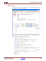
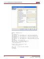
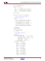
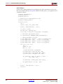
clkfx => clkfxunbuf,
clkdv => clkdvunbuf,
locked => intlock);
bufg_clk0: bufg
port map (i => clk0unbuf,
o => clk0buf);
bufg_clkfx: bufg
port map (i => clkfxunbuf,
o => clkfxbuf);
--------------------------------------------------------------------- This is the DCM reset. It is a four-cycle shift register used to
-- hold the DCM in reset for a few cycles after programming.
-------------------------------------------------------------------flop1: FDS port map (D => '0', C => clk, Q => ff1, S => '0');
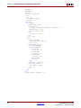
flop2: FD port map (D => ff1, C => clk, Q => ff2);
flop3: FD port map (D => ff2, C => clk, Q => ff3);
flop4: FD port map (D => ff3, C => clk, Q => ff4);
dcm_rst <= ff2 or ff3 or ff4;
------------------------------------------------------------- SysGen Component Port Mapping
-- One clock input is being connected to clk0 of the DCM,
-- and the other clock is being connected to clkfx.
-----------------------------------------------------------two_async_clks: two_async_clks
port map (
din_a => din_a,
din_b => din_b,
ss_clk_domaina_cw_ce => '1',
ss_clk_domaina_cw_clk => clk0buf,
ss_clk_domainb_cw_ce => '1',
ss_clk_domainb_cw_clk => clkfxbuf,
dout_b => dout_b);
end structural;
System Generator for DSP
Release 10.1.3 September, 2008
www.xilinx.com
123