1
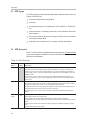
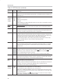
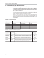
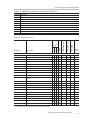
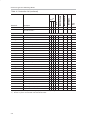
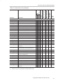
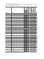
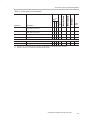
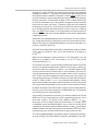
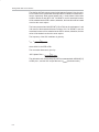
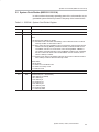
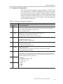
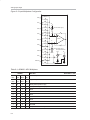
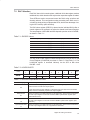
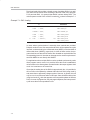
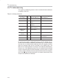
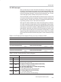
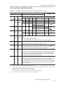
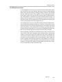
SFR Overview
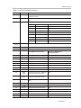
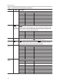
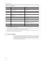
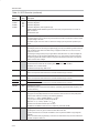
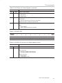
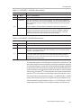
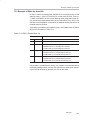
Table 3−2. SFR Overview (continued)
Name
Address
(Hex)
MWS
8Fh
Description
Memory Write Select
When bit 0 is clear (default), any writes to Flash memory via MOVX instructions are written to
data space; otherwise, writes are directed to code space.
Writing to Flash memory may be inhibited via RSL (bit 5) and PML (bit 6) in HCR0.
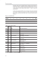
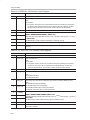
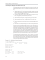
P1
90h
Port 1
Controls the byte-wide, bit-programmable input/output called Port 1. Each bit in the SFR corresponds to a pin on the actual part. Individual bits may be configured as bidirectional, CMOS output, open drain output, or input via the Data Direction SFRs for Port 1. See P1DDRL at AEh, and
P1DDRH at AFh.
Each pin may also be used to provide an alternate function and this may require particular values
in P1 and the corresponding data direction bits. For example, P1.4 may be either a general-purpose I/O bit, an input for interrupt INT2 or an active-low Slave Select (input or output) for the SPI
interface.
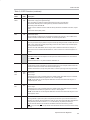
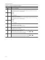
EXIF
91h
External Interrupt Flag
Four bits represent interrupt flags for interrupts INT2, INT3, INT4 and INT5 that must be cleared
manually by software. INT2 and INT4 are triggered by a rising edge, while INT3 and INT5 respond to a negative edge. If a bit is set in software, an interrupt will occur if it is enabled.
See Extended Interrupt Enable (EIE) at E8h, and Extended Interrupt Priority (EIP) at FBh
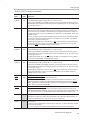
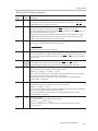
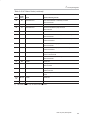
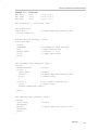
MPAGE
92h
Memory Page
During execution of MOVX @Ri,A or MOVX A,@Ri an 8-bit, low-order address may be presented
to external off-chip data memory via pins associated with Port 0.
In the MSC121x, the upper byte of a 16-bit address is placed in MPAGE. This value appears
automatically on pins associated with Port 2 when the MOVX instruction is executed.
CADDR
93h
Configuration Address Register
The MSC121x contains 128 bytes of Flash memory that may represent hardware configuration
data, such as the date of manufacture or any other identification data. This memory is distinct
from all other memory addressed by the MSC121x during normal execution of instructions. To
access this configuration data, a 7-bit address must first be written to CADDR. See CDATA at
94h.
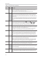
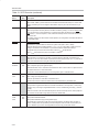
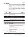
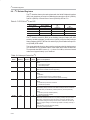
CDATA
94h
Configuration Data Register
Data in the 128 bytes of Flash hardware configuration memory is accessed via this read-only
register. The 7-bit address must first be written to CADDR at 093h.
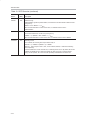
NOTE: The instruction reading CDATA must not be in Flash memory itself; otherwise, the data
read will be invalid. Typically, instructions will be executed from the internal boot ROM, SRAM
that is mapped to code space, or off-chip program memory when reading CDATA.
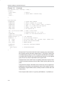
MCON
95h
Memory Configuration
Bit 7 is used to identify one of two 16-bit breakpoint registers, while bit 0 determines if the external on-chip RAM is mapped to both code and data spaces or just to data space.
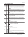
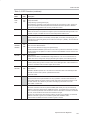
SCON0
98h
Serial Control 0
Contains six bits that determine the format of data on serial port 0 as well as two bits for transmit
and receive interrupt flags.
It is used in conjunction with TCON at 88h, TMOD at 89h and various timer data registers.
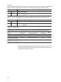
SBUF0
99h
Serial Buffer 0
When written, SFUF0 provides data for the transmitter associated with serial port 0. When read,
data is provided by the receive register. Serial data is output on pin TxD0 and received on pin
RxD0.
3-6