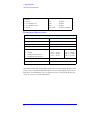
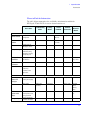
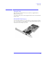
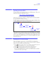
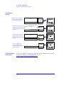
1
HP Kayak XU800 PC Workstation Technical Reference Manual Notice The information contained in this document is subject to change without notice. Hewlett-Packard makes no warranty of any kind with regard to this material, including, but not limited to, the implied warranties of merchantability and fitness for a particular purpose. Hewlett-Packard shall not be liable for errors contained herein or for incidental or consequential damages in connection with the furnishing, performance, or use of this material. Hewlett-Packard assumes no responsibility for the use or reliability of its software on equipment that is not furnished by Hewlett-Packard. This document contains proprietary information that is protected by copyright. All rights are reserved. No part of this document may be photocopied, reproduced, or translated to another language without the prior written consent of Hewlett-Packard Company. Adaptec® is a registered trademark of Adaptec, Inc. Adobe and Acrobat are trademarks of Adobe Systems Incorporated. ELSA®and Synergy® are registered trademarks of ELSA AG, Aachen and/or ELSA Inc., Santa Clara. Matrox® is a registered trademark of Matrox Electronic Systems Ltd. Microsoft®, Windows® and MS-DOS® are registered trademarks of the Microsoft Corporation. Windows NT® is a registered trademark of Microsoft Corporation. Pentium® , and AGPsetTM are trademarks of Intel Corporation. SCSISelectTM is a trademark of Adaptec, Incorporated. WOLTM (Wake on LAN) is a trademark of IBM. Hewlett-Packard France Business Desktop Division (BDD) Outbound Marketing Communications 38053 Grenoble Cedex 9 France 1999 Hewlett-Packard Company Contents 1 System Overview HP Kayak XU800 PC Workstation Overview . . . . . . . . . . . . . . . . . . . . 9 HP Kayak XU800 PC Workstation Package . . . . . . . . . . . . . . . . . . . . 13 Front and Side Views . . . . . . . . . . . . . . . . . . . . . . . . . . . . . . . . . . . . . . . . Rear View. . . . . . . . . . . . . . . . . . . . . . . . . . . . . . . . . . . . . . . . . . . . . . . . . . 13 14 Internal Features. . . . . . . . . . . . . . . . . . . . . . . . . . . . . . . . . . . . . . . . . . 14 Front Panel . . . . . . . . . . . . . . . . . . . . . . . . . . . . . . . . . . . . . . . . . . . . . . 15 Specifications and Characteristics . . . . . . . . . . . . . . . . . . . . . . . . . . . 16 Physical Characteristics . . . . . . . . . . . . . . . . . . . . . . . . . . . . . . . . . . . . . . Electrical Specifications . . . . . . . . . . . . . . . . . . . . . . . . . . . . . . . . . . . . . . Power Consumption and Cooling . . . . . . . . . . . . . . . . . . . . . . . . . . . . . . . Environmental Specifications. . . . . . . . . . . . . . . . . . . . . . . . . . . . . . . . . . 16 16 17 18 Power Saving and Ergonometry . . . . . . . . . . . . . . . . . . . . . . . . . . . . . 19 Power Saving and Ergonometry for APM Systems . . . . . . . . . . . . . . . . . Power Saving Modes and Resume Events for ACPI Systems . . . . . . . . . Power-On from Space-Bar . . . . . . . . . . . . . . . . . . . . . . . . . . . . . . . . . . . . Soft Power Down. . . . . . . . . . . . . . . . . . . . . . . . . . . . . . . . . . . . . . . . . . . . 20 20 21 21 Documentation . . . . . . . . . . . . . . . . . . . . . . . . . . . . . . . . . . . . . . . . . . . 22 Where to Find the Information. . . . . . . . . . . . . . . . . . . . . . . . . . . . . . . . . 23 3 Contents 2 System Board System Board Overview . . . . . . . . . . . . . . . . . . . . . . . . . . . . . . . . . . . . 28 Architectural View . . . . . . . . . . . . . . . . . . . . . . . . . . . . . . . . . . . . . . . . . 29 Accessory Card Slots. . . . . . . . . . . . . . . . . . . . . . . . . . . . . . . . . . . . . . . 30 Universal AGP Pro Slot . . . . . . . . . . . . . . . . . . . . . . . . . . . . . . . . . . . . . . PCI Slots . . . . . . . . . . . . . . . . . . . . . . . . . . . . . . . . . . . . . . . . . . . . . . . . . . 30 31 System Board Switches. . . . . . . . . . . . . . . . . . . . . . . . . . . . . . . . . . . . . 33 Chipset . . . . . . . . . . . . . . . . . . . . . . . . . . . . . . . . . . . . . . . . . . . . . . . . . . 34 Memory Controller Hub (8240) . . . . . . . . . . . . . . . . . . . . . . . . . . . . . . 35 Accelerated Graphics Port (AGP) Bus Interface . . . . . . . . . . . . . . . . . . AGP 4x Bus. . . . . . . . . . . . . . . . . . . . . . . . . . . . . . . . . . . . . . . . . . . . . . . . Main Memory Controller . . . . . . . . . . . . . . . . . . . . . . . . . . . . . . . . . . . . . 38 38 39 PCI 64-bit Hub . . . . . . . . . . . . . . . . . . . . . . . . . . . . . . . . . . . . . . . . . . . . 44 PCI 64-bit 66 MHz Bus Interface . . . . . . . . . . . . . . . . . . . . . . . . . . . . . . . 45 The Input/Output Controller Hub (82801AA). . . . . . . . . . . . . . . . . . . 48 Devices on the PCI 32-bit 33 MHz Bus . . . . . . . . . . . . . . . . . . . . . . . . . . Dual Chip PCI Audio Solution . . . . . . . . . . . . . . . . . . . . . . . . . . . . . . . . . Devices on the SMBus . . . . . . . . . . . . . . . . . . . . . . . . . . . . . . . . . . . . . . . Devices on the Low Pin Count Bus . . . . . . . . . . . . . . . . . . . . . . . . . . . . . The Super I/O Controller (NS 87364) . . . . . . . . . . . . . . . . . . . . . . . . . . . 53 54 55 60 61 FirmWare Hub (82802AB). . . . . . . . . . . . . . . . . . . . . . . . . . . . . . . . . . . 62 Host Bus . . . . . . . . . . . . . . . . . . . . . . . . . . . . . . . . . . . . . . . . . . . . . . . . . 64 Intel Pentium III Processor . . . . . . . . . . . . . . . . . . . . . . . . . . . . . . . . . . . Optional Second Processor . . . . . . . . . . . . . . . . . . . . . . . . . . . . . . . . . . . Cache Memory . . . . . . . . . . . . . . . . . . . . . . . . . . . . . . . . . . . . . . . . . . . . . 65 65 67 Assigned Device Interrupts . . . . . . . . . . . . . . . . . . . . . . . . . . . . . . . . . 68 Input/Output Controller Hub Interrupts . . . . . . . . . . . . . . . . . . . . . . . . . PCI 64-bit Hub Interrupts . . . . . . . . . . . . . . . . . . . . . . . . . . . . . . . . . . . . Interrupt Controllers . . . . . . . . . . . . . . . . . . . . . . . . . . . . . . . . . . . . . . . . 4 68 68 68 Contents 3 Interface Cards Graphics Cards . . . . . . . . . . . . . . . . . . . . . . . . . . . . . . . . . . . . . . . . . . . 71 Matrox Millennium G250 Graphics Card . . . . . . . . . . . . . . . . . . . . . . . . . Matrox Millennium G400 Graphics Card . . . . . . . . . . . . . . . . . . . . . . . . . 3Dlabs Oxygen GVX1 . . . . . . . . . . . . . . . . . . . . . . . . . . . . . . . . . . . . . . . . ELSA Synergy II Graphics Card . . . . . . . . . . . . . . . . . . . . . . . . . . . . . . . . 71 74 77 79 Network Cards . . . . . . . . . . . . . . . . . . . . . . . . . . . . . . . . . . . . . . . . . . . 81 HP 10/100 TX PCI LAN Interface. . . . . . . . . . . . . . . . . . . . . . . . . . . . . . . Supported LAN Cards. . . . . . . . . . . . . . . . . . . . . . . . . . . . . . . . . . . . . . . . 3COM NIC (Network Interconnect) LAN Card . . . . . . . . . . . . . . . . . . . . INTEL NIC (Network Interconnect) LAN Card . . . . . . . . . . . . . . . . . . . 81 83 83 85 4 Mass Storage Devices Flexible Disk Drives . . . . . . . . . . . . . . . . . . . . . . . . . . . . . . . . . . . . . . . . . Hard Disk Drives . . . . . . . . . . . . . . . . . . . . . . . . . . . . . . . . . . . . . . . . . . . . CD-ROM Drives . . . . . . . . . . . . . . . . . . . . . . . . . . . . . . . . . . . . . . . . . . . . . 87 87 88 5 HP BIOS HP/NBA BIOS Summary. . . . . . . . . . . . . . . . . . . . . . . . . . . . . . . . . . . . 91 Using the HP Setup Program . . . . . . . . . . . . . . . . . . . . . . . . . . . . . . . . . . 92 Updating the System BIOS. . . . . . . . . . . . . . . . . . . . . . . . . . . . . . . . . . 95 Restoring BIOS Default Settings . . . . . . . . . . . . . . . . . . . . . . . . . . . . . 95 Clearing the CMOS . . . . . . . . . . . . . . . . . . . . . . . . . . . . . . . . . . . . . . . . 96 Clearing Passwords . . . . . . . . . . . . . . . . . . . . . . . . . . . . . . . . . . . . . . . 97 Recovering the BIOS (Crisis Mode) . . . . . . . . . . . . . . . . . . . . . . . . . . 98 Adaptec SCSISelect Configuration Utility . . . . . . . . . . . . . . . . . . . . . 99 Default Settings. . . . . . . . . . . . . . . . . . . . . . . . . . . . . . . . . . . . . . . . . . . . . 99 Starting the SCSISelect Configuration Utility . . . . . . . . . . . . . . . . . . . . 101 BIOS Addresses. . . . . . . . . . . . . . . . . . . . . . . . . . . . . . . . . . . . . . . . . . 102 System Memory Map . . . . . . . . . . . . . . . . . . . . . . . . . . . . . . . . . . . . . . . . HP I/O Port Map (I/O Addresses Used by the System). . . . . . . . . . . . . 102 103 5 Contents DMA Channel Controllers . . . . . . . . . . . . . . . . . . . . . . . . . . . . . . . . . . . IRQs Used by the PC Workstation . . . . . . . . . . . . . . . . . . . . . . . . . . . . . 104 105 6 Tests and Error Messages MaxiLife Test Sequence and Error Messages. . . . . . . . . . . . . . . . . . 107 Basic Pre-boot Diagnostics . . . . . . . . . . . . . . . . . . . . . . . . . . . . . . . . . . Post Test Sequence and Post Error. . . . . . . . . . . . . . . . . . . . . . . . . . . . Operating System Boot Phase . . . . . . . . . . . . . . . . . . . . . . . . . . . . . . . . Run-Time Errors . . . . . . . . . . . . . . . . . . . . . . . . . . . . . . . . . . . . . . . . . . Main Menu . . . . . . . . . . . . . . . . . . . . . . . . . . . . . . . . . . . . . . . . . . . . . . . 108 109 110 111 112 Order in Which POST Tests Are Performed . . . . . . . . . . . . . . . . . . . 115 Error Message Summary. . . . . . . . . . . . . . . . . . . . . . . . . . . . . . . . . . . 123 Beep Codes . . . . . . . . . . . . . . . . . . . . . . . . . . . . . . . . . . . . . . . . . . . . . . . 127 7 Connectors and Sockets Rear Panel Socket Pin Layouts . . . . . . . . . . . . . . . . . . . . . . . . . . . . . 137 6 Preface This manual is a technical reference and BIOS document for engineers and technicians providing system level support. It is assumed that the reader possesses a detailed understanding of AT-compatible microprocessor functions and digital addressing techniques. Technical information that is readily available from other sources, such as manufacturers’ proprietary publications, has not been reproduced. This manual contains summary information only. For additional reference material, refer to the bibliography on the following page. For all warning and safety instructions, refer to the user guide delivered with the PC Workstation. Conventions The following conventions are used throughout this manual to identify specific numeric elements: Hexadecimal numbers are identified by a lower case h. For example, 0FFFFFFFh or 32F5h Binary numbers and bit patterns are identified by a lower case b. For example, 1101b or 10011011b 7 Bibliography Online documentation can be obtained from the HP World Wide Web site: www.hp.com/go/kayaksupport. ❒ HP Kayak XU800 PC Workstation User’s Guide D8369-900011 — as well as English, this guide is also available in various languages. ❒ HP Kayak XU800 PC Workstation Troubleshooting Guide — available in English, French, Italian, German, Spanish, Swedish and Japanese. ❒ HP Kayak XU800 PC Workstation Technical Notes — English only. ❒ HP Kayak XU800 PC Workstation Service Handbook Chapter — English only. ❒ Image Creation and Recovery CD-ROM — 5011-6692-xx2. Extra Information Can ❒ ELSA GLoria Synergy graphics card http://www.elsa.com Be Obtained At: ❒ Matrox graphics cards http://www.matrox.com ❒ 3D Labs Oxygen GVX1 graphics card http://www.3dlabs.com ❒ Intel Chipsets. Intel I840 chipset http://developer.intel.com ❒ Intel Pentium III Processor http://developer.intel.com 1. Also includes information about the HP Kayak XM600 Minitower PC Workstation. 2. xx = Language code. 8 1 System Overview This manual describes the HP Kayak XU800 PC Workstation and provides detailed system specifications. This chapter introduces the external features, and lists the specifications and characteristic data of the system. It also provides a summary of the documentation available. HP Kayak XU800 PC Workstation Overview The HP Kayak XU800 PC Workstation is based on the Extended ATX (E-ATX) form factor. The following table provides an overview of the system. Feature Description System Board E-ATX with a dimension of 12.8-inch x 11.4-inch. Processor All models have support for up to two Intel Pentium® III processors. For Processor 1, a VRM (Voltage Regulator Module) is integrated on the system board, while there is a VRM socket for a second processor. Level-One: 16 KB code, 16 KB data. Level-Two: i256 KB. Cache Memory (integrated in processor package) • Internal CPU Clock Rate External Processor Bus 533 MHz, 600 MHz, 667 MHz, 733 MHz, 800 MHz and higher. 133 MHz Front Side Bus. Chipset Intel® Chipset (I840) including, Input/Output Controller Hub (ICH), PCI 64-bit Hub (P64H), FirmWare Hub (FWH) and Memory Repeater Hub (MRH-S) for SDRAM support. Super I/O Chip NS 87364. BIOS (Basic Input/Output System) Based on the core of AMIBIOS, including: • • • • Firmware - BIOS 4 M/bits of flash memory. Support for PCI 2.2 Specification. Support for RDRAM or SDRAM memory modules. Flash EEprom: Intel’s Firmware hub concept. 9 1 System Overview HP Kayak XU800 PC Workstation Overview Feature Description HP MaxiLife Utility (available on all models) Hardware monitoring utility that monitors system components via the I2C bus and a LCD status panel. Operating System All models are preloaded with Windows NT® 4.0 SP5. Main Memory Maximum amount of memory that can be installed is: 2 GB (4 x 512 MB) Models include either: • • Mass Storage Seven shelves supporting: • • • SCSI Controller IDE Controller 10 Four RIMM sockets supporting RDRAM ECC memory modules installed in pairs. Any unused RIMM sockets must contain a continuity module. Models are supplied with either 128 MB or 256 MB RDRAM ECC main memory installed in pairs. Memory upgrades are available in pairs of: 64 MB, 128 MB, 256 MB or 512 MB RDRAM ECC modules. Four DIMM sockets supporting SDRAM 100 MHz ECC memory modules installed in pairs. Models are supplied with 128 MB of SDRAM unbuffered ECC main memory. Memory upgrades are available in pairs of: 64 MB, 128 MB, 256 MB or 512 MB unbuffered 100 MHz ECC SDRAM modules. Two front-access, third-height 3½-inch (one for the floppy disk drive and one free) (height 1”); Three front-access, half-height, 5¼-inch drives (height 1.0”); Possibility of installing a 3½-inch hard disk drive in one of the 5¼-inch shelves. Two internal 3½-inch hard disk drives (height 1.0”). Ultra 160 SCSI controller: Adaptec® AIC-7892 Ultra 160 16-bit integrated SCSI controller (160 MB/s). The internal SCSI connectors allow for up to five internal devices to be connected. Additional devices can be added outside the PC Workstation by connecting directly to the rear panel SCSI connector. The external connector allows up to ten external devices to be connected. This gives a maximum of 15 (internal + external) devices that can be connected. All models include an integrated Ultra ATA-66 controller that supports up to four IDE devices. 1 System Overview HP Kayak XU800 PC Workstation Overview Feature Video Controllers Description Models include either: • • • • Accessory Card Slots ELSA GLoria Synergy® II AGP video controller with 32 MB of installed SGRAM video memory (maximum configuration). Matrox® Millennium G250 AGP video controller with 8 MB SGRAM video memory which can be upgraded to 16 MB. Matrox Millennium G400-Dual monitor AGP video controller with 16 MB SGRAM video memory (maximum configuration). 3Dlabs Oxygen® GVX1, 32 MB SGRAM video memory (maximum configuration). All models have: One Universal AGP Pro 4X 50 W 32-bit slot. The AGP bus provides a high performance graphics interface. 1 • Three 32-bit 33 MHz PCI slots: 1, 2 and 5 (5 V). • Two 64-bit 66 MHz PCI slots: 3 and 4 (3.3 V). The majority of the configurations are delivered with PCI slots 1 to 4 vacant. • LAN Card All models are supplied with an HP 10/100BT PCI Ethernet Adapter LAN card installed in PCI slot 5, supporting Wake-On LAN (WOL) and PCI 2.2 Specification. CD-ROM Drive Models include either an IDE 48X CD-ROM, CD-RW drive or DVD drive. Audio Integrated on the system board CS4280 audio PCI chip and AC97 Codec (CS4297) audio. HP UltraFlow Cooling System Cooling system with multiple temperature-regulated fans to optimize cooling. Alert reporting to MaxiLife and TopTools. 1. All five PCI slots comply with the PCI Specification 2.2. 11 1 System Overview HP Kayak XU800 PC Workstation Overview Feature System Board Connectors Rear Panel Connectors (color coded) Description One flexible disk drive connector Two ATA-66 IDE connectors (for up to four IDE devices) • One 16-bit Ultra 160 SCSI connector and one SCSI terminator. The SCSI cable is routed from the SCSI connector on the system board (located near the system switches) to the SCSI devices inside the chassis, onto an onboard SCSI terminator (behind the processor), and finally onto the external SCSI connector on the rear panel. The onboard SCSI terminator is automatically deactivated when an external device is attached. • One CD-IN audio connector • AUX connector • Internal speaker connector • One WOL connector • One status panel connector • Two power supply connectors that must be connected • Two fan connectors (one for the PCI fan, and one for the rear fan) • One battery socket The system board layout with all connectors can be found on page 28. • • 9-pin serial (two, buffered) ❒ Standard: Two UART 16550 buffered serial ports (both RS-232-C). ❒ Serial Ports A and B: 2F8h (IRQ 3), 2E8h (IRQ 3), 3F8h (IRQ 4), 3E8h (IRQ 4), or Off— (if one port uses 2xxh, the other port must use 3xxh). • • • • • • 12 Dual USB connectors External 16-bit U160m SCSI connector Audio ❒ Joystick/Dual MIDI connector ❒ LINE IN jack (3.5 mm) ❒ LINE OUT jack (3.5 mm) ❒ MIC IN jack (3.5 mm) Keyboard/Mouse ❒ HP enhanced keyboard with mini-DIN connector ❒ HP enhanced scrolling mouse with mini-DIN connector 25-pin parallel connector ❒ Mode: Centronics or bidirectional modes (ECP/EPP) ❒ Parallel port: 1 (378h, IRQ 7), 2 (278h, IRQ 5), or Off. 1 System Overview HP Kayak XU800 PC Workstation Package HP Kayak XU800 PC Workstation Package The following two diagrams show the front and rear views of the HP Kayak XU800 PC Workstation. Front and Side Views Power Supply Unit HP UltraFlow Airflow Guide Front Access Drives, for - three 5.25-inch drive shelves. Possibility of installing a 3½-inch hard disk drive in one of the 5¼-inch shelves. - two 3.5-inch shelves including a 1.44 MB floppy disk drive Rear Fan Spare mounting rails (not shown) for: - 3.5-inch (short green) devices (for example, zip drive), - 5.25-inch (long green) devices, - 3.5-inch (short blue) hard disk drives Primary Internal Hard Disk Drive Shelf Secondary Internal Hard Disk Drive Shelf Second 3.5-inch shelf 13 1 System Overview Internal Features Rear View External SCSI connector Keyboard connector Mouse connector Dual USB (12 Mbps) connectors Serial port A Serial port B Line Out connector Line In connector Microphone connector Parallel port Display connector MIDI connector Internal Features The core architecture of the HP Kayak XU800 PC Workstation is constructed around: Memory Controller Hub (MCH), Input/Output Controller Hub (ICH), FirmWare Hub (FWH) and the Host bus. The HP Kayak XU800 PC Workstation can support up to two Pentium III processors. This processor is described on page 65. The components of the system board are described in chapter 2; the characteristics of the PC Workstation’s video and storage devices are described in chapter 3; mass storage devices are described in chapter 4; the HP BIOS routines are summarized in chapter 5; and the Power-On Self-Test routines are described in chapter 6. 14 1 System Overview Front Panel Front Panel The front panel of HP Kayak XU800 PC Workstation has the following features: LCD Control Buttons Power On/Off Button Reset Button Hard Disk Activity Light • Liquid Crystal Display (LCD). LCD error messages and available menus are described on page 107. • On/Off LED. There are five states: Blank. Indicates that the computer is turned off. Green. Indicates that the computer is turned on and running correctly. Red. Indicates that there is a Power-On Self-Test (POST) error. Red flashing. Indicates that there is a MaxiLife (Diag/Alarm) error. Amber. Displayed during system reset, system lock, Standby mode (Windows 98) or Suspend mode (Windows 95). • Hard disk drive activity LED. Activated during POST and when the hard disk drive is being accessed. 15 1 System Overview Specifications and Characteristics Specifications and Characteristics Physical Characteristics System Processing Unit Weight (excl. keyboard and display): 14.4 kilograms (31.68 pounds) Dimensions: 47.0 cm max. (D) by 21,0 cm (W) by 49.0 cm (H) (18.50 inches by 8.26 inches by 19.29 inches) Footprint: 0.09 m2 (1.06 sq ft) Electrical Specifications Parameter Total Rating Input voltage Switch select Input current (max) 2. 3. Maximum per PCI Slots1 (1,2 & 5) 32-bit 33 MHz Maximum per PCI Slots1 (3 & 4) 64-bit 66 MHz Maximum for Universal AGP Pro Slot2 100 - 127 VAC 200 250 V Vac — — — — 9A 4.5 A — — — — — — — Input frequency 50 to 60 Hz — Available power 300 W 320 W Max current at +12 V 13.5 A 15 A 0.5 A 0.5 A 9.2 A Max current at -12 V 0.8 A — 0.1 A 0.1 A — Max current at +3.3 V 1.5 A — 7.6 A 7.6 A Imax(Vcc) = 7.6 A Max current at Vddq (3.3 V or 1.5 V) — — — — Imax(Vddq) = 2 A Max current at +5 V 32 A — 5A 5A 2A Max current at -5 V 0.5 A — — — — 2A — Max current at +5Vstdby3 combined with 3.3 V stdby 1. Peak (15 secs.) 100 W for PCI slots and AGP Pro slot 1.5 A total on 3.3 V stdby The maximum power dissipation for a PCI card is 25 W (refer to PCI specifications 2.2 on page 31). An AGP Pro card uses the electrical and cooling resources of both the Universal AGP Pro slot and the adjacent PCI slot. Power limitation is managed in the BIOS. Refer to System Board Switch 10 on page 33. 16 1 System Overview Specifications and Characteristics Some examples of a supported configuration with combined power consumption of 100 W (PCI slots + Universal AGP Pro slot): Number of PCI Accessory Cards AGP Pro Slot Total Power Supply Used Accessory Card Power Consumption One AGP Pro Card (50 W) 1 x 5 W PCI accessory card + 3 x 15 W PCI accessory cards + 0 W empty PCI slot (adjacent to Universal AGP Pro slot) + 1 x 50 W AGP Pro card 100 W One AGP Pro Card (50 W) 1 x 5 W PCI accessory card + 1 x 15 W PCI accessory card + 2 x 12.5 W PCI accessory cards+ 0 W empty PCI slot (adjacent to Universal AGP Pro slot) + 1 x 50 W AGP Pro card 100 W Four Five One AGP Standard Card (25 W) 1 x 5 W PCI accessory card + 2 x 25 W PCI accessory cards + 2 x 10 W PCI accessory cards + 1 x 25 W AGP standard card 100 W Four An attempt to draw too much current (such as a short circuit across edgeconnector pins, or an accessory board that is not suitable for this PC Workstation), will cause the overload protection in the power supply to be triggered, and will shut down the PC Workstation. NOTE When the PC Workstation is turned off with the power button on the front panel, the power consumption falls below the low power consumption (refer to the following table), but is not zero. The special on/off method used by this PC Workstation extends the lifetime of the power supply. To reach zero power consumption in “off” mode, either unplug the PC Workstation from the power outlet or use a power block with a switch. Power Consumption and Cooling The power consumption and acoustics (shown in the Environmental Specifications table) are valid for a standard configuration as shipped (one processor, 256 MB of memory, 300 W power supply, one hard disk drive, video card, LAN card). All information in this section is based on primary power consumptions. Power consumption - Windows NT: • • • 1. Operating with input/output (disk access) Operating without input/output (idle) Off with LAN card 230 V / 50 Hz 115 V / 60 Hz 85.5 W - 291.7 Btu/h1 84.5 W - 288.3 Btu/h 77.2 W - 263.4 Btu/h 4 W - 13.6 Btu/h 75.8 W - 258.6 Btu/h 4.2 W - 14.3 Btu/h 1 W = 3.4121 Btu/h 17 1 System Overview Specifications and Characteristics Component: • • • • Processor: SCSI HDD with access: SCSI HDD with no access: PCI card: 50 W 23 W 16 W 10 W - 36 W - 170.6 Btu/h 78.4 Btu/h 54.5 Btu/h 34.1 Btu/h - 122.8 Btu/h Environmental Specifications Environmental Specifications (System Processing Unit, with Hard Disk) Operating Temperature +10 °C to +35 °C (+50 °F to +95 °F) Storage Temperature -40 °C to +70°C (-40 °F to +158 °F) Operating Humidity 15% to 85% (relative)1 Storage Humidity 8% to 85% (relative)1 Acoustic noise emission (as defined ISO 7779): • • • Operating Operating with hard disk access Operating with floppy disk access Sound Power LwA <= 43.9 dB LwA <= 44.9 dB LwA <= 46.7 dB Operating Altitude 10000 ft (3100m) max Storage Altitude 15000ft (4600m) max Sound Pressure LpA <= 30.8 dB LpA <= 31.8 dB LpA <= 33.6 dB 1.non condensing conditions. Operating temperature and humidity ranges may vary depending upon the mass storage devices installed. High humidity levels can cause improper operation of disk drives. Low humidity levels can aggravate static electricity problems and cause excessive wear of the disk surface. 18 1 System Overview Power Saving and Ergonometry Power Saving and Ergonometry Depending on the operating system, the following power management types are available: • No sleeping state: Windows NT 4 (Full On and Off). • APM: Windows 95 and Windows 98 SE APM (Full On, Standby, Suspend and Off). • ACPI: Windows 98 SE ACPI and Windows 2000 (Full On, S1, Suspend to RAM, Suspend to disk, Off). Windows 2000 A P M Windows 98 SE Windows NT 4 Windows 95 Full On Supported Supported Supported Standby Supported Suspend Not Supported by Windows 2000 Off A C P I 1. Supported Supported Not Supported by Windows NT 4 Supported Supported Supported Supported S1 (processor stopped) Supported Supported S31(suspend to RAM) Supported Supported S4 (suspend to disk / hibernation) Supported Not Supported by Windows 98 S5 (off) Supported Supported APM only Operating System It is anticipated that the S3 feature will be supported by HP Windows 2000 models. More information about this feature will be documented with the HP Windows 2000 release. 19 1 System Overview Power Saving and Ergonometry Power Saving and Ergonometry for APM Systems Standby1 Full On Off Normal speed Normal speed Halted Halted On Blanked, <30 W, on models with integrated graphics Blanked, <5 W (typ) Blanked, <5 W (typ) Normal speed Stopped Halted Halted supports up to 300 W <40 W (230V, 50 Hz) <27 W (115V, 60 Hz) <40 W (230V, 50 Hz) <21 W (115V, 60 Hz) (plugged in but turned off) <5 W (average) Resume events Keyboard, mouse, alarms, LAN, modem, USB Keyboard, network (RWU), modem, USB Space bar or power button, RPO Resume delay Instantaneous a few seconds Boot delay Processor Display Hard disk drive Power consumption 1. Suspend1 Not supported by Windows NT 4. Power Saving Modes and Resume Events for ACPI Systems Full On S1 Suspend to RAM Suspend to Disk Off Processor Normal speed Halted Off Off Off Display On Blanked Off Off Off Hard Disk Drive Normal speed Halted Off Off Off Active Power Planes VCC VCCAux VCC VCCAux Memory VCCAux VCCAux VCCAux Power Consumption Supports up to 300 W <40 W <10 W <10 W <10 W Power button, LAN, Modem, Scheduler, HP Start Key Power button, LAN, Modem, Scheduler, HP Start Key Power button, HP Start Key Resume Events Power button, LAN, Modem, USB, Scheduler, HP Start Key Resume Delay Instantaneous Instantaneous BIOS boot delay Regular boot delay 20 1 System Overview Power Saving and Ergonometry Power-On from Space-Bar The power-on from the space-bar function is enabled provided that: • The computer is connected to a Power-On keyboard (recognizable by the Power-On icon on the space bar). • The function has been enabled by setting SW-7 to up (default setting) on the system board switches. • The function has been enabled in the “Power” menu of the Setup program (default configuration). Soft Power Down When the user requests the operating system to shut down, the environment is cleared, and the computer is powered off. Soft Power Down is available with the Windows NT operating system. 21 1 System Overview Documentation Documentation The table below summarizes the availability of the documentation that is appropriate to the HP Kayak XU800 PC Workstation. Only selected publications are available in paper-based form. Most are available as printable files from the HP division support servers, or from the HP website. Title PDF file Shipped with the PC Workstation1 HP Kayak XU800 Troubleshooting Guide PDF file2 PDF file No HP Kayak XU800 Training Module CD-ROM No No HP Kayak XU800 Technical Reference Manual PDF file (this document) PDF file No PDF file PDF file When available, it will be included in the fourth edition of the Service Handbook PDF file PDF file No HP Kayak XU800 Service Handbook Chapter HP Kayak XU800 Technical Notes 2. Paper-based PDF file HP Kayak XU800 User’s Guide 1. Online at HP WWW Site (see address below) Division Support Server Refer to the Service Handbook Chapter for the availability of the localized monolingual and multilingual User’s Guides. Also available in French, Italian, German, Spanish, Swedish and Japanese. Access HP World Wide Web Site Additional online support documentation, BIOS upgrades and drivers are available from HP’s World Wide Web site, at the following address: World-Wide Web URL: http://www.hp.com/go/kayaksupport then select HP Kayak XU800 PC Workstation. 22 1 System Overview Documentation Where to Find the Information The table below summarizes the availability of information within the HP Kayak XU800 PC Workstation documentation set. User’s Guide Troubleshooting Guide1 Service Handbook Technical Information Technical Reference Manual Exploded view. Parts list. Configuration. Key features. HP Web sites. HP Web sites. HP Web sites, others. Basic details. Advanced. Advanced. Memory maps. Technical details. Memory maps. Complete list. Training Module Introducing the PC Product features Standard configuration. New features. Product range. CPL dates. Product model numbers Environmental Setting up the PC. Working in comfort. Safety Warnings Electrical, multimedia, safety, unpacking, removing & replacing cover. Safety. Finding on-line information Preloaded, HP Web sites. HP Web sites. Technical information Basic details. Formal documents Certificate of Conformity. Software License agreement. Using the PC Connecting devices and turning on Rear panel connectors, starting and stopping. Basic details. Updating and recovering. New features. Fields and their options within Setup Basic details. Viewing Setup screen, using, passwords Basic details. New fields. Manageability Power management, Software and drivers. BIOS 23 1 System Overview Documentation User’s Guide Troubleshooting Guide1 Training Module Service Handbook Technical Information Technical Reference Manual Upgrading the PC Opening the PC Full description. New procedures. Full PN details Supported accessories Installing accessories Configuring devices System board Processor(s), memory, accessory boards, mass storage devices. Installing devices Error messages, problem solving. Installing and removing, connectors and switch settings. Switch settings. Full PN details New procedures. Installing devices. Network connection. Jumpers, switches, connectors and replacing. Jumpers, switches and connectors. Layout and switch settings. Jumpers, switches and connectors. Chip-set details. Repairing the PC Troubleshooting Power-On SelfTest routines (POST) Kayak diagnostic utility Basic, MaxiLife, hardware diagnoses. MaxiLife, hardware diagnoses and suggested solutions. Repair policy. Basic details. Error Messages, EMU and suggestions for corrective action. New features. HP DiagTools, CD-ROM recovery. HP DiagTools, CD-ROM recovery New features Peripheral Devices Audio Accessories Refer to Audio User’s Guide for information on setting up and configuring audio accessories. 24 Refer to online version of Audio User’s Guide for information on setting up and configuring audio accessories. Service notes. Advanced. Error codes and suggestions for corrective action. Order of tests. Technical details. 1 System Overview Documentation User’s Guide LAN Accessories 1. Refer to LAN Administrator’s Guide for information on setting up and configuring LAN cards and systems. Troubleshooting Guide1 Training Module Service Handbook Technical Information Technical Reference Manual Refer to online version (preloaded on hard disk) of LAN Administrator’s Guide for information on setting up and configuring LAN cards and systems. For address, “Access HP World Wide Web Site” on page 22. 25 1 System Overview Documentation 26 2 System Board This chapter describes the components of the system board, taking in turn the components of the Memory Controller Hub (MCH), the Input/Output Controller Hub (ICH), FirmWare Hub (FWH) and the Host Bus. The following diagram shows in detail the HP Kayak XU800 PC Workstation Extended ATX (E-ATX) system board. 11 .4inc hes wi de i .8- es nch h hig 12 27 2 System Board System Board Overview System Board Overview The following diagram shows where the different chips and connectors are located on the E-ATX system board. Fan CPU 1c - J17 SCSI Termination Connector - J23 AUX Power- J31 Power Supply - J47 Mouse (upper) & Keyboard (lower) - J3 FDD - J38 Two USB - J8 Processor 1 Connector - XU3 Serial Port A - J5 Serial Port B - J4 (Both ports are stacked with the Parallel Port) Secondary IDE - J44 Primary IDE - J37 Processor 2 Connector - XU2 Rear Fan- J18 Line Out Line In MIC Midi & Audio - J2 Anti-Intrusionb - J10 XU1 Memory Expansion Card Card ConnectorsConnectors - XU1,J22 XU4 Memory Controller Hub (MCH) 8284O-QP - U24 Input/Output Controller Hub (ICH) 82801AA- U34 Fan CPU2c - J19 XU4 Universal AGP PRO Slot - J22 PCI Slot 1 (32-bit 33 MHz, 5V) - J15 PCI Slot 2 (32-bit 33 MHz, 5V) - J14 Super I/O NS 87364 Chip - U6 socket VRM for CPUfor 2 - J45 CPU2 - J45 Battery - XU6 HDD Temperature Sensor - J56 Battery - XU6 PCI Fan - J50 CD-ROM Audio In - J52 AUX Audio In - J51 Internal Speaker- J48 MaxiLife U25 Status Panel - J43 Internal SCSI U160 Connector to Internal Devices - J43 Adaptec 7892 SCSI U160 Controller - U44 CS4280 Audio PCI chip- U7 PCI Slot 5 (32-bit 33 MHz, 5V)- J11 PCI Slot 4 -J14 (64-bit 66 MHz, 3.3V) Wake-On Lanc PCI 64-bit Hub (WOL)- J26 (P64H)- U32 PCI Slot 3 - J13 (64-bit 66 MHz, 3.3V) Additional SCSI LED Connector J25 FirmWare Hub Controller (FWH) 82802AB- U35 Configuration Switches - SW1a a. Refer to “Switch Boxes” on page 33 or the Switch Block Label located on the chassis of the system box for the different system board switch settings. b. Connector for the Anti-Intrusion switch. c. Optional. d. Connector for additional control of HDD LED on the status panel through the SCSI controller on a PCI add-on card. 28 2 System Board Architectural View Architectural View Intel Pentium III Processor (optional second processor) with L2 cache memory Intel Pentium III Processor with L2 cache memory SECC-2 cartridge Address (36) Control Host (also called FSB) Bus 100/133 MHz, 1 GB/sec data transfer rate) Data (64) AGP 4x Bus (133 MHz (1 GB MB/s data Universal transfer rate) AGP PRO HUB Connector LINK 16 PCI Bus (64-bit, 66 MHz) 533 MB/s data transfer rate Onboard AIC7892 SCSI U160 Controller Parallel and Serial Ports I840 Memory Controller Hub (MCH) 82840-QP Dual Rambus Channel (2.4 GB/s at 300 MHz or 3.2 GB/s at 400 MHzdata transfer rate) Memory Expansion Card Connector (533 MB/s data transfer rate) HUB LINK 8 (266 MB/s data transfer rate) PCI 64-Bit Hub (P64H) Slot 3 - 64-bit/66 MHz Slot 4 - 64-bit/66 MHz I/O Controller Hub (ICH) 82801AA 2 IDE Connectors ATA 66, 2 Channels IDE Controller 2 USB Connectors USB 2 x USB Controller Super I/O NS 87364 LPC / FWH Link PCI Bridge AC’97a Audio Controller SM Bus Controller LPC Bridge PCI Bus (32-bit, 33 MHz) 133 MB/s data transfer rate Slot 1 - 32-bit/33 MHz Slot 2- 32-bit/33 MHz Slot 5 - 32-bit/33 MHz SMBus Keyboard, Mouse and Floppy SECC-2 cartridge FirmWare Hardware (FWH) 82802 Serial EEPROM MaxiLife Monitoring Chip Audio PCI Chip (CS4280) AC ‘97 Digital Link Fans LCD Status Panel MIDI Port Codec Audio AC‘97 a. It should be noted that the AC’97 Audio Controller is not used. The PCI CS4280 and CS4297 audio is a full PCI solution that is independent of the ICH core logic. 29 2 System Board Accessory Card Slots Accessory Card Slots The following block diagram shows the position of the accessory card slots on the system board. One Universal AGP Pro slot. Used for a graphics controller. (Universal AGP Pro Slot) - J22 Three 32-bit 33 MHz PCI slots: PCI Slot 1, PCI Slot 2, PCI Slot 5 (PCI Slot 1) - J15 (PCI Slot 2) - J14 (PCI Slot 3) - J13 Two 64-bit 66 MHz PCI slots: PCI Slot 3, PCI Slot 4 (PCI Slot 4) - J12 (PCI Slot 5) - J11 System board edge Universal AGP Pro Slot The Universal AGP Pro (Accelerated Graphics Port) bus, provides a high-performance graphics interface. It uses a 66.6 MHz base clock, and provides a peak bandwidth of 1064 MB/second in AGP 4x mode. The Universal AGP Pro slot is a Universal-type connector which provides power through 3.3 V, 12 V or 5 V power rails with a maximum allocated power consumption of 50 W. The Universal AGP Pro slot supports AGP 1x and 2x modes (uses 3.3 V or 1.5 V signals), and AGP 4x mode (1.5 V signalling is required). AGP Video Card1 Supported operation in the Universal AGP Pro Slot 1.5 V ≤ 25 W ≤ 50 W 3.3 V ≤ 25 W ≤ 50 W AGP1x2 yes yes yes yes yes yes 2 yes yes yes yes yes yes 2 AGP4x yes yes yes yes no no PCI-type yes yes yes yes yes yes AGP2x 1. AGP Pro video cards are supported up to 50 W. 2. With or without sideband addressing. 30 Universal ≤ 25 W ≤ 50 W 2 System Board Accessory Card Slots AGP 4x mode transfers data at twice the speed of AGP 2x mode, which is itself twice the speed of the basic AGP 1x mode. This is achieved by multiplying the 66 MHz AGP clock frequency, so that four packets of data are transferred on each cycle (transfers on both rising and falling edges of the clock speed). Each packet of data contains four bytes, giving a transfer rate of 66.6 MHz x 4 (quad-clock mechanism) x 4 bytes, a maximum bandwidth of 1064 MB/s. The AGP interface and bus are explained on page 38. PCI Slots There is a total of five Peripheral Component Interconnect (PCI) connectors on the system board: Three 32-bit 33 MHz PCI slots: 1, 2 and 5. • Two 64-bit 66 MHz PCI slots: 3 and 4. • The three 32-bit/33 MHz PCI slots accept 5 V PCI cards and Universal PCI cards (support for 3.3 V or 5 V), while the two 64-bit/66 MHz PCI slots support 3.3 V PCI cards and Universal PCI cards (support for 3.3 V or 5 V). A universal compatible 32-bit 33 MHz accessory card can also be installed in PCI slots 3 or 4. However in this case the PCI 64-bit bus will only perform at 33 MHz. The maximum supported power consumption per slot is 25W, from the 5V and/or the 3.3V supply, and must respect the electrical specifications of the PCI 2.2 specification. The power consumption of each PCI board is automatically reported to the system through the two Presence Detect pins of each PCI slot. These pins code the following cases: • • • • No accessory board in the PCI slot. 7 W maximum PCI board in the PCI slot. 15 W maximum PCI board in the PCI slot. 25 W maximum PCI board in the PCI slot. If a standard AGP (Accelerated Graphics Port) card is installed in the AGP Pro slot, the maximum power consumption for the PCI accessory and AGP slot must not exceed 100 W. 31 2 System Board Accessory Card Slots If an AGP Pro card (>25 W and ≤50 W) is installed, then the PCI slot 1 is made inaccessible as defined in the AGP Pro specification (PCI slot must be left unoccupied to provide its sources, in terms of cooling and electrical power, to the AGP Pro card. The following table shows the various PCI board installations for the different PCI slots: PCI Card 5 V 32-bit/ 33 MHz 64-bit/ 33 MHz 32-bit/ 33 MHz or 66 MHz 64-bit/ 33 MHz or 66 MHz Slots 1, 2 & 5 5 V, 32-bit/33 MHz yes yes1 not supported not supported Slots 3 and 4 3.3 V, 64-bit/66 MHz not supported not supported PCI Slot 1. 2. 3. 4. Universal (3.3 V or 5 V compatible) 3.3 V 32-bit/ 33 MHz or 66 MHz 64-bit/ 33 MHz or 66 MHz yes yes2 yes1 yes1,2 33 MHz 66MHz 33 MHz 66 MHz 33 MHz 66 MHz 33 MHz 66 MHz yes3,4 yes4 yes3 yes yes3,4 yes4 yes3 yes A 64-bit card can be installed in a 32-bit slot. However, this card will only operate in 32-bit mode. A 66 Mhz card can be installed in a 33 MHz slot. However, this card will only operate in 33 MHz mode. A 33 MHz card can be installed in a 66 MHz slot, However, the card will operate in 33 MHz mode and will force all other PCI devices to operate at 33 MHz as well. A 32-bit card can be installed in a 64-bit slot without preventing other 64-bit PCI devices to operate in 64-bit mode. The system board and BIOS support the PCI specification 2.2. This specification supports PCI-to-PCI bridges and multi-function PCI devices, and each of the five PCI slots have Master capabilities. PCI slots 1, 2 and 5 are connected to the ICH PCI 32-bit 33 MHz bus, while PCI slots 3 and 4 are connected to the PCI 64-bit 66 MHz bus via the P64H. In addition to these PCI slots, the following devices are also connected to a PCI Bus: PCI 32-bit/33 MHz Bus PCI 64-bit/66 MHz Bus ICH (Input/Output Controller Hub) chip, bridge between the MCH (Memory Controller Hub), USB ports and IDE buses. Digital audio CS4280 controller. Onboard AIC7892 SCSI U160 controller. The PCI 64-bit 66 MHz bus is explained on page 45. The PCI 32-bit 33 MHz bus is explained on page 53. 32 2 System Board System Board Switches System Board Switches There are ten system board switches used for configuration, numbered from 1 to 10. Of these a certain number are reserved and should not be modified, otherwise it could lead to a system failure. Switch Default Position 1 UP 2 UP1 3 UP 4 UP 5 UP1 6 DOWN1 7 DOWN1 8 DOWN1 9 DOWN1 10 1. Switch Boxes UP1 Function: UP enables normal mode. DOWN enables the BIOS recovery mode at next boot. UP allows Processor(s) to automatically choose the FSB speed. DOWN forces the FSB speed to 100 MHz. UP enables User and System Administrator passwords. DOWN clears the passwords at next boot. UP retains CMOS memory. DOWN clears CMOS memory at next boot. UP = Automatic FSB frequency setting. DOWN = Sets operation to 133 FSB/300 Rambus. UP. AGP¨110 W cards appear as 50 W. DOWN enables AGP 110 W detection. UP disables keyboard power-on. DOWN enables keyboard power-on. UP forces the PCI 64 bus to 33 MHz if slots 3 and 4 are empty. DOWN disables this option. UP disables this option. DOWN enables spread spectrum clocking. UP Disables this option. DOWN provides 3.3 V Stdby to AGP Pro connector. These are default settings and should not be changed. There are two types of system board switch boxes that may be used on the HP Kayak XU800 PC Workstation. Default Configuration or OPEN = UP CLOSED = DOWN 10 9 OFF = OPEN ON = CLOSED UP = OPEN X DOWN = CLOSED X 8 7 6 4 3 2 X X 5 X X X 1 X X X 33 2 System Board Chipset Chipset The Intel® I840 chipset is a high-integration chipset designed for graphics/ multimedia PC platforms and is comprised of the following: P64H FWH ICH MCH • The 82840 Memory Controller Hub (MCH) is a bridge between: the Host bus, Dual Rambus bus (main memory), the PCI bus (64-bits/66 MHz), AGP 4x (graphic) bus, Hub Link 8-bit and Hub Link 16-bit, and the PCI 64-bit Hub (P64H). The MCH chip feature is described in detail on page 35. • The PCI 64-bit Hub (P64H) performs PCI bridging between the MCH and the PCI 64-bit 66 MHz bus. The P64H is described in detail on page 44. • The 82801AA Input/Output Controller Hub (ICH) is a bridge between the following buses: the PCI bus (32-bits/33 MHz) and SMBus. In addition, the ICH supports the integrated IDE controller (Ultra ATA/66), Enhanced DMA controller, USB controller, Interrupt controller, Low Pin Count (LPC) interface, FWH interface, ACPI Power Management Logic, AC’97 2.1 Compliant Link, AOL (Alert-On-LAN) and Real Time Clock (RTC) and CMOS. The ICH is described in detail on page 48. • 34 The 82802AB Firmware Hub (FWH) stores system BIOS and SCSI BIOS, nonvolatile memory component. In addition, the FWH contains an Intel® Random Number Generator (RNG). The RNG provides random numbers to enable fundamental security building blocks for stronger encryption, digital signing and security protocols for the PC Workstation. The FWH is described in detail on page 62. 2 System Board Memory Controller Hub (8240) Memory Controller Hub (8240) The MCH Host Bridge/Controller is contained in a 544-pin Ball Grid Array (BGA) package and is the bridge between the Host bus, Dual Rambus bus (main memory), AGP 4x (graphic) bus, Hub Link 8-bit and Hub Link 16-bit. The following figure shows an example of the system block diagram using the MCH. Intel Pentium III Processor (optional second processor) with L2 cache memory Intel Pentium III Processor with L2 cache memory SECC-2 cartridge Address (36) Control Host (also called FSB) Bus 100/133 MHz, 1 GB/sec data transfer rate) Data (64) Universal AGP PRO Connector SECC-2 cartridge AGP 4x Bus (133 MHz (1 GB MB/s data transfer rate) HUB LINK 16 I840 Memory Controller Hub (MCH) 82840-QP AGP Dual Rambus Bus Memory Interface Controller (2.4 GB/s at 300 MHz or 3.2 GB/s at 400 MHzdata transfer rate) Memory Expansion Card Connector (533 MB/s data transfer rate) PCI Bus (64-bit, 66 MHz) 533 MB/s data transfer rate P64H PCI Interface Onboard AIC7892 SCSI U160 Controller Slot 3 - 64-bit/66 MHz Slot 4 - 64-bit/66 MHz HUB LINK 8 (266 MB/s data transfer rate) I/O Controller Hub (ICH) 82801AA 35 2 System Board Memory Controller Hub (8240) The following table shows the features that are available in the MCH Host Bridge/Controller. Feature • Processor/Host Bus: ❒ Supports up to two Pentium III processors at: 100 MHz/133 MHz Host Bus frequency. ❒ Supports full Symmetric Multiprocessor (SMP) Protocol for up to two processors. ❒ Provides an 8-deep In-Order Queue supporting up to eight outstanding transaction requests on the host bus. ❒ Desktop optimized GTL+ bus driver technology (gated GTL+ receivers for reduced power). ❒ Support for 36-bit host bus address. ❒ IERR and BERR signals generate SCi/SERR. ❒ Parity protection on address and resource signals: Parity errors generate SERR. • Memory Controller. Direct Rambus: Feature • SDRAM: ❒ Dual Direct Rambus Channels operating in lock-step (both channels must be populated with a memory module). Supporting 300 MHz or 400 MHz. ❒ RDRAM 64 Mb, 128 Mb, 256 Mb devices. ❒ Minimum upgrade increment of 16 MB using 64 Mb DRAM technology. ❒ Up to 64 Direct Rambus devices (without using MRH-R). Dual channel maximum memory array size is: — 512 MB using 64 Mb DRAM technology. — 1 GB using 128 Mb DRAM technology. — 2 GB using 256 Mb DRAM technology. ❒ Up to 8 simultaneous open pages: — 1 KByte page size support for 64 Mbit, 128 Mbit and 256 Mbit RDRAM devices. — KByte page size support for 256 Mbit RDRAM devices. • Accelerated Graphics Port (AGP) Interface: ❒ Single Universal AGP PRO connector. ❒ AGP Rev 2.0 compliant, including AGP 4x data transfers and 2x/4x Fast Write protocol. ❒ AGP Universal Connector support via dual mode buffers to allow AGP 2.0 3.3 V or 1.5 V signalling. ❒ AGP PIPE# or SBA initiated accesses to DRAM is not snooped ❒ AGP FRAME initiated accesses to DRAM are snooped (snooper identifies that data is coherent in cache memory). ❒ Hierarchical PCI configuration mechanism. ❒ Delayed transaction support for AGP-to-DRAM reads that cannot be serviced immediately. Hub Link 8-bit Interface to ICH: ❒ High-speed interconnect between the MCH and ICH (266 MB/sec). 36 ❒ Up to 8 GB of SDRAM using four external Memory Repeater Hubs for SDRAM (MRH-S). Currently, two MRH-S devices are supported. ❒ Interleaved 100 MHz support using 4 MRH-S for a maximum bandwidth. ❒ Non-Interleaved 100 MHz support using 2 MRH-s for lower cost and upgrade path. ❒ Unbuffered DIMMs are supported. ❒ Up to 4 rows or 2 DS DIMMs per MRH-S. ❒ Up to 8 simultaneous open pages: — 2 KByte page size support for 64 Mbit SDRAM devices. — 4 KByte - 16 KByte page sizes supporting 64 MBit to 256 Mbit SDRAM devices. ❒ Configurable optional ECC operation: — ECC with single bit Error Correction and multiple bit Error Detection. — Single bit errors corrected and written back to memory (scrubbing). • Hub Link 16-bit Interface to P64H: ❒ High-speed interconnect between the MCH and P64H (533 MB/sec). 2 System Board Memory Controller Hub (8240) Feature Feature • Power management: ❒ SMRAM space re-mapping to A0000h - BFFFFh (128 KB). ❒ Extended SMRAM space above 256 MB, additional 128 K, 256 K, 512 K, 1 MB TSEG from Top of Memory, cacheable (cacheability controlled by processor). ❒ Suspend to RAM. ❒ ACPI Rev. 1.0 compliant power management. ❒ APM Rev. 1.2 compliant power management. ❒ Power-managed states are supported for up to two processors. • Arbitration: ❒ Distributed Arbitration Model for Optimum Concurrency Support. ❒ Concurrent operations of host, hub interface, AGP and memory buses supported via a dedicated arbitration and data buffering logic. • 544 mBGA MCH package. • Input/Output Device Support: ❒ Input/Output Controller Hub (ICH). ❒ PCI 64 Hub (P64H). MCH Interface The MCH interface provides bus control signals and address paths via the Hub Link 8-bit access to the ICH and via the Hub Link 16-bit access to the P64H for transfers between the processor(s) on the Host bus (FSB), Dual Rambus bus and AGP 4x bus. The MCH supports 36-bit host addresses, allowing the processor to address a space of 64 GB. It also provides an 8-deep In-Order Queue supporting up to eight outstanding transaction requests on the host bus. Host-initiated input/output signals are positively decoded to AGP, Hub Link 16-bit interface, or MCH configuration space and subtractively decoded to Hub Link 8-bit interface. Host-initiated memory cycles are positively decoded to AGP, Hub Link 16-bit interface, or DRAM, and are again subtractively decoded to Hub Link 8-bit interface. AGP semantic memory accesses initiated from AGP to DRAM do not require a snoop cycle (not snooped) on the Host bus, since the coherency of data for that particular memory range will be maintained by the software. However, memory accesses initiated from AGP using PCI Semantics and accesses from either Hub Link interface (8-bit or 16-bit) to DRAM do require a snoop cycle on the Host bus. Memory access whose addresses are within the AGP aperture are translated using the AGP address translation table, regardless of the originating interface. 37 2 System Board Memory Controller Hub (8240) Write accesses from Hub Link interface (8-bit or 16-bit) to the AGP are supported. The MCH can support one or two Pentium III processors, at FSB frequencies of 100/133 MHz using GTL+ signalling. Refer to page 64 for a description of the Host bus. Accelerated Graphics Port (AGP) Bus Interface A controller for the Universal AGP (Accelerated Graphics Port) Pro slot is integrated in the MCH. The AGP Bus interface is compatible with the Accelerated Graphics Port Specification, Rev 2.0, operating at 133 MHz, and supporting up to 1 GB/sec data transfer rates. The MCH supports only a synchronous AGP interface, coupling to the Host bus frequency. AGP 4x Bus The AGP bus is a dedicated bus for the graphics subsystem, which meets the needs of high quality 3D graphics applications. It has a direct link to the MCH The AGP bus is based upon a 66 MHz, 32-bit PCI bus architecture, to which several signal groups have been added to provide AGP-specific control and transfer mechanisms. AGP specific transactions always use pipelining. This control mechanism increases the bus efficiency for data transfer. Sideband Addressing (SBA) may also be used by AGP transaction requests which further increases the bus efficiency for data transfer. The supported modes are detailed below: • • • • 38 FRAME based AGP. Only the PCI semantics are: 66 MHz, 32-bit, 3.3 V, 266 MB/s peak transfer rate. AGP 1X with pipelining, sideband addressing can be added: uses 66 MHz, 32-bit, 3.3 V, increased bus efficiency, 266 MB/s peak transfer rate. AGP 2X with pipelining, sideband addressing can be added: 66 MHz double clocked, 32-bit, 3.3 V, 533 MB/s peak transfer rate. AGP 4X with pipelining, sideband addressing can be added: 133 MHz double clocked, 32-bit, 1.5 V, increased bus efficiency, 1066 MB/s peak transfer rate 2 System Board Memory Controller Hub (8240) AGP PCI Bus Implementation Pentium III Processor Universal AGP PRO Connector AGP 4x Bus (133 MHz) GX-Device 1 AGP Port Interface PCI-to-PCI PCI-to-PCI Device 0 I840 Memory Controller Hub (MCH) Hub Link 8-bit Hub Link 16-bit Two PCI 64-bit 66 MHz slots PCI 64-bit 66 MHz Hub (P64H) PCI-to-PCI I/O Controller Hub (ICH) Main Memory Controller The main memory controller is integrated in the MCH supporting two primary rambus channels (A and B). DRAM Interface The MCH provides optional Host bus error checking for data, address, request and response signals. Only 300 MHz and 400 MHz Direct Rambus devices are supported in any of 64, 128 or 256 Mb technology. 64 and 128 MBit RDRAMs use page sizes of 1 kbytes, while 256 Mb devices target 1 kbyte or 2 kbyte pages. A maximum number of 64 Rambus devices (32 devices maximum per channel) is supported. Both channels must be populated with paired memory modules. 39 2 System Board Memory Controller Hub (8240) The following table shows the number of Rambus devices and memory technology available on a memory module. Memory Technology (number of Megabits) Number of devices per RIMM 64 Mbits 128 Mbits 256 Mbits 4 N/A 64 MB module 128 MB module 8 N/A 128 MB module 256 MB module 16 128 MB module 256 MB module 512 MB module MCH also provides optional data integrity features including ECC in the memory array. During DRAM writes, ECC is generated on a QWord (64 bit) basis. During DRAM reads, the MCH supports multiple-bit error detection and single-bit error correction when the ECC mode is enabled. MCH will scrub single bit errors by writing the corrected value back into DRAM for all reads when hardware scrubbing is enabled. This, however does not include reads launched in order to satisfy an AGP transaction. Dual Rambus Bus The Dual Rambus bus is comprised of 16 x 2 bits of data information, and 8 bits of Error Correcting Code (ECC). The bus is connected to the Memory Expansion Card Connector and to the MCH chip supporting two Dual Rambus channels (A and B). Both channels run at 300 or 400 MHz supporting up to 32 rambus devices per channel (individual chips) or one MRH-S (Memory Repeater Hub) per channel for DIMM sockets. The maximum available data bandwidth is 3.2 GB/s at 400 MHz. The configuration of both primary rambus channels must be symmetrical. That is to say, whatever the configuration on channel A, the same must be on channel B. 40 2 System Board Memory Controller Hub (8240) Memory Expansion Card Connector The actual memory array is on a Memory Expansion Card installed in a Memory Expansion Card Connector (MECC) located on the system board. On the HP Kayak XU800 PC Workstation there are two types of Memory Expansion Cards supporting the following configurations: Four-RIMM Memory Expansion Card Four RIMM sockets support RDRAM ECC and memory modules installed in pairs. Any unused RIMM sockets must contain a continuity module. RIMM SOCKET A0 RIMM SOCKET B0 RIMM SOCKET A1 RIMM SOCKETB1 Models are supplied with either 128 MB or 256 MB RDRAM ECC main memory. Memory upgrades are available in pairs of RIMMs, with an individual RIMM size of 64 MB, 128 MB, 256 MB or 512 MB. The following diagram shows installed memory. There are always two RIMMs working in parallel. Memory modules must be A0 installed in pairs (A0-B0). I840 Memory Controller Hub (MCH) 82840-QP A1 Upgrades are then installed as pairs in sockets (A1-B1). Otherwise, continuity modules are installed in sockets (A1-B1). Rambus Channel A Rambus Channel B B0 B1 Each RIMM socket is connected to the SMBus and is described on page 57. 41 2 System Board Memory Controller Hub (8240) Four-DIMM Memory Expansion Card Four DIMM sockets support SDRAM 100 MHz unbuffered ECC memory modules installed in pairs. Unused DIMM sockets can be left free. DIMM SOCKET A0 DIMM SOCKET B0 DIMM SOCKET A1 DIMM SOCKET B1 The MCH supports one Rambus Memory Hub for SDRAM (MRH-S) per connected channel. Each MRH-S allows bridging of a single SDRAM channel on to the main Rambus channel. The MRH-S also translates RDRAM and SDRAM protocols, thus enabling the DIMM Memory Expansion Card to be used on the Rambus channels. As only one MRH-S is connected to each channel, the MCH operates the MRH-S pair in non-interleaved mode. Memory modules must be installed in pairs (A0-B0). A0 A1 Rambus Channel A MRH-S Upgrades are then installed in pairs (A1-B1). I840 Memory Controller Hub (MCH) 82840-QP Rambus Channel B MRH-S B0 B1 Models are supplied with 128 MB of SDRAM unbuffered ECC main memory. Memory upgrades are available in 64 MB, 128 MB, 256 MB or 512 MB unbuffered 100 MHz ECC SDRAM modules. MRH-S (Memory Repeater Hub-SDRAM) provides support for two doublesided 100 MHz SDRAM DIMM sockets. Each DIMM socket is connected to the SMBus and is described on page 57. 42 2 System Board Memory Controller Hub (8240) Read/Write Buffers The MCH defines a data buffering scheme to support the required level of concurrent operations and provide adequate sustained bandwidth between the DRAM subsystem and all other system interfaces (CPU, AGP and PCI). System Clocking The MCH operates the host interface at 100 MHz or 133 MHz, PCI at 33 MHz and AGP at 66/133 MHz. Coupling between all interfaces and internal logic is done in a synchronous manner. The clocking scheme uses an external clock synthesizer (which produces reference clocks for the host, AGP and PCI interfaces). I/O APIC I/O APIC is used to support dual processors as well as enhanced interrupt processing in the single processor environment. The I/O APIC controller of the ICH is used in conjunction with a second I/O APIC controller in the P64H. 43 2 System Board PCI 64-bit Hub PCI 64-bit Hub The P64H is a peripheral chip that performs PCI bridging functions between the MCH and the PCI 64-bit 66 MHz bus. The P64H has a 16-bit primary hub interface to the MCH and a secondary 64-bit PCI bus interface. This controller inter-operates transparently with either 64-bit or 32-bit devices. The following figure shows how the P64H chip is connected to the MCH via the Hub Link 16 and to the supported devices such as those in the two PCI 64-bit 66 MHz PCI slots and AIC-7892 Ultra 160 SCSI controller via the PCI 64-bit 66 MHz bus. Intel Pentium III Processor with L2 cache memory SECC-2 cartridge Address (36) Control SECC-2 cartridge Host (also called FSB) two-way Bus 100/ 133 MHz, 1 GB/sec data transfer rate) Data (64) I840 Memory Controller Hub (MCH) 82840-QP HUB LINK 16 (533 MB/s data transfer rate) PCI Bus (64-bit, 66 MHz) 533 MB/s data transfer rate P64H PCI Interface Onboard AIC7892 SCSI U160 Controller Intel Pentium III Processor (optional second processor) with L2 cache memory Slot 3 - 64-bit/66 MHz Slot 4 - 64-bit/66 MHz 44 2 System Board PCI 64-bit Hub The following table shows the available P64H features. Feature • PCI Interface: ❒ Both 64-bit and 32-bit 33 MHz or 66 MHz devices. ❒ Provides Synchronous operation to the P64H using 1:1(66 MHz) or 2:1 (33 MHz) hub interface/PCI bus gearing ratio. ❒ Allows input/output operations to occur with processor transactions to isolate traffic. ❒ Parity and System Error (PERR# / PERR#). ❒ Allows peer-to-peer communication within a single PCI bus segment. ❒ Provides PCI transaction forwarding for all I/O and memory (Type 1-to-Type 1, Type 1-to-Type 0, Type 1 to a special cycle). ❒ Provides address decoding for: 16-bit I/O addressing. 32-bit memory mapped I/O addressing. 44-bit prefetchable memory addressing (upstream only). VGA addressing. ❒ Includes downstream LOCK# capabilities. ❒ Fast Back-to-Back cycles (upstream only). ❒ Bus parking. ❒ Implements Delayed Transaction for; PCI configuration read/written I/O read, and memory read commands (downstream). Memory read, I/O read and I/O write commands (upstream). Feature • Scalability / Flexibility: ❒ Provides arbitration support for all PCI devices. ❒ Supports 2 x 66 MHz PCI slots. ❒ Processes dual address cycle (DAC) for upstream access >4 GB. ❒ Handles 3.3 V operation with 5.0 V tolerant on all input pins. • Upstream Hub Link 16 Interface: ❒ Connects to the MCH via a 16-bit hub interface. ❒ Provides 64-bit and 32-bit addressing. ❒ Utilizes 66 MHz base clock. ❒ Utilizes 133 MHz double-clocked strobes. • Integrated Functions: ❒ I/O APIC to provide 24 interrupts. ❒ Six copies of PCLKOUT signals to its PCI devices. PCI 64-bit 66 MHz Bus Interface The P64H provides the interface to a PCI 64-bit 66 MHz bus interface supporting both 64-bit and 32-bit 33 MHz or 66 MHz devices. This interface implementation is compliant with PCI Rev 2.2 Specification, and it can support up to 533 MB/sec data transfer rates. It also supports PCI master capabilities and the Adaptec AIC 7892 16-bit Ultra 160 SCSI controller. A table on page 68 shows the P64H interrupts. 45 2 System Board PCI 64-bit Hub Devices Supported on the PCI 64-bit 66 MHz Bus The following devices are supported on the PCI 64-bit 66 MHz bus. PCI 64-bit 66 MHz Slots There are two PCI 64-bit 66 MHz PCI slots (slots 4 and 5) connected to the PCI 64-bit 66 MHz bus. These two 64-bit/66 MHz PCI slots support 3.3 V PCI cards and Universal PCI cards (support for 3.3 V or 5 V). A universal compatible 32-bit 33 MHz accessory card can also be installed in PCI slots 3 or 4. However in this case the PCI 64-bit bus will only perform at 33 MHz. PCI slots are explained in detail on page 31. Ultra-Wide 160 SCSI Controller The Adaptec AIC-7892 Ultra 160 SCSI PCI controller is integrated on the system board. Data is transferred at 160 MB/s on 16-bit wide, Low Voltage Differential (LVD) bus. NOTE If an Ultra-wide, or older SCSI device is connected on the SCSI bus, all Ultra 160 and Ultra 2 SCSI devices will automatically be switched to Ultrawide SCSI. In this case, the LVD bus works as a single-ended bus, and data will only be transferred at 40 MB/s. The controller is fitted with a 16-bit SCSI flat cable with five connectors, plus a SCSI termination device on the system board; so a maximum of five internal SCSI internal devices are supported. Additional devices can be added outside the PC Workstation by connecting directly to the rear panel SCSI connector. The external connector allows up to ten external devices to Internal U-160 be connected. This gives a maximum of 15 (internal + external) devices that SCSI Connector can be connected. The last connector on the SCSI cable is connected to the external SCSI connector on the rear chassis. The connector before this is connected to the onboard SCSI terminator (located behind the processor). 46 2 System Board PCI 64-bit Hub In the following diagram, the T1 (SCSI terminator located near the AIC-7892 SCSI controller) and T2 boxes are SCSI terminators. If an external cable is connected, then the T2 termination is automatically deactivated. T1 Rear Panel External 68-pin SCSI Connector Connected External Device 16-bit SCSI Terminator Connector on the System Board Onboard AIC-7892 SCSI controller T2 Internal U-160 68-pin SCSI Connector on the System Board Internal 68-pin SCSI Connectors on the SCSI Flat Cable Inside Chassis Edge of the PC Workstation External Cable* Outside Chassis Edge of the PC Workstation * The External SCSI cable must not exceed 1 metre in length By default, the internal SCSI bus is configured to run in Ultra 160 SCSI mode (providing a maximum band-width of 160 MB/s). The user may configure the SCSI system using the SCSISelect utility, included in the system BIOS. Refer to page 99 for details about the SCSISelect utility. This utility is also described in more detail in the SCSI User’s Guide. The Adaptec AIC-7892 Ultra 160 SCSI PCI controller is BBS compliant, but does not support Hot Swap. 47 2 System Board The Input/Output Controller Hub (82801AA) The Input/Output Controller Hub (82801AA) The ICH, is encapsulated in a 241-pin Ball Grid Array (BGA) package and is located on the system board just underneath the Memory Expansion Card Connector. It provides the interface between the PCI bridge (PCI Rev. 2.2 compliant with support for 32-bit 33 MHz PCI operations), PCI-to-LPC (Low Pin Count) bridge, IDE controller, USB controller, SMBus controller and AC’97 controller. The ICH functions and capabilities are discussed in detail later on in this section. The following figure shows an example of the system block diagram using the ICH. Intel Pentium III Processor with L2 cache memory Address (36) Control Data (64) Host (also called FSB) twoway Bus 100/133 MHz, I840 Memory Controller Hub (MCH) 82840-QP HUB LINK 8 (233 MB/s data transfer rate) I/O Controller Hub (ICH) 82801AA IDE Controller 2 USB Connectors USB 2 x USB Controller Super I/O NS 87364 LPC / FWH Link DMA Controller PCI Bridge PCI Bus (32-bit, 33 MHz) 133 MB/s data transfer rate Slot 1 - 32-bit/33 MHz SM Bus Controller Slot 2- 32-bit/33 MHz Slot 5 - 32-bit/33 MHz Parallel and Serial Ports FirmWare Hardware (FWH) 82802 48 SMBus Keyboard, Mouse and Floppy 2 IDE Connectors ATA 66, 2 Channels Serial EEPROM MaxiLife Monitoring Chip Audio PCI Chip (CS4280) AC ‘97 Digital Link Fans LCD Status Panel MIDI Port Codec Audio AC‘97 2 System Board The Input/Output Controller Hub (82801AA) The following table shows the available ICH features. Feature • Multi-function PCI Bus Interface: ❒ ❒ ❒ ❒ PCI at 32-bit 33 MHz. PCI Rev 2.2 Specification. 133 Mbyte/sec data transfer rate. Master PCI Device Support for up to six devices. • USB, supporting: ❒ USB revision 1.1 compliant. ❒ UHCI Implementation with Two USB Ports for serial transfers at12 or 1.5 Mbit/sec. ❒ Wake-up from sleeping states (refer to table on page 19). ❒ Legacy keyboard/mouse software. • Power Management Logic: ❒ ACPI 1.0 compliant. ❒ Support for APM-based legacy power management for nonACPI implementations. ❒ ACPI defined power states (S1, S3, S4, S5). ❒ ACPI power management timer. ❒ SMI generation. ❒ All registers readable/restorable for proper resume from 0 V suspend states. ❒ PCI PME#. • Real-Time Clock, supporting: ❒ 256-byte battery-backed CMOS RAM. ❒ Hardware implementation to indicate Century Rollover. • Timers Based on 82C54: ❒ System Timer, Refresh Request, Speaker Tone Output. • System Timer, Refresh Request, Speaker Tone Output. Feature • Enhanced DMA Controller: ❒ ❒ ❒ ❒ Two 82C37 DMA controllers. PCI DMA with 2 PC/PCI Channels in pairs. LPC DMA. DMA Collection Buffer to provide Type-F DMA performance for all DMA channels. • Interrupt Controller: ❒ Two cascaded 82C59 controllers. ❒ Integrated I/O APIC capability. ❒ 15 Interrupt support in 8259 Mode, 24 supported in I/O APIC mode. ❒ Serial Interrupt Protocol. • Integrated IDE Controller: ❒ ❒ ❒ ❒ ❒ ❒ ❒ Independent Timing of up to four drives. Ultra ATA/66 Mode (66 Mbytes/sec). Ultra ATA/33 Mode (33 Mbytes/sec). PIO Mode 4 transfers up to 14 Mbytes/sec. Separate IDE connections for Primary and Secondary cables. Integrated 16 x 32-bit buffer for IDE PCI Burst transfers. Write Ping-Pong Buffer for faster write performances. • System TCO Reduction Circuits: ❒ Timers to Generate SMI# and Reset Upon. ❒ Timers to Detect Improper Processor Reset. ❒ Integrated Processor Frequency Strap Logic. • SMBus ❒ Host Interface allows processor to communicate via SMBus. ❒ Compatible with 2-wire I2C bus. • GPIO: ❒ TTL, Open-Drain, Inversion. • Firmware Hub (FWH) interface. • 3.3 V operation with 5 V Tolerant Buffers for IDE and PCI signals. • 241 BGA Package. • Alert-On-LAN (AOL) support. 49 2 System Board The Input/Output Controller Hub (82801AA) ICH Architecture The ICH interface architecture ensures that the I/O subsystems, both PCI and the integrated input/output features (for example: IDE, AC’97 and USB) receive the adequate bandwidths. To achieve this, by placing the I/O bridge directly on the ICH interface, and no longer on the PCI bus, the ICH architecture ensures that both the input/ output functions integrated into the ICH and the PCI peripherals obtain the bandwidth necessary for peak performance. ICH PCI Bus Interface The ICH PCI provides the interface to a PCI bus interface operating at 33 MHz. This interface implementation is compliant with PCI Rev 2.2 Specification, supporting up to six external PCI masters in addition to the ICH requests and AC’97 controller. The PCI bus can reach a data transfer rate of 133 MBytes/sec. The maximum PCI burst transfer can be between 256 bytes and 4 KB. It also supports advanced snooping for PCI master bursting, and provides a pre-fetch mechanism dedicated for IDE read. Refer to the table page 68 for ICH interrupts. SMBus Controller The System Management (SM) bus is a two-wire serial bus which runs at a maximum of (100 kHz). The SMBus Host interface allows the processor to communicate with SMBus slaves and an SMBus Slave interface that allows external masters to activate power management events. The bus connects to sensor devices that monitor some of the hardware functions of the system board, both during system boot and run-time. Refer to page 55 for a description of the devices on the SMBus, or to page 58 for information on the MaxiLife ASIC. Low Pin Count Interface The ICH implements the LPC interface 1.0 specification. Enhanced USB Controller The USB (Universal Serial Bus) controller provides enhanced support for the Universal Host Controller Interface (UHCI). This includes support that allows legacy software to use a USB-based keyboard and mouse. The USB supports two stacked connectors on the back panel. These ports are built into the ICH, as standard USB ports. The ICH is USB revision 1.1 compliant. USB works only if the USB interface has been enabled within the HP Setup program. Currently, only the Microsoft Windows 95 and Windows 98 operating systems provide support for the USB. 50 2 System Board The Input/Output Controller Hub (82801AA) AC’97 Controller This controller, even though available in the ICH, is not used. The HP Kayak PC Workstation uses the dedicated dual chip PCI solution of the CS4280 audio controller and the CS4297 Codec Audio Codec ‘97 (AC’97). Refer to page 54 for information about the CS4280 and CS4297 audio solution. IDE Controller The IDE controller is implemented as part of the ICH chip and has PCIMaster capability. Two independent ATA/66 IDE channels are provided with two connectors per channel. Two IDE devices (one master and one slave) can be connected per channel. In order to guarantee data transfer integrity, Ultra-ATA cables must be used for Ultra-ATA modes (Ultra-ATA/33 and Ultra-ATA/66). The PIO IDE transfers of up to 14 Mbytes/sec and Bus Master IDE transfer rates of up to 66 Mbytes/sec are supported. The IDE controller integrates 16 x 32-bit buffers for optimal transfers. It is possible to mix a fast and a slow device, such as a hard disk drive and a CD-ROM, on the same channel without affecting the performance of the fast device. The BIOS automatically determines the fastest configuration that each device supports. DMA Controller The seven-channel DMA controller incorporates the functionality of two 82C37 DMA controllers. Channels 0 to 3 are for 8-bit count-by-byte transfers, while channels 5 to 7 are for 16-bit count-by-word transfers (refer to table on page 104 for allocated DMA channel allocations). Any two of the seven DMA channels can be programmed to support fast Type-F transfers. The ICH DMA controller supports the LPC (Low Pin Count) DMA. Single, Demand, Verify and Incremental modes are supported on the LPC interface. Channels 0-3 are 8-bit, while channels 5-7 are 16-bit. Channel 4 is reserved as a generic bus master request. Interrupt Controller The Interrupt controller is equivalent in function to the two 82C59 interrupt controllers. The two interrupt controllers are cascaded so that 14 external and two internal interrupts are possible. In addition, the ICH supports a serial interrupt scheme and also implements the I/O APIC controller. A table on page 68 shows how the master and slave controllers are connected. 51 2 System Board The Input/Output Controller Hub (82801AA) Timer/Counter Block The timer/counter block contains three counters that are equivalent in function to those found in one 82C54 programmable interval counter/timer. These three counters are combined to provide the system timer function, and speaker tone. The 14.318 MHz oscillator input provides the clock source for these three counters. Advanced Programmable Incorporated in the ICH, the APIC can be used in either single-processor or multi-processor systems, while the standard interrupt controller supports Interrupt Controller only single-processor systems. Real Time Clock The RTC is 146818A-compatible, with 256 bytes of CMOS. The RTC performs two key functions: keeping track of the time of day and storing system data. The RTC operates on a 32.768 kHz crystal and a separate 3V lithium battery that provides up to 7 years of protection for an unplugged system. It also supports two lockable memory ranges. By setting bits in the configuration space, two 8-byte ranges can be locked to read and write accesses. This prevents unauthorized reading of passwords or other security information. Another feature is a date alarm allowing for a schedule wake-up event up to 30 days in advance. Enhanced Power Management The ICH’s power management functions include enhanced clock control, local and global monitoring support for 14 individual devices, and various low-power (suspend) states. A hardware-based thermal management circuit permits software-independent entry points for low-power states. The ICH includes full support for the Advanced Configuration and Power Interface (ACPI) specifications. 52 2 System Board The Input/Output Controller Hub (82801AA) Devices on the PCI 32-bit 33 MHz Bus The following devices are connected to the PCI 32-bit 33 MHz bus. Intel Pentium III Processor Host (also called FSB) Bus 100/133 MHz I840 Memory Controller Hub (MCH) HUB LINK 8 (233 MB/s data transfer rate) I/O Controller Hub (ICH) 82801AA IDE Controller PCI Bridge 2 x USB Controller DMA Controller PCI Bus (32-bit, 33 MHz) 133 MB/s data transfer rate AC ‘97 Digital Link Slot 1 - 32-bit/33 MHz SM Bus Controller Slot 2- 32-bit/33 MHz Slot 5 - 32-bit/33 MHz Audio PCI Chip (CS4280) MIDI Port Codec Audio AC‘97 PCI 32-bit/33 MHz Slots There are three 32-bit/33 MHz PCI slots accepting 5 V PCI cards and Universal PCI cards (support for 3.3 V or 5 V). The LAN card should be installed in PCI Slot 5. PCI slots are explained in detail on page 31. 53 2 System Board The Input/Output Controller Hub (82801AA) Dual Chip PCI Audio Solution The integrated PCI audio solution in the PC Workstation is a dual-chip solution made up of the CrystalClear™ CS4280 PCI audio controller and the CrystalClear CS4297 Audio Codec ‘97 (AC’97). The CS4280 PCI audio controller interfaces with the PCI bus and performs all digital operations such as sample rate conversions and synthesis. The CS4297 AC’97 chip mixes and processes all the analog signals. The interface between audio PCI chip and the audio codec is known as the AC’97 Digital Link. CS4280 PCI Audio Interface Features • • • • • • CS4297 Audio Codec‘97 Features • • • • • • • • • 54 PCI Version 2.1 Bus Master. Windows ® 95, Windows 98, Windows NT 4.0, Windows NT 2000 Drivers. Compliant with PC’99. MPU-401 interface, FM synthesizer, and Game Port. Full duplex operation. Advanced Power Management (PPMI). AC’97 1.03 compatibility. Sophisticated mixed signal technology. 18-bit stereo full-duplex Codec with fixed 48kHz sampling rate. High quality differential CD input. Mono microphone input. Two analog line-level stereo inputs for LINE IN and CD (or VIDEO) connection. Single stereo line level output. Extensive power management support. Meets Microsoft’s PC’99 audio performance requirements. 2 System Board The Input/Output Controller Hub (82801AA) Audio Chip Specifications Feature Digitized Sounds Description • • • 16-bit and 8-bit stereo sampling from 4 kHz to 48 kHz. Hardware Full Duplex Conversion. 16-bit software-based real-time audio compression/ decompression system. Music Synthesizer • Integrated OPL3 compatible music synthesizer. Mixer • MPC-3 audio mixer. Input mixing sources: microphone, LINE In, CD Audio, AUX Audio, and digitized sounds. Output mixing of all audio sources to the LINE Out or integrated PC Workstation speaker. Multiple source recording and Left/Right channels balance. • • • Line Input • • Line Output • • • Microphone Input Stereo output of 100 mW per channel with headphone speakers (impedance 32 Ω). Output impedance: 570 Ω. Output range: 0 to 2.83 Vpp. • 20 dB gain preamplifier. The boost can be muted with software. 32-level programmable volume control. Input impedance: 600 Ω. Sensitivity: 30 mVpp to 283 mVpp. • Impedance: 32 Ω. • • • Stereo Out Jack Input impedance: 17k Ω (ohms). Input range: 0 to 2.83 Vpp Devices on the SMBus The SMBus is a subset of the I2C bus. It is a two-wired serial bus which runs at a maximum speed of 100 kHz. It is used to monitor some of the hardware functions of the system board (such as voltage levels, temperature, fan speed, memory presence and type), both at system boot and during normal run-time. It is controlled by the SMBus controller located in the ICH. 55 2 System Board The Input/Output Controller Hub (82801AA) The following devices are connected to the SMBus: • • • • • • • • LCD status panel. One Serial EEPROM MaxiLife (also includes backup values of CMOS settings). PCI slot 5, thus being ready for Alert-On LAN (AOL) from a hardware level. ICH SMBus Master Controller 100 kHz maximum. MaxiLife for hardware management, bus master controller. One LM75 thermal sensor on the system board. One ADM1024 hardware monitoring sensor. RIMM or DIMM serial EEPROM. Intel Pentium III Processor Host (also called FSB) Bus 100/133 MHz, I840 Memory Controller Hub (MCH) HUB LINK 8 (233 MB/s data transfer rate) I/O Controller Hub (ICH) 82801AA IDE Controller PCI Bridge 2 x USB Controller SMBus DMA Controller Serial EEPROM 56 SM Bus Controller MaxiLife Monitoring Chip Fans LCD Status Panel 2 System Board The Input/Output Controller Hub (82801AA) ICH SMBus Master Controller The ICH provides a processor-to-SMBus controller. All access performed to the SMBus is done through the ICH SMBus interface. Typically, the processor has access to all the devices connected to the SMBus. DIMM Sockets Each DIMM socket is connected to the SMBus. The 168-pin DIMM modules include a 256 byte I2C Serial EEPROM. The first 128 bytes contain general information, including the DRAM chips’ manufacturer name, DIMM speed rating, DIMM type, etc. The second 128 bytes of the Serial EEPROM can be used to store data online. RIMM Sockets Each RIMM socket is connected to the SMBus. The 168-pin RIMM modules include a 256 byte I2C Serial EEPROM. The first 128 bytes contain general information, including the DRAM chips’ manufacturer name, RIMM speed rating, RIMM type, etc. The second 128 bytes of the Serial EEPROM can be used to store data online. ADM1024 The ADM1024 chip is a hardware monitoring sensor dedicated to the processor temperature. This chip uses the thermal diodes integrated into each processor cartridge and makes the temperature information available through the SMBus. It also monitors processor power supply voltages. Serial EEPROM This is the non-volatile memory which holds the default values for the CMOS memory (in the event of battery failure).When installing a new system board, the Serial EEPROM will have a blank serial number field. This will be detected automatically by the BIOS, which will then prompt the user for the serial number which is printed on the identification label on the back of the PC Workstation. The computer uses 16KBytes of Serial EEPROM implemented within two chips. Serial EEPROM is ROM in which one byte at a time can be returned to its unprogrammed state by the application of appropriate electrical signals. In effect, it can be made to behave like very slow, non-volatile RAM. It is used for storing the tatoo string, the serial number, and the parameter settings for the Setup program as well as MaxiLife firmware. LM75 Temperature Sensor The LM75 temperature sensor and alarm are located on the system board. The sensor is used to measure the temperature in various areas of the system board. This information is used to regulate fans. 57 2 System Board The Input/Output Controller Hub (82801AA) HP MaxiLife Hardware Monitoring Chip MaxiLife is a hardware monitoring chip which is resident on the system board. Its responsibility includes On/Off and reset control, status panel management (Lock button, LEDs), hardware monitoring (temperature and voltage), early diagnostics (CPU, memory, PLLs, boot start), run-time diagnostics (CPU errors), fan speed regulation, and other miscellaneous functions (such as special OK/FAIL symbols based on a smiling face). The integrated microprocessor includes a Synopsys cell based on Dallas “8052” equivalent, a 2 KB boot ROM, 256 bytes of data RAM, an I2C cell, an Analog-to-Digital (ADC) with 5 entries, and an additional glue logic for interrupt control, fan regulation, and a status panel control. MaxiLife downloads its code in 96 milliseconds from an I2C serial EEPROM. The total firmware (MaxiLife 8051-code, running in RAM) size is 14 KB. As it exceeds the 2 KB program RAM space, a paging mechanism will swap code as it is required, based on a 512 byte buffer. The first 2 KB pages of firmware code is critical because it controls the initial power on/reset to boot the system. This initial page is checked with a null-checksum test and the presence of MaxiLife markers (located just below the 2 KB limit). MaxiLife is not accessible in I/O space or memory space of the system platform, but only through the SMBUS (which is a sub-set of the I2C bus), via the ICH. Its I2C cell may operate either in Slave or Master mode, switched by firmware, or automatically in the event of ‘Arbitration’ loss. As a monitoring chip, MaxiLife reports critical errors at start-up, and is therefore powered by Vstandby (3.3V) power. For MaxiLife to work, the PC Workstation must be connected to a grounded outlet. This enables the PC Workstation’s hardware monitoring chip to be active, even if the system has been powered off. Test Sequence and Error Messages Refer to “MaxiLife Test Sequence and Error Messages” on page 107 for detailed information about the different test sequences and error messages 58 2 System Board The Input/Output Controller Hub (82801AA) MaxiLife Architecture The MaxiLife chip continuously monitors temperature and voltage sensors located in critical regions on the system board. This chip receives data about the various system components via a dedicated I2C bus, which is a reliable communications bus to control the integrated circuit boards. LCD Status Panel Serial EEPROM Speed up/slow down System Fans I2C bus HP MaxiLife ADM024 NOTE PCI Slot 5 for Alert On Lan support Memory Memory Memory Memory Temperature Sensors Voltage Sensors MaxiLife is powered by VSTBY. This means that it is functional as soon as the power cord is plugged in. 59 2 System Board The Input/Output Controller Hub (82801AA) Devices on the Low Pin Count Bus The following devices are connected to the LPC bus. Intel Pentium III Processor with L2 cache memory I840 Memory Controller Hub (MCH) HUB LINK 8 (233 MB/s data transfer rate) I/O Controller Hub (ICH) 82801AA IDE Controller PCI Bridge 2 x USB Controller DMA Controller Keyboard, Mouse and Floppy Super I/O NS 87364 Parallel and Serial Ports LPC / FWH Link FirmWare Hardware (FWH) 82802 60 SM Bus Controller Host (also called FSB) Bus 100/133 MHz, 2 System Board The Input/Output Controller Hub (82801AA) The Super I/O Controller (NS 87364) The Super I/O chip (NS 87364) provides the control for two FDD devices, two serial ports, one bidirectional multi-mode parallel port and a keyboard and mouse controller. Device Super I/O Serial / Parallel Communications Ports Index Data 2Eh 2Fh The 9-pin serial ports (whose pin layouts are depicted on page 138) support RS-232-C and are buffered by 16550A UARTs, with 16-Byte FIFOs. They can be programmed as COM1, COM2, COM3, COM4, or disabled. The 25-pin parallel port (also depicted on page 139) is Centronics compatible, supporting IEEE 1284. It can be programmed as LPT1, LPT2, or disabled. It can operate in the four following modes: ❒ Standard mode (PC/XT, PC/AT, and PS/2 compatible). ❒ Bidirectional mode (PC/XT, PC/AT, and PS/2 compatible). ❒ Enhanced mode (enhanced parallel port, EPP, compatible). ❒ High speed mode (MS/HP extended capabilities port, ECP, compatible). FDC The integrated floppy disk controller (FDC) supports any combination of two of the following: tape drives, 3.5-inch flexible disk drives, 5.25-inch flexible disk drives. It is software and register-compatible with the 82077AA, and 100% IBM-compatible. It has an A and B drive-swapping capability and a non-burst DMA option. Keyboard and Mouse Controller The computer has an 8042-based keyboard and mouse controller. The connector pin layouts are shown on page 137. 61 2 System Board FirmWare Hub (82802AB) FirmWare Hub (82802AB) The FWH (also known as flash memory) is connected to the LPC bus. It contains 4 Mbit (512 kB) of flash memory. The hardware features of the FWH include: a Random Number Generator (RNG), five General Purpose Inputs (GPI), register-based block locking and hardware-based locking. An integrated combination of logic features and non-volatile memory enables better protection for the storage and update of system code and data, adds flexibility through additional GPIs, and allows for quicker introduction of security/manageability features. The following table shows the available FWH features. Feature • Platform Compatibility: Feature • Two Configurable Interfaces: ❒ Enables security-enhanced platform infrastructure. ❒ Part of the Intel I840 chipset. • FirmWare Hub Interface Mode: ❒ Five signal communication interface supporting x8 reads and writes. ❒ Register-based read and write protection for each code/data storage blocks. ❒ Five additional GPIs for system design and flexibility. ❒ A hardware RNG (Random Number Generator). ❒ Integrated CUI (Command User Interface) for requesting access to locking, programming and erasing options. It also handles requests for data residing in status, ID and block lock registers. ❒ Operates with 33 MHz PCI clock and 3.3 V input/output. • A/A Mux Interface/Mode, supporting: ❒ 11-pin multiplexed address and 8-pin data I/O interface. ❒ Fast on-board or out-of-system programming. • Industry Standard Packages: ❒ 40L TSOP or 32L PLCC. 62 ❒ FirmWare Hub interface for system operation. ❒ Address/Address Multiplexed (A/A Mux) interface. • 4 Mbits of Flash Memory for system code/data non-volatile storage: ❒ Symmetrically blocked, 64 Kbyte memory sections. ❒ Automated byte program and block erase through an integrated WSM (Write State Machine). • Power Supply Specifications: ❒ Vcc: 3.3 V +/- 0.3 V. ❒ Vpp: 3.3 V and 12 V for fast programming, 80 ns. • Case Temperature Operating Range. 2 System Board FirmWare Hub (82802AB) The FWH includes two hardware interfaces: • FirmWare Hub interface. • Address/Address Multiplexed (A/A Mux) interface. The IC (Interface Configuration) pin on the FWH provides the control between these interfaces. The interface mode needs to be selected prior to power-up or before return from reset (RST# or INIT# low to high transition). The FWH interface works with the ICH during system operation, while the A/A Mux interface is designed as a programming interface for component pre-programming. An internal CUI (Command User Interface) serves as the control center between the FWH and A/A Mux interfaces, and internal operation of the non-volatile memory. A valid command sequence written to the CUI initiates device automation. An internal WSM (Write State Machine) automatically executes the algorithms and timings necessary for block erase and program operations. 63 2 System Board Host Bus Host Bus The Host bus of the Pentium III processors, also referred to as the FSB (Front Side Bus), is implemented in the GTL (Gunning Transceiver Logic)+ technology. This technology features open-drain signal drivers that are pulled-up to 1.5 V through resistors at bus extremities; these resistors also act as bus terminators, and are integrated in the processor. If only one processor is installed, a terminating board must be installed in the second processor slot. Intel Pentium III Processor (optional second processor) with L2 cache memory Intel Pentium III Processor with L2 cache memory SECC-2 cartridge Address (36) Control SECC-2 cartridge Host (also called FSB) Bus 100/133 MHz, 1 GB/sec data transfer rate) Data (64) AGP 4x Bus HUB LINK 16 I840 Memory Controller Hub (MCH) 82840-QP Dual Rambus Bus Memory Expansion Card Connector HUB LINK 8 I/O Controller Hub (ICH) 82801AA The supported operating frequencies of the GTL+ bus are 100 MHz or 133 MHz. The width of the data bus is 64 bits, while the width of the address is 36 bits. Along with the operating frequencies, the processor voltage is set automatically. The control signals of the Host bus allow the implementation of a “split transaction” bus protocol. This allows the Pentium III processor to send its request (for example, for the contents of a given memory address) and then to release the bus, rather than waiting for the result, thereby allowing it to 64 2 System Board Host Bus accept another request. The MCH, as target device, then requests the bus again when it is ready to respond, and sends the requested data packet. Up to eight transactions are allowed to be outstanding at any given time. Intel Pentium III Processor The Pentium III processor has several features that enhance performance: • • • • • • Dual Independent Bus architecture, (supporting level cache sizes of i256 KB) plus a 64-bit system bus that enables multiple simultaneous transactions (refer to “split -transaction” above). MMX2 technology, which gives higher performance for media, communications and 3D applications. Dynamic execution to speed up software performance. Internet Streaming SIMD Extensions for enhanced floating point and 3D application performance. Processor Serial Number is an electronic number incorporated in the processor. If enabled, the Processor Serial Number can serve as a means of identifying the system. By default, this option is set to Disabled in the Setup program. Uses multiple low-power states, such as AutoHALT, Stop-Grant, Sleep and Deep Sleep to conserve power during idle times. The Pentium III processor is packaged in a self-contained Single Edge Contact Cartridge (SECC-2) installed in a Slot 1 processor slot. The SECC-2 cartridge requires a 242-contact Slot 1 connector on the system board. It includes a processor core chip and GTL+ termination resistors. There are two Slot 1 processor slots, along with one VRM (Voltage Regulation Module) socket. A single Pentium III processor for Slot 1 is powered through an onboard voltage regulator. Optional Second Processor Single processor models can be upgraded to a dual processor system by installing a second processor in the vacant slot. The second processor must be a Pentium III processor for Slot 1 of the same speed as the first. The VRM supplied with the processor accessory kit is installed in the vacant VRM slot. The second processor is powered through the VRM. 65 2 System Board Host Bus NOTE When upgrading a processor or installing a second processor, the processor type and speed is automatically recognized by the BIOS. This means that no particular switch settings are required. Upgrading a single processor to a dual processor system on Windows NT and Windows 2000 platforms is made easier with the HP DualExpress! application which is included in the HP processor application kit. Installing a second processor is only advantageous when the software can make use of parallel activity. In particular, you need to be running a multithreaded operating system that supports multiprocessing (one that is SMPready), such as Windows NT. The Windows NT operating system makes the best use of the Pentium III 32-bit architecture (though other operating systems will also show some benefit if 32-bit application programs are run). The two processors must have the same speed. Configuring for Multi-Processing HP Kayak XU800 PC Workstations support Symmetric Multi-Processing (SMP). When a second processor is added, it is automatically detected so there is no specific configuration required. The “mono-processing” mode has been implemented in order to support operating systems that rely on the “legacy” interrupt controller 82C59 and are not aware of I/O APIC controller operation. Refer to page 68 for further details. Processor Clock The 100/133 MHz Host Bus clock is provided by a PLL. The processor core clock is derived from the Host Bus by applying a “fix ratio”. Bus Frequencies There is a 14.318 MHz crystal oscillator on the system board. This frequency is multiplied to 133 MHz by a phase-locked loop. This is further scaled by an internal clock multiplier within the processor. The bus frequency and the processor voltage are set automatically. 66 2 System Board Host Bus Cache Memory The cache memory is sealed within a single Pentium III package that contains the processor L1 and L2 cache. The L1 cache memory has a total capacity of 32KB (16 KB data, 16 KB instructions). The L2 cache memory has a capacity of i256 KB, and is composed of four-way set-associative static RAM. Data is stored in lines of 32 bytes (256 bits). Thus two consecutive 128-bit transfers with the main memory are involved in each transaction. TagRam and Burst-pipelined Synchronous Static RAM (BSRAM) memories and are implemented on die. Transfer rates between the processor’s core and L2 cache are at full processor core clock frequency and scale with the processor core frequency. Both the TagRam and BSRAM receive clocked data directly from the processor’s core. The amount of cache memory is set by Intel at the time of manufacture, and cannot be changed. 67 2 System Board Assigned Device Interrupts Assigned Device Interrupts Input/Output Controller Hub Interrupts Reference Name REQ/ GNT ID CS4280 4 (ICH) 5 USB Controller — — AGP slot J34 PCI 32-bit slot #1 Device Chip-set Interrupt Connection IDSEL AD[xx] INTA INTB INTC INTD 21 — A — — — — A — — — — 0 16 A B — — J37 1 (ICH) 6 22 C D A B PCI 32-bit slot #2 J38 0 (ICH) 8 24 A B C D PCI 32-bit slot #5 (LAN card) J42 5 (ICH) 11 27 B C D A AC’97 Audio Controller PCI 64-bit Hub Interrupts Reference Name REQ/ GNT ID AIC-7892 2 (P64H) PCI 64-bit slot #3 J39 PCI 64-bit slot #4 J40 Device Ultra-wide SCSI U160 Controller Interrupt Requests (IRQ) IDSEL AD[xx] 0 1 2 3 4 5 6 7 8 9 25 — — — — — — — — A 1 (P64H) 4 20 — — — — A B C D — 0 (P64H) 7 23 A B C D — — — — — Interrupt Controllers The system has an Interrupt controller which is equivalent in function to that of two 82C59 interrupt controllers. The following table shows how the interrupts are connected to the APIC controller. The Interrupt Requests (IRQ) are numbered sequentially, starting with the master controller, and followed by the slave (both of 82C59 type). 68 2 System Board Assigned Device Interrupts Although the Setup program can be used to change some of the settings, the following address map is not completely BIOS dependent, but is determined partly by the operating system. Note that some of the interrupts are allocated dynamically. APIC Controller Interrupt Source 1. Interrupt Signalling on of device Input (PIC mode)1 (APIC modes) INTA - PCI slot 3 (64/66) P64H IRQ0 BT_INT APIC bus INTB - PCI slot 3 (64/66) P64H IRQ1 BT_INT APIC bus INTC - PCI slot 3 (64/66) P64H IRQ2 BT_INT APIC bus INTD - PCI slot 3 (64/66) P64H IRQ3 BT_INT APIC bus INTA - PCI slot 4 (64/66) P64H IRQ4 BT_INT APIC bus INTB - PCI slot 4 (64/66) P64H IRQ5 BT_INT APIC bus INTC - PCI slot 4 (64/66) P64H IRQ6 BT_INT APIC bus INTD - PCI slot 4 (64/66) P64H IRQ7 BT_INT APIC bus INTA - onboard SCSI controller P64H IRQ8 BT_INT APIC bus AGP - INTA, PCI Slot 1 - INTC, PCI Slot 2 - INTA, PCI Slot 5 - INTB ICH INTA INT APIC bus PCI Audio - INTA, AGP - INTB, PCI Slot 1 - INTD, PCI Slot 2 - INTB, PCI Slot 5 - INTC ICH INTB INT APIC bus BT_INT, PCI Slot 1 - INTA, PCI Slot 2 - INTC, PCI Slot 5 - INTD ICH INTC INT APIC bus USB - INTA, PCI Slot 1 - INTB, PCI Slot 2 - INTD, PCI Slot 5 - INTA ICH INTD INT APIC bus Device on Primary IDE Channel ICH IRQ14 INT APIC bus Device on Secondary IDE Channel ICH IRQ15 INT APIC bus Serial Interrupt from Super I/O ICH SERIRQ INT APIC bus In PIC mode, the Interrupts signaled to the P64H are chained as INTC to the ICH. There are three major interrupt modes available: PIC mode: This mode uses only the “Legacy” interrupt controllers, so that only one processor can be supported. Because this system has dual processor capability, this mode is not chosen by default by Windows NT. However, during Windows NT installation, you have the possibility of selecting this mode. 69 2 System Board Assigned Device Interrupts Virtual wire mode: This mode is implemented with APIC controllers in the ICH and P64H and used during boot time. The virtual wire mode allows the transition to the “symmetric I/O mode”. In the virtual wire mode, only one processor executes instructions. Symmetric I/O mode: This mode is implemented with APIC controllers in the ICH and P64H, and allows for multiple processor operations. NOTE In “PIC mode” and “virtual wire mode”, the PCI interrupts are routed to the INT line. In the “symmetric I/O mode”, the PCI interrupts are routed to the I/O APIC controllers and forwarded over an APIC bus to the processors. PCI Interrupt Request Lines PCI devices generate interrupt requests using up to four PCI interrupt request lines (INTA#, INTB#, INTC#, and INTD#). PCI interrupts can be shared; several devices can use the same interrupt. However, optimal system performance is reached when minimizing the sharing of interrupts. Refer to page 68 for a table of the PCI device interrupts. 70 3 Interface Cards This chapter describes the graphics and network devices that are supplied with the PC Workstation. Graphics Cards HP Kayak XU800 PC Workstation models are supplied with a graphics card. This graphics card is one of the following, depending on the PC Workstation model: • Matrox Millennium G250. • Matrox Millennium G400. • 3Dlabs Oxygen GVX1. • ELSA Synergy™ II. Matrox Millennium G250 Graphics Card The Matrox Millennium G250 graphics card has a total of 8 MB of installed video memory, which can be upgraded to a maximum of 16 MB. The Matrox Millennium G250 on-board MGA G-250 processor communicates directly with the Pentium II processor along the AGP 2X bus. The controller can be characterized as follows: • Supports full AGP 2X mode • Graphics controller in 272-pin BGA (Ball Grid Array) package • Integrated 64-bit, 250 MHz RAMDAC • New, high-performance triangle setup engine to off-load system CPU • Improved 3D drawing engine supports: • Bilinear texture filtering • Fogging. • Alpha blending • Anti-aliasing • Specular highlighting 71 3 Interface Cards Graphics Cards • High-performance VGA • Integrated front-end and back-end scalers • Fully Direct Draw, Direct 3D, Mini Client Drivers (MCD), and OpenGL® compliant • 143 MHz SGRAM (LVTTL) memory configurations (up to 16 MB maximum) • Support for memory upgrade via 144-pin SO_DIMM memory modules (SGRAM) • Serial EEPROM video BIOS interface (32 KB) • ITU-656 and VMI-like host port provides interface to low-cost decoders/ CODECs • 12-bit digital RGB port (MAFC) provides support for video encoders and panel link interfaces The diagram below shows the Matrox Millennium G250 graphics card . Available Video Resolutions The number of colors supported is limited by the graphics device and the video memory. The resolution/color/refresh-rate combination is limited by a combination of the display driver, the graphics device, and the video memory. If the resolution/refresh-rate combination is set higher than the display can support, you risk damaging the display. 72 3 Interface Cards Graphics Cards The tables below summarize the video resolutions and refresh rates that are supported. Resolution 2D/3D 8-bit 256 colors 16-bit 64k colors 24-bit 16.7 million colors 32-bit 16.7 million colors 640x480 200 Hz 200 Hz 200 Hz 200 Hz 800x600 180 Hz 180 Hz 180 Hz 180 Hz 1024x768 140 Hz 140 Hz 140 Hz 140 Hz 1152x864 120 Hz 120 Hz 120 Hz 120 Hz 1280x1024 100 Hz 100 Hz 100 Hz 90 Hz 1600x1200 90 Hz 90 Hz 85 Hz 65 Hz 1800x1440 80 Hz 80 Hz 75 Hz 650 Hz 1920x1440 76 Hz 76 Hz 70 Hz - 2048x1536 70 Hz 70 Hz 65 Hz - Maximum Refresh Rates1 Resolution 1. 2. 8 bpp / 16 bpp 24 bpp 32 bpp 640x480 200 Hz 200 Hz 200 Hz 800x600 180 Hz 180 Hz 180 Hz 1024x768 140 Hz 140 Hz 140 Hz 1152x864 120Hz 120Hz 120Hz 1280x1024 100 Hz 100 Hz 90 Hz 1600x1200 90 Hz 85 Hz 65 Hz 1920x1080 80Hz 80Hz 60Hz 1920x1200 76 Hz 70 Hz - 1800x1440 70 Hz2 65 Hz - Your display may not support the maximum refresh rates shown here. Refer to the User’s Guide supplied with your display for details of the refresh rates supported by your display. Limitation due to 250 MHz RAMDAC. 73 3 Interface Cards Graphics Cards Matrox Millennium G400 Graphics Card The Matrox Millennium G400 Dual AGP 2X/4X graphics card has 16MB of installed video memory (non-upgradeable), and can be characterized as follows: • Powered by the Matrox MGA-G400 chip • Full AGP 2X/AGP 4X support (up to 1GB/s bandwidth) • Integrated 300MHz RAMDAC with Ultra Sharp technology for highly saturated and separated colors • Matrox DualHead Display technology with PowerDesk desktop manager: • Easy multiple resolutions support • Simple dialog box • Effortless multiple-window management • DDC2B support for Plug & Play detection of monitor • 256-bit dual bus architecture; true 128-bit external bus to video memory • Vibrant color quality - true 32-bit ARGB • Supports 32-bit Z buffering for exceptional rendering precision • 32-bit internal precision specially enhanced for multi-texturing using 32-bit text sources • 16/10 monitor support • Support for true 32-bit color (16.7 million colors) at resolutions of up to 2048 x 1536 • Bilinear, trilinear, and anisotropic filtering • Floating-point 3D setup engine • DirectX 6 and OpenGL® compliant 74 3 Interface Cards Graphics Cards The diagram below shows the Matrox Millennium G400 graphics card . Port 1 Port 2 NOTE If only one monitor is used, then Port 1 must be used. In the case where a second monitor is installed, it is detected by the driver during the operating system boot (not after). If only one monitor is detected, then only the mono head settings will be available in the Driver Configuration screens. Available Video Resolutions The number of colors supported is limited by the graphics device and the video memory. The resolution/color/refresh-rate combination is limited by a combination of the display driver, the graphics device, and the video memory. If the resolution/refresh-rate combination is set higher than the display can support, you risk damaging the display. The tables below summarize the 2D and 3D video resolutions that are supported, and the refresh rates. Color palette Max. 2D display area Max. 3D display area Doublebuffered + 16bit Z Doublebuffered + 16bit Z 8-bit 2048 x 1536 15- or 16-bit 2048 x 1536 2048 x 1536 1880 x 1440 1600 x 1200 124-bit 2048 x 1536 - - - 32-bit 2048 x 1536 1600 x 1200 1280 x 1024 1280 x 1024 75 3 Interface Cards Graphics Cards Maximum Refresh Rates Resolution (4:3 aspect ratio) Second Display (16-/32-bit) 640x480 200 Hz 200 Hz 800x600 200Hz 180 Hz 1024x768 160 Hz 115 Hz 1152x864 140 Hz 95 Hz 1280x1024 120 Hz 75 Hz 1600x1200 100 Hz 43 Hz 1600x1280 90 Hz 43 Hz 1800x1440 80Hz - 1920x1440 75 Hz - 2048x1536 70Hz - Resolution (16:9 aspect ratio) 76 Main Display (8-/16-/24-/32-bit) Main Display (8-/16-/24-/32-bit) Second Display (16-/32-bit) 1600x1024 120 Hz 43 1920x1035 100 Hz - 1920x1080 100 Hz - 1920x1200 90 Hz - 3 Interface Cards Graphics Cards 3Dlabs Oxygen GVX1 There is a total of 32 MB of video Synchronous Graphics RAM (SGRAM) memory installed on the graphics card . Features • OpenGL-based geometry and lighting acceleration entirely in the hardware, freeing the processor for other applications • OpenGL specific extensions that double the performance under AutoCad • Innovative virtual textures technology, using on-board graphics memory to cache large textures • Multi-screen support (with additional PCI cards) • Supports 16: 10 wide-format monitors • PowerThreads™ SSE OpenGL drivers fully tested with all leading professional graphics applications Specifications • Full AGP 1X support • Professional 3D rendering features that include: • Perspectively correct bilinear and trilinear filtering • Perspectively correct per-pixel MIP mapping • Single pass dual bilinear mip-mapped textures • Flat and Gouraud shading • Source and destination Alpha blending for transparency • High-quality anti-aliasing • Fog and depth-cueing • Overlay and stencil buffers • 32-bit Z-buffering • GID clipping • GLINT R3 Rasterization processor for: • Virtual texture memory management unit • Up to 256 MB virtual texture address space • Integrated 300MHz RAMDAC • High-speed 128-bit memory interface • 2D/3D raster engine • Integrated SVGA controller 77 3 Interface Cards Graphics Cards The diagram below shows the 3Dlabs Oxygen GVX1 graphics card . Video Memory The video memory, also known as SGRAM, is a local block of RAM for holding major data structures: Frame Buffer (double buffer), Z-Buffer and T-Buffer (Texture Buffer). The Frame Buffer holds one frame steady on the screen while the next one is being processed, while the Z-buffer stores depth information for each pixel. Available Video Resolutions The number of colors supported is limited by the graphics device and the video memory. The resolution/color/refresh-rate combination is limited by a combination of the display driver, the graphics device, and the video memory. If the resolution/refresh-rate combination is set higher than the display can support, you risk damaging the display. The table below summarizes the 3D video resolutions and refresh rates that are supported. Display resolution Color depth Refresh rates 640 x 480 8-bit, 16-bit, True color 100, 85, 75, 60 Hz 800 x 600 8-bit, 16-bit, True color 100, 85, 75, 60 Hz 1024 x 768 8-bit, 16-bit, True color 100, 85, 75, 60 Hz 1152 x 864 8-bit, 16-bit, True color 100, 85, 75, 60 Hz 1280 x 960 8-bit, 16-bit, True color 100, 85, 75, 60 Hz 1280 x 1024 8-bit, 16-bit, True color 100, 85, 75, 60 Hz 1600 x 1200 8-bit, 16-bit, True color 100, 85, 75, 60 Hz 1920 x 1080 8-bit, 16-bit, True color 100, 85, 75, 60 Hz 1920 x 1200 8-bit, 16-bit, True color 76 Hz 2048 x 1536 8-bit, 16-bit, True color 60 Hz 78 3 Interface Cards Graphics Cards ELSA Synergy II Graphics Card The ELSA Synergy™ II graphics card has 32 MB of Synchronous Graphics RAM (SGRAM) installed video memory. Features • Fastest 128-bit 2D performance • 3D hardware texture acceleration • Resolution support up to 1920 x 1200 at 96 Hz • Multi-screen support (up to 4 with additional PCI cards) • Supports 16: 10 wide-format monitors • Software tools: ELSA POWERdraft, ELSA MAXtreme, ELSA Views3D • OpenGL® extensions for AutoCAD 2000 that doubles performance • PowerThreads™ SSE OpenGL drivers fully tested with all leading professional graphics applications Specifications • Full AGP 2X/AGP 4X support • RIVA TNT2 (NVIDIA) graphics processors • VESA 3 (flash ROM) • Integrated 300 MHz RAMDAC • 3D standards: Hardware accelerated OpenGL®, DirectX3, DirectX5/6 • Standards: VESA DPMS, DDC2B, Plug & Play The diagram below shows the ELSA Synergy II graphics card . 79 3 Interface Cards Graphics Cards Video Memory The video memory, also known as SGRAM, is a local block of RAM for holding major data structures: Frame Buffer (double buffer), Z-Buffer and T-Buffer (Texture Buffer). The Frame Buffer holds one frame steady on the screen while the next one is being processed, while the Z-buffer stores depth information for each pixel. Available Video Resolutions The number of colors supported is limited by the graphics device and the video memory. The resolution/color/refresh-rate combination is limited by a combination of the display driver, the graphics device, and the video memory. If the resolution/refresh-rate combination is set higher than the display can support, you risk damaging the display. The table below summarizes the 3D video resolutions and refresh rates that are supported. Display resolution NOTE Color depth Refresh rates 640 x 480 8-bit, 16-bit, True color 200, 100, 85, 75, 60 Hz 800 x 600 8-bit, 16-bit, True color 200, 100, 85, 75, 60 Hz 1024 x 768 8-bit, 16-bit, True color 200, 100, 85, 75, 60 Hz 1152 x 864 8-bit, 16-bit, True color 200, 100, 85, 75, 60 Hz 1280 x 960 8-bit, 16-bit, True color 100, 85, 75, 60 Hz 1280 x 1024 8-bit, 16-bit, True color 100, 85, 75, 60 Hz 1600 x 1200 8-bit, 16-bit, True color 100, 85, 75, 60 Hz 1920 x 1080 8-bit, 16-bit, True color 100, 85, 75, 60 Hz 1920 x 1200 8-bit, 16-bit, True color up to 96 Hz 200 Hz accepted if supported by the monitor. 80 3 Interface Cards Network Cards Network Cards Most HP Kayak XU800 PC Workstation models are supplied with an HP 10/100 TX LAN card. A description and features of other supported LAN cards are also mentioned in this section. HP 10/100 TX PCI LAN Interface The 10/100 TX LAN Interface is a 32-bit PCI 2.2 card that supports 10 Mbits per second (10 BaseT) and 100 Mbits per second (100 TX) transfer speeds, and both half and full duplex operation. 81 3 Interface Cards Network Cards HP 10/100 TX PCI LAN Interface Features Feature: Description: RJ45 Connector Connection to Ethernet 10/100 TX autonegotiation BootROM Protocols: • • PxE 2.0, On-board socket support up to 128 Kb. Remote Power On (RPO) Full remote power on using Magic Packet for Microsoft Windows 95, Windows 98, Windows NT4 in APM mode. Remote Wake Up (RWU) Enable and Wake Up from Suspend state using Magic Packet and Pattern Matching for Microsoft Win98SE and Win2000 in ACPI mode. This feature enables a host computer to remotely (over the network) power on computers and wake computers up from energy-saving Sleep mode. For these features to work, use the Setup program to configure the BIOS. Power Management • • • • Manageability • • • Diagnostic • • OnNow 1.0, Advanced Power Management 1.2, PCI Power Management 1.1, WfM 2.0 compliant, ACPI. Desktop Management Interface (DMI) 2.0 Dynamic driver, DMI 2.0 SNMP mapper, PXE 2.0 Flashable BootROM (optional on socket). Mac address DOS report tool, User Diag for DOS. HP 10/100 TX PCI LAN Interface LED Descriptions LED Description Flashing Reversed polarity Good 10 Base-T connection between NIC and hub. No connection between NIC and hub Link integrity Reversed polarity Good 100 TX connection between NIC and hub. No connection between NIC and hub Yellow: Port traffic for either speed Network traffic present Heavy network traffic No traffic 100 LNK 82 Off Link integrity 10 LNK ACT Steady 3 Interface Cards Network Cards Supported LAN Cards The following LAN cards are supported on the HP Kayak XU800 PC Workstation. 3COM NIC (Network Interconnect) LAN Card 3COM NIC LAN Card Features Feature Description Interface 32-bit 10/100 BT full duplex RJ LAN Port. LED Three LEDs: • • • activity, 10 MB/s speed, 100 MB/s speed. Labels PCI 2.2 Specification, PC 99, Intel WfM 2.0. Power Management1 • • • • • • RPO and RWU for APM Windows 95 and Windows 98, RWU for ACPI Windows 98 and Windows 2000, RPO for Windows NT 4, OnNow 1.0, APM 1.2, PCI power management. 1.1, WOL, PCI VccAux 3.3 V. Manageability DMI 2.0 Component Code. Diagnostic • • Mac address DOS report tool, User Diag for DOS, Windows NT 4, Windows 95 and Windows 98. Drivers Major OSes, Minor OSes. Boot ROM Multiboot BootROM (BIOS or socket). Remote Wake Up (RWU) This feature enables a host computer to remotely (over the network) power on computers and wake computers up from energy-saving Sleep mode. For these features to work, use the Setup program to configure the BIOS. 83 3 Interface Cards Network Cards 3COM LAN Card LED Descriptions LED Description Flashing Steady Off GREEN: Link integrity Reversed polarity 10 LNK Good 10 Base-T connection between NIC and hub. No connection between NIC and hub GREEN: Link integrity Reversed polarity 100 LNK Good 100 TX connection between NIC and hub. No connection between NIC and hub Yellow: Port traffic for either speed Network traffic present Heavy network traffic No traffic ACT 84 3 Interface Cards Network Cards INTEL NIC (Network Interconnect) LAN Card INTEL NIC LAN Card Features Feature Description IEEE802.3 100 Base-TX, Interface IEEE802.3 10 Base-T, 32-bit 10/100 BT full duplex RJ LAN Port. Two LEDs: LED • • one for act/lnk (activity and link), one for 10 MB operation (on = 100 MB, off = 10MB). Labels PCI 2.2 Specification, PC 99. Power Management • • • • • • Wfm 2.0 compliant, RPO and RWU for APM Windows 95 and Windows 98, OnNow 1.0, APM 1.2, PCI power management 1.1, VccAux s3.3 V support via PCI bus 2.2, VccAux 5 Vsupport via 3-pin WOL. Manageability DMI 2.0 and DMI 2.0 SNMP mapper. Diagnostic • • • Windows and DOS based, Mac address DOS report tool, User Diag for DOS, Windows NT 4, Windows 95 and Windows 98. Drivers Major OSes, Minor OSes. Boot ROM Onboard flash ROM. Remote Wake Up (RWU) This feature enables a host computer to remotely (over the network) power on computers and wake computers up from energy-saving Sleep mode. For these features to work, use the Setup program to configure the BIOS. INTEL NIC LAN Card LED Descriptions LED On Flashing Off ACT/LNK Adapter and hub are receiving power. Cable connection is good. Receiving or sending packets Adapter and hub are not receiving power. Cable connection could be faulty or there is a driver configuration problem. 100 TX Operating at 100 Mbps N/A Operating at 10 Mbps 85 3 Interface Cards Network Cards 86 4 Mass Storage Devices This chapter describes the mass storage devices that are supplied with the PC Workstation. Refer to the diagram on page 13 for the position of the different mass storage devices in the PC Workstation. This chapter also summarizes the pin connections on internal and external connectors. HP product numbers and replacement part numbers for mass storage devices are listed in the Service Handbook Chapter, which can be accessed from the HP World Wide Web site at the following address: http://www.hp.com/go/kayaksupport. Flexible Disk Drives A 3.5-inch, 1.44 MB flexible disk drive is supplied in the front-access shelf. Hard Disk Drives The following table lists the 3.5-inch (1-inch high) hard disk drives (which are subject to change) that may be supplied (type and quantity depends on model) on internal shelves, connected to the SCSI or IDE controller. Cheetah 18LP SCSI Seagate (10 krpm) Atlas (Tornado) SCSI Quantum (10 krpm) Capacity 9.1 GB and 18 GB 9.1 GB and 18 GB 15 GB Interface Ultra2 Wide SCSI Ultra160 UltraIDE ATA/66 External peak transfer rate 80 MB/s 160 MB/s 66 MB/s Average seek time (read) 5.4 ms 5.4 ms 7.6 ms Internal formatted transfer rate (MB/s) 29.5 max. 20 to 29 43 Number of discs/heads 9.1 GB: 3/6 9.1 GB: 3/6 15 GB: 2/4 18 GB: 6/12 18 GB: 6/12 1 MByte 2 MBytes Buffer size Barracuda IDE Seagate (7.2 krpm) 512 KBytes 87 4 Mass Storage Devices CD-ROM Drives IDE 48X CD-ROM Drive Some models1 have a 48X IDE CD-ROM drive supplied in a 5.25-inch front-access shelf ATAPI, supporting ATAPI commands and with audio playback capability. It can play any standard CD-Audio disks, in addition to CD-ROM disks, conforming to optical and mechanical standards as specified in the Red, Yellow, Green and Orange Book. Some of the 48X IDE CD-ROM features include: • Application Disk type (confirmed by Red, Yellow, Green, Orange Book) • CD-ROM data disk (Mode 1 and Mode 2) • Photo-CD Multisession • CD Audio disk • Mixed mode CD-ROM disk (data and audio) • CD-ROM XA, CD-I, CD-Extra, CD-R, CD-RW Description Data capacity Data transfer rate 650 MB Sustained transfer rate (1X=150 KB/s); Outerside: 7,200 KB/s Burst transfer rate: Buffer memory size Access time Rotational speed Interface Power requirements PIO mode 4 - 16.6 Mbytes/s maximum Single Word DMA Mode 2 - 8.3 Mbytes/s maximum Multi Word DMA Mode 2 - 16.6 Mbytes/s maximum 128 kbytes Average Stroke (1 / 3) 110 ms Full Stroke 180 ms 2,048 bytes (Mode-1) 2,336 bytes (Mode-2) ATAPI 5V, 1.2A 12V, 0.8A 1. Refer to the HP Kayak PC Workstations Service Handbook to find out which models are installed with the 48X IDE CD-ROM. 88 4 Mass Storage Devices 8X Video IDE DVD-ROM Some models1 have a DVD-ROM (Read Only) drive. It can play any standard CD-Audio disks, in addition to CD-ROM disks, conforming to optical and Drive mechanical standards as specified in the Red, Yellow, Orange and Green Books. Description Data capacity Data transfer rate 650 MB Sustained transfer rate (1X=150 KB/s); Outerside: 7,200 KB/s Burst transfer rate: Buffer memory size Access time Rotational speed Interface Power requirements PIO mode 4 - 16.6 Mbytes/s maximum Single Word DMA Mode 2 - 8.3 Mbytes/s maximum Multi Word DMA Mode 2 - 16.6 Mbytes/s maximum 128 kbytes Average Stroke (1 / 3) 110 ms Full Stroke 180 ms 2,048 bytes (Mode-1) 2,336 bytes (Mode-2) ATAPI 5V, 1.2A 12V, 0.8A 1. Refer to the HP Kayak PC Workstations Service Handbook to find out which models are installed with the DVD-ROM drive. 89 4 Mass Storage Devices 4X IDE CD-Writer Plus Drive Some models1 have a CD-RW (ReWritable) drive supplied in a 5.25-inch front-access shelf ATAPI, supporting ATAPI commands and with audio playback capability. It can play any standard CD-Audio disks, in addition to CD-ROM disks, and can record both write-once (CD-R) and CD-RW optical media. It conforms to optical and mechanical standards as specified in the Red, Yellow, Orange and Green Books. Description Data capacity Performance Minimum burst transfer rate Spin-up time (2X) Initialization time (2X) HP fast format time (CD-RW) Disc finalization time (2X Corrected error rate Buffering Write methods Write verification Format and EEC standard MTBF Interface 650 MB or up to 74 minutes of audio per disc 547MB in CD-UDF data format Seek time (1/3 stroke: <150 ms (CD-ROM)) Data transfer rate: Read: Up to 24X (1X=150 KB/s) Write: 4X (CD-R); 2X (CD-RW) 2.5Mbytes/sec. 2 seconds max. (from spin down state until disc ready) 5 seconds max. (from new disc inserted until disc ready) 5 minutes max. 2 minutes typical Audio, Mode 2, Mode 2 Form 2: < 1 frame in 109 bits read Mode 1, Mode 2 Form 1: < 1 frame in 1012 bits read 1MByte (>6 sec at 1X speed). If buffered data drops to less than one sector, the recording stops. - Track at once - Disc at once - Incremental (packet) - Multisession Automatic Power Control to dynamically adjust laser writer power Red, Yellow, Orange, Green books 150,000 hours ATAPI 1. Refer to the HP Kayak PC Workstations Service Handbook to find out which models are installed with the HP CD-RW drive. 90 5 HP BIOS The Setup program and BIOS are summarized in the two sections of this chapter. The POST routines are described in the next chapter. The BIOS is based on an AMIBIOS® core, which includes support for 4 M/bits flash parts, PCI 2.2 Specification, and RIMM or DIMM memory modules. Added to this, a New BIOS Architecture (NBA) has been implemented. The main principle of the NBA is that HP features are independent modules and run at defined moments in the boot process. They are installed as hooks, either in: • • Source code form, for small tasks, or before memory is available. Binary. As .COM files, for larger tasks once memory is available. They both communicate with the BIOS through CMOS and memory tables providing information to the operating system through SMBIOS tables. So, what are hooks? Hooks are architected points in the BIOS where specific code can be run. HP code is integrated, as mentioned above, in either source/object files, or as separate binaries. HP/NBA BIOS Summary The System ROM contains the POST (Power-On-Self-Test) routines and the BIOS: the System BIOS, video BIOS, and low option ROM. This chapter, together with the following one, give an overview of the following aspects: • • • Menu-driven Setup with context-sensitive help, described next in this chapter. The address space, with details of the interrupts used, described at the end of this chapter. The Power-On-Self-Test or POST, which is the sequence of tests the computer performs to ensure that the system is functioning correctly, described in the next chapter. The system BIOS is identified by the version number qXX.YM.mm, where: • q is an optional letter indicating non-production status (removed at release). • XX is a two-letter code indicating the system (IA). • Y is a one-digit code indicating the HP entity. • M is the major BIOS version. • mm is the minor BIOS version. 91 5 HP BIOS HP/NBA BIOS Summary An example of a released version would look similar to the following example: IA.11.02. The procedure for updating the System ROM firmware is described on page 95. Using the HP Setup Program To run the Setup program, press while the initial “Kayak” logo is displayed immediately after restarting the PC. Alternatively, press to view the summary configuration screen. The summary screen will remain visible until a key is pressed. The band along the top of the Setup screen offers the following menus: Main, Advanced, Security, Boot, Power and Exit. These are selected using the left and right arrow keys. Main Menu The Main Menu presents a list of fields, for example, “PnP Operating System” (selects whether the BIOS or Plug and Play operating system configures Plug and Play devices); “Reset Configuration Data”, “System Time”, “System Date”, “Key Click”, “Key auto-repeat speed” “Delay before auto-repeat” and Numlock at Power-on”. By default the “Reset Configuration Data” item is set to “No”. Selecting “Yes”, will clear the system configuration data. Advanced Menu The Advanced Menu does not have the same structure as the Main Menu and Power Menu. Instead of presenting a list of fields, it offers a list of sub-menus. The Advanced Menu contains the following sub-menus: • Processors, Memory and Cache. Configures processor, CPU speed, Processor Serial Number, memory controller and cache operations (error correction, shadowing and caching). • Floppy Disk Drives. Enables or disables the on-board floppy disk controller. • IDE Devices. Configures IDE devices. Setting of IDE Primary and Master slave devices, and IDE Secondary Master slave devices. To use both these channels, the Integrated BUS IDE adapter is set to Both Enabled. 92 5 HP BIOS HP/NBA BIOS Summary • Integrated USB Interface. Enable or disable the integrated USB (Universal Serial Bus) interface. Setting this option to Auto lets the BIOS or PnP operating system configure the device. However, disabling this option leaves the devices disabled by the BIOS, but a PnP operating system can still configure it. • Integrated Audio Interface. Enables or disables the audio interface. Setting this option to Auto lets the BIOS or PnP operating system configure the device. Disabling this option frees resources used by the device. • Integrated I/O Ports. Enables or disables the on-board parallel and serial ports at the specified address. • Integrated SCSI. Enables or disables the Option ROM scan, Bus Master and Bus Latency Timer. Security Sub-menus are presented for changing the characteristics and values of the System Administrator Password, User Password, Power-on Password, boot device security and Hardware Protection. The Security Menu contains the following sub-menus: • Administrator Password. This password prevents unauthorized access to the computer’s configuration. It can also be used to start the computer when power-on password is set to Auto. • User Password. This password can only be set when an administrator password has been set. The User Password prevents unauthorized use of the computer and is used to start the computer when power-on password is set to Auto. • Power-on Password. If enabled, a password will be requested on boot. • Start from Floppy, Start from CD-ROM and Start from HDD. These devices can be disabled to prevent unauthorized use to start the computer. • Hardware Protection. The following devices can have their accesses unlocked/locked: floppy disk drives and hard disk boot sector. 93 5 HP BIOS HP/NBA BIOS Summary Boot Menu The QuickBoot Mode option allows the system to skip certain tests while booting. This decreases the time needed to boot the system. From this menu, you can also display the option ROM messages. Enabling this option is recommended when installing an accessory card. It can be disabled when accessory card installation has been completed. If both AGP and PCI video cards are installed, use the setting to select which will be used as a boot display device. If only one video card is installed, the setting is not used. Select the order of the devices from which you want the BIOS to attempt to boot the operating system. During POST, if the BIOS is unsuccessful at booting from one device, it will then try the next one on the Boot Device Priority list until an operating system is found. Power Menu This menu allows you to set the standby delay and suspend delay. Standby mode slows down the processor, while the suspend mode saves a maximum of energy. Both these options are only available with Windows 95. For other operating systems, Windows 98 and Windows 2000, use the control panel for similar options Modem ring enables or disables the system to return to full speed when an IRQ is generated. Network interface enables or disables the system to return to full speed when a specific command is received by the network interface. 94 5 HP BIOS Updating the System BIOS Updating the System BIOS The System BIOS can be updated with the latest BIOS firmware. This can be downloaded from HP’s World Wide Web site: http://www.hp.com/go/kayaksupport then select HP Kayak XU800 PC Workstation. Instructions on updating the BIOS are supplied with the downloaded BIOS files and a BIOS flash utility (flash.txt). The BIOS update not only flashes the BIOS, but also updates MaxiLife. How the System BIOS flash is carried out is shown below. Boot from floppy disk Flash BIOS PC Workstation powers off automatically PC Workstation reboots automatically Flash MaxiLife PC Workstation powers off automatically PC Workstation reboots Do not switch off the computer until the system BIOS update procedure has completed, successfully or not, otherwise irrecoverable damage to the ROM may be caused. While updating the flash ROM, the power supply switch and the reset button are disabled to prevent accidental interruption of the flash programming process. Restoring BIOS Default Settings Suspected hardware errors may be caused by BIOS and configuration issues. If the BIOS settings are suspected to be wrong, perform the following steps to restore the BIOS to its default setting: 1 Press while the initial “Kayak” logo is displayed immediately after restarting the PC Workstation to access the Setup program. 2 Press to load the default settings from the Setup program. 3 Set the “Reset Configuration Data” to Yes in the Main menu. It is recommended that before you make any modifications to the BIOS you take note of the system setup. 95 5 HP BIOS Clearing the CMOS Clearing the CMOS 1 Turn off the PC Workstation, disconnect the power cord and data cables, then remove the cover. 2 Set the system board switch 4 to the DOWN position to clear the CMOS memory. 3 Replace the cover, and only reconnect the power cord. 4 Reboot the PC Workstation. A message similar to the following will be displayed: “Configuration has been cleared. You can now: Switch off the PC Workstation and remove the cover. Reset the “Clear Configuration” switch to OFF (Up). Replace the cover. Switch on the PC Workstation and allow it to startup. To modify the default configuration information: press [F2] when prompted during self-test (POST), to enter Setup.” 5 Turn off the PC Workstation, disconnect the power cord, and remove the cover. 6 Set the system board switch 4 to the UP position to retain the configuration. 7 Replace the cover, and reconnect the power cord and data cables. 8 Switch on the PC Workstation. Run the Setup program by pressing . Then press . The CMOS default values will be automatically downloaded and saved. 9 Press to save the configuration and exit from the Setup program. 96 5 HP BIOS Clearing Passwords Clearing Passwords To clear the Administrator and User password (for example, Administrator password has been forgotten), perform the following steps: 1 Turn off the PC Workstation, disconnect the power cord and data cables, then remove the cover. 2 Set the system board switch 3 to the UP position to clear passwords. 3 Replace the cover, and only reconnect the power cord. 4 Reboot the PC Workstation. A message similar to the following will be displayed: “Passwords have been cleared. You can now: Switch off the PC Workstation and remove the cover. Reset the “Clear Password” switch to ON (Down). Replace the cover. Switch on the PC Workstation and allow it to startup. To modify the password setting: press [F2] when prompted during self-test (POST), to enter Setup.” 5 Turn off the PC Workstation, disconnect the power cord, and remove the cover. 6 Set the system board switch 3 to the DOWN position to retain the configuration. 7 Replace the cover, and reconnect the power cord and data cables. 8 Switch on the PC Workstation. Run the Setup program by pressing . Then select the Security menu from the band along the top of the Setup screen. 9 Press to save the configuration and exit from the Setup program. 97 5 HP BIOS Recovering the BIOS (Crisis Mode) Recovering the BIOS (Crisis Mode) If for some reason the BIOS is corrupted and the standard flash cannot be used, use the BIOS Recovery Mode (exceptional BIOS recovery operation) to restore the BIOS. The following recovery operation is also documented in the flash.txt file which is supplied with the downloaded BIOS files. To restore the BIOS: 1 2 3 4 5 6 7 8 9 10 11 12 13 98 Copy the BIOS files on to the floppy disk. Rename the file AI11xx.rom to amiboot.rom. Shut down the PC Workstation. Power off the PC Workstation and remove the power cord and cables. Remove the cover. Set switch 1 to the DOWN position. Insert the floppy disk into the floppy disk drive. Reconnect the power cord and switch on the PC Workstation. The PC Workstation boots from the floppy disk, then flashes the BIOS. However, it should be noted that during the flash process, the screen remains blank. MaxiLife will display a message on the LCD panel “RECOVERY MODE”. The recovery process is finished when there are four beeps. Power off the PC Workstation. Remove the floppy disk from the drive. Remove the power cord. Set switch 1 back to the UP position. Replace the cover, reconnect the power cord, then reboot the PC Workstation. 5 HP BIOS Adaptec SCSISelect Configuration Utility Adaptec SCSISelect Configuration Utility The AIC-7892 BIOS includes the SCSISelect configuration utility, which allows you to view and change host adapter settings. SCSISelect also lists the SCSI IDs of devices on the host adapter, formats SCSI disk drives, and checks drives for defects. Default Settings The following tables show the default configuration settings that can be changed. The first table shows the global settings which impact the host adapter; the second table shows the boot device options which allow you to specify the boot device; the third table shows the different advance configuration options; and the fourth table shows the device settings which apply to individual devices. SCSI BUS Interface Options Host Adapter and SCSI Parity Checking Settings Default Settings Comments Host Adapter SCSI ID 7 Each device on the SCSI bus, including the adapter, must have a unique SCSI ID. Allowable IDs are 0 - 15. SCSI Parity Checking Enabled Each adapter verifies the accuracy of data transfer on the SCSI bus. Boot Device Options Boot Target ID and Boot LUN Number Settings Default Settings Boot Target ID 0 Boot LUN Number 0 Comments To specify a different boot device, choose a SCSI ID 0 - 15. If the boot device has multiple logical units, you must specify the boot LUN, which can be 0 - 7. Advanced Configuration Options Options Reset SCSI Bus at IC Initialization Default Settings Enabled Comments BIOS resets the SCSI at POST time (scans the bus for SCSI devices). 99 5 HP BIOS Adaptec SCSISelect Configuration Utility Advanced Configuration Options Options Default Settings Comments Extended BIOS Translation for DOS drives > 1 GByte Enabled Includes an extended translation scheme that supports disk drives of more than 1 GByte. Verbose/Silent Mode Verbose Displays messages on the screen at POST. Host Adapter BIOS Enabled Controls the state of the BIOS at POST. Support for Removable Disks Under BIOS as Fixed Disks Disabled No removable media drives running under DOS are treated as hard disk drives. Driver software is required because the drives are not controlled by the BIOS. Display <F6> message during BIOS Initialization Enabled BIOS Support for Bootable CD-ROM Enabled Enables booting from a CD-ROM. BIOS Support for Int 13h Extensions Enabled Host adapter BIOS supports Int 13h extensions. Domain Validation Disabled Downgrades the performance while maintaining the integrity of data transmission Displays Press F6 for SCSISelect(TM) Utility! SCSI Device Configuration Options SCSI Device Options Default Settings Comments SyncTransfer Rate 160 Determines the synchronous data transfer rate that the host adapter will negotiate with the device. Enable Disconnection Yes Determines whether the host adapter allows a SCSI device to disconnect from the SCSI bus (also referred to as Disconnect/Reconnect). Initiate Wide Negotiation (16-bit adapters only) Yes Allows the adapter to initiate wide negotiation with a 16-bit SCSI device. Send Start unit Command Yes Determines whether the host adapter sends the Start Unit command to the SCSI bus. Enable Write Back Cache N/C Allows the BIOS to program the state of the write back cache in the hard disk drive. BIOS Multiple Lun Support No Allows the BIOS to support multiple logical units. Include in BIOS Scan Yes Determines whether the host adapter BIOS supports devices attached to the SCSI bus without the need for device driver software. 100 5 HP BIOS Adaptec SCSISelect Configuration Utility Starting the SCSISelect Configuration Utility Just after the “Kayak” boot screen, press when the message Press F6 for SCSISelect(TM) Utility! is displayed. NOTE The above message will not be displayed if “Display <F6> Messages During BIOS Initialization” has been disabled in the Advanced Configuration Options. The default setting for this option is Enabled. Follow the on-screen instructions to access the required menu. Any changes made in SCSISelect must be saved and the PC Workstation rebooted for modifications to take affect. 101 5 HP BIOS BIOS Addresses BIOS Addresses This section provides a summary of the main features of the HP system BIOS. This is software that provides an interface between the computer hardware and the operating system.The procedure for updating the System ROM firmware is described on page 68. System Memory Map Reserved memory used by accessory boards must be located in the area from C8000h to EFFFFh. 102 0000 0000 - 0000 03FF Real-mode IDT 0000 0400 - 0000 04FF BIOS Data Area 0000 0500 - 0009 FC00 Used by Operating System 0009 FC00 - 0009 FFFF Extended BIOS Data Area 000A_0000 - 000B_FFFF Video RAM or SMRAM (not visible unless in SMM) 000C 0000 - 000C 7FFF Video ROM (VGA ROM) 000C 8000 - 000F FFFF Adapter ROM, RAM, memory-mapped registers, BIOS 000E 0000-000F FFFF 128 KB BIOS (Flash/Shadow) 0001 0000-000F FFFF Memory (1 MB to 16 MB) 0010 0000-001F FFFF Memory (16 MB to 32 MB) 0020 0000-003F FFFF Memory (32 MB to 64 MB) 0040 0000-007F FFFF Memory (64 MB to 128 MB) 0080 0000-7FFF FFFF Memory (128 MB to 2 GB) FECO 0000 I/O APIC FEEO 0000 Local APIC (each CPU) FFFE 0000-FFFF FFFF 128 KB BIOS (Flash) 5 HP BIOS BIOS Addresses HP I/O Port Map (I/O Addresses Used by the System1) Peripheral devices, accessory devices and system controllers are accessed via the system I/O space, which is not located in system memory space. The 64 KB of addressable I/O space comprises 8-bit and 16-bit registers (called I/O ports) located in the various system components. When installing an accessory board, ensure that the I/O address space selected is in the free area of the space reserved for accessory boards (100h to 3FFh). Default Values for I/O Address Ports 0000 - 000F 0020 - 0021 002E - 002F 0040 - 0043 0060, 0064 0061 0070 0070 - 0071 0080 0081 - 0083, 008F 0092 00A0 - 00A1 00C0 - 00DF 00F0 - 00FF 0130 - 013F 0170 - 0177 01F0 - 01F7 0200 0220 - 0232 0278 - 027F 02E8 - 02EF 02F8 - 02FF 0330 - 0331 0372 - 0377 0378 - 037A Function DMA controller 1 Master interrupt controller Timer 1 Keyboard controller (reset, slow A20) Port B (speaker, NMI status and control) Bit 7: NMI mask register RTC and CMOS Manufacturing port (POST card) DMA controller Slave interrupt controller DMA controller 2 Co-processor error ICH (82801AA) bus master IDE controller IDE primary channel Serial port 2 (COM2) LPT1 1.If configured. 103 5 HP BIOS BIOS Addresses Default Values for I/O Address Ports 0388 - 038B 03B0 - 03DF 03E8 - 03EF 03F0 - 03F5 03F6 03F7 03F8 - 03FF 04D0 - 04D1 0678 - 067B 0778 - 077B 0CF8 - 0CFF 8000 8400 8800 - Function VGA IDE primary channel Flexible disk drive controller COM1 System board resources under Windows 95 LPT1 ECP PCI configuration space DMA Channel Controllers Only “I/O-to-memory” and “memory-to-I/O” transfers are allowed. “I/O-to-I/O” and “memory-to-memory” transfers are disallowed by the hardware configuration. The system controller supports seven DMA channels, each with a page register used to extend the addressing range of the channel to 16 MB. The following table summarizes how the DMA channels are allocated. DMA controller 104 Channel Function DMA 0 Free DMA 1 Free DMA 2 Flexible disk drive controller DMA 3 LPT ECP DMA 4 DMA controller DMA 5 Free DMA 6 Free DMA 7 Free 5 HP BIOS BIOS Addresses IRQs Used by the PC Workstation The IRQ address mappings shown here are for a basic configuration. The resources used by the PC Workstation may vary, depending on which accessory cards are bundled with the PC Workstation. Resources are allocated by the system BIOS or the Plug and Play operating system. IRQs used by PC Workstation IRQ0 IRQ1 IRQ2 IRQ3 IRQ4 IRQ5 IRQ6 IRQ7 IRQ8 IRQ9 IRQ10 IRQ11 IRQ12 IRQ13 IRQ14 IRQ15 System timer Keyboard controller Free COM2, COM4 COM1, COM3 Flexible disk drive controller LPT1 Real-time clock Mouse Not connected Integrated IDE controller (primary) Integrated IDE controller (secondary) 105 5 HP BIOS BIOS Addresses 106 6 Tests and Error Messages This chapter describes the MaxiLife firmware test sequences and error messages, the Power-On-Self-Test (POST) routines, which are contained in the computer’s ROM BIOS, the error messages which can result, and the suggestions for corrective action. MaxiLife Test Sequence and Error Messages When the PC Workstation is turned on (pressing the ON/OFF button), the system initiates the normal startup sequence which is composed of the following steps: • Basic pre-boot diagnostics • BIOS launch • POST phase • Operating System boot phase If any errors are detected during the startup sequence, MaxiLife will not necessarily ‘freeze’ the system. However, some critical hardware errors are fatal to the system and will prevent the system from starting (for example, ‘Power’ and ‘Board PLL’ are serious malfunctions that will prevent the CPU from working correctly). Errors that are not so critical will be detected both during pre-boot diagnostics and POST where the BIOS boot process will abort after beeping. The MaxiLife LCD status panel will display the error. Some errors are only detected during POST sequence, and produce the same abort process. Finally, while the PC Workstation is working, fan and temperature controls can be reported (for example, a fan error will be reported if a fan cable is not connected). This type of error disappears as soon as the problem is fixed (for example, the fan cable has been reconnected). The different diagnostics are described below. 107 6 Tests and Error Messages MaxiLife Test Sequence and Error Messages Basic Pre-boot Diagnostics The first diagnostic (called basic pre-boot diagnostics) is run to check the presence of the processor(s) or terminators, VRMs, power supply, CPU Board PLL and memory. The pre-boot diagnostic tests are run in order of priority with respect to their importance to computer functions. The first detected error displays a message on the LCD status panel. If this happens, one of the following screens could appear. Presence of processor, processor terminator or VRM Control of Some Voltages : VRMs, 12V, 3.3V, 1.8V, 2.5V Control of the CPU Board ERROR ERROR ERROR BOARD PLL POWER SUPPLY CPU SOCKET Missing or incorrectly installed processor or processor terminator VRM or CPU power supply are not connected. If an Error Power message is displayed, a cause could be that the power supply is not connected, or the VRM is installed with an unpopulated CPU socket (unsupported configuration). System Board is not connected, or the system board needs replacing. The following diagram shows how the Pre-boot Diagnostics works when it encounters an error. CPU or Terminator PLL Frequency Voltage 12V, 3.3V, 1.8V, 2.5V Voltage CPU1, CPU2 Vcc State (5V) I2C Bus MaxiLife Firmware PGOOD (VRM output) System Memory LCD Status Panel ERROR CPU SOCKET 108 An error has been detected when checking the processor and processor terminator. The displayed error message could indicate a missing processor or processor terminator. 6 Tests and Error Messages MaxiLife Test Sequence and Error Messages The following table shows the test sequence carried out, the type of error message, and the action to take. Test Error Code Action to Take Presence of either a processor or processor terminator CPU SOCKET Check that the processor(s), processor terminator and VRM are correctly installed. Control of some voltages: VRMs, 12V, 3.3V, 1.8V, 2.5V POWER SUPPLY Check the power supply cable and connectors, VRM and processor. Check the system board clock generators (PLL). BOARD PLL 1 Check that the system board is connected 2 Replace the system board (PLL clock generator). Post Test Sequence and Post Error In this phase, MaxiLife waits for any error messages that the BIOS may issue. If such an error occurs, then a screen similar to the following example is displayed. The error code that appears on the LCD status panel is the same as the one that appears on the monitor screen. If the POST issues several error codes, only the last one is visible on the LCD status panel. ERROR POST XXXX The following diagrams show the different BIOS-generated errors. “BIOS” ERROR BIOS “read system memory” MaxiLife “Spy System Memory” There is a time-out of 3 seconds before the message is displayed on the LCD status panel and video display. ERROR BIOS System Memory LCD Status Panel 109 6 Tests and Error Messages MaxiLife Test Sequence and Error Messages “BIOS”-Generated Errors System Memory BIOS “No Video” “RAM type” MaxiLife ERROR NO VIDEO Video Slots System issues a Beep Code before attempting to display the error code. Test Error Code LCD Status Panel Action to Take Presence of continuity modules in the RIMM sockets RIMM CONTINUITY Check that the RDRAM continuity modules are installed Presence of RDRAM modules NO RIMM Install RDRAM modules in the RIMM sockets Compatibility speed rating of installed RDRAM modules RIMM SPEED Check that the installed RDRAM modules have the same speed ratings presence of installed SDRAM modules NO DIMM Check that the SDRAM modules are correctly installed in the DIMM sockets Presence of installed memory modules in pairs per channel MEM MISCOMPARE Check that the RDRAM modules are correctly installed in pairs Presence of memory modules MEMORY ERROR Check that the memory modules are correctly installed Availability of video controller. It is checked by the BIOS. If an error is detected, it is not a fatal one and the BIOS will continue its execution normally. NO VIDEO Check that the video controller is correctly installed The BIOS then executes the Power On Self Test (POST) sequence. In this phase, MaxiLife waits for any error messages that the BIOS may issue. POST XXXX Note: No error is detected if a monitor is not connected to an installed video controller. This is not a fatal error and the BIOS will continue its normal execution. If the screen is working, you can obtain the meaning of the error by typing “Enter” at the end of the POST. Operating System Boot Phase If no error message has been displayed at this stage of the system startup by the BIOS, the operating system is launched and the LCD status panel will display the system platform and a “smiling icon.” 110 6 Tests and Error Messages MaxiLife Test Sequence and Error Messages Run-Time Errors During the normal usage of the PC Workstation (and at boot), MaxiLife continually monitors vital system parameters. These include: temperature errors, fan malfunctions, power voltage drops, board PLL problems and CPU problems. If both the fan for disks and the I/O slot are not connected (both are runtime error 1), only the “Fan disk” will be displayed. Test During normal usage of the PC, HP MaxiLife continually checks vital system parameters. If an error occurs, a message appears on the LCD panel. Error Code Action to Take FAN CPU Rear fan, system board,1 fan cable. FAN PCI PCI fan, PCI cards, system board, fan cable. TEMP. CPU Rear fan, airflow guide, “Airflow Separator”2, system board. TEMP PCI PCI fan, airflow guide, “Airflow Separator”, system board, PCI cards. TEMP DISK Rear fan, airflow guide, “Airflow Separator”, disk temperature, sensor, system board. POWER ERRORS Power supply unit, VRM, system board. BOARD PLL Processor(s), system board POWER 12V ERROR Power supply unit has failed. Try the following: VCC CPU 1 ERROR 1 Replace the power supply unit with a known working one 2 If the problem persists, replace the system board VCC CPU 2 ERROR POWER 1.5V ERROR POWER 1.8V ERROR POWER 2.5V ERROR POWER 3.3V ERROR POWER 5V ERROR 1.Special cases: Board PLL = System board needs replacing. CPU error = Reset or power off the system to recover. 2.A retaining bar holds the airflow guide in place, dividing inside the chassis into two separate areas (processor and PCI slots) for better cooling. 111 6 Tests and Error Messages MaxiLife Test Sequence and Error Messages Main Menu The main menu is displayed when any of the LCD buttons are pressed (MaxiLife LCD status panel can be accessed even though the PC Workstation is turned off). The Main Menu comprises three sub-menus: System Info, Boot Steps and Diagnostics. System Info Obtains information from the BIOS and the system’s Serial EEPROM from a previously successful boot. This information includes: product name, BIOS version, serial number, number of processors and speed, size of memory for each socket. The following diagram shows how the System Info obtains its information. System Info strings in EEPROM MaxiLife HP KAYAK XU800 Write LCD Status Panel BIOS DMI Table Boot Steps Shows the Power-On-Self-Test (POST) codes during the system startup. The POST code is provided by the BIOS and is displayed on the LCD panel as soon as it is available. If the system stops during the startup, the last successful boot step POST code is displayed on the LCD. When Boot Steps is selected, the POST step will be shown on the LCD status panel during the subsequent boot processes. To ensure that MaxiLife is ready to display the first POST codes as soon as possible, the Pre-boot diagnostics are not executed when the system is booted with the Boot Steps option selected. The following diagram shows how Boot Steps obtains its information from the BIOS, and then displays a POST error if needed. HP KAYAK XU800 SYSTEM INFO BOOT STEPS NEXT MaxiLife ERROR XXXX GO This is a toggle item, which is indicated with a check mark “Write POST Code” BIOS “Write POST ERROR” ERROR XXXX 112 6 Tests and Error Messages MaxiLife Test Sequence and Error Messages Diagnostics Runs a set of diagnostics assessing the system’s components. Results of the tests are displayed on the LCD status panel, one after another, when the LCD buttons are pressed. It is possible to cancel the diagnostic process and return to the previous state by pressing the LCD key labelled “Back”. When “OK” is selected, the main power supply is started but the PC Workstation is not allowed to do a normal boot. The purpose of this is to allow only those devices that can be tested to answer the diagnostic request from MaxiLife. Components are tested in sequence when the “Next” button is pressed. When they have all been checked, a diagnostic screen is shown. Depending on the result of the diagnostics, the screen could indicate either: OK or FAIL. At the end of the test, you can exit the diagnostic mode by pressing the LCD button. 113 6 Tests and Error Messages MaxiLife Test Sequence and Error Messages Typical Diag Error Messages When the Processor and VRM are correctly installed, the “smiling icon” is shown on the LCD status panel. If the Processor has only been partly inserted in the processor slot, then the displayed message will indicate a CPU socket error. The Processor has not been inserted correctly in the processor slot. The displayed message will indicate a CPU socket error. There is no installed Processor. However, the VRM is correctly installed. The displayed message will indicate a Power error. For More Information About MaxiLife Processor VRM Processor HP KAYAK XU ERROR VRM Processor CPU SOCKET ERROR VRM CPU SOCKET VRM CPU SOCKET ERROR Refer to the online Troubleshooting Guide for more information about this diagnostics utility at the HP World Wide Web site: http://www.hp.com/go/kayaksupport. 114 6 Tests and Error Messages Order in Which POST Tests Are Performed Order in Which POST Tests Are Performed Each time the system is powered on, or a reset is performed, the POST is executed. The POST process verifies the basic functionality of the system components and initializes certain system parameters. The POST starts by displaying a graphic screen of the HP PC Workstation’s logo when the PC Workstation is restarted. If you wish to view the POST details, press to get the HP Summary Screen. If the POST detects an error, the error message is displayed inside a view system errors screen, in which the error message utility (EMU) not only displays the error diagnosis, but the suggestions for corrective action (refer to page 123 for a brief summary). Error codes are no longer displayed on MaxiLife LCD panel. Devices such as memory and newly installed hard disks, are configured automatically. The user is not requested to confirm the change. Newly removed hard disks are detected, and the user is prompted to confirm the new configuration by pressing . Note, though, that the POST does not detect when a hard disk drive has been otherwise changed. During the POST, the BIOS and other ROM data are copied into high-speed shadow RAM. The shadow RAM is addressed at the same physical location as the original ROM in a manner which is completely transparent to applications. It therefore appears to behave as very fast ROM. This technique provides faster access to the system BIOS firmware. An example of an Error Code Message This example explains the different coding messages that appear in the lower left corner of the screen when the POST detects an error during startup. For example, if the error 0101 - 52 is displayed. 0101 - Post Error Code failure. This error code is accompanied by a short message. For this example, the message “keyboard error” is displayed on the screen and MaxiLife LCD panel. A table listing the error codes, causes and symptoms is on page 124. 52 - Post Checkpoint Code. This checkpoint code indicates that a test has failed at this stage of the POST. If the “Boot Step” option has been validated in MaxiLife, then Post Checkpoint Codes (in this example, 52) will be reported to the MaxiLife. 115 6 Tests and Error Messages Order in Which POST Tests Are Performed A Check Point Code allows you to follow the POST schedule on the MaxiLife LCD panel. To achieve this, you first need to select the “Boot Step” option in the “Service” menu of MaxiLife. The following table lists the POST checkpoint codes written at the start of each test and listed in order of execution. Checkpoint Code POST Routine Description (A Check Point Code is NOT an error code or error number) Uncompressed Initialization Codes D0h NMI is disabled. Power on delay is starting. Next, the initialization code checksum will be verified. D1h Initializing the DMA controller, performing the keyboard controller BAT test, starting memory refresh, and entering 4 GB flat mode. D3h Starting Memory sizing. D4h Returning to real mode. Executing any patches and setting the stack. D5h Passing control to the uncompressed code shadow RAM at E000:0000h. The initialization code is copied to segment 0 and control will be transferred to segment 0. D6h Control is segment 0. Next, checking if <Ctrl><Home> was pressed and verifying the system BIOS checksum. If either <Ctrl><Home> was pressed or the system BIOS checksum is bad, next will go to checkpoint code E0h. Otherwise, going to checkpoint code D7h. D7h Passing control to the interface module. D8h Main system BIOS runtime code will be decompressed. D9h Passing control to the main system BIOS in shadow RAM. Bootblock Recovery Codes 116 E0h Onboard floppy disk driver controller is initialized. Next, beginning the base 512 KB memory test. E1h Initializing the interrupt vector table. E2h Initializing the DMA and Interrupt controllers. E6h Enabling the floppy disk drive controller, Timer IRQs and internal cache memory. 6 Tests and Error Messages Order in Which POST Tests Are Performed Checkpoint Code POST Routine Description (Continued) (A Check Point Code is NOT an error code or error number) EDh Initializing the floppy disk drive. EEh Looking for a floppy disk in drive A: Reading the first sector of the floppy disk. EFh A read error occurred while reading the floppy disk drive A:. F0h Searching for the AMIBOOT.ROM file for the root directory. F1h AMIBOOT.ROM file is not found in the root directory. F2h Reading and analyzing the floppy disk FAT to find clusters occupied by the AMIBOOT.ROM file. F3h Reading the AMIBOOT.ROM file, cluster by cluster. F4h AMIBOOT file is not the correct size. F5h Disabling internal cache memory. FBh Detecting the type of flash ROM. FCh Erasing the flash BIOS. FDh Programming the flash BIOS. FFh Flash PROM programming was successful. Restarting the system BIOS. Uncompressed Initialization Codes The following routine checkpoint codes are listed in order of execution. These codes are uncompressed in F0000h shadow RAM. 03h Disable Non-Maskable Interrupt (NMI) 05h BIOS stack has been built. Next, disabling cache memory. 06h Uncompressing the POST code. 07h Initializing processor and the processor data area. 08h CMOS checksum calculation performed. 0Bh Performing any required initialization before the keyboard BAT command is issued. 0Ch Keyboard controller input buffer is free. Next, issuing the BAT command to the keyboard controller. 117 6 Tests and Error Messages Order in Which POST Tests Are Performed Checkpoint Code 118 POST Routine Description (Continued) (A Check Point Code is NOT an error code or error number) 0Eh Keyboard controller BAT command result has been verified. Next performing any necessary initialization after the keyboard controller BAT command test. 0Fh Keyboard command byte is then written. 10h Issuing the Pin 23 and 24 blocking and unblocking commands. 11h Checking if the <End> or <Ins> keys were pressed during power-on. Initializing CMOS RAM if the Initialize CMOS RAM in every boot AMIBIOS POST option was set in AMIBCP or the <End> key was pressed. 12h Disabling DMA controllers 1 and 2, and Interrupt controllers 1 and 2. 13h Video display has been disabled. Port B has been initialized. Then, initializing the chipset. 14h 8254 timer initialization. 19h Initializing memory refresh test. 1Ah memory refresh line is toggling. Checking the 15 second on/off time. 23h Reading the 8042 input port and disabling the MEGAKEY Green PC feature. Making the BIOS code segment writable and performing any necessary configuration before initialization the interrupt vectors. 24h Configuration required before Interrupt vector initialization has completed. Then Interrupt vector initialization begins. 25h Clearing the password if the POST DIAG switch is on. 27h Setting video mode. 28h Video ROM performs any required configuration before the video ROM test. 2Ah System bus initialization, static, output devices, if present. 2Bh Video ROM performs any required configuration before testing. 2Ch All necessary processing before passing control to the Video ROM is completed. Video ROM is searched, then control passed on to it. 2Dh Video ROM returns control to the BIOS POST. Performing any required processing after the video 2Eh If the EGA/VGA controller is not found, performing the display memory read/write test. 2Fh The EGA/VGA controller was not found. The display memory read/write test begins. 6 Tests and Error Messages Order in Which POST Tests Are Performed Checkpoint Code POST Routine Description (Continued) (A Check Point Code is NOT an error code or error number) 30h Display memory read/write test passed. Looking for retrace checking. 31h Display memory read/write test or retrace failed. Performing the alternate display retrace checking. 32h Alternate display memory read/write test passed. Looking for alternate display retrace checking. 34h Video display checking is complete. Setting the display mode. 37h Display mode is set. Displaying the display mode text. 38h Initializing the bus input, IPL, and if present and general devices. 39h Displaying the bus initialization errors. 3Ah New cursor position has been read and saved. Displaying the Hit <DEL> message. 40h Preparing the descriptor tables. 42h Descriptor tables are prepared. Entering protected mode for the memory test. 44h Interrupts enabled if the diagnostics switch is on. Initializing data to check memory wraparound at 0:0. 45h Data initialized. Checking for memory wrap-around at 0:0 and finding total system memory size. 47h Memory pattern has been written to extended memory. Writing patterns to the base 640 KB memory 48h Patterns written in base memory. Determining the amount of memory below 1 MB. 49h Amount of memory below 1 MB has been found and verified. Determining the amount of memory above 1 MB. 4Bh Amount of memory above 1 MB has been found and verified. Checking for a soft reset and clearing the memory below 1 MB for the soft reset. If this is a power on situation, going to checkpoint 4Eh. 4Ch Memory below 1 MB has been cleared via a soft reset. Clearing the memory above 1 MB. 4Dh Memory above 1 MB has been cleared via a soft reset. Saving the memory size. Going to checkpoint 52h. 4Eh Memory test started, but not as the result of the soft reset. Displaying the first 64 KB memory size. 119 6 Tests and Error Messages Order in Which POST Tests Are Performed Checkpoint Code POST Routine Description (Continued) (A Check Point Code is NOT an error code or error number) 50h Memory below 1 MB has been tested and initialized. Adjusting the displayed memory size for relocation and shadowing. 51h Memory size display was adjusted for relocation and shadowing. Testing the memory above 1 MB. 52h Memory above 1 MB has been tested and initialized. Saving the memory size information. 53h Memory size information and CPU registers are saved. Entering real mode. 54h Shutdown was successful. The CPU is in real mode. Disabling the Gate A20 line, parity, and the NMI. 57h The A20 address line, parity, and the NMI disabled. Adjusting the memory size depending on relocation and shadowing. 58h Memory size was adjusted for relocation and shadowing. Clearing the Hit <DEL> message. 59h The Hit <DEL> message is cleared. The <WAIT> message is displayed. Starting the DMA and Interrupt controller test. 60h DMA page register test passed. Performing the DMA controller 1 base register test. 62h DMA controller 1 base register test passed. Performing the DMA controller 2 base register test. 65h DMA controller 2 base register test passed. Programming DMA controllers 1 and 2. 66h Completed programming DMA controllers 1 and 2. Initializing the 8259 interrupt controller. 62h Test extended memory address lines 7Fh Extended NMI source enabling is in progress. 80h Keyboard test has started. Clearing the output buffer and checking for stuck keys. Issuing the keyboard reset command. 81h Keyboard reset error or stuck key was found. Issuing the keyboard controller interface test command. 82h Keyboard controller interface test completed. Writing the command byte and initializing the circular buffer. 83h Command byte was written and global data initialization has completed. Checking for a locked key. 84h Locked key checking is over. Checking for memory size mismatch with CMOS RAM data. 120 6 Tests and Error Messages Order in Which POST Tests Are Performed Checkpoint Code POST Routine Description (Continued) (A Check Point Code is NOT an error code or error number) 85h Memory size check is done. Displaying a soft error and checking for a password or bypassing WINBIOS Setup. 86h Password was checked. Performing any required programming before WINVIOS Setup. 87h Programming before WINBIOS Setup has completed. Uncompressing the WINBIOS Setup code and executing the AMIBIOS Setup or WINBIOS Setup utility. 88h Returned from WINBIOS Setup and cleared the screen. Performing any necessary programming after WINBIOS Setup. 89h Programming after WINBIOS Setup has completed. Display the power on screen message. 8Bh First screen message has been displayed. The <WAIT...> message is displayed. Performing PS/2 mouse check and extended BIOS data area allocation check. 8Ch Programming the WINBIOS Setup options. 8Dh WINBIOS Setup options are programmed. Resetting the hard disk drive controller. 8Fh Hard disk drive controller has been reset. Configuring the floppy disk drive controller. 91h Floppy disk drive controller has been configured. Configuring the hard disk drive controller. 95h Initializing the bus option ROMs from C800. 96h Initializing before passing control to the adaptor ROM at C800. 97h Initialization before the C800 adaptor ROM gains control has completed. The adaptor ROM is then checked. 98h Adaptor ROM has control and has now returned control to BIOS POST. Performing any required processing after the option ROM returned control. 99h Any initialization required after the option ROM test has completed. Configuring the timer data area and printer bas address. 9Ah Set the timer and printer bas address. Setting the RS-232 bas address. 9Bh Returned after setting the RS-232 bas address. Performing any required initialization before the co-processor test. 9Ch Required initialization before the co-processor test is over. initializing the co-processor. 9Dh Co-processor initialized. Performing any required initialization after the co-processor test. 9Eh Initialization after the co-processor test is complete. Checking the extended keyboard IDn and Num Lock key. Issuing the keyboard ID command. 121 6 Tests and Error Messages Order in Which POST Tests Are Performed Checkpoint Code 122 POST Routine Description (Continued) (A Check Point Code is NOT an error code or error number) A2h Displaying any soft key errors. A3h Soft error display has completed; Setting the keyboard typematic rate. A4h Keyboard typematic rate is set. Programming the memory wait states. A5h Memory wait state programming is over. Clearing the screen and enabling parity and the NMI. A7h NMI and parity enabled. Performing any initialization required before passing control to the adaptor ROM at E000h. A8h Initialization before passing control to the adaptor ROM at E000h A9h Returned from adaptor ROM at E000h control. Performing any initialization required after the E000h option ROM had control. AAh INitialization after E000h option ROM control has completed. Displaying the system configuration. ABh Building the multi-processor table, if necessary. ACh Uncompressing the DMI table data and initializing DMI POST. B0h System configuration is displayed. B1h Copying any code to specific areas. 00h Code copying to specific area is done. Passing control to INT 19h boot loader. 6 Tests and Error Messages Error Message Summary Error Message Summary The Error Message Utility or EMU (.COM application written in C language) is to provide full screen online help messages (localized) on most common POST errors. In the event of an error generated in POST (Power-On-SelfTest) during the boot process, there are two beeps, then the Error Setup Manager gives access to one or more detected errors. For each error, a specific message is displayed on the monitor screen. NOTE If the monitor is not available, a short error message is displayed on the MaxiLife LCD panel. All errors detected by the POST have an associated EMU message. The following examples give the different types of error categories. Category #1: If an error can be bypassed with <F1> or solved through Setup, the POST should prompt: ERROR 0070 CPU Terminator Card Error Press <Enter> to view more information about error1 <F1= Continue> 1. Intervention is required. For example, install a CPU Terminator Card in the vacant processor socket. Category #2: If the error is only a warning (i.e. key stuck), the POST should prompt: WARNING 00100 1. Keyboard Warning1 Warning message followed by a short timeout period. Then the system continues to boot without any required intervention. Category #3: 00xx If the error is serious, the POST should prompt: The BIOS has detected a serious problem that prevents your PC from booting Press <Enter> to view more information about error <F1= Continue>, <F2= Fix> 123 6 Tests and Error Messages Error Message Summary The following table lists the error codes, causes and symptoms, and the accompanying short messages that are displayed in the upper left corner of the screen. Also shown are the corresponding MaxiLife messages (where available) that are displayed on the LCD panel. Code # Cause / Symptom Short message (US) 0000h Any POST error that is not listed below System error 0010h CMOS Checksum error Incorrect CMOS Checksum 0011h Date and Time (CMOS backed up from SE2P) Date and Time Lost Associated MaxiLife LCD message ERROR ! Date & Time Lost 0012h PC configuration lost (both SE2P and CMOS lost) Incorrect PC Configuration 0021h Any POST error regarding an external PCI card issue PCI Error 0040h Serial number corrupted (bad checksum or null #) Invalid PC Serial Number ERROR ! Serial Number 0041 Product flag not initialized or bad Invalid Internal product type ERROR ! Product Name 0050h Fan not connected (according to CPU) Fan Not Connected ERROR ! CPU FAN 124 6 Tests and Error Messages Error Message Summary Code # Cause / Symptom Short message (US) 0100h Keyboard stuck key Keyboard Error 0101h Keyboard self-test failure Keyboard Error 0102h Keyboard controller I/O access failure Keyboard Error 0103h Keyboard not connected Keyboard Not Connected 0108h Keyboard and Mouse connectors reversed Keyboard and Mouse Error 0105h Mouse self-test failure Mouse Error 0106h Mouse not detected (but configured in CMOS) Mouse Error Associated MaxiLife LCD message ERROR ! Keyboard Error ERROR ! Mouse Error 0300h Floppy A: self-test failure Flexible Disk Drive A Error ERROR ! Floppy Drive A 0301h Floppy B: self-test failure Flexible Disk Drive B Error ERROR ! Floppy Drive B 0305h Floppy A: plugged on Floppy B: connector Flexible Disk Drive Error ERROR ! Floppy 0306h General failure on floppy controller Flexible Disk Drive Error 0307h Conflict on floppy disk controller Flexible Disk Drive Error ERROR ! Floppy Ctrl 125 6 Tests and Error Messages Error Message Summary Code # 0400h Cause / Symptom CD-ROM test failure Short message (US) Associated MaxiLife LCD message CD-ROM Error ERROR ! CD-ROM 0500h General failure on HDD onboard primary ctrl IDE Device Error 0501h General failure on HDD onboard secondary ctrl IDE Device Error ERROR ! IDE Device 0510h HDD # 0 self-test error IDE Device # 0 Error 0511h HDD # 1 self-test error IDE Device # 1 Error ERROR ! IDE Device “n” 0512h HDD # 2 self-test error IDE Device # 2 Error 0513h HDD # 3 self-test error IDE Device # 3 Error 0530h Found a drive on slave connector only (primary) IDE Device Error 0531h Found a drive on slave connector only (secondary) IDE Device Error ERROR ! IDE Device 0540h Conflict on hard disk controller IDE Device Error 0800h Found lower cache size than configured System Cache Error 126 6 Tests and Error Messages Error Message Summary The following table summarizes the most significant of the problems that can be reported. Message Explanation or Suggestions for Corrective Action Operating system not found or all devices have been checked and no operating system has been found Check whether the disk, HDD, FDD or CD-ROM disk drive is connected. If it is connected, check that it is detected by POST. Check that your boot device is enabled on the Setup Security menu. If the problem persists, check that the boot device contains the operating system. Missing operating system If you have configured HDD user parameters, check that they are correct. Otherwise, use HDD type “Auto” parameters. Resource Allocation Conflict -PCI device 0079 on system board Clear CMOS. Video Plug and Play interrupted or failed. Re-enable in Setup and try again You may have powered your computer Off/On too quickly and the computer turned off Video plug and play as a protection. System CMOS checksum bad - run Setup CMOS contents have changed between 2 power-on sessions. Run Setup for configuration. No message, system “hangs” Check that the main memory modules are correctly set in their sockets. Other An error message may be displayed and the computer may “hang” for 20 seconds and then beep. The POST is probably checking for a mass storage device which it cannot find and the computer is in Time-out Mode. After Time-out, run Setup to check the configuration. Beep Codes If an error occurs during the POST, which prevents the PC Workstation from starting, and before the display device has been initialized, a series of beep codes are issued. Beep codes indicate that a fatal error has occurred and can be reported one after another if there is more than one detected error. In this case, the first detected error is the most important. 127 6 Tests and Error Messages Error Message Summary These codes are useful for identifying the error when the system is unable to display the error message. Number of Beeps Description Action to Take... 1 The memory refresh circuitry is faulty. Check that: 2 Parity error in the base memory (the first 64 KB block) of memory. • 3 Memory error. 4 Clock error. Check that the system board is correctly cabled (power cables, processor and terminator). If the error still occurs, replace the system board. 5 Processor test error. Check that: Memory is installed correctly. Correct memory modules are being used. If the error still occurs, replace the memory. • • Processor is correctly installed. Termination card installed in processor slot 2 in a single processor system. If the error still occurs, replace: • • 1 Processor. 2 System board. 6 Input/Output (I/O) error. • • • 7 8 128 Keyboard is connected. PCI card is installed correctly. Termination card installed in processor slot 2 in a single processor system. The processor on the system board generated an error. There is an installed processor(s). Processor(s) is correctly installed in the processor slot(s). • Two installed processors have the same cache size (256 k). • Termination card is installed in processor slot 2 in a single processor system. • VRM is installed in the VRM socket in a dual processor system. If the error still occurs, replace the system board. The system video card is either missing or faulty. This is not a fatal error. Check that the video card is correctly installed and cabled. If missing, install the video card. If the error still occurs, replace it with a known working video card. • • 6 Tests and Error Messages Error Message Summary Number of Beeps 9 10 Description The BIOS Checksum value does not match the value encoded in the BIOS. The CMOS RAM has failed. Action to Take... Perform the following actions in this order: 1 Press F2 to enter the Setup program, then F9 to load the default BIOS settings. 2 Clear the CMOS. Refer to page 96 for instructions. 3 Flash the BIOS. Refer to page 95 for instructions on how to update the BIOS. If the error still occurs, replace the system board. Perform the following actions in this order: 1 Press F2 to enter the Setup program, then F9 to load the default BIOS settings. 2 Clear the CMOS. Refer to page 96 for instructions. 3 Flash the BIOS. Refer to page 95 for instructions on how to update the BIOS. If the error still occurs, replace the system board. 11 The cache memory test failed. Replace the processor(s). 129 6 Tests and Error Messages Error Message Summary 130 7 Connectors and Sockets IDE Drive Connectors IDE Connectors Pin Signal 1 3 5 7 9 11 13 15 17 19 21 23 25 27 29 31 33 35 37 39 Reset# HD7 HD6 HD5 HD4 HD3 HD2 HD1 HD0 Ground 7 DMARQ DIOW# DIOR# IORDY DMACK# INTRQ DA1 DA0 CS1FX# DASP# Pin 2 4 6 8 10 12 14 16 18 20 22 24 26 28 30 32 34 36 38 40 Flexible Disk Drive Data Connector Signal Pin Ground HD8 HD9 HD10 HD11 HD12 HD13 HD14 HD15 orientation key Ground 2 Ground 3 Ground 4 CSEL Ground 5 IOCS16# PDIAG# DA2 CS3FX# Ground 6 1 3 5 7 9 11 13 15 17 19 21 23 25 27 29 31 33 Signal Ground Ground Ground Ground Ground Ground Ground Ground Ground Ground Ground Ground Ground Ground Ground Ground Ground Pin Signal 2 4 6 8 10 12 14 16 18 20 22 24 26 28 30 32 34 LDENSEL# Microfloppy EDENSEL INDX# MTEN1# DRSEL0# DRSEL1# DTEN0# DIR# STP# WRDATA# WREN# TRK0# WRPRDT# RDDATA# HDSEL1# DSKCHG# Battery Pinouts Battery Connections Pin 1 2 3 Signal GROUND VBAT1 VBAT2 Battery Connections Pin 1 2 Signal VBAT1 GROUND 131 7 Connectors and Sockets VRM VRM Pin A1 A2 A3 A4 A5 A6 A7 A8 A9 A10 A11 A12 A13 A14 A15 A16 A17 A18 A19 A20 132 Signal 5Vin_5 5Vin_4 5Vin_3 12Vin_1 12Vin_2 ISHARE VID0 VID2 VID4 VCCP10 GND5 VCCP9 GND4 VCCP8 GND3 VCCP7 GND2 VCCP6 GND1 VCCP5 Pin Signal B1 B2 B3 B4 B5 B6 B7 B8 B9 B10 B11 B12 B13 B14 B15 B16 B17 B18 B19 B20 5Vin_2 5Vin_1 5Vin_0 12Vin_0 SENSE OUTEN VID1 VID3 PWRGOOD GND0 VCCP4 GND10 VCCP3 GND9 VCCP2 GND8 VCCP1 GND7 VCCP0 GND6 7 Connectors and Sockets SCSI Connectors SCSI Connector Pin Signal Pin Signal Pin Signal Pin 1 3 5 7 9 11 13 15 17 19 21 23 25 27 29 31 33 +SCDBI2 +SCDBI4 +SCDBP1 +SCDB1 +SCDB3 +SCDB5 +SCDB7 Ground0 TERMPWR0 RESERVED2 +ATN +BSY +RST +SEL +REQ +SCDB8 +SCDB10 2 4 6 8 10 12 14 16 18 20 22 24 26 28 30 32 34 +SCDBI3 +SCDBI5 +SCDB0 +SCDB2 +SCDB4 +SCDB6 +SCDB8 DiffSenGround TERMPWR1 Ground1 Ground2 +ACK MSG +C_D +I_O +SCDB9 +SCDB11 35 37 39 41 43 45 47 49 51 53 55 57 59 61 63 65 67 -SCDBI2 -SCDBI4 -SCDBP1 -SCDB1 -SCDB3 -SCDB5 -SCDB7 Ground3 TERMPWR2 RESERVED1 -ATN -BSY -RST -SEL -REQ -SCDB8 -SCDB10 36 38 40 42 44 46 48 50 52 54 56 58 60 62 64 66 68 Signal -SCDBI3 -SCDBI5 -SCDB0 -SCDB2 -SCDB4 -SCDB6 -SCDB8 INT_DEV TERMPWR3 Ground5 Ground6 -ACK -MSG -C_D -I_O -SCDB9 -SCDB11 Additional SCSI LED Connector Additional SCSI LED Connector (4-pin) Pin 1 2 3 4 Signal Not used LED Out LED Out Not used 133 7 Connectors and Sockets Power Supply Connector (20-pin) and Aux Power Connector Power Supply Connector for System Board (20-pin) Pin 11 12 13 14 15 16 17 18 19 20 Signal Pin Signal 3V3_MAINSENSE 1 3V3_2 12V_NEG 2 3V3_3 GROUND_1 3 GROUND2 _PSON 4 5V_1 GROUND3 5 GROUND4 GROUND5 6 5V_2 GROUND6 7 GROUND7 5V_NEG 8 PW0K 5V_3 9 5VSB 5V_4 10 12V Wake On LAN Connector Wake On LAN (WOL) Pin Signal 1 5V STDBY 2 Ground 3 LAN_WAKE Rear Fan Connector Fan Connector Pin Signal 1 Ground 2 12V Power 3 Sense 134 Aux. Power Connector Pin 1 2 3 4 5 6 Signal GROUND1 GROUND2 GROUND3 3V3_1 3V3_2 5V 7 Connectors and Sockets PCI Fan Connector 3 2 1 Fan Connector Vertical plastic latch for keying and attachment Pin Signal 1 Sense 2 +12 V Power (or less, depending on desired fan speed) 3 Ground Status Panel and Intrusion Status Panel Pin 1 3 5 7 9 11 13 Signal B1_LCD1 Ground HDD_LED_K ON_OFF GROUND2 _RESET VSTDBY_3V Pin 2 4 6 8 10 12 14 Intrusion Signal B1_LCD2 PWR_LED_A BACKLIGHT RED-LED_A HDD_LED_A SDA SCL Pin Signal 4 CLOSE 3 COMMON 1 OPEN Hard Disk Drive Temperature Connector HDD Temperature Pin Signal 1 3V3 2 SENSE 4 Ground 135 7 Connectors and Sockets VGA DB15 Connector VGA DB Connector Pins Pin 1 2 3 4 5 6 7 8 9 10 11 12 13 14 15 Standard VGA Analog RED Analog GREEN Analog BLUE Monitor ID2 n/c Analog RED return Analog GREEN return Analog BLUE return n/c Digital ground Monitor ID 0 Monitor ID 1 HSYNC VSYNC n/c DDC2B Analog RED Analog GREEN Analog BLUE Monitor ID2 DDC return Analog RED Analog GREEN Analog BLUE VCC supply (optional) Digital ground Monitor ID 0 Data:SDA HSYNC VSYNC Clock:SCL LCD Panel LCD Panel Pin 1 3 5 7 9 Ethernet UTP Connector 136 Signal SCL_5V SDA_5V not connected RX_BB Ground Pin 2 4 6 8 10 Signal VSTDBY 5V BT_LCD 1 BT_LCD 2 TX_BB Ground 7 Connectors and Sockets Rear Panel Socket Pin Layouts Rear Panel Socket Pin Layouts Mouse Connector Keyboard Connector USB Connectors (two) Serial Port A 9-pin Serial Port Connectors 25-pin Parallel Port Connector Serial Port B Line Out MIDI/Joystick Connector Audio jacks Line In MIC Keyboard (left) and Mouse (right) Connectors 2 4 1 3 Keyboard and Mouse Connectors 6 5 Pin 1 3 5 Signal Data Ground Clock Pin 2 4 6 Signal Not Used +5 V dc Not Used 137 7 Connectors and Sockets Rear Panel Socket Pin Layouts USB Stacked Connector The below USB graphic and pinout table is for a USB connector. However, the information is also valid for a USB Stacked Connector. USB Stacked Connector Pin 1 Serial Port A (top) and Serial Port B (bottom) Connectors 2 3 1 2 3 4 Shell 4 Signal VBus DD+ GND Shield Even though the below graphic and pinout table is for one connector, the information is valid for both the Serial Port A and Serial Port B Connectors. 9-pin Serial Port Connector 1 6 7 8 2 3 4 9 5 138 Pin 6 7 8 9 Signal (DSR) CC (RTS) CA (CTS) CB (R) CE Pin 1 2 3 4 5 Signal (DCD) CF (RD) BB (TD) BA (DTR) CD (GND) AB 7 Connectors and Sockets Rear Panel Socket Pin Layouts 25-pin Parallel Connector 25-pin Parallel Connector 25 24 23 22 21 20 13 12 11 10 9 8 7 6 5 4 19 18 17 16 15 3 2 1 14 Pin 25 24 23 22 21 20 19 18 17 16 15 14 Signal Ground Ground Ground Ground Ground Ground Ground Ground SLIN INIT ERROR AUTO-FD Pin 13 12 11 10 9 8 7 6 5 4 3 2 1 Signal SLCT PE BUSY ACK D7 D6 D5 D4 D3 D2 D1 DO Strobe MIDI/Joystick Connector MIDI/Joystick Connector Pin 9 10 11 12 13 14 15 External Audio Jacks 8 7 6 5 4 3 2 1 9 10 11 12 13 14 15 Signal +5 V B-1 B-X MIDI-OUT B-Y B-2 MIDI-IN Pin 8 7 6 5 4 3 2 1 Signal +5 V A-2 A-Y Ground Ground A-X A-1 +5 V On the PC Workstation there is a Line In jack, Line Out jack and Mic In jack located on the rear panel. These external jacks are standard connectors. 139 7 Connectors and Sockets Rear Panel Socket Pin Layouts 140