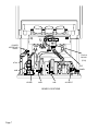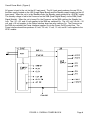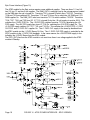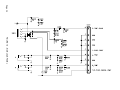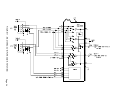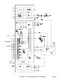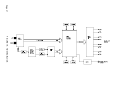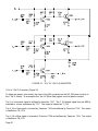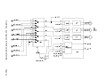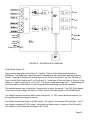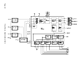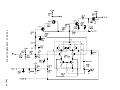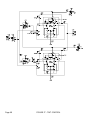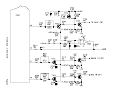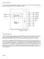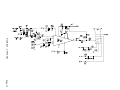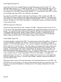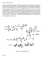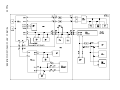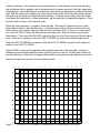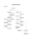
1
PHILIPS
PHILIPS SERVICE AND QUALITY
DPTV400 SERIES
HD PTV
TRAINING MANUAL
TECH
FORCE TRAIN
MANUALS
TRAINING
P H I L I P S
PHILIPS TECHNICAL TRAINING/QUALITY
ONE PHILIPS DRIVE
PO BOX 14810
KNOXVILLE, TN 37914-1810
PHONE: 865-521-4397
FAX: 865-521-4818
EMAIL: [email protected]
Table of Contents
Introduction
Set Operation Highlights................................................................................................................2
Picture formats ..............................................................................................................................3
Native format............................................................................................................................3
4x3 format ................................................................................................................................3
Panoramic format.....................................................................................................................3
Zoom feature............................................................................................................................3
Tuning the ATSC channels ............................................................................................................4
Overall Power Block ......................................................................................................................8
AC Input.........................................................................................................................................9
Standby Power Supply ..................................................................................................................9
Main Power Supply .......................................................................................................................10
Power Fail detection circuit ...........................................................................................................13
ATSC Power Interface for HD version...........................................................................................14
Epic Power Interface .....................................................................................................................15
Horizontal Output circuit ...............................................................................................................16
High Voltage and Dynamic drive ...................................................................................................16
Vertical Amplifier ............................................................................................................................16
Sweep Failure detection and Blanking..........................................................................................20
Video Signal Flow block ................................................................................................................21
Side Jack Panel ............................................................................................................................21
NTSC AV inputs and switching......................................................................................................21
NTSC SSB Processing .................................................................................................................25
ATSC block diagram - HD Version ................................................................................................25
ATSC Block diagram - Epic version ..............................................................................................25
HD-DW module signal flow ..........................................................................................................30
YUV to Y Pb Pr Converter ............................................................................................................31
AV3 and AV4 Inputs and Switching ...............................................................................................33
Scaler Block...................................................................................................................................34
SSM video drive ............................................................................................................................36
Sharpness Control ........................................................................................................................37
Tint Control ....................................................................................................................................37
CRT drive.......................................................................................................................................37
HOP IO ..........................................................................................................................................41
CRT panel......................................................................................................................................41
Audio Signal flow ...........................................................................................................................43
SSB Sound processor ...................................................................................................................43
Audio Amplifier...............................................................................................................................43
Shutdown Mute..............................................................................................................................47
Convergence processor ................................................................................................................48
Intellisense Convergence correction ............................................................................................48
Intellisense Sensing Circuit ...........................................................................................................48
Convergence Horizontal Output ...................................................................................................51
Convergence Vertical Output ........................................................................................................51
Set Control and I2C Busses ..........................................................................................................54
OSD Signal Path ...........................................................................................................................54
Troubleshooting .............................................................................................................................57
Picture problems............................................................................................................................57
Audio Problems .............................................................................................................................58
Service Modes...............................................................................................................................61
Customer Service Mode ...........................................................................................................61
Service Default Mode ....................................................................................................................62
Service Alignment Mode (SAM) ...............................................................................................62
Manual Alignment of the HD_DW module.....................................................................................63
Equipment required .......................................................................................................................64
Offset Adjustments ........................................................................................................................64
Gain Adjustments ..........................................................................................................................64
Gray Scale Alignment ....................................................................................................................65
Error Codes...............................................................................................................................66
Convergence Mode .......................................................................................................................69
Touch Up Convergence...............................................................................................................70
Green Geometry..........................................................................................................................70
Glossary of Terms..........................................................................................................................72
Introduction
The IHDTV2K4 is designed to be marketed in the 2004 model year. This set has a fully integrated
ATSC/NTSC tuning system. This set will tune all of the channels in the NTSC, ATSC, and Cable
bands. There are two RF inputs that are for Cable and Antenna.
The set comes in three versions: the HD, Epic, and Epic Plus. The HD version has the ATSC/NTSC
tuning system. The Epic and Epic Plus versions have two added 1394 inputs. The Epic Plus version also has a Center Channel Amplifier switch which allows the set's speakers to connect to an
external amplifier.
HD Series
Model
51PP9910/17
55PP9910/17
Chassis
DPTV410
DPTV410
Epic Series
51PP9920/17
55PP9920/17
60PP9920/17
DPTV415
DPTV415
DPTV415
It also has NTSC composite and SVHS inputs on AV1 and AV2. AV3 and AV4 can accept
Component signals for either 1Fh (NTSC), 2Fh (480p), 720p, or 1080i. AV3 can be either
Component signal or RGB with separate Horizontal and Vertical sync. AV5 is a HDMI digital video
input. Regardless of the input, the signal to be displayed is converted to 1080i.
Analog Left and Right audio is available on the Output monitor line. This can be either fixed or
variable as selected by the user. Coax digital audio output is available on the S/PDIF OUT line.
The Customer can select either Dolby or PCM output. The set has a 20-watt stereo amplifier.
A ComPair port is available to aid the Technician in troubleshooting the set. The ComPair box and
program are required to communicate with the set.
Page 1
REAR VIEW - HD VERSION
Set Operation Highlights
Figure 1 shows an outline of the Customer menus. Listed below are some of the differences from
previous Philips Projection sets.
In the Picture menu selection, there are the normal controls, Brightness, etc. The COLOR TEMP
selection shifts the color balance of the picture when selected by the Customer. The Warm setting
shifts the white balance to the Red. The Cool setting shifts the white balance of the picture to the
Blue. In the Normal setting, the color temperature of the picture shows the picture with the correct
colors. When a gray scale or black and white picture is shown, there will be no color tint in the picture.
The INTELLITUNE selection under Features will auto-program the channels to add any new channels that may be detected while the set is turned Off. This feature can be switched On or Off by the
Customer. It will not delete any existing channels. The Channel Edit selection under Install is used
to manually install the NTSC channels that are not detected by the AUTOPROGRAM. The WEAK
DIG SIG selection is used to add any digital channels that were not detected by the AUTOPROGRAM selection. To delete all of the channels, use the FACT CH RESET selection (channels are
not deleted when the AUTOPROGRAM selection is made).
In the ATSC system, Emergency alerts can be transmitted as low level or high level. The EMERG
ALERT selection in the menu allows the Customer to turn the low level or high level alert feature On
or Off.
FIGURE 1 - CUSTOMER MENUS
Page 2
Picture formats
Unlike previous sets, the Picture format can be changed without regard to the input.
Native format
The Native format fills the set’s 16 x 9 screen. If
the source picture is in the 4 x 3 format, the set
will stretch the picture to fill the 16 x 9 screen.
4 x 3 format
The 4 x 3 format displays the picture in 4 x3 with
black bars on each side. The bars slowly shift to
prevent CRT burn in.
Panoramic format
The Panoramic format keeps the picture center
linear while stretching the outside edges of the
picture. This allows a 4 x 3 picture to be displayed on a 16 x 9 screen with minimum linear
distortion.
Zoom Format
The Zoom format expands the picture vertically
and Horizontally. This mode is used when the
original picture is in the letterbox format (black
bars on the top and bottom).
Page 3
Tuning the ATSC channels
When the Autoprogram is selected (see Figure 1), both the ATSC and
NTSC channels are tuned.
When the Info button is pressed on the Remote, an information box
will appear as show below. The channel number is shown in the left
part of the box. In the center of the box, the type of channel is displayed. If the channel is an ATSC channel, it will display HDTV. If the
channel is a High Definition channel, it will display SDTV if the channel
is a Standard
Definition channel.
If the channel is an
ATSC channel, the
channel’s call letters and program
list will be displayed if the channel is broadcasting
that information.
The channel number indicated in the
display may not be
the actual frequency being received. In the lower part of the box, signal level is indicated. If the bar is all red, there is not enough signal
detected to properly display the channel. When the red bar ends, a
yellow bar will show. This indicates that enough signal is present to
display the channel, but that it is weak. If a strong signal is present, a
green bar will appear to the right of the red/yellow bar. This indicates
that there is enough signal present to display the signal without problems. If the channel is NTSC, the signal level bar and schedule information will not appear.
Weak Digital Channels can be added to deleted from the program list when the Weak Digital Signal
selection is made in the
main menu (see Figure 1).
Use the cursor up/down
button on the Remote to
select the channels. If a
channel is present, the signal level will be indicated.
If the signal is strong
enough, a picture will be
displayed. Use the cursor
right/left buttons to add or
delete the channel. These
menus are generated by
the ATSC module.
Page 4
Figure 2 shows the Jack Panel for the HD version. AV1 and AV2 inputs and the Side Jack panel
(not shown) are for the NTSC 1Fh input only. AV3 can accept Component or RGB 1Fh, 480p, 720p,
or 1080i inputs. AV4 can accept Component 1Fh, 480p, 720p, or 1080i inputs. AV5 is a HDMI digital input. This can accept 480p, 720p, or 1080i digital signals.
There are two Antenna inputs, Cable and Antenna. Terrestrial ATSC broadcast signals should be
connected to the Antenna input. This input will decode the 8 VSB signals from ATSC broadcast
stations. The Cable input is designed to decode the QAM signals broadcast by the Cable
companies. Either input will receive NTSC broadcast. If the Cable is connected to the Antenna
input, the set will not receive the QAM HD signals transmitted over the cable. The 8 VSB signal is
an amplitude modulated signal with eight levels representating data bit values. The QAM
(Quadrature Amplitude Modulation) signal combines both amplitude and phase modulation. During
Autoprograming, the set will scan both inputs for signals.
Figure 3 shows the Jack Panel for the Epic version. The inputs are the same as the HD version
except for two additional inputs, AV6 and AV7. These inputs are 1394
Firewire inputs. A digital camera with the 1394 output can be connected to these inputs. A Cable card interface will provide the same function
for interfacing with the cable provider as the Set top box. Optical and
Coax Digital audio output is also available. This is only available for the
ATSC channels.
Page 5
FIGURE 2 - HD REAR JACK PANEL
7
FIGURE 3 - EPIC REAR JACK PANEL
Page 6
POWER
INTERFACE
PANEL
FOCUS
BLOCK
(FG2)
ATSC
CRT
PANEL
SSB
HD-DW
SSM
LSB
BOARD LOCATIONS
Page 7
AC INPUT
Overall Power Block (Figure 4)
AC power is input to the set via the AC Input panel. The AC Input panel produces the raw DC for
the Main supply located on the LSB (Large Signal Board) and the Standby supply located on the AC
Input panel. When the set is in the Standby mode, the Standby supply produces a +5VSTBY supply.
The standby voltage is fed to the Processor on the SSB (Small Signal Board) via the SSM (Small
Signal Module). When the set is turned On, the Processor on the SSB switches the Standby line
Low. The +15, +5.2, and +9 volt supplies to the SSM are switched On. The +5.2 volt, 3.5-volt, +15
volt, and +4.5-volt supplies to the Power Interface board are also switches On. The Processor on
the SSB also switches the Power Interface supplies On via the Power On/Off control line. The
Power interface board then produces 3.3 volt, 2.5 volt, 12 volt, 1.2 volt, and 5.2 volt supplies to the
ATSC module.
FIGURE 4 - OVERALL POWER BLOCK
Page 8
AC Input (Figure 5)
AC power is applied to the to the AC Input panel via connector 1206. A series of spark gaps and
capacitors protect the set from damage due to excessive voltage spikes on the AC line. Filter choke
5000 prevents switch mode noise generated by the set from entering the AC power system, causing
interference with other electrical devices. Bridge 6000 produces RAW DC for the Main power supply located on the LSB. Bridge 6001 produces RAW DC for the Standby supply located on the AC
input panel.
FIGURE 5 - AC INPUT
Standby Power Supply (Figure 6)
The Standby supply is located on the AC Input panel. The Standby Supply provides the 5-volt
Standby voltage to the set in the Standby mode. When the set is turned On, it provides +15, +9,
+3.5, +4.5 and +5.2-volt supplies.
Standby B+ is applied to the Standby Switching regulator, 7218 via Pins 6 and 4 of 5202. An internal switch in 7218 charges capacitor 2283 connected to Pin 1 of the IC. When the charge on 2283
reaches 5.8 volts, the internal switch switches to internal. The IC is now being powered by the
charge on capacitor 2283. The internal FET drives transformer 5202 until the charge on capacitor
2283 reaches 4.8 volts. The IC repeats the cycle until the 5-volt Standby voltage reaches the correct level. Shunt regulator 7212 then turns On, turning opto-isolator 7213 On. The operating voltage for 7218 is then supplied by the rectified Hot secondary voltage from Pin 1 of 5202. The internal regulator keeps Pin 1 at 5.8 volts. Regulation is accomplished by monitoring the 5-volt standby
voltage. If the 5-volt supply increases, shunt regulator 7212 will conduct more, causing the resistance of the transistor inside 7218 to decrease. The sensing resistor, Re, inside 7218 will sense the
increase in current and reduce the On time of the internal FET, which will lower the 5-volt supply to
the correct level.
In Standby, the +5 volt, +4.5 volt, and 3.5-volt supplies are being applied to the set. The 3.5 and
4.5-volt supplies are switched on the Power Interface panel. The Standby 5-volt supply is applied to
the Processor located on the SSB. The +15, +9, and +5.2-volt sources are turned Off. When the
set is turned On, the Standby Line goes Low, turning transistor 7214 Off, turning 7205 On, which
turns 7215 On. This switches the +15-volt supply to the set. The +15-volt supply then switches
Page 9
transistors 7216 and 7220 On to switch the +9-volt and +5.2-volt supplies to the set.
When troubleshooting, check for the presence of the operating voltage on Pin 7 of 7218. This is
approximately 160 volts DC. If the Feedback circuit is not working or the secondary is overloaded,
Pin 7 will be pulsing. In this case, check the voltage on Pin 5 of 7213. This is the operating voltage
for Pin 1 of 7218. Each time the 5VSTBY voltage reaches 5 volts, 7212 should turn On. The feedback opto-isolator, 7213 can be checked by applying 5 volts to the +5VSTBY line with AC power
removed from the set. Vary the 5- volt supply between 4 and 6 volts while checking the resistance
between Pins 4 and 5 of 7213. An alternate method of checking this circuit would be to check the
DC voltage on Pins 1 and 2 of 7213. The voltage between these two pins should be 0.7 volts. If
this voltage is present, check Pin 4 of 7213 for a changing voltage. An increase in voltage on this
pin would indicate that 7213 is switching. If the feedback circuit is working, check for an excessive
load on the secondary. If there were no excessive load on the secondary, the cause would be
Capacitor 2283 or IC 7218.
Main Power Supply (Figure 7)
The Full Power supply is located on the Large Signal panel. The Raw B+ voltage from the AC Input
panel is applied to the Full Power switching transistor, 7301 via Pins 6 and 8 of transformer 5300.
This voltage is protected by Fuse 1300 and filtered by Choke 5330. The Standby line goes Low
when the set is turned On. Transistor 7309 is turned Off, which turns 7300 On. This turns Relay
1305 On. Startup voltage is applied to Capacitor 2303 via resistor 3300. When 2303 charges to
14.5 volts, the undervoltage lockout of 7302, connected to Pin 1, is turned On. Drive is output Pin 3
to the Switching FET 7301. This drives 5300 to produce the Full power supply voltages. IC 7302
will continue to drive 5300 until the charges on capacitor 2303 drop below 9.4 volts. The Under
Voltage Lockout of 7302 will then turn the output on Pin 3 Off until 2303 again charges to 14.5 volts.
After several startup cycles, the operating voltage for 7302 is supplied by Pin 10 of 5300.
Regulation is accomplished by monitoring the 130VS supply via resistors 3324, 3350, 3323, and
3322. The Feedback voltage is applied to the Shunt Regulator, 7304, which drives the Feedback
opto-isolator, 7303. The Feedback voltage is applied to Pin 14 of 7302. The voltage is fed to comparator "C" which is referenced to 2.5 volts. This output of this comparator sets the reference voltage for comparator "B" which is compared with the voltage on the source of 7301. This voltage is
developed when 7301 turns On, causing current to flow through resistors 3308 and 3309. If 7301
fails, Resistors 3308 and 3309 should be replaced.
The Full Power supply produces two 130-volt, a 35-volt, a 22-volt, a minus 22-volt, a minus 35-volt,
a plus audio supply, and a minus audio supply. The plus and minus 35-volt, plus 22-volt supplies
power the Convergence circuits located on the SSM. The Audio supply is a plus and minus 19 volts.
This supplies the digital audio amplifier located on the SSM (Small Signal Module).
When troubleshooting, notice that the Hot ground for the Full power supply is separated from the main
Hot ground on the Input Panel by Choke 5330. To ensure correct readings, use the Hot ground in the
Full power supply. If the power supply is overloaded or the operating voltage is missing, the voltage on
Pin 1 of the IC will be changing between 9.4 and 14.5 volts. Each time the voltage reaches 14.5 volts,
drive will appear on Pin 3 of the IC. If the voltage on Pin 1 is rising to 14.5 volts, and drive does not
appear on Pin 3, the IC should be replaced. If a voltage is present on Pin 1 that is greater than 14.5 volts,
and there is no drive on Pin 3, the IC should be replaced. If drive is present on Pin 3, check for drive on
the Drain of 7301. If drive is present here, check for a short on the 130-volt lines, a problem in the feedback circuit, or a problem with the operating voltage.
Page 10
Page 11
FIGURE 6 - STANDBY POWER SUPPLY
FIGURE 7 - MAIN POWER SUPPLY
Page 12
Power Fail detection circuit (Figure 8)
To prevent software problems in the set, the Power Fail detection signals the Processor on the SSB
to place the set in a shutdown state if power is removed while the set is turned On. In addition, the
CRT drive is blanked to prevent phosphor damage to the CRTs.
Voltage from Pin 18 of 5300 is rectified by 6318 and applied to the input of Shunt Regulator 7305.
As long as the voltage to the input of 7305 remains above 2.5 volts, it is turned On. This keeps the
Power Fail and Protect lines Low. If Power is removed from the set, the voltage to the input of 7305
will discharge quickly because of the low capacitance on the input. Shunt Regulator 7305 will then
turn Off. The 130VS supply will then be applied to the Power Fail and Protect lines via resistor
3359. The Power Fail line goes High, signaling the Processor that the set is losing power. When
the Protect line goes High, the CRTs will be blanked and the High Voltage will be turned Off.
FIGURE 8 - POWER FAIL DETECTION CIRCUIT
Page 13
ATSC Power Interface for HD version (Figure 9)
The ATSC Power Interface module produces the operating voltages for the ATSC module. The +15,
3.5, 4.5, and 5.2-volt supplies from the AC Input panel are fed to the Interface module. The
Processor on the SSB provides a On/Off command to switch the outputs. In the Standby mode, the
On/Off line is High. This switches transistor 7202 On, which turns transistors 7206, 7204, and 7205
On. This turns the Regulators 7101, 7102, 7103, 7105, and 7104 Off. When the set is turned On,
the On/Off line goes Low, switching 7202 Off which turns 7206, 7204, and 7205 Off. This turns
Regulators 7101, 7102, 7103, 7105, and 7104 On. The output of 7101 turns transistors 7203 On to
switch the 5.2-volt supply to the ATSC module. A 12-volt, 5.2-volt, two 1.2-volt, 2.5-volt, and 3.3-volt
supplies are fed to the ATSC module. Sense line from the ATSC module for the two 1.2-volt and the
2.5-volt supplies provides precise regulation for those supplies.
FIGURE 9 - ATSC POWER INTERFACE - HD VERSION
Page 14
Epic Power Interface (Figure 10)
The ATSC module for the Epic version requires some additional supplies. There are three 1.2, two 3.3,
two 2.5, two 12, and two 5-volt supplies. The DAM_CNTL is switched Low by the microprocessor located
on the SSB when the set is turned On. Transistor 7201 is turned Off which turns 7202 Off. Transistors
7208 and 7203 are switched Off. Transistors 7212 and 7214 turn On to switch the +5V DAM and +12V
DAM supplies On. The DAM_CNTL also turns transistor 7211 On which switches 7209 Off. Transistors
7206, 7207, 7204, and 7205 turn Off. IC 7101 is turned On by the +15-volt supply via resistor 3204. This
switches the +12VDC POD On. The +12VDC POD switches transistor 7213 On, developing the +5V
POD supply. The +5V POD supply then turns IC 7105 On, switching the +3.3V POD supply On. The
+3.3V POD supply switches ICs 7107, 7103, and 7102 On. This switches the +2.5VDC POD, +1.2VDC
CH2 POD, and +1.2VDC CH1 supplies On. The +1.2VDC CH1 supply is fine tuned by feedback from
the ATSC module via the +1.2VDC Sense Ch1 line. The +1.2VDC CH2 POD supply is controlled by the
ATSC module via the +1.2VDC Ch2 feedback. In the same manner, the +2.5VDC DAM supply is controlled by the +2.5VDC Sense from the ATSC module.
The POD_CNTL line from the ATSC module is not used since there is no voltage applied to the ATSC
module in Standby.
Page 15
FIGURE 10 - ATSC POWER INTERFACE - EPIC VERSION
Horizontal Output circuit (Figure 11)
Horizontal drive from the HOP circuit on the SSM is fed to 7807 on the Large Signal panel.
Transistor 7807 drives the Horizontal Output Transistor 7801, which drives the Yokes and the
Horizontal Output Transformer 5801. Transformer 5801 produces a plus and minus 13-volt supply
for the Vertical Output circuit. Voltage from Pin 7 of 5801 is rectified by 6802 to produce the +200volt supply for the CRTs. Voltage from Pin 5 is rectified by 6801 to produce the Filament voltage.
This voltage is filtered by 2804 to provide approximately 6 volts DC. This circuit is protected by fuse
1801 and resistor 3801. The negative Horizontal pulse from Pin 5 feeds the Blanking and Sweep
failure detection circuit.
The output of 7807 drives IC 7803 and transistor 7802. This circuit drives the Dynamic Focus and
Horizontal Geometry correction. The Horizontal component of the correction drives the return side
of the Horizontal yokes via the DYN-FOCUS-HIGH and DYN-FOCUS-LOW lines.
High Voltage and Dynamic drive (Figure 12)
The High Voltage module is an integrated High Voltage supply with its own switching power supply.
When the set is turned On, approximately 10 to 11 volts from the Sweep Failure detection circuit is
fed to diode 6913 and to Pin 8 of the High Voltage module. A supply voltage of 130 volts is also fed
to Pin 10 of the module. The Module then outputs High voltage to the three CRTs. It also outputs
Focus voltage to the Focus G2 block. Output on Pin 4 is rectified by 6917 to produce a negative
200-volt source for the CRT G1 voltage. The voltage is also rectified by 6919 to produce a 330-volt
source for the Dynamic Focus drive. The Dag line along with the output on Pin 2 is connected to
7903 to produce the ABL voltage for the set. If an overcurrent condition should develop with the
drive, the ABL voltage will go Low, turning 7905 On, latching 7904, which will remove drive to Pin 8
of the HVG. This will cause the High voltage to shut Off. The DM-INPUT is mixed with the East
West drive EWO and fed to transistor 7903 which drives 7901. Transistor 7901 drives the Dynamic
Focus and geometry correction drive which is fed to the return side of the Horizontal Yokes via the
DYN-FOCUS-LOW and DYN-FOCUS-HIGH connections.
Vertical Amplifier (Figure 13)
The Vertical drive from the HOP panel drives the Vertical Output IC 7811. This IC is located on the
Large Signal panel. Drive is fed to Pin 7 and is output on Pin 5 to drive the three Vertical Yokes.
This IC is powered by the plus and minus 13-volt supplies from the Horizontal Output circuit. A
Vertical pulse on Pin 6 is fed to the sweep failure detection circuit. If there is a failure in the
Horizontal or Vertical sweep, the High Voltage will be shut down.
Page 16
Page 17
FIGURE 11 - HORIZONTAL OUTPUT
FIGURE 12 - HIGH VOLTAGE
Page 18
Page 19
FIGURE 13 - VERTICAL AMPLIFIER
Sweep Failure detection and Blanking (Figure 14)
The Shutdown circuit will shut the High voltage Off if the Horizontal or Vertical Sweep should fail. It will
also shut the High voltage Off if the Power Fail line goes High or the +200-volt source should fail.
The Vertical pulse is fed to zener diodes 6824 and 6814, which keep capacitor 2837 charged. This
pulse is rectified by 6815 to keep the base of 7808 at a negative voltage. This keeps the transistor
turned Off. In the same manner, the Negative Horizontal pulses keep the base of 7810 at a negative voltage to keep it turned Off. The Protect line is normally Low, keeping 7809 turned Off. The
+200-volt source is fed through zener diodes 6812 and 6816, resistor 3850, the base-emitter of
7906, the base emitter of 7812 to keep transistor 7813 turned On. This turns transistor 7814 On,
which switches the On voltage to the High Voltage module. The conduction of 7812 keeps the voltage on the G1 line at approximately -18 volts, which turns the CRTs On. If the Vertical Pulse should
fail, transistor 7808 will turn On, which will turn 7906, 7812, 7813, and 7814 Off. This will turn the
HVG module Off. In addition, when 7812 turns Off, the G1 voltage will go to -200 volts, blanking the
CRTs. The same sequence will occur if Horizontal should fail. The Protect line should go High, or
the +200-volt source should fail.
FIGURE 14 - SWEEP FAILURE DETECTION AND BLANKING
Page 20
Video Signal Flow block (Figure 15)
The Tuning system will tune all of the channels in the ATSC, NTSC, and Cable bands. Whichever
channel is selected by the Customer, the video signal is converted to a Digital 8-bit TMDS signal.
This signal is fed to the Scaler IC on the HD/DW panel. Composite or SVHS NTSC signals are fed
to the set via the Side Jack panel, AV1, or AV2. These signals are fed to a Switch located on the
SSM (Small Signal Module). The selected Composite or YC signal is then fed to the HIP circuit on
the SSB where it is changed to a YUV signal. The YUV signal is fed to the HD/DW module for digital processing. The AV3 and AV4 Component signals are fed directly to the HD/DW module. Digital
480p, 720p, or 1080i is fed to the HD/DW module via the HDMI input. The Scaler on the HD/DW
module resizes the picture to 1080i. The 1080i signal is then output to the SSM to the HOP and
CRT drive circuits. OSD (On-Screen Display) generated by the Processor on the SSB is fed to the
HOP to be inserted into the CRT RGB signals. Horizontal and Vertical from the HOP is fed to the
LSB (Large Signal Board) to drive the Scan circuits.
Side Jack Panel (Figure 16)
The Side Jack panel has a Composite Video and SVHS input. When there is a connector in the SVHS
input, the Composite input is muted. Resistors 3001, 3002, and 3000 on the Video, Y, and C lines provide 75-ohm impedance matching. If a cable is plugged into the SVHS connector, the line connecting
resistor 3029 to ground is removed causing the voltage on the Y/C_CVBS_SENSE_FRNT line to
increase. This signals the Microprocessor to switch the video switching circuits from composite video to
YC in.
NTSC AV inputs and switching (Figure 17)
AV1 and AV2 Composite and SVHS inputs are located on the SSM. These inputs as well as the
Side Jack panel are fed to the Video Switch, 7017. This IC is controlled by the Processor on the
SSB via the SCL_IN and SDA_IN bus. Composite video or Luminance is output on Pin 1 and
buffered by 7003 before being fed to the SSB. The Chroma signal is output on Pin 3 and buffered
by 7102. If a SVHS signal is connected to one of the AV inputs, the S-1, S-2, or S-3 lines will go
Low for that respective input. The Processor will read these Pins via the I2C bus and signal the HIP
that the signal present is YC instead of Composite.
Page 21
FIGURE 15 - VIDEO SIGNAL FLOW BLOCK
Page 22
Page 23
FIGURE 16 - SIDE JACK PANEL
FIGURE 17 - SSM NTSC AV INPUTS AND SWITCHING
Page 24
NTSC SSB Processing (Figure 18)
Composite video or YC from the SSM is fed to the HIP, 7323, located on the SSB. The Composite
or Y signal is input on Pin 20 and the Chrominance or C is input on Pin 21. If the input is a YC,
SVHS signal, the Y is fed to the Delay and the C is fed to the Demodulator. If the input is a
Composite signal, it is output on Pin 26 and buffered by 7320 before being fed to the Comb filter, IC
7307. The Y is then fed back to 7323 on Pin 28 and the C on Pin 29. The YUV from the Delay and
Demodulator is fed to an internal switch and output on Pins 49, 50, and 51. The YUV is then fed to
the HD/DW module via the SSM.
ATSC block diagram - HD Version (Figure 19)
Due to the difficulty in changing some of the components on the ATSC module, it is to be changed
as a module only.
The Tuner, U501, can tune both NTSC and ATSC channels. If the selected signal is NTSC,
Composite video is output from the tuner to a 3D Comb filter. YC is then fed to U503, Analog to
Digital converter. The signal is then fed to U201, Digital Decoder. If the signal is ATSC, the 8-bit
compressed data stream is detected and sent to the Digital Decoder. The Digital Decoder decompresses the MPEG-2 ATSC signal. The signal is then fed to a TMDS transmitter before being sent
to the HD-DW module. The Digital Decoder outputs a digital audio signal when an ATSC channel is
selected. This signal is output on a Coax Digital audio output.
ATSC Block diagram - Epic version (Figure 20)
The Epic version has all of the functions of the HD version with the addition of two 1394 firewire
inputs and a POD jack. The 1394 inputs can be used for digital cameras, set-top boxes, and other
devices with that output format. The POD has a receptacle which allows a card supplied by the
cable company to be inserted. It allows for the reception of Pay channels in the same manner as
the set top box supplied by the cable company. The output of the ATSC Tuner is fed to U1300
which detects the cable company control data from the signal and communicates with the POD.
The 8-bit ATSC signal is then fed to the Digital Decoder as before. All other signal processing is
performed in the same manner as the HD version. There is also a Digital Coax and Optical output
for ATSC digitally encoded audio.
Page 25
FIGURE 18 - NTSC SSB SIGNAL PROCESSING
Page 26
Page 27
FIGURE 19 - HD ATSC BLOCK
FIGURE 20 - EPIC ATSC BLOCK
Page 28
Page 29
FIGURE 21 - HD-DW MODULE
HD-DW module signal flow (Figure 21)
The AV3 and AV4 inputs located on the HD-DW module are fed to 7100 for selection. The selected
Y Pb Pr or RGB signal is fed to an A/D converter, 7400. The YUV signal from the SSB is fed to a
YUV to Y Pb Pr converter and then to 7400. IC 7400 selects between the two inputs and converts
them to digital Red, Green, and Blue signals. The HDMI, similar to DVI, is fed to the HDMI receiver.
The output of the HDMI receiver is connected to the same data buses as 7400. These data busses
containing picture data are fed to the Scaler IC, 7601. TMDS Picture data from the ATSC module is
fed to 7500, TMDS Receiver where it is decoded back to three 8-bit data lines. This output is also
fed to the Scaler IC.
The Scaler IC enhances the picture and resizes it to a 1080i. It also performs the PIP function. Any
of the AV inputs or the HDMI input can be the main picture while the ATSC output can be in the PIP
window, or the ATSC can be in the main picture while any of the AV inputs or HDMI input can be in
the PIP window.
The output of the Scaler, which is a 1080i signal, is fed to Switch 7800. IC 7800 always selects the
Scaler in normal operation. The output of 7100 is only selected in certain factory test modes. The
Horizontal frequency of the sync is 33.75kHz while the vertical is 60Hz.
Page 30
FIGURE 22 - YUV TO Y Pb Pr CONVERTER
YUV to Y Pb Pr Converter (Figure 22)
To obtain the proper color match, the input of the A/D converted on the HD_DW panel must be in
the Y Pb Pr format. To accomplish this, the UV (Blue Red) signals must be phase inverted.
The Y or Luminance signal is buffered by transistor 7207. The Y_IN labeled signal from the SSB is
matched to a lower impedance by 7207. The output is labeled as Y_YUV.
The V_IN or Red signal is inverted by Transistor 7203 and buffered by Transistor 7202. The output
is labeled as PR_YUV.
The U_IN or Blue signal is inverted by Transistor 7205 and buffered by Transistor 7204. The output
is labeled as PB_YUV.
Page 31
FIGURE 23 - AV3 AND AV4 INPUTS AND SWITCHING
Page 32
AV3 and AV4 Inputs and Switching (Figure 23)
The input to AV3 can be either in the Y Pb Pr or RGB formats. The sync for the RGB format can be
separate Horizontal and Vertical or Sync on Green. The Component Y Pb Pr connected to AV3 or
AV4 can be a 1 fH (480i), 2 fH (480p), 720p, or 1080i signal. Component Y Pb Pr or RGB can also
be connected to AV4. An RGB signal must have Sync on Green for this input. There are no separate Horizontal and Vertical sync inputs for AV4.
IC 7100 selects Component video or RGB from AV3 or AV4. IC7100 is controlled by the HD_SEL
control line from the HD_DW processor, 7700.
IC 7400 is an A/D (Analog to Digital converter), Sync processor, and Video switch. The IC selects
between the output of 7100 and the Y Pb Pr signals from the YUV to Y Pb Pr converter. The
Clamping circuit sets the sampling point and amplitude of the incoming signal before feeding it to the
A/D converter. The signal sampling Offset and Drive levels are set in the SAM menu which are
explained in the adjustment section. The output of the A/D converters is fed to the Scaler on three
eight bit data lines. These Data lines are shared with those from the HDMI receiver. When the
HDMI receiver is switched On, the data lines are switched Off becoming open circuits.
If the Sync of the applied signal is Sync on Green or Sync on Y, the Y or Green signal on Pin 30 is
fed to the Scaler IC for Sync detection. If separate Horizontal and Vertical Sync is applied to AV3
and AV3 is selected, it is output on Pins 22 and 21. Vertical Sync is fed to Pin 42 of 7400.
Horizontal Sync is fed to 7401-A. If separate Horizontal and Vertical Sync is present, the Processor
on the HD_DW panel will switch the H-RGB_SEL line High, switching the Horizontal Sync to Pin 43
of 7400. The Sync is processed and output on Pins 125 and 127.
IC 7400 is controlled by the SDA_MP and SCL_MP date line from the Microprocessor, 7700, located
on the HD_DW panel.
Page 33
FIGURE 24 - SCALER BLOCK DIAGRAM
Scaler Block (Figure 24)
There are two input ports to the Scaler IC, A and B. The two 24 bit video inputs are fed to a
Multiplexer. The Multiplexer selects the picture information for the main picture and the Picture in
Picture. Separate Horizontal and Vertical Sync for the A-Port is fed to the IC on Pins 156 and 157.
Sync for the B-Port is fed to the IC on Pins 9 and 10. In the case of Sync on Green or Sync on Y, the
Green or Y signal is fed to the IC on Pin 207. The Sync is separated inside the IC. The frequency of
the Horizontal and Vertical Sync is used for signal processing timing and Format detection.
The selected picture data is fed to the Format circuits to resize the picture. The CSC (Color Space
Conversion circuit) changes the data to a YCbCr format if the input signal is in the RGB format.
The Image Processor enhances and Formats the picture. IC 7600 stores the picture data as it is
being processed by the Image Processor.
The Scaler converts the output to a1080i format. The signal is fed to three D/A converters. The IC
then outputs an analog Y Pb Pr output. Horizontal and Vertical sync is output on Pins 49 and 50.
The Vertical is 60 Hz while the Horizontal is 33.75 kHz.
Page 34
Page 35
FIGURE 25 - SSM VIDEO DRIVE
SSM video drive (Figure 25)
The Y/G, B/Pb, and R/Pr signals are fed to their respective sharpness controls. If the input is a YUV
signal, the Y signal is fed to Pin 28 of 7600. The U and V signals are fed to the Tint Control circuit
and then to Pins 27 and 26 of 7600. In this case, this input will always be Y Pb Pr.
The input selector switch in 7600 selects between the YUV on Pins 28, 27, and 26 or the output of
the internal RGB/YUV converter. The signal is fed to the RGB insertion circuits where the OSD is
inserted. The signal is then fed to a White Point circuit and then to the Output Amplifier. The White
Point and Output Amplifier have the Drive controls and Cutoff controls. Input from the ABL line on
Pin 43 makes adjustments in the brightness levels to adjust for changes in beam current. The AKB
pulses from the CRTs are fed to Pin 44 to the Cathode Calibration circuit. The Cathode Calibration
circuit adjusts the cutoff levels of the CRTs to maintain the correct gray scale tracking. When the set
is first turned On, a calibration pulse is output on the RGB lines. The Cathode Calibration circuit
monitors this pulse on the AKB line to set the Black level and the maximum drive voltage for the
cathode. Once the Calibration has taken place, the Output Amplifier switches to the RGB drive signal as the output.
Horizontal and Vertical Sync is fed to 7600 on Pins 23 and 24. IC 7600 processes the sync to provide the geometry for the picture. Horizontal drive is output to the sweep circuit on Pin 8. Vertical
drive is output on Pins 1 and 2. East West drive is output on Pin 3. Sandcastle (SCO) is output on
Pin 9. Horizontal Feedback (HFB) from the sweep circuit is fed into the Phase Loop to phase correct the Horizontal drive.
IC 7600 is controlled by the GDE Microprocessor on the SSM via the I2C buss on Pins 10 and 11.
Geometry and Drive settings are stored in the Memory IC located on the SSM.
Page 36
Sharpness Control (Figure 26)
The Sharpness controls for the YUV/RGB signals are located on the SSM. Since all three circuits
are basically the same, only the Blue one will be discussed.
The Blue signal is fed to Pin 1 of 7410. It is also fed to a Low Pass filter consisting of 5411 and
5410. This path is amplified by transistor 7411. The Low Pass filter blocks the Higher frequencies
as well as shifting the phase of the signal. The output of the Low Pass filter is also fed to Pin 4 of
7410. The mixing of these two phase shifted signals only allows the High frequency component to
be amplified and output on Pin 12. The gain of the High frequency component is controlled by the
Sharpness voltage, which is applied to Pins 8 and 10. The two signals are combined at Pin 12 of
the IC. If the input was a Blue signal it is amplified by 7412 and buffered by 7413. If the input was
a U signal, it is buffered by 7414.
Tint Control (Figure 27)
IC 7510 amplifies the U signal while 7520 amplifies the V signal. The Tint control voltage changes
the balance between the U (Pb) and V (Pr) signals to change causing the tint of the picture to
change.
CRT drive (Figure 28)
The output of 7600 is fed to the RGB amplifiers before being fed to the CRTs. Transistors 7720 and
7721 buffer the Blue output on Pin 42. The B-BIAS control voltage controls the gain of this circuit.
Transistor 7730 provides an additional voltage gain for the signal.
7710 and 7711 buffer the Green output from Pin 41 of 7600. The G-BIAS controls the gain of the
circuit.
The Red output from Pin 40 of 7600 is buffered by 7700 and 7701. The R-BIAS controls the gain of
the circuit.
The drive of the Red and Green outputs is compared with the Blue drive by 7900-A. The difference
signal is fed back to 7600 via the ABL line. If the Blue CRT is driven harder than the Green and
Red CRTs, the inverting input on Pin 2 will become greater than the non-inverting input on Pin 3,
resulting in the output on Pin 1 to go Low. The ABL line will go Low, causing 7600 to reduce the
drive to all of the CRTs. This circuit prevents the Blue tube from being over-driven.
Page 37
FIGURE 26 - SHARPNESS CONTROL
Page 38
Page 39
FIGURE 27 - TINT CONTROL
FIGURE 28 - CRT DRIVE
Page 40
HOP IO (Figure 29)
IC 7800 develops the analog control voltage for the HOP circuit. The I2C bus from the GDE microprocessor controls the IC. This IC is located on the SSM.
FIGURE 29 - HOP I/O
CRT panel (Figure 30)
The Red, Green, and Blue signals from the HOP panel are fed to their respective CRT panel. The
signal is fed to the emitter of 7200 and then to 7202. The output of 7202 is fed to Pin 2 of 7201
which drives the cathode of the CRT. AKB drive is output on Pin 7 and fed to the HOP panel.
The CRT circuit is powered by the +200-volt supply from the LSB. If there is a problem in this circuit, the one resistor, 3217, will open. If this resistor opens, the CRT will have excessive drive causing it to go to maximum brightness. This will cause an over current shutdown on the LSB. In normal operation, the G1 voltage will measure approximately minus 20 volts. During blanking, this voltage will go to a minus 200 volts. The Filament voltage will measure approximately 6 volts DC. If
drive is removed to any of the CRT boards, the CRT will be driving into saturation, causing an over
current shutdown.
Page 41
FIGURE 30 - CRT PANEL
Page 42
Audio Signal flow (Figure 31)
Audio inputs for AV3, AV4, and AV5 located on the HD-DW module are fed to Switch 7101. The
selected outputs are fed to 7017, located on the SSM. IC 7017 selects between the output of 7101,
AV1, AV2, and the Side Jack panel. The selected output of 7017 is fed to the ATSC module. The
Sound Processor on the ATSC module selects between 7017, Tuner Sound IF when NTSC is selected, and Digital audio when ATSC or the 1394 inputs are selected.
The output from the ATSC module is fed to the Sound Processor, 7561, located on the SSB. IC
7561 controls the volume, balance, base, treble, and enhanced sound functions. The output of the
Sound Processor, 7561, is fed back to the SSM to the Audio Amplifier, 7700. For the HD and Epic
versions, the output of 7700 is fed to the speakers. In the Epic plus version, the output is fed to the
Center Channel switch.
SSB Sound processor (Figure 32)
Audio processing is performed by 7651, located on the SSB. Selected AV audio is fed to Pins 42,
41, 45, and 44. The Demodulator detects and decodes the signal before feeding it to the processing
section. The selected AV audio is fed to two A/D converters and then to the processing section.
The Sound processing includes Volume, Equalizer, Balance, Loudness, Incredible Sound, and
Virtual Dolby. After processing, the Audio signal is fed to six D/A converters. The Main Speaker
Audio is output on Pins 20 and 21. AV out Audio is output on Pins 25 and 26.
Audio Amplifier (Figure 33)
The Audio Amplifier is located On the SSM. The output power for the Audio Amplifier is 10 watts per
channel for the Basic and Basic Plus versions. The Core Version has an output of 15 watts per
channel. IC 7700 is the Audio output IC. This is a class D amplifier. Left and Right Audio from the
SSB is fed to Pins 10 and 18 of the IC. The output stages are basically switch mode circuits driven
by the audio input signal. The frequency of the output is kept at 200 kHz by an internal 200 kHz
oscillator. The pulse width of the output is determined by the signal level of the input signal. The
Right Channel pulse width signal is output on Pin 3. The output is filtered by 5701, 2777, 2776,
2717, 5716, and 2737. The amplified audio is output on connection 1349. In the same manner, Left
audio is output on Pin 23. The IC is powered by +19 and -19 volt supplies. The supplies are
protected by fuses 1700 and 1701. The Supply voltage for the Core version is 4 volts higher than
the Basic and Basic plus version. The extra supply voltage is needed to produce the additional 5
watts per channel output.
Muting and volume control for the audio take place in the Audio Signal processor on the SSB. The
STBY MUTE line on Pin 6 goes to 2.5 volts to mute the audio when the set is turned On or Off. This
line goes Low to place the amplifier in a Standby mode if a DC voltage is detected on the Audio
Output lines.
Page 43
FIGURE 31 - AUDIO SIGNAL FLOW BLOCK
Page 44
Page 45
FIGURE 32 - SSB AUDIO PROCESSING
FIGURE 33 - AUDIO AMPLIFIER
Page 46
Shutdown Mute (Figure 34)
The Audio Amplifier will be placed in a Standby mode and the set will shut down if a DC voltage is
detected on the Speaker Output lines. The Left and Right audio output lines are connected to the
base of 7704 and the emitter of 7705 via resistors 3718 and 3717. Filter capacitor 2778 filters out
the AC component of the waveform. If the DC voltage goes positive, 7704 will turn On. If the voltage goes negative, 7705 will turn On. This turns 7706 On, which turns 7707 On. This causes the
Front Detect line to go Low, preventing the Microprocessor from receiving any commands. It also
turns SCR 6701 On, turning transistor 7708 On, causing the Standby line to go High. If this SCR is
turned On, it will be necessary to remove power from the set to reset the circuit. This will turn the
set Off. Transistor 7707 also turns On, causing the Standby-Mute line to go Low. This places the
Audio Output IC in a Standby mode. If the Power Fail line should go High, 7710 will turn On, causing the Standby-Mute line to go Low.
FIGURE 34 - SHUTDOWN MUTE
Page 47
Convergence processor (Figure 35)
The Convergence data is stored in the EEPROM, 7000. The Microprocessor located on the ASC
module reads 1,971 bytes of data from 7000 and writes it to the Convergence Processor, 7052.
Horizontal sync is inverted by 7069, buffered by 7068, and fed to Pin 27 of 7052. Vertical sync is
inverted by 7070, buffered by 7071, and fed to Pin 28 of 7052. The data is processed to produce
the desired convergence correction waveforms which are output on six DACS. During the convergence adjustment procedure, a 180-point alignment grid is output on Pins 16, 17, and 18. This signal is mixed with the OSD to be displayed on the screen. There is only one convergence mode for
this set, 1080i. The output of the DACS is fed to six op-amps before being fed to the Power
Amplifiers located on the SSM. When screen centering is being performed, it is necessary to disable the convergence drive waveform.
Intellisense Convergence correction (Figure 36)
The Intellisense system is only used in the Epic
version. The Philips Intellisense system makes
minor Convergence corrections when the feature is selected by the Customer. When a PTV
is moved from one location to another, minor
Convergence errors will occur due to changes
in the Earth's magnetic field. When Save is
selected during the Convergence Alignment, the
set scans four optical sensors with each of the
three colors. The locations of these sensors
are recorded by the ACS Microprocessor. When
the Customer selects the Intellisense feature,
the sensors are again scanned and the rotation
of the beams for each color is adjusted to the
recorded values.
FIGURE 36
Intellisense Sensing Circuit (Figure 37)
The output of the four sensing Solar Cells is fed to IC 7141, located on the ACS module. Inputs
TBU0, TBU1, and TBU2 from the Convergence Microprocessor are fed to the Decoder which selects
the Solar Cell to be read. The output on Pin 3 is fed to Pin 2 of 7140-1. 7140-1 matches the low
impedance output of 7141 to the high impedance input of 7140-2. Amplifier 7140-2 charges capacitor 2253 with the sample voltage. Due to the high input impedance of 7140-3, 2253 will hold the
sample voltage until it is cleared by transistor 7540. The output of 7140-C is fed to 7101, an Analog
to Digital converter. The Digital reference voltage is fed to the ACS microprocessor where the data
is processed and recorded. When the next location requires sampling, a High is output on Pin 100
of 7100. This turns Transistor 7541 On, discharging capacitor 2253.
The Basic version of the HDRPTV does not have the Sensors installed in the set. However, the
Sensor Test is in the Service Convergence menu. When the Convergence alignments are stored,
the Microprocessor will attempt to read the Sensors. If the Sensor test is selected in the
Convergence Alignment menu, the message will read "Sensors not verified at locations: 1234." This
will not affect the Convergence alignments.
Page 48
Page 49
FIGURE 35 - CONVERGENCE PROCESSOR
FIGURE 37 - INTELLISENSE SENSING CIRCUIT
Page 50
Convergence Horizontal Output (Figure 38)
IC 7044 amplifies the Horizontal convergence waveforms. The correction waveforms are fed to the
IC on Pins 6, 14, and 15. They are output to the Convergence Yokes on Pins 9, 11, and 18. The IC
is powered by four supply inputs. A +35-volt supply is fed to Pin 5, a -35-volt supply is fed to Pin 4,
and a -22-volt supply is fed to Pin 8, 12, and 17. The supply fed to Pin 10 is normally a +22-volt
supply. During signal peak drives, the voltage on Pin 10 is increased to +35 volts. Feedback sense
voltage is developed across the 6.8 ohm resistors on the return side of each yoke. Transistor 7007
is part of a Soft Start circuit. When the set is turned On, Transistor 7007 turns On until capacitor
2043 is fully charged. While 7007 is being turned On, a negative voltage is placed on Pin 3 muting
the output of the IC. A 100-ohm snubber resistor is across each of the yoke windings. This resistor
will overheat if the unit is operated with the Convergence Yokes unplugged.
Convergence Vertical Output (Figure 39)
IC 7045 amplifies the Vertical convergence waveforms. The correction waveforms are fed to the IC on
Pins 6, 14, and 15. Output is on Pins 9, 11, and 18 to the Vertical Convergence yokes. Feedback
sense voltage is developed across the 6.8-ohm resistors on the return side of each yoke. A Snubber
resistor is across each yoke. These resistors will overheat if the circuit is operated without the
Convergence Yokes being plugged in. The IC is powered by four supplies: a +35 volt, -35 volt,
VccPSW-V, and VCCNSW-V. The VccPSW-V supply is normally at +22 volts. The BV_OUT,
GV_OUT, and RV_OUT lines are connected to a Vertical Power up circuit which senses the drive to
the Convergence Yokes. If the drive to the yokes reaches 10 to 12 volts, the Vertical Power up circuit
will switch the VccPSW-V supply to +35 volts. If the Vertical Power up circuit senses a negative 10 to
12 volt drive to the Vertical Convergence yokes, the VccNSW-V supply will switch from -22 volts to -35
volts. As with the Horizontal drive circuit, 7005 mutes the output of 7045 during power up.
Page 51
FIGURE 38 - CONVERGENCE HORIZONTAL DRIVE
Page 52
Page 53
FIGURE 39 - VERTICAL CONVERGENCE DRIVE
Set Control and I2C Busses (Figure 40)
Commands to the set by the Consumer are sent via the Keyboard and Remote Control to the
Painter (Microprocessor), 7001, located on the SSB. The Painter sends commands to the ATSC
Digital Decoder on the SDA-S line via the SSM. The Digital Decoder controls the Tuner, Sound
Processor, and other devices on the ATSC module.
The NVM, 7012, on the SSB stores Option Codes, Error Codes, and Customer settings. The SDA-F
line controls the HIP (High end Input Processor) and MSP (Audio Processor) on the SSB. This line
also controls the AV in switch on the SSM and the time Clock. This line is also used to send commands to 7700, HD/DW Processor. The ComPair connector is located on the SSM and is connected to the SDA-F line. The HD/DW processor controls the devices on the HD/DW module.
The RXD and TXD lines on the Painter communicate with the GDE processor located on the SSM.
The GDE processor controls the HOP via the SDA-C line. It communicates with the Convergence
Processor and NVM via the SDA-B line. The NVM on the SSM stores White Tone information,
Geometry settings, and Convergence data. The Standby and DAM_CTL lines control power switching in the set. The Standby switches the Main and Standby supplies. The DAM_CTL line switches
power to the ATSC module.
OSD Signal Path (Figure 41)
On-Screen Displays are generated by the Painter, ATSC Processor, GDE Processor, and
Convergence Processor. When the Menu button is pressed or a channel is entered, the OSD is
generated by the Painter on the SSB. Display related to channel display information, other that initial channel entry, is generated by the ATSC module.
When the set is placed in the SAM (Service Alignment Mode), the SAM menu is generated by the
Painter, 7001. When the GDE sub menu is selected, the display is generated by 7100, GDE
processor.
During the Convergence mode, the menus are generated by the GDE processor. The Convergence
Grid is generated by the Convergence processor.
OSD information from the Convergence Processor, 7052, is buffered by transistors 7059, 7060,
7061, and 7062. OSC information from the GDE and Painter is added. The OSD is then fed to the
HOP, 7600, where it is inserted into the YUV picture information from the HD/DW module.
Page 54
Page 55
FIGURE 40 - SET CONTROL AND I2C BUSSES
FIGURE 41 - OSD SIGNAL PATH
Page 56
Troubleshooting
(Figure 42)
When power is applied to the set via the AC Input panel, the 5-volt standby voltage should be present on Pin 3 of 1203 on the AC Input panel. The RAW DC and Startup voltage should be present
on Pins 5 and 3 of connector 1500. The RAW DC should be approximately 140 to 160 volts DC. If
the RAW DC voltage is missing, check the line for low resistance before changing the repairing or
replacing the AC Input panel. The Startup voltage should be approximately 60 volts. The ground
on Pin 1 of 1500 should be used as the reference when measuring these voltages.
The Standby line on Pin 3 of connector 1203 should read approximately 3.3 volts when the set is in
Standby. This line is controlled by the Painter processor, located on the SSB. When the set is
turned On, the Painter will pull the Standby line Low. This will switch the +15, +5.2, and +9 volt supplies on connector 1203 On. The 3.5 volt, 15 volt, and 4.5 volt lines on connector 1202 are also
switched On. The Power On/Off (DAM_CNTL) line on Pin 1206 of the Power Interface board will
switch Low to switch the voltages from the Power Interface board to the ATSC module. The PODCONTROL line from the ATSC module must also switch Low if the set is an Epic or Epic plus version. The POD-CONTROL line is not used for the HD version.
When the Standby line goes Low, it also turns the Main Power supply located on the LSB On. This
can be checked on Pin 6 of connector 1518 on either the LSB or SSM. The operation of the Main
supply can be checked by measuring the 130-volt supply on Pin 8 of 1518. If the 130-volt supply
comes On, then Off, check the PWR_FAIL line on Pin 10 of 1518. Set the oscilloscope to DC and
monitor this Pin while turning the set On. If this line goes High and the Standby line goes High,
there is a problem with the Power Fail detection circuit on the LSB. The LSB should be repaired or
replaced. In conclusion, if the RAWDC and STARTUP are present on Pin 15, the Standby line on
Pin 6 of 1518 goes Low and stays Low, and the 130 volt should turn On. If it does not turn On, the
LSB should be repaired or replaced.
Picture problems
Picture drive is developed from three different areas. ATSC/NTSC video is fed to the HD/DW module via the TMDS/DVI line. This is serial digital data which can be checked on connector 1504 on
the HD/DW module. 1Fh NTSC video is switched on the SSM before being sent to the SSB for processing. The signal can be checked on Pin 6 of connector 1420 on the SSM. YUV from the SSB is
fed to the HD/DW module via the SSM. The signal can be checked on connector 1200 on the
HD/DW module. Component video, RGB, or HDMI is fed to the HD/DW module via AV3, AV4, or
AV5. The Y Pb Pr signals from the HD-DW module are sent to the SSM via connector 1800 on the
HD-DW module and 1411 on the SSM. The Color, Tint, Sharpness, and CRT drive circuits are located on the SSM. CRT drive can be checked on connectors 1740, 1741, and 1742 on the SSM.
If there is no picture, first press the Menu button on the Remote Control. If the On-Screen Display
appears, the High Voltage and CRT drive circuits are working. If OSD is working and there is no
picture, check the Y Pb Pr signals on connector 1411 on the SSM. If they are present, the SSM
should be repaired or replaced.
If the OSD is not present, check the voltages to the CRT panels. The G2 voltage should be
checked first. If the G2 voltage is present, then High voltage is present. If the G2 voltage is missPage 57
ing, check for Vertical and Horizontal drive to the LSB from the SSM. Vertical drive can be checked
with an oscilloscope on Pins 3 and 4 of connector 1510 on the LSB. Horizontal drive can be
checked on Pin 9 of 1510. If the G2 voltage is missing, and Horizontal and Vertical drive is present,
the LSB should be repaired or replaced.
Once G2 has been verified, check the Filament voltage on Pin 3 of connector 1202 on the LSB.
This voltage should be approximately 6 volts DC. The G1 voltage on Pin 4 of 1202 should be
approximately minus 20 volts. If this voltage is a minus 200 volts, the CRTs are being blanked,
indicating a problem with the LSB.
Audio problems
Audio from AV3, AV4 and AV5 on the HD-DW module is fed to the SSM on connector 1753 on the
SSM. Selected AV audio is fed to the ATSC module on Pins 7 and 8 of 1751 on the SSM. Tuner
audio is processed on the ATSC module. The audio processor on the ATSC module selects
between the AV audio from the SSM or the Tuner audio on the ATSC module. Selected audio is
then fed to the SSM on Pins 3 and 4 of 1751. The audio is then fed to the SSB via the SSM for
additional processing. The input to the SSB can be checked on Pins 53 and 58 of connector 1420.
Volume control, muting, balance, along with other functions are controlled by the audio processor on
the SSB. The output of the SSB can be checked on Pins 75 and 76 of connector 1420. The power
supplies for the Audio Amplifier can be checked on Pins 10 and 11 of connector 1516 on the SSM.
This should be a minus and plus 19 volts. Output from the Audio Amplifier can be checked on Pins
1 and 5 of connector 1349 on the SSM. In the HD and Epic versions, the speakers are connected
to 1349. In the Epic Plus version, it is connected to a Center Channel speaker switch.
Page 58
FIGURE 42 - WIRING INTERCONNECT
Figure 59
CONNECTORS IN SERVICE VIEW
WAVEFORMS MEASURED USING A SENCORE
VP300 CONNECTED TO AV4.
Y from HD-DW module
measured on Pin 1 of
1411.
CONNECTOR LOCATIONS - REAR VIEW
Pb from HD-DW module
measured on Pin 3 of
1411.
Pr from HD-DW module
measured on Pin 5 of
1411.
Page 60
SERVICE MODES
Customer Service Mode (CSM) (Figure 43)
The Customer Service Mode allows the Customer to read information from the set when instructed
by the Service Technician. The set must be operational for this to occur. This mode defeats any
Service Unfriendly features which would cause a service call due to a Customer Operation problem.
To enter the CSM, press the Mute button on the Remote Control and any key on the set’s keyboard
except Menu for four seconds. The Menu shown in figure 40 will then appear. The CSM mode will
perform the following actions:
Service unfriendly modes are
ignored
Sound volume is set to 25% of the
scale
SMART sound set to THEATRE
mode
SMART picture set to MOVIES
mode
Line one of the display shows the
operation hours of the set in hexadecimal. It also shows the software version of the Processor (Painter) located
on the SSB.
FIGURE 43
Line two shows the software version and NVM ID for the HD-DW module.
Line three shows the software version of the GDE processor located on the SSM.
Line four shows the Error codes.
Line five shows the Option codes for the set.
Line six shows the Tuning System selected by the set.
Lines seven through fifteen show the status of the customer controls and the signal source selected.
There are two pages in the CSM. The second page is accessed by pressing the “Channel Down”
button on the Remote or the Keyboard. Press “Channel Up” on the Keyboard or Remote to view the
previous page.
The second page shows the status of the ATSC module. Channel input, RF channel selected,
Channel information, Channel type, and Signal status are displayed.
To exit the CSM mode, press any key on the Keyboard or Remote except Channel Up or Channel
Down.
Page 61
SERVICE DEFAULT MODE (SDM)
The Service Default Mode is used to put the TV into a predefined state to aid in testing or problem
diagnosis. The following occurs in the SDM.
A pre-defined situation for measurements is created.
Software protections are overridden when the SDM is accessed by shorting the SDM pins
on the chassis.
The blinking LED procedure is turned On to allow for the reading of error codes.
The Life Timer, Software version, and Error codes can be read in this mode.
SDM may be entered by one of the following methods.
Momentarily ground the SDM pin on the SSB. Protections which display errors 1-9 will
be overridden.
Press the Volume Up and Volume Down keys simultaneously while in the SAM mode.
Press 0 6 2 5 9 6 Menu on the Remote control.
The screen will appear as follows when SDM is entered.
SDM
After pressing the Info/Exit or Status button on the Remote, the follow screen will appear.
SDM
HRS: 0092
SWID: IHDTV2K4: 2US1-7.00
ERR 0 0 0 0 0 0 0
The following occurs in the SDM.
Unfriendly service modes are disabled.
Start blinking LED for error reading if needed.
Channel 3 is tuned.
Sets Video and Audio values are set to 50% and volume set to 25%.
Software protections are overridden for 15 seconds.
To exit the SDM, turn the set Off using the Remote or the Keyboard.
Service Alignment Mode (SAM) (Figure 44)
The Service Alignment Mode (SAM) is used to read the Software version, Life timer, Error Codes,
Option codes, and make alignment to the set.
The SAM is entered by pressing the Volume Up and Volume Down buttons on the Keyboard
simultaneously while in the SDM or by pressing 0 6 2 5 9 6 Status on the Remote control.
The first line of of the SAM menu shows the operation hours of the set in Hexadecimal format and the
Page 62
software version of the processor on the SSB. Error Codes and Option Codes are shown on lines three
and four. Line two (WDT) is a Watch Dog Timer which reads 0 (zero) for normal operation. If an error is
detected by the Processor on the SSB, all the processors in the set will be reset. The WDT records the
number of times this has occurred. Use the cursor-up and cursor-down buttons on the Remote to
highlight a menu selection. Use the cursor-right button to make the selection.
The Smart Settings sub menu changes the Brightness, Color, Picture, Sharpness, and Tint for
different sources when selected by the customer. All of these settings, except the Personal setting,
are preset in the SAM mode.
The HD-DW ALIGN mode is used to set the A/D converter’s sampling level. There are two settings
which are Y Pb Pr and RGB. The ADC ALIGN selection will automatically set these levels. The
correct signal must be applied to the set for this adjustment to correctly adjust the levels. The two
signal are shown below. The top signal must be in the 480p RGB mode. The bottom signal must
be in the 720p Y Pb Pr mode. Do not press the ADC ALIGN unless one of these signals is
connected to the set.
Manual Alignment of the HD_DW module
This Alignment should only be necessary when replacing the HD-DW module. To verify if this alignment is necessary, connect a Y Pb Pr signal to AV3. Compare the output levels of the HD-DW
module on connector 1411 to the input levels. If the Black levels are correct and the amplitudes are
equal, this adjustment is not necessary.
Page 63
Equipment required
VP300 Sencore generator or better
100 MHz Oscilloscope
Set the Sencore generator to 720p Y Pb Pr output. Connect the Y Pb Pr signals to AV3.Put the
chassis in the service position. Select Color Bars as the display. Connect channel one of the
oscilloscope in parallel with the Y input. Connect channel two to Pin 1 of 1411 on the SSM. Turn
the set on and select AV3. Set AV3 to the Y Pb Pr mode. Enter the SAM mode and and select HDDW Align. Preset the following registers.
Y Pb Pr - R Gain
Y Pb Pr - G Gain
Y Pb Pr - B Gain
RGB-R Gain
RGB-G Gain
RGB-B Gain
Y Pb Pr - R Offset
Y Pb Pr - G Offset
Y Pb Pr - B Offset
RGB-R Offset
RGB-G Offset
RGB-B Offset
120
120
120
120
120
120
160
100
160
100
100
100
Offset Adjustments
Adjust the Y Pb Pr-G Offset until the black level equals blanking.
Connect channel two of the Oscilloscope to Pin 3 of connector 1411.
Adjust the Y Pb Pr -B Offset until the black level equals blanking.
Connect channel two of the Oscilloscope to Pin 5 of connector 1411.
Adjust the Y Pb Pr - R Offset until the black level equals blanking.
Gain Adjustments
Connect channel two of the Oscilloscope to Pin 3 of connector 1411.
Adjust the Y Pb Pr - G Gain until the amplitude of channel one and two of the Oscilloscope are
equal.
Connect channel one of the Oscilloscope in parallel with the Pb input. Connect Channel two of the
Oscilloscope to Pin 3 of connector 1411.
Adjust the Y Pb Pr - B Gain until the amplitude of channel one and two of the Oscilloscope are
equal.
Connect channel one of the Oscilloscope in parallel with the Pr input. Connect channel two of the
Oscilloscope to Pin 5 of connector 1411.
Adjust the Y Pb Pr - R Gain until the amplitude of channel one and two of the Oscilloscope are
equal.
Page 64
Repeat the Offset Adjustment as they may have shifted slightly.
Set the remaining registers as follows.
RGB-R Gain = YPbPr-R Gain
RGB-G Gain = YPbPr-G Gain
RGB-B Gain = YPbPr-B Gain
RGB-R Offset = YPbPr-R Offset - 55
RGB-G Offset = YPbPr-G Offset
RGB-B Offset = YPbPr-B Offset - 55
Gray Scale Alignment
The GDE menu is used to to adjust Gray Scale (White Tone) and Geometry. There is only one set
of Geometry and Convergence settings in this set.
The Service Blank selection blanks the bottom half of the screen. This is useful when adjusting the
Yokes to center the picture.
Before selecting the Geometry adjustment, the Convergence should be disabled. Use the CursorRight button on the remote to disable Convergence. Apply a cross hatch pattern to the set and proceed with the Geometry adjustment. If the set is equipped with the Intellisense auto convergence
system, a Convergence alignment must be performed after making any changes to the Geometry. If
the Convergence alignment is not performed, the set will be out of convergence when the Customer
selects the Auto Convergence feature.
1. Enter the SAM mode as previously described.
2. Set Brightness and Picture to midrange. Set Sub-Bright to 31.
3. Set Cutoffs to 31.
4. Set Red Drive to 20.
5. Set Green Drive to 50.
6. Set Blue Drive to 30.
7. Turn all three G2 controls counterclockwise.
8. Apply a black level signal (0 ire) to the set. Using an Oscilloscope, set the Cathode voltage of
each CRT to 172 volts DC. Adjust 3226 on each of the CRTs.
9. While looking directly in each tube, turn the G2 control for the corresponding CRT until the picture is just visible.
Page 65
10. Apply a Gray Scale pattern to the set.
11. Adjust the Red and Green drives to remove the color from the lighter parts of the picture.
12. Adjust the Red and Green cutoffs to remove the color from the darker (black) parts of the picture.
Set the following Drives and Cutoffs as indicated.
COOL CUTOFF RED
COOL CUTOFF GREEN
COOL CUTOFF BLUE
0
0
0
COOL DRIVE RED
COOL DRIVE GREEN
COOL DRIVE BLUE
-7
-6
0
WARM CUTOFF RED
WARM CUTOFF GREEN
WARM CUTOFF BLUE
0
0
0
WARM DRIVE RED
WARM DRIVE GREEN
WARM DRIVE BLUE
+7
+4
-6
The following shows a list of Error codes which may occur.
Error Number
0
2
3
4
5
6
7
9
10
11
12
13
14
15
16
17
18
19
Description
No error
GDE -Horizontal Output failure.*3
GDE - Critical Error*3
PEMG - +5V protection active (detected at MSP34XXX)
GDE-HOP POR Initialization failure.*3
General I2C error main I2C bus
GDE - critical error , DAC Initialization failure*3
HCS-GDE communication failure. There was no Initialization Complete.
PEMG NVM IC STM24xxx I2C communication failure
PEMG NVM ID Error
PEMG Main uP Internal RAM test failure
HD-DW Startup Failure.
PEMG - Sound IC MSP34xx I2C failure
PEMG - SRAM IC uPD431000A-B test failure
PEMG - HD-DW Communication Failure.
HD-DW - ADC error *1
HD-DW - Scalar error (I2C)*1
HD-DW - Audio Source Select Error *1
Page 66
21
22
30
31
32
33
34
35
36
37
38
39
41
42
43
44
45
46
51
52
53
54
55
56
57
58
59
61
62
63
64
65
66
Page 67
HD-DW - HDMI error (I2C)*1
HD-DW - NVM error *1
PEMG - HIP I/O video processing error
PEMG - HDM No Communication error
HDM - Output error *2
HDM - Reset error *2
HDM - Tuner error (I2C)*2
HDM - Demodulator error (I2C)*2
HDM - 3D-Comb Filter error (I2C)*2
HDM - NTSC Video Decoder error (I2C)*2
HDM - NTSC Audio Decoder error (I2C)*2
HDM - SPDIF Receiver error (I2C)*2
HDM - Watchdog and voltage supervisor error*2
HDM - Power error*2
HDM - Local I2C error *2
HDM - DVI Chip error (I2C) *2
HDM - Bad Checksum error *2
HDM - Bad Format error *2
GDE - Auto Convergence Failure error *3
GDE - Set References Failure error *3
GDE - Sensor Pattern error *3
GDE - General Initialization error *3
GDE - HOP error (I2C) *3
GDE - DAC error (I2C) *3
GDE - ST2050A error (I2C) *3
GDE - Main NVM error (I2C) *3
GDE - Convergence Data Integrity error *3
PEMG - Unrecoverable error on GDE transmissions
PEMG - Unrecoverable errors on GDE reception
PEMG - Sony A/V Switch I2C communication failure
GDE - non-critical error*3
PEMG - GDE Source/Channel change communication problem.
PEMG - I Am Alive not received
FIGURE 44 - SAM MENUS
Page 68
CONVERGENCE MODE
There are four screen sizes in the DPTV400 series sets incorporating a Digital Convergence system
using 208 adjustment points for 2004. The Convergence Processor is located on the SSM module.
The Convergence drive circuits are also located on the SSM. Data for the Convergence and
Geometry settings is stored in the EEPROM located on the SSM. If the CRTs, the Large Signal
Panel (LSP), or the Small Signal Module (SSM) are changed, a complete Geometry and
Convergence alignment will be necessary. To obtain the correct Geometry for a complete
Convergence, a template must be used. There is only one Geometry and Convergence setting
stored in the EEPROM on the SSM for the DPTV400 series. Whatever signal is applied to the set,
the picture is displayed in a 1080i format.
55 inch 16x9 aspect ratio
60 inch 16x9 aspect ratio
Use Template ST4181
Use Template ST4182
Convergence Alignment (Figure 45)
To enter the Convergence Alignment mode, press 0, 6, 2, 5, 9, 7, Index on the Remote Control.
Make sure that a signal is applied to the set.
Page 69
FIGURE 45 - CONVERGENCE MENUS
Use the Cursor Up-Down button to highlight the selection. Press the Cursor Right button to make
the selection. In the second menu, MANUAL CONVERGENCE WO VIDEO means that the screen
behind the adjustment grid will be blank. This does not mean that Convergence can be performed
without a signal being applied to the set. MANUAL CONVERGENCE W VIDEO displays the applied
video behind the adjustment grid. RESTORE FACTORY loads the values from the last saved convergence alignment. RESTORE DEFAULT loads values from the ROM on the GDE Microprocessor.
RESTORE FACTORY or RESTORE DEFAULT will overwrite all eight Convergence modes. If the
SSM has been changed, there may not be data in the NVM for RESTORE FACTORY. The
RESTORE DEFAULT settings will then be loaded.
An internally generated grid will be displayed in the Convergence mode as shown on the following
page. The shaded area is the visible screen area. Horizontal lines A and M are displayed on the
top and bottom edge of the visible screen area. Lines 1 and 15 are also displayed on the left and
right edge of the visible screen area. Vertical line 0 is adjustable but not visible.
Touch Up Convergence
When making minor Convergence corrections, move the Cursor to the location to be adjusted then
press the Menu button to adjust that location. When in the adjustment mode, press the Menu button
a second time if it is desired to change the step size of the adjustment. When making minor
Convergence corrections, you may adjust the following:
RED TO GREEN
BLUE TO GREEN
SP RED
MP RED
SP BLUE
MP BLUE
Do not make changes to the Green Geometry without placing a Template over the screen.
Green Geometry
Figure 46 shows the internally generated convergence pattern.
The Green Geometry must be done first when performing a complete convergence alignment. A
Screen Template is necessary to obtain the correct geometry. Failure to use the Screen Template or
mis-adjustment of the convergence will result in reduced life of the Convergence amplifiers.
Place the Screen template on the TV screen. Select GREEN in the selection menu. The Cursor will
appear in the center of the screen as shown in the picture.
When the SSM has been replaced, it would be advisable to load Default settings. Press the Menu button
to adjust, and then use the Cursor buttons to move the Green cross onto the Template. The adjustment
of the cross has two step sizes, large and small. Press the Menu button to toggle between the two. After
a point has been adjusted, press the Index button to return to Navigate. When Default settings have
been loaded, the left most line that is not visible should be adjusted first. Adjust the Vertical line 0 while
observing line 1 to make line 1 parallel with the left edge of the screen. The adjustment should only be
Page 70
made in small steps. Do not adjust any one point more than 1/4 the distance of one grid in each pass.
After the left most line is adjusted, start at the center left of the screen and work to the right, aligning the
Horizontal lines. When adjusting the Horizontal lines, best results are obtained when working from left to
right. After the Center line is adjusted, go to the next line down until all of the lines have been adjusted,
then work from the center up to adjust the Horizontal lines. Using the same method, work from center
out to adjust the Vertical lines. At least three passes will be necessary to complete the alignment. Press
the Index button to return to the selection menu.
When the Green geometry is complete, Store the data. Remove the Template from the screen.
Select Red to Green in the selection menu. Using the same method that was used to adjust the
Green Grid to the Template, adjust the Red Grid onto the Green Grid. If the set is a later production, select SP RED to center the Red grid onto the Green grid. Exit this mode by pressing the
Menu button. Then select the MP RED to adjust the Red onto the Green using the 35-point adjustment. When this is complete, select the RED TO GREEN to perform the 208-point adjustment.
When the RED TO GREEN is complete, select the BLUE TO GREEN using the same alignment
method as the RED TO GREEN.
Select STORE to save your the alignments after adjusting each color. Each time data is stored; the
Intellisense circuit will recalculate the position of the four sensors in the set. The Epic plus version only
has the Intellisense. Exiting the Convergence Mode without saving will cause the alignments to be lost.
Repeat the adjustment for each of the remaining modes.
Page 71
FIGURE 46 - INTERNALLY GENERATED CONVERGENCE PATTERN
Glossary of terms
TMDS
Transmission Minimized Differential Signalling (Used for DVI, HDMI).
DVI
Digital Visual Interface
HDCP
High Definition Content Protection
HDMI
High Definition Multimedia Interface
HD-DW
High Definition Double-Window
NTSC
National Television Systems Committee - Refers to the broadcast which has an odd and
even field of 262 lines each with 525 lines per frame. Two fields make up one frame.
There are 242 visible lines per field. The Horizontal frequency is 15734 Hz and the Frame
rate (Vertical) is 59.94 Hz.
ATSC
Advanced Television Systems Committee. Digital broadcast system which is capable of
18 formats. The most common are 480p or SDTV, 720p, and 1080i. 720p and 1080i are
considered HDTV formats.
STANDARD DEFINITION TELEVISION (SDTV):
This term is used to signify a digital television system in which the quality is approximately
equivalent to that of NTSC.This equivalent quality may be achieved from pictures sourced
at the 4:2:2 level of ITU-R Recommendation 601 and subjected to processing as part of
the bit rate compression.The results should be such that when judged across a representative sample of program material, subjective equivalence with NTSC is achieved. Also
called standard digital television. Horizontal frequency is 31.47 kHz and the Vertical rate
is 59.94 Hz.
480p
Resolution that is 2 times NTSC which displays 480 visible lines displayed in a
progressive scan format. Horizontal frequency is 31.47 kHz and the Vertical rate is 59.94
Hz. Same basic format as SDTV.
720p
This format has a Horizontal frequency of 45 kHz and a vertical rate of 60 Hz.
1080i
This format has an odd and even field with 540 visible lines per field. Two fields make up
one frame. The Horizontal frequency is 33.75 kHz and the vertical rate is 60 Hz.
SSB
Small Signal Board
SSM
Small Signal Module
LSB
Large Signal Board
PIB
Power Interface Board
AKB
Automatic Kinne Bias
Page 72
Glossary of terms (continued)
YUV
European format for Y R-Y B-Y. Y is the Luminance, U is the Blue signal, and V is the
Red signal.
Y Pb Pr
Analog component video consisting of a Y (Luminance), Pb (Blue), and Pr (Red) signal.
All three components are necessary to create a complete color picture.
Y Cb Cr Digital Component video used to create the Y Pb Pr signals when fed to an D/A converter.
D/A
Digital to Analog converter
A/D
Analog to Digital converter
DAM
Digital Access Mode
QAM
Quadrature Amplitude Modulation - Combined amplitude and phase modulation to
transmit digital data.
Page 73
MMARTIN 04/13/04