1
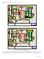
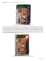
International Journal of Scientific and Research Publications, Volume 4, Issue 5, May 2014
ISSN 2250-3153
1
Implementation of Wind Turbine Controller Design for
Smart Campus
Aye Sandar Myint*, Hla Myo Tun*, Zaw Min Naing**
*
Department of Electronic Engineering, Mandalay Technological University
**
Technological University (Maubin)
Abstract- This paper presents the design and construction of charge controller for wind energy source. The charge controller is a small
prototype that is suitable to charge small battery. The maximum charging current of the charge controller is about 7 A. The charge
controller is designed using PIC 16F877A microcontroller, liquid-crystal display (LCD), silicon-controlled rectifier (SCR), rectifier
diodes and other electronic components. The SCR and rectifier diodes in conjunction with other components are used to charge the
battery. The battery charging is controlled by the microcontroller circuit. The LCD module displays the status of the battery while it is
charging. At the same time the voltage level of the battery is also displayed. The microcontroller controls the charging circuit and
diverted the charging current to the diverted load if the battery is fully charged. The microcontroller also produces signal to the audible
alarm circuit in the case of full charge battery. The simulation results are based on the ISIS software environments before
implementing the hardware description. The experimental results for charge controller are also mentioned.
Index Terms- wind turbine, controller, smart campus, renewable energy, PIC.
I. INTRODUCTION
A
S the importance of environmental protection and sustainable growth increases, wind energy, a clean and renewable energy,
attracts increasing attention. Wind energy is one of the most economical forms of alternative energy available today. It can save
the environment and make it cleaner for generations to come. This thesis is intended to emerge the charge controller for wind energy
source. A charge controller is an essential part for nearly all power systems that charge battery, whether the power source is solar,
wind, hydro, fuel, or utility grid. The charge controller can control the voltage and regulates the charging of the batteries. Its purpose
is to keep the batteries properly fed and safe for the long term. The basic functions of a controller are quite simple. Charge controllers
block the reverse current and prevent battery overcharge. Some charge controllers also prevent battery over discharge and protect from
electrical overload. The controllers also display the status of the battery. The main components of the wind energy system are the wind
turbine, the mechanical drive train, the generator, the power grid, and the controller. The wind turbine converts the kinetic energy of
the wind into mechanical energy. The generator converts the mechanical energy into electrical energy. The controller is the “brain” of
the system. It ensures that the whole system works as expected. The controller consists of two parts. The first part is the master
controller. The second part is the generator controller. During the power optimization stage, the master controller adjusts the system
rotation speed to keep the optimal tip speed ratio. The speed regulation works by controlling the power of the generator. During the
wind power limitation range, the master controller regulates the pitch angle to limit the wind power utilization. The generator
controller is in charge of accurately controlling the active power of the system. The generator controller adopts the stator flux oriented
vector control strategy. This thesis intends to propose and construct the charge controller portion of wind power system. The block
diagram of the wind power system is shown in Figure 1.1.
Wind
Drive
Train
Generator
Power
Grid
Controller
Figure 1. Block Diagram of Wind Power System
www.ijsrp.org
International Journal of Scientific and Research Publications, Volume 4, Issue 5, May 2014
ISSN 2250-3153
2
The charge controller for wind energy source is operated as: blocking reverse current, preventing overcharge, control set points vs.
temperature and control set points vs. battery type. In wind generator, the reverse current is controlled by using one kind of
semiconductor diode. The diode used for blocking reverse current is called a “blocking diode”. The overcharging of the battery can be
prevented by using pulse width modulation (PWM) controller. The ideal set points for charge controllers depend on the types of the
batteries. Some controllers have a means to select the type of battery.
II. PROPOSED CHARGE CONTROLLER
The charge controller intended to design and implement in this research work is a small power charge controller. Figure 2.6 shows the
block diagram of the charge controller. The charge controller is built around semiconductor switches (silicon controlled rectifier-SCR)
rather the electromechanical switches (relays). The microcontroller is used to control the overcharging of the battery, to display the
battery voltage continuously and to make audible alarm when the battery is fully charged. Firstly the battery is charged using high
current through the SCR. When the battery almost reaches its full terminal voltage (full charge) high current charging is cut off and
slow charging (trickle charging) is still done. At full charge condition the charging is totally cut out by the control of the
microcontroller. The current coming from the wind turbine through the converter circuit is diverting to another load (e.g. lamp). By
this means the overcharging of the battery is prevented. The constructed charge controller can charge the 12 V battery with up to 6 A
of current. The amount of charging current can be increased by changing some components in the charge controller without any
difficulty.
Power
Supply
From
Wind
Turbine
AC To DC
Converter
Load
(Lamp)
Battery
Charger
LCD Display
Voltage
Sense
Circuit
ADC Circuit
Alarm
PIC
Microcontroller
Figure 2. The Block Diagram of the Charge Controller
III. IMPLEMENTATION
The operation of the charge controller circuit is explained in this section. The charge controller circuit will charge the 12 V battery
until the battery gets its full terminal voltage. The charge controller changes from normal charging mode into the tickle charging mode
when the full terminal voltage (full charge) of the battery is reached. In the tickle charging mode the battery is slowly charged. The
charging of the battery is totally cut off by the control of microcontroller at the end. The battery full charge audible alarm is also
activated when the battery is fully charged. Therefore the damage of the battery from the overcharging can be avoided. The
components used in the circuit can withstand up to 6 A of charging current. This means that the power of the charge controller circuit
used in this research work is 6A x 12V = 72 W. By changing some components used in the circuit, the charge controller circuit can be
modified to charge the battery up to 300 A of charging current. Now it is the time to articulate the research work with ideas gathered
in above steps by adopting any of below suitable approaches.
At any time the voltage difference between the anode and the cathode of SCR1 is the instantaneous value of half sine wave and the
voltage of the battery. When the battery voltage is low the voltage difference between the anode and cathode of SCR1 is high. On the
other hand, the voltage difference between the anode and cathode of SCR1 will be low if the battery voltage is high. Therefore the
battery voltage becomes when the battery is charged. In this condition, the voltage difference between the anode and cathode of SCR1
tends to be low. This fact is the main idea of this charge controller circuit. The SCR controlled battery charger circuit is shown in
Figure 3.
www.ijsrp.org
International Journal of Scientific and Research Publications, Volume 4, Issue 5, May 2014
ISSN 2250-3153
3
D5
From
Rectifier
R1
470Ω
5W
PR1
220Ω
SCR1
C106D
D7
1N40
02
R3
47Ω
BATTERY
12V
PR2
1KΩ
R5 47Ω
2W
R6 47Ω
2W
SCR2
ZD1 C106D
11V/1W
C3
47uF
R4
1KΩ
Figure 3. The SCR Controlled Battery Charger Circuit
When the battery voltage is low the current flows into the gate terminal of SCR1 through resistor R5 and diode D7. Therefore the
SCR1 will conduct heavily for every half wave cycles and charges the battery with large currents. The voltage of the battery is sensed
(or detected) by the serially connected resistor R3 and the preset resistor PR2. The R3 and PR2 form voltage divider circuit. The PR2,
in this circuit, can be considered as two resistors: PR2 (u) and PR2 (l).
Therefore
PR2 = PR2 (u) + PR2 (l)
The total resistance RT above the center tap of PR2 is
RT = R3 + PR2 (u)
The voltage develops at the center tap of the preset PR2 (VPR2(l) ) can be calculated using the voltage divider equation:
VPR2(l) = ( PR2 (l) / RT + PR2 (l) ) VBattery
VPR2(l) = ( PR2 (l) / R3 + PR2 ) VBattery
The center tap of the preset resistor PR2 is connected to the cathode of the zener diode ZD1. The zener voltage of ZD1 is 11 V/1W.
The anode of the ZD1 is connected to the gate of SCR2. The SCR2 does not conduct if the voltage Vc develops at the center tap of the
PR2 is less than the zener voltage.
If the battery voltage becomes high due to the charging current the voltage V c will also high. If Vc becomes higher than the zener
voltage, the SCR2 will conduct for every half wave cycles. The conduction of SCR2 will start at 90 degree of the positive half cycle.
In the other word, it is the position for the largest charging current for the battery by the SCR1. Therefore large charging current is
shunt to the power resistors R5, R6 and SCR2.
In this condition SCR2 is conduct early than the SCR1. The voltage drop across the anode and cathode terminal of SCR2 will reduce
when the SCR2 is conducts heavily. Therefore the voltage between R5 and R6 becomes low and it makes the diode D7 reverse biased.
This causes the gate current of SCR1 stop. And therefore the conduction of SCR1 is stop. Therefore the charging of the battery
through SCR1 is stop.
The voltage between the anode and cathode of the SCR2 is approximately zero voltage when the SCR2 is heavily conducted. In this
condition the voltage at the junction of resistors R5 and R6 can be calculated by assuming the peak voltage of the rectifier output to be
about 16 V (VP = 16 V) as follows:
The voltage at the junction = ( R6 / R5 + R6) VP
= ( 47 / 47 + 47) 16 V
= 8V
The voltage is fed to the gate of the SCR1 via diode D7. The voltage is much lower than the cathode voltage of SCR1. Therefore
SCR1 is not conduct in this condition. The power ratings of the resistors R5 and R6 are 2 W respectively. They are chosen to
withstand the current passing through the heavily conducted SCR2.
Although there is no charging current to the battery through the SCR1 there is another charging current path to the battery. This is the
path formed by the diode D5, the resistor R1 and the preset resistor PR1. This is actually the slow charging current path (or trickle
charging). This prevents the battery from the overcharging.
The amount of slow charging current can be set by adjusting the preset resistor PR1. Similarly the full terminal voltage of the battery
can be set by adjusting the preset resistor PR2. The full terminal voltage for a 12 V battery is about 14.5 V
The port B pin (RB1) is configured as digital output pin. The RB1 normally produces logic ’0’ level while the battery is charging. The
RB1 will produce logic ’1’ when the full terminal voltage of the battery is get. The RB1 output pin is connected to the base of the
transistor TR1 through the current limiting resistor R. The emitter of the transistor is connected to the ground. The collector is
connected to the positive terminal of the battery through the relay coil. It is shown in Figure 4.4. The transistor is OFF when the RB1
www.ijsrp.org
International Journal of Scientific and Research Publications, Volume 4, Issue 5, May 2014
ISSN 2250-3153
4
pin is at logic ’0’ state. This is the charging state of the battery. In this state there is no current passing through the relay coil. So that
the relay switch is in the normally closed condition. As can be seen in circuit diagram, Figure 4, the normally closed switch of the
relay is connected between the diode rectifier output and charge control SCR circuit. In this condition the relay coil do not activate.
The relay will stay in this state until the full terminal voltage of the battery is arrived. At full terminal voltage the RB1 pin of the
microcontroller will produce logic ’1’ state. The voltage between the base-emitter junction of the transistor in forward bias condition
is about VBE = 0.7V.
To Charge Control
SCR Circuit
RELAY
From
Rectifier
Circuit
D6
1N4002
LOAD
TR1
C1013
12V
BATTERY
R2
RB1
10KΩ
Figure 4. The Relay Circuit for Charging and Load Diversion
The relay coil needs several mA of current to activate. And the current gain of the transistor is about 100. It is assumed that the relay
coil requires 40 mA to activate, the value of the base current limiting resistor can be calculated as follows:
Relay coil current = Collector current = IC = 40 mA
The base current IB of the transistor TR1 can be calculated using the equation:
IC = hFE IB
IB = IC / hFE
IB = 40 mA / 100 = 0.4 mA
The voltage drop across R2 can be calculated as follows:
V(R2) = 5 V - VBE
V(R2) = 5 V – 0.7 V = 4.3 V
The resistance of R2 can be calculated as follows:
R2 = V(R2) / IB = 4.3 V / 4 mA ≈ 10kΩ
The current IC is enough to drive the relay coil. Therefore the transistor is ON and the current is passing to the collector-emitter
junction of the transistor through the relay coil. Therefore the relay is activated and relay switch is connected to the normally open
connection. The load (lamp) is connected between the normally open terminal and ground. Therefore the current from the diode
rectifier will pass through the load to the ground. The current path from the rectifier to the SCR charge controller is cut out. The
battery will not be charged any more for this condition. This arrangement of the circuit prevents the battery from the over charging.
The audible alarm circuit is controlled by the port B pin (RB1). It is shown in Figure.5. The RB1 pin is connected with the base of
transistor TR2 through the current limiting resistor. While the battery is charging the RB1 pin output is logic ’0’ state and transistor
TR2 is OFF. Therefore the buzzer is not activated in this condition. The RB1 output is logic ’1’ state if the battery voltage reaches its
full terminal voltage (full charge). The transistor TR2 is turn ON. The buzzer produces audible alarm.
www.ijsrp.org
International Journal of Scientific and Research Publications, Volume 4, Issue 5, May 2014
ISSN 2250-3153
5
5V
D8
1N4002
BUZZER
TR2
C1013
R9
RB1
10KΩ
Figure.5. The Audible Alarm Circuit
The buzzer requires about 40 mA of current to activate. The current gain of the transistor is about 100. The value of the base current
limiting resistor can be calculated as follows:
Collector current = IC = 40 mA
The base current IB of the transistor TR2 can be calculated using the equation:
IC = hFE IB
IB = IC / hFE
IB = 40 mA / 100 = 0.4 mA
The voltage drop across R9 can be calculated as follows:
V(R9) = 5 V - VBE
V(R9) = 5 V – 0.7 V = 4.3 V
The resistance of R9 can be calculated as follows:
R9 = V(R9) / IB = 4.3 V / 4 mA ≈ 10kΩ
The current IC is enough to drive the buzzer. Therefore the current is passing from the + 5 V supply to the ground through the buzzer
and collector and emitter junction of the transistor TR2. Thus the audible alarm is activated when the battery is fully charged.
The flow chart of the charge controller is shown in Fig. 4.9. At the start of the program, the I/O port directions of the microcontroller
are set. The full charge voltage of the battery is assigned and stored in the memory of the microcontroller as V bf.
Start
Set Port Direction
Set ADC Input
Full Charge Volt Vbf
Display
“Battery Voltage”
At Upper Line of LCD
Is Vbc >= Vbf ?
No
Yes
Battery Charging
Charging Cut Off
Alarm ON, Relay ON
Display
“Full Charge”
At Lower Line of LCD
Display
“---V”
At Lower Line of LCD
Stop
Figure 6. The Flow Chart Diagram of the Charge Controller
www.ijsrp.org
International Journal of Scientific and Research Publications, Volume 4, Issue 5, May 2014
ISSN 2250-3153
6
The ADC section of the microcontroller is enabled and RA0 pin is assigned as the ADC input pin. The resolution of the ADC is set at
10 bits and the reference voltage for the ADC is assigned as +5V. Then the PIC microcontroller pins, used to send control and data
signals to the LCD module, are defined according to the PIC BASIC PRO compiler specifications.
In this paper, 4-bit mode is used to display data and message on the LCD module. The upper line of the 16×2 lines LCD module
displays the message "Battery Voltage". The charging battery voltage, V bc at RA0 is checked by the program. The battery voltage is
displayed on the lower line as "- - - V". And then the battery voltage is compared with the battery full charge voltage. If the battery
voltage is less than the full charge voltage the battery charging is going on. On the other hand, if the battery voltage is equal to or
greater than the full charge voltage, the charging of the battery is completely stopped. Then the lower line of the LCD will display
“Full Charge”. The program waits about 1s and then loop back to the start of the voltage comparison statement.
The program source code for the PIC microcontroller is developed in Micro Code Studio (IDE). The software is configured to work
together with PIC BASIC PRO complier software and EPICWIN programmer software. Therefore all steps of software routines,
editing the source code, compiling the source code into Hex file and programming the Hex file into microcontroller's flash memory
can be done in Micro Code Studio software. The programmer hardware used for this paper is EPIC Plus programmer board from
micro Engineering Labs Inc. EPIC Plus is a low-cost programmer with an 18-pin socket on the device. The programmer is connected
to the parallel part (the printer port) of a PC using a 25-way DB 25 type cable
IV. SIMULATION RESULTS
At first, the charge controller circuit is simulated using Proteus software.
The schematic diagram of the main components of
the charge controller circuit including the microcontroller circuit is drawn in the ISIS software and then run the simulator program. A
screenshot of the ISIS schematic capture and interactive simulation environment is shown in Figure 7.
Figure 7. The ISIS Screenshot of the Charge Controller Circuit
The simulated result of the program for the charging and full charge conditions are shown in Figure 8 and Figure 8, respectively.
www.ijsrp.org
International Journal of Scientific and Research Publications, Volume 4, Issue 5, May 2014
ISSN 2250-3153
7
U1
LCD1
7805
D5
1
47
D7
1
2
3
1N4002
220
D0
D1
D2
D3
D4
D5
D6
D7
RS
RW
E
C106D
7
8
9
10
11
12
13
14
VSS
VDD
VEE
PR1
4
5
6
SCR1
470
3
2
R1
GDM1602A
VO
GND
R5
VI
U2
R3
+12.0
47
Volts
R6
R7
47
47k
13
14
1
BAT1
ZD1
PR2
2
3
4
5
6
7
SCR2
C106D
1N4741A
C3
R4
47u
1K
8
9
10
PR3
VSINE
OSC1/CLKIN
OSC2/CLKOUT
MCLR/Vpp/THV
RB0/INT
RB1
RB2
RB3/PGM
RB4
RB5
RB6/PGC
RB7/PGD
RA0/AN0
RA1/AN1
RA2/AN2/VREFRA3/AN3/VREF+
RA4/T0CKI
RA5/AN4/SS
RC0/T1OSO/T1CKI
RC1/T1OSI/CCP2
RE0/AN5/RD
RC2/CCP1
RE1/AN6/WR
RC3/SCK/SCL
RE2/AN7/CS
RC4/SDI/SDA
RC5/SDO
RC6/TX/CK
RC7/RX/DT
V1
RD0/PSP0
RD1/PSP1
RD2/PSP2
RD3/PSP3
RD4/PSP4
RD5/PSP5
RD6/PSP6
RD7/PSP7
+3.58
Volts
RL1
LOAD LAMP
+14.1
12V
AC Volts
33
34
35
36
37
38
39
40
15
16
17
18
23
24
25
26
D8
BUZ1
BUZZER
1N4002
19
20
21
22
27
28
29
30
PIC16F877A
G2R-14-DC5
BR1
TR1
D1-D4
R2
R9
47k
10K
TR2
2SC1013
C1
47u
2SC1013
DESIGN AND CONSTRUCTION OF CHARGE CONTROLLER FOR WIND ENERGY SOURCE
TECHNOLOGY UNIVERSITY
BY
MANDALAY
MA WAI HLAING MAR
M.E (THESIS)
2010
Figure 8 Screenshot of Charging Condition
U1
LCD1
7805
D5
1
47
D7
1
2
3
1N4002
D0
D1
D2
D3
D4
D5
D6
D7
7
8
9
10
11
12
13
14
C106D
220
RS
RW
E
VSS
VDD
VEE
PR1
3
4
5
6
SCR1
470
VO
2
R1
GDM1602A
VI
GND
R5
U2
R3
+15.0
47
Volts
R6
R7
47
47k
13
14
1
BAT1
ZD1
PR2
2
3
4
5
6
7
SCR2
C106D
1N4741A
C3
R4
47u
1K
8
9
10
PR3
VSINE
OSC1/CLKIN
OSC2/CLKOUT
MCLR/Vpp/THV
RA0/AN0
RA1/AN1
RA2/AN2/VREFRA3/AN3/VREF+
RA4/T0CKI
RA5/AN4/SS
RC0/T1OSO/T1CKI
RC1/T1OSI/CCP2
RE0/AN5/RD
RC2/CCP1
RE1/AN6/WR
RC3/SCK/SCL
RE2/AN7/CS
RC4/SDI/SDA
RC5/SDO
RC6/TX/CK
RC7/RX/DT
V1
RD0/PSP0
RD1/PSP1
RD2/PSP2
RD3/PSP3
RD4/PSP4
RD5/PSP5
RD6/PSP6
RD7/PSP7
+4.47
Volts
RL1
LOAD LAMP
+14.1
12V
AC Volts
RB0/INT
RB1
RB2
RB3/PGM
RB4
RB5
RB6/PGC
RB7/PGD
33
34
35
36
37
38
39
40
15
16
17
18
23
24
25
26
D8
BUZ1
BUZZER
1N4002
19
20
21
22
27
28
29
30
PIC16F877A
G2R-14-DC5
BR1
TR1
D1-D4
R2
R9
47k
10K
TR2
2SC1013
C1
47u
2SC1013
TECHNOLOGY UNIVERSITY
MANDALAY
DESIGN AND CONSTRUCTION OF CHARGE CONTROLLER FOR WIND ENERGY SOURCE
BY
MA WAI HLAING MAR
M.E (THESIS)
2010
Figure 9 Screenshot of Full Charge Condition
V. EXPERIMENTAL RESULTS OF THE CHARGE CONTROLLER
At first the charge controller is firstly tested with the wind power generator. The wind power generator with blade diameter of 2m can
produce an electrical average power output of about 50 W in the wind speed of about 10 miles per hour. But the wind speed is hanging
www.ijsrp.org
International Journal of Scientific and Research Publications, Volume 4, Issue 5, May 2014
ISSN 2250-3153
8
with time and whether conditions. Sometimes it is calm and there is no power output from the wind power generator. Therefore it is
not convenient to test the charge controller with the electrical power produced by the wind power generator for every time.
The charge controller is tested with the step-down AC transformer with the same power rating as the wind power generator in the
place of the AC generator of the wind electric power generator. The battery can be charged according to the charge controller. The
charging current of the battery is limited to the maximum of 6A. The presets used in the circuit are adjusted to fulfill the requirements
stated in the previous chapters. The LCD module displays the messages about the voltage of the battery for every second while it is
charging. Figures 10, 11 and 12 show the photos of the complete circuit of the charge controller for charging stage. The first line of
the LCD module displays the message “BATTERY VOLTAGE” and the second line displays the battery voltage.
Figure 10. Photo of the Charge Controller in the Charging Stage (9V)
Figure 11. Photo of the Charge Controller in the Charging Stage (10V)
www.ijsrp.org
International Journal of Scientific and Research Publications, Volume 4, Issue 5, May 2014
ISSN 2250-3153
9
Figure 12. Photo of the Charge Controller in the Charging Stage (12V)
There are two paths for the battery charging stage. The first one is through the SCR1. It is the main charging path for the battery. The
large current of about 6A is allowed for fast charging. The second one is through the diode D5, resistor R1 and preset resistor PR1.
This is the slow charging path and the charging current depends on the values of resistor and preset resistor. When the battery is
almost fully charged the SCR1 is cut off and there is no charging from this path. But there is still slow charging from the second path.
The charging current is totally cut off when the battery is fully charged. The electrical power delivers from the transformer is diverted
to the load (light bulb in this research). The photo of the LCD screen for the fully charged condition is shown in Figure 12. The first
line of LCD module displays “BATTERY VOLTAGE”. The second line displays the message “FULL CHARGE”. Photo of the
complete circuit board for the fully charged stage is shown in Figure 13.
Figure 13. Photo of the Complete Circuit Board for the Fully Charged Stage
www.ijsrp.org
International Journal of Scientific and Research Publications, Volume 4, Issue 5, May 2014
ISSN 2250-3153
10
The charging time for the 100AH battery using this charge controller will be about 20 hours for fully charged if enough electrical
power is obtained from the source (wind energy). The advantage of using the charge controller is to protect the battery from over
charging. The constructed charge controller can perform the battery charging and protection from the over charging. The charge
controller will also make audible alarm if the battery is fully charged. As a future research, the charge controller can be designed to
withstand higher charging current by using appropriate electronic components.
VI. CONCLUSION
The charge controller in the present circuit can control maximum charging current of about 7 A. It is not large enough to charge
battery with large ampere hour rating (e.g. 120 AH, 150 AH). The charging time for large battery will take more than ten hours. It
takes a long time to charge the battery. So it is not practical to use this type of charge controller for large battery. Therefore, the
current rating of the charge controller must be increased to be suitable for real world applications. The charge controller operation is
based on the semiconductor device (SCR). The current rating of the SCR used in the circuit is about 8 A. Therefore, the charging
current cannot exceed the limiting current value of the SCR. The electronic components used in the charge controller are chosen to
reduce costs and to experiment easily. The constructed charge controller is intended to demonstrate the charging and over charge
control circuits with the help of microcontroller. Therefore, some modifications must be made to be useful practically.
ACKNOWLEDGMENT
I would wish to acknowledge the many colleagues at Mandalay Technological University who have contributed to the development
of this paper.
REFERENCES
[1]
Ferreira P., et al.: Interfaces for Renewable Energy Sources with Electric Power Systems, Environment 2010: Situation and Perspectives for the European Union
6-10 May 2003. Porto, Portugal
[2] Anonymous: Wind Turbines for Home Power, June 2010, http://www.absak.com/library/wind-turbine-home-power
[3] Anonymous: Xantrex Charge Controllers, June 2010, http://www.enviroharvest.co.za
[4] Anonymous: WTCC Specification – Wind Turbine Charge Controller (WTCC), May 2010, http://www.environmentsaveenergy.co.za/WTCC%20specifications
[5] Anonymous: Kestrel Charge Controller Type 0801 User Manual, May 2010, http://www.kestrelwind.co.za
[6] Anonymous: GDM 1602A Liquid Crystal Display (LCD) Data Sheet, XIAMEN OCULAR, http://www.xmocular.com/MODULE/GDC1602A.htm
[7] Nelson V.: WIND ENERGY: Renewable Energy and the Environment, CRC Press, (2009).
[8] Hugh P.: Home-Build Windpower, January 2007, http://www.scoraigwind.com/books/
[9] Ibrahim D.: PIC BASIC Projects, Elsevier, (2006).
[10] Bates M.: INTERFACING PIC MICROCONTROLLERS: Embedded Design by Interactive Simulation, Elsevier, (2006).
http://www.labcenter.co.uk
[11] Anonymous: PIC 16F87XA Data Sheet, Microchip Technology Inc., 2001, https://www.microchip.com
www.ijsrp.org