1
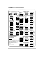
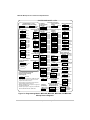
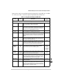
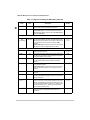
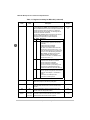
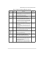
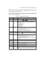
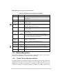
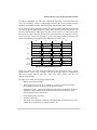
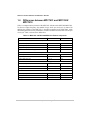
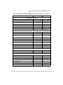
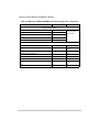
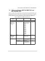
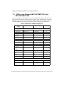
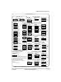
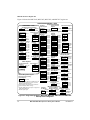
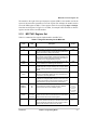
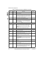
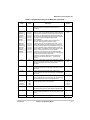
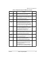
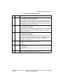
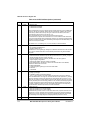
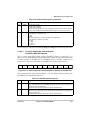
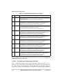
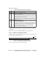
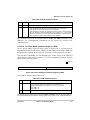
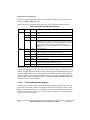
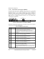
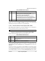
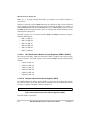
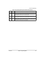
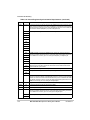
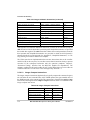
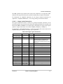
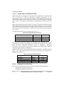
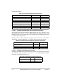
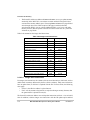
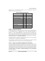
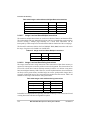
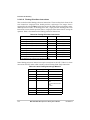
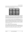
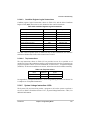
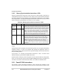
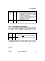
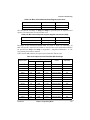
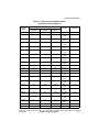
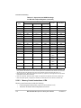
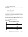
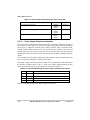
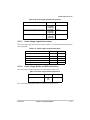
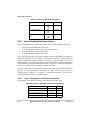
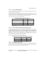
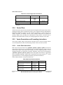
AltiVec UISA Instructions
Table 2-74. Vector Integer Arithmetic Instructions (continued)
Name
Mnemonic
Syntax
Vector Maximum Signed Integer
vmaxsb
vmaxsh
vmaxsw
vD,vA,vB
Vector Minimum Unsigned Integer
vminub
vminuh
vminuw
vD,vA,vB
Vector Minimum Signed Integer
vminsb
vminsh
vminsw
vD,vA,vB
2.5.1.2
Vector Integer Compare Instructions
The vector integer compare instructions algebraically or logically compare the contents of
the elements in vector register vA with the contents of the elements in vB. Each compare
result vector is comprised of TRUE (0xFF, 0xFFFF, 0xFFFF_FFFF) or FALSE (0x00,
0x0000, 0x0000_0000) elements of the size specified by the compare source operand
element (byte, half word, or word). The result vector can be directed to any VR and can be
manipulated with any of the instructions as normal data (for example, combining condition
results).
Vector compares provide equal-to and greater-than predicates. Others are synthesized from
these by logically combining or inverting result vectors.
The integer compare instructions (shown in Table 2-76) can optionally set the CR6 field of
the PowerPC condition register. If Rc = 1 in the vector integer compare instruction, then
CR6 is set to reflect the result of the comparison, as follows in Table 2-75.
Table 2-75. CR6 Field Bit Settings for Vector Integer Compare Instructions
CR Bit
CR6 Bit
Vector Compare
24
0
1 Relation is true for all element pairs (that is, vD is set to all ones)
25
1
0
26
2
1 Relation is false for all element pairs (that is, register vD is cleared)
27
3
0
Table 2-76 summarizes the vector integer compare instructions.
2-106
MPC7450 RISC Microprocessor Family User’s Manual
MOTOROLA