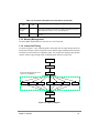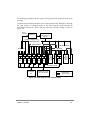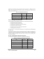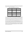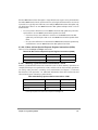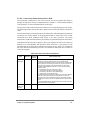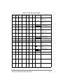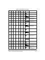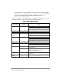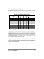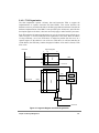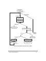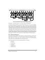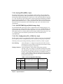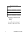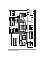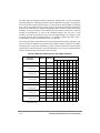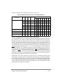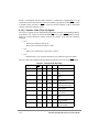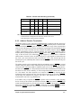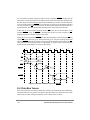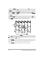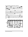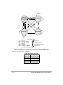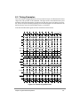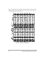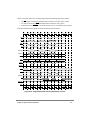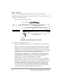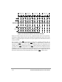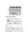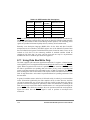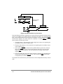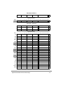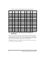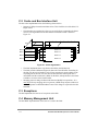
1
Overview
1
Programming Model
2
Cache and Bus Interface Unit Operation
3
Exceptions
4
Memory Management
5
Instruction Timing
6
Signal Descriptions
7
System Interface Operation
8
Performance Monitor
9
PowerPC Instruction Set Listings
A
Invalid Instruction Forms
B
PowerPC 604 Processor System Design
and Programming Considerations
C
Glossary GLO
Index
IND
1
Overview
2
Programming Model
3
Cache and Bus Interface Unit Operation
4
Exceptions
5
Memory Management
6
Instruction Timing
7
Signal Descriptions
8
System Interface Operation
9
Performance Monitor
A
PowerPC Instruction Set Listings
B
Invalid Instruction Forms
C
PowerPC 604 Processor System Design
and Programming Considerations
GLO
Glossary
IND
Index
G522-0330-00
MPC604EUM/AD
3/98
PowerPC 604e
™
RISC Microprocessor User's Manual
with Supplement for PowerPC 604™ Microprocessor
.
This document contains information on a new product under development. Motorola reserves the right to change or discontinue this product without notice.
Information in this document is provided solely to enable system and software implementers to use PowerPC microprocessors. There are no express or
implied copyright licenses granted hereunder to design or fabricate PowerPC integrated circuits or integrated circuits based on the information in this
document.
The PowerPC 604e microprocessor embodies the intellectual property of IBM and of Motorola. However, neither party assumes any responsibility or
liability as to any aspects of the performance, operation, or other attributes of the microprocessor as marketed by the other party. Neither party is to be
considered an agent or representative of the other party, and neither has granted any right or authority to the other to assume or create any express or
implied obligations on its behalf. Information such as data sheets, as well as sales terms and conditions such as prices, schedules, and support, for the
microprocessor may vary as between IBM and Motorola. Accordingly, customers wishing to learn more information about the products as marketed by a
given party should contact that party.
Both IBM and Motorola reserve the right to modify this manual and/or any of the products as described herein without further notice. Nothing in this
manual, nor in any of the errata sheets, data sheets, and other supporting documentation, shall be interpreted as conveying an express or implied
warranty, representation, or guarantee regarding the suitability of the products for any particular purpose. The parties do not assume any liability or
obligation for damages of any kind arising out of the application or use of these materials. Any warranty or other obligations as to the products described
herein shall be undertaken solely by the marketing party to the customer, under a separate sale agreement between the marketing party and the customer.
In the absence of such an agreement, no liability is assumed by the marketing party for any damages, actual or otherwise.
“Typical” parameters can and do vary in different applications. All operating parameters, including “Typicals,” must be validated for each customer
application by customer’s technical experts. Neither IBM nor Motorola convey any license under their respective intellectual property rights nor the rights
of others. The products described in this manual are not designed, intended, or authorized for use as components in systems intended for surgical implant
into the body, or other applications intended to support or sustain life, or for any other application in which the failure of the product could create a situation
where personal injury or death may occur. Should customer purchase or use the products for any such unintended or unauthorized application, customer
shall indemnify and hold IBM and Motorola and their respective officers, employees, subsidiaries, affiliates, and distributors harmless against all claims,
costs, damages, and expenses, and reasonable attorney fees arising out of, directly or indirectly, any claim of personal injury or death associated with
such unintended or unauthorized use, even if such claim alleges that Motorola or IBM was negligent regarding the design or manufacture of the part.
Motorola and
are registered trademarks of Motorola, Inc. Motorola, Inc. is an Equal Opportunity/Affirmative Action Employer.
The PowerPC name, the PowerPC logotype, PowerPC 601, PowerPC 603, PowerPC 603e, PowerPC 604, and PowerPC 604e are trademarks of
International Business Machines Corporation used by Motorola under license from International Business Machines Corporation.
© Motorola Inc. 1998. All rights reserved.
Portions hereof © International Business Machines Corp. 1991–1998. All rights reserved.
CONTENTS
Paragraph
Number
Title
Page
Number
About This Book
Audience ............................................................................................................ xxiv
Organization.........................................................................................................xxv
Suggested Reading............................................................................................. xxvi
General Information.......................................................................................... xxvi
PowerPC Documentation.................................................................................. xxvi
Conventions ..................................................................................................... xxviii
Acronyms and Abbreviations ............................................................................ xxix
Terminology Conventions ................................................................................ xxxii
Chapter 1
Overview
1.1
1.2
1.3
1.3.1
1.3.2
1.3.2.1
1.3.2.2
1.3.2.3
1.3.3
1.3.3.1
1.3.3.2
1.3.3.3
1.3.4
1.3.5
1.3.6
1.3.7
1.3.8
1.3.9
Overview.............................................................................................................. 1-1
PowerPC 604e Microprocessor Features ............................................................. 1-2
PowerPC Architecture Implementation ............................................................... 1-8
Features............................................................................................................ 1-9
PowerPC 604e Processor Programming Model............................................. 1-10
Implementation-Specific Registers............................................................ 1-10
Support for Misaligned Little-Endian Accesses ........................................ 1-12
Instruction Set ............................................................................................ 1-13
Cache and Bus Interface Unit Operation ....................................................... 1-14
Instruction Cache ....................................................................................... 1-14
Data Cache................................................................................................. 1-15
Additional Changes to the Cache .............................................................. 1-15
Exceptions...................................................................................................... 1-16
Memory Management.................................................................................... 1-21
Instruction Timing ......................................................................................... 1-21
Signal Descriptions ........................................................................................ 1-24
System Interface Operation .......................................................................... 1-27
Performance Monitor..................................................................................... 1-28
Chapter 2
Programming Model
2.1
2.1.1
2.1.2
2.1.2.1
2.1.2.2
2.1.2.3
Contents
Register Set .......................................................................................................... 2-1
Register Set ...................................................................................................... 2-2
PowerPC 604e-Specific Registers ................................................................... 2-8
Instruction Address Breakpoint Register (IABR)........................................ 2-9
Processor Identification Register (PIR) ....................................................... 2-9
Hardware Implementation-Dependent Register 0 ..................................... 2-10
v
CONTENTS
Paragraph
Number
2.1.2.4
2.1.2.5
2.1.2.5.1
2.1.2.5.2
2.1.2.5.3
2.1.2.5.4
2.1.2.5.5
2.1.3
2.2
2.2.1
2.2.2
2.2.3
2.2.4
2.2.5
2.2.6
2.3
2.3.1
2.3.1.1
2.3.1.2
2.3.1.3
2.3.1.4
2.3.2
2.3.2.1
2.3.2.2
2.3.2.3
2.3.2.4
2.3.2.4.1
2.3.2.4.2
2.3.2.4.3
2.3.3
2.3.4
2.3.4.1
2.3.4.1.1
2.3.4.1.2
2.3.4.1.3
2.3.4.1.4
2.3.4.2
2.3.4.2.1
2.3.4.2.2
2.3.4.2.3
2.3.4.2.4
2.3.4.2.5
2.3.4.2.6
vi
Title
Page
Number
Hardware Implementation-Dependent Register 1 (HID1) ........................ 2-12
Performance Monitor Registers ................................................................. 2-12
Monitor Mode Control Register 0 (MMCR0) ....................................... 2-13
Monitor Mode Control Register 1—MMCR1....................................... 2-14
Performance Monitor Counter Registers (PMC1–PMC4) .................... 2-15
Sampled Instruction Address Register (SIA) ........................................ 2-20
Sampled Data Address Register (SDA)................................................. 2-21
Reset Settings................................................................................................. 2-21
Operand Conventions......................................................................................... 2-22
Floating-Point Execution Models—UISA..................................................... 2-22
Data Organization in Memory and Data Transfers........................................ 2-23
Alignment and Misaligned Accesses............................................................. 2-23
Support for Misaligned Little-Endian Accesses ............................................ 2-23
Floating-Point Operand.................................................................................. 2-24
Effect of Operand Placement on Performance .............................................. 2-26
Instruction Set Summary.................................................................................... 2-26
Classes of Instructions ................................................................................... 2-28
Definition of Boundedly Undefined .......................................................... 2-28
Defined Instruction Class .......................................................................... 2-28
Illegal Instruction Class ............................................................................. 2-29
Reserved Instruction Class ........................................................................ 2-30
Addressing Modes ......................................................................................... 2-30
Memory Addressing .................................................................................. 2-30
Memory Operands ..................................................................................... 2-30
Effective Address Calculation ................................................................... 2-31
Synchronization ......................................................................................... 2-31
Context Synchronization ....................................................................... 2-31
Execution Synchronization.................................................................... 2-32
Instruction-Related Exceptions.............................................................. 2-32
Instruction Set Overview ............................................................................... 2-33
PowerPC UISA Instructions .......................................................................... 2-33
Integer Instructions .................................................................................... 2-33
Integer Arithmetic Instructions.............................................................. 2-33
Integer Compare Instructions ................................................................ 2-35
Integer Logical Instructions................................................................... 2-35
Integer Rotate and Shift Instructions ..................................................... 2-36
Floating-Point Instructions ........................................................................ 2-37
Floating-Point Arithmetic Instructions .................................................. 2-37
Floating-Point Multiply-Add Instructions ............................................. 2-38
Floating-Point Rounding and Conversion Instructions ......................... 2-38
Floating-Point Compare Instructions..................................................... 2-39
Floating-Point Status and Control Register Instructions ....................... 2-39
Floating-Point Move Instructions .......................................................... 2-40
PowerPC 604e RISC Microprocessor User’s Manual
CONTENTS
Paragraph
Number
2.3.4.3
2.3.4.3.1
2.3.4.3.2
2.3.4.3.3
2.3.4.3.4
2.3.4.3.5
2.3.4.3.6
2.3.4.3.7
2.3.4.3.8
2.3.4.3.9
2.3.4.4
2.3.4.4.1
2.3.4.4.2
2.3.4.4.3
2.3.4.4.4
2.3.4.5
2.3.4.6
2.3.4.6.1
2.3.4.6.2
2.3.4.7
2.3.5
2.3.5.1
2.3.5.2
2.3.5.3
2.3.5.3.1
2.3.5.4
2.3.6
2.3.6.1
2.3.6.2
2.3.6.3
2.3.6.3.1
2.3.6.3.2
2.3.6.3.3
2.3.7
Title
Page
Number
Load and Store Instructions ....................................................................... 2-40
Self-Modifying Code ............................................................................. 2-41
Integer Load and Store Address Generation.......................................... 2-41
Register Indirect Integer Load Instructions ........................................... 2-42
Integer Store Instructions....................................................................... 2-43
Integer Load and Store with Byte Reverse Instructions ........................ 2-44
Integer Load and Store Multiple Instructions........................................ 2-44
Integer Load and Store String Instructions............................................ 2-45
Floating-Point Load and Store Address Generation.............................. 2-47
Floating-Point Store Instructions........................................................... 2-48
Branch and Flow Control Instructions....................................................... 2-50
Branch Instruction Address Calculation................................................ 2-50
Branch Instructions................................................................................ 2-50
Condition Register Logical Instructions................................................ 2-51
Trap Instructions.................................................................................... 2-51
System Linkage Instruction—UISA.......................................................... 2-52
Processor Control Instructions—UISA ..................................................... 2-52
Move to/from Condition Register Instructions...................................... 2-52
Move to/from Special-Purpose Register Instructions (UISA)............... 2-53
Memory Synchronization Instructions—UISA ......................................... 2-53
PowerPC VEA Instructions ........................................................................... 2-54
Processor Control Instructions—VEA ...................................................... 2-55
Memory Synchronization Instructions—VEA .......................................... 2-55
Memory Control Instructions—VEA ........................................................ 2-56
User-Level Cache Instructions—VEA .................................................. 2-57
Optional External Control Instructions...................................................... 2-59
PowerPC OEA Instructions ........................................................................... 2-59
System Linkage Instructions—OEA ......................................................... 2-59
Processor Control Instructions—OEA ...................................................... 2-59
Memory Control Instructions—OEA ........................................................ 2-61
Supervisor-Level Cache Management Instruction—(OEA) ................. 2-61
Segment Register Manipulation Instructions (OEA)............................. 2-61
Translation Lookaside Buffer Management Instructions—(OEA) ....... 2-62
Recommended Simplified Mnemonics.......................................................... 2-63
Chapter 3
Cache and Bus Interface Unit Operation
3.1
3.2
3.3
3.4
Contents
Data Cache Organization ..................................................................................... 3-4
Instruction Cache Organization ........................................................................... 3-5
MMUs/Bus Interface Unit ................................................................................... 3-6
Memory Coherency Actions ................................................................................ 3-9
vii
CONTENTS
Paragraph
Number
3.4.1
3.4.2
3.5
3.5.1
3.5.2
3.5.3
3.6
3.6.1
3.6.2
3.6.3
3.6.4
3.6.5
3.6.6
3.7
3.8
3.8.1
3.8.2
3.8.3
3.8.4
3.8.5
3.8.6
3.8.7
3.9
3.9.1
3.9.2
3.9.3
3.9.4
3.9.5
3.9.6
3.9.7
3.9.8
3.9.9
3.10
3.11
Title
Page
Number
PowerPC 604e-Initiated Load and Store Operations....................................... 3-9
General Comments on Snooping ................................................................... 3-10
Sequential Consistency ...................................................................................... 3-11
Sequential Consistency Within a Single Processor ....................................... 3-11
Weak Consistency between Multiple Processors .......................................... 3-11
Sequential Consistency Within Multiprocessor Systems .............................. 3-12
Memory and Cache Coherency.......................................................................... 3-12
Data Cache Coherency Protocol .................................................................... 3-13
Coherency and Secondary Caches................................................................. 3-15
Page Table Control Bits................................................................................. 3-15
MESI State Diagram...................................................................................... 3-15
Coherency Paradoxes in Single-Processor Systems ...................................... 3-16
Coherency Paradoxes in Multiple-Processor Systems................................... 3-17
Cache Configuration .......................................................................................... 3-17
Cache Control Instructions ................................................................................ 3-18
Instruction Cache Block Invalidate (icbi)...................................................... 3-18
Instruction Synchronize (isync)..................................................................... 3-19
Data Cache Block Touch (dcbt) and Data Cache Block Touch
for Store (dcbtst) ....................................................................................... 3-19
Data Cache Block Set to Zero (dcbz)............................................................ 3-19
Data Cache Block Store (dcbst) .................................................................... 3-20
Data Cache Block Flush (dcbf) ..................................................................... 3-20
Data Cache Block Invalidate (dcbi) .............................................................. 3-20
Basic Cache Operations ..................................................................................... 3-20
Cache Reloads................................................................................................ 3-20
Cache Cast-Out Operation ............................................................................. 3-21
Cache Block Push Operation ......................................................................... 3-21
Atomic Memory References.......................................................................... 3-21
Snoop Response to Bus Operations ............................................................... 3-22
Cache Reaction to Specific Bus Operations .................................................. 3-22
Enveloped High-Priority Cache Block Push Operation ................................ 3-25
Bus Operations Caused by Cache Control Instructions................................. 3-26
Cache Control Instructions ............................................................................ 3-26
Cache Actions .................................................................................................... 3-27
Access to Direct-Store Segments....................................................................... 3-48
Chapter 4
Exceptions
4.1
4.2
4.3
4.3.1
viii
PowerPC 604e Microprocessor Exceptions......................................................... 4-2
Exception Recognition and Priorities .................................................................. 4-5
Exception Processing ........................................................................................... 4-6
Enabling and Disabling Exceptions................................................................. 4-9
PowerPC 604e RISC Microprocessor User’s Manual
CONTENTS
Paragraph
Number
4.3.2
4.3.3
4.3.4
4.4
4.5
4.5.1
4.5.2
4.5.2.1
4.5.2.2
4.5.3
4.5.4
4.5.5
4.5.6
4.5.7
4.5.8
4.5.9
4.5.10
4.5.11
4.5.12
4.5.13
4.5.14
4.5.15
4.5.16
Title
Page
Number
Steps for Exception Processing...................................................................... 4-10
Setting MSR[RI] ............................................................................................ 4-11
Returning from an Exception Handler........................................................... 4-11
Process Switching .............................................................................................. 4-11
Exception Definitions ........................................................................................ 4-12
System Reset Exception (0x00100)............................................................... 4-13
Machine Check Exception (0x00200) ........................................................... 4-14
Machine Check Exception Enabled (MSR[ME] = 1)................................ 4-15
Checkstop State (MSR[ME] = 0) .............................................................. 4-16
DSI Exception (0x00300) .............................................................................. 4-16
ISI Exception (0x00400)................................................................................ 4-16
External Interrupt Exception (0x00500) ........................................................ 4-16
Alignment Exception (0x00600) ................................................................... 4-17
Program Exception (0x00700)....................................................................... 4-18
Floating-Point Unavailable Exception (0x00800) ......................................... 4-19
Decrementer Exception (0x00900)................................................................ 4-19
System Call Exception (0x00C00) ................................................................ 4-19
Trace Exception (0x00D00)........................................................................... 4-19
Floating-Point Assist Exception (0x00E00) .................................................. 4-20
Performance Monitoring Interrupt (0x00F00)............................................... 4-20
Instruction Address Breakpoint Exception (0x01300) .................................. 4-21
System Management Interrupt (0x01400) ..................................................... 4-21
Power Management ....................................................................................... 4-21
Chapter 5
Memory Management
5.1
5.1.1
5.1.2
5.1.3
5.1.4
5.1.5
5.1.6
5.1.6.1
5.1.6.2
5.1.6.2.1
5.1.6.2.2
5.1.7
5.1.8
5.1.9
5.2
MMU Overview................................................................................................... 5-2
Memory Addressing ........................................................................................ 5-4
MMU Organization.......................................................................................... 5-4
Address Translation Mechanisms.................................................................... 5-9
Memory Protection Facilities......................................................................... 5-11
Page History Information............................................................................... 5-12
General Flow of MMU Address Translation................................................. 5-12
Real Addressing Mode and Block Address Translation Selection ............ 5-12
Page and Direct-Store Interface Address Translation Selection............... 5-14
Selection of Page Address Translation .................................................. 5-16
Selection of Direct-Store Interface Address Translation....................... 5-16
MMU Exceptions Summary .......................................................................... 5-16
MMU Instructions and Register Summary.................................................... 5-18
TLB Entry Invalidation.................................................................................. 5-20
Real Addressing Mode....................................................................................... 5-20
Contents
ix
CONTENTS
Paragraph
Number
5.3
5.4
5.4.1
5.4.1.1
5.4.1.2
5.4.1.3
5.4.2
5.4.3
5.4.3.1
5.4.3.2
5.4.4
5.4.5
5.4.6
5.4.7
5.5
5.5.1
5.5.2
5.5.3
5.5.4
5.5.5
Title
Page
Number
Block Address Translation................................................................................. 5-20
Memory Segment Model ................................................................................... 5-20
Page History Recording ................................................................................. 5-21
Referenced Bit ........................................................................................... 5-22
Changed Bit ............................................................................................... 5-22
Scenarios for Referenced and Changed Bit Recording ............................. 5-23
Page Memory Protection ............................................................................... 5-24
TLB Description ............................................................................................ 5-24
TLB Organization ...................................................................................... 5-25
TLB Invalidation ....................................................................................... 5-26
Page Address Translation Summary.............................................................. 5-28
Page Table Search Operation......................................................................... 5-30
Page Table Updates ....................................................................................... 5-34
Segment Register Updates ............................................................................. 5-35
Direct-Store Interface Address Translation ....................................................... 5-35
Direct-Store Interface Accesses..................................................................... 5-35
Direct-Store Segment Protection ................................................................... 5-36
Instructions Not Supported in Direct-Store Segments................................... 5-36
Instructions with No Effect in Direct-Store Segments .................................. 5-36
Direct-Store Segment Translation Summary Flow........................................ 5-37
Chapter 6
Instruction Timing
6.1
6.2
6.2.1
6.2.1.1
6.2.1.1.1
6.2.1.1.2
6.2.1.1.3
6.2.1.1.4
6.2.1.1.5
6.2.1.1.6
6.3
6.3.1
6.3.2
6.3.3
6.3.4
6.3.4.1
6.3.4.2
6.3.4.3
6.4
x
Terminology and Conventions............................................................................. 6-1
Instruction Timing Overview............................................................................... 6-3
Pipeline Structures ........................................................................................... 6-5
Description of Pipeline Stages..................................................................... 6-7
Fetch Stage .............................................................................................. 6-8
Decode Stage ........................................................................................... 6-8
Dispatch Stage ......................................................................................... 6-9
Execute Stage .......................................................................................... 6-9
Complete Stage...................................................................................... 6-10
Write-Back Stage................................................................................... 6-11
Memory Performance Considerations ............................................................... 6-11
MMU Overview............................................................................................. 6-12
Cache Overview............................................................................................. 6-12
Bus Interface Overview ................................................................................. 6-14
Memory Operations ....................................................................................... 6-14
Write-Back Mode ...................................................................................... 6-14
Write-Through Mode................................................................................. 6-15
Cache-Inhibited Mode ............................................................................... 6-15
Timing Considerations....................................................................................... 6-16
PowerPC 604e RISC Microprocessor User’s Manual
CONTENTS
Paragraph
Number
6.4.1
6.4.2
6.4.2.1
6.4.2.2
6.4.3
6.4.4
6.4.4.1
6.4.4.1.1
6.4.4.1.2
6.4.4.1.3
6.4.4.1.4
6.4.5
6.4.6
6.4.6.1
6.4.6.2
6.4.7
6.4.7.1
6.4.7.2
6.4.7.3
6.4.7.4
6.4.7.5
6.5
6.5.1
6.5.2
6.5.3
6.5.4
6.5.5
6.6
6.6.1
6.6.2
6.7
Title
Page
Number
General Instruction Flow ............................................................................... 6-16
Instruction Fetch Timing ............................................................................... 6-17
Cache Hit Timing Example ....................................................................... 6-17
Cache Miss Timing Example..................................................................... 6-21
Cache Arbitration........................................................................................... 6-23
Branch Prediction .......................................................................................... 6-23
Branch Timing Examples .......................................................................... 6-24
Timing Example—Branch Timing for a BTAC Hit.............................. 6-24
Timing Example—Branch with BTAC Miss/Decode Correction......... 6-25
Timing Example—Branch with BTAC Miss/Dispatch Correction....... 6-27
Timing Example—Branch with BTAC Miss/Execute Correction ........ 6-27
Speculative Execution.................................................................................... 6-28
Instruction Dispatch and Completion Considerations ................................... 6-29
Rename Register Operation ....................................................................... 6-30
Execution Unit Considerations .................................................................. 6-32
Instruction Serialization................................................................................. 6-32
Dispatch Serialization Mode...................................................................... 6-33
Execution Serialization Mode.................................................................... 6-33
Postdispatch Serialization Mode................................................................ 6-33
Serialization of String/Multiple Instructions ............................................. 6-34
Serialization of Input/Output ..................................................................... 6-34
Execution Unit Timings..................................................................................... 6-34
Branch Unit Instruction Timings ................................................................... 6-34
Integer Unit Instruction Timings ................................................................... 6-34
Floating-Point Unit Instruction Timings........................................................ 6-36
Load/Store Unit Instruction Timings............................................................. 6-38
isync, rfi, and sc Instruction Timings............................................................ 6-40
Instruction Scheduling Guidelines..................................................................... 6-41
Instruction Dispatch Rules............................................................................. 6-41
Additional Programming Tips for the PowerPC 604e Processor .................. 6-42
Instruction Latency Summary............................................................................ 6-44
Chapter 7
Signal Descriptions
7.1
7.2
7.2.1
7.2.1.1
7.2.1.2
7.2.1.3
7.2.1.3.1
Signal Configuration............................................................................................ 7-2
Signal Descriptions .............................................................................................. 7-3
Address Bus Arbitration Signals...................................................................... 7-4
Bus Request (BR)—Output ......................................................................... 7-4
Bus Grant (BG)—Input ............................................................................... 7-4
Address Bus Busy (ABB)............................................................................ 7-5
Address Bus Busy (ABB)—Output......................................................... 7-5
Contents
xi
CONTENTS
Paragraph
Number
7.2.1.3.2
7.2.2
7.2.2.1
7.2.2.1.1
7.2.2.1.2
7.2.2.2
7.2.2.2.1
7.2.2.2.2
7.2.3
7.2.3.1
7.2.3.1.1
7.2.3.1.2
7.2.3.1.3
7.2.3.1.4
7.2.3.2
7.2.3.2.1
7.2.3.2.2
7.2.3.3
7.2.4
7.2.4.1
7.2.4.1.1
7.2.4.1.2
7.2.4.2
7.2.4.2.1
7.2.4.2.2
7.2.4.3
7.2.4.3.1
7.2.4.3.2
7.2.4.4
7.2.4.5
7.2.4.6
7.2.4.7
7.2.4.7.1
7.2.4.7.2
7.2.4.8
7.2.5
7.2.5.1
7.2.5.2
7.2.5.2.1
7.2.5.2.2
7.2.5.3
7.2.5.3.1
7.2.5.3.2
xii
Title
Page
Number
Address Bus Busy (ABB)—Input ........................................................... 7-5
Address Transfer Start Signals ........................................................................ 7-6
Transfer Start (TS) ....................................................................................... 7-6
Transfer Start (TS)—Output.................................................................... 7-6
Transfer Start (TS)—Input ...................................................................... 7-6
Extended Address Transfer Start (XATS) ................................................... 7-7
Extended Address Transfer Start (XATS)—Output................................ 7-7
Extended Address Transfer Start (XATS)—Input .................................. 7-7
Address Transfer Signals ................................................................................. 7-7
Address Bus (A[0–31])................................................................................ 7-8
Address Bus (A[0–31])—Output (Memory Operations)......................... 7-8
Address Bus (A[0–31])—Input (Memory Operations) ........................... 7-8
Address Bus (A[0–31])—Output (Direct-Store Operations)................... 7-8
Address Bus (A[0–31])—Input (Direct-Store Operations) ..................... 7-9
Address Bus Parity (AP[0–3]) ..................................................................... 7-9
Address Bus Parity (AP[0–3])—Output.................................................. 7-9
Address Bus Parity (AP[0–3])—Input..................................................... 7-9
Address Parity Error (APE)—Output ........................................................ 7-10
Address Transfer Attribute Signals................................................................ 7-10
Transfer Type (TT[0–4]) ........................................................................... 7-10
Transfer Type (TT[0–4])—Output ........................................................ 7-10
Transfer Type (TT[0–4])—Input........................................................... 7-11
Transfer Size (TSIZ[0–2]) ......................................................................... 7-12
Transfer Size (TSIZ[0–2])—Output ...................................................... 7-12
Transfer Size (TSIZ[0–2])—Input......................................................... 7-13
Transfer Burst (TBST)............................................................................... 7-13
Transfer Burst (TBST)—Output............................................................ 7-13
Transfer Burst (TBST)—Input .............................................................. 7-14
Transfer Code (TC[0–2])—Output............................................................ 7-14
Cache Inhibit (CI)—Output ....................................................................... 7-17
Write-Through (WT)—Output .................................................................. 7-17
Global (GBL)............................................................................................. 7-18
Global (GBL)—Output.......................................................................... 7-18
Global (GBL)—Input ............................................................................ 7-18
Cache Set Element (CSE[0–1])—Output .................................................. 7-18
Address Transfer Termination Signals .......................................................... 7-18
Address Acknowledge (AACK)—Input.................................................... 7-18
Address Retry (ARTRY) ........................................................................... 7-19
Address Retry (ARTRY)—Output ........................................................ 7-19
Address Retry (ARTRY)—Input........................................................... 7-20
Shared (SHD)............................................................................................. 7-20
Shared (SHD)—Output ......................................................................... 7-20
Shared (SHD)—Input ............................................................................ 7-21
PowerPC 604e RISC Microprocessor User’s Manual
CONTENTS
Paragraph
Number
Title
Page
Number
7.2.6
7.2.6.1
7.2.6.2
7.2.6.3
7.2.6.3.1
7.2.6.3.2
7.2.7
7.2.7.1
7.2.7.1.1
7.2.7.1.2
7.2.7.2
7.2.7.2.1
7.2.7.2.2
7.2.7.3
7.2.7.4
7.2.8
7.2.8.1
7.2.8.2
7.2.8.3
7.2.9
7.2.9.1
7.2.9.2
7.2.9.3
7.2.9.4
7.2.9.5
7.2.9.6
7.2.9.6.1
7.2.9.6.2
7.2.10
7.2.10.1
7.2.10.2
7.2.10.3
7.2.10.4
7.2.10.5
7.2.10.6
7.2.11
7.2.12
7.2.13
7.2.13.1
7.2.13.2
7.2.13.3
7.2.13.4
7.2.13.5
Data Bus Arbitration Signals ......................................................................... 7-21
Data Bus Grant (DBG)—Input .................................................................. 7-21
Data Bus Write Only (DBWO)—Input ..................................................... 7-22
Data Bus Busy (DBB) ............................................................................... 7-22
Data Bus Busy (DBB)—Output ............................................................ 7-22
Data Bus Busy (DBB)—Input ............................................................... 7-23
Data Transfer Signals..................................................................................... 7-23
Data Bus (DH[0–31], DL[0–31]) .............................................................. 7-23
Data Bus (DH[0–31], DL[0–31])—Output ........................................... 7-24
Data Bus (DH[0–31], DL[0–31])—Input .............................................. 7-24
Data Bus Parity (DP[0–7])......................................................................... 7-24
Data Bus Parity (DP[0–7])—Output ..................................................... 7-24
Data Bus Parity (DP[0–7])—Input ........................................................ 7-25
Data Parity Error (DPE)—Output ............................................................. 7-25
Data Bus Disable (DBDIS)—Input ........................................................... 7-26
Data Transfer Termination Signals................................................................ 7-26
Transfer Acknowledge (TA)—Input ......................................................... 7-26
Data Retry (DRTRY)—Input .................................................................... 7-27
Transfer Error Acknowledge (TEA)—Input ............................................. 7-27
System Interrupt, Checkstop, and Reset Signals ........................................... 7-28
Interrupt (INT)—Input............................................................................... 7-28
System Management Interrupt (SMI)—Input ........................................... 7-29
Machine Check Interrupt (MCP)—Input................................................... 7-29
Checkstop Input(CKSTP_IN)—Input ....................................................... 7-30
Checkstop Output (CKSTP_OUT)—Output ............................................. 7-30
Reset Signals.............................................................................................. 7-30
Hard Reset (HRESET)—Input .............................................................. 7-30
Soft Reset (SRESET)—Input ................................................................ 7-31
Processor Configuration Signals.................................................................... 7-31
Drive Mode (DRVMOD)—Input .............................................................. 7-31
Timebase Enable (TBEN)—Input ............................................................. 7-31
Reservation (RSRV)—Output ................................................................... 7-32
L2 Intervention (L2_INT)—Input ............................................................. 7-32
Run (RUN)—Input .................................................................................... 7-32
Halted (HALTED) —Output ..................................................................... 7-33
COP/Scan Interface........................................................................................ 7-33
Clock Signals ................................................................................................. 7-34
Power Management ....................................................................................... 7-34
State Transition from Normal Mode to Doze Mode.................................. 7-35
State Transition from Doze Mode to Nap Mode ....................................... 7-35
State Transition from Nap Mode to Doze Mode ....................................... 7-35
State Transition from Nap Mode to Normal Mode ................................... 7-35
State Transition from Doze Mode to Normal Mode.................................. 7-36
Contents
xiii
CONTENTS
Paragraph
Number
7.2.13.6
7.2.13.7
7.2.14
7.2.15
7.2.16
Title
Page
Number
System Clock (SYSCLK)—Input.............................................................. 7-36
Test Clock (CLK_OUT)—Output ............................................................. 7-36
Analog VDD (AVDD)—Input ...................................................................... 7-37
VOLTDETGND Signal (BGA Package Only).............................................. 7-37
PLL Configuration (PLL_CFG[0–3])—Input ............................................... 7-37
Chapter 8
System Interface Operation
8.1
8.1.1
8.1.2
8.1.3
8.2
8.2.1
8.2.2
8.3
8.3.1
8.3.2
8.3.2.1
8.3.2.2
8.3.2.2.1
8.3.2.2.2
8.3.2.3
8.3.2.4
8.3.2.4.1
8.3.2.5
8.3.3
8.4
8.4.1
8.4.1.1
8.4.1.2
8.4.2
8.4.3
8.4.4
8.4.4.1
8.4.4.2
8.4.5
8.5
8.6
8.6.1
8.6.1.1
8.6.1.2
xiv
Overview.............................................................................................................. 8-1
Operation of the Instruction and Data Caches ................................................. 8-2
Operation of the System Interface ................................................................... 8-4
Direct-Store Accesses ...................................................................................... 8-5
Memory Access Protocol..................................................................................... 8-6
Arbitration Signals........................................................................................... 8-7
Address Pipelining and Split-Bus Transactions............................................... 8-9
Address Bus Tenure........................................................................................... 8-10
Address Bus Arbitration ................................................................................ 8-10
Address Transfer............................................................................................ 8-12
Address Bus Parity .................................................................................... 8-13
Address Transfer Attribute Signals ........................................................... 8-13
Transfer Type (TT[0–4]) Signals........................................................... 8-14
Transfer Size (TSIZ[0–2]) Signals ........................................................ 8-14
Burst Ordering During Data Transfers ...................................................... 8-14
Effect of Alignment in Data Transfers ...................................................... 8-15
Alignment of External Control Instructions .......................................... 8-17
Transfer Code (TC[0–2]) Signals .............................................................. 8-18
Address Transfer Termination ...................................................................... 8-19
Data Bus Tenure ................................................................................................ 8-20
Data Bus Arbitration...................................................................................... 8-21
Effect of ARTRY Assertion on Data Transfer and Arbitration................. 8-22
Using the DBB Signal ............................................................................... 8-23
Data Bus Write Only...................................................................................... 8-24
Data Transfer ................................................................................................. 8-24
Data Transfer Termination............................................................................. 8-25
Normal Single-Beat Termination .............................................................. 8-26
Data Transfer Termination Due to a Bus Error ......................................... 8-29
Memory Coherency—MESI Protocol ........................................................... 8-30
Timing Examples ............................................................................................... 8-33
Direct-Store Operation....................................................................................... 8-39
Direct-Store Transactions .............................................................................. 8-41
Store Operations ........................................................................................ 8-42
Load Operations......................................................................................... 8-42
PowerPC 604e RISC Microprocessor User’s Manual
CONTENTS
Paragraph
Number
8.6.2
8.6.2.1
8.6.2.2
8.6.3
8.6.4
8.7
8.7.1
8.7.1.1
8.7.1.2
8.7.1.3
8.7.1.4
8.7.2
8.8
8.8.1
8.8.2
8.8.3
8.8.4
8.9
8.9.1
8.10
8.10.1
8.11
Title
Page
Number
Direct-Store Transaction Protocol Details..................................................... 8-43
Packet 0...................................................................................................... 8-44
Packet 1...................................................................................................... 8-45
I/O Reply Operations ..................................................................................... 8-45
Direct-Store Operation Timing...................................................................... 8-47
Optional Bus Configurations ............................................................................. 8-49
Data Streaming Mode .................................................................................... 8-49
Data Streaming Mode Design Considerations........................................... 8-51
Data Streaming in the Data Streaming Mode ............................................ 8-51
Data Bus Arbitration in Data Streaming Mode ......................................... 8-52
Data Valid Window in the Data Streaming Mode..................................... 8-52
No-DRTRY Mode ......................................................................................... 8-53
Interrupt, Checkstop, and Reset Signals ............................................................ 8-54
External Interrupts ......................................................................................... 8-54
Checkstops ..................................................................................................... 8-54
Reset Inputs.................................................................................................... 8-54
PowerPC 604e Processor Configuration during HRESET ............................ 8-54
Processor State Signals ...................................................................................... 8-55
Support for the lwarx/stwcx. Instruction Pair ............................................... 8-55
IEEE 1149.1-Compliant Interface ..................................................................... 8-55
IEEE 1149.1 Interface Description................................................................ 8-55
Using Data Bus Write Only ............................................................................... 8-56
Chapter 9
Performance Monitor
9.1
9.1.1
9.1.1.1
9.1.1.2
9.1.1.2.1
9.1.1.2.2
9.1.1.2.3
9.1.1.3
9.1.1.3.1
9.1.2
9.1.2.1
9.1.2.2
9.1.2.2.1
9.1.2.2.2
9.1.2.2.3
9.1.2.3
Performance Monitor Interrupt ............................................................................ 9-2
Special-Purpose Registers Used by Performance Monitor.............................. 9-2
Performance Monitor Counter Registers (PMC1–PMC4) .......................... 9-3
SIA and SDA Registers ............................................................................... 9-9
Sampled Instruction Address Register (SIA) .......................................... 9-9
Sampled Data Address Register (SDA)................................................... 9-9
Updating SIA and SDA ......................................................................... 9-10
Monitor Mode Control Register 0 (MMCR0) ........................................... 9-10
Monitor Mode Control Register 1—MMCR1....................................... 9-12
Event Counting .............................................................................................. 9-12
Event Selection .......................................................................................... 9-13
Threshold Events ....................................................................................... 9-13
Threshold Conditions ............................................................................ 9-14
Lateral L2 Cache Intervention ............................................................... 9-14
Warnings................................................................................................ 9-14
Nonthreshold Events.................................................................................. 9-15
Contents
xv
CONTENTS
Paragraph
Number
xvi
Title
Page
Number
PowerPC 604e RISC Microprocessor User’s Manual
ILLUSTRATIONS
Figure
Number
1-1
1-2
1-3
1-4
1-5
1-6
1-7
1-8
2-1
2-2
2-3
2-4
2-5
2-6
3-1
3-2
3-3
3-4
3-5
3-6
4-1
4-2
4-3
5-1
5-2
5-3
5-4
5-5
5-6
5-7
5-8
5-9
5-10
5-11
6-1
6-2
6-3
6-4
6-5
6-6
6-7
6-8
6-9
Title
Page
Number
Block Diagram............................................................................................................. 1-3
Programming Model—PowerPC 604e Microprocessor Registers ............................ 1-11
Big-Endian and Little-Endian Memory Mapping ..................................................... 1-13
Cache Unit Organization ........................................................................................... 1-14
Pipeline Diagram ....................................................................................................... 1-21
Block Diagram—Internal Data Paths ........................................................................ 1-23
PowerPC 604e Microprocessor Signal Groups ......................................................... 1-25
System Interface ........................................................................................................ 1-27
Programming Model—PowerPC 604e Microprocessor Registers .............................. 2-3
Instruction Address Breakpoint Register..................................................................... 2-9
Processor Identification Register................................................................................. 2-9
HID1 Clock Configuration Register.......................................................................... 2-12
Monitor Mode Control Register 1 (MMCR1) ........................................................... 2-14
Big-Endian and Little-Endian Memory Mapping ..................................................... 2-24
Cache Unit Organization ............................................................................................. 3-3
Cache Integration......................................................................................................... 3-4
Bus Interface Unit and MMU ...................................................................................... 3-7
Memory Queue Organization ...................................................................................... 3-8
MESI States ............................................................................................................... 3-14
MESI Cache Coherency Protocol—State Diagram (WIM = 001) ............................ 3-16
Machine Status Save/Restore Register 0 ..................................................................... 4-6
Machine Status Save/Restore Register 1 ..................................................................... 4-6
Machine State Register (MSR).................................................................................... 4-7
MMU Conceptual Block Diagram—32-Bit Implementations .................................... 5-6
PowerPC 604e Microprocessor IMMU Block Diagram ............................................. 5-7
PowerPC 604e Microprocessor DMMU Block Diagram............................................ 5-8
Address Translation Types ........................................................................................ 5-10
General Flow of Address Translation (Real Addressing Mode and Block).............. 5-13
General Flow of Page and Direct-Store Interface Address Translation .................... 5-15
Segment Register and DTLB Organization............................................................... 5-25
Page Address Translation Flow—TLB Hit ............................................................... 5-29
Primary Page Table Search........................................................................................ 5-32
Secondary Page Table Search Flow .......................................................................... 5-33
Direct-Store Segment Translation Flow .................................................................... 5-37
Block Diagram—Internal Data Paths .......................................................................... 6-4
GPR Reservation Stations and Result Buses ............................................................... 6-5
Pipeline Diagram ......................................................................................................... 6-6
PowerPC 604e Microprocessor Pipeline Stages.......................................................... 6-7
Data Caches and Memory Queues............................................................................. 6-13
Instruction Timing—Cache Hit ................................................................................. 6-18
Instruction Timing—Instruction Cache Miss (BTAC Hit)........................................ 6-21
Instruction Timing—Branch with BTAC Hit............................................................ 6-24
Instruction Timing—Branch with BTAC Miss/Decode Correction.......................... 6-26
Illustrations
xvii
ILLUSTRATIONS
Figure
Page
Title
Number
Number
6-10
Instruction Timing—Branch with BTAC Miss/Dispatch Correction........................ 6-27
6-11
Instruction Timing—Branch with BTAC Miss/Execute Correction ......................... 6-28
6-12
GPR Rename Register ............................................................................................... 6-31
6-13
SCIU Block Diagram................................................................................................. 6-35
6-14
MCIU Block Diagram ............................................................................................... 6-36
6-15
FPU Block Diagram .................................................................................................. 6-37
6-16
LSU Block Diagram .................................................................................................. 6-39
6-17
Store Queue Structure................................................................................................ 6-40
7-1
Signal Groups .............................................................................................................. 7-3
7-2
IEEE 1149.1-Compliant Boundary Scan Interface.................................................... 7-33
7-3
Power Management States......................................................................................... 7-34
8-1
Block Diagram............................................................................................................. 8-3
8-2
Timing Diagram Legend ............................................................................................. 8-5
8-3
Overlapping Tenures on the Bus for a Single-Beat Transfer ...................................... 8-6
8-4
Address Bus Arbitration ............................................................................................ 8-10
8-5
Address Bus Arbitration Showing Bus Parking ........................................................ 8-11
8-6
Address Bus Transfer ................................................................................................ 8-13
8-7
Snooped Address Cycle with ARTRY ...................................................................... 8-20
8-8
Data Bus Arbitration.................................................................................................. 8-21
8-9
Qualified DBG Generation Following ARTRY ........................................................ 8-23
8-10
Normal Single-Beat Read Termination ..................................................................... 8-26
8-11
Normal Single-Beat Write Termination .................................................................... 8-27
8-12
Normal Burst Transaction ......................................................................................... 8-27
8-13
Termination with DRTRY......................................................................................... 8-28
8-14
Read Burst with TA Wait States and DRTRY .......................................................... 8-29
8-15
MESI Cache Coherency Protocol—State Diagram (WIM = 001) ............................ 8-32
8-16
Fastest Single-Beat Reads ......................................................................................... 8-33
8-17
Fastest Single-Beat Writes......................................................................................... 8-34
8-18
Single-Beat Reads Showing Data-Delay Controls .................................................... 8-35
8-19
Single-Beat Writes Showing Data Delay Controls.................................................... 8-36
8-20
Burst Transfers with Data Delay Controls ................................................................ 8-37
8-21
Use of Transfer Error Acknowledge (TEA) .............................................................. 8-38
8-22
Direct-Store Tenures.................................................................................................. 8-41
8-23
Direct-Store Operation—Packet 0............................................................................. 8-44
8-24
Direct-Store Operation—Packet 1............................................................................. 8-45
8-25
I/O Reply Operation .................................................................................................. 8-46
8-26
Direct-Store Interface Load Access Example............................................................ 8-48
8-27
Direct-Store Interface Store Access Example ........................................................... 8-49
8-28
Data Transfer in Fast-L2/Data Streaming Mode ....................................................... 8-52
8-29
Data Bus Write Only Transaction ............................................................................. 8-57
9-1
Monitor Mode Control Register 1 (MMCR1) ........................................................... 9-12
xviii
PowerPC 604e RISC Microprocessor User’s Manual
TABLES
Table
Number
Title
Page
Number
i
ii
iii
1-1
1-2
2-1
2-2
2-3
2-4
2-5
2-6
2-7
2-8
2-9
2-10
2-11
2-12
2-13
2-14
2-15
2-16
2-17
2-18
2-19
2-20
2-21
2-22
2-23
2-24
2-25
2-26
2-27
2-28
2-29
2-30
2-31
2-32
2-33
2-34
2-35
2-36
2-37
2-38
Acronyms and Abbreviated Terms ......................................................................... xxix
Terminology Conventions ..................................................................................... xxxii
Instruction Field Conventions ............................................................................... xxxiii
Exception Classifications ........................................................................................ 1-18
Overview of Exceptions and Conditions ................................................................ 1-18
MSR[PM] Bit............................................................................................................. 2-6
Instruction Address Breakpoint Register Bit Settings ............................................... 2-9
Hardware Implementation-Dependent Register 0 Bit Settings ............................... 2-10
HID1 Bit Settings..................................................................................................... 2-12
MMCR0 Bit Settings .............................................................................................. 2-13
MMCR1 Bit Settings ............................................................................................... 2-15
Selectable Events—PMC1 ...................................................................................... 2-15
Selectable Events—PMC2 ...................................................................................... 2-17
Selectable Events—PMC3 ...................................................................................... 2-18
Selectable Events—PMC4 ...................................................................................... 2-19
Settings after Hard Reset (Used at Power-On) ....................................................... 2-21
Floating-Point Operand Data Type Behavior ......................................................... 2-25
Floating-Point Result Data Type Behavior ............................................................. 2-26
Integer Arithmetic Instructions ............................................................................... 2-33
Integer Compare Instructions................................................................................... 2-35
Integer Logical Instructions .................................................................................... 2-35
Integer Rotate Instructions ...................................................................................... 2-36
Integer Shift Instructions ........................................................................................ 2-37
Floating-Point Arithmetic Instructions ................................................................... 2-37
Floating-Point Multiply-Add Instructions .............................................................. 2-38
Floating-Point Rounding and Conversion Instructions .......................................... 2-39
Floating-Point Compare Instructions....................................................................... 2-39
Floating-Point Status and Control Register Instructions ........................................ 2-39
Floating-Point Move Instructions ........................................................................... 2-40
Integer Load Instructions ........................................................................................ 2-42
Integer Store Instructions ........................................................................................ 2-43
Integer Load and Store with Byte Reverse Instructions ......................................... 2-44
Integer Load and Store Multiple Instructions ......................................................... 2-45
Integer Load and Store String Instructions ............................................................. 2-46
Floating-Point Load Instructions ............................................................................ 2-47
Floating-Point Store Instructions ............................................................................ 2-48
Store Floating-Point Single Behavior ..................................................................... 2-48
Store Floating-Point Double Behavior ................................................................... 2-49
Branch Instructions .................................................................................................. 2-51
Condition Register Logical Instructions ................................................................. 2-51
Trap Instructions ...................................................................................................... 2-51
System Linkage Instruction—UISA........................................................................ 2-52
Move to/from Condition Register Instructions........................................................ 2-52
Tables
xix
TABLES
Table
Number
2-39
2-40
2-41
2-42
2-43
2-44
2-45
2-46
2-47
2-48
2-49
2-50
2-51
3-1
3-2
3-3
3-4
3-5
3-6
4-1
4-2
4-3
4-4
4-5
4-6
4-7
4-8
4-9
4-10
5-1
5-2
5-3
5-4
5-5
5-6
5-7
5-8
6-1
6-2
7-1
7-2
7-3
7-4
xx
Title
Page
Number
Move to/from Special-Purpose Register Instructions (UISA) ................................. 2-53
Memory Synchronization Instructions—UISA ....................................................... 2-53
Move from Time Base Instruction........................................................................... 2-55
Memory Synchronization Instructions—VEA ........................................................ 2-56
User-Level Cache Instructions ............................................................................... 2-57
External Control Instructions................................................................................... 2-59
System Linkage Instructions—OEA ....................................................................... 2-59
Move to/from Machine State Register Instructions ................................................. 2-59
Move to/from Special-Purpose Register Instructions (OEA) .................................. 2-60
SPR Encodings for PowerPC 604e-Defined Registers (mfspr) ............................. 2-60
Cache Management Supervisor-Level Instruction .................................................. 2-61
Segment Register Manipulation Instructions........................................................... 2-61
Translation Lookaside Buffer Management Instruction .......................................... 2-62
Memory Coherency Actions on Load Operations ................................................... 3-10
Memory Coherency Actions on Store Operations .................................................. 3-10
MESI State Definitions............................................................................................ 3-13
Response to Bus Transactions ................................................................................ 3-22
Bus Operations Initiated by Cache Control Instructions ......................................... 3-26
Cache Actions ......................................................................................................... 3-27
Exception Classifications .......................................................................................... 4-3
Exceptions and Conditions—Overview .................................................................... 4-3
MSR Bit Settings ...................................................................................................... 4-7
IEEE Floating-Point Exception Mode Bits ............................................................... 4-9
MSR Setting Due to Exception ............................................................................... 4-12
System Reset Exception—Register Settings .......................................................... 4-13
Machine Check Enable Bits..................................................................................... 4-14
Machine Check Exception—Register Settings........................................................ 4-15
Other MMU Exception Conditions ........................................................................ 4-16
Trace Exception—SRR1 Settings............................................................................ 4-20
MMU Feature Summary ........................................................................................... 5-3
Access Protection Options for Pages ...................................................................... 5-11
Translation Exception Conditions .......................................................................... 5-17
Other MMU Exception Conditions for the PowerPC 604e Processor..................... 5-18
PowerPC 604e Microprocessor Instruction Summary—Control MMUs................ 5-19
PowerPC 604e Microprocessor MMU Registers .................................................... 5-19
Table Search Operations to Update History Bits—TLB Hit Case .......................... 5-21
Model for Guaranteed R and C Bit Settings .......................................................... 5-24
Execution Latencies and Throughputs ...................................................................... 6-7
Instruction Execution Timing ................................................................................. 6-45
Transfer Encoding for PowerPC 604e Processor Bus Master ................................ 7-11
Data Transfer Size .................................................................................................. 7-13
Transfer Code Signal Encoding ............................................................................. 7-14
Data Bus Lane Assignments ................................................................................... 7-24
PowerPC 604e RISC Microprocessor User’s Manual
TABLES
Table
Number
Title
Page
Number
7-5
7-6
8-1
8-2
8-3
8-4
8-5
8-6
8-7
8-8
8-9
8-10
8-11
8-12
9-1
9-2
9-3
9-4
9-5
9-6
9-7
DP[0–7] Signal Assignments .................................................................................. 7-25
PLL Configuration Encodings ................................................................................. 7-37
Bus Arbitration Signals.............................................................................................. 8-9
Transfer Size Signal Encodings............................................................................... 8-14
Burst Ordering ......................................................................................................... 8-15
Aligned Data Transfers ........................................................................................... 8-15
Misaligned Data Transfers (Four-Byte Examples) ................................................. 8-16
Misaligned Data Transfer—Three-Byte Examples ................................................ 8-17
Transfer Code Encoding ......................................................................................... 8-18
CSE[0–1] Signals..................................................................................................... 8-32
Direct-Store Bus Operations ................................................................................... 8-41
Address Bits for I/O Reply Operations.................................................................... 8-46
Processor Modes Configurable during Assertion of HRESET................................ 8-55
IEEE Interface Pin Descriptions .............................................................................. 8-56
Performance Monitor SPRs ....................................................................................... 9-3
Selectable Events—PMC1 ........................................................................................ 9-4
Selectable Events—PMC2 ........................................................................................ 9-5
Selectable Events—PMC3 ........................................................................................ 9-6
Selectable Events—PMC4 ........................................................................................ 9-7
MMCR0 Bit Settings .............................................................................................. 9-10
MMCR1 Bit Settings ............................................................................................... 9-12
Tables
xxi
TABLES
Table
Number
xxii
Title
Page
Number
PowerPC 604e RISC Microprocessor User’s Manual
About This Book
The primary objective of this user’s manual is to define the functionality of the PowerPC
604e™ microprocessor for use by software and hardware developers. It is important to note
that this book is intended as a companion to the PowerPC™Microprocessor Family: The
Programming Environments, referred to as The Programming Environments Manual;
contact your local sales representative to obtain a copy. Because the PowerPC architecture
is designed to be flexible to support a broad range of processors, The Programming
Environments Manual provides a general description of features that are common to
PowerPC processors and indicates those features that are optional or that may be
implemented differently in the design of each processor.
In this document, the term ‘604e’ is used as an abbreviation for ‘PowerPC 604e
microprocessor’. The PowerPC 604e microprocessors are available from IBM as PPC604e
and Motorola as MPC604e.
This document summarizes features of the 604e that are not defined by the architecture.
This document and The Programming Environments Manual distinguish between the three
levels, or programming environments, of the PowerPC architecture, which are as follows:
•
•
PowerPC user instruction set architecture (UISA)—The UISA defines the level of
the architecture to which user-level software should conform. The UISA defines the
base user-level instruction set, user-level registers, data types, memory conventions,
and the memory and programming models seen by application programmers.
PowerPC virtual environment architecture (VEA)—The VEA, which is the smallest
component of the PowerPC architecture, defines additional user-level functionality
that falls outside typical user-level software requirements. The VEA describes the
memory model for an environment in which multiple processors or other devices can
access external memory, defines aspects of the cache model and cache control
instructions from a user-level perspective. The resources defined by the VEA are
particularly useful for optimizing memory accesses and for managing resources in
an environment in which other processors and other devices can access external
memory.
About This Book
xxiii
•
PowerPC operating environment architecture (OEA)—The OEA defines supervisorlevel resources typically required by an operating system. The OEA defines the
PowerPC memory management model, supervisor-level registers, and the exception
model.
Implementations that conform to the PowerPC OEA also conform to the PowerPC
UISA and VEA.
It is important to note that some resources are defined more generally at one level in the
architecture and more specifically at another. For example, conditions that cause a floatingpoint exception are defined by the UISA, while the exception mechanism itself is defined
by the OEA.
Because it is important to distinguish between the levels of the architecture in order to
ensure compatibility across multiple platforms, those distinctions are shown clearly
throughout this book.
For ease in reference, this book has arranged topics described by the architecture into topics
that build upon one another, beginning with a description and complete summary of 604especific registers and progressing to more specialized topics such as 604e-specific details
regarding the cache, exception, and memory management models. As such, chapters may
include information from multiple levels of the architecture. (For example, the discussion
of the cache model uses information from both the VEA and the OEA.)
The PowerPC Architecture: A Specification for a New Family of RISC Processors defines
the architecture from the perspective of the three programming environments and remains
the defining document for the PowerPC architecture.
The information in this book is subject to change without notice, as described in the
disclaimers on the title page of this book. As with any technical documentation, it is the
readers’ responsibility to be sure they are using the most recent version of the
documentation. For more information, contact your sales representative.
Audience
This manual is intended for system software and hardware developers and applications
programmers who want to develop products using the 604e microprocessors. It is assumed
that the reader understands operating systems, microprocessor system design, the basic
principles of RISC processing, and details of the PowerPC architecture.
xxiv
PowerPC 604e RISC Microprocessor User's Manual
Organization
Following is a summary and a brief description of the major sections of this manual:
•
Chapter 1, “Overview,” is useful for readers who want a general understanding of
the features and functions of the PowerPC architecture and the 604e. This chapter
describes the flexible nature of the PowerPC architecture definition, and provides an
overview of how the PowerPC architecture defines the register set, operand
conventions, addressing modes, instruction set, cache model, exception model, and
memory management model.
•
Chapter 2, “Programming Model,” provides a brief synopsis of the registers
implemented in the 604e, operand conventions, an overview of the PowerPC
addressing modes, and a list of the instructions implemented by the 604e.
Instructions are organized by function.
Chapter 3, “Cache and Bus Interface Unit Operation,” provides a discussion of the
cache and memory model as implemented on the 604e.
Chapter 4, “Exceptions,” describes the exception model defined in the PowerPC
OEA and the specific exception model implemented on the 604e.
Chapter 5, “Memory Management,” describes the 604e’s implementation of the
memory management unit specifications provided by the PowerPC OEA for
PowerPC processors.
Chapter 6, “Instruction Timing,” provides information about latencies, interlocks,
special situations, and various conditions to help make programming more efficient.
This chapter is of special interest to software engineers and system designers.
Chapter 7, “Signal Descriptions,” provides descriptions of individual signals of the
604e.
Chapter 8, “System Interface Operation,” describes signal timings for various
operations. It also provides information for interfacing to the 604e.
Chapter 9, “Performance Monitor,” describes the operation of the performance
monitor diagnostic tool incorporated in the 604e.
Appendix A, “PowerPC Instruction Set Listings,” lists all the PowerPC instructions
while indicating those instructions that are not implemented by the 604e; it also
includes the instructions that are specific to the 604e. Instructions are grouped
according to mnemonic, opcode, function, and form. Also included is a quick
reference table that contains general information, such as the architecture level,
privilege level, and form, and indicates if the instruction is 64-bit and optional.
Appendix B, “Invalid Instruction Forms,” describes how invalid instructions are
treated by the 604e.
Appendix C, “PowerPC 604 Processor System Design and Programming
Considerations,” provides a brief discussion of the differences between the 604 and
604e.
This manual also includes a glossary and an index.
•
•
•
•
•
•
•
•
•
•
•
About This Book
xxv
Suggested Reading
This section lists additional reading that provides background for the information in this
manual as well as general information about the PowerPC architecture.
General Information
The following documentation provides useful information about the PowerPC architecture
and computer architecture in general:
•
The following books are available from the Morgan-Kaufmann Publishers, 340
Pine Street, Sixth Floor, San Francisco, CA 94104; Tel. (800) 745-7323 (U.S.A.),
(415) 392-2665 (International); internet address: [email protected].
— The PowerPC Architecture: A Specification for a New Family of RISC
Processors, Second Edition, by International Business Machines, Inc.
Updates to the architecture specification are accessible via the world-wide web
at http://www.austin.ibm.com/tech/ppc-chg.html.
•
•
— PowerPC Microprocessor Common Hardware Reference Platform: A System
Architecture, by Apple Computer, Inc., International Business Machines, Inc.,
and Motorola, Inc.
— Macintosh Technology in the Common Hardware Reference Platform, by Apple
Computer, Inc.
— Computer Architecture: A Quantitative Approach, Second Edition, by
John L. Hennessy and David A. Patterson
Inside Macintosh: PowerPC System Software, Addison-Wesley Publishing
Company, One Jacob Way, Reading, MA, 01867; Tel. (800) 282-2732 (U.S.A.),
(800) 637-0029 (Canada), (716) 871-6555 (International).
PowerPC Programming for Intel Programmers, by Kip McClanahan; IDG Books
Worldwide, Inc., 919 East Hillsdale Boulevard, Suite 400, Foster City, CA, 94404;
Tel. (800) 434-3422 (U.S.A.), (415) 655-3022 (International).
PowerPC Documentation
The PowerPC documentation is available from the sources listed on the back cover of this
manual; the document order numbers are included in parentheses for ease in ordering:
•
xxvi
User’s manuals—These books provide details about individual PowerPC
implementations and are intended to be used in conjunction with The Programming
Environments Manual. These include the following:
— PowerPC 604™ RISC Microprocessor User’s Manual:
MPC604UM/AD (Motorola order #) and MPR604UMU-01 (IBM order #)
— MPC750 RISC Microprocessor User’s Manual:
MPC750UM/AD (Motorola order #)
— PowerPC 620™ RISC Microprocessor User’s Manual:
MPC620UM/AD (Motorola order #)
PowerPC 604e RISC Microprocessor User's Manual
•
Programming environments manuals—These books provide information about
resources defined by the PowerPC architecture that are common to PowerPC
processors. There are two versions, one that describes the functionality of the
combined 32- and 64-bit architecture models and one that describes only the 32-bit
model.
— PowerPC Microprocessor Family: The Programming Environments, Rev 1:
MPCFPE/AD (Motorola order #) and G522-0290-00 (IBM order #)
— PowerPC Microprocessor Family: The Programming Environments for 32-Bit
Microprocessors, Rev. 1: MPCFPE32B/AD (Motorola order #)
•
•
•
Implementation Variances Relative to Rev. 1 of The Programming Environments
Manual is available via the world-wide web at
http://www.motorola.com/PowerPC/or at http://www.chips.ibm.com/products/ppc.
Addenda/errata to user’s manuals—Because some processors have follow-on parts
an addendum is provided that describes the additional features and changes to
functionality of the follow-on part. These addenda are intended for use with the
corresponding user’s manuals.
Hardware specifications—Hardware specifications provide specific data regarding
bus timing, signal behavior, and AC, DC, and thermal characteristics, as well as
other design considerations for each PowerPC implementation. These include the
following:
— PowerPC 603 RISC Microprocessor Hardware Specifications:
MPC603EC/D (Motorola order #) and G522-0289-00 (IBM order #)
— PowerPC 603e RISC Microprocessor Family: PID6-603e Hardware
Specifications:
MPC603EEC/D (Motorola order #) and G522-0268-00 (IBM order #)
— PowerPC 603e RISC Microprocessor Family: PID7v-603e Hardware
Specifications:
MPC603E7VEC/D (Motorola order #) and G522-0267-00 (IBM order #)
— PowerPC 603e RISC Microprocessor Family: PID7t-603e Hardware
Specifications:
MPC603E7TEC/D (Motorola order #)
— PowerPC 604 RISC Microprocessor Hardware Specifications:
MPC604EC/D (Motorola order #) and MPR604HSU-02 (IBM order #)
— PowerPC 604e RISC Microprocessor Family: PID9v-604e Hardware
Specifications:
MPC604E9VEC/D (Motorola order #) and G522-0296-01 (IBM order #)
— PowerPC 604e RISC Microprocessor Family: PID9q-604e Hardware
Specifications:
MPC604E9QEC/D (Motorola order #) and G5522-0319-00 (IBM order #)
— MPC750 RISC Microprocessor Hardware Specifications
MPC750EC/D (Motorola order #)
About This Book
xxvii
•
•
•
•
•
•
Technical Summaries—Each PowerPC implementation has a technical summary
that provides an overview of its features. This document is roughly the equivalent to
the overview (Chapter 1) of an implementation’s user’s manual. Technical
summaries are available for the 601, 603, 603e, 604, 604e, and 620 microprocessors
which can be ordered as follows:
— PowerPC 604e RISC Microprocessor Technical Summary:
MPC604E/D (Motorola order #) and SA14-2053-00 (IBM order #)
PowerPC Microprocessor Family: The Bus Interface for 32-Bit Microprocessors:
MPCBUSIF/AD (Motorola order #) and G522-0291-00 (IBM order #) provides a
detailed functional description of the 60x bus interface, as implemented on the 601,
603, and 604 family of PowerPC microprocessors. This document is intended to
help system and chipset developers by providing a centralized reference source to
identify the bus interface presented by the 60x family of PowerPC microprocessors.
PowerPC Microprocessor Family: The Programmer’s Reference Guide:
MPCPRG/D (Motorola order #) and MPRPPCPRG-01 (IBM order #) is a concise
reference that includes the register summary, memory control model, exception
vectors, and the PowerPC instruction set.
PowerPC Microprocessor Family: The Programmer’s Pocket Reference Guide:
MPCPRGREF/D (Motorola order #) and SA14-2093-00 (IBM order #)
This foldout card provides an overview of the PowerPC registers, instructions, and
exceptions for 32-bit implementations.
Application notes—These short documents contain useful information about
specific design issues useful to programmers and engineers working with PowerPC
processors.
Documentation for support chips—These include the following:
— MPC105 PCI Bridge/Memory Controller User’s Manual:
MPC105UM/AD (Motorola order #)
— MPC106 PCI Bridge/Memory Controller User’s Manual:
MPC106UM/AD (Motorola order #)
Additional literature on PowerPC implementations is being released as new processors
become available. For a current list of PowerPC documentation, refer to the world-wide
web at http://www.mot.com/SPS/PowerPC/ or at http://www.chips.ibm.com/products/ppc.
Conventions
This document uses the following notational conventions:
mnemonics
italics
0x0
0b0
xxviii
Instruction mnemonics are shown in lowercase bold.
Italics indicate variable command parameters, for example, bcctrx.
Book titles in text are set in italics.
Prefix to denote hexadecimal number
Prefix to denote binary number
PowerPC 604e RISC Microprocessor User's Manual
rA, rB
Instruction syntax used to identify a source GPR
rA|0
rD
The contents of a specified GPR or the value 0.
Instruction syntax used to identify a destination GPR
frA, frB, frC
Instruction syntax used to identify a source FPR
frD
Instruction syntax used to identify a destination FPR
REG[FIELD]
Abbreviations or acronyms for registers are shown in uppercase text.
Specific bits, fields, or ranges appear in brackets. For example,
MSR[LE] refers to the little-endian mode enable bit in the machine
state register.
In certain contexts, such as a signal encoding, this indicates a don’t
care.
Used to express an undefined numerical value
NOT logical operator
AND logical operator
OR logical operator
Indicates reserved bits or bit fields in a register. Although these bits
may be written to as either ones or zeros, they are always read as
zeros.
x
n
¬
&
|
0000
Acronyms and Abbreviations
Table i contains acronyms and abbreviations that are used in this document.
Table i. Acronyms and Abbreviated Terms
Term
Meaning
ALU
Arithmetic logic unit
ATE
Automatic test equipment
ASR
Address space register
BAT
Block address translation
BIST
Built-in self test
BIU
Bus interface unit
BPU
Branch processing unit
BUC
Bus unit controller
BUID
Bus unit ID
CAR
Cache address register
CIA
Current instruction address
CMOS
Complementary metal-oxide semiconductor
About This Book
xxix
Table i. Acronyms and Abbreviated Terms (Continued)
Term
Meaning
COP
Common on-chip processor
CR
Condition register
CRTRY
Cache retry queue
CTR
Count register
DAR
Data address register
DBAT
Data BAT
DCMP
Data TLB compare
DEC
Decrementer register
DMISS
Data TLB miss address
DSISR
Register used for determining the source of a DSI exception
DTLB
Data translation lookaside buffer
EA
Effective address
EAR
External access register
ECC
Error checking and correction
FIFO
First-in-first-out
FPR
Floating-point register
FPSCR
Floating-point status and control register
FPU
Floating-point unit
GPR
General-purpose register
HASH1
Primary hash address
HASH2
Secondary hash address
IABR
Instruction address breakpoint register
IBAT
Instruction BAT
ICMP
Instruction TLB compare
IEEE
Institute for Electrical and Electronics Engineers
IMISS
Instruction TLB miss address
IQ
Instruction queue
ITLB
Instruction translation lookaside buffer
IU
Integer unit
L2
Secondary cache
LIFO
Last-in-first-out
LR
Link register
xxx
PowerPC 604e RISC Microprocessor User's Manual
Table i. Acronyms and Abbreviated Terms (Continued)
Term
Meaning
LRU
Least recently used
LSB
Least-significant byte
lsb
Least-significant bit
LSU
Load/store unit
MEI
Modified/exclusive/invalid
MESI
Modified/exclusive/shared/invalid—cache coherency protocol
MMU
Memory management unit
MQ
MQ register
MSB
Most-significant byte
msb
Most-significant bit
MSR
Machine state register
NaN
Not a number
No-op
No operation
OEA
Operating environment architecture
PID
Processor identification tag
PIR
Processor identification register
PLL
Phase-locked loop
POWER
Performance Optimized with Enhanced RISC architecture
PTE
Page table entry
PTEG
Page table entry group
PVR
Processor version register
RAW
Read-after-write
RISC
Reduced instruction set computing
RPA
Required physical address
RTL
Register transfer language
RWITM
Read with intent to modify
SDR1
Register that specifies the page table base address for virtual-to-physical address translation
SLB
Segment lookaside buffer
SPR
Special-purpose register
SR
Segment register
SRR0
Machine status save/restore register 0
SRR1
Machine status save/restore register 1
About This Book
xxxi
Table i. Acronyms and Abbreviated Terms (Continued)
Term
Meaning
SRU
System register unit
TAP
Test access port
TB
Time base facility
TBL
Time base lower register
TBU
Time base upper register
TLB
Translation lookaside buffer
TTL
Transistor-to-transistor logic
UIMM
Unsigned immediate value
UISA
User instruction set architecture
UTLB
Unified translation lookaside buffer
UUT
Unit under test
VEA
Virtual environment architecture
WAR
Write-after-read
WAW
Write-after-write
WIMG
Write-through/caching-inhibited/memory-coherency enforced/guarded bits
XATC
Extended address transfer code
XER
Register used for indicating conditions such as carries and overflows for integer operations
Terminology Conventions
Table ii describes terminology conventions used in this manual.
Table ii. Terminology Conventions
The Architecture Specification
xxxii
This Manual
Data storage interrupt (DSI)
DSI exception
Extended mnemonics
Simplified mnemonics
Fixed-point unit (FXU)
Integer unit (IU)
Instruction storage interrupt (ISI)
ISI exception
Interrupt
Exception
Privileged mode (or privileged state)
Supervisor-level privilege
Problem mode (or problem state)
User-level privilege
Real address
Physical address
Relocation
Translation
Storage (locations)
Memory
PowerPC 604e RISC Microprocessor User's Manual
Table ii. Terminology Conventions (Continued)
The Architecture Specification
This Manual
Storage (the act of)
Access
Store in
Write back
Store through
Write through
Table iii describes instruction field notation used in this manual.
Table iii. Instruction Field Conventions
The Architecture Specification
Equivalent to:
BA, BB, BT
crbA, crbB, crbD (respectively)
BF, BFA
crfD, crfS (respectively)
D
d
DS
ds
FLM
FM
FRA, FRB, FRC, FRT, FRS
frA, frB, frC, frD, frS (respectively)
FXM
CRM
RA, RB, RT, RS
rA, rB, rD, rS (respectively)
SI
SIMM
U
IMM
UI
UIMM
/, //, ///
0...0 (shaded)
About This Book
xxxiii
xxxiv
PowerPC 604e RISC Microprocessor User's Manual
Chapter 1
Overview
10
10
This chapter provides an overview of the PowerPC 604e™ microprocessor. It includes the
following:
•
•
•
A summary of 604e features
Details about the 604e as an implementation of the PowerPC™ architecure. This
includes descriptions of the 604e’s execution model (that is, the programming
model).
A description of the 604e execution model. This section includes information about
the programming model, instruction set, exception model, and instruction timing.
1.1 Overview
The 604e is an implementation of the PowerPC family of reduced instruction set computer
(RISC) microprocessors. The 604e implements the PowerPC architecture as it is specified
for 32-bit addressing, which provides 32-bit effective (logical) addresses, integer data types
of 8, 16, and 32 bits, and floating-point data types of 32 and 64 bits (single- and
double-precision, respectively). For 64-bit PowerPC implementations, the PowerPC
architecture provides additional 64-bit integer data types, 64-bit addressing, and related
features.
The 604e is a superscalar processor capable of issuing four instructions simultaneously. As
many as seven instructions can finish execution in parallel. The 604e has seven execution
units that can operate in parallel:
•
•
•
•
•
Floating-point unit (FPU)
Branch processing unit (BPU)
Condition register unit (CRU)
Load/store unit (LSU)
Three integer units (IUs):
— Two single-cycle integer units (SCIUs)
— One multiple-cycle integer unit (MCIU)
This parallel design, combined with the PowerPC architecture’s specification of uniform
instructions that allows for rapid execution times, yields high efficiency and throughput.
Chapter 1. Overview
1-1
The 604e’s rename buffers, reservation stations, dynamic branch prediction, and
completion unit increase instruction throughput, guarantee in-order completion, and ensure
a precise exception model. (Note that the PowerPC architecture specification refers to all
exceptions as interrupts.)
The 604e has separate memory management units (MMUs) and separate 32-Kbyte on-chip
caches for instructions and data. The 604e implements two 128-entry, two-way set
associative translation lookaside buffers (TLBs), one for instructions and one for data, and
provides support for demand-paged virtual memory address translation and variable-sized
block translation. The TLBs and the cache use least-recently used (LRU) replacement
algorithms.
The 604e has a 64-bit external data bus and a 32-bit address bus. The 604e interface
protocol allows multiple masters to compete for system resources through a central external
arbiter. Additionally, on-chip snooping logic maintains data cache coherency for
multiprocessor applications. The 604e supports single-beat and burst data transfers for
memory accesses and memory-mapped I/O accesses.
The 604e uses an advanced, 2.5-V CMOS process technology and is fully compatible with
TTL devices.
1.2 PowerPC 604e Microprocessor Features
This section describes features of the 604e, provides a block diagram showing the major
functional units, and describes briefly how those units interact.
Figure 1-1 provides a block diagram showing features of the 604e. Note that this is a
conceptual diagram that shows basic features and does not attempt to show how these
features are physically implemented on the chip.
1-2
PowerPC 604e RISC Microprocessor User's Manual
Figure 1-1. Block Diagram
Chapter 1. Overview
1-3
*
16-Entry
Reorder Buffer
COMPLETION
UNIT
/
MultipleCycle Integer
Unit
32 Bit
32 Bit
GPR File
Rename
Buffers (12)
32 Bit
72-BIT DATA BUS
DTLB
SRs
DBAT
array
D MMU
+
EA
Calculation
Load/Store
Unit
Reservation
Station (2 Entry)
128 Bit
64 Bit
Instruction
Queue (8 word)
Store Queue Finish Load
Queue
32 Bit
36-BIT ADDRESS BUS
32 Bit
SingleCycle Integer
Units
/ + +
Reservation
Station (2 Entry)
JTAG/COP
Interface
Reservation
Station (2 Entry)
Clock
Multiplier
Time-Base
Counter/Decrementer
Fetcher
64 Bit
BTAC
Tags
16-Kbyte
D Cache
64 Bit
64 Bit
FPR File
Rename
Buffers (8)
BHT
128 Bit
ITLB
SRs
Snoop
Tags
16-Kbyte
I Cache
BUS INTERFACE
UNIT
/ * +
FPSCR
FloatingPoint Unit
128 Bit
IBAT
Array
I MMU
Reservation
Station (2 Entry)
64 Bit
CTR
CR
LR
Dispatch Unit
CR
RenameBuffers
(8)
Branch Processing Unit
INSTRUCTION UNIT
Major features of the 604e are as follows:
•
•
High-performance, superscalar microprocessor
— As many as four instructions can be issued per clock
— As many as seven instructions can be executing per clock (including three integer
instructions)
— Single-clock-cycle execution for most instructions
Seven independent execution units and two register files
— BPU featuring dynamic branch prediction
– Two-entry reservation station
– Out-of-order execution through two branches
– Shares dispatch bus with CRU
– 64-entry fully-associative branch target address cache (BTAC). In the 604e,
the BTAC can be disabled and invalidated.
– 512-entry branch history table (BHT) with two bits per entry for four levels of
prediction—not-taken, strongly not-taken, taken, strongly taken
— Condition register unit (CRU)
– Two-entry reservation station
– Shares dispatch bus with BPU
— Two single-cycle IUs (SCIUs) and one multiple-cycle IU (MCIU)
– Instructions that execute in the SCIU take one cycle to execute; most
instructions that execute in the MCIU take multiple cycles to execute.
– Each SCIU has a two-entry reservation station to minimize stalls
– The MCIU has a single-entry reservation station and provides early exit (three
cycles) for 16- x 32-bit and overflow operations.
– Thirty-two GPRs for integer operands
— Three-stage floating-point unit (FPU)
– Fully IEEE 754-1985-compliant FPU for both single- and double-precision
operations
– Supports non-IEEE mode for time-critical operations
– Fully pipelined, single-pass double-precision design
– Hardware support for denormalized numbers
– Two-entry reservation station to minimize stalls
– Thirty-two 64-bit FPRs for single- or double-precision operands
— Load/store unit (LSU)
– Two-entry reservation station to minimize stalls
– Single-cycle, pipelined cache access
– Dedicated adder performs EA calculations
1-4
PowerPC 604e RISC Microprocessor User's Manual
–
–
–
–
–
•
•
•
Performs alignment and precision conversion for floating-point data
Performs alignment and sign extension for integer data
Four-entry finish load queue (FLQ) provides load miss buffering
Six-entry store queue
Supports both big- and little-endian modes
Rename buffers
— Twelve GPR rename buffers
— Eight FPR rename buffers
— Eight condition register (CR) rename buffers
Completion unit
— Retires an instruction from the 16-entry reorder buffer when all instructions
ahead of it have been completed and the instruction has finished execution.
— Guarantees sequential programming model (precise exception model)
— Monitors all dispatched instructions and retires them in order
— Tracks unresolved branches and flushes executed, dispatched, and fetched
instructions if branch is mispredicted
— Retires as many as four instructions per clock
Separate on-chip instruction and data caches (Harvard architecture)
— 32-Kbyte, four-way set-associative instruction and data caches
— LRU replacement algorithm
— 32-byte (eight-word) cache block size
— Physically indexed/physical tags. (Note that the PowerPC architecture refers to
physical address space as real address space.)
— Cache write-back or write-through operation programmable on a per page or per
block basis
— Instruction cache can provide four instructions per clock; data cache can provide
two words per clock.
— Caches can be disabled in software.
— Caches can be locked.
— Parity checking performed on both caches
— Data cache coherency (MESI) maintained in hardware
— Secondary data cache support provided
— Instruction cache coherency optionally maintained in hardware
— Data cache line-fill buffer forwarding. In the 604, only the critical double word
of the cache block was made available to the requesting unit at the time it was
burst into the line-fill buffer; subsequent data was unavailable until the cache
block was filled. In the 604e, subsequent data is also made available as it arrives
in the line-fill buffer.
Chapter 1. Overview
1-5
•
•
•
•
•
•
1-6
Separate memory management units (MMUs) for instructions and data
— Address translation facilities for 4-Kbyte page size, variable block size, and
256-Mbyte segment size
— Both TLBs are 128-entry and two-way set associative
— The page table search is performed in hardware
— Separate IBATs and DBATs (four each) also defined as SPRs
— Separate instruction and data translation lookaside buffers (TLBs)
— LRU replacement algorithm
— 52-bit virtual address; 32-bit physical address
Bus interface features include the following:
— Selectable processor-to-bus clock frequency ratios (1:1, 3:2, 2:1, 5:2, 3:1, 7:2,
and 4:1)
— A 64-bit split-transaction external data bus with burst transfers
— Support for address pipelining and limited out-of-order bus transactions
— Four burst write queues—three for cache copy-back operations and one for
snoop push operations
— Two single-beat write queues
— Additional signals and signal redefinition for direct-store operations
— Provides a data streaming mode that allows consecutive burst read data transfers
to occur without intervening dead cycles. This mode also disables data retry
operations.
— No-DRTRY mode eliminates the DRTRY signal from the qualified data bus
grant condition. This improves performance on read operations for systems that
do not use the DRTRY signal. No-DRTRY mode makes read data available to
the processor one bus clock cycle sooner than if normal mode is used.
Multiprocessing support features include the following:
— Hardware enforced, four-state cache coherency protocol (MESI) for data cache.
Bits are provided in the instruction cache to indicate only whether a cache block
is valid or invalid.
— Separate port into data cache tags for bus snooping
— Load/store with reservation instruction pair for atomic memory references,
semaphores, and other multiprocessor operations
Power management
— Nap mode supports full shut down and snooping
— Operating voltage of 2.5 ± 0.2 V for processor core, 3.3 V for external signals
Performance monitor can be used to help in debugging system designs and
improving software efficiency, especially in multiprocessor systems.
In-system testability and debugging features through JTAG boundary-scan
capability
PowerPC 604e RISC Microprocessor User's Manual
Features of the 604e that are not implemented in the 604 are as follows:
•
Additional special-purpose registers
— Hardware implementation-dependent register 1 (HID1) provides four read-only
PLL_CFG bits for indicating the processor/bus clock ratio.
— Three additional registers to support the performance monitor—MMCR1 is a
second control register that includes bits to support the use of two additional
counter registers, PMC3 and PMC4.
•
•
Instruction execution
— Separate execution units for branch and condition register (CR) instructions. The
604e implements a condition register unit (CRU) that executes condition register
logical instructions that were executed in the 604’s BPU. The CRU makes it
possible for branch instructions to execute and resolve before preceding CR
logical instructions. The 604e can dispatch one CR logical or branch instruction
per cycle, but it can execute both branch and CR logical instructions at the same
time.
— Branch correction in decode stage. Branch correction in the decode stage can
now predict branches whose target is taken from the count or link registers if no
updates of the count and link register are pending. This saves at least one cycle
on branch correction when the Move to Special-Purpose Register (mtspr)
instruction can be sufficiently separated from the branch that uses the SPR as a
target address.
— Ability to disable the branch target address cache (BTAC)—HID0[30] has been
defined to allow the BTAC to be disabled. When HID0[30] is set, the BTAC
contents are invalidated and the BTAC behaves as if it were empty. New entries
cannot be added until the BTAC is enabled.
Enhancements to cache implementation
— 32-Kbyte, physically addressed, split data and instruction caches. Like the 604,
both caches are four-way set associative; however, each cache has twice as many
sets, logically separated into 128 sets of odd lines and 128 sets of even lines.
— Data cache line-fill buffer forwarding. In the 604, only the critical double word
of a burst operation was made available to the requesting unit at the time it was
burst into the line-fill buffer. Subsequent data was unavailable until the cache
block was filled. In the 604e, subsequent data is also made available as it arrives
in the line-fill buffer.
— Additional cache copy-back buffers. The 604e implements three copy-back write
buffers (increased from one in the 604). Having multiple copy-back buffers
provides the ability for certain instructions to take fuller advantage of the
pipelined system bus to provide more efficient handling of cache copy-back,
block invalidate operations caused by the Data Cache Block Flush (dcbf)
instruction, and cache block clean operations resulting from the Data Cache
Block Store (dcbst) instruction.
Chapter 1. Overview
1-7
— Coherency support for instruction fetching. Instruction fetching coherency is
controlled by HID0[23]. In the default mode, HID0[23] is 0, GBL is not asserted
for instruction accesses, as is the case with the 604. If the bit is set, and
instruction translation is enabled (MSR[IR] = 1), the GBL signal is set to reflect
the M bit for this page or block. If instruction translation is disabled
(MSR[IR] = 0), the GBL signal is asserted for instruction fetches.
•
•
•
System interface operation
— The 604e has the same signal configuration as the 604; however, on the 604e Vdd
and AVdd must be connected to 2.5 Vdc and OVdd must be connected to
3.3 Vdc. The 604e uses split voltage planes, and for replacement compatibility,
604/604e designs should provide both 2.5-V and 3.3-V planes and the ability to
connect those two planes together and disable the 2.5-V plane for operation with
a 604.
— Support for additional processor/bus clock ratios (7:2, 5:2, and 4:1).
Configuration of the processor/bus clock ratios is displayed through a new
604e-specific register, HID1. Note that although this register is not defined by the
PowerPC architecture, it is consistent with implementation-specific registers
implemented on some other processors.
— To support the changes in the clocking configuration, different precharge timings
for the ABB, DBB, ARTRY, and SHD signals are implemented internally by the
processor. Selectable precharge timings for ARTRY and SHD can be disabled by
setting HID0[7]. Precharge timings are provided in the 604e hardware
specifications.
— No-DRTRY mode. In addition to the normal and data streaming modes
implemented on the 604, a no-DRTRY mode is implemented on the 604e that
improves performance on read operations for systems that do not use the
DRTRY signal. No-DRTRY mode makes read data available to the processor
one bus clock cycle sooner than in normal mode. In no-DRTRY mode, the
DRTRY signal is no longer sampled as part of a qualified bus grant.
— The VOLTDETGND output signal is implemented only on BGA packages as an
indicator of the core voltage.
Full hardware support for little-endian accesses. Little-endian accesses take
alignment exceptions for only the same set of causes as big-endian accesses.
Accesses that cross a word boundary require two accesses with the lower-addressed
word accessed first.
Additional events that can be tracked by the performance monitor.
1.3 PowerPC Architecture Implementation
The PowerPC architecture shares the benefits of the POWER architecture optimized for
single-chip implementations. The PowerPC architecture design facilitates parallel
instruction execution and is scalable to take advantage of future technological gains.
1-8
PowerPC 604e RISC Microprocessor User's Manual
This section describes the PowerPC architecture in general, and specific details about the
implementation of the 604e as a low-power, 32-bit member of the PowerPC processor
family. Note that the individual section headings indicate the chapters in the user’s manual
to which they correspond.
•
Section 1.3.1, “Features,” describes general features of the 604e with respect to the
PowerPC architecture.
•
Section 1.3.2, “PowerPC 604e Processor Programming Model,” describes the
aspects of the register and instruction implementation that are specific to the 604e.
•
Section 1.3.3, “Cache and Bus Interface Unit Operation,” describes the
604e-specific cache features.
Section 1.3.4, “Exceptions,” indicates that the 604e exception model is identical to
that of the 604.
Section 1.3.5, “Memory Management,” indicates that the 604e MMU
implementation is identical to that of the 604.
Section 1.3.6, “Instruction Timing,” describes specific characteristics of the 604e
instruction timing model.
•
•
•
•
Section 1.3.7, “Signal Descriptions,” describes differences in the operation of the
signals implemented on the 604e.
•
Section 1.3.8, “System Interface Operation,” describes differences in the 604e bus
protocol.
•
Section 1.3.9, “Performance Monitor,” defines additional features and changes in
the 604e implementation of the performance monitor.
1.3.1 Features
The 604e is a high-performance, superscalar implementation of the PowerPC architecture.
Like other PowerPC processors, it adheres to the PowerPC architecture specifications but
also has additional features not defined by the architecture. These features do not affect
software compatibility. The PowerPC architecture allows optimizing compilers to schedule
instructions to maximize performance through efficient use of the PowerPC instruction set
and register model. The multiple, independent execution units in the 604e allow compilers
to maximize parallelism and instruction throughput. Compilers that take advantage of the
flexibility of the PowerPC architecture can additionally optimize instruction processing of
the PowerPC processors.
The following sections summarize the features of the 604e, including both those that are
defined by the architecture and those that are unique to the 604e implementation.
The PowerPC architecture consists of the following layers, and adherence to the PowerPC
architecture can be measured in terms of which of the following levels of the architecture
is implemented:
Chapter 1. Overview
1-9
•
PowerPC user instruction set architecture (UISA)—Defines the base user-level
instruction set, user-level registers, data types, floating-point exception model,
memory models for a uniprocessor environment, and programming model for a
uniprocessor environment.
•
PowerPC virtual environment architecture (VEA)—Describes the memory model
for a multiprocessor environment, defines cache control instructions, and describes
other aspects of virtual environments. Implementations that conform to the VEA
also adhere to the UISA, but may not necessarily adhere to the OEA.
PowerPC operating environment architecture (OEA)—Defines the memory
management model, supervisor-level registers, synchronization requirements, and
the exception model. Implementations that conform to the OEA also adhere to the
UISA and the VEA.
•
For more information, refer to The Programming Environments Manual.
The 604e complies to all three levels of the PowerPC architecture. Note that the PowerPC
architecture defines additional instructions for 64-bit data types. These instructions cause
an illegal instruction exception on the 604e. PowerPC processors are allowed to have
implementation-specific features that fall outside, but do not conflict with, the PowerPC
architecture specification. Examples of features that are specific to the 604e include the
performance monitor and nap mode.
1.3.2 PowerPC 604e Processor Programming Model
This section provides a brief overview of the PowerPC programming model with respect to
the 604e. It describes the following:
•
•
•
Implementation-specific registers
604e support of misaligned little-endian accesses
The 604e instruction set
1.3.2.1 Implementation-Specific Registers
The 604e and 604 implement the register set required by the 32-bit portion of the PowerPC
architecture. In addition, the 604e supports all 604-specific registers as well as several
604e-specific registers, as described in this section.
Figure 1-2 shows the registers implemented in the 604e, indicating those that are defined
by the PowerPC architecture and those that are 604e-specific. All registers except the FPRs
are 32 bits wide.
1-10
PowerPC 604e RISC Microprocessor User's Manual
SUPERVISOR MODEL—OEA
Configuration Registers
USER MODEL
UISA
General-Purpose
Registers
Hardware Implementation
Dependent Register 01
HID0
Machine State
Register
MSR
SPR 1008
Hardware Implementation
Dependent Register 11
Processor Version
Register
GPR0
HID1
GPR1
SPR 1009
PVR
SPR 287
Memory Management Registers
Instruction BAT
Registers
GPR31
Floating-Point
Registers
FPR0
FPR1
FPR31
Condition Register
CR
Floating-Point Status
and Control Register
FPSCR
Data BAT Registers
Segment Registers
IBAT0U
SPR 528
IBAT0L
SPR 529
IBAT1U
SPR 530
IBAT1L
SPR 531
IBAT2U
SPR 532
IBAT2L
SPR 533
IBAT3U
SPR 534
IBAT3L
SPR 535
Performance
Monitor Counters1
DBAT0U
SPR 536
DBAT0L
SPR 537
DBAT1U
SPR 538
DBAT1L
SPR 539
DBAT2U
SPR 540
DBAT2L
SPR 541
DBAT3U
SPR 542
DBAT3L
SPR 543
Performance Monitor
Monitor Control1
SR0
SR1
SR15
SDR1
SDR1
SPR 25
Sampled Data/
Instruction Address1
PMC1
SPR 953
MMCR0
SPR 952
SDA
SPR959
PMC2
SPR 954
MMCR1
SPR 956
SIA
SPR 955
PMC3
SPR 957
PMC4
SPR 958
Exception Handling Registers
XER
XER
SPR 1
Link Register
LR
SPR 8
Count Register
CTR
SPRG0
SPR 272
SPRG1
SPR 273
SPRG2
SPR 274
SPRG3
SPR 275
Time Base Facility
(For Reading)
TBL
TBR 268
TBU
TBR 269
1604e-specific—not
Save and Restore
Registers
SRR0
SPR 26
SRR1
SPR 27
DSISR
DSISR
SPR 18
Data Address
Register
DAR
SPR 19
Miscellaneous Registers
SPR 9
USER MODEL
VEA
2 Optional
SPRGs
Time Base Facility
(For Writing)
TBL
SPR 284
TBU
SPR 285
External Access
Register 2
EAR
Instruction Address
Breakpoint Register1
IABR
SPR 1010
Data Address
Breakpoint Register2
DABR
SPR 1013
Processor
Identification Register2
PIR
SPR 1023
Decrementer
DEC
SPR 22
SPR 282
defined by the PowerPC architecture
to the PowerPC Architecture
Figure 1-2. Programming Model—PowerPC 604e Microprocessor Registers
Chapter 1. Overview
1-11
The 604e includes the following registers not defined by the PowerPC architecture that are
either not provided in the 604 or incorporate changes from the 604 implementation:
•
Hardware implementation-dependent register 1 (HID1)—This register, which is not
implemented in the 604, is used to display the PLL configuration. This register is
described in Section 2.1.2.4, “Hardware Implementation-Dependent Register 1
(HID1).”
•
Performance monitor counter registers (PMC3–PMC4). The counters are used to
record the number of times a certain event has occurred. PMC3 and PMC4 are not
implemented in the 604. PMC1 and PMC2 are implemented in the 604 and are
described in the user’s manual. See Section 2.1.2.5.3, “Performance Monitor
Counter Registers (PMC1–PMC4),” for more information.
Performance monitor mode control register 0 (MMCR0)—MMCR0 has additional
bits not described in the user’s manual. The additional bits are described in Section
2.1.2.5.1, “Monitor Mode Control Register 0 (MMCR0).”
Performance monitor mode control register 1 (MMCR1)—The performance
monitor control registers are used for enabling various performance monitoring
interrupt conditions and establishes the function of the counters. MMCR1 is not
implemented in the 604. See Section 2.1.2.5.2, “Monitor Mode Control Register
1—MMCR1,” for more information.
Hardware implementation-dependent register 0 (HID0)—This register is used to
control various functions within the 604 and 604e, such as enabling checkstop
conditions, and locking, enabling, and invalidating the instruction and data caches.
Additional bits defined in the HID0 register disable the BTAC, control whether
coherency is maintained for instruction fetches, and disable the default precharge
values for the shared (SHD) and address retry (ARTRY) signals. The 604e defines
additional bits not included in the 604 implementations of the HID0 register. These
bits are described in Section 2.1.2.3, “Hardware Implementation-Dependent
Register 0.”
•
•
•
Refer to Chapter 2, “Programming Model,” for more information.
1.3.2.2 Support for Misaligned Little-Endian Accesses
The 604e provides hardware support for misaligned little-endian accesses. Little-endian
accesses in the 604e take an alignment exception for the same cases that big-endian
accesses take alignment exceptions. Any data access that crosses a word boundary requires
two accesses regardless of whether the data is in big- or little-endian format. When two
accesses are required, the lower addressed word (in the current addressing mode) is
accessed first. Consider the memory mapping in Figure 1-3.
1-12
PowerPC 604e RISC Microprocessor User's Manual
Big-Endian Mode
Contents
A
B
C
D
E
F
G
H
Address
00
01
02
03
04
05
06
07
Contents
I
J
K
L
M
N
O
P
Address
08
09
0A
0B
0C
0D
0E
0F
Little-Endian Mode
Contents
A
B
C
D
E
F
G
H
Address
07
06
05
04
03
02
01
00
Contents
I
J
K
L
M
N
O
P
Address
0F
0E
0D
0C
0B
0A
09
08
Figure 1-3. Big-Endian and Little-Endian Memory Mapping
If two bytes are requested starting at little-endian address 0x3, one byte at big-endian
address 0x4 containing data E is accessed first followed by one byte at big-endian address
0x3 containing data D. For a load halfword, the data written back to the GPR would be
D, E. If four bytes are requested starting at little-endian address 0x6, two bytes at
big-endian address 0x0 containing data A, B are accessed first followed by two bytes at
big-endian address 0xE containing data O, P. For a load word, the data written back to the
GPR would be O, P, A, B.
Misaligned little-endian accesses to direct-storage segments are boundedly-undefined.
1.3.2.3 Instruction Set
The 604e implements the same set of instructions that are implemented in the 604; that is,
the entire PowerPC instruction set (for 32-bit implementations) and most optional
PowerPC instructions. For information, see Section 2.3.3, “Instruction Set Overview,” in
the user’s manual. The following changes affect information provided in the user’s manual.
•
•
The undefined result of an integer divide overflow differs from that of the 604.
Changes to the behavior of the dcbst and dcbtst instructions are described in
Table 2-43.
Chapter 1. Overview
1-13
1.3.3 Cache and Bus Interface Unit Operation
The 604e has separate 32-Kbyte data and instruction caches. This is double the size of the
604 caches. The 604e caches are logically organized as a four-way set with 256 sets
compared to the 604’s 128 sets. The physical address bits that determine the set are 19
through 26 with 19 being the most-significant bit of the index. If bit 19 is zero, the block of
data is an even 4-Kbyte page that resides in sets 0–127; otherwise, bit 19 is one and the
block of data is an odd 4-Kbyte page that resides in sets 128–255. Because the caches are
four-way set-associative, the cache set element (CSE0–CSE1) signals remain unchanged
from the 604. Figure 1-4 shows the organization of the caches.
Sets128–255
(odd pages)
Sets 0–127
(even pages)
Block 0 Address Tag 0
State
Words 0–7
Block 1 Address Tag 1
State
Words 0–7
Block 2 Address Tag 2
State
Words 0–7
Block 3 Address Tag 3
State
Words 0–7
8 Words/Block
Figure 1-4. Cache Unit Organization
1.3.3.1 Instruction Cache
The 604e’s 32-Kbyte, four-way set-associative instruction cache is physically indexed.
Within a single cycle, the instruction cache provides up to four instructions.
The 604e provides coherency checking for instruction fetches. Instruction fetching
coherency is controlled by HID0[23]. In the default mode, HID0[23] is 0 and the GBL
signal is not asserted for instruction accesses on the bus, as is the case with the 604. If the
bit is set and instruction translation is enabled (MSR[IR] = 1), the GBL signal is set to
reflect the M bit for this page or block. If HID0[23] is set and instruction translation is
disabled (MSR[IR] = 0), the GBL signal is asserted and coherency is maintained in the
instruction cache.
The PowerPC architecture defines a special set of instructions for managing the instruction
cache. The instruction cache can be invalidated entirely or on a cache-block basis. In
addition, the instruction cache can be disabled and invalidated by setting the HID0[16] and
HID0[20] bits, respectively. The instruction cache can be locked by setting HID0[18].
1-14
PowerPC 604e RISC Microprocessor User's Manual
1.3.3.2 Data Cache
The 604e’s data cache is a 32-Kbyte, four-way set-associative cache. It is a
physically-indexed, nonblocking, write-back cache with hardware support for reloading on
cache misses. Within one cycle, the data cache provides double-word access to the LSU.
The 604e provides additional support for data cache line-fill buffer forwarding. In the 604,
only the critical double word of a burst operation was made available to the requesting unit
at the time it was burst into the line-fill buffer. Subsequent data was unavailable until the
cache block was filled. On the 604e, subsequent data is also made available as it arrives in
the line-fill buffer.
The 604e implements three copy-back write buffers (the 604 has one). The additional
copy-back buffers allow certain instructions to take further advantage of the pipelined
system bus to provide highly efficient handling of cache copy-back operations, block
invalidate operations caused by the Data Cache Block Flush (dcbf) instruction, and cache
block clean operations resulting from the Data Cache Block Store (dcbst) instruction.
Like the 604, the data cache tags are dual-ported, so snooping does not affect the internal
operation of other transactions on the system interface. If a snoop hit occurs in a modified
block, the LSU is blocked internally for one cycle to allow the eight-word block of data to
be copied to the write-back buffer, if necessary.
Like the instruction cache, the data cache can be invalidated all at once or on a per cache
block basis. The data cache can be disabled and invalidated by setting the HID0[17] and
HID0[21] bits, respectively. The data cache can be locked by setting HID0[19].
The 604e introduces some changes to dcbt/dcbtst instruction behavior. Both the 604 and
the 604e treat the dcbt and dcbtst instructions as no-ops if any of the following conditions
is met:
•
•
•
•
The address misses in the TLB and in the BAT.
The address is directed to a direct-store segment.
The address is directed to a cache-inhibited page.
The 604e also treats the instructions as no-ops if the data cache lock bit HID0[19] is
set.
1.3.3.3 Additional Changes to the Cache
Note that the 604e makes the following additional changes to the cache:
•
Snooping protocol change for Read-with-Intent-to-Modify bus operations—It is
now illegal for any snooping device to generate a SHD snoop response without an
ARTRY response to a RWITM address tenure. This change is required for the 604
and 604e. This change is also effective for later revisions of the 604.
Chapter 1. Overview
1-15
•
Two additional cache copy-back write buffers—The 604e bus interface unit has six
write buffers, four for burst write operations and two for single-beat operations.
— The four burst write buffers can hold a full 32-byte cache block of data for burst
write data bus tenures. Of the four burst write buffers, one is a snoop push buffer
and the other three are cache copy-back buffers.
– The snoop push buffer is dedicated for snoop push write operations.
– The three copy-back buffers are used for cache copy-back operations, block
invalidates due to the Data Cache Block Flush (dcbf) instruction or block
cleans due to the Data Cache Block Store (dcbst) instruction.
— Each of the two single-beat write buffers can hold up to 8 bytes of data.
The 604 implements only one copy-back buffer, but is otherwise the same as the 604e
implementation. Refer to Chapter 3, “Cache and Bus Interface Unit Operation,” for more
information.
1.3.4 Exceptions
The following subsections describe the PowerPC exception model and the 604e
implementation, respectively.
The PowerPC exception mechanism allows the processor to change to supervisor state as a
result of external signals, errors, or unusual conditions arising in the execution of
instructions. When exceptions occur, information about the state of the processor is saved
to various registers and the processor begins execution at an address (exception vector)
predetermined for each exception and the processor changes to supervisor mode.
Although multiple exception conditions can map to a single exception vector, a more
specific condition may be determined by examining a register associated with the
exception—for example, the DSISR and the FPSCR. Additionally, specific exception
conditions can be explicitly enabled or disabled by software.
The PowerPC architecture requires that exceptions be handled in program order; therefore,
although a particular PowerPC processor may recognize exception conditions out of order,
exceptions are handled strictly in order. When an instruction-caused exception is
recognized, any unexecuted instructions that appear earlier in the instruction stream,
including any that have not yet entered the execute state, are required to complete before
the exception is taken. Any exceptions caused by those instructions must be handled first.
Likewise, exceptions that are asynchronous and precise are recognized when they occur
(unless they are masked) and the reorder buffer is drained. The address of next instruction
to be executed is saved in SRR0 so execution can resume at the proper place when the
exception handler returns control to the interrupted process.
Unless a catastrophic condition causes a system reset or machine check exception, only one
exception is handled at a time. If, for example, a single instruction encounters multiple
exception conditions, those conditions are encountered sequentially. After the exception
handler handles an exception, the instruction execution continues until the next exception
1-16
PowerPC 604e RISC Microprocessor User's Manual
condition is encountered. This method of recognizing and handling exception conditions
sequentially guarantees that exceptions are recoverable.
Exception handlers should save the information stored in SRR0 and SRR1 early to prevent
the program state from being lost due to a system reset or machine check exception or to
an instruction-caused exception in the exception handler.
The PowerPC architecture supports the following types of exceptions:
•
•
•
Synchronous, precise—These are caused by instructions. All instruction-caused
exceptions are handled precisely; that is, the machine state at the time the exception
occurs is known and can be completely restored.
Synchronous, imprecise—The PowerPC architecture defines two imprecise
floating-point exception modes, recoverable and nonrecoverable. The 604e
implements only the imprecise nonrecoverable mode. The imprecise, recoverable
mode is treated as the precise mode in the 604e.
Asynchronous—The OEA portion of the PowerPC architecture defines two types of
asynchronous exceptions:
— Asynchronous, maskable—The PowerPC architecture defines the external
interrupt and decrementer interrupt, which are maskable and asynchronous
exceptions. In the 604e, and in many PowerPC processors, the hardware
interrupt is generated by the assertion of the Interrupt (INT) signal, which is not
defined by the architecture. In addition, the 604e implements the system
management interrupt, which performs similarly to the external interrupt, and is
generated by the assertion of the System Management Interrupt (SMI) signal,
and the performance monitor interrupt.
When these exceptions occur, their handling is postponed until all instructions,
and any exceptions associated with those instructions, complete execution.
These exceptions are maskable by setting MSR[EE].
— Asynchronous, nonmaskable—There are two nonmaskable asynchronous
exceptions that are imprecise: system reset and machine check exceptions. Note
that the OEA portion of the PowerPC architecture, which defines how these
exceptions work, does not define the causes or the signals used to cause these
exceptions. These exceptions may not be recoverable, or may provide a limited
degree of recoverability for diagnostic purposes.
The PowerPC architecture defines two bits in the machine state register (MSR)—FE0 and
FE1—that determine how floating-point exceptions are handled. There are four
combinations of bit settings, of which the 604e implements three. These are as follows:
•
Ignore exceptions mode (FE0 = FE1 = 0). In this mode, the instruction dispatch logic
feeds the FPU as fast as possible and the FPU uses an internal pipeline to allow
overlapped execution of instructions. In this mode, floating-point exception
conditions return a predefined value instead of causing an exception.
Chapter 1. Overview
1-17
•
Precise interrupt mode (FE0 = 1; FE1 = x). This mode includes both the precise
mode and imprecise recoverable mode defined in the PowerPC architecture. In this
mode, a floating-point instruction that causes a floating-point exception brings the
machine to a precise state. In doing so, the 604e takes floating-point exceptions as
defined by the PowerPC architecture.
•
Imprecise nonrecoverable mode (FE0 = 0; FE1 = 1). In this mode, when a
floating-point instruction causes a floating point exception, the save restore
register 0 (SRR0) may point to an instruction following the instruction that caused
the exception.
The 604e exception classes are shown in Table 1-1.
Table 1-1. Exception Classifications
Type
Exception
Asynchronous/nonmaskable
Machine check
System reset
Asynchronous/maskable
External interrupt
Decrementer
System management interrupt (not defined by the PowerPC architecture)
Synchronous/precise
Instruction-caused exceptions
Synchronous/imprecise
Floating-point exceptions (imprecise nonrecoverable mode)
The 604e’s exceptions, and a general description of conditions that cause them, are listed
in Table 1-2.
Table 1-2. Overview of Exceptions and Conditions
Exception
Type
Vector Offset
(hex)
Causing Conditions
Reserved
00000
—
System reset
00100
A system reset is caused by the assertion of either the soft reset or hard reset
signal.
Machine check
00200
A machine check exception is signaled by the assertion of a qualified TEA
indication on the 604e bus, or the machine check interrupt (MCP) signal. If
MSR[ME] is cleared, the processor enters the checkstop state when one of
these signals is asserted. Note that MSR[ME] is cleared when an exception is
taken. The machine check exception is also caused by parity errors on the
address or data bus or in the instruction or data caches.
The assertion of the TEA signal is determined by load and store operations
initiated by the processor; however, it is expected that the TEA signal would be
used by a memory controller to indicate that a memory parity error or an
uncorrectable memory ECC error has occurred.
Note that the machine check exception is imprecise with respect to the
instruction that originated the bus operation.
1-18
PowerPC 604e RISC Microprocessor User's Manual
Table 1-2. Overview of Exceptions and Conditions (Continued)
Exception
Type
Vector Offset
(hex)
Causing Conditions
DSI
00300
The cause of a DSI exception can be determined by the bit settings in the
DSISR, listed as follows:
0 Set if a load or store instruction results in a direct-store program exception;
otherwise cleared.
1 Set if the translation of an attempted access is not found in the primary table
entry group (PTEG), or in the secondary PTEG, or in the range of a BAT
register; otherwise cleared.
4 Set if a memory access is not permitted by the page or BAT protection
mechanism; otherwise cleared.
5 If SR[T] = 1, set by an eciwx, ecowx, lwarx, or stwcx. instruction; otherwise
cleared. Set by an eciwx or ecowx instruction if the access is to an address
that is marked as write-through.
6 Set for a store operation and cleared for a load operation.
9 Set if an EA matches the address in the DABR while in one of the three
compare modes.
10Set if the segment table search fails to find a translation for the effective
address; otherwise cleared.
11Set if eciwx or ecowx is used and EAR[E] is cleared.
ISI
00400
An ISI exception is caused when an instruction fetch cannot be performed for
any of the following reasons:
• The effective address cannot be translated. That is, there is a page fault for
this portion of the translation, so an ISI exception must be taken to retrieve
the translation from a storage device such as a hard disk drive.
• The fetch access is to a direct-store segment.
• The fetch access violates memory protection. If the key bits (Ks and Kp) in
the segment register and the PP bits in the PTE or BAT are set to prohibit
read access, instructions cannot be fetched from this location.
External
interrupt
00500
An external interrupt occurs when the external exception signal, INT, is
asserted. This signal is expected to remain asserted until the exception handler
begins execution. Once the signal is detected, the 604e stops dispatching
instructions and waits for all dispatched instructions to complete. Any
exceptions associated with dispatched instructions are taken before the
interrupt is taken.
Alignment
00600
An alignment exception is caused when the processor cannot perform a
memory access for the following reasons:
A floating-point load, store, lmw, stmw, lwarx, stwcx., eciwx, or ecowx
instruction is not word-aligned.
A dcbz instruction refers to a page that is marked either cache-inhibited or
write-through.
A dcbz instruction has executed when the 604e data cache is locked or
disabled.
An access is not naturally aligned in little-endian mode.
An lmw, stmw, lswi, lswx, stswi, or stswx instruction is issued in little-endian
mode.
Chapter 1. Overview
1-19
Table 1-2. Overview of Exceptions and Conditions (Continued)
Exception
Type
Vector Offset
(hex)
Causing Conditions
Program
00700
A program exception is caused by one of the following exception conditions,
which correspond to bit settings in SRR1 and arise during execution of an
instruction:
• Floating-point exceptions—A floating-point enabled exception condition
causes an exception when FPSCR[FEX] is set and depends on the values in
MSR[FE0] and MSR[FE1].
FPSCR[FEX] is set by the execution of a floating-point instruction that
causes an enabled exception or by the execution of a “move to FPSCR”
instruction that results in both an exception condition bit and its
corresponding enable bit being set in the FPSCR.
• Illegal instruction—An illegal instruction program exception is generated
when execution of an instruction is attempted with an illegal opcode or illegal
combination of opcode and extended opcode fields or when execution of an
optional instruction not provided in the specific implementation is attempted
(these do not include those optional instructions that are treated as no-ops).
• Privileged instruction—A privileged instruction type program exception is
generated when the execution of a privileged instruction is attempted and
the MSR user privilege bit, MSR[PR], is set. This exception is also generated
for mtspr or mfspr with an invalid SPR field if SPR[0] = 1 and MSR[PR] = 1.
• Trap—A trap type program exception is generated when any of the
conditions specified in a trap instruction is met.
Floating-point
unavailable
00800
A floating-point unavailable exception is caused by an attempt to execute a
floating-point instruction (including floating-point load, store, and move
instructions) when the floating-point available bit is disabled (MSR[FP] = 0).
Decrementer
00900
The decrementer exception occurs when the most significant bit of the
decrementer (DEC) register transitions from 0 to 1.
Reserved
00A00–00BFF
—
System call
00C00
A system call exception occurs when a System Call (sc) instruction is executed.
Trace
00D00
Either MSR[SE] = 1 and any instruction (except rfi) successfully completed or
MSR[BE] = 1 and a branch instruction is completed.
Floating-point
assist
00E00
Defined by the PowerPC architecture, but not required in the 604e.
Reserved
00E10–00EFF
—
Performance
monitoring
interrupt
00F00
The performance monitoring interrupt is a 604e-specific exception and is used
with the 604e performance monitor, described in Chapter 9, “Performance
Monitor.”
The performance monitoring facility can be enabled to signal an exception when
the value in one of the performance monitor counter registers (PMC1 or PMC2)
goes negative. The conditions that can cause this exception can be enabled or
disabled in the monitor mode control register 0 (MMCR0).
Although the exception condition may occur when the MSR EE bit is cleared,
the actual interrupt is masked by the EE bit and cannot be taken until the EE bit
is set.
Reserved
01000–012FF
—
Instruction
address
breakpoint
01300
An instruction address breakpoint exception occurs when the address (bits 0 to
29) in the IABR matches the next instruction to complete in the completion unit,
and the IABR enable bit IABR[30] is set.
1-20
PowerPC 604e RISC Microprocessor User's Manual
Table 1-2. Overview of Exceptions and Conditions (Continued)
Exception
Type
Vector Offset
(hex)
Causing Conditions
System
management
interrupt
01400
A system management interrupt is caused when MSR[EE] = 1 and the SMI
input signal is asserted. This exception is provided for use with the nap mode,
which is described in Section 7.2.13, “Power Management.”
Reserved
01500–02FFF
Reserved, implementation-specific exceptions. These are not implemented in
the 604e.
1.3.5 Memory Management
The 604e MMU implementation is the same as is used in the 604.
1.3.6 Instruction Timing
As shown in Figure 1-5, the common pipeline of the 604e has six stages through which all
instructions must pass. Some instructions occupy multiple stages simultaneously and some
individual execution units have additional stages. For example, the floating-point pipeline
consists of three stages through which all floating-point instructions must pass.
Fetch (IF)
Decode (ID)
(Four-instruction dispatch per clock
cycle in any combination)
Dispatch (DS)
Execute Stage
SCIU1
SCIU2
MCIU
FPU
BPU
CRU
LSU
Complete (C)
Write-Back (W)
Figure 1-5. Pipeline Diagram
Chapter 1. Overview
1-21
The common pipeline stages are as follows:
•
•
•
•
Instruction fetch (IF)—During the IF stage, the fetch unit loads the decode queue
(DEQ) with instructions from the instruction cache and determines from what
address the next instruction should be fetched.
Instruction decode (ID)—During the ID stage, all time-critical decoding is
performed on instructions in the dispatch queue (DISQ). The remaining decode
operations are performed during the instruction dispatch stage.
Instruction dispatch (DS)—During the dispatch stage, the decoding that is not
time-critical is performed on the instructions provided by the previous ID stage.
Logic associated with this stage determines when an instruction can be dispatched
to the appropriate execution unit. At the end of the DS stage, instructions and their
operands are latched into the execution input latches or into the unit’s reservation
station. Logic in this stage allocates resources such as the rename registers and
reorder buffer entries.
Execute (E)—While the execution stage is viewed as a common stage in the 604e
instruction pipeline, the instruction flow is split among the six execution units, some
of which consist of multiple pipelines. An instruction may enter the execute stage
from either the dispatch stage or the execution unit’s dedicated reservation station.
At the end of the execute stage, the execution unit writes the results into the
appropriate rename buffer entry and notifies the completion stage that the instruction
has finished execution.
The execution unit reports any internal exceptions to the completion stage and
continues execution, regardless of the exception. Under some circumstances, results
can be written directly to the target registers, bypassing the rename buffers.
•
Complete (C)—The completion stage ensures that the correct machine state is
maintained by monitoring instructions in the completion buffer and the status of
instruction in the execute stage.
When instructions complete, they are removed from the reorder buffer (ROB).
Results may be written back from the rename buffers to the register as early as the
complete stage. If the completion logic detects an instruction containing exception
status or if a branch has been mispredicted, all subsequent instructions are cancelled,
any results in rename buffers are discarded, and instructions are fetched from the
correct instruction stream.
The CR, CTR, and LR are also updated during the complete stage.
•
Writeback (W)—The writeback stage is used to write back any information from the
rename buffers that was not written back during the complete stage.
All instructions are fully pipelined except for divide operations and some integer multiply
operations. The integer multiplier is a three-stage pipeline. Integer divide instructions
iterate in stage two of the multiplier. SPR operations can execute in the MCIU in parallel
with multiply and divide operations.
1-22
PowerPC 604e RISC Microprocessor User's Manual
The floating-point pipeline has three stages. Floating-point divide operations iterate in the
first stage.
The 604e instruction timing model has a few changes from the 604, although it is basically
the same design. A conceptual model of the 604e hardware design showing the
relationships between the various units that affect the instruction timing is shown in
Figure 1-6.
branch
correction
Dispatch Unit
(Four-instruction
dispatch)
Fetch Unit
instruction dispatch buses
GPR operand buses
GPR result buses
FPR operand buses
FPR result
CR result bus
RS(2)
CRU
BPU
SCIU
MCIU
LSU
SCIU
RS(2)
FPU
32 FPRs
RS(1)
FPR
Rename
Buffers
RS(2)
32 GPRs
RS(2) RS(2)
GPR
Rename
Buffers
RS(2)
result status buses
Completion
Unit
32-Kbyte data cache
4-way, 8 words/block
Result buses
Operand buses
Figure 1-6. Block Diagram—Internal Data Paths
Chapter 1. Overview
1-23
The instruction timing in the 604e incorporates the following changes:
•
•
•
Addition of a condition register unit (CRU)—The CRU executes all condition
register logical and flow control instructions. Because the CRU shares the dispatch
bus with the BPU, only one condition register or branch instruction can be issued per
clock cycle. In the 604, the CR logical unit operations are handled by the BPU. The
addition of the CRU allows branch instructions to potentially execute/resolve before
a preceding CR logical instruction. Although one CR logical or branch instruction
can be dispatched per clock cycle, both branch and CR logical instructions can
execute simultaneously. Branches are still executed in order with respect to other
branch instructions. If either the CR logical reservation station or the branch
reservation station is full then no instructions can be dispatched to either unit.
Branch correction in decode stage—Branch correction in the decode stage has been
modified to predict branches whose target is taken from the CTR or LR. This
correction occurs if no CTR or LR updates are pending. This correction like all other
decode stage corrections is done only on the first two instructions of the decode
stage. This correction saves at least one cycle on branch correction when the mtspr
instruction can be separated from the branch that uses the SPR as a target address.
Instruction fetch when translation is disabled—If translation is disabled
(MSR[IR] = 0), the 604e fetches instructions when they hit in the cache or if the
previous completed instruction fetch was to the same page as this instruction fetch.
Where an instruction access hits in the cache, the 604e continues to fetch any
consecutive accesses to that same page.
1.3.7 Signal Descriptions
The 604e provides a versatile bus interface that allows a wide variety of system design
options. The interface includes a 72-bit data bus (64 bits of data and 8 bits of parity), a
36-bit address bus (32 bits of address and 4 bits of parity), and sufficient control signals to
allow for a variety of system-level optimizations. The system interface is specific for each
PowerPC processor implementation. The 604e system interface is shown in Figure 1-7.
NOTE
A bar over a signal name indicates that the signal is active
low—for example, ARTRY (address retry) and TS (transfer
start). Active-low signals are referred to as asserted (active)
when they are low and negated when they are high. Signals that
are not active-low, such as AP[0–3] (address bus parity signals)
and TT[0–4] (transfer type signals) are referred to as asserted
when they are high and negated when they are low.
1-24
PowerPC 604e RISC Microprocessor User's Manual
ADDRESS
ARBITRATION
ADDRESS
START
ADDRESS
TRANSFER
TRANSFER
ATTRIBUTE
ADDRESS
TERMINATION
BUS REQUEST
1
1
DATA BUS GRANT
BUS GRANT
1
1
DATA BUS WRITE ONLY
ADDRESS BUS BUSY
1
1
DATA BUS BUSY
TRANSFER START
1
64
EXTENDED TRANSFER START
1
8
DATA PARITY
1
DATA PARITY ERROR
1
DATA BUS DISABLE
1
TRANSFER ACKNOWLEDGE
1
1
TRANSFER ERROR ACK
ADDRESS
32
ADDRESS PARITY
4
ADDRESS PARITY ERROR
1
DATA
DATA RETRY
TRANSFER TYPE
5
TRANSFER CODE
3
1
INTERRUPT
TRANSFER SIZE
3
1
SYSTEM RESET
TRANSFER BURST
1
1
MACHINE CHECK
CACHE INHIBIT
1
1
SYSTEM MANAGEMENT
WRITE THROUGH
1
1
CHECKSTOP INPUT
GLOBAL
1
1
CHECKSTOP OUTPUT
CACHE SET MEMBER
2
1
RESERVATION
1
HARD RESET
ADDRESS ACKNOWLEDGE
1
ADDRESS RETRY
1
1
SYSTEM CLOCK
SHARED
1
1
CLOCK OUT
4
TEST ACCESS PORT
1
TEST DATA OUT
1
1
DATA
TERMINATION
INTERRUPT
SIGNALS
PROCESSOR
STATE
CLOCK
JTAG / COP
ENABLE TIMEBASE
RUN
1
HALTED
4
PLL CONFIG
1
DATA
TRANSFER
L2_INT
1
1
DATA
ARBITRATION
MISC
ANALOG VDD
VOLTDETGND
Figure 1-7. PowerPC 604e Microprocessor Signal Groups
The 604e system interface differs from that of the 604 in the following respects:
•
•
The 604e has the same signal configuration as the 604; however, on the 604e Vdd
and AVdd must be connected to 2.5 Vdc and OVdd must be connected to 3.3 Vdc.
The 604e uses split voltage planes, and for replacement compatibility, 604/604e
designs should provide both 2.5-V and 3.3-V planes and the ability to connect those
two planes together and disable the 2.5-V plane for operation with a 604.
Addition of no-DRTRY mode. In addition to the normal and data-streaming modes
implemented on the 604, a no-DRTRY mode is implemented on the 604e that
improves performance on read operations for systems that do not use the DRTRY
Chapter 1. Overview
1-25
signal. No-DRTRY mode makes read data available to the processor one bus clock
cycle sooner than in normal mode. In no-DRTRY mode, the DRTRY signal is no
longer sampled as part of a qualified bus grant.
This functionality is described more fully in Chapter 8, “System Interface
Operation.”
•
Power management signals—The 604e implements signals that allow the processor
to operate in three different modes—normal, nap, and doze.
— HALTED signal—The HALTED signal is asserted when the processor is halted
internally and no snoop copy-back operations are in progress.
– In nap mode, the HALTED signal is always asserted.
– In doze mode, the HALTED signal is asserted unless a snoop-triggered
copy-back is pending.
– In normal mode, the HALTED signal is not asserted.
— RUN signal—The 604e supports nap mode with a RUN signal similar to the 604.
Asserting the RUN signal is equivalent to the doze mode in the 603.
The operation of power management on the 604e is described in Section 7.2.13,
“Power Management.”
•
•
•
•
•
Internal clocking changes—The 604e internal clocking scheme is more similar to
the 603e than to the 604. The 604e requires a single system clock (SYSCLK) input
that sets the frequency of operation for the bus interface. Internally, the 604e uses a
phase-locked loop (PLL) circuit to generate a master clock for all of the CPU
circuitry (including the bus interface circuitry) which is phase-locked to the
SYSCLK input.
Bus clock ratios—The 604e supports processor-to-bus frequency ratios of 1:1, 3:2,
2:1, 5:2, 3:1, 4:1, and 7:2. Each ratio is limited to the frequency ranges specified in
the PLL_CFG encodings shown in Table 7-6. Support for processor/bus clock ratios
5:2, 7:2, and 4:1 is not supported in the 604.
To support the changes in the clocking configuration, different precharge timings
for the ABB, DBB, ARTRY, and SHD signals are implemented internally by the
processor. Selectable precharge timings for ARTRY and SHD can be disabled by
setting HID0[7]. Precharge timings are provided in the 604e hardware
specifications.
The 604e’s PLL_CFG settings are compatible with the 603e and the 604, although
the supported frequency ranges may differ. Changing the PLL_CFG setting during
nap mode is not permitted. For specific information, see the hardware specifications.
The addition of the VOLTDETGND output signal (BGA package only). The
VOLTDETGND signal is an indicator of the core voltage for use with power
supplies capable of providing 2.5-V and 3.3-V outputs.
Refer to Chapter 7, “Signal Descriptions,” for further information.
1-26
PowerPC 604e RISC Microprocessor User's Manual
1.3.8 System Interface Operation
The system interface is specific for each PowerPC processor implementation. However, the
604e system interface differs only slightly from the 604. Some of the differences include
wider data and address buses, support for additional processor-to-bus frequencies, and
support for the optional no-DRTRY bus mode. For further information, refer to Chapter 8,
“System Interface Operation.”
The 604e provides a versatile bus interface that allows a wide variety of system design
options. The interface includes a 72-bit data bus (64 bits of data and 8 bits of parity), a
36-bit address bus (32 bits of address and 4 bits of parity), and sufficient control signals to
allow for a variety of system-level optimizations. The system interface is specific for each
PowerPC processor implementation. The interface is synchronous—all 604e inputs are
sampled at and all outputs are driven from the rising edge of the bus clock. The 604e
supports processor-to-bus frequency ratios of 1:1, 3:2, 2:1, 5:2, 3:1, 4:1, and 7:2. Support
for processor/bus clock ratios 5:2, 7:2, and 4:1 is not supported in the 604.
The 604e system interface is shown in Figure 1-8.
Address Bus
Data Bus
Address Arbitration
Data Arbitration
Address Transfer Start
Address Transfer
Transfer Attribute
Data Transfer
PowerPC
604e
Processor
Address Transfer Termination
Data Transfer Termination
Processor State
System Status
Clocks
Test/Control/Miscellaneous
+3.3 V
Figure 1-8. System Interface
Four-beat burst-read memory operations that load an eight-word cache block into one of the
on-chip caches are the most common bus transactions in typical systems, followed by
burst-write memory operations, direct-store operations, and single-beat (noncacheable or
write-through) memory read and write operations. Additionally, there can be address-only
operations, variants of the burst and single-beat operations (global memory operations that
are snooped and atomic memory operations, for example), and address retry activity (for
example, when a snooped read access hits a modified line in the data cache).
The BIU implements the critical double-word first access where the double-word requested
by the fetcher or the load/store unit is fetched first and the remaining words in the line are
fetched later. The critical double-word as well as other words in the cache block are
forwarded to the fetcher or to the LSU before they are written to the cache.
Chapter 1. Overview
1-27
Memory accesses can occur in single-beat or four-beat burst data transfers. The address and
data buses are independent for memory accesses to support pipelining and split
transactions. The 604e supports bus pipelining and out-of-order split-bus transactions. In
general, the bus-pipelining mechanism allows as many as three address tenures to be
outstanding before a data tenure is initiated. Address tenures for address-only transactions
can exceed this limit.
Typically, memory accesses are weakly-ordered. Sequences of operations, including
load/store string/multiple instructions, do not necessarily complete in the same order in
which they began—maximizing the efficiency of the bus without sacrificing coherency of
the data. The 604e allows load operations to precede store operations (except when a
dependency exists, of course). In addition, the 604e provides a separate queue for snoop
push operations so these operations can access the bus ahead of previously queued
operations. The 604e dynamically optimizes run-time ordering of load/store traffic to
improve overall performance.
The 604e implements a data bus write only signal (DBWO) that can be used for reordering
write operations. Asserting DBWO causes the first write operation to occur before any read
operations on a given processor. Although this may be used with any write operations, it
can also be used to reorder a snoop push operation.
Access to the system interface is granted through an external arbitration mechanism that
allows devices to compete for bus mastership. This arbitration mechanism is flexible,
allowing the 604e to be integrated into systems that use various fairness and bus-parking
procedures to avoid arbitration overhead. Additional multiprocessor support is provided
through coherency mechanisms that provide snooping, external control of the on-chip
caches and TLBs, and support for a secondary cache. The PowerPC architecture provides
the load/store with reservation instruction pair (lwarx/stwcx.) for atomic memory
references and other operations useful in multiprocessor implementations. Refer to
Chapter 8, “System Interface Operation,” for more information.
1.3.9 Performance Monitor
The 604e incorporates a performance monitor facility that system designers can use to help
bring up, debug, and optimize software performance, especially in multiprocessing
systems. The performance monitor is a software-accessible mechanism that provides
detailed information concerning the dispatch, execution, completion, and memory access
of PowerPC instructions.
A performance monitor control register (MMCR0 or MMCR1) can be used to specify the
conditions for which a performance monitoring interrupt is taken. For example, one such
condition is associated with one of the counter registers (PMC1–PMC4) incrementing until
the most-significant bit indicates a negative value. Additionally, the sampled instruction
address and sampled data address registers (SIA and SDA) are used to hold addresses for
instruction and data related to the performance monitoring interrupt.
In addition to the performance monitor registers implemented on the 604, the 604e has two
1-28
PowerPC 604e RISC Microprocessor User's Manual
additional counter registers and one additional control register. The control register is
MMCR1 (SPR 956). The counters, PMC3 and PMC4, are SPR 957 and SPR 958,
respectively. MMCR0 has also been changed slightly from the original 604 definition.
These registers are described in Section 2.1.2.5, “Performance Monitor Registers.”
When the 604e vectors to the performance monitor interrupt exception handler, it
automatically clears any pending performance monitor interrupts. Note that unlike the 604,
the 604e does not require MMCR0[ENINT] to be cleared (and possibly reset) before
external interrupts can be re-enabled.
Chapter 1. Overview
1-29
1-30
PowerPC 604e RISC Microprocessor User's Manual
Chapter 2
Programming Model
20
20
This chapter describes the PowerPC programming model with respect to the PowerPC
604e. It consists of three major sections, which describe the following:
•
•
•
Registers implemented in the 604e
Operand conventions
The 604e instruction set
2.1 Register Set
This section describes the registers in the 604e and includes an overview of the registers
defined by the PowerPC architecture and a more detailed description of 604e-specific
registers and differences in how the registers defined by the PowerPC architecture are
implemented in the 604e. Full descriptions of the basic register set defined by the PowerPC
architecture are provided in Chapter 2, “PowerPC Register Set,” in The Programming
Environments Manual.
Note that registers are defined at all three levels of the PowerPC architecture—user
instruction set architecture (UISA), virtual environment architecture (VEA), and operating
environment architecture (OEA). The PowerPC architecture defines register-to-register
operations for all computational instructions. Source data for these instructions are
accessed from the on-chip registers or are provided as immediate values embedded in the
opcode. The three-register instruction format allows specification of a target register
distinct from the two source registers, thus preserving the original data for use by other
instructions and reducing the number of instructions required for certain operations. Data
is transferred between memory and registers with explicit load and store instructions only.
Chapter 2. Programming Model
2-1
2.1.1 Register Set
The PowerPC UISA registers, shown in Figure 2-1, are user-level. The general-purpose
registers (GPRs) and floating-point registers (FPRs) are accessed through instruction
operands. Access to registers can be explicit (that is, through the use of specific instructions
for that purpose such as Move to Special-Purpose Register (mtspr) and Move from
Special-Purpose Register (mfspr) instructions) or implicit as part of the execution of an
instruction. Some registers are accessed both explicitly and implicitly.
The number to the right of the special-purpose registers (SPRs) indicates the number that
is used in the syntax of the instruction operands to access the register (for example, the
number used to access the XER is SPR 1). These registers can be accessed using the mtspr
and mfspr instructions.
Implementation Note—The 604e fully decodes the SPR field of the instruction. If the SPR
specified is undefined, the illegal instruction program exception occurs.
2-2
PowerPC 604e RISC Microprocessor User's Manual
SUPERVISOR MODEL—OEA
Configuration Registers
USER MODEL
UISA
General-Purpose
Registers
Hardware Implementation
Dependent Register 01
HID0
Machine State
Register
MSR
SPR 1008
Hardware Implementation
Dependent Register 11
Processor Version
Register
GPR0
HID1
GPR1
SPR 1009
PVR
SPR 287
Memory Management Registers
Instruction BAT
Registers
GPR31
Floating-Point
Registers
FPR0
FPR1
FPR31
Condition Register
CR
Data BAT Registers
Segment Registers
IBAT0U
SPR 528
IBAT0L
SPR 529
IBAT1U
SPR 530
IBAT1L
SPR 531
IBAT2U
SPR 532
IBAT2L
SPR 533
IBAT3U
SPR 534
IBAT3L
SPR 535
Performance
Monitor Counters1
Floating-Point Status
and Control Register
FPSCR
DBAT0U
SPR 536
DBAT0L
SPR 537
DBAT1U
SPR 538
DBAT1L
SPR 539
DBAT2U
SPR 540
DBAT2L
SPR 541
DBAT3U
SPR 542
DBAT3L
SPR 543
Performance Monitor
Monitor Control1
SR0
SR1
SR15
SDR1
SDR1
SPR 25
Sampled Data/
Instruction Address1
PMC1
SPR 953
MMCR0
SPR 952
SDA
SPR959
PMC2
SPR 954
MMCR1
SPR 956
SIA
SPR 955
PMC3
SPR 957
PMC4
SPR 958
Exception Handling Registers
XER
XER
SPR 1
SPRGs
Link Register
LR
SPR 8
Count Register
CTR
SPR 272
SPRG1
SPR 273
SPRG2
SPR 274
SPRG3
SPR 275
Time Base Facility
(For Reading)
TBL
TBR 268
TBU
TBR 269
1604e-specific—not
Save and Restore
Registers
SRR0
SPR 26
SRR1
SPR 27
DSISR
DSISR
SPR 18
Data Address
Register
DAR
SPR 19
Miscellaneous Registers
SPR 9
USER MODEL
VEA
2 Optional
SPRG0
Time Base Facility
(For Writing)
TBL
SPR 284
TBU
SPR 285
External Access
Register 2
EAR
Instruction Address
Breakpoint Register1
IABR
SPR 1010
Data Address
Breakpoint Register2
DABR
SPR 1013
Processor
Identification Register2
PIR
SPR 1023
Decrementer
DEC
SPR 22
SPR 282
defined by the PowerPC architecture
to the PowerPC Architecture
Figure 2-1. Programming Model—PowerPC 604e Microprocessor Registers
Chapter 2. Programming Model
2-3
The PowerPC’s user-level registers are described as follows:
•
User-level registers (UISA)—The user-level registers can be accessed by all
software with either user or supervisor privileges. The user-level register set
includes the following:
— General-purpose registers (GPRs). The PowerPC general-purpose register file
consists of thirty-two GPRs designated as GPR0–GPR31. The GPRs serve as
data source or destination registers for all integer instructions and provide data
for generating addresses. See “General Purpose Registers (GPRs),” in Chapter 2,
“PowerPC Register Set,” of The Programming Environments Manual for more
information.
— Floating-point registers (FPRs). The floating-point register file consists of
thirty-two FPRs designated as FPR0–FPR31, which serves as the data source or
destination for all floating-point instructions. These registers can contain data
objects of either single- or double-precision floating-point format. For more
information, see “Floating-Point Registers (FPRs),” in Chapter 2, “PowerPC
Register Set,” of The Programming Environments Manual.
— Condition register (CR). The CR is a 32-bit register, divided into eight 4-bit
fields, CR0–CR7, that reflects the results of certain arithmetic operations and
provides a mechanism for testing and branching. For more information, see
“Condition Register (CR),” in Chapter 2, “PowerPC Register Set,” of The
Programming Environments Manual.
Implementation Note—The PowerPC architecture indicates that in some
implementations the Move to Condition Register Fields (mtcrf) instruction may
perform more slowly when only a portion of the fields are updated as opposed to
all of the fields. The condition register access latency for the 604e is the same in
both cases. In the 604e, an mtcrf instruction that sets only a single field performs
significantly faster than one that sets either no fields or multiple fields. For more
information regarding the most efficient use of the mtcrf instruction, see
Section 6.6, “Instruction Scheduling Guidelines.”
— Floating-point status and control register (FPSCR). The FPSCR contains all
floating-point exception signal bits, exception summary bits, exception enable
bits, and rounding control bits needed for compliance with the IEEE 754
standard. For more information, see “Floating-Point Status and Control Register
(FPSCR),” in Chapter 2, “PowerPC Register Set,” of The Programming
Environments Manual.
Implementation Note—The PowerPC architecture states that in some
implementations, the Move to FPSCR Fields (mtfsf) instruction may perform
more slowly when only a portion of the fields are updated as opposed to all of the
fields. In the 604e implementation, there is no degradation of performance.
The remaining user-level registers are SPRs. Note that the PowerPC architecture
provides a separate mechanism for accessing SPRs (the mtspr and mfspr
instructions). These instructions are commonly used to explicitly access certain
2-4
PowerPC 604e RISC Microprocessor User's Manual
registers, while other SPRs may be more typically accessed as the side effect of
executing other instructions.
— XER register. The XER indicates overflow and carries for integer operations. It
is set implicitly by many instructions. See “XER Register (XER),” in Chapter 2,
“PowerPC Register Set,” of The Programming Environments Manual for more
information.
— Link register (LR). The LR provides the branch target address for the Branch
Conditional to Link Register (bclrx) instruction, and can optionally be used to
hold the logical address of the instruction that follows a branch and link
instruction, typically used for linking to subroutines. For more information, see
“Link Register (LR),” in Chapter 2, “PowerPC Register Set,” of The
Programming Environments Manual.
— Count register (CTR). The CTR holds a loop count that can be decremented
during execution of appropriately coded branch instructions. The CTR can also
provide the branch target address for the Branch Conditional to Count Register
(bcctrx) instruction. For more information, see “Count Register (CTR),” in
Chapter 2, “PowerPC Register Set,” of The Programming Environments Manual.
•
•
User-level registers (VEA)—The PowerPC VEA introduces the time base facility
(TB), a 64-bit structure that maintains and operates an interval timer. The TB
consists of two 32-bit registers—time base upper (TBU) and time base lower (TBL).
Note that the time base registers can be accessed by both user- and supervisor-level
instructions. In the context of the VEA, user-level applications are permitted
read-only access to the TB. The OEA defines supervisor-level access to the TB for
writing values to the TB. For more information, see “PowerPC VEA Register
Set—Time Base,” in Chapter 2, “PowerPC Register Set,” of The Programming
Environments Manual.
Supervisor-level registers (OEA)—The OEA defines the registers that are used
typically by an operating system for such operations as memory management,
configuration, and exception handling. The supervisor-level registers defined by the
PowerPC architecture for 32-bit implementations are described as follows:
— Configuration registers
– Machine state register (MSR). The MSR defines the state of the processor.
The MSR can be modified by the Move to Machine State Register (mtmsr),
System Call (sc), and Return from Exception (rfi) instructions. It can be read
by the Move from Machine State Register (mfmsr) instruction. See “Machine
State Register (MSR),” in Chapter 2, “PowerPC Register Set,” of The
Programming Environments Manual for more information.
Implementation Note—Note that the 604e defines MSR[29] as the performance monitor
marked mode bit (PM). This additional bit is described in Table 2-1.
Chapter 2. Programming Model
2-5
Table 2-1. MSR[PM] Bit
Bit
Name
Description
29
PM
Performance monitor marked mode
0
Process is not a marked process.
1
Process is a marked process.
This bit is specific to the 604e, and is defined as reserved by the PowerPC architecture. For more
information about the performance monitor, see Chapter 9, “Performance Monitor.”
– Processor version register (PVR). This register is a read-only register that
identifies the version (model) and revision level of the PowerPC processor.
For more information, see “Processor Version Register (PVR),” in Chapter 2,
“PowerPC Register Set,” of The Programming Environments Manual.
Implementation Note—The processor version number is 9 for the 604e. The
processor revision level starts at 0x0100 and changes for each chip revision.
The revision level is updated on all silicon revisions.
— Memory management registers
– Block-address translation (BAT) registers. The PowerPC OEA includes eight
block-address translation registers (BATs), consisting of four pairs of
instruction BATs (IBAT0U–IBAT3U and IBAT0L–IBAT3L) and four pairs of
data BATs (DBAT0U–DBAT3U and DBAT0L–DBAT3L). See Figure 2-1 for
a list of the SPR numbers for the BAT registers. For more information, see
“BAT Registers,” in Chapter 2, “PowerPC Register Set,” of The Programming
Environments Manual. Because BAT upper and lower words are loaded
separately, software must ensure that BAT translations are correct during the
time that both BAT entries are being loaded.
The 604e implements the G bit in the IBAT registers; however, attempting to
execute code from an IBAT area with G = 1 causes an ISI exception. This
complies with the revision of the architecture described in PowerPC
Microprocessor Family: The Programming Environments.
– SDR1. The SDR1 register specifies the page table base address used in
virtual-to-physical address translation. For more information, see “SDR1,” in
Chapter 2, “PowerPC Register Set,” of The Programming Environments
Manual for more information.”
– Segment registers (SR). The PowerPC OEA defines sixteen 32-bit segment
registers (SR0–SR15). Note that the SRs are implemented on 32-bit
implementations only. The fields in the segment register are interpreted
differently depending on the value of bit 0. See “Segment Registers,” in
Chapter 2, “PowerPC Register Set,” of The Programming Environments
Manual for more information.
2-6
PowerPC 604e RISC Microprocessor User's Manual
— Exception handling registers
– Data address register (DAR). After a DSI or an alignment exception, DAR is
set to the effective address generated by the faulting instruction. See “Data
Address Register (DAR),” in Chapter 2, “PowerPC Register Set,” of The
Programming Environments Manual for more information.
– SPRG0–SPRG3. The SPRG0–SPRG3 registers are provided for operating
system use. See “SPRG0–SPRG3,” in Chapter 2, “PowerPC Register Set,” of
The Programming Environments Manual for more information.
– DSISR. The DSISR register defines the cause of DSI and alignment
exceptions. See “DSISR,” in Chapter 2, “PowerPC Register Set,” of The
Programming Environments Manual for more information.
– Machine status save/restore register 0 (SRR0). The SRR0 register is used to
save machine status on exceptions and to restore machine status when an rfi
instruction is executed. See “Machine Status Save/Restore Register 0
(SRR0),” in Chapter 2, “PowerPC Register Set,” of The Programming
Environments Manual for more information.
– Machine status save/restore register 1 (SRR1). The SRR1 register is used to
save machine status on exceptions and to restore machine status when an rfi
instruction is executed. See “Machine Status Save/Restore Register 1
(SRR1),” in Chapter 2, “PowerPC Register Set,” of The Programming
Environments Manual for more information.
— Miscellaneous registers
– Time Base (TB). The TB is a 64-bit structure that maintains the time of day
and operates interval timers. The TB consists of two 32-bit registers—time
base upper (TBU) and time base lower (TBL). Note that the time base
registers can be accessed by both user- and supervisor-level instructions. See
“Time Base Facility (TB)—OEA,” in Chapter 2, “PowerPC Register Set,” of
The Programming Environments Manual for more information.
– Decrementer register (DEC). This register is a 32-bit decrementing counter
that provides a mechanism for causing a decrementer exception after a
programmable delay; the frequency is a subdivision of the processor clock.
See “Decrementer Register (DEC),” in Chapter 2, “PowerPC Register Set,” of
The Programming Environments Manual for more information.
Implementation Note—In the 604e, the decrementer register is decremented
at a speed that is one-fourth the speed of the bus clock.
– Data address breakpoint register (DABR)—This optional register can be used
to cause a breakpoint exception to occur if a specified data address is
encountered. See “Data Address Breakpoint Register (DABR),” in Chapter 2,
“PowerPC Register Set,” of The Programming Environments Manual for
more information.
Chapter 2. Programming Model
2-7
– External access register (EAR). This optional register is used in conjunction
with the eciwx and ecowx instructions. Note that the EAR register and the
eciwx and ecowx instructions are optional in the PowerPC architecture and
may not be supported in all PowerPC processors that implement the OEA. See
“External Access Register (EAR),” in Chapter 2, “PowerPC Register Set,” of
The Programming Environments Manual for more information.
•
Hardware implementation registers—The PowerPC architecture allows
implementations to include SPRs not defined by the PowerPC architecture. Those
incorporated in the 604e are described as follows. Note that in the 604e, these
registers are all supervisor-level registers.
— Instruction address breakpoint register (IABR)—This register can be used to
cause a breakpoint exception to occur if a specified instruction address is
encountered.
— Hardware implementation-dependent registers (HID0 and HID1)—These
registers are used to control various functions within the 604e, such as enabling
checkstop conditions, and locking, enabling, and invalidating the instruction and
data caches.
— Processor identification register (PIR)—The PIR is a supervisor-level register
that has a right-justified, four-bit field that holds a processor identification tag
used to identify a particular 604e. This tag is used to identify the processor in
multiple-master implementations. Note that although the SPR number is defined
by the OEA, the register definition is implementation-specific.
— Performance monitor counter registers (PMC1–PMC4). The counters are used to
record the number of times a certain event has occurred.
— Monitor mode control registers (MMCR0 and MMCR1)—This is used for
enabling various performance monitoring interrupt conditions and establishes
the function of the counters.
— Sampled instruction address and sampled data address registers (SIA and
SDA)—These registers hold the addresses for instruction and data used by the
performance monitoring interrupt.
Note that while it is not guaranteed that the implementation of HID registers is consistent
among PowerPC processors, other processors may be implemented with similar or
identical HID registers.
2.1.2 PowerPC 604e-Specific Registers
This section describes registers that are defined for the 604e but are not included in the
PowerPC architecture. This section also includes a description of the PIR, which is assigned
an SPR number by the architecture but is not defined by it. Note that these are all
supervisor-level registers.
2-8
PowerPC 604e RISC Microprocessor User's Manual
2.1.2.1 Instruction Address Breakpoint Register (IABR)
The 604e also implements an Instruction Address Breakpoint Register (IABR). When
enabled, instruction fetch addresses will be compared with an effective address that is
stored in the IABR. The granularity of these compares will be a word. If the word specified
by the IABR is fetched, the instruction breakpoint handler will be invoked. The instruction
which triggers the breakpoint will not be executed before the handler is invoked.
The IABR is shown in Figure 2-2.
ADDRESS
BE TE
0
29 30 31
Figure 2-2. Instruction Address Breakpoint Register
The instruction address breakpoint register is used in conjunction with the instruction
address breakpoint exception, which occurs when an attempt is made to execute an
instruction at an address specified in the IABR. The bits in the IABR are defined as shown
in Table 2-2.
Table 2-2. Instruction Address Breakpoint Register Bit Settings
Bit
Description
0–29
Word address to be compared
30
Breakpoint enabled. Setting this bit indicates that breakpoint checking is to be done.
31
Translation enabled. This bit is compared with the MSR[IR] bit. An IABR match is
signaled only if these bits also match.
The instruction that triggers the instruction address breakpoint exception is not executed
before the exception handler is invoked. For more information about the IABR exception,
see Section 4.5.14, “Instruction Address Breakpoint Exception (0x01300).”
The IABR can be accessed with the mtspr and mfspr instructions using the SPR number,
1010.
2.1.2.2 Processor Identification Register (PIR)
The processor identification register (PIR) is a 32-bit register that holds a processor
identification tag in the four least significant bits (PIR[28–31]). This tag is useful for
processor differentiation in multiprocessor system designs. In addition, this tag is used for
several direct-store bus operations in the form of a “bus transaction from” tag.
PIR
Reserved
0000000000000000000000000000
0
PID
27 28
31
Figure 2-3. Processor Identification Register
Chapter 2. Programming Model
2-9
The PIR can be accessed with the mtspr and mfspr instructions using the SPR number,
1023. Note that although this number is defined by the OEA, the register structure is defined
by each implementation that implements this optional register.
2.1.2.3 Hardware Implementation-Dependent Register 0
The hardware implementation dependent register 0 (HID0) is an SPR that controls the state
of several functions within the 604e.
Table 2-3. Hardware Implementation-Dependent Register 0 Bit Settings
Bit
Description
0
Enable machine check input pin
0
The assertion of the MCP does not cause a machine check exception.
1
Enables the entry into a machine check exception based on assertion of the MCP input, detection of a
Cache Parity Error, detection of an address parity error, or detection of a data parity error.
Note that the machine check exception is further affected by the MSR[ME] bit, which specifies whether the
processor checkstops or continues processing.
1
Enable cache parity checking
0
The detection of a cache parity error does not cause a machine check exception.
1
Enables the entry into a machine check exception based on the detection of a cache parity error.
Note that the machine check exception is further affected by the MSR[ME] bit, which specifies whether the
processor checkstops or continues processing.
2
Enable machine check on address bus parity error
0
The detection of a address bus parity error does not cause a machine check exception.
1
Enables the entry into a machine check exception based on the detection of an address parity error.
Note that the machine check exception is further affected by the MSR[ME] bit, which specifies whether the
processor checkstops or continues processing.
3
Enable machine check on data bus parity error
0
The detection of a data bus parity error does not cause a machine check exception.
1
Enables the entry into a machine check exception based on the detection of a data bus parity error.
Note that the machine check exception is further affected by the MSR[ME] bit, which specifies whether the
processor checkstops or continues processing.
7
Disable snoop response high state restore
HID bit 7, if active, alters bus protocol slightly by preventing the processor from driving the SHD and ARTRY
signals to the high (negated) state. If this is done, then the system must restore the signals to the high state.
12
Reserved. This bit should always be set to zero.
15
Not hard reset
0
A hard reset occurred if software had previously set this bit
1
A hard reset has not occurred.
16
Instruction cache enable
0
The instruction cache is neither accessed nor updated. All pages are accessed as if they were marked
cache-inhibited (WIM = X1X). All potential cache accesses from the bus (snoop, cache ops) are ignored.
1
The instruction cache is enabled
17
Data cache enable
0
The data cache is neither accessed nor updated. All pages are accessed as if they were marked
cache-inhibited (WIM = X1X). All potential cache accesses from the bus (snoop, cache ops) are ignored.
1
The data cache is enabled.
2-10
PowerPC 604e RISC Microprocessor User's Manual
Table 2-3. Hardware Implementation-Dependent Register 0 Bit Settings (Continued)
Bit
Description
18
Instruction cache lock
0
Normal operation
1
All misses are treated as cache-inhibited. Hits occur as normal. Snoop and cache operations continue to
work as normal. This is the only method for “deallocating” an entry.
19
Data cache lock
0
Normal operation
1
All misses are treated as cache-inhibited. Hits occur as normal. Snoop and cache operations continue to
work as normal. This is the only method for “deallocating” an entry. The dcbz instruction takes an
alignment exception if the data cache is locked when it is executed, provided the target address had
been translated correctly.
20
Instruction cache invalidate all
0
The instruction cache is not invalidated.
1
When set, an invalidate operation is issued that marks the state of each block in the instruction cache as
invalid without writing back any modified lines to memory. Access to the cache is blocked during this
time. Accesses to the cache from the bus are signaled as a miss while the invalidate-all operation is in
progress.
The bit is cleared when the invalidation operation begins (usually the cycle immediately following the write
operation to the register). Note that the instruction cache must be enabled for the invalidation to occur.
21
Data cache invalidate all
0
The data cache is not invalidated.
1
When set, an invalidate operation is issued that marks the state of each clock in the data cache as
invalid without writing back any modified lines to memory. Access to the cache is blocked during this
time. Accesses to the cache from the bus are signaled as a miss while the invalidate-all operation is in
progress.
The bit is cleared when the invalidation operation begins (usually the cycle immediately following the write
operation to the register). Note that the data cache must be enabled for the invalidation to occur.
23
24
Coherent instruction fetch enable—controls whether instruction fetch bus operations are snooped.
0
In this default state, all instruction fetch address tenures are nonglobal, regardless of the state of the
MSR[IR] or the WIMG bits. Therefore, coherency checking on instruction fetches is disabled, as it is on
the 604.
1
The 604e presents a value on the GBL signal for instruction fetch address tenures that reflects the state
of the M bit if MSR[IR] = 1. If IR = 0 and HID0[23] is set, the GBL signal is asserted for all instruction
fetch address tenures.
When modifying the instruction cache enable or instruction cache lock bits, software should place an isync
instruction after the mtspr[HID0] instruction to ensure that the subsequent instructions are fetched with the
proper cache mode.
Note that, like the 604, the 604e never snoops its data cache during its own instruction fetch address tenure,
regardless of the state of GBL. Therefore, assertion of the GBL signal does not guarantee coherency
between the 604e’s own instruction cache and data cache. As in the 604, coherency between the instruction
and data caches must be maintained by software.
Additional information is provided in Section 3.2, “Instruction Cache Organization.”
Serial instruction execution disable
0
The 604e executes one instruction at a time. The 604e does not post a trace exception after each
instruction completes, as it would if MSR[SE] or MSR[BE] were set.
1
Instruction execution is not serialized.
Chapter 2. Programming Model
2-11
Table 2-3. Hardware Implementation-Dependent Register 0 Bit Settings (Continued)
Bit
Description
29
Branch history table enable
0
The 604e uses static branch prediction as defined by the PowerPC architecture (UISA) for those branch
instructions that the BHT would have otherwise been used to predict (that is, those that use the CR as
the only mechanism to determine direction. For more information on static branch prediction, see
section “Conditional Branch Control,” in Chapter 4 of The Programming Environments Manual.
1
Allows the use of the 512-entry branch history table (BHT).
The BHT is disabled at power-on reset. The BHT is updated while it is disabled, so it can be initialized before
it is enabled.
30
BTAC disable—used to disable use of the 64-entry branch target address cache.
0
The BTAC is enabled and new entries can be added.
1
The BTAC contents are invalidated and the BTAC behaves as if it were empty. New entries cannot be
added until the BTAC is enabled.
Note that the BTAC can be flushed by disabling and re-enabling the BTAC using two successive mtspr
instructions.
When modifying the data cache enable or data cache lock bits, software should place a sync
instruction both before and after the move to the HID0 register to ensure that the data cache
is properly updated by instructions both before and after the move to HID0 instruction.
2.1.2.4 Hardware Implementation-Dependent Register 1 (HID1)
HID1 (SPR 1009), shown in Figure 2-4, is a supervisor-level register that allows software
to read the current PLL_CFG value. The PLL_CFG signal values are read from bits
HID1[0–3]. The remaining bits are reserved and are read as zeros. HID1 is a read-only
register.
Reserved
0000
0
0000
0000
0000
0000
0000
3 4
0000
31
Figure 2-4. HID1 Clock Configuration Register
The bit settings in HID1 are described in Table 2-4.
Table 2-4. HID1 Bit Settings
Bits
Description
0–3
PLL configuration bits (0–3)
4–31
Reserved (Read as zero)
2.1.2.5 Performance Monitor Registers
The remaining eight registers defined for use with the 604e are used by the performance
monitor. For more information about the performance monitor, see Chapter 9,
“Performance Monitor.”
2-12
PowerPC 604e RISC Microprocessor User's Manual
2.1.2.5.1 Monitor Mode Control Register 0 (MMCR0)
The monitor mode control register 0 (MMCR0) is a 32-bit SPR (SPR 952) whose bits are
partitioned into bit fields that determine the events to be counted and recorded. The
selection of allowable combinations of events causes the counters to operate concurrently.
The MMCR0 can be written to or read only in supervisor mode. The MMCR0 includes
controls, such as counter enable control, counter overflow interrupt control, counter event
selection, and counter freeze control.
This register must be cleared at power up. Reading this register does not change its
contents. The fields of the register are defined in Table 2-5.
Table 2-5. MMCR0 Bit Settings
Bit
Name
Description
0
DIS
Disable counting unconditionally
0
The values of the PMCn counters can be changed by hardware.
1
The values of the PMCn counters cannot be changed by hardware.
1
DP
Disable counting while in supervisor mode
0
The PMCn counters can be changed by hardware.
1
If the processor is in supervisor mode (MSR[PR] is cleared), the counters
are not changed by hardware.
2
DU
Disable counting while in user mode
0
The PMCn counters can be changed by hardware.
1
If the processor is in user mode (MSR[PR] is set), the PMC counters are not
changed by hardware.
3
DMS
Disable counting while MSR[PM] is set
0
The PMCn counters can be changed by hardware.
1
If MSR[PM] is set, the PMCn counters are not changed by hardware.
4
DMR
Disable counting while MSR(PM) is zero.
0
The PMCn counters can be changed by hardware.
1
If MSR[PM] is cleared, the PMCn counters are not changed by hardware.
5
ENINT
Enable performance monitoring interrupt signaling.
0
Interrupt signaling is disabled.
1
Interrupt signaling is enabled.
This bit is cleared by hardware when a performance monitor interrupt is signaled.
To reenable these interrupt signals, software must set this bit after servicing the
performance monitor interrupt. The IPL ROM code clears this bit before passing
control to the operating system.
6
DISCOUNT
Disable counting of PMC1–PMC4 when a performance monitor interrupt is
signalled or the occurrence of an enabled time base transition with
((INTONBITTRANS =1) & (ENINT = 1)).
0
Signalling a performance monitoring interrupt does not affect the counting
status of PMC1–PMC4.
1
The signalling of a performance monitoring interrupt prevents the changing
of the PMC1 counter. The PMC2–PMC4 counters does not change if
PMCTRIGGER = 0.
Because, a time base signal could have occurred along with an enabled counter
negative condition, software should always reset INTONBITTRANS to zero, if the
value in INTONBITTRANS was a one.
Chapter 2. Programming Model
2-13
Table 2-5. MMCR0 Bit Settings (Continued)
Bit
Name
Description
7–8
RTCSELECT
64-bit time base, bit selection enable
00 Pick bit 63 to count
01 Pick bit 55 to count
10 Pick bit 51 to count
11 Pick bit 47 to count
9
INTONBITTRANS
Cause interrupt signalling on bit transition (identified in RTCSELECT) from off to
on
0
Do not allow interrupt signal if chosen bit transitions.
1
Signal interrupt if chosen bit transitions.
Software is responsible for setting and clearing INTONBITTRANS.
10–15
THRESHOLD
Threshold value. All 6 bits are supported by the 604e. The threshold value is
multiplied by 4, allowing threshold values from 0 to 252 in increments of 4. The
intent of the THRESHOLD support is to be able to characterize L1 data cache
misses.
16
PMC1INTCONTROL
Enable interrupt signaling due to PMC1 counter negative.
0
Disable PMC1 interrupt signaling due to PMC1 counter negative
1
Enable PMC1 Interrupt signaling due to PMC1 counter negative
17
PMCINTCONTROL
Enable interrupt signalling due to any PMCn (n>1) counter negative.
0
Disable PMCn (n>1) interrupt signalling due to PMCn (n>1) counter
negative.
1
Enable PMCn (n>1) interrupt signalling due to PMCn (n>1) counter negative.
18
PMCTRIGGER
PMCTRIGGER may be used to trigger counting of PMCn (n>1) after PMC1 has
become negative or after a performance monitoring interrupt is signalled.
0
Enable PMCn (n>1) counting
1
Disable PMCn (n>1) counting until PMC1 bit 0 is “on” or until a performance
monitor interrupt is signalled.
PMCTRIGGER may be used to trigger counting of PMCn (n>1) after PMC1 has
become negative. This provides a triggering mechanism to allow counting after a
certain condition occurs or after enough time has occurred. It can be used to
support getting the count associated with a specific event.
19-25
PMC1SELECT
PMC1 input selector, 128 events selectable; 25 defined. See Table 2-7.
26–31
PMC2SELECT
PMC2 input selector, 64 events selectable; 21 defined. See Table 2-8.
2.1.2.5.2 Monitor Mode Control Register 1—MMCR1
The 604e defines an additional monitor mode control register (MMCR1), which functions
as an event selector for the two 604e-specific performance monitor counter registers
(PMC3 and PMC4). MMCR1 is SPR 956. The MMCR1 register is shown in Figure 2-5.
Reserved
PMC3SELECT PMC4SELECT
0
4 5
0000000000000000000000000000
9 10
31
Figure 2-5. Monitor Mode Control Register 1 (MMCR1)
2-14
PowerPC 604e RISC Microprocessor User's Manual
Bit settings for MMCR1 are shown in Table 2-6. The corresponding events are described
in the Section 2.1.2.5.3, “Performance Monitor Counter Registers (PMC1–PMC4).”
Table 2-6. MMCR1 Bit Settings
Bits
0–4
Name
Description
PMC3SELECT
PMC3 event selector
5–9
PMC4SELECT
PMC4 event selector
10–31
—
Reserved
2.1.2.5.3 Performance Monitor Counter Registers (PMC1–PMC4)
PMC1–PMC4 are 32-bit counters that can be programmed to generate interrupt signals
when they are negative. Counters are considered to be negative when the high-order bit (the
sign bit) becomes set; that is, they reach the value 2147483648 (0x8000_0000). However,
an interrupt is not signaled unless both MMCR0[PMCINTCONTROL] and
MMCR0[ENINT] are also set.
Note that the interrupts can be masked by clearing MSR[EE]; the interrupt signal condition
may occur with MSR[EE] cleared, but the interrupt is not taken until the EE bit is set.
Setting MMCR0[DISCOUNT] forces the counters stop counting when a counter interrupt
occurs.
PMC1 (SPR 953), PMC2 (SPR 954), PMC3 (SPR 957), and PMC4 (SPR 958) can be read
and written to by using the mfspr and mtspr instructions. Software is expected to use the
mtspr instruction to explicitly set the PMC register to non-negative values. If software sets
a negative value, an erroneous interrupt may occur. For example, if both
MMCR0[PMCINTCONTROL] and MMCR0[ENINT] are set and the mtspr instruction is
used to set a negative value, an interrupt signal condition may be generated prior to the
completion of the mtspr and the values of the SIA and SDA may not have any relationship
to the type of instruction being counted.
The event that is to be monitored can be chosen by setting the appropriate bits in the
MMCR0[19–31]. The number of occurrences of these selected events is counted from the
time the MMCR0 was set either until a new value is introduced into the MMCR0 register
or until a performance monitor interrupt is generated. Table 2-7 lists the selectable events
with their appropriate MMCR0 encodings.
Table 2-7. Selectable Events—PMC1
MMCR0[0–4]
Description
000 0000
Nothing. Register counter holds current value.
000 0001
Processor cycles 0b1. Count every cycle.
000 0010
Number of instructions completed every cycle
000 0011
RTCSELECT bit transition. 0 = 47, 1 = 51, 2 = 55, 3 = 63 (bits from the time base lower register).
Chapter 2. Programming Model
2-15
Table 2-7. Selectable Events—PMC1 (Continued)
MMCR0[0–4]
Description
000 0100
Number of instructions dispatched
000 0101
Instruction cache misses
000 0110
Data TLB misses (in order)
000 0111
Branch misprediction correction from execute stage
000 1000
Number of reservations requested. The lwarx instruction is ready for execution in the LSU.
000 1001
Number of data cache load misses exceeding the threshold value with lateral L2 cache intervention
000 1010
Number of data cache store misses exceeding the threshold value with lateral L2 cache
intervention
000 1011
Number of mtspr instructions dispatched
000 1100
Number of sync instructions completed
000 1101
Number of eieio instructions completed
000 1110
Number of integer instructions completed every cycle (no loads or stores)
000 1111
Number of floating-point instructions completed every cycle (no loads or stores)
001 0000
LSU produced result.
001 0001
SCIU1 produced result for an add, subtract, compare, rotate, shift, or logical instruction.
001 0010
FPU produced result.
001 0011
Number of instructions dispatched to the LSU
001 0100
Number of instructions dispatched to the SCIU1
001 0101
Number of instructions dispatched to the FPU
001 0110
Valid snoop requests received from outside the 604e. Does not distinguish hits or misses.
001 0111
Number of data cache load misses exceeding the threshold value without lateral L2 intervention
001 1000
Number of data cache store misses exceeding the threshold value without lateral L2 intervention
001 1001
Number of cycles the branch unit is idle
001 1010
Number of cycles MCIU0 is idle
001 1011
Number of cycles the LSU is idle. No new instructions are executing; however, active loads or
stores may be in the queues.
001 1100
Number of times the L2_INT is asserted (regardless of TA state)
001 1101
Number of unaligned loads
001 1110
Number of entries in the load queue each cycle (maximum of five). Although the load queue has
four entries, a load miss latch may hold a load waiting for data from memory.
001 1111
Number of instruction breakpoint hits
2-16
PowerPC 604e RISC Microprocessor User's Manual
Bits MMCR0[26–31] are used for selecting events associated with PMC2. These settings
are shown in Table 2-8.
Table 2-8. Selectable Events—PMC2
MMCR0[26–31]
Description
00 0000
Register counter holds current value.
00 0001
Processor cycles 0b1. Count every cycle.
00 0010
Number of instructions completed. Legal values are 000, 001, 010, 011, 100.
00 0011
RTCSELECT bit transition. 0 = 47, 1 = 51, 2 = 55, 3 = 63 (bits from the time base lower register).
00 0100
Number of instructions dispatched (0 to 4 instructions per cycle)
00 0101
Number of cycles a load miss takes
00 0110
Data cache misses (in order)
00 0111
Number of instruction TLB misses
00 1000
Number of branches completed. Indicates the number of branch instructions being completed
every cycle (00 = none, 10 = one, 11 = two, 01 is an illegal value).
00 1001
Number of reservations successfully obtained (stwcx. operation completed successfully)
00 1010
Number of mfspr instructions dispatched (in order)
00 1011
Number of icbi instructions. It may not hit in the cache.
00 1100
Number of pipeline “flushing” instructions (sc, isync, mtspr (XER), mcrxr, floating-point operation
with divide by 0 or invalid operand and MSR[FE0, FE1] = 00, branch with MSR[BE] = 1, load
string indexed with XER = 0, and SO bit getting set)
00 1101
BPU produced result.
00 1110
SCIU0 produced result (of an add, subtract, compare, rotate, shift, or logical instruction).
00 1111
MCIU produced result (of a multiply/divide or SPR instruction).
01 0000
Number of instructions dispatched to the branch unit.
01 0001
Number of instructions dispatched to the SCIU0.
01 0010
Number of loads completed. These include all cache operations and tlbie, tlbsync, sync, eieio,
and icbi instructions.
01 0011
Number of instructions dispatched to the MCIU
01 0100
Number of snoop hits occurred
01 0101
Number of cycles during which the MSR[EE] bit is cleared
01 0110
Number of cycles the MCIU is idle
01 0111
Number of cycles SCIU1 is idle
01 1000
Number of cycles the FPU is idle
01 1001
Number of cycles the L2_INT signal is active (regardless of TA state)
01 1010
Number of times four instructions were dispatched
01 1011
Number of times three instructions were dispatched
Chapter 2. Programming Model
2-17
Table 2-8. Selectable Events—PMC2 (Continued)
MMCR0[26–31]
Description
01 1100
Number of times two instructions were dispatched
01 1101
Number of times one instruction was dispatched
01 1110
Number of unaligned stores
01 1111
Number of entries in the store queue each cycle (maximum of six)
Bits MMCR1[0–4] are used for selecting events associated with PMC3. These settings are
shown in Table 2-9.
Table 2-9. Selectable Events—PMC3
MMCR1[0–4]
Comments
0 0000
Register counter holds current value.
0 0001
Count every cycle.
0 0010
Indicates the number of instructions being completed every cycle
0 0011
RTCSELECT bit transition. 0 = 47, 1 = 51, 2 = 55, 3 = 63 (bits from the time base lower register).
0 0100
Number of instructions dispatched
0 0101
Number of cycles the LSU stalls due to BIU or cache busy. Counts cycles between when a load or
store request is made and a response was expected. For example, when a store is retried, there
are four cycles before the same instruction is presented to the cache again. Cycles in between are
not counted.
0 0110
Number of cycles the LSU stalls due to a full store queue
0 0111
Number of cycles the LSU stalls due to operands not available in the reservation station
0 1000
Number of instructions written into the load queue. Misaligned loads are split into two transactions
with the first part always written into the load queue. If both parts are cache hits, data is returned to
the rename registers and the first part is flushed from the load queue. To count the instructions that
enter the load queue to stay, the misaligned load hits must be subtracted. See event 8 in
Table 2-10.
0 1001
Number of cycles that completion stalls for a store instruction
0 1010
Number of cycles that completion stalls for an unfinished instruction. This event is a superset of
PMC3 event 9 and PMC4 event 10.
0 1011
Number of system calls
0 1100
Number of cycles the BPU stalled as branch waits for its operand
0 1101
Number of fetch corrections made at the dispatch stage. Prioritized behind the execute stage.
0 1110
Number of cycles the dispatch stalls waiting for instructions
0 1111
Number of cycles the dispatch stalls due to unavailability of reorder buffer (ROB) entry. No ROB
entry was available for the first nondispatched instruction.
1 0000
Number of cycles the dispatch unit stalls due to no FPR rename buffer available. First
nondispatched instruction required a floating-point reorder buffer and none was available.
1 0001
Number of instruction table search operations
2-18
PowerPC 604e RISC Microprocessor User's Manual
Table 2-9. Selectable Events—PMC3 (Continued)
MMCR1[0–4]
Comments
1 0010
Number of data table search operations. Completion could result from a page fault or a PTE match.
1 0011
Number of cycles the FPU stalled
1 0100
Number of cycles the SCIU1 stalled
1 0101
Number of times the BIU forwards noncritical data from the line-fill buffer
1 0110
Number of data bus transactions completed with pipelining one deep with no additional bus
transactions queued behind it
1 0111
Number of data bus transactions completed with two data bus transactions queued behind
1 1000
Counts pairs of back-to-back burst reads streamed without a dead cycle between them in data
streaming mode
1 1001
Counts non-ARTRYd processor kill transactions caused by a write-hit-on-shared condition
1 1010
This event counts non-ARTRYd write-with-kill address operations that originate from the three
castout buffers. These include high-priority write-with-kill transactions caused by a snoop hit on
modified data in one of the BIU’s three copy-back buffers. When the cache block on a data cache
miss is modified, it is queued in one of three copy-back buffers. The miss is serviced before the
copy-back buffer is written back to memory as a write-with-kill transaction.
1 1011
Number of cycles when exactly two castout buffers are occupied
1 1100
Number of data cache accesses retried due to occupied castout buffers
1 1101
Number of read transactions from load misses brought into the cache in a shared state
1 1110
CRU Indicates that a CR logical instruction is being finished.
Bits MMCR1[5–9] are used for selecting events associated with PMC4. These settings are
shown in Table 2-9.
Table 2-10. Selectable Events—PMC4
MMCR1[5–9]
Description
0 0000
Register counter holds current value
0 0001
Count every cycle
0 0010
Number of instructions being completed
0 0011
RTCSELECT bit transition. 0 = 47, 1 = 51, 2 = 55, 3 = 63 (bits from the time base lower register).
0 0100
Number of instructions dispatched
0 0101
Number of cycles the LSU stalls due to busy MMU
0 0110
Number of cycles the LSU stalls due to the load queue full
0 0111
Number of cycles the LSU stalls due to address collision
0 1000
Number of misaligned loads that are cache hits for both the first and second accesses. Related to
event 8 in PMC3.
0 1001
Number of instructions written into the store queue
Chapter 2. Programming Model
2-19
Table 2-10. Selectable Events—PMC4 (Continued)
MMCR1[5–9]
Description
0 1010
Number of cycles that completion stalls for a load instruction
0 1011
Number of hits in the BTAC. Warning—if decode buffers cannot accept new instructions, the
processor refetches the same address multiple times.
0 1100
Number of times the four basic blocks in the completion buffer from which instructions can be
retired were used
0 1101
Number of fetch corrections made at decode stage
0 1110
Number of cycles the dispatch unit stalls due to no unit available. First nondispatched instruction
requires an execution unit that is either full or a previous instruction is being dispatched to that unit.
0 1111
Number of cycles the dispatch unit stalls due to unavailability of GPR rename buffer. First
nondispatched instruction requires a GPR reorder buffer and none are available.
1 0000
Number of cycles the dispatch unit stalls due to no CR rename buffer available. First
nondispatched instruction requires a CR rename buffer and none is available.
1 0001
Number of cycles the dispatch unit stalls due to CTR/LR interlock. First nondispatched instruction
could not dispatch due to CTR/LR/mtcrf interlock.
1 0010
Number of cycles spent doing instruction table search operations
1 0011
Number of cycles spent doing data table search operations
1 0100
Number of cycles SCIU0 was stalled
1 0101
Number of cycles MCIU was stalled
1 0110
Number of bus cycles after an internal bus request without a qualified bus grant
1 0111
Number of data bus transactions completed with one data bus transaction queued behind
1 1000
Number of write data transactions that have been reordered before a previous read data
transaction using the DBWO feature
1 1001
Number of ARTRYd processor address bus transactions
1 1010
Number of high-priority snoop pushes. Snoop transactions, except for write-with-kill, that hit
modified data in the data cache cause a high-priority write (snoop push) of that modified cache
block to memory.This operation has a transaction type of write-with-kill. This event counts the
number of non-ARTRYd processor write-with-kill transactions that were caused by a snoop hit on
modified data in the data cache. It does not count high-priority write-with-kill transactions caused
by snoop hits on modified data in one of the BIU’s three copy-back buffers.
1 1011
Number of cycles for which exactly one castout buffer is occupied
1 1100
Number of cycles for which exactly three castout buffers are occupied
1 1101
Number of read transactions from load misses brought into the cache in an exclusive (E) state
1 1110
Number of undispatched instructions beyond branch
2.1.2.5.4 Sampled Instruction Address Register (SIA)
The two address registers contain the addresses of the data or the instruction that caused a
threshold-related performance monitor interrupt. For more information on
threshold-related interrupts, see Section 9.1.2.2, “Threshold Events.”
2-20
PowerPC 604e RISC Microprocessor User's Manual
The SIA contains the effective address of an instruction executing at or around the time that
the processor signals the performance monitor interrupt condition. If the performance
monitor interrupt was triggered by a threshold event, the SIA contains the exact instruction
that caused the counter to become negative. The instruction whose effective address is put
in the SIA is called the sampled instruction.
If the performance monitor interrupt was caused by something besides a threshold event,
the SIA contains the address of the last instruction completed during that cycle. The SDA
contains an effective address that is not guaranteed to match the instruction in the SIA. The
SIA and SDA are supervisor-level SPRs.
The SIA can be read by using the mfspr instruction and written to by using the mtspr
instruction (SPR 955).
2.1.2.5.5 Sampled Data Address Register (SDA)
The SDA contains the effective address of an operand of an instruction executing at or
around the time that the processor signals the performance monitor interrupt condition. In
this case the SDA is not meant to have any connection with the value in the SIA. If the
performance monitor interrupt was triggered by a threshold event, the SDA contains the
effective address of the operand of the SIA.
If the performance monitor interrupt was caused by something other than a threshold event,
the SIA contains the address of the last instruction completed during that cycle. The SDA
contains an effective address that is not guaranteed to match the instruction in the SIA. The
SIA and SDA are supervisor-level SPRs.
The SDA can be read by using the mfspr instruction and written to by using the mtspr
instruction (SPR 959).
2.1.3 Reset Settings
Table 2-11 shows the state of the registers after a hard reset and before the first instruction
is fetched from address 0xFFF0_0100 (the system reset exception vector).
Table 2-11. Settings after Hard Reset (Used at Power-On)
Register
Setting
Register
Setting
BATs
Undefined
LR
Undefined
Caches*
Undefined and disabled
MSR
0x00000040 (only IP set)
CR
Undefined
PIR
Undefined
CTR
Undefined
PVR
ROM value
DABR
Breakpoint is disabled.
Address is undefined.
Reservation
address
Undefined
DAR
Undefined
Reservation flag
Cleared
DEC
Undefined
SDR1
Undefined
Chapter 2. Programming Model
2-21
Table 2-11. Settings after Hard Reset (Used at Power-On) (Continued)
Register
Setting
Register
Setting
DSISR
Undefined
SPRG0–SPGR3
Undefined
EAR
E is cleared;
RID is undefined.
SR
Undefined
FPR
Undefined
SRR0
Undefined
FPSCR
Set to 0
SRR1
Undefined
GPR
Undefined
Time base
Undefined
HID0
0x00000000
TLB
Undefined
IABR
Breakpoint is disabled.
Address is undefined.
XER
Undefined
* The processor automatically begins operations by issuing an instruction fetch. Because caching is
inhibited at start-up, this generates a single-beat load operation on the bus.
2.2 Operand Conventions
This section describes the operand conventions as they are represented in two levels of the
PowerPC architecture—UISA and VEA. Detailed descriptions are provided of conventions
used for storing values in registers and memory, accessing PowerPC registers, and
representation of data in these registers.
2.2.1 Floating-Point Execution Models—UISA
The IEEE 754 standard defines conventions for 64- and 32-bit arithmetic. The standard
requires that single-precision arithmetic be provided for single-precision operands. The
standard permits double-precision arithmetic instructions to have either (or both)
single-precision or double-precision operands, but states that single-precision arithmetic
instructions should not accept double-precision operands.
•
•
Double-precision arithmetic instructions may have single-precision operands but
always produce double-precision results.
Single-precision arithmetic instructions require all operands to be single-precision
and always produce single-precision results.
For arithmetic instructions, conversion from double- to single-precision must be done
explicitly by software, while conversion from single- to double-precision is done implicitly
by the processor.
All PowerPC implementations provide the equivalent of the following execution models to
ensure that identical results are obtained. The definition of the arithmetic instructions for
infinities, denormalized numbers, and NaNs follow conventions described in the following
sections.
2-22
PowerPC 604e RISC Microprocessor User's Manual
Although the double-precision format specifies an 11-bit exponent, exponent arithmetic
uses two additional bit positions to avoid potential transient overflow conditions. An extra
bit is required when denormalized double-precision numbers are prenormalized. A second
bit is required to permit computation of the adjusted exponent value in the following
examples when the corresponding exception enable bit is one:
•
•
Underflow during multiplication using a denormalized operand
Overflow during division using a denormalized divisor
2.2.2 Data Organization in Memory and Data Transfers
Bytes in memory are numbered consecutively starting with 0. Each number is the address
of the corresponding byte.
Memory operands may be bytes, half words, words, or double words, or, for the load/store
multiple and load/store string instructions, a sequence of bytes or words. The address of a
memory operand is the address of its first byte (that is, of its lowest-numbered byte).
Operand length is implicit for each instruction.
2.2.3 Alignment and Misaligned Accesses
The operand of a single-register memory access instruction has a natural alignment
boundary equal to the operand length. In other words, the “natural” address of an operand
is an integral multiple of the operand length. A memory operand is said to be aligned if it
is aligned at its natural boundary; otherwise it is misaligned.
Operands for single-register memory access instructions have the characteristics shown in
Table 2-12. (Although not permitted as memory operands, quad words are shown because
quad-word alignment is desirable for certain memory operands).
The concept of alignment is also applied more generally to data in memory. For example,
a 12-byte data item is said to be word-aligned if its address is a multiple of four.
Some instructions require their memory operands to have certain alignment. In addition,
alignment may affect performance. For single-register memory access instructions, the best
performance is obtained when memory operands are aligned.
Instructions are 32 bits (one word) long and must be word-aligned.
2.2.4 Support for Misaligned Little-Endian Accesses
The 604e provides hardware support for misaligned little-endian accesses. Little-endian
accesses in the 604e take an alignment exception for the same cases that big-endian
accesses take alignment exceptions. Any data access that crosses a word boundary requires
two accesses regardless of whether the data is in big- or little-endian format. When two
accesses are required, the lower addressed word (in the current addressing mode) is
accessed first. Consider the memory mapping in Figure 2-6.
Chapter 2. Programming Model
2-23
Big-Endian Mode
Contents
A
B
C
D
E
F
G
H
Address
00
01
02
03
04
05
06
07
Contents
I
J
K
L
M
N
O
P
Address
08
09
0A
0B
0C
0D
0E
0F
Little-Endian Mode
Contents
A
B
C
D
E
F
G
H
Address
07
06
05
04
03
02
01
00
Contents
I
J
K
L
M
N
O
P
Address
0F
0E
0D
0C
0B
0A
09
08
Figure 2-6. Big-Endian and Little-Endian Memory Mapping
If two bytes are requested starting at little-endian address 0x3, one byte at big-endian
address 0x4 containing data E is accessed first followed by one byte at big-endian address
0x3 containing data D. For a load halfword, the data written back to the GPR would be
D, E. If four bytes are requested starting at little-endian address 0x6, two bytes at
big-endian address 0x0 containing data A, B are accessed first followed by two bytes at
big-endian address 0xE containing data O, P. For a load word, the data written back to the
GPR would be O, P, A, B.
Misaligned little-endian accesses to direct-storage segments are boundedly-undefined.
2.2.5 Floating-Point Operand
The 604e provides hardware support for all single- and double-precision floating-point
operations for most value representations and all rounding modes. This architecture
provides for hardware to implement a floating-point system as defined in ANSI/IEEE
standard 754-1985, IEEE Standard for Binary Floating Point Arithmetic. Detailed
information about the floating-point execution model can be found in Chapter 3, “Operand
Conventions,” in The Programming Environments Manual.
The 604e supports non-IEEE mode whenever FPSCR[29] is set. In this mode,
denormalized numbers, NaNs, and some IEEE invalid operations are treated in a non-IEEE
conforming manner. This is accomplished by delivering results that approximate the values
required by the IEEE standard. Table 2-12 summarizes the conditions and mode behavior
for operands.
2-24
PowerPC 604e RISC Microprocessor User's Manual
Table 2-12. Floating-Point Operand Data Type Behavior
Operand A
Data Type
Operand B
Data Type
Operand C
Data Type
IEEE Mode
(NI = 0)
Single denormalized
Double denormalized
Single denormalized
Double denormalized
Single denormalized
Double denormalized
Normalize all three
Zero all three
Single denormalized
Double denormalized
Single denormalized
Double denormalized
Normalized or zero
Normalize A and B
Zero A and B
Normalized or zero
Single denormalized
Double denormalized
Single denormalized
Double denormalized
Normalize B and C
Zero B and C
Single denormalized
Double denormalized
Normalized or zero
Single denormalized
Double denormalized
Normalize A and C
Zero A and C
Single denormalized
Double denormalized
Normalized or zero
Normalized or zero
Normalize A
Zero A
Normalized or zero
Single denormalized
Double denormalized
Normalized or zero
Normalize B
Zero B
Normalized or zero
Normalized or zero
Single denormalized
Double denormalized
Normalize C
Zero C
Single QNaN
Single SNaN
Double QNaN
Double SNaN
Don’t care
Don’t care
QNaN[1]
QNaN[1]
Don’t care
Single QNaN
Single SNaN
Double QNaN
Double SNaN
Don’t care
QNaN[1]
QNaN[1]
Don’t care
Don’t care
Single QNaN
Single SNaN
Double QNaN
Double SNaN
QNaN[1]
QNaN[1]
Single normalized
Single infinity
Single zero
Double normalized
Double infinity
Double zero
Single normalized
Single infinity
Single zero
Double normalized
Double infinity
Double zero
Single normalized
Single infinity
Single zero
Double normalized
Double infinity
Double zero
Do the operation
Do the operation
1
Non-IEEE Mode
(NI = 1)
Prioritize according to Chapter 3, “Operand Conventions,” in The Programming Environments Manual.
Chapter 2. Programming Model
2-25
Table 2-13 summarizes the mode behavior for results.
Table 2-13. Floating-Point Result Data Type Behavior
Precision
Data Type
IEEE Mode (NI = 0)
Non-IEEE Mode (NI = 1)
Single
Denormalized
Return single-precision
denormalized number with trailing
zeros.
Return zero.
Single
Normalized
Infinity
Zero
Return the result.
Return the result.
Single
QNaN
SNaN
Return QNaN.
Return QNaN.
Single
INT
Place integer into low word of FPR.
If (Invalid Operation)
then
Place (0x8000) into FPR[32–63]
else
Place integer into FPR[32–63].
Double
Denormalized
Return double precision
denormalized number.
Return zero.
Double
Normalized
Infinity
Zero
Return the result.
Return the result.
Double
QNaN
SNaN
Return QNaN.
Return QNaN.
Double
INT
Not supported by 604e
Not supported by 604e
2.2.6 Effect of Operand Placement on Performance
The PowerPC VEA states that the placement (location and alignment) of operands in
memory may affect the relative performance of memory accesses. The best performance is
guaranteed if memory operands are aligned on natural boundaries. To obtain the best
performance across the widest range of PowerPC processor implementations, the
programmer should assume the performance model described in Chapter 3, “Operand
Conventions,” in The Programming Environments Manual.
2.3 Instruction Set Summary
This section describes instructions and addressing modes defined for the 604e. These
instructions are divided into the following functional categories:
•
•
2-26
Integer instructions—These include arithmetic and logical instructions. For more
information, see Section 2.3.4.1, “Integer Instructions.”
Floating-point instructions—These include floating-point arithmetic instructions, as
well as instructions that affect the floating-point status and control register (FPSCR).
For more information, see Section 2.3.4.2, “Floating-Point Instructions.”
PowerPC 604e RISC Microprocessor User's Manual
•
Load and store instructions—These include integer and floating-point load and store
instructions. For more information, see Section 2.3.4.3, “Load and Store
Instructions.”
•
Flow control instructions—These include branching instructions, condition register
logical instructions, trap instructions, and other instructions that affect the
instruction flow. For more information, see Section 2.3.4.4, “Branch and Flow
Control Instructions.”
Processor control instructions—These instructions are used for synchronizing
memory accesses and managing caches, TLBs, and segment registers. For more
information, see Section 2.3.4.6, “Processor Control Instructions—UISA,”
Section 2.3.5.1, “Processor Control Instructions—VEA,” and Section 2.3.6.2,
“Processor Control Instructions—OEA.”
Memory synchronization instructions—These instructions are used for memory
synchronizing. See Section 2.3.4.7, “Memory Synchronization
Instructions—UISA,” Section 2.3.5.2, “Memory Synchronization
Instructions—VEA,” for more information.
•
•
•
Memory control instructions—These instructions provide control of caches, TLBs,
and segment registers. For more information, see Section 2.3.5.3, “Memory Control
Instructions—VEA,” and Section 2.3.6.3, “Memory Control Instructions—OEA.”
•
External control instructions—These include instructions for use with special
input/output devices. For more information, see Section 2.3.5.4, “Optional External
Control Instructions.”
Note that this grouping of instructions does not necessarily indicate the execution unit that
processes a particular instruction or group of instructions. This information, which is useful
in taking full advantage of the 604e’s superscalar parallel instruction execution, is provided
in Chapter 6, “Instruction Timing.”
Integer instructions operate on word operands. Floating-point instructions operate on
single-precision and double-precision floating-point operands. The PowerPC architecture
uses instructions that are four bytes long and word-aligned. It provides for byte, half-word,
and word operand loads and stores between memory and a set of 32 general-purpose
registers (GPRs). It also provides for word and double-word operand loads and stores
between memory and a set of 32 floating-point registers (FPRs).
Arithmetic and logical instructions do not read or modify memory. To use the contents of a
memory location in a computation and then modify the same or another memory location,
the memory contents must be loaded into a register, modified, and then written to the target
location using load and store instructions.
The description of each instruction includes the mnemonic and a formatted list of operands.
To simplify assembly language programming, a set of simplified mnemonics and symbols
is provided for some of the frequently-used instructions; see Appendix F, “Simplified
Mnemonics,” in The Programming Environments Manual for a complete list of simplified
Chapter 2. Programming Model
2-27
mnemonics. Note that the architecture specification refers to simplified mnemonics as
extended mnemonics. Programs written to be portable across the various assemblers for the
PowerPC architecture should not assume the existence of mnemonics not described in that
document.
2.3.1 Classes of Instructions
The 604e instructions belong to one of the following three classes:
•
•
•
Defined
Illegal
Reserved
Note that while the definitions of these terms are consistent among the PowerPC
processors, the assignment of these classifications is not. For example, a PowerPC
instruction defined for 64-bit implementations are treated as illegal by 32-bit
implementations such as the 604e.
The class is determined by examining the primary opcode and the extended opcode, if any.
If the opcode, or combination of opcode and extended opcode, is not that of a defined
instruction or of a reserved instruction, the instruction is illegal.
Instruction encodings that are now illegal may become assigned to instructions in the
architecture or may be reserved by being assigned to processor-specific instructions.
2.3.1.1 Definition of Boundedly Undefined
If instructions are encoded with incorrectly set bits in reserved fields, the results on
execution can be said to be boundedly undefined. If a user-level program executes the
incorrectly coded instruction, the resulting undefined results are bounded in that a spurious
change from user to supervisor state is not allowed, and the level of privilege exercised by
the program in relation to memory access and other system resources cannot be exceeded.
Boundedly undefined results for a given instruction may vary between implementations,
and between execution attempts in the same implementation.
2.3.1.2 Defined Instruction Class
Defined instructions are guaranteed to be supported in all PowerPC implementations,
except as stated in the instruction descriptions in Chapter 8, “Instruction Set,” in The
Programming Environments Manual. The 604e provides hardware support for all
instructions defined for 32-bit implementations.
A PowerPC processor invokes the illegal instruction error handler (part of the program
exception) when the unimplemented PowerPC instructions are encountered so they may be
emulated in software, as required. Note that the architecture specification refers to
exceptions as interrupts.
The 604e provides hardware support for all instructions defined for 32-bit implementations.
The 604e does not support the optional fsqrt, fsqrts, and tlbia instructions.
2-28
PowerPC 604e RISC Microprocessor User's Manual
A defined instruction can have invalid forms. The 604e provides limited support for
instructions that are represented in an invalid form. Appendix B, “Invalid Instruction
Forms,” lists all invalid instruction forms and specifies the operation of the 604e upon
detecting each.
2.3.1.3 Illegal Instruction Class
Illegal instructions can be grouped into the following categories:
•
Instructions not defined in the PowerPC architecture.The following primary
opcodes are defined as illegal but may be used in future extensions to the
architecture:
1, 4, 5, 6, 9, 22, 56, 57, 60, 61
Future versions of the PowerPC architecture may define any of these instructions to
perform new functions.
•
Instructions defined in the PowerPC architecture but not implemented in a specific
PowerPC implementation. For example, instructions that can be executed on 64-bit
PowerPC processors are considered illegal by 32-bit processors such as the 604e.
The following primary opcodes are defined for 64-bit implementations only and are
illegal on the 604e:
2, 30, 58, 62
•
All unused extended opcodes are illegal. The unused extended opcodes can be
determined from information in Section A.2, “Instructions Sorted by Opcode,” and
Section 2.3.1.4, “Reserved Instruction Class.” Notice that extended opcodes for
instructions defined only for 64-bit implementations are illegal in 32-bit
implementations, and vice versa. The following primary opcodes have unused
extended opcodes.
17, 19, 31, 59, 63 (Primary opcodes 30 and 62 are illegal for all 32-bit
implementations, but as 64-bit opcodes they have some unused extended opcodes.)
•
An instruction consisting of only zeros is guaranteed to be an illegal instruction. This
increases the probability that an attempt to execute data or uninitialized memory
invokes the system illegal instruction error handler (a program exception). Note that
if only the primary opcode consists of all zeros. The instruction is considered a
reserved instruction, as described in Section 2.3.1.4, “Reserved Instruction Class.”
The 604e invokes the system illegal instruction error handler (a program exception) when
it detects any instruction from this class or any instructions defined only for 64-bit
implementations.
See Section 4.5.7, “Program Exception (0x00700),” for additional information about illegal
and invalid instruction exceptions. With the exception of the instruction consisting entirely
of binary zeros, the illegal instructions are available for further additions to the PowerPC
architecture.
Chapter 2. Programming Model
2-29
2.3.1.4 Reserved Instruction Class
Reserved instructions are allocated to specific implementation-dependent purposes not
defined by the PowerPC architecture. An attempt to execute an unimplemented reserved
instruction invokes the illegal instruction error handler (a program exception). See
“Program Exception (0x00700),” in Chapter 6, “Exceptions,” in The Programming
Environments Manual for additional information about illegal and invalid instruction
exceptions.
The PowerPC architecture defines four types of reserved instructions:
•
Instructions in the POWER architecture not part of the PowerPC UISA
POWER architecture incompatibilities and how they are handled by PowerPC
processors are listed in Appendix B, “POWER Architecture Cross Reference,” in
The Programming Environments Manual.
•
•
•
Implementation-specific instructions required to conform to the PowerPC
architecture
Architecturally-allowed extended opcodes
Implementation-specific instructions
2.3.2 Addressing Modes
This section provides an overview of conventions for addressing memory and for
calculating effective addresses as defined by the PowerPC architecture for 32-bit
implementations. For more detailed information, see “Conventions,” in Chapter 4,
“Addressing Modes and Instruction Set Summary,” of The Programming Environments
Manual.
2.3.2.1 Memory Addressing
A program references memory using the effective (logical) address computed by the
processor when it executes a memory access or branch instruction or when it fetches the
next sequential instruction.
Bytes in memory are numbered consecutively starting with zero. Each number is the
address of the corresponding byte.
2.3.2.2 Memory Operands
Memory operands may be bytes, half words, words, or double words, or, for the load/store
multiple and load/store string instructions, a sequence of bytes or words. The address of a
memory operand is the address of its first byte (that is, of its lowest-numbered byte).
Operand length is implicit for each instruction. The PowerPC architecture supports both
big-endian and little-endian byte ordering. The default byte and bit ordering is big-endian.
See “Byte Ordering,” in Chapter 3, “Operand Conventions,” of The Programming
Environments Manual for more information about big- and little-endian byte ordering.
2-30
PowerPC 604e RISC Microprocessor User's Manual
The operand of a single-register memory access instruction has a natural alignment
boundary equal to the operand length. In other words, the “natural” address of an operand
is an integral multiple of the operand length. A memory operand is said to be aligned if it
is aligned at its natural boundary; otherwise it is misaligned. For a detailed discussion about
memory operands, see Chapter 3, “Operand Conventions,” of The Programming
Environments Manual.
2.3.2.3 Effective Address Calculation
An effective address (EA) is the 32-bit sum computed by the processor when executing a
memory access or branch instruction or when fetching the next sequential instruction. For
a memory access instruction, if the sum of the effective address and the operand length
exceeds the maximum effective address, the memory operand is considered to wrap around
from the maximum effective address through effective address 0, as described in the
following paragraphs.
Effective address computations for both data and instruction accesses use 32-bit unsigned
binary arithmetic. A carry from bit 0 is ignored.
Load and store operations have three categories of effective address generation:
•
•
•
Register indirect with immediate index mode
Register indirect with index mode
Register indirect mode
Refer to Section 2.3.4.3.2, “Integer Load and Store Address Generation,” for a detailed
description of effective address generation for load and store operations.
Branch instructions have three categories of effective address generation:
•
•
•
Immediate
Link register indirect
Count register indirect
2.3.2.4 Synchronization
The synchronization described in this section refers to the state of the processor that is
performing the synchronization.
2.3.2.4.1 Context Synchronization
The System Call (sc) and Return from Interrupt (rfi) instructions perform context
synchronization by allowing previously issued instructions to complete before performing
a change in context. Execution of one of these instructions ensures the following:
•
•
No higher priority exception exists (sc).
All previous instructions have completed to a point where they can no longer cause
an exception. If a prior memory access instruction causes direct-store error
exceptions, the results are guaranteed to be determined before this instruction is
executed.
Chapter 2. Programming Model
2-31
•
Previous instructions complete execution in the context (privilege, protection, and
address translation) under which they were issued.
•
The instructions following the sc or rfi instruction execute in the context established
by these instructions.
2.3.2.4.2 Execution Synchronization
An instruction is execution synchronizing if all previously initiated instructions appear to
have completed before the instruction is initiated or, in the case of sync and isync, before
the instruction completes. For example, the Move to Machine State Register (mtmsr)
instruction is execution synchronizing. It ensures that all preceding instructions have
completed execution and will not cause an exception before the instruction executes, but
does not ensure subsequent instructions execute in the newly established environment. For
example, if the mtmsr sets the MSR[PR] bit, unless an isync immediately follows the
mtmsr instruction, a privileged instruction could be executed or privileged access could be
performed without causing an exception even though the MSR[PR] bit indicates user mode.
2.3.2.4.3 Instruction-Related Exceptions
There are two kinds of exceptions in the 604e—those caused directly by the execution of
an instruction and those caused by an asynchronous event (or interrupts). Either may cause
components of the system software to be invoked.
Exceptions can be caused directly by the execution of an instruction as follows:
•
•
•
•
•
•
•
An attempt to execute an illegal instruction causes the illegal instruction (program
exception) handler to be invoked. An attempt by a user-level program to execute the
supervisor-level instructions listed below causes the privileged instruction (program
exception) handler to be invoked. The 604e provides the following supervisor-level
instructions: dcbi, mfmsr, mfspr, mfsr, mfsrin, mtmsr, mtspr, mtsr, mtsrin, rfi,
tlbie, and tlbsync. Note that the privilege level of the mfspr and mtspr instructions
depends on the SPR encoding.
An attempt to access memory that is not available (page fault) causes the ISI
exception handler to be invoked.
An attempt to access memory with an effective address alignment that is invalid for
the instruction causes the alignment exception handler to be invoked.
The execution of an sc instruction invokes the system call exception handler that
permits a program to request the system to perform a service.
The execution of a trap instruction invokes the program exception trap handler.
The execution of a floating-point instruction when floating-point instructions are
disabled invokes the floating-point unavailable handler.
The execution of an instruction that causes a floating-point exception while
exceptions are enabled in the MSR invokes the program exception handler.
Exceptions caused by asynchronous events are described in Chapter 4, “Exceptions.”
2-32
PowerPC 604e RISC Microprocessor User's Manual
2.3.3 Instruction Set Overview
This section provides a brief overview of the PowerPC instructions implemented in the
604e and highlights any special information with respect to how the 604e implements a
particular instruction. Note that the categories used in this section correspond to those used
in Chapter 4, “Addressing Modes and Instruction Set Summary,” in The Programming
Environments Manual. These categorizations are somewhat arbitrary and are provided for
the convenience of the programmer and do not necessarily reflect the PowerPC architecture
specification.
Note that some instructions have the following optional features:
•
•
CR Update—The dot (.) suffix on the mnemonic enables the update of the CR.
Overflow option—The o suffix indicates that the overflow bit in the XER is enabled.
Note that on the 604e, the undefined result of an integer divide overflow differs from
that of the 604.
2.3.4 PowerPC UISA Instructions
The PowerPC UISA includes the base user-level instruction set (excluding a few user-level
cache control, synchronization, and time base instructions), user-level registers,
programming model, data types, and addressing modes. This section discusses the
instructions defined in the UISA.
2.3.4.1 Integer Instructions
This section describes the integer instructions. These consist of the following:
•
•
•
•
Integer arithmetic instructions
Integer compare instructions
Integer logical instructions
Integer rotate and shift instructions
Integer instructions use the content of the GPRs as source operands and place results into
GPRs, into the XER register, and into condition register (CR) fields.
2.3.4.1.1 Integer Arithmetic Instructions
Table 2-14 lists the integer arithmetic instructions for the PowerPC processors.
Table 2-14. Integer Arithmetic Instructions
Name
Mnemonic
Operand Syntax
Add Immediate
addi
rD,rA,SIMM
Add Immediate Shifted
addis
rD,rA,SIMM
Add
add (add. addo addo.)
rD,rA,rB
Subtract From
subf (subf. subfo subfo.)
rD,rA,rB
Add Immediate Carrying
addic
rD,rA,SIMM
Chapter 2. Programming Model
2-33
Table 2-14. Integer Arithmetic Instructions (Continued)
Name
Mnemonic
Operand Syntax
Add Immediate Carrying and Record
addic.
rD,rA,SIMM
Subtract from Immediate Carrying
subfic
rD,rA,SIMM
Add Carrying
addc (addc. addco addco.)
rD,rA,rB
Subtract from Carrying
subfc (subfc. subfco subfco.)
rD,rA,rB
Add Extended
adde (adde. addeo addeo.)
rD,rA,rB
Subtract from Extended
subfe (subfe. subfeo subfeo.)
rD,rA,rB
Add to Minus One Extended
addme (addme. addmeo addmeo.)
rD,rA
Subtract from Minus One Extended
subfme (subfme. subfmeo subfmeo.)
rD,rA
Add to Zero Extended
addze (addze. addzeo addzeo.)
rD,rA
Subtract from Zero Extended
subfze (subfze. subfzeo subfzeo.)
rD,rA
Negate
neg (neg. nego nego.)
rD,rA
Multiply Low Immediate
mulli
rD,rA,SIMM
Multiply Low
mullw (mullw. mullwo mullwo.)
rD,rA,rB
Multiply High Word
mulhw (mulhw.)
rD,rA,rB
Multiply High Word Unsigned
mulhwu (mulhwu.)
rD,rA,rB
Divide Word
divw (divw. divwo divwo.)
rD,rA,rB
Divide Word Unsigned
divwu divwu. divwuo divwuo.
rD,rA,rB
Although there is no Subtract Immediate instruction, its effect can be achieved by using an
addi instruction with the immediate operand negated. Simplified mnemonics are provided
that include this negation. The subf instructions subtract the second operand (rA) from the
third operand (rB). Simplified mnemonics are provided in which the third operand is
subtracted from the second operand. See Appendix F, “Simplified Mnemonics,” in The
Programming Environments Manual for examples.
The UISA states that for some implementations that execute instructions that set the
overflow bit (OE) or the carry bit (CA) it may either execute these instructions slowly or it
may prevent the execution of the subsequent instruction until the operation is complete. The
604e arithmetic instructions may suffer this penalty. The summary overflow bit (SO) and
overflow bit (OV) in the XER are set to reflect an overflow condition of a 32-bit result. This
may only occur when the overflow enable bit is set (OE = 1).
2-34
PowerPC 604e RISC Microprocessor User's Manual
2.3.4.1.2 Integer Compare Instructions
The integer compare instructions algebraically or logically compare the contents of register
rA with either the zero-extended value of the UIMM operand, the sign-extended value of
the SIMM operand, or the contents of register rB. The comparison is signed for the cmpi
and cmp instructions, and unsigned for the cmpli and cmpl instructions. Table 2-15
summarizes the integer compare instructions.
Table 2-15. Integer Compare Instructions
Name
Compare Immediate
Mnemonic
Operand Syntax
cmpi
crfD,L,rA,SIMM
Compare
cmp
crfD,L,rA,rB
Compare Logical Immediate
cmpli
crfD,L,rA,UIMM
Compare Logical
cmpl
crfD,L,rA,rB
The crfD operand can be omitted if the result of the comparison is to be placed in CR0.
Otherwise the target CR field must be specified in the instruction crfD field, using an
explicit field number.
For information on simplified mnemonics for the integer compare instructions see
Appendix F, “Simplified Mnemonics,” in The Programming Environments Manual.
2.3.4.1.3 Integer Logical Instructions
The logical instructions shown in Table 2-16 perform bit-parallel operations on the
specified operands. Logical instructions with the CR updating enabled (uses dot suffix) and
instructions andi. and andis. set CR field CR0 to characterize the result of the logical
operation. Logical instructions do not affect the XER[SO], XER[OV], and XER[CA] bits.
See Appendix F, “Simplified Mnemonics,” in The Programming Environments Manual for
simplified mnemonic examples for integer logical operations.
Table 2-16. Integer Logical Instructions
Name
Mnemonic
Operand
Syntax
AND Immediate
andi.
rA,rS,UIMM
AND Immediate Shifted
andis.
rA,rS,UIMM
OR Immediate
ori
rA,rS,UIMM
OR Immediate Shifted
oris
rA,rS,UIMM
XOR Immediate
xori
rA,rS,UIMM
XOR Immediate Shifted
xoris
rA,rS,UIMM
AND
and (and.)
rA,rS,rB
OR
or (or.)
rA,rS,rB
Chapter 2. Programming Model
2-35
Table 2-16. Integer Logical Instructions (Continued)
Name
Mnemonic
Operand
Syntax
XOR
xor (xor.)
rA,rS,rB
NAND
nand (nand.)
rA,rS,rB
NOR
nor (nor.)
rA,rS,rB
Equivalent
eqv (eqv.)
rA,rS,rB
AND with Complement
andc (andc.)
rA,rS,rB
OR with Complement
orc
rA,rS,rB
Extend Sign Byte
extsb (extsb.)
rA,rS
Extend Sign Half Word
extsh (extsh.)
rA,rS
Count Leading Zeros Word
cntlzw (cntlzw.)
rA,rS
(orc.)
2.3.4.1.4 Integer Rotate and Shift Instructions
Rotation operations are performed on data from a GPR, and the result, or a portion of the
result, is returned to a GPR. See Appendix F, “Simplified Mnemonics,” in The
Programming Environments Manual for a complete list of simplified mnemonics that
allows simpler coding of often-used functions such as clearing the leftmost or rightmost
bits of a register, left justifying or right justifying an arbitrary field, and simple rotates and
shifts.
Integer rotate instructions rotate the contents of a register. The result of the rotation is either
inserted into the target register under control of a mask (if a mask bit is 1 the associated bit
of the rotated data is placed into the target register, and if the mask bit is 0 the associated
bit in the target register is unchanged), or ANDed with a mask before being placed into the
target register.
The integer rotate instructions are summarized in Table 2-17.
Table 2-17. Integer Rotate Instructions
Name
Mnemonic
Operand Syntax
Rotate Left Word Immediate then AND with Mask
rlwinm (rlwinm.)
rA,rS,SH,MB,ME
Rotate Left Word then AND with Mask
rlwnm (rlwnm.)
rA,rS,rB,MB,ME
Rotate Left Word Immediate then Mask Insert
rlwimi (rlwimi.)
rA,rS,SH,MB,ME
The integer shift instructions perform left and right shifts. Immediate-form logical
(unsigned) shift operations are obtained by specifying masks and shift values for certain
rotate instructions. Simplified mnemonics (shown in Appendix F, “Simplified
Mnemonics,” in The Programming Environments Manual) are provided to make coding of
such shifts simpler and easier to understand.
2-36
PowerPC 604e RISC Microprocessor User's Manual
Multiple-precision shifts can be programmed as shown in Appendix C, “Multiple-Precision
Shifts,” in The Programming Environments Manual. The integer shift instructions are
summarized in Table 2-18.
Table 2-18. Integer Shift Instructions
Name
Mnemonic
Operand Syntax
Shift Left Word
slw (slw.)
rA,rS,rB
Shift Right Word
srw (srw.)
rA,rS,rB
Shift Right Algebraic Word Immediate
srawi (srawi.)
rA,rS,SH
Shift Right Algebraic Word
sraw (sraw.)
rA,rS,rB
2.3.4.2 Floating-Point Instructions
This section describes the floating-point instructions, which include the following:
•
•
•
•
•
•
Floating-point arithmetic instructions
Floating-point multiply-add instructions
Floating-point rounding and conversion instructions
Floating-point compare instructions
Floating-point status and control register instructions
Floating-point move instructions
See Section 2.3.4.3, “Load and Store Instructions,” for information about floating-point
loads and stores.
The PowerPC architecture supports a floating-point system as defined in the IEEE 754
standard, but requires software support to conform with that standard. All floating-point
operations conform to the IEEE 754 standard, except if software sets the non-IEEE mode
bit (NI) in the FPSCR.
2.3.4.2.1 Floating-Point Arithmetic Instructions
The floating-point arithmetic instructions are summarized in Table 2-19.
Table 2-19. Floating-Point Arithmetic Instructions
Name
Mnemonic
Operand Syntax
Floating Add (Double-Precision)
fadd (fadd.)
frD,frA,frB
Floating Add Single
fadds (fadds.)
frD,frA,frB
Floating Subtract (Double-Precision)
fsub (fsub.)
frD,frA,frB
Floating Subtract Single
fsubs (fsubs.)
frD,frA,frB
Floating Multiply (Double-Precision)
fmul (fmul.)
frD,frA,frC
Floating Multiply Single
fmuls (fmuls.)
frD,frA,frC
Floating Divide (Double-Precision)
fdiv (fdiv.)
frD,frA,frB
Chapter 2. Programming Model
2-37
Table 2-19. Floating-Point Arithmetic Instructions (Continued)
Name
Mnemonic
Operand Syntax
Floating Divide Single
fdivs (fdivs.)
frD,frA,frB
Floating Square Root (Double-Precision)
fsqrt (fsqrt.)
frD,frB
Floating Square Root Single
fsqrts (fsqrts.)
frD,frB
Floating Reciprocal Estimate Single
fres (fres.)
frD,frB
Floating Reciprocal Square Root Estimate
frsqrte (frsqrte.)
frD,frB
Floating Select
fsel
frD,frA,frC,frB
All single-precision arithmetic instructions are performed using a double-precision format.
The floating-point architecture is a single-pass implementation for double-precision
products. In most cases, a single-precision instruction using only single-precision
operands, in double-precision format, has the same latency as its double-precision
equivalent.
2.3.4.2.2 Floating-Point Multiply-Add Instructions
These instructions combine multiply and add operations without an intermediate rounding
operation. The floating-point multiply-add instructions are summarized in Table 2-20.
Table 2-20. Floating-Point Multiply-Add Instructions
Name
Mnemonic
Operand Syntax
Floating Multiply-Add (Double-Precision)
fmadd (fmadd.)
frD,frA,frC,frB
Floating Multiply-Add Single
fmadds (fmadds.)
frD,frA,frC,frB
Floating Multiply-Subtract (Double-Precision)
fmsub (fmsub.)
frD,frA,frC,frB
Floating Multiply-Subtract Single
fmsubs (fmsubs.)
frD,frA,frC,frB
Floating Negative Multiply-Add (Double-Precision)
fnmadd (fnmadd.)
frD,frA,frC,frB
Floating Negative Multiply-Add Single
fnmadds (fnmadds.)
frD,frA,frC,frB
Floating Negative Multiply-Subtract (Double-Precision)
fnmsub (fnmsub.)
frD,frA,frC,frB
Floating Negative Multiply-Subtract Single
fnmsubs (fnmsubs.)
frD,frA,frC,frB
2.3.4.2.3 Floating-Point Rounding and Conversion Instructions
The Floating Round to Single-Precision (frsp) instruction is used to truncate a 64-bit
double-precision number to a 32-bit single-precision floating-point number. The
floating-point convert instructions convert a 64-bit double-precision floating-point number
to a 32-bit signed integer number.
2-38
PowerPC 604e RISC Microprocessor User's Manual
Examples of uses of these instructions to perform various conversions can be found in
Appendix D, “Floating-Point Models,” in The Programming Environments Manual.
Table 2-21. Floating-Point Rounding and Conversion Instructions
Name
Mnemonic
Operand Syntax
Floating Round to Single
frsp (frsp.)
frD,frB
Floating Convert to Integer Word
fctiw (fctiw.)
frD,frB
Floating Convert to Integer Word with Round toward Zero
fctiwz (fctiwz.)
frD,frB
2.3.4.2.4 Floating-Point Compare Instructions
Floating-point compare instructions compare the contents of two floating-point registers.
The comparison ignores the sign of zero (that is +0 = –0). The floating-point compare
instructions are summarized in Table 2-22.
Table 2-22. Floating-Point Compare Instructions
Name
Mnemonic
Operand Syntax
Floating Compare Unordered
fcmpu
crfD,frA,frB
Floating Compare Ordered
fcmpo
crfD,frA,frB
Within the PowerPC architecture, an fcmpu or fcmpo instruction with the Rc bit set can
cause an illegal instruction program exception or produce a boundedly undefined result. In
the 604e, crfD should be treated as undefined.
2.3.4.2.5 Floating-Point Status and Control Register Instructions
Every FPSCR instruction appears to synchronize the effects of all floating-point
instructions executed by a given processor. Executing an FPSCR instruction ensures that all
floating-point instructions previously initiated by the given processor appear to have
completed before the FPSCR instruction is initiated and that no subsequent floating-point
instructions appear to be initiated by the given processor until the FPSCR instruction has
completed. The FPSCR instructions are summarized in Table 2-23.
Table 2-23. Floating-Point Status and Control Register Instructions
Name
Mnemonic
Operand Syntax
Move from FPSCR
mffs (mffs.)
frD
Move to Condition Register from FPSCR
mcrfs
crfD,crfS
Move to FPSCR Field Immediate
mtfsfi (mtfsfi.)
crfD,IMM
Move to FPSCR Fields
mtfsf (mtfsf.)
FM,frB
Move to FPSCR Bit 0
mtfsb0 (mtfsb0.)
crbD
Move to FPSCR Bit 1
mtfsb1 (mtfsb1.)
crbD
Chapter 2. Programming Model
2-39
2.3.4.2.6 Floating-Point Move Instructions
Floating-point move instructions copy data from one FPR to another. The floating-point
move instructions do not modify the FPSCR. The CR update option in these instructions
controls the placing of result status into CR1. Table 2-24 summarizes the floating-point
move instructions.
Table 2-24. Floating-Point Move Instructions
Name
Mnemonic
Operand Syntax
Floating Move Register
fmr (fmr.)
frD,frB
Floating Negate
fneg (fneg.)
frD,frB
Floating Absolute Value
fabs (fabs.)
frD,frB
Floating Negative Absolute Value
fnabs (fnabs.)
frD,frB
2.3.4.3 Load and Store Instructions
Load and store instructions are issued and translated in program order; however, the
accesses can occur out of order. Synchronizing instructions are provided to enforce strict
ordering. This section describes the load and store instructions, which consist of the
following:
•
•
•
•
•
•
•
Integer load instructions
Integer store instructions
Integer load and store with byte reverse instructions
Integer load and store multiple instructions
Floating-point load instructions
Floating-point store instructions
Memory synchronization instructions
Implementation Notes—The following describes how the 604e handles misalignment:
•
•
2-40
If an unaligned memory access crosses a 4-Kbyte page boundary, within a normal
segment, an exception may occur when the boundary is crossed (that is, a protection
violation occurs on the new page). In these cases, the 604e triggers a DSI exception
and the instruction may have partially completed.
Some misaligned memory accesses suffer performance degradation as compared to
an aligned access of the same type. Memory accesses that cross a word boundary are
broken into multiple discrete accesses by the load/store unit, except floating-point
doubles aligned on a double-word boundary. Any noncacheable access that crosses
a double-word boundary is broken into multiple external bus tenures.
PowerPC 604e RISC Microprocessor User's Manual
•
Any operation that crosses a word boundary (double word for floating-point doubles
aligned on a double-word boundary) is broken into two accesses. Each of these
accesses is translated. If either translation results in a data memory violation, a DSI
exception is signaled. If two translations cross from T = 1 into T = 0 space (a
programming error), the 604e completes all of the accesses for the operation, the
segment information from the T = 1 space is presented on the bus for every access
of the operation, and he 604e requires a direct-store protocol “Reply” from the
device. If two translations cross from T = 0 into T = 1 space, a DSI exception is
signaled.
•
In the PowerPC architecture, the Rc bit must be zero for almost all load and store
instructions. If the Rc bit is one, the instruction form is invalid. These include the
integer load indexed instructions (lbzx, lbzux, lhzx, lhzux, lhax, lhaux, lwzx,
lwzux), the integer store indexed instructions (stbx, stbux, sthx, sthux, stwx,
stwux), the load and store with byte-reversal instructions (lhbrx, lwbrx, sthbrx,
stwbrx), the string instructions (lswi, lswx, stswi, stswx), and the synchronization
instructions (sync, lwarx). In the 604e, executing one of these invalid instruction
forms causes CR0 to be set to an undefined value. The floating-point load and store
indexed instructions (lfsx, lfsux, lfdx, lfdux, stfsx, stfsux, stfdx, stfdux) are also
invalid when the Rc bit is one. In the 604e, executing one of these invalid instruction
forms causes CR0 to be set to an undefined value.
2.3.4.3.1 Self-Modifying Code
When a processor modifies a memory location that may be contained in the instruction
cache, software must ensure that memory updates are visible to the instruction fetching
mechanism. This can be achieved by the following instruction sequence:
dcbst
sync
icbi
sync
isync
|update memory
|wait for update
|remove (invalidate) copy in instruction cache
|wait for icbi to be globally performed
|remove copy in own instruction buffer
These operations are required because the data cache is a write-back cache. Since
instruction fetching bypasses the data cache, changes to items in the data cache may not be
reflected in memory until the fetch operations complete.
Special care must be taken to avoid coherency paradoxes in systems that implement unified
secondary caches, and designers should carefully follow the guidelines for maintaining
cache coherency that are provided in the VEA, and discussed in Chapter 5, “Cache Model
and Memory Coherency,” in The Programming Environments Manual. Because the 604e
does not broadcast the M bit for instruction fetches, external caches are subject to
coherency paradoxes.
2.3.4.3.2 Integer Load and Store Address Generation
Integer load and store operations generate effective addresses using register indirect with
immediate index mode, register indirect with index mode, or register indirect mode. See
Section 2.3.2.3, “Effective Address Calculation,” for information about calculating
effective addresses. Note that in some implementations, operations that are not naturally
Chapter 2. Programming Model
2-41
aligned may suffer performance degradation. Refer to Section 4.5.6, “Alignment Exception
(0x00600),” for additional information about load and store address alignment exceptions.
2.3.4.3.3 Register Indirect Integer Load Instructions
For integer load instructions, the byte, half word, word, or double word addressed by the
EA (effective address) is loaded into rD. Many integer load instructions have an update
form, in which rA is updated with the generated effective address. For these forms, if
rA ≠ 0 and rA ≠ rD (otherwise invalid), the EA is placed into rA and the memory element
(byte, half word, word, or double word) addressed by the EA is loaded into rD. Note that
the PowerPC architecture defines load with update instructions with operand rA = 0 or
rA = rD as invalid forms.
Implementation Notes—The following notes describe the 604e implementation of integer
load instructions:
•
•
•
In the PowerPC architecture, the Rc bit must be zero for almost all load and store
instructions. If the Rc bit is one, the instruction form is invalid. These include the
integer load indexed instructions (lbzx, lbzux, lhzx, lhzux, lhax, lhaux, lwzx, and
lwzux). In the 604e, executing one of these invalid instruction forms causes CR0 to
be set to an undefined value.
For load with update instructions (lbzu, lbzux, lhzu, lhzux, lhau, lhaux, lwzu,
lwzux, lfsu, lfsux, lfdu, lfdux), when rA = 0 or rA = rD the instruction form is
considered invalid. If rA = 0, the 604e sets GPR0 to an undefined value. If rA = rD,
the 604e sets rD to an undefined value.
The PowerPC architecture cautions programmers that some implementations of the
architecture may execute the Load Half Algebraic (lha, lhax) instructions with
greater latency than other types of load instructions. This is not the case for the 604e.
Table 2-25 summarizes the integer load instructions.
Table 2-25. Integer Load Instructions
Name
2-42
Mnemonic
Operand Syntax
Load Byte and Zero
lbz
rD,d(rA)
Load Byte and Zero Indexed
lbzx
rD,rA,rB
Load Byte and Zero with Update
lbzu
rD,d(rA)
Load Byte and Zero with Update Indexed
lbzux
rD,rA,rB
Load Half Word and Zero
lhz
rD,d(rA)
Load Half Word and Zero Indexed
lhzx
rD,rA,rB
Load Half Word and Zero with Update
lhzu
rD,d(rA)
Load Half Word and Zero with Update Indexed
lhzux
rD,rA,rB
Load Half Word Algebraic
lha
rD,d(rA)
Load Half Word Algebraic Indexed
lhax
rD,rA,rB
PowerPC 604e RISC Microprocessor User's Manual
Table 2-25. Integer Load Instructions (Continued)
Name
Mnemonic
Operand Syntax
Load Half Word Algebraic with Update
lhau
rD,d(rA)
Load Half Word Algebraic with Update Indexed
lhaux
rD,rA,rB
Load Word and Zero
lwz
rD,d(rA)
Load Word and Zero Indexed
lwzx
rD,rA,rB
Load Word and Zero with Update
lwzu
rD,d(rA)
Load Word and Zero with Update Indexed
lwzux
rD,rA,rB
2.3.4.3.4 Integer Store Instructions
For integer store instructions, the contents of rS are stored into the byte, half word, word or
double word in memory addressed by the EA (effective address). Many store instructions
have an update form, in which rA is updated with the EA. For these forms, the following
rules apply:
•
•
If rA ≠ 0, the effective address is placed into rA.
If rS = rA, the contents of register rS are copied to the target memory element, then
the generated EA is placed into rA (rS).
The PowerPC architecture defines store with update instructions with rA = 0 as an invalid
form. In addition, it defines integer store instructions with the CR update option enabled
(Rc field, bit 31, in the instruction encoding = 1) to be an invalid form. Table 2-26
summarizes the integer store instructions.
Table 2-26. Integer Store Instructions
Name
Mnemonic
Operand Syntax
Store Byte
stb
rS,d(rA)
Store Byte Indexed
stbx
rS,rA,rB
Store Byte with Update
stbu
rS,d(rA)
Store Byte with Update Indexed
stbux
rS,rA,rB
Store Half Word
sth
rS,d(rA)
Store Half Word Indexed
sthx
rS,rA,rB
Store Half Word with Update
sthu
rS,d(rA)
Store Half Word with Update Indexed
sthux
rS,rA,rB
Store Word
stw
rS,d(rA)
Store Word Indexed
stwx
rS,rA,rB
Store Word with Update
stwu
rS,d(rA)
Store Word with Update Indexed
stwux
rS,rA,rB
Chapter 2. Programming Model
2-43
Implementation Notes—The following notes describe the 604e implementation of integer
store instructions:
•
In the PowerPC architecture, the Rc bit must be zero for almost all load and store
instructions. If the Rc bit is one, the instruction form is invalid. These include the
integer store indexed instructions (stbx, stbux, sthx, sthux, stwx, stwux). In the
604e, executing one of these invalid instruction forms causes CR0 to be set to an
undefined value.
•
For the store with update instructions (stbu, stbux, sthu, sthux, stwu, stwux, stfsu,
stfsux, stfdu, stfdux), when rA = 0, the instruction form is considered invalid. In
this case, the 604e sets GPR0 to an undefined value.
2.3.4.3.5 Integer Load and Store with Byte Reverse Instructions
Table 2-27 describes integer load and store with byte reverse instructions. When used in a
PowerPC system operating with the default big-endian byte order, these instructions have
the effect of loading and storing data in little-endian order. Likewise, when used in a
PowerPC system operating with little-endian byte order, these instructions have the effect
of loading and storing data in big-endian order. For more information about big-endian and
little-endian byte ordering, see Section 3.2.2, “Byte Ordering,” in The Programming
Environments Manual.
Implementation Note—In the PowerPC architecture, the Rc bit must be zero for almost
all load and store instructions. If the Rc bit is one, the instruction form is invalid. These
include the load and store with byte-reversal instructions (lhbrx, lwbrx, sthbrx, stwbrx).
In the 604e, executing one of these invalid instruction forms causes CR0 to be set to an
undefined value.
Table 2-27. Integer Load and Store with Byte Reverse Instructions
Name
Mnemonic
Operand Syntax
Load Half Word Byte-Reverse Indexed
lhbrx
rD,rA,rB
Load Word Byte-Reverse Indexed
lwbrx
rD,rA,rB
Store Half Word Byte-Reverse Indexed
sthbrx
rS,rA,rB
Store Word Byte-Reverse Indexed
stwbrx
rS,rA,rB
2.3.4.3.6 Integer Load and Store Multiple Instructions
The load/store multiple instructions are used to move blocks of data to and from the GPRs.
The load multiple and store multiple instructions may have operands that require memory
accesses crossing a 4-Kbyte page boundary. As a result, these instructions may be
interrupted by a DSI exception associated with the address translation of the second page.
2-44
PowerPC 604e RISC Microprocessor User's Manual
Implementation Notes—The following describes the 604e implementation of the
load/store multiple instruction:
•
The PowerPC architecture requires that memory operands for Load Multiple and
Store Multiple instructions (lmw and stmw) be word-aligned. If the operands to
these instructions are not word-aligned, an alignment exception occurs. The 604e
provides hardware support for lmw, stmw, lswi, lswx, stswi, and stswx instructions
to cross a page boundary. However, a DSI exception may occur when the boundary
is crossed (for example, if a protection violation occurs on the new page).
•
Executing an lmw instruction in which rA is in the range of registers to be loaded
or in which RA = RT = 0 is invalid in the architecture. In the 604e, all registers
loaded are set to undefined values. Any exceptions resulting from a memory access
cause the system error handler normally associated with the exception to be invoked.
The 604e’s implementation of the lmw instruction allows one word of data to be
transferred to the GPRs per internal clock cycle (that is, one register is filled per
clock) whenever the data is found in the cache. For the stmw instruction, data is
transferred from the GPRs to the cache at a rate of one word (GPR) per clock cycle.
When an lmw or stmw access is to noncacheable memory, data is transferred on the
external bus at a rate of one word per external bus tenure. Bus tenures are pipelined,
allowing a maximum tenure rate of one address tenure every three bus-clock cycles.
The load multiple and load string instructions can be interrupted after the instruction
has partially completed. If rA has been modified and the instruction is restarted, the
instruction begins loading from the addresses specified by the new value of rA,
which might be anywhere in memory; therefore, the system error handler may be
invoked.
•
•
•
The PowerPC architecture defines the load multiple word (lmw) instruction with rA in the
range of registers to be loaded as an invalid form.
Table 2-28. Integer Load and Store Multiple Instructions
Name
Mnemonic
Operand Syntax
Load Multiple Word
lmw
rD,d(rA)
Store Multiple Word
stmw
rS,d(rA)
2.3.4.3.7 Integer Load and Store String Instructions
The integer load and store string instructions allow movement of data from memory to
registers or from registers to memory without concern for alignment. These instructions can
be used for a short move between arbitrary memory locations or to initiate a long move
between misaligned memory fields. However, in some implementations, these instructions
are likely to have greater latency and take longer to execute, perhaps much longer, than a
sequence of individual load or store instructions that produce the same results. Table 2-29
summarizes the integer load and store string instructions.
Chapter 2. Programming Model
2-45
In other PowerPC implementations operating with little-endian byte order, execution of a
load or string instruction causes the system alignment error handler to be invoked; see
Section 3.2.2, “Byte Ordering,” in The Programming Environments Manual for more
information.
Table 2-29. Integer Load and Store String Instructions
Name
Mnemonic
Operand Syntax
Load String Word Immediate
lswi
rD,rA,NB
Load String Word Indexed
lswx
rD,rA,rB
Store String Word Immediate
stswi
rS,rA,NB
Store String Word Indexed
stswx
rS,rA,rB
Load string and store string instructions may involve operands that are not word-aligned.
As described in Section 4.5.6, “Alignment Exception (0x00600),” a misaligned string
operation suffers a performance penalty compared to an aligned operation of the same type.
A non–word-aligned string operation that crosses a 4-Kbyte boundary, or a word-aligned
string operation that crosses a 256-Mbyte boundary always causes an alignment exception.
A non–word-aligned string operation that crosses a double-word boundary is also slower
than a word-aligned string operation.
Implementation Note—The following describes the 604e implementation of the
load/store string instruction:
•
•
•
•
2-46
The 604e provides hardware support for lmw, stmw, lswi, lswx, stswi, and stswx
instructions to cross a page boundary. However, a DSI exception may occur when
the boundary is crossed (for example, if a protection violation occurs on the new
page).
An lswi or lswx instruction in which rA or rB is in the range of registers potentially
to be loaded or in which rA = rD = 0 is an invalid instruction form. In the 604e, all
registers loaded are set to undefined values. Any exceptions resulting from a
memory access cause the system error handler normally associated with the
exception to be invoked.
The load multiple and load string instructions can be interrupted after the instruction
has partially completed. If rA has been modified and the instruction is restarted, the
instruction begins loading from the addresses specified by the new value of rA,
which might be anywhere in memory; therefore, the system error handler may be
invoked.
The 604e executes load string operations to cacheable memory at two cycles per
word if they are word-aligned. Two additional cycles per instruction are required if
they are not word-aligned. Cache-inhibited load string instructions require one bus
tenure per word if they are aligned. An additional tenure per instruction is required
if a cache-inhibited load string operation is not word aligned.
PowerPC 604e RISC Microprocessor User's Manual
•
The 604e executes store string operations to cacheable memory at a rate of one cycle
per word if they are word-aligned. Cacheable store string operations that are not
word-aligned require five cycles per word. Cache-inhibited store string instructions
require one bus tenure per word if they are word-aligned. Two bus tenures per word
are required if a store string operation is not word aligned.
•
The load multiple and load string instructions can be interrupted after the instruction
has partially completed. If rA has been modified and the instruction is restarted, the
instruction begins loading from the addresses specified by the new value of rA,
which might be anywhere in memory; therefore, the system error handler may be
invoked.
2.3.4.3.8 Floating-Point Load and Store Address Generation
Floating-point load and store operations generate effective addresses using the register
indirect with immediate index addressing mode and register indirect with index addressing
mode. Floating-point loads and stores are not supported for direct-store accesses. The use
of floating-point loads and stores for direct-store access results in an alignment exception.
There are two forms of the floating-point load instruction—single-precision and
double-precision operand formats. Because the FPRs support only the floating-point
double-precision format, single-precision floating-point load instructions convert
single-precision data to double-precision format before loading the operands into the target
FPR.
Implementation Notes—The following notes characterize how the 604e treats exceptions:
•
•
On the 604e, if a floating-point number is not aligned on a word boundary, an
alignment exception occurs.
The floating-point load and store indexed instructions (lfsx, lfsux, lfdx, lfdux, stfsx,
stfsux, stfdx, stfdux) are invalid when the Rc bit is one. In the 604e, executing one
of these invalid instruction forms causes CR0 to be set to an undefined value.
Note that the PowerPC architecture defines load with update instructions with rA = 0 as an
invalid form.
Table 2-30. Floating-Point Load Instructions
Name
Mnemonic
Operand Syntax
Load Floating-Point Single
lfs
frD,d(rA)
Load Floating-Point Single Indexed
lfsx
frD,rA,rB
Load Floating-Point Single with Update
lfsu
frD,d(rA)
Load Floating-Point Single with Update Indexed
lfsux
frD,rA,rB
Load Floating-Point Double
lfd
frD,d(rA)
Load Floating-Point Double Indexed
lfdx
frD,rA,rB
Load Floating-Point Double with Update
lfdu
frD,d(rA)
Load Floating-Point Double with Update Indexed
lfdux
frD,rA,rB
Chapter 2. Programming Model
2-47
2.3.4.3.9 Floating-Point Store Instructions
This section describes floating-point store instructions. There are three basic forms of the
store instruction—single-precision, double-precision, and integer. The integer form is
supported by the optional stfiwx instruction. Because the FPRs support only floating-point,
double-precision format for floating-point data, single-precision floating-point store
instructions convert double-precision data to single-precision format before storing the
operands. Table 2-31 summarizes the floating-point store instructions.
Table 2-31. Floating-Point Store Instructions
Name
Mnemonic
Operand Syntax
Store Floating-Point Single
stfs
frS,d(rA)
Store Floating-Point Single Indexed
stfsx
frS,r B
Store Floating-Point Single with Update
stfsu
frS,d(rA)
Store Floating-Point Single with Update Indexed
stfsux
frS,r B
Store Floating-Point Double
stfd
frS,d(rA)
Store Floating-Point Double Indexed
stfdx
frS,rB
Store Floating-Point Double with Update
stfdu
frS,d(rA)
Store Floating-Point Double with Update Indexed
stfdux
frS,r B
Store Floating-Point as Integer Word Indexed
stfiwx
frS,rB
Some floating-point store instructions require conversions in the LSU. Table 2-32 shows
the conversions made by the LSU when performing a Store Floating-Point Single
instruction.
Table 2-32. Store Floating-Point Single Behavior
FPR Precision
2-48
Data Type
Action
Single
Normalized
Store
Single
Denormalized
Store
Single
Zero
Infinity
QNaN
Store
Single
SNaN
Store
Double
Normalized
If(exp ≤ 896)
then Denormalize and Store
else
Store
Double
Denormalized
Store Zero
Double
Zero
Infinity
QNaN
Store
Double
SNaN
Store
PowerPC 604e RISC Microprocessor User's Manual
Table 2-33 shows the conversions made when performing a Store Floating-Point Double
instruction. Most entries in the table indicate that the floating-point value is simply stored.
Only in a few cases are any other actions taken.
Table 2-33. Store Floating-Point Double Behavior
FPR Precision
Data Type
Action
Single
Normalized
Store
Single
Denormalized
Normalize and Store
Single
Zero
Infinity
QNaN
Store
Single
SNaN
Store
Double
Normalized
Store
Double
Denormalized
Store
Double
Zero
Infinity
QNaN
Store
Double
SNaN
Store
Architecturally, all floating-point numbers are represented in double-precision format
within the 604e. Execution of a store floating-point single (stfs, stfsu, stfsx, stfsux)
instruction requires conversion from double- to single-precision format. If the exponent is
not greater than 896, this conversion requires denormalization. The 604e supports this
denormalization by shifting the mantissa one bit at a time. Anywhere from 1 to 23 clock
cycles are required to complete the denormalization, depending upon the value to be stored.
Because of how floating-point numbers are implemented in the 604e, there is also a case
when execution of a store floating-point double (stfd, stfdu, stfdx, stfdux) instruction can
require internal shifting of the mantissa. This case occurs when the operand of a store
floating-point double instruction is a denormalized single-precision value. The value could
be the result of a load floating-point single instruction, a single-precision arithmetic
instruction, or a floating round to single-precision instruction. In these cases, shifting the
mantissa takes from 1 to 23 clock cycles, depending upon the value to be stored. These
cycles are incurred during the store.
Chapter 2. Programming Model
2-49
2.3.4.4 Branch and Flow Control Instructions
Some branch instructions can redirect instruction execution conditionally based on the
value of bits in the CR. When the processor encounters one of these instructions, it scans
the execution pipelines to determine whether an instruction in progress may affect the
particular CR bit. If no interlock is found, the branch can be resolved immediately by
checking the bit in the CR and taking the action defined for the branch instruction.
2.3.4.4.1 Branch Instruction Address Calculation
Branch instructions can alter the sequence of instruction execution. Instruction addresses
are always assumed to be word aligned; the PowerPC processors ignore the two low-order
bits of the generated branch target address.
Branch instructions compute the effective address (EA) of the next instruction address
using the following addressing modes:
• Branch relative
• Branch conditional to relative address
• Branch to absolute address
• Branch conditional to absolute address
• Branch conditional to link register
• Branch conditional to count register
Note that in the 604e, all branch instructions (b, ba, bl, bla, bc, bca, bcl, bcla, bclr, bclrl,
bcctr, bcctrl) and condition register logical instructions (crand, cror, crxor, crnand,
crnor, crandc, creqv, crorc, and mcrf) are executed by the BPU. Some of these
instructions can redirect instruction execution conditionally based on the value of bits in the
CR. Whenever the CR bits resolve, the branch direction is either marked as correct or
mispredicted. Correcting a mispredicted branch requires that the 604e flush speculatively
executed instructions and restore the machine state to immediately after the branch. This
correction can be done immediately upon resolution of the condition registers bits.
2.3.4.4.2 Branch Instructions
Table 2-34 lists the branch instructions provided by the PowerPC processors. To simplify
assembly language programming, a set of simplified mnemonics and symbols is provided
for the most frequently used forms of branch conditional, compare, trap, rotate and shift,
and certain other instructions. See Appendix F, “Simplified Mnemonics,” in The
Programming Environments Manual for a list of simplified mnemonic examples.
2-50
PowerPC 604e RISC Microprocessor User's Manual
Table 2-34. Branch Instructions
Name
Mnemonic
Operand Syntax
Branch
b (ba bl bla)
target_addr
Branch Conditional
bc (bca bcl bcla)
BO,BI,target_addr
Branch Conditional to Link Register
bclr (bclrl)
BO,BI
Branch Conditional to Count Register
bcctr (bcctrl)
BO,BI
2.3.4.4.3 Condition Register Logical Instructions
Condition register logical instructions, shown in Table 2-35, and the Move Condition
Register Field (mcrf) instruction are also defined as flow control instructions.
Table 2-35. Condition Register Logical Instructions
Name
Mnemonic
Operand Syntax
Condition Register AND
crand
crbD,crbA,crbB
Condition Register OR
cror
crbD,crbA,crbB
Condition Register XOR
crxor
crbD,crbA,crbB
Condition Register NAND
crnand
crbD,crbA,crbB
Condition Register NOR
crnor
crbD,crbA,crbB
Condition Register Equivalent
creqv
crbD,crbA, crbB
Condition Register AND with Complement
crandc
crbD,crbA, crbB
Condition Register OR with Complement
crorc
crbD,crbA, crbB
Move Condition Register Field
mcrf
crfD,crfS
Note that if the LR update option is enabled for any of these instructions, the PowerPC
architecture defines these forms of the instructions as invalid.
2.3.4.4.4 Trap Instructions
The trap instructions shown in Table 2-36 are provided to test for a specified set of
conditions. If any of the conditions tested by a trap instruction are met, the system trap
handler is invoked. If the tested conditions are not met, instruction execution continues
normally.
Table 2-36. Trap Instructions
Name
Mnemonic
Operand Syntax
Trap Word Immediate
twi
TO,rA,SIMM
Trap Word
tw
TO,rA,rB
See Appendix F, “Simplified Mnemonics,” in The Programming Environments Manual for
a complete set of simplified mnemonics.
Chapter 2. Programming Model
2-51
2.3.4.5 System Linkage Instruction—UISA
This section describes the System Call (sc) instruction that permits a program to call on the
system to perform a service. See also Section 2.3.6.1, “System Linkage
Instructions—OEA,” for additional information.
Table 2-37. System Linkage Instruction—UISA
Name
Mnemonic
Operand Syntax
System Call
sc
—
2.3.4.6 Processor Control Instructions—UISA
Processor control instructions are used to read from and write to the condition register
(CR), machine state register (MSR), and special-purpose registers (SPRs). See
Section 2.3.5.1, “Processor Control Instructions—VEA,” for the mftb instruction and
Section 2.3.6.2, “Processor Control Instructions—OEA,” for information about the
instructions used for reading from and writing to the MSR and SPRs.
2.3.4.6.1 Move to/from Condition Register Instructions
Table 2-38 summarizes the instructions for reading from or writing to the condition register.
Table 2-38. Move to/from Condition Register Instructions
Name
Mnemonic
Operand Syntax
Move to Condition Register Fields
mtcrf
CRM,rS
Move to Condition Register from XER
mcrxr
crfD
Move from Condition Register
mfcr
rD
Note that the performance of the mtcrf instruction depends greatly on whether only one
field is being accessed or either no fields or multiple fields are accessed as follows:
•
•
2-52
Those mtcrf instructions that update only one field are executed in either of the
SCIUs and the CR field is renamed as with any other SCIU instruction.
Those mtcrf instructions that update either multiple fields or no fields are dispatched
to the MCIU and a count/link scoreboard bit is set. When that bit is set, no more
mtcrf instructions of the same type, mtspr instructions that update the count or link
registers, branch instructions that depend on the condition register and CR logical
instructions can be dispatched to the MCIU. The bit is cleared when the mtctr,
mtcrf, or mtlr instruction that the bit is executed.
PowerPC 604e RISC Microprocessor User's Manual
Because mtcrf instructions that update a single field do not require such synchronization
that other mtcrf instructions do, and because two such single-field instructions can execute
in parallel, it is typically more efficient to use multiple mtcrf instructions that update only
one field apiece than to use one mtcrf instruction that updates multiple fields. A rule of
thumb follows:
•
It is always more efficient to use two mtcrf instructions that update only one field
apiece than to use one mtcrf instruction that updates two fields.
— It is almost always more efficient to use three or four mtcrf instructions that
update only one field apiece than to use one mtcrf instruction that updates three
fields.
— It is often more efficient to use more than four mtcrf instructions that update only
one field than to use one mtcrf instruction that updates four fields.
2.3.4.6.2 Move to/from Special-Purpose Register Instructions (UISA)
Table 2-39 lists the mtspr and mfspr instructions.
Table 2-39. Move to/from Special-Purpose Register Instructions (UISA)
Name
Mnemonic
Operand Syntax
Move to Special Purpose Register
mtspr
SPR,rS
Move from Special Purpose Register
mfspr
rD,SPR
2.3.4.7 Memory Synchronization Instructions—UISA
Memory synchronization instructions control the order in which memory operations are
completed with respect to asynchronous events, and the order in which memory operations
are seen by other processors or memory access mechanisms. See Chapter 3, “Cache and
Bus Interface Unit Operation,” for additional information about these instructions and
about related aspects of memory synchronization.
Table 2-40. Memory Synchronization Instructions—UISA
Name
Mnemonic
Operand Syntax
Load Word and Reserve Indexed
lwarx
rD,rA,rB
Store Word Conditional Indexed
stwcx.
rS,rA,rB
Synchronize
sync
—
Note: An attempt to perform an atomic memory access (lwarx or stwcx.) to a location in
write-through-required mode causes a DSI exception and DSISR[5] is set.
Chapter 2. Programming Model
2-53
The proper paired use of the lwarx with stwcx. instructions allows programmers to emulate
common semaphore operations such as “test and set,” “compare and swap,” “exchange
memory,” and “fetch and add.” The lwarx instruction must be paired with an stwcx.
instruction with the same effective address used for both instructions of the pair. Note that
the reservation granularity is implementation-dependent. See 2.3.5.2, “Memory
Synchronization Instructions—VEA,” for details about additional memory synchronization
(eieio and isync) instructions.
Implementation Notes—The following notes describe the 604e implementation of
memory synchronization instructions:
•
•
•
The PowerPC architecture requires that memory operands for Load and Reserve
(lwarx) and Store Conditional (stwcx.) instructions must be word-aligned. If the
operands to these instructions are not word-aligned on the 604e, an alignment
exception occurs.
The PowerPC architecture indicates that the granularity with which reservations for
lwarx and stwcx. instructions are managed is implementation-dependent. In the
604e reservations, this granularity is a 32-byte cache block.
The sync instruction causes the 604e to serialize. The sync instruction can be
dispatched with other instructions that are before it, in program order. However, no
more instructions can be dispatched until the sync instruction completes.
Instructions already in the instruction buffer, due to prefetching, are not refetched
after the sync completes. If reflecting is required, isync should be executed to flush
the instruction buffer after the sync. The sync is dispatched to the LSU and is
broadcast onto the external bus.
In the PowerPC architecture, the Rc bit must be zero for almost all load and store
instructions. If the Rc bit is one, the instruction form is invalid. These include the sync and
lwarx instructions. In the 604e, executing one of these invalid instruction forms causes
CR0 to be set to an undefined value. The stwcx. instruction is the only load/store instruction
that has a valid form if Rc is set. If the Rc bit is zero, the result of executing this instruction
in the 604e causes CR0 to be set to an undefined value.
2.3.5 PowerPC VEA Instructions
The PowerPC virtual environment architecture (VEA) describes the semantics of the
memory model that can be assumed by software processes, and includes descriptions of the
cache model, cache control instructions, address aliasing, and other related issues.
Implementations that conform to the VEA also adhere to the UISA, but may not necessarily
adhere to the OEA.
This section describes additional instructions that are provided by the VEA.
2-54
PowerPC 604e RISC Microprocessor User's Manual
2.3.5.1 Processor Control Instructions—VEA
In addition to the move to condition register instructions (specified by the UISA), the VEA
defines the mftb instruction (user-level instruction) for reading the contents of the time base
register; see Chapter 3, “Cache and Bus Interface Unit Operation,” for more information.
Table 3-34 shows the mftb instruction.
Table 2-41. Move from Time Base Instruction
Name
Mnemonic
Operand Syntax
Move from Time Base
mftb
rD, TBR
Simplified mnemonics are provided for the mftb instruction so it can be coded with the
TBR name as part of the mnemonic rather than requiring it to be coded as an operand. See
Appendix F, “Simplified Mnemonics,” in The Programming Environments Manual for
simplified mnemonic examples and for simplified mnemonics for Move from Time Base
(mftb) and Move from Time Base Upper (mftbu), which are variants of the mftb
instruction rather than of mfspr. The mftb instruction serves as both a basic and simplified
mnemonic. Assemblers recognize an mftb mnemonic with two operands as the basic form,
and an mftb mnemonic with one operand as the simplified form.
Implementation Notes—The following information is useful with respect to using the
time base implementation in the 604e:
•
•
The 604e allows user-mode read access to the time base counter through the use of
the Move from Time Base (mftb) and the Move from Time Base Upper (mftbu)
instructions. As a 32-bit PowerPC implementation, the 604e supports separate
access to the TBU and TBL, whereas 64-bit implementations can access the entire
TB register at once.
The time base counter is clocked at a frequency that is one-fourth that of the bus
clock. Counting is enabled by assertion of the timebase enable (TBE) input signal.
2.3.5.2 Memory Synchronization Instructions—VEA
Memory synchronization instructions control the order in which memory operations are
completed with respect to asynchronous events, and the order in which memory operations
are seen by other processors or memory access mechanisms. See Chapter 3, “Cache and
Bus Interface Unit Operation,” for additional information about these instructions and
about related aspects of memory synchronization.
Chapter 2. Programming Model
2-55
Table 2-42 describes the memory synchronization instruction s defined by the VEA.
Table 2-42. Memory Synchronization Instructions—VEA
Name
Mnemonic
Operand
Syntax
Enforce In-Order
Execution of I/O
eieio
—
The eieio instruction is dispatched by the 604e to the LSU.
The eieio instruction executes after all preceding
cache-inhibited or write-through memory instructions execute;
all following cache-inhibited or write-through instructions
execute after the eieio instruction executes. When the eieio
instruction executes, an EIEIO address-only operation is
broadcast on the external bus to allow ordering to be enforced
in the external memory system.
Instruction
Synchronize
isync
—
The isync instruction causes the 604e to purge its instruction
buffers and fetch the double word containing the next
sequential instruction.
Implementation Notes
System designs that use a second-level cache should take special care to recognize the
hardware signaling caused by a SYNC bus operation and perform the appropriate actions
to guarantee that memory references that may be queued internally to the second-level
cache have been performed globally.
In addition to the sync instruction (specified by UISA), the VEA defines the Enforce
In-Order Execution of I/O (eieio) and Instruction Synchronize (isync) instructions. The
number of cycles required to complete an eieio instruction depends on system parameters
and on the processor's state when the instruction is issued. As a result, frequent use of this
instruction may degrade performance slightly.
The isync instruction causes the processor to wait for any preceding instructions to
complete, discard all prefetched instructions, and then branch to the next sequential
instruction (which has the effect of clearing the pipeline behind the isync instruction).
2.3.5.3 Memory Control Instructions—VEA
Memory control instructions include the following types:
•
•
•
Cache management instructions (user-level and supervisor-level)
Segment register manipulation instructions
Translation lookaside buffer management instructions
This section describes the user-level cache management instructions defined by the VEA.
See 2.3.6.3, “Memory Control Instructions—OEA,” for information about supervisor-level
cache, segment register manipulation, and translation lookaside buffer management
instructions.
2-56
PowerPC 604e RISC Microprocessor User's Manual
2.3.5.3.1 User-Level Cache Instructions—VEA
The instructions summarized in this section provide user-level programs the ability to
manage on-chip caches if they are implemented. See Chapter 3, “Cache and Bus Interface
Unit Operation,” for more information about cache topics.
The user-level cache instructions provide software a way to help manage processor caches.
The following sections describe how these operations are treated with respect to the 604e’s
cache.
As with other memory-related instructions, the effect of the cache management instructions
on memory are weakly-ordered. If the programmer needs to ensure that cache or other
instructions have been performed with respect to all other processors and system
mechanisms, a sync instruction must be placed in the program following those instructions.
Note that this discussion does not apply to direct-store segment accesses because these are
defined to be cache-inhibited and instruction fetch from them is not allowed. Cache
operations that access direct-store segment are treated as no-ops. Table 2-43 summarizes
the cache instructions defined by the VEA. Note that these instructions are accessible to
user-level programs.
Table 2-43. User-Level Cache Instructions
Name
Mnemonic
Operand
Syntax
Implementation Notes
Data Cache
Block Touch
dcbt
rA,rB
The VEA defines this instruction to allow for potential system
performance enhancements through the use of software-initiated
prefetch hints. Implementations are not required to take any action based
off the execution of this instruction, but they may choose to prefetch the
cache block corresponding to the effective address into their cache.
The 604e treats the dcbt instruction as a no-op if any of the following
conditions is met:
• The address misses in the TLB and in the BAT.
• The address is directed to a direct-store segment.
• The address is directed to a cache-inhibited page.
• The data cache lock bit HID0[19] is set.
The data brought into the cache as a result of this instruction is validated
in the same way a load instruction would be (that is, if no other bus
participant has a copy, it is marked as Exclusive, otherwise it is marked
as Shared). The memory reference of a dcbt causes the reference bit to
be set.
A successful dcbt instruction affects the state of the TLB and cache LRU
bits as defined by the LRU algorithm.
Data Cache
Block Touch
for Store
dcbtst
rA,rB
This instructions behaves like the dcbt instruction.
Chapter 2. Programming Model
2-57
Table 2-43. User-Level Cache Instructions (Continued)
Name
Mnemonic
Operand
Syntax
Implementation Notes
Data Cache
Block Set to
Zero
dcbz
rA,rB
The effective address is computed, translated, and checked for protection
violations as defined in the VEA. If the 604e does not have exclusive
access to the block, it presents an operation onto the 604e bus interface
that instructs all other processors to invalidate copies of the block that
may reside in their cache (this is the kill operation on the bus). After it has
exclusive access, the 604e writes all zeros into the cache block. If the
604e already has exclusive access, it immediately writes all zeros into
the cache block. If the addressed block is within a noncacheable or a
write-through page, or if the cache is locked or disabled, the an alignment
exception occurs.
If the operation is successful, the cache block is marked modified.
Data Cache
Block Store
dcbst
rA,rB
The effective address is computed, translated, and checked for protection
violations as defined in the VEA. If the 604e does not have exclusive
access to the block, it broadcasts the essence of the instruction onto the
604e bus (using the clean operation, described in Table 3-4). If the 604e
has modified data associated with the block, the processor pushes the
modified data out of the cache and into the memory queue for future
arbitration onto the 604e bus. In this situation, the cache block is marked
exclusive. Otherwise this instruction is treated as a no-op.
A dcbst instruction followed by a store operation may appear out of order
on the bus so that systems that have L2 caches that check for cache
paradox conditions may detect a cache paradox.
When a 604e executes a dcbst instruction to a cache block in shared
state followed by a store instruction to the same cache block, the dcbst
instruction causes a clean transaction on the bus if the 604e’s L1 cache
block is not in modified data state. The store operation should cause a kill
operation on the bus because it should hit on shared data in the L1
cache. However, the 604e may send out the kill operation before the
clean operation. An L2 controller that performs paradox checking could
be confused by this kill/clean sequence to the same cache block. The kill
operation (with TC0–TC2 = 000) implies that the 604e is obtaining
exclusive rights and will modify the line. The following clean operation
implies that the 604e does not have the block modified. This may confuse
the L2 controller.
To avoid this, put a sync instruction after the dcbst instruction or don’t
check for this paradox.
Data Cache
Block Flush
dcbf
rA,rB
The effective address is computed, translated, and checked for protection
violations as defined by the VEA. If the 604e does not have exclusive
access to the block, it broadcasts the essence of the instruction onto the
604e bus (using the flush operation described in Table 3-4). In addition, if
the addressed block is present in the cache, the 604e marks this data as
invalid. On the other hand, if the 604e has modified data associated with
the block, the processor pushes the modified data out of the cache and
into the memory queue for future arbitration onto the 604e bus. In this
situation, the cache block is marked invalid.
Instruction
Cache
Block
Invalidate
icbi
rA,rB
The effective address is computed, translated, and checked for protection
violations as defined in the PowerPC architecture. If the addressed block
is in the instruction cache, the 604e marks it invalid. This instruction
changes neither the content nor status of the data cache. In addition, the
ICBI operation is broadcast on the 604e bus unconditionally to support
this function throughout multilayer memory hierarchy.
2-58
PowerPC 604e RISC Microprocessor User's Manual
2.3.5.4 Optional External Control Instructions
The external control instructions allow a user-level program to communicate with a
special-purpose device. Two instructions are provided and are summarized in Table 2-44.
Table 2-44. External Control Instructions
Name
Mnemonic
Operand Syntax
External Control In Word Indexed
eciwx
rD,rA,rB
External Control Out Word Indexed
ecowx
rS,rA,rB
The eciwx and ecowx instructions cause an alignment exception if they are not
word-aligned.
2.3.6 PowerPC OEA Instructions
The PowerPC operating environment architecture (OEA) includes the structure of the
memory management model, supervisor-level registers, and the exception model.
Implementations that conform to the OEA also adhere to the UISA and the VEA. This
section describes the instructions provided by the OEA
2.3.6.1 System Linkage Instructions—OEA
This section describes the system linkage instructions (see Table 2-45). The sc instruction
is a user-level instruction that permits a user program to call on the system to perform a
service and causes the processor to take an exception. The rfi instruction is a
supervisor-level instruction that is useful for returning from an exception handler.
Table 2-45. System Linkage Instructions—OEA
Name
Mnemonic
Operand Syntax
System Call
sc
—
Return from Interrupt
rfi
—
2.3.6.2 Processor Control Instructions—OEA
This section describes the processor control instructions that are used to read from and
write to the MSR and the SPRs.
Table 2-46 summarizes the instructions used for reading from and writing to the MSR.
Table 2-46. Move to/from Machine State Register Instructions
Name
Mnemonic
Operand Syntax
Move to Machine State Register
mtmsr
rS
Move from Machine State Register
mfmsr
rD
Chapter 2. Programming Model
2-59
The OEA defines encodings of the mtspr and mfspr instructions to provide access to
supervisor-level registers. The instructions are listed in Table 2-47.
Table 2-47. Move to/from Special-Purpose Register Instructions (OEA)
Name
Mnemonic
Operand Syntax
Move to Special Purpose Register
mtspr
SPR,rS
Move from Special Purpose Register
mfspr
rD,SPR
Encodings for the 604e-specific SPRs are listed in Table 2-48.
Table 2-48 SPR Encodings for PowerPC 604e-Defined Registers (mfspr)
1
SPR
Register Name
Decimal
spr[5–9]
spr[0–4]
952
11101
11000
MMCR0
956
11101
11100
MMCR1
953
11101
11001
PMC1
954
11101
11010
PMC2
957
11101
11101
PMC3
958
11101
11110
PMC4
955
11101
11011
SIA
959
11101
11111
SDA
1010
11111
10010
IABR
1023
11111
11111
PIR
1Note
that the order of the two 5-bit halves of the SPR number is reversed compared with actual instruction
coding.
For mtspr and mfspr instructions, the SPR number coded in assembly language does not appear directly as
a 10-bit binary number in the instruction. The number coded is split into two 5-bit halves that are reversed in
the instruction, with the high-order 5 bits appearing in bits 16–20 of the instruction and the low-order 5 bits in
bits 11–15.
Simplified mnemonics are provided for the mtspr and mfspr instructions in Appendix F,
“Simplified Mnemonics,” in The Programming Environments Manual. For a discussion of
context synchronization requirements when altering certain SPRs, refer to Appendix E,
“Synchronization Programming Examples,” in The Programming Environments Manual.
For information on SPR encodings (both user- and supervisor-level) see Chapter 8,
“Instruction Set,” in The Programming Environments Manual. Note that there are
additional SPRs specific to each implementation; for implementation-specific SPRs, see
the user’s manual for that particular processor.
2-60
PowerPC 604e RISC Microprocessor User's Manual
2.3.6.3 Memory Control Instructions—OEA
Memory control instructions include the following types of instructions:
•
•
•
Cache management instructions (supervisor-level and user-level)
Segment register manipulation instructions
Translation lookaside buffer management instructions
This section describes supervisor-level memory control instructions. See Section 2.7.3,
“Memory Control Instructions—VEA,” for more information about user-level cache
management instructions.
2.3.6.3.1 Supervisor-Level Cache Management Instruction—(OEA)
Table 2-49 lists the only supervisor-level cache management instruction.
Table 2-49. Cache Management Supervisor-Level Instruction
Name
Data
Cache
Block
Invalidate
Mnemonic
Operand Syntax
Implementation Notes
rA,rB
The EA is computed, translated, and checked for protection
violations as defined in the OEA.
The 604e broadcasts the essence of the instruction onto the
604e bus (using the kill operation). In addition, if the addressed
block is present in the cache, the 604e marks this data as
invalid regardless of whether the data is clean or modified. Note
that this can have the effect of destroying modified data which is
why the instruction is privileged and has store semantics with
respect to protection.
dcbi
See Section 2.7.3.1, “User-Level Cache Instructions—VEA,” for cache instructions that
provide user-level programs the ability to manage the on-chip caches. If the effective
address references a direct-store segment, the instruction is treated as a no-op. Note that any
cache control instruction that generates an effective address that corresponds to a
direct-store segment (segment descriptor[T] = 1) is treated as a no-op.
2.3.6.3.2 Segment Register Manipulation Instructions (OEA)
The instructions listed in Table 2-50 provide access to the segment registers for 32-bit
implementations. These instructions operate completely independently of the MSR[IR] and
MSR[DR] bit settings. Refer to “Synchronization Requirements for Special Registers and
for Lookaside Buffers,” in Chapter 2, “PowerPC Register Set,” of The Programming
Environments Manual for serialization requirements and other recommended precautions
to observe when manipulating the segment registers.
Table 2-50. Segment Register Manipulation Instructions
Name
Mnemonic
Operand Syntax
Move to Segment Register
mtsr
SR,rS
Move to Segment Register Indirect
mtsrin
rS,rB
Move from Segment Register
mfsr
rD,SR
Move from Segment Register Indirect
mfsrin
rD,rB
Chapter 2. Programming Model
2-61
2.3.6.3.3 Translation Lookaside Buffer Management Instructions—(OEA)
The address translation mechanism is defined in terms of segment descriptors and page
table entries (PTEs) used by PowerPC processors to locate the logical to physical address
mapping for a particular access. These segment descriptors and PTEs reside in segment
tables and page tables in memory, respectively.
Refer to Chapter 7, “Memory Management,” of The Programming Environments Manual
for more information about TLB operation. Table 2-51 summarizes the operation of the
TLB instructions in the 604e.
Table 2-51. Translation Lookaside Buffer Management Instruction
Name
Mnemonic
Operand
Syntax
Implementation Notes
TLB
Invalidate
Entry
tlbie
rB
Execution of this instruction causes all entries in the congruence class
corresponding to the specified EA to be invalidated in the processor
executing the instruction and in the other processors attached to the
same bus by causing a TLB invalidate operation on the bus as
described in Section 7.2.4, “Address Transfer Attribute Signals.”
The OEA requires that a synchronization instruction be issued to
guarantee completion of a tlbie across all processors of a system.
The 604e implements the tlbsync instruction which causes a
TLBSYNC operation to appear on the bus as a distinct operation,
different from a SYNC operation. It is this bus operation that causes
synchronization of snooped tlbie instructions. Multiple tlbie
instructions can be executed correctly with only one tlbsync
instruction, following the last tlbie, to guarantee all previous tlbie
instructions have been performed globally.
Software must ensure that instruction fetches or memory references
to the virtual pages specified by the tlbie have been completed prior
to executing the tlbie instruction.
When a snooping 604e detects a TLB invalidate entry operation on
the bus, it accepts the operation only if no TLB invalidate entry
operation is being executed by this processor and all processors on
the bus accept the operation (ARTRY is not asserted). Once
accepted, the TLB invalidation is performed unless the processor is
executing a multiple/string instruction, in which case the TLB
invalidation is delayed until it has completed.
Other than the possible TLB miss on the next instruction prefetch, the
tlbie does not affect the instruction fetch operation—that is, the
prefetch buffer is not purged and does not cause these instructions to
be refetched.
TLB
Synchronize
tlbsync
—
The TLBSYNC operation appears on the bus as a distinct operation,
different from a SYNC operation. It is this bus operation that causes
synchronization of snooped tlbie instructions.
See the tlbie description above for information regrading using the
tlbsync instruction with the tlbie instruction. For more information
about how other processors react to TLB operations broadcast on the
system bus of a multiprocessing system, see Section 3.9.6, “Cache
Reaction to Specific Bus Operations.”
Implementation Note—The tlbia instruction is optional for an implementation if its
effects can be achieved through some other mechanism. As described above, the tlbie
instruction can be used to invalidate a particular index of the TLB based on EA[14–19].
2-62
PowerPC 604e RISC Microprocessor User's Manual
With that concept in mind, a sequence of 64 tlbie instructions followed by a single tlbsync
instruction would cause all the 604e TLB structures to be invalidated (for EA[14–19] = 0,
1, 2,..., 63). Therefore the tlbia instruction is not implemented on the 604e. Execution of a
tlbia instruction causes an illegal instruction program exception.
Because the presence and exact semantics of the TLB management instructions is
implementation-dependent, system software should incorporate uses of these instructions
into subroutines to minimize compatibility problems.
2.3.7 Recommended Simplified Mnemonics
To simplify assembly language coding, a set of alternative mnemonics is provided for some
frequently used operations (such as no-op, load immediate, load address, move register, and
complement register). Programs written to be portable across the various assemblers for the
PowerPC architecture should not assume the existence of mnemonics not described in this
document.
For a complete list of simplified mnemonics, see Appendix F, “Simplified Mnemonics,” in
The Programming Environments Manual.
Chapter 2. Programming Model
2-63
2-64
PowerPC 604e RISC Microprocessor User's Manual
Chapter 3
Cache and Bus Interface Unit Operation
30
30
This chapter describes the organization of the PowerPC 604e’s on-chip cache system, the
MESI cache coherency protocol, special concerns for cache coherency in single- and
multiple-processor systems, cache control instructions, various cache operations, and the
interaction between the cache and the memory unit.
The 604e has separate 32-Kbyte data and instruction caches. This is double the size of the
604 caches. The 604e caches are logically organized as a four-way set with 256 sets
compared to the 604’s 128 sets. The physical address bits that determine the set are 19
through 26 with 19 being the most-significant bit of the index. If bit 19 is zero, the block of
data is an even 4-Kbyte page that resides in sets 0–127; otherwise, bit 19 is one and the
block of data is an odd 4-Kbyte page that resides in sets 128–255. Because the caches are
four-way set-associative, the cache set element (CSE[0–1]) signals remain unchanged from
the 604. Figure 3-1 shows the organization of the caches. The cache is designed to adhere
to a write-back policy, but the 604e allows control of cacheability, write policy, and memory
coherency at the page and block level, as defined by the PowerPC architecture. The caches
use a least recently used (LRU) replacement policy.
The 604e cache implementation has the following characteristics:
•
•
•
•
•
The 604e has separate 32-Kbyte data and instruction caches. This is double the size
of the 604 caches.
Instruction and data caches are four-way set associative. The 604e has 256 sets,
twice as much as the 604’s 128 sets.
Caches implement an LRU replacement algorithm within each set.
The cache directories are physically addressed. The physical (real) address tag is
stored in the cache directory.
Both the instruction and data caches have 32-byte cache blocks. A cache block is the
block of memory that a coherency state describes, also referred to as a cache line.
Chapter 3. Cache and Bus Interface Unit Operation
3-1
•
The coherency state bits for each block of the data cache allow encoding for all four
possible MESI states:
—
—
—
—
•
Modified (Exclusive) (M)
Exclusive (Unmodified) (E)
Shared (S)
Invalid (I)
The coherency state bit for each cache block of the instruction cache allows
encoding for two possible states:
— Invalid (INV)
— Valid (VAL)
•
Each cache can be invalidated or locked by setting the appropriate bits in the
hardware implementation dependent register 0 (HID0), a special-purpose register
(SPR) specific to the 604e.
The 604e uses eight-word burst transactions to transfer cache blocks to and from memory.
When requesting burst reads, the 604e presents a double-word–aligned address. Memory
controllers are expected to transfer this double word of data first, followed by double words
from increasing addresses, wrapping back to the beginning of the eight-word block as
required.
Burst misses can be buffered into two 8-word line-fill buffers before being loaded into the
cache. Writes of cache blocks by the 604e (for a copy-back operation) always present the
first address of the block, and transfer data beginning at the start of the block. However, this
does not preclude other masters from transferring critical double words first on the bus for
writes.
Note that in this chapter the terms multiprocessor and multiple-processor are used in the
context of maintaining cache coherency. These devices could be processors or other devices
that can access system memory, maintain their own caches, and function as bus masters
requiring cache coherency.
The organization of the 604e instruction and data caches is shown in Figure 3-1.
3-2
PowerPC 604e RISC Microprocessor User's Manual
Sets128–255
(odd pages)
Sets 0–127
(even pages)
Block 0 Address Tag 0
State
Words 0–7
Block 1 Address Tag 1
State
Words 0–7
Block 2 Address Tag 2
State
Words 0–7
Block 3 Address Tag 3
State
Words 0–7
8 Words/Block
Figure 3-1. Cache Unit Organization
As shown in Figure 3-2, the instruction cache is connected to the bus interface unit (BIU)
with a 64-bit bus; likewise, the data cache is connected both to the BIU and the load/store
unit (LSU) with a 64-bit bus. The 64-bit bus allows two instructions to be loaded into the
instruction cache or a double word (for example, a double-precision floating-point operand)
to be loaded into the data cache in a single clock. The instruction cache provides a 128-bit
interface to the instruction fetcher, so four instructions can be made available to the
instruction unit in a single clock cycle.
Chapter 3. Cache and Bus Interface Unit Operation
3-3
Instruction Unit
Load/Store Unit (LSU)
Instructions (0–127)
EA (20–31)
Cache
Tags
Cache
Tags
Instruction Cache
Data Cache
16-Kbyte
Four-Way Set Associative
PA (0–19)
16-Kbyte
Four-Way Set Associative
Cache
Logic
Instructions (0–63)
EA: Effective Address
PA: Physical Address
Data (0–63)
Cache
Logic
PA (0–31)
Data (0–63)
MMU/Bus Interface Unit (BIU)
Figure 3-2. Cache Integration
3.1 Data Cache Organization
As shown in Figure 3-2, the physically-addressed data cache lies between the load/store
instruction unit (LSU) and the bus interface unit (BIU), and provides the ability to read and
write data in memory by reducing the number of system bus transactions required for
execution of load/store instructions.
The LSU transfers data between the data cache and the result bus, which routes data to the
other execution units. The LSU supports the address generation and all the data alignment
to and from the data cache. The LSU also handles other types of instructions that access
memory, such as cache control instructions, and supports out-of-order loads and stores
while ensuring the integrity of data.
The 604e’s data cache is a 32-Kbyte, four-way set-associative cache. It is a physicallyindexed, nonblocking, write-back cache with hardware support for reloading on cache
misses. The set associativity of the data cache is shown in Figure 3-1.
Each cache block contains eight contiguous words from memory that are loaded from an
eight-word boundary (that is, bits A27–A31 of the EA are zero); as a result, cache blocks
are aligned with page boundaries. Within a single cycle, the data cache provides a doubleword access to the LSU.
3-4
PowerPC 604e RISC Microprocessor User's Manual
The 604e implements three copy-back write buffers (the 604 has one). The additional copyback buffers allow certain instructions to take further advantage of the pipelined system bus
to provide highly efficient handling of cache copy-back operations, block invalidate
operations caused by the Data Cache Block Flush (dcbf) instruction, and cache block clean
operations resulting from the Data Cache Block Store (dcbst) instruction.
The data cache supports a coherent memory system using the four-state MESI coherency
(modified/exclusive/shared/invalid) protocol. Like the 604, the data cache tags are dualported, so snooping does not affect the internal operation of other transactions on the
system interface. If a snoop hit occurs in a modified block, the LSU is blocked internally
for one cycle to allow the eight-word block of data to be copied to the write-back buffer, if
necessary. The data cache can be invalidated on a block or invalidate-all granularity. The
data cache can be invalidated all at once or on a per cache block basis. The data cache can
be disabled and invalidated by setting the HID0[17] and HID0[21] bits, respectively. It can
be locked by setting HID0[19].
The 604e provides additional support for data cache line-fill buffer forwarding. In the 604,
only the critical double word of a burst operation was made available to the requesting unit
at the time it was burst into the line-fill buffer. Subsequent data was unavailable until the
cache block was filled. On the 604e, subsequent data is also made available as it arrives in
the line-fill buffer.
3.2 Instruction Cache Organization
The 604e’s 32-Kbyte, four-way set-associative instruction cache is physically indexed. The
organization of the instruction cache, shown in Figure 3-1, is identical to that of the data
cache. Each cache block contains eight contiguous words from memory that are loaded
from an eight-word boundary (that is, bits A27–A31 of the effective addresses are zero); as
a result, cache blocks are aligned with page boundaries.
Within a single cycle, the instruction cache provides as many as four instructions to the
instruction fetch unit. The 604e provides coherency checking for instruction fetches.
Instruction fetching coherency is controlled by HID0[23]. In the default mode, HID0[23]
is 0 and the GBL signal is not asserted for instruction accesses on the bus, as is the case
with the 604. If the bit is set and instruction translation is enabled (MSR[IR] = 1), the GBL
signal is set to reflect the M bit for this page or block. If HID0[23] is set and instruction
translation is disabled (MSR[IR] = 0), the GBL signal is asserted and coherency is
maintained in the instruction cache.
The PowerPC architecture defines a special set of instructions for managing the instruction
cache. The instruction cache can be invalidated entirely or on a cache-block basis. In
addition, the instruction cache can be disabled and invalidated by setting the HID0[16] and
HID0[20] bits, respectively. The instruction cache can be locked by setting HID0[18].
The instruction cache differs from the data cache in that it does not implement MESI cache
coherency protocol, and a single state bit is implemented that indicates only whether a
cache block is valid or invalid. If a processor modifies a memory location that may be
Chapter 3. Cache and Bus Interface Unit Operation
3-5
contained in the instruction cache, software must ensure that memory updates are visible to
the instruction fetching mechanism. This can be achieved by the following instruction
sequence:
dcbst
sync
icbi
sync
isync
# update memory
# wait for update
# remove (invalidate) copy in instruction cache
# wait for ICBI operation to be globally performed
# remove copy in own instruction buffer
These operations are necessary because the data cache is a write-back cache. Because
instruction fetching bypasses the data cache, changes made to items in the data cache may
not be reflected in memory until after a fetch operation completes.
3.3 MMUs/Bus Interface Unit
The bus interface unit (BIU) is compatible with those of the PowerPC 601™ and
PowerPC 603™ microprocessors. It implements both tenured and split-transaction modes
and can handle as many as three outstanding transactions in pipelined mode. If permitted,
the BIU can complete one or more write transactions between the address and data tenures
of a read transaction. The BIU has 32-bit address and 64-bit data buses protected by byte
parity.
The BIU implements the critical-double-word-first access where the double word requested
by the fetcher or the LSU is fetched first and the remaining words in the line are fetched
later. The critical double word as well as other words in the cache block are forwarded to
the fetcher or to the LSU before they are written to the cache.
The bus can be run at 1x, 2/3x, 1/2x or 1/3x the speed of the processor. The programmable
on-chip phase-locked loop (PLL) generates the necessary processor clocks from the bus
clock.
When a memory access fails to hit in the cache, the 604e accesses system memory through
the bus interface unit. These operations must arbitrate for bus access.
The memory management units (MMUs) provide address translation as specified by the
PowerPC OEA, including block address translation and page translation of memory
segments. The MMUs and the bus interface unit are shown in Figure 3-3.
The 604e implements separate MMUs, one for instruction accesses and one for data
accesses. Virtual address translation uses two 128-entry, two-way set-associative (64 x 2)
translation lookaside buffers (TLBs), one for instruction accesses and one for data accesses.
The 604e provides hardware that performs the TLB reload (also known as page table walk)
when a translation is not in a TLB. Memory management is described in Chapter 5,
“Memory Management.”
3-6
PowerPC 604e RISC Microprocessor User's Manual
Instruction Unit
Load/Store Unit
Instruction MMU
Data MMU
TLB Reload
Data Cache
Instruction Cache
The BIU handles block fill and write-back requests from either cache, as well as all
noncacheable reads and writes.
Bus Interface Unit
Bus
Figure 3-3. Bus Interface Unit and MMU
As shown in Figure 3-4, the 604e implements four types of memory queues to support the
four types of operations—line-fill, write, copy-back, and invalidation operations. For a linefill operation, the line-fill address from either the instruction or data cache is kept in the
memory address queue until the address can be sent out in an address tenure. After the
address tenure, the address is transferred to the line-fill address queue, which releases the
address bus for other transactions in split-transaction mode. As each double word for the
line-fill operation is returned, it is transferred to the line-fill buffer, where it is forwarded to
the LSU.
If a subsequent in-order load to the same cache block hits on valid data in the data line-fill
buffer, it is forwarded to the load/store unit from the line-fill buffer. In the 604e, a
subsequent in-order load to the same cache block is required to wait until the line-fill buffer
is completely written into the cache before data is accessed from the cache.
Chapter 3. Cache and Bus Interface Unit Operation
3-7
Store Data (2 word)
D-Line Fill Data
I-Line Fill Data
D-Line Fill Address
I-Line Fill Address
Icache Address
Dcache Address
Copy-Back Address
Q0
Copy-Back Data
Q0 (8 word)
Copy-Back Address
Q1
Copy-Back Address
Q2
Copy-Back Data
Q1 (8 word)
Copy-Back Data
Q2 (8 word)
Copy-Back Address
Q3
Copy-Back Data
Q3 (8 word)
Memory Address
Q0
Share-Invalidate
Queue
Memory Address
Q1
I–Line Fill
Address Q
D–Line Fill
Address Q0
Line Fill Data
Q0 (8 word)
D–Line Fill
Address Q1
Line Fill Data
Q1 (8 word)
Write Data
Q0 (2 word)
Write Data
Q1 (2 word)
Snoop Address
to Data Cache
Snoop Address
Register
Address Bus
Register
Data In
Register
Address Bus
Data Bus
Register
Data Bus
Figure 3-4. Memory Queue Organization
For write operations, the address is kept in the memory address queue and the data is kept
in the write buffer until both can be sent out in a write transaction. Similarly, for copy-back
operations the address is kept in the copy-back address queue and the data is kept in the
copy-back buffer until both can be sent out in a burst write transaction. For a cache control
instruction or a store to a shared cache block, the address is kept in the cache control address
queue until an address-only transaction is sent out to broadcast the cache control command.
Because all address queues in the 604e are treated as part of the coherent memory system,
they are checked against the data cache and snoop addresses to ensure data consistency and
to maintain MESI coherency protocol.
3-8
PowerPC 604e RISC Microprocessor User's Manual
To support the increased bandwidth of the nonblocking caches, the BIU can handle as many
as three pipelined transactions before data has to be provided by the memory system. The
three outstanding transactions can be any combination of the following—two noncacheable
or write-through write operations, two data cache reloads, one instruction cache reload, and
three cache block copybacks. In addition, address-only transactions are not counted in the
three outstanding transactions.
Typically, the three copy-back buffers are written to memory in the same order in which
they are filled, having the lowest priority access among all the bus interface unit’s memory
queues. Write operations from the copy-back buffers can occur out-of-order under the two
following conditions:
•
•
A snoop hit on one or more copy-back buffers causes the copy-back buffers to have
the second highest priority among the BIU’s memory queues, after only the snooppush buffer. In this case, the next write from these three copy-back buffers will be
from the buffer that contains the newest data corresponding to the snoop hit. If the
snoop address hit on multiple copy-back buffers (possibly due to the dcbst
instruction), the accesses for all matching buffers except the one with the newest
data are cancelled.
Similarly, if execution of the dcbst instruction causes multiple copy-back buffers to
contain the same address, each buffer that contains this address is cancelled unless
it contains the newest data or unless the buffer is the next address transaction to go
to the bus.
Note that the three copy-back buffers in the 604e improve the performance of multiple dcbf
and dcbst instructions because the address and data tenures of burst writes can be pipelined.
For details concerning the signals, see Chapter 7, “Signal Descriptions,” and for
information regarding bus protocol, see Chapter 8, “System Interface Operation.”
3.4 Memory Coherency Actions
The following sections describe memory coherency actions in response to various
operations and instructions.
3.4.1 PowerPC 604e-Initiated Load and Store Operations
The following tables provide an overview of the behavior of the 604e with respect to load
and store operations. Table 3-1 does not include noncacheable cases. The first three cases
(load when the cache block is marked I) also involve selecting a replacement class and
copying back any modified data that may have resided in that replacement class.
Chapter 3. Cache and Bus Interface Unit Operation
3-9
Table 3-1. Memory Coherency Actions on Load Operations
Cache State
Bus Operation
Snoop Response
Action
I
Read
–ARTRY
–SHD
Load data and mark E
I
Read
–ARTRY
SHD
Load data and mark S
I
Read
ARTRY
Retry read operation
S
None
Don’t care
Read from cache
E
None
Don’t care
Read from cache
M
None
Don’t care
Read from cache
Table 3-2 does not address the noncacheable or write-through cases and does not
completely describe the exact mechanisms for the operations described. The first two cases
also involve selecting a replacement class and copying back any modified data that may
have resided in that replacement class. The state of the SHD signal is unimportant in this
table.
Table 3-2. Memory Coherency Actions on Store Operations
Cache State
I
Bus Operation
RWITM
Snoop Response
Action
–ARTRY
Load data, modify it, mark M
I
RWITM
ARTRY
Retry the RWITM
S
Kill
–ARTRY
Modify cache, mark M*
S
Kill
ARTRY
Retry the kill
E
None
Don’t care
Modify cache, mark M
M
None
Don’t care
Modify cache
*When the 604e issues a kill operation (that does not receive an ARTRY snoop response)
the associated 604e’s cache block state changes from shared to modified. But if an lwarx
instruction is followed by an stwcx. instruction to a different address, the 604e may
broadcast a kill operation without marking the cache block in the on-chip cache modified.
In designing an L2 cache controller for the 604e, it should not be assumed that a kill
operation issued by the 604e results in the 604e gaining modified ownership.
The 604e does not broadcast the kill operation without marking the cache block as
modified.
3.4.2 General Comments on Snooping
When a 604e is not the bus master, it monitors all bus traffic and performs cache and
memory queue snooping as appropriate. The snooping is triggered by the receipt of a
qualified snoop request, as indicated by the simultaneous assertion of the transfer start (TS)
and the global (GBL) bus signals. The only exception to this qualified snoop request is for
four address-only transactions; the 604e also snoops its own TLB invalidate, TLBSYNC,
SYNC, and ICBI transactions regardless of the global (GBL) bit setting.
3-10
PowerPC 604e RISC Microprocessor User's Manual
The 604e drives two snoop status signals, ARTRY and SHD, in response to qualified snoop
requests. These signals provide information about the state of the addressed block with
respect to 604e for the current bus operation. These signals are described in more detail in
this document. The following additional comments apply:
•
Any bus transaction that does not have the GBL signal asserted can be ignored by
all bus snoopers. All such transactions, except the self-snooping transactions, are
ignored by the 604e.
•
Several bus transactions (write with flush, read, and read with intent to modify) are
defined twice, once with the TT0 reset and once with it set (for atomic operations).
These operations behave in exactly the same manner with respect to bus snooping.
The receiving processor may assert ARTRY in response to any bus transaction as a
result of internal conflicts that prevent the appropriate snooping.
The receiving processor may clear its reservation due to snoop address hit with
several bus transactions (write-with-flush, read- with-intent-to-modify, write-withkill, and kill). The reservation is clear even if the 604e ARTRYs the particular bus
transaction.
•
•
3.5 Sequential Consistency
The following sections describe issues related to sequential consistency with respect to
single processor and multiprocessor systems.
3.5.1 Sequential Consistency Within a Single Processor
The PowerPC architecture requires that all memory operations executed by a single
processor be sequentially consistent with respect to that processor. This means that all
memory accesses appear to be executed in the order specified by the program with respect
to exceptions and data dependencies. Note that all potential precise exceptions are resolved
before memory accesses that miss in the cache are forwarded onto the memory queue for
arbitration onto the bus. In addition, although subsequent memory accesses can address the
cache, full coherency checking between the cache and the memory queue is provided to
avoid dependency conflicts.
3.5.2 Weak Consistency between Multiple Processors
The PowerPC architecture requires only weak consistency among processors—that is,
memory accesses between processors need not be sequentially consistent and memory
accesses among processors can occur in any order. The ability to order memory accesses
weakly provides opportunities for more efficient use of the system bus. Unless a
dependency exists, the 604e allows read operations to precede store operations.
Note that strong ordering of memory accesses with respect to the bus (and therefore, as
observed by other processors and other bus participants) can be accomplished by following
instructions that access memory with the SYNC instruction.
Chapter 3. Cache and Bus Interface Unit Operation
3-11
3.5.3 Sequential Consistency Within Multiprocessor Systems
The PowerPC architecture defines a load operation to have been performed with respect to
all other processors (and mechanisms) when the value to be returned by the load can no
longer be changed by a subsequent store by any processor (or other mechanism). In
addition, it defines a store operation to be performed with respect to all other processors
(and mechanisms) when any load operation from the same location returns the value stored
(or a subsequently stored value).
In the 604e, cacheable load operations and cacheable, non–write-through store operations
are performed with respect to all other processors (and mechanisms) when they have
arbitrated to address the cache. If a cache miss occurs, these operations may drop a memory
request into the processor’s memory queue, which is considered an extension to the state of
the cache with respect to snooping bus operations.
However, cache-inhibited load operations and cache-inhibited or write-through store
operations are performed with respect to other processors (and mechanisms) when they
have been successfully presented onto the 604e bus interface. As a result, if multiple
processors are performing these types of memory operations to the same addresses without
properly synchronizing one another (through the use of the lwarx/stwcx. instructions), the
results of these instructions are sensitive to the race conditions associated with the order in
which the processors are granted bus access.
If the 604e uses an L2 cache, the system designer must ensure the memory system responds
to the SYNC and EIEIO bus operations in such a way that the required ordering of memory
operations is preserved.
3.6 Memory and Cache Coherency
The 604e can support a fully coherent 4-Gbyte (232) memory address space. Bus snooping
is used to drive a four-state (MESI) cache coherency protocol which ensures the coherency
of all processor and direct-memory access (DMA) transactions to and from global memory
with respect to each processor’s cache. It is important that all bus participants employ
similar snooping and coherency control mechanisms. The coherency of memory is
maintained at a granularity of 32-byte cache blocks (this size is also called the coherency
or cache-block size).
All instruction and data accesses are performed under the control of the four memory/cache
access attributes:
•
•
•
•
3-12
Write-through (W attribute)
Caching-inhibited (I attribute)
Memory coherency (M attribute)
Guarded (G attribute)
PowerPC 604e RISC Microprocessor User's Manual
These attributes are programmed by the operating system for each page and block. The W
and I attributes control how the processor performing an access uses its own cache. The
M attribute ensures that coherency is maintained for all copies of the addressed memory
location. The G attribute prevents speculative loading and prefetching from the addressed
memory location.
3.6.1 Data Cache Coherency Protocol
Each 32-byte cache block in the 604e data cache is in one of four states. Addresses
presented to the cache are indexed into the cache directory and are compared against the
cache directory tags. If no tags match, the result is a cache miss. If a tag match occurs, a
cache hit has occurred and the directory indicates the state of the block through three state
bits kept with the tag.
The four possible states for a block in the cache are the invalid state (I), the shared state (S),
the exclusive state (E), and the modified state (M). The four MESI states are defined in
Table 3-3 and illustrated in Figure 3-5.
Table 3-3. MESI State Definitions
MESI State
Definition
Modified (M)
The addressed block is valid in the cache and in only this cache. The block is modified with respect
to system memory—that is, the modified data in the block has not been written back to memory.
Exclusive (E)
The addressed block is in this cache only. The data in this block is consistent with system memory.
Shared (S)
The addressed block is valid in the cache and in at least one other cache. This block is always
consistent with system memory. That is, the shared state is shared-unmodified; there is no sharedmodified state.
Invalid (I)
This state indicates that the addressed block is not resident in the cache and/or any data contained
is considered not useful.
The primary objective of a coherent memory system is to provide the same image of
memory to all processors in the system. This is an important feature of multiprocessor
systems since it allows for synchronization, task migration, and the cooperative use of
shared resources. An incoherent memory system could easily produce unreliable results
depending on when and which processor executed a task. For example, when a processor
performs a store operation, it is important that the processor have exclusive access to the
addressed block before the update is made. If not, another processor could have a copy of
the old (or stale) data. Two processors reading from the same memory location would get
different answers.
To maintain a coherent memory system, each processor must follow simple rules for
managing the state of the cache. These include externally broadcasting the intention to read
a cache block not in the cache and externally broadcasting the intention to write into a block
that is not owned exclusively. Other processors respond to these broadcasts by snooping
their caches and reporting status back to the originating processor. The status returned
includes a shared indicator (that is, another processor has a copy of the addressed block)
Chapter 3. Cache and Bus Interface Unit Operation
3-13
and a retry indicator (that is, another processor either has a modified copy of the addressed
block that it needs to push out of the chip, or another processor had a queuing problem that
prevented appropriate snooping from occurring).
To maximize performance, the 604 provides a second path into the data cache directory for
snooping. This allows the mainstream instruction processing to operate concurrently with
the snooping operation. The instruction processing is affected only when the snoop control
logic detects a situation where a snoop push of modified data is required to maintain
memory coherency.
Modified in Cache A
M
Cache A
Cache B
Valid Data
Data invalid\
not congruent
Shared in Cache A
Cache A
S
S
Valid Data
Valid Data
System Memory
System Memory
Data invalid\
not congruent
Valid Data
Exclusive in Cache A
E
Cache B
Cache A
Cache B
Valid Data
Data invalid\
not congruent
Invalid in Cache A
Cache A
I
Cache B
Invalid Date
X
System Memory
System Memory
Valid Data
Don’t Care
Don’t Care
Figure 3-5. MESI States
3-14
PowerPC 604e RISC Microprocessor User's Manual
3.6.2 Coherency and Secondary Caches
The 604e supports the use of a larger secondary cache that can be implemented in different
configurations. The use of an L2 cache can serve to further improve performance by further
reducing the number of bus accesses. The L2 cache must operate with respect to the
memory system in a manner that is consistent with the intent of the PowerPC architecture.
L2 caches must forward all relevant system bus traffic onto the 604e so it can take the
appropriate actions to maintain memory coherency as defined by the PowerPC architecture.
3.6.3 Page Table Control Bits
The PowerPC architecture allows certain memory characteristics to be set on a page and on
a block basis. These characteristics include the following:
•
•
•
Write-back/write-through (using the W bit)
Cacheable/noncacheable (using the I bit)
Memory coherency enforced/not enforced (using the M bit)
An additional page control bit, G, handles guarded storage and is not considered here. This
ability allows both single- and multiple-processor system designs to exploit numerous
system-level performance optimizations.
The PowerPC architecture defines two of the possible eight decodings of these bits to be
unsupported (WIM = 110 or 111).
Note that software must exercise care with respect to the use of these bits if coherent
memory support is desired. Careless specification of these bits may create situations that
present coherency paradoxes to the processor. In particular, this can happen when the state
of these bits is changed without appropriate precautions (such as flushing the pages that
correspond to the changed bits from the caches of all processors in the system) or when the
address translations of aliased real addresses specify different values for any of the WIM
bits. These coherency paradoxes can occur within a single processor or across several
processors.
It is important to note that in the presence of a paradox, the operating system software is
responsible for correctness. The next section provides a few simple examples to convey the
meaning of a paradox.
3.6.4 MESI State Diagram
The 604e provides dedicated hardware to provide data cache coherency by snooping bus
transactions. The address retry capability of the 604e enforces the MESI protocol, as shown
in Figure 3-6. Figure 3-6 assumes that the WIM bits are set to 001; that is, write-back,
caching-not-inhibited, and memory coherency enforced.
Chapter 3. Cache and Bus Interface Unit Operation
3-15
SHR
INVALID
SHW
(On a miss, the old
line is first invalidated
and copied back
SHARED
RMS
RH
if M)
SHR
SHW
(burst)
SHW
WM
WH
RME
SHR
SHW
MODIFIED
EXCLUSIVE
WH
RH
RH
WH
BUS TRANSACTIONS
RH =
RMS =
RME =
WH =
WM =
SHR =
SHW =
Read Hit
Read Miss, Shared
Read Miss, Exclusive
Write Hit
Write Miss
Snoop Hit on a Read
Snoop Hit on a Write or
Read-with-Intent-to-Modify
= Snoop Push
= Invalidate Transaction
= Read-with-Intent-to-Modify
= Cache Block Fill
Figure 3-6. MESI Cache Coherency Protocol—State Diagram (WIM = 001)
Table 3-6 gives a detailed list of MESI transitions for various operations and WIM bit
settings.
3.6.5 Coherency Paradoxes in Single-Processor Systems
The following coherency paradoxes can be encountered within a single processor:
•
•
3-16
Load or store operations to a page with WIM = 0b011 and a cache hit occurs.
Caching was supposed to be inhibited for this page. Any load operation to a cacheinhibited page that hits in the cache presents a paradox to the processor. The 604e
ignores the data in the cache and the state of the cache block is unchanged.
Store operation to a page with WIM = 0b10X and a cache hit on a modified cache
block occurs. This page was marked as write-through yet the processor was given
access to the cache (write-through page are always main memory). Any store
operation to a write-through page that hits a modified cache block in the cache
PowerPC 604e RISC Microprocessor User's Manual
presents a coherency paradox to the processor. The 604e writes the data both to the
cache and to main memory (note that only the data for this store is written to main
memory and not the entire cache block). The state of the cache block is unchanged.
3.6.6 Coherency Paradoxes in Multiple-Processor Systems
It is possible to create a coherency paradox across multiple processors. Such paradoxes are
particularly difficult to handle since some scenarios could result in the purging of modified
data, and others may lead to unforeseen bus deadlocks.
Most of these paradoxes center around the interprocessor coherency of the memory
coherency bit (or the M bit). Improper use of this bit can lead to multiple processors
accepting a cache block into their caches and marking the data as exclusive. In turn, this can
lead to a state where the same cache block is modified in multiple processor caches.
Additional information on what bus operations are generated for the various instructions
and state conditions can be found in Chapter 8, “System Interface Operation.”
3.7 Cache Configuration
There are several bits in the HID0 register that can be used to configure the instruction and
data cache. These are described as follows:
•
•
•
•
•
Bit 1—Enable cache parity checking. Enables a machine check exception based on
the detection of a cache parity error. If this bit is cleared, cache parity errors are
ignored. Note that the machine check exception is further affected by the MSR[ME]
bit, which specifies whether the processor enters checkstop state or continues
processing.
Bit 7—Disable snoop response high state restore. If this bit is set, the processor
cannot drive the SHD and ARTRY signals to the high (negated) state, and the system
must restore the signals to the high state. See Chapter 7, “Signal Descriptions,” for
more information.
Bit 16—Instruction cache enable. If this bit is cleared, the instruction cache is
neither accessed nor updated. Disabling the caches forces all pages to be accessed
as if they were marked cache-inhibited (WIM = X1X). All potential cache accesses
from the bus are ignored.
Bit 17—Data cache enable. If this bit is cleared, the data cache is neither accessed
nor updated. Disabling the cache forces all pages to be accessed as if they were
marked cache-inhibited (WIM = X1X). All potential cache accesses from the bus,
such as snoop and cache operations are ignored.
Bit 18—Instruction cache lock. Setting this bit locks the instruction cache, in which
case all cache misses are treated as cache-inhibited. Cache hits occur as normal.
Cache operations and the icbi instruction continue to work as normal.
Chapter 3. Cache and Bus Interface Unit Operation
3-17
•
Bit 19—Data cache lock. Setting this bit locks the data cache, in which case all
cache misses are treated as cache-inhibited. Cache hits occur as normal, and cache
snoops and other operations continue to work as normal. This is the only way to
deallocate an entry. If the data cache is locked when the dcbz instruction is executed,
it takes an alignment exception, provided the target address had been translated
correctly.
•
Bit 20—Instruction cache invalidate all. When this bit is set, the instruction cache
begins an invalidate operation marking the state of each cache block in the
instruction cache as invalid without copying back any data to memory. It is assumed
that no data in the instruction cache is modified. Access to the cache is blocked
during this time. Bit 20 is reset when the invalidation operation begins (usually the
cycle immediately following the write to the register beginning an invalidate
operation).
Bit 21—Data cache invalidate all. When this bit is set, the data cache begins an
invalidate operation marking the state of each cache block in the data cache as
invalid without copying back any modified lines to memory. Access to the cache is
blocked during this time. Bit 21 is reset when the invalidation operation begins
(usually the cycle immediately following the write to the register). Any accesses to
the cache from the bus are signaled as a miss during the time that the invalidate-all
operation is in progress.
•
•
Bit 30—BTAC disable. Used to disable use of the 64-entry branch target address
cache. When this bit is cleared, the BTAC is enabled and new entries can be added.
When this bit is set, the BTAC contents are invalidated and the BTAC behaves as if
it were empty. New entries cannot be added until the BTAC is enabled. The BTAC
can be flushed by disabling and re-enabling the BTAC using two successive mtspr
instructions.
The HID0 register can be accessed with the mtspr and mfspr instructions.
3.8 Cache Control Instructions
The VEA and OEA portions of the PowerPC architecture define instructions that can be
used for controlling caches in both single- and multiprocessor systems. The exact behavior
of these instruction in the 604e is described in the following sections.
Several of these instructions are required to broadcast their essence (such as a kill, clean, or
flush operation) onto the 604e bus interface so that all processors in a multiprocessor
system can take the appropriate actions. The 604e contains snooping logic to monitor the
bus for these commands and control logic to keep the cache and the memory queue
coherent. Additional details on the specific bus operations can be found in Chapter 7,
“Signal Descriptions.”
3.8.1 Instruction Cache Block Invalidate (icbi)
The effective address is computed, translated, and checked for protection violations as
3-18
PowerPC 604e RISC Microprocessor User's Manual
defined in the PowerPC architecture. If the addressed block is in the instruction cache, the
604e marks this instruction cache block as invalid. This instruction changes neither the
content nor status of the data cache. The ICBI operation is broadcast on the 604e bus
unconditionally to support this function throughout a system’s memory hierarchy.
3.8.2 Instruction Synchronize (isync)
The isync instruction causes the 604e to purge its instruction buffers and fetch the next
sequential instruction.
3.8.3 Data Cache Block Touch (dcbt) and
Data Cache Block Touch for Store (dcbtst)
The Data Cache Block Touch (dcbt) and Data Cache Block Touch for Store (dcbtst)
instructions provide potential system performance enhancements through the use of
software-initiated prefetch hints. The 604e treats these instructions identically.
Implementations are not required to take any action based off the execution of this
instruction, but they may choose to prefetch the cache block corresponding to the effective
address into their cache.
The 604e treats these instructions as a no-ops if any of the following conditions is met:
•
•
•
•
The address misses in the TLB and in the BAT.
The address is directed to a direct-store segment.
The address is directed to a cache-inhibited page.
The data cache lock bit HID0[19] is set.
Regarding MESI cache coherency, the data brought into the cache as a result of this
instruction is validated in the same way a load instruction would be (that is, if no other bus
participant has a copy, it is marked as Exclusive, otherwise it is marked as Shared). The
memory reference of a dcbt causes the reference bit to be set.
Note also that the successful dcbt instruction affects the state of the TLB and cache LRU
bits as defined by the LRU algorithm.
3.8.4 Data Cache Block Set to Zero (dcbz)
As defined in the VEA, when the dcbz instruction is executed the effective address is
computed, translated, and checked for protection violations. If the 604e does not already
have exclusive access to this cache block, it presents a kill operation onto the 604e bus—a
kill operation instructs all other processors to invalidate copies of the cache block that may
reside in their caches. After it has exclusive access to the cache block, the 604e writes all
zeros into the cache block. In the event that the 604e already has exclusive access, it
immediately writes all zeros into the cache block. If the addressed block is within a
noncacheable or a write-through page, or if the cache is locked or disabled, an alignment
exception occurs.
Chapter 3. Cache and Bus Interface Unit Operation
3-19
3.8.5 Data Cache Block Store (dcbst)
As defined in the VEA, when a Data Cache Block Store (dcbst) instruction is executed, the
effective address is computed, translated, and checked for protection violations. If the 604e
does not have modified data in this block, the 604e broadcasts a clean operation onto the
bus. If modified (dirty) data is associated with the cache block, the processor pushes the
modified data out of the cache and into the memory queue for future arbitration onto the
604e bus. In this situation, the cache block is marked as exclusive. Otherwise this
instruction is treated as a no-op.
3.8.6 Data Cache Block Flush (dcbf)
As defined in the VEA, when a Data Cache Block Flush (dcbf) instruction is executed, the
effective address is computed, translated, and checked for protection violations. If the 604e
does not have modified data in this cache block, it broadcasts a flush operation onto the
604e bus. If the addressed cache block is in the cache, the 604e marks this data as invalid.
However, if the cache block is present and modified, the processor pushes the modified data
into the memory queue for arbitration onto the 604e bus and the cache block is marked as
invalid.
3.8.7 Data Cache Block Invalidate (dcbi)
As defined in the OEA, when a Data Cache Block Invalidate (dcbi) instruction is executed,
the effective address is computed, translated, and checked for protection violations.
The 604e broadcasts a kill operation onto the 604e bus. If the addressed cache block is in
the cache, the 604e marks this data as invalid regardless of whether the data is modified.
Because this instruction may effectively destroy modified data, it is privileged and has store
semantics with respect to protection; that is, write permission is required for the DCBI (kill)
operation.
3.9 Basic Cache Operations
This section describes operations that can occur to the cache, and how these operations are
implemented in the 604e.
3.9.1 Cache Reloads
A cache block is reloaded after a read miss occurs in the cache. The cache block that
contains the address is updated by a burst transfer of the data from system memory. Note
that if a read miss occurs in a multiprocessor system, and the data is modified in another
cache, the modified data is first written to external memory before the cache reload occurs.
3-20
PowerPC 604e RISC Microprocessor User's Manual
3.9.2 Cache Cast-Out Operation
The 604e uses an LRU replacement algorithm to determine which of the four possible
cache locations should be used for a cache update. Updating a cache block causes any
modified data associated with the least-recently used element to be written back, or cast out,
to system memory.
3.9.3 Cache Block Push Operation
When a cache block in the 604e is snooped and hit by another processor and the data is
modified, the cache block must be written to memory and made available to the snooping
device. The cache block that is hit is said to be pushed out onto the bus. The 604e supports
two kinds of push operations—normal push operations and enveloped high-priority push
operations, which are described in Section 3.9.7, “Enveloped High-Priority Cache Block
Push Operation.”
3.9.4 Atomic Memory References
The lwarx/stwcx. instruction combination can be used to emulate atomic memory
references. These instructions are described in Chapter 2, “Programming Model.”
In a multiprocessor system, a processor can execute an lwarx instruction and another
processor can broadcast a flush bus operation to the target address of the lwarx, invalidating
the cache block without canceling the reservation. Therefore, the first processor may
broadcast a reservation set (TT = 0x01, address only) tenure without having a valid copy of
the reservation address in its data cache.
After a data cache hit for an lwarx instruction, the only condition that can cancel the
corresponding lwarx reservation set transaction is another snoop, which clears the
reservation before the transaction wins arbitration to the address bus.
If the processor detects that a snoop flush operation to the reservation address has
invalidated the cache for the reservation address between the time at which the lwarx hit
the cache and the time the lwarx reservation set broadcast won arbitration to the address
bus, the processor always retries the lwarx at the cache even though it still performs the
reservation set address tenure. In this case, the retried lwarx instruction misses in the cache
and causes a read-atomic transaction on the bus. Externally this would be seen as the
following:
snoop: flush (address A)
processor: lwarx reservation set operation (address A)
processor: read atomic (address A)
To avoid this paradox, paradox checking mechanisms should allow an lwarx reservation
set operation to be broadcast when the processor can have a valid reservation but does not
have a valid copy of the lwarx target in its data cache.
Chapter 3. Cache and Bus Interface Unit Operation
3-21
3.9.5 Snoop Response to Bus Operations
When the 604e is not the bus master, it monitors bus traffic and performs cache and
memory-queue snooping as appropriate. The snooping operation is triggered by the receipt
of a qualified snoop request. A qualified snoop request is generated by the simultaneous
assertion of the TS and GBL bus signals.
Instruction processing is interrupted for one clock cycle only when a snoop hit occurs and
the snoop state machine determines a push-out operation is required.
The 604e maintains a write queue of bus operations in progress and/or pending arbitration.
This write queue is also snooped in response to qualified snoop requests. Note that blocklength (four beat) write operations are always snooped in the write queue; however, singlebeat writes are not snooped. Coherency for single-beat writes is maintained through the use
of cache operations that are broadcast with the write on the system interface or the
lwarx/stwcx. instructions.
The 604e drives two snoop status signals (ARTRY and SHD) in response to a qualified
snoop request that hits. These signals provide information about the state of the addressed
block for the current bus operation. For more information about these signals, see
Chapter 7, “Signal Descriptions.”
3.9.6 Cache Reaction to Specific Bus Operations
There are several bus transaction types defined for the 604e bus. The 604e must snoop these
transactions and perform the appropriate action to maintain memory coherency; see
Table 3-4. For example, because single-beat write operations are not snooped when they are
queued in the memory unit, additional operations such as flush or kill operations, must be
broadcast when the write is passed to the system interface to ensure coherency.
A processor may assert ARTRY for any bus transaction due to internal conflicts that prevent
the appropriate snooping. In general, if ARTRY is not asserted, each snooping processor
must take full ownership for the effects of the bus transaction with respect to the state of the
processor.
The transactions in Table 3-4 correspond to the transfer type signals TT0–TT4, which are
described in Section 7.2.4.1, “Transfer Type (TT[0–4]).”
Table 3-4. Response to Bus Transactions
Transaction
Clean block
3-22
Response
The clean operation is an address-only bus transaction, initiated by executing a dcbst
instruction. This operation affects only blocks marked as modified (M). Assuming the
GBL signal is asserted, modified blocks are pushed out to memory, changing the state
to E.
PowerPC 604e RISC Microprocessor User's Manual
Table 3-4. Response to Bus Transactions (Continued)
Transaction
Flush block
Response
The flush operation is an address-only bus transaction initiated by executing a dcbf
instruction. Assuming the GBL signal is asserted, the flush block operation results in the
following:
• If the addressed block is in the S or E state, the state of the addressed block is
changed to I.
• If the addressed block is in the M state, the snooping device asserts ARTRY and SHD,
the modified block is pushed out of the cache, and its state is changed to I.
Write-with-flush
Write-with-flush-atomic
Write-with-flush and write-with-flush-atomic operations are issued by a processor after
executing stores or stwcx., respectively to memory in a variety of different states,
particularly noncacheable and write-through. 60x processors do not use this transaction
code for burst transfers, but system use for bursts is not precluded. If they appear on the
bus and the GBL bit is asserted, the 60x processors have the same snoop response as
for flush block, except that a hit on the reservation address causes loss of the
reservation.
Kill block
Kill block is an address-only transaction issued by a processor after executing a dcbi
instruction, a dcbz instruction to a location marked I or S, or a write operation to a block
marked S. If a kill-block transaction appears on the bus, and the GBL bit is asserted, the
addressed block is forced to the I state if it is in the cache.
A kill block hit on a cache block marked modified causes a cache block push operation,
and then the block is invalidated.
Note that if a kill operation hits on a write queue entry, it does not cause that entry to be
purged. Instead the kill operation is ARTRYd and the entry is pushed to memory.
Write-with-kill
In a write-with-kill operation, the processor snoops the cache for a copy of the
addressed block. If one is found, an additional snoop action is initiated internally and the
block is forced to the I state, killing modified data that may have been in the block. In
addition to snooping the cache, the three-entry write queue is also snooped. A kill
operation that hits an entry in the write queue purges that entry from the queue.
A global write-with-kill operation on the bus can cause a loss of memory coherency and
make it appear that a program has not executed serially. Note that the 604e never
issues a global write-with-kill operation.
If data is stored at a memory location and a subsequent store to that address writes
different data into the L1 cache, it is possible for the 604e to ARTRY a snooped writewith-kill operation to an address in the same cache block and simultaneously invalidate
the L1 cache line for address A. If the 604e attempts to load data from address A, it will
miss in the L1 cache and the 604e will arbitrate for the bus. If the 604e wins arbitration
over the ARTRYd write-with-kill operation, the load operation retrieves the original data
before the data for the write-with-kill is written to memory. Since the older data is
returned instead of the newer data, it appears that the program is not executed
sequentially.
A similar scenario occurs when data is in the 604e’s copy-back buffer, and other data is
in the L1 cache. In this scenario, the write-with-kill is ARTRYd, the data in the copy-back
buffer is pushed to memory and the data in the cache is killed. The subsequent load
retrieves from memory the data that had been in the copy-back buffer. The probability of
encountering either of these scenarios is increased by performing a dcbst to the
address before storing the newer data.
To avoid this scenario, do not write software that attempts to read from a location that
may still be in the L1 cache, and is the target address for a write-with-kill access (for
example a DMA operation). This may be done by flushing the block from the cache
before the DMA operation is initiated, or by using a software lock to indicate when the
DMA operation is complete and the location is safe for reading.
Alternatively, use write-with-flush instead of write-with-kill.
Chapter 3. Cache and Bus Interface Unit Operation
3-23
Table 3-4. Response to Bus Transactions (Continued)
Transaction
Read
Read-atomic
Response
Read is used by most single-beat or burst reads on the bus. A read on the bus with the
GBL bit asserted causes the following snoop responses:
• If the addressed block is in the cache in the I state, the processor takes no action.
• If the addressed block is in the cache in the S state, the processor asserts the SHD
snoop status signal.
• If the addressed block is in the cache in the E state, the processor asserts the SHD
snoop status signal and changes the state of that cache block to S.
• If the addressed block is in the cache in the M state, the processor asserts both the
ARTRY and SHD snoop status signals and changes the state of that block in the
cache from M to S and pushes out the modified data.
Read-atomic operations appear on the bus in response to lwarx instruction and receive
the same snooping treatment as a read operation.
Read-with-intent-tomodify (RWITM)
RWITM atomic
The RWITM transaction is issued to acquire exclusive use of a memory location for the
purpose of modifying it. One example is a processor that writes to a block that is not
currently in its cache. When GBL is asserted, RWITM transactions on the bus cause the
processors to take the following snoop actions:
• If the addressed block is not in the cache, it takes no action.
• If the addressed block is in the cache in the S or E state, the processor changes the
state of that block in the cache to I.
• If the addressed block is present in the cache in the M state, then the 60x asserts both
the ARTRY and the SHARED snoop status signals, pushes the dirty block out of the
cache and changes the state of that block in the cache from M to I.
RWITM atomic appears on the bus in response to the stwcx. instruction and receives
the same snooping treatment as RWITM.
It is now illegal for any snooping device to generate a SHD snoop response without an
ARTRY response to an RWITM address tenure.
If the processor sees this illegal snoop response to its RWITM address tenure, it will not
respond correctly to snoops to that address until that data is fully loaded into the data
cache from the line-fill buffer.
For a snoop-read/RWNITC to that address that hits on the line-fill buffer, the processor
asserts SHD instead of ARTRY. In this case, the processor updates the data cache to
be modified and the reading device has a copy marked S (shared). Store operations to
the cache block could be lost at this point.
For all invalidating snoop operations to that address, the processor asserts no response
instead of asserting ARTRY. In this case, the processor updates the data cache to be
modified while another device could also have a modified copy. The processor’s stores
to this cache block or another processor’s stores to this cache block could be lost.
TLBSYNC
This TLB synchronize operation is an address-only transaction placed onto the bus by a
604e when it executes a tlbsync instruction.
When the TLBSYNC bus operation is detected by a snooping 604e, the 604e asserts
the ARTRY snoop status if any operations based on an invalidated TLB are pending.
TLB invalidate
A TLB invalidate transaction is an address-only transaction issued by a processor when
it executes a tlbie instruction. The address transmitted as part of this transaction
contains bits 12–19 of the EA in their correct respective bit positions.
In response to a TLB invalidate operation, snooping processors invalidate the entire
congruence class in any TLBs associated with the specified EA. In addition, a snooping
604e also asserts the ARTRY snoop status when it has a pending TLB invalidate
operation, and a second TLB invalidate operation is detected.
For more information on the tlbie instruction, see Section 2.3.6.3.3, “Translation
Lookaside Buffer Management Instructions—(OEA).”
3-24
PowerPC 604e RISC Microprocessor User's Manual
Table 3-4. Response to Bus Transactions (Continued)
Transaction
Response
I/O reply
The I/O reply operation is part of the direct-store operation. It serves as the final bus
operation in the series of bus operations that service a direct-store operation.
EIEIO
An EIEIO operation is put onto the bus as a result of executing an eieio instruction. The
eieio instruction enforces ordered execution of accesses to noncacheable memory. The
604s internally enforce ordering of such accesses with respect to the eieio instruction in
that noncacheable accesses due to instructions that occur before the eieio instruction in
the program order are placed on the bus before any noncacheable accesses that result
from instructions that occur after the eieio instruction with the EIEIO bus operation
separating the two sets of bus operations.
If the system implements a mechanism that allows reordering of noncacheable
requests, the appearance of an EIEIO operation should cause it to force ordering
between accesses that occurred before and those that occur after.
SYNC
The sync instruction generates an address-only transaction, which the 604e places
onto the bus.
When a 604e detects a SYNC operation on the bus, it asserts the ARTRY snoop status
if any other snooped cache operations are pending in the device.
Read-with-no-intent-tocache (RWNITC)
An RWNITC operation is issued by a bus-attached device as TT0–TT4 = 0b01011. The
604e snoops this operation and if it gets a cache hit on a block marked M, it writes the
block back to memory and marks it E.
This operation is useful for a graphics adapter that reads display data from memory. This
data may be in the processor’s cache and may be updated frequently. Because the
adapter does not cache the data, the processor need not leave the block in the S state,
requiring a bus operation to regain exclusive access.
XFERDATA
XFERDATA read and write operations are bus transactions that result from execution of
the eciwx or ecowx instructions, respectively. These instructions assist certain adapter
types (especially displays) to make high-speed data transfers. They do this by
calculating an effective address, translating it, and presenting the resulting physical
address to the adapter.
The XFERDATA read and write operations transfer a word of data to or from the
processor, respectively. They also present the 4-bit resource ID (RID) field, using the
concatenation of the bits TBST || TSIZ[0–2]. These transactions are unique in the sense
that the address that is transferred does not select the slave device; it is simply being
passed to the slave device for use in a subsequent transaction. Rather, the RID bits are
used to select among the slave devices.
Although the intent of these instructions is that the slave device that is selected by the
RID bits will use the address that is transferred in a subsequent data transfer, the exact
nature of this data transfer is not defined by 604e bus specifications. It is a private
transfer that can be defined by the system like any other direct memory access.
ICBI
An ICBI transaction is issued by a processor that executes an icbi instruction. All copies
of the addressed block in bus-attached instruction caches are invalidated. In this
transaction, a 604e could assert ARTRY in response to its own transaction.
3.9.7 Enveloped High-Priority Cache Block Push Operation
If the 604e has a read operation outstanding on the bus and another pipelined bus operation
hits against a modified block, the 604e provides a high-priority push operation. This
transaction can be enveloped within the address and data tenures of a read operation. This
feature prevents deadlocks in system organizations that support multiple memory-mapped
buses. More specifically, the 604e internally detects the scenario where one or more load
Chapter 3. Cache and Bus Interface Unit Operation
3-25
requests are outstanding and the processor has pipelined a write operation on top of the
load. Normally, when the data bus is granted to the 604e, the resulting data bus tenure is
used for the load operation.
The enveloped high-priority cache block push feature defines a bus signal, the data bus
write only qualifier (DBWO), which, when asserted with a qualified data bus grant,
indicates that the resulting data tenure should be used for the first store operation instead.
If no store operation is pending, the first read operation is performed. If no write operation
is pending, the 604e can perform a read operation. This signal is described in detail in
Section 8.11, “Using Data Bus Write Only.” Note that the enveloped copy-back operation
is an internally pipelined bus operation.
3.9.8 Bus Operations Caused by Cache Control Instructions
Table 3-5 provides an overview of the bus operations initiated by cache control instructions.
Note that Table 3-5 assumes that the WIM bits are set to 001; that is, since the cache is
operating in write-back mode, caching is permitted and coherency is enforced.
3.9.9 Cache Control Instructions
Table 3-5 lists bus operations performed by the 604e when they execute cache control
instructions.
Table 3-5. Bus Operations Initiated by Cache Control Instructions
Instruction
Cache State
sync
Don’t care
No change
SYNC
First clears memory queue
eieio
Don’t care
No change
EIEIO
No clear meaning
icbi
Don’t care
I
ICBI
—
dcbi
(invalidate)
Don’t care
I
Kill
—
dcbf
(flush)
E, S, I
I
Flush
—
M
I
Write-with-kill
Marked as write-through
dcbst
(store)
E, S, I
No change
Clean
—
M
E
Write-with-kill
Marked as write-through
dcbz
(zero)
I
M
Kill
May also replace
S
M
Kill
—
M, E
M
None
Write over modified data
I
E, S
Read
State change on reload
M, E, S
No Change
None
—
Don’t care
No change
TLBSYNC
—
dcbt, dcbtst
tlbsync
3-26
Next Cache State
Bus Operation
Comment
PowerPC 604e RISC Microprocessor User's Manual
Table 3-5 does not include noncacheable or write-through cases, nor does it completely
describe the mechanisms for the operations described. For more information, see
Section 3.10, “Cache Actions.”
Chapter 3, “Addressing Modes and Instruction Set Summary,” and Chapter 8, “Instruction
Set,” in The Programming Environments Manual describe the cache control instructions in
detail. Several of the cache control instructions broadcast onto the 604e interface so that all
processors in a multiprocessor system can take appropriate actions. The 604e contains
snooping logic to monitor the bus for these commands and the control logic required to
keep the cache and the memory queues coherent. For additional details about the specific
bus operations performed by the 604e, see Chapter 8, “System Interface Operation.”
3.10 Cache Actions
Table 3-6 lists the actions that occur for various operations depending on different WIM bit
settings. It also provides information about general cache conditions and does not take into
account all possible interactions and conditions. In particular, Table 3-6 does not address
many of the conditions that might be encountered in an in-line L2 cache implementation.
Table 3-6. Cache Actions
Cache
WIM
MESI
State
Action
Bus
Operation
Bus
WIM
TT0-4
Rsv’n
000
I
Load
Read
000
01010
(n/a)
(None)
Load the block of data into
cache
forward data from load
mark cache block E
000
I
Load
Read
000
01010
(n/a)
SHD
Load the block of data into
cache
load from cache
mark cache block S
000
I
Load
Read
000
01010
(n/a)
ARTRY or
ARTRY&SHD
Release the bus
retry the operation
000
ME
S
Load
(None)
(n/a)
(n/a)
(n/a)
(n/a)
Load from cache
001
I
Load
Read
001
01010
(n/a)
(None)
Load the block of data into
cache
mark cache block E
load from cache
001
I
Load
Read
001
01010
(n/a)
SHD
Load the block of data into
cache
load from cache
mark cache block S
001
I
Load
Read
001
01010
(n/a)
ARTRY or
ARTRY&SHD
Release the bus
retry the operation
001
ME
S
Load
(None)
(n/a)
(n/a)
(n/a)
(n/a)
Load from cache
Chapter 3. Cache and Bus Interface Unit Operation
Snoop
Response
Action
3-27
Table 3-6. Cache Actions (Continued)
Cache
WIM
MESI
State
Action
Bus
Operation
Bus
WIM
011
010
110
111
ESI
Load
Singlebeat read
011
010
110
111
ESI
Load
011
010
110
111
M
011
010
110
111
Snoop
Response
TT0-4
Rsv’n
01M
11M
01010
(n/a)
(None) or
SHD
Load from main memory
Singlebeat read
01M
11M
01010
(n/a)
ARTRY or
ARTRY&SHD
Release the bus
retry the operation
Load
Singlebeat read
01M
11M
01010
(n/a)
(None) or
SHD
Paradox—cache should be I
load from main memory
M
Load
Singlebeat read
01M
11M
01010
(n/a)
ARTRY or
ARTRY&SHD
Paradox—cache should be I
release the bus
retry the operation
100
I
Load
Read
100
01010
(n/a)
(None)
Load the block of data into
cache
load from cache
mark the cache block E
100
I
Load
Read
100
01010
(n/a)
SHD
Load the block of data into
cache
load from cache
mark cache block S
100
I
Load
Read
100
01010
(n/a)
ARTRY or
ARTRY&SHD
Release the bus
retry the operation
100
ME
S
Load
(None)
(n/a)
(n/a)
(n/a)
(n/a)
Load from cache
101
I
Load
Read
101
01010
(n/a)
(None)
Load the block of data into
cache
load from cache
mark cache E
101
I
Load
Read
101
01010
(n/a)
SHD
Load the block of data into
cache
load from cache
mark cache block S
101
I
Load
Read
101
01010
(n/a)
ARTRY or
ARTRY&SHD
Release the bus
retry the operation
101
ME
S
Load
(None)
(n/a)
(n/a)
(n/a)
(n/a)
Load from cache
000
I
lwarx
Read
atomic
000
11010
Set by
this op
(None)
Load the block of data into
cache
set reservation
load from cache
mark cache block E
3-28
Action
PowerPC 604e RISC Microprocessor User's Manual
Table 3-6. Cache Actions (Continued)
Cache
WIM
MESI
State
Action
Bus
Operation
Bus
WIM
TT0-4
Rsv’n
000
I
000
lwarx
Read
atomic
000
11010
Set by
this op
SHD
Load the block of data into
cache
set reservation
load from cache
mark cache block S
I
lwarx
Read
atomic
000
11010
(n/a)
ARTRY or
ARTRY&SHD
Release the bus
retry the operation
000
ME
S
lwarx
lwarx
reservation
set*
000
00001
Set by
this op
(None) or
SHD
Set reservation
load from cache
000
ME
S
lwarx
lwarx
reservation
set*
000
00001
(n/a)
ARTRY or
ARTRY&SHD
Release the bus
retry the operation
001
I
lwarx
Read
atomic
001
11010
Set by
this op
(None)
Load the block of data into
cache
mark cache block E
set reservation
load from cache
001
I
lwarx
Read
atomic
001
11010
Set by
this op
SHD
Load the block of data into
cache
set reservation
load from cache
mark cache block S
001
I
lwarx
Read
atomic
001
11010
(n/a)
ARTRY or
ARTRY&SHD
Release the bus
retry the operation
001
ME
S
lwarx
lwarx
reservation
set*
001
00001
Set by
this op
(None) or
SHD
Set reservation
load from cache
001
ME
S
lwarx
lwarx
reservation
set*
001
00001
(n/a)
ARTRY or
ARTRY&SHD
Release the bus
retry the operation
011
010
I
lwarx
Singlebeat read
atomic
01M
11010
Set by
this op
(None) or
SHD
Set reservation
load from main memory
011
010
I
lwarx
Singlebeat read
atomic
01M
11010
(n/a)
ARTRY or
ARTRY&SHD
Release the bus
retry the operation
011
010
ES
lwarx
Singlebeat read
atomic
01M
11010
Set by
this op
(None) or
SHD
Set the reservation
load from main memory
011
010
ES
lwarx
Singlebeat read
atomic
01M
11010
(n/a)
ARTRY or
ARTRY&SHD
Release the bus
retry the operation
Chapter 3. Cache and Bus Interface Unit Operation
Snoop
Response
Action
3-29
Table 3-6. Cache Actions (Continued)
Cache
WIM
MESI
State
Action
Bus
Operation
Bus
WIM
TT0-4
Rsv’n
011
010
M
011
010
lwarx
Singlebeat read
atomic
01M
11010
Set by
this op
(None) or
SHD
Paradox—cache should be I
set the reservation
load from main memory
M
lwarx
Singlebeat read
atomic
01M
11010
(n/a)
ARTRY or
ARTRY&SHD
Paradox—cache should be I
release the bus
retry the operation
100
101
I
lwarx
(n/a)
(n/a)
(n/a)
(n/a)
(n/a)
A lwarx to a page marked
write-through causes a data
access exception; therefore
no bus transaction results.
101
(n/a)
lwarx
(n/a)
(n/a)
(n/a)
(n/a)
(n/a)
A lwarx to a page marked
write-through causes a data
access exception; therefore
no bus transaction results.
000
I
Store
RWITM
000
01110
(n/a)
(None) or
SHD
Load the block of data into
cache
store to cache
mark cache M
000
I
Store
RWITM
000
01110
(n/a)
ARTRY or
ARTRY&SHD
Release the bus
retry the operation
000
S
Store
Kill
000
01100
(n/a)
(None) or
SHD
Wait for the kill to be
successfully presented
store to cache
mark cache block M
000
S
Store
Kill
000
01100
(n/a)
ARTRY or
ARTRY&SHD
Release the bus
retry the operation
000
E
Store
(None)
(n/a)
(n/a)
(n/a)
(n/a)
Store to cache
mark cache block M
000
M
Store
(None)
(n/a)
(n/a)
(n/a)
(n/a)
Store to cache
001
I
Store
RWITM
001
01110
(n/a)
(None) or
SHD
Load the block of data into
cache
mark cache block E
store to cache
mark cache block M
001
I
Store
RWITM
001
01110
(n/a)
ARTRY or
ARTRY&SHD
Release the bus
retry the operation
001
S
Store
Kill
001
01100
(n/a)
(None) or
SHD
Wait for kill to be
successfully presented
mark cache block E
store to cache
mark cache block M
001
S
Store
Kill
001
01100
(n/a)
ARTRY or
ARTRY&SHD
Release the bus
retry the operation
3-30
Snoop
Response
Action
PowerPC 604e RISC Microprocessor User's Manual
Table 3-6. Cache Actions (Continued)
Cache
WIM
MESI
State
Action
Bus
Operation
Bus
WIM
TT0-4
Rsv’n
001
E
Store
(None)
(n/a)
(n/a)
(n/a)
(n/a)
Store to cache
mark cache block M
001
M
Store
(None)
(n/a)
(n/a)
(n/a)
(n/a)
Store to cache
011
010
110
111
I
Store
Write with
flush
01M
11M
00010
(n/a)
(None) or
SHD
Store to main memory
011
010
110
111
I
Store
Write with
flush
01M
11M
00010
(n/a)
ARTRY or
ARTRY&SHD
Release the bus
retry the operation
011
010
110
111
ES
Store
Write with
flush
01M
11M
00010
(n/a)
(None) or
SHD
Paradox—cache should be I
store to main memory
011
010
110
111
ES
Store
Write with
flush
01M
11M
00010
(n/a)
ARTRY or
ARTRY&SHD
Paradox—cache should be I
release the bus
retry the operation
011
010
110
111
M
Store
Write with
flush
01M
11M
00010
(n/a)
(None) or
SHD
Paradox—cache should be I
store to main memory
011
010
110
111
M
Store
Write with
flush
01M
11M
00010
(n/a)
ARTRY or
ARTRY&SHD
Paradox—cache should be I
release the bus
retry the operation
100
I
Store
Write with
flush
100
00010
(n/a)
(None) or
SHD
Store to main memory
100
ME
SI
Store
Write with
flush
100
00010
(n/a)
ARTRY or
ARTRY&SHD
Release the bus
retry the operation
100
ME
S
Store
Write with
flush
100
00010
(n/a)
(None) or
SHD
Store to cache
store to main memory
101
I
Store
Write with
flush
101
00010
(n/a)
(None) or
SHD
Write to main memory
(note: no reload on a store
miss)
101
ME
SI
Store
Write with
flush
101
00010
(n/a)
ARTRY or
ARTRY&SHD
Release the bus
retry the operation
101
ME
S
Store
Write with
flush
101
00010
(n/a)
(None) or
SHD
Store to cache
store to main memory
000
SI
stwcx.
(None)
(n/a)
(n/a)
None
(n/a)
Update condition register
Chapter 3. Cache and Bus Interface Unit Operation
Snoop
Response
Action
3-31
Table 3-6. Cache Actions (Continued)
Cache
WIM
MESI
State
Action
Bus
Operation
Bus
WIM
TT0-4
Rsv’n
000
I
000
stwcx.
RWITM
atomic
000
11110
Yes
(and
reset)
(None) or
SHD
Load the block of data into
cache
release the reservation
update the condition
register
store to cache
mark cache M
I
stwcx.
RWITM
atomic
000
11110
Yes
ARTRY or
ARTRY&SHD
Release the bus
retry the operation
000
S
stwcx.
Kill
000
01100
Yes
(and
reset)
(None) or
SHD
Wait for the kill to be
successfully presented
release reservation
update condition register
store to cache
mark cache block M
000
S
stwcx.
Kill
000
01100
Yes
ARTRY or
ARTRY&SHD
Release the bus
retry the operation
000
ME
stwcx.
(None)
(n/a)
(n/a)
None
(n/a)
Update condition register
000
E
stwcx.
(None)
(n/a)
(n/a)
Yes
(and
reset)
(n/a)
Release reservation
update condition register
store to cache
mark cache block M
000
ME
stwcx.
(None)
(n/a)
(n/a)
Yes
(and
reset)
(n/a)
(n/a)
000
M
stwcx.
(None)
(n/a)
(n/a)
Yes
(and
reset)
(n/a)
Release reservation
update condition register
store to cache
001
SI
stwcx.
(None)
(n/a)
(n/a)
None
(n/a)
Update condition register
001
I
stwcx.
RWITM
atomic
001
11110
Yes
(and
reset)
(None) or
SHD
Load the block of data into
cache
release the reservation
update the condition
register
store to cache
mark cache M
001
I
stwcx
RWITM
atomic
001
11110
Yes
ARTRY or
ARTRY&SHD
Release the bus
retry the operation
001
S
stwcx.
Kill
001
01100
Yes
(and
reset)
(None) or
SHD
Release reservation
update condition register
mark cache block E
store to cache
mark cache block M
001
S
stwcx.
Kill
001
01100
Yes
ARTRY or
ARTRY&SHD
Release the bus
retry the operation
3-32
Snoop
Response
Action
PowerPC 604e RISC Microprocessor User's Manual
Table 3-6. Cache Actions (Continued)
Cache
WIM
MESI
State
Action
Bus
Operation
Bus
WIM
TT0-4
Rsv’n
001
E
stwcx.
(None)
(n/a)
(n/a)
None
(n/a)
Update condition register
001
ME
stwcx.
(None)
(n/a)
(n/a)
Yes
(and
reset)
(n/a)
Release reservation
update condition register
store to cache
mark cache block M
001
ME
stwcx.
(None)
(n/a)
(n/a)
Yes
(n/a)
(n/a)
001
M
stwcx.
(None)
(n/a)
(n/a)
Yes
(and
reset)
(n/a)
Release reservation
update condition register
store to cache
011
010
I
stwcx.
(None)
(n/a)
(n/a)
None
(n/a)
Update condition register
011
010
I
stwcx.
Write with
flush
atomic
01M
10010
Yes
(and
reset)
(None) or
SHD
Release reservation
update condition register
store to main memory
011
010
I
stwcx.
Write with
flush
atomic
01M
10010
Yes
ARTRY or
ARTRY&SHD
Release the bus
retry the operation
011
010
ME
S
stwcx.
(None)
(n/a)
(n/a)
None
(n/a)
Paradox—cache should be I
update condition register
011
010
ME
S
stwcx.
Write with
flush
atomic
01M
10010
Yes
(and
reset)
(None) or
SHD
Paradox—cache should be I
check/release reservation
update condition register
store to main memory
011
010
ME
S
stwcx.
Write with
flush
atomic
01M
10010
Yes
ARTRY or
ARTRY&SHD
Paradox—cache should be I
release the bus
retry the operation
011
010
M
stwcx.
(n/a)
(n/a)
(n/a)
None
(n/a)
(n/a)
100
101
11X
(n/a)
stwcx.
(n/a)
(n/a)
(n/a)
(n/a)
(n/a)
A stwcx. to a page marked
write-though causes a data
access exception; therefore,
no bus transaction results.
100
101
11X
(n/a)
stwcx.
(n/a)
(n/a)
(n/a)
Yes
(n/a)
An stwcx. to a page
marked write-though
causes a data access
exception; therefore, no bus
transaction results.
000
I
dcbt
Read
000
01010
(n/a)
(None)
Load the block of data into
cache
mark the cache E
Chapter 3. Cache and Bus Interface Unit Operation
Snoop
Response
Action
3-33
Table 3-6. Cache Actions (Continued)
Cache
WIM
MESI
State
Action
Bus
Operation
Bus
WIM
TT0-4
Rsv’n
000
I
dcbt
Read
000
01010
(n/a)
SHD
Load the block of data into
cache
mark the cache S
000
I
dcbt
Read
000
01010
(n/a)
ARTRY or
ARTRY&SHD
Release the bus
retry the operation
000
ME
S
dcbt
(None)
(n/a)
(n/a)
(n/a)
(n/a)
No-op
001
I
dcbt
Read
001
01010
(n/a)
(None)
Load the block of data into
cache
mark the cache E
001
I
dcbt
Read
001
01010
(n/a)
SHD
Load the block of data into
cache
mark the cache S
001
I
dcbt
Read
001
01010
(n/a)
ARTRY or
ARTRY&SHD
Release the bus
retry the operation
001
ME
S
dcbt
(None)
(n/a)
(n/a)
(n/a)
(n/a)
No-op
011
010
110
111
I
dcbt
(None)
01M
11M
(n/a)
(n/a)
(n/a)
No-op
011
010
110
111
ES
dcbt
(None)
(n/a)
(n/a)
(n/a)
(n/a)
No-op
011
010
110
111
M
dcbt
(None)
(n/a)
(n/a)
None
(n/a)
No-op
011
010
110
111
M
dcbt
(n/a)
(n/a)
(n/a)
None
(n/a)
(n/a)
100
I
dcbt
Read
100
01010
(n/a)
(None)
Load the block of data into
cache
mark the cache E
100
I
dcbt
Read
100
01010
(n/a)
SHD
Load the block of data into
cache
mark the cache S
100
I
dcbt
Read
100
01010
(n/a)
ARTRY or
ARTRY&SHD
Release the bus
retry the operation
100
ME
S
dcbt
(None)
(n/a)
(n/a)
(n/a)
(n/a)
No-op
3-34
Snoop
Response
Action
PowerPC 604e RISC Microprocessor User's Manual
Table 3-6. Cache Actions (Continued)
Cache
WIM
MESI
State
Action
Bus
Operation
Bus
WIM
TT0-4
Rsv’n
101
I
dcbt
Read
101
01010
(n/a)
(None)
Load the block of data into
cache
mark the cache E
101
I
dcbt
Read
101
01010
(n/a)
SHD
Load the block of data into
cache
mark the cache S
101
I
dcbt
Read
101
01010
(n/a)
ARTRY or
ARTRY&SHD
Release the bus
retry the operation
101
ME
S
dcbt
(None)
(n/a)
(n/a)
(n/a)
(n/a)
No-op
000
I
dcbtst
Read
000
01010
(n/a)
(None)
Load the block of data into
cache
mark the cache E
000
I
dcbtst
Read
000
01010
(n/a)
SHD
Load the block of data into
cache
mark the cache S
000
I
dcbtst
Read
000
01010
(n/a)
ARTRY or
ARTRY&SHD
Release the bus
retry the operation
000
S
dcbtst
(None)
(n/a)
(n/a)
(n/a)
(n/a)
No-op
000
ME
dcbtst
(None)
000
(n/a)
(n/a)
(n/a)
No-op
001
I
dcbtst
Read
001
01010
(n/a)
(None)
Load the block of data into
cache
mark the cache E
001
I
dcbtst
Read
001
01010
(n/a)
SHD
Load the block of data into
cache
mark the cache S
001
I
dcbtst
Read
001
01010
(n/a)
ARTRY or
ARTRY&SHD
Release the bus
retry the operation
001
ME
S
dcbtst
(None)
(n/a)
(n/a)
(n/a)
(n/a)
No-op
011
010
110
111
I
dcbtst
(None)
01M
11M
(n/a)
(n/a)
(n/a)
No-op
011
010
110
111
ES
dcbtst
(None)
(n/a)
(n/a)
(n/a)
(n/a)
No-op
011
010
110
111
M
dcbtst
(None)
(n/a)
(n/a)
None
(n/a)
No-op
Chapter 3. Cache and Bus Interface Unit Operation
Snoop
Response
Action
3-35
Table 3-6. Cache Actions (Continued)
Cache
WIM
MESI
State
Action
Bus
Operation
Bus
WIM
TT0-4
Rsv’n
011
010
110
111
M
dcbtst
(n/a)
(n/a)
(n/a)
None
(n/a)
(n/a)
100
I
dcbtst
Read
100
01010
(n/a)
(None)
Load the block of data into
cache
mark cache E
100
I
dcbtst
Read
100
01010
(n/a)
SHD
Load the block of data into
cache
mark cache as block S
100
I
dcbtst
Read
100
01010
(n/a)
ARTRY or
ARTRY&SHD
Release the bus
retry the operation
100
ME
S
dcbtst
(None)
(n/a)
(n/a)
(n/a)
(n/a)
No-op
101
I
dcbtst
Read
101
01010
(n/a)
(None)
Load the block of data into
cache
mark cache block E
101
I
dcbtst
Read
101
01010
(n/a)
SHD
Load the block of data into
cache
mark cache block S
101
I
dcbtst
Read
101
01010
(n/a)
ARTRY or
ARTRY&SHD
Release the bus
retry the operation
101
S
E
dcbtst
(None)
(n/a)
(n/a)
(n/a)
(n/a)
No-op
101
M
dcbtst
(None)
(n/a)
(n/a)
(n/a)
(n/a)
No-op
000
I
dcbz
Kill
000
01100
(n/a)
(None) or
SHD
Establish the block in data
cache without fetching the
block from main memory
clear all bytes
mark cache block M
000
SI
dcbz
Kill
000
01100
(n/a)
ARTRY or
ARTRY&SHD
Release the bus
retry the operation
000
S
dcbz
Kill
000
01100
(n/a)
(None) or
SHD
Clear all bytes in the block
mark cache block M
000
E
dcbz
(None)
000
(n/a)
(n/a)
(n/a)
Clear all bytes in the block
mark cache block M
000
M
dcbz
(None)
(n/a)
(n/a)
(n/a)
(n/a)
Write zeros to all bytes in
the cache block
001
I
dcbz
Kill
001
01100
(n/a)
(None) or
SHD
Establish the block in data
cache without fetching the
block from main memory
clear all bytes
mark cache block M
3-36
Snoop
Response
Action
PowerPC 604e RISC Microprocessor User's Manual
Table 3-6. Cache Actions (Continued)
Cache
WIM
MESI
State
Action
Bus
Operation
Bus
WIM
TT0-4
Rsv’n
001
I
dcbz
Kill
001
01100
(n/a)
ARTRY or
ARTRY&SHD
Release the bus
retry the operation
001
S
dcbz
Kill
001
01100
(n/a)
(None) or
SHD
Mark cache block E
set all bytes of the block to
zero
mark the cache block M
001
S
dcbz
Kill
001
01100
(n/a)
ARTRY or
ARTRY&SHD
Release the bus
Retry the operation
001
E
dcbz
(None)
(n/a)
(n/a)
(n/a)
(n/a)
Write zeros to all bytes in
the Cache block
mark cache block M
001
M
dcbz
(None)
(n/a)
(n/a)
(n/a)
(n/a)
Write zeros to all bytes in
the cache block
010
011
110
111
100
101
ME
SI
dcbz
(n/a)
(n/a)
(n/a)
(n/a)
(n/a)
A dcbz to a page marked
cache inhibited or writethrough causes an
alignment exception;
therefore this transaction
does not occur on the bus
000
ESI
dcbst
Clean
000
00000
(n/a)
(None) or
SHD
No-op
000
ESI
dcbst
Clean
000
00000
(n/a)
ARTRY or
ARTRY&SHD
Release the bus
retry the operation
000
M
dcbst
Write with
kill
100
00110
(n/a)
(None) or
SHD
Write the block to main
memory
mark cache block E
000
M
dcbst
Write with
kill
100
00110
(n/a)
ARTRY or
ARTRY&SHD
Release the bus
retry the operation
001
ESI
dcbst
Clean
001
00000
(n/a)
(None) or
SHD
No-op
001
ESI
dcbst
Clean
001
00000
(n/a)
ARTRY or
ARTRY&SHD
Release the bus
retry the operation
001
M
dcbst
Write with
kill
100
00110
(n/a)
(None) or
SHD
Write all bytes in the cache
block to main memory
mark cache block E
001
M
dcbst
Write with
kill
100
00110
(n/a)
ARTRY or
ARTRY&SHD
Release the bus
retry the operation
011
010
110
111
ESI
dcbst
Clean
W1M
00000
(n/a)
(None) or
SHD
No-op
Chapter 3. Cache and Bus Interface Unit Operation
Snoop
Response
Action
3-37
Table 3-6. Cache Actions (Continued)
Cache
WIM
MESI
State
Action
Bus
Operation
Bus
WIM
TT0-4
Rsv’n
011
010
110
111
I
dcbst
Clean
W1M
00000
(n/a)
ARTRY or
ARTRY&SHD
Release the bus
retry the operation
011
010
110
111
M
dcbst
Write with
kill
100
00110
(n/a)
(None) or
SHD
Write all bytes in the cache
block to main memory
Mark cache block E
011
010
110
111
M
dcbst
Write with
kill
100
00110
(n/a)
ARTRY or
ARTRY&SHD
Release the bus
retry the operation
100
ESI
dcbst
Clean
100
00000
(n/a)
ARTRY or
ARTRY&SHD
Release the bus
retry the operation
100
ESI
dcbst
Clean
100
00000
(n/a)
(None) or
SHD
No-op
100
M
dcbst
Write with
kill
100
00110
(n/a)
(None) or
SHD
Write the block back to
memory
mark cache block E
100
M
dcbst
Write with
kill
100
00110
(n/a)
ARTRY or
ARTRY&SHD
Release the bus
retry the operation
101
ESI
dcbst
Clean
101
00000
(n/a)
(None) or
SHD
No-op
101
ESI
dcbst
Clean
101
00000
(n/a)
ARTRY or
ARTRY&SHD
Release the bus
retry the operation
101
M
dcbst
Write with
kill
100
00110
(n/a)
(None) or
SHD
Write the block back to
memory
mark cache block E
101
M
dcbst
Write with
kill
100
00110
(n/a)
ARTRY or
ARTRY&SHD
Release the bus
retry the operation
000
I
dcbf
Flush
000
00100
(n/a)
(None) or
SHD
No-op
000
I
dcbf
Flush
000
00100
(n/a)
ARTRY or
ARTRY&SHD
Release the bus
retry the operation
000
ES
dcbf
Flush
000
00100
(n/a)
(None) or
SHD
Mark cache block I
000
ES
dcbf
Flush
000
00100
(n/a)
ARTRY or
ARTRY&SHD
Release the bus
retry the operation
000
M
dcbf
Write with
kill
100
00110
(n/a)
(None) or
SHD
Write the block of data back
to main memory
mark the cache block I
000
M
dcbf
Write with
kill
100
00110
(n/a)
ARTRY or
ARTRY&SHD
Release the bus
retry the operation
3-38
Snoop
Response
Action
PowerPC 604e RISC Microprocessor User's Manual
Table 3-6. Cache Actions (Continued)
Cache
WIM
MESI
State
Action
Bus
Operation
Bus
WIM
TT0-4
Rsv’n
001
I
dcbf
Flush
001
00100
(n/a)
(None) or
SHD
No-op
001
ES
dcbf
Flush
001
00100
(n/a)
(None) or
SHD
Mark cache block I
001
ESI
dcbf
Flush
001
00100
(n/a)
ARTRY or
ARTRY&SHD
Release the bus
retry the operation
001
M
dcbf
Write with
kill
100
00110
(n/a)
(None) or
SHD
Write all bytes in the cache
block to main memory
mark cache block I
001
M
dcbf
Write with
kill
100
00110
(n/a)
ARTRY or
ARTRY&SHD
Release the bus
retry the operation
011
010
110
111
I
dcbf
Flush
W1M
00100
(n/a)
(None) or
SHD
No-op
011
010
110
111
I
dcbf
Flush
W1M
00100
(n/a)
ARTRY or
ARTRY&SHD
Release the bus
retry the operation
011
010
110
111
ES
dcbf
Flush
W1M
00100
(n/a)
(None) or
SHD
Mark cache block I
011
010
110
111
ES
dcbf
Flush
W1M
00100
(n/a)
ARTRY or
ARTRY&SHD
Retry the operation
011
010
110
111
M
dcbf
Write with
kill
100
00110
(n/a)
(None) or
SHD
Flush the block
mark cache block I
011
010
110
111
M
dcbf
Write with
kill
100
00110
(n/a)
ARTRY or
ARTRY&SHD
Release the bus
retry the operation
100
I
dcbf
Flush
100
00100
(n/a)
(None) or
SHD
No-op
100
ES
dcbf
Flush
100
00100
(n/a)
(None) or
SHD
Mark cache block I
100
ESI
dcbf
Flush
100
00100
(n/a)
ARTRY or
ARTRY&SHD
Release the bus
retry the operation
100
M
dcbf
Write with
kill
100
00110
(n/a)
(None) or
SHD
Write the block back to
memory
mark cache block I
Chapter 3. Cache and Bus Interface Unit Operation
Snoop
Response
Action
3-39
Table 3-6. Cache Actions (Continued)
Cache
WIM
MESI
State
Action
Bus
Operation
Bus
WIM
TT0-4
Rsv’n
100
M
101
dcbf
Write with
kill
100
00110
(n/a)
ARTRY or
ARTRY&SHD
Release the bus
retry the operation
I
dcbf
Flush
101
00100
(n/a)
(None) or
SHD
No-op
101
ES
dcbf
Flush
101
00100
(n/a)
(None) or
SHD
Mark cache block I
101
ESI
dcbf
Flush
101
00100
(n/a)
ARTRY or
ARTRY&SHD
Release the bus
retry the operation
101
M
dcbf
Write with
kill
100
00110
(n/a)
(None) or
SHD
Flush the block
mark cache block I
101
M
dcbf
Write with
kill
100
00110
(n/a)
ARTRY or
ARTRY&SHD
Release the bus
retry the operation
000
I
dcbi
Kill
000
01100
(n/a)
(None) or
SHD
No-op
000
ME
S
dcbi
Kill
000
01100
(n/a)
(None) or
SHD
Mark the cache block I
000
ME
SI
dcbi
Kill
000
01100
(n/a)
ARTRY or
ARTRY&SHD
Release the bus
retry the operation
001
I
dcbi
Kill
001
01100
(n/a)
(None) or
SHD
No-op
001
I
dcbi
Kill
001
01100
(n/a)
ARTRY or
ARTRY&SHD
Release the bus
retry the operation
001
S
dcbi
Kill
001
01100
(n/a)
(None) or
SHD
Mark cache block I
001
S
dcbi
Kill
001
01100
(n/a)
ARTRY or
ARTRY&SHD
Release the bus
retry the operation
001
EM
dcbi
Kill
001
01100
(n/a)
(None) or
SHD
Mark cache block I
001
EM
dcbi
Kill
001
01100
(n/a)
ARTRY or
ARTRY&SHD
Release the bus
retry the operation
011
010
110
111
I
dcbi
Kill
W1M
01100
(n/a)
(None) or
SHD
No-op
011
010
110
111
ME
S
dcbi
Kill
W1M
01100
(n/a)
(None) or
SHD
Mark cache block I
011
010
110
111
ME
SI
dcbi
Kill
W1M
01100
(n/a)
ARTRY or
ARTRY&SHD
Release the bus
retry the operation
3-40
Snoop
Response
Action
PowerPC 604e RISC Microprocessor User's Manual
Table 3-6. Cache Actions (Continued)
Cache
WIM
MESI
State
Action
Bus
Operation
Bus
WIM
TT0-4
Rsv’n
100
I
dcbi
Kill
100
01100
(n/a)
(None) or
SHD
No-op
100
ME
SI
dcbi
Kill
100
01100
(n/a)
ARTRY or
ARTRY&SHD
Release the bus
retry the operation
100
ME
S
dcbi
Kill
100
01100
(n/a)
(None) or
SHD
Mark cache block I
101
I
dcbi
Kill
101
01100
(n/a)
(None) or
SHD
No-op
101
ME
SI
dcbi
Kill
101
01100
(n/a)
ARTRY or
ARTR&SHD
Release the bus
retry the operation
101
ME
S
dcbi
Kill
101
01100
(n/a)
(None) or
SHD
Mark cache block I
000
INV
icbi
ICBI
000
01101
(n/a)
(None) or
SHD
No-op
000
INV
icbi
ICBI
000
01101
(n/a)
ARTRY or
ARTRY&SHD
Release the bus
retry the operation
000
VAL
icbi
ICBI
000
01101
(n/a)
(None) or
SHD
Mark icache block INV
000
VAL
icbi
ICBI
000
01101
(n/a)
ARTRY or
ARTRY&SHD
Release the bus
retry the operation
001
INV
icbi
ICBI
001
01101
(n/a)
(None) or
SHD
No-op
001
INV
VAL
icbi
ICBI
001
01101
(n/a)
ARTRY or
ARTRY&SHD
Release the bus
retry the operation
001
VAL
icbi
ICBI
001
01101
(n/a)
(None) or
SHD
Mark icache block INV
011
010
110
111
INV
icbi
ICBI
01M
11M
01101
(n/a)
(None) or
SHD
No-op
011
010
110
111
INV
VAL
icbi
ICBI
01M
11M
01101
(n/a)
ARTRY or
ARTRY&SHD
Release the bus
retry the operation
011
010
110
111
VAL
icbi
ICBI
01M
11M
01101
(n/a)
(None) or
SHD
Mark icache block INV
100
INV
icbi
ICBI
100
01101
(n/a)
(None) or
SHD
No-op
Chapter 3. Cache and Bus Interface Unit Operation
Snoop
Response
Action
3-41
Table 3-6. Cache Actions (Continued)
Cache
WIM
MESI
State
Action
Bus
Operation
Bus
WIM
TT0-4
Rsv’n
100
INV
VAL
icbi
ICBI
100
01101
(n/a)
ARTRY or
ARTRY&SHD
Release the bus
retry the operation
100
VAL
icbi
ICBI
100
01101
(n/a)
(None) or
SHD
Mark icache block INV
101
INV
icbi
ICBI
101
01101
(n/a)
(None) or
SHD
No-op
101
INV
VAL
icbi
ICBI
101
01101
(n/a)
ARTRY or
ARTRY&SHD
Release the bus
retry the operation
101
VAL
icbi
ICBI
101
01101
(n/a)
(None) or
SHD
Mark icache block INV
(n/a)
(n/a)
sync
SYNC
xx1
01000
(n/a)
(None) or
SHD
The sync instruction
completed.
(Note: This table does not
give an accurate
representation of what the
sync instruction does.)
(n/a)
(n/a)
sync
SYNC
xx1
01000
(n/a)
ARTRY or
ARTRY&SHD
Release the bus.
Retry the operation.
(n/a)
(n/a)
eieio
EIEIO
xx1
10000
(n/a)
(None) or
SHD
The eieio instruction has
completed.
(Note: This table does not
give an accurate
representation of what the
eieio instruction does.)
(n/a)
(n/a)
eieio
EIEIO
xx1
10000
(n/a)
ARTRY or
ARTRY&SHD
Release the bus.
Retry the operation.
(n/a)
(n/a)
tlbie
TLB
invalidate
xx1
11000
(n/a)
(None) or
SHD
Hold off any new storage
instructions.
Wait for the completion of
any outstanding storage
instructions
Invalidate the requested
TLB entry
(Note: This table does not
thoroughly characterize the
tlbie instruction.)
(n/a)
(n/a)
tlbie
TLB
invalidate
xx1
11000
(n/a)
ARTRY or
ARTRY&SHD
Release the bus.
Retry the operation
tlbsync
TLB sync
xx1
01001
(n/a)
(None) or
SHD
The TLB sync instruction
has completed.
(Note: This table does not
thoroughly characterize the
tlbsync instruction.)
tlbsync
TLB sync
xx1
01001
(n/a)
ARTRY or
ARTRY&SHD
Release the bus.
Retry the operation.
3-42
Snoop
Response
Action
PowerPC 604e RISC Microprocessor User's Manual
Table 3-6. Cache Actions (Continued)
Cache
WIM
MESI
State
Bus
Operation
Bus
WIM
TT0-4
Rsv’n
I
Snoop-kill
xx1
01100
None
(None)
No-op
I
Snoop-kill
xx1
01100
Yes
(and
reset)
(None)
Release reservation.
ME
S
Snoop-kill
xx1
01100
None
(None)
Mark cache block I.
ME
S
Snoop-kill
xx1
01100
Yes
(and
reset)
(None)
Mark cache block I.
Release reservation.
I
Snoopread
xx1
01010
None
(None)
No-op
I
Snoopread
xx1
01010
Yes
SHD
No-op
S
Snoopread
xx1
01010
(n/a)
SHD
No-op
E
Snoopread
xx1
01010
(n/a)
SHD
Mark cache block S.
M
Snoopread
x01
01010
(n/a)
ARTRY&SHD
Attempt to write cache block
back to main memory;
if successful, mark cache
block S
M
Snoopread
x11
01010
(n/a)
ARTRY&SHD
Attempt to write cache block
back to main memory;
If successful, mark cache
block S
I
Snoopread
atomic
xx1
11010
None
(None)
No-op
I
Snoopread
atomic
xx1
11010
Yes
SHD
No-op
S
Snoopread
atomic
xx1
11010
(n/a)
SHD
No-op
E
Snoopread
atomic
xx1
11010
(n/a)
SHD
Mark cache block S
M
Snoopread
atomic
xx1
11010
(n/a)
ARTRY&SHD
Attempt to write cache block
back to main memory; if
successful, mark cache
block S.
I
SnoopRWITM
xx1
01110
None
(None)
No-op
Action
Chapter 3. Cache and Bus Interface Unit Operation
Snoop
Response
Action
3-43
Table 3-6. Cache Actions (Continued)
Cache
WIM
3-44
MESI
State
Bus
Operation
Bus
WIM
TT0-4
Rsv’n
I
SnoopRWITM
xx1
01110
Yes
(and
reset)
(None)
Release reservation.
ES
SnoopRWITM
xx1
01110
None
(None)
Mark cache block I.
ES
SnoopRWITM
xx1
01110
Yes
(and
reset)
(None)
Mark cache block I.
Release reservation.
M
SnoopRWITM
xx1
01110
None
ARTRY&SHD
Attempt to write cache block
back to main memory;
if successful, mark cache
block I.
M
SnoopRWITM
xx1
01110
Yes
(and
reset)
ARTRY&SHD
Attempt to write cache block
back to main memory;
if successful, mark cache
block I,
release reservation
I
SnoopRWITM
atomic
xx1
11110
None
(None)
No-op
I
SnoopRWITM
atomic
xx1
11110
Yes
(and
reset)
(None)
Release reservation.
S
E
SnoopRWITM
atomic
xx1
11110
None
(None)
Mark cache block I.
S
E
SnoopRWITM
atomic
xx1
11110
Yes
(and
reset)
(None)
Mark cache block I.
Release reservation.
M
SnoopRWITM
atomic
xx1
11110
None
ARTRY&SHD
Attempt to write cache block
back to main memory;
if successful, mark cache
block I.
M
SnoopRWITM
atomic
xx1
11110
Yes
(and
reset)
ARTRY&SHD
Attempt to write cache block
back to main memory;
if successful, mark cache
block I, release reservation.
I
Snoopflush
xx1
00100
None
(None)
No-op
I
Snoopflush
xx1
00100
Yes
(None)
No-op
SE
Snoopflush
xx1
00100
(n/a)
(None)
Mark cache block I.
Action
Snoop
Response
Action
PowerPC 604e RISC Microprocessor User's Manual
Table 3-6. Cache Actions (Continued)
Cache
WIM
MESI
State
Bus
Operation
Bus
WIM
TT0-4
Rsv’n
M
Snoopflush
xx1
00100
(n/a)
ARTRY&SHD
Attempt to write cache block
back to main memory;
if successful:
mark cache block I.
ESI
Snoopclean
xx1
00000
(n/a)
(None)
No-op
M
Snoopclean
xx1
00000
(n/a)
ARTRY&SHD
Attempt to write cache block
back to main memory; if
successful, mark cache
block E.
I
Snoopwrite with
flush
xx1
00010
None
(None)
No-op
I
Snoopwrite with
flush
xx1
00010
Yes
(and
reset)
(None)
Release reservation.
S
Snoopwrite with
flush
xx1
00010
None
(None)
Mark cache block I.
S
Snoopwrite with
flush
xx1
00010
Yes
(and
reset)
(None)
Mark cache block I.
Release reservation.
E
Snoopwrite with
flush
xx1
00010
None
(None)
Paradox—no one else
should be writing if this
cache is E.
Mark cache block I
E
Snoopwrite with
flush
xx1
00010
Yes
(and
reset)
(None)
Paradox—no one else
should be writing if this
cache is E.
Mark cache block I.
Release reservation.
M
Snoopwrite with
flush
xx1
00010
None
ARTRY&SHD
Paradox—no one else
should be writing if this
cache is M.
Attempt to write cache block
back to main memory;
if successful, mark cache
block I
M
Snoopwrite with
flush
xx1
00010
Yes
(and
reset)
ARTRY&SHD
Paradox—no one else
should be writing if this
cache is M.
Attempt to write cache block
back to main memory;
if successful, mark cache
block I, release reservation
Action
Chapter 3. Cache and Bus Interface Unit Operation
Snoop
Response
Action
3-45
Table 3-6. Cache Actions (Continued)
Cache
WIM
3-46
MESI
State
Bus
Operation
Bus
WIM
TT0-4
Rsv’n
I
Snoopwrite with
kill
xx1
00110
None
(None)
No-op
I
Snoopwrite with
kill
xx1
00110
Yes
(and
reset)
(None)
Release reservation.
S
Snoopwrite with
kill
xx1
00110
None
(None)
Mark cache block I.
S
Snoopwrite with
kill
xx1
00110
Yes
(and
reset)
(None)
Mark cache block I.
Release reservation.
E
Snoopwrite with
kill
xx1
00110
None
(None)
Paradox—no one else
should be writing if this
cache is E.
Mark cache block I.
E
Snoopwrite with
kill
xx1
00110
Yes
(and
reset)
(None)
Paradox—no one else
should be writing if this
cache is E.
Mark cache block I.
Release reservation.
M
Snoopwrite with
kill
xx1
00110
None
(None)
Paradox—no one else
should be writing if this
cache is M.
Mark cache block I.
M
Snoopwrite with
kill
xx1
00110
Yes
(and
reset)
(None)
Paradox—no one else
should be writing if this
cache is M.
Mark cache block I.
Release reservation.
I
Snoopwrite with
flush
atomic
xx1
10010
None
(None)
No-op
I
Snoopwrite with
flush
atomic
xx1
10010
Yes
(and
reset)
(None)
Release reservation.
S
Snoopwrite with
flush
atomic
xx1
10010
None
(None)
Mark cache block I.
S
Snoopwrite with
flush
atomic
xx1
10010
Yes
(and
reset)
(None)
Mark cache block I.
Release reservation.
Action
Snoop
Response
Action
PowerPC 604e RISC Microprocessor User's Manual
Table 3-6. Cache Actions (Continued)
Cache
WIM
MESI
State
Bus
Operation
Bus
WIM
TT0-4
Rsv’n
E
Snoopwrite with
flush
atomic
xx1
10010
None
(None)
Paradox—no one else
should be writing if this
cache is E.
Mark cache block I.
E
Snoopwrite with
flush
atomic
xx1
10010
Yes
(and
reset)
(None)
Paradox—no one else
should be writing if this
cache is E.
Mark cache block I,
release reservation.
M
Snoopwrite with
flush
atomic
xx1
10010
None
ARTRY&SHD
Paradox—no one else
should be writing if this
cache is M.
Attempt to write block back
to main memory;
if successful, mark cache
block I
M
Snoopwrite with
flush
atomic
xx1
10010
Yes
(and
reset)
ARTRY&SHD
Paradox—no one else
should be writing if this
cache is M.
Attempt to write block back
to main memory;
if successful: mark cache
block I, release reservation.
(n/a)
SnoopTLB
invalidate
xx1
11000
(n/a)
(None)
Respond with (none) when
the TLB has been
invalidated.
(n/a)
SnoopTLB
invalidate
xx1
11000
(n/a)
(None) but
ARTRY is
activated on
the bus from
another
processor
Do not perform the TLB
invalidate—this is to prevent
a deadlock condition from
occurring.
(n/a)
SnoopTLB
invalidate
xx1
11000
(n/a)
ARTRY
Respond with retry until the
TLB has been invalidated.
(n/a)
SnoopSYNC
xx1
01000
(n/a)
(None)
If no TLB invalidates are
pending, no-op.
(n/a)
SnoopSYNC
xx1
01000
(n/a)
ARTRY
If a TLB invalidate is
pending, respond with retry.
(n/a)
SnoopTLBSYNC
xx1
01001
(n/a)
(None)
If no TLB invalidates are
pending, no-op.
(n/a)
SnoopTLBSYNC
xx1
01001
(n/a)
ARTRY
If a TLB invalidate is
pending, respond with retry.
(n/a)
SnoopEIEIO
xx1
10000
(n/a)
(None)
No-op
Action
Chapter 3. Cache and Bus Interface Unit Operation
Snoop
Response
Action
3-47
Table 3-6. Cache Actions (Continued)
Cache
WIM
MESI
State
Bus
Operation
Bus
WIM
TT0-4
Rsv’n
(n/a)
SnoopEIEIO
xx1
10000
(n/a)
ARTRY
No-op
I
SnoopICBI
xx1
01101
(n/a)
(None)
No-op
VAL
SnoopICBI
xx1
01101
(n/a)
(None)
Invalidate entry in icache
I
SnoopRWNITC
xx1
01011
None
(None)
No-op
I
SnoopRWNITC
xx1
01011
Yes
SHD
No-op
ES
SnoopRWNITC
xx1
01011
(n/a)
SHD
No-op
M
SnoopRWNITC
xx1
01011
(n/a)
ARTRY&SHD
Attempt to write cache block
back to main memory; if
successful, mark cache
block E.
Action
Snoop
Response
Action
Note: It is possible for a snoop invalidate operation that invalidates both the cache block and the reservation
to preempt the operation and cause the 604e to generate a “read atomic” operation instead. It is also
possible that between the time that the lwarx instruction hits in the cache and the lwarx reservation set is
broadcast that a flush snoop operation can remove the cache block from the cache without canceling the
reservation. In this case, the lwarx broadcast still occurs even through the cache block is not in the data
cache.
3.11 Access to Direct-Store Segments
The 604e supports both memory-mapped and I/O-mapped access to I/O devices. In
addition to the high-performance bus protocol for memory-mapped I/O accesses, the 604e
provides the ability to map memory areas to the direct-store interface (SR[T] = 1) with the
following two kinds of operations:
•
Direct-store operations. These operations are considered to address the noncoherent
and noncacheable direct-store; therefore, the 604e does not maintain coherency for
these operations, and the cache is bypassed completely.
• Memory-forced direct-store operations. These operations are considered to address
memory space and are therefore subject to the same coherency control as memory
accesses. These operations are global memory references within the 604e and are
considered to be noncacheable.
Cache behavior (write-back, cache-inhibition, and enforcement of MESI coherency) for
these operations is determined by the settings of the WIM bits.
3-48
PowerPC 604e RISC Microprocessor User's Manual
Chapter 4
Exceptions
40
40
The OEA portion of the PowerPC architecture defines the mechanism by which PowerPC
processors implement exceptions (referred to as interrupts in the architecture specification).
Exception conditions may be defined at other levels of the architecture. For example, the
UISA defines conditions that may cause floating-point exceptions; the OEA defines the
mechanism by which the exception is taken.
PowerPC exception mechanism allows the processor to change to supervisor state as a
result of external signals, errors, or unusual conditions arising in the execution of
instructions. When exceptions occur, information about the state of the processor is saved
to certain registers and the processor begins execution at an address (exception vector)
predetermined for each exception. Processing of exceptions begins in supervisor mode.
Although multiple exception conditions can map to a single exception vector, a more
specific condition may be determined by examining a register associated with the
exception—for example, the DSISR and the floating-point status and control register
(FPSCR). Additionally, certain exception conditions can be explicitly enabled or disabled
by software.
The PowerPC architecture requires that exceptions be taken in program order; therefore,
although a particular implementation may recognize exception conditions out of order, they
are handled strictly in order with respect to the instruction stream. When an instructioncaused exception is recognized, any unexecuted instructions that appear earlier in the
instruction stream, including any that have not yet entered the execute state, are required to
complete before the exception is taken. For example, if a single instruction encounters
multiple exception conditions, those exceptions are taken and handled sequentially.
Likewise, exceptions that are asynchronous and precise are recognized when they occur,
but are not handled until all instructions currently in the execute stage successfully
complete execution and report their results.
Note that exceptions can occur while an exception handler routine is executing, and
multiple exceptions can become nested. It is up to the exception handler to save the states
if it is desired to allow control to ultimately return to the excepting program.
Chapter 4. Exceptions
4-1
In many cases, after the exception handler handles an exception, there is an attempt to
execute the instruction that caused the exception. Instruction execution continues until the
next exception condition is encountered. This method of recognizing and handling
exception conditions sequentially guarantees that the machine state is recoverable and
processing can resume without losing instruction results.
To prevent the loss of state information, exception handlers must save the information
stored in SRR0 and SRR1 soon after the exception is taken to prevent this information from
being lost due to another exception being taken.
In this chapter, the following terminology is used to describe the various stages of exception
processing:
Recognition
Exception recognition occurs when the condition that can cause an
exception is identified by the processor.
Taken
An exception is said to be taken when control of instruction
execution is passed to the exception handler; that is, the context is
saved and the instruction at the appropriate vector offset is fetched
and the exception handler routine is begun in supervisor mode.
Handling
Exception handling is performed by the software linked to the
appropriate vector offset. Exception handling is begun in supervisorlevel (referred to as privileged state in the architecture specification).
Note that the PowerPC architecture documentation refers to exceptions as interrupts. In this
book, the term interrupt is reserved to refer to asynchronous exceptions, and sometimes to
the event that causes the exception to be taken. Also, the PowerPC architecture uses the
word exception to refer to IEEE-defined floating-point exceptions, conditions that may
cause a program exception to be taken (See Section 4.5.7, “Program Exception (0x00700).)
The occurrence of these IEEE exceptions may in fact not cause an exception to be taken.
IEEE-defined exceptions are referred to as IEEE floating-point exceptions or floating-point
exceptions.
4.1 PowerPC 604e Microprocessor Exceptions
As specified by the PowerPC architecture, all exceptions can be described as either precise
or imprecise and either synchronous or asynchronous. Asynchronous exceptions are caused
by events external to the processor’s execution; synchronous exceptions are caused by
instructions.
The types of exceptions are shown in Table 4-1. Note that all exceptions except for the
system management interrupt and performance monitoring exception are defined by the
PowerPC architecture.
4-2
PowerPC 604e RISC Microprocessor User’s Manual
Table 4-1. Exception Classifications
Type
Exception
Asynchronous/nonmaskable
Machine Check
System Reset
Asynchronous/maskable
External interrupt
Decrementer interrupt
System management interrupt (604e-specific)
Performance monitoring exception (604especific)
Synchronous/precise
Instruction-caused exceptions
Synchronous/imprecise
Instruction-caused imprecise exceptions
(Floating-point imprecise exceptions)
Exceptions implemented in the 604e, and conditions that cause them, are listed in
Table 4-2.
Table 4-2. Exceptions and Conditions—Overview
Exception
Type
Vector Offset
(hex)
Causing Conditions
Reserved
00000
—
System reset
00100
The causes of system reset exceptions are implementation-dependent. In the
604e a system reset is caused by the assertion of either the soft reset or hard
reset signal.
If the conditions that cause the exception also cause the processor state to be
corrupted such that the contents of SRR0 and SRR1 are no longer valid or such
that other processor resources are so corrupted that the processor cannot
reliably resume execution, the copy of the RI bit copied from the MSR to SRR1
is cleared.
Machine check
00200
On the 604e a machine check exception is signaled by the assertion of a
qualified TEA indication on the 604e bus, or the machine check input (MCP)
signal. If the MSR[ME] is cleared, the processor enters the checkstop state
when one of these signals is asserted. Note that MSR[ME] is cleared when an
exception is taken. The machine check exception is also caused by parity errors
on the address or data bus or in the instruction or data caches.
The assertion of the TEA signal is determined by read, write, and instruction
fetch operations initiated by the processor; however, it is expected that the TEA
signal would be used by a memory controller to indicate that a memory parity
error or an uncorrectable memory ECC error has occurred.
Note that the machine check exception is imprecise with respect to the
instruction that originated the bus operation.
The machine check exception is disabled when MSR[ME] = 0. If a machine
check exception condition exists and the ME bit is cleared, the processor goes
into the checkstop state. (Note that, physical address is referred to as the real
address in the architecture specification.)
If the conditions that cause the exception also cause the processor state to be
corrupted such that the contents of SRR0 and SRR1 are no longer valid or such
that other processor resources are so corrupted that the processor cannot
reliably resume execution, the copy of the RI bit copied from the MSR to SRR1
is cleared.
Chapter 4. Exceptions
4-3
Table 4-2. Exceptions and Conditions—Overview (Continued)
Exception
Type
Vector Offset
(hex)
Causing Conditions
DSI
00300
A DSI exception occurs when a data memory access cannot be performed for
any of the reasons described in Section 4.5.3, “DSI Exception (0x00300).” Such
accesses can be generated by load/store instructions, certain memory control
instructions, and certain cache control instructions.
ISI
00400
An ISI exception occurs when an instruction fetch cannot be performed for a
variety of reasons described in Section 4.5.4, “ISI Exception (0x00400).”
External
interrupt
00500
An external interrupt occurs when the external exception signal, INT, is
asserted. This signal is expected to remain asserted until the exception handler
begins execution. Once the signal is detected, the 604e stops dispatching
instructions and waits for all dispatched instructions to complete. Any exceptions
associated with dispatched instructions are taken before the interrupt is taken.
Alignment
00600
An alignment exception may occur when the processor cannot perform a
memory access for reasons described in Section 4.5.6, “Alignment Exception
(0x00600).” Note that the PowerPC architecture defines a wider range of
conditions that may cause an alignment exception than required in the 604e. In
these cases, the 604e provides logic to handle these conditions without
requiring the processor to invoke the alignment exception handler.
Program
00700
A program exception is caused by one of the following exception conditions,
which correspond to bit settings in SRR1 and arise during execution of an
instruction:
• Floating-point enabled exception—A floating-point enabled exception
condition is generated when either MSR[FE0] or MSR[FE1] and
FPSCR[FEX] are set. The settings of FE0 and FE1 are described in
Table 4-4.
FPSCR[FEX] is set by the execution of a floating-point instruction that
causes an enabled exception or by the execution of a Move to FPSCR
instruction that sets both an exception condition bit and its corresponding
enable bit in the FPSCR. These exceptions are described in Chapter 3 of
The Programming Environments Manual.
• Illegal instruction—An illegal instruction program exception is generated
when execution of an instruction is attempted with an illegal opcode or illegal
combination of opcode and extended opcode fields or when execution of an
optional instruction not provided in the specific implementation is attempted
(these do not include those optional instructions that are treated as no-ops).
The PowerPC instruction set is described in Section 2.3, “Instruction Set
Summary.”
• Privileged instruction—A privileged instruction type program exception is
generated when the execution of a privileged instruction is attempted and the
MSR register user privilege bit, MSR[PR], is set. This exception is also
generated for mtspr or mfspr with an invalid SPR field if spr[0]=1 and
MSR[PR] = 1.
• Trap—A trap type program exception is generated when any of the
conditions specified in a trap instruction is met.
For more information, refer to Section 4.5.7, “Program Exception (0x00700).”
Floating-point
unavailable
00800
The floating-point unavailable exception is implemented as defined in the
PowerPC architecture.
Decrementer
00900
The decrementer interrupt exception is taken if the interrupt is enabled and the
exception is pending. The exception is created when the most significant bit
changes from 0 to 1. If it is not enabled, the exception remains pending until it is
taken.
4-4
PowerPC 604e RISC Microprocessor User’s Manual
Table 4-2. Exceptions and Conditions—Overview (Continued)
Exception
Type
Vector Offset
(hex)
Causing Conditions
Reserved
00A00
Reserved for implementation-specific exceptions. For example, the 601 uses
this vector offset for direct-store exceptions.
Reserved
00B00
—
System call
00C00
A system call exception occurs when a System Call (sc) instruction is executed.
Trace
00D00
The trace exception, which is implemented in the 604e, is defined by the
PowerPC architecture but is optional. A trace exception occurs if either MSR[SE]
= 1 and any instruction (except rfi) successfully completed or MSR[BE] = 1 and
a branch instruction is completed.
Performance
monitoring
interrupt
00F00
The performance monitoring interrupt is a 604e-specific exception and is used
with the 604e performance monitor, described in Section 4.5.13, “Performance
Monitoring Interrupt (0x00F00).”
The performance monitoring facility can be enabled to signal an exception when
the value in one of the performance monitor counter registers (PMC1 or PMC2)
goes negative. The conditions that can cause this exception can be enabled or
disabled by through bits in the monitor mode control register 0 (MMCR0).
Although the exception condition may occur when the MSR[EE] bit is cleared,
the actual interrupt is masked by the EE bit and cannot be taken until the EE bit
is set.
Reserved
01000–012FF
Reserved for implementation-specific exceptions not implemented on the 604e.
Instruction
address
breakpoint
01300
An instruction address breakpoint exception occurs when the address (bits 0 to
29) in the IABR matches the next instruction to complete in the completion unit,
and the IABR enable bit (bit 30) is set to 1.
System
management
interrupt
01400
A system management interrupt is caused when MSR[EE] = 1 and the SMI
input signal is asserted. This exception is provided for use with the nap mode.
Reserved
014FF–02FFF
Reserved for implementation-specific exceptions not implemented on the 604e.
4.2 Exception Recognition and Priorities
Exceptions are roughly prioritized by exception class, as follows:
1. Nonmaskable, asynchronous exceptions have priority over all other exceptions—
system reset and machine check exceptions (although the machine check exception
condition can be disabled so the condition causes the processor to go directly into
the checkstop state). These exceptions cannot be delayed, and do not wait for the
completion of any precise exception handling.
2. Synchronous, precise exceptions are caused by instructions and are taken in strict
program order.
3. Imprecise exceptions (imprecise mode floating-point enabled exceptions) are
caused by instructions and they are delayed until higher priority exceptions are
taken.
4. Maskable asynchronous exceptions (external interrupt and decrementer exceptions)
are delayed until higher priority exceptions are taken.
Chapter 4. Exceptions
4-5
Exception priorities are described in “Exception Priorities,” in Chapter 6, “Exceptions,” in
The Programming Environments Manual.
System reset and machine check exceptions may occur at any time and are not delayed even
if an exception is being handled. As a result, state information for the interrupted exception
may be lost; therefore, these exceptions are typically nonrecoverable.
All other exceptions have lower priority than system reset and machine check exceptions,
and the exception may not be taken immediately when it is recognized.
If an imprecise exception is not forced by either the context or the execution synchronizing
mechanism and if the instruction addressed by SRR0 did not cause the exception then that
instruction appears not to have begun execution. For more information on contextsynchronization, see Chapter 6, “Exceptions,” in The Programming Environments Manual.
4.3 Exception Processing
When an exception is taken, the processor uses the save/restore registers, SRR0 and SRR1,
to save the contents of the machine state register for user-level mode and to identify where
instruction execution should resume after the exception is handled.
When an exception occurs, the address saved in machine status save/restore register 0
(SRR0) is used to help calculate where instruction processing should resume when the
exception handler returns control to the interrupted process. Depending on the exception,
this may be the address in SRR0 or at the next address in the program flow. All instructions
in the program flow preceding this one will have completed execution and no subsequent
instruction will have begun execution. This may be the address of the instruction that
caused the exception or the next one (as in the case of a system call or trap exception). The
SRR0 register is shown in Figure 4-1.
SRR0 (holds EA for instruction in interrupted program flow)
0
31
Figure 4-1. Machine Status Save/Restore Register 0
SRR0 is 32 bits wide in 32-bit implementations.
The save/restore register 1(SRR1) is used to save machine status (selected bits from the
MSR and possibly other status bits as well) on exceptions and to restore those values when
rfi is executed. SRR1 is shown in Figure 4-2.
Exception-specific information and MSR bit values
0
31
Figure 4-2. Machine Status Save/Restore Register 1
4-6
PowerPC 604e RISC Microprocessor User’s Manual
Typically, when an exception occurs, bits 2–4 and 10–12 of SRR1 are loaded with
exception-specific information and bits 5–9, and 16–31 of MSR are placed into the
corresponding bit positions of SRR1.
Note that in other implementations every instruction fetch that occurs when MSR[IR] = 1,
and every instruction execution requiring address translation when MSR[DR] = 1, may
modify SRR1.
In the 604e and in other 32-bit PowerPC implementations, the MSR is 32 bits wide as
shown in Figure 4-3.
Reserved
0000000000000
0
POW 0
ILE EE PR FP ME FE0 SE BE FE1 0
IP IR DR 0 PM RI LE
12 13 14 15 16 17 18 19 20 21 22 23 24 25 26 2728 29 30 31
Figure 4-3. Machine State Register (MSR)
The MSR bits are defined in Table 4-3. Full function reserved bits are saved in SRR1 when
an exception occurs; partial function reserved bits are not saved.
Table 4-3. MSR Bit Settings
Bit(s)
Name
Description
0
—
Reserved. Full Function.
1–4
—
Reserved. Partial function.
5–9
—
Reserved. Full function.
10–12
—
Reserved. Partial function.
13
POW
Power management enable
0
Power management disabled (normal operation mode).
1
Power management enabled (reduced power mode).
Note that power management functions are implementation-dependent.
14
—
Reserved—Implementation-specific
15
ILE
Exception little-endian mode. When an exception occurs, this bit is copied into MSR[LE] to
select the endian mode for the context established by the exception.
16
EE
External interrupt enable
0
While the bit is cleared the processor delays recognition of external interrupts and
decrementer exception conditions.
1
The processor is enabled to take an external interrupt or the decrementer exception.
17
PR
Privilege level
0
The processor can execute both user- and supervisor-level instructions.
1
The processor can only execute user-level instructions.
Chapter 4. Exceptions
4-7
Table 4-3. MSR Bit Settings (Continued)
Bit(s)
Name
Description
18
FP
Floating-point available
0
The processor prevents dispatch of floating-point instructions, including floating-point
loads, stores, and moves.
1
The processor can execute floating-point instructions, and can take floating-point enabled
exception type program exceptions.
19
ME
Machine check enable
0
Machine check exceptions are disabled.
1
Machine check exceptions are enabled.
20
FE0
IEEE floating-point exception mode 0 (See Table 4-4).
21
SE
Single-step trace enable
0
The processor executes instructions normally.
1
The processor generates a single-step trace exception upon the successful execution of
the next instruction (unless that instruction is an rfi instruction). Successful execution
means that the instruction caused no other exception.
22
BE
Branch trace enable
0
The processor executes branch instructions normally.
1
The processor generates a branch type trace exception upon the successful execution of
a branch instruction.
23
FE1
IEEE floating-point exception mode 1 (See Table 4-4).
24
—
Reserved. This bit corresponds to the AL bit of the POWER architecture.
25
IP
Exception prefix. The setting of this bit specifies whether an exception vector offset is
prepended with Fs or 0s. In the following description, nnnnn is the offset of the exception.
0
Exceptions are vectored to the physical address 0x000n_nnnn.
1
Exceptions are vectored to the physical address 0xFFFn_nnnn.
26
IR
Instruction address translation
0
Instruction address translation is disabled.
1
Instruction address translation is enabled.
For more information see Chapter 5, “Memory Management.”
27
DR
Data address translation
0
Data address translation is disabled.
1
Data address translation is enabled.
For more information see Chapter 5, “Memory Management.”
28
—
Reserved, full function.
29
PM
Performance monitor marked mode
0
Process is not a marked process.
1
Process is a marked process.
This bit is specific to the 604e, and is defined as reserved by the PowerPC architecture. For
more information about the performance monitor, see Section 4.5.13, “Performance Monitoring
Interrupt (0x00F00).”
4-8
PowerPC 604e RISC Microprocessor User’s Manual
Table 4-3. MSR Bit Settings (Continued)
Bit(s)
Name
Description
30
RI
Indicates whether system reset or machine check exception is recoverable.
0
Exception is not recoverable.
1
Exception is recoverable.
The RI bit indicates whether from the perspective of the processor, it is safe to continue (that is,
processor state data such as that saved to SRR0 is valid), but it does not guarantee that the
interrupted process is recoverable.
31
LE
Little-endian mode enable
0
The processor runs in big-endian mode.
1
The processor runs in little-endian mode.
The IEEE floating-point exception mode bits (FE0 and FE1) together define whether
floating-point exceptions are handled precisely, imprecisely, or whether they are taken at
all. The possible settings and default conditions for the 604e are shown in Table 4-4. For
further details, see Chapter 6, “Exceptions,” of The Programming Environments Manual.
Table 4-4. IEEE Floating-Point Exception Mode Bits
FE0
FE1
Mode
0
0
Floating-point exceptions disabled
0
1
Floating-point imprecise nonrecoverable
1
0
Floating-point imprecise recoverable. In the 604e, this bit setting causes the 604e to operate in
floating-point precise mode.
1
1
Floating-point precise mode
MSR bits are guaranteed to be written to SRR1 when the first instruction of the exception
handler is encountered.
4.3.1 Enabling and Disabling Exceptions
When a condition exists that may cause an exception to be generated, it must be determined
whether the exception is enabled for that condition.
•
•
IEEE floating-point enabled exceptions (a type of program exception) are ignored
when both MSR[FE0] and MSR[FE1] are cleared. If either of these bits are set, all
IEEE enabled floating-point exceptions are taken and cause a program exception.
Asynchronous, maskable exceptions (that is, the external and decrementer
interrupts) are enabled by setting the MSR[EE] bit. When MSR[EE] = 0, recognition
of these exception conditions is delayed. MSR[EE] is cleared automatically when an
exception is taken, to delay recognition of conditions causing those exceptions.
Chapter 4. Exceptions
4-9
•
•
A machine check exception can occur only if the machine check enable bit,
MSR[ME], is set. If MSR[ME] is cleared, the processor goes directly into checkstop
state when a machine check exception condition occurs. Individual machine check
exceptions can be enabled and disabled through bits in the HID0 register, which is
described in Table 4-7.
System reset exceptions cannot be masked.
4.3.2 Steps for Exception Processing
After it is determined that the exception can be taken (by confirming that any instructioncaused exceptions occurring earlier in the instruction stream have been handled, and by
confirming that the exception is enabled for the exception condition), the processor does
the following:
1. The machine status save/restore register 0 (SRR0) is loaded with an instruction
address that depends on the type of exception. See the individual exception
description for details about how this register is used for specific exceptions.
2. Bits 1–4 and 10–15 of SRR1 are loaded with information specific to the exception
type.
3. Bits 5–9 and 16–31 of SRR1 are loaded with a copy of the corresponding bits of the
MSR. Note that depending on the implementation, reserved bits may not be copied.
4. The MSR is set as described in Table 4-3. The new values take effect beginning with
the fetching of the first instruction of the exception-handler routine located at the
exception vector address.
Note that MSR[IR] and MSR[DR] are cleared for all exception types; therefore,
address translation is disabled for both instruction fetches and data accesses
beginning with the first instruction of the exception-handler routine.
5. Instruction fetch and execution resumes, using the new MSR value, at a location
specific to the exception type. The location is determined by adding the exception's
vector (see Table 4-2) to the base address determined by MSR[IP]. If IP is cleared,
exceptions are vectored to the physical address 0x000n_nnnn. If IP is set, exceptions
are vectored to the physical address 0xFFFn_nnnn. For a machine check exception
that occurs when MSR[ME] = 0 (machine check exceptions are disabled), the
checkstop state is entered (the machine stops executing instructions). See
Section 4.5.2, “Machine Check Exception (0x00200).”
4-10
PowerPC 604e RISC Microprocessor User’s Manual
4.3.3 Setting MSR[RI]
The operating system should handle MSR[RI] as follows:
•
•
•
•
In the machine check and system reset exceptions—If SRR1[RI] is cleared, the
exception is not recoverable. If it is set, the exception is recoverable with respect to
the processor.
In each exception handler—When enough state information has been saved that a
machine check or system reset exception can reconstruct the previous state, set
MSR[RI].
In each exception handler—Clear MSR[RI], set the SRR0 and SRR1 registers
appropriately, and then execute rfi.
Not that the RI bit being set indicates that, with respect to the processor, enough
processor state data is valid for the processor to continue, but it does not guarantee
that the interrupted process can resume.
4.3.4 Returning from an Exception Handler
The Return from Interrupt (rfi) instruction performs context synchronization by allowing
previously issued instructions to complete before returning to the interrupted process. In
general, execution of the rfi instruction ensures the following:
•
•
•
•
All previous instructions have completed to a point where they can no longer cause
an exception. If a previous instruction causes a direct-store interface error exception,
the results must be determined before this instruction is executed.
Previous instructions complete execution in the context (privilege, protection, and
address translation) under which they were issued.
The rfi instruction copies SRR1 bits back into the MSR.
The instructions following this instruction execute in the context established by this
instruction.
For a complete description of context synchronization, refer to Chapter 6, “Exceptions,” of
The Programming Environments Manual.
4.4 Process Switching
The operating system should execute one of the following when processes are switched:
•
The sync instruction, which orders the effects of instruction execution. All
instructions previously initiated appear to have completed before the sync
instruction completes, and no subsequent instructions appear to be initiated until the
sync instruction completes. For an example showing use of the sync instruction, see
Chapter 2, “PowerPC Register Set,” of The Programming Environments Manual.
Chapter 4. Exceptions
4-11
•
The isync instruction, which waits for all previous instructions to complete and then
discards any fetched instructions, causing subsequent instructions to be fetched (or
refetched) from memory and to execute in the context (privilege, translation,
protection, etc.) established by the previous instructions.
•
The stwcx. instruction, to clear any outstanding reservations, which ensures that an
lwarx instruction in the old process is not paired with an stwcx. instruction in the
new process.
The operating system should set the MSR[RI] bit as described in Section 4.3.3, “Setting
MSR[RI].”
4.5 Exception Definitions
Table 4-5 shows all the types of exceptions that can occur with the 604e and the MSR bit
settings when the processor transitions to supervisor mode due to an exception. Depending
on the exception, certain of these bits are stored in SRR1 when an exception is taken.
Table 4-5. MSR Setting Due to Exception
Exception
Type
MSR Bit
POW
ILE
EE
PR
FP
ME
FE0
SE
BE
FE1
IP
IR
DR
RI
LE
System reset
0
—
0
0
0
—
0
0
0
0
—
0
0
0
ILE
Machine check
0
—
0
0
0
0
0
0
0
0
—
0
0
0
ILE
DSI
0
—
0
0
0
—
0
0
0
0
—
0
0
0
ILE
ISI
0
—
0
0
0
—
0
0
0
0
—
0
0
0
ILE
External
0
—
0
0
0
—
0
0
0
0
—
0
0
0
ILE
Alignment
0
—
0
0
0
—
0
0
0
0
—
0
0
0
ILE
Program
0
—
0
0
0
—
0
0
0
0
—
0
0
0
ILE
Floating-point
unavailable
0
—
0
0
0
—
0
0
0
0
—
0
0
0
ILE
Decrementer
0
—
0
0
0
—
0
0
0
0
—
0
0
0
ILE
System call
0
—
0
0
0
—
0
0
0
0
—
0
0
0
ILE
Trace exception
0
—
0
0
0
—
0
0
0
0
—
0
0
0
ILE
System
management
0
—
0
0
0
—
0
0
0
0
—
0
0
0
ILE
Performance
monitor
0
—
0
0
0
—
0
0
0
0
—
0
0
0
ILE
0
Bit is cleared.
ILE
Bit is copied from the ILE bit in the MSR.
—
Bit is not altered
Reserved bits are read as if written as 0.
4-12
PowerPC 604e RISC Microprocessor User’s Manual
The setting of the exception prefix bit (IP) determines how exceptions are vectored. If the
bit is cleared, exceptions are vectored to the physical address 0x000n_nnnn (where nnnnn
is the vector offset); if IP is set, exceptions are vectored to the physical address
0xFFFn_nnnn. Table 4-2 shows the exception vector offset of the first instruction of the
exception handler routine for each exception type.
4.5.1 System Reset Exception (0x00100)
The 604e implements the system reset exception as defined in the PowerPC architecture
(OEA). The system reset exception is a nonmaskable, asynchronous exception signaled to
the processor through the assertion of system-defined signals. In the 604e, the exception is
signaled by the assertion of either the SRESET or HRESET inputs, described more fully in
Chapter 7, “Signal Descriptions.”.
Table 4-6. System Reset Exception—Register Settings
Register
Setting Description
SRR0
Set to the effective address of the instruction that the processor would have attempted to execute next
if no exception conditions were present.
SRR1
0
Loaded with equivalent bits from the MSR
1–4
Cleared
5–9
Loaded with equivalent bits from the MSR
10–15
Cleared
16–31
Loaded with equivalent bits of the MSR
Note that if the processor state is corrupted to the extent that execution cannot resume reliably, the
MSR[RI] bit (SRR1[30]) is cleared.
MSR
POW
ILE
EE
PR
FP
ME
FE0
SE
0
--0
0
0
--0
0
BE
FE1
IP
IR
DR
RI
LE
0
0
—
0
0
0
Set to value of ILE
The SRESET input provides a “warm” reset capability. This input is used to avoid causing
the 604e to perform the entire power-on reset sequence, thereby preserving the contents of
the architected registers. This capability is useful when recovering from certain checkstop
or machine check states. When a system reset exception is taken, instruction execution
continues at offset 0x00100 from the physical base address indicated by MSR[IP].
Asserting SRESET causes the 604e to perform a system reset exception. SRESET is an
edge-sensitive signal that may be asserted and deasserted asynchronously, provided the
minimum pulse width specified in the PowerPC 604e RISC Microprocessor Hardware
Specifications is met. This exception modifies the MSR, SRR0, and SRR1, as described in
The Programming Environments Manual. Unlike hard reset, soft reset does not directly
affect the states of output signals. Attempts to use SRESET during a hard reset sequence or
while the JTAG logic is non-idle cause unpredictable results. Processing interrupted by a
SRESET can be restarted.
Chapter 4. Exceptions
4-13
A hard reset is initiated by asserting HRESET. Hard reset is used primarily for power-on
reset (POR), but can also be used to restart a running processor. The HRESET signal should
be asserted during power up and must remain asserted for a period that allows the PLL to
achieve lock and the internal logic to be reset. This period is specified in the PowerPC 604e
RISC Microprocessor Hardware Specifications. The 604e internal state after the hard reset
interval is defined in Table 2-11.
If HRESET is asserted for less than this amount of time, the results are not predictable. If
HRESET is asserted during normal operation, all operations cease and the machine state is
lost.
4.5.2 Machine Check Exception (0x00200)
The 604e implements the machine check exception as defined in the PowerPC architecture
(OEA). It conditionally initiates a machine check exception after an address or data parity
error occurred on the bus or in a cache, after receiving a qualified transfer error
acknowledge (TEA) indication on the 604e bus, or after the machine check interrupt (MCP)
signal had been asserted. As defined in the OEA, the exception is not taken if the MSR[ME]
is cleared.
Machine check conditions can be enabled and disabled using bits in the HID0 described in
Table 4-7.
Table 4-7. Machine Check Enable Bits
HID0 Bit
Description
0
Enable machine check input pin
1
Enable cache parity checking
2
Enable machine check on address bus parity error.
3
Enable machine check on data bus parity error.
A TEA indication on the bus can result from any load or store operation initiated by the
processor. In general, the TEA signal is expected to be used by a memory controller to
indicate that a memory parity error or an uncorrectable memory ECC error has occurred.
Note that the resulting machine check exception is imprecise and unordered with respect to
the instruction that originated the bus operation.
If the MSR[ME] bit and the appropriate bits in HID0 are set, the exception is recognized
and handled; otherwise, the processor generates an internal checkstop condition. When a
processor is in checkstop state, instruction processing is suspended and generally cannot
continue without restarting the processor. Note that many conditions may lead to the
checkstop condition; the disabled machine check exception is only one of these.
Machine check exceptions are enabled when MSR[ME] = 1; this is described in
Section 4.5.2.1, “Machine Check Exception Enabled (MSR[ME] = 1).” If MSR[ME] = 0
4-14
PowerPC 604e RISC Microprocessor User’s Manual
and a machine check occurs, the processor enters the checkstop state. Checkstop state is
described in Section 4.5.2.2, “Checkstop State (MSR[ME] = 0).”
4.5.2.1 Machine Check Exception Enabled (MSR[ME] = 1)
When a machine check exception is taken, registers are updated as shown in Table 4-8.
Table 4-8. Machine Check Exception—Register Settings
Register
Setting Description
SRR0
On a best-effort basis implementations can set this to an EA of some instruction that was executing
or about to be executing when the machine check condition occurred.
SRR1
0–9
10
11
12
13
14
15
16–29
30
MSR
31
Cleared
Set when an instruction cache parity error is detected, otherwise zero
Set when a data cache parity error is detected, otherwise zero
Set when Machine Check Pin (MCP) is asserted, otherwise zero
Set when TEA pin is asserted, otherwise zero
Set when a data bus parity error is detected, otherwise zero
Set when an address bus parity error is detected, otherwise zero
MSR(16–29)
Zero for APE, DPE, instruction or data cache parity error, or TEA.
For MCP or other conditions, SRR1[30] is set to value of MSR[30]. If MCP and TEA are
asserted simultaneously, SRR1[30] is zero and the exception is not recoverable.
MSR(31)
POW
ILE
EE
PR
FP
ME*
FE0
SE
0
--0
0
0
0
0
0
BE
FE1
IP
IR
DR
RI
LE
0
0
—
0
0
0
Set to value of ILE
* Note that when a machine check exception is taken, the exception handler should set MSR[ME] as soon
as it is practical to handle another machine check exception. Otherwise, subsequent machine check
exceptions cause the processor to automatically enter the checkstop state.
The machine check exception is usually unrecoverable in the sense that execution cannot
resume in the same context that existed before the exception. If the condition that caused
the machine check does not otherwise prevent continued execution, MSR[ME] is set to
allow the processor to continue execution at the machine check exception vector address.
Typically earlier processes cannot resume; however, the operating systems can then use the
machine check exception handler to try to identify and log the cause of the machine check
condition.
When a machine check exception is taken, instruction execution resumes at offset 0x00200
from the physical base address indicated by MSR[IP].
Chapter 4. Exceptions
4-15
4.5.2.2 Checkstop State (MSR[ME] = 0)
When a processor is in the checkstop state, instruction processing is suspended and
generally cannot resume without the processor being reset. The contents of all latches are
frozen within two cycles upon entering checkstop state.
A machine check exception may result from referencing a nonexistent physical address,
either directly (with MSR[DR] = 0), or through an invalid translation. On such a system,
for example, execution of a Data Cache Block Set to Zero (dcbz) instruction that introduces
a block into the cache associated with a nonexistent physical address may delay the
machine check exception until an attempt is made to store that block to main memory.
Note that not all PowerPC processors provide the same level of error checking. The reasons
a processor can enter checkstop state are implementation-dependent.
4.5.3 DSI Exception (0x00300)
A DSI exception occurs when no higher priority exception exists and a data memory access
cannot be performed. The DSI exception is implemented as it is defined in the PowerPC
architecture (OEA). Note that there are some conditions for which the PowerPC
architectures allow implementations to optionally take a DSI exception. Table 4-9 lists
conditions defined by the architecture that optionally may cause a DSI exception.
Table 4-9. Other MMU Exception Conditions
Condition
Description
DSISR
lwarx or stwcx. with W = 1
Reservation instruction to write-through segment or block
DSISR[5] = 1
lwarx, stwcx., eciwx, or ecowx
instruction to direct-store segment
Reservation instruction or external control instruction
when SR[T] = 1 or STE[T] = 1
DSISR[5] = 1
Load or store that results in a directstore error
Direct-store interface protocol signalled with an error
condition
DSISR[0] = 1
eciwx or ecowx attempted when
external control facility disabled
eciwx or ecowx attempted with EAR[E] = 0
DSISR[11] = 1
4.5.4 ISI Exception (0x00400)
An ISI exception occurs when no higher priority exception exists and an attempt to fetch
the next instruction fails. This exception is implemented as it is defined by the PowerPC
architecture (OEA). In addition, an instruction fetch from a no-execute segment results in
an ISI exception.
When an ISI exception is taken, instruction execution resumes at offset 0x00400 from the
physical base address indicated by MSR[IP].
4.5.5 External Interrupt Exception (0x00500)
An external interrupt is signaled to the processor by the assertion of the external interrupt
signal (INT). The INT signal is expected to remain asserted until the 604e takes the external
interrupt exception. If the external interrupt signal is negated early, recognition of the
4-16
PowerPC 604e RISC Microprocessor User’s Manual
interrupt request is not guaranteed. After the 604e begins execution of the external interrupt
handler, the system can safely negate the INT. When the signal is detected, the 604e stops
dispatching instructions and waits for all pending instructions to complete. This allows any
instructions in progress that need to take an exception to do so before the external interrupt
is taken. After all instructions have cleared, the 604e takes the external interrupt exception
as defined in the PowerPC architecture (OEA).
The interrupt may be delayed by other higher priority exceptions or if the MSR[EE] bit is
cleared when the exception occurs. Register settings for this exception are described in
Chapter 6, “Exceptions,” in The Programming Environments Manual.
When an external interrupt exception is taken, instruction execution resumes at offset
0x00500 from the physical base address indicated by MSR[IP].
4.5.6 Alignment Exception (0x00600)
The 604e implements the alignment exception as defined by the PowerPC architecture
(OEA). An alignment exception is initiated when any of the following conditions are met:
•
•
•
•
•
•
A floating-point load or store, lmw, stmw, lwarx, or stwcx. instruction is not wordaligned.
If a floating-point number is not word-aligned. The 604e provides hardware support
for misaligned storage accesses for other memory access instructions. If a
misaligned memory access crosses a 4-Kbyte page boundary within a memory
segment, an exception may occur when the boundary is crossed (that is, there is a
protection violation on an attempt to access the new page). In these cases, a DSI
exception occurs and the instruction may complete partially.
Some types of misaligned memory accesses are slower than aligned accesses.
Accesses that cross a word boundary (and double-precision values not aligned on a
double-word boundary) are broken into multiple accesses by the LSU. More
dramatically, any noncacheable memory access that crosses a double-word
boundary requires multiple external bus tenures.
Operations that cross a word boundary (and operations involving double-precision
values not aligned on a double-word boundary) require two accesses, which are
translated separately. If either translation creates a DSI exception condition, that
exception is signaled.
If the T-bit settings are not the same for both portions of a misaligned memory
access, (which is considered to be a programming error), the 604e completes all of
the accesses for the operation, the segment information from the T = 1 space is
presented on the bus for every access of the operation, and the 604e requires a directstore access reply from the device. If two translations cross memory locations that
are T = 0 into T = 1, a DSI exception is signaled.
A dcbz instruction references a page that is marked either cache-inhibited or writethrough or has executed when the 604e data cache is locked or disabled. Note that
this condition may not cause an alignment exception in other PowerPC processors.
Chapter 4. Exceptions
4-17
•
•
•
An access is not naturally aligned in little-endian mode.
An ecowx or eciwx is not word-aligned.
A lmw, stmw, lswi, lswx, stswi, or stswx instruction is issued in little-endian mode.
4.5.7 Program Exception (0x00700)
The 604e implements the program exception as it is defined by the PowerPC architecture
(OEA). A program exception occurs when no higher priority exception exists and one or
more of the exception conditions defined in the OEA occur.
The 604e invokes the system illegal instruction program exception when it detects any
instruction from the illegal instruction class.
The 604e fully decodes the SPR field of the instruction. If an undefined SPR is specified, a
program exception is taken.
The UISA defines the mtspr and mfspr instructions with the record bit (Rc) set to cause a
program exception or provide a boundedly undefined result. In the 604e, the appropriate
CR should be treated as undefined. Likewise, the PowerPC architecture states that the
Floating Compared Unordered (fcmpu) or Floating Compared Ordered (fcmpo)
instruction with the record bit set can either cause a program exception or provide a
boundedly undefined result. In the 604e, CR field BF for these cases should be treated as
undefined.
When a program exception is taken, instruction execution resumes at offset 0x00700 from
the physical base address indicated by MSR[IP].
Note that the 604e supports one of the two floating-point imprecise modes supported by the
PowerPC architecture. The three modes supported by the 604e are described as follows:
•
•
•
4-18
Ignore exceptions mode (MSR[FE0] = MSR[FE1] = 0)—In ignore exceptions
mode, the instruction dispatch logic feeds the FPU as fast as possible, and the FPU
uses an internal pipeline to allow overlapped execution of instructions. IEEE
floating-point exception conditions (as defined in the PowerPC architecture) do not
cause any exceptions.
Precise exceptions mode (MSR[FE0] = 1; MSR[FE1] = x)—In this mode, a floating
point instruction that causes a floating-point exception brings the machine to a
precise state. In doing so, the 604e sequencer unit can detect floating-point exception
conditions and take floating-point exceptions as defined by the PowerPC
architecture. Note that the imprecise recoverable mode supported by the PowerPC
architecture (MSR[FE0] = 1; MSR[FE1] = 0) is implemented identically to precise
exceptions mode in the 604e.
Imprecise nonrecoverable mode (MSR[FE0] = 0; MSR[FE1] = 1)—In this mode,
floating-point exception conditions cause a floating-point exception to be taken,
SRR0 may point to some instruction following the instruction that caused the
exception.
PowerPC 604e RISC Microprocessor User’s Manual
Register settings for this exception are described in Chapter 6, “Exceptions,” in The
Programming Environments Manual.
4.5.8 Floating-Point Unavailable Exception (0x00800)
The floating-point unavailable exception is implemented as defined in the PowerPC
architecture. A floating-point unavailable exception occurs when no higher priority
exception exists, an attempt is made to execute a floating-point instruction (including
floating-point load, store, or move instructions), and the floating-point available bit in the
MSR is disabled, (MSR[FP] = 0). Register settings for this exception are described in
Chapter 6, “Exceptions,” in The Programming Environments Manual.
When a floating-point unavailable exception is taken, instruction execution resumes at
offset 0x00800 from the physical base address indicated by MSR[IP].
4.5.9 Decrementer Exception (0x00900)
The decrementer exception is implemented in the 604e as it is defined by the PowerPC
architecture. The decrementer exception occurs when no higher priority exception exists, a
decrementer exception condition occurs (for example, the decrementer register has
completed decrementing), and MSR[EE] = 1. In the 604e, the decrementer register is
decremented at one fourth the bus clock rate. Register settings for this exception are
described in Chapter 6, “Exceptions,” in The Programming Environments Manual.
When a decrementer exception is taken, instruction execution resumes at offset 0x00900
from the physical base address indicated by MSR[IP].
4.5.10 System Call Exception (0x00C00)
A system call exception occurs when a System Call (sc) instruction is executed. In the 604e,
the system call exception is implemented as it is defined in the PowerPC architecture.
Register settings for this exception are described in Chapter 6, “Exceptions,” in The
Programming Environments Manual.
When a system call exception is taken, instruction execution resumes at offset 0x00C00
from the physical base address indicated by MSR[IP].
4.5.11 Trace Exception (0x00D00)
The trace exception is taken when the single step trace enable bit (MSR[SE]) or the branch
trace enable bit (MSR[BE]) is set and an instruction successfully completes. When a trace
exception is taken, the values written to SRR1 are implementation-specific; those values for
the 604e are shown in Table 4-10.
Chapter 4. Exceptions
4-19
Table 4-10. Trace Exception—SRR1 Settings
Register
SRR1
Setting
0–2
3
4
5–9
10
11
12
13–15
16–31
010
Set for a load instruction, otherwise cleared
Set for a store instruction, otherwise cleared
Cleared
Set for lswx or stswx, otherwise cleared
Set for mtspr to SDR1, EAR, HID0, PIR, IBATs, DBATs, SRs
Set for taken branch, otherwise cleared
Cleared
MSR(16–31).
When a trace exception is taken, instruction execution resumes as offset 0x00D00 from the
base address indicated by MSR[IP].
4.5.12 Floating-Point Assist Exception (0x00E00)
The optional floating-point assist exception defined by the PowerPC architecture is not
implemented in the 604e.
4.5.13 Performance Monitoring Interrupt (0x00F00)
The PowerPC 604e performance monitor is a software-accessible mechanism that provides
detailed information concerning the dispatch, execution, completion, and memory access
of PowerPC instructions. The performance monitor is provided to help system developers
to debug their systems and to increase system performance with efficient software,
especially in a multiprocessor system where memory hierarchy behavior must be
monitored and studied in order to develop algorithms that schedule tasks (and perhaps
partition them) and distribute data optimally.
The performance monitor uses the following SPRs:
•
•
•
Performance monitor counters 1 and 2 (PMC1 and PMC2)—two 32-bit counters
used to store the number of times a certain event has occurred.
The monitor mode control register 0 (MMCR0), which establishes the function of
the counters.
Sampled instruction address and sampled data address registers (SIA and SDA). The
two address registers contain the addresses of the data and of the instruction that
caused a threshold-related performance monitor interrupt.
The 604e supports a performance monitor interrupt that is caused by a counter negative
condition or by a time-base flipped bit counter defined in the MMCR0 register.
As with other PowerPC interrupts, the performance monitoring interrupt follows the
normal PowerPC exception model with a defined exception vector offset (0x00F00). The
priority of the performance monitoring interrupt is below the external interrupt and above
the decrementer interrupt. The contents of the SIA and SDA are described in
4-20
PowerPC 604e RISC Microprocessor User’s Manual
Section 2.1.2.5, “Performance Monitor Registers.” The performance monitor is described
in Chapter 9, “Performance Monitor.”
4.5.14 Instruction Address Breakpoint Exception (0x01300)
The instruction address breakpoint exception occurs when an attempt is made to execute an
instruction that matches the address in the instruction address breakpoint register (IABR)
and the breakpoint is enabled (IABR[30] is set). The instruction that triggers the instruction
address breakpoint exception is not executed before the exception handler is invoked. The
vector offset of the instruction address breakpoint exception is 0x01300.
4.5.15 System Management Interrupt (0x01400)
The 604e implements a system management interrupt exception, which is not defined by
the PowerPC architecture. The system management exception is very similar to the external
interrupt exception and is particularly useful in implementing the nap mode. It has priority
over an external interrupt and it uses a different interrupt vector in the exception table (at
offset 0x01400).
Like the external interrupt, a system management interrupt is signaled to the 604e by the
assertion of an input signal. The system management interrupt signal (SMI) is expected to
remain asserted until the interrupt is taken. If the SMI signal is negated early, recognition
of the interrupt request is not guaranteed. After the 604e begins execution of the system
management interrupt handler, the system can safely negate the SMI signal. After the SMI
signal is detected, the 604e stops dispatching instructions and waits for all pending
instructions to complete. This allows any instructions in progress that need to take an
exception to do so before the system management interrupt is taken.
When the exception is taken, 604e vectors to the system management interrupt vector in the
interrupt table. The vector offset of the system management is 0x01400.
4.5.16 Power Management
Nap mode is a simple power-saving mode, in which all internal processing and bus
operation is suspended. Software initiates nap mode by setting MSR[POW]. After this bit
is set, the 604e suspends instruction dispatch and waits for all activity, including active and
pending bus transactions, to complete. It then shuts down the internal chip clocks and enters
nap mode state. The 604e indicates the internal idle state by asserting the HALTED output
regardless whether the clock is stopped.
Nap mode must be entered by using the following code sequence:
naploop:
sync
mtmsr <GPR> (modify the POW bit only; at this point the EE bit should
have already been enabled by the software)
isync
ba naploop
Chapter 4. Exceptions
4-21
Since this code sequence creates an infinite loop, the programmer should ensure that the
exit routine (one of the exception handler routines listed below) properly updates SRR0 to
return to a point outside of this loop.
While the 604e is in nap mode, all internal activity except for decrementer, timebase, and
interrupt logic is stopped. During nap mode, the 604e does not snoop; if snooping is
required, the system may assert the RUN signal. The clocks run while the RUN signal is
asserted, but instruction execution does not resume. The HALTED output is deasserted to
indicate any bus activity, including a cache block pushout caused by a snoop request, and
is reasserted to indicate that the processor is idle and that the RUN signal can be safely
deasserted to stop the clocks. The maximum latency from the RUN signal assertion to the
starting of clock is three bus clock cycles.
To ensure proper handling of snoops in a multiprocessor system when a processor is the
first to enter nap mode, the system must assert the RUN signal no later than the assertion of
BG to another bus master. This constraint is necessary to ensure proper handling of snoops
when the first processor is entering nap mode.
Nap mode is exited (clocks resume and MSR[POW] cleared) when an external interrupt is
signaled by the assertion of INT, SRESET, MCP, or SMI, when a decrementer interrupt
occurs, or when a hard reset is sensed.
For more information about the RUN and HALTED signals, refer to Section 7.2.10.5, “Run
(RUN)—Input,” and Section 7.2.10.3, “Reservation (RSRV)—Output.”
4-22
PowerPC 604e RISC Microprocessor User’s Manual
Chapter 5
Memory Management
50
50
This chapter describes the PowerPC 604e microprocessor’s implementation of the memory
management unit (MMU) specifications provided by the operating environment
architecture (OEA) for PowerPC processors. The primary function of the MMU in a
PowerPC processor is the translation of logical (effective) addresses to physical addresses
(referred to as real addresses in the architecture specification) for memory accesses, I/O
accesses (most I/O accesses are assumed to be memory-mapped), and direct-store interface
accesses. In addition, the MMU provides access protection on a segment, block or page
basis. This chapter describes the specific hardware used to implement the MMU model of
the OEA in the 604e. Refer to Chapter 7, “Memory Management,” in The Programming
Environments Manual for a complete description of the conceptual model.
Two general types of accesses generated by PowerPC processors require address
translation—instruction accesses and data accesses to memory generated by load and store
instructions. Generally, the address translation mechanism is defined in terms of segment
descriptors and page tables used by PowerPC processors to locate the effective-to-physical
address mapping for instruction and data accesses. The segment information translates the
effective address to an interim virtual address, and the page table information translates the
interim virtual address to a physical address.
The segment descriptors, used to generate the interim virtual addresses, are stored as
on-chip segment registers on 32-bit implementations (such as the 604e). In addition, two
translation lookaside buffers (TLBs) are implemented on the 604e to keep recently-used
page address translations on-chip. Although the PowerPC OEA describes one MMU
(conceptually), the 604e hardware maintains separate TLBs and table search resources for
instruction and data accesses that can be performed independently (and simultaneously).
Therefore, the 604e is described as having two MMUs, one for instruction accesses
(IMMU) and one for data accesses (DMMU).
The block address translation (BAT) mechanism is a software-controlled array that stores
the available block address translations on-chip. BAT array entries are implemented as pairs
of BAT registers that are accessible as supervisor special-purpose registers (SPRs). There
are separate instruction and data BAT mechanisms, and in the 604e, they reside in the
instruction and data MMUs respectively.
Chapter 5. Memory Management
5-1
The MMUs, together with the exception processing mechanism, provide the necessary
support for the operating system to implement a paged virtual memory environment and for
enforcing protection of designated memory areas. Exception processing is described in
Chapter 4, “Exceptions.” Section 4.3, “Exception Processing,” describes the MSR, which
controls some of the critical functionality of the MMUs.
5.1 MMU Overview
The 604e implements the memory management specification of the PowerPC OEA for
32-bit implementations. Thus, it provides 4 Gbytes of effective address space accessible to
supervisor and user programs with a 4-Kbyte page size and 256-Mbyte segment size. In
addition, the MMUs of 32-bit PowerPC processors use an interim virtual address (52 bits)
and hashed page tables in the generation of 32-bit physical addresses. PowerPC processors
also have a BAT mechanism for mapping large blocks of memory. Block sizes range from
128 Kbyte to 256 Mbyte and are software-programmable.
Basic features of the 604e MMU implementation defined by the OEA are as follows:
•
•
•
•
Support for real addressing mode—Logical-to-physical address translation can be
disabled separately for data and instruction accesses.
Block address translation—Each of the BAT array entries (four IBAT entries and
four DBAT entries) provides a mechanism for translating blocks as large as
256 Mbytes from the 32-bit effective address space into the physical memory space.
This can be used for translating large address ranges whose mappings do not change
frequently.
Direct-store segments—If the T bit in the indexed segment register is set for any load
or store request, this request accesses a direct-store segment; bus activity is different
and the memory space used has different characteristics with respect to how it can
be accessed. The address used on the bus consists of bits from the EA and the
segment register.
Segmented address translation—The 32-bit effective address is extended to a 52-bit
virtual address by substituting 24 bits of upper address bits from the segment
register, for the 4 upper bits of the EA, which are used as an index into the segment
register. This 52-bit virtual address space is divided into 4-Kbyte pages, each of
which can be mapped to a physical page.
The 604e also provides the following features that are not required by the PowerPC
architecture:
•
•
5-2
Separate translation lookaside buffers (TLBs)—The 128-entry, two-way set
associative ITLBs and DTLBs keep recently-used page address translations on-chip.
Table search operations performed in hardware—The 52-bit virtual address is
formed and the MMU attempts to fetch the PTE, which contains the physical
address, from the appropriate TLB on-chip. If the translation is not found in a TLB
(that is, a TLB miss occurs), the hardware performs a table search operation (using
a hashing function) to search for the PTE.
PowerPC 604e RISC Microprocessor User's Manual
•
TLB invalidation—The 604e implements the optional TLB Invalidate Entry (tlbie)
and TLB Synchronize (tlbsync) instructions, which can be used to invalidate TLB
entries. For more information on the tlbie and tlbsync instructions, see
Section 5.4.3.2, “TLB Invalidation.”
Table 5-1 summarizes the 604e MMU features, including those defined by the PowerPC
architecture (OEA) for 32-bit processors and those specific to the 604e.
Table 5-1. MMU Feature Summary
Feature Category
Address ranges
Architecturally Defined/
604e-Specific
Architecturally defined
Feature
232 bytes of effective address
252 bytes of virtual address
232 bytes of physical address
Page size
Architecturally defined
4 Kbytes
Segment size
Architecturally defined
256 Mbytes
Block address
translation
Architecturally defined
Range of 128 Kbyte–256 Mbyte sizes
Memory protection
Architecturally defined
Implemented with IBAT and DBAT registers in BAT array
Segments selectable as no-execute
Pages selectable as user/supervisor and read-only or guarded
Blocks selectable as user/supervisor and read-only or guarded
Page history
Architecturally defined
Referenced and changed bits defined and maintained
Page address
translation
Architecturally defined
Translations stored as PTEs in hashed page tables in memory
TLBs
Architecturally defined
Instructions for maintaining TLBs (tlbie and tlbsync
instructions in 604e)
604e-specific
128-entry, two-way set associative ITLB
128-entry, two-way set associative DTLB
LRU replacement algorithm
Segment descriptors
Architecturally defined
Stored as segment registers on-chip (two identical copies
maintained)
Page table search
support
604e-specific
The 604e performs the table search operation in hardware.
Page table size determined by mask in SDR1 register
Chapter 5. Memory Management
5-3
5.1.1 Memory Addressing
A program references memory using the effective (logical) address computed by the
processor when it executes a load, store, branch, or cache instruction, and when it fetches
the next instruction. The effective address is translated to a physical address according to
the procedures described in Chapter 7, “Memory Management,” in The Programming
Environments Manual, augmented with information in this chapter. The memory subsystem
uses the physical address for the access.
For a complete discussion of effective address calculation, see Section 2.3.2.3, “Effective
Address Calculation.”
5.1.2 MMU Organization
Figure 5-1 shows the conceptual organization of a PowerPC MMU in a 32-bit
implementation; note that it does not describe the specific hardware used to implement the
memory management function for a particular processor. Processors may optionally
implement on-chip TLBs and may optionally support the automatic search of the page
tables for PTEs. In addition, other hardware features (invisible to the system software) not
depicted in the figure may be implemented.
The 604e maintains two on-chip TLBs with the following characteristics:
•
•
•
•
128 entries, two-way set associative (64 x 2), LRU replacement
Data TLB supports the DMMU; instruction TLB supports the IMMU
Hardware TLB update
Hardware update of memory access recording bits in the translation table
In the event of a TLB miss, the hardware attempts to load the TLB based on the results of
a translation table search operation.
Figure 5-2 and Figure 5-3 show the conceptual organization of the 604e instruction and
data MMUs, respectively. The instruction addresses shown in Figure 5-2 are generated by
the processor for sequential instruction fetches and addresses that correspond to a change
of program flow. Data addresses shown in Figure 5-3 are generated by load and store
instructions (both for the memory and the direct-store interfaces) and by cache instructions.
As shown in the figures, after an address is generated, the higher-order bits of the effective
address, EA0–EA19 (or a smaller set of address bits, EA0–EAn, in the cases of blocks), are
translated into physical address bits PA0–PA19. The lower-order address bits, A20–A31 are
untranslated and therefore identical for both effective and physical addresses. After
translating the address, the MMUs pass the resulting 32-bit physical address to the memory
subsystem.
5-4
PowerPC 604e RISC Microprocessor User's Manual
In addition to the higher-order address bits, the MMUs automatically keep an indicator of
whether each access was generated as an instruction or data access and a supervisor/user
indicator that reflects the state of the PR bit of the MSR when the effective address was
generated. In addition, for data accesses, there is an indicator of whether the access is for a
load or a store operation. This information is then used by the MMUs to appropriately direct
the address translation and to enforce the protection hierarchy programmed by the
operating system. Section 4.3, “Exception Processing,” describes the MSR, which controls
some of the critical functionality of the MMUs.
The figures show the way in which the A20–A26 address bits index into the on-chip
instruction and data caches to select a cache set. The remaining physical address bits are
then compared with the tag fields (comprised of bits PA0–PA19) of the two selected cache
blocks to determine if a cache hit has occurred. In the case of a cache miss, the instruction
or data access is then forwarded to the bus interface unit which then initiates an external
memory access.
Chapter 5. Memory Management
5-5
EA0–EA19
MMU
Instruction
Accesses
EA0–EA19
Data
Accesses
A20–A31
X
(32 Bit)
EA4–EA19
EA15–EA19
EA0–EA3
EA0–EA14
0
IBAT0U
IBAT0L
•
•
Segment Registers
.
.
.
IBAT3U
IBAT3L
EA15–EA19
15
X
Upper 24 Bits of
Virtual Address
EA0–EA14
DBAT0U
DBAT0L
•
•
BAT
Hit
←
On-Chip
TLBs
DBAT3U
DBAT3L
Page Table
Search Logic
PA0–PA14
+
SDR1
SPR25
PA15–PA19
A20–A31
X
X
PA0–PA19
+
Optional to the PowerPC architecture. Implemented in the
PA0–PA31
Figure 5-1. MMU Conceptual Block Diagram—32-Bit Implementations
5-6
PowerPC 604e RISC Microprocessor User's Manual
A20–A31
EA0–EA3
EA0–EA19
Instruction
Unit
IMMU
0
Segment Registers
.
.
.
15
EA0–EA19
Select
IBAT Array
IBAT0U
IBAT0L
EA0–EA14
IBAT3U
IBAT3L
EA4–EA19
ITLB
128 Sets
I Cache
0
0
TAGS
TAGS
A20–A26
3
TAGS
TAGS
Select
0
63
19
X
PA0–PA19
SDR1
SPR25
Compare
Compare
+
I Cache
Hit/Miss
PA0–PA31
Figure 5-2. PowerPC 604e Microprocessor IMMU Block Diagram
Chapter 5. Memory Management
5-7
Load/Store
Unit
EA0–EA19
A20–A31
DMMU
0
DBAT Array
Segment Registers
.
.
.
15
EA0–EA19
Select
EA0–EA3
DBAT0U
DBAT0L
EA0–EA14
DBAT3U
DBAT3L
EA4–EA19
DTLB
0
128 Sets
63
X
SPR25
0
Select
TAGS
TAGS
A20–A26
3
TAGS
TAGS
0
PA0–PA19
SDR1
D Cache
19
Compare
Compare
+
D Cache
Hit/Miss
PA0–PA31
Figure 5-3. PowerPC 604e Microprocessor DMMU Block Diagram
5-8
PowerPC 604e RISC Microprocessor User's Manual
5.1.3 Address Translation Mechanisms
PowerPC processors support the following four types of address translation:
•
•
Page address translation—translates the page frame address for a 4-Kbyte page size
Block address translation—translates the block number for blocks that range in size
from 128 Kbyte to 256 Mbyte.
•
Direct-store interface address translation—used to generate direct-store interface
accesses on the external bus; not optimized for performance—present for
compatibility only.
•
Real addressing mode address translation—when address translation is disabled, the
physical address is identical to the effective address.
Figure 5-4 shows the four address translation mechanisms provided by the MMUs. The
segment descriptors shown in the figure control both the page and direct-store interface
address translation mechanisms. When an access uses the page or direct-store interface
address translation, the appropriate segment descriptor is required. In 32-bit
implementations, one of the 16 on-chip segment registers (which contain segment
descriptors) is selected by the four highest-order effective address bits.
A control bit in the corresponding segment descriptor then determines if the access is to
memory (memory-mapped) or to the direct-store interface space. Note that the direct-store
interface is present only for compatibility with existing I/O devices that used this interface.
When an access is determined to be to the direct-store interface space, the implementation
invokes an elaborate hardware protocol for communication with these devices. The
direct-store interface protocol is not optimized for performance, and therefore, its use is
discouraged. The most efficient method for accessing I/O devices is by memory-mapping
the I/O areas.
For memory accesses translated by a segment descriptor, the interim virtual address is
generated using the information in the segment descriptor. Page address translation
corresponds to the conversion of this virtual address into the 32-bit physical address used
by the memory subsystem. In most cases, the physical address for the page resides in an
on-chip TLB and is available for quick access. However, if the page address translation
misses in an on-chip TLB, the MMU causes a search of the page tables in memory (using
the virtual address information and a hashing function) to locate the required physical
address.
Block address translation occurs in parallel with page and direct-store segment address
translation and is similar to page address translation; however, fewer higher-order effective
address bits are translated into physical address bits (more lower-order address bits (at least
17) are untranslated to form the offset into a block). Also, instead of segment descriptors
and a TLB, block address translations use the on-chip BAT registers as a BAT array. If an
effective address matches the corresponding field of a BAT register, the information in the
BAT register is used to generate the physical address; in this case, the results of the page
translation and the direct-store translation (occurring in parallel) are ignored.
Chapter 5. Memory Management
5-9
0
31
Effective Address
Segment Descriptor
Located
(T = 1)
Address Translation Disabled
(MSR[IR] = 0, or MSR[DR] = 0)
Match with BAT Registers
(T = 0)
Block Address
Translation
(see Section 5.3)
Page
Address
0
51
Virtual Address
Direct-Store Segment
Translation
(see Section 5.5)
Real Addressing Mode
Look Up in
Page Table
0
31
Direct-Store Address
0
Effective Address = Physical Address
(see Section 5.2)
31
Physical Address
0
31 0
Physical Address
31
Physical Address
Figure 5-4. Address Translation Types
Direct-store address translation is used when the direct-store translation control bit (T bit)
in the corresponding segment descriptor is set. In this case, the remaining information in
the segment descriptor is interpreted as identifier information that is used with the
remaining effective address bits to generate the packets used in a direct-store interface
access on the external interface; additionally, no TLB lookup or page table search is
performed.
Real addressing mode translation occurs when address translation is disabled; in this case
the physical address generated is identical to the effective address. Instruction and data
address translation is enabled with the MSR[IR] and MSR[DR] bits, respectively. Thus
when the processor generates an access, and the corresponding address translation enable
bit in MSR (MSR[IR] for instruction accesses and MSR[DR] for data accesses) is cleared,
the resulting physical address is identical to the effective address and all other translation
mechanisms are ignored.
5-10
PowerPC 604e RISC Microprocessor User's Manual
5.1.4 Memory Protection Facilities
In addition to the translation of effective addresses to physical addresses, the MMUs
provide access protection of supervisor areas from user access and can designate areas of
memory as read-only as well as no-execute or guarded. Table 5-2 shows the protection
options supported by the MMUs for pages.
Table 5-2. Access Protection Options for Pages
User Read
Option
I-Fetch
Data
Supervisor-only
—
—
Supervisor-only-no-execute
—
Supervisor-write-only
√
Supervisor-write-only-no-execute
User
Write
Supervisor Read
Supervisor
Write
I-Fetch
Data
—
√
√
√
—
—
—
√
√
√
—
√
√
√
—
√
—
—
√
√
Both user/supervisor
√
√
√
√
√
√
Both user-/supervisor-no-execute
—
√
√
—
√
√
Both read-only
√
√
—
√
√
—
Both read-only-no-execute
—
√
—
—
√
—
Guarded
√ Access permitted
— Protection violation
The operating system programs whether instructions can be fetched from an area of
memory by appropriately using the no-execute option provided in the segment register.
Each of the remaining options is enforced based on a combination of information in the
segment descriptor and the page table entry. Thus, the supervisor-only option allows only
read and write operations generated while the processor is operating in supervisor mode
(corresponding to MSR[PR] = 0) to access the page. User accesses that map into a
supervisor-only page cause an exception to be taken.
Finally, there is a facility in the VEA and OEA that allows pages or blocks to be designated
as guarded preventing out-of order accesses that may cause undesired side effects. For
example, areas of the memory map that are used to control I/O devices can be marked as
guarded so that accesses (for example, instruction prefetches) do not occur unless they are
explicitly required by the program.
For more information on memory protection, see “Memory Protection Facilities,” in
Chapter 7, “Memory Management,” in the The Programming Environments Manual.
Chapter 5. Memory Management
5-11
5.1.5 Page History Information
The MMUs of PowerPC processors also define referenced (R) and changed (C) bits in the
page address translation mechanism that can be used as history information relevant to the
page. This information can then be used by the operating system to determine which areas
of memory to write back to disk when new pages must be allocated in main memory. While
these bits are initially programmed by the operating system into the page table, the
architecture specifies that the R and C bits may be maintained either by the processor
hardware (automatically) or by some software-assist mechanism that updates these bits
when required.
Implementation Note—In the process of loading the TLB, the 604e checks the state of the
changed and referenced bits for the matched PTE. If the referenced bit is not set and the
table search operation is initially caused by a load operation or by an instruction fetch, the
604e automatically sets the referenced bit in the translation table. Similarly, if the table
search operation is caused by a store operation and either the referenced bit or the changed
bit is not set, the hardware automatically sets both bits in the translation table. In addition,
during the address translation portion of a store operation that hits in the TLB, the 604e
checks the state of the changed bit. If the bit is not already set, the hardware automatically
updates the TLB and the translation table in memory to set the changed bit. For more
information, see Section 5.4.1, “Page History Recording.”
5.1.6 General Flow of MMU Address Translation
The following sections describe the general flow used by PowerPC processors to translate
effective addresses to virtual and then physical addresses.
5.1.6.1 Real Addressing Mode and Block Address Translation
Selection
When an instruction or data access is generated and the corresponding instruction or data
translation is disabled (MSR[IR] = 0 or MSR[DR] = 0), real addressing mode is used
(physical address equals effective address) and the access continues to the memory
subsystem as described in Section 5.2, “Real Addressing Mode.”
Figure 5-5 shows the flow used by the MMUs in determining whether to select real
addressing mode, block address translation or to use the segment descriptor to select either
direct-store interface or page address translation.
5-12
PowerPC 604e RISC Microprocessor User's Manual
Effective Address
Generated
I-access
Instruction
Translation Disabled
(MSR[IR] = 0)
D-access
Instruction
Translation Enabled
(MSR[IR] = 1)
Perform Real
Addressing Mode
Translation
Data
Translation Enabled
(MSR[DR] = 1)
Perform Real
Addressing Mode
Translation
Compare Address with
Instruction or Data BAT
Array (as appropriate)
BAT Array
Miss
BAT Array
Hit
Perform Address Translation
with Segment Descriptor
(see Figure 5-6)
Access
Protected
Access Faulted
Data
Translation Disabled
(MSR[DR] = 0)
(see The Programming
Environments Manual)
Access
Permitted
Translate Address
Continue Access
to Memory
Subsystem
Figure 5-5. General Flow of Address Translation (Real Addressing Mode and Block)
Note that if the BAT array search results in a hit, the access is qualified with the appropriate
protection bits. If the access violates the protection mechanism, an exception (ISI or DSI
exception) is generated.
Implementation Note—The 604e BAT registers are not initialized by the hardware after
the power-up or reset sequence. Consequently, all valid bits in both instruction and data
BAT areas must be cleared before setting any BAT area for the first time. This is true
regardless of whether address translation is enabled. Also, software must avoid overlapping
blocks while updating a BAT area or areas. Even if translation is disabled, multiple BAT
area hits are treated as programming errors and can corrupt the BAT registers and produce
unpredictable results.
Chapter 5. Memory Management
5-13
5.1.6.2 Page and Direct-Store Interface Address Translation
Selection
If address translation is enabled and the effective address information does not match with
a BAT array entry, then the segment descriptor must be located. Once the segment
descriptor is located, the T bit in the segment descriptor selects whether the translation is to
a page or to a direct-store segment as shown in Figure 5-6. In addition, Figure 5-6 also
shows the way in which the no-execute protection is enforced; if the N bit in the segment
descriptor is set and the access is an instruction fetch, the access is faulted as described in
Chapter 7, “Memory Management,” in The Programming Environments Manual. Note that
the figure shows the flow for these cases as described by the PowerPC OEA, and so the TLB
references are shown as optional. As the 604e implements TLBs, these branches are valid,
and described in more detail throughout this chapter.
5-14
PowerPC 604e RISC Microprocessor User's Manual
Address Translation with
Segment Descriptor
Use EA0–EA3 to
Select One of 16 On-Chip
Segment Registers
Check T bit in
Segment Descriptor
Page Address
Translation
(T = 0)
Direct-Store
Segment Address
(T = 1)*
Perform Direct-Store
Segment Translation
otherwise
Generate 52-Bit Virtual
Address from Segment
Descriptor
(See The Programming
Environments Manual)
I-Fetch with N bit Set in
Segment Descriptor
(No-Execute)
Compare Virtual
Address with TLB
Entries
TLB
Miss
TLB
Hit
(See Figure 5-8)
Perform Page Table
Search Operation
(See
Figure 5-9)
Access
Permitted
Translate Address
PTE Not
Found
Access
Protected
Access Faulted
PTE Found
Access Faulted
Load TLB Entry
Continue Access
to Memory Subsystem
Optional to the PowerPC architecture. Implemented in the
*Not allowed for
instruction accesses (causes
ISI exception)
Figure 5-6. General Flow of Page and Direct-Store Interface Address Translation
Chapter 5. Memory Management
5-15
5.1.6.2.1 Selection of Page Address Translation
If the T bit in the corresponding segment descriptor is 0, page address translation is
selected. The information in the segment descriptor is then used to generate the 52-bit
virtual address. The virtual address is then used to identify the page address translation
information (stored as page table entries (PTEs) in a page table in memory). For increased
performance, the 604e has two on-chip TLBs to store recently-used PTEs on-chip.
If an access hits in the appropriate TLB, the page translation occurs and the physical
address bits are forwarded to the memory subsystem. If the required PTE is not resident,
the MMU requires a search of the page table. In this case, the 604e hardware performs the
page table search operation. If the PTE is successfully found, a new TLB entry is created
and the page translation is once again attempted. This time, the TLB is guaranteed to hit.
Once the PTE is located, the access is qualified with the appropriate protection bits. If the
access is a protection violation (not allowed), either an ISI or DSI exception is generated.
If the PTE is not found by the table search operation, a page fault condition exists, and an
ISI or DSI exception occurs so software can handle the page fault.
5.1.6.2.2 Selection of Direct-Store Interface Address Translation
When the segment descriptor has the T bit set, the access is considered a direct-store
interface access and the direct-store interface protocol of the external interface is used to
perform the access to direct-store space. The selection of address translation type differs for
instruction and data accesses only in that instruction accesses are not allowed from
direct-store segments; attempting to fetch an instruction from a direct-store segment causes
an ISI exception. See Section 5.5, “Direct-Store Interface Address Translation,” for more
detailed information about the translation of addresses in direct-store space.
5.1.7 MMU Exceptions Summary
In order to complete any memory access, the effective address must be translated to a
physical address. As specified by the architecture, an MMU exception condition occurs if
this translation fails for one of the following reasons:
•
•
There is no valid entry in the page table for the page specified by the effective
address (and segment descriptor) and there is no valid BAT translation.
An address translation is found but the access is not allowed by the memory
protection mechanism.
The translation exception conditions defined by the OEA for 32-bit implementations cause
either the ISI or the DSI exception to be taken as shown in Table 5-3.
The state saved by the processor for each of these exceptions contains information that
identifies the address of the failing instruction. Refer to Chapter 4, “Exceptions,” for a more
detailed description of exception processing.
5-16
PowerPC 604e RISC Microprocessor User's Manual
Table 5-3. Translation Exception Conditions
Condition
Page fault (no PTE found)
Description
No matching PTE found in page tables (and no
matching BAT array entry)
Exception
I access: ISI exception
SRR1[1] = 1
D access: DSI exception
DSISR[1] =1
Block protection violation
Page protection violation
Conditions described for block in “Block Memory
Protection” in Chapter 7, “Memory Management,”
in The Programming Environments Manual.“
I access: ISI exception
SRR1[4] = 1
Conditions described for page in “Page Memory
Protection” in Chapter 7, “Memory Management,”
in The Programming Environments Manual.
I access: ISI exception
SRR1[4] = 1
Note: DSISR[6] is also set for
store operations
D access: DSI exception
DSISR[4] =1
D access: DSI exception
DSISR[4] =1
No-execute protection
violation
Attempt to fetch instruction when SR[N] = 1
ISI exception
SRR1[3] = 1
Instruction fetch from
direct-store segment
Attempt to fetch instruction when SR[T] = 1
ISI exception
SRR1[3] =1
Instruction fetch from
guarded memory
Attempt to fetch instruction when MSR[IR] = 1 and
either matching xBAT[G] = 1, or no matching BAT
entry and PTE[G] = 1
ISI exception
SRR1[3] =1
In addition to the translation exceptions, there are other MMU-related conditions (some of
them defined as implementation-specific and therefore, not required by the architecture)
that can cause an exception to occur. These exception conditions map to the processor
exception as shown in Table 5-4. The only MMU exception conditions that occur when
MSR[DR] = 0 are the conditions that cause the alignment exception for data accesses. For
more detailed information about the conditions that cause the alignment exception (in
particular for string/multiple instructions), see Section 4.5.6, “Alignment Exception
(0x00600).”
Note that some exception conditions depend upon whether the memory area is set up as
write-though (W = 1) or cache-inhibited (I = 1). These bits are described fully in
“Memory/Cache Access Attributes,” in Chapter 5, “Cache Model and Memory Coherency,”
of The Programming Environments Manual. Refer to Chapter 4, “Exceptions,” and to
Chapter 6, “Exceptions,” in The Programming Environments Manual for a complete
description of the SRR1 and DSISR bit settings for these exceptions.
Chapter 5. Memory Management
5-17
Table 5-4. Other MMU Exception Conditions for the PowerPC 604e Processor
Condition
Description
Exception
dcbz with W = 1 or I = 1
dcbz instruction to write-through or
cache-inhibited segment or block
Alignment exception (not
required by architecture for
this condition)
dcbz when the data cache is
locked
The dcbz instruction takes an alignment
exception if the data cache is locked (HID0
bits 18 and 19) when it is executed.
Alignment exception
lwarx or stwcx. with W = 1
Reservation instruction to write-through
segment or block
DSI exception DSISR[5] = 1
lwarx, stwcx., eciwx, or ecowx
instruction to direct-store segment
Reservation instruction or external control
instruction when SR[T] =1
DSI exception
DSISR[5] = 1
Floating-point load or store to
direct-store segment
FP memory access when SR[T] =1
Alignment exception (not
required by architecture)
Load or store that results in a
direct-store error
Direct-store interface protocol signalled with
an error condition
DSI exception
DSISR[0] = 1
eciwx or ecowx attempted when
external control facility disabled
eciwx or ecowx attempted with EAR[E] = 0
DSI exception
DSISR[11] = 1
lmw, stmw, lswi, lswx, stswi, or
stswx instruction attempted in
little-endian mode
lmw, stmw, lswi, lswx, stswi, or stswx
instruction attempted while MSR[LE] = 1
Alignment exception
Operand misalignment
Translation enabled and operand is
misaligned as described in Chapter 4,
“Exceptions.”
Alignment exception (some
of these cases are
implementation-specific)
5.1.8 MMU Instructions and Register Summary
The MMU instructions and registers provide the operating system with the ability to set up
the block address translation areas and the page tables in memory.
Note that because the implementation of TLBs is optional, the instructions that refer to
these structures are also optional. However, as these structures serve as caches of the page
table, the architecture specifies a software protocol for maintaining coherency between
these caches and the tables in memory whenever changes are made to the tables in memory.
When the tables in memory are changed, the operating system purges these caches of the
corresponding entries, allowing the translation caching mechanism to refetch from the
tables when the corresponding entries are required.
Note that the 604e implements all TLB-related instructions except tlbia, which is treated
as an illegal instruction.
Because the MMU specification for PowerPC processors is so flexible, it is recommended
that the software that uses these instructions and registers be “encapsulated” into
subroutines to minimize the impact of migrating across the family of implementations.
5-18
PowerPC 604e RISC Microprocessor User's Manual
Table 5-5 summarizes 604e instructions that specifically control the MMU.
Table 5-5. PowerPC 604e Microprocessor Instruction Summary—Control MMUs
Instruction
Description
mtsr SR,rS
Move to Segment Register
SR[SR#]← rS
mtsrin rS,rB
Move to Segment Register Indirect
SR[rB[0–3]]←rS
mfsr rD,SR
Move from Segment Register
rD←SR[SR#]
mfsrin rD,rB
Move from Segment Register Indirect
rD←SR[rB[0–3]]
tlbie rB *
Execution of this instruction causes all entries in the congruence class corresponding to the EA to
be invalidated in the processor executing the instruction and in the other processors attached to
the same bus.
Software must ensure that instruction fetches or memory references to the virtual pages specified
by the tlbie instruction have been completed prior to executing the tlbie instruction.
tlbsync *
The tlbsync operation appears on the bus as a distinct operation that causes synchronization of
snooped tlbie instructions.
* These instructions are defined by the PowerPC architecture, but are optional.
Table 5-6 summarizes the registers that the operating system uses to program the 604e
MMUs. These registers are accessible to supervisor-level software only. These registers are
described in Chapter 2, “Programming Model.”
Table 5-6. PowerPC 604e Microprocessor MMU Registers
Register
Description
Segment registers
(SR0–SR15)
The sixteen 32-bit segment registers are present only in 32-bit implementations of
the PowerPC architecture. The fields in the segment register are interpreted
differently depending on the value of bit 0. The segment registers are accessed by
the mtsr, mtsrin, mfsr, and mfsrin instructions.
BAT registers
(IBAT0U–IBAT3U,
IBAT0L–IBAT3L,
DBAT0U–DBAT3U, and
DBAT0L–DBAT3L)
There are 16 BAT registers, organized as four pairs of instruction BAT registers
(IBAT0U–IBAT3U paired with IBAT0L–IBAT3L) and four pairs of data BAT registers
(DBAT0U–DBAT3U paired with DBAT0L–DBAT3L). The BAT registers are defined as
32-bit registers in 32-bit implementations. These are special-purpose registers that
are accessed by the mtspr and mfspr instructions.
SDR1
The SDR1 register specifies the variables used in accessing the page tables in
memory. SDR1 is defined as a 32-bit register for 32-bit implementations. This
special-purpose register is accessed by the mtspr and mfspr instructions.
Chapter 5. Memory Management
5-19
5.1.9 TLB Entry Invalidation
For PowerPC processors such as the 604e that implement TLB structures to maintain
on-chip copies of the PTEs that are resident in physical memory, the optional TLB
Invalidate Entry (tlbie) instruction provides a way to invalidate the TLB entries.
Execution of this instruction causes all entries in the congruence class corresponding to the
presented EA to be invalidated in the processor executing the instruction and in the other
processors attached to the same bus.
The tlbsync operation appears on the bus as a distinct operation, that causes
synchronization of snooped tlbie instructions. Section 5.4.3.2, “TLB Invalidation,”
describes the TLB invalidation mechanisms in the 604e.
5.2 Real Addressing Mode
If address translation is disabled (MSR[IR] = 0 or MSR[DR] = 0) for a particular access,
the effective address is treated as the physical address and is passed directly to the memory
subsystem as described in Chapter 7, “Memory Management,” in The Programming
Environments Manual.
For information on the synchronization requirements for changes to MSR[IR] and
MSR[DR], refer to Section 2.3.2.4, “Synchronization.”
Note that the PowerPC architecture states that, for data accesses performed in real
addressing mode (MSR[DR] = 0), the WIMG bits are assumed to be 0b0011 (the data is
write-back, caching is enabled, memory coherency is enforced, and memory is guarded).
For instruction accesses performed in real addressing mode (MSR[IR] = 0), the WIMG bits
are assumed to be 0b0001 (the data is write-back, caching is enabled, memory coherency
is not enforced, and memory is guarded).
5.3 Block Address Translation
The block address translation (BAT) mechanism in the OEA provides a way to map ranges
of effective addresses larger than a single page into contiguous areas of physical memory.
Such areas can be used for data that is not subject to normal virtual memory handling
(paging), such as a memory-mapped display buffer or an extremely large array of numerical
data.
Block address translation in the 604e is described in Chapter 7, “Memory Management,” in
The Programming Environments Manual for 32-bit implementations.
5.4 Memory Segment Model
The 604e adheres to the memory segment model as defined in Chapter 7, “Memory
Management,” in The Programming Environments Manual for 32-bit implementations.
Memory in the PowerPC OEA is divided into 256-Mbyte segments. This segmented
5-20
PowerPC 604e RISC Microprocessor User's Manual
memory model provides a way to map 4-Kbyte pages of effective addresses to 4-Kbyte
pages in physical memory (page address translation), while providing the programming
flexibility afforded by a large virtual address space (52 bits).
The segment/page address translation mechanism may be superseded by the block address
translation (BAT) mechanism described in Section 5.3, “Block Address Translation.” If not,
the translation proceeds in the following two steps:
1. from effective address to the virtual address (which never exists as a specific entity
but can be considered to be the concatenation of the virtual page number and the byte
offset within a page), and
2. from virtual address to physical address.
This section highlights those areas of the memory segment model defined by the OEA that
are specific to the 604e.
5.4.1 Page History Recording
Referenced (R) and changed (C) bits reside in each PTE to keep history information about
the page. They are maintained by a combination of the 604e table search hardware and the
system software. The operating system uses this information to determine which areas of
memory to write back to disk when new pages must be allocated in main memory.
Referenced and changed recording is performed only for accesses made with page address
translation and not for translations made with the BAT mechanism or for accesses that
correspond to direct-store (T = 1) segments. Furthermore, R and C bits are maintained only
for accesses made while address translation is enabled (MSR[IR] = 1 or MSR[DR] = 1).
In the 604e, the referenced and changed bits are updated as follows:
•
•
For TLB hits, the C bit is updated according to Table 5-7.
For TLB misses, when a table search operation is in progress to locate a PTE. The
R and C bits are updated (set, if required) to reflect the status of the page based on
this access.
Table 5-7. Table Search Operations to Update History Bits—TLB Hit Case
R and C bits
in TLB Entry
Processor Action
00
Combination doesn’t occur
01
Combination doesn’t occur
10
Read: No special action
Write: The 604e initiates a table search operation to update C.
11
No special action for read or write
The table shows that the status of the C bit in the TLB entry (in the case of a TLB hit) is
what causes the processor to update the C bit in the PTE (the R bit is assumed to be set in
the page tables if there is a TLB hit). Therefore, when software clears the R and C bits in
Chapter 5. Memory Management
5-21
the page tables in memory, it must invalidate the TLB entries associated with the pages
whose referenced and changed bits were cleared.
The dcbt and dcbtst instructions can execute if there is a TLB/BAT hit or if the processor
is in real addressing mode. In case of a TLB/BAT miss, these instructions are treated as
no-ops; they do not initiate a table search operation and they do not set either the R or C bits.
As defined by the PowerPC architecture, the referenced and changed bits are updated as if
address translation were disabled (real addressing mode). Additionally, these updates are
performed with single-beat read and byte write transactions on the bus.
5.4.1.1 Referenced Bit
The referenced (R) bit of a page is located in the PTE in the page table. Every time a page
is referenced (with a read or write access) and the R bit is zero, the 604e sets the R bit in
the page table. The OEA specifies that the referenced bit may be set immediately, or the
setting may be delayed until the memory access is determined to be successful. Because the
reference to a page is what causes a PTE to be loaded into the TLB, the referenced bit in all
604e TLB entries is effectively always set. The processor never automatically clears the
referenced bit.
The referenced bit is only a hint to the operating system about the activity of a page. At
times, the referenced bit may be set although the access was not logically required by the
program or even if the access was prevented by memory protection. Examples of this in
PowerPC systems include the following:
•
•
•
•
Fetching of instructions not subsequently executed
Accesses generated by an lswx or stswx instruction with a zero length
Accesses generated by an stwcx. instruction when no store is performed because a
reservation does not exist
Accesses that cause exceptions and are not completed
5.4.1.2 Changed Bit
The changed bit of a page is located both in the PTE in the page table and in the copy of the
PTE loaded into the TLB (if a TLB is implemented, as in the 604e). Whenever a data store
instruction is executed successfully, if the TLB search (for page address translation) results
in a hit, the changed bit in the matching TLB entry is checked. If it is already set, the
processor does not change the C bit. If the TLB changed bit is 0, the 604e sets it and a table
search operation is performed to also set the C bit in the corresponding PTE in the page
table. The 604e initiates the table search operation for setting the C bit in this case.
5-22
PowerPC 604e RISC Microprocessor User's Manual
The changed bit (in both the TLB and the PTE in the page tables) is set only when a store
operation is allowed by the page memory protection mechanism and the store is guaranteed
to be in the execution path (unless an exception, other than those caused by the sc, rfi, or
trap instructions, occurs). Furthermore, the following conditions may cause the C bit to be
set:
•
•
•
The execution of an stwcx. instruction is allowed by the memory protection
mechanism but a store operation is not performed.
The execution of an stswx instruction is allowed by the memory protection
mechanism but a store operation is not performed because the specified length is
zero.
The store operation is not performed because an exception occurs before the store is
performed.
Again, note that although the execution of the dcbt and dcbtst instructions may cause the
R bit to be set, they never cause the C bit to be set.
5.4.1.3 Scenarios for Referenced and Changed Bit Recording
This section provides a summary of the model (defined by the OEA) that is used by
PowerPC processors for maintaining the referenced and changed bits. In some scenarios,
the bits are guaranteed to be set by the processor, in some scenarios, the architecture allows
that the bits may be set (not absolutely required), and in some scenarios, the bits are
guaranteed to not be set. Note that when the 604e updates the R and C bits in memory, the
accesses are performed as if MSR[DR] = 0 and G = 0 (that is, as nonguarded cacheable
operations in which coherency is required).
Table 5-8 defines a prioritized list of the R and C bit settings for all scenarios. The entries
in the table are prioritized from top to bottom, such that a matching scenario occurring
closer to the top of the table takes precedence over a matching scenario closer to the bottom
of the table. For example, if an stwcx. instruction causes a protection violation and there is
no reservation, the C bit is not altered, as shown for the protection violation case. Note that
in the table, load operations include those generated by load instructions, by the eciwx
instruction, and by the cache management instructions that are treated as a load with respect
to address translation. Similarly, store operations include those operations generated by
store instructions, by the ecowx instruction, and by the cache management instructions that
are treated as a store with respect to address translation.
Chapter 5. Memory Management
5-23
Table 5-8. Model for Guaranteed R and C Bit Settings
Priority
Causes Setting of
R Bit
Scenario
OEA
604e
Causes Setting of
C Bit
OEA
604e
1
No-execute protection violation
No
No
No
No
2
Page protection violation
Maybe
Yes
No
No
3
Out-of-order instruction fetch or load operation
Maybe
No
No
No
4
Out-of-order store operation contingent on a branch, trap,
sc or rfi instruction, or a possible exception
Maybe
No
No
No
5
Out-of-order store operation contingent on an exception,
other than a trap or sc instruction, not occurring
Maybe
No
No
No
6
Zero-length load (lswx)
Maybe
No
No
No
Zero-length store (stswx)
Maybe1
No
Maybe1
No
Store conditional (stwcx.) that does not store
Maybe1
Yes
Maybe1
Yes
7
8
9
In-order instruction fetch
Yes2
Yes
No
No
10
Load instruction or eciwx
Yes
Yes
No
No
11
Store instruction, ecowx, or dcbz instruction
Yes
Yes
Yes
Yes
12
icbi, dcbt, dcbtst, dcbst, or dcbf instruction
Maybe
Yes
no
no
dcbi instruction
Maybe1
Yes
Maybe1
Yes
13
1
If C is set, R is also guaranteed to be set.
includes the case in which the instruction was fetched out-of order and R was not set
(does not apply for 604e).
2 This
For more information, see “Page History Recording” in Chapter 7, “Memory
Management,” of The Programming Environments Manual.
5.4.2 Page Memory Protection
The 604e implements page memory protection as it is defined in Chapter 7, “Memory
Management,” in The Programming Environments Manual.
5.4.3 TLB Description
Because the 604e has two MMUs (IMMU and DMMU) that operate in parallel, some of
the MMU resources are shared, and some are actually duplicated (shadowed) in each MMU
to maximize performance. For example, although the architecture defines a single set of
segment registers for the MMU, the 604e maintains two identical sets of segment registers,
one for the IMMU and one for the DMMU; when a segment register instruction executes,
the 604e automatically updates both sets.
5-24
PowerPC 604e RISC Microprocessor User's Manual
5.4.3.1 TLB Organization
The 604e implements separate 128-entry data and instruction TLBs to support the
implementation of separate instruction and data MMUs. This section describes the
hardware resources provided in the 604e to facilitate page address translation. Note that the
hardware implementation of the MMU is not specified by the architecture, and while this
description applies to the 604e, it does not necessarily apply to other PowerPC processors.
Each TLB contains 128 entries organized as a two-way set associative array with 64 sets as
shown in Figure 5-7 for the DTLB (the ITLB organization is the same). When an address
is being translated, a set of two TLB entries is indexed in parallel with the access to a
segment register. If the address in one of the two TLB entries is valid and matches the
virtual address, that TLB entry contains the physical address. If no match is found, a TLB
miss occurs.
EA0–EA31
0
Segment Registers
7 8
31
0 T
EA0–EA3
VSID
15 T
VSID
EA4–EA13
DTLB
V
0 V
Line 1
Compare
Line 0
EA14–EA19
Compare
Select
RPN
Line1/Line 0 Hit
63
MUX
EA0–EA19
Figure 5-7. Segment Register and DTLB Organization
Chapter 5. Memory Management
5-25
Unless the access is the result of an out-of-order access, a hardware table search operation
begins if there is a TLB miss. If the access is out of order, the table search operation is
postponed until the access is required, at which point the access is no longer out of order.
When the matching PTE is found in memory, it is loaded into a particular TLB entry
selected by the least-recently-used (LRU) replacement algorithm, and the translation
process begins again, this time with a TLB hit.
TLB entries are on-chip copies of PTEs in the page tables in memory and are similar in
structure. TLB entries consist of two words; the upper-order word contains the VSID and
API fields of the upper-order word of the PTE and the lower-order word contains the RPN,
the C bit, the WIMG bits and the PP bits (as in the lower-order word of the PTE). To
uniquely identify a TLB entry as the required PTE, the PTE also contains four more bits of
the page index, EA10–EA13 (in addition to the API bits of the PTE). Formats for the PTE
are given in “PTE Format for 32-Bit Implementations,” in Chapter 7, “Memory
Management,” of The Programming Environments Manual.
Software does not have direct access to the TLB arrays, except to invalidate an entry with
the tlbie instruction.
Each set of TLB entries is associated with one LRU bit, which is accessed when those
entries in the same set are indexed. LRU bits are updated whenever a TLB entry is used or
after the entry is replaced. Invalid entries are always the first to be replaced.
Although both MMUs can be accessed simultaneously (both sets of segment registers and
TLBs can be accessed in the same clock), when there is an exception condition, only one
exception is reported at a time.
Although address translation is disabled on a reset condition, the valid bits of the BAT array
and TLB entries are not automatically cleared. Thus, TLB entries must be explicitly cleared
by the system software (with the tlbie instruction) before the valid entries are loaded and
address translation is enabled. Also, note that the segment registers do not have a valid bit,
and so they should also be initialized before translation is enabled.
5.4.3.2 TLB Invalidation
The 604e implements the optional tlbie and tlbsync instructions, which are used to
invalidate TLB entries. The execution of the tlbie instruction always invalidates four
entries—both the ITLB entries indexed by EA14–EA19 and both the indexed entries of the
DTLB.
Execution of the tlbie instruction causes all entries in the congruence class corresponding
to the specified EA to be invalidated in the processor executing the instruction and also in
the other processors attached to the same bus by causing a TLB invalidate broadcast
operation on the bus as described in Section 7.2.4, “Address Transfer Attribute Signals.”
5-26
PowerPC 604e RISC Microprocessor User's Manual
A TLB invalidate broadcast operation is an address-only transaction issued by a processor
when it executes a tlbie instruction. The address transmitted as part of this transaction
contains bits 12–19 of the EA in their correct respective bit positions.
When a snooping 604e detects a TLB invalidate operation on the bus, it accepts the
operation only if no TLB invalidation is being performed by this processor and all
processors on the bus accept the operation (ARTRY is not asserted). Once accepted, the
TLB invalidation is performed unless the processor is executing a multiple/string
instruction, in which case the TLB invalidation is delayed until the instruction has
completed. Note that a 604e processor can only have one TLB invalidation operation
pending internally. Thus if the 604e has a pending TLB invalidate operation, it asserts the
ARTRY snoop status in response to another TLB invalidate operation on the bus. Detected
TLB invalidate operations on the bus and the execution of the tlbie instruction both cause
a congruence-class invalidation on both instruction and data TLBs.
The OEA requires that a synchronization instruction be issued to guarantee completion of
a tlbie instruction across all processors of a system. The 604e implements the tlbsync
instruction which causes a TLBSYNC broadcast operation to appear on the bus as an
address-only transaction, distinct from a SYNC operation. It is this bus operation that
causes synchronization of snooped tlbie instructions. Multiple tlbie instructions can be
executed correctly with only one tlbsync instruction, following the last tlbie, to guarantee
all previous tlbie instructions have been performed globally.
When the TLBSYNC bus operation is detected by a snooping 604e, the 604e asserts the
ARTRY snoop status if any operations based on an invalidated TLB are pending.
Software must ensure that instruction fetches or memory references to the virtual pages
specified by the tlbie have been completed prior to executing the tlbie instruction.
Other than the possible TLB miss on the next instruction prefetch, the tlbie does not affect
the instruction fetch operation—that is, the prefetch buffer is not purged and does not cause
these instructions to be refetched.
The tlbia instruction is optional for an implementation if its effects can be achieved through
some other mechanism. As described above, the tlbie instruction can be used to invalidate
a particular index of the TLB based on EA[14–19]. With that concept in mind, a sequence
of 64 tlbie instructions followed by a single tlbsync instruction would cause all the 604e
TLB structures to be invalidated (for EA[14–19] = 0, 1, 2, ..., 63). Therefore the tlbia
instruction is not implemented on the 604e. Execution of a tlbia instruction causes an
illegal instruction program exception.
The tlbie and tlbsync instructions are described in detail in Section 2.3.6.3.3, “Translation
Lookaside Buffer Management Instructions—(OEA).” For more information about how
other processors react to TLB operations broadcast on the system bus of a multiprocessing
system, see Section 3.9.6, “Cache Reaction to Specific Bus Operations.”
Chapter 5. Memory Management
5-27
5.4.4 Page Address Translation Summary
Figure 5-8 provides the detailed flow for the page address translation mechanism.
The figure includes the checking of the N bit in the segment descriptor and then expands
on the “TLB Hit” branch of Figure 5-6. The detailed flow for the “TLB Miss” branch of
Figure 5-6 is described in Section 5.4.5, “Page Table Search Operation.” Note that as in the
case of block address translation, if the dcbz instruction is attempted to be executed either
in write-through mode or as cache-inhibited (W = 1 or I = 1), the alignment exception is
generated. The checking of memory protection violation conditions for page address
translation is described in Chapter 7, “Memory Management,” in The Programming
Environments Manual.
5-28
PowerPC 604e RISC Microprocessor User's Manual
Effective Address
Generated
(See Figure 5-6)
otherwise
Instruction Fetch with
N bit Set in Segment
Descriptor
Page Address
Translation
Generate 52-Bit
Virtual Address from
Segment Descriptor
Compare Virtual Address
with TLB Entries
TLB Hit
Case
dcbz Instruction
with W or I = 1
otherwise
Alignment Exception
Check Page Memory
Protection Violation Conditions
(see The Programming
Environments Manual)
Access Permitted
Store Access with
PTE [C] = 0
Invalidate TLB entry
Page Table
Search Operation
Access Prohibited
otherwise
(see The
Programming
Environments
Manual)
Page Memory
Protection Violation
PA0–PA31←RPN||A20–A31
Continue Access to Memory Subsystem with WIMG
bits from PTE
(See Figure 5-9)
Figure 5-8. Page Address Translation Flow—TLB Hit
Chapter 5. Memory Management
5-29
5.4.5 Page Table Search Operation
If the translation is not found in the TLBs (a TLB miss), the 604e initiates a table search
operation which is described in this section. Formats for the PTE are given in “PTE Format
for 32-Bit Implementations,” in Chapter 7, “Memory Management,” of The Programming
Environments Manual.
The following is a summary of the page table search process performed by the 604e:
1. The 32-bit physical address of the primary PTEG is generated as described in “Page
Table Addresses” in Chapter 7, “Memory Management,” of The Programming
Environments Manual.
2. The first PTE (PTE0) in the primary PTEG is read from memory. PTE reads occur
with an implied WIM memory/cache mode control bit setting of 0b001. Therefore,
they are considered cacheable and read (burst) from memory and placed in the
cache.
3. The PTE in the selected PTEG is tested for a match with the virtual page number
(VPN) of the access. The VPN is the VSID concatenated with the page index field
of the virtual address. For a match to occur, the following must be true:
— PTE[H] = 0
— PTE[V] = 1
— PTE[VSID] = VA[0–23]
— PTE[API] = VA[24–29]
4. If a match is not found, step 3 is repeated for each of the other seven PTEs in the
primary PTEG. If a match is found, the table search process continues as described
in step 8. If a match is not found within the 8 PTEs of the primary PTEG, the address
of the secondary PTEG is generated.
5. The first PTE (PTE0) in the secondary PTEG is read from memory. Again, because
PTE reads have a WIM bit combination of 0b001, an entire cache line is read into
the on-chip cache.
6. The PTE in the selected secondary PTEG is tested for a match with the virtual page
number (VPN) of the access. For a match to occur, the following must be true:
— PTE[H] = 1
— PTE[V] = 1
— PTE[VSID] = VA[0–23]
— PTE[API] = VA[24–29]
7. If a match is not found, step 6 is repeated for each of the other seven PTEs in the
secondary PTEG. If it is never found, an exception is taken (step 9).
5-30
PowerPC 604e RISC Microprocessor User's Manual
8. If a match is found, the PTE is written into the on-chip TLB and the R bit is updated
in the PTE in memory (if necessary). If there is no memory protection violation, the
C bit is also updated in memory (if the access is a write operation) and the table
search is complete.
9. If a match is not found within the 8 PTEs of the secondary PTEG, the search fails,
and a page fault exception condition occurs (either an ISI exception or a DSI
exception).
Reads from memory for table search operations should be performed as global (but not
exclusive), cacheable operations, and can be loaded into the on-chip cache.
Figure 5-9 and Figure 5-10 show how the conceptual model for the primary and secondary
page table search operations, described in The Programming Environments Manual are
realized in the 604e.
Figure 5-9 shows the case of a dcbz instruction that is executed with W = 1 or I = 1, and
that the R bit may be updated in memory (if required) before the operation is performed or
the alignment exception occurs. The R bit may also be updated if memory protection is
violated.
Chapter 5. Memory Management
5-31
Primary Page
Table Search
Generate PA using Primary Hash Function
PA ← Base PA of PTEG
Fetch PTE from PTEG
PA ← PA+ 8
(Fetch next PTE in PTEG)
Fetch PTE (64 bits)
from PA
otherwise
PTE [VSID, API, H, V] =
Segment Descriptor [VSID], EA[API], 0, 1
otherwise
Secondary Page
Table Search Hit
Last PTE in PTEG
PTE[R] = 1
PTE[R] = 0
Perform Secondary
Page Table Search
(from Figure 5-10)
PTE[R] ← 1
R_Flag ← 1
Write PTE
into TLB
otherwise
dcbz Instruction
with W or I = 1
R_Flag = 1
Check Memory Protection
Violation Conditions
Access Permitted
otherwise
otherwise
PTE[R] ←1
(Update PTE[R]
in Memory)
Access Prohibited
Store operation with
PTE[C] = 0
Alignment Exception
otherwise
otherwise
R_Flag = 1
TLB[PTE[C]] ← 1
R_Flag = 1
PTE[R] ←1
(Update PTE[R]
in Memory)
PTE[C] ←1
(Update PTE[C] in
Memory)
Also Update
PTE[R] in Memory if R_Flag = 1
PTE[R] ←1
(Update PTE[R]
in Memory)
Page Table
Search Complete
Page Table
Search Complete
Memory Protection
Violation
Figure 5-9. Primary Page Table Search
5-32
PowerPC 604e RISC Microprocessor User's Manual
Secondary Page
Table Search
Generate PA Using Secondary Hash Function
PA ← Base PA of PTEG
Fetch PTE from PTEG
PA ← PA+ 8
(Fetch Next PTE in PTEG)
Fetch PTE (64 Bits)
from PA
otherwise
PTE [VSID, API, H, V]=
Segment Descriptor [VSID], EA[API], 1, 1
otherwise
Secondary Page
Table Search Hit
Last PTE in PTEG
(See Figure 5-9)
Page Fault
Instruction Access
Set SRR1[1] = 1
ISI Exception
Data Access
Set DSISR[1] = 1
DSI Exception
Figure 5-10. Secondary Page Table Search Flow
If the address in one of the two selected TLB entries is valid and matches the virtual
address, that TLB entry contains the physical address. If no match is found, a TLB miss
occurs and, if this is an in-order access, a hardware table search operation begins. Once the
matching PTE is found in memory, it is loaded into the appropriate TLB entry depending
on the LRU bit setting and translation continues.
The LSU initiates out-of-order accesses without knowledge of whether it is legal to do so.
Therefore, the MMU does not perform hardware table search due to TLB misses until the
request is nonspeculative. In these out-of-order cases, the MMU does detect protection
violations and whether a dcbz instruction specifies a page marked as write-through or
cache-inhibited. The MMU also detects alignment exceptions caused by the dcbz
instruction, which prevents the changed bit in the PTE from being updated erroneously.
Note that when a TLB miss occurs, the MMU does not begin the table search operation if
the access is out of order.
Chapter 5. Memory Management
5-33
If the MMU registers are being accessed by an instruction in the instruction stream, the
IMMU stalls for one translation cycle to perform those operation. The sequencer serializes
instructions to ensure the data correctness. For updating the IBATs and SRs, the sequencer
classifies those operations as fetch serialization. After such an instruction is dispatched, the
instruction buffer is flushed and the fetch stalls until the instruction completes. However,
for reading from the IBATs, the operation is classified as execution serialization. As long as
the LSU ensures that all previous instructions can be executed, subsequent instructions can
be fetched and dispatched.
5.4.6 Page Table Updates
This section describes the requirements on the software when updating page tables in
memory via some pseudocode examples. Multiprocessor systems must follow the rules
described in this section so that all processors operate with a consistent set of page tables.
Even single-processor systems must follow certain rules, because software changes must
be synchronized with the other instructions in execution and with automatic updates that
may be made by the hardware (referenced and changed bit updates). Updates to the tables
include the following operations:
•
•
•
Adding a PTE
Modifying a PTE, including modifying the R and C bits of a PTE
Deleting a PTE
PTEs must be locked on multiprocessor systems. Access to PTEs must be appropriately
synchronized by software locking of (that is, guaranteeing exclusive access to) PTEs or
PTEGs if more than one processor can modify the table at that time.
When TLBs are implemented, they are defined as noncoherent caches of the page tables.
TLB entries must be invalidated explicitly with the TLB invalidate entry instruction (tlbie)
whenever the corresponding PTE is modified. In a multiprocessor system, the tlbie
instruction must be controlled by software locking, so that the tlbie is issued on only one
processor at a time. The sync instruction causes the processor to wait until the TLB
invalidate operation in progress by this processor is complete.
The PowerPC OEA defines the tlbsync instruction that ensures that TLB invalidate
operations executed by this processor have caused all appropriate actions in other
processors. In a system that contains multiple processors, the tlbsync functionality must be
used in order to ensure proper synchronization with the other PowerPC processors. Note
that for compatibility with PowerPC 601 microprocessor systems a sync instruction must
also follow the tlbsync to ensure that the tlbsync has completed execution on this
processor.
Any processor, including the processor modifying the page table, may access the page table
at any time in an attempt to reload a TLB entry. An inconsistent page table entry must never
accidentally become visible; thus, there must be synchronization between modifications to
5-34
PowerPC 604e RISC Microprocessor User's Manual
the valid bit and any other modifications (to avoid corrupted data). This requires as many
as two sync operations for each PTE update.
Because the V, R, and C bits each reside in a distinct byte of a PTE, programs may update
these bits with byte store operations (without requiring any higher-level synchronization).
However, extreme care must be taken to ensure that no store overwrites one of these bytes
accidentally. Processors write referenced and changed bits with unsynchronized, atomic
byte store operations.
Explicitly altering certain MSR bits (using the mtmsr instruction), or explicitly altering
PTEs, or certain system registers, may have the side effect of changing the effective or
physical addresses from which the current instruction stream is being fetched. This kind of
side effect is defined as an implicit branch. Implicit branches are not supported and an
attempt to perform one causes boundedly undefined results. Therefore, PTEs must not be
changed in a manner that causes an implicit branch. Chapter 2, “PowerPC Register Set,” in
The Programming Environments Manual, lists the possible implicit branch conditions that
can occur when system registers and MSR bits are changed.
5.4.7 Segment Register Updates
There are certain synchronization requirements for using the move to segment register
instructions. These are described in “Synchronization Requirements for Special Registers
and for Lookaside Buffers” in Chapter 2, “PowerPC Register Set,” in The Programming
Environments Manual.
5.5 Direct-Store Interface Address Translation
As described for memory segments, all accesses generated by the processor map to a
segment descriptor in the segment table. If T = 1 for the selected segment descriptor and
there are no BAT hits, the access maps to the direct-store interface, invoking a specific bus
protocol for accessing some special-purpose I/O devices. Direct-store segments are
provided for POWER compatibility. As the direct-store interface is present only for
compatibility with existing I/O devices that used this interface and the direct-store interface
protocol is not optimized for performance, its use is discouraged. Applications that require
low latency load/store access to external address space should use memory-mapped I/O,
rather than the direct-store interface.
5.5.1 Direct-Store Interface Accesses
When the address translation process determines that the segment descriptor has T = 1,
direct-store interface address translation is selected and no reference is made to the page
tables and referenced and changed bits are not updated. These accesses are performed as if
the WIMG bits were 0b0101; that is, caching is inhibited, the accesses bypass the cache,
hardware-enforced coherency is not required, and the accesses are considered guarded.
The specific protocol invoked to perform these accesses involves the transfer of address and
data information in packets; however, the PowerPC OEA does not define the exact
Chapter 5. Memory Management
5-35
hardware protocol used for direct-store interface accesses. Some instructions cause
multiple address/data transactions to occur on the bus. In this case, the address for each
transaction is handled individually with respect to the DMMU.
The following data is sent by the 604e to the memory controller in the protocol (two packets
consisting of address-only cycles) described in Section 8.6, “Direct-Store Operation.”
•
•
Packet 0
— One of the Kx bits (Ks or Kp) is selected to be the key as follows:
– For supervisor accesses (MSR[PR] = 0), the Ks bit is used and Kp is ignored.
– For user accesses (MSR[PR] = 1), the Kp bit is used and Ks is ignored.
— The contents of bits 3–31 of the segment register, which is the BUID field
concatenated with the “controller-specific” field.
Packet 1—SR[28–31] concatenated with the 28 lower-order bits of the effective
address, EA4–EA31.
5.5.2 Direct-Store Segment Protection
Page-level memory protection as described in Section 5.4.2, “Page Memory Protection,” is
not provided for direct-store segments. The appropriate key bit (Ks or Kp) from the segment
descriptor is sent to the memory controller, and the memory controller implements any
protection required. Frequently, no such mechanism is provided; the fact that a direct-store
segment is mapped into the address space of a process may be regarded as sufficient
authority to access the segment.
5.5.3 Instructions Not Supported in Direct-Store Segments
The following instructions are not supported at all and cause a DSI exception (with
DSISR[5] set) when issued with an effective address that selects a segment descriptor that
has T = 1 (or when MSR[DR] = 0):
•
•
•
•
lwarx
stwcx.
eciwx
ecowx
5.5.4 Instructions with No Effect in Direct-Store Segments
The following instructions are executed as no-ops when issued with an effective address
that selects a segment where T = 1:
•
•
•
•
5-36
dcbt
dcbtst
dcbf
dcbi
PowerPC 604e RISC Microprocessor User's Manual
•
•
•
dcbst
dcbz
icbi
5.5.5 Direct-Store Segment Translation Summary Flow
Figure 5-11 shows the flow used by the MMU when direct-store segment address
translation is selected. This figure expands the direct-store segment translation stub found
in Figure 5-6 for both instruction and data accesses. In the case of a floating-point load or
store operation to a direct-store segment, other implementations may not take an alignment
exception, as is allowed by the PowerPC architecture. In the case of an eciwx, ecowx,
lwarx, or stwcx. instruction, the implementation either sets the DSISR register as shown
and causes the DSI exception, or causes boundedly undefined results.
Direct-Store
Segment Translation
T=1
Instruction Access
Data Access
SRR1[3] ← 1
Floating-Point
Load or Store
otherwise
ISI Exception
Alignment Exception
eciwx, ecowx, lwarx,
or stwcx. instruction
DSISR[5] ← 1
otherwise
otherwise
Cache Instruction (dcbt,
dcbtst, dcbf, dcbi, dcbst,
dcbz, or icbi)
DSI Exception or Boundedly
Undefined Results
No-Op
Perform Direct-Store
Interface Access
Optional to the PowerPC architecture. Implemented in the 604e.
Figure 5-11. Direct-Store Segment Translation Flow
Chapter 5. Memory Management
5-37
5-38
PowerPC 604e RISC Microprocessor User's Manual
Chapter 6
Instruction Timing
60
60
This chapter describes instruction prefetch and execution through all of the execution units
of the PowerPC 604e microprocessor. It also provides examples of instruction sequences
showing concurrent execution and various register dependencies to illustrate timing
interactions.
6.1 Terminology and Conventions
This section describes terminology and conventions used in this chapter. This section
defines terms used in this chapter.
•
Stage—An element in the pipeline at which certain actions are performed, such as
decoding the instruction, performing an arithmetic operation, and writing back the
results. A stage typically takes a cycle to perform its operation; however, some
stages are repeated (a double-precision floating-point multiply, for example). When
this occurs, an instruction immediately following it in the pipeline is forced to stall
in its cycle.
In some cases, an instruction may also occupy more than one stage
simultaneously—for example, instructions may complete and write back their
results in the same cycle.
After an instruction is fetched, it can always be defined as being in one or more
stages.
•
Pipeline—In the context of instruction timing, the term pipeline refers to the
interconnection of the stages. The events necessary to process an instruction are
broken into several cycle-length tasks to allow work to be performed on several
instructions simultaneously—analogous to an assembly line. As an instruction is
processed, it passes from one stage to the next. When it does, the stage becomes
available for the next instruction.
Although an individual instruction may take many cycles to complete (the number
of cycles is called instruction latency), pipelining makes it possible to overlap the
processing so that the throughput (number of instructions completed per cycle) is
greater than if pipelining were not implemented.
Chapter 6. Instruction Timing
6-1
•
Superscalar—A superscalar processor is one that can issue multiple instructions
concurrently from a conventional linear instruction stream. In a superscalar
implementation, multiple instructions can be in the same stage at the same time. In
the 604e these instructions can leave the execute stage out of order but must leave
the other stages in order.
•
Branch prediction—The process of guessing whether a branch will be taken. Such
predictions can be correct or incorrect; the term predicted as it is used here does not
imply that the prediction is correct (successful). The PowerPC architecture defines
a means for static branch prediction, which is part of the instruction encoding. The
604e also implements dynamic branch prediction, where there are levels of
probability assigned to a particular instruction depending on the history of that
instruction, which is recorded in the branch history table (BHT).
Branch resolution—The determination of whether a branch is taken or not taken. A
branch is said to be resolved when it can exactly be determined which path it will
take. If the branch is resolved as predicted, speculatively executed instructions can
be completed. If the branch is not resolved as predicted, instructions on the
mispredicted path are purged from the instruction pipeline and are replaced with the
instructions from the nonpredicted path.
Program order—The original order in which program instructions are provided to
the instruction queue from the cache.
Stall—An occurrence when an instruction cannot proceed to the next stage.
Latency— The number of clock cycles necessary to execute an instruction and make
ready the results of that execution for a subsequent instruction.
Throughput—A measure of the number of instructions that are processed per cycle.
For example, a series of double-precision floating-point multiply instructions has a
throughput of one instruction per clock cycle.
Reservation station—A buffer between the dispatch and execute stages that allows
instructions to be dispatched even though the operands required for execution may
not yet be available. In the 604e, each execution unit has a two-entry reservation
station. The 604e implements two types of reservation stations. The integer units
implement out-of-order execution units so integer instructions can be executed out
of order within individual integer units and among the three units. The reservation
stations for the other execution units are in-order reservation stations—that is, all
noninteger instructions must pass through its assigned unit in program order with
respect to other like instructions.
Rename buffer—Temporary buffers used by instructions that have not completed
and as write-back buffers for those that have.
Finish—The term indicates the final cycle of execution. In this cycle, the completion
buffer is updated to indicate that the instruction has finished executing.
•
•
•
•
•
•
•
•
6-2
PowerPC 604e RISC Microprocessor User's Manual
•
Completion—Completion occurs when an instruction is removed from the
completion buffer. When an instruction completes we can be sure that this
instruction and all previous instructions will cause no exceptions. In some situations,
an instruction can finish and complete in the same cycle.
•
Write-back—Write-back (in the context of instruction handling) occurs when a
result is written from the rename registers into the architectural registers (typically
the GPRs and FPRs). Results are written back at completion time or are moved into
the write-back buffer. Results in the write-back buffer cannot be flushed. If an
exception occurs, these buffers must write back before the exception is taken.
6.2 Instruction Timing Overview
The 604e has been designed to maximize instruction throughput and minimize average
instruction execution latency. For many of the instructions in the 604e, this can be
simplified to include only the execute phase for a particular instruction. Note that the
number of additional cycles required by data access instructions depends on whether the
access hits in the cache in which case there is a single cycle required for the cache access.
If the access misses in the cache, the number of additional cycles required is affected by the
processor-to-bus clock ratios and other factors pertaining to memory access.
In keeping with this definition, most integer instructions have a latency of one clock cycle
(for example, results for these instructions are ready for use on the next clock cycle after
issue). Other instructions, such as the integer multiply, require more than one clock cycle
to finish execution.
Figure 6-1 provides a detailed block diagram—showing the additional data paths that
contribute to the improved efficiency in instruction execution and more clearly shows the
relationships between execution units and their associated register files.
Chapter 6. Instruction Timing
6-3
branch
correction
Dispatch Unit
(Four-instruction
dispatch)
Fetch Unit
instruction dispatch buses
GPR operand buses
GPR result buses
FPR operand buses
FPR result
CR result bus
RS(2)
CRU
BPU
SCIU
MCIU
LSU
SCIU
RS(2)
FPU
32 FPRs
RS(1)
FPR
Rename
Buffers
RS(2)
32 GPRs
RS(2) RS(2)
GPR
Rename
Buffers
RS(2)
result status buses
Completion
Unit
32-Kbyte data cache
4-way, 8 words/block
Result buses
Operand buses
Figure 6-1. Block Diagram—Internal Data Paths
As shown in Table 6-1, effective throughput of more than one instruction per clock cycle
can be realized by the many performance features in the 604e including multiple execution
units that operate independently and in parallel, pipelining, superscalar instruction issue,
dynamic branch prediction, the implementation of two reservation stations for each
execution unit to avoid additional latency due to stalls in individual pipelines, and result
buses that forward results to dependent instructions instead of requiring those instructions
to wait until results become available in the architected registers.
The reservation stations and result buses for the GPRs are shown in Figure 6-2
6-4
PowerPC 604e RISC Microprocessor User's Manual
GPR Result Buses
A op
B op
A op
SCIU 1
B op
SCIU 2
A op
B op
MCIU 3
A op
B op
LSU
Figure 6-2. GPR Reservation Stations and Result Buses
Although it is not shown in Figure 6-1, the LSU and FPU are pipelined.
The 604e’s completion buffer can retire four instructions every clock cycle. In general,
instruction processing is accomplished in six stages—fetch stage, decode stage, dispatch
stage, execute stage, completion stage, and write-back stage. The instruction fetch stage
includes the clock cycles necessary to request instructions from the on-chip cache as well
as the time it takes the on-chip cache to respond to that request. The decode stage consists
of the time it takes to fully decode the instruction. In the complete stage, as many as four
instructions per cycle are completed in program order. In the write-back stage, results are
returned to the register file. Instructions are fetched and executed concurrently with the
execution and write-back of previous instructions producing an overlap period between
instructions. The details of these operations are explained in the following paragraphs.
6.2.1 Pipeline Structures
The master instruction pipeline of the 604e has six stages. Instructions executed by the
machine flow through these stages. Some instructions combine the completion and writeback stages into a single cycle. Some instructions (load, store, and floating-point
instructions) flow through additional execution pipeline stages.
The six basic stages of the master instruction pipeline are as follows:
•
•
•
•
•
•
Fetch (IF)
Decode (ID)
Dispatch (DS)
Execute (E)
Completion (C)
Write-back (W)
Chapter 6. Instruction Timing
6-5
These stages are shown in Figure 6-3. Some instructions occupy multiple stages
simultaneously and some individual execution units, such as the FPU and MCIU, have
multiple execution stages.
Fetch (IF)
Decode (ID)
(Four-instruction dispatch per clock
cycle in any combination)
Dispatch (DS)
Execute Stage
SCIU1
SCIU2
MCIU
FPU
BPU
CRU
LSU
Complete (C)
Write-Back (W)
Figure 6-3. Pipeline Diagram
Pipelines for typical instructions for each of the execution units are shown in Figure 6-4.
Note that this figure does not accurately reflect the latencies for all instructions that pass
through each of the pipelines. The division of instructions into branch, integer, load/store,
and floating-point instructions indicates the execution unit in which the instructions
execute. For example, mtspr instructions, which are not thought of as integer instructions
from a functional perspective, are considered with integer instructions here because they
execute in the MCIU.
Note that in many circumstances, complete and write-back can occur in the same cycle.
Also, integer multiply, integer divide, move to/from SPR, store, and load instructions that
miss in the cache can occupy both the final stage of execute (finish) and complete (and
write-back) simultaneously.
6-6
PowerPC 604e RISC Microprocessor User's Manual
Branch Instructions
Fetch
Decode
Predict
Predict
Dispatch
Predict
Validate
Complete
Integer Instructions
Fetch
Decode
Dispatch
Execute*
Complete Write-Back
Dispatch
EA
Calc
Execute
Load/Store Instructions
Fetch
Decode
Cache
Floating-point Instructions
Fetch
Decode
Dispatch
(Multiply)
Align Complete Write-Back
Execute
(Add)
(Round
Complete Write-Back
/Normalize)
* Note that several integer instructions that execute in the MCIU have multiple execute stages.
Figure 6-4. PowerPC 604e Microprocessor Pipeline Stages
Table 6-1 lists the latencies and throughputs for general groups of instructions.
Table 6-1. Execution Latencies and Throughputs
Instruction
Latency
Throughput
Most integer instructions
1
1
Integer multiply (32x32)
4
2
Integer multiply (others)
3
1
Integer divide
20
19
Integer load
2
1
Integer store
3
1
Floating-point load
3
1
Floating-point store
3
1
Double-precision floating-point multiply-add
3
1
Single-precision floating-point divide
18
18
Double-precision floating-point divide
31
31
6.2.1.1 Description of Pipeline Stages
This section gives a brief description of each of the six stages of the master instruction
pipeline.
Chapter 6. Instruction Timing
6-7
6.2.1.1.1 Fetch Stage
The fetch stage primarily is responsible for fetching instructions from the instruction cache
and determining the address of the next instruction to be fetched. Instructions fetched from
the cache are latched into an instruction buffer for subsequent consideration by the decode
stage.
The fetch unit keeps the instruction buffer (four-entry decode and four-entry dispatch
buffer) supplied with instructions for the dispatcher to process. Normally, the fetch unit
fetches instructions sequentially, even when the instruction buffer is full because space may
become available by the time the instruction cache supplies them. Instructions are fetched
from the instruction cache in groups of four along double-word boundaries. Instructions
can be fetched from only one cache block at a time, so if only two instructions remain in
the cache block, only two instructions are fetched. If fetching is sequential, then it resumes
at four instructions per clock from the next cache block.
If translation is disabled (MSR[IR] = 0), the 604e fetches instructions when they hit in the
cache or if the previous completed instruction fetch was to the same page as this instruction
fetch. Where an instruction access hits in the cache, the 604e continues to fetch any
consecutive accesses to that same page.
The next address to be fetched is affected by several different conditions. Each stage offers
its own candidate for the next instruction to be fetched, and the latest stage has the highest
priority. As a block is prefetched, the branch target address cache (BTAC) and the branch
history table (BHT) are searched with the fetch address. If the fetch address is found in the
BTAC, it is the fetch stage candidate for being the next instruction address (as shown in
Section 6.4.4.1.1, “Timing Example—Branch Timing for a BTAC Hit”); otherwise, the
next sequential address is the candidate provided by the fetch stage.
The decode logic may indicate, based on the BHT or an unconditional branch decode, that
an earlier BTAC prediction was incorrect. The BPU can indicate that a previous branch
prediction, either from the BTAC or the decoder was incorrect and it can supply a new fetch
address. In this case, the contents of the instruction buffers are flushed. Exception logic
within the completion logic may indicate the need to vector to an exception handler address.
From these choices the exception has first priority, the branch unit has second priority, the
decode correction of a BTAC prediction has third priority, and the BTAC prediction has the
final priority for instruction prefetching.
6.2.1.1.2 Decode Stage
The decode stage handles all time-critical instruction decoding for instructions in the
instruction buffer. The decode stage contains a four-instruction buffer that shifts one or two
pairs of instructions into the dispatch buffer as space becomes available.
On the 604e, the branch correction in the decode stage predicts branches whose target is
taken from the CTR or LR. This correction occurs if no CTR or LR updates are pending.
This correction, like all other decode stage corrections, is done only on the first two
instructions of the decode stage. This correction saves at least one cycle on branch
6-8
PowerPC 604e RISC Microprocessor User's Manual
correction when the mtspr instruction can be separated from the branch that uses the SPR
as a target address.
6.2.1.1.3 Dispatch Stage
The dispatch pipeline stage is responsible for non–time-critical decoding of instructions
supplied by the decode stage and for determining which of the instructions can be
dispatched in the current cycle. Also, the source operands of the instructions are read from
the appropriate register file and dispatched with the instruction to the execute stage. At the
end of the dispatch stage, the dispatched instructions and their operands are latched into
reservation stations or execution unit input latches.
6.2.1.1.4 Execute Stage
As shown in Figure 6-3, after an instruction passes through the common stages of fetch,
decode, and dispatch, they are passed to the appropriate execution unit where they are said
to be in execute stage. Note that the time that an instruction spends in the execute stage
varies depending on the execution unit. For example, the floating-point unit has a fullypipelined, three-stage execution unit, so most floating-point instructions have a three-cycle
execute latency, regardless whether they are single- or double-precision. Some instructions,
such as integer divides, must repeat some stages in order to calculate the correct result.
The execute stage executes the instruction selected in the dispatch stage, which may come
from the reservation stations or from instructions arriving from dispatch. At the end of
execute stage, the execution unit writes the results into the appropriate rename buffer entry,
and notifies the complete stage that the instruction has finished execution.
If it is determined that the direction of a branch instruction was mispredicted in an earlier
stage, the instructions from the mispredicted path are flushed and fetching resumes at the
correct address.
If an instruction causes an exception, the execution unit reports the exception to the
complete stage and continues executing instructions regardless of the exception. Under
certain conditions, results can write directly into the register file and bypass the rename
registers.
Most instructions that execute in the MCIU can finish execution and complete in the same
cycle. These include the following:
•
•
•
Integer divide, multiply when OE = 0 (Note that this does not include instructions
that change OV or CA (OE = 1).)
All mfspr
All mtspr instructions except when LR/CTR is involved because they are not
serialized
An example of one of these instructions, mulli, is shown in the instruction timing examples
in Figure 6-8 through Figure 6-11. An instruction can finish execution and complete only
if it is the first instruction to complete. Whether an instruction is able to complete in the
Chapter 6. Instruction Timing
6-9
same cycle in which it finishes execution is also subject to the normal considerations that
affect execution and completion.
For more information about individual execution units, see Section 6.5, “Execution Unit
Timings.”
6.2.1.1.5 Complete Stage
The complete stage maintains the correct architectural machine state. In doing this it
considers a number of instructions residing in the completion buffer and uses the
information about the status of instructions provided by the execute stage.
When instructions are dispatched, they are issued a position in the 16-entry completion
buffer which they hold until they meet the constraints of completion. When an instruction
finishes execution, its status is recorded in its completion buffer entry. The completion
buffer is managed as a first-in, first-out (FIFO) buffer; it examines the entries in the order
in which the instructions were dispatched. The fact that the completion buffer allows the
processor to retain the program order ensures that instructions are completed in order.
The status of four entries are examined during each cycle to determine whether the results
can be written back, and therefore, as many as four instructions can complete per clock. If
an instruction causes an exception, the status information in the completion buffer reflects
this, and this information in the completion buffer is used to generate the exception. In this
way the completion buffer is used to ensure a precise exception model. Typically,
exceptions are detected in the fetch, decode, or execute stage.
Apart from those restrictions necessary to support a precise exception model, the 604e
imposes the following restrictions per each cycle:
•
•
Completion stops before a store since store data is read directly from GPRs or FPRs
Completion stops after a taken branch instruction to simplify the program counter
logic.
Note that the 604e decouples instruction completion from the actual update (write-back) of
the register file; therefore, instructions can complete regardless of how many registers they
must update, and a few instructions, such as load cache misses can complete before the
result is known. The write-back occurs during the complete stage if the ports and results are
available; otherwise, the write-back is treated as a separate stage, as shown in the timing
examples in Section 6.4.1, “General Instruction Flow.” This provision allows the processor
to complete instructions, without concern for the number or presence of results. Note that
if a read operation misses in the cache, the instruction can complete (as long as it is certain
that the instruction can cause no exceptions) even though the result is not available.
Rename buffer entries for the FPRs, GPRs, and CR act as temporary buffers for instructions
that have not completed and as write-back buffers for those that have.
6-10
PowerPC 604e RISC Microprocessor User's Manual
Each of the rename buffers has two read ports for write-back, corresponding to the two
ports provided for write-back for the GPRs, FPRs, and CR. As many as two results are
copied from each write-back buffer to a register per clock cycle.
If the completion logic detects an instruction containing exception status or an instruction
that can cause subsequent instructions to be flushed at completion (such as mtspr[xer],
instructions that set the summary overflow (SO) bit, and other instructions listed below), all
following instructions are cancelled, their execution results in the rename buffers are
discarded, and fetching resumes at the correct stream of instructions. Other architectural
registers, such as CTR, LR, and CR, are updated during this stage. A complete list of the
affected instructions is as follows:
•
•
•
•
•
•
•
mtspr (xer)
mcrxr
isync
Instructions that set the summary overflow, SO, bit
lswx with 0 bytes to load
Floating-point arithmetic, frsp, fctiw, and fctiwz instructions that cause an
exception with FPSCR[VE] = 1
A floating-point instruction that causes a floating-point zero divide with
FPSCR(ZE = 1)
6.2.1.1.6 Write-Back Stage
The write-back stage is used to write back any information from the rename buffers that
was not written back by the complete stage.
As mentioned in Section 6.2.1.1.5, “Complete Stage,” each of the rename buffers has two
read ports for write-back, corresponding to the two ports provided for write-back for the
GPRs, FPRs, and CR. As many as two results are copied from the write-back buffers to a
register per clock cycle. To compensate for the extra write-back stage, the GPR rename
buffer has 12 entries, which reduces the chances for dispatch stalls for applications that
depend heavily on integer instructions.
6.3 Memory Performance Considerations
Due to the 604e’s instruction throughput of four instructions per clock cycle, lack of data
bandwidth can become a performance bottleneck. In order for the 604e to approach its
potential performance levels, it must be able to read and write data quickly and efficiently.
If there are many processors in a system environment, one processor may experience long
memory latencies while another bus master (for example, a direct memory access
controller) is using the external bus.
Chapter 6. Instruction Timing
6-11
To reduce this possible contention, the PowerPC architecture provides three memory
update modes—write-back, write-through, and cache-inhibit. Each page of memory is
specified to be in one of these modes. If a page is in write-back mode, data being stored to
that page is written only to the on-chip cache. If a page is in write-through mode, writes to
that page update the on-chip cache on hits and always update main memory. If a page is
cache-inhibited, data in that page is never stored in the on-chip cache. All three of these
modes of operation have advantages and disadvantages. A decision as to which mode to use
depends on the system environment as well as the application. Although these modes are
described in detail in Chapter 3, “Cache and Bus Interface Unit Operation,” Section 6.3.4,
“Memory Operations,” briefly describes how these modes may affect instruction timing.
6.3.1 MMU Overview
The 604e implements separate 128-entry, two-way set-associative TLBs, one each for
instruction and data accesses. The TLBs are managed in hardware and adhere to the
specifications for segmented page virtual memory provided in the operating environment
architecture (OEA). The block address translation (BAT) registers make it possible to easily
manage large contiguous areas of memory (128 Kbyte to 256 Mbyte).
The MMUs also control memory protection as well as the cache functions, such as whether
a block or page is write-back or write-through, is cacheable/noncacheable, is kept coherent,
or is available for speculative execution.
For more information about the 604e MMU implementation, see Chapter 5, “Memory
Management.”
6.3.2 Cache Overview
The nonblocking data cache, shown in Figure 6-5, provides continuous load or store access
during a cache block reload.
6-12
PowerPC 604e RISC Microprocessor User's Manual
Bus Interface
Load/Store Unit
Line-Fill Buffer
Store Queue
Load Queue
Data Cache
Store Miss
Queue
Load Miss
Queue
Result Buses
Figure 6-5. Data Caches and Memory Queues
For a load operation, the cache is accessed first by the LSU and data is forwarded to the
execution unit and to the rename buffer if the access hits in the cache. Otherwise, the load
operation is added to the load queue.
Store operations are added to the store queue after they are successfully translated. As each
store operation is completed with respect to the execution unit, it is only marked as
completed in the queue so instruction processing can continue without having to wait for
the actual store operation to take place either in the cache or in system memory. When the
cache is not busy, one completed store can be written to the cache per cycle. In the case of
a cache miss on a store operation, that store information is placed in the store miss queue
to allow subsequent store operations to continue while the missing cache block is brought
in from system memory. The store queue can hold six instructions.
As each load miss completes, the cache is accessed a second time. If it misses again, the
instruction is moved to the load miss register while the missing cache block is brought in.
This allows a second load miss to begin without having to wait for the first one to complete.
The load queue can hold as many as four instructions.
Chapter 6. Instruction Timing
6-13
Requests from a mispredicted branch path are selectively removed from the memory
queues when the misprediction is corrected, eliminating unnecessary memory accesses and
reducing traffic on the system bus. The 604e also implements the cache block touch
instructions (dcbt and dcbtst) which allows the processor to schedule bus activity more
efficiently and increase the likelihood of a cache hit.
The data cache is kept coherent using MESI protocol and maintains a separate port so
snooping does not interfere with other bus traffic. Note that coherency is not maintained in
the instruction cache. Instructions are provided by the PowerPC architecture to ensure
coherency in the instruction cache.
Both caches can be disabled, invalidated, or locked by using bits in the HID0 register. For
more information, see Section 2.1.2.3, “Hardware Implementation-Dependent Register 0.”
For more information about the 604e cache implementation, see Chapter 3, “Cache and Bus
Interface Unit Operation.”
6.3.3 Bus Interface Overview
The bus interface unit (BIU) on the 604e is compatible with that on the PowerPC 601 and
603 processors. The BIU supports both tenured and split-transaction modes and can handle
as many as three outstanding pipelined operations. The BIU can complete one or more write
transactions between the address and data tenures of a read transaction. The BIU provides
critical double word first, so the data in the double word requested by the instruction fetcher
or LSU is presented to the cache before the other data in the cache block. The critical double
word is forwarded to the fetcher or to the LSU without having to wait for the entire cache
block to be updated.
For more information about the BIU, see Chapter 3, “Cache and Bus Interface Unit
Operation.”
6.3.4 Memory Operations
The 604e provides features that provide flexible and efficient accesses to memory in both
single- and multiple-processor systems.
6.3.4.1 Write-Back Mode
When storing data while in write-back mode, store operations for cacheable data do not
necessarily cause an external bus cycle to update memory. Instead, memory updates only
occur on modified line replacements, cache flushes, or when another processor attempts to
access a specific address for which there is a corresponding modified cache entry. For this
reason, write-back mode may be preferred when external bus bandwidth is a potential
bottleneck—for example, in a multiprocessor environment. Write-back mode is also well
suited for data that is closely coupled to a processor, such as local variables.
6-14
PowerPC 604e RISC Microprocessor User's Manual
If more than one device uses data stored in a page that is in write-back mode, snooping must
be enabled to allow write-back operations and cache invalidations of modified data. The
604e implements snooping hardware to prevent other devices from accessing invalid data.
When bus snooping is enabled, the processor monitors the transactions of the other devices.
For example, if another device accesses a memory location and its memory-coherent (M)
bit is set, and the 604e’s on-chip cache has a modified value for that address, the processor
preempts the bus transaction, and updates memory with the cache data. If the cache
contents associated with the snooped address are unmodified, the 604e invalidates the cache
block. The other device is then free to attempt an access to the updated memory address.
See Chapter 3, “Cache and Bus Interface Unit Operation,” for complete information about
bus snooping.
Write-back mode provides complete cache/memory coherency as well as maximizing
available external bus bandwidth.
6.3.4.2 Write-Through Mode
Store operations to memory in write-through mode always update memory as well as the
on-chip cache (on cache hits). Write-through mode is used when the data in the cache must
always agree with external memory (for example, video memory), or when there is shared
(global) data that may be used frequently, or when allocation of a cache block on a cache
miss is undesirable. Cached data is not automatically written back if that data is from a
memory page marked as write-through mode since valid cache data always agrees with
memory.
Stores to memory that are in write-through mode may cause a decrease in performance.
Each time a store is performed to memory in write-through mode, the bus remains busy for
the extra clock cycles required to update memory; therefore, load operations that miss the
cache must wait until the external store operation completes.
6.3.4.3 Cache-Inhibited Mode
If a memory page is specified to be cache-inhibited, data from this page is not cached.
Areas of the memory map can be cache-inhibited by the operating system software. If a
cache-inhibited access hits in the on-chip cache, the corresponding cache block is
invalidated. If the line is marked as modified, it is written back to memory before being
invalidated.
In summary, the write-back mode allows both load and store operations to use the on-chip
cache. The write-through mode allows load operations to use the on-chip cache, but store
operations cause a memory access and a cache update if the data is already in the cache.
Lastly, the cache-inhibited mode causes memory access for both loads and stores.
Chapter 6. Instruction Timing
6-15
6.4 Timing Considerations
A superscalar machine is one that can issue multiple instructions concurrently from a
conventional linear instruction stream. The 604e is a true superscalar implementation of the
PowerPC architecture since a maximum of four instructions can be issued to the execution
units during each clock cycle. Although a superscalar implementation complicates
instruction timing, these complications are transparent to the functionality of software.
While the 604e appears to the programmer to execute instructions in sequential order, the
604e provides increased performance by executing multiple instructions at a time, and by
using hardware to manage dependencies.
When an instruction is issued, the register file places the appropriate source data on the
appropriate source bus. The corresponding execution unit then reads the data from the bus.
The register files and source buses have sufficient bandwidth to allow the dispatching of
four instructions per clock. If an operand is unavailable, the instruction is kept in a
reservation station until the operand becomes available.
The 604e contains the following execution units that operate independently and in parallel:
•
•
•
•
•
•
Branch processing unit (BPU)
Condition register unit (CRU)
Two 32-bit single-cycle integer units (SCIU)
One 32-bit multiple-cycle integer units (MCIU)
64-bit floating-point unit (FPU)
Load/store unit (LSU)
As shown in Figure 6-1, the BPU directs the program flow with the aid of a dynamic branch
prediction mechanism. The instruction unit determines to which of the six other execution
units an instruction is dispatched.
6.4.1 General Instruction Flow
When the IU or FPU finishes executing an instruction, it places the resulting data, if any,
into one of the GPR, FPR, or condition register rename registers. The results are then stored
into the correct register file during the write-back stage. If a subsequent instruction is
waiting for this data, it is forwarded from the result buses, directly into the appropriate
execution unit for the immediate execution of the waiting instruction. This allows a datadependent instruction to be executed without waiting for the data to be written into the
register file and then read back out again. This feature, known as feed forwarding,
significantly shortens the time the machine may stall on data dependencies.
6-16
PowerPC 604e RISC Microprocessor User's Manual
As many as four instructions are fetched from the instruction cache per cycle and placed in
the decode buffer. After they are decoded, instructions advance to the dispatch buffers as
space becomes available. The 604e tries to keep the IQ full at all times. Although four
instructions can be brought in from the on-chip cache in a single clock cycle, if there is a
two-instruction vacancy in the IQ, two instructions can be fetched from the cache to fill it.
If while filling the IQ, the request for new instructions misses in the on-chip cache,
arbitration for a memory access begins. Whenever a pair of positions opens in the queue,
the next two instructions are shifted in.
6.4.2 Instruction Fetch Timing
The timing of the instruction fetch mechanism on the 604e depends heavily on the state of
the on-chip cache. The speed with which the required instructions are returned to the
fetcher depends on whether the instruction being asked for is in the on-chip cache (cache
hit) or whether a memory transaction is required to bring the data into the cache (cache
miss).
6.4.2.1 Cache Hit Timing Example
Assuming that the instruction fetcher is not blocked from the cache by a cache reload
operation and the instructions it needs are in the on-chip cache (a cache hit has occurred),
there will only be one clock cycle between the time that the instruction fetcher requests the
instructions and the time that the instructions enter the IQ. As previously stated, instructions
are fetched in pairs from a single cache block, so usually four instructions are
simultaneously fetched from the on-chip cache and loaded into the IQ. If the fetch address
points to the last two instructions in the instruction cache block, as is the case in Figure 6-6,
only two instructions can be fetched into the IQ.
Figure 6-6 shows the timing for the following simple code sequence for instructions that
use the SCIUs and the FPU:
and
or
fadd
fsub
addc
subfc
fmadd
fmsub
xor
neg
fadds
fsubs
add
subf
Chapter 6. Instruction Timing
6-17
1
0
2
3
4
5
6
7
8
9
10
11
•••
0 and
1 or
2 fadd
3 fsub
4 addc
5 subfc
6 fmadd
7 fmsub
8 xor
9 neg
10 fadds
11 fsubs
12 add
13 subf
Fetch
Execute
Decode
Complete
Dispatch
Write-Back
Figure 6-6. Instruction Timing—Cache Hit
The instruction timing for this example is described cycle-by-cycle as follows:
0. Two integer instructions (and and or) and two floating-point instructions (fadd and
fsub) are fetched in cycle 0. These were fetched from the second double-word
boundary in the instruction cache, so only two instructions can be fetched in the next
clock cycle.
1. In cycle 1, the last two instructions in the cache block (addc and subfc) are fetched,
while instructions 0–3 pass into the decode stage.
2. In cycle 2, the two integer add instructions (0 and 1) are dispatched, one to each of
the SCIUs. The fadd instruction (2) is dispatched to the FPU. The fsub instruction
cannot be dispatched, so is held in the dispatch stage until the next cycle.
Instructions 4 and 5 are in the decode stage.
Instructions 6–9 are fetched from a new cache block. Note that this is the typical,
and the most efficient, alignment for instructions fetching, allowing all eight
instruction in the cache block to be fetched in two cycles (four instructions per
cycle).
6-18
PowerPC 604e RISC Microprocessor User's Manual
3. The following occurs in cycle 3:
— The first two integer instructions (and and or) enter the execute stages of the two
SCIUs. The two integer instructions decoded in cycle 2 (addc and subfc) are
dispatched without delay to the two SCIUs. The next pair of integer instructions
(xor and neg) is in decode stage and the final pair of integer instructions (add
and subf) is fetched from the second quad word in the instruction cache block.
— The fadd instruction enters execute stage in the FPU, vacating the dispatch stage,
allowing the fsub instruction to dispatch. The fmadd and fmsub instructions are
in decode stage, and the final pair of floating-point instructions (fadds and fsubs)
is fetched.
4. The following occurs in cycle 4:
— In the SCIUs, the first two integer instructions complete execution and write back
their results, and the second pair of integer instructions (addc and subfc) enters
execute stage. The next pair of integer instructions (xor and neg) is held in the
dispatch stage because the fmsub instruction cannot dispatch.
— The fadd instruction is in the second of the three execute stages and fsub is in
the first. The fmadd instruction (6) is in the dispatch stage, which forces fmsub
to remain in the dispatch stage, similar to the situation in cycle 1 when two
floating-point instructions were ready for dispatch. Note that because of in-order
dispatch, the integer instructions (8 and 9) are also held in the dispatch stage
behind the fmsub instruction. The final pair of floating-point instructions enters
decode stage.
5. The following occurs in cycle 5:
— The first two integer instructions have completed, written back their results, and
vacated the pipeline. The second pair of integer instructions has executed and
vacated the execution stages, but must remain in the completion buffer until the
previous floating-point instructions can complete. The third pair of integer
instructions is allowed to dispatch, and the final pair of integer instructions is
held in the decode stage behind the previous floating-point instructions
(10 and 11).
— In the FPU, fadd is in the final execute stage, fsub is in the second stage, fmadd
is in the first, and fmsub is allowed to dispatch. Because instructions 7–9 occupy
the two available positions for instruction pairs in the dispatch unit, fadds and
fsubs are held in decode, again, forcing subsequent integer instructions to remain
in decode.
6. The following occurs in cycle 6:
— The second pair of integer instructions (4 and 5) remains in the completion buffer
waiting for the previous floating-point instructions to complete. The third pair of
integer instructions is in execute stage, and the final pair of integer instructions
is held in the dispatch stage behind the fsubs instruction.
Chapter 6. Instruction Timing
6-19
— In the FPU, fadd is in the complete and write-back stages, fsub is in the final
execute stage, fmadd is in the second stage, and fmsub is in the first. The fadds
instruction is in dispatch, causing the final floating-point instruction, fsubs, to
stall in dispatch.
7. The following occurs in cycle 7:
— Integer instructions 4 and 5 are allowed to complete and writeback because the
previous fsub instruction completes. However, the next pair of integer
instructions (8 and 9) must wait in the complete stage until fmadd and fmsub
can complete. The add and subf instructions are in the dispatch stage along with
the previous fsubs instruction.
— The fsub instruction completes, allowing integer instructions 4 and 5 to
complete. Floating-point instructions continue to move through the floatingpoint pipeline with fmadd in the final execute stage, fmsub in the second stage,
and fadds in the first. The final floating-point instruction, fsubs, is allowed to
dispatch.
8. The following occurs in cycle 8:
— Integer instructions 8 and 9 continue to wait in the complete stage until fmsub
can complete. The add and subf instructions move into execute stage along with
the previous fsubs instruction, which is in the first stage of execute.
— The fmadd instruction completes and writes back and the subsequent floatingpoint instructions each move to the next stage in the floating-point pipeline.
9. The following occurs in cycle 9:
— Integer instructions 8 and 9 are allowed to complete with the fmsub instruction.
However, the final pair of integer instructions (12 and 13) must wait in the
complete stage until fadds and fsubs can complete and write back.
— The fmsub instruction completes and writes back and the subsequent floatingpoint instructions each move to the next stage in the floating-point pipeline.
10. The following occurs in cycle 10:
— The two remaining integer instructions remain in the complete stage until the
fsubs instruction completes.
— The fadds instruction completes and writes back and the remaining floatingpoint instruction, fsubs, is in the last execute stage in the floating-point pipeline.
11. In cycle 11 all remaining instructions complete.
Note that the double-precision floating-point add instructions each has a latency of three
cycles (assuming no register dependencies) but can be fully pipelined and achieve a
throughput of one floating-point instruction per clock cycle.
6-20
PowerPC 604e RISC Microprocessor User's Manual
6.4.2.2 Cache Miss Timing Example
Figure 6-7 illustrates the timing for a cache miss using the following code sequence.
add
fadd
add
fadd
br
add
fsub
add
fsub
add
fadd
Note that this example assumes a best-case scenario.
0
1
3
2
4
5
6
7
8
9
10
11
12
13
14
15
16
•••
0 add
1 fadd
2 add
3 fadd
4 br
Address
5 add
6 fsub
7 add
Fetch
Execute
Decode
Complete
Dispatch
Write-Back
8 fsub
9 add
10 fsub
Figure 6-7. Instruction Timing—Instruction Cache Miss (BTAC Hit)
Chapter 6. Instruction Timing
6-21
The instruction timing for this example is described cycle-by-cycle as follows:
0. In cycle 0, the first pair of add and fadd instructions is fetched.
1. In cycle 1, the second pair of add and fadd instructions is fetched as the first pair is
decoded.
2. In cycle 2, the first pair of add and fadd instructions is dispatched, the second pair
is decoded and the br instruction is fetched.
3. In cycle 3, the first pair of add and fadd instructions is in execute, the second pair
is in dispatch stage, and the br instruction is in decode. By this time the target
instruction, add (5) was not found in the instruction cache and arbitration for the line
fill has begun.
4. In cycle 4, the first add instruction completes and writes back, the first fadd
instruction is in the second execute stage, and the second pair of add/fadd
instructions enter execute stage. The br instruction is in dispatch stage and
arbitration continues for the line fill. The target instruction, add (5), and fsub remain
in the fetch state.
5. In cycle 5, fadd (1) is in the final execute stage in the floating-point pipeline, which
prevents the subsequent add instruction from completing and writing back. The
second fadd instruction is in the second cycle of the floating-point execute stage and
the br instruction is in execute stage. During this cycle, the address for the target
instruction is on the address bus and access has been granted for the data bus.
6. In cycle 6, fadd (1) completes and writes back, allowing the add (2) instruction to
complete and write back. The fadd (3) instruction is in the final execute stage and
the br instruction is in complete stage. The first beat of the four-beat burst (which
contains the critical double word) is sent over the data bus.
7. In cycle 7, fadd (3) completes and writes back, allowing the br instruction to
complete. The second beat of the burst transfer begins on the data bus.
8. In cycle 8, the two instructions in the critical double word transferred in cycles 6 and
7 (add (5) and fsub (6)) are placed in the instruction queue. All previous instructions
have vacated the completion buffer.
9. In cycle 9, add (5) and fsub (6) are in decode stage and the pair of instructions
loaded in the second beat of the data burst (add (7) and fsub (8)) are fetched. Note
that although there is room in the instruction queue for as many as four instructions,
only instructions 7 and 8 are available.
10. In cycle 10, instructions 5 and 6 are in dispatch stage, instructions 7 and 8 are in
decode stage, and the third pair of instructions are fetched. The fourth pair of
instructions are sent in the fourth and final beat of the four-beat data burst.
11. In the remaining clock cycles, the instructions shown complete processing similarly
to instructions 0–3. Note again that although the integer instructions add (7) and add
(9) complete, they cannot write back until the previous floating-point instructions
fsub (6) and fsub (8) write back.
6-22
PowerPC 604e RISC Microprocessor User's Manual
6.4.3 Cache Arbitration
When a cache miss occurs, a line-fill operation is initiated to update the appropriate cache
block. When the double word containing the data at the specified address (the critical
double word) is available, it is forwarded to the cache and made available to other resources
on the 604e. Likewise, subsequent double words are also forwarded as they reach the
memory unit.
Fetches to different lines can hit in the cache during the line-fill operation; however, if a
miss occurs before the cache block has been updated, the line-fill operation must complete
before the line-fill operation caused by the subsequent miss can begin.
For more information about the cache implementation in the 604e, see Chapter 3, “Cache
and Bus Interface Unit Operation.”
6.4.4 Branch Prediction
The 604e implements several features to reduce the latencies caused by handling branch
instructions. In particular, it provides a means of dynamic branch prediction. This is
especially critical for the 604e to take fullest advantage of the possibilities of increased
throughput made available from its pipelined and highly parallel organization. Dynamic
branch prediction is implemented in the fetch, decode, and dispatch stages, as described in
the following:
In the fetch stage, the fetch address is used to access the branch target address cache
(BTAC), which contains the target address of previously executed branch instructions that
are predicted to be taken. The 64-entry BTAC is fully associative to provide a high hit
percentage. If a fetch address is in the BTAC, the target address is used in the next cycle to
fetch the instructions from the predicted path. If the address is not present, sequential
instruction flow is assumed and the appropriate sequential address is generated based on the
number of instructions added to the decode buffer. The fetch address, rather than the first
branch address, is sufficient to access the BTAC, since a BTAC entry contains the first
predicted taken branch beyond the current fetch address.
In the decode and dispatch stages, the first branch instruction is identified and its outcome
is predicted. For an unconditional branch instruction, the instruction prefetch is redirected
to the target address if this branch was predicted as not taken by a previous stage.
Conditional instructions whose direction depends on the value in the CTR are predicted
based on that value. If the prediction differs from the current branch prediction, the prefetch
is redirected.
Note that the 604e has modified branch correction in the decode stage to predict branches
whose target is taken from the CTR or LR. This correction occurs if no CTR or LR updates
are pending. This correction, like all other decode stage corrections, is done only on the first
two instructions of the decode stage. This correction saves at least one cycle on branch
correction when the mtspr instruction can be separated from the branch that uses the SPR
as a target address.
Chapter 6. Instruction Timing
6-23
For conditional branch instructions that depend only on a bit in the CR, the BHT is used for
the prediction. The BHT is a 512-entry, direct-mapped cache with 2 bits that can indicate
four prediction states—strongly taken, taken, not-taken, and strongly not-taken. The entry
is updated each time a conditional branch instruction that depends on a bit in the condition
register is executed. For example, a BHT entry that predicts “taken” is updated to “strongly
taken” after the branch is taken or is updated to “not-taken” if the next branch is not-taken.
Note that clearing HID0[29] disables the use of the branch history table.
6.4.4.1 Branch Timing Examples
This section shows how the timing of a branch is affected depending upon whether the
branch hits in the BTAC, or whether correction is required in one of the stages. The
following examples use the following code sequence:
and
ld
add
bc
or
cmp
ld
mulli
6.4.4.1.1 Timing Example—Branch Timing for a BTAC Hit
Figure 6-8 shows the timing for a branch instruction that had a BTAC hit.
1
0
2
3
4
5
6
7
•••
0 and
1 ld
2 add
TAKEN
3 bc
4 or
5 cmp
6 ld
7 mulli
Fetch
Execute
Decode
Complete
Dispatch
Write-Back
Figure 6-8. Instruction Timing—Branch with BTAC Hit
6-24
PowerPC 604e RISC Microprocessor User's Manual
The timing for this example is described, cycle-by-cycle, as follows:
0. In clock cycle 0, instructions 0–3 are fetched. The target instruction of the bc
instruction is found in the BTAC.
1. In cycle 1, instructions 0–3 are decoded and instructions 4–7, using the address in
the BTAC, are fetched.
2. In cycle 2, instructions 0–3 are dispatched and instructions 4–7 are decoded.
3. In cycle 3, instructions 0–3 are in the execute stage and instructions 4–7 are in the
dispatch stage.
4. In cycle 4, instructions 0, 2, and 3 are in the complete stage, but only instruction 0
is allowed to complete and write back because the ld instruction (1) is still in the
execute stage of the LSU pipeline. Instructions 2and 3 wait in the complete stage.
Instructions 4–7 all enter the execute stage.
5. In cycle 5, the ld (1) instruction is able to complete and write back, allowing the add
instruction to write back and vacate the pipeline in the next cycle. The br instruction
also completes. Because the branch is taken, the or (4) instruction, which could
otherwise write back in this cycle, stays in the complete stage and completes and
writes back in the next cycle. The cmp (5) instruction also enters the complete stage;
ld (6) and mulli (7) enter the second stages of the LSU and MCIU pipelines,
respectively.
6. In cycle 6, instructions 4–6 complete and write back their results. The mulli
instruction, which is one of the instructions that can complete and write back during
its final cycle in the execute stage, occupies the execute and complete stages, but
cannot write back because both GPR write-back ports are occupied by the or and ld
instructions.
7. The mulli instruction writes back its results.
6.4.4.1.2 Timing Example—Branch with BTAC Miss/Decode Correction
In the example shown in Figure 6-9, the branch target address is not found in the BTAC
during the fetch cycle of the bc instruction, as was the case in Figure 6-8. This one-cycle
delay causes the second group of instructions to be executed one cycle later than if there is
a BTAC hit.
Chapter 6. Instruction Timing
6-25
0
1
2
3
4
5
6
7
•••
0 add
1 bc
2 or
3 cmp
4 ld
5 mulli
Fetch
Execute
Decode
Complete
Dispatch
Write-Back
Figure 6-9. Instruction Timing—Branch with BTAC Miss/Decode Correction
A cycle-by-cycle description of this example is as follows:
0. In cycle 1, instructions 0 and 1 are in decode stage, but instructions 2–5 cannot be
fetched because of a miss in the BTAC.
1. In cycle 2, instructions 0 and 1 are dispatched and instructions 2–5 are located and
fetched.
2. In cycle 3, instructions 0 and 1 are in the execute stage and instructions 2–5 are in
the decode stage, and the instruction timing proceeds as normal.
3. In cycle 5, the ld (1) instruction is able to write back, allowing the following add
instruction (which completed in the previous cycle) to write back and vacate the
pipeline in the next cycle. Instructions 4–7 are in the execute stage.
4. In cycle 6, the or and cmp (5) instructions complete and write back; ld (6) and mulli
(7) enter the second stages of the LSU and MCIU execute pipelines, respectively.
5. In cycle 7, the ld (6) instruction completes and writes back its results. The mulli
instruction finishes executing, completes, and writes back its results. Note that the
mulli instruction is able to complete in the same cycle as the ld instruction because,
unlike in the previous example, the two GPR write-back ports are available.
6-26
PowerPC 604e RISC Microprocessor User's Manual
6.4.4.1.3 Timing Example—Branch with BTAC Miss/Dispatch Correction
Figure 6-10 uses the same code sequence as the example shown in Figure 6-8, and shows
the timing when the BTAC miss is corrected in the dispatch stage. The timing in this
example is identical to that in Figure 6-9, except that the timings for instructions 4–7 are
shifted over by one cycle.
0
1
2
3
4
5
6
7
8
•••
0 and
1 ld
2 add
3 bc
4 or
5 cmp
6 ld
7 mulli
Fetch
Execute
Decode
Complete
Dispatch
Write-Back
Figure 6-10. Instruction Timing—Branch with BTAC Miss/Dispatch Correction
6.4.4.1.4 Timing Example—Branch with BTAC Miss/Execute Correction
Figure 6-11 uses the same code sequence as the previous examples, and shows the timing
when the BTAC miss is corrected in the execute stage. The timing in this example is
identical to that in Figure 6-9, except that the timings for instructions 4–7 are shifted over
by two cycles (and over one cycle when compared to the timing when correction is provided
in the dispatch stage, as shown in Figure 6-10).
Chapter 6. Instruction Timing
6-27
0
1
2
3
4
5
6
7
8
9
•••
0 and
1 ld
2 add
3 bc
4 or
5 cmp
6 ld
7 mulli
Fetch
Execute
Decode
Complete
Dispatch
Write-Back
Figure 6-11. Instruction Timing—Branch with BTAC Miss/Execute Correction
6.4.5 Speculative Execution
To take fullest advantage of pipelining and parallelism, the 604e speculatively executes
instructions along a predicted path until the branch is resolved. The 604e can handle as
many as four dispatched, uncompleted branch instructions (with four more in the
instruction queue) and can execute instructions from the predicted path of two unresolved
branch instructions. The results of speculatively executed instructions (the predicted state)
are kept in temporary locations, such as rename buffers, the completion buffer, and various
shadow registers. Architecturally defined resources are updated only after a branch is
resolved.
To record the predicted state, the 604e uses many of the same resources (primarily the
rename buffers and completion buffer) and logic as the mechanism used to maintain a
precise exception model, as is common among superscalar implementations. The 604e
design avoids the performance degradation that may come from such a design due to
speculative execution of longer latency instructions, by implementing additional logic to
record the predicted state whenever a predicted branch instruction is dispatched. This
allows the state to be quickly recovered when the branch prediction is incorrect. The
recording of these predicted states makes it possible to identify and selectively remove
instructions from the mispredicted path.
A shadow register is used with the CTR and LR to accelerate instructions that access these
registers. Shadow registers are updated and the old value is saved whenever a branch
6-28
PowerPC 604e RISC Microprocessor User's Manual
instruction is dispatched, even if it is from a predicted path for a branch that has not yet been
resolved. If the prediction is correct, there is no penalty. If the prediction is incorrect,
shadow registers are restored from the saved values so instructions fetched from the correct
path can be dispatched and executed. When the branch instruction completes, architected
registers are updated.
6.4.6 Instruction Dispatch and Completion Considerations
The 604e’s ability to dispatch instructions at a peak rate of four per cycle is affected by
availability of such resources as execution units, destination rename registers, and
completion buffer entries. To avoid dispatch unit stalls due to instruction data
dependencies, each execution unit has two reservation stations. If a data dependency could
prevent an instruction from beginning execution, that instruction is dispatched to the
reservation station associated with its execution unit, clearing the dispatch unit. When the
data that the operation depends upon is returned via a cache access or as a result of a
previous operation, execution begins during the cycle after the rename register is updated.
If the second instruction in the dispatch unit requires the same execution unit, that
instruction is not dispatched until the first instruction completes execution.
Instructions are dispatched to reservation stations in order, but from the perspective of the
overall program flow, instructions can execute out of order. The following aspects of the
604e’s support for out-of-order execution should be noted:
•
The BPU, CRU, FPU, and LSU each have two-entry in-order reservation stations.
These stations allow instructions to clear the dispatch stage even though operands
may not yet be available for execution to occur. The BPU, CRU, FPU, and LSU
instructions may execute out of order with respect to one another and to other
execution units, but the BPU, CRU, FPU, and LSU instructions pass through their
respective reservation stations and pipelines in program order.
The 604e-specific condition register unit (CRU) executes all condition register
logical and flow control instructions. Because the CRU shares the dispatch bus with
the BPU, only one condition register or branch instruction can be issued per clock
cycle. In the 604e, the CR logical unit operations are handled by the BPU. The
addition of the CRU allows branch instructions to potentially execute/resolve before
a preceding CR logical instruction. Although one CR logical or branch instruction
can be dispatched per clock cycle, both branch and CR logical instructions can
execute simultaneously. Branches are still executed in order with respect to other
branch instructions. If either the CR logical reservation station or the branch
reservation station is full then no instructions can be dispatched to either unit.
•
Each integer unit has a two-entry out-of-order reservation station which allows
integer instructions to execute out-of-order within each execution as well as with
respect to instructions in other execution units.
The completion unit can track instructions from dispatch through execution and ensure that
they are completed in program order. In-order completion ensures the correct architectural
Chapter 6. Instruction Timing
6-29
state when the 604e must recover from a mispredicted branch, or any other exception or
interrupt.
The rate of instruction completion is unaffected by the 604e’s ability to write the instruction
results from the rename registers to the architecturally defined registers when the
instruction is retired. The 604e can perform two write-back operations from each of the
rename registers to the register files (CR, GPRs, and FPRs) each clock cycle.
Due to the 604e’s out-of-order execution capability, the in-order completion of instructions
by the completion unit provides a precise exception mechanism. All program-related
exceptions are signaled when the instruction causing the exception has reached the last
position in the completion buffer. All prior instructions are allowed to complete and write
back before the exception is taken.
6.4.6.1 Rename Register Operation
To avoid contention for a given register file location in the course of out-of-order execution,
the 604e provides rename registers for the storage of instruction results prior to their
commitment (in program order) to the architecturally defined register by the completion
unit. Register renaming minimizes architectural resource dependencies, namely the output
and antidependencies, that would otherwise limit opportunities for out-of-order execution.
Twelve rename registers are provided for the GPRs, eight for the FPRs, and eight for the
condition register.
A GPR rename buffer entry is allocated when an instruction that modifies a GPR is
dispatched. This entry is marked as allocated but not valid. When the instruction executes,
it writes its result to the entry and sets the valid bit. When the instruction completes, its
result is copied from the rename buffer entry to the GPR and the entry is freed for
reallocation. For load with update instructions that modify two GPRs, one for load data and
another for address, two rename buffer entries are allocated.
The rename register for the GPRs is shown in Figure 6-12.
6-30
PowerPC 604e RISC Microprocessor User's Manual
Eight Source Operand Register Numbers
8x5
8x5
SCIU1
32
SCIU 2
Rename Buffers
MCIU 3
GPR
32
LSU
2:1 MUX (8)
32 bit x 8
GPR Operand Bus (8)
Figure 6-12. GPR Rename Register
When an integer instruction is dispatched, its source operands are searched simultaneously
from the GPR file and its rename buffer. If a value is found in the rename buffer, that value
is used; otherwise, the value is read from the GPR. However, the rename buffer entry may
not yet be valid if the instruction that updates the GPR has not yet executed. In this case,
the instruction is dispatched with the rename buffer entry identifier in place of the operand,
which will be supplied by the reservation station when the result is produced. The GPR file
and its rename buffer have eight read ports for source operands to support dispatching of
four integer instructions each cycle.
The FPR file has 32 registers of 64 bits wide and an eight-entry rename buffer. The FPR file
and its rename buffer have three read ports for three source operands, which allow one
floating-point instruction to be dispatched per cycle.
Chapter 6. Instruction Timing
6-31
The 604e treats each of the 4-bit fields in the condition register as a register and applies
register renaming for each with an eight-entry rename buffer.
Along with the reorder buffer, the rename buffers provide the basis of the precise exception
mechanism, because the 604e’s architectural state represents, at all times, the results of
instructions completed in program order. Precise exceptions greatly simplify the exception
model by allowing the appearance of serialized execution.
6.4.6.2 Execution Unit Considerations
As previously noted, the 604e is capable of dispatching and retiring four instructions per
clock cycle. One of the factors affecting the peak dispatch rate is the availability of
execution units on each clock cycle.
For an instruction to be issued, the required reservation station must be available. The
dispatcher monitors the availability of all execution units and suspends instruction dispatch
if the required reservation station is not available. An execution unit may not be available
if it can accept and execute only one instruction per cycle, or if an execution unit’s pipeline
becomes full. This situation may occur if instruction execution takes more clock cycles than
the number of pipeline stages in the unit, and additional instructions are issued to that unit
to fill the remaining pipeline stages.
6.4.7 Instruction Serialization
Some instructions, such as mfspr and most mtspr instructions, extended arithmetic
instructions that require the carry bit, and condition register instructions, require
serialization to execute correctly. For this reason, the 604e implements a simple
serialization mechanism that allows such instructions to be dispatched properly but delays
execution until they can be executed safely. When all previous instructions have completed
and updated their results to the architectural states, the serialized instruction is executed by
directly reading and updated in the architectural states. If the instruction target is a GPR,
FPR, or the CR, the register is renamed to allow later nondependent instructions to execute.
Store instructions are dispatched to the LSU where they are translated and checked for
exception conditions. If no exception conditions are present, the instruction is passed to the
store queue where it waits for all previous instructions to complete before it can be
completed. Direct-storage accesses are handled in the same way to ensure that exceptions
are precise.
The performance is not degraded since instructions following a serializing instruction are
dispatched and executed usually before the serializing instruction is executed. One
serialized instruction can complete per clock cycle.
The following sections describe the serialization modes.
6-32
PowerPC 604e RISC Microprocessor User's Manual
6.4.7.1 Dispatch Serialization Mode
Dispatch serialization occurs when an mtspr instruction that accesses either the counter or
link or a mtcrf instruction that accesses multiple bits is dispatched to the MCIU. In these
instances, an interlock is set so that no other such instructions or branch unit instructions
(branch and CR logical) can dispatch until the original instruction executes and clears the
interlock. The interlock is cleared when the instruction that sets the interlock finishes
executing. On the next cycle the instruction that is waiting can dispatch.
6.4.7.2 Execution Serialization Mode
The occurrence of an execution serialization instruction has no effect on the dispatching
and execution of any following instructions. The only difference between an execution
serialization instruction and a nonserialization instruction is that the execution serialization
instruction cannot be executed until it is the oldest uncompleted instruction in the processor.
In other words, the instruction is dispatched into a reservation station, but cannot be
executed until the completion block informs the execution unit to execute the instruction.
This means it is guaranteed to wait at least one cycle before it can execute.
Instructions causing execution serialization include the following:
•
•
•
•
Condition register logical operations (crand, crandc, creqv, crnand, crnor, cror,
crorc, crxor, and mcrf)
mfspr and mfmsr
mtspr (except count and link registers) and mtmsr
Instructions that use the carry bit (adde, addeo, subfe, subfeo, addme, addmeo,
subfme, subfmeo, addze, addzeo, subfze, and subfzeo)
6.4.7.3 Postdispatch Serialization Mode
Postdispatch serialization occurs when the serializing instruction is being completed. All
instructions following the postdispatch serialized instruction are flushed, refetched, and reexecuted. Instructions causing postdispatch serialization include the following:
•
•
•
•
•
mtspr (xer)
mcrxr
isync
Instructions that set the summary overflow, SO, bit
lswx with 0 bytes to load
•
Floating-point arithmetic, frsp, fctiw, and fctiwz instructions that cause an
exception with FPSCR[VE] = 1
Floating-point instructions with the Rc (record bit) set
FPSCR instructions—mtfsb0, mtfsb1, mtfsfi, mffs, mtfsf, and mcrfs
A floating-point instruction that causes a floating-point zero divide with
FPSCR(ZE = 1)
•
•
•
Chapter 6. Instruction Timing
6-33
6.4.7.4 Serialization of String/Multiple Instructions
Serialization is required for all load/store multiple/string instructions. These instructions
are broken into a sequence of register-aligned operations. The first operation is dispatched
along with any preceding instructions in the dispatch buffer. Subsequent operations are
dispatched one-word-per-cycle until the operation is finished. String/multiple instructions
remain in the dispatch buffer for at least two cycles even if they only require a single-word–
aligned memory operation.
Instructions causing string/multiple serialization include lmw, stmw, lswi, lswx, stswi, and
stswx.
6.4.7.5 Serialization of Input/Output
In this serialization mode, all noncacheable loads are performed in order with respect to the
eieio instruction.
6.5 Execution Unit Timings
The following sections describe instruction timing considerations within each of the
respective execution units in the 604e. Refer to Table 6-2 for branch instruction execution
timing.
6.5.1 Branch Unit Instruction Timings
The 604e can have two unresolved branches in the branch reservation station and two
resolved branches that have not yet completed. The branch unit serves to validate branch
predictions made in earlier stages. It also verifies that the predicted target matches the actual
target address. If a misprediction is detected, it redirects the fetch to the correct address and
starts the branch misprediction recovery.
The branch execution unit also executes condition register logical instructions, which the
PowerPC architecture provides for calculating complex branch conditions. Other
architectures that lack such instructions would need to use a series of branch instructions to
resolve complex branching conditions. All execution units can update the CR fields, but
only the branch and CR logical operations use CR fields as source operands.
6.5.2 Integer Unit Instruction Timings
The two SCIUs and the MCIU execute all integer and bit-field instructions, and are shown
in Figure 6-13 and Figure 6-14, respectively.
The SCIUs consist of three one-cycle subunits:
•
•
•
6-34
A fast adder/comparator subunit
A logic subunit
A rotator/shifter/count-leading zero subunit
PowerPC 604e RISC Microprocessor User's Manual
These subunits handle all of the one-cycle arithmetic instructions. Only one subunit in each
SCIU can obtain and execute an instruction at a time.
Instruction Dispatch Buses
GPR Operand Buses
Result Buses
Reservation Station
Adder /
Comparator
Logic
Control Logic
Rotate/Shift/
CTLZ
3:1 MUX
Figure 6-13. SCIU Block Diagram
The MCIU, which handles all integer multiple-cycle integer instructions, consists of a 32bit integer multiplier/divider subunit. The multiplier supports early exit on 32 x 16-bit
operations. In addition the MCIU executes all mfspr and mtspr instructions.
Chapter 6. Instruction Timing
6-35
Instruction Dispatch Buses
GPR Operand Buses
Result Buses
Reservation Station
Multiplier /
Divider
Control Logic
SPR
Figure 6-14. MCIU Block Diagram
Most instructions that execute in the MCIU can finish execution and complete in the same
cycle. These include the following:
•
•
•
Integer divide, multiply when OE = 0
All mfspr instructions
All mtspr instructions except when LR/CTR is involved
Note that all instructions that execute in the MCIU can complete during the same cycle in
which they finish executing except for the following:
•
•
Instruction that changes OV or CA (OE = 1)
The move to CTR/LR instructions cannot because they are not execution-serialized
6.5.3 Floating-Point Unit Instruction Timings
The floating-point unit on the 604e executes all floating-point instructions. Execution of
most floating-point instructions is pipelined within the FPU, allowing up to three
instructions to be executing in the FPU concurrently. While most floating-point instructions
execute with three-cycle latency and one-cycle throughput, three instructions (fdivs, fdiv,
and fres) execute with latencies of 18 to 33 cycles. The fdivs, fdiv, fres, mtfsb0, mtfsb1,
mtfsfi, mffs, and mtfsf instructions block the floating-point pipeline until they complete
execution and thereby inhibit the execution of additional floating-point instructions. With
the exception of the mcrfs instruction, all floating-point instructions immediately forward
6-36
PowerPC 604e RISC Microprocessor User's Manual
their CR results to the CRU for fast branch resolution without waiting for the instruction to
be retired by the completion unit and the CR to be updated. Refer to Table 6-2 for floatingpoint instruction execution timing.
As shown in Figure 6-15, The FPU on the 604e is a single-pass, double-precision unit. This
means that both single- and double-precision floating-point operations require onepass/one-cycle throughput with a latency of three cycles. This hardware implementation
supports the IEEE 754-1985 standard for floating-point arithmetic, including support for
the NaNs and denormalized data types.
Instructions are obtained from the instruction dispatcher and placed in the reservation
station queue. The operand sources are the FPR, the floating-point rename buffers, and the
result buses. The result of an FPU operation is written to the floating-point rename buffers
and to the reservation stations. Instructions are executed from the reservation station queue
in the order they were originally dispatched.
Instruction Dispatch Bus
FPR Operand Buses
FPU Result Bus
LS Result Bus
Control Logic
FPSCR Bus
Queue 1
V
Queue 0
V
Floating-Point Multiply
Add Pre-Alignment
Stage 1
Floating-Point Pipeline Add
Stage 2
Normalize/Round/Write-Back
Stage 3
Result Status Bus
Figure 6-15. FPU Block Diagram
Chapter 6. Instruction Timing
6-37
6.5.4 Load/Store Unit Instruction Timings
The execution of most load and store instructions is pipelined. The LSU has two pipeline
stages; the first stage is for effective address calculation, and MMU translation, and the
second stage is for accessing the data in the cache. Load instructions have a two-cycle
latency and one-cycle throughput, and store instructions have a two-cycle latency and
single-cycle throughput.
The primary function of the LSU is to transfer data between the data cache and the result
bus, which routes data to the other execution units. The LSU supports the address
generation and all the data alignment to and from the data cache. As shown in Table 6-2,
the LSU also executes special instructions such as string transfers and cache control.
To improve execution performance, the LSU allows a load operation to be executed ahead
of pending store operations. All data dependencies introduced by this out-of-order
execution are resolved by the LSU. These dependencies arise when, in the instruction
stream, a store is followed by a load from the same address. If the load instruction is
speculatively executed before the store has modified the cache, incorrect data is loaded into
the rename registers. If the low-order 12 bits of the effective addresses are equal, the two
effective addresses may be aliases for the same physical address, in which case the load
instruction waits until the store data is written back to the cache, guaranteeing that the load
operation retrieves the correct data.
The LSU provides hardware support for denormalization of floating-point numbers. Within
the 604e, all floating-point numbers are represented as double-precision numbers.
Denormalization can occur during a store floating-point single instruction, when the
double-precision number is converted to a single-precision number.
A block diagram of the load/store unit is shown in Figure 6-16. The unit is composed of:
reservation stations, an address calculation block, data alignment blocks, load queues, and
store queues.
6-38
PowerPC 604e RISC Microprocessor User's Manual
Instruction Flow and Result Bus
Reservation
Station
EA
Calculation
Floating-Point
Convert
Finish
Store
Queue
Load
Align
Load
Queue
Complete
Store
Queue
FP Convert
Store Align
MMU/Cache Interface
Address
Data
Figure 6-16. LSU Block Diagram
The reservation stations are used as temporary storage of dispatched instructions that
cannot be executed until all of the instruction operands are valid. The address calculation
block includes a 32-bit adder that computes the effective address for all operations. The data
alignment blocks manage the necessary byte manipulations to support aligned or unaligned
data transfers to and from the data cache. The load and store queues are used for temporary
storage of instructions for which the effective addresses have been translated and are
waiting to be completed by the sequencer unit.
Chapter 6. Instruction Timing
6-39
Figure 6-17 shows the structure of the store queue. There are four regions that identify the
state of the store instructions.
Empty
Finished
Completed
Committed
Figure 6-17. Store Queue Structure
When a store instruction finishes execution, it is placed in the finished state. When it is
completed, the finish pointer advances to place it in the completed state. When the store
data is committed to memory, the completion pointer advances to place it in the committed
state. If the store operation hits in the cache, the commit pointer advances to effectively
remove the instruction from the queue. Otherwise, the commit pointer does not advance
until the cache block is reloaded and the store operation can occur. During this time, the
next store instruction pointed to by the completion pointer can access the cache. If this
second store instruction hits in the cache, it is removed from the queue. If not, another cache
block reload begins.
6.5.5 isync, rfi, and sc Instruction Timings
The isync, rfi, and sc instructions do not execute in one of the execution units. These
instructions decode to branch unit instructions, as specified by the PowerPC architecture,
but they do not actually execute in the BPU in the same sense that other branch instructions
do. The completion unit treats the rfi and sc instructions as exceptions, and handles them
precisely. When an isync instruction reaches the top of the completion buffer, subsequent
instructions are flushed from the pipeline and are refetched during the next clock cycle.
Although the rfi and sc are dispatched to the branch reservation stations, these instructions
do not execute in the ordinary sense, and do not occupy a position in an execute stage in
one of the BPU. Instead, these instructions are given a position in the completion buffer at
dispatch. When the sc instruction reaches the top of the completion buffer, the system call
exception is taken. When the rfi instruction reaches the top of the completion buffer, the
necessary operations required for restoring the machine state upon returning from an
exception are performed.
The isync instruction causes instructions to be flushed when it is completed. This means
that the decode buffers, dispatch buffers, and execution pipeline are all flushed. Fetching
resumes from the instruction following the isync.
6-40
PowerPC 604e RISC Microprocessor User's Manual
6.6 Instruction Scheduling Guidelines
The performance of the 604e can be improved by avoiding resource conflicts and
promoting parallel utilization of execution units through efficient instruction scheduling.
Instruction scheduling on the 604e can be improved by observing the following guidelines:
•
•
•
•
Schedule instructions such that they can maximize the dispatch rate.
Schedule instructions to minimize execution-unit-busy stalls
Avoid using serializing instructions
Schedule instructions to avoid dispatch stalls due to renamed resource limitations
6.6.1 Instruction Dispatch Rules
The following list provides limitations on instruction dispatch that should be kept in mind
in order to ensure stalls:
•
•
•
At most, four instructions can be dispatched per cycle.
An instruction cannot be dispatched unless all preceding instructions in the dispatch
buffer are dispatched
One instruction can be dispatched per functional unit.
— The branch unit executes all branch and condition register logical instructions
— The two SCIUs are identical and either can be used to execute any integer
arithmetic, logical, shift/rotate, trap, and mtcrf instructions that update only one
field.
— The MCIU executes all integer multiply, divide and move to/from instructions
except mtcrf instructions that update only one field, which are executed in either
of the SCIUs.
— The load/store unit executes load, store, and cache control instructions
— The FPU executes all floating-point instructions including move to/from FPSCR
Table 6-2 indicates which execution unit executes each instruction.
•
•
•
Each instruction must have an entry in the 16-entry reorder buffer. The dispatch unit
stalls when the reorder buffer is full. Reorder buffer entries become available on the
cycle after the instruction has completed.
An instruction that modifies a GPR is assigned one of the 12 positions in the GPR
rename buffer. Load with update instructions get two positions since they update two
registers. When the GPR rename buffer is full, the dispatch unit stalls when it
encounters the first instruction that needs an entry. A rename buffer entry becomes
available one cycle after the result is written to the GPR.
Any floating-point instruction except mcrfs, mtfsfi, mtfsfi., mtfsf, mtfsf., mtfsb0,
mtfsb0., mtfsb1, and mtfsb1. gets one entry in the eight-entry FPR rename buffer.
When the FPR rename buffer is full, dispatch stalls on the next floating-point
instruction. A rename buffer entry can become available one cycle after the result is
written to the FPR.
Chapter 6. Instruction Timing
6-41
•
The eight-entry CR rename buffer is similar to the GPR rename buffer in that an
instruction that modifies a CR field gets one entry. This includes, for example, all
condition register logical instructions and mtcrf instructions that update only one
CR field. When the CR rename buffer is full, dispatch stalls when the next
instruction to be dispatched needs a CR entry. A rename buffer entry becomes
available one cycle after the result is written to the CR.
•
Each execution unit has a two-entry reservation station that holds instructions until
they are ready for execution. Instructions cannot be dispatched if the reservation
station is full.
No following instruction can dispatch in the same cycle as a branch instruction.
Since instructions are dispatched in program order, a later instruction cannot be
dispatched until all earlier ones have.
There is an interlock mechanism between CTR and LR. After dispatching a move to
CTR/LR or mtcrf with multiple field update, the dispatch stalls on the first branch,
CR logical, move to CTR/LR, or mtcrf that update multiple fields until one cycle
after the dispatched move to CTR/LR or mtcrf instruction executes. Those mtcrf
instructions that update multiple fields are execution-serialized.
The 604e can handle as many as four branch instructions in the execute and
complete stages. The dispatch stalls on the first instruction after the fourth branch
until the first branch completes.
An instruction cannot be dispatched until all destination registers for the instruction
have been assigned to a rename register.
An instruction may not be dispatched if a serialization mode is in effect for the
instruction.
•
•
•
•
•
•
6.6.2 Additional Programming Tips for the PowerPC 604e Processor
The following guidelines should be followed when writing assembly code for the 604e.
•
Interleave memory instructions with integer and floating-point operations.
The 604e has a dedicated LSU that does not require the use of the integer or floatingpoint units to process memory operations. As a result, when scheduling code for the
604e, interleaving memory operations with integer or floating-point instructions
typically result in better performance.
•
Interleave integer operations.
Because the 604e has three IUs, it is also possible to interleave multiple, independent
integer operations. Two of these integer units support simple integer operations,
while the third supports complex integer operations such as bit-field manipulation.
•
Avoid using instructions that write to multiple registers.
The 604e’s dynamic register renaming permits instructions to execute out of order
with respect to their original program sequence, which increases overall throughput.
However, in other PowerPC processors, certain instructions including the load/store
6-42
PowerPC 604e RISC Microprocessor User's Manual
multiple/string operations, monopolize these internal hardware resources, which can
affect performance. For software portability, such instructions should be avoided,
even though they do not suffer the performance degradation in the 604e that they
might in other PowerPC processors. The most common use of such instructions is in
subroutine prologues or epilogues The following alternatives are typically more
efficient:
— Expanding the register save/restore code in-line
— Branching to special save/restore functions (sometimes called millicode) that use
in-line sequences of save and restore instructions.
•
Use the load with update instruction judiciously.
Another frequently used set of instructions that are subject to this multiple register
usage effect are the load with update instructions. While use of such instructions is
usually desirable from a performance standpoint (they eliminate a dependent integer
operation), care must still be taken to not issue too many of these instructions
consecutively.
•
Schedule code to take advantage of rename registers.
As discussed previously, the 604e provides register renaming as a means of
improving execution speed. Since there are a limited number of rename buffers
implemented in hardware, it is always desirable to minimize pressure on this
resource. One relatively simple means of doing this is to use immediate addressing
when the option exists. For example, an integer register copy can be performed in a
single cycle using a number of different instructions. However, using an ori
instruction (with an immediate operand of zero) uses only one source register
operand; whereas, the register indirect form of the or instruction uses two source
registers.
•
Minimize use of instructions that serialize execution.
Some operations, such as memory synchronization primitives and trap instructions,
have well-known serialization properties that are intended when used by a
programmer. Other instructions, however, have more subtle serialization effects that
may affect performance. For example, if operations that manipulate condition
register fields are used frequently, they can significantly hinder performance,
particularly when multiple condition fields are being accessed by a single
instruction, described in the following:
•
Avoid using the mtcrf instruction to update multiple fields.
Note that the performance of the mtcrf instruction depends greatly on whether only
one field is accessed or either no fields or multiple fields are accessed as follows:
— Those mtcrf instructions that update only one field are executed in either of the
SCIUs and the CR field is renamed as with any other SCIU instruction.
— Those mtcrf instructions that update either multiple fields or no fields are
dispatched to the MCIU and a count/link scoreboard bit is set. When that bit is
set, no more mtcrf instructions of the same type, mtspr instructions that update
Chapter 6. Instruction Timing
6-43
the count or link registers, branch instructions that depend on the condition
register and CR logical instructions can be dispatched to the MCIU. The bit is
cleared when the mtctr, mtcrf, or mtlr instruction that set the bit is executed.
Because mtcrf instructions that update a single field do not require such
synchronization that other mtcrf instructions do, and because two such single-field
instructions can execute in parallel, it is typically more efficient to use multiple
mtcrf instructions that update only one field apiece than to use one mtcrf instruction
that updates multiple fields. A rule of thumb follows:
— It is always more efficient to use two mtcrf instructions that update only one field
apiece than to use one mtcrf instruction that updates two fields.
— It is almost always more efficient to use three or four mtcrf instructions that
update only one field apiece than to use one mtcrf instruction that updates three
fields.
— It is often more efficient to use more than four mtcrf instructions that update only
one field than to use one mtcrf instruction that updates four fields.
•
Minimize branching.
The 604e supports dynamic branch prediction and other mechanisms that reduce the
impact of branching; nevertheless, changing control flow in a program is relatively
expensive, in that fullest advantage cannot be taken of resources that can improve
throughput. such as superscalar instruction dispatch and execution. In some cases,
branches can be minimized by simply rewriting an algorithm. In other cases, special
PowerPC instructions, such as fsel, can be used to eliminate a conditional branch
altogether.
•
Note that the fsel instruction is optional to the PowerPC architecture and may not be
implemented on all PowerPC implementations, so use of this instruction to improve
performance in the 604e should be weighed against portability considerations.
6.7 Instruction Latency Summary
Table 6-2 summarizes the execution cycle time of each instruction. Note that the latencies
themselves provide limited insight as to the actual behavior of an instruction. The following
list summarizes some aspects of instruction behavior:
•
6-44
For a store operation, availability means data is visible to the following loads from
the same address. Misaligned load or store operations require one additional cycle,
assuming cache hits.
— Floating-point stores that require denormalization take an additional cycle for
each bit of shifting that is needed up to a maximum of 23.
— Store multiple instructions are taken in pairs and take one additional cycle if an
odd number of registers is stored.
PowerPC 604e RISC Microprocessor User's Manual
— Misaligned load string operations require two cycles per register plus two
additional cycles.
— Misaligned store string operations take six cycles per register being stored
(although the final store may only take three cycles if it does not cross a word
boundary).
•
•
•
For instructions with both a CR result and either a GPR or an FPR result, the cycle
count shown is for the GPR or FPR result. CR results from logical or bit field
instructions that execute in the SCIU and CR results from instructions that execute
in the FPU take one additional cycle.
Integer multiplies that detect an early exit condition finish a cycle earlier than others.
For signed multiplies, if the top 15 bits of the RB operand are all the same it is an
early out condition. For unsigned multiplies, if the top 15 bits are all zeros it is an
early out condition.
All instructions are fully pipelined except for divides and some integer multiplies.
The integer multiplier is a three-stage pipeline. Integer multiplies other than those
that can exit early (described in the previous bullet) stall for one cycle in the first
stage of the pipeline. Integer divide instructions iterate in stage two of the multiplier.
Special-purpose register operations can execute in the MCIU in parallel with
multiplies and divides.
— The FPU unit is a three-stage pipeline. Floating-point divides iterate in the
floating-point pipeline. The floating-point unit also has some data-dependent
delays not shown inTable 6-2. If the rounder has a carry out, that is, 1.11...111
rounds to 2.00...000, the FPU takes an additional cycle. If the final normalization
of the result requires a shift of more than 63, the FPU takes an additional cycle.
Underflow and overflow take an additional cycle. Denormalization to zero takes
an additional cycle. Massive cancellation resulting in zero takes an additional
cycle.
Table 6-2. Instruction Execution Timing
Instruction
Unit
Cycle (cycle)
Serialization
add
SCIU
1
—
addc
SCIU
1
—
adde
SCIU
1
Execute
addi
SCIU
1
—
addic
SCIU
1
—
addic.
SCIU
1
—
addis
SCIU
1
—
addme
SCIU
1
Execute
addze
SCIU
1
Execute
and
SCIU
1
—
Chapter 6. Instruction Timing
6-45
Table 6-2. Instruction Execution Timing (Continued)
Instruction
6-46
Unit
Cycle (cycle)
Serialization
andc
SCIU
1
—
andi.
SCIU
1
—
andis.
SCIU
1
—
b
BPU
1
—
bc
BPU
1
—
bcctr
BPU
1
—
bclr
BPU
1
—
cmp
SCIU
1
—
cmpi
SCIU
1
—
cmpl
SCIU
1
—
cmpli
SCIU
1
—
cntlzw
SCIU
1
—
crand
CRU
1
Execute
crandc
CRU
1
Execute
creqv
CRU
1
Execute
crnand
CRU
1
Execute
crnor
CRU
1
Execute
cror
CRU
1
Execute
crorc
CRU
1
Execute
crxor
CRU
1
Execute
dcbf
LSU
—
Execute
dcbi
LSU
3
Execute
dcbst
LSU
—
Execute
dcbt
LSU
—
Execute
dcbtst
LSU
—
Execute
dcbz
LSU
3
Execute
divw
MCIU
20
—
divwu
MCIU
20
—
eciwx
LSU
2 + bus
Execute
ecowx
LSU
3 + bus
Execute
eieio
LSU
—
I/O
eqv
SCIU
1
—
PowerPC 604e RISC Microprocessor User's Manual
Table 6-2. Instruction Execution Timing (Continued)
Instruction
Unit
Cycle (cycle)
Serialization
extsb
SCIU
1
—
extsh
SCIU
1
—
fabs
FPU
3
—
fadd
FPU
3
—
fadds
FPU
3
—
fcmpo
FPU
3
—
fcmpu
FPU
3
—
fctiw
FPU
3
—
fctiwz
FPU
3
—
fdiv
FPU
32
FP empty1
fdivs
FPU
18
FP empty1
fmadd
FPU
3
—
fmadds
FPU
3
—
fmr
FPU
3
—
fmsub
FPU
3
—
fmsubs
FPU
3
—
fmul
FPU
3
—
fmuls
FPU
3
—
fnabs
FPU
3
—
fneg
FPU
3
—
fnmadd
FPU
3
—
fnmadds
FPU
3
—
fnmsub
FPU
3
—
fnmsubs
FPU
3
—
fres
FPU
18
FP empty1
frsp
FPU
3
—
frsqrte
FPU
3
—
fsel
FPU
3
—
fsub
FPU
3
—
fsubs
FPU
3
—
icbi
LSU
—
—
isync
Completion
1
Postdispatch
Chapter 6. Instruction Timing
6-47
Table 6-2. Instruction Execution Timing (Continued)
Instruction
6-48
Unit
Cycle (cycle)
Serialization
lbz
LSU
2
—
lbzu
LSU
2
—
lbzux
LSU
2
—
lbzx
LSU
2
—
lfd
LSU
3
—
lfdu
LSU
3
—
lfdux
LSU
3
—
lfdx
LSU
3
—
lfs
LSU
3
—
lfsu
LSU
3
—
lfsux
LSU
3
—
lfsx
LSU
3
—
lha
LSU
2
—
lhau
LSU
2
—
lhaux
LSU
2
—
lhax
LSU
2
—
lhbrx
LSU
2
—
lhz
LSU
2
—
lhzu
LSU
2
—
lhzux
LSU
2
—
lhzx
LSU
2
—
lmw
LSU
#regs + 2
String/multiple
lswi
LSU
2(#regs) + 2
String/multiple
lswx
LSU
2(#regs) + 2
String/multiple
lwarx
LSU
3+bus
Execute
lwbrx
LSU
2
—
lwz
LSU
2
—
lwzu
LSU
2
—
lwzux
LSU
2
—
lwzx
LSU
2
—
mcrf
CRU
1
Execute
mcrfs
FPU
3
—
PowerPC 604e RISC Microprocessor User's Manual
Table 6-2. Instruction Execution Timing (Continued)
Instruction
Unit
Cycle (cycle)
Serialization
mcrxr
MCIU
3
Execute
mfcr
MCIU
3
Execute
mffs
FPU
3
—
mfmsr
MCIU
3
Execute
mftb
MCIU
3
Execute
mfspr LR/CTR
MCIU
3
Execute
mfspr (others)
MCIU
3
Execute
mtcrf (0/multiple bit)
MCIU
1
Dispatch/Execute
mtcrf (single bit)
SCIU
1
—
mtfsb0
FPU
3
—
mtfsb1
FPU
3
—
mtfsf
FPU
3
—
mtfsfi
FPU
3
—
mtmsr
MCIU
1
Execute
mtspr (LR/CTR)
MCIU
1
Dispatch
mtspr (XER)
MCIU
1
Complete 2
mtspr (others)
MCIU
1
Execute
mulhw
MCIU
4(3)
—
mulhwu
MCIU
4(3)
—
mulli
MCIU
3
—
mullw
MCIU
4(3)
—
nand
SCIU
1
—
neg
SCIU
1
—
nor
SCIU
1
—
or
SCIU
1
—
orc
SCIU
1
—
ori
SCIU
1
—
oris
SCIU
1
—
rfi
Completion
—
Postdispatch
rlwimi
SCIU
1
—
rlwinm
SCIU
1
—
rlwnm
SCIU
1
—
Chapter 6. Instruction Timing
6-49
Table 6-2. Instruction Execution Timing (Continued)
Instruction
6-50
Unit
Cycle (cycle)
Serialization
sc
Completion
—
Postdispatch
slw
SCIU
1
—
sraw
SCIU
1
—
srawi
SCIU
1
—
srw
SCIU
1
—
stb
LSU
3
Execute
stbu
LSU
3
Execute
stbux
LSU
3
Execute
stbx
LSU
3
Execute
stfd
LSU
3
Execute
stfdu
LSU
3
Execute
stfdux
LSU
3
Execute
stfdx
LSU
3
Execute
stfiwx
LSU
3
Execute
stfs
LSU
3
Execute
stfsu
LSU
3
Execute
stfsux
LSU
3
Execute
stfsx
LSU
3
Execute
sth
LSU
3
Execute
sthbrx
LSU
3
Execute
sthu
LSU
3
Execute
sthux
LSU
3
Execute
sthx
LSU
3
Execute
stmw
LSU
#regs + 2
String/multiple
stswi
LSU
#regs + 2
String/multiple
stswx
LSU
#regs + 2
String/multiple
stw
LSU
3
Execute
stwbrx
LSU
3
Execute
stwcx.
LSU
3
Execute
stwu
LSU
3
Execute
stwux
LSU
3
Execute
stwx
LSU
3
Execute
PowerPC 604e RISC Microprocessor User's Manual
Table 6-2. Instruction Execution Timing (Continued)
Instruction
Unit
Cycle (cycle)
Serialization
subf
SCIU
1
—
subfc
SCIU
1
—
subfe
SCIU
1
Execute
subfic
SCIU
1
—
subfme
SCIU
1
Execute
subfze
SCIU
1
Execute
sync
LSU
—
—
tlbie
LSU
—
Execute
tlbsync
LSU
—
—
tw
SCIU
1
—
twi
SCIU
1
—
xor
SCIU
1
—
xori
SCIU
1
—
xoris
SCIU
1
—
1 These
instructions are not pipelined. They cannot be executed until the previous
instruction in the FPU completes; subsequent FPU instructions cannot begin
execution until these instructions complete.
2 The
mtspr (XER) instruction causes instructions to be flushed when it executes.
Chapter 6. Instruction Timing
6-51
6-52
PowerPC 604e RISC Microprocessor User's Manual
Chapter 7
Signal Descriptions
70
70
This chapter describes the PowerPC 604e microprocessor’s external signals. It contains a
concise description of individual signals, showing behavior when the signal is asserted and
negated and when the signal is an input and an output.
NOTE
A bar over a signal name indicates that the signal is active
low—for example, ARTRY (address retry) and TS (transfer
start). Active-low signals are referred to as asserted (active)
when they are low and negated when they are high. Signals that
are not active-low, such as AP[0–3] (address bus parity signals)
and TT[0–4] (transfer type signals) are referred to as asserted
when they are high and negated when they are low.
The 604e signals are grouped as follows:
•
•
•
•
•
•
•
Address arbitration signals—The 604e uses these signals to arbitrate for address bus
mastership.
Address transfer start signals—These signals indicate that a bus master has begun a
transaction on the address bus.
Address transfer signals—These signals, which consist of the address bus, address
parity, and address parity error signals, are used to transfer the address and to ensure
the integrity of the transfer.
Transfer attribute signals—These signals provide information about the type of
transfer, such as the transfer size and whether the transaction is bursted, writethrough, or cache-inhibited.
Address transfer termination signals—These signals are used to acknowledge the
end of the address phase of the transaction. They also indicate whether a condition
exists that requires the address phase to be repeated.
Data arbitration signals—The 604e uses these signals to arbitrate for data bus
mastership.
Data transfer signals—These signals, which consist of the data bus, data parity, and
data parity error signals, are used to transfer the data and to ensure the integrity of
the transfer.
Chapter 7. Signal Descriptions
7-1
•
Data transfer termination signals—Data termination signals are required after each
data beat in a data transfer. In a single-beat transaction, the data termination signals
also indicate the end of the tenure, while in burst accesses, the data termination
signals apply to individual beats and indicate the end of the tenure only after the final
data beat. They also indicate whether a condition exists that requires the data phase
to be repeated.
•
Interrupt signals—These signals include the external interrupt signal, machine
check signal, and system reset signal. These signals are used to interrupt and, under
various conditions, to reset the processor.
Processor state signals—These signals include the memory reservation signal, hard
reset signal, and checkstop signals.
Clock signals—These signals provide for system clock input and frequency control.
JTAG/COP interface signals—The JTAG (IEEE 1149.1) interface and common onchip processor (COP) unit provides a serial interface to the system for performing
monitoring and boundary tests.
Miscellaneous signals—These signals include the time base enable signal, L2
intervention signal, the run and halted signals, and the analog VDD signal.
•
•
•
•
7.1 Signal Configuration
Figure 7-1 illustrates the pin configuration of the 604e, showing how the signals are
grouped.
NOTE
A pinout showing actual pin numbers is included in the 604e
hardware specifications.
7-2
PowerPC 604e RISC Microprocessor User's Manual
ADDRESS
ARBITRATION
ADDRESS
START
ADDRESS
TRANSFER
ADDRESS
TERMINATION
1
1
DATA BUS GRANT
BUS GRANT
1
1
DATA BUS WRITE ONLY
ADDRESS BUS BUSY
1
1
DATA BUS BUSY
TRANSFER START
1
64
EXTENDED TRANSFER START
1
8
DATA PARITY
1
DATA PARITY ERROR
1
DATA BUS DISABLE
1
TRANSFER ACKNOWLEDGE
1
1
TRANSFER ERROR ACK
ADDRESS
32
ADDRESS PARITY
4
ADDRESS PARITY ERROR
1
TRANSFER TYPE
5
TRANSFER CODE
3
TRANSFER SIZE
3
TRANSFER BURST
1
CACHE INHIBIT
1
WRITE THROUGH
1
GLOBAL
1
CACHE SET MEMBER
2
604e
TRANSFER
ATTRIBUTE
BUS REQUEST
DATA
DATA RETRY
1
INTERRUPT
1
SYSTEM RESET
1
MACHINE CHECK
1
SYSTEM MANAGEMENT
1
CHECKSTOP INPUT
1
CHECKSTOP OUTPUT
1
RESERVATION
1
HARD RESET
ADDRESS ACKNOWLEDGE
1
ADDRESS RETRY
1
1
SYSTEM CLOCK
SHARED
1
1
CLOCK OUT
4
TEST ACCESS PORT
1
TEST DATA OUT
1
1
DATA
TERMINATION
INTERRUPT
SIGNALS
PROCESSOR
STATE
CLOCK
JTAG / COP
ENABLE TIMEBASE
RUN
1
HALTED
4
PLL CONFIG
1
DATA
TRANSFER
L2_INT
1
1
DATA
ARBITRATION
MISC
ANALOG VDD
VOLTDETGND (BGA only)
Figure 7-1. Signal Groups
7.2 Signal Descriptions
This section describes individual 604e signals, grouped according to Figure 7-1. Note that
the following sections are intended to provide a quick summary of signal functions.
Chapter 8, “System Interface Operation,” describes many of these signals in greater detail,
both with respect to how individual signals function and how groups of signals interact.
Chapter 7. Signal Descriptions
7-3
7.2.1 Address Bus Arbitration Signals
The address arbitration signals are a collection of input and output signals the 604e uses to
request the address bus, recognize when the request is granted, and indicate to other devices
when mastership is granted. For a detailed description of how these signals interact, see
Section 8.3.1, “Address Bus Arbitration.”
7.2.1.1 Bus Request (BR)—Output
The bus request (BR) signal is an output signal on the 604e. Following are the state meaning
and timing comments for the BR signal.
State Meaning
Asserted—Indicates that the 604e is requesting mastership of the
address bus. Note that BR may be asserted for one or more cycles,
and then deasserted due to an internal cancellation of the bus request
(for example, due to the loss of a memory reservation). See
Section 8.3.1, “Address Bus Arbitration.”
Negated—Indicates that the 604e is not requesting the address bus.
The 604e may have no bus operation pending, it may be parked, or
the ARTRY input was asserted on the previous bus clock cycle.
Timing Comments Assertion—Occurs when a bus transaction is needed and the 604e
does not have a qualified bus grant. This may occur even if the three
possible pipeline accesses have occurred.
Negation—Occurs for at least one bus clock cycle after an accepted,
qualified bus grant (see BG and ABB), even if another transaction is
pending. It is also negated for at least one cycle after the assertion of
ARTRY, unless that processor was responsible for the assertion of
ARTRY due to the need to perform a cache block push for that snoop
operation.
7.2.1.2 Bus Grant (BG)—Input
The bus grant (BG) signal is an input signal on the 604e. Following are the state meaning
and timing comments for the BG signal.
State Meaning
7-4
Asserted—Indicates that the 604e may, with the proper qualification,
assume mastership of the address bus. A qualified bus grant occurs
when BG is asserted, ABB and ARTRY are not asserted, and
ARTRY has been negated on the previous cycle. The ABB and
ARTRY signals are driven by the 604e or other bus masters. If the
604e is parked, BR need not be asserted for the qualified bus grant.
See Section 8.3.1, “Address Bus Arbitration.”
Negated— Indicates that the 604e is not the next potential address
bus master.
PowerPC 604e RISC Microprocessor User's Manual
Timing Comments Assertion—May occur at any time to indicate the 604e is free to use
the address bus. After the 604e assumes bus mastership, it does not
check for a qualified bus grant again until the cycle during which the
address bus tenure is completed (assuming it has another transaction
to run). The 604e does not accept a BG in the cycles between the
assertion of any TS or XATS through to the assertion of AACK.
Negation—May occur at any time to indicate the 604e cannot use the
bus. The 604e may still assume bus mastership on the bus clock cycle
of the negation of BG because during the previous cycle BG
indicated to the 604e that it was free to take mastership (if qualified).
7.2.1.3 Address Bus Busy (ABB)
The address bus busy (ABB) signal is both an input and an output signal.
7.2.1.3.1 Address Bus Busy (ABB)—Output
Following are the state meaning and timing comments for the ABB output signal.
State Meaning
Asserted—Indicates that the 604e is the address bus master. See
Section 8.3.1, “Address Bus Arbitration.”
Negated—Indicates that the 604e is not using the address bus. If
ABB is negated during the bus clock cycle following a qualified bus
grant, the 604e did not accept mastership, even if BR was asserted.
This can occur if a potential transaction is aborted internally before
the transaction is started.
Timing Comments Assertion—Occurs on the bus clock cycle following a qualified BG
that is accepted by the processor (see Negated).
Negation—Occurs on the bus clock cycle following the assertion of
AACK. If ABB is negated during the bus clock cycle following a
qualified bus grant, the 604e did not accept mastership, even if BR
was asserted.
High Impedance—Occurs one-half bus cycle (two-thirds bus cycle
when using 3:1 clock mode, and one-third bus cycle when using 3:2
bus ratio) after ABB is negated. Occurs during fractional portion of
the bus cycle in which ABB is negated. ABB is guaranteed by design
to be high impedance by the end of the cycle in which it is negated.
7.2.1.3.2 Address Bus Busy (ABB)—Input
Following are the state meaning and timing comments for the ABB input signal.
State Meaning
Asserted—Indicates that the address bus is in use. This condition
effectively blocks the 604e from assuming address bus ownership,
regardless of the BG input; see Section 8.3.1, “Address Bus
Arbitration.” Note that the 604e will not take the address bus for the
sequence of cycles beginning with TS and ending with AACK; thus
Chapter 7. Signal Descriptions
7-5
effectively making the use of ABB optional, provided that other bus
masters respond in the same way.
Negated—Indicates that the address bus is not owned by another bus
master and that it is available to the 604e when accompanied by a
qualified bus grant.
Timing Comments Assertion—May occur when the 604e must be prevented from using
the address bus (and the processor is not currently asserting ABB).
Negation—May occur whenever the 604e can use the address bus.
7.2.2 Address Transfer Start Signals
Address transfer start signals are input and output signals that indicate that an address bus
transfer has begun. The transfer start (TS) signal identifies the operation as a memory
transaction; extended address transfer start (XATS) identifies the transaction as a directstore operation.
For detailed information about how TS and XATS interact with other signals, refer to
Section 8.3.2, “Address Transfer,” and Section 8.6, “Direct-Store Operation,” respectively.
7.2.2.1 Transfer Start (TS)
The TS signal is both an input and an output signal on the 604e.
7.2.2.1.1 Transfer Start (TS)—Output
Following are the state meaning and timing comments for the TS output signal.
State Meaning
Asserted—Indicates that the 604e has begun a memory bus
transaction and that the address-bus and transfer-attribute signals are
valid. When asserted with the appropriate TT[0–4] signals it is also
an implied data bus request for a memory transaction (unless it is an
address-only operation).
Negated—Has no special meaning. However, TS is negated during
an entire direct-store address tenure.
Timing Comments Assertion—Coincides with the assertion of ABB.
Negation—Occurs one bus clock cycle after TS is asserted.
High Impedance—Occurs one bus clock cycle after the negation of
TS. For the 604e, the TS negation is only one bus cycle long,
regardless of the TS-to-AACK delay.
7.2.2.1.2 Transfer Start (TS)—Input
Following are the state meaning and timing comments for the TS input signal.
State Meaning
Asserted—Indicates that another master has begun a bus transaction
and that the address bus and transfer attribute signals are valid for
snooping (see GBL).
Negated—Indicates that no bus transaction is occurring.
7-6
PowerPC 604e RISC Microprocessor User's Manual
Timing Comments Assertion—May occur at any time outside of the cycles that define
the window of an address tenure. This window is marked by either
the interval that includes the cycle of a previous TS assertion through
the cycle after AACK.
Negation—Must occur one bus clock cycle after TS is asserted.
7.2.2.2 Extended Address Transfer Start (XATS)
The XATS signal is both an input and an output signal on the 604e.
7.2.2.2.1 Extended Address Transfer Start (XATS)—Output
Following are the state meaning and timing comments for the XATS output signal.
State Meaning
Asserted—Indicates that the 604e has begun a direct-store operation
and that the first address cycle is valid. When asserted with the
appropriate XATC signals it is also an implied data bus request for
certain direct-store operation (unless it is an address-only operation).
Negated—Has no special meaning; however, XATS remains negated
during an entire memory address tenure.
Timing Comments Assertion—Coincides with the assertion of ABB.
Negation—Occurs one bus clock cycle after the assertion of XATS.
High Impedance—Occurs one bus clock cycle after the negation of
XATS. For the 604e, the XATS negation is only one bus-cycle long,
regardless of the XATS-to-AACK delay.
7.2.2.2.2 Extended Address Transfer Start (XATS)—Input
Following are the state meaning and timing comments for the XATS input signal.
State Meaning
Asserted—Indicates that the 604e must check for a direct-store
operation reply.
Negated—Indicates that there is no need to check for a direct-store
operation reply.
Timing Comments Assertion—May occur at any time outside of the cycles that define
the window of an address tenure. This window is marked by either
the interval that includes the cycle of a previous XATS assertion
through the cycle after AACK or by the cycles in which ABB is
asserted for a previous address tenure, whichever is greater.
Negation—Must occur one bus clock cycle after XATS is asserted.
7.2.3 Address Transfer Signals
The address transfer signals are used to transmit the address and to generate and monitor
parity for the address transfer. For a detailed description of how these signals interact, refer
to Section 8.3.2, “Address Transfer.”
Chapter 7. Signal Descriptions
7-7
7.2.3.1 Address Bus (A[0–31])
The address bus (A[0–31]) consists of 32 signals that are both input and output signals.
7.2.3.1.1 Address Bus (A[0–31])—Output (Memory Operations)
Following are the state meaning and timing comments for the A[0–31] output signals.
State Meaning
Asserted/Negated—Represents the physical address (real address in
the architecture specification) of the data to be transferred. On burst
transfers, the address bus presents the double-word–aligned address
containing the critical code/data that missed the cache on a read
operation, or the first double word of the cache line on a write
operation. Note that the address output during burst operations is not
incremented. See Section 8.3.2, “Address Transfer.”
Timing Comments Assertion/Negation—Occurs on the bus clock cycle after a qualified
bus grant (coincides with assertion of ABB and TS).
High Impedance—Occurs one bus clock cycle after AACK is
asserted.
7.2.3.1.2 Address Bus (A[0–31])—Input (Memory Operations)
Following are the state meaning and timing comments for the A[0–31] input signals.
State Meaning
Asserted/Negated—Represents the physical address of a snoop
operation.
Timing Comments Assertion/Negation—Must occur on the same bus clock cycle as the
assertion of TS; is sampled by 604e only on this cycle.
7.2.3.1.3 Address Bus (A[0–31])—Output (Direct-Store Operations)
Following are the state meaning and timing comments for the address bus signals (A0–
A31) for output direct-store operations on the 604e.
State Meaning
Asserted/Negated—For direct-store operations where the 604e is the
master, the address tenure consists of two packets (each requiring a
bus cycle). For packet 0, these signals convey control and tag
information. For packet 1, these signals represent the physical
address of the data to be transferred. For reply operations, the
address bus contains control, status, and tag information.
Timing Comments Assertion/Negation—Address tenure consists of two beats. The first
beat occurs on the bus clock cycle after a qualified bus grant,
coinciding with XATS. The address bus transitions to the second beat
on the next bus clock cycle.
High Impedance—Occurs on the bus clock cycle after AACK is
asserted.
7-8
PowerPC 604e RISC Microprocessor User's Manual
7.2.3.1.4 Address Bus (A[0–31])—Input (Direct-Store Operations)
Following are the state meaning and timing comments for input direct-store operations on
the 604e.
State Meaning
Asserted/Negated—When the 604e is not the master, it snoops (and
checks address parity) on the first address beat only of all direct-store
operations for an I/O reply operation with a receiver tag that matches
its PID tag. See Section 8.6, “Direct-Store Operation.”
Timing Comments Assertion/Negation—The first beat of the I/O transfer address tenure
coincides with XATS, with the second address bus beat on the
following cycle.
7.2.3.2 Address Bus Parity (AP[0–3])
The address bus parity (AP[0–3]) signals are both input and output signals reflecting one
bit of odd-byte parity for each of the four bytes of address when a valid address is on the
bus.
7.2.3.2.1 Address Bus Parity (AP[0–3])—Output
Following are the state meaning and timing comments for the AP[0–3] output signal on the
604e.
State Meaning
Asserted/Negated—Represents odd parity for each of four bytes of
the physical address for a transaction. Odd parity means that an odd
number of bits, including the parity bit, are driven high. The signal
assignments correspond to the following:
AP0 A[0–7]
AP1 A[8–15]
AP2 A[16–23]
AP3 A[24–31]
For more information, see Section 8.3.2.1, “Address Bus Parity.”
Timing Comments Assertion/Negation—The same as A[0–31].
High Impedance—The same as A[0–31].
7.2.3.2.2 Address Bus Parity (AP[0–3])—Input
Following are the state meaning and timing comments for the AP[0–3] input signal on the
604e.
State Meaning
Asserted/Negated—Represents odd parity for each of four bytes of
the physical address for snooping and direct-store operations.
Detected even parity causes the processor to enter the checkstop
state, or take a machine check exception depending on whether
address parity checking is enabled in the HID0 register and the
condition of the MSR[ME] bit; see Section 2.1.2.3, “Hardware
Implementation-Dependent Register 0.” (See also the APE signal
description.)
Timing Comments Assertion/Negation—The same as A[0–31].
Chapter 7. Signal Descriptions
7-9
7.2.3.3 Address Parity Error (APE)—Output
The address parity error (APE) signal is an output signal on the 604e. Note that the (APE)
signal is an open-drain type output, and requires an external pull-up resistor (for example,
10 kΩ to Vdd) to assure proper deassertion of the APE signal). Following are the state
meaning and timing comments for the APE signal on the 604e. For more information, see
Section 8.3.2.1, “Address Bus Parity.”
State Meaning
Asserted—Indicates incorrect address bus parity has been detected
by the processor on a snoop of a transaction type that the processor
recognizes and can respond to. This includes the first address beat of
a direct-store operation.
Negated—Indicates that the 604e has not detected a parity error
(even parity) on the address bus.
Timing Comments Assertion—Occurs on the second bus clock cycle after TS or XATS
is asserted.
High Impedance—Occurs on the third bus clock cycle after TS or
XATS is asserted.
7.2.4 Address Transfer Attribute Signals
The transfer attribute signals are a set of signals that further characterize the transfer—such
as the size of the transfer, whether it is a read or write operation, and whether it is a burst
or single-beat transfer. For a detailed description of how these signals interact, see
Section 8.3.2, “Address Transfer.”
Note that some signal functions vary depending on whether the transaction is a memory
access or an I/O access. For a description of how these signals function for direct-store
operations, see Section 8.6, “Direct-Store Operation.”
7.2.4.1 Transfer Type (TT[0–4])
The transfer type (TT[0–4]) signals consist of five input/output signals on the 604e. For a
complete description of TT[0–4] signals and for transfer type encodings, see Table 7-1.
7.2.4.1.1 Transfer Type (TT[0–4])—Output
Following are the state meaning and timing comments for the TT[0–4] output signals on
the 604e.
State Meaning
Asserted/Negated—Indicates the type of transfer in progress.
For direct-store operations these signals are part of the extended
address transfer code (XATC) along with TSIZ and TBST:
XATC(0–7)=TT(0–3)||TBST||TSIZ(0–2).
Timing Comments Assertion/Negation/High Impedance—The same as A[0–31].
7-10
PowerPC 604e RISC Microprocessor User's Manual
7.2.4.1.2 Transfer Type (TT[0–4])—Input
Following are the state meaning and timing comments for the TT[0–4] input signals on the
604e.
State Meaning
Asserted/Negated—Indicates the type of transfer in progress (see
Table 7-1). For direct-store operations, the TT0–TT3 signals form
part of the XATC and are snooped by the 604e if XATS is asserted.
Timing Comments Assertion/Negation—The same as A[0–31].
Table 7-1 describes the transfer encodings for a 604e bus master and the 60x bus
specification.
Table 7-1. Transfer Encoding for PowerPC 604e Processor Bus Master
604e Bus Master
Transaction
TT[0–4]
Transaction
Transaction Source
00000
Clean block
Address only
Cache operation
00100
Flush block
Address only
Cache operation
01000
SYNC
Address only
Cache operation
01100
Kill block
Address only
Store hit/shared or cache operation
10000
Ordered I/O operation
Address only
eieio (The 604e does not snoop eieio transactions.)
10100
External control word write Single-beat write ecowx (The 604e does not snoop ecowx transactions.)
11000
TLB invalidate
11100
External control word read Single-beat read
eciwx (The 604e does not snoop eciwx transactions.)
00001
lwarx reservation set
Address only
lwarx operation that hit in the cache at the time of its
execution. The cache block may have been flushed
between execution of the lwarx and broadcast of the
reservation set operation. Note that the 604e does not
snoop lwarx reservation set operations.
00101
Reserved
Address only
N/A
01001
TLBSYNC
Address only
tlbsync
01101
ICBI
Address only
N/A
1xx01
Reserved
—
N/A (The 604e does not snoop.)
00010
Write with flush
Single-beat write Caching-inhibited or write-through store
or burst
00110
Write with kill
Single-beat write Cast-out, snoop copy-back, dcbf, or dcbst instruction
or burst
that hit on modified data.
01010
Read
Single-beat read
or burst
Cacheable load miss—cacheable instruction miss,
cache-inhibited load, cache-inhibited instruction fetch.
01110
Read with intent to modify
Burst
Store miss
10010
Write with flush atomic
Single-beat write stwcx.
10110
Reserved
N/A
Chapter 7. Signal Descriptions
Address only
tlbie
N/A
7-11
Table 7-1. Transfer Encoding for PowerPC 604e Processor Bus Master (Continued)
TT[0–4]
604e Bus Master
Transaction
Transaction
Transaction Source
11010
Read atomic
Single-beat read
or burst
lwarx
11110
Read with intent to modify
atomic
Burst
stwcx. miss with valid reservation
00011
Reserved
—
N/A (The 604e does not snoop.)
00111
Reserved
—
N/A (The 604e does not snoop.)
01011
Read with no intent to
cache
Single-beat read
or burst
N/A
01111
Reserved
—
N/A (The 604e does not snoop.)
1xx11
Reserved
—
N/A (The 604e does not snoop.)
7.2.4.2 Transfer Size (TSIZ[0–2])
The transfer size (TSIZ[0–2]) signals consist of three input/output signals on the 604e.
7.2.4.2.1 Transfer Size (TSIZ[0–2])—Output
Following are the state meaning and timing comments for the TSIZ[0–2] output signals on
the 604e.
State Meaning
Asserted/Negated—For memory accesses, these signals along with
TBST, indicate the data transfer size for the current bus operation, as
shown in Table 7-2. Table 8-4 shows how the TSIZ signals are used
with the address signals for aligned transfers. Table 8-5 shows how
the TSIZ signals are used with the address signals for misaligned
transfers. For I/O transfer protocol, these signals form part of the I/O
transfer code; see the description in Section 7.2.4.1, “Transfer Type
(TT[0–4]).”
For external control instructions (eciwx and ecowx), TSIZ[0–2] are
used to output bits 29–31 of the external access register (EAR),
which are used to form the resource ID (TBST||TSIZ[0–2]).
Timing Comments Assertion/Negation—The same as A[0–31].
High Impedance—The same as A[0–31].
7-12
PowerPC 604e RISC Microprocessor User's Manual
Table 7-2. Data Transfer Size
TBST
TSIZ[0–2]
Transfer Size
Asserted
010
Burst (32 bytes)
Negated
000
8 bytes
Negated
001
1 byte
Negated
010
2 bytes
Negated
011
3 bytes
Negated
100
4 bytes
Negated
101
5 bytes
Negated
110
6 bytes
Negated
111
7 bytes
7.2.4.2.2 Transfer Size (TSIZ[0–2])—Input
Following are the state meaning and timing comments for the TSIZ[0–2] input signals on
the 604e.
State Meaning
Asserted/Negated— For the direct-store protocol, these signals form
part of the I/O transfer code; see Section 7.2.4.1, “Transfer Type
(TT[0–4]).”
Timing Comments Assertion/Negation—The same as A[0–31].
7.2.4.3 Transfer Burst (TBST)
The transfer burst (TBST) signal is an input/output signal on the 604e.
7.2.4.3.1 Transfer Burst (TBST)—Output
Following are the state meaning and timing comments for the TBST output signal.
State Meaning
Asserted—Indicates that a burst transfer is in progress.
Negated—Indicates that a burst transfer is not in progress. Also, part
of I/O transfer code; see Section 7.2.4.1, “Transfer Type (TT[0–4]).”
For external control instructions (eciwx and ecowx), TBST is used to
output bit 28 of the EAR, which is used to form the resource ID
(TBST||TSIZ[0–2]).
Timing Comments Assertion/Negation—The same as A[0–31].
High Impedance—The same as A[0–31].
Chapter 7. Signal Descriptions
7-13
7.2.4.3.2 Transfer Burst (TBST)—Input
Following are the state meaning and timing comments for the TBST input signal.
State Meaning
Asserted/Negated— For the I/O transfer protocol, this signal forms
part of the I/O transfer code; see Section 7.2.4.1, “Transfer Type
(TT[0–4]).”
Timing Comments Assertion/Negation—The same as A[0–31].
7.2.4.4 Transfer Code (TC[0–2])—Output
The transfer code (TC[0–2]) consists of three output signals on the 604e that, when
combined with the WT signal, provide additional information about the transaction in
progress. Following are the state meaning and timing comments for the TC[0–2] signals.
State Meaning
Asserted/Negated—Represents a special encoding for the transfer in
progress (see Table 7-3).
Timing Comments Assertion/Negation—The same as A[0–31].
High Impedance—The same as A[0–31].
Table 7-3. Transfer Code Signal Encoding
From
Copyback
Buffer
TS after
ARTRYd
Snoop 4
Never
Always
Don’t
care
I
Cache copy-back
xx0
No
Yes
Yes
M, E, S or
I
Could be cache copy-back, block
clean (dcbst), or block flush (dcbf)
To distinguish between these
operations, this transaction must be
ARTRYd. This transaction eventually
returns (before anything but another
snoop push directly from the data
cache) indicating another WT/TC code
combination.
100
No
Yes
No
I
Block flush (dcbf)
000
No
Yes
No
M, E, or I
Block clean (dcbst)
The dcbst instruction changes the
data cache state to E when the
modified line is placed in the copyback buffer queue. Before the lowpriority copy-back buffer entry
successfully completes its address
tenure, the data cache line state can
be changed to M by a subsequent
store to that line; it can be changed to I
by either a subsequent dcbi
instruction or by a cache-miss.
Transfer
Type
WT1
Write
with kill
1
100
0
7-14
TC[0-2]
BR
Asserted
2, 3
Final
MESI
State5
Comments
PowerPC 604e RISC Microprocessor User's Manual
Table 7-3. Transfer Code Signal Encoding (Continued)
Transfer
Type
WT1
Write
with kill
0
TC[0-2]
BR
Asserted
2, 3
From
Copyback
Buffer
TS after
ARTRYd
Snoop 4
Final
MESI
State5
Comments
010
Yes
No
Don’t
care
S or I
Snoop push6 directly from data cache
(read or read-atomic)
The read or read-atomic snoop
changes the data cache state to S
when the modified line is placed in the
snoop push buffer queue. Before the
snoop push buffer successfully
completes its address tenure, the data
cache line state can be changed to I
by either a subsequent dcbi
instruction or cache-miss.
010
Yes
Yes
Don’t
care
S or I
Snoop push6 from copy-back buffer
(read or read-atomic)
In this case, the processor keeps a
shared copy in the data cache if this
copy-back buffer contained a block
clean (dcbst) transaction. If the copyback buffer contained a block flush
(dcbf) or a cache copy-back
transaction, the processor has no valid
copy of this line in its data cache after
this transaction completes
successfully.
To determine whether the processor
has kept a shared copy or has
invalidated this line, this transaction
must be ARTRYd. If this transaction
originated from the copy-back buffers
and no new snoops are given to the
processor, the transaction immediately
comes back as the next TS and
indicates a DCBF, DCBST, or copyback WT/TC code. If the transaction
comes back as a snoop push read, it
came from the data cache.
100
Yes
No
Don’t
care
I
Snoop push6 directly from data cache
(RWITM, RWITM-atomic, flush, write
with flush, write with flush-atomic, or
kill)
100
Yes
Yes
Don’t
care
I
Snoop push6 from copy-back buffers
(RWITM, RWITM-atomic, flush, write
with flush atomic, write with flush, write
with kill, or kill)
Chapter 7. Signal Descriptions
7-15
Table 7-3. Transfer Code Signal Encoding (Continued)
Transfer
Type
WT1
Write
with kill
0
TC[0-2]
BR
Asserted
2, 3
From
Copyback
Buffer
TS after
ARTRYd
Snoop 4
Final
MESI
State5
000
Yes
No
Don’t
care
M, E, or I
Snoop push6 from data cache (clean
or RWNITC).
The clean or RWNITC snoop changes
the data cache state to E when the
modified line is placed in the snoop
push buffer queue. Before the snoop
push buffer successfully completes its
address tenure, the data cache line
state can be changed to M by a
subsequent store to that line, or it can
be changed to I by either a
subsequent DCBI instruction or cache
miss.
000
Yes
Yes
Don’t
care
M, E, or I
(if dcbst
in buffer)
Snoop push6 from copy-back buffers
(clean or RWNITC)
If this snoop hit on a block flush (dcbf)
or a cache copy-back in the copy-back
buffers, the processor does not have a
valid copy of this address after this
transaction completes successfully. If
this snoop hit on a block store (dcbst)
in the copy-back buffers, the processor
can keep an exclusive copy of the
cache block.
I (if cache
copy-back
or dcbf in
buffer)
Read
7-16
Comments
x
100
Never
1
000
1
001
Kill block & allocate castout required
(dcbz)
1
000
Kill block; write to block marked S
W8
0x0
W
0x1
Never
No
No
Don’t
care
Don’t
care
I
Kill block deallocate (dcbi)
M
Kill block & allocate no castout
required (dcbz)
E or S
Data read no castout required
The cache state is S if SHD was
asserted to the processor for a read or
read-atomic transaction. If SHD was
not asserted or if the transaction was
an RWITM or RWITM-atomic
transaction, the cache state is E.
E or S
Data read castout required
The cache state is S if SHD was
asserted to the processor for a read or
read-atomic transaction. If SHD was
not asserted, or if the transaction was
an RWITM or RWITM-atomic
transaction, the cache state is E.
PowerPC 604e RISC Microprocessor User's Manual
Table 7-3. Transfer Code Signal Encoding (Continued)
Transfer
Type
WT1
Read
W
1x0
ICBI
x
100
TC[0-2]
From
Copyback
Buffer
TS after
ARTRYd
Snoop 4
Never
No
Don’t
care
Valid in
instruction
cache
Instruction read
Never
No
Don’t
care
Invalid in
instruction
cache
Kill block deallocate (icbi9)
BR
Asserted
2, 3
Final
MESI
State5
Comments
1
The value shown in the WT column reflects the actual logic value seen on the signal (active low).
window of opportunity for the assertion of BR is defined as the second cycle after AACK if ARTRY were asserted the
cycle after AACK.
3 The full condition for this column is “The BR corresponding to this transaction was asserted in the window of opportunity
for the last snoop to this address.”
4 The full condition for this column is “This transaction is the first TS asserted by this processor after one or more ARTRYd
snoop transactions and the address of this transaction matches the address of at least one of those ARTRYd snoop
transactions.”
5 This column reflects the final MESI state in the processor of the line referenced by this transaction after the transaction
completes successfully without ARTRY.
6 This snoop push is guaranteed to push the most recently modified data in the processor. No more snoop operations are
required to ensure that this snoop has been fully processed by the processor.
7 READ in this case encompasses all of read or RWITM, normal or atomic.
8 W = write-through bit from translation. WT is active-high and is the inverse of the setting of the W bit.
9 icbi is distinguished from kill block by assertion of TT4.
2 The
7.2.4.5 Cache Inhibit (CI)—Output
The cache inhibit (CI) signal is an output signal on the 604e. Following are the state
meaning and timing comments for the CI signal.
State Meaning
Asserted—Indicates that a single-beat transfer will not be cached,
reflecting the setting of the I bit for the block or page that contains
the address of the current transaction.
Negated—Indicates that a burst transfer will allocate a line in the
604e data cache.
Timing Comments Assertion/Negation—The same as A[0–31].
High Impedance—The same as A[0–31].
7.2.4.6 Write-Through (WT)—Output
The write-through (WT) signal is an output signal on the 604e. Following are the state
meaning and timing comments for the WT signal.
State Meaning
Asserted—Indicates that a single-beat transaction is write-through,
reflecting the value of the W bit for the block or page that contains
the address of the current transaction.
Negated—Indicates that a transaction is not write-through.
Timing Comments Assertion/Negation—The same as A[0–31].
High Impedance—The same as A[0–31].
Chapter 7. Signal Descriptions
7-17
7.2.4.7 Global (GBL)
The global (GBL) signal is an input/output signal on the 604e.
7.2.4.7.1 Global (GBL)—Output
Following are the state meaning and timing comments for the GBL output signal.
State Meaning
Asserted—Indicates that a transaction is global, reflecting the setting
of the M bit for the block or page that contains the address of the
current transaction (except in the case of copy-back operations,
which are nonglobal.)
Negated—Indicates that a transaction is not global.
Timing Comments Assertion/Negation—The same as A[0–31].
High Impedance—The same as A[0–31].
7.2.4.7.2 Global (GBL)—Input
Following are the state meaning and timing comments for the GBL input signal.
State Meaning
Asserted—Indicates that a transaction may be snooped by the 604e.
The 604e will not snoop, regardless of GBL signal assertion,
reserved transaction types, bus operations associated with the eieio,
eciwx, ecowx instructions, or the address-only bus transaction
associated with a lwarx reservation set.
Negated—Indicates that a transaction is not snooped by the 604e.
Timing Comments Assertion/Negation—The same as A[0–31].
7.2.4.8 Cache Set Element (CSE[0–1])—Output
Following are the state meaning and timing comments for the CSE[0–1] signals.
State Meaning
Asserted/Negated—Represents the cache replacement set element
for the current transaction reloading into or writing out of the cache.
Can be used with the address bus and the transfer attribute signals to
externally track the state of each cache line in the 604e’s cache.
Timing Comments Assertion/Negation—The same as A[0–31].
High Impedance—The same as A[0–31].
7.2.5 Address Transfer Termination Signals
The address transfer termination signals are used to indicate either that the address phase
of the transaction has completed successfully or must be repeated, and when it should be
terminated. For detailed information about how these signals interact, see Section 8.3.3,
“Address Transfer Termination.”
7.2.5.1 Address Acknowledge (AACK)—Input
The address acknowledge (AACK) signal is an input signal (input-only) on the 604e.
Following are the state meaning and timing comments for the AACK signal.
7-18
PowerPC 604e RISC Microprocessor User's Manual
State Meaning
Asserted—Indicates that the address phase of a transaction is
complete. The address bus will go to a high-impedance state on the
next bus clock cycle. The processor samples ARTRY on the bus
clock cycle following the assertion of AACK. The 604e also supports
sampling of ARTRY as early as the second cycle after TS.
Negated—Indicates that the address bus and the transfer attributes
must remain driven, if negated during ABB.
Timing Comments Assertion—May occur as early as the bus clock cycle after TS or
XATS is asserted; assertion can be delayed to allow adequate address
access time for slow devices. For example, if an implementation
supports slow snooping devices, an external arbiter can postpone the
assertion of AACK.
Negation—Must occur one bus clock cycle after the assertion of
AACK.
7.2.5.2 Address Retry (ARTRY)
The address retry (ARTRY) signal is both an input and output signal on the 604e.
7.2.5.2.1 Address Retry (ARTRY)—Output
Following are the state meaning and timing comments for the ARTRY output signal.
State Meaning
Asserted—Indicates that the 604e detects a condition in which a
snooped address tenure must be retried. If the processor needs to
update memory as a result of the snoop that caused the retry, the
processor asserts BR in the window of opportunity for that snoop.
The window of opportunity is defined as the second cycle after
AACK if ARTRY was asserted the cycle after AACK.
High Impedance—Indicates that the 604e does not need the snooped
address tenure to be retried.
Timing Comments Assertion—Asserted the second bus cycle after the assertion of TS if
a retry is required. Thus, when a retry is required, there is only one
empty cycle between the assertion of TS and the assertion of ARTRY.
Negation—Occurs the second bus cycle after the assertion of AACK.
Since this signal may be simultaneously driven by multiple devices,
it is driven negated in the following ways:
• 1:1 and 2:1 bus ratio—high-impedance for 1/2 bus clock cycle,
deasserted for 1 bus clock cycle, then high-impedance.
• 3:1 bus ratio—high-impedance for 1/3 bus clock cycle, deasserted
for 2/3 bus clock cycle, then high-impedance.
• 3:2 bus ratio—high-impedance for 1/3 system clock cycle,
deasserted for 1 bus clock cycle, then high-impedance.
Chapter 7. Signal Descriptions
7-19
This special method of negation may be disabled by setting the
disable snoop response high state restore bit (bit 7) in HID0.
ARTRY becomes high impedance for at least one half bus cycle, then
is driven high for approximately one bus cycle. ARTRY is then
guaranteed by design to become high impedance at latest by the start
of third cycle after AACK.
7.2.5.2.2 Address Retry (ARTRY)—Input
Following are the state meaning and timing comments for the ARTRY input signal.
State Meaning
Asserted—If the 604e is the address bus master, ARTRY indicates
that the 604e must retry the preceding address tenure and
immediately negate BR (if asserted). If the associated data tenure has
already started, the 604e will also abort the data tenure immediately,
even if the burst data has been received. If the 604e is not the address
bus master, this input indicates that the 604e should immediately
negate BR for one bus clock cycle following the assertion of ARTRY
by the snooping bus master to allow an opportunity for a copy-back
operation to main memory.
Negated/High Impedance—Indicates that the 604e does not need to
retry the last address tenure.
Timing Comments Assertion—May occur as early as the second cycle following the
assertion of TS or XATS, and must occur by the bus clock cycle
immediately following the assertion of AACK if an address retry is
required.
Negation—Must occur during the second cycle after the assertion of
AACK.
7.2.5.3 Shared (SHD)
The shared (SHD) signal is both an input and output signal on the 604e.
7.2.5.3.1 Shared (SHD)—Output
Following are the state meaning and timing comments for the SHD output signal.
State Meaning
Asserted—If ARTRY is not asserted, indicates that after this
transaction completes successfully, the master will keep a valid
shared copy of the address or that a reservation exists on this address.
If SHD is asserted with ARTRY for a given snooping master, this
indicates that the snoop scored a hit on modified data that will be
pushed from that master as its next address transaction.
Negated/High Impedance—Indicates that after this address
transaction completes successfully, the processor will not have a
valid copy of the snooped address.
Timing Comments Assertion/Negation—Same as ARTRY.
High Impedance—Same as ARTRY.
7-20
PowerPC 604e RISC Microprocessor User's Manual
7.2.5.3.2 Shared (SHD)—Input
Following are the state meaning and timing comments for the SHD input signal.
State Meaning
Asserted—If ARTRY is not asserted, indicates that for a selfgenerated transaction the 604e must allocate the incoming cache
block as shared-unmodified.
Negated—If ARTRY is not asserted, indicates that for a selfgenerated read or read-atomic transaction, the master can allocate
the incoming cache block as exclusive-unmodified.
Timing Comments Assertion/Negation—The same as ARTRY.
7.2.6 Data Bus Arbitration Signals
Like the address bus arbitration signals, data bus arbitration signals maintain an orderly
process for determining data bus mastership. Note that there is no data bus arbitration signal
equivalent to the address bus arbitration signal BR (bus request), because, except for
address-only transactions, TS and XATS imply data bus requests. For a detailed description
on how these signals interact, see Section 8.4.1, “Data Bus Arbitration.”
One special signal, DBWO, allows the 604e to be configured dynamically to write data out
of order with respect to read data. For detailed information about using DBWO, see
Section 8.11, “Using Data Bus Write Only.”
7.2.6.1 Data Bus Grant (DBG)—Input
The data bus grant (DBG) signal is an input signal (input-only) on the 604e. Following are
the state meaning and timing comments for the DBG signal.
State Meaning
Asserted—Indicates that the 604e may, with the proper qualification,
assume mastership of the data bus. The 604e derives a qualified data
bus grant when DBG is asserted and DBB, DRTRY, and ARTRY are
negated; that is, the data bus is not busy (DBB is negated), there is no
outstanding attempt to retry the current data tenure (DRTRY is
negated), and there is no outstanding attempt to perform an ARTRY
of the associated address tenure.
The master achieves the position of master of the data bus (that is,
has achieved a qualified data bus grant) when the following
conditions are met:
The data bus is not bus busy (DBB is negated). (This condition does
not apply to the 604e or 604e in fast-L2 mode.)
DRTRY is negated. (This condition does not apply to the 604e in
fast-L2 mode or the 604e in fast-L2 or no-DRTRY mode.)
ARTRY is negated if ARTRY applies to the associated address
tenure.
Negated—Indicates that the 604e must hold off its data tenures.
Chapter 7. Signal Descriptions
7-21
Timing Comments Assertion—May occur any time to indicate that the processor or
other master is free to assume the position of master of the data bus.
The earliest it is sampled by the processor is the same cycle TS or
XATS is asserted.
For the 604e in fast-L2 mode, DBG must be asserted no earlier than
the cycle before 604e's data tenure is to commence only when
another master currently owns the data bus (that is, when DBB
would normally be asserted for a data tenure). If no other masters
currently own the data bus (asserting DBB), the 604e allows the
system to park DBG on 604e. DBB is still an output-only signal in
fast-L2 Mode (that is, DBB does not participate in determining
qualified data bus grant), requiring the system to use DBG to ensure
that different masters do not collide on data tenures. If the system
attempts to stream any back-to-back data tenures by asserting DBG
with the final TA of the first data tenure, the processor will accept the
DBG as a qualified data bus grant only if the current data tenure is a
burst read and the next data tenure is a burst read. The 604e will not
allow the system to stream any two other types of data tenures.
7.2.6.2 Data Bus Write Only (DBWO)—Input
The data bus write only (DBWO) signal is an input signal (input-only) on the 604e.
Following are the state meaning and timing comments for the DBWO signal.
State Meaning
Asserted—Indicates that the 604e may run the data bus tenure for an
outstanding write address even if a read address is pipelined before
the write address. Refer to Section 8.11, “Using Data Bus Write
Only,” for detailed instructions for using DBWO.
Negated—Indicates that the 604e must run the data bus tenures in the
same order as the address tenures.
Timing Comments Assertion—Must occur no later than a qualified DBG for an
outstanding write tenure. DBWO is only recognized by the 604e on
the clock of a qualified DBG. If no write requests are pending, the
604e will ignore DBWO and assume data bus ownership for the next
pending read request.
Negation—May occur any time after a qualified data bus grant and
before the next qualified data bus grant.
7.2.6.3 Data Bus Busy (DBB)
The data bus busy (DBB) signal is both an input and output signal on the 604e.
7.2.6.3.1 Data Bus Busy (DBB)—Output
Following are the state meaning and timing comments for the DBB output signal.
7-22
PowerPC 604e RISC Microprocessor User's Manual
State Meaning
Asserted—Indicates that the 604e is the data bus master. The 604e
always assumes data bus mastership if it needs the data bus and is
given a qualified data bus grant (see DBG).
Negated—Indicates that the 604e is not using the data bus, unless the
data tenure is being extended by the assertion of DRTRY. Note that
for the 604e in no-DRTRY mode, DRTRY is tied asserted and is
ignored.
Timing Comments Assertion—Occurs during the bus clock cycle following a qualified
DBG.
Negation—Occurs for a fractional bus clock cycle following the
assertion of the final TA.
High Impedance—Occurs one-half bus cycle (two-thirds bus cycle
when using 3:1 clock mode, and one-third bus cycle when using 3:2
bus ratio) after DBB is negated.
7.2.6.3.2 Data Bus Busy (DBB)—Input
Following are the state meaning and timing comments for the DBB input signal. Note that
the DBB input signal cannot be used in systems that use read data streaming.
State Meaning
Asserted—Indicates that another device is bus master.
Negated—Indicates that the data bus is free (with proper
qualification, see DBG) for use by the 604e.
Timing Comments Assertion—Must occur when the 604e must be prevented from using
the data bus.
Negation—May occur whenever the data bus is available.
7.2.7 Data Transfer Signals
Like the address transfer signals, the data transfer signals are used to transmit data and to
generate and monitor parity for the data transfer. For a detailed description of how the data
transfer signals interact, see Section 8.4.3, “Data Transfer.”
7.2.7.1 Data Bus (DH[0–31], DL[0–31])
The data bus (DH[0–31] and DL[0–31]) consists of 64 signals that are both input and output
on the 604e. Following are the state meaning and timing comments for the DH and DL
signals.
State Meaning
The data bus has two halves—data bus high (DH) and data bus low
(DL). See Table 7-4 for the data bus lane assignments. Direct-store
operations use DH exclusively (that is, there are no 64-bit, I/O
transfers).
Timing Comments The data bus is driven once for noncached transactions and four
times for cache transactions (bursts).
Chapter 7. Signal Descriptions
7-23
Table 7-4. Data Bus Lane Assignments
Data Bus Signals
Byte Lane
DH[0–7]
0
DH[8–15]
1
DH[16–23]
2
DH[24–31]
3
DL[0–7]
4
DL[8–15]
5
DL[16–23]
6
DL[24–31]
7
7.2.7.1.1 Data Bus (DH[0–31], DL[0–31])—Output
Following are the state meaning and timing comments for the DH and DL output signals.
State Meaning
Asserted/Negated—Represents the state of data during a data write.
Byte lanes not selected for data transfer will not supply valid data.
Timing Comments Assertion/Negation—Initial beat coincides with DBB and, for
bursts, transitions on the bus clock cycle following each assertion of
TA.
High Impedance—Occurs on the bus clock cycle after the final
assertion of TA.
7.2.7.1.2 Data Bus (DH[0–31], DL[0–31])—Input
Following are the state meaning and timing comments for the DH and DL input signals.
State Meaning
Asserted/Negated—Represents the state of data during a data read
transaction.
Timing Comments Assertion/Negation—Data must be valid on the same bus clock cycle
that TA is asserted.
7.2.7.2 Data Bus Parity (DP[0–7])
The eight data bus parity (DP[0–7]) signals on the 604e are both output and input signals.
7.2.7.2.1 Data Bus Parity (DP[0–7])—Output
Following are the state meaning and timing comments for the DP output signals.
State Meaning
7-24
Asserted/Negated—Represents odd parity for each of eight bytes of
data write transactions. Odd parity means that an odd number of bits,
including the parity bit, are driven high. The signal assignments are
listed in Table 7-5.
PowerPC 604e RISC Microprocessor User's Manual
Timing Comments Assertion/Negation—The same as DL[0–31].
High Impedance—The same as DL[0–31].
Table 7-5. DP[0–7] Signal Assignments
Signal Name
Signal Assignments
DP0
DH[0–7]
DP1
DH[8–15]
DP2
DH[16–23]
DP3
DH[24–31]
DP4
DL[0–7]
DP5
DL[8–15]
DP6
DL[16–23]
DP7
DL[24–31]
7.2.7.2.2 Data Bus Parity (DP[0–7])—Input
Following are the state meaning and timing comments for the DP input signals.
State Meaning
Asserted/Negated—Represents odd parity for each byte of read data.
Parity is checked on all data byte lanes during data read operations,
regardless of the size of the transfer. During direct-store read
operations, only the DP[0-3] signals (corresponding to byte lanes
DH[0–31]) are checked for odd parity. Detected even parity causes a
checkstop or a machine check exception (and assertion of DPE) if
data parity errors are enabled in the HID register. (The DP[0–7]
signals function in the same way as the AP[0-3] signals.)
Timing Comments Assertion/Negation—The same as DL[0–31].
7.2.7.3 Data Parity Error (DPE)—Output
The data parity error (DPE) signal is an output signal (output-only) on the 604e. Note that
the (DPE) signal is an open-drain type output, and requires an external pull-up resistor (for
example, 10 kΩ to Vdd) to assure proper deassertion of the (DPE) signal. Following are the
state meaning and timing comments for the DPE signal.
State Meaning
Asserted—Indicates incorrect data bus parity.
Negated—Indicates correct data bus parity.
Timing Comments Assertion—Occurs on the second bus clock cycle after TA is asserted
to the 604e.
High Impedance—Occurs on the third bus clock cycle after TA is
asserted to the 604e.
Chapter 7. Signal Descriptions
7-25
7.2.7.4 Data Bus Disable (DBDIS)—Input
The Data Bus Disable (DBDIS) signal is an input signal (input-only) on the 604e.
Following are the state meanings and timing comments for the DBDIS signal.
State Meaning
Asserted—Indicates for a write transaction that the processor must
release the data bus (DH[0–31] and DL[0-31]) and the data bus
parity (DP[0–7]) to high impedance during the following cycle. The
data tenure will remain active, DBB will remain driven, and the
transfer termination signals will still be monitored by the 604e.
Negated—Indicates the data bus should remain normally driven.
DBDIS is ignored during read transactions.
Timing Comments Assertion/Negation—May be asserted on any clock cycle when the
604e is driving, or will be driving the data bus; may remain asserted
multiple cycles.
7.2.8 Data Transfer Termination Signals
Data termination signals are required after each data beat in a data transfer. Note that in a
single-beat transaction, the data termination signals also indicate the end of the tenure,
while in burst accesses, the data termination signals apply to individual beats and indicate
the end of the tenure only after the final data beat.
For a detailed description of how these signals interact, see Section 8.4.4, “Data Transfer
Termination.”
7.2.8.1 Transfer Acknowledge (TA)—Input
The transfer acknowledge (TA) signal is an input signal (input-only) on the 604e. Following
are the state meaning and timing comments for the TA signal.
State Meaning
Asserted— Indicates that a single-beat data transfer completed
successfully or that a data beat in a burst transfer completed
successfully (unless DRTRY is asserted on the next bus clock cycle).
Note that TA must be asserted for each data beat in a burst
transaction. For more information, see Section 8.4.4, “Data Transfer
Termination.”
Negated—(During DBB) indicates that, until TA is asserted, the
604e must continue to drive the data for the current write or must
wait to sample the data for reads.
Timing Comments Assertion—When the bus is configured for normal operation, must
not occur earlier than one bus clock cycle before the beginning of the
valid ARTRY window, or when the bus is configured for fast-L2
mode, must not be asserted earlier than the first cycle of a valid
ARTRY window; otherwise, assertion may occur at any time during
the assertion of DBB. The system can withhold assertion of TA to
indicate that the 604e should insert wait states to extend the duration
of the data beat.
7-26
PowerPC 604e RISC Microprocessor User's Manual
Negation—Must occur after the bus clock cycle of the final (or only)
data beat of the transfer. For a burst transfer, the system can assert TA
for one bus clock cycle and then negate it to advance the burst
transfer to the next beat and insert wait states during the next beat.
7.2.8.2 Data Retry (DRTRY)—Input
The data retry (DRTRY) signal is input only on the 604e. Following are the state meaning
and timing comments for the DRTRY signal.
State Meaning
Asserted—Indicates that the 604e must invalidate the data from the
previous read operation.
Negated—Indicates that data presented with TA on the previous read
operation is valid. This is essentially a late TA to allow speculative
forwarding of data (with TA) during reads. Note that DRTRY is
ignored for write transactions.
Timing Comments Assertion—Must occur during the bus clock cycle immediately after
TA is asserted if a retry is required. The DRTRY signal may be held
asserted for multiple bus clock cycles. When DRTRY is negated,
data must have been valid on the previous clock with TA asserted.
Negation—Must occur during the bus clock cycle after a valid data
beat. This may occur several cycles after DBB is negated, effectively
extending the data bus tenure.
Startup—DRTRY is sampled at the negation of HRESET; if DRTRY
is asserted, fast-L2 mode is selected. If DRTRY is negated at startup,
DRTRY is enabled. DRTRY must be negated during normal
operation (following HRESET) if fast-L2/data streaming mode is
selected.
7.2.8.3 Transfer Error Acknowledge (TEA)—Input
The transfer error acknowledge (TEA) signal is input only on the 604e. Following are the
state meaning and timing comments for the TEA signal.
State Meaning
Asserted—Indicates that a bus error occurred. Causes a machine
check exception (and possibly causes the processor to enter
checkstop state if machine check enable bit is cleared
(MSR[ME] = 0)). For more information, see Section 4.5.2.2,
“Checkstop State (MSR[ME] = 0).” Assertion terminates the current
transaction; that is, assertion of TA and DRTRY are ignored. The
assertion of TEA causes the negation/high impedance of DBB in the
next clock cycle. However, data entering the GPR or the cache are
not invalidated. Note that the architecture specification refers to all
exceptions as interrupts.
Note that if TEA is asserted during a direct-store transaction, the
machine check or checkstop action of the TEA is delayed and the
following direct-store transactions continue until all data transfers
Chapter 7. Signal Descriptions
7-27
from the direct-store segment complete. The bus agent that asserts
TEA must assert TEA for every direct-store data tenure including the
last one. The processor takes a machine check or a checkstop no
sooner than the last direct-store data tenure has been terminated by
the assertion of TEA. The load or store reply is not necessary after
the last data tenure has received a TEA assertion.
Negated—Indicates that no bus error was detected.
Timing Comments Assertion—May be asserted while DBB is asserted, or during valid
DRTRY window. In fast-L2/data streaming mode, the 604e will not
recognize TEA the cycle after TA during a read operation due to the
absence of a DRTRY assertion opportunity. The TEA signal should
be asserted for one cycle only.
Negation— The TEA signal must be negated no later than the
negation of DBB or the last DRTRY. The 604e deasserts DBB within
one bus clock cycle following the assertion of TEA.
7.2.9 System Interrupt, Checkstop, and Reset Signals
Most of the system interrupt, checkstop, and reset signals are input signals that indicate
when exceptions are received, when checkstop conditions have occurred, and when the
604e must be reset. The 604e generates the output signal, CKSTP_OUT, when it detects a
checkstop condition. For a detailed description of these signals, see Section 8.8, “Interrupt,
Checkstop, and Reset Signals.”
7.2.9.1 Interrupt (INT)—Input
The interrupt (INT) signal is input only. Following are the state meaning and timing
comments for the INT signal.
State Meaning
Asserted—The 604e initiates an interrupt if MSR[EE] is set;
otherwise, the 604e ignores the interrupt. To guarantee that the 604e
will take the external interrupt, the INT signal must be held active
until the 604e takes the interrupt; otherwise, the 604e will take an
external interrupt depending on whether the MSR[EE] bit was set
while the INT signal was held active.
Negated—Indicates that normal operation should proceed. See
Section 8.8.1, “External Interrupts.”
Timing Comments Assertion—May occur at any time and may be asserted
asynchronously to the input clocks. The INT input is level-sensitive.
Negation—Should not occur until interrupt is taken.
If deterministic cycle sequencing is required (for example, in multiple processor systems
operating in lock step), the INT signal should be asserted and negated synchronously with
the SYSCLK signal.
7-28
PowerPC 604e RISC Microprocessor User's Manual
7.2.9.2 System Management Interrupt (SMI)—Input
The system management interrupt (SMI) signal is input only. Following are the state
meaning and timing comments for the SMI signal.
State Meaning
Asserted—The 604e initiates a system management interrupt
operation if the MSR[EE] is set; otherwise, the 604e ignores the
interrupt condition. The system must hold the SMI signal active until
the interrupt is taken.
Negated—Indicates that normal operation should proceed. See
Section 8.8.1, “External Interrupts.”
Timing Comments Assertion—May occur at any time and may be asserted
asynchronously to the input clocks. The SMI input is level-sensitive.
Negation—Should not occur until interrupt is taken.
If deterministic cycle sequencing is required (for example, in multiple processor systems
operating in lock step), the SMI signal should be asserted and negated synchronously with
the SYSCLK signal.
7.2.9.3 Machine Check Interrupt (MCP)—Input
The machine check interrupt (MCP) signal is input only on the 604e. Following are the state
meaning and timing comments for the MCP signal.
State Meaning
Asserted—The 604e initiates a machine check interrupt operation if
MSR[ME] and HID0[EMCP] are set; if MSR[ME] is cleared and
HID0[EMCP] is set, the 604e must terminate operation by internally
gating off all clocks, and releasing all outputs (except CKSTP_OUT)
to the high impedance state. If HID0[EMCP] is cleared, the 604e
ignores the interrupt condition. The MCP signal must be held
asserted for two bus clock cycles.
Negated—Indicates that normal operation should proceed. See
Section 8.8.1, “External Interrupts.”
Timing Comments Assertion—May occur at any time and may be asserted
asynchronously to the input clocks. The MCP input is negative edgesensitive.
Negation—May be negated two bus cycles after assertion.
If deterministic cycle sequencing is required (for example, in multiple processor systems
operating in lock step), the MCP signal should be asserted and negated synchronously with
the SYSCLK signal.
Chapter 7. Signal Descriptions
7-29
7.2.9.4 Checkstop Input(CKSTP_IN)—Input
The checkstop input (CKSTP_IN) signal is input only on the 604e. Following are the state
meaning and timing comments for the CKSTP_IN signal.
State Meaning
Asserted—Indicates that the 604e must terminate operation by
internally gating off all clocks, and release all outputs (except
CKSTP_OUT) to the high impedance state. Once CKSTP_IN has
been asserted it must remain asserted until the system has been reset.
Negated—Indicates that normal operation should proceed. See
Section 8.8.2, “Checkstops.”
Timing Comments Assertion—May occur at any time and may be asserted
asynchronously to the input clocks.
Negation—May occur any time after the CKSTP_OUT output signal
has been asserted.
7.2.9.5 Checkstop Output (CKSTP_OUT)—Output
The checkstop (CKSTP_OUT) signal is output only on the 604e. Note that the
(CKSTP_OUT) signal is an open-drain type output, and requires an external pull-up
resistor (for example, 10 kΩ to Vdd) to assure proper deassertion of the (CKSTP_OUT)
signal. Following are the state meaning and timing comments for the CKSTP_OUT signal.
State Meaning
Asserted—Indicates that the 604e has detected a checkstop
condition and has ceased operation.
Negated—Indicates that the 604e is operating normally.
See Section 8.8.2, “Checkstops.”
Timing Comments Assertion—May occur at any time and may be asserted
asynchronously to the 604e input clocks.
Negation—Is negated upon assertion of HRESET.
7.2.9.6 Reset Signals
There are two reset signals on the 604e—hard reset (HRESET) and soft reset (SRESET).
Descriptions of the reset signals are as follows:
7.2.9.6.1 Hard Reset (HRESET)—Input
The hard reset (HRESET) signal is input only and must be used at power-on to properly
reset the processor. Following are the state meaning and timing comments for the HRESET
signal.
State Meaning
7-30
Asserted—Initiates a complete hard reset operation when this input
transitions from asserted to negated. Causes a reset exception as
described in Section 4.5.1, “System Reset Exception (0x00100).”
Output drivers are released to high impedance within five clocks
after the assertion of HRESET.
PowerPC 604e RISC Microprocessor User's Manual
Negated—Indicates that normal operation should proceed. See
Section 8.8.3, “Reset Inputs.”
Timing Comments Assertion—May occur at any time and may be asserted
asynchronously to the 604e input clock; must be held asserted for a
minimum of 255 clock cycles.
Negation—May occur any time after the minimum reset pulse width
has been met.
If deterministic cycle sequencing is required (for example, in multiple processor systems
operating in lock step), the HRESET signal should be asserted and negated synchronously
with the SYSCLK signal. The HRESET signal has additional functionality in certain test
modes.
7.2.9.6.2 Soft Reset (SRESET)—Input
The soft reset (SRESET) signal is input only. Following are the state meaning and timing
comments for the SRESET signal.
State Meaning
Asserted— Initiates processing for a reset exception as described in
Section 4.5.1, “System Reset Exception (0x00100).”
Negated—Indicates that normal operation should proceed. See
Section 8.8.3, “Reset Inputs.”
Timing Comments Assertion—May occur at any time and may be asserted
asynchronously to the 604e input clock. The SRESET input is
negative edge-sensitive.
Negation—May be negated two bus cycles after assertion.
If deterministic cycle sequencing is required (for example, in multiple processor systems
operating in lock step), the SRESET signal should be asserted and negated synchronously
with the SYSCLK signal. The SRESET signal has additional functionality in certain test
modes.
7.2.10 Processor Configuration Signals
The signals described in this section provide inputs for controlling the 604e’s timebase,
signal drive capabilities, L2 cache access, bus snooping while in nap mode, and PLL
configuration, along with output signals to indicate that a storage reservation has been set,
and that the 604e’s internal clocking has stopped.
7.2.10.1 Drive Mode (DRVMOD)—Input
The DRVMOD signals must be pulled up to VDD for the 604e to operate in accordance
with the hardware specifications.
7.2.10.2 Timebase Enable (TBEN)—Input
The timebase enable (TBEN) signal is input only on the 604e. Following are the state
meanings and timing comments for the TBEN signal.
Chapter 7. Signal Descriptions
7-31
State Meaning
Asserted—Indicates that the timebase should continue clocking.
This input is essentially a “count enable” control for the timebase
counter.
Negated—Indicates the timebase should stop clocking.
Timing Comments Assertion/Negation—May occur on any cycle.
7.2.10.3 Reservation (RSRV)—Output
The reservation (RSRV) signal is output only on the 604e. Following are the state meaning
and timing comments for the RSRV signal.
State Meaning
Asserted/Negated—Represents the state of the reservation
coherency bit in the reservation address register that is used by the
lwarx and stwcx. instructions. See Section 8.9.1, “Support for the
lwarx/stwcx. Instruction Pair.”
Timing Comments Assertion—Occurs synchronously one bus clock cycle after the
execution of an lwarx instruction that sets the internal reservation
condition. On the 604 and 604e, the RSRV signal is asserted as late
as the fourth cycle after AACK for a read-atomic operation if the
lwarx instruction requires a read-atomic operation.
Negation—Occurs synchronously one bus clock cycle after the
execution of an stwcx. instruction that clears the reservation or as
late as the second bus cycle after a TS for a snoop that clears the
reservation.
7.2.10.4 L2 Intervention (L2_INT)—Input
The L2 intervention (L2_INT) signal is input only on the 604e. Following are the state
meanings and timing comments for the L2_INT signal.
State Meaning
Asserted— Indicates that the current data transaction requires
intervention from other bus masters.
Negated—Indicates that the current data transaction requires no
intervention from other bus masters.
Timing Comments Assertion/Negation—The L2_INT signal is sampled by the 604e
concurrently with the first assertion of TA for a given data tenure.
7.2.10.5 Run (RUN)—Input
The run (RUN) signal is input only on the 604e. Following are the state meanings and
timing comments for the RUN signal.
State Meaning
7-32
Asserted— Forces the internal clocks to continue running during nap
mode, allowing bus snooping to occur.
Negated—Internal clocks are inhibited from running when 604e is
in nap mode.
PowerPC 604e RISC Microprocessor User's Manual
For additional information regarding the nap mode, refer to Section 7.2.13, “Power
Management.”
Timing Comments Assertion/Negation—Assertion may occur asynchronously to the
604e input clock; and must be held asserted for a minimum of 3 bus
clock cycles before snoop activity.
7.2.10.6 Halted (HALTED) —Output
The halted (HALTED) signal is output only on the 604e. Following are the state meaning
and timing comments for the HALTED signal.
State Meaning
Asserted—Indicates that the internal clocks have stopped due to the
604e entering nap mode, no snoop copy-back operations are in
progress, or a JTAG/COP request.
Negated—Indicates that internal clocks are running.
Timing Comments Assertion/Negation—Occurs synchronously with internal processor
clock.
For additional information regarding the nap mode, refer to Section 7.2.13, “Power
Management.”
7.2.11 COP/Scan Interface
The 604e has extensive on-chip test capability including the following:
•
•
•
Built-in instruction and data cache self test (BIST)
Debug control/observation (COP)
Boundary scan (IEEE 1149.1 compliant interface)
The BIST hardware is not exercised as part of the POR sequence. The COP and boundary
scan logic are not used under typical operating conditions.
Detailed discussion of the 604e test functions is beyond the scope of this document;
however, sufficient information has been provided to allow the system designer to disable
the test functions that would impede normal operation.
The COP/scan interface is shown in Figure 7-2. For more information, see Section 8.10.1,
“IEEE 1149.1 Interface Description.”
TDI (Test Data Input)
TMS (Test Mode Select)
TCK (Test Clock input)
TDO (Test Data Output)
TRST (Test Reset)
Figure 7-2. IEEE 1149.1-Compliant Boundary Scan Interface
Chapter 7. Signal Descriptions
7-33
7.2.12 Clock Signals
The clock signal inputs of the 604e determine the system clock frequency and provide a
flexible clocking scheme that allows the processor to operate at an integer multiple of the
system clock frequency. An analog voltage input signal is provided to supply stable power
for the internal PLL clock generator.
Refer to the 604e hardware specifications for exact timing relationships of the clock signals.
7.2.13 Power Management
The 604e implements signals that allow the processor to operate in three different modes—
normal, nap, and doze. These signals are the HALTED signal, see Section 7.2.10.3,
“Reservation (RSRV)—Output,” and the RUN signal, see Section 7.2.10.5, “Run (RUN)—
Input,” for more information.
•
•
•
In normal mode, all clocks are running and instruction execution is proceeding
normally. The HALTED signal is not asserted.
In doze mode, no instructions are being executed, but clocks are still running to
allow snooping of the caches. If necessary, the caches perform copybacks of
modified data. The HALTED signal is asserted unless a snoop-triggered copy-back
is pending. Asserting the RUN signal is equivalent to the doze mode in the PowerPC
603™.
In nap mode, all internal clocks except those necessary to keep the decrementer,
timebase, and interrupt logic running are stopped. The HALTED signal is always
asserted. The 604e supports nap mode with a RUN signal similar to the 604.
A transition state table for the three modes is shown in Figure 7-3.
NORMAL
NAP
DOZE
Figure 7-3. Power Management States
The following sections describe how the processor can go from one mode to the other.
7-34
PowerPC 604e RISC Microprocessor User's Manual
7.2.13.1 State Transition from Normal Mode to Doze Mode
As shown in Figure 7-3, the only state transition allowed from the normal mode is to the
doze mode. This transition requires system support. The RUN signal must be asserted by
the system for at least 10 bus cycles before the software power management sequence can
begin. The RUN signal does not affect the 604e operation in the normal mode, but affects
operation during the transition from normal mode to doze mode. The software power
management sequence is the following code:
sync
mtmsr
isync
branch back to the sync instruction
The mtmsr instruction should modify only MSR[POW]. All other MSR values such as the
external interrupt enable should be set up before the software power management sequence
is begun. When mtmsr is executed, the processor waits for its internal state to be idle before
asserting HALTED, putting the processor in the doze mode. When entering the doze mode,
the system must assert RUN for at least 10 bus cycles after HALTED is asserted. When in
the doze state, the HALTED signal is deasserted only when a snoop-triggered copy-back is
in progress. The system must continually assert RUN whenever HALTED is negated in
doze mode due to a snoop copy-back.
7.2.13.2 State Transition from Doze Mode to Nap Mode
A processor in doze mode can enter nap mode by doing the following:
1. The system should ensure that the bus is idle and the HALTED signal is asserted for
at least 10 bus cycles.
2. The system should negate RUN and continue to prevent bus grants for at least 10
additional bus cycles. At this point, the processor is in the nap mode and bus
transactions can be resumed. The processor does not snoop any subsequent bus
transactions.
In going from doze to the nap mode, the system must ensure that the 604e not receive any
TS (or XATS) assertions by negating address bus grants to other bus masters. If the bus is
not quiescent throughout the 10 clock transition window, the system may hang.
7.2.13.3 State Transition from Nap Mode to Doze Mode
A processor in nap mode can enter doze mode with the following sequence:
1. The system should ensure that the bus is idle for at least 10 bus cycles.
2. The system should assert the RUN signal and continue to prevent bus grants
for at least an additional 10 bus cycles. At this point, the processor is in doze
mode and all bus transactions can be snooped.
7.2.13.4 State Transition from Nap Mode to Normal Mode
Normal execution resumes from the nap mode when an interrupt or reset condition occurs.
The transition from nap to normal mode is triggered by hard reset, soft reset, system
Chapter 7. Signal Descriptions
7-35
management interrupt, machine check interrupt (if MSR[ME] = 1), external interrupt (if
MSR[EE] = 1), or decrementer interrupt (if MSR[EE] = 1). When this transition occurs, the
processor resumes clocking and vectors to the proper exception handler. Note that SRR0
points to an instruction inside the software power management sequence.
To exit power management, the exception handler should return to code outside this loop.
To re-enter power management, the system must ensure that the above mode transition rules
are followed.
7.2.13.5 State Transition from Doze Mode to Normal Mode
The transition from doze to normal mode can be triggered by the same conditions as the
nap to normal mode transition. This transition can also be triggered by a snoop detecting a
parity error and causing a machine check exception. Other than the additional trigger
condition, this transition is identical to the nap-to-normal mode transition.
7.2.13.6 System Clock (SYSCLK)—Input
The 604e internal clocking scheme is more similar to the PowerPC 603e™ than to the 604.
The 604e requires a single system clock (SYSCLK) input. This input sets the frequency of
operation for the bus interface. Internally, the 604e uses a phase-lock loop (PLL) circuit to
generate a master clock for all of the CPU circuitry (including the bus interface circuitry)
which is phase-locked to the SYSCLK input. The master clock may be set to a multiple
(x1.5, x2, x2.5, x3, or x4) of the SYSCLK frequency allowing the CPU core to operate at
an equal or greater frequency than the bus interface.
State Meaning
Asserted/Negated—The SYSCLK input is the primary clock input
for the 604e, and represents the bus clock frequency for 604e bus
operation. Internally, the 604e may be operating at a multiple of the
bus clock frequency.
Timing Comments Duty cycle—Refer to the 604e hardware specifications for timing
comments.
Note: SYSCLK is used as the frequency reference for the internal
PLL clock generator, and must not be suspended or varied during
normal operation to ensure proper PLL operation.
7.2.13.7 Test Clock (CLK_OUT)—Output
The Test Clock (CLK_OUT) signal is an output signal (output-only) on the 604e. Following
are the state meaning and timing comments for the CLK_OUT signal.
State Meaning
Asserted/Negated—Provides PLL clock output for PLL testing and
monitoring. CLK_OUT clocks at the processor clock frequency. The
CLK_OUT signal is provided for testing purposes only.
Timing Comments Assertion/Negation—Refer to the 604e hardware specifications for
timing comments.
7-36
PowerPC 604e RISC Microprocessor User's Manual
7.2.14 Analog VDD (AVDD)—Input
The analog VDD signal is an input for supplying a stable voltage to the on-chip phaselocked loop clock generator. Although the 604e has the same signal configuration as the
604, the 604e VDD and AVDD must be connected to 2.5 Vdc and OVDD must be connected
to 3.3 Vdc. The 604e uses split voltage planes, and for replacement compatibility, 604/604e
designs should provide both 2.5-V and 3.3-V planes and the ability to connect those two
planes together and disable the 2.5-V plane for operation with a 604. For more information
about the electrical requirements of the AVDD input signal, refer to the 604e electrical
specifications.
7.2.15 VOLTDETGND Signal (BGA Package Only)
The VOLTDETGND output signal, which is implemented only on BGA packages, is an
indicator of the core voltage. On the 604e, which has a 2.5-V core, VOLTDETGND is tied
to ground internally to indicate to a power supply that a low-power processor is present.
This signal connects to a control signal on a power supply capable of providing 2.5-V and
3.3-V outputs. Refer to the hardware specifications for more information about
VOLTDETGND.
7.2.16 PLL Configuration (PLL_CFG[0–3])—Input
The PLL (phase-lock loop) is configured by the PLL_CFG[0–3] pins. For a given SYSCLK
(bus) frequency, the PLL configuration pins set the internal CPU frequency of operation.
Following are the state meaning and timing comments for the PLL_CFG[0–3] signals.
State Meaning
Asserted/Negated— Configures the operation of the PLL and the
internal processor clock frequency. Settings are based on the desired
bus and internal frequency of operation.
Timing Comments Assertion/Negation—Must remain stable during operation.
The 604e’s PLL_CFG settings are compatible with the 603e and the
604, although the supported frequency ranges may differ. Changing
the PLL_CFG setting during nap mode is not permitted. Table 7-6
lists PLL_CFG settings used for specifying processor/bus frequency
ratios (r) and VCO divider values (d). For specific information, see
the hardware specifications.
Table 7-6. PLL Configuration Encodings
PLL_CFG[0–3]
Processor/Bus Frequency Ratio (r)
VCO Divider (d)
0
1x
/2
0001
1
1x
/8
0010
2
7x
/2
0011
3
PLL bypass
n/a
Bin
Dec
0000
Chapter 7. Signal Descriptions
7-37
Table 7-6. PLL Configuration Encodings
PLL_CFG[0–3]
Processor/Bus Frequency Ratio (r)
VCO Divider (d)
4
2x
/2
0101
5
6.5x
/2
0110
6
2.5x
/2
0111
7
4.5x
/2
1000
8
3x
/2
1001
9
5.5x
/2
1010
10
4x
/2
1011
11
5x
/2
1100
12
1.5x
/2
1101
13
6x
/2
1110
14
3.5x
/2
1111
15
Off
n/a
Bin
Dec
0100
Notes:
1. The processor/bus frequency ratio (r) and the value of the VCO divider (d) shown
in Table 7-6 together determine the resulting frequency ranges according to the
following formulas:
• SYSCLK frequency range:
— Min = VCOmin/(r*d)
— Max = VCOmax/(r*d)
• Core frequency range:
— Min = VCOmin/d
— Max = VCOmax/d
The actual values supported by a given 604e are provided in the 604e hardware
specifications.
2. Bus clock ratios—The 604e supports processor-to-bus frequency ratios of 1:1,
3:2, 2:1, 5:2, 3:1, 4:1, and 7:2. Each ratio is limited to the frequency ranges
specified in the PLL_CFG encodings shown in Table 7-6. Support for
processor/bus clock ratios 5:2, 7:2, and 4:1 is not supported in the 604.
7-38
PowerPC 604e RISC Microprocessor User's Manual
Chapter 8
System Interface Operation
80
80
This chapter describes the PowerPC 604e microprocessor bus interface and its operation. It
shows how the 604e signals, defined in Chapter 7, “Signal Descriptions,” interact to
perform address and data transfers.
8.1 Overview
The system interface prioritizes requests for bus operations from the instruction and data
caches, and performs bus operations per the 604e bus protocol. It includes address register
queues, prioritization logic, and the bus control unit. The system interface latches snoop
addresses for snooping in the data cache and in the address register queues, and snoops for
direct-store reply operations and for reservations controlled by the Load Word and Reserve
Indexed (lwarx) and Store Word Conditional Indexed (stwcx.) instructions. The interface
allows two level of pipelining; that is, with certain restrictions discussed later, there can be
three outstanding transactions at any given time. Accesses are prioritized with load
operations preceding store operations.
Instructions are automatically fetched from the memory system into the instruction unit
where they are dispatched to the execution units at a peak rate of four instructions per clock.
Conversely, load and store instructions explicitly specify the movement of operands to and
from the integer and floating-point register files and the memory system.
When the 604e encounters an instruction or data access, it calculates the logical address
(effective address in the architecture specification) and uses the low-order address bits to
check for a hit in the on-chip, 16-Kbyte instruction and data caches. During cache lookup,
the instruction and data memory management units (MMUs) use the higher-order address
bits to calculate the virtual address, from which they calculate the physical address (real
address in the architecture specification). The physical address bits are then compared with
the corresponding cache tag bits to determine if a cache hit occurred. If the access misses
in the corresponding cache, the physical address is used to access system memory.
In addition to the loads, stores, and instruction fetches, the 604e performs hardware table
search operations following TLB misses, cache cast-out operations when least-recently
used cache lines are written to memory after a cache miss, and cache-line snoop push-out
operations when a modified cache line experiences a snoop hit from another bus master.
Chapter 8. System Interface Operation
8-1
Figure 8-1 shows the address path from the execution units and instruction fetcher, through
the translation logic to the caches and system interface logic.
The 604e provides a versatile bus interface that allows a wide variety of system design
options. The interface includes a 72-bit data bus (64 bits of data and 8 bits of parity), a
36-bit address bus (32 bits of address and 4 bits of parity), and sufficient control signals to
allow for a variety of system-level optimizations. The system interface is specific for each
PowerPC processor implementation. The interface is synchronous—all 604e inputs are
sampled at and all outputs are driven from the rising edge of the bus clock. The 604e
supports processor-to-bus frequency ratios of 1:1, 3:2, 2:1, 5:2, 3:1, 4:1, and 7:2. Support
for processor/bus clock ratios 5:2, 7:2, and 4:1 is not supported in the 604.While the 604e
operates at 3.3 Volts, all the I/O signals are 5.0-Volt TTL-compatible.
8.1.1 Operation of the Instruction and Data Caches
The 604e provides independent instruction and data caches. Each cache is a physicallyaddressed, 16-Kbyte cache with four-way set associativity. Both caches consist of 128 sets
of four cache lines, with eight words in each cache line.
Because the data cache on the 604e is an on-chip, write-back primary cache, the
predominant type of transaction for most applications is burst-read memory operations,
followed by burst-write memory operations, direct-store operations, and single-beat
(noncacheable or write-through) memory read and write operations. Additionally, there can
be address-only operations, variants of the burst and single-beat operations (global memory
operations that are snooped, and atomic memory operations, for example), and address
retry activity (for example, when a snooped read access hits a modified line in the cache).
The 604e data cache tags are dual-ported to facilitate efficient coherency checking. This
allows data cache accesses to occur concurrently with snooping operations. Data cache
accesses are only interrupted when the snoop control logic detects a situation where snoop
push of modified data is required to maintain memory coherency.
The 604e supports a four-state coherency protocol that supports the modified, exclusive,
shared and invalid (MESI) cache states. The MESI protocol ensures that the 604e operates
coherently in systems that contain multiple four-state caches, provided that all bus
participants employ similar snooping and coherency control mechanisms.
Cache lines in the 604e are loaded in four beats of 64 bits each. The burst load is performed
as critical-double-word-first. The cache that is being loaded allows internal accesses until
the load completes (that is, the 604e supports cache hits under misses). The critical double
word is simultaneously written to the cache and forwarded to the requesting unit, thus
minimizing stalls due to load delays. If consecutive double words are required from the
same cache line following a cache line miss, the LSU stalls until the entire cache line has
been loaded into the cache,
8-2
PowerPC 604e RISC Microprocessor User's Manual
Figure 8-1. Block Diagram
Chapter 8. System Interface Operation
8-3
*
16-Entry
Reorder Buffer
COMPLETION
UNIT
/
MultipleCycle Integer
Unit
32 Bit
32 Bit
GPR File
Rename
Buffers (12)
32 Bit
72-BIT DATA BUS
DTLB
SRs
DBAT
array
D MMU
+
EA
Calculation
Load/Store
Unit
Reservation
Station (2 Entry)
128 Bit
64 Bit
Instruction
Queue (8 word)
Store Queue Finish Load
Queue
32 Bit
36-BIT ADDRESS BUS
32 Bit
SingleCycle Integer
Units
/ + +
Reservation
Station (2 Entry)
JTAG/COP
Interface
Reservation
Station (2 Entry)
Clock
Multiplier
Time-Base
Counter/Decrementer
Fetcher
64 Bit
BTAC
Tags
16-Kbyte
D Cache
64 Bit
64 Bit
FPR File
Rename
Buffers (8)
BHT
128 Bit
ITLB
SRs
Snoop
Tags
16-Kbyte
I Cache
BUS INTERFACE
UNIT
/ * +
FPSCR
FloatingPoint Unit
128 Bit
IBAT
Array
I MMU
Reservation
Station (2 Entry)
64 Bit
CTR
CR
LR
Dispatch Unit
CR
RenameBuffers
(8)
Branch Processing Unit
INSTRUCTION UNIT
Cache lines are selected for replacement based on an LRU (least recently used) algorithm.
Each time a cache line is accessed, it is tagged as the most recently used line of the set.
When a miss occurs, if all lines in the set are marked as valid, the least recently used line is
replaced with the new data. When data to be replaced is in the modified state, the modified
data is written into a write-back buffer while the missed data is being read from memory.
When the load completes, the 604e then pushes the replaced line from the write-back buffer
to main memory in a burst write operation if the memory queue is idle, or at a later time if
other transactions are pending.
8.1.2 Operation of the System Interface
Memory accesses can occur in single-beat (1–8 bytes) and four-beat (32 bytes) burst data
transfers. The address and data buses are independent for memory accesses to support
pipelining and split transactions. The 604e can pipeline as many as three transactions and
has limited support for out-of-order split-bus transactions.
Access to the system interface is granted through an external arbitration mechanism that
allows devices to compete for bus mastership. This arbitration mechanism is flexible,
allowing the 604e to be integrated into systems that implement various fairness and busparking procedures to avoid arbitration overhead.
Typically, memory accesses are weakly ordered—sequences of operations, including
load/store string and multiple instructions, do not necessarily complete in the order they
begin—maximizing the efficiency of the bus without sacrificing coherency of the data. The
604e allows read operations to precede store operations (except when a dependency exists).
In addition, the 604e performs snoop push operations ahead of all other bus operations.
Because the processor can dynamically optimize run-time ordering of load/store traffic,
overall performance is improved.
Note that the Synchronize (sync) or Enforce In-Order Execution of I/O (eieio) instructions
can be used to enforce strong ordering.
The following sections describe how the 604e interface operates, providing detailed timing
diagrams that illustrate how the signals interact. A collection of more general timing
diagrams are included as examples of typical bus operations.
Figure 8-2 is a legend of the conventions used in the timing diagrams.
This is a synchronous interface—all 604e input signals are sampled and output signals are
driven on the rising edge of the bus clock cycle (see the 604e hardware specifications for
exact timing information).
8-4
PowerPC 604e RISC Microprocessor User's Manual
Bar over signal name indicates active low
ap0
604e input (while 604e is a bus master)
BR
604e output (while 604e is a bus master)
ADDR+
604e output (grouped: here, address plus attributes)
qual BG
604e internal signal (inaccessible to the user, but used in
diagrams to clarify operations)
Compelling dependency—event will occur on the
next clock cycle
Prerequisite dependency—event will occur on an
undetermined subsequent clock cycle
604e three-state output or input
604e nonsampled input
Signal with sample point
A sampled condition (dot on high or low state)
with multiple dependencies
Timing for a signal had it been asserted (it is not
actually asserted)
Figure 8-2. Timing Diagram Legend
8.1.3 Direct-Store Accesses
Memory and direct-store accesses use the 604e signals differently.
The 604e defines separate memory and I/O address spaces, or segments, distinguished by
the segment register T bit in the address translation logic of the 604e. If the T bit is cleared,
the memory reference is a normal memory access and uses the paged virtual memory
management mechanism of the 604e. If the T bit is set, the memory reference is a directstore access.
The function and timing of some address transfer and attribute signals (such as TT[0–3],
TBST, and TSIZ[0–2]) are changed for direct-store accesses. Additional controls are
required to facilitate transfers between the 604e and the specific I/O devices that use this
interface. Direct-store and memory transfers are distinguished from one another by their
Chapter 8. System Interface Operation
8-5
address transfer start signals—TS indicates that a memory transfer is starting and XATS
indicates that a direct-store transaction is starting.
Direct-store accesses are strongly ordered—each access occurs in strict program order and
completes before another access can begin. For this reason, direct-store accesses are less
efficient than memory accesses. The direct-store extensions also allow for additional bus
pacing and multiple transaction operations for variably-sized data transfers (1 to 128 bytes),
and they support a tagged, split request/response protocol. The direct-store access protocol
also requires the slave device to function as a bus master.
8.2 Memory Access Protocol
Memory accesses are divided into address and data tenures. Each tenure has three phases—
bus arbitration, transfer, and termination. The 604e also supports address-only transactions.
Note that address and data tenures can overlap, as shown in Figure 8-3.
Figure 8-3 shows that the address and data tenures are distinct from one another and that
both consist of three phases—arbitration, transfer, and termination. Address and data
tenures are independent (indicated in Figure 8-3 by the fact that the data tenure begins
before the address tenure ends), which allows split-bus transactions to be implemented at
the system level in multiprocessor systems. Figure 8-3 shows a data transfer that consists
of a single-beat transfer of as many as 64 bits. Four-beat burst transfers of 32-byte cache
lines require data transfer termination signals for each beat of data.
ADDRESS TENURE
ARBITRATION
TRANSFER
TERMINATION
INDEPENDENT ADDRESS AND DATA
DATA TENURE
ARBITRATION
SINGLE-BEAT TRANSFER
TERMINATION
Figure 8-3. Overlapping Tenures on the Bus for a Single-Beat Transfer
8-6
PowerPC 604e RISC Microprocessor User's Manual
The basic functions of the address and data tenures are as follows:
•
Address tenure
— Arbitration: During arbitration, address bus arbitration signals are used to gain
mastership of the address bus.
— Transfer: After the 604e is the address bus master, it transfers the address on the
address bus. The address signals and the transfer attribute signals control the
address transfer. The address parity and address parity error signals ensure the
integrity of the address transfer.
— Termination: After the address transfer, the system signals that the address tenure
is complete or that it must be repeated.
•
Data tenure
— Arbitration: To begin the data tenure, the 604e arbitrates for mastership of the
data bus.
— Transfer: After the 604e is the data bus master, it samples the data bus for read
operations or drives the data bus for write operations. The data parity and data
parity error signals ensure the integrity of the data transfer.
— Termination: Data termination signals are required after each data beat in a data
transfer. Note that in a single-beat transaction, the data termination signals also
indicate the end of the tenure, while in burst accesses, the data termination
signals apply to individual beats and indicate the end of the tenure only after the
final data beat.
The 604e generates an address-only bus transfer during the execution of dcbz, sync, eieio,
tlbie, tlbsync, and lwarx instructions, which use only the address bus with no data transfer
involved. Additionally, the 604e’s retry capability provides an efficient snooping protocol
for systems with multiple memory systems (including caches) that must remain coherent.
8.2.1 Arbitration Signals
Arbitration for both address and data bus mastership is performed by a central, external
arbiter and, minimally, by the arbitration signals shown in Section 8.3.1, “Address Bus
Arbitration.” Most arbiter implementations require additional signals to coordinate bus
master/slave/snooping activities. Note that address bus busy (ABB) and data bus busy
(DBB) are bidirectional signals. These signals are inputs unless the 604e has mastership of
one or both of the respective buses; they must be connected high through pull-up resistors
so that they remain negated when no devices have control of the buses.
Chapter 8. System Interface Operation
8-7
The following list describes the address arbitration signals:
•
BR (bus request)—Assertion indicates that the 604e is requesting mastership of the
address bus.
•
BG (bus grant)—Assertion indicates that the 604e may, with the proper
qualification, assume mastership of the address bus. A qualified bus grant occurs
when BG is asserted, ABB is negated, and ARTRY is negated during the current and
previous bus cycle.
If the 604e is parked, BR need not be asserted for the qualified bus grant.
ABB (address bus busy)— Assertion by the 604e indicates that the 604e is the
address bus master.
The following list describes the data arbitration signals:
•
•
DBG (data bus grant)—Indicates that the 604e may, with the proper qualification,
assume mastership of the data bus. A qualified data bus grant occurs when DBG is
asserted while DBB, DRTRY, and ARTRY are negated (although ARTRY may
actually be asserted at the time DBG is asserted due to the snoop of a later address
tenure).
The DBB signal is driven by the current bus master, DRTRY is only driven from the
bus, and ARTRY is from the bus, but only for the address bus tenure associated with
the current data bus tenure (that is, not from another address tenure).
•
•
DBWO (data bus write only)—Assertion indicates that the 604e may perform the
data bus tenure for an outstanding write address even if a read address is pipelined
before the write address. If DBWO is asserted, the 604e will assume data bus
mastership for a pending data bus write operation; the 604e will take the data bus for
a pending read operation if this input is asserted along with DBG and no write is
pending. Care must be taken with DBWO to ensure the desired write is queued (for
example, a cache-line snoop push-out operation).
DBB (data bus busy)—Assertion by the 604e indicates that the 604e is the data bus
master. The 604e always assumes data bus mastership if it needs the data bus and is
given a qualified data bus grant (see DBG).
For more detailed information on the arbitration signals, refer to Section 8.3.1,
“Address Bus Arbitration,” and Section 8.4.1, “Data Bus Arbitration.”
Note that while operating in fast-L2/data streaming mode, DBB becomes a 604e outputonly signal and is driven in the same manner as before. If systems using the 604e in fastL2/data streaming mode also implement data streaming across multiple masters, the DBB
signal must not be common among processors to avoid contention problems when one
processor is negating DBB while another is asserting DBB. Table 8-1 describes the bus
arbitration signals provided by the 604e.
8-8
PowerPC 604e RISC Microprocessor User's Manual
Table 8-1. Bus Arbitration Signals
Signal Name
Mnemonic
Signal Type
Signal Connection Requirements
Bus request
BR
Output
One per processor
Bus grant
BG
Input
One per processor
Address bus busy
ABB
Input/output
Common among processors
Data bus grant
DBG
Input
One per processor
Data bus busy
DBB
Input/output
Common among processors
(One per processor if in data streaming
mode, and data streaming across multiple
processors is implemented.)
8.2.2 Address Pipelining and Split-Bus Transactions
The 604e protocol provides independent address and data bus capability to support
pipelined and split-bus transaction system organizations. Address pipelining allows the
address tenure of a new bus transaction to begin before the data tenure of the current
transaction has finished. Split-bus transaction capability allows other bus activity to occur
(either from the same master or from different masters) between the address and data
tenures of a transaction.
While this capability does not inherently reduce memory latency, support for address
pipelining and split-bus transactions can greatly improve effective bus/memory throughput.
For this reason, these techniques are most effective in shared-memory multiprocessor
implementations where bus bandwidth is an important measurement of system
performance.
External arbitration is required in systems in which multiple devices must compete for the
system bus. The design of the external arbiter affects pipelining by regulating the BG, DBG,
and AACK signals. For example, a one-level pipeline is enabled by asserting AACK to the
current address bus master and granting mastership of the address bus to the next requesting
master before the current data bus tenure has completed. Three address tenures can occur
before the current data bus tenure completes.
The 604e can pipeline its own transactions to a depth of two levels (intraprocessor
pipelining); however, the 604e bus protocol does not constrain the maximum number of
levels of pipelining that can occur on the bus between multiple masters (interprocessor
pipelining). The external arbiter must control the pipeline depth and synchronization
between masters and slaves.
In a pipelined implementation, data bus tenures are kept in strict order with respect to
address tenures. However, external hardware can further decouple the address and data
buses, allowing the data tenures to occur out of order with respect to the address tenures.
This requires some form of system tag to associate the out-of-order data transaction with
the proper originating address transaction (not defined for the 604e interface). Individual
Chapter 8. System Interface Operation
8-9
bus requests and data bus grants from each processor can be used by the system to
implement tags to support interprocessor, out-of-order transactions.
The 604e supports a limited intraprocessor out-of-order, split-transaction capability via the
DBWO signal. For more information about using DBWO, see Section 8.11, “Using Data
Bus Write Only.”
8.3 Address Bus Tenure
This section describes the three phases of the address tenure—address bus arbitration,
address transfer, and address termination.
8.3.1 Address Bus Arbitration
When the 604e needs access to the external bus and does not have a qualified bus grant, it
asserts bus request (BR) until it is granted mastership of the bus and the bus is available (see
Figure 8-4). The external arbiter must grant master-elect status to the potential master by
asserting the bus grant (BG) signal. The 604e requesting the bus determines that the bus is
available when the ABB input is negated. When the address bus is not busy (ABB input is
negated), BG is asserted and the address retry (ARTRY) input is negated, and was negated
the previous cycle, the 604e has what is referred to as a qualified bus grant. The 604e
assumes address bus mastership by asserting ABB when it receives a qualified bus grant.
-1
0
1
Logical Bus Clock
need_bus
BR
bg
abb
artry
qual BG
ABB
Figure 8-4. Address Bus Arbitration
8-10
PowerPC 604e RISC Microprocessor User's Manual
External arbiters must allow only one device at a time to be the address bus master.
Implementations in which no other device can be a master, BG can be grounded (always
asserted) to continually grant mastership of the address bus to the 604e.
If the 604e asserts BR before the external arbiter asserts BG, the 604e is considered to be
unparked, as shown in Figure 8-4. Figure 8-5 shows the parked case, where a qualified bus
grant exists on the clock edge following a need_bus condition. Notice that the two bus clock
cycles required for arbitration are eliminated if the 604e is parked, reducing overall
memory latency for a transaction. The 604e always negates ABB for at least one bus clock
cycle after AACK is asserted, even if it is parked and has another transaction pending.
Typically, bus parking is provided to the device that was the most recent bus master;
however, system designers may choose other schemes such as providing unrequested bus
grants in situations where it is easy to correctly predict the next device requesting bus
mastership.
-1
0
1
need_bus
BR
bg
abb
artry
qual BG
ABB
Figure 8-5. Address Bus Arbitration Showing Bus Parking
When the 604e receives a qualified bus grant, it assumes address bus mastership by
asserting ABB and negating the BR output signal. Meanwhile, the 604e drives the address
for the requested access onto the address bus and asserts TS to indicate the start of a new
transaction.
When designing external bus arbitration logic, note that the 604e may assert BR without
using the bus after it receives the qualified bus grant. For example, in a system using bus
snooping, if the 604e asserts BR to perform a queued read-with-intent-to-modify-atomic
(RWITMA), and the 604e snoops an access which cancels the reservation associated with
Chapter 8. System Interface Operation
8-11
the RWITMA. Once the 604e is granted the bus, it no longer needs to perform the
RWITMA; therefore, the 604e does not assert ABB and does not use the bus for the read
operation. Note that the 604e asserts BR for at least one clock cycle in these instances.
8.3.2 Address Transfer
During the address transfer, the physical address and all attributes of the transaction are
transferred from the bus master to the slave device(s). Snooping logic may monitor the
transfer to enforce cache coherency; see discussion about snooping in Section 8.3.3,
“Address Transfer Termination.”
The signals used in the address transfer include the following signal groups:
•
Address transfer start signal: Transfer start (TS)
Note that extended address transfer start (XATS) signal is used for direct-store
operations and has no function for memory-mapped accesses; see Section 8.6,
“Direct-Store Operation.”
•
Address transfer signals: Address bus (A[0–31]), address parity (AP[0–3]), and
address parity error (APE)
•
Address transfer attribute signals: Transfer type (TT[0–4]), transfer code (TC[0–2]),
transfer size (TSIZ[0–2]), transfer burst (TBST), cache inhibit (CI), write-through
(WT), global (GBL), and cache set element (CSE[0–1])
Figure 8-6 shows that the timing for all of these signals, except TS and APE is identical. All
of the address transfer and address transfer attribute signals are combined into the ADDR+
grouping in Figure 8-6. The TS signal indicates that the 604e has begun an address transfer
and that the address and transfer attributes are valid (within the context of a synchronous
bus). The 604e always asserts TS (or XATS for direct-store operations) coincident with
ABB. As an input, TS need not coincide with the assertion of ABB on the bus (that is, either
TS or XATS can be asserted with, or on a subsequent clock cycle after ABB is asserted; the
604e tracks this transaction correctly).
8-12
PowerPC 604e RISC Microprocessor User's Manual
0
1
2
3
4
qual BG
TS
ABB
ADDR+
aack
artry_in
Figure 8-6. Address Bus Transfer
In Figure 8-6, the address transfer occurs during bus clock cycles 1 and 2 (arbitration occurs
in bus clock cycle 0 and the address transfer is terminated in bus clock 3). In this diagram,
the address bus termination input, AACK, is asserted to the 604e on the bus clock following
assertion of TS (as shown by the dependency line). This is the minimum duration of the
address transfer for the 604e; the duration can be extended by delaying the assertion of
AACK for one or more bus clocks.
8.3.2.1 Address Bus Parity
The 604e always generates one bit of correct odd-byte parity for each of the four bytes of
address when a valid address is on the bus. The calculated values are placed on the AP[0–
3] outputs when the 604e is the address bus master. If the 604e is not the master, TS and
GBL are asserted together, and the transaction type is one that the 604e snoops (qualified
condition for snooping memory operations), the calculated values are compared with the
AP[0–3] inputs. If there is an error, the APE output is asserted. If HID0[2] is set to 1, a
parity error will cause a machine check if the MSR[ME] bit is set, or will cause a checkstop
if the MSR[ME] bit is cleared. If HID0[2] is cleared to 0, then no action is taken. In either
case, the APE signal will be asserted if even parity is detected. For more information about
checkstop conditions, see Chapter 4, “Exceptions.”
8.3.2.2 Address Transfer Attribute Signals
The transfer attribute signals include several encoded signals such as the transfer type
(TT[0–4]) signals, transfer burst (TBST) signal, transfer size (TSIZ[0–2]) signals, and
transfer code (TC[0–2]) signals. Section 7.2.4, “Address Transfer Attribute Signals,”
describes the encodings for the address transfer attribute signals. Note that TT[0–4], TBST,
and TSIZ[0–2] have alternate functions for direct-store operations; see Section 8.6,
“Direct-Store Operation.”
Chapter 8. System Interface Operation
8-13
8.3.2.2.1 Transfer Type (TT[0–4]) Signals
Snooping logic should fully decode the transfer type signals if the GBL signal is asserted.
Slave devices can sometimes use the individual transfer type signals without fully decoding
the group. For a complete description of the encoding for TT[0–4] signals, refer to Table 71.
8.3.2.2.2 Transfer Size (TSIZ[0–2]) Signals
The transfer size signals (TSIZ[0–2]) indicate the size of the requested data transfer as
shown in Table 8-2. The TSIZ[0–2] signals may be used along with TBST and A[29–31] to
determine which portion of the data bus contains valid data for a write transaction or which
portion of the bus should contain valid data for a read transaction. Note that for a burst
transaction (as indicated by the assertion of TBST) TSIZ[0–2] are always set to 0b010.
Therefore, if the TBST signal is asserted (except in cases of direct-store operations, or
operations involving the use of eciwx or ecowx instructions), the memory system should
transfer a total of eight words (32 bytes), regardless of the TSIZ[0–2] encoding.
Table 8-2. Transfer Size Signal Encodings
TBST
TSIZ0
TSIZ1
TSIZ2
Transfer Size
Asserted
0
1
0
Eight-word burst
Negated
0
0
0
Eight bytes
Negated
0
0
1
One byte
Negated
0
1
0
Two bytes
Negated
0
1
1
Three bytes
Negated
1
0
0
Four bytes
Negated
1
0
1
Five bytes
Negated
1
1
0
Six bytes
Negated
1
1
1
Seven bytes
The basic coherency size of the bus is defined to be 32 bytes (corresponding to one cache
line). Data transfers that cross an aligned, 32-byte boundary either must present a new
address onto the bus at that boundary (for coherency consideration) or must operate as
noncoherent data with respect to the 604e.
8.3.2.3 Burst Ordering During Data Transfers
During burst data transfer operations, 32 bytes of data (one cache line) are transferred to or
from the cache in order. Burst write transfers are always performed zero-double-word-first,
but since burst reads are performed critical-double-word-first, a burst read transfer may not
start with the first double word of the cache line, and the cache line fill may wrap around
the end of the cache line. Table 8-3 describes the various burst orderings for the 604e.
8-14
PowerPC 604e RISC Microprocessor User's Manual
Table 8-3. Burst Ordering
For Starting Address:
Data Transfer
A[27–28] = 00
A[27–28] = 01
A[27–28] = 10
A[27–28] = 11
First data beat
DW0
DW1
DW2
DW3
Second data beat
DW1
DW2
DW3
DW0
Third data beat
DW2
DW3
DW0
DW1
Fourth data beat
DW3
DW0
DW1
DW2
Note: A[29–31] are always 0b000 for burst transfers by the 604e.
8.3.2.4 Effect of Alignment in Data Transfers
Table 8-4 lists the aligned transfers that can occur on the 604e bus. These are transfers in
which the data is aligned to an address that is an integer multiple of the size of the data. For
example, Table 8-4 shows that one-byte data is always aligned; however, for a four-byte
word to be aligned, it must be oriented on an address that is a multiple of four.
Table 8-4. Aligned Data Transfers
Data Bus Byte Lane(s)
Transfer Size
Byte
Half word
Word
Double word
TSIZ0
TSIZ1
TSIZ2
A[29–31]
0
1
2
3
4
5
6
7
0
0
1
000
√
—
—
—
—
—
—
—
0
0
1
001
—
√
—
—
—
—
—
—
0
0
1
010
—
—
√
—
—
—
—
—
0
0
1
011
—
—
—
√
—
—
—
—
0
0
1
100
—
—
—
—
√
—
—
—
0
0
1
101
—
—
—
—
—
√
—
—
0
0
1
110
—
—
—
—
—
—
√
—
0
0
1
111
—
—
—
—
—
—
—
√
0
1
0
000
√
√
—
—
—
—
—
—
0
1
0
010
—
—
√
√
—
—
—
—
0
1
0
100
—
—
—
—
√
√
—
—
0
1
0
110
—
—
—
—
—
—
√
√
1
0
0
000
√
√
√
√
—
—
—
—
1
0
0
100
—
—
—
—
√
√
√
√
0
0
0
000
√
√
√
√
√
√
√
√
Chapter 8. System Interface Operation
8-15
The 604e supports misaligned memory operations, although their use may substantially
degrade performance. Misaligned memory transfers address memory that is not aligned to
the size of the data being transferred (such as, a word read of an odd byte address). Although
most of these operations hit in the primary cache (or generate burst memory operations if
they miss), the 604e interface supports misaligned transfers within a word (32-bit aligned)
boundary, as shown in Table 8-5. Note that the four-byte transfer in Table 8-5 is only one
example of misalignment. As long as the attempted transfer does not cross a word
boundary, the 604e can transfer the data on the misaligned address (for example, a halfword read from an odd byte-aligned address). An attempt to address data that crosses a
word boundary requires two bus transfers to access the data.
Due to the performance degradations associated with misaligned memory operations, they
are best avoided. In addition to the double-word straddle boundary condition, the address
translation logic can generate substantial exception overhead when the load/store multiple
and load/store string instructions access misaligned data. It is strongly recommended that
software attempt to align code and data where possible.
Table 8-5. Misaligned Data Transfers (Four-Byte Examples)
Transfer Size
(Four Bytes)
A[29–31]
0
1
2
3
4
5
6
7
A
A
A
A
—
—
—
—
A
A
A
—
—
—
—
Aligned
100
000
Misaligned—first access
011
001
001
100
—
—
—
—
A
—
—
—
010
010
—
—
A
A
—
—
—
—
010
100
—
—
—
—
A
A
—
—
001
011
—
—
—
A
—
—
—
—
011
100
—
—
—
—
A
A
A
—
Aligned
100
100
—
—
—
—
A
A
A
A
Misaligned—first access
011
101
—
—
—
—
—
A
A
A
001
000
A
—
—
—
—
—
—
—
010
110
—
—
—
—
—
—
A
A
010
000
A
A
—
—
—
—
—
—
001
111
—
—
—
—
—
—
—
A
011
000
A
A
A
—
—
—
—
—
second access
Misaligned—first access
second access
Misaligned—first access
second access
second access
Misaligned—first access
second access
Misaligned—first access
second access
A:
—:
8-16
Data Bus Byte Lanes
TSIZ(0–2)
Byte lane used
Byte lane not used
PowerPC 604e RISC Microprocessor User's Manual
Table 8-6 shows the signal configuration for three-word accesses.
Table 8-6. Misaligned Data Transfer—Three-Byte Examples
Data Bus Byte Lane(s)
Transfer Size
TSIZ1
TSIZ2
A[29–31]
0
1
2
3
4
5
6
7
0
1
1
000
A
A
A
—
—
—
—
—
0
1
1
001
—
A
A
A
—
—
—
—
0
1
1
010
—
—
A
A
A
—
—
—
0
1
1
011
—
—
—
A
A
A
—
—
0
1
1
100
—
—
—
—
A
A
A
—
0
1
1
101
—
—
—
—
—
A
A
A
First transfer—two bytes
0
1
0
110
—
—
—
—
—
—
A
A
Second transfer—one byte
0
0
1
000
A
—
—
—
—
—
—
—
First transfer—one byte
0
0
1
111
—
—
—
—
—
—
---
A
Second transfer—two bytes
0
1
0
000
A
A
—
—
—
—
—
—
Three Bytes
TSIZ0
8.3.2.4.1 Alignment of External Control Instructions
The size of the data transfer associated with the eciwx and ecowx instructions is always four
bytes. However, if the eciwx or ecowx instruction is misaligned and crosses any word
boundary, the 604e will generate two bus operations, each with a size of fewer than four
bytes. For the first bus operation, bits A[29–31] equals bits 29–31 of the data, which will
be 0b101, 0b110, or 0b111. The size associated with the first bus operation will be 3, 2, or
1 bytes, respectively. For the second bus operation, bits A[29–31] equal 0b000, and the size
associated with the operation will be 1, 2, or 3 bytes, respectively. For both operations,
TBST and TSIZ[0–2] are redefined to specify the resource ID (RID). The resource ID is
copied from bits 28–31 of the external access register (EAR). For eciwx/ecowx operations,
the state of bit 28 of the EAR is presented by the TBST signal without inversion (if
EAR[28] = 1, TBST = 1). The size of the second bus operation cannot be deduced from the
operation itself; the system must determine how many bytes were transferred on the first
bus operation to determine the size of the second operation.
Furthermore, the two bus operations associated with such a misaligned external control
instruction are not atomic. That is, the 604e may initiate other types of memory operations
between the two transfers. Also, the two bus operations associated with a misaligned ecowx
may be interrupted by an eciwx bus operation, and vice versa. The 604e does guarantee that
the two operations associated with a misaligned ecowx will not be interrupted by another
ecowx operation; and likewise for eciwx.
Chapter 8. System Interface Operation
8-17
Because a misaligned external control address is considered a programming error, the
system may choose some means to cause an exception, typically by asserting TEA to cause
a machine check exception or INT to cause an external interrupt, when a misaligned
external control bus operation occurs.
8.3.2.5 Transfer Code (TC[0–2]) Signals
The TC[0–2] signals provide supplemental information about the corresponding address.
Note that the TCx signals can be used with the WT, TT[0–4] and TBST signals to further
define the current transaction. When asserted, the transfer codes have the following
meanings:
•
•
•
TC0
— Read cycle: indicates code fetch
— Write cycle: de-allocation from L1 cache
TC1
— Write cycle: indicates new cache state is shared
TC2
— Read and write cycle: indicates allocation cycle utilized a copy-back buffer
Table 8-7 shows the supplemental information provided by the TC[0–2] and WT signals.
Table 8-7. Transfer Code Encoding
TT Type Code
8-18
WT
TC0
TC1
TC2
Operation
Write with kill
1
1
0
0
Cache copyback
Write with kill
0
1
0
0
Block invalidate
(dcbf)
Write with kill
0
0
0
0
Block clean
(dcbst)
Write with kill
0
0
1
0
Snoop push
(read operation)
Write with kill
0
1
0
0
Snoop push
(read-with-intent-to-modify)
Write with kill
0
0
0
0
Snoop push
(clean operation)
Write with kill
0
1
0
0
Snoop push
(flush operation)
Kill block
x
1
0
0
Kill block de-allocate
(dcbi)
Kill block
1
0
0
0
Kill block and allocate, no cast
out required (dcbz)
Kill block
1
0
0
1
Kill block and allocate, cast
out required (dcbz)
PowerPC 604e RISC Microprocessor User's Manual
Table 8-7. Transfer Code Encoding (Continued)
TT Type Code
WT
TC0
TC1
TC2
Operation
Kill block
1
0
0
0
Kill block, write to shared
block
Read1
W3
0
x
0
Data read, cast out required
Read
W3
0
x
1
Data read, cast out required
Read
W3
1
x
0
Instruction read
Instruction cache
block invalidate
x
1
0
0
Kill block de-allocate
(icbi)2
Note: 1. Read encompasses all of the read or read-with-intent-to-modify operations, both normal and atomic.
2. The icbi instruction is distinguished from kill block by assertion of the TT4 bit.
3. Value determined by write-through bit from translation.
8.3.3 Address Transfer Termination
The address tenure of a bus operation is terminated when completed with the assertion of
AACK, or retried with the assertion of ARTRY. The SHD signal may also be asserted either
coincident with the ARTRY signal, or alone to indicate that a copy of the requested data
exists in one of the devices on the bus, and that the requesting device should mark the data
as shared in its cache. The 604e does not terminate the address transfer until the AACK
(address acknowledge) input is asserted; therefore, the system can extend the address
transfer phase by delaying the assertion of AACK to the 604e. AACK can be asserted as
early as the bus clock cycle following TS (see Figure 8-7), which allows a minimum
address tenure of two bus cycles. As shown in Figure 8-7, these signals are asserted for one
bus clock cycle, three-stated for half of the next bus clock cycle, driven high till the
following bus cycle, and finally three-stated. Note that AACK must be asserted for only one
bus clock cycle.
The address transfer can be terminated with the requirement to retry if ARTRY is asserted
anytime during the address tenure and through the cycle following AACK. The assertion
causes the entire transaction (address and data tenure) to be rerun. As a snooping device,
the 604e asserts ARTRY for a snooped transaction that hits modified data in the data cache
that must be written back to memory, or if the snooped transaction could not be serviced.
As a bus master, the 604e responds to an assertion of ARTRY by aborting the bus
transaction and re-requesting the bus. Note that after recognizing an assertion of ARTRY
and aborting the transaction in progress, the 604e is not guaranteed to run the same
transaction the next time it is granted the bus.
If an address retry is required, the ARTRY response will be asserted by a bus snooping
device as early as the second cycle after the assertion of TS. Once asserted, ARTRY must
remain asserted through the cycle after the assertion of AACK. The assertion of ARTRY
during the cycle after the assertion of AACK is referred to as a qualified ARTRY. An earlier
assertion of ARTRY during the address tenure is referred to as an early ARTRY.
Chapter 8. System Interface Operation
8-19
As a bus master, the 604e recognizes either an early or qualified ARTRY and prevents the
data tenure associated with the retried address tenure. If the data tenure has already begun,
the 604e aborts and terminates the data tenure immediately even if the burst data has been
received. If the assertion of ARTRY is received up to or on the bus cycle following the first
(or only) assertion of TA for the data tenure, the 604e ignores the first data beat, and if it is
a load operation, does not forward data internally to the cache and execution units.
If the 604e is in fast-L2/data streaming mode, TA should not be asserted prior to the
qualified ARTRY cycle. If ARTRY is asserted after the first (or only) assertion of TA,
improper operation of the bus interface may result.
During the clock of a qualified ARTRY, the 604e also determines if it should negate BR and
ignore BG on the following cycle. On the following cycle, only the snooping master that
asserted ARTRY and needs to perform a snoop copy-back operation is allowed to assert BR.
This guarantees the snooping master an opportunity to request and be granted the bus
before the just-retried master can restart its transaction.
1
2
3
4
5
6
7
8
ts
abb
addr
aack
ARTRY
qualBG
ABB
Figure 8-7. Snooped Address Cycle with ARTRY
8.4 Data Bus Tenure
This section describes the data bus arbitration, transfer, and termination phases defined by
the 604e memory access protocol. The phases of the data tenure are identical to those of the
address tenure, underscoring the symmetry in the control of the two buses.
8-20
PowerPC 604e RISC Microprocessor User's Manual
8.4.1 Data Bus Arbitration
Data bus arbitration uses the data arbitration signal group—DBG, DBWO, and DBB.
Additionally, the combination of TS or XATS and TT[0–4] provides information about the
data bus request to external logic.
The TS signal is an implied data bus request from the 604e; the arbiter must qualify TS with
the transfer type (TT) encodings to determine if the current address transfer is an addressonly operation, which does not require a data bus transfer (see Figure 8-7). If the data bus
is needed, the arbiter grants data bus mastership by asserting the DBG input to the 604e. As
with the address-bus arbitration phase, the 604e must qualify the DBG input with a number
of input signals before assuming bus mastership, as shown in Figure 8-8.
0
1
2
3
TS
dbg
dbb
drtry
qual DBG
DBB
Figure 8-8. Data Bus Arbitration
A qualified data bus grant can be expressed as the following:
QDBG = DBG asserted while DBB, DRTRY, and ARTRY (associated with the data
bus operation) are negated.
When a data tenure overlaps with its associated address tenure, a qualified ARTRY
assertion coincident with a data bus grant signal does not result in data bus mastership
(DBB is not asserted). Otherwise, the 604e always asserts DBB on the bus clock cycle after
recognition of a qualified data bus grant. Since the 604e can pipeline transactions, there
may be an outstanding data bus transaction when a new address transaction is retried. In
this case, the 604e becomes the data bus master to complete the previous transaction.
Chapter 8. System Interface Operation
8-21
8.4.1.1 Effect of ARTRY Assertion on Data Transfer and Arbitration
The system designer must define the qualified snoop response window, and ensure that data
is not transferred prior to one cycle before the end of that window in non–fast-L2/data
streaming mode, or prior to the same cycle as the end of that window in fast-L2/data
streaming mode. The 604e supports a snoop response window as early as two cycles after
assertion of TS. Operation of the 604e in fast-L2/data streaming mode requires that data be
transferred no earlier than the first cycle of the ARTRY window, not the cycle earlier. The
system may assert TA for a data transaction prior to the termination of an address tenure;
in this case note that the snoop response window is closed either on the clock that TA is
asserted (if in fast-L2/data streaming mode), or the clock after the assertion of TA (if in
non–fast-L2/data streaming mode).
An asserted ARTRY can invalidate a previous or current data transfer and terminate the
data cycle, invalidate a qualified data bus grant, or cancel a future data transfer. The possible
scenarios are described below:
•
•
•
•
•
•
•
8-22
If data is transferred (via assertion of TA) two or more cycles before the beginning
of the snoop window in non–fast-L2/data streaming mode, or one or more cycles
before the beginning of the snoop window in fast-L2/data streaming, then data is
transferred too early to be cancelled by ARTRY. Therefore, systems in which
ARTRY can be asserted must not attempt data transfers (assert TA) prior to this
cycle.
If data is transferred in the cycle before the beginning of the snoop response window,
assertion of ARTRY invalidates the data transfer, in a similar fashion to assertion of
DRTRY, except that the data tenure is aborted, not extended. If the fast-L2/data
streaming mode is active, data may not be transferred in this cycle.
If data is transferred in the first cycle of the snoop response window, assertion of
ARTRY invalidates the data transfer. This is similar to deasserting TA except that
the data tenure is aborted, instead of continued.
If DBG has been asserted, the system must not attempt to transfer data in cycles
following the assertion of ARTRY. The 604e negates DBB the cycle following
ARTRY, and expects no more data to be transferred. However, note that the data
related to a previous address tenure must not be affected, and that the system must
distinguish this case.
If a DBG has not been asserted, an ARTRY assertion effectively negates the implied
data bus request that was associated with the address transfer, and the 604e will not
expect a transfer. The system must not assert DBG for this transfer if any other 604e
data transfers are pending.
If ARTRY assertion occurs while a data transfer is in progress, the 604e will
terminate data transfers following the first cycle of ARTRY assertion. This means
that a burst transfer may be cut short.
If an ARTRY assertion occurs the same cycle as its corresponding DBG, the
ARTRY will disqualify the data bus grant in that cycle and the 604e will not initiate
any data transaction on the following cycle regardless of whether any other data
PowerPC 604e RISC Microprocessor User's Manual
transactions are queued. However, on the following cycle (the cycle after the
ARTRY assertion) the 604e processor will respond to a qualified data bus grant if it
has previously queued data transactions. Figure 8-9 shows an example where a write
address tenure receives an ARTRY snoop response in the same cycle the system
asserts DBWO and DBG (cycle 6) to grant the write data tenure before a previously
requested read data tenure. Following the ARTRY assertion, the qualified DBG
assertion to the 604e in cycle 7 will be accepted for the read data tenure.
1
2
3
4
5
6
7
8
9
10
System Clock
TS
Master 1
READ
Master 1
WRITE
AACK
ARTRY
Master 1 DBG
DBWO
ARTRY, kills
QDBG for WRITE
Qualified DBG
for READ
Internal Data
Bus Request
DBB
for READ
Figure 8-9. Qualified DBG Generation Following ARTRY
8.4.1.2 Using the DBB Signal
The DBB signal should be connected between masters if data tenure scheduling is left to
the masters. Optionally, the memory system can control data tenure scheduling directly
with DBG. However, it is possible to ignore the DBB signal in the system if the DBB input
is not used as the final data bus allocation control between data bus masters, and if the
memory system can track the start and end of the data tenure. In non–fast-L2/data
streaming mode, if DBB is not used to signal the end of a data tenure, DBG is only asserted
to the next bus master the cycle before the cycle that the next bus master may actually begin
Chapter 8. System Interface Operation
8-23
its data tenure, rather than asserting it earlier (usually during another master’s data tenure)
and allowing the negation of DBB to be the final gating signal for a qualified data bus grant.
If the 604e is in fast-L2/data streaming mode, the DBB signal is an output only, and is not
sampled by the 604e. Even if DBB is ignored in the system, the 604e always recognizes its
own assertion of DBB (except when in fast-L2/data streaming mode), and requires one
cycle after data tenure completion to negate its own DBB before recognizing a qualified
data bus grant for another data tenure. If the DBB signal is not used by the system, DBB
must still be connected to a pull-up resistor on the 604e to ensure proper operation. If the
604e is in fast-L2/data streaming mode, and data streaming is to be performed across
multiple processors, the DBB signal for each processor should be connected directly to the
memory arbiter.
8.4.2 Data Bus Write Only
As a result of address pipelining, the 604e may have up to three data tenures queued to
perform when it receives a qualified DBG. Generally, the data tenures should be performed
in strict order (the same order) as their address tenures were performed. The 604e, however,
also supports a limited out-of-order capability with the data bus write only (DBWO) input.
The DBWO capability exists to alleviate deadlock conditions that are possible in certain
system topologies. When recognized on the clock of a qualified DBG, DBWO may direct
the 604e to perform the next pending data write tenure even if a pending read tenure would
have normally been performed first. For more information on the operation of DBWO, refer
to Section 8.11, “Using Data Bus Write Only.”
If the 604e has any data tenures to perform, it always accepts data bus mastership to
perform a data tenure when it recognizes a qualified DBG. If DBWO is asserted with a
qualified DBG and no write tenure is queued to run, the 604e still takes mastership of the
data bus to perform the next pending read data tenure. If the 604e has multiple queued
writes, the assertion of DBWO causes the reordering of the write operation whose address
was sent first.
Generally, DBWO should only be used to allow a copy-back operation (burst write) to
occur before a pending read operation. If DBWO is used for single-beat write operations,
it may negate the effect of the eieio instruction by allowing a write operation to precede a
program-scheduled read operation. If DBWO is asserted when the 604e does not have write
data available, bus operations occur as if DBWO had not been asserted.
8.4.3 Data Transfer
The data transfer signals include DH[0–31], DL[0–31], DP[0–7] and DPE. For memory
accesses, the DH and DL signals form a 64-bit data path for read and write operations.
The 604e transfers data in either single- or four-beat burst transfers. Single-beat operations
can transfer from one to eight bytes at a time and can be misaligned; see Section 8.3.2.4,
“Effect of Alignment in Data Transfers.” Burst operations always transfer eight words and
8-24
PowerPC 604e RISC Microprocessor User's Manual
are aligned on eight-word address boundaries. Burst transfers can achieve significantly
higher bus throughput than single-beat operations.
The type of transaction initiated by the 604e depends on whether the code or data is
cacheable and, for store operations whether the cache is considered in write-back or writethrough mode, which software controls on either a page or block basis. Burst transfers
support cacheable operations only; that is, memory structures must be marked as cacheable
(and write-back for data store operations) in the respective page or block descriptor to take
advantage of burst transfers.
The 604e output TBST indicates to the system whether the current transaction is a singleor four-beat transfer (except during eciwx/ecowx transactions, when it signals the state of
EAR[28]). A burst transfer has an assumed address order. For load or store operations that
missed in the cache (and are marked as cacheable and, for stores, write-back in the MMU),
the 604e uses the double-word–aligned address associated with the critical code or data that
initiated the transaction. This minimizes latency by allowing the critical code or data to be
forwarded to the processor before the rest of the cache line is filled. For all other burst
operations, however, the cache line write operations are transferred beginning with the octword–aligned data, and burst reads begin on double-word boundaries.
The 604e does not directly support dynamic interfacing to subsystems with less than a 64bit data path (except for direct-store operations discussed in Section 8.6, “Direct-Store
Operation”).
8.4.4 Data Transfer Termination
Four signals are used to terminate data bus transactions—TA, DRTRY (data retry), TEA
(transfer error acknowledge), and ARTRY. The TA signal indicates normal termination of
data transactions. It must always be asserted on the bus cycle coincident with the data that
it is qualifying. It may be withheld by the slave for any number of clocks until valid data is
ready to be supplied or accepted. DRTRY indicates invalid read data in the previous bus
clock cycle. DRTRY extends the current data beat and does not terminate it. If it is asserted
after the last (or only) data beat, the 604e negates DBB but still considers the data beat
active and waits for another assertion of TA. DRTRY is ignored on write operations. TEA
indicates a nonrecoverable bus error event. Upon receiving a final (or only) termination
condition, the 604e always negates DBB for one cycle, except when data streaming in fastL2/data streaming mode.
If DRTRY is asserted by the memory system to extend the last (or only) data beat past the
negation of DBB, the memory system should three-state the data bus on the clock after the
final assertion of TA, even though it will negate DRTRY on that clock. This is to prevent a
potential momentary data bus conflict if a write access begins on the following cycle.
The TEA signal is used to signal a nonrecoverable error during the data transaction. The
TEA signal will be recognized anytime during the assertion of DBB or when a valid
DRTRY could be sampled. The assertion of TEA terminates the data tenure immediately
Chapter 8. System Interface Operation
8-25
even if in the middle of a burst; however, it does not prevent incorrect data that has just been
acknowledged with TA from being written into the 604e’s cache or GPRs. The assertion of
TEA initiates either a machine check exception or a checkstop condition based on the
setting of the MSR.
An assertion of ARTRY causes the data tenure to be terminated immediately if the ARTRY
is for the address tenure associated with the data tenure in operation (the data tenure may
not be terminated due to address pipelining). If ARTRY is connected for the 604e, the
earliest allowable assertion of TA to the 604e is directly dependent on the earliest possible
assertion of ARTRY to the 604e; see Section 8.3.3, “Address Transfer Termination.”
8.4.4.1 Normal Single-Beat Termination
Normal termination of a single-beat data read operation occurs when TA is asserted by a
responding slave. The TEA and DRTRY signals must remain negated during the transfer
(see Figure 8-10).
0
1
2
3
4
TS
qual DBG
DBB
data
ta
drtry
AACK
Figure 8-10. Normal Single-Beat Read Termination
8-26
PowerPC 604e RISC Microprocessor User's Manual
The DRTRY signal is not sampled during data writes, as shown in Figure 8-11.
0
1
2
3
TS
qual DBG
DBB
data
ta
drtry
AACK
Figure 8-11. Normal Single-Beat Write Termination
Normal termination of a burst transfer occurs when TA is asserted for four bus clock cycles,
as shown in Figure 8-12. The bus clock cycles in which TA is asserted need not be
consecutive, thus allowing pacing of the data transfer beats. For read bursts to terminate
successfully, TEA and DRTRY must remain negated during the transfer. For write bursts,
TEA must remain negated for a successful transfer. DRTRY is ignored during data writes.
1
2
3
4
5
6
7
TS
qual DBG
DBB
data
ta
drtry
Figure 8-12. Normal Burst Transaction
Chapter 8. System Interface Operation
8-27
For read bursts, DRTRY may be asserted one bus clock cycle after TA is asserted to signal
that the data presented with TA is invalid and that the processor must wait for the negation
of DRTRY before forwarding data to the processor (see Figure 8-13). Thus, a data beat can
be speculatively terminated with TA and then one bus clock cycle later confirmed with the
negation of DRTRY. The DRTRY signal is valid only for read transactions. TA must be
asserted on the bus clock cycle before the first bus clock cycle of the assertion of DRTRY;
otherwise the results are undefined.
The DRTRY signal extends data bus mastership such that other processors cannot use the
data bus until DRTRY is negated. Therefore, in the example in Figure 8-13, DBB cannot
be asserted until bus clock cycle 5. This is true for both read and write operations even
though DRTRY does not extend bus mastership for write operations.
1
2
3
4
5
TS
qual DBG
DBB
data
ta
drtry
Figure 8-13. Termination with DRTRY
Figure 8-14 shows the effect of using DRTRY during a burst read. It also shows the effect
of using TA to pace the data transfer rate. Notice that in bus clock cycle 3 of Figure 8-14,
TA is negated for the second data beat. The 604e data pipeline does not proceed until bus
clock cycle 4 when the TA is reasserted.
Note that DRTRY is useful for systems that implement speculative forwarding of data such
as those with direct-mapped, second-level caches where hit/miss is determined on the
following bus clock cycle, or for parity- or ECC-checked memory systems.
Note that DRTRY may not be implemented on other PowerPC processors.
8-28
PowerPC 604e RISC Microprocessor User's Manual
8.4.4.2 Data Transfer Termination Due to a Bus Error
The TEA signal indicates that a bus error occurred. It may be asserted while DBB is
asserted or when a valid DRTRY could be recognized by the 604e. Asserting TEA to the
604e terminates the transaction; that is, further assertions of TA and DRTRY are ignored
and DBB is negated. If the system asserts TEA for a data transaction on the same cycle or
before ARTRY is asserted for the corresponding address transaction, the 604e will ignore
the effects of ARTRY on the address transaction and will consider it successfully
completed.
Note that from a bus standpoint, the assertion of TEA causes nothing worse than the early
termination of the data tenure in progress. All the system logic involved in processing the
data transfer prior to the TEA must return to the normal nonbusy state following the TEA
so that the bus operations associated with a machine check exception can proceed. Due to
bus pipelining in the 604e, all outstanding bus operations, including all queued requests, are
completed in the normal fashion following the TEA. The machine check exception can be
taken while these transactions are in progress.
If the TEA signal is asserted during a direct-store access, the action of the TEA is delayed
until all data transfers from the direct store access have been completed. The device causing
assertion of the TEA signal is responsible for maintaining assertion of the TEA signal until
the last direct-store data tenure is complete. The direct store reply, in cases of TEA
assertion, is not required, and will be ignored by the 604e. The 604e will recognize the
assertion of the TEA signal at the completion of the last direct-store data tenure, and not
before.
1
2
3
4
5
6
7
8
9
TS
qual DBG
DBB
data
ta
drtry
Figure 8-14. Read Burst with TA Wait States and DRTRY
Chapter 8. System Interface Operation
8-29
Assertion of the TEA signal causes a machine check exception (and possibly a checkstop
condition within the 604e). For more information, see Section 4.5.2, “Machine Check
Exception (0x00200).” Note also that the 604e does not implement a synchronous error
capability for memory accesses. This means that the exception instruction pointer does not
point to the memory operation that caused the assertion of TEA, but to the instruction about
to be executed (perhaps several instructions later). However, assertion of TEA does not
invalidate data entering the GPR or the cache. Additionally, the corresponding address of
the access that caused TEA to be asserted is not latched by the 604e. To recover, the
exception handler must determine and remedy the cause of the TEA, or the 604e must be
reset; therefore, this function should only be used to flag fatal system conditions to the
processor (such as parity or uncorrectable ECC errors).
After the 604e has committed to run a transaction, that transaction must eventually
complete. Address retry causes the transaction to be restarted; TA wait states and DRTRY
assertion for reads delay termination of individual data beats. Eventually, however, the
system must either terminate the transaction or assert the TEA signal (and vector the 604e
into a machine check exception.) For this reason, care must be taken to check for the end
of physical memory and the location of certain system facilities to avoid memory accesses
that result in the generation of machine check exceptions.
Note that TEA generates a machine check exception depending on the ME bit in the MSR.
Clearing the machine check exception enable control bit leads to a true checkstop condition
(instruction execution halted and processor clock stopped); a machine check exception
occurs if the ME bit is set.
8.4.5 Memory Coherency—MESI Protocol
The 604e provides dedicated hardware to provide memory coherency by snooping bus
transactions. The address retry capability enforces the four-state, MESI cache-coherency
protocol (see Figure 8-15). In addition to the hardware required to monitor bus traffic for
coherency, the 604e has a cache port dedicated to snooping so that comparing cache entries
to address traffic on the bus does not tie up the 604e's on-chip data cache.
The global (GBL) signal output, indicates whether the current transaction must be snooped
by other snooping devices on the bus. Address bus masters assert GBL to indicate that the
current transaction is a global access (that is, an access to memory shared by more than one
processor/cache). If GBL is not asserted for the transaction, that transaction is not snooped.
When other devices detect the GBL input asserted, they must respond by snooping the
broadcast address.
Normally, GBL reflects the M-bit value specified for the memory reference in the
corresponding translation descriptor(s). Note that care must be taken to minimize the
number of pages marked as global, because the retry protocol discussed in the previous
section is used to enforce coherency and can require significant bus bandwidth.
8-30
PowerPC 604e RISC Microprocessor User's Manual
When the 604e is not the address bus master, GBL is an input. The 604e snoops a
transaction if TS and GBL are asserted together in the same bus clock cycle (this is a
qualified snooping condition). No snoop update to the 604e cache occurs if the snooped
transaction is not marked global. This includes invalidation cycles.
When the 604e detects a qualified snoop condition, the address associated with the TS is
compared against the data cache tags through a dedicated cache tag port. Snooping
completes if no hit is detected. If, however, the address hits in the cache, the 604e reacts
according to the MESI protocol shown in Figure 8-15, assuming the WIM bits are set to
write-back mode, caching allowed, and coherency enforced (WIM = 001).
Note that write hits to clean lines of nonglobal pages do not generate invalidate broadcasts.
There are several types of bus transactions that involve the movement of data that can no
longer access the TLB M-bit (for example, replacement cache block copy-back, or a snoop
push). In these cases, the hardware cannot determine whether the cache block was
originally marked global; therefore, the 604e marks these transactions as nonglobal to avoid
retry deadlocks.
The 604e's on-chip data cache is implemented as a four-way set-associative cache. To
facilitate external monitoring of the internal cache tags, the cache set element (CSE[0–1])
signals indicate which sector of the cache set is being replaced on read operations
(including RWITM). Note that these signals are valid only for 604e burst operations; for all
other bus operations, the CSE[0–1] signals should be ignored.
Chapter 8. System Interface Operation
8-31
SHR
INVALID
SHW
(On a miss, the old
line is first invalidated
and copied back
SHARED
RMS
RH
if M)
SHW
(burst)
SHW
SHR
WM
WH
RME
SHR
SHW
MODIFIED
EXCLUSIVE
WH
RH
RH
WH
BUS TRANSACTIONS
RH =
RMS =
RME =
WH =
WM =
SHR =
SHW =
Read Hit
Read Miss, Shared
Read Miss, Exclusive
Write Hit
Write Miss
Snoop Hit on a Read
Snoop Hit on a Write or
Read-with-Intent-to-Modify
= Snoop Push
= Invalidate Transaction
= Read-with-Intent-to-Modify
= Cache Block Fill
Figure 8-15. MESI Cache Coherency Protocol—State Diagram (WIM = 001)
Table 8-8 shows the CSE[0–1] encodings.
Table 8-8. CSE[0–1] Signals
8-32
CSE[0–1]
Cache Set Element
00
Set 0
01
Set 1
10
Set 2
11
Set 3
PowerPC 604e RISC Microprocessor User's Manual
8.5 Timing Examples
This section shows timing diagrams for various scenarios. Figure 8-16 illustrates the fastest
single-beat reads possible for the 604e604e. This figure shows both minimal latency and
maximum single-beat throughput. By delaying the data bus tenure, the latency increases,
but, because of split-transaction pipelining, the overall throughput is not affected unless the
data bus latency causes the fourth address tenure to be delayed.
Note that all bidirectional signals are three-stated between bus tenures.
1
2
3
4
5
6
7
8
9
10
11
12
10
11
12
BR
BG
ABB
TS
A[0–31]
CPU A
CPU A
CPU A
TT[0–4]
Read
Read
Read
TBST
GBL
AACK
ARTRY
DBG
DBB
D0–D63
In
In
In
TA
DRTRY
TEA
1
2
3
4
5
6
7
8
9
Figure 8-16. Fastest Single-Beat Reads
Chapter 8. System Interface Operation
8-33
Figure 8-17 illustrates the fastest single-beat writes supported by the 604e. Note that all
bidirectional signals are three-stated between bus tenures. The TT[1–4] signals are binary
encoded 0bx0010, and TT0 can be either 0 or 1.
1
2
3
4
5
6
7
8
9
10
11
12
10
11
12
BR
BG
ABB
TS
A[0–31]
CPU A
CPU A
CPU A
TT[0–4]
SBW
SBW
SBW
TBST
GBL
AACK
ARTRY
DBG
DBB
D0–D63
Out
Out
Out
TA
DRTRY
TEA
1
2
3
4
5
6
7
8
9
Figure 8-17. Fastest Single-Beat Writes
8-34
PowerPC 604e RISC Microprocessor User's Manual
Figure 8-18 shows three ways to delay single-beat reads showing data-delay controls:
•
•
•
The TA signal can remain negated to insert wait states in clock cycles 3 and 4.
For the second access, DBG could have been asserted in clock cycle 6.
In the third access, DRTRY is asserted in clock cycle 11 to flush the previous data.
Note that all bidirectional signals are three-stated between bus tenures.
1
2
3
4
5
6
7
8
9
10
11
12
13
14
12
13
14
BR
BG
ABB
TS
A[0–31]
CPU A
CPU A
CPU A
TT[0–4]
Read
Read
Read
TBST
GBL
AACK
ARTRY
DBG
DBB
D0–D63
In
In
Bad
In
TA
DRTRY
TEA
1
2
3
4
5
6
7
8
9
10
11
Figure 8-18. Single-Beat Reads Showing Data-Delay Controls
Chapter 8. System Interface Operation
8-35
Figure 8-19 shows data-delay controls in a single-beat write operation. Note that all
bidirectional signals are three-stated between bus tenures. Data transfers are delayed in the
following ways:
•
•
The TA signal is held negated to insert wait states in clocks 3 and 4.
In clock 6, DBG is held negated, delaying the start of the data tenure.
The last access is not delayed (DRTRY is valid only for read operations).
1
2
3
4
5
6
7
8
9
10
11
12
11
12
BR
BG
ABB
TS
A[0–31]
CPU A
CPU A
CPU A
TT[0–4]
SBW
SBW
SBW
TBST
GBL
AACK
ARTRY
DBG
DBB
D0–D63
Out
Out
Out
TA
DRTRY
TEA
1
2
3
4
5
6
7
8
9
10
Figure 8-19. Single-Beat Writes Showing Data Delay Controls
8-36
PowerPC 604e RISC Microprocessor User's Manual
Figure 8-20 shows the use of data-delay controls with burst transfers. Note that all
bidirectional signals are three-stated between bus tenures. Note the following:
•
•
•
•
The first data beat of bursted read data (clock 3) is the critical quad word.
The write burst shows the use of TA signal negation to delay the third data beat.
The final read burst shows the use of DRTRY on the third data beat.
The address for the third transfer is delayed until the first transfer completes.
1
2
3
4
5
6
7
8
9 10 11 12 13 14 15 16 17 18 19 20
BR
BG
ABB
TS
A[0–31]
CPU A
CPU A
CPU A
TT[0–4]
Read
Write
Read
TBST
GBL
AACK
ARTRY
DBG
DBB
D0–D63
In 0
In 1
In 2
In 3
Out 0 Out 1
Out 2
Out 3
In 0
In 1
In 2
In 2
In 3
TA
DRTRY
TEA
1
2
3
4
5
6
7
8
9 10 11 12 13 14 15 16 17 18 19 20
Figure 8-20. Burst Transfers with Data Delay Controls
Chapter 8. System Interface Operation
8-37
Figure 8-21 shows the use of the TEA signal. Note that all bidirectional signals are threestated between bus tenures. Note the following:
•
The first data beat of the read burst (in clock 0) is the critical quad word.
•
The TEA signal truncates the burst write transfer on the third data beat.
•
The 604e604e eventually causes an exception to be taken on the TEA event.
1
2
3
4
5
6
7
8
9 10 11 12 13 14 15 16 17
BR
BG
ABB
TS
A[0–31]
CPU A
CPU A
CPU A
TT[0–4]
Read
Write
Read
TBST
GBL
AACK
ARTRY
DBG
DBB
D0–D63
In 0
In 1
In 2
In 3
Out 0 Out 1 Out 2
In 0
In 1 In 2
In 3
TA
DRTRY
TEA
1
2
3
4
5
6
7
8
9 10 11 12 13 14 15 16 17
Figure 8-21. Use of Transfer Error Acknowledge (TEA)
8-38
PowerPC 604e RISC Microprocessor User's Manual
8.6 Direct-Store Operation
The 604e defines separate memory-mapped and I/O address spaces, or segments,
distinguished by the corresponding segment register T bit in the address translation logic of
the 604e. If the T bit is cleared, the memory reference is a normal memory-mapped access
and can use the virtual memory management hardware of the 604e. If the T bit is set, the
memory reference is a direct-store access.
The following points should be considered for direct-store accesses:
•
•
•
The use of direct-store segment (referred to as direct-store segments in the
architecture specification) accesses may have a significant impact on the
performance of the 604e. The provision of direct-store segment access capability by
the 604e is to provide compatibility with earlier hardware I/O controllers and may
not be provided in future derivatives of the 604e family.
Direct-store accesses must be strongly ordered; for example, these accesses must run
on the bus strictly in order with respect to the instruction stream.
Direct-store accesses must provide synchronous error reporting. Chapter 3, “Cache
and Bus Interface Unit Operation,” describes architectural aspects of direct-store
segments, as well as an overview of the segmented address space management of
PowerPC processors.
The 604e has a single bus interface to support both memory accesses and direct-store
segment accesses.
The direct-store protocol for the 604e allows for the transfer of 1 to 128 bytes of data
between the 604e and the bus unit controller (BUC) for each single load or store request
issued by the program. The block of data is transferred by the 604e as multiple single-beat
bus transactions (individual address and data tenure for each transaction) until completion.
The program waits for the sequence of bus transactions to be completed so that a final
completion status (error or no error) can be reported precisely with respect to the program
flow. The completion status is snooped by the 604e from a bus transaction run by the BUC.
The system recognizes the assertion of the TS signal as the start of a memory-mapped
access. The assertion of XATS indicates a direct-store access. This allows memory-mapped
devices to ignore direct-store transactions. If XATS is asserted, the access is to a directstore space and the following extensions to the memory access protocol apply:
•
•
A new set of bus operations are defined. The transfer type, transfer burst, and transfer
size signals are redefined for direct-store operations; they convey the opcode for the
I/O transaction (see Table 8-9).
There are two beats of address for each direct-store transfer. The first beat (packet 0)
provides basic address information such as the segment register and the sender tag
and several control bits; the second beat (packet 1) provides additional addressing
bits from the segment register and the logical address.
Chapter 8. System Interface Operation
8-39
•
The TT[0–3], TBST, and TSIZ[0–2] signals are remapped to form an 8-bit extended
transfer code (XATC) which specifies a command and transfer size for the
transaction. The XATC field is driven and snooped by the 604e during direct-store
transactions.
•
Only the data signals such as DH[0–31] and DP[0–3] are used. The lower half of the
data bus and parity is ignored.
•
The sender that initiated the transaction must wait for a reply from the receiver bus
unit controller (BUC) before starting a new operation.
•
The 604e does not burst direct-store transactions. All direct-store transactions
generated by the 604e are single-beat transactions of four bytes or less (single data
beat tenure per address tenure).
Direct-store transactions use separate arbitration for the split address and data buses and
define address-only and single-beat transactions. The address-retry vehicle is identical,
although there is no hardware coherency support for direct-store transactions. The ARTRY
signal is useful, however, for pacing 604e transactions, effectively indicating to the 604e
that the BUC is in a queue-full condition and cannot accept new data.
In addition to the extensions noted above, there are fundamental differences between
memory-mapped and direct-store operations. For example, only half of the 64-bit data path
is available for 604e direct-store transactions. This lowers the pin count for I/O interfaces
but generally results in substantially less bandwidth than memory-mapped accesses.
Additionally, load/store instructions that address direct-store segments cannot complete
successfully without an error-free reply from the addressed BUC. Because normal directstore accesses involve multiple I/O transactions (streaming), they are likely to be very long
latency instructions; therefore, direct-store operations usually stall 604e instruction issue.
Figure 8-22 shows a direct-store tenure. Note that the I/O device response is an addressonly bus transaction.
It should be noted that in the best case, the use of the 604e direct-store protocol degrades
performance and requires the addressed controllers to implement 604e bus master
capability to generate the reply transactions.
8-40
PowerPC 604e RISC Microprocessor User's Manual
ADDRESS TENURE
ARBITRATION
TRANSFER
I/O RESPONSE
TERMINATION
ARBITRATION
TRANSFER
TERMINATION
INDEPENDENT ADDRESS AND DATA
DATA TENURE
ARBITRATION
TRANSFER
TERMINATION
NO DATA TENURE FOR I/O RESPONSE
(I/O responses are address-only)
Figure 8-22. Direct-Store Tenures
8.6.1 Direct-Store Transactions
The 604e defines seven direct-store transaction operations, as shown in Table 8-9. These
operations permit communication between the 604e and BUCs. A single 604e store or load
instruction (that translates to a direct-store access) generates one or more direct-store
operations (two or more direct-store operations for loads) from the 604e and one reply
operation from the addressed BUC.
Table 8-9. Direct-Store Bus Operations
Operation
Address Only
Direction
XATC Encoding
Load start (request)
Yes
604e ⇒ IO
0100 0000
Load immediate
No
604e ⇒ IO
0101 0000
Load last
No
604e ⇒ IO
0111 0000
Store immediate
No
604e ⇒ IO
0001 0000
Store last
No
604e ⇒ IO
0011 0000
Load reply
Yes
IO ⇒ 604e
1100 0000
Store reply
Yes
IO ⇒ 604e
1000 0000
For the first beat of the address bus, the extended address transfer code (XATC), contains
the I/O opcode as shown in Table 8-9; the opcode is formed by concatenating the transfer
type, transfer burst, and transfer size signals defined as follows:
XATC = TT[0–3]||TBST||TSIZ[0–2]
Chapter 8. System Interface Operation
8-41
8.6.1.1 Store Operations
There are three operations defined for direct-store store operations from the 604e to the
BUC, defined as follows:
1. Store immediate operations transfer up to 32 bits of data each from the 604e to the
BUC.
2. Store last operations transfer up to 32 bits of data each from the 604e to the BUC.
3. Store reply from the BUC reveals the success/failure of that direct-store access to the
604e.
A direct-store store access consists of one or more data transfer operations followed by the
I/O store reply operation from the BUC. If the data can be transferred in one 32-bit data
transaction, it is marked as a store last operation followed by the store reply operation; no
store immediate operation is involved in the transfer, as shown in the following sequence:
STORE LAST (from 604e)
•
•
STORE REPLY (from BUC)
However, if more data is involved in the direct-store access, there will be one or more store
immediate operations. The BUC can detect when the last data is being transferred by
looking for the store last opcode, as shown in the following sequence:
STORE IMMEDIATE(s)
•
•
STORE LAST
•
•
STORE REPLY
8.6.1.2 Load Operations
Direct-store load accesses are similar to store operations, except that the 604e latches data
from the addressed BUC rather than supplying the data to the BUC. As with memory
accesses, the 604e is the master on both load and store operations; the external system must
provide the data bus grant to the 604e when the BUC is ready to supply the data to the 604e.
8-42
PowerPC 604e RISC Microprocessor User's Manual
The load request direct-store operation has no analogous store operation; it informs the
addressed BUC of the total number of bytes of data that the BUC must provide to the 604e
on the subsequent load immediate/load last operations. For direct-store load accesses, the
simplest, 32-bit (or fewer) data transfer sequence is as follows:
LOAD REQUEST
•
•
LOAD LAST
•
•
LOAD REPLY(from BUC)
However, if more data is involved in the direct-store access, there will be one or more load
immediate operations. The BUC can detect when the last data is being transferred by
looking for the load last opcode, as seen in the following sequence:
LOAD REQUEST
•
•
LOAD IMM(s)
•
•
LOAD LAST
•
•
LOAD REPLY
Note that three of the seven defined operations are address-only transactions and do not use
the data bus. However, unlike the memory transfer protocol, these transactions are not
broadcast from one master to all snooping devices. The direct-store address-only
transaction protocol strictly controls communication between the 604e and the BUC.
8.6.2 Direct-Store Transaction Protocol Details
As mentioned previously, there are two address-bus beats corresponding to two packets of
information about the address. The two packets contain the sender and receiver tags, the
address and extended address bits, and extra control and status bits. The two beats of the
address bus (plus attributes) are shown at the top of Figure 8-23 as two packets. The first
packet, packet 0, is then expanded to depict the XATC and address bus information in
detail.
Chapter 8. System Interface Operation
8-43
8.6.2.1 Packet 0
Figure 8-23 shows the organization of the first packet in a direct-store transaction.
The XATC contains the I/O opcode, as discussed earlier and as shown in Table 8-9. The
address bus contains the following:
Key bit || segment register || sender tag
A (0–31) + Attributes
PKT 0 PKT 1
Address Bus (A[0–31])
0
7
XATC
0
123
1112
27 28
31
+
I/O Opcode
BUID
PID
From Segment Register
Key Bit
Reserved
Figure 8-23. Direct-Store Operation—Packet 0
This information is organized as follows:
•
•
•
•
8-44
Bits 0 and 1 of the address bus are reserved—the 604e always drives these bits to
zero.
Key bit—Bit 2 is the key bit from the segment register (either SR[Kp] or SR[Ks]).
Kp indicates user-level access and Ks indicate supervisor-level access. The 604e
multiplexes the correct key bit into this position according to the current operating
context (user or supervisor). (Note that user- and supervisor-level refer to problem
and privileged state, respectively, in the architecture specification.)
Segment register—Address bits 3–27 correspond to bits 3–27 of the selected
segment register. Note that address bits 3–11 form the 9-bit receiver tag. Software
must initialize these bits in the segment register to the ID of the BUC to be
addressed; they are referred to as the BUID (bus unit ID) bits.
PID (sender tag)—Address bits 28–31 form the 4-bit sender tag. The 604e PID
(processor ID) comes from bits 28-31 of the 604e’s processor ID register. The 4-bit
PID tag allows a maximum of 16 processor IDs to be defined for a given system. If
more bits are needed for a very large multiprocessor system, for example, it is
envisioned that the second-level cache (or equivalent logic) can append a larger
processor tag as needed. The BUC addressed by the receiver tag should latch the
sender address required by the subsequent I/O reply operation.
PowerPC 604e RISC Microprocessor User's Manual
8.6.2.2 Packet 1
The second address beat, packet 1, transfers byte counts and the physical address for the
transaction, as shown in Figure 8-24.
ADDR +
0
7
XATC
0
+
PKT 0 PKT 1
3 4
SR(28–31)
Byte Count
31
Bus Address
Address Bus (A[0–31])
Figure 8-24. Direct-Store Operation—Packet 1
For packet 1, the XATC is defined as follows:
•
•
Load request operations—XATC contains the total number of bytes to be transferred
(128 bytes maximum for 604e).
Immediate/last (load or store) operations—XATC contains the current transfer byte
count (1 to 4 bytes).
Address bits 0–31 contain the physical address of the transaction. The physical address is
generated by concatenating segment register bits 28–31 with bits 4–31 of the effective
address, as follows:
Segment register (bits 28–31) || effective address (bits 4–31)
While the 604e provides the address of the transaction to the BUC, the BUC must maintain
a valid address pointer for the reply.
8.6.3 I/O Reply Operations
BUCs must respond to 604e direct-store transactions with an I/O reply operation, as shown
in Figure 8-25. The purpose of this reply operation is to inform the 604e of the success or
failure of the attempted direct-store access. This requires the system direct-store to have
604e bus mastership capability—a substantially more complex design task than bus slave
implementations that use memory-mapped I/O access.
Reply operations from the BUC to the 604e are address-only transactions. As with packet
0 of the address bus on 604e direct-store operations, the XATC contains the opcode for the
operation (see Table 8-9). Additionally, the I/O reply operation transfers the sender/receiver
tags in the first beat.
Chapter 8. System Interface Operation
8-45
Address Bus (A[0–31])
0
7
0
123
1112
27 28
31
+
XATC
I/O Opcode
BUC Specific
BUID
PID
Segment Register
Error
Bit
Reserved
Figure 8-25. I/O Reply Operation
The address bits are described in Table 8-10.
Table 8-10. Address Bits for I/O Reply Operations
Address Bits
Description
0–1
Reserved. These bits should be cleared for compatibility with future PowerPC microprocessors.
2
Error bit. It is set if the BUC records an error in the access.
3–11
BUID. Sender tag of a reply operation. Corresponds with bits 3–11 of one of the 604e segment
registers.
12–27
Address bits 12–27 are BUC-specific and are ignored by the 604e.
28–31
PID (receiver tag). The 604e effectively snoops operations on the bus and, on reply operations,
compares this field to bits 28–31 of the PID register to determine if it should recognize this I/O reply.
The second beat of the address bus is reserved; the XATC and address buses should be
driven to zero to preserve compatibility with future protocol enhancements.
The following sequence occurs when the 604e detects an error bit set on an I/O reply
operation:
1. The 604e completes the instruction that initiated the access.
2. If the instruction is a load, the data is forwarded onto the register file(s)/sequencer.
3. A direct-store error exception is generated, which transfers 604e control to the
direct-store error exception handler to recover from the error.
If the error bit is not set, the 604e instruction that initiated the access completes and
instruction execution resumes.
8-46
PowerPC 604e RISC Microprocessor User's Manual
System designers should note the following:
•
•
•
“Misplaced” reply operations (that match the processor tag and arrive unexpectedly)
are ignored by the 604e.
External logic must assert AACK for the 604e, even though it is the receiver of the
reply operation. AACK is an input-only signal to the 604e.
The 604e monitors address parity when enabled by software and XATS and reply
operations (load or store).
8.6.4 Direct-Store Operation Timing
The following timing diagrams show the sequence of events in a typical 604e direct-store
load access (Figure 8-26) and a typical 604e direct-store store access (Figure 8-27). All
arbitration signals except for ABB and DBB have been omitted for clarity, although they
are still required as described earlier in this chapter. Note that, for either case, the number
of immediate operations depends on the amount and the alignment of data to be transferred.
If no more than 4 bytes are being transferred, and the data is double-word–aligned (that is,
does not straddle an 8-byte address boundary), there will be no immediate operation as
shown in the figures.
The 604e can transfer as many as 128 bytes of data in one load or store instruction
(requiring more than 33 immediate operations in the case of misaligned operands).
In Figure 8-26, XATS is asserted with the same timing relationship as TS in a memory
access. Notice, however, that the address bus (and XATC) transition on the next bus clock
cycle. The first of the two beats on the address bus is valid for one bus clock cycle window
only, and that window is defined by the assertion of XATS. The second address bus beat,
however, can be extended by delaying the assertion of AACK until the system has latched
the address.
The load request and load reply operations, shown in Figure 8-26, are address-only
transactions as denoted by the negated TT3 signal during their respective address tenures.
Note that other types of bus operations can occur between the individual direct-store
operations on the bus. The 604e involved in this transaction, however, does not initiate any
other direct-store load or store operations once the first direct-store operation has begun
address tenure; however, if the I/O operation is retried, other higher-priority operations can
occur.
Notice that, in this example (zero wait states), 13 bus clock cycles are required to transfer
no more than 8 bytes of data.
Chapter 8. System Interface Operation
8-47
REQUEST OP
1
2
3
IMM. OP
4
LAST OP
5
6
7
8
REPLY OP
9
10
11
12
13
ABB
XATS
ADDR+XATC
PKT 0
PKT 1
PKT 0
PKT 1
PKT 0
PKT 1
Reply
Rsrvd
DBB
DH[0–31]
TA
Figure 8-26. Direct-Store Interface Load Access Example
Figure 8-27 shows a direct-store store access, comprised of three direct-store operations.
As with the example in Figure 8-26, notice that data is transferred only on the 32 bits of the
DH bus. As opposed to Figure 8-26, there is no request operation since the 604e has the data
ready for the BUC.
The assertion of the TEA signal during a direct-store operation indicates that an
unrecoverable error has occurred. If the TEA signal is asserted during a direct-store
operation, the TEA action will be delayed and following direct-store transactions will
continue until all data transfers from direct store segment had been completed. The bus
agent that asserts TEA is responsible to assert TEA for every direct-store transaction tenure
including the last one. The direct-store reply, under this case, is not required and will be
ignored by the processor. The processor will take a machine check exception after the last
direct-store data tenure has been terminated by the assertion of TEA, and not before.
8-48
PowerPC 604e RISC Microprocessor User's Manual
IMM. OP
1
2
LAST OP
3
4
5
REPLY OP
6
7
8
9
10
ABB
XATS
ADDR+XATC
PKT 0
PKT 1
PKT 0
PKT 1
Reply
Rsrvd
DBB
DH[0–31]
TA
Figure 8-27. Direct-Store Interface Store Access Example
8.7 Optional Bus Configurations
The 604e supports the three following bus modes:
•
•
•
Normal mode. Default mode, as implemented by the 604.
Data streaming mode. For information about the 604e implementation of fastL2/data streaming mode, see Section 8.7.1.3, “Data Bus Arbitration in Data
Streaming Mode.”
No-DRTRY mode that improves performance for data read operations. In
no-DRTRY mode the data retry function is not available, and all read data is used
by the processor one bus cycle earlier than in normal mode. (Not implemented on
the 604.) For more information, refer to Section 8.7.2, “No-DRTRY Mode.”
Note that this mode is identical to the no-DRTRY mode in the 603 except for the
manner in which it is entered during hard reset. Fast-L2/data streaming is not
allowed in no-DRTRY mode—there always must be at least one dead cycle between
data tenures.
The operation and selection of the optional bus configuration are described in the following
sections.
8.7.1 Data Streaming Mode
The 604e supports an optional fast-L2/data streaming mode that disables the use of the data
retry function provided through the DRTRY signal. Although this bus interface mode
implies its suitability for use in interfacing to a second-level cache, the fast-L2/data
streaming mode allows the forwarding of data during load operations to the internal CPU
one bus cycle sooner than in the normal bus protocol. The PowerPC bus protocol specifies
Chapter 8. System Interface Operation
8-49
that, during load operations, the memory system normally has the capability to cancel data
that was read by the master on the bus cycle after TA was asserted. In the 604e
implementation, this late cancellation protocol requires the 604e to hold any loaded data at
the bus interface for one additional bus clock to verify that the data is valid before
forwarding it to the internal CPU. The use of the optional fast-L2/data streaming mode
eliminates the one-cycle stall during all load operations, and allows for the forwarding of
data to the internal CPU immediately when TA is recognized, thereby increasing maximum
read bandwidth.
When the 604e is following normal bus protocol, data may be cancelled the bus cycle after
TA by either of two means—late cancellation by DRTRY, or late cancellation by ARTRY.
When the fast-L2/data streaming mode is selected, both cancellation cases must be
disallowed in the system design for the bus protocol.
When the fast-L2/data streaming mode is selected for the 604e, the system must ensure that
DRTRY will not be asserted to the 604e. If it is asserted, it may cause improper operation
of the bus interface. The system must also ensure that an assertion of ARTRY by a snooping
device must occur before or coincident with the first assertion of TA to the 604e, but not on
the cycle after the first assertion of TA.
In fast-L2 mode, an external device must never assert ARTRY after the cycle of the first TA
assertion. Thus, if ARTRY is always asserted by an external device, at latest, the second
cycle after TS, TA can be asserted by the system as early as the second cycle after TS (with
the first cycle of ARTRY).
The 604e selects the desired DRTRY mode at startup by sampling the state of the DRTRY
signal at the negation of the HRESET signal. If the DRTRY signal is negated at the
negation of HRESET, normal operation is selected. If the DRTRY signal is asserted at the
negation of HRESET, fast-L2/data streaming mode is selected. To select the fast-L2/data
streaming mode, the system designer may connect the DRTRY signal to the HRESET
signal. This asserts DRTRY during startup for fast-L2/data streaming mode selection, and
holds the DRTRY signal negated during operation.
When the 604e is in fast-L2/data streaming mode, the bus protocol is modified to disable
the ability to cancel data that was read by the master on the bus cycle after TA was asserted.
Also, DBB is an output-only signal, and is not a term in generating a qualified data bus
grant. When in fast-L2/data streaming mode, the system is not allowed to assert DBG
earlier than one cycle before the data tenure is to commence, to park DBG, or to assert DBG
for multiple consecutive cycles. In all other respects, the bus protocol for the 604e is
identical to that for the basic and extended transfer bus protocols described in this chapter.
It is assumed that systems using data-streaming mode would be running the 604e bus
interface at its upper frequency limits for which the cycle time is very short and the partial
precharge of ABB and DBB might make it difficult to guarantee that the precharge is
successful enough that other devices would see a valid precharge value at the end of the
8-50
PowerPC 604e RISC Microprocessor User's Manual
precharge cycle. This timing problem can be solved by not connecting or using ABB/DBB
in the system design since this design can be done fairly easily.
8.7.1.1 Data Streaming Mode Design Considerations
It is recommended that use of fast-L2/data streaming mode be accompanied by two other
system design practices.
The first recommendation is not to use the ABB signal. If the system is designed so that an
address tenure is defined by TS and AACK assertion, (which the 604e is designed to
support), the ABB signal is unnecessary, and should be pulled high at the 604e. Because
the ABB signal has an inherently short “restore high” time, it is desirable that the ABB
signal not be used in systems that try to achieve a short cycle time.
The second recommendation is not to use the DBB signal. This signal is restored high in
the same way as ABB, and therefore has the same problems in a system with short cycle
time. To avoid the use of the DBB signal, the system arbiter must assert t DBG for a single
cycle, one cycle before the 604e is supposed to begin its data tenure. The DBB signal should
be pulled high. The additional system cost of operating in this manner is that it must count
the number of data transfers, and assert DBG only on the last cycle in a data tenure.
8.7.1.2 Data Streaming in the Data Streaming Mode
Data streaming is the ability to commence a data tenure after a previous data tenure with
no dead cycles between. The 604e only supports data streaming for consecutive burst read
data transfers. This does include support for data streaming consecutive burst read data
transfers between two separate masters. For instance, in a multi-604e system, data
streaming is allowed on consecutive burst read data transfers from different 604s.
To cause data streaming to take place, the system asserts DBG during the last data transfer
of the first data tenure as shown in Figure 8-28. To fully realize the performance gain of data
streaming, the system should be prepared to, but is not required to, supply an uninterrupted
sequence of TA assertions.
Figure 8-28 shows the operation of the DBG signal when data streaming operations are
taking place on the data bus
Chapter 8. System Interface Operation
8-51
0
1
2
3
4
5
7
6
8
9
Bus Clock
DBG
DATA
TR-A1
TR-A2
TR-A3
TR-A4 TR-B1
TR-B2
TR-B3
TR-B4
TA
Figure 8-28. Data Transfer in Fast-L2/Data Streaming Mode
8.7.1.3 Data Bus Arbitration in Data Streaming Mode
When the 604 operates in fast-L2/data streaming mode, DBG must be asserted for exactly
one cycle per data bus tenure, in the cycle before the data tenure is to begin. The system
cannot either assert DBG earlier than one cycle before the data tenure is to begin, park
DBG, or assert it for multiple consecutive cycles.
In fast-L2/data streaming mode, the 604e is compatible with the 604’s assertion
requirements for DBG, but less restrictive regarding successive data tenures mastered by
the 604e. For the 604e, DBG must be asserted no earlier than the cycle before the 604e’s
data tenure is to begin only when another master currently controls the data bus (that is,
when DBB would normally be asserted for a data tenure). If no other masters currently
control the data bus (are asserting DBB), the 604e allows the system to park DBG on the
604e. DBB remains an output-only signal in fast-L2/data streaming mode (that is, DBB
does not participate in determining a qualified data bus grant), requiring the system to use
DBG to ensure that different masters don’t collide on data tenures.
Like the 604, the 604e requires a dead cycle between successive data tenures for which it
is master, except for back-to-back burst read operations that can be streamed without a dead
cycle. For back-to-back data tenures that cannot be streamed, the 604e does not accept an
early data bus grant for the second tenure and negates its DBB output signal for one cycle
between the first and second data tenure. The system must not attempt to stream
consecutive TA assertions from the first to second data tenure in this case. Instead, a
minimum of one dead cycle must be placed between the DBBs of two tenures if the two
tenures are not both burst reads.
8.7.1.4 Data Valid Window in the Data Streaming Mode
Standard bus mode operations allow data to be transferred no earlier than the cycle before
the ARTRY window that the system defines. In some cases, an asserted ARTRY signal
invalidates the data that was transferred the previous cycle, in the same way DRTRY
cancels data from the previous cycle.
In fast-L2/data streaming mode, the data buffering that allows late cancellation of a data
transfer does not exist, so late cancellation with ARTRY is also impossible. Therefore, the
8-52
PowerPC 604e RISC Microprocessor User's Manual
earliest that data can be transferred in fast-L2/data streaming mode is the first cycle of the
ARTRY window, not the cycle before that.
8.7.2 No-DRTRY Mode
No-DRTRY mode disables the data retry function provided through the DRTRY signal. In
normal mode, the memory system can cancel a data read operation by the master on the bus
cycle after TA was asserted. This functionality requires the load data to be held an
additional cycle to validate the data, and if necessary to assert DRTRY to cancel the
operation. Disabling data retry eliminates the need for this cycle and allows data to be
forwarded during load operations one bus cycle sooner—immediately when the assertion
of TA is recognized. In no-DRTRY mode, the system must ensure that there are no attempts
at late cancellation, which may cause improper operation by the 604e. The system must also
ensure that a snooping device asserts ARTRY no later than the first assertion of TA to the
604e, but not on the cycle after the first assertion of TA.
To enter no-DRTRY mode, the system must assert DRTRY coincidentally with HRESET.
This can be done by tying DRTRY asserted in hardware. DRTRY must remain asserted.
In no-DRTRY mode, data bus arbitration is unchanged except that DRTRY is no longer
used to determine a qualified DBG. A qualified DBG in no-DRTRY mode is simply the
assertion of DBG and the negation of DBB (plus possibly additional qualifications due to
ARTRY identical to those qualifications in normal and fast-L2/data streaming bus modes).
The system must define the beginning of the window in which the snoop response is valid
and ensure that no data is transferred before the same cycle as the beginning of that window
in no-DRTRY mode. For example, if the system defines a snoop response window that
begins the second cycle after TS, the earliest TA can be asserted to the 604e is the second
cycle after TS.
This no-DRTRY mode timing constraint on the earliest allowable assertion of TA with
respect to ARTRY is identical to that constraint in fast-L2/data streaming mode.
To upgrade a 604-based system to the 604e and use no-DRTRY mode, the following
considerations should be observed:
•
The system uses the 604 in normal bus mode, described earlier in this section.
•
The DRTRY must be tied negated and never used.
•
The system must never assert TA before the first cycle of the system’s snoop
response window.
This system would then see a performance improvement due to the shorter effective latency
seen by the 604e on read operations. This reduction in latency is equal to one bus cycle
(three processor cycles in 3:1 bus mode).
Chapter 8. System Interface Operation
8-53
8.8 Interrupt, Checkstop, and Reset Signals
This section describes external interrupts, checkstop operations, and hard and soft reset
inputs.
8.8.1 External Interrupts
The external interrupt input signals (INT, SMI and MCP) to the 604e eventually force the
processor to take the external interrupt vector, the system management interrupt vector, or
the machine check interrupt if enabled by the MSR[ME] bit (and the HID0[EMCP] bit in
the case of a machine check interrupt).
8.8.2 Checkstops
The 604e has two checkstop input signals—CKSTP_IN and MCP (when MSR[ME] is
cleared, and HID0[EMCP] is set), and a checkstop output (CKSTP_OUT). If CKSTP_IN
or MCP is asserted, the 604e halts operations by gating off all internal clocks. The 604e
asserts CKSTP_OUT if CKSTP_IN is asserted.
If CKSTP_OUT is asserted by the 604e, it has entered the checkstop state, and processing
has halted internally. The CKSTP_OUT signal can be asserted for various reasons
including receiving a TEA signal and detection of external parity errors. For more
information about checkstop state, see Section 4.5.2.2, “Checkstop State (MSR[ME] = 0).”
8.8.3 Reset Inputs
The 604e has two reset inputs, described as follows:
•
•
HRESET (hard reset)—The HRESET signal is used for power-on reset sequences,
or for situations in which the 604e must go through the entire cold-start sequence of
internal hardware initializations.
SRESET (soft reset)—The soft reset input provides warm reset capability. This
input can be used to avoid forcing the 604e to complete the cold start sequence.
When either reset input is negated, the processor attempts to fetch code from the system
reset exception vector. The vector is located at offset 0x00100 from the exception prefix (all
zeros or ones, depending on the setting of the exception prefix bit in the machine state
register (MSR[IP]). The IP bit is set for HRESET.
8.8.4 PowerPC 604e Processor Configuration during HRESET
The 604e has three modes that are configurable during a hard reset. Table 8-11 describes
how the 604e is configured during hard reset. Normal mode and data-streaming mode
HRESET configurations are identical to those on the 604e.
8-54
PowerPC 604e RISC Microprocessor User's Manual
Table 8-11. Processor Modes Configurable during Assertion of HRESET
604e Mode
Input Signal
Timing Requirements
Notes
Normal
DRTRY
Must be negated throughout the duration of the
HRESET assertion. After HRESET negation,
DRTRY can be used normally.
—
Data streaming
DRTRY
Must be asserted and negated with HRESET and
remain negated during normal operation.
Can be done by tying
DRTRY to HRESET
No-DRTRY
DRTRY
Must be asserted with HRESET and remain
asserted during normal operation.
Can be done by statically
tying DRTRY asserted.
8.9 Processor State Signals
This section describes the 604e's support for atomic update and memory through the use of
the lwarx/stwcx. opcode pair.
8.9.1 Support for the lwarx/stwcx. Instruction Pair
The Load Word and Reserve Indexed (lwarx) and the Store Word Conditional Indexed
(stwcx.) instructions provide a means for atomic memory updating. Memory can be
updated atomically by setting a reservation on the load and checking that the reservation is
still valid before the store is performed. In the 604e, the reservations are made on behalf of
aligned, 32-byte sections of the memory address space.
The reservation (RSRV) output signal is driven synchronously with the bus clock and
reflects the status of the reservation coherency bit in the reservation address register (see
Chapter 3, “Cache and Bus Interface Unit Operation,” for more information). See
Section 7.2.10.3, “Reservation (RSRV)—Output,” for information about timing.
8.10 IEEE 1149.1-Compliant Interface
The 604e boundary-scan interface is a fully-compliant implementation of the IEEE 1149.1
standard. This section describes the 604e IEEE 1149.1(JTAG) interface.
8.10.1 IEEE 1149.1 Interface Description
The 604e has five dedicated JTAG signals which are described in Table 8-12. The TDI and
TDO scan ports are used to scan instructions as well as data into the various scan registers
for JTAG operations. The scan operation is controlled by the test access port (TAP)
controller which in turn is controlled by the TMS input sequence. The scan data is latched
in at the rising edge of TCK.
8-55
PowerPC 604e RISC Microprocessor User's Manual
Table 8-12. IEEE Interface Pin Descriptions
Signal Name
Input/Output
Weak Pullup
Provided
IEEE 1149.1 Function
TDI
Input
Yes
Serial scan input pin
TDO
Output
No
Serial scan output pin
TMS
Input
Yes
TAP controller mode pin
TCK
Input
Yes
Scan clock
TRST
Input
Yes
TAP controller reset
TRST is a JTAG optional signal which is used to reset the TAP controller asynchronously.
The TRST signal assures that the JTAG logic does not interfere with the normal operation
of the chip, and should be held asserted during normal operation. The remaining JTAG
signals are provided with internal pullup resistors, and may be left unconnected.
Boundary scan description language (BSDL) files for the 604e and other PowerPC
microprocessors are available in the RISC support area of the Motorola Freeware Data
Services bulletin board system. The bulletin board system, located in Austin, Texas, can be
reached at (512) 891-3733; the connecting terminal or terminal emulator should be
configured with 8-bit data, no parity, and one start and one stop bit. Asynchronous
transmission rates to 14.4K bits per second are supported.
8.11 Using Data Bus Write Only
The 604e supports split-transaction pipelined transactions. It supports a limited out-oforder capability for its own pipelined transactions through the data bus write only (DBWO)
signal. When recognized on the clock of a qualified DBG, the assertion of DBWO directs
the 604e to perform the next pending data write tenure (if any), even if a pending read
tenure would have normally been performed because of address pipelining. The DBWO
does not change the order of write tenures with respect to other write tenures from the same
604e. It only allows that a write tenure be performed ahead of a pending read tenure from
the same 604e.
In general, an address tenure on the bus is followed strictly in order by its associated data
tenure. Transactions pipelined by the 604e complete strictly in order. However, the 604e
can run bus transactions out of order only when the external system allows the 604e to
perform a cache line snoop push out operation (or other write transaction, if pending in the
604e write queues) between the address and data tenures of a read operation through the
use of DBWO. This effectively envelopes the write operation within the read operation.
Figure 8-29 shows how the DBWO signal is used to perform an enveloped write
transaction.
8-56
PowerPC 604e RISC Microprocessor User's Manual
Read Address
(1)
Write Address
(2)
BG
Enveloped Write
Transaction
ABB
AACK
Write Data
(2)
Read Data
(1)
DBG
DBB
DBWO
Figure 8-29. Data Bus Write Only Transaction
Note that although the 604e can pipeline any write transaction behind the read transaction,
special care should be used when using the enveloped write feature. It is envisioned that
most system implementations will not need this capability; for these applications DBWO
should remain negated. In systems where this capability is needed, DBWO should be
asserted under the following scenario:
1. The 604e initiates a read transaction (either single-beat or burst) by completing the
read address tenure with no address retry.
2. Then, the 604e initiates a write transaction by completing the write address tenure,
with no address retry.
3. At this point, if DBWO is asserted with a qualified data bus grant to the 604e, the
604e asserts DBB and drives the write data onto the data bus, out of order with
respect to the address pipeline. The write transaction concludes with the 604e
negating DBB.
4. The next qualified data bus grant signals the 604e to complete the outstanding read
transaction by latching the data on the bus. This assertion of DBG should not be
accompanied by an asserted DBWO.
Any number of bus transactions by other bus masters can be attempted between any of these
steps.
8-57
PowerPC 604e RISC Microprocessor User's Manual
Note the following regarding DBWO:
•
The DBWO signal can be asserted if no data bus read is pending, but it has no effect
on write ordering.
•
The ordering and presence of data bus writes is determined by the writes in the write
queues at the time BG is asserted for the write address (not DBG). A cache-line
snoop push-out operation has the highest priority, and takes precedence over other
queued write operations.
•
Because more than one write may be in the write queue when DBG is asserted for
the write address, more than one data bus write may be enveloped by a pending data
bus read.
The arbiter must monitor bus operations and coordinate the various masters and slaves with
respect to the use of the data bus when DBWO is used. Individual DBG signals associated
with each bus device should allow the arbiter to synchronize both pipelined and splittransaction bus organizations. Individual DBG and DBWO signals provide a primitive form
of source-level tagging for the granting of the data bus.
Note that use of the DBWO signal allows some operation-level tagging with respect to the
604e and the use of the data bus.
8-58
PowerPC 604e RISC Microprocessor User's Manual
Chapter 9
Performance Monitor
90
90
The PowerPC 604e microprocessor provides a performance monitor facility to monitor and
count predefined events such as processor clocks, misses in either the instruction cache or
the data cache, instructions dispatched to a particular execution unit, mispredicted
branches, and other occurrences. The count of such events (which may be an
approximation) can be used to trigger the performance monitor exception. The performance
monitor facility is not defined by the PowerPC architecture.
The performance monitor can be used for the following:
•
•
•
To increase system performance with efficient software, especially in a
multiprocessing system. Memory hierarchy behavior must be monitored and studied
in order to develop algorithms that schedule tasks (and perhaps partition them) and
that structure and distribute data optimally.
To improve processor architecture, the detailed behavior of the 604e’s structure must
be known and understood in many software environments. Some environments may
not easily be characterized by a benchmark or trace.
To help system developers bring up and debug their systems.
The performance monitor uses the following 604e-specific special-purpose registers
(SPRs):
•
Performance monitor counters 1–4 (PMC1–PMC4)—These four 32-bit counters are
used to store the number of times a certain event has been detected.
•
The monitor mode control registers (MMCR0 and MMCR1), which establishes the
function of the counters.
Sampled instruction address and sampled data address registers (SIA and SDA).
Depending on how the performance monitor is configured, these registers point to
the data or instruction that caused a threshold-related performance monitor interrupt.
•
The 604e supports a performance monitor interrupt that is caused by a counter negative
condition or by a time-base flipped bit counter defined in the MMCR0 register.
As with other PowerPC interrupts, the performance monitor interrupt follows the normal
PowerPC exception model with a defined exception vector offset (0x00F00). The priority
of the performance monitor interrupt is below the external interrupt and above the
Chapter 9. Performance Monitor
9-1
decrementer interrupt. The contents of the SIA and SDA are described in Section 9.1.1.2.1,
“Sampled Instruction Address Register (SIA),” and Section 9.1.1.2.2, “Sampled Data
Address Register (SDA),” respectively. The performance monitor counter registers are
described in Section 9.1.1.1, “Performance Monitor Counter Registers (PMC1–PMC4).”
9.1 Performance Monitor Interrupt
The 604e performance monitor is a software-accessible mechanism that provides detailed
information concerning the dispatch, execution, completion, and memory access of
PowerPC instructions. A performance monitor interrupt (PMI) can be triggered by a
negative counter (most significant bit set to one) condition. If the interrupt signal condition
occurs while MSR[EE] is cleared, the interrupt is delayed until the MSR[EE] bit is set. A
PMI may also occur when certain bits in the time base register change from 0 to 1; this
provides a way to generate interrupts based on a time reference.
Depending on the type of event that causes the PMI condition to be signaled, the
performance monitor responds in one of two ways:
•
•
When a threshold event causes a PMI to be signaled, the exact addresses of the
instruction and data that caused the counter to become negative are saved in the
sampled instruction address (SIA) register and the sampled data address (SDA)
register, respectively. For more information, see Section 9.1.2.2, “Threshold
Events.”
For all other programmable events that cause a PMI, the address of the last
completed instruction during that cycle is saved in the SIA, which allows the user to
determine the part of the code being executed when a PMI was signaled. Likewise,
the effective address of an operand being used is saved in the SDA. Typically, the
operands in the SDA and SIA are unrelated. For more information, see
Section 9.1.2.3, “Nonthreshold Events.”
When the performance monitor interrupt is signaled, the hardware clears MMCR0[ENINT]
and prevents the changing of the values in the SIA and SDA until ENINT is set by software.
The MMCR0 is described in the Section 9.1.1.3, “Monitor Mode Control Register 0
(MMCR0).”
The following section describes the SPRs used with the performance monitor.
9.1.1 Special-Purpose Registers Used by Performance Monitor
The performance monitor incorporates the SPRs listed in Table 9-1. The SIA register is
located in the sequencer unit and the SDA register is located in the LSU. All of these
supervisor-level registers are accessed through mtspr and mfspr instructions. The
following table shows more information about all performance monitor SPRs.
9-2
PowerPC 604e RISC Microprocessor User's Manual
Table 9-1. Performance Monitor SPRs
SPR Number
spr[5–9] || spr[0–4]
Register Name
Access Level
952
0b11101 11000
MMCR0
Supervisor
956
0b11101 11100
MMCR1
Supervisor
953
0b11101 11001
PMC1
Supervisor
954
0b11101 11010
PMC2
Supervisor
957
0b11101 11101
PMC3
Supervisor
958
0b11101 11110
PMC4
Supervisor
955
0b11101 11011
SIA
Supervisor
959
0b11101 11111
SDA
Supervisor
9.1.1.1 Performance Monitor Counter Registers (PMC1–PMC4)
PMC1–PMC4 are 32-bit counters that can be programmed to generate interrupt signals
when they are negative. Counters are considered to be negative when the high-order bit (the
sign bit) becomes set; that is, they reach the value 2147483648 (0x8000_0000). However,
an interrupt is not signaled unless both MMCR0[PMCINTCONTROL] and
MMCR0[ENINT] are also set.
Note that the interrupts can be masked by clearing MSR[EE]; the interrupt signal condition
may occur with MSR[EE] cleared, but the interrupt is not taken until the EE bit is set.
Setting MMCR0[DISCOUNT] forces the counters stop counting when a counter interrupt
occurs.
PMC1 (SPR 953), PMC2 (SPR 954), PMC3 (SPR 957), and PMC4 (SPR 958) can be read
and written to by using the mfspr and mtspr instructions. Software is expected to use the
mtspr instruction to explicitly set the PMC register to non-negative values. If software sets
a negative value, an erroneous interrupt may occur. For example, if both
MMCR0[PMCINTCONTROL] and MMCR0[ENINT] are set and the mtspr instruction is
used to set a negative value, an interrupt signal condition may be generated prior to the
completion of the mtspr and the values of the SIA and SDA may not have any relationship
to the type of instruction being counted.
The event that is to be monitored can be chosen by setting the appropriate bits in the
MMCR0[19–31]. The number of occurrences of these selected events is counted from the
time the MMCR0 was set either until a new value is introduced into the MMCR0 register
or until a performance monitor interrupt is generated. Table 9-2 lists the selectable events
with their appropriate MMCR0 encodings.
Chapter 9. Performance Monitor
9-3
Table 9-2. Selectable Events—PMC1
MMCR0[0–4]
Description
000 0000
Nothing. Register counter holds current value.
000 0001
Processor cycles 0b1. Count every cycle.
000 0010
Number of instructions completed every cycle
000 0011
RTCSELECT bit transition. 0 = 47, 1 = 51, 2 = 55, 3 = 63 (bits from the time base lower register).
000 0100
Number of instructions dispatched
000 0101
Instruction cache misses
000 0110
Data TLB misses (in order)
000 0111
Branch misprediction correction from execute stage
000 1000
Number of reservations requested. The lwarx instruction is ready for execution in the LSU.
000 1001
Number of data cache load misses exceeding the threshold value with lateral L2 cache intervention
000 1010
Number of data cache store misses exceeding the threshold value with lateral L2 cache
intervention
000 1011
Number of mtspr instructions dispatched
000 1100
Number of sync instructions completed
000 1101
Number of eieio instructions completed
000 1110
Number of integer instructions completed every cycle (no loads or stores)
000 1111
Number of floating-point instructions completed every cycle (no loads or stores)
001 0000
LSU produced result.
001 0001
SCIU1 produced result for an add, subtract, compare, rotate, shift, or logical instruction.
001 0010
FPU produced result.
001 0011
Number of instructions dispatched to the LSU
001 0100
Number of instructions dispatched to the SCIU1
001 0101
Number of instructions dispatched to the FPU
001 0110
Valid snoop requests received from outside the 604e. Does not distinguish hits or misses.
001 0111
Number of data cache load misses exceeding the threshold value without lateral L2 intervention
001 1000
Number of data cache store misses exceeding the threshold value without lateral L2 intervention
001 1001
Number of cycles the branch unit is idle
001 1010
Number of cycles MCIU0 is idle
001 1011
Number of cycles the LSU is idle. No new instructions are executing; however, active loads or
stores may be in the queues.
001 1100
Number of times the L2_INT is asserted (regardless of TA state)
9-4
PowerPC 604e RISC Microprocessor User's Manual
Table 9-2. Selectable Events—PMC1 (Continued)
MMCR0[0–4]
Description
001 1101
Number of unaligned loads
001 1110
Number of entries in the load queue each cycle (maximum of five). Although the load queue has
four entries, a load miss latch may hold a load waiting for data from memory.
001 1111
Number of instruction breakpoint hits
Bits MMCR0[26–31] are used for selecting events associated with PMC2. These settings
are shown in Table 9-3.
Table 9-3. Selectable Events—PMC2
MMCR0[26–31]
Description
00 0000
Register counter holds current value.
00 0001
Processor cycles 0b1. Count every cycle.
00 0010
Number of instructions completed. Legal values are 000, 001, 010, 011, 100.
00 0011
RTCSELECT bit transition. 0 = 47, 1 = 51, 2 = 55, 3 = 63 (bits from the time base lower register).
00 0100
Number of instructions dispatched (0 to 4 instructions per cycle)
00 0101
Number of cycles a load miss takes
00 0110
Data cache misses (in order)
00 0111
Number of instruction TLB misses
00 1000
Number of branches completed. Indicates the number of branch instructions being completed
every cycle (00 = none, 10 = one, 11 = two, 01 is an illegal value).
00 1001
Number of reservations successfully obtained (stwcx. operation completed successfully)
00 1010
Number of mfspr instructions dispatched (in order)
00 1011
Number of icbi instructions. It may not hit in the cache.
00 1100
Number of pipeline “flushing” instructions (sc, isync, mtspr (XER), mcrxr, floating-point operation
with divide by 0 or invalid operand and MSR[FE0, FE1] = 00, branch with MSR[BE] = 1, load
string indexed with XER = 0, and SO bit getting set)
00 1101
BPU produced result.
00 1110
SCIU0 produced result (of an add, subtract, compare, rotate, shift, or logical instruction).
00 1111
MCIU produced result (of a multiply/divide or SPR instruction).
01 0000
Number of instructions dispatched to the branch unit.
01 0001
Number of instructions dispatched to the SCIU0.
01 0010
Number of loads completed. These include all cache operations and tlbie, tlbsync, sync, eieio,
and icbi instructions.
01 0011
Number of instructions dispatched to the MCIU
01 0100
Number of snoop hits occurred
01 0101
Number of cycles during which the MSR[EE] bit is cleared
Chapter 9. Performance Monitor
9-5
Table 9-3. Selectable Events—PMC2 (Continued)
MMCR0[26–31]
Description
01 0110
Number of cycles the MCIU is idle
01 0111
Number of cycles SCIU1 is idle
01 1000
Number of cycles the FPU is idle
01 1001
Number of cycles the L2_INT signal is active (regardless of TA state)
01 1010
Number of times four instructions were dispatched
01 1011
Number of times three instructions were dispatched
01 1100
Number of times two instructions were dispatched
01 1101
Number of times one instruction was dispatched
01 1110
Number of unaligned stores
01 1111
Number of entries in the store queue each cycle (maximum of six)
Bits MMCR1[0–4] are used for selecting events associated with PMC3. These settings are
shown in Table 9-4.
Table 9-4. Selectable Events—PMC3
MMCR1[0–4]
Comments
0 0000
Register counter holds current value.
0 0001
Count every cycle.
0 0010
Indicates the number of instructions being completed every cycle
0 0011
RTCSELECT bit transition. 0 = 47, 1 = 51, 2 = 55, 3 = 63 (bits from the time base lower register).
0 0100
Number of instructions dispatched
0 0101
Number of cycles the LSU stalls due to BIU or cache busy. Counts cycles between when a load or
store request is made and a response was expected. For example, when a store is retried, there
are four cycles before the same instruction is presented to the cache again. Cycles in between are
not counted.
0 0110
Number of cycles the LSU stalls due to a full store queue
0 0111
Number of cycles the LSU stalls due to operands not available in the reservation station
0 1000
Number of instructions written into the load queue. Misaligned loads are split into two transactions
with the first part always written into the load queue. If both parts are cache hits, data is returned to
the rename registers and the first part is flushed from the load queue. To count the instructions that
enter the load queue to stay, the misaligned load hits must be subtracted. See event 8 in Table 9-5.
0 1001
Number of cycles that completion stalls for a store instruction
0 1010
Number of cycles that completion stalls for an unfinished instruction. This event is a superset of
PMC3 event 9 and PMC4 event 10.
0 1011
Number of system calls
0 1100
Number of cycles the BPU stalled as branch waits for its operand
9-6
PowerPC 604e RISC Microprocessor User's Manual
Table 9-4. Selectable Events—PMC3 (Continued)
MMCR1[0–4]
Comments
0 1101
Number of fetch corrections made at the dispatch stage. Prioritized behind the execute stage.
0 1110
Number of cycles the dispatch stalls waiting for instructions
0 1111
Number of cycles the dispatch stalls due to unavailability of reorder buffer (ROB) entry. No ROB
entry was available for the first nondispatched instruction.
1 0000
Number of cycles the dispatch unit stalls due to no FPR rename buffer available. First
nondispatched instruction required a floating-point reorder buffer and none was available.
1 0001
Number of instruction table search operations
1 0010
Number of data table search operations. Completion could result from a page fault or a PTE match.
1 0011
Number of cycles the FPU stalled
1 0100
Number of cycles the SCIU1 stalled
1 0101
Number of times the BIU forwards noncritical data from the line-fill buffer
1 0110
Number of data bus transactions completed with pipelining one deep with no additional bus
transactions queued behind it
1 0111
Number of data bus transactions completed with two data bus transactions queued behind
1 1000
Counts pairs of back-to-back burst reads streamed without a dead cycle between them in data
streaming mode
1 1001
Counts non-ARTRYd processor kill transactions caused by a write-hit-on-shared condition
1 1010
This event counts non-ARTRYd write-with-kill address operations that originate from the three
castout buffers. These include high-priority write-with-kill transactions caused by a snoop hit on
modified data in one of the BIU’s three copy-back buffers. When the cache block on a data cache
miss is modified, it is queued in one of three copy-back buffers. The miss is serviced before the
copy-back buffer is written back to memory as a write-with-kill transaction.
1 1011
Number of cycles when exactly two castout buffers are occupied
1 1100
Number of data cache accesses retried due to occupied castout buffers
1 1101
Number of read transactions from load misses brought into the cache in a shared state
1 1110
CRU Indicates that a CR logical instruction is being finished.
Bits MMCR1[5–9] are used for selecting events associated with PMC4. These settings are
shown in Table 9-4.
Table 9-5. Selectable Events—PMC4
MMCR1[5–9]
Description
0 0000
Register counter holds current value
0 0001
Count every cycle
0 0010
Number of instructions being completed
0 0011
RTCSELECT bit transition. 0 = 47, 1 = 51, 2 = 55, 3 = 63 (bits from the time base lower register).
0 0100
Number of instructions dispatched
Chapter 9. Performance Monitor
9-7
Table 9-5. Selectable Events—PMC4 (Continued)
MMCR1[5–9]
Description
0 0101
Number of cycles the LSU stalls due to busy MMU
0 0110
Number of cycles the LSU stalls due to the load queue full
0 0111
Number of cycles the LSU stalls due to address collision
0 1000
Number of misaligned loads that are cache hits for both the first and second accesses. Related to
event 8 in PMC3.
0 1001
Number of instructions written into the store queue
0 1010
Number of cycles that completion stalls for a load instruction
0 1011
Number of hits in the BTAC. Warning—if decode buffers cannot accept new instructions, the
processor refetches the same address multiple times.
0 1100
Number of times the four basic blocks in the completion buffer from which instructions can be
retired were used
0 1101
Number of fetch corrections made at decode stage
0 1110
Number of cycles the dispatch unit stalls due to no unit available. First nondispatched instruction
requires an execution unit that is either full or a previous instruction is being dispatched to that unit.
0 1111
Number of cycles the dispatch unit stalls due to unavailability of GPR rename buffer. First
nondispatched instruction requires a GPR reorder buffer and none are available.
1 0000
Number of cycles the dispatch unit stalls due to no CR rename buffer available. First
nondispatched instruction requires a CR rename buffer and none is available.
1 0001
Number of cycles the dispatch unit stalls due to CTR/LR interlock. First nondispatched instruction
could not dispatch due to CTR/LR/mtcrf interlock.
1 0010
Number of cycles spent doing instruction table search operations
1 0011
Number of cycles spent doing data table search operations
1 0100
Number of cycles SCIU0 was stalled
1 0101
Number of cycles MCIU was stalled
1 0110
Number of bus cycles after an internal bus request without a qualified bus grant
1 0111
Number of data bus transactions completed with one data bus transaction queued behind
1 1000
Number of write data transactions that have been reordered before a previous read data
transaction using the DBWO feature
1 1001
Number of ARTRYd processor address bus transactions
1 1010
Number of high-priority snoop pushes. Snoop transactions, except for write-with-kill, that hit
modified data in the data cache cause a high-priority write (snoop push) of that modified cache
block to memory.This operation has a transaction type of write-with-kill. This event counts the
number of non-ARTRYd processor write-with-kill transactions that were caused by a snoop hit on
modified data in the data cache. It does not count high-priority write-with-kill transactions caused
by snoop hits on modified data in one of the BIU’s three copy-back buffers.
9-8
PowerPC 604e RISC Microprocessor User's Manual
Table 9-5. Selectable Events—PMC4 (Continued)
MMCR1[5–9]
Description
1 1011
Number of cycles for which exactly one castout buffer is occupied
1 1100
Number of cycles for which exactly three castout buffers are occupied
1 1101
Number of read transactions from load misses brought into the cache in an exclusive (E) state
1 1110
Number of undispatched instructions beyond branch
9.1.1.2 SIA and SDA Registers
The two address registers contain the addresses of the data or the instruction that caused a
threshold-related performance monitor interrupt. For more information on
threshold-related interrupts, see Section 9.1.2.2, “Threshold Events.”
9.1.1.2.1 Sampled Instruction Address Register (SIA)
The SIA contains the effective address of an instruction executing at or around the time that
the processor signals the performance monitor interrupt condition. If the performance
monitor interrupt was triggered by a threshold event, the SIA contains the exact instruction
that caused the counter to become negative. The instruction whose effective address is put
in the SIA is called the sampled instruction.
If the performance monitor interrupt was caused by something besides a threshold event,
the SIA contains the address of the last instruction completed during that cycle. The SDA
contains an effective address that is not guaranteed to match the instruction in the SIA. The
SIA and SDA are supervisor-level SPRs.
The SIA can be read by using the mfspr instruction and written to by using the mtspr
instruction (SPR 955).
9.1.1.2.2 Sampled Data Address Register (SDA)
The SDA contains the effective address of an operand of an instruction executing at or
around the time that the processor signals the performance monitor interrupt condition. In
this case the SDA is not meant to have any connection with the value in the SIA. If the
performance monitor interrupt was triggered by a threshold event, the SDA contains the
effective address of the operand of the SIA.
If the performance monitor interrupt was caused by something other than a threshold event,
the SIA contains the address of the last instruction completed during that cycle. The SDA
contains an effective address that is not guaranteed to match the instruction in the SIA. The
SIA and SDA are supervisor-level SPRs.
The SDA can be read by using the mfspr instruction and written to by using the mtspr
instruction (SPR 959).
Chapter 9. Performance Monitor
9-9
9.1.1.2.3 Updating SIA and SDA
The values of the SIA and SDA registers depend on the type of event being monitored.
These registers have predicted values after a PMI is signaled. A PMI may be signaled, but
not serviced because the exception is masked by the MSR(EE) bit. Programmers must
make sure that this bit is set active in order to take the PMI.
9.1.1.3 Monitor Mode Control Register 0 (MMCR0)
The monitor mode control register 0 (MMCR0) is a 32-bit SPR (SPR 952) whose bits are
partitioned into bit fields that determine the events to be counted and recorded. The
selection of allowable combinations of events causes the counters to operate concurrently.
The MMCR0 can be written to or read only in supervisor mode. The MMCR0 includes
controls, such as counter enable control, counter overflow interrupt control, counter event
selection, and counter freeze control.
This register must be cleared at power up. Reading this register does not change its
contents. The fields of the register are defined in Table 9-6.
Table 9-6. MMCR0 Bit Settings
Bit
Name
Description
0
DIS
Disable counting unconditionally
0
The values of the PMCn counters can be changed by hardware.
1
The values of the PMCn counters cannot be changed by hardware.
1
DP
Disable counting while in supervisor mode
0
The PMCn counters can be changed by hardware.
1
If the processor is in supervisor mode (MSR[PR] is cleared), the counters
are not changed by hardware.
2
DU
Disable counting while in user mode
0
The PMCn counters can be changed by hardware.
1
If the processor is in user mode (MSR[PR] is set), the PMC counters are not
changed by hardware.
3
DMS
Disable counting while MSR[PM] is set
0
The PMCn counters can be changed by hardware.
1
If MSR[PM] is set, the PMCn counters are not changed by hardware.
4
DMR
Disable counting while MSR(PM) is zero.
0
The PMCn counters can be changed by hardware.
1
If MSR[PM] is cleared, the PMCn counters are not changed by hardware.
5
ENINT
Enable performance monitoring interrupt signaling.
0
Interrupt signaling is disabled.
1
Interrupt signaling is enabled.
This bit is cleared by hardware when a performance monitor interrupt is signaled.
To reenable these interrupt signals, software must set this bit after servicing the
performance monitor interrupt. The IPL ROM code clears this bit before passing
control to the operating system.
9-10
PowerPC 604e RISC Microprocessor User's Manual
Table 9-6. MMCR0 Bit Settings (Continued)
Bit
Name
Description
6
DISCOUNT
Disable counting of PMC1–PMC4 when a performance monitor interrupt is
signalled or the occurrence of an enabled time base transition with
((INTONBITTRANS =1) & (ENINT = 1)).
0
Signalling a performance monitoring interrupt does not affect the counting
status of PMC1–PMC4.
1
The signalling of a performance monitoring interrupt prevents the changing
of the PMC1 counter. The PMC2–PMC4 counters does not change if
PMCTRIGGER = 0.
Because, a time base signal could have occurred along with an enabled counter
negative condition, software should always reset INTONBITTRANS to zero, if the
value in INTONBITTRANS was a one.
7–8
RTCSELECT
64-bit time base, bit selection enable
00 Pick bit 63 to count
01 Pick bit 55 to count
10 Pick bit 51 to count
11 Pick bit 47 to count
9
INTONBITTRANS
Cause interrupt signalling on bit transition (identified in RTCSELECT) from off to
on
0
Do not allow interrupt signal if chosen bit transitions.
1
Signal interrupt if chosen bit transitions.
Software is responsible for setting and clearing INTONBITTRANS.
10–15
THRESHOLD
Threshold value. All 6 bits are supported by the 604e. The threshold value is
multiplied by 4, allowing threshold values from 0 to 252 in increments of 4. The
intent of the THRESHOLD support is to be able to characterize L1 data cache
misses.
16
PMC1INTCONTROL
Enable interrupt signaling due to PMC1 counter negative.
0
Disable PMC1 interrupt signaling due to PMC1 counter negative
1
Enable PMC1 Interrupt signaling due to PMC1 counter negative
17
PMCINTCONTROL
Enable interrupt signalling due to any PMCn (n>1) counter negative.
0
Disable PMCn (n>1) interrupt signalling due to PMCn (n>1) counter
negative.
1
Enable PMCn (n>1) interrupt signalling due to PMCn (n>1) counter negative.
18
PMCTRIGGER
PMCTRIGGER may be used to trigger counting of PMCn (n>1) after PMC1 has
become negative or after a performance monitoring interrupt is signalled.
0
Enable PMCn (n>1) counting
1
Disable PMCn (n>1) counting until PMC1 bit 0 is “on” or until a performance
monitor interrupt is signalled.
PMCTRIGGER may be used to trigger counting of PMCn (n>1) after PMC1 has
become negative. This provides a triggering mechanism to allow counting after a
certain condition occurs or after enough time has occurred. It can be used to
support getting the count associated with a specific event.
19-25
PMC1SELECT
PMC1 input selector, 128 events selectable; 25 defined. See Table 9-2.
26–31
PMC2SELECT
PMC2 input selector, 64 events selectable; 21 defined. See Table 9-3.
Chapter 9. Performance Monitor
9-11
9.1.1.3.1 Monitor Mode Control Register 1—MMCR1
The 604e defines an additional monitor mode control register (MMCR1), which functions
as an event selector for the two 604e-specific performance monitor counter registers
(PMC3 and PMC4). MMCR1 is SPR 956. The MMCR1 register is shown in Figure 9-1.
Reserved
0000000000000000000000000000
PMC3SELECT PMC4SELECT
0
4 5
9 10
31
Figure 9-1. Monitor Mode Control Register 1 (MMCR1)
Bit settings for MMCR1 are shown in Table 9-7. The corresponding events are described
in the Section 9.1.1.1, “Performance Monitor Counter Registers (PMC1–PMC4).”
Table 9-7. MMCR1 Bit Settings
Bits
Name
Description
0–4
PMC3SELECT
PMC3 event selector
5–9
PMC4SELECT
PMC4 event selector
10–31
—
Reserved
9.1.2 Event Counting
Counting can be enabled if conditions in the processor state match a software-specified
condition. Because a software task scheduler may switch a processor’s execution among
multiple processes and because statistics on only a particular process may be of interest, a
facility is provided to mark a process. The performance monitor (PM) bit, MSR[29] is used
for this purpose. System software may set this bit when a marked process is running. This
enables statistics to be gathered only during the execution of the marked process. The states
of MSR[PR] and MSR[PM] together define a state that the processor (supervisor or
program) and the process (marked or unmarked) may be in at any time. If this state matches
a state specified by the MMCR, the state for which monitoring is enabled, counting is
enabled.
The following are states that can be monitored:
•
•
•
•
•
•
•
•
9-12
(Supervisor) only
(User) only
(Marked and user) only
(Not marked and user) only
(Marked and supervisor) only
(Not marked and supervisor) only
(Marked) only
(Not marked) only
PowerPC 604e RISC Microprocessor User's Manual
In addition, one of two unconditional counting modes may be specified:
•
•
Counting is unconditionally enabled regardless of the states of MSR[PM] and
MSR[PR]. This can be accomplished by clearing MMCR0[0–4].
Counting is unconditionally disabled regardless of the states of MSR[PM] and
MSR[PR]. This is done by setting MMCR0[0].
The performance monitor counters track how often a selected event occurs and are used to
generate performance monitor exceptions when an overflow (most significant bit is a 1)
situation occurs. The 604e performance monitor contains two counters. This register is
cleared at startup and can be updated through an mtspr instruction.
The 32-bit registers can count up to 0x7FFFFFFF (2,147,483,648 in decimal) before
becoming negative. The most significant bit (bit 0) of both registers is used to determine if
an interrupt condition exists.
9.1.2.1 Event Selection
Event selection is handled through PMC1–PMC4, described in Table 9-2 to Table 9-5,
respectively. Event selection is described as follows:
•
•
•
•
The event select fields are located in MMCR0 and MMCR1. There are 7 bits
associated with PMC1, 6 bits associated with PMC2, 5 bits associated with PMC3,
and 5 bits associated with PMC4. Only the low order bits are used for selection. The
higher order bits are reserved for future applications.
In the tables, a correlation is established between each counter, the events to be
traced, and the pattern required for the desired selection.
The first five events are common to both counters. These are considered to be
reference events.
Some events can have multiple occurrences per cycle, and therefore need two or
three bits to represent them. These events are number 2, 4, 14, 15 for PMC1 and
2, 4, 8, 18 for PMC2.
9.1.2.2 Threshold Events
These PMC1 events are numbers 9, 10, 23, and 24. These events monitor load and store
misses (with and without lateral L2 intervention). Only “marked” loads and stores (loads
and stores at queue position 0) are monitored. See Section 9.1.2.2.1, “Threshold
Conditions,” for more information.
When a marked operation is detected, the SDA is updated with the effective address. When
the marked instruction finishes executing, the SIA will be updated with the address of that
instruction. Thus, when a PMI is signaled (as a result of a threshold event) the SIA and SDA
contains the exact SIA and SDA belonging to the instruction that caused PMC1 to become
negative; see Section 9.1.2.2.3, “Warnings,” for further information.
Chapter 9. Performance Monitor
9-13
9.1.2.2.1 Threshold Conditions
The ability to generate a PMI based on a threshold condition makes it possible to
characterize L1 data cache misses. Specifically, the programmer should be able to identify
(through repeated runs and sampling) the time distribution required to satisfy L1 cache
misses. For example, if PMC1 is counting load misses and the threshold is set to two
(cycles), only load misses taking more than two cycles are counted. Repeated runs with
different threshold values would allow construction of a load-miss distribution chart.
When a load (or store) miss arrives in the load/store queue, the threshold control logic
begins decrementing. For each cycle that passes, the threshold value in a shadow register
(obtained from MMCR0[10–15]) is decremented. The threshold is exceeded when this
value reaches 0, at which point the PMC1 count is updated.
While servicing the load/store misses, the SIA and SDA registers are updated to the exact
instruction and data addresses at the time an interrupt condition occurs. Thus, at the end of
each threshold load or store operation, the SIA contains the address of the instruction that
was last monitored, and the SDA contains the address of the data of the same instruction.
9.1.2.2.2 Lateral L2 Cache Intervention
A load or store operation that misses in the L1 cache can receive its data from one of several
memory devices. In a uniprocessor system, the data would likely come an L2 cache, or from
main memory if no L2 cache is present. In a multiprocessor system, the data can originate
from the L2 cache connected to another 604e (that is, a lateral L2 cache), in which case, the
L2 controller asserts an intervention signal (L2_INT) used by the performance monitor.
This signal is useful when tracking memory latencies in a SMP system. For information
about the L2_intervention signal, see Section 7.2.10.4, “L2 Intervention
(L2_INT)—Input.”
9.1.2.2.3 Warnings
The following warnings should be noted:
•
•
•
•
9-14
Not all load and store operations are monitored when a threshold event is selected in
PMC1. Only those in queue position 0 of their respective load/store queues are
monitored.
The 604e cannot accurately track threshold events with respect to the following
types of loads and stores:
— Unaligned load and store operations that cross a word boundary
— Load and store multiple operations
— Load and store string operations
The lateral L2 cache intervention signal is controlled by the L2 cache controller
being used. If the L2 cache controller does not provide this functionality, the events
that use this signal (PMC1 events 9 and 10) become obsolete.
If L2_INT is not connected to any source (negated or to an L2 controller) the results
obtained from the threshold events 9, 10, 23, and 24 of PMC1 are undefined.
PowerPC 604e RISC Microprocessor User's Manual
9.1.2.3 Nonthreshold Events
Nonthreshold events are all events except for PMC1 events 9, 10, 23, or 24. Any PMI
signaled from nonthreshold events operate the same way. There is no distinction (in the SIA
and SDA registers) between an interrupt generated by a time-base register bit transition or
from PMC2 or PMC1 becoming negative. In these cases the SIA contains the address of the
last instruction completed during the cycle the PMI was signaled. The SDA contains an
effective address of some instruction currently being processed.
Under these events the SIA and SDA does not contain information belonging to the same
instruction.
Chapter 9. Performance Monitor
9-15
9-16
PowerPC 604e RISC Microprocessor User's Manual
Appendix A
PowerPC Instruction Set Listings
A0
A0
This appendix lists the PowerPC 604e microprocessor instruction set as well as PowerPC
instructions not implemented in the 604e. Instructions are sorted by mnemonic, opcode,
function, and form. Also included in this appendix is a quick reference table that contains
general information, such as the architecture level, privilege level, and form, and indicates
if the instruction is 64-bit and optional.
Note that split fields, that represent the concatenation of sequences from left to right, are
shown in lowercase. For more information refer to Chapter 8, “Instruction Set,” in The
Programming Environments Manual.
A.1 Instructions Sorted by Mnemonic
Table A-1 lists the instructions implemented in the 604e in alphabetical order by
mnemonic.
Key:
Reserved bits
Instruction not implemented in the 604e
Table A-1. Complete Instruction List Sorted by Mnemonic
Name
0
6
7
8
9 10 11 12 13 14 15 16 17 18 19 20 21 22 23 24 25 26 27 28 29 30 31
addx
31
D
A
B
OE
addcx
31
D
A
B
addex
31
D
A
B
addi
14
D
A
SIMM
addic
12
D
A
SIMM
addic.
13
D
A
SIMM
266
Rc
OE
10
Rc
OE
138
Rc
addis
15
D
A
addmex
31
D
A
00000
OE
234
Rc
addzex
31
D
A
00000
OE
202
Rc
andx
31
S
A
B
Appendix A. PowerPC Instruction Set Listings
SIMM
28
Rc
A-1
Name
0
6
7
8
9 10 11 12 13 14 15 16 17 18 19 20 21 22 23 24 25 26 27 28 29 30 31
andcx
31
S
A
andi.
28
S
A
UIMM
andis.
29
S
A
UIMM
B
60
Rc
bx
18
bcx
16
BO
BI
bcctrx
19
BO
BI
00000
528
LK
bclrx
19
BO
BI
00000
16
LK
cmp
31
crfD
0 L
A
B
0
0
cmpi
11
crfD
0 L
A
cmpl
31
crfD
0 L
A
32
0
cmpli
10
crfD
0 L
A
4
31
S
A
00000
58
Rc
cntlzwx
31
S
A
00000
26
Rc
cntlzdx
LI
AA LK
BD
AA LK
SIMM
B
UIMM
crand
19
crbD
crbA
crbB
257
0
crandc
19
crbD
crbA
crbB
129
0
creqv
19
crbD
crbA
crbB
289
0
crnand
19
crbD
crbA
crbB
225
0
crnor
19
crbD
crbA
crbB
33
0
cror
19
crbD
crbA
crbB
449
0
crorc
19
crbD
crbA
crbB
417
0
crxor
19
crbD
crbA
crbB
193
0
dcbf
31
00000
A
B
86
0
1
31
00000
A
B
470
0
dcbst
31
00000
A
B
54
0
dcbt
31
00000
A
B
278
0
dcbtst
31
00000
A
B
246
0
dcbz
31
00000
A
B
1014
0
divdx
4
31
D
A
B
OE
489
Rc
divdux
4
31
D
A
B
OE
457
Rc
divwx
31
D
A
B
OE
491
Rc
divwux
31
D
A
B
OE
459
Rc
eciwx
31
D
A
B
310
0
ecowx
31
S
A
B
438
0
dcbi
A-2
PowerPC 604e RISC Microprocessor User’s Manual
Name
0
6
7
8
9 10 11 12 13 14 15 16 17 18 19 20 21 22 23 24 25 26 27 28 29 30 31
eieio
31
00000
00000
00000
854
0
eqvx
31
S
A
B
284
Rc
extsbx
31
S
A
00000
954
Rc
extshx
31
S
A
00000
922
Rc
extswx 4
31
S
A
00000
986
Rc
fabsx
63
D
00000
B
264
Rc
faddx
63
D
A
B
00000
21
Rc
faddsx
59
D
A
B
00000
21
Rc
4
63
00000
B
846
Rc
fcmpo
63
crfD
00
A
B
32
0
fcmpu
63
crfD
00
A
B
0
0
fctidx
4
63
D
00000
B
814
Rc
fctidzx
4
63
D
00000
B
815
Rc
fcfidx
D
fctiwx
63
D
00000
B
14
Rc
fctiwzx
63
D
00000
B
15
Rc
fdivx
63
D
A
B
00000
18
Rc
fdivsx
59
D
A
B
00000
18
Rc
fmaddx
63
D
A
B
C
29
Rc
fmaddsx
59
D
A
B
C
29
Rc
fmrx
63
D
00000
B
fmsubx
63
D
A
B
C
28
Rc
fmsubsx
59
D
A
B
C
28
Rc
fmulx
63
D
A
00000
C
25
Rc
fmulsx
59
D
A
00000
C
fnabsx
63
D
00000
B
136
Rc
fnegx
63
D
00000
B
40
Rc
fnmaddx
63
D
A
B
C
31
Rc
fnmaddsx
59
D
A
B
C
31
Rc
72
Rc
25
Rc
fnmsubx
63
D
A
B
C
30
Rc
fnmsubsx
59
D
A
B
C
30
Rc
5
59
D
00000
B
00000
24
Rc
frspx
63
D
00000
B
5
63
D
00000
B
fresx
frsqrtex
Appendix A. PowerPC Instruction Set Listings
12
00000
Rc
26
Rc
A-3
Name
0
6
7
8
9 10 11 12 13 14 15 16 17 18 19 20 21 22 23 24 25 26 27 28 29 30 31
fselx
5
63
D
A
B
C
23
Rc
fsqrtx
5
63
D
00000
B
00000
22
Rc
fsqrtsx
5
59
D
00000
B
00000
22
Rc
fsubx
63
D
A
B
00000
20
Rc
fsubsx
59
D
A
B
00000
20
Rc
icbi
31
00000
A
B
982
0
isync
19
00000
00000
00000
150
0
lbz
34
D
A
d
lbzu
35
D
A
lbzux
31
D
A
B
119
0
lbzx
31
D
A
B
87
0
ld
4
58
D
A
ldarx
4
31
D
A
ldu
4
58
D
A
ldux 4
31
D
A
B
53
0
4
31
D
A
B
21
0
lfd
50
D
A
d
lfdu
51
D
A
d
lfdux
31
D
A
B
631
0
lfdx
31
D
A
B
599
0
lfs
48
D
A
d
lfsu
49
D
A
d
lfsux
31
D
A
B
567
0
lfsx
31
D
A
B
535
0
lha
42
D
A
d
lhau
43
D
A
d
lhaux
31
D
A
B
375
0
lhax
31
D
A
B
343
0
B
790
0
ldx
A-4
d
ds
0
B
84
ds
0
1
lhbrx
31
D
A
lhz
40
D
A
d
lhzu
41
D
A
d
lhzux
31
D
A
B
311
0
lhzx
31
D
A
B
279
0
PowerPC 604e RISC Microprocessor User’s Manual
Name
0
6
7
8
9 10 11 12 13 14 15 16 17 18 19 20 21 22 23 24 25 26 27 28 29 30 31
lmw
3
46
D
A
lswi
3
31
D
A
NB
597
0
lswx
3
31
D
A
B
533
0
lwa
4
58
D
A
lwarx
31
D
A
B
20
0
lwaux
4
31
D
A
B
373
0
lwax
4
31
D
A
B
341
0
lwbrx
31
D
A
B
534
0
d
ds
2
lwz
32
D
A
d
lwzu
33
D
A
d
lwzux
31
D
A
B
55
0
lwzx
31
D
A
B
23
0
mcrf
19
crfD
00
crfS
00
00000
0
0
crfS
00
mcrfs
63
crfD
00
mcrxr
31
crfD
00
mfcr
31
mffsx
mfmsr
1
mfspr
2
mfsr 1
00000
64
0
00000
00000
512
0
D
00000
00000
19
0
63
D
00000
00000
583
Rc
31
D
00000
00000
83
0
31
D
31
D
1
31
D
mftb
31
D
mtcrf
31
S
mfsrin
spr
0
SR
00000
339
0
00000
595
0
B
659
0
371
0
144
0
tbr
0
0
CRM
mtfsb0x
63
crbD
00000
00000
70
Rc
mtfsb1x
63
crbD
00000
00000
38
Rc
mtfsfx
63
B
711
Rc
mtfsfix
63
134
Rc
mtmsr
1
31
S
146
0
mtspr
2
31
S
mtsr 1
31
S
mtsrin
1
31
S
mulhdx
4
31
mulhdux4
31
0
0
FM
crfD
00
00000
IMM
00000
0
00000
spr
467
0
00000
210
0
00000
B
242
0
D
A
B
0
73
Rc
D
A
B
0
9
Rc
0
SR
Appendix A. PowerPC Instruction Set Listings
A-5
Name
0
6
7
8
9 10 11 12 13 14 15 16 17 18 19 20 21 22 23 24 25 26 27 28 29 30 31
mulhwx
31
D
A
B
0
75
Rc
mulhwux
31
D
A
B
0
11
Rc
4
31
D
A
B
OE
233
Rc
OE
235
Rc
mulldx
mulli
7
D
A
mullwx
31
D
A
B
SIMM
nandx
31
S
A
B
negx
31
D
A
00000
norx
31
S
A
B
124
Rc
476
OE
Rc
104
Rc
orx
31
S
A
B
444
Rc
orcx
31
S
A
B
412
Rc
ori
24
S
A
UIMM
oris
25
S
A
UIMM
rfi
1
19
00000
00000
00000
50
0
rldclx
4
30
S
A
B
mb
8
Rc
rldcrx 4
30
S
A
B
me
9
Rc
rldicx
4
30
S
A
sh
mb
2
sh Rc
rldiclx
4
30
S
A
sh
mb
0
sh Rc
rldicrx
4
30
S
A
sh
me
1
sh Rc
rldimix
4
30
S
A
sh
mb
3
sh Rc
rlwimix
20
S
A
SH
MB
ME
Rc
rlwinmx
21
S
A
SH
MB
ME
Rc
rlwnmx
23
S
A
B
MB
ME
Rc
sc
17
00000
00000
1,4,5
31
00000
00000
00000
498
0
slbie 1,4,5
31
00000
00000
B
434
0
4
31
S
A
B
27
Rc
slwx
31
S
A
B
24
Rc
sradx
4
31
S
A
B
794
sradix
4
31
S
A
sh
srawx
31
S
A
B
792
Rc
srawix
31
S
A
SH
824
Rc
4
31
S
A
B
539
Rc
srwx
31
S
A
B
536
Rc
slbia
sldx
srdx
A-6
00000000000000
413
1 0
Rc
sh Rc
PowerPC 604e RISC Microprocessor User’s Manual
Name
0
6
7
8
9 10 11 12 13 14 15 16 17 18 19 20 21 22 23 24 25 26 27 28 29 30 31
stb
38
S
A
d
stbu
39
S
A
d
stbux
31
S
A
B
B
247
stbx
31
S
A
std 4
62
S
A
stdcx. 4
31
S
A
stdu
4
62
S
A
stdux
4
31
S
A
B
stdx
4
31
S
A
B
stfd
54
S
A
d
stfdu
55
S
A
d
stfdux
31
S
A
stfdx
31
S
0
215
ds
0
0
B
214
ds
1
1
181
0
149
0
B
759
0
A
B
727
0
B
983
0
stfiwx 5
31
S
A
stfs
52
S
A
d
stfsu
53
S
A
d
stfsux
31
S
A
B
695
0
stfsx
31
S
A
B
663
0
918
0
sth
44
S
A
sthbrx
31
S
A
sthu
45
S
A
sthux
31
S
A
B
439
0
sthx
31
S
A
B
407
0
3
47
S
A
stswi 3
31
S
A
NB
725
0
3
31
S
A
B
661
0
stw
36
S
A
stwbrx
31
S
A
B
662
0
stwcx.
31
S
A
B
150
1
stwu
37
S
A
stwux
31
S
A
B
183
0
stwx
31
S
A
B
151
0
subfx
31
D
A
B
stmw
stswx
Appendix A. PowerPC Instruction Set Listings
d
B
d
d
d
d
OE
40
Rc
A-7
Name
0
6
7
8
9 10 11 12 13 14 15 16 17 18 19 20 21 22 23 24 25 26 27 28 29 30 31
subfcx
31
D
A
B
OE
8
Rc
subfex
31
D
A
B
OE
136
Rc
subfic
08
D
A
subfmex
31
D
A
00000
OE
232
Rc
subfzex
31
D
A
00000
OE
200
Rc
sync
31
00000
00000
00000
598
0
td
4
31
TO
A
B
68
0
tdi
4
02
TO
A
1,5
31
00000
00000
00000
370
0
tlbie 1,5
31
00000
00000
B
306
0
tlbsync1,5
31
00000
00000
00000
566
0
tw
31
TO
A
B
4
0
twi
03
TO
A
xorx
31
S
A
316
Rc
xori
26
S
A
UIMM
xoris
27
S
A
UIMM
tlbia
SIMM
SIMM
SIMM
B
1
Supervisor-level instruction
Supervisor- and user-level instruction
3 Load and store string or multiple instruction
4 64-bit instruction
5 Optional instruction
2
A-8
PowerPC 604e RISC Microprocessor User’s Manual
A.2 Instructions Sorted by Opcode
Table A-2 lists the 604e instruction set sorted in numeric order by opcode, including those
PowerPC instructions not implemented by the 604e.
Key:
Reserved bits
Instruction not implemented in the 604e
Table A-2. Complete Instruction List Sorted by Opcode
Name
0
5
6
7
8
9 10 11 12 13 14 15 16 17 18 19 20 21 22 23 24 25 26 27 28 29 30 31
4
000010
TO
A
SIMM
twi
000011
TO
A
SIMM
mulli
000111
D
A
SIMM
subfic
001000
A
SIMM
cmpli
001010
crfD
0 L
A
UIMM
cmpi
001011
crfD
0 L
A
SIMM
addic
001100
D
A
SIMM
addic.
001101
D
A
SIMM
tdi
D
addi
001110
D
A
SIMM
addis
001111
D
A
SIMM
bcx
010000
BO
BI
BD
AA LK
sc
010001
00000
00000
000000000000000
1 0
bx
010010
LI
crfD
AA LK
mcrf
010011
00000
0000000000
0
bclrx
010011
BO
BI
00000
0000010000
LK
crnor
010011
crbD
crbA
crbB
0000100001
0
rfi
010011
00000
00000
00000
0000110010
0
crandc
010011
crbD
crbA
crbB
0010000001
0
isync
010011
00000
00000
00000
0010010110
0
crxor
010011
crbD
crbA
crbB
0011000001
0
crnand
010011
crbD
crbA
crbB
0011100001
0
crand
010011
crbD
crbA
crbB
0100000001
0
creqv
010011
crbD
crbA
crbB
0100100001
0
crorc
010011
crbD
crbA
crbB
0110100001
0
cror
010011
crbD
crbA
crbB
0111000001
0
00
crfS
Appendix A. PowerPC Instruction Set Listings
00
A-9
Name
0
5
6
7
8
9 10 11 12 13 14 15 16 17 18 19 20 21 22 23 24 25 26 27 28 29 30 31
bcctrx
010011
BO
BI
00000
rlwimix
010100
S
A
SH
MB
ME
Rc
rlwinmx
010101
S
A
SH
MB
ME
Rc
rlwnmx
010111
S
A
B
MB
ME
Rc
ori
011000
S
A
UIMM
oris
011001
S
A
UIMM
xori
011010
S
A
UIMM
xoris
011011
S
A
UIMM
1000010000
LK
andi.
011100
S
A
UIMM
andis.
011101
S
A
UIMM
rldiclx 4
011110
S
A
sh
mb
000
sh Rc
rldicrx
4
011110
S
A
sh
me
001
sh Rc
rldicx
4
011110
S
A
sh
mb
010
sh Rc
rldimix
4
011110
S
A
sh
mb
011
sh Rc
rldclx 4
011110
S
A
B
4
011110
S
A
B
cmp
011111
A
B
0000000000
0
tw
011111
A
B
0000000100
0
rldcrx
crfD
0 L
TO
mb
me
01000
01001
Rc
Rc
subfcx
011111
D
A
B
OE
0000001000
Rc
mulhdux 4
011111
D
A
B
0
0000001001
Rc
addcx
011111
D
A
B
OE
0000001010
Rc
mulhwux
011111
D
A
B
0
0000001011
Rc
mfcr
011111
D
00000
00000
lwarx
011111
D
A
ldx 4
011111
D
A
lwzx
011111
D
A
slwx
011111
S
cntlzwx
011111
4
andx
cmpl
011111
subfx
011111
sldx
A-10
0000010011
0
B
0000010100
0
B
0000010101
0
B
0000010111
0
A
B
0000011000
Rc
S
A
00000
0000011010
Rc
011111
S
A
B
0000011011
Rc
011111
S
A
B
0000011100
Rc
A
B
0000100000
0
A
B
crfD
0 L
D
OE
0000101000
Rc
PowerPC 604e RISC Microprocessor User’s Manual
Name
0
5
6
7
8
9 10 11 12 13 14 15 16 17 18 19 20 21 22 23 24 25 26 27 28 29 30 31
4
011111
D
A
B
0000110101
0
dcbst
011111
00000
A
B
0000110110
0
lwzux
011111
D
A
B
0000110111
0
cntlzdx 4
011111
S
A
00000
0000111010
Rc
andcx
011111
S
A
B
0000111100
Rc
td
4
011111
TO
A
B
0001000100
0
mulhdx
4
011111
D
A
B
0
0001001001
Rc
mulhwx
011111
D
A
B
0
0001001011
Rc
ldux
mfmsr
011111
D
00000
00000
0001010011
0
ldarx 4
011111
D
A
B
0001010100
0
dcbf
011111
00000
A
B
0001010110
0
lbzx
011111
D
A
B
0001010111
0
negx
011111
D
A
00000
lbzux
011111
D
A
B
0001110111
0
norx
011111
S
A
B
0001111100
Rc
subfex
011111
D
A
B
OE
0010001000
Rc
addex
011111
D
A
B
OE
0010001010
Rc
mtcrf
011111
S
mtmsr
011111
S
00000
stdx 4
011111
S
A
stwcx.
011111
S
stwx
011111
4
011111
stdux
0
OE
0
0001101000
Rc
0010010000
0
00000
0010010010
0
B
0010010101
0
A
B
0010010110
1
S
A
B
0010010111
0
S
A
B
0010110101
0
CRM
stwux
011111
S
A
B
subfzex
011111
D
A
00000
OE
0011001000
Rc
addzex
011111
D
A
00000
OE
0011001010
Rc
mtsr
011111
S
4
011111
S
A
stdcx.
0
SR
0010110111
0
00000
0011010010
0
B
0011010110
1
stbx
011111
S
A
B
subfmex
011111
D
A
00000
OE
0011101000
Rc
mulld 4
011111
D
A
B
OE
0011101001
Rc
addmex
011111
D
A
00000
OE
0011101010
Rc
Appendix A. PowerPC Instruction Set Listings
0011010111
0
A-11
Name
0
5
6
7
8
9 10 11 12 13 14 15 16 17 18 19 20 21 22 23 24 25 26 27 28 29 30 31
mullwx
011111
D
A
B
mtsrin
011111
S
00000
B
0011110010
0
dcbtst
011111
00000
A
B
0011110110
0
stbux
011111
S
A
B
addx
011111
D
A
B
dcbt
011111
00000
A
B
0100010110
0
lhzx
011111
D
A
B
0100010111
0
eqvx
OE
0011101011
0011110111
OE
0100001010
Rc
0
Rc
011111
S
A
B
0100011100
Rc
1,5
011111
00000
00000
B
0100110010
0
eciwx
011111
D
A
B
0100110110
0
lhzux
011111
D
A
B
0100110111
0
xorx
011111
S
A
B
0100111100
Rc
mfspr
2
011111
D
0101010011
0
lwax
4
011111
D
A
B
0101010101
0
lhax
011111
D
A
B
0101010111
0
1,5
011111
00000
00000
00000
0101110010
0
mftb
011111
D
0101110011
0
4
011111
D
0101110101
0
lhaux
011111
D
A
B
0101110111
0
sthx
011111
S
A
B
0110010111
0
orcx
011111
S
A
B
0110011100
Rc
4
011111
S
A
sh
1,4,5
011111
00000
00000
B
tlbie
tlbia
lwaux
sradix
slbie
spr
tbr
A
B
1100111011
sh Rc
0110110010
0
ecowx
011111
S
A
B
0110110110
0
sthux
011111
S
A
B
0110110111
0
orx
011111
S
A
B
0110111100
Rc
4
011111
D
A
B
OE
0111001001
Rc
divwux
011111
D
A
B
OE
0111001011
Rc
divdux
2
011111
S
0111010011
0
dcbi
011111
00000
A
B
0111010110
0
nandx
011111
S
A
B
0111011100
Rc
4
011111
D
A
B
mtspr
divdx
A-12
spr
OE
0111101001
Rc
PowerPC 604e RISC Microprocessor User’s Manual
Name
0
5
6
7
8
9 10 11 12 13 14 15 16 17 18 19 20 21 22 23 24 25 26 27 28 29 30 31
divwx
011111
D
A
B
1,4,5
011111
00000
00000
00000
0111110010
0
mcrxr
011111
00000
00000
1000000000
0
slbia
crfD
00
OE
0111101011
Rc
3
011111
D
A
B
1000010101
0
lwbrx
011111
D
A
B
1000010110
0
lfsx
011111
D
A
B
1000010111
0
srwx
011111
S
A
B
1000011000
Rc
4
lswx
srdx
011111
S
A
B
1000011011
Rc
1,5
011111
00000
00000
00000
1000110110
0
lfsux
011111
D
A
B
1000110111
0
mfsr
011111
D
00000
1001010011
0
3
011111
D
A
NB
1001010101
0
sync
011111
00000
00000
00000
1001010110
0
tlbsync
lswi
0
SR
lfdx
011111
D
A
B
1001010111
0
lfdux
011111
D
A
B
1001110111
0
mfsrin
1
011111
D
00000
B
1010010011
0
stswx
3
011111
S
A
B
1010010101
0
stwbrx
011111
S
A
B
1010010110
0
stfsx
011111
S
A
B
1010010111
0
stfsux
011111
S
A
B
1010110111
0
3
011111
S
A
NB
1011010101
0
stfdx
011111
S
A
B
1011010111
0
stfdux
011111
S
A
B
1011110111
0
stswi
lhbrx
011111
D
A
B
1100010110
0
srawx
011111
S
A
B
1100011000
Rc
sradx 4
011111
S
A
B
1100011010
Rc
srawix
011111
S
A
SH
1100111000
Rc
eieio
011111
00000
00000
00000
1101010110
0
sthbrx
011111
S
A
B
1110010110
0
extshx
011111
S
A
00000
1110011010
Rc
extsbx
011111
S
A
00000
1110111010
Rc
icbi
011111
00000
A
B
1111010110
0
Appendix A. PowerPC Instruction Set Listings
A-13
Name
0
5
6
7
8
9 10 11 12 13 14 15 16 17 18 19 20 21 22 23 24 25 26 27 28 29 30 31
stfiwx
5
011111
S
A
B
1111010111
0
extsw
4
011111
S
A
00000
1111011010
Rc
dcbz
011111
00000
A
B
1111110110
0
lwz
100000
D
A
d
lwzu
100001
D
A
d
lbz
100010
D
A
d
lbzu
100011
D
A
d
stw
100100
S
A
d
stwu
100101
S
A
d
stb
100110
S
A
d
stbu
100111
S
A
d
lhz
101000
D
A
d
lhzu
101001
D
A
d
lha
101010
D
A
d
lhau
101011
D
A
d
sth
101100
S
A
d
sthu
101101
S
A
d
lmw
3
101110
D
A
d
stmw
3
101111
S
A
d
lfs
110000
D
A
d
lfsu
110001
D
A
d
lfd
110010
D
A
d
lfdu
110011
D
A
d
stfs
110100
S
A
d
stfsu
110101
S
A
d
stfd
110110
S
A
d
stfdu
110111
S
A
d
ld
4
111010
D
A
ds
00
ldu
4
111010
D
A
ds
01
lwa 4
111010
D
A
ds
10
fdivsx
111011
D
A
B
00000
10010
Rc
fsubsx
111011
D
A
B
00000
10100
Rc
A-14
PowerPC 604e RISC Microprocessor User’s Manual
Name
0
5
6
7
8
9 10 11 12 13 14 15 16 17 18 19 20 21 22 23 24 25 26 27 28 29 30 31
faddsx
111011
D
A
B
00000
10101
Rc
fsqrtsx
5
111011
D
00000
B
00000
10110
Rc
fresx
5
111011
D
00000
B
00000
11000
Rc
fmulsx
111011
D
A
00000
C
11001
Rc
fmsubsx
111011
D
A
B
C
11100
Rc
fmaddsx
111011
D
A
B
C
11101
Rc
fnmsubsx
111011
D
A
B
C
11110
Rc
fnmaddsx
111011
D
A
B
C
11111
Rc
4
111110
S
A
ds
00
stdu 4
111110
S
A
ds
01
fcmpu
111111
frspx
111111
fctiwx
std
crfD
00
A
B
0000000000
0
D
00000
B
0000001100
Rc
111111
D
00000
B
0000001110
fctiwzx
111111
D
00000
B
fdivx
111111
D
A
B
00000
10010
Rc
fsubx
111111
D
A
B
00000
10100
Rc
faddx
111111
D
A
B
00000
10101
Rc
fsqrtx
5
111111
D
00000
B
00000
10110
Rc
fselx
5
111111
D
A
B
C
10111
Rc
fmulx
111111
D
A
00000
C
11001
Rc
frsqrtex 5
111111
D
00000
B
00000
11010
Rc
fmsubx
111111
D
A
B
C
11100
Rc
fmaddx
111111
D
A
B
C
11101
Rc
fnmsubx
111111
D
A
B
C
11110
Rc
fnmaddx
111111
D
A
B
C
11111
Rc
fcmpo
111111
A
B
0000100000
0
mtfsb1x
111111
crbD
00000
00000
0000100110
Rc
fnegx
111111
D
00000
B
0000101000
Rc
crfD
00
crfD
0000001111
Rc
mcrfs
111111
00000
0001000000
0
mtfsb0x
111111
crbD
00000
00000
0001000110
Rc
fmrx
111111
D
00000
B
0001001000
Rc
mtfsfix
111111
00000
IMM
0010000110
Rc
crfD
00
00
crfS
Appendix A. PowerPC Instruction Set Listings
00
0
A-15
Name
0
5
6
7
8
9 10 11 12 13 14 15 16 17 18 19 20 21 22 23 24 25 26 27 28 29 30 31
fnabsx
111111
D
00000
B
0010001000
Rc
fabsx
111111
D
00000
B
0100001000
Rc
mffsx
111111
D
00000
00000
1001000111
Rc
mtfsfx
111111
B
1011000111
Rc
fctidx 4
111111
D
00000
B
1100101110
Rc
fctidzx 4
111111
D
00000
B
1100101111
Rc
4
111111
D
00000
B
1101001110
Rc
fcfidx
0
0
FM
1
Supervisor-level instruction
Supervisor- and user-level instruction
3 Load and store string or multiple instruction
4 64-bit instruction
5 Optional instruction
2
A-16
PowerPC 604e RISC Microprocessor User’s Manual
A.3 Instructions Grouped by Functional Categories
Table A-3 through Table A-30 list the 604e instructions grouped by function, as well as the
PowerPC instructions not implemented in the 604e.
Key:
Reserved bits
Instruction not implemented in the 604e
Table A-3. Integer Arithmetic Instructions
Name
0
5
6
7
8
9 10 11 12 13 14 15 16 17 18 19 20 21 22 23 24 25 26 27 28 29 30 31
addx
31
D
A
B
OE
266
Rc
addcx
31
D
A
B
OE
10
Rc
addex
31
D
A
B
OE
138
Rc
234
Rc
addi
14
D
A
SIMM
addic
12
D
A
SIMM
addic.
13
D
A
SIMM
addis
15
D
A
SIMM
addmex
31
D
A
00000
addzex
31
D
A
00000
OE
202
Rc
divdx 4
31
D
A
B
OE
489
Rc
divdux 4
31
D
A
B
OE
457
Rc
divwx
31
D
A
B
OE
491
Rc
divwux
31
D
A
B
OE
459
Rc
mulhdx 4
31
D
A
B
0
73
Rc
mulhdux4
31
D
A
B
0
9
Rc
mulhwx
31
D
A
B
0
75
Rc
mulhwux
31
D
A
B
0
11
Rc
mulld 4
31
D
A
B
OE
233
Rc
OE
mulli
07
D
A
mullwx
31
D
A
B
OE
235
Rc
negx
31
D
A
00000
OE
104
Rc
subfx
31
D
A
B
OE
40
Rc
subfcx
31
D
A
B
OE
8
Rc
subficx
08
D
A
Appendix A. PowerPC Instruction Set Listings
SIMM
SIMM
A-17
Name
0
5
6
7
8
9 10 11 12 13 14 15 16 17 18 19 20 21 22 23 24 25 26 27 28 29 30 31
subfex
31
D
A
B
OE
136
Rc
subfmex
31
D
A
00000
OE
232
Rc
subfzex
31
D
A
00000
OE
200
Rc
Table A-4. Integer Compare Instructions
Name
0
5
6
7
8
9 10 11 12 13 14 15 16 17 18 19 20 21 22 23 24 25 26 27 28 29 30 31
cmp
31
crfD
0 L
A
cmpi
11
crfD
0 L
A
cmpl
31
crfD
0 L
A
cmpli
10
crfD
0 L
A
B
0000000000
0
SIMM
B
32
0
UIMM
Table A-5. Integer Logical Instructions
Name
5
6
7
8
9 10 11 12 13 14 15 16 17 18 19 20 21 22 23 24 25 26 27 28 29 30 31
andx
31
S
A
B
28
Rc
andcx
31
S
A
B
60
Rc
andi.
28
S
A
UIMM
andis.
29
S
A
UIMM
4
31
S
A
00000
58
Rc
cntlzwx
31
S
A
00000
26
Rc
eqvx
31
S
A
B
284
Rc
extsbx
31
S
A
00000
954
Rc
extshx
31
S
A
00000
922
Rc
4
31
S
A
00000
986
Rc
nandx
31
S
A
B
476
Rc
norx
31
S
A
B
124
Rc
orx
31
S
A
B
444
Rc
orcx
31
S
A
B
412
Rc
ori
24
S
A
316
Rc
cntlzdx
extswx
A-18
0
UIMM
oris
25
S
A
xorx
31
S
A
UIMM
xori
26
S
A
UIMM
xoris
27
S
A
UIMM
B
PowerPC 604e RISC Microprocessor User’s Manual
Table A-6. Integer Rotate Instructions
Name
0
5
6
7
8
9 10 11 12 13 14 15 16 17 18 19 20 21 22 23 24 25 26 27 28 29 30 31
rldclx 4
30
S
A
B
mb
8
rldcrx
4
30
S
A
B
me
9
rldicx
4
30
S
A
sh
mb
2
sh Rc
rldiclx 4
30
S
A
sh
mb
0
sh Rc
rldicrx
4
30
S
A
sh
me
1
sh Rc
rldimix
4
30
S
A
sh
mb
3
sh Rc
rlwimix
22
S
A
SH
MB
ME
Rc
rlwinmx
20
S
A
SH
MB
ME
Rc
rlwnmx
21
S
A
SH
MB
ME
Rc
Rc
Rc
Table A-7. Integer Shift Instructions
Name
0
5
6
7
8
9 10 11 12 13 14 15 16 17 18 19 20 21 22 23 24 25 26 27 28 29 30 31
4
31
S
A
B
27
Rc
slwx
31
S
A
B
24
Rc
sradx
4
31
S
A
B
794
sradix
4
31
S
A
sh
srawx
31
S
A
B
792
Rc
srawix
31
S
A
SH
824
Rc
4
31
S
A
B
539
Rc
srwx
31
S
A
B
536
Rc
sldx
srdx
Rc
sh Rc
413
Table A-8. Floating-Point Arithmetic Instructions
Name
0
5
6
7
8
9 10 11 12 13 14 15 16 17 18 19 20 21 22 23 24 25 26 27 28 29 30 31
faddx
63
D
A
B
00000
21
Rc
faddsx
59
D
A
B
00000
21
Rc
fdivx
63
D
A
B
00000
18
Rc
fdivsx
59
D
A
B
00000
18
Rc
fmulx
63
D
A
00000
C
25
Rc
fmulsx
59
D
A
00000
C
25
Rc
fresx 5
59
D
00000
B
00000
24
Rc
frsqrtex 5
63
D
00000
B
00000
26
Rc
fsubx
63
D
A
B
00000
20
Rc
Appendix A. PowerPC Instruction Set Listings
A-19
Name
0
5
6
7
8
9 10 11 12 13 14 15 16 17 18 19 20 21 22 23 24 25 26 27 28 29 30 31
fsubsx
59
D
A
B
00000
20
Rc
5
63
D
A
B
C
23
Rc
fsqrtx 5
63
D
00000
B
00000
22
Rc
fsqrtsx 5
59
D
00000
B
00000
22
Rc
fselx
Table A-9. Floating-Point Multiply-Add Instructions
Name
0
5
6
7
8
9 10 11 12 13 14 15 16 17 18 19 20 21 22 23 24 25 26 27 28 29 30 31
fmaddx
63
D
A
B
C
29
Rc
fmaddsx
59
D
A
B
C
29
Rc
fmsubx
63
D
A
B
C
28
Rc
fmsubsx
59
D
A
B
C
28
Rc
fnmaddx
63
D
A
B
C
31
Rc
fnmaddsx
59
D
A
B
C
31
Rc
fnmsubx
63
D
A
B
C
30
Rc
fnmsubsx
59
D
A
B
C
30
Rc
Table A-10. Floating-Point Rounding and Conversion Instructions
Name
0
5
6
7
8
9 10 11 12 13 14 15 16 17 18 19 20 21 22 23 24 25 26 27 28 29 30 31
fcfidx 4
63
D
00000
B
846
Rc
fctidx
4
63
D
00000
B
814
Rc
fctidzx
4
63
D
00000
B
815
Rc
fctiwx
63
D
00000
B
14
Rc
fctiwzx
63
D
00000
B
15
Rc
frspx
63
D
00000
B
12
Rc
Table A-11. Floating-Point Compare Instructions
Name
A-20
0
5
6
7
8
9 10 11 12 13 14 15 16 17 18 19 20 21 22 23 24 25 26 27 28 29 30 31
fcmpo
63
crfD
00
A
B
32
0
fcmpu
63
crfD
00
A
B
0
0
PowerPC 604e RISC Microprocessor User’s Manual
Table A-12. Floating-Point Status and Control Register Instructions
Name
0
5
6
7
8
mcrfs
63
crfD
mffsx
63
D
mtfsb0x
63
mtfsb1x
63
mtfsfx
31
mtfsfix
63
9 10 11 12 13 14 15 16 17 18 19 20 21 22 23 24 25 26 27 28 29 30 31
00
00000
64
0
00000
00000
583
Rc
crbD
00000
00000
70
Rc
crbD
00000
00000
38
Rc
B
711
Rc
134
Rc
0
crfS
00
0
FM
crfD
00
00000
IMM
0
Table A-13. Integer Load Instructions
Name
0
5
6
7
8
9 10 11 12 13 14 15 16 17 18 19 20 21 22 23 24 25 26 27 28 29 30 31
lbz
34
D
A
d
lbzu
35
D
A
lbzux
31
D
A
B
d
119
0
lbzx
31
D
A
B
87
0
ld
4
58
D
A
ds
0
ldu
4
58
D
A
ds
1
ldux
4
31
D
A
B
53
0
ldx 4
31
D
A
B
21
0
lha
42
D
A
d
lhau
43
D
A
d
lhaux
31
D
A
B
375
0
B
343
0
lhax
31
D
A
lhz
40
D
A
d
lhzu
41
D
A
d
lhzux
31
D
A
B
311
0
lhzx
31
D
A
B
279
0
4
58
D
A
lwaux 4
31
D
A
B
373
0
4
31
D
A
B
341
0
lwz
32
D
A
d
lwzu
33
D
A
d
lwa
lwax
ds
2
lwzux
31
D
A
B
55
0
lwzx
31
D
A
B
23
0
Appendix A. PowerPC Instruction Set Listings
A-21
Table A-14. Integer Store Instructions
Name
0
5
6
7
8
9 10 11 12 13 14 15 16 17 18 19 20 21 22 23 24 25 26 27 28 29 30 31
stb
38
S
A
d
stbu
39
S
A
d
stbux
31
S
A
B
247
0
stbx
31
S
A
B
215
0
std
4
62
S
A
ds
0
stdu
4
62
S
A
ds
1
stdux
4
31
S
A
B
stdx
4
31
S
A
B
sth
44
S
A
d
sthu
45
S
A
d
sthux
31
S
A
sthx
31
S
A
181
0
149
0
B
439
0
B
407
0
stw
36
S
A
d
stwu
37
S
A
d
stwux
31
S
A
B
183
0
stwx
31
S
A
B
151
0
Table A-15. Integer Load and Store with Byte Reverse Instructions
Name
0
5
6
7
8
9 10 11 12 13 14 15 16 17 18 19 20 21 22 23 24 25 26 27 28 29 30 31
lhbrx
31
D
A
B
790
0
lwbrx
31
D
A
B
534
0
sthbrx
31
S
A
B
918
0
stwbrx
31
S
A
B
662
0
Table A-16. Integer Load and Store Multiple Instructions
Name
A-22
0
5
6
7
8
9 10 11 12 13 14 15 16 17 18 19 20 21 22 23 24 25 26 27 28 29 30 31
lmw
3
46
D
A
d
stmw
3
47
S
A
d
PowerPC 604e RISC Microprocessor User’s Manual
Table A-17. Integer Load and Store String Instructions
Name
0
5
6
7
8
9 10 11 12 13 14 15 16 17 18 19 20 21 22 23 24 25 26 27 28 29 30 31
lswi
3
31
D
A
NB
597
0
lswx
3
31
D
A
B
533
0
stswi
3
31
S
A
NB
725
0
stswx 3
31
S
A
B
661
0
Table A-18. Memory Synchronization nstructions
Name
0
5
6
7
8
9 10 11 12 13 14 15 16 17 18 19 20 21 22 23 24 25 26 27 28 29 30 31
eieio
31
00000
00000
00000
854
0
isync
19
00000
00000
00000
150
0
4
31
D
A
B
84
0
ldarx
lwarx
31
D
A
B
20
0
stdcx.4
31
S
A
B
214
1
stwcx.
31
S
A
B
150
1
sync
31
00000
00000
00000
598
0
Table A-19. Floating-Point Load Instructions
Name
0
5
6
7
8
9 10 11 12 13 14 15 16 17 18 19 20 21 22 23 24 25 26 27 28 29 30 31
lfd
50
D
A
d
lfdu
51
D
A
lfdux
31
D
A
B
d
631
0
lfdx
31
D
A
B
599
0
lfs
48
D
A
d
lfsu
49
D
A
d
lfsux
31
D
A
B
567
0
lfsx
31
D
A
B
535
0
Table A-20. Floating-Point Store Instructions
Name
0
5
6
7
8
9 10 11 12 13 14 15 16 17 18 19 20 21 22 23 24 25 26 27 28 29 30 31
stfd
54
S
A
d
stfdu
55
S
A
d
stfdux
31
S
A
B
759
0
stfdx
31
S
A
B
727
0
Appendix A. PowerPC Instruction Set Listings
A-23
Name
0
5
6
7
8
9 10 11 12 13 14 15 16 17 18 19 20 21 22 23 24 25 26 27 28 29 30 31
5
31
S
A
stfs
52
S
A
d
stfsu
53
S
A
d
stfiwx
B
983
0
stfsux
31
S
A
B
695
0
stfsx
31
S
A
B
663
0
Table A-21. Floating-Point Move Instructions
Name
0
5
6
7
8
9 10 11 12 13 14 15 16 17 18 19 20 21 22 23 24 25 26 27 28 29 30 31
fabsx
63
D
00000
B
264
Rc
fmrx
63
D
00000
B
72
Rc
fnabsx
63
D
00000
B
136
Rc
fnegx
63
D
00000
B
40
Rc
Table A-22. Branch Instructions
Name
0
5
6
7
8
9 10 11 12 13 14 15 16 17 18 19 20 21 22 23 24 25 26 27 28 29 30 31
bx
18
bcx
16
BO
BI
bcctrx
19
BO
BI
00000
528
LK
bclrx
19
BO
BI
00000
16
LK
LI
AA LK
BD
AA LK
Table A-23. Condition Register Logical Instructions
Name
A-24
0
5
6
7
8
9 10 11 12 13 14 15 16 17 18 19 20 21 22 23 24 25 26 27 28 29 30 31
crand
19
crbD
crbA
crbB
257
0
crandc
19
crbD
crbA
crbB
129
0
creqv
19
crbD
crbA
crbB
289
0
crnand
19
crbD
crbA
crbB
225
0
crnor
19
crbD
crbA
crbB
33
0
cror
19
crbD
crbA
crbB
449
0
crorc
19
crbD
crbA
crbB
417
0
crxor
19
crbD
crbA
crbB
193
0
mcrf
19
00000
0000000000
0
crfD
00
crfS
00
PowerPC 604e RISC Microprocessor User’s Manual
Table A-24. System Linkage Instructions
Name
0
5
6
7
8
9 10 11 12 13 14 15 16 17 18 19 20 21 22 23 24 25 26 27 28 29 30 31
1
19
00000
00000
sc
17
00000
00000
rfi
00000
50
000000000000000
0
1 0
Table A-25. Trap Instructions
Name
0
5
6
7
8
9 10 11 12 13 14 15 16 17 18 19 20 21 22 23 24 25 26 27 28 29 30 31
td 4
31
TO
A
tdi 4
03
TO
A
tw
31
TO
A
twi
03
TO
A
B
68
0
4
0
SIMM
B
SIMM
Table A-26. Processor Control Instructions
Name
0
5
mcrxr
31
6
7
8
crfS
9 10 11 12 13 14 15 16 17 18 19 20 21 22 23 24 25 26 27 28 29 30 31
00
00000
00000
512
0
mfcr
31
D
00000
00000
19
0
mfmsr 1
31
D
00000
00000
83
0
2
31
D
spr
339
0
mftb
31
D
tpr
371
0
mtcrf
31
S
144
0
1
31
S
146
0
mtspr 2
31
D
467
0
mfspr
mtmsr
0
0
CRM
00000
00000
spr
Table A-27. Cache Management Instructions
Name
0
5
6
7
8
9 10 11 12 13 14 15 16 17 18 19 20 21 22 23 24 25 26 27 28 29 30 31
dcbf
31
00000
A
B
86
0
1
31
00000
A
B
470
0
dcbst
31
00000
A
B
54
0
dcbi
dcbt
31
00000
A
B
278
0
dcbtst
31
00000
A
B
246
0
dcbz
31
00000
A
B
1014
0
icbi
31
00000
A
B
982
0
Appendix A. PowerPC Instruction Set Listings
A-25
Table A-28. Segment Register Manipulation Instructions
Name
0
5
6
7
8
mfsr 1
31
D
1
31
D
mtsr 1
31
S
1
31
S
mfsrin
mtsrin
9 10 11 12 13 14 15 16 17 18 19 20 21 22 23 24 25 26 27 28 29 30 31
0
SR
00000
0
SR
00000
00000
595
0
B
659
0
00000
210
0
B
242
0
Table A-29. Lookaside Buffer Management Instructions
Name
0
5
6
7
8
9 10 11 12 13 14 15 16 17 18 19 20 21 22 23 24 25 26 27 28 29 30 31
slbia
1,4,5
31
00000
00000
00000
498
0
slbie
1,4,5
31
00000
00000
B
434
0
1,5
31
00000
00000
00000
370
0
tlbie 1,5
31
00000
00000
B
306
0
tlbsync1,5
31
00000
00000
00000
566
0
tlbia
Table A-30. External Control Instructions
Name
0
5
6
7
8
9 10 11 12 13 14 15 16 17 18 19 20 21 22 23 24 25 26 27 28 29 30 31
eciwx
31
D
A
B
310
0
ecowx
31
S
A
B
438
0
1
Supervisor-level instruction
Supervisor- and user-level instruction
3 Load and store string or multiple instruction
4 64-bit instruction
5 Optional instruction
2
A-26
PowerPC 604e RISC Microprocessor User’s Manual
A.4 Instructions Sorted by Form
Table A-31 through Table A-45 list the 604e instructions grouped by form, including those
PowerPC instructions not implemented in the 604e.
Key:
Reserved bits
Instruction not implemented in the 604e
Table A-31. I-Form
OPCD
LI
AA LK
Specific Instruction
Name
0
bx
5
6
7
8
9 10 11 12 13 14 15 16 17 18 19 20 21 22 23 24 25 26 27 28 29 30 31
18
LI
AA LK
Table A-32. B-Form
OPCD
BO
BI
BD
AA LK
Specific Instruction
Name
0
bcx
5
6
7
16
8
9 10 11 12 13 14 15 16 17 18 19 20 21 22 23 24 25 26 27 28 29 30 31
BO
BI
BD
AA LK
000000000000000
1 0
Table A-33. SC-Form
OPCD
00000
00000
Specific Instruction
Name
sc
0
5
17
6
7
8
9 10 11 12 13 14 15 16 17 18 19 20 21 22 23 24 25 26 27 28 29 30 31
00000
00000
000000000000000
1 0
Table A-34. D-Form
OPCD
D
A
d
OPCD
D
A
SIMM
OPCD
S
A
d
OPCD
S
A
UIMM
OPCD
crfD
0 L
A
SIMM
OPCD
crfD
0 L
A
UIMM
A
SIMM
OPCD
TO
Appendix A. PowerPC Instruction Set Listings
A-27
Specific Instructions
Name
5
6
7
8
9 10 11 12 13 14 15 16 17 18 19 20 21 22 23 24 25 26 27 28 29 30 31
addi
14
D
A
SIMM
addic
12
D
A
SIMM
addic.
13
D
A
SIMM
addis
15
D
A
SIMM
andi.
28
S
A
UIMM
andis.
29
S
A
UIMM
cmpi
11
crfD
0 L
A
SIMM
cmpli
10
crfD
0 L
A
UIMM
lbz
34
D
A
d
lbzu
35
D
A
d
lfd
50
D
A
d
lfdu
51
D
A
d
lfs
48
D
A
d
lfsu
49
D
A
d
lha
42
D
A
d
lhau
43
D
A
d
lhz
40
D
A
d
lhzu
41
D
A
d
3
46
D
A
d
lmw
lwz
32
D
A
d
lwzu
33
D
A
d
mulli
7
D
A
SIMM
ori
24
S
A
UIMM
oris
25
S
A
UIMM
stb
38
S
A
d
stbu
39
S
A
d
stfd
54
S
A
d
stfdu
55
S
A
d
stfs
52
S
A
d
stfsu
53
S
A
d
sth
44
S
A
d
sthu
45
S
A
d
3
47
S
A
d
stmw
A-28
0
PowerPC 604e RISC Microprocessor User’s Manual
Specific Instructions (Continued)
Name
0
5
6
7
8
9 10 11 12 13 14 15 16 17 18 19 20 21 22 23 24 25 26 27 28 29 30 31
stw
36
S
A
d
stwu
37
S
A
d
subfic
08
D
A
SIMM
4
02
TO
A
SIMM
tdi
twi
03
TO
A
SIMM
xori
26
S
A
UIMM
xoris
27
S
A
UIMM
Table A-35. DS-Form
OPCD
D
A
ds
XO
OPCD
S
A
ds
XO
Specific Instructions
Name
0
5
6
7
8
9 10 11 12 13 14 15 16 17 18 19 20 21 22 23 24 25 26 27 28 29 30 31
ld 4
58
D
A
ds
0
ldu 4
58
D
A
ds
1
lwa
4
58
D
A
ds
2
std
4
62
S
A
ds
0
stdu
4
62
S
A
ds
1
Table A-36. X-Form
OPCD
D
A
B
XO
0
OPCD
D
A
NB
XO
0
OPCD
D
00000
B
XO
0
OPCD
D
00000
00000
XO
0
OPCD
D
00000
XO
0
OPCD
S
A
B
XO
Rc
OPCD
S
A
B
XO
1
OPCD
S
A
B
XO
0
OPCD
S
A
NB
XO
0
OPCD
S
A
00000
XO
Rc
OPCD
S
00000
B
XO
0
OPCD
S
00000
00000
XO
0
0
SR
Appendix A. PowerPC Instruction Set Listings
A-29
OPCD
S
OPCD
S
0
00000
XO
0
A
SH
XO
Rc
SR
OPCD
crfD
0 L
A
B
XO
0
OPCD
crfD
00
A
B
XO
0
OPCD
crfD
00
00000
XO
0
OPCD
crfD
00
00000
OPCD
crfD
00
00000
crfS
00
00000
IMM
0
XO
0
XO
Rc
OPCD
TO
A
B
XO
0
OPCD
D
00000
B
XO
Rc
OPCD
D
00000
00000
XO
Rc
OPCD
crbD
00000
00000
XO
Rc
OPCD
00000
A
B
XO
0
OPCD
00000
00000
B
XO
0
OPCD
00000
00000
00000
XO
0
Specific Instructions
Name
5
6
7
8
9 10 11 12 13 14 15 16 17 18 19 20 21 22 23 24 25 26 27 28 29 30 31
andx
31
andcx
31
cmp
31
crfD
0 L
cmpl
31
crfD
0 L
4
31
cntlzwx
cntlzdx
A-30
0
S
A
B
28
Rc
A
B
60
Rc
A
B
0
0
A
B
32
0
S
A
00000
58
Rc
31
S
A
00000
26
Rc
S
dcbf
31
00000
A
B
86
0
dcbi 1
31
00000
A
B
470
0
dcbst
31
00000
A
B
54
0
dcbt
31
00000
A
B
278
0
dcbtst
31
00000
A
B
246
0
dcbz
31
00000
A
B
1014
0
eciwx
31
D
A
B
310
0
ecowx
31
S
A
B
438
0
eieio
31
00000
00000
00000
854
0
eqvx
31
S
A
B
284
Rc
extsbx
31
S
A
00000
954
Rc
extshx
31
S
A
00000
922
Rc
PowerPC 604e RISC Microprocessor User’s Manual
Specific Instructions (Continued)
Name
0
5
6
7
8
9 10 11 12 13 14 15 16 17 18 19 20 21 22 23 24 25 26 27 28 29 30 31
extswx 4
31
S
A
00000
986
Rc
fabsx
63
D
00000
B
264
Rc
4
63
D
00000
B
846
Rc
fcmpo
63
crfD
A
B
32
0
crfD
fcfidx
00
fcmpu
63
A
B
0
0
fctidx 4
63
D
00000
B
814
Rc
fctidzx 4
63
D
00000
B
815
Rc
fctiwx
63
D
00000
B
14
Rc
fctiwzx
63
D
00000
B
15
Rc
00
fmrx
63
D
00000
B
72
Rc
fnabsx
63
D
00000
B
136
Rc
fnegx
63
D
00000
B
40
Rc
frspx
63
D
00000
B
12
Rc
icbi
31
00000
A
B
982
0
lbzux
31
D
A
B
119
0
lbzx
31
D
A
B
87
0
ldarx
4
31
D
A
B
84
0
ldux
4
31
D
A
B
53
0
ldx
4
31
D
A
B
21
0
lfdux
31
D
A
B
631
0
lfdx
31
D
A
B
599
0
lfsux
31
D
A
B
567
0
lfsx
31
D
A
B
535
0
lhaux
31
D
A
B
375
0
lhax
31
D
A
B
343
0
lhbrx
31
D
A
B
790
0
lhzux
31
D
A
B
311
0
lhzx
31
D
A
B
279
0
lswi
3
31
D
A
NB
597
0
lswx
3
31
D
A
B
533
0
lwarx
31
D
A
B
20
0
lwaux
4
31
D
A
B
373
0
lwax
4
31
D
A
B
341
0
Appendix A. PowerPC Instruction Set Listings
A-31
Specific Instructions (Continued)
Name
0
5
6
7
8
9 10 11 12 13 14 15 16 17 18 19 20 21 22 23 24 25 26 27 28 29 30 31
lwbrx
31
D
A
B
534
0
lwzux
31
D
A
B
55
0
lwzx
31
D
A
B
23
0
mcrfs
63
crfD
00000
64
0
mcrxr
31
crfD
00000
00000
512
0
mfcr
31
D
00000
00000
19
0
mffsx
63
D
00000
00000
583
Rc
mfmsr
1
31
D
00000
00000
83
0
mfsr
1
31
D
00000
595
0
mfsrin
1
31
D
00000
B
659
0
mtfsb0x
63
crbD
00000
00000
70
Rc
mtfsb1x
63
crfD
00000
00000
38
Rc
mtfsfix
63
134
Rc
mtmsr
1
31
S
146
0
mtsr
1
31
S
00000
210
0
mtsrin 1
31
S
00000
B
242
0
nandx
31
S
A
B
476
Rc
norx
31
S
A
B
124
Rc
orx
31
S
A
B
444
Rc
00
crfS
00
crbD
0
00
00
SR
00000
00000
0
SR
IMM
00000
0
orcx
31
S
A
B
412
Rc
slbia 1,4,5
31
00000
00000
00000
498
0
1,4,5
31
00000
00000
B
434
0
4
31
S
A
B
27
Rc
slwx
31
S
A
B
24
Rc
4
31
S
A
B
794
Rc
srawx
31
S
A
B
792
Rc
srawix
31
S
A
SH
824
Rc
4
31
S
A
B
539
Rc
srwx
31
S
A
B
536
Rc
slbie
sldx
sradx
srdx
stbux
31
S
A
B
247
0
stbx
31
S
A
B
215
0
stdcx.
4
31
S
A
B
214
1
stdux
4
31
S
A
B
181
0
A-32
PowerPC 604e RISC Microprocessor User’s Manual
Specific Instructions (Continued)
Name
0
5
6
7
8
9 10 11 12 13 14 15 16 17 18 19 20 21 22 23 24 25 26 27 28 29 30 31
stdx 4
31
S
A
B
149
0
stfdux
31
S
A
B
759
0
stfdx
31
S
A
B
727
0
stfiwx5
31
S
A
B
983
0
stfsux
31
S
A
B
695
0
stfsx
31
S
A
B
663
0
sthbrx
31
S
A
B
918
0
sthux
31
S
A
B
439
0
sthx
31
S
A
B
407
0
3
31
S
A
NB
725
0
stswx 3
31
S
A
B
661
0
stwbrx
31
S
A
B
662
0
stwcx.
31
S
A
B
150
1
stwux
31
S
A
B
183
0
stswi
stwx
31
S
A
B
151
0
sync
31
00000
00000
00000
598
0
4
31
TO
A
B
68
0
tlbia
1,5
31
00000
00000
00000
370
0
tlbie
1,5
td
31
00000
00000
B
306
0
tlbsync1,5
31
00000
00000
00000
566
0
tw
31
TO
A
B
4
0
xorx
31
S
A
B
316
Rc
Table A-37. XL-Form
OPCD
BO
BI
00000
XO
LK
OPCD
crbD
crbA
crbB
XO
0
00000
XO
0
00000
XO
0
OPCD
crfD
OPCD
00
00000
crfS
00
00000
Specific Instructions
Name
0
5
6
7
8
9 10 11 12 13 14 15 16 17 18 19 20 21 22 23 24 25 26 27 28 29 30 31
bcctrx
19
BO
BI
00000
528
LK
bclrx
19
BO
BI
00000
16
LK
Appendix A. PowerPC Instruction Set Listings
A-33
Specific Instructions (Continued)
Name
0
5
6
7
8
9 10 11 12 13 14 15 16 17 18 19 20 21 22 23 24 25 26 27 28 29 30 31
crand
19
crbD
crbA
crbB
257
0
crandc
19
crbD
crbA
crbB
129
0
creqv
19
crbD
crbA
crbB
289
0
crnand
19
crbD
crbA
crbB
225
0
crnor
19
crbD
crbA
crbB
33
0
cror
19
crbD
crbA
crbB
449
0
crorc
19
crbD
crbA
crbB
417
0
crxor
19
crbD
crbA
crbB
193
0
isync
19
00000
00000
00000
150
0
mcrf
19
00000
0
0
rfi 1
19
00000
50
0
XO
0
XO
0
crfD
00
crfS
00000
00
00000
Table A-38. XFX-Form
OPCD
D
spr
OPCD
D
OPCD
S
spr
XO
0
OPCD
D
tbr
XO
0
0
0
CRM
Specific Instructions
Name
0
5
6
7
8
9 10 11 12 13 14 15 16 17 18 19 20 21 22 23 24 25 26 27 28 29 30 31
mfspr 2
31
D
spr
339
0
mftb
31
D
tbr
371
0
mtcrf
31
S
144
0
2
31
D
467
0
XO
Rc
mtspr
0
0
CRM
spr
Table A-39. XFL-Form
OPCD
0
FM
0
B
Specific Instructions
Name
mtfsfx
A-34
0
5
63
6
0
7
8
9 10 11 12 13 14 15 16 17 18 19 20 21 22 23 24 25 26 27 28 29 30 31
FM
0
B
711
Rc
PowerPC 604e RISC Microprocessor User’s Manual
Table A-40. XS-Form
OPCD
S
A
sh
XO
sh Rc
Specific Instructions
Name
0
sradix 4
5
6
7
31
8
S
9 10 11 12 13 14 15 16 17 18 19 20 21 22 23 24 25 26 27 28 29 30 31
A
sh
413
sh Rc
Table A-41. XO-Form
OPCD
D
A
B
OE
XO
Rc
OPCD
D
A
B
0
XO
Rc
OPCD
D
A
00000
OE
XO
Rc
Specific Instructions
Name
0
5
6
7
8
9 10 11 12 13 14 15 16 17 18 19 20 21 22 23 24 25 26 27 28 29 30 31
addx
31
D
A
B
OE
addcx
31
D
A
B
OE
10
Rc
addex
31
D
A
B
OE
138
Rc
addmex
31
D
A
00000
OE
234
Rc
addzex
31
D
A
00000
OE
202
Rc
divdx
4
31
D
A
B
OE
489
Rc
divdux
4
31
D
A
B
OE
457
Rc
divwx
31
D
A
B
OE
491
Rc
divwux
31
D
A
B
OE
459
Rc
mulhdx
4
31
D
A
B
0
73
Rc
mulhdux
4
31
D
A
B
0
9
Rc
266
Rc
mulhwx
31
D
A
B
0
75
Rc
mulhwux
31
D
A
B
0
11
Rc
4
31
D
A
B
OE
233
Rc
mullwx
31
D
A
B
OE
235
Rc
negx
31
D
A
00000
OE
104
Rc
mulldx
subfx
31
D
A
B
OE
40
Rc
subfcx
31
D
A
B
OE
8
Rc
subfex
31
D
A
B
OE
136
Rc
subfmex
31
D
A
00000
OE
232
Rc
subfzex
31
D
A
00000
OE
200
Rc
Appendix A. PowerPC Instruction Set Listings
A-35
Table A-42. A-Form
OPCD
D
A
B
00000
XO
Rc
OPCD
D
A
B
C
XO
Rc
OPCD
D
A
00000
C
XO
Rc
OPCD
D
00000
B
00000
XO
Rc
Specific Instructions
Name
0
5
6
7
8
9 10 11 12 13 14 15 16 17 18 19 20 21 22 23 24 25 26 27 28 29 30 31
faddx
63
D
A
B
00000
21
Rc
faddsx
59
D
A
B
00000
21
Rc
fdivx
63
D
A
B
00000
18
Rc
fdivsx
59
D
A
B
00000
18
Rc
fmaddx
63
D
A
B
C
29
Rc
fmaddsx
59
D
A
B
C
29
Rc
fmsubx
63
D
A
B
C
28
Rc
fmsubsx
59
D
A
B
C
28
Rc
fmulx
63
D
A
00000
C
25
Rc
fmulsx
59
D
A
00000
C
25
Rc
fnmaddx
63
D
A
B
C
31
Rc
fnmaddsx
59
D
A
B
C
31
Rc
fnmsubx
63
D
A
B
C
30
Rc
fnmsubsx
59
D
A
B
C
30
Rc
5
59
D
00000
B
00000
24
Rc
frsqrtex 5
63
D
00000
B
00000
26
Rc
fselx
5
63
D
A
B
C
23
Rc
fsqrtx
5
63
D
00000
B
00000
22
Rc
fsqrtsx
5
59
D
00000
B
00000
22
Rc
fsubx
63
D
A
B
00000
20
Rc
fsubsx
59
D
A
B
00000
20
Rc
fresx
A-36
PowerPC 604e RISC Microprocessor User’s Manual
Table A-43. M-Form
OPCD
S
A
SH
MB
ME
Rc
OPCD
S
A
B
MB
ME
Rc
Specific Instructions
Name
0
5
6
7
8
9 10 11 12 13 14 15 16 17 18 19 20 21 22 23 24 25 26 27 28 29 30 31
rlwimix
20
S
A
SH
MB
ME
Rc
rlwinmx
21
S
A
SH
MB
ME
Rc
rlwnmx
23
S
A
B
MB
ME
Rc
Table A-44. MD-Form
OPCD
S
A
sh
mb
XO
sh Rc
OPCD
S
A
sh
me
XO
sh Rc
Specific Instructions
Name
0
5
6
7
8
9 10 11 12 13 14 15 16 17 18 19 20 21 22 23 24 25 26 27 28 29 30 31
rldicx 4
30
S
A
sh
mb
2
sh Rc
rldiclx
4
30
S
A
sh
mb
0
sh Rc
rldicrx
4
30
S
A
sh
me
1
sh Rc
rldimix
4
30
S
A
sh
mb
3
sh Rc
Table A-45. MDS-Form
OPCD
S
A
B
mb
XO
Rc
OPCD
S
A
B
me
XO
Rc
Specific Instructions
Name
0
5
6
7
8
9 10 11 12 13 14 15 16 17 18 19 20 21 22 23 24 25 26 27 28 29 30 31
rldclx 4
30
S
A
B
mb
8
Rc
rldcrx 4
30
S
A
B
me
9
Rc
1
Supervisor-level instruction
Supervisor- and user-level instruction
and store string or multiple instruction
4 64-bit instruction
5 Optional instruction
2
3 Load
Appendix A. PowerPC Instruction Set Listings
A-37
A.5 Instruction Set Legend
Table A-46 provides general information on the 604e instruction set (such as the
architectural level, privilege level, and form), including instructions not implemented in the
604e.
Key:
Instruction not implemented in the 604e
Table A-46. PowerPC Instruction Set Legend
UISA
A-38
VEA
OEA
Supervisor Level
64-Bit
Optional
Form
addx
√
XO
addcx
√
XO
addex
√
XO
addi
√
D
addic
√
D
addic.
√
D
addis
√
D
addmex
√
XO
addzex
√
XO
andx
√
X
andcx
√
X
andi.
√
D
andis.
√
D
bx
√
I
bcx
√
B
bcctrx
√
XL
bclrx
√
XL
cmp
√
X
cmpi
√
D
cmpl
√
X
cmpli
√
D
cntlzdx
√
cntlzwx
√
X
crand
√
XL
crandc
√
XL
√
X
PowerPC 604e RISC Microprocessor User’s Manual
UISA
VEA
OEA
Supervisor Level
64-Bit
Optional
Form
creqv
√
XL
crnand
√
XL
crnor
√
XL
cror
√
XL
crorc
√
XL
crxor
√
XL
√
dcbf
X
√
dcbi
√
X
dcbst
√
X
dcbt
√
X
dcbtst
√
X
dcbz
√
X
√
√
divdux
√
√
divwx
√
XO
divwux
√
XO
divdx
XO
XO
eciwx
√
√
X
ecowx
√
√
X
eieio
√
X
eqvx
√
X
extsbx
√
X
extshx
√
X
extswx
√
√
X
fabsx
√
X
faddx
√
A
faddsx
√
A
fcfidx
√
fcmpo
√
√
X
X
fcmpu
√
fctidx
√
√
X
fctidzx
√
√
X
fctiwx
√
X
fctiwzx
√
X
Appendix A. PowerPC Instruction Set Listings
X
A-39
UISA
VEA
OEA
Supervisor Level
64-Bit
Optional
Form
fdivx
√
A
fdivsx
√
A
fmaddx
√
A
fmaddsx
√
A
fmrx
√
X
fmsubx
√
A
fmsubsx
√
A
fmulx
√
A
fmulsx
√
A
fnabsx
√
X
fnegx
√
X
fnmaddx
√
A
fnmaddsx
√
A
fnmsubx
√
A
fnmsubsx
√
A
fresx
√
frspx
√
frsqrtex
√
√
A
A-40
√
A
X
fselx
√
√
A
fsqrtx
√
√
A
fsqrtsx
√
√
A
fsubx
√
fsubsx
√
A
A
icbi
√
X
isync
√
XL
lbz
√
D
lbzu
√
D
lbzux
√
X
lbzx
√
ld
√
√
DS
ldarx
√
√
X
ldu
√
√
DS
ldux
√
√
X
X
PowerPC 604e RISC Microprocessor User’s Manual
UISA
VEA
OEA
Supervisor Level
64-Bit
√
Optional
Form
ldx
√
lfd
√
D
lfdu
√
D
lfdux
√
X
lfdx
√
X
lfs
√
D
lfsu
√
D
lfsux
√
X
lfsx
√
X
lha
√
D
lhau
√
D
lhaux
√
X
lhax
√
X
lhbrx
√
X
lhz
√
D
lhzu
√
D
lhzux
√
X
X
lhzx
√
X
lmw 2
√
D
lswi 2
√
X
2
√
X
lwa
√
lwarx
√
lswx
√
DS
X
lwaux
√
√
lwax
√
√
lwbrx
√
X
lwz
√
D
lwzu
√
D
X
X
lwzux
√
X
lwzx
√
X
mcrf
√
XL
mcrfs
√
X
mcrxr
√
X
Appendix A. PowerPC Instruction Set Listings
A-41
UISA
VEA
OEA
Supervisor Level
64-Bit
Optional
Form
mfcr
√
X
mffsx
√
X
mfmsr
√
√
X
1
√
√
XFX
mfsr
√
√
X
mfsrin
√
√
X
mfspr
√
√
mftb
XFX
mtcrf
√
XFX
mtfsb0x
√
X
mtfsb1x
√
X
mtfsfx
√
XFL
mtfsfix
√
X
mtmsr
√
√
X
1
√
√
XFX
mtsr
√
√
X
mtsrin
√
√
X
mtspr
√
mulhdx
√
√
XO
mulhdux
√
√
XO
mulhwx
√
XO
mulhwux
√
XO
mulldx
√
mulli
√
D
mullwx
√
XO
nandx
√
X
negx
√
XO
norx
√
X
orx
√
X
orcx
√
X
ori
√
D
oris
√
D
√
rfi
A-42
√
√
XO
XL
rldclx
√
√
MDS
rldcrx
√
√
MDS
PowerPC 604e RISC Microprocessor User’s Manual
UISA
VEA
OEA
Supervisor Level
64-Bit
Optional
Form
rldicx
√
√
MD
rldiclx
√
√
MD
rldicrx
√
√
MD
√
MD
rldimix
√
rlwimix
√
M
rlwinmx
√
M
rlwnmx
√
M
sc
√
√
SC
slbia
√
√
√
√
X
slbie
√
√
√
√
X
√
sldx
√
slwx
√
sradx
√
√
X
sradix
√
√
XS
srawx
√
X
srawix
√
X
srdx
√
srwx
√
X
X
X
√
X
stb
√
D
stbu
√
D
stbux
√
X
stbx
√
X
std
√
√
stdcx.
√
√
X
stdu
√
√
DS
stdux
√
√
X
stdx
√
√
X
stfd
√
D
DS
stfdu
√
D
stfdux
√
X
stfdx
√
X
stfiwx
√
stfs
√
Appendix A. PowerPC Instruction Set Listings
√
X
D
A-43
UISA
VEA
OEA
Supervisor Level
64-Bit
Optional
Form
stfsu
√
D
stfsux
√
X
stfsx
√
X
sth
√
D
sthbrx
√
X
sthu
√
D
sthux
√
X
sthx
√
X
2
√
D
stswi 2
√
X
2
√
X
stw
√
D
stwbrx
√
X
stwcx.
√
X
stwu
√
D
stwux
√
X
stwx
√
X
subfx
√
XO
subfcx
√
XO
subfex
√
XO
subfic
√
D
subfmex
√
XO
subfzex
√
XO
sync
√
td
√
√
X
tdi
√
√
D
stmw
stswx
A-44
X
tlbia
√
√
√
X
tlbie
√
√
√
X
tlbsync
√
√
√
X
tw
√
X
twi
√
D
PowerPC 604e RISC Microprocessor User’s Manual
UISA
VEA
OEA
Supervisor Level
64-Bit
Optional
Form
xorx
√
X
xori
√
D
xoris
√
D
1
Supervisor- and user-level instruction
and store string or multiple instruction
2 Load
Appendix A. PowerPC Instruction Set Listings
A-45
A-46
PowerPC 604e RISC Microprocessor User’s Manual
Appendix B
Invalid Instruction Forms
B0
B0
This appendix describes how invalid instructions are treated by the PowerPC 604e
microprocessor.
B.1 Invalid Forms Excluding Reserved Fields
Table B-1 illustrates the invalid instruction forms of the PowerPC architecture that are not
a result of a nonzero reserved field in the instruction encoding.
Table B-1. Invalid Forms (Excluding Reserved Fields)
Mnemonic
BO2 = 0
bcctr
X
bcctrl
X
rA = 0
or
rA = rD
lbzu
X
lbzux
X
lhzu
X
lhzux
X
lhau
X
lhaux
X
lwzu
X
lwzux
X
rA = 0
stbu
X
stbux
X
sthu
X
sthux
X
stwu
X
stwux
X
lmw
Appendix B. Invalid Instruction Forms
rA = r T = 0
rA in
Range
X
X
rA or rB
in Range
L=1
SPR Not
Implemented
B-1
Table B-1. Invalid Forms (Excluding Reserved Fields) (Continued)
rA = 0
or
rA = rD
rA = r T = 0
rA in
Range
lswi
X
X
lswx
X
Mnemonic
BO2 = 0
rA = 0
rA or rB
in Range
L=1
X
cmpi
X
cmp
X
cmpli
X
cmpl
X
mtspr
SPR Not
Implemented
X
mfspr
X
LFSU
X
lfsux
X
lfdu
X
lfdux
X
stfsu
X
stfsux
X
stfdu
X
stfdux
X
B.2 Invalid Forms with Reserved Fields (Bit 31
Exclusive)
Table B-2 lists the invalid instruction forms of the PowerPC architecture that result from a
nonzero reserved field in the instruction encoding. This table takes into consideration all
reserved fields in an instruction that must be zero, excluding only those instructions that
would become invalid if only bit 31 were set. Note that any combination of a one being
detected in the instructions field(s) marked X results in an invalid form.
The tlbsync instruction has the same opcode and format as the sync instruction. Setting
bit 31 in the instruction indicates a tlbsync.
B-2
PowerPC 604e RISC Microprocessor User's Manual
Table B-2. Invalid Forms with Reserved Fields (Bit 31 Exclusive)
Mnemonic
6
6
to
10
6
to
15
6
to
20
6
to
29
9
9
to
10
9
to
15
1
1
11
to
15
11
to
20
14
to
20
15
16
to
20
bclr
X
bclrl
X
bcctr
X
bcctrl
X
sc
21
21
to
25
X
X
X
X
X
*
addme[o][.]
X
subfme[o][.]
X
addze[o][.]
X
subfze[o][.]
X
neg[o][.]
X
mulhw[u][.]
X
cmpi
X
cmp
X
cmpli
X
cmpl
X
X
X
extsb[.]
X
extsh[.]
X
cntlzw[.]
X
mtcrf
mcrxr
31
X
mcrf
sync
20
X
X
X
X
X
X
mtpmr
X
X
mfpmr
X
X
fmr[.]
X
fneg[.]
X
fabs[.]
X
fnabs[.]
X
fadd[.]
X
fadds[.]
X
fsub[.]
X
Appendix B. Invalid Instruction Forms
B-3
Table B-2. Invalid Forms with Reserved Fields (Bit 31 Exclusive) (Continued)
Mnemonic
6
6
to
10
6
to
15
6
to
20
6
to
29
9
9
to
10
9
to
15
1
1
11
to
15
11
to
20
14
to
20
15
16
to
20
20
fsubs[.]
21
21
to
25
31
X
fmul[.]
X
fmuls[.]
X
fdiv[.]
X
fdivs[.]
X
frsp[.]
X
fctiw[.]
X
fctiwz[.]
X
fcmpu
X
X
fcmpuo
X
X
mffs[.]
X
mcrfs
X
mtfsfi[.]
mtfsf[.]
X
X
X
X
X
mtfsb0[.]
X
mtfsb1[.]
X
icbi
X
X
isync
X
X
X
dcbt
X
X
dcbtst
X
X
dcbz
X
X
dcbst
X
X
dcbf
X
eieio
X
X
X
mftb
X
X
mftbu
X
X
rfi
X
X
mtmsr
X
X
mfmsr
X
X
dcbi
mtsr
B-4
X
X
X
X
X
PowerPC 604e RISC Microprocessor User's Manual
Table B-2. Invalid Forms with Reserved Fields (Bit 31 Exclusive) (Continued)
Mnemonic
6
6
to
10
6
to
15
6
to
20
6
to
29
mfsr
9
9
to
10
9
to
15
1
1
11
to
15
11
to
20
14
to
20
X
mtsrin
mfsrin
15
16
to
20
X
20
21
21
to
25
31
X
X
X
X
X
tlbie
X
X
mttb
X
X
mttbu
X
X
tlbsync
X
*
B.3 Invalid Form with Only Bit 31 Set
The following instructions generate invalid instruction forms if only bit 31 is set in the
instruction:
•
•
•
•
•
•
•
•
•
•
•
•
•
•
•
•
•
•
•
•
•
•
cror
crxor
crnand
crnor
crandc
creqv
crorc
lbzx
lbzux
lhzx
lhzux
lhax
lhaux
lwzx
lwzux
stbx
stbux
sthx
sthux
stwx
stwux
lhbrx
Appendix B. Invalid Instruction Forms
B-5
•
•
•
•
•
•
•
•
•
•
•
•
•
•
•
•
•
•
•
lwbrx
sthbrx
stwbrx
lswi
lswx
stswi
stswx
lwarx
tw
mtspr
mfspr
lfsx
lfsux
lfdx
lfdux
stfsx
stfsux
stfdx
stfdux
B.4 Invalid Forms from Invalid BO Field Encodings
The following list illustrates the invalid BO fields for the conditional branch instructions
(bc, bca, bcl, bcla, bclr, bclrl, bcctr, and bcctrl). Specifying a conditional branch
instruction with one of these fields results in a invalid instruction form. Note that entries
with the y bit represent two possible instruction encodings. Invalid BO field encodings are
as follows:
•
•
•
•
•
•
•
•
•
•
•
0011y
0111y
1100y
1101y
10101
10110
10111
11100
11101
11110
11111
The 604e treats the bits listed above as causing an invalid form as “don’t cares.”
B-6
PowerPC 604e RISC Microprocessor User's Manual
Appendix C
PowerPC 604 Processor System Design
and Programming Considerations
C0
C0
While the PowerPC 604 microprocessor shares most of the attributes of the PowerPC 604e
microprocessor, the system designer or programmer should keep in mind the 604 hardware
and software differences, described in the following sections, that can require modifications
to accommodate the 604 in systems designed for the 604e. Note that the discussion that
follows appears in chapter order for ease of reference.
C.1 PowerPC 604 Programming Model
The 604’s programming model differs from the 604e as described in the following sections.
C.1.1 Register Set
The 604e implements the full 604 register set with the addition of the following registers:
•
•
•
•
HID1 register—HID1 is a supervisor-level register that allows software to read the
current PLL_CFG value. The PLL_CFG signal values are read from bits
HID1[0–3]. The remaining bits are reserved and are read as zeros. HID1 is a readonly register.
MMCR1—The 604e defines an additional monitor mode control register
(MMCR1), which functions as an event selector for the two 604e-specific
performance monitor counter registers (PMC3 and PMC4).
PMC3 and PMC4—Like the PMC1 and PMC2, the PMC3 and PMC4 are 32-bit
counters that can be programmed to generate interrupt signals when they are
negative.
The 604e also introduces new bits to the HID0 register. Table C-1 contains the 604
HID0 bits descriptions.
Appendix C. PowerPC 604 Processor System Design and Programming Considerations
C-1
Table C-1. Hardware Implementation-Dependent Register 0 Bit Settings
Bit
Description
0
Enable machine check input pin
0
The assertion of the MCP does not cause a machine check exception.
1
Enables the entry into a machine check exception based on assertion of the MCP input, detection of a
Cache Parity Error, detection of an address parity error, or detection of a data parity error.
Note that the machine check exception is further affected by the MSR[ME] bit, which specifies whether the
processor checkstops or continues processing.
1
Enable cache parity checking
0
The detection of a cache parity error does not cause a machine check exception.
1
Enables the entry into a machine check exception based on the detection of a cache parity error.
Note that the machine check exception is further affected by the MSR[ME] bit, which specifies whether the
processor checkstops or continues processing.
2
Enable machine check on address bus parity error
0
The detection of a address bus parity error does not cause a machine check exception.
1
Enables the entry into a machine check exception based on the detection of an address parity error.
Note that the machine check exception is further affected by the MSR[ME] bit, which specifies whether the
processor checkstops or continues processing.
3
Enable machine check on data bus parity error
0
The detection of a data bus parity error does not cause a machine check exception.
1
Enables the entry into a machine check exception based on the detection of a data bus parity error.
Note that the machine check exception is further affected by the MSR[ME] bit, which specifies whether the
processor checkstops or continues processing.
7
Disable snoop response high state restore
HID bit 7, if active, alters bus protocol slightly by preventing the processor from driving the SHD and ARTRY
signals to the high (negated) state. If this is done, then the system must restore the signals to the high state.
15
Not hard reset
0
A hard reset occurred if software had previously set this bit
1
A hard reset has not occurred.
16
Instruction cache enable
0
The instruction cache is neither accessed nor updated. All pages are accessed as if they were marked
cache-inhibited (WIM = X1X). All potential cache accesses from the bus (snoop, cache ops) are ignored.
1
The instruction cache is enabled
17
Data cache enable
0
The data cache is neither accessed nor updated. All pages are accessed as if they were marked
cache-inhibited (WIM = X1X). All potential cache accesses from the bus (snoop, cache ops) are ignored.
1
The data cache is enabled.
18
Instruction cache lock
0
Normal operation
1
All misses are treated as cache-inhibited. Hits occur as normal. Snoop and cache operations continue to
work as normal. This is the only method for “deallocating” an entry.
19
Data cache lock
0
Normal operation
1
All misses are treated as cache-inhibited. Hits occur as normal. Snoop and cache operations continue to
work as normal. This is the only method for “deallocating” an entry. The dcbz instruction takes an
alignment exception if the data cache is locked when it is executed, provided the target address had
been translated correctly.
C-2
PowerPC 604e RISC Microprocessor User's Manual
Table C-1. Hardware Implementation-Dependent Register 0 Bit Settings (Continued)
Bit
Description
20
Instruction cache invalidate all
0
The instruction cache is not invalidated.
1
When set, an invalidate operation is issued that marks the state of each clock in the instruction cache as
invalid without writing back any modified lines to memory. Access to the cache is blocked during this
time. Accesses to the cache from the bus are signaled as a miss while the invalidate-all operation is in
progress.
The bit is cleared when the invalidation operation begins (usually the cycle immediately following the write
operation to the register). Note that the instruction cache must be enabled for the invalidation to occur.
21
Data cache invalidate all
0
The data cache is not invalidated.
1
When set, an invalidate operation is issued that marks the state of each clock in the data cache as
invalid without writing back any modified lines to memory. Access to the cache is blocked during this
time. Accesses to the cache from the bus are signaled as a miss while the invalidate-all operation is in
progress.
The bit is cleared when the invalidation operation begins (usually the cycle immediately following the write
operation to the register). Note that the data cache must be enabled for the invalidation to occur.
24
Serial instruction execution disable
0
The 604 executes one instruction at a time. The 604 does not post a trace exception after each
instruction completes, as it would if MSR[SE] or MSR[BE] were set.
1
Instruction execution is not serialized.
29
Branch history table enable
0
The 604 uses static branch prediction as defined by the PowerPC architecture (UISA) for those branch
instructions that the BHT would have otherwise been used to predict (that is, those that use the CR as
the only mechanism to determine direction. For more information on static branch prediction, see
section “Conditional Branch Control,” in Chapter 4 of The Programming Environments Manual.
1
Allows the use of the 512-entry branch history table (BHT).
The BHT is disabled at power-on reset. The BHT is updated while it is disabled, so it can be initialized before
it is enabled.
•
Processor version register (PVR). This register is a read-only register that identifies
the version (model) and revision level of the PowerPC processor. For more
information, see “Processor Version Register (PVR),” in Chapter 2, “PowerPC
Register Set,” of The Programming Environments Manual.
Implementation Note—The processor version number is 4 for the 604. The
processor revision level starts at 0x0000 and is different for each revision of the
chip. The revision level is updated for each silicon revision.
C.1.2 Operand Conventions
The 604e supports alignment in much the same way as the 604 with the exception of
misaligned little-endian accesses which has full hardware support on the 604e.
Appendix C. PowerPC 604 Processor System Design and Programming Considerations
C-3
C.2 Cache and Bus Interface Unit
The 604 cache implementation has the following characteristics:
•
•
Separate 16-Kbyte instruction and data caches. This is half the size of the 604e’s 32Kbyte caches.
The 604 caches are organized as a four-way set with 128 sets compared to the 604e’s
256 sets. The organization of the 604 instruction and data caches is shown in
Figure C-1.
128 Sets
Block 0 Address Tag 0
State
Words 0–7
Block 1 Address Tag 1
State
Words 0–7
Block 2 Address Tag 2
State
Words 0–7
Block 3 Address Tag 3
State
Words 0–7
8 Words/Block
Figure C-1. Cache Organization
•
•
•
The 604e implements three copy-back write buffers (the 604 has one).
The 604e provides additional support for data cache line-fill buffer forwarding. In
the 604, only the critical double word of a burst operation is made available to the
requesting unit at the time it is burst into the line-fill buffer. Subsequent data is
unavailable until the cache block is filled. On the 604e, subsequent data is also made
available as it arrives in the line-fill buffer.
Snooping protocol change for Read-with-Intent-to-Modify bus operations—It is
now illegal for any snooping device to generate a SHD snoop response without an
ARTRY response to a RWITM address tenure. This change is required for the 604
and 604e.
C.3 Exceptions
The 604 implements the same set of exceptions as the 604e.
C.4 Memory Management Unit
The 604 MMU implementation is the same as is used in the 604e.
C-4
PowerPC 604e RISC Microprocessor User's Manual
C.5 Instruction Timing
The 604 instruction timing model is slightly different from the 604e, although it is basically
the same design. A conceptual model of the 604 hardware design showing the relationships
between the various units that affect the instruction timing is shown in Figure C-2.
Branch
Correction
Dispatch Unit
(Four-Instruction
Dispatch)
Fetch Unit
Instruction Dispatch Buses
GPR Operand Buses
GPR Result Buses
FPR Operand Buses
RS(2)
RS(2)
BPU
SCIU
SCIU
MCIU
LSU
RS(2)
FPU
32 FPRs
RS(2)
FPR
Rename
Buffers (8)
RS(2)
32 GPRs
RS(2)
GPR
Rename
Buffers (12)
FPR Result Buses
Result Status Buses
Instruction
Completion Unit
16-Kbyte Data Cache
4-Way, 8 Words/Block
Result Buses
Operand Buses
Dispatch Buses
Figure C-2. PowerPC 604 Microprocessor Block Diagram Showing Data Paths
The instruction timing in the 604e incorporates the following changes from the 604:
•
•
In the 604, the CR logical unit operations are handled by the BPU but the 604e adds
a condition register unit (CRU) which executes all condition register logical and flow
control instructions. Because the CRU shares the dispatch bus with the BPU, only
one condition register or branch instruction can be issued per clock cycle in the 604e.
The 604e has modified the branch correction in the decode stage to predict branches
whose target is taken from the CTR or LR. This correction occurs if no CTR or LR
updates are pending. This correction, like all other decode stage corrections, is done
Appendix C. PowerPC 604 Processor System Design and Programming Considerations
C-5
only on the first two instructions of the decode stage. This correction saves at least
one cycle on branch correction when the mtspr instruction can be separated from
the branch that uses the SPR as a target address.
•
Instruction fetch when translation is disabled—If translation is disabled
(MSR[IR] = 0), the 604e fetches instructions when they hit in the cache or if the
previous completed instruction fetch was to the same page as this instruction fetch.
Where an instruction access hits in the cache, the 604e continues to fetch any
consecutive accesses to that same page.
C.6 Signals
The 604 has the same signal configuration as the 604e with the following exceptions:
•
•
The timing for the DBG signal on the 604 are more restrictive than on the 604e. For
the 604 in fast-L2 mode, DBG must be asserted for exactly one cycle per data bus
tenure, the cycle before the data tenure is to begin. The system is not allowed to
assert DBG earlier than one cycle before the data tenure is to commence, nor to park
DBG, nor to assert it for multiple consecutive cycles. DBB does not participate in
determining a qualified data bus grant. Therefore, the system is required to assert
DBG in a manner such that different masters do not collide on data tenures. Also,
the system must assert DBG in a manner such that 604 data tenures are complete
before providing another DBG. If a DBG is given early to the 604 in fast-L2 mode,
the processor drops the current data tenure prematurely in the next cycle and begins
the subsequent data tenure if a subsequent data tenure is pending.
The 604e adds the VOLTDETGND output signal (BGA package only). The
VOLTDETGND signal is an indicator of the core voltage for use with power
supplies capable of providing 2.5-V and 3.3-V outputs.
C.7 System Interface Operation
The 604 differs from the 604e in the following respects:
•
C-6
The 604 bus interface allows for a 32-bit address bus (increased to 36 bits on the
604e) and a 64-bit data bus (increased to 72 bits on the 604e) as shown in
Figure C-3.
PowerPC 604e RISC Microprocessor User's Manual
Figure C-3. PowerPC 604 Microprocessor Block Diagram
Appendix C. PowerPC 604 Processor System Design and Programming Considerations
C-7
*
16-Entry
Reorder Buffer
COMPLETION
UNIT
/
MultipleCycle Integer
Unit
32 Bit
32 Bit
GPR File
Rename
Buffers (12)
32 Bit
64-BIT DATA BUS
DTLB
SRs
DBAT
array
D MMU
+
EA
Calculation
Load/Store
Unit
Reservation
Station (2 Entry)
128 Bit
64 Bit
Instruction
Queue (8 word)
Store Queue Finish Load
Queue
32 Bit
32-BIT ADDRESS BUS
32 Bit
SingleCycle Integer
Units
/ + +
Reservation
Station (2 Entry)
JTAG/COP
Interface
Reservation
Station (2 Entry)
Clock
Multiplier
Time-Base
Counter/Decrementer
Fetcher
64 Bit
BTAC
Tags
16-Kbyte
D Cache
64 Bit
64 Bit
FPR File
Rename
Buffers (8)
BHT
128 Bit
ITLB
SRs
Snoop
Tags
16-Kbyte
I Cache
BUS INTERFACE
UNIT
/ * +
FPSCR
FloatingPoint Unit
128 Bit
IBAT
Array
I MMU
Reservation
Station (2 Entry)
64 Bit
CTR
CR
LR
Dispatch Unit
CR
RenameBuffers
(8)
Branch Processing Unit
INSTRUCTION UNIT
•
Bus clock ratios—The 604e supports processor-to-bus frequency ratios of 1:1, 3:2,
2:1, 5:2, 3:1, 4:1, and 7:2. Support for processor/bus clock ratios 5:2, 7:2, and 4:1 is
not supported on the 604.
•
The 604 implementation of the fast-L2/data streaming mode is more restrictive than
the 604e’s implementation. When the 604 operates in data streaming mode, DBG
must be asserted for exactly one cycle per data bus tenure, in the cycle before the
data tenure is to begin. The system cannot either assert DBG earlier than one cycle
before the data tenure is to begin, park DBG, or assert it for multiple consecutive
cycles.
In data streaming mode, the 604e is compatible with the 604’s assertion
requirements for DBG, but less restrictive regarding successive data tenures
mastered by the 604e. For the 604e, DBG must be asserted no earlier than the cycle
before the 604e’s data tenure is to begin only when another master currently controls
the data bus (that is, when DBB would normally be asserted for a data tenure). If no
other masters currently control the data bus (are asserting DBB), the 604e allows the
system to park DBG on the 604e. DBB remains an output-only signal in data
streaming mode (that is, DBB does not participate in determining a qualified data
bus grant), requiring the system to use DBG to ensure that different masters don’t
collide on data tenures.
Like the 604, the 604e requires a dead cycle between successive data tenures for
which it is master, except for back-to-back burst read operations that can be
streamed without a dead cycle. For back-to-back data tenures that cannot be
streamed, the 604e does not accept an early data bus grant for the second tenure and
negates its DBB output signal for one cycle between the first and second data tenure.
The system must not attempt to stream consecutive TA assertions from the first to
second data tenure in this case. Instead, a minimum of one dead cycle must be placed
between the DBBs of two tenures if the two tenures are not both burst reads.
C.8 Performance Monitor
In addition to the 604’s use of the performance monitor counters 1 and 2 (PMC1 and
PMC2) and the monitor mode control register (MMCR0), the 604e performance monitor
uses two additional counter registers and one additional control register. The control
register is MMCR1 (SPR 956). The counters, PMC3 and PMC4, are SPR 957 and SPR 958,
respectively. Refer to Chapter 9, “Performance Monitor,” for more information.
MMCR0 on the 604e has been changed slightly from the original 604 definition. On the
604, the monitor mode control register 0 (MMCR0) is a 32-bit SPR (SPR 952) whose bits
are partitioned into bit fields that determine the events to be counted and recorded. The
selection of allowable combinations of events causes the counters to operate concurrently.
Control fields in the MMCR0 select the events to be counted, can enable a counter overflow
C-8
PowerPC 604e RISC Microprocessor User's Manual
to initiate a performance monitor interrupt, and specify the conditions under which
counting is enabled.
The MMCR0 can be written to or read only in supervisor mode. The MMCR0 includes
controls, such as counter enable control, counter overflow interrupt control, counter event
selection, and counter freeze control.
This register is cleared at power up. Reading this register does not change its contents. The
fields of the register are defined in Table C-2.
Table C-2. MMCR0 Bit Settings
Bit
Name
Description
0
DIS
Disable counting unconditionally
0
The values of the PMCn counters can be changed by hardware.
1
The values of the PMCn counters cannot be changed by hardware.
1
DP
Disable counting while in supervisor mode
0
The PMCn counters can be changed by hardware.
1
If the processor is in supervisor mode (MSR[PR] is cleared), the counters are
not changed by hardware.
2
DU
Disable counting while in user mode
0
The PMCn counters can be changed by hardware.
1
If the processor is in user mode (MSR[PR] is set), the PMC counters are not
changed by hardware).
3
DMS
Disable counting while MSR[PM] is set
0
The PMCn counters can be changed by hardware.
1
If MSR[PM] is set, the PMCn counters are not changed by hardware.
4
DMR
Disable counting while MSR[PM] is zero.
0
The PMCn counters can be changed by hardware.
1
If MSR[PM] is cleared, the PMCn counters are not changed by hardware.
5
ENINT
Enable performance monitor interrupt signaling.
0
Interrupt signaling is disabled.
1
Interrupt signaling is enabled.
This bit is cleared by hardware when a performance monitor interrupt is signaled.
To reenable these interrupt signals, software must set this bit after servicing the
performance monitor interrupt. This bit is cleared before passing control to the
operating system.
6
DISCOUNT
Disable counting of PMC1 and PMC2 when a performance monitor interrupt is
signaled (that is, ((PMCnINTCONTROL = 1) & (PMCn[0] = 1) & (ENINT = 1)) or
the occurrence of an enabled time base transition with ((INTONBITTRANS =1) &
(ENINT = 1)).
0
Signaling a performance monitor interrupt has no effect on the counting
status of PMC1 and PMC2.
1
Signaling a performance monitor interrupt prevents the PMC1 counter from
changing. The PMC2 counter does not change if PMC2COUNTCTL = 0.
Because, a time-base signal could have occurred along with an enabled counter
negative condition, software should always reset INTONBITTRANS to zero, if the
value in INTONBITTRANS was a one.
Appendix C. PowerPC 604 Processor System Design and Programming Considerations
C-9
Table C-2. MMCR0 Bit Settings (Continued)
Bit
Name
Description
7–8
RTCSELECT
64-bit time base, bit selection enable.
00 Pick bit 63 to count
01 Pick bit 55 to count
10 Pick bit 51 to count
11 Pick bit 47 to count
9
INTONBITTRANS
Cause interrupt signaling on bit transition (identified in RTCSELECT) from off to
on.
0
Do not allow interrupt signal if chosen bit transitions.
1
Signal interrupt if chosen bit transitions.
Software is responsible for setting and clearing INTONBITTRANS.
10–15
THRESHOLD
Threshold value. All 6 bits are supported by the 604 processor; allowing threshold
values from 0 to 63. The intent of the THRESHOLD support is to be able to
characterize L1 data cache misses.
16
PMC1INTCONTROL
Enable interrupt signaling due to PMC1 counter negative.
0
Disable PMC1 interrupt signaling due to PMC1 counter negative.
1
Enable PMC1 Interrupt signaling due to PMC1 counter negative.
17
PMC2INTCONTROL
Enable interrupt signaling due to PMC2 counter negative. This signal overrides
the setting of DISCOUNT.
0
Disable PMC2 interrupt signaling due to PMC2 counter negative.
1
Enable PMC2 Interrupt signaling due to PMC2 counter negative.
18
PMC2COUNTCTL
May be used to trigger counting of PMC2 after PMC1 has become negative or
after a performance monitor interrupt is signaled.
0
Enable PMC2 counting
1
Disable PMC2 counting until PMC1 bit 0 is set or until a performance monitor
interrupt is signaled.
This signal can be used to trigger counting of PMC2 after PMC1 has become
negative. This provides a triggering mechanism for counting after a certain
condition occurs or after a preset time has elapsed. It can be used to support
getting the count associated with a specific event.
19-25
PMC1SELECT
PMC1 input selector, 128 events selectable; 25 defined. See Table 9-2.
26–31
PMC2SELECT
PMC2 input selector, 64 events selectable; 21 defined. See Table 9-3.
C-10
PowerPC 604e RISC Microprocessor User's Manual
Glossary of Terms and Abbreviations
The glossary contains an alphabetical list of terms, phrases, and abbreviations used in this
book. Some of the terms and definitions included in the glossary are reprinted from IEEE
Std 754-1985, IEEE Standard for Binary Floating-Point Arithmetic, copyright ©1985 by
the Institute of Electrical and Electronics Engineers, Inc. with the permission of the IEEE.
A
Atomic. A bus access that attempts to be part of a read-write operation to the
same address uninterrupted by any other access to that address (the
term refers to the fact that the transactions are indivisible). The
PowerPC architecture implements atomic accesses through the
lwarx/stwcx. instruction pair.
B
Biased exponent. The sum of the exponent and a constant (bias) chosen to
make the biased exponent's range non-negative.
Big-endian. A byte-ordering method in memory where the address n of a
word corresponds to the most significant byte. In an addressed
memory word, the bytes are ordered (left to right) 0, 1, 2, 3, with 0
being the most significant byte.
Boundedly undefined. The results of attempting to execute a given
instruction are said to be boundedly undefined if they could have
been achieved by executing an arbitrary sequence of defined
instructions, in valid form, starting in the state the machine was in
before attempting to execute the given instruction. Boundedly
undefined results for a given instruction may vary between
implementations, and between execution attempts in the same
implementation.
C
Cache. High-speed memory containing recently accessed data and/or
instructions (subset of main memory).
Cache block. The cacheable unit for a PowerPC processor. The size of a
cache block may vary among processors.
Glossary of Terms and Abbreviations
Glossary-1
Cache coherency. Caches are coherent if a processor performing a read from
its cache is supplied with data corresponding to the most recent value
written to memory or to another processor’s cache.
Cast-outs. Cache blocks that must be written to memory when a snoop miss
causes the least recently used section with modified data to be
replaced.
Context synchronization. Context synchronization as the result of specific
instructions (such as isync or rfi) or when certain events occur (such
as an exception). During context synchronization, all instructions in
execution complete past the point where they can produce an
exception; all instructions in execution complete in the context in
which they began execution; all subsequent instructions are fetched
and executed in the new context.
D
Denormalized number. A nonzero floating-point number whose exponent
has a reserved value, usually the format's minimum, and whose
explicit or implicit leading significand bit is zero.
E
Exception. A condition encountered by the processor that requires special
processing.
Exception handler. A software routine that executes when an exception
occurs. Normally, the exception handler corrects the condition that
caused the exception, or performs some other meaningful task (such
as aborting the program that caused the exception). The addresses of
the exception handlers are defined by a two-word exception vector
that is branched to automatically when an exception occurs.
Execution synchronization. All instructions in execution are architecturally
complete before beginning execution (appearing to begin execution)
of the next instruction. Similar to context synchronization but doesn't
force the contents of the instruction buffers to be deleted and
refetched.
Exponent. The component of a binary floating-point number that normally
signifies the integer power to which two is raised in determining the
value of the represented number. Occasionally the exponent is called
the signed or unbiased exponent.
Glossary-2
PowerPC 604e RISC Microprocessor User’s Manual
F
Floating-point register (FPR). Any of the 32 registers in the floating-point
register file. These registers provide the source operands and
destination results for floating-point instructions. Load instructions
move data from memory to FPRs, and store instructions move data
from FPRs to memory.
Fraction. The field of the significand that lies to the right of its implied binary
point.
G
General-purpose register (GPR). Any of the 32 registers in the register file.
These registers provide the source operands and destination results
for all data manipulation instructions. Load instructions move data
from memory to registers, and store instructions move data from
registers to memory.
H
I
IEEE 754. A standard written by the Institute of Electrical and Electronics
Engineers that defines operations of binary floating-point arithmetic
and representations of binary floating-point numbers.
Interrupt. An asynchronous exception.
K
Kill. An operation that causes a cache block to be invalidated.
L
Latency. The number of clock cycles necessary to execute an instruction and
make ready the results of that instruction.
Little-endian. A byte-ordering method in memory where the address n of a
word corresponds to the least significant byte. In an addressed
memory word, the bytes are ordered (left to right) 3, 2, 1, 0, with 3
being the most significant byte.
M
Mantissa. The decimal part of logarithm.
Memory-mapped accesses. Accesses whose addresses use the segmented or
block address translation mechanisms provided by the MMU and
that occur externally with the bus protocol defined for memory.
Memory coherency. Refers to memory agreement between caches in a
multiple processor and system memory (for example, MESI cache
coherency).
Glossary of Terms and Abbreviations
Glossary-3
Memory consistency. Refers to agreement of levels of memory with respect
to a single processor and system memory (e.g. on-chip cache,
secondary cache, and system memory).
Memory management unit. The functional unit that translates the effective
address bits to physical address bits.
N
NaN. An abbreviation for Not a number; a symbolic entity encoded in
floating-point format. There are two types of NaNs—signaling NaNs
and quiet NaNs.
No-op. No-operation. A single-cycle operation that does not affect registers
or generate bus activity.
O
Overflow. An error condition that occurs during arithmetic operations when
the result cannot be stored accurately in the destination register(s).
For example, if two 32-bit numbers are added, the sum may require
33 bits due to carry.
P
Page. A 4-Kbyte area of memory, aligned on a 4-Kbyte boundary.
Pipelining. A technique that breaks instruction execution into distinct steps
so that multiple steps can be performed at the same time.
Precise exceptions. The pipeline can be stopped so the instructions that
preceded the faulting instruction can complete, and subsequent
instructions can be executed from scratch. The system is precise
unless one of the imprecise modes for invoking the floating-point
enabled exception is in effect.
Q
Quiet NaNs. Propagate through almost every arithmetic operation without
signaling exceptions. These are used to represent the results of
certain invalid operations, such as invalid arithmetic operations on
infinities or on NaNs, when invalid.
S
Signaling NaNs. Signal the invalid operation exception when they are
specified as arithmetic operands
Significand. The component of a binary floating-point number that consists
of an explicit or implicit leading bit to the left of its implied binary
point and a fraction field to the right.
Glossary-4
PowerPC 604e RISC Microprocessor User’s Manual
Static branch prediction. Mechanism by which software (for example,
compilers) can give a hint to the machine hardware about the
direction the branch is likely to take.
Sticky bit. A bit that when set must be cleared explicitly.
Superscalar machine. A machine that can issue multiple instructions
concurrently from a conventional linear instruction stream.
Supervisor mode. The privileged operation state of the a processor. In
supervisor mode, software can access all control registers and can
access the supervisor memory space, among other privileged
operations.
U
Underflow. An error condition that occurs during arithmetic operations when
the result cannot be represented accurately in the destination register.
For example, underflow can happen if two floating-point fractions
are multiplied and the result is a single-precision number. The result
may require a larger exponent and/or mantissa than the singleprecision format makes available. In other words, the result is too
small to be represented accurately.
Unified cache. Combined data and instruction cache.
User mode. The unprivileged operating state of a processor. In user mode,
software can only access certain control registers and can only access
user memory space. No privileged operations can be performed.
V
W
Write-through. A memory update policy in which all processor write cycles
are written to both the cache and memory.
Glossary of Terms and Abbreviations
Glossary-5
Glossary-6
PowerPC 604e RISC Microprocessor User’s Manual
INDEX
Numerics
604e-specific features
604 and 604e clocking differences, 7-36
604 to 604e upgrade considerations
using no-DRTRY, 8-53
604e-specific bits
HID0, 2-10
MMCR0, 2-13
604e-specific features, 1-7
604e-specific registers, 2-8
block diagram, 1-3
branch correction in decode stage, 6-8, 6-23
complete feature summary, 1-2
misaligned little-endian access support, 1-12, 2-23
processor configuration during
HRESET, 7-30, 8-54
registers
PVR number, 2-6
signals
differences between the 604 and 604e, 1-25
power management signals, 7-34
VOLTDETGND, 7-37
604-specific features, C-1
A
AACK signal, 7-18
ABB signal, 7-5, 8-8
Address bus
address tenure, 8-7, 8-40
address transfer
An, 7-8
APE, 7-10
APn, 7-9
signals, 8-12
address transfer attribute
CI, 7-17
CSEn, 7-18
GBL, 7-18
TBST, 7-13, 8-14
TCn, 7-14, 8-18
TSIZn, 7-12, 8-14
TTn, 7-10, 8-14
WT, 7-17
address transfer start
TS, 7-6
XATS, 7-7
address transfer termination
AACK, 7-18
ARTRY, 7-19
SHD, 7-20
terminating address transfer, 8-19
arbitration signals, 8-8
Index
bus arbitration
ABB, 7-5
BG, 7-4
BR, 7-4
bus parking, 8-11
Address translation, see Memory management unit
Aligned data transfer, 8-15
Alignment
exception, 4-17, 5-17
misaligned accesses, 2-23
rules, 2-23
An signals, 7-8
APE signal, 7-10
APn signals, 7-9
Arbitration, system bus, 8-10, 8-21
ARTRY signal, 7-19
Atomic memory references using lwarx/stwcx., 3-21
B
BAT see Block address translation
BG signal, 7-4, 8-8
Big-endian memory mapping, 1-13, 2-24
Block address translation
BAT register initialization, 5-13
BAT registers, 2-6
block address translation flow, 5-12
selection of block address translation, 5-9
Block diagram, 604e, 1-3
Boundedly undefined, definition, 2-28
BR signal, 7-4, 8-8
Branch correction in decode stage, 6-8, 6-23
Branch instructions
address calculation, 2-50
branch instructions, 2-51, A-24
condition register logical, 2-51, A-24
system linkage, 2-52, 2-59, A-25
trap, 2-51, A-25
Branch prediction, 6-2, 6-23
Branch processing unit
instruction timings, 6-24, 6-34
Branch resolution, 6-2
BTAC (branch target address cache), 2-12
Burst data transfers
64-bit data bus, 8-14
transfers with data delays, timing, 8-37
Bus clock, 1-26
Bus configurations, 8-49
Bus interface unit (BIU), 3-6, 6-14
Byte ordering, 2-30
Index-1
INDEX
C
Cache
cache configuration, 3-17
cache configuration bits, 3-17
cache control instructions
dcbi, 2-61
dcbt, 2-57
cache integration, 3-4
characteristics, 3-1, C-4
coherency checking with HID0 (bit 23), 1-14, 3-5
data cache
description, 1-15
line-fill buffer, 1-7
line-fill forwarding, 1-15
overview, 1-7
data caches and memory queues, 6-13
instruction cache
coherency checking, HID0 bit 23, 1-14, 3-5
description, 1-14, 3-3
overview, 1-7
MESI state definitions, 3-13
organization, 1-14, 3-3
organization, 604-specific, C-4
organization, instruction and data, 3-4, 3-5
set associativity, 3-4
summary of enhancements, 1-7
Cache arbitration, 6-23
Cache block push operation, 3-21, 3-25
Cache cast-out operation, 3-21
Cache coherency
cache coherency protocol, 3-13
cache snoop, 3-22
coherency paradoxes, 3-16, 3-17
L2 cache, 3-15
MESI protocol, 3-16
reaction to bus operations, 3-22
Cache control instructions, A-25
bus operations, 3-26
dcbf, 3-20
dcbi, 3-20
dcbst, 3-20
dcbt, 3-19
dcbtst, 3-19
dcbz, 3-19
icbi, 3-18
isync, 3-19
Cache hit
instruction timing example, 6-18
Cache miss, 6-21
Cache operations
overview, 3-1
response to bus transactions, 3-22
types of operations, 3-20
Cache reload operation, 3-20
Index-2
Cache unit
operation of the cache, 8-2
Cache-inhibited accesses (I-bit)
memory/cache access attributes, 3-12
performance considerations, 6-15
Changed (C) bit maintenance
recording, 5-12, 5-21–5-22
updates, 5-34
Checkstop signal, 7-30, 8-54
Checkstop state, 4-16
CI signal, 7-17
Classes of instructions, 2-28
Clean block operation, 3-22
Clock configuration register, 2-12
Clock signals
CLK_OUT, 7-36
PLL_CFGn, 7-37
SYSCLK, 7-36
Completion
completion considerations, 6-29
completion pipeline stage, 6-10
definition, 6-3
Context synchronization, 2-31
Conventions, xxviii, xxxii
COP/scan interface, 7-33
CR (condition register)
CR logical instructions, 2-51
CR, description, 2-4
CRU (condition register unit), 1-24, 6-29
CSEn signals, 7-18, 8-31
CTR register, 2-5
D
DABR (data address breakpoint register), 2-7
DAR (data address register), 2-7
Data bus
arbitration signals
DBB, 7-22, 8-8
DBG, 7-21, 8-8
DBWO, 7-22, 8-8
bus arbitration
ARTRY assertion, effect of, 8-22
signals, 8-21
data tenure, 8-7, 8-40
data transfer
alignment, 8-15
ARTRY assertion, effect of, 8-22
burst ordering, 8-14
DBDIS, 7-26
DHn/DLn, 7-23, 8-24
DPE, 7-25, 8-24
DPn, 7-24, 8-24
eciwx/ecowx instructions, alignment, 8-17
PowerPC 604e RISC Microprocessor User’s Manual
INDEX
data transfer termination
DRTRY, 7-27, 8-25
error termination, 8-29
TA, 7-26, 8-25
TEA, 7-27, 8-25
terminating data transfer, 8-25
Data cache
data caches and memory queues, 6-13
description, 1-15
disabling and enabling, 3-4
line-fill buffer, 1-7
line-fill forwarding, 1-15
organization, 3-4
overview, 1-7
Data organization in memory, 2-23
Data streaming mode, 8-49
DBB signal, 7-22, 8-8, 8-23
DBDIS signal, 7-26
DBG signal, 7-21, 8-8
DBWO signal, 3-26, 7-22, 8-8, 8-24, 8-56
dcbt, 2-57
DEC (decrementer register), 2-7
Decode stage, 6-8
Decrementer exception, 4-19
Defined instruction class, 2-28
DHn/DLn signals, 7-23
Direct-store interface
access to direct-store segments, 3-48, 5-35
architectural ramifications of accesses, 8-39
bus protocol
address and data tenures, 8-40
detailed description, 8-43
load access, timing, 8-48
load operations, 8-42
store access, timing, 8-49
store operations, 8-42
transactions, 8-41
XATS signal, 8-39
instructions with no effect, 5-36
no-op instructions, 5-36
operations, 7-8
protection, 5-36
segment protection, 5-36
selection of direct-store segments, 5-16, 5-35
unsupported functions, 5-36
Dispatch considerations, 6-29
Dispatch serialization mode, 6-33
Dispatch stage, 6-9
DMMU, 5-8
DPE signal, 7-25
DPn signals, 7-24
DRTRY signal, 7-27, 8-25, 8-28
DRVMOD signal, 7-31
DSI exception, 4-16
DSISR register, 2-7
Index
DTLB organization, 5-25
E
EAR (external access register), 2-8
Effective address calculation
address translation, 5-4
branches, 2-31
loads and stores, 2-31, 2-41, 2-47
eieio, 2-56, 3-25
Error termination, 8-29
Event counting, 9-12
Exceptions, 1-16
alignment exception, 4-4, 4-17
decrementer exception, 4-4, 4-19
DSI exception, 4-4, 4-16
enabling and disabling, 4-9
exception classes, 4-2
exception prefix bit (IP), 4-13
exception priorities, 4-5
exception processing, 4-6, 4-10
external interrupt, 4-4, 4-16
FP assist exception, 4-20
FP unavailable exception, 4-4, 4-19
instruction address breakpoint exception, 4-5, 4-21
instruction-related exceptions, 2-32
ISI exception, 4-4
machine check exception, 4-3, 4-14
performance monitoring interrupt, 4-5
program exception, 4-4, 4-18
register settings
MSR, 4-7, 4-12
SRR0, SRR1, 4-6
reset, 4-13
returning from an exception handler, 4-11
summary table, 4-3
system call exception, 4-5, 4-19
system management interrupt, 4-5, 4-21
system reset, 4-3
terminology, 4-2
trace exception, 4-5, 4-19
vector offset table, 4-3
Execute stage, 6-9
Execution serialization mode, 6-33
Execution synchronization, 2-32
Execution units, 6-32
External control instructions, 2-59, 8-17, A-26
F
Fast L2 mode, 8-49
Features of the 604e, see 604e-specific features
Feed forwarding, 6-16
Fetch stage, 6-8
Finish cycle, definition, 6-2
Index-3
INDEX
Floating-point model
FE0/FE1 bits, 4-9
FP arithmetic instructions, 2-37, A-19
FP assist exceptions, 4-20
FP compare instructions, 2-39, A-20
FP load instructions, A-23
FP move instructions, A-24
FP multiply-add instructions, 2-38, A-20
FP rounding and conversion instructions, A-20
FP store instructions, 2-48, A-23
FP unavailable exception, 4-19
FPSCR instructions, 2-39, A-21
IEEE-754 compatibility, 2-22
NI bit in FPSCR, 2-25
rounding and conversion instructions, 2-38
Floating-point unit
execution timing, 6-36
Flush block operation, 3-22
FPR0–FPR31 (floating-point registers), 2-4
FPSCR (floating-point status and control register)
FPSCR instructions, 2-39
FPSCR register description, 2-4
NI bit, 2-24
G
GBL signal, 7-18
GPR0–GPR31 (general-purpose registers), 2-4
Guarded attribute (G bit), 3-12
H
HALTED signal, 1-26, 7-33, 7-34
HID0 register
bit 23, instruction fetching coherency, 1-14, 2-11,
3-5
bit 30, disable BTAC, 2-12
bit settings, 2-10, C-2
cache configuration bits, 3-17
disabling the instruction cache, 1-14, 3-5
hardware implementation register, 2-8
HID1 register
bit settings, 2-12
description, 2-12
HRESET signal
description, 7-30, 8-54
processor configuration during power-on, 8-54
settings at power-on, 2-21, 8-55
I
I/O tenures, 8-41
IABR (instruction address breakpoint register), 2-8,
2-9
IEEE 1149.1-compliant interface, 8-55
Index-4
Illegal instruction class, 2-29
IMMU, 5-7
Instruction address breakpoint exception, 4-21
Instruction cache
coherency checking, 1-14, 3-5
description, 1-14, 3-3
disabling and enabling, 3-5
organization, 3-5
overview, 1-7
Instruction dispatch rules, 6-41
Instruction fetch
timing, 6-17
Instruction timing
block diagram of internal data paths, 1-23, 6-4
examples
branch with BTAC hit, 6-24
branch with BTAC miss/decode correction, 6-25
branch with BTAC miss/dispatch correction, 6-27
branch with BTAC miss/execute correction, 6-27
cache hit, 6-18
cache miss, 6-21
instruction flow, 6-16
overview, 1-21, 6-3
terminology, 6-1
timing considerations, 6-16
Instructions
64-bit instructions, A-38
branch address calculation, 2-50
branch instructions, A-24
cache control, A-25
classes, 2-28
condition register logical, 2-51, A-24
defined instructions, 2-28
eieio, 2-56
external control instructions, 2-59, A-26
floating-point
arithmetic, 2-37, A-19
compare, 2-39, A-20
FP load instructions, A-23
FP move instructions, A-24
FP rounding and conversion, 2-38
FP status and control register, 2-39
FP store instructions, A-23
FPSCR instructions, A-21
multiply-add, 2-38, A-20
rounding and conversion, A-20
illegal instructions, 2-29
input/output, serialization, 6-34
instruction fetch, 1-24, 6-8
instruction set
description, 1-13
instructions, list, A-1, A-9, A-17, A-27, A-38
PowerPC 604e RISC Microprocessor User’s Manual
INDEX
integer
arithmetic, 2-33, A-17
compare, 2-33, 2-35, A-18
load, A-21
logical, 2-33, 2-35, A-18
rotate and shift, 2-36, A-19
store, A-22
isync, 2-56, 4-12
latency summary, 6-44
load and store
address generation, floating-point, 2-47
address generation, integer, 2-41
byte reverse instructions, 2-44, A-22
floating-point move, 2-40
floating-point store, 2-48
handling misalignment, 2-40
integer load, 2-42
integer multiple, 2-44
integer store, 2-43
multiple instructions, A-22
string instructions, 2-45, A-23
memory control instructions, 2-56, 2-61
memory synchronization instructions, 2-53
mtcrf, 2-52, 6-43
optional instructions, A-38
processor control instructions, 2-52, 2-55, 2-59,
A-25
reserved instructions, 2-30
rfi, 4-11
segment register manipulation, A-26
string/multiple, serialization, 6-34
stwcx., 4-12
supervisor-level, A-38
support for lwarx/stwcx., 8-55
sync, 4-11
system linkage, 2-52, A-25
TLB management instructions, A-26
tlbie, 2-62
tlbsync, 2-63
trap instructions, 2-51, A-25
INT signal, 7-28, 8-54
Integer arithmetic instructions, 2-33, A-17
Integer compare instructions, 2-35, A-18
Integer load instructions, 2-42, A-21
Integer logical instructions, 2-35, A-18
Integer rotate and shift instructions, 2-36, A-19
Integer store instructions, 2-43, A-22
Integer unit
instruction timings, 6-34
Internal clocking differences from 604, 7-36
Interrupt, external, 4-16
isync, 2-56, 4-12
ITLB organization, 5-25
Index
K
Kill block operation, 3-22
L
L2_INT signal, 7-32
Latency
definition, 6-2
execution latency, 6-7
minimizing latency, 8-25
Link register (LR), 2-5
Little-endian
memory mapping, 1-13, 2-24
misaligned little-endian access support, 1-12, 2-23
Load operations
I/O load accesses, 8-42
Load/store
address generation, 2-41
byte reverse instructions, 2-44, A-22
floating-point load instructions, A-23
floating-point move instructions, 2-40, A-24
floating-point store instructions, 2-47, 2-48, A-23
handling misalignment, 2-40
integer load instructions, 2-42, A-21
integer store instructions, 2-43, A-22
load/store multiple instructions, 2-44
memory synchronization instructions, A-23
multiple instructions, A-22
string instructions, 2-45, A-23
Load/store unit
execution timing, 6-38
Logical addresses to physical address translation, 5-1
lwarx/stwcx.
general information, 3-21
support, 8-55
M
Machine check exception, 4-14
MCP signal, 7-29
Memory accesses, 8-4, 8-6
Memory coherency
memory coherency actions, 3-9
memory/cache access attributes, 3-12
sequential consistency, 3-11
Memory control instructions, 2-56, 2-61
Memory management unit, 1-21
address translation flow, 5-12
address translation mechanisms, 5-9, 5-12
block address translation, 5-9, 5-12, 5-20
block diagram, 5-6, 5-7, 5-8
exceptions, 5-16
features summary, 5-3
implementation-specific features, 5-2
instructions and registers, 5-18
Index-5
INDEX
memory protection, 5-11
page address translation, 5-9, 5-12, 5-28
page history status, 5-12, 5-21–5-24
real addressing mode, 5-10, 5-12, 5-20
segment model, 5-20
Memory mapping, 1-13, 2-24
Memory operations, features, 6-14
Memory synchronization
instructions, 2-53, A-23
Memory unit
queuing structure, 3-22
Memory/cache access modes
performance impact of write-back mode, 6-14
MESI
enforcing memory coherency, 8-30
state definitions, 3-13
Misaligned little-endian access, 1-12, 2-23
MMCR0 (monitor mode control register 0), 2-13, 9-10
MMCR1 (monitor mode control register 0), 2-14, 9-12
MSR (machine state register)
FE0/FE1 bits, 4-9
IP bit, 4-13
PM bit, 2-6
POW bit, 4-21
RI bit, 4-11
settings due to exception, 4-12
mtcrf, performance, 2-52, 6-43
Multiple-precision shifts, 2-37
N
Nap mode, 4-21
No-DRTRY mode, 1-25, 8-49
O
OEA
exception mechanism, 4-1
memory management specifications, 5-1
registers, 2-5
Operand conventions, 2-22
Operand placement and performance, 2-26
Operating environment architecture (OEA), xxiv
Optional instructions, A-38
Overview of the 604e, 1-1
P
Page address translation
page address translation flow, 5-28
page size, 5-20
selection of page address translation, 5-9, 5-16
TLB organization, 5-25
Page history status
cases of dcbt and dcbtst misses, 5-22
Index-6
making R and C bit updates to page tables, 5-34
R and C bit recording, 5-12, 5-21–5-24
R and C bit updates, 5-12, 5-34
Page table updates, 5-34
Performance considerations, memory, 6-11
Performance monitor
description, 1-28, 9-1
event counting, 9-12
performance monitor SPRs, 9-3
performance monitoring interrupt, 9-2
purposes, 9-1
Physical address generation
memory management unit, 5-1
Pipeline
completion stage, 6-10
decode stage, 6-8
dispatch stage, 6-9
execute stage, 6-9
fetch stage, 6-8
instruction timing, definition, 6-1
pipeline diagram, 6-6
pipeline stages, 6-7
pipeline structures, 6-5
write-back stage, 6-11
PIR (processor identification register), 2-8, 2-9
PMCn (performance monitor counter)
registers, 2-8, 2-15, 9-3
Postdispatch serialization mode, 6-33
Power management
nap mode, 4-21
POW bit, 4-21
signals, 1-26, 7-34
state transitions, 7-34
Power-on reset settings, 2-21, 8-55
PowerPC 604-specific features, C-1
PowerPC architecture
603e, similiarities to 604e, 7-36
architecture implementation, 1-8
general features, 1-9
implementation of the 604e, 1-1
instruction list, A-9, A-17, A-27, A-38
instructions implemented, 1-13
instructions list, A-1
operating environment architecture (OEA), xxiv
user instruction set architecture (UISA), xxiii
virtual environment architecture (VEA), xxiii
Precharge timing signals, 1-26
Priorities
exception priorities, 4-5
Process switching, 4-11
Processor clock, 1-26
Processor configuration
DRVMOD, 7-31
during HRESET, 7-30, 8-54
PowerPC 604e RISC Microprocessor User’s Manual
INDEX
HALTED, 7-33
L2_INT, 7-32
RSRV, 7-32
RUN, 7-32
TBEN, 7-31
Processor control instructions, 2-52, 2-55, 2-59
Program exception, 4-18
Program order, 6-2
Programming tips, 6-42
Protection of memory areas
direct-store interface protection, 5-36
no-execute protection, 5-14
options available, 5-11
protection violations, 5-16
PTEs (page table entries)
page table updates, 5-34
PVR (processor version register), 2-6, C-3
Q
Qualified data bus grant, 8-8, 8-21
Qualified snoop request, 3-22
R
Read operation, 3-23
Read-atomic operation, 3-23
Read-with-intent-to-modify operation, 3-23
Read-with-no-intent-to-cache operation, 3-25
Real address (RA), see Physical address generation
Real addressing mode (translation disabled)
data accesses, 5-10, 5-12, 5-20
instruction accesses, 5-10, 5-12, 5-20
support for real addressing mode, 5-2
Referenced (R) bit maintenance
recording, 5-12, 5-21–??, 5-22, 5-31
updates, 5-34
Registers
604e-specific bits, 2-10
, 2-13
604e-specific registers, 2-3, 2-8, 2-60
clock configuration register, 2-12
hardware implementation registers, 2-8
PLL configuration register, see HID1 register
PVR number, 2-6
rename register, 6-31
supervisor-level
BAT registers, 2-6
DABR, 2-7
DAR, 2-7
DEC, 2-7
DSISR, 2-7
EAR, 2-8
HID0, 2-8
IABR, 2-8
Index
MMCR0, 2-13, 9-10
MMCR1, 2-14, 9-12
MSR, 2-5
PIR, 2-8
PMCn, 2-8
PVR, 2-6, C-3
SDR1 register, 2-6
SIA and SDA, 2-8, 2-20, 9-9
SPRGn, 2-7
SPRs for performance monitor, 9-1
SRR0/SRR1, 2-7
SRs, 2-6
time base (TB), 2-7
user-level
CR, 2-4
CTR, 2-5
FPR0–FPR31, 2-4
FPSCR, 2-4
GPR0–GPR31, 2-4
LR, 2-5
time base (TB), 2-5
XER, 2-5
Rename buffer, 6-2
Rename register operation, 6-30
Reservation station, 6-2
Reserved instruction class, 2-30
Reset
HRESET signal, 7-30, 8-54
reset exception, 4-13
settings at power-on, 2-21, 8-55
SRESET signal, 7-31, 8-54
rfi, 4-11
Rotate and shift instructions, A-19
RSRV signal, 7-32, 8-55
RUN signal, 1-26, 7-32, 7-34
S
sc, 4-19
SDR1 register, 2-6
Segment registers
SR description, 2-6
SR manipulation instructions, 2-61, A-26
T bit, 8-39
Segmented memory model, see Memory
management unit
SHD signal, 7-20
SIA and SDA registers, 2-8, 2-20, 9-9
Signals
604 to 604e differences, 1-25
AACK, 7-18
ABB, 7-5, 8-8
address arbitration, 7-4, 8-8
address transfer, 7-7, 8-12
address transfer attribute, 7-10, 8-13
Index-7
INDEX
address transfer start, 7-6
An, 7-8, 7-9
APE, 7-10
ARTRY, 7-19, 8-25
BG, 7-4, 8-8
BR, 7-4, 8-8
checkstop, 8-54
CI, 7-17
CKSTP_IN, 7-30
CKSTP_OUT, 7-30
CLK_OUT, 7-36
configuration, 7-2
COP/scan interface, 7-33
CSEn, 7-18, 8-31
data arbitration, 8-8, 8-21
data bus arbitration, 7-21
data transfer, 7-23
data transfer termination, 7-26, 8-25
DBB, 7-22, 8-8, 8-23
DBDIS, 7-26
DBG, 7-21, 8-8
DBWO, 3-26, 7-22, 8-8, 8-24, 8-56
DHn/DLn, 7-23
DPE, 7-25
DPn, 7-24
DRTRY, 7-27, 8-25, 8-28
DRVMOD, 7-31
GBL, 7-18
HALTED, 1-26, 7-33, 7-34
HRESET, 7-30, 8-54
INT, 7-28, 8-54
L2_INT, 7-32
MCP, 7-29
PLL_CFGn, 7-37
power management signals, 1-26, 7-34
precharge timing signals, 1-26
processor configuration, 7-31
reset, 8-54
RSRV, 7-32, 8-55
RUN, 1-26, 7-32, 7-34
SHD, 7-20
signal groupings, illustration, 1-25
SMI, 4-21, 7-29
snoop status signals, 3-22
SRESET, 7-31, 8-54
system status, 7-28
TA, 7-26
TBEN, 7-31
TBST, 7-13, 8-25
TCn, 7-14, 8-18
TEA, 7-27, 8-25, 8-29
TS, 7-6
TSIZn, 7-12, 8-14
TTn, 7-10, 8-14
Index-8
VOLTDETGND, 7-37
WT, 7-17
XATS, 7-7, 8-39
Single-beat reads with data delays, timing, 8-36
Single-beat transfer
reads with data delays, timing, 8-35
reads, timing, 8-33
termination, 8-26
writes, timing, 8-34
SMI signal, 4-21, 7-29
Snoop operation, 3-22, 6-15
Split-bus transaction, 8-9
SPRGn registers, 2-7
SRESET signal, 7-31
SRR0/SRR1 (status save/restore registers), 2-7
exception processing, 4-6
Stage definition, instruction timing, 6-1
Stall, 6-2
Store operations
I/O operations to BUC, 8-42
single-beat writes, 8-34
String/multiple Instructions, serialization, 6-34
stwcx., 4-12
Supervisor-level instructions, A-38
sync, 4-11
Synchronization
context/execution synchronization, 2-31
execution of rfi, 4-11
memory synchronization instructions, 2-53, 2-55,
A-23
SYSCLK signal, 7-36
System call exception, 4-19
System interface operation, 1-27
System linkage instructions, 2-52, 2-59
System management interrupt, 4-21
System status
CKSTP_IN, 7-30
CKSTP_OUT, 7-30
INT, 7-28
MCP, 7-29
SMI, 4-21, 7-29
SRESET, 7-31
T
TA signal, 7-26
Table search operations
table search flow (primary and secondary), 5-31
TBEN signal, 7-31
TBST signal, 7-13, 8-14, 8-25
TCn signals, 7-14, 8-18
TEA signal, 7-27, 8-29
Termination, 8-19, 8-25
Throughput, 6-2, 6-7
Time base registers, 2-5, 2-7
PowerPC 604e RISC Microprocessor User’s Manual
INDEX
Timing diagrams, interface
address transfer signals, 8-12
burst transfers with data delays, 8-37
direct-store interface load access, 8-48
direct-store interface store access, 8-49
single-beat reads, 8-33
single-beat reads with data delays, 8-35
single-beat writes, 8-34
single-beat writes with data delays, 8-36
use of TEA, 8-38
using DBWO, 8-56
Timing, instruction
branch prediction, 6-23
branch unit execution timing
BTAC hit, 6-24
BTAC miss/decode correction, 6-25
BTAC miss/dispatch correction, 6-27
BTAC miss/execute correction, 6-27
overview, 6-34
branch with BTAC miss/decode correction, 6-26
branch with BTAC miss/dispatch correction, 6-27
branch with BTAC miss/execute correction, 6-28
cache arbitration, 6-23
cache hit, 6-18
cache miss, 6-21
FPU execution timing, 6-36
instruction dispatch, 6-29
instruction fetch timing, 6-17
instruction flow, 6-16
instruction scheduling guidelines, 6-41
instruction serialization, 6-32
integer unit execution timing, 6-34
isync, rfi, sc instruction timing, 6-40
latency summary, 6-44
load/store unit execution timing, 6-38
overview, 6-3
speculative execution, 6-28
TLB
description, 5-24
LRU replacement, 5-26
organization for ITLB and DTLB, 5-25
TLB miss and table search operation, 5-26, 5-30,
5-33
TLB invalidation
description, 5-20, 5-26
page table updates, 5-34
TLB invalidate and TLBSYNC operations, 3-24,
5-27
TLB invalidate and TLBSYNC operrations, 5-27
TLB invalidate broadcast operations, 5-27
TLB management instructions, A-26
tlbia (not implemented), 2-63, 5-27
tlbie, 2-62, 5-26, 5-34
tlbsync, 2-62, 2-63, 5-27, 5-34
tlbie, 2-62, 5-26, 5-34
Index
tlbsync, 2-63, 5-27, 5-34
Trace exception, 4-19
Transfer, 8-12, 8-24
Trap instructions, 2-51
TS signal, 7-6, 8-12
TSIZn signals, 7-12, 8-14
TTn signals, 7-10, 8-14
U
Upgrade considerations (604 to 604e)
no-DRTRY, 8-53
Use of TEA, timing, 8-38
User instruction set architecture (UISA), xxiii
Using DBWO, timing, 8-56
using
V
Vector offset table, exception, 4-3
Virtual environment architecture (VEA), xxiii
VOLTDETGND signal, 7-37
W
WIMG bits
cache actions, 3-27
memory coherency, 8-30
WIM combination, 8-31
Write-back, 6-3, 6-11, 6-14
Write-through mode (W bit)
memory/cache access attriibute, 3-12
performance considerations, 6-15
Write-with-atomic operation, 3-22
Write-with-flush operation, 3-22
Write-with-kill operation, 3-23
WT signal, 7-17
X
XATS signal, 7-7, 8-39
XER register, 2-5
XFERDATA read/write operation, 3-25
Index-9
INDEX
Index-10
PowerPC 604e RISC Microprocessor User’s Manual
Overview
1
Programming Model
2
Cache and Bus Interface Unit Operation
3
Exceptions
4
Memory Management
5
Instruction Timing
6
Signal Descriptions
7
System Interface Operation
8
Performance Monitor
9
PowerPC Instruction Set Listings
A
Invalid Instruction Forms
B
PowerPC 604 Processor System Design
and Programming Considerations
C
Glossary
GLO
Index
IND
1
Overview
2
Programming Model
3
Cache and Bus Interface Unit Operation
4
Exceptions
5
Memory Management
6
Instruction Timing
7
Signal Descriptions
8
System Interface Operation
9
Performance Monitor
A
PowerPC Instruction Set Listings
B
Invalid Instruction Forms
C
PowerPC 604 Processor System Design
and Programming Considerations
GLO
Glossary
IND
Index
Attention!
This book is a companion to the PowerPC Microprocessor Family: The Programming
Environments, referred to as The Programming Environments Manual. See the Preface for
a description of the following document:
PowerPC Microprocessor Family: The Programming Environments, Rev 1
Order #: MPCFPE/AD (Motorola order number) and G522-0290-00 (IBM order
number)
To order, call the following literature centers: (Motorola) 1-800-441-2447 or (IBM)
1-800-PowerPC or contact your local sales office to obtain copies.