1
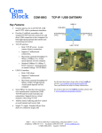
PCMCIA INTERFACE USER MANUAL
1 Scope
The COM-13xx ComBlock modules are PC cards
which support communication with a host computer
through a standard PCMCIA interface. These
ComBlock modules can be used as
(a) ready-to-use application-specific
ComBlocks, or
(b) development platforms with user-developed
code.
This manual addresses both use cases. Its scope is
limited to the 16-bit PCMCIA interface1.
Users of ready-to-use application-specific
ComBlocks should read the following sections:
“Architecture”, “Windows Device Driver
Installation” and on “Applications”.
Developers should also read the sections on
PCMCIA component which implements the
PCMCIA interface within the FPGA
The current implementation is subject to the
following limitations:
• PCMCIA interface with 16-bit memorymapped and 8-bit I/O-mapped data
transfers between ComBlock and host PC
• Windows XP/2000 device driver
Throughput:
The PCMCIA interface sustained (average)
throughput was measured using one-way data
transfer benchmarks as shown below:
Throughput test conditions
Memory-mapped data transfers:
Host computer: AMD processor 1.2 GHz.
C runtime application, no hard disk data
transfers. No other application running.
I/O-mapped data transfers:
Host computer: AMD processor 1.2 GHz.
C runtime application, no hard disk data
transfers. No other application running.
Throughput
9.5 Mbps
(either
direction)
4.5 Mbps
(either
direction)
2 Architecture
The end-to-end communication architecture
between a host computer and the ComBlock
module as a PCMCIA peripheral is illustrated
below:
Java app
API
C/C++
application
.dll
Driver
PC Operating System
PC Hardware
PCMCIA
Component
COM-1300
PCMCIA/CardBus
Development
Platform
1
Software Development environment
Blue: supplied hardware
Green: supplied ready-to-use software
Yellow: application-level code examples.
COM-13xx PC Cards also embody the 32-bit CardBus
interface, as addressed in a separate user manual.
MSS • 18221 Flower Hill Way #A • Gaithersburg, Maryland 20879 • U.S.A.
Telephone: (240) 631-1111 Facsimile: (240) 631-1676 www.comblock.com
© MSS 2000-2005 Issued 9/9/2005
•
2.1 Host side (PC):
In order for a user to setup a PCMCIA connection
between the host computer and the ComBlock, the
user must first create a Java or C/C++ application.
cis_p, iorw_p, memory_p NGC
components for integration within the
VHDL code
The Java application calls simple methods
described in the Java Application Programming
Interface (API) described further in this document.
C/C++ applications can call drivers functions
directly as described in the C/C++ Applications
described further in this document.
2.2 Peripheral side (ComBlock):
On the peripheral side, the PCMCIA connection is
implemented almost entirely within the FPGA as
illustrated below:
to/from PC
Xilinx FPGA
XC3S400
3 Windows Device Driver
Installation
When connecting the COM-1300 PCMCIA
interface for the first time, the user is prompted for
new hardware installation. Follow the step-by-step
instructions shown below each screen shot.
PCMCIA
MicroController
The PCMCIA software package is available in the
ComBlock CD and can also be downloaded from
http://www.comblock.com/download/PCMCIA.zip
32MB
SDRAM
Buffer
40 MHz
Clock
USB
Flash2.0
Controller
Memory
(FPGA
configurations)
40-pin digital I/O
to/from
other
ComBlocks
Development Card Hardware Block Diagram
2.3 Supplied Components:
Click on Next.
The PCMCIA software package provides
software to help users and developers create
PCMCIA communication between the COM-13xx
ComBlock module and a host PC. The software
components include the following:
• Windows device driver for XP/2000 (.sys
and .inf files)
• Java API
• Java simple application code examples
• C/C++ simple application code examples
2
Point to the location where the driver files are and
click OK.
Check “Display a list of known drivers for the
device so that I can choose a specific driver”. Click
“Next”.
Go to the next screen.
Select “Other Devices”. Go to the Next screen.
Click on Next.
The last window for the New Hardware Wizard
should appear, as shown below, for a successfully
installed device.
Click on “Have Disk”.
3
Application examples can be found in the PCMCIA
software package.
5 FPGA/VHDL/DRIVER
Development
This section describes how to create a custom
application that makes use of the PCMCIA medium
on the ComBlock COM-1300 FPGA-based
development platforms. This section can be skipped
by users of ready-to-use application-specific
ComBlock modules.
Click on Finish.
At this point, the driver for COM-1300 with
PCMCIA interface has been successfully installed
and next time the device is plugged in, the system
automatically finds appropriate driver. With the
driver installed, the user can talk to the device,
using the API.
This section focuses primarily on the peripheral
side of the PCMCIA connection.
5.1 Host <-> Target
Communication Methods
4 Applications
In its basic form the PCMCIA component supports
two methods of bi-directional data exchange
between host and target:
4.1 Java API
-
The Java API is documented in
…\Java\API\Pcmcia.html and can be found in the
PCMCIA software package.
One virtual bi-directional channel is I/O
mapped and exchanges 8-bit wide data.
-
The other virtual bi-directional channel is
memory-mapped, exchanges 16-bit words and
is optimized for maximum throughput.
The applications call simple methods to get a
handle, dispose of the handle, read and write.
The DLL, which links the Java application to the
drivers, is provided in the PCMCIA software
package. It is suggested to copy the pcmciaio.dll
file to the Java project directory.
The Java application can transfer data buffers in the
range of 0 to 2,048 Bytes to/from the PCMCIA
target. When addressing a memory-mapped stream,
all transfers are multiple of 2-byte words.
Flow control is implemented by checking the
number of bytes actually transmitted at the end of
the transaction.
The intent is to use the I/O mapped channel to
communicate with ComBlock itself, for monitoring
and control purposes. The Memory-mapped
channel’s intended use is for transferring payload
data.
The addressing scheme is the same for both I/O and
Memory-mapped channels:
- Base address is 0.
- Address range used: 0 - 12
Beyond the basic software, developers can create
multiple I/O and Memory-mapped channels by
instantiating multiple VHDL components and
specifying non-overlapping address ranges.
5.2 Driver Installation
4.2 C/C++ Applications
The applications in C++ contains functions to open
the device handle, send/receive data and close the
handle.
Upon insertion of a COM-1300 (PCMCIA
interface), the bus driver will read the CIS (Card
Information Services), in particular, the vendor ID
and product ID, from the FPGA. Then it searches
4
through the system registries to find matches with
the vendor ID and product ID.
For the first-time installation of COM-1300, the
operating system will discover that the vendor ID
and product ID are new to the system registries. The
user will be directed through a new hardware
installation.
The New Hardware Wizard will check the INF file
in the specified directory to see if it matches the
vendor ID and product ID the host read from the
hardware. If matched, the host will find the required
drivers (.sys) defined in the .inf file, and copies the
drivers to a location described in the .inf file
(C:\WINDOWS\system32\drivers by default).
At this point, the .inf and .sys files will be copied by
the operating system, and the system registry will
be updated to include this device entry. Next time
the device is plugged in, the system automatically
finds it in the registry and links the device to the
appropriate driver.
Note: In case of a conflict of resources with any
other device on a Host PC please modify the
following section in the comblock_pcmcia.inf file:
IOConfig=DF40-DF7F
MemConfig=000DD000-000DD800
The memory or io or both address ranges may need
to be modified to non-conflicting values.
5.3 PCMCIA Component
The PCMCIA implementation on the target side is
encapsulated within three NGC components,
namely, cis_p.ngc, iorw_p.ngc and memory_p.ngc.
This implementation supports two bi-directional
channels:
- One virtual channel that is I/O mapped and
exchanges 8-bit wide data.
- The other virtual channel that is memorymapped, exchanges 16-bit words
Data is exchanged with the PCMCIA component
through a 16Kbit dual-port (elastic) buffer in each
direction.
The PCMCIA component works in conjunction
with the Windows XP/2000 OS drivers and the Java
and C/C++ applications to establish a virtual
channel between the COM-1300 and a host
computer. Only one application can connect to the
PCMCIA at any given time.
5.3.1 Interface
The component is described primarily by its
interface definition:
entity PCMCIA is
port (
--// Clocks, reset
CLK_P: in std_logic;
-- Main processing or I/O clock used outside of this component.
-- All application interface signals are synchronous with CLK_P
-- Key assumptions about speed: CLK_P > 8 MHz
SYNC_RESET: in std_logic;
-- synchronous reset at power up
--// Host bus adapter interface:
-- Note: Pull-ups are defined in the constraint file.
PC_CARD_ADDR: in std_logic_vector(25 downto 0);
-- Address
PC_CARD_DATA: inout std_logic_vector(15 downto 0);
-- Data
PC_CARD_WP_IOIS16_N: out std_logic;
-- WP
During memory only interface
-- IOIS16# During memory or I/O interface
-- PULL-UP
PC_CARD_RESERVED_INPACK_N: out std_logic;
-- RESERVED During memory only interface
-- INPACK# During memory or I/O interface
PC_CARD_BVD2_SPKR_N: out std_logic;
-- BVD2
During memory only interface
-- SPKR#
During memory or I/O interface
-- PULL-UP
PC_CARD_BVD1_STSCHG_N: out std_logic;
-- BVD1
During memory only interface
-- STSCHG# During memory or I/O interface
-- PULL-UP
PC_CARD_RESERVED_IORD_N: in std_logic;
-- RESERVED During memory only interface
-- IORD#
During memory or I/O interface
PC_CARD_RESERVED_IOWR_N: in std_logic;
-- RESERVED During memory only interface
-- IOWR#
During memory or I/O interface
PC_CARD_CE1_N: in std_logic;
-- CE1#
PC_CARD_CE2_N: in std_logic;
-- CE2#
PC_CARD_OE_N: in std_logic;
-- OE#
PC_CARD_WE_N_IN: in std_logic;
-- WE#
PC_CARD_REG_N: in std_logic;
-- REG#
PC_CARD_WAIT_N: out std_logic;
-- WAIT#. Atmel uC to drive WAIT# active low while the FPGA is
-- being configured.
PC_CARD_READY_IREQ_N: out std_logic;
-- READY
During memory only interface
-- IREQ#
During memory or I/O interface
-- PULL-UP
PC_CARD_RESET_UC_MOSI: in std_logic;
-- RESET
During normal microcontroller operation
-- UC_MOSI During microcontroller programming
--// user interfaces
--// Stream1. 16-bit Memory read/write transactions
-- Synchronous with CLK_P clock
5
DATA1_OUT: out std_logic_vector(7 downto 0);
DATA1_OUT_SAMPLE_CLK: out std_logic;
-- read DATA1_OUT at rising edge of CLK_P when
-- DATA1_OUT_SAMPLE_CLK = '1'
-- Note1: the user is responsible for checking
-- DATA1_OUT_BUFFER_EMPTY before
-- reading.
-- Note 2: When the elastic buffer is not empty, DATA1_OUT is
-- present at this interface even before requesting it. The request
-- DATA1_OUT_SAMPLE_CLK_REQ only moves the read pointer
-- to the next read location.
DATA1_OUT_BUFFER_EMPTY: out std_logic;
DATA1_OUT_SAMPLE_CLK_REQ: in std_logic;
-- requests data. If no data is available in the buffer, the
-- DATA1_OUT_SAMPLE_CLK will stay low.
-- (flow control)
Offset
DATA1_IN: in std_logic_vector(7 downto 0);
DATA1_IN_SAMPLE_CLK: in std_logic;
-- read DATA1_IN at rising edge of CLK_P when
-- DATA1_IN_SAMPLE_CLK = '1'
DATA1_IN_SAMPLE_CLK_REQ: out std_logic;
-- requests data when the input elastic buffer is less than half full.
-- (flow control)
--// user interfaces
--// Stream2. 8-bit I/O read/write transactions at I/O address 0
-- Synchronous with CLK_P clock
DATA2_OUT: out std_logic_vector(7 downto 0);
DATA2_OUT_SAMPLE_CLK: out std_logic;
-- read DATA2_OUT at rising edge of CLK_P when
-- DATA2_OUT_SAMPLE_CLK = '1'
-- Note1: the user is responsible for checking –
-- DATA2_OUT_BUFFER_EMPTY before reading.
-- Note 2: When the elastic buffer is not empty, DATA2_OUT is
-- present at this interface even before requesting it. The request –
-- DATA2_OUT_SAMPLE_CLK_REQ
-- only moves the read pointer to the next read location.
DATA2_OUT_BUFFER_EMPTY: out std_logic;
DATA2_OUT_SAMPLE_CLK_REQ: in std_logic;
-- requests data. If no data is available in the buffer, the
-- DATA2_OUT_SAMPLE_CLK will stay low.
-- (flow control)
DATA2_IN: in std_logic_vector(7 downto 0);
DATA2_IN_SAMPLE_CLK: in std_logic;
-- read DATA2_IN at rising edge of CLK_P when
-- DATA2_IN_SAMPLE_CLK = '1'
DATA2_IN_SAMPLE_CLK_REQ: out std_logic
-- requests data when the input elastic buffer is less than half full.
-- (flow control)
--// Test Points
-- Test points are under the shield. 6 at the edge connector.
--TEST_POINTS: out std_logic_vector(6 downto 1)
);
end entity;
5.3.2 Card Information Services
(CIS)
The CIS is a data structure stored in non-volatile
memory within the PC Card. It is read by the
operating system to determine what kind of PC card
is installed, along with its speed, size and the
system resources required by the card.
A detailed description of the PCMCIA CIS is
provided below. The CIS is defined as a ROM
within the VHDL code.
Data
(hex)
Description and interpretation
To
compute
Offset
Address =
Offset * 2
0
1
2
01
03
D4
3
00
4
5
FF
15
6
7
8
9
10
11
12
13
14
15
16
17
18
19
20
21
22
23
24
25
26
27
28
33
34
35
10
04
01
4D
53
53
00
43
4F
4D
20
31
33
30
30
00
FF
20
04
00
00
01
01
1A
05
01
Device info tuple
Link to next tuple
Device Type = Function specific,
WPS = OFF, Speed = 100nS
Memory block size = 1 unit, 512
bytes
End of tuple
Level 1 version / product
information
Link to next tuple
PCMCIA Version 2.x
36
03
37
00
38
39
02
01
40
41
42
1B
16
C1
43
01
M
S
S
End manufacturer name
C
O
M
Space
1
3
0
0
End version information
Tuple termination byte
Manufacturer ID
Link to next tuple
Unregistered PCMCIA ID
Card number & revision
Configuration tuple
Link to next tuple
2-byte (16-bit) configuration
register base address, 1 byte
configuration register mask
Index number of last
configuration entry
Configuration register base
address 0x0200
Configuration register mask.
Enables configuration registers 0
(configuration option register).
Configuration table entry tuple
Link to next tuple
Default bit set, interface bit set,
configuration index 1
Memory or I/O interface
6
44
3D
45
71
46
47
48
B5
1E
66
49
76
50
54
51
E0
52
72
53
5D
54
A6
55
60
56
57
58
00
00
3F
59
50
60
FF
61
FF
62
01
Wait not required for memory
accesses
No write protect.
No ready/busy status needed.
Feature selection field:
IRQ, I/O space, memory, timing,
Vcc power description structures
are present. No Vpp, , misc.
description structures.
Power description structure:
- power down supply current
required
- maximum peak current
required (10 ms average)
- maximum average current (1
second average)
- nominal operating supply
voltage (+/- 5%)
3.3V (3 * 1V + 0.30V extension)
0.30V
6 * 100mA maximum average
current
8 * 100mA maximum peak
current
Power down supply current 5 *
1mA
Timing description structure. A
Wait scale of 1 is defined, a
Ready/Busy scale of 1 is defined,
no reserved time scale is defined.
Wait signal timing descriptor:
7.0 (mantissa) x 100 ns
(exponent) x 1 scaling factor =
700 ns.
Ready/Busy timing descriptor:
5.0 (mantissa) x 100 µs
(exponent) x 1 (scaling factor) =
500 µs max READY delay.
6 I/O address lines, use data bits
D7-D0 to access the registers (8bit wide), specify an I/O range.
Length size descriptor: 1 address
(= 2 bytes) and 1 length (=1
byte). Only one address range
descriptor present.
Start address = 0x00000
memory space.
63
64
00
FF
5.3.3 Synthesis Statistics
The FPGA size occupied by the PCMCIA
component is as follows:
PCMCIA Design Summary:
Logic Utilization:
Number of Slice Flip Flops:
176 out of 7,168 2%
Number of 4 input LUTs:
171 out of 7,168 2%
Logic Distribution:
Number of occupied Slices:
158 out of 3,584 4%
Number of Slices containing only related logic: 158 out
of 158 100%
Number of Slices containing unrelated logic: 0 out of
158 0%
Total Number 4 input LUTs:
249 out of 7,168 3%
Number used as logic:
171
Number used as a route-thru:
78
Number of bonded IOBs:
89 out of 173 51%
IOB Flip Flops:
18
IOB Latches:
16
Number of Block RAMs:
5 out of 16 31%
Number of GCLKs:
1 out of
8 12%
Length of address block = 0x40
(64 bytes)
Interrupt request description
structure: Pulse = 1, Mask = 1,
everything else is 0.
Interrupts: IRQ0, IRQ1, IRQ2,
IRQ3, IRQ4, IRQ5, IRQ6, IRQ7.
Interrupts: IRQ8, IRQ9, IRQ10,
IRQ11, IRQ12, IRQ13, IRQ14,
IRQ15.
Request 256 bytes of common
7
5.4 VHDL code template
A VHDL template project for the COM-1300
PCMCIA/CardBus FPGA development platform is
available on-line at
www.comblock.com/download/com1300template_
001.zip
The template project (-P option) includes:
•
Top-level VHDL source code (.vhd), for
PCMCIA interface.
•
NGC components for cis_p, iorw_p and
memory_p, and the SDRAM driver.
•
the constraint file (.ucf) listing all pin
assignments.
•
The Xilinx project with the synthesis and
implementation settings.
•
The resulting bit files (.mcs) ready to be
loaded into flash memory.
8