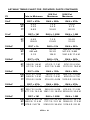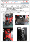
1
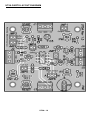
open. The Monostable mode’s Stable State is defined as U1’s Output at pin3 is Low and its Discharge pin at U1 pin 7 is held at ground allowing C2 to discharge or preventing it from charging. The timer will stay in this mode until properly triggered. The discharge path will be from C2 through JMP6 pin2 to pin 1, U1 pin7, to ground through the 555 timer IC, back to C2. When the proper trigger appears at U1 pin2 (Trigger) input the Output at pin3 goes High and the ground at pin7 is removed (unstable state). This allows C2 to start to charge through JMP6 pins 1 to 2, R5, and R4 to VCC. When the charge on C2 reaches the Threshold level (2/3 VCC or Control Voltage if used) U1 pin6 (Threshold) will cause the 555 timer to change to the stable state setting the Output pin (pin3) to a Low and applying ground at the Discharge pin (pin7). The Discharge pin (pin7) being at ground discharges C2. The time C2 charges in the Unstable state is the Pulse Width (PW) of the signal, it can be calculated with the following formula. C2’s discharge path has no resistance so it is considered to be instantaneous. It is important to note that the use of a control voltage will change the Threshold level of the IC; therefore, change the RC timing and the pulse width. PW = 1.1 * C2 * (R4 +R5) Astable Mode: In the Astable (no stable states) mode the timer is free running and acts like a square wave generator. We will call the High output of the square wave from the 555 timer Pulse Width (PW) and the Low portion of the square wave Rest Time (RT). The Pulse width is determined by the RC charge time of the Charging Network and Rest Time is determined by the discharge time of the Charging Network. In Astable mode JMP4 (Input Select) is removed disconnecting the signal inputs. JMP6 is set connecting pin2 and pin3. This sets up C2 charge and discharge path and connect both U1 pin2 and pin6 to C2. Since this mode is free running no input, other than applying power, is needed to start the circuit. Lets start at the end of rest time with U1 pin3 (Output) Low, U1 pin7 (Discharge) grounded, and C2 discharging slowly. When the charge on C2 decreases below the Trigger level (1/3VCC or ½ control voltage if used) U1 pin2 (Trigger input) causes the start of Pulse Width by setting U1 pin3 (Out) to go High and Discharge (pin7) removes ground. C2 is now allowed to charge through R7, R6, R5, R4, to VCC. When C2’s charge reaches Threshold level (2/3 VCC or Control Voltage if used) U1 pin6 (Threshold) ends UT5A 8