1
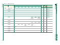
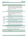
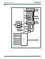
UM10120
Chapter 9: Universal Asynchronous Receiver/Transmitter 0
(UART0)
Rev. 01 — 24 June 2005
User manual
9.1 Features
•
•
•
•
•
16 byte Receive and Transmit FIFOs
Register locations conform to ‘550 industry standard.
Receiver FIFO trigger points at 1, 4, 8, and 14 bytes.
Built-in baud rate generator.
LPC2131/2/4/6/8 UART0 contains mechanism that enables software flow control
implementation.
9.2 Pin description
Table 72:
UART0 pin description
Pin
Type
Description
RXD0
Input
Serial Input. Serial receive data.
TXD0
Output
Serial Output. Serial transmit data.
9.3 Register description
UART0 contains registers organized as shown in Table 73. The Divisor Latch Access Bit
(DLAB) is contained in U0LCR[7] and enables access to the Divisor Latches.
© Koninklijke Philips Electronics N.V. 2005. All rights reserved.
User manual
Rev. 01 — 24 June 2005
84
xxxxxxxxxxxxxxxxxxxxx xxxxxxxxxxxxxxxxxxxxxxxxxx xxxxxxx x x x xxxxxxxxxxxxxxxxxxxxxxxxxxxxxx xxxxxxxxxxxxxxxxxxx xx xx xxxxx
xxxxxxxxxxxxxxxxxxxxxxxxxxx xxxxxxxxxxxxxxxxxxx xxxxxx xxxxxxxxxxxxxxxxxxxxxxxxxxxxxxxxxxx xxxxxxxxxxxx x x
xxxxxxxxxxxxxxxxxxxxx xxxxxxxxxxxxxxxxxxxxxxxxxxxxxx xxxxx xxxxxxxxxxxxxxxxxxxxxxxxxxxxxxxxxxxxxxxxxxxxxxxxxx xxxxxxxx
xxxxxxxxxxxxxxxxxxxxxxxxx xxxxxxxxxxxxxxxxxxxx xxx
Description
Bit functions and addresses
MSB
BIT7
LSB
BIT6
BIT5
BIT4
BIT3
BIT2
BIT1
Access Reset
Address
value[1]
BIT0
Rev. 01 — 24 June 2005
Receiver Buffer
Register
8-bit Read Data
RO
NA
0xE000 C000
(DLAB=0)
U0THR
Transmit Holding
Register
8-bit Write Data
WO
NA
0xE000 C000
(DLAB=0)
U0DLL
Divisor Latch LSB
8-bit Data
R/W
0x01
0xE000 C000
(DLAB=1)
U0DLM
Divisor Latch MSB
8-bit Data
R/W
0x00
0xE000 C004
(DLAB=1)
U0IER
Interrupt Enable
Register
Enable R/W
RX Data
Available
Interrupt
0x00
0xE000 C004
(DLAB=0)
U0IIR
Interrupt ID
Register
U0FCR
FIFO Control
Register
U0LCR
Line Control
Register
DLAB
Set
Break
Stick
Parity
Even
Parity
Select
Parity
Enable
Number
of Stop
Bits
U0LSR
Line Status
Register
RX FIFO
Error
TEMT
THRE
BI
FE
PE
U0SCR
Scratch Pad
Register
U0TER
Transmit Enable
Register
Reserved Reserved Reserved Reserved Reserved
Enable
RX Line
Status
Interrupt
Enable
THRE
Interrupt
IIR2
IIR1
IIR0
RO
0x01
0xE000 C008
RX FIFO
Reset
FIFO
Enable
WO
0x00
0xE000 C008
Word Length Select R/W
0x00
0xE000 C00C
RO
0x60
0xE000 C014
R/W
0x00
0xE000 C01C
Reserved Reserved Reserved Reserved Reserved Reserved Reserved R/W
0x80
0xE000 C030
FIFOs Enabled
[1]
RX Trigger
Reserved Reserved
IIR3
Reserved Reserved Reserved TX FIFO
Reset
OE
8-bit Data
TXEN
DR
Reset value relects the data stored in used bits only. It does not include reserved bits content.
UM10120
Chapter 9: UART0
85
© Koninklijke Philips Electronics N.V. 2005. All rights reserved.
U0RBR
Philips Semiconductors
Name
UART0 register map
Volume 1
User manual
Table 73:
UM10120
Philips Semiconductors
Volume 1
Chapter 9: UART0
9.3.1 UART0 Receiver Buffer Register (U0RBR - 0xE000 C000, when
DLAB = 0, Read Only)
The U0RBR is the top byte of the UART0 Rx FIFO. The top byte of the Rx FIFO contains
the oldest character received and can be read via the bus interface. The LSB (bit 0)
represents the “oldest” received data bit. If the character received is less than 8 bits, the
unused MSBs are padded with zeroes.
The Divisor Latch Access Bit (DLAB) in U0LCR must be zero in order to access the
U0RBR. The U0RBR is always Read Only.
Since PE, FE and BI bits correspond to the byte sitting on the top of the RBR FIFO (i.e.
the one that will be read in the next read from the RBR), the right approach for fetching the
valid pair of received byte and its status bits is first to read the content of the U0LSR
register, and then to read a byte from the U0RBR.
Table 74:
UART0 Receiver Buffer Register (U0RBR - address 0xE000 C000, when DLAB = 0,
Read Only) bit description
Bit
Symbol
Description
Reset value
7:0
RBR
The UART0 Receiver Buffer Register contains the oldest
received byte in the UART0 Rx FIFO.
undefined
9.3.2 UART0 Transmit Holding Register (U0THR - 0xE000 C000, when
DLAB = 0, Write Only)
The U0THR is the top byte of the UART0 TX FIFO. The top byte is the newest character in
the TX FIFO and can be written via the bus interface. The LSB represents the first bit to
transmit.
The Divisor Latch Access Bit (DLAB) in U0LCR must be zero in order to access the
U0THR. The U0THR is always Write Only.
Table 75:
UART0 Transmit Holding Register (U0THR - address 0xE000 C000, when
DLAB = 0, Write Only) bit description
Bit
Symbol
Description
Reset value
7:0
THR
Writing to the UART0 Transmit Holding Register causes the data NA
to be stored in the UART0 transmit FIFO. The byte will be sent
when it reaches the bottom of the FIFO and the transmitter is
available.
9.3.3 UART0 Divisor Latch Registers 0 and 1 (U0DLL - 0xE000 C000 and
U0DLM - 0xE000 C004, when DLAB = 1)
The UART0 Divisor Latch is part of the UART0 Baud Rate Generator and holds the value
used to divide the VPB clock (PCLK) in order to produce the baud rate clock, which must
be 16x the desired baud rate (Equation 1). The U0DLL and U0DLM registers together
form a 16 bit divisor where U0DLL contains the lower 8 bits of the divisor and U0DLM
contains the higher 8 bits of the divisor. A 0x0000 value is treated like a 0x0001 value as
division by zero is not allowed.The Divisor Latch Access Bit (DLAB) in U0LCR must be
one in order to access the UART0 Divisor Latches.
Details on how to select the right value for U0DLL and U0DLM can be found later on in
this chapter.
© Koninklijke Philips Electronics N.V. 2005. All rights reserved.
User manual
Rev. 01 — 24 June 2005
86
UM10120
Philips Semiconductors
Volume 1
Chapter 9: UART0
(1)
pclk
UART0 baudrate = ----------------------------------------------------------------------------16 × ( 16 × U0DLM + U0DLL )
Table 76:
UART0 Divisor Latch LSB register (U0DLL - address 0xE000 C000, when
DLAB = 1) bit description
Bit
Symbol
Description
Reset value
7:0
DLLSB
The UART0 Divisor Latch LSB Register, along with the U0DLM
register, determines the baud rate of the UART0.
0x01
Table 77:
UART0 Divisor Latch MSB register (U0DLM - address 0xE000 C004, when
DLAB = 1) bit description
Bit
Symbol
Description
Reset value
7:0
DLMSB
The UART0 Divisor Latch MSB Register, along with the U0DLL
register, determines the baud rate of the UART0.
0x00
9.3.4 UART0 Baud-rate calculation
Example: Using UART0baudrate Equation 1 from above, it can be determined that system
with PCLK = 20 MHz, U0DL = 130 (U0DLM = 0x00 and U0DLL = 0x82) will enable
UART0 with UART0baudrate=9615 baud.
Table 78:
Some baud-rates available when using 20 MHz peripheral clock (PCLK=20 MHz)
Desired
U0DLM:U0DLL
baud-rate hex
dec
% error[1]
Desired
U0DLM:U0DLL
baud-rate hex
dec
% error[1]
50
0x61A8
25000
0
4800
0x0104
260
0.1603
75
0x411B
16667
0.0020
7200
0x00AE
174
0.2235
110
0x2C64
11364
0.0032
9600
0x0082
130
0.1603
134.5
0x244E
9294
0.0034
19200
0x0041
65
0.1603
150
0x208D
8333
0.0040
38400
0x0021
33
1.3573
300
0x1047
4167
0.0080
56000
0x0021
22
1.4610
600
0x0823
2083
0.0160
57600
0x0016
22
1.3573
1200
0x0412
1042
0.0320
112000
0x000B
11
1.4610
1800
0x02B6
694
0.0640
115200
0x000B
11
1.3573
2000
0x0271
625
0
224000
0x0006
6
6.9940
2400
0x0209
521
0.0320
448000
0x0003
3
6.9940
3600
0x015B
347
0.0640
[1]
Relative error calculated as: actual_baudrate/desired_baudrate-1. Actual baudrate based on Equation 1.
9.3.5 UART0 Interrupt Enable Register (U0IER - 0xE000 C004, when
DLAB = 0)
The U0IER is used to enable the three UART0 interrupt sources.
© Koninklijke Philips Electronics N.V. 2005. All rights reserved.
User manual
Rev. 01 — 24 June 2005
87
UM10120
Philips Semiconductors
Volume 1
Chapter 9: UART0
Table 79:
UART0 Interrupt Enable Register (U0IER - address 0xE000 C004, when DLAB = 0)
bit description
Bit
Symbol
0
RBR
Interrupt
Enable
1
2
7:3
THRE
Interrupt
Enable
Value
Description
Reset
value
U0IER[0] enables the Receive Data Available interrupt
for UART0. It also controls the Character Receive
Time-out interrupt.
0
0
Disable the RDA interrupts.
1
Enable the RDA interrupts.
U0IER[1] enables the THRE interrupt for UART0. The
status of this can be read from U0LSR[5].
0
Disable the THRE interrupts.
1
Enable the THRE interrupts.
RX Line
Status
Interrupt
Enable
0
U0IER[2] enables the UART0 RX line status interrupts.
0
The status of this interrupt can be read from U0LSR[4:1].
0
Disable the RX line status interrupts.
1
Enable the RX line status interrupts.
-
Reserved, user software should not write ones to
reserved bits. The value read from a reserved bit is not
defined.
NA
9.3.6 UART0 Interrupt Identification Register (U0IIR - 0xE000 C008, Read
Only)
The U0IIR provides a status code that denotes the priority and source of a pending
interrupt. The interrupts are frozen during an U0IIR access. If an interrupt occurs during
an U0IIR access, the interrupt is recorded for the next U0IIR access.
Table 80:
UART0 Interrupt Identification Register (UOIIR - address 0xE000 C008, read only)
bit description
Bit
Symbol
0
Interrupt
Pending
3:1
Value
Description
Reset
value
Note that U0IIR[0] is active low. The pending interrupt can
be determined by evaluating U0IIR[3:1].
1
0
At least one interrupt is pending.
1
No pending interrupts.
Interrupt
Identification
U0IER[3:1] identifies an interrupt corresponding to the
UART0 Rx FIFO. All other combinations of U0IER[3:1] not
listed above are reserved (000,100,101,111).
011
1 - Receive Line Status (RLS).
010
2a - Receive Data Available (RDA).
110
2b - Character Time-out Indicator (CTI).
001
3 - THRE Interrupt
0
5:4
-
Reserved, user software should not write ones to reserved
bits. The value read from a reserved bit is not defined.
NA
7:6
FIFO Enable
These bits are equivalent to U0FCR[0].
0
© Koninklijke Philips Electronics N.V. 2005. All rights reserved.
User manual
Rev. 01 — 24 June 2005
88
UM10120
Philips Semiconductors
Volume 1
Chapter 9: UART0
Interrupts are handled as described in Table 81. Given the status of U0IIR[3:0], an
interrupt handler routine can determine the cause of the interrupt and how to clear the
active interrupt. The U0IIR must be read in order to clear the interrupt prior to exiting the
Interrupt Service Routine.
The UART0 RLS interrupt (U0IIR[3:1] = 011) is the highest priority interrupt and is set
whenever any one of four error conditions occur on the UART0 Rx input: overrun error
(OE), parity error (PE), framing error (FE) and break interrupt (BI). The UART0 Rx error
condition that set the interrupt can be observed via U0LSR[4:1]. The interrupt is cleared
upon an U0LSR read.
The UART0 RDA interrupt (U0IIR[3:1] = 010) shares the second level priority with the CTI
interrupt (U0IIR[3:1] = 110). The RDA is activated when the UART0 Rx FIFO reaches the
trigger level defined in U0FCR[7:6] and is reset when the UART0 Rx FIFO depth falls
below the trigger level. When the RDA interrupt goes active, the CPU can read a block of
data defined by the trigger level.
The CTI interrupt (U0IIR[3:1] = 110) is a second level interrupt and is set when the UART0
Rx FIFO contains at least one character and no UART0 Rx FIFO activity has occurred in
3.5 to 4.5 character times. Any UART0 Rx FIFO activity (read or write of UART0 RSR) will
clear the interrupt. This interrupt is intended to flush the UART0 RBR after a message has
been received that is not a multiple of the trigger level size. For example, if a peripheral
wished to send a 105 character message and the trigger level was 10 characters, the CPU
would receive 10 RDA interrupts resulting in the transfer of 100 characters and 1 to 5 CTI
interrupts (depending on the service routine) resulting in the transfer of the remaining 5
characters.
Table 81:
UART0 interrupt handling
U0IIR[3:0] Priority Interrupt Type
value[1]
Interrupt Source
0001
None
None
-
Interrupt Reset
-
0110
Highest
RX Line Status / Error
OE[2]
0100
Second
RX Data Available
Rx data available or trigger level reached in FIFO
(U0FCR0=1)
U0RBR Read[3] or
UART0 FIFO drops
below trigger level
1100
Second
Character Time-out
indication
Minimum of one character in the Rx FIFO and no
character input or removed during a time period
depending on how many characters are in FIFO
and what the trigger level is set at (3.5 to 4.5
character times).
U0RBR Read[3]
or
PE[2]
or
FE[2]
or
BI[2]
U0LSR Read[2]
The exact time will be:
[(word length) × 7 − 2] × 8 + [(trigger level −
number of characters) × 8 + 1] RCLKs
0010
Third
THRE
THRE[2]
U0IIR Read (if source of
interrupt) or THR write[4]
[1]
Values "0000", “0011”, “0101”, “0111”, “1000”, “1001”, “1010”, “1011”,”1101”,”1110”,”1111” are reserved.
[2]
For details see Section 9.3.9 “UART0 Line Status Register (U0LSR - 0xE000 C014, Read Only)”
[3]
For details see Section 9.3.1 “UART0 Receiver Buffer Register (U0RBR - 0xE000 C000, when DLAB = 0,
Read Only)”
[4]
For details see Section 9.3.6 “UART0 Interrupt Identification Register (U0IIR - 0xE000 C008, Read Only)”
and Section 9.3.2 “UART0 Transmit Holding Register (U0THR - 0xE000 C000, when DLAB = 0, Write
Only)”
© Koninklijke Philips Electronics N.V. 2005. All rights reserved.
User manual
Rev. 01 — 24 June 2005
89
UM10120
Philips Semiconductors
Volume 1
Chapter 9: UART0
The UART0 THRE interrupt (U0IIR[3:1] = 001) is a third level interrupt and is activated
when the UART0 THR FIFO is empty provided certain initialization conditions have been
met. These initialization conditions are intended to give the UART0 THR FIFO a chance to
fill up with data to eliminate many THRE interrupts from occurring at system start-up. The
initialization conditions implement a one character delay minus the stop bit whenever
THRE=1 and there have not been at least two characters in the U0THR at one time since
the last THRE = 1 event. This delay is provided to give the CPU time to write data to
U0THR without a THRE interrupt to decode and service. A THRE interrupt is set
immediately if the UART0 THR FIFO has held two or more characters at one time and
currently, the U0THR is empty. The THRE interrupt is reset when a U0THR write occurs or
a read of the U0IIR occurs and the THRE is the highest interrupt (U0IIR[3:1] = 001).
9.3.7 UART0 FIFO Control Register (U0FCR - 0xE000 C008)
The U0FCR controls the operation of the UART0 Rx and TX FIFOs.
Table 82:
UART0 FIFO Control Register (U0FCR - address 0xE000 C008) bit description
Bit
Symbol
0
FIFO Enable 0
Value
Description
Reset value
UART0 FIFOs are disabled. Must not be used in the 0
application.
1
Active high enable for both UART0 Rx and TX
FIFOs and U0FCR[7:1] access. This bit must be set
for proper UART0 operation. Any transition on this
bit will automatically clear the UART0 FIFOs.
RX FIFO
Reset
0
No impact on either of UART0 FIFOs.
1
Writing a logic 1 to U0FCR[1] will clear all bytes in
UART0 Rx FIFO and reset the pointer logic. This bit
is self-clearing.
TX FIFO
Reset
0
No impact on either of UART0 FIFOs.
1
Writing a logic 1 to U0FCR[2] will clear all bytes in
UART0 TX FIFO and reset the pointer logic. This bit
is self-clearing.
5:3
-
0
Reserved, user software should not write ones to
reserved bits. The value read from a reserved bit is
not defined.
NA
7:6
RX Trigger
Level
These two bits determine how many receiver
UART0 FIFO characters must be written before an
interrupt is activated.
0
1
2
00
0
0
Trigger level 0 (1 character or 0x01)
01
Trigger level 1 (4 characters or 0x04)
10
Trigger level 2 (8 characters or 0x08)
11
Trigger level 3 (14 characters or 0x0E)
9.3.8 UART0 Line Control Register (U0LCR - 0xE000 C00C)
The U0LCR determines the format of the data character that is to be transmitted or
received.
© Koninklijke Philips Electronics N.V. 2005. All rights reserved.
User manual
Rev. 01 — 24 June 2005
90
UM10120
Philips Semiconductors
Volume 1
Table 83:
Chapter 9: UART0
UART0 Line Control Register (U0LCR - address 0xE000 C00C) bit description
Bit
Symbol
Value
Description
Reset value
1:0
Word Length
Select
00
5 bit character length
0
01
6 bit character length
10
7 bit character length
11
8 bit character length
0
1 stop bit.
1
2 stop bits (1.5 if U0LCR[1:0]=00).
0
Disable parity generation and checking.
1
Enable parity generation and checking.
00
Odd parity. Number of 1s in the transmitted character and the
attached parity bit will be odd.
01
Even Parity. Number of 1s in the transmitted character and the
attached parity bit will be even.
10
Forced "1" stick parity.
11
Forced "0" stick parity.
0
Disable break transmission.
1
Enable break transmission. Output pin UART0 TXD is forced to
logic 0 when U0LCR[6] is active high.
2
3
5:4
6
7
Stop Bit Select
Parity Enable
Parity Select
Break Control
Divisor Latch
0
Access Bit (DLAB) 1
0
0
0
0
Disable access to Divisor Latches.
0
Enable access to Divisor Latches.
9.3.9 UART0 Line Status Register (U0LSR - 0xE000 C014, Read Only)
The U0LSR is a read-only register that provides status information on the UART0 TX and
RX blocks.
Table 84:
UART0 Line Status Register (U0LSR - address 0xE000 C014, read only) bit description
Bit Symbol
0
1
2
Receiver Data
Ready
(RDR)
Value Description
Reset value
U0LSR0 is set when the U0RBR holds an unread character and is cleared
when the UART0 RBR FIFO is empty.
0
U0RBR is empty.
1
U0RBR contains valid data.
Overrun Error
(OE)
0
The overrun error condition is set as soon as it occurs. An U0LSR read clears 0
U0LSR1. U0LSR1 is set when UART0 RSR has a new character assembled
and the UART0 RBR FIFO is full. In this case, the UART0 RBR FIFO will not
be overwritten and the character in the UART0 RSR will be lost.
0
Overrun error status is inactive.
1
Overrun error status is active.
Parity Error
(PE)
When the parity bit of a received character is in the wrong state, a parity error 0
occurs. An U0LSR read clears U0LSR[2]. Time of parity error detection is
dependent on U0FCR[0].
Note: A parity error is associated with the character at the top of the UART0
RBR FIFO.
0
Parity error status is inactive.
1
Parity error status is active.
© Koninklijke Philips Electronics N.V. 2005. All rights reserved.
User manual
Rev. 01 — 24 June 2005
91
UM10120
Philips Semiconductors
Volume 1
Table 84:
UART0 Line Status Register (U0LSR - address 0xE000 C014, read only) bit description
Bit Symbol
3
Chapter 9: UART0
Value Description
Framing Error
(FE)
Reset value
When the stop bit of a received character is a logic 0, a framing error occurs. 0
An U0LSR read clears U0LSR[3]. The time of the framing error detection is
dependent on U0FCR0. Upon detection of a framing error, the Rx will attempt
to resynchronize to the data and assume that the bad stop bit is actually an
early start bit. However, it cannot be assumed that the next received byte will
be correct even if there is no Framing Error.
Note: A framing error is associated with the character at the top of the UART0
RBR FIFO.
4
0
Framing error status is inactive.
1
Framing error status is active.
Break Interrupt
(BI)
When RXD0 is held in the spacing state (all 0’s) for one full character
0
transmission (start, data, parity, stop), a break interrupt occurs. Once the
break condition has been detected, the receiver goes idle until RXD0 goes to
marking state (all 1’s). An U0LSR read clears this status bit. The time of break
detection is dependent on U0FCR[0].
Note: The break interrupt is associated with the character at the top of the
UART0 RBR FIFO.
5
6
7
Transmitter
Holding
Register Empty
(THRE))
Transmitter
Empty
(TEMT)
0
Break interrupt status is inactive.
1
Break interrupt status is active.
THRE is set immediately upon detection of an empty UART0 THR and is
cleared on a U0THR write.
0
U0THR contains valid data.
1
U0THR is empty.
1
TEMT is set when both U0THR and U0TSR are empty; TEMT is cleared when 1
either the U0TSR or the U0THR contain valid data.
0
U0THR and/or the U0TSR contains valid data.
1
U0THR and the U0TSR are empty.
Error in RX
FIFO
(RXFE)
U0LSR[7] is set when a character with a Rx error such as framing error, parity 0
error or break interrupt, is loaded into the U0RBR. This bit is cleared when the
U0LSR register is read and there are no subsequent errors in the UART0
FIFO.
0
U0RBR contains no UART0 RX errors or U0FCR[0]=0.
1
UART0 RBR contains at least one UART0 RX error.
9.3.10 UART0 Scratch pad register (U0SCR - 0xE000 C01C)
The U0SCR has no effect on the UART0 operation. This register can be written and/or
read at user’s discretion. There is no provision in the interrupt interface that would indicate
to the host that a read or write of the U0SCR has occurred.
Table 85:
UART0 Scratch pad register (U0SCR - address 0xE000 C01C) bit description
Bit
Symbol
Description
Reset value
7:0
Pad
A readable, writable byte.
0x00
© Koninklijke Philips Electronics N.V. 2005. All rights reserved.
User manual
Rev. 01 — 24 June 2005
92
UM10120
Philips Semiconductors
Volume 1
Chapter 9: UART0
9.3.11 UART0 Transmit Enable Register (U0TER - 0xE000 C030)
LPC2131/2/4/6/8’s U0TER enables implementation of software flow control. When
TXEn=1, UART0 transmitter will keep sending data as long as they are available. As soon
as TXEn becomes 0, UART0 transmittion will stop.
Table 86 describes how to use TXEn bit in order to achieve software flow control.
Table 86:
UART0 Transmit Enable Register (U0TER - address 0xE000 C030) bit description
Bit
Symbol
Description
Reset
value
6:0
-
Reserved, user software should not write ones to reserved bits. The
value read from a reserved bit is not defined.
NA
7
TXEN
When this bit is 1, as it is after a Reset, data written to the THR is output 1
on the TXD pin as soon as any preceding data has been sent. If this bit
is cleared to 0 while a character is being sent, the transmission of that
character is completed, but no further characters are sent until this bit is
set again. In other words, a 0 in this bit blocks the transfer of characters
from the THR or TX FIFO into the transmit shift register. Software
implementing software-handshaking can clear this bit when it receives
an XOFF character (DC3). Software can set this bit again when it
receives an XON (DC1) character.
9.4 Architecture
The architecture of the UART0 is shown below in the block diagram.
The VPB interface provides a communications link between the CPU or host and the
UART0.
The UART0 receiver block, U0RX, monitors the serial input line, RXD0, for valid input. The
UART0 RX Shift Register (U0RSR) accepts valid characters via RXD0. After a valid
character is assembled in the U0RSR, it is passed to the UART0 RX Buffer Register FIFO
to await access by the CPU or host via the generic host interface.
The UART0 transmitter block, U0TX, accepts data written by the CPU or host and buffers
the data in the UART0 TX Holding Register FIFO (U0THR). The UART0 TX Shift Register
(U0TSR) reads the data stored in the U0THR and assembles the data to transmit via the
serial output pin, TXD0.
The UART0 Baud Rate Generator block, U0BRG, generates the timing enables used by
the UART0 TX block. The U0BRG clock input source is the VPB clock (PCLK). The main
clock is divided down per the divisor specified in the U0DLL and U0DLM registers. This
divided down clock is a 16x oversample clock, NBAUDOUT.
The interrupt interface contains registers U0IER and U0IIR. The interrupt interface
receives several one clock wide enables from the U0TX and U0RX blocks.
Status information from the U0TX and U0RX is stored in the U0LSR. Control information
for the U0TX and U0RX is stored in the U0LCR.
© Koninklijke Philips Electronics N.V. 2005. All rights reserved.
User manual
Rev. 01 — 24 June 2005
93
UM10120
Philips Semiconductors
Volume 1
Chapter 9: UART0
U0TX
U0THR
NTXRDY
U0TSR
TXD0
U0BRG
U0DLL
NBAUDOUT
U0DLM
RCLK
U0RX
NRXRDY
INTERRUPT
U0RBR
U0INTR
U0RSR
RXD0
U0IER
U0IIR
U0FCR
U0LSR
U0SCR
U0LCR
PA[2:0]
PSEL
PSTB
PWRITE
PD[7:0]
VPB
INTERFACE
DDIS
AR
MR
PCLK
Fig 18. LPC2131/2/4/6/8 UART0 block diagram
© Koninklijke Philips Electronics N.V. 2005. All rights reserved.
User manual
Rev. 01 — 24 June 2005
94