1
eZ80F92 Development Kit
User Manual
PRELIMINARY
UM013904-0203
ZiLOG Worldwide Headquarters • 532 Race Street • San Jose, CA 95126
Telephone: 408.558.8500 • Fax: 408.558.8300 • www.ZiLOG.com
eZ80F92 Development Kit
User Manual
ii
This publication is subject to replacement by a later edition. To determine whether a later
edition exists, or to request copies of publications, contact:
ZiLOG Worldwide Headquarters
532 Race Street
San Jose, CA 95126
Telephone: 408.558.8500
Fax: 408.558.8300
www.zilog.com
Document Disclaimer
ZiLOG is a registered trademark of ZiLOG Inc. in the United States and in other countries. All other products
and/or service names mentioned herein may be trademarks of the companies with which they are associated.
©2003 by ZiLOG, Inc. All rights reserved. Information in this publication concerning the devices,
applications, or technology described is intended to suggest possible uses and may be superseded. ZiLOG,
INC. DOES NOT ASSUME LIABILITY FOR OR PROVIDE A REPRESENTATION OF ACCURACY OF
THE INFORMATION, DEVICES, OR TECHNOLOGY DESCRIBED IN THIS DOCUMENT. ZiLOG
ALSO DOES NOT ASSUME LIABILITY FOR INTELLECTUAL PROPERTY INFRINGEMENT
RELATED IN ANY MANNER TO USE OF INFORMATION, DEVICES, OR TECHNOLOGY
DESCRIBED HEREIN OR OTHERWISE. Except with the express written approval of ZiLOG, use of
information, devices, or technology as critical components of life support systems is not authorized. No
licenses are conveyed, implicitly or otherwise, by this document under any intellectual property rights.
PRELIMINARY
UM013904-0203
eZ80F92 Development Kit
User Manual
iii
Safeguards
The following precautions must be observed when working with the
devices described in this document.
Caution: Always use a grounding strap to prevent damage resulting from
electrostatic discharge (ESD).
UM013904-0203
PRELIMINARY
Safeguards
eZ80F92 Development Kit
User Manual
iv
PRELIMINARY
UM013904-0203
eZ80F92 Development Kit
User Manual
v
Table of Contents
Safeguards . . . . . . . . . . . . . . . . . . . . . . . . . . . . . . . . . . . . . . . . . . . . . . . . . . .iii
List of Figures . . . . . . . . . . . . . . . . . . . . . . . . . . . . . . . . . . . . . . . . . . . . . . . vii
List of Tables . . . . . . . . . . . . . . . . . . . . . . . . . . . . . . . . . . . . . . . . . . . . . . . . . ix
Introduction . . . . . . . . . . . . . . . . . . . . . . . . . . . . . . . . . . . . . . . . . . . . . . . . . . 1
Kit Features . . . . . . . . . . . . . . . . . . . . . . . . . . . . . . . . . . . . . . . . . . . . . . . 1
Hardware Specifications . . . . . . . . . . . . . . . . . . . . . . . . . . . . . . . . . . 2
eZ80® Development Platform Overview . . . . . . . . . . . . . . . . . . . . . . . . 3
eZ80® Development Platform . . . . . . . . . . . . . . . . . . . . . . . . . . . . . . . . . . . . 7
Functional Description . . . . . . . . . . . . . . . . . . . . . . . . . . . . . . . . . . . . . . 7
Physical Dimensions . . . . . . . . . . . . . . . . . . . . . . . . . . . . . . . . . . . . 9
Operational Description . . . . . . . . . . . . . . . . . . . . . . . . . . . . . . . . . . . . 10
eZ80F92 Flash Module Interface . . . . . . . . . . . . . . . . . . . . . . . . . . 10
Application Module Interface . . . . . . . . . . . . . . . . . . . . . . . . . . . . 20
I/O Functionality . . . . . . . . . . . . . . . . . . . . . . . . . . . . . . . . . . . . . . 23
Embedded Modem Socket Interface . . . . . . . . . . . . . . . . . . . . . . . 28
eZ80® Development Platform Memory . . . . . . . . . . . . . . . . . . . . . 30
LEDs . . . . . . . . . . . . . . . . . . . . . . . . . . . . . . . . . . . . . . . . . . . . . . . . 33
Push Buttons . . . . . . . . . . . . . . . . . . . . . . . . . . . . . . . . . . . . . . . . . . 33
Jumpers . . . . . . . . . . . . . . . . . . . . . . . . . . . . . . . . . . . . . . . . . . . . . . 34
Connectors . . . . . . . . . . . . . . . . . . . . . . . . . . . . . . . . . . . . . . . . . . . 39
Console . . . . . . . . . . . . . . . . . . . . . . . . . . . . . . . . . . . . . . . . . . . . . . 40
Modem . . . . . . . . . . . . . . . . . . . . . . . . . . . . . . . . . . . . . . . . . . . . . . 40
I2C Devices . . . . . . . . . . . . . . . . . . . . . . . . . . . . . . . . . . . . . . . . . . . . . . 40
DC Characteristics . . . . . . . . . . . . . . . . . . . . . . . . . . . . . . . . . . . . . . . . 41
eZ80F92 Flash Module . . . . . . . . . . . . . . . . . . . . . . . . . . . . . . . . . . . . . . . . 43
Functional Description . . . . . . . . . . . . . . . . . . . . . . . . . . . . . . . . . . . . . 43
Physical Dimensions . . . . . . . . . . . . . . . . . . . . . . . . . . . . . . . . . . . 44
Operational Description . . . . . . . . . . . . . . . . . . . . . . . . . . . . . . . . . . . . 47
UM013904-0203
PRELIMINARY
Table of Contents
eZ80F92 Development Kit
User Manual
vi
eZ80F92 Flash Module Memory . . . . . . . . . . . . . . . . . . . . . . . . . . 47
Reset Generator . . . . . . . . . . . . . . . . . . . . . . . . . . . . . . . . . . . . . . . . 48
IrDA Transceiver . . . . . . . . . . . . . . . . . . . . . . . . . . . . . . . . . . . . . . 48
DC Characteristics . . . . . . . . . . . . . . . . . . . . . . . . . . . . . . . . . . . . . . . . . 51
Flash Loader Utility . . . . . . . . . . . . . . . . . . . . . . . . . . . . . . . . . . . . . . . . 51
Mounting the Module . . . . . . . . . . . . . . . . . . . . . . . . . . . . . . . . . . . . . . 51
Changing the Power Supply Plug . . . . . . . . . . . . . . . . . . . . . . . . . . . . . 52
ZPAKII . . . . . . . . . . . . . . . . . . . . . . . . . . . . . . . . . . . . . . . . . . . . . . . . . . . . . 54
ZDI Target Interface Module . . . . . . . . . . . . . . . . . . . . . . . . . . . . . . . . 54
JTAG . . . . . . . . . . . . . . . . . . . . . . . . . . . . . . . . . . . . . . . . . . . . . . . . . . . 54
Application Modules . . . . . . . . . . . . . . . . . . . . . . . . . . . . . . . . . . . . . . . 54
ZDSII . . . . . . . . . . . . . . . . . . . . . . . . . . . . . . . . . . . . . . . . . . . . . . . . . . . . . . 56
Troubleshooting . . . . . . . . . . . . . . . . . . . . . . . . . . . . . . . . . . . . . . . . . . . . . . 57
Overview . . . . . . . . . . . . . . . . . . . . . . . . . . . . . . . . . . . . . . . . . . . . . . . . 57
Cannot Download Code . . . . . . . . . . . . . . . . . . . . . . . . . . . . . . . . . . . . 57
No Output on Console Port . . . . . . . . . . . . . . . . . . . . . . . . . . . . . . . . . . 57
IrDA Port Not Working . . . . . . . . . . . . . . . . . . . . . . . . . . . . . . . . . . . . . 58
Contacting ZiLOG Customer Support . . . . . . . . . . . . . . . . . . . . . . . . . 58
Schematic Diagrams . . . . . . . . . . . . . . . . . . . . . . . . . . . . . . . . . . . . . . . . . . . 59
eZ80® Development Platform . . . . . . . . . . . . . . . . . . . . . . . . . . . . 59
eZ80F92 Flash Module . . . . . . . . . . . . . . . . . . . . . . . . . . . . . . . . . . 64
Appendix A. . . . . . . . . . . . . . . . . . . . . . . . . . . . . . . . . . . . . . . . . . . . . . . . . . 73
General Array Logic Equations . . . . . . . . . . . . . . . . . . . . . . . . . . . . . . . 73
U10 Address Decoder . . . . . . . . . . . . . . . . . . . . . . . . . . . . . . . . . . . 73
U15 Address Decoder . . . . . . . . . . . . . . . . . . . . . . . . . . . . . . . . . . . 76
Customer Feedback Form . . . . . . . . . . . . . . . . . . . . . . . . . . . . . . . . . . . . . . . 79
Table of Contents
PRELIMINARY
UM013904-0203
eZ80F92 Development Kit
User Manual
vii
List of Figures
Figure 1.
Figure 2.
Figure 3.
Figure 4.
Figure 5.
Figure 6.
Figure 7.
Figure 8.
Figure 9.
Figure 10.
Figure 11.
Figure 12.
Figure 13.
Figure 14.
Figure 15.
Figure 16.
Figure 17.
Figure 18.
Figure 19.
Figure 20.
UM013904-0203
eZ80® Development Platform Block Diagram with
eZ80F92 Flash Module . . . . . . . . . . . . . . . . . . . . . . . . . . . . 4
The eZ80® Development Platform . . . . . . . . . . . . . . . . . . . 5
The eZ80F92 Flash Module . . . . . . . . . . . . . . . . . . . . . . . . 6
Basic eZ80® Development Platform Block Diagram . . . . . 8
Physical Dimensions of the eZ80® Development Platform 9
eZ80® Development Platform Peripheral Bus Connector
Pin Configuration—JP1 . . . . . . . . . . . . . . . . . . . . . . . . . . 11
eZ80® Development Platform I/O Connector Pin
Configuration—JP2 . . . . . . . . . . . . . . . . . . . . . . . . . . . . . . 16
Trigger Pins J21 and J22 . . . . . . . . . . . . . . . . . . . . . . . . . . 27
Embedded Modem Socket Interface—J1, J5, and J9 . . . . 28
Memory Map of the eZ80® Development Platform and
eZ80F92 Flash Module . . . . . . . . . . . . . . . . . . . . . . . . . . . 32
Physical Dimensions of the eZ80F92 Flash Module . . . . 44
eZ80F92 Flash Module—Top Layer . . . . . . . . . . . . . . . . . 45
eZ80F92 Flash Module—Bottom Layer . . . . . . . . . . . . . . 46
IrDA Hardware Connections . . . . . . . . . . . . . . . . . . . . . . . 49
9VDC Universal Power Supply Components . . . . . . . . . . 52
Inserting a New Plug Configuration . . . . . . . . . . . . . . . . . 53
eZ80® Development Platform Schematic Diagram,
#1 of 5 . . . . . . . . . . . . . . . . . . . . . . . . . . . . . . . . . . . . . . . . 59
eZ80® Development Platform Schematic Diagram,
#2 of 5 . . . . . . . . . . . . . . . . . . . . . . . . . . . . . . . . . . . . . . . . 60
eZ80® Development Platform Schematic Diagram,
#3 of 5 . . . . . . . . . . . . . . . . . . . . . . . . . . . . . . . . . . . . . . . . 61
eZ80® Development Platform Schematic Diagram,
#4 of 5 . . . . . . . . . . . . . . . . . . . . . . . . . . . . . . . . . . . . . . . . 62
PRELIMINARY
List of Figures
eZ80F92 Development Kit
User Manual
viii
Figure 21. eZ80® Development Platform Schematic Diagram,
#5 of 5—RS-485 Cable . . . . . . . . . . . . . . . . . . . . . . . . . . . 63
Figure 22. Schematic Diagram, #1 of 9—Top Level . . . . . . . . . . . . . 64
Figure 23. Schematic Diagram, #2 of 9—100-Pin QFP eZ80F92
Device . . . . . . . . . . . . . . . . . . . . . . . . . . . . . . . . . . . . . . . . 65
Figure 24. Schematic Diagram, #3 of 9—36-Pin SRAM Device . . . . 66
Figure 25. Schematic Diagram, #4 of 9—NOR Flash Device . . . . . . 67
Figure 26. Schematic Diagram, #5 of 9—eZ80F92 Flash Module . . . 68
Figure 27. Schematic Diagram, #6 of 9—IrDA Reset . . . . . . . . . . . . 69
Figure 28. Schematic Diagram, #7 of 9—Headers . . . . . . . . . . . . . . . 70
Figure 29. Schematic Diagram, #8 of 9—Power Supply . . . . . . . . . . 71
Figure 30. Schematic Diagram, #9 of 9—Control Logic . . . . . . . . . . 72
List of Figures
PRELIMINARY
UM013904-0203
eZ80F92 Development Kit
User Manual
ix
List of Tables
Table 1.
Table 2.
Table 3.
Table 4.
Table 5.
Table 6.
Table 7.
Table 8.
Table 9.
Table 10.
Table 11.
Table 12.
Table 13.
Table 14.
Table 15.
Table 16.
Table 17.
Table 18.
Table 19.
Table 20.
Table 21.
Table 22.
Table 23.
Table 24.
UM013904-0203
eZ80® Development Platform Hardware Specifications . . 2
eZ80® Development Platform Peripheral Bus Connector
Identification—JP1 . . . . . . . . . . . . . . . . . . . . . . . . . . . . . . 12
eZ80® Development Platform I/O Connector
Identification—JP2 . . . . . . . . . . . . . . . . . . . . . . . . . . . . . . 17
GPIO Connector J6 . . . . . . . . . . . . . . . . . . . . . . . . . . . . . . 21
CPU Bus Connector J8 . . . . . . . . . . . . . . . . . . . . . . . . . . . 23
LED and Port Emulation Addresses . . . . . . . . . . . . . . . . . 24
LED Anode/GPIO Port A Output Control Register . . . . . 24
GPIO Data Register . . . . . . . . . . . . . . . . . . . . . . . . . . . . . . 25
Bit Access to the LED Cathode, Modem, and Triggers . . 26
Connector J5 . . . . . . . . . . . . . . . . . . . . . . . . . . . . . . . . . . . 28
Connector J9 . . . . . . . . . . . . . . . . . . . . . . . . . . . . . . . . . . . 29
Connector J1 . . . . . . . . . . . . . . . . . . . . . . . . . . . . . . . . . . . 29
J2—DIS_IrDA . . . . . . . . . . . . . . . . . . . . . . . . . . . . . . . . . 34
J3—DIS_EM . . . . . . . . . . . . . . . . . . . . . . . . . . . . . . . . . . . 35
J7—FlashWE (Off-Chip) . . . . . . . . . . . . . . . . . . . . . . . . . 35
J11—DIS_Flash (Off-Chip) . . . . . . . . . . . . . . . . . . . . . . . 36
J12—5VDC/3.3VDC for an Embedded Modem . . . . . . . 36
J14—RI . . . . . . . . . . . . . . . . . . . . . . . . . . . . . . . . . . . . . . . 37
J15—RS485_1_EN . . . . . . . . . . . . . . . . . . . . . . . . . . . . . . 37
J16—RS485_2_EN . . . . . . . . . . . . . . . . . . . . . . . . . . . . . . 38
J17—RT_1 . . . . . . . . . . . . . . . . . . . . . . . . . . . . . . . . . . . . 38
J18—RT_2 . . . . . . . . . . . . . . . . . . . . . . . . . . . . . . . . . . . . 39
I2C Addresses . . . . . . . . . . . . . . . . . . . . . . . . . . . . . . . . . . 40
DC Current Characteristics of the eZ80® Development
Platform with Different Module Loads . . . . . . . . . . . . . . . 41
PRELIMINARY
List of Tables
eZ80F92 Development Kit
User Manual
x
List of Tables
PRELIMINARY
UM013904-0203
eZ80F92 Development Kit
User Manual
1
Introduction
The eZ80F92 Development Kit provides a general-purpose platform for
evaluating the capabilities and operation of ZiLOG’s eZ80F92 microcontroller. The eZ80F92 is a member of ZiLOG’s eZ80Acclaim! product
line, which offers on-chip Flash capability. The eZ80F92 Development
Kit features two primary boards: the eZ80® Development Platform and
the eZ80F92 Flash Module. This arrangement provides a full development platform when using both boards. It can also provide a smaller-sized
reference platform with the eZ80F92 Flash Module as a stand-alone
development tool.1
Kit Features
The key features of the eZ80F92 Development Kit are:
•
eZ80® Development Platform:
– Up to 2MB fast SRAM (12ns access time; 1MB factoryinstalled, with 512KB on module, 512KB on platform)
– Embedded modem socket with a U.S. telephone line interface
–
I2C EEPROM
–
–
I2C configuration register
GPIO, logic circuit, and memory headers
–
Supported by ZiLOG Developer Studio II and the eZ80® CCompiler
LEDs, including a 7x5 LED matrix
Platform configuration jumpers
–
–
1. Other members of the eZ80Acclaim! product line include the eZ80F91 and eZ80F93 microcontrollers. A scaled-down eZ80F92 Ethernet Module is also available. Contact your local ZiLOG
Sales Office for more information.
UM013904-0203
PRELIMINARY
Introduction
eZ80F92 Development Kit
User Manual
2
–
–
–
–
–
–
•
eZ80F92 Flash Module:
–
–
–
•
•
Two RS232 connectors—console, modem
RS485 connector with cable assembly
ZiLOG Debug Interface (ZDI)
JTAG Debug Interface
9VDC power connector
Telephone jack
eZ80F92 microcontroller2 operating at 20MHz, with
128KB + 256bytes internal Flash and 8KB internal SRAM
512KB off-chip SRAM
Real-Time Clock with Battery Back-Up
ZPAKII Debug Interface
eZ80F92 Development Kit Software and Documentation CD-ROM
Hardware Specifications
Table 1 lists the specifications of the eZ80® Development Platform.
Table 1. eZ80® Development Platform
Hardware Specifications
Operating Temperature: 20ºC ±5ºC
Operating Voltage:
9 VDC
2. Also available is the eZ80F93 microcontroller, which features 64KB of internal Flash memory
and 4KB of internal SRAM. Please contact your local ZiLOG Sales Office for details.
Kit Features
PRELIMINARY
UM013904-0203
eZ80F92 Development Kit
User Manual
3
eZ80® Development Platform Overview
The purpose of the eZ80® Development Platform is to provide the developer with a set of tools for evaluating the features of the eZ80® family of
devices, and to be able to develop a new application before building application hardware.
The eZ80F92 Development Kit features two primary boards: the eZ80 ®
Development Platform and the eZ80F92 Flash Module. This arrangement
provides a full development platform when using both boards. It can also
provide a smaller-sized reference platform with the eZ80F92 Flash Module as a stand-alone development tool.
The eZ80® Development Platform is designed to accept a number of
application-specific modules and Z8- and eZ80®-based add-on modules,
including the eZ80F92 Flash Module, which features a real-time clock, an
IrDA transceiver, and the eZ80F92 microcontroller.
The eZ80® Development Platform, together with its plugged-in eZ80F92
Flash Module, can operate in stand-alone mode with Flash memory, or
interface via the ZPAKII emulator to a host PC running ZiLOG Developer Studio II Integrated Development Environment (ZDS IDE) software.
The address bus, data bus, and all eZ80F92 Flash Module control signals
are buffered on the eZ80® Development Platform to provide sufficient
drive capability.
UM013904-0203
PRELIMINARY eZ80® Development Platform Overview
eZ80F92 Development Kit
User Manual
4
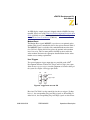
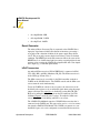
A block diagram of the eZ80® Development Platform and the eZ80F92
Flash Module is shown in Figure 1.
Peripheral Device Signals
eZ80F92
Peripheral Device Signals
Address Bus
Data Bus
Address Bus
eZ80™
Flash MPU
Module
Interface
Data Bus
RS232-0
(Console)
SRAM
(512 KB)
SRAM
(512 KB
up to 2 MB)
RS485
Battery &
Oscillator
for RTC
RS232-1
(Modem)
Embedded
Modem
IrDA
Transceiver
LED
(7x5 matrix)
Pushbuttons
GPIO
and
Address
Decoder
I2C
EEPROM
I2C
Register
Application Module Headers
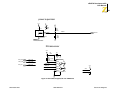
Figure 1. eZ80® Development Platform Block Diagram
with eZ80F92 Flash Module
eZ80® Development Platform Overview PRELIMINARY
UM013904-0203
eZ80F92 Development Kit
User Manual
5
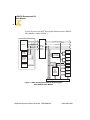
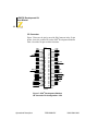
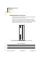
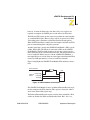
Figure 2 is a photographic representation of the eZ80® Development Platform segmented into its key blocks, as shown in the legend for the figure.
C
A
B
D
E
Note: Key to blocks A–E.
A. Power and serial communications.
B. eZ80F92 Flash Module interface.
C. Debug interface.
D. Application module interfaces.
E. GPIO and LED with Address Decoder.
Figure 2. The eZ80® Development Platform
UM013904-0203
PRELIMINARY eZ80® Development Platform Overview
eZ80F92 Development Kit
User Manual
6
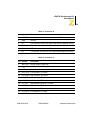
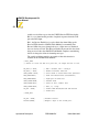
Figure 3 is a photographic representation of the eZ80F92 Flash Module
segmented into its key blocks, as shown in the legend for the figure.
Note: Key to blocks A–C.
A. eZ80F92 Flash Module interfaces.
B. CPU.
C. IrDA transceiver.
Figure 3. The eZ80F92 Flash Module
The structures of the eZ80® Development Platform and the eZ80F92
Flash Module are illustrated in the Schematic Diagrams starting on page
59.
eZ80® Development Platform Overview PRELIMINARY
UM013904-0203
eZ80F92 Development Kit
User Manual
7
eZ80® Development Platform
This section describes the eZ80® Development Platform hardware, its key
components and its interfaces, including detailed programmer interface
information such as memory maps, register definitions, and interrupt
usage.
Functional Description
The eZ80® Development Platform consists of seven major hardware
blocks. These blocks, listed below, are diagrammed in Figure 4.
•
•
eZ80F92 Flash Module interface (2 female headers)
•
•
•
•
•
Application Module interface (2 male headers)
UM013904-0203
Power supply for the eZ80® Development Platform, the eZ80F92
Flash Module, and application modules
GPIO and LED matrix
RS232 serial communications ports
Embedded modem interface
I2C devices
PRELIMINARY
eZ80® Development Platform
eZ80F92 Development Kit
User Manual
8
Peripheral Device Signals
eZ80™
Flash MPU
Module
Interface
Address Bus
Data Bus
RS232-0
(Console)
SRAM
(512 KB
up to 2 MB)
RS485
RS232-1
(Modem)
Embedded
Modem
LED
(7x5 matrix)
Pushbuttons
GPIO
and
Address
Decoder
I2C
EEPROM
I2C
Register
Application Module Headers
Figure 4. Basic eZ80® Development Platform Block Diagram
Functional Description
PRELIMINARY
UM013904-0203
eZ80F92 Development Kit
User Manual
9
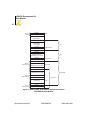
Physical Dimensions
The dimensions of the eZ80® Development Platform PCB is 177.8mm
x182.9mm. The overall height is 38.1mm. See Figure 5.
175.3 mm
43.2 mm
114.3 mm
96.5 mm
55.9 mm
157.5 mm
167.6 mm
5.1 mm
165.1 mm
5.1 mm
Figure 5. Physical Dimensions of the eZ80® Development Platform
UM013904-0203
PRELIMINARY
Functional Description
eZ80F92 Development Kit
User Manual
10
Operational Description
The eZ80® Development Platform can accept any eZ80®-core-based
modules, provided that the module interfaces correctly to the eZ80 ®
Development Platform. The purpose of the eZ80® Development Platform
is to provide the application developer with a tool to evaluate the features
of the eZ80F92 Flash MCU, and to develop an application without building additional hardware.
eZ80F92 Flash Module Interface
The eZ80F92 Flash Module interface provides easy connection of the
eZ80F92 Flash Module. It also provides easy connection for any eZ80 ®based module designed to this interface. This includes modules using
future eZ80® devices, and user-developed modules using current eZ80®
devices.
The eZ80F92 Flash Module interface consists of two 50-pin receptacles,
JP1 and JP2.
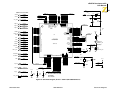
Peripheral Bus Connector
Figure 6 illustrates the pin layout of the Peripheral Bus Connector in the
50-pin header, located at position JP1 on the eZ80® Development Platform. Table 2 describes the pins and their functions.
Operational Description
PRELIMINARY
UM013904-0203
eZ80F92 Development Kit
User Manual
11
JP1
A6
A10
GND_EXT
A8
A13
A15
A18
A19
A2
A11
A4
A5
DIS_ETH
A21
A22
CS0
CS2
D1
D3
D5
D7
MREQ
GND_EXT
WR
BUSACK
1
3
5
7
9
11
13
15
17
19
21
23
25
27
29
31
33
35
37
39
41
43
45
47
49
2
4
6
8
10
12
14
16
18
20
22
24
26
28
30
32
34
36
38
40
42
44
46
48
50
A0
A3
V3.3_EXT
A7
A9
A14
A1 6
GND_EXT
A1
A12
A20
A17
DIS_FLASH
V3.3_EXT
A23
CS1
D0
D2
D4
GND_EXT
D6
IOREQ
RD
INSTRD
BUSREQ
HEADER 25X2
IDC50
Figure 6. eZ80® Development Platform
Peripheral Bus Connector Pin Configuration—JP1
UM013904-0203
PRELIMINARY
Operational Description
eZ80F92 Development Kit
User Manual
12
Table 2. eZ80® Development Platform
Peripheral Bus Connector Identification—JP1*
Signal Direction
Active Level
eZ80F92 Signal2
Pin #
Symbol
1
A6
Bidirectional
Yes
2
A0
Bidirectional
Yes
3
A10
Bidirectional
Yes
4
A3
Bidirectional
Yes
5
GND
6
VDD
7
A8
Bidirectional
Yes
8
A7
Bidirectional
Yes
9
A13
Bidirectional
Yes
10
A9
Bidirectional
Yes
11
A15
Bidirectional
Yes
12
A14
Bidirectional
Yes
13
A18
Bidirectional
Yes
14
A16
Bidirectional
Yes
15
A19
Bidirectional
Yes
Notes:
1. For the sake of simplicity in describing the interface, Power and Ground nets are omitted from
this table. The entire interface is represented in the eZ80F92 Module Schematics on pages 62
through 64.
2. The Power and Ground nets are connected directly to the eZ80F92 device.
3. External capacitive loads on RD, WR, IORQ, MREQ, D0–D7 and A0–A23 should be below 10pF
to satisfy the timing requirements for the eZ80® CPU. All unused inputs should be pulled to
either VDD or GND, depending on their inactive levels to reduce power consumption and to
reduce noise sensitivity. To prevent EMI, the EZ80CLK output can be deactivated via software in
the eZ80F91’s Peripheral Power-Down Register.
Operational Description
PRELIMINARY
UM013904-0203
eZ80F92 Development Kit
User Manual
13
Table 2. eZ80® Development Platform
Peripheral Bus Connector Identification—JP1* (Continued)
Signal Direction
Active Level
eZ80F92 Signal2
Pin #
Symbol
16
GND
17
A2
Bidirectional
Yes
18
A1
Bidirectional
Yes
19
A11
Bidirectional
Yes
20
A12
Bidirectional
Yes
21
A4
Bidirectional
Yes
22
A20
Bidirectional
Yes
23
A5
Bidirectional
Yes
24
A17
Bidirectional
Yes
25
DIS_ETH
Output
Low
No
26
DIS_FLASH
Output
Low
No
27
A21
28
VDD
29
30
Bidirectional
Yes
A22
Bidirectional
Yes
A23
Bidirectional
Yes
Notes:
1. For the sake of simplicity in describing the interface, Power and Ground nets are omitted from
this table. The entire interface is represented in the eZ80F92 Module Schematics on pages 62
through 64.
2. The Power and Ground nets are connected directly to the eZ80F92 device.
3. External capacitive loads on RD, WR, IORQ, MREQ, D0–D7 and A0–A23 should be below 10pF
to satisfy the timing requirements for the eZ80® CPU. All unused inputs should be pulled to
either VDD or GND, depending on their inactive levels to reduce power consumption and to
reduce noise sensitivity. To prevent EMI, the EZ80CLK output can be deactivated via software in
the eZ80F91’s Peripheral Power-Down Register.
UM013904-0203
PRELIMINARY
Operational Description
eZ80F92 Development Kit
User Manual
14
Table 2. eZ80® Development Platform
Peripheral Bus Connector Identification—JP1* (Continued)
Signal Direction
Active Level
eZ80F92 Signal2
CS0
Input
Low
Yes
32
CS1
Input
Low
Yes
33
CS2
Input
Low
Yes
34
D0
Bidirectional
Yes
35
D1
Bidirectional
Yes
36
D2
Bidirectional
No
37
D3
Bidirectional
Yes
38
D4
Bidirectional
Yes
39
D5
Bidirectional
Yes
40
GND
41
D7
Bidirectional
Yes
42
D6
Bidirectional
Yes
43
MREQ
Bidirectional
Low
Yes
44
IORQ
Bidirectional
Low
Yes
45
GND
Pin #
Symbol
31
Notes:
1. For the sake of simplicity in describing the interface, Power and Ground nets are omitted from
this table. The entire interface is represented in the eZ80F92 Module Schematics on pages 62
through 64.
2. The Power and Ground nets are connected directly to the eZ80F92 device.
3. External capacitive loads on RD, WR, IORQ, MREQ, D0–D7 and A0–A23 should be below 10pF
to satisfy the timing requirements for the eZ80® CPU. All unused inputs should be pulled to
either VDD or GND, depending on their inactive levels to reduce power consumption and to
reduce noise sensitivity. To prevent EMI, the EZ80CLK output can be deactivated via software in
the eZ80F91’s Peripheral Power-Down Register.
Operational Description
PRELIMINARY
UM013904-0203
eZ80F92 Development Kit
User Manual
15
Table 2. eZ80® Development Platform
Peripheral Bus Connector Identification—JP1* (Continued)
Signal Direction
Active Level
eZ80F92 Signal2
RD
Bidirectional
Low
Yes
47
WR
Bidirectional
Low
Yes
48
INSTRD
Input
Low
Yes
49
BUSACK
Input
Pull-Up 10KΩ; Low
Yes
50
BUSREQ
Output
Pull-Up 10KΩ; Low
Yes
Pin #
Symbol
46
Notes:
1. For the sake of simplicity in describing the interface, Power and Ground nets are omitted from
this table. The entire interface is represented in the eZ80F92 Module Schematics on pages 62
through 64.
2. The Power and Ground nets are connected directly to the eZ80F92 device.
3. External capacitive loads on RD, WR, IORQ, MREQ, D0–D7 and A0–A23 should be below 10pF
to satisfy the timing requirements for the eZ80® CPU. All unused inputs should be pulled to
either VDD or GND, depending on their inactive levels to reduce power consumption and to
reduce noise sensitivity. To prevent EMI, the EZ80CLK output can be deactivated via software in
the eZ80F91’s Peripheral Power-Down Register.
UM013904-0203
PRELIMINARY
Operational Description
eZ80F92 Development Kit
User Manual
16
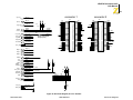
I/O Connector
Figure 7 illustrates the pin layout of the I/O Connector in the 50-pin
header, located at position JP2 on the eZ80® Development Platform.
Table 3 describes the pins and their functions.
JP2
PB7
PB5
PB3
PB1
GND_EXT
PC6
PC4
PC2
PC0
PD6
PD5
PD3
PD1
TDO
GND_EXT
TCK
RTC_VDD
IICSCL
IICSDA
FLASHWE
CS3
RESET
V3.3_EXT
HALT_SLP
V3.3_EXT
1
3
5
7
9
11
13
15
17
19
21
23
25
27
29
31
33
35
37
39
41
43
45
47
49
2
4
6
8
10
12
14
16
18
20
22
24
26
28
30
32
34
36
38
40
42
44
46
48
50
PB6
PB4
PB2
PB0
PC7
PC5
PC3
PC1
PD7
GND_EXT
PD4
PD2
PD0
TDI
TRIGOUT
TMS
EZ80CLK
GND_EXT
DIS_IRDA
WAIT
GND_EXT
NMI
HEADER 25X2
IDC50
Figure 7. eZ80® Development Platform
I/O Connector Pin Configuration—JP2
Operational Description
PRELIMINARY
UM013904-0203
eZ80F92 Development Kit
User Manual
17
Table 3. eZ80® Development Platform
I/O Connector Identification—JP2*
Signal Direction
Active Level
eZ80F92 Signal2
Pin #
Symbol
1
PB7
Bidirectional
Yes
2
PB6
Bidirectional
Yes
3
PB5
Bidirectional
Yes
4
PB4
Bidirectional
Yes
5
PB3
Bidirectional
Yes
6
PB2
Bidirectional
Yes
7
PB1
Bidirectional
Yes
8
PB0
Bidirectional
Yes
9
GND
10
PC7
Bidirectional
Yes
11
PC6
Bidirectional
Yes
12
PC5
Bidirectional
Yes
13
PC4
Bidirectional
Yes
14
PC3
Bidirectional
Yes
15
PC2
Bidirectional
Yes
16
PC1
Bidirectional
Yes
17
PC0
Bidirectional
Yes
18
PD7
Bidirectional
Yes
Notes:
1. For the sake of simplicity in describing the interface, Power and Ground nets are omitted from
this table. The entire interface is represented in the eZ80F92 Module Schematics on pages 62
through 64.
2. The Power and Ground nets are connected directly to the eZ80F92 device.
UM013904-0203
PRELIMINARY
Operational Description
eZ80F92 Development Kit
User Manual
18
Table 3. eZ80® Development Platform
I/O Connector Identification—JP2* (Continued)
Signal Direction
Active Level
eZ80F92 Signal2
Pin #
Symbol
19
PD6
20
GND
21
PD5
Bidirectional
Yes
22
PD4
Bidirectional
Yes
23
PD3
Bidirectional
Yes
24
PD2
Bidirectional
Yes
25
PD1
Bidirectional
Yes
26
PD0
Bidirectional
Yes
27
TDO
Input
Yes
28
TDI/ZDA
Output
Yes
29
GND
30
TRIGOUT
Input
31
TCK/ZCL
Output
32
TMS
Output
33
RTC_VDD
34
EZ80CLK
35
SCL
36
GND
Bidirectional
High
Yes
High
Yes
Input
Yes
Bidirectional
Yes
Notes:
1. For the sake of simplicity in describing the interface, Power and Ground nets are omitted from
this table. The entire interface is represented in the eZ80F92 Module Schematics on pages 62
through 64.
2. The Power and Ground nets are connected directly to the eZ80F92 device.
Operational Description
PRELIMINARY
UM013904-0203
eZ80F92 Development Kit
User Manual
19
Table 3. eZ80® Development Platform
I/O Connector Identification—JP2* (Continued)
Pin #
Symbol
37
SDA
38
GND
39
FlashWE
40
GND
41
CS3
42
DIS_IrDA
43
RESET
44
WAIT
45
VDD
46
GND
47
HALT_SLP
48
NMI
49
VDD
50
Reserved
Signal Direction
Active Level
Bidirectional
eZ80F92 Signal2
Yes
Output
Low
No
Input
Low
Yes
Output
Low
No
Bidirectional
Low
Yes
Output
Pull-Up 10KΩ; Low
Yes
Input
Low
Yes
Output
Low
Yes
Notes:
1. For the sake of simplicity in describing the interface, Power and Ground nets are omitted from
this table. The entire interface is represented in the eZ80F92 Module Schematics on pages 62
through 64.
2. The Power and Ground nets are connected directly to the eZ80F92 device.
Almost all of the connectors’ signals are received directly from the CPU.
Three input signals, in particular, offer options to the application developer by disabling certain functions of the eZ80F92 Flash Module.
UM013904-0203
PRELIMINARY
Operational Description
eZ80F92 Development Kit
User Manual
20
These three inputs are:
•
•
•
Disable Flash (DIS_Flash)*
Flash Write Enable (FlashWE)*
Disable IrDA (DIS_IrDA)
These three signals are described below.
Disable Flash*
When active Low, the DIS_Flash input signal disables the Flash chip on
the eZ80F92 Flash Module.
Flash Write Enable*
When active Low, the FlashWE input signal enables Write operations on
the Flash boot block of the eZ80F92 Flash Module.
Disable IrDA
When the DIS_IrDA input signal is pulled Low, the IrDA transceiver,
located on the eZ80F92 Flash Module, is disabled. As a result, UART0
can be used with the RS232 or the RS485 interfaces on the eZ80 ® Development Platform.
Note: *These inputs are only used if external Flash is present on the eZ80F92
Flash Module (as shipped from the factory, external Flash is not
installed).
Application Module Interface
An Application Module Interface is provided to allow the user to add an
application-specific module to the eZ80® Development Platform.
ZiLOG’s Thermostat Application Module (not provided in the kit) is an
example application-specific module that demonstrates an HVAC control
system. Implementing an application module with the Application Module Interface requires that the eZ80F92 Flash Module also be mounted on
Operational Description
PRELIMINARY
UM013904-0203
eZ80F92 Development Kit
User Manual
21
the eZ80® Development Platform, because the eZ80F92 Flash Module
features the eZ80F92 microcontroller. To mount an application module,
use the two male headers J6 and J8.
Jumper J6 carries the General Purpose Input/Output ports (GPIO), and
jumper J8 carries memory and control signals. To design an application
module, the user should be familiar with the architecture and features of
the eZ80F92 Flash Module currently installed. Tables 4 and 5 list the signals and functions related to each of these jumpers by pin. Power and
ground signals are omitted for the sake of simplicity.
Table 4. GPIO Connector J6*
Signal
Pin #
Function
Direction
SCL
5
I2C Clock
Bidirectional
SDA
7
I2C
Bidirectional
MOD_DIS
9
Modem Disable
MWAIT
13
Wait signal for the Input
CPU
EM_D0
15
Emulated Port A, Bidirectional
Bit 0
CS3
17
Chip Select 3 of
the CPU
EM_D[7:1]
21,23,25, Emulated Port A, Bidirectional
27,29,31, Bit [7:1]
33
Reserved
35
Data
Input
Output
Notes
If a shunt is installed between
pins 6 and 9, the modem
function on the eZ80®
Development Platform is
disabled.
This signal is also present on
the J8.
Note: *All of the signals are driven directly by the CPU.
UM013904-0203
PRELIMINARY
Operational Description
eZ80F92 Development Kit
User Manual
22
Table 4. GPIO Connector J6* (Continued)
Signal
Pin #
Function
Direction
PC[7:0]
39,41,43, Port C, Bit [7:0]
45,47,49,
51,53
ID_[2:0]
6,8,10
eZ80®
Development
Platform ID
Output
CON_DIS
12
Console Disable
Input
Reserved
16,18
PD[7:0]
22,24,26, Port D, Bit[7:0]
28,30,32,
34,36
Bidirectional
PB[7:0]
40,42,44, Port B, Bit[7:0]
46,48,50,
52,54
Bidirectional
Notes
Bidirectional
If a shunt is installed between
pins 12 and 14, the Console
function on the eZ80®
Development Platform is
disabled.
Note: *All of the signals are driven directly by the CPU.
Operational Description
PRELIMINARY
UM013904-0203
eZ80F92 Development Kit
User Manual
23
Table 5. CPU Bus Connector J8*
Signal
Pin #
Function
Direction
A[0:7]
3–10
Address Bus, Low Byte
Output
A[8:15]
13–20
Address Bus, High Byte
Output
A[16:23]
23–30
Address Bus, Upper Byte
Output
RD
33
Read Signal
Output
RESET
35
Push Button Reset
Output
BUSACK
37
CPU Bus Acknowledge Signal
Output
NMI
39
Nonmaskable Interrupt
Input
D[0:7]
43–50
Data Bus
Bidirectional
CS[0:3]
53–56
Chip Selects
MREQ
57
Memory Request
Output
WR
34
WRITE Signal
Output
INSTRD
36
Instruction Fetch
Output
BUSREQ
38
CPU Bus Request signal
PHI
40
Clock output of the CPU
Output
Note: *All of the signals except BUSACK and INSTRD are driven by low-voltage
CMOS technology (LVC) drivers.
I/O Functionality
The eZ80190 microprocessor features General-Purpose I/O functionality
at Port A. The eZ80F92 device does not incorporate this Port A feature.
The eZ80® Development Platform provides additional I/O functionality,
featuring GPIO for devices without Port A, an LED matrix, a modem
reset, and two user triggers.
UM013904-0203
PRELIMINARY
Operational Description
eZ80F92 Development Kit
User Manual
24
These functions are memory-mapped with an address decoder based on
the Generic Array Logic GAL22lV10D (U15) device manufactured by
Lattice Semiconductor, and a bidirectional latch (U16). Additionally, U15
is used to decode addresses for access to the 7x5 LED matrix.
Table 6 lists the memory map addresses to registers that allow access to
the above functions. The register at address 800000h controls GPIO Port
A Output Control and LED Anode register functions. The register at
address 800001h controls the register functions for the LED cathode,
modem reset, and user triggers. Address 800002h controls GPIO Port A
data.
Table 6. LED and Port Emulation Addresses
Address
Register Function
Access
800000h
LED Anode/GPIO Port output control
WR
800001h
LED Cathode/Modem/Trig
WR
800002h
GPIO Data
RD/WR
Port A Emulation
GPIO Port A is emulated with the use of the GPIO Output Control Register and the GPIO Data Register. If bit 7 in the GPIO Output Control Register is 1, all of the lines on GPIO Port A are configured as input ports. If
this bit is 0, all of the lines on Port A are configured as output ports.
Table 7 lists the multiple functions of the register.
Table 7. LED Anode/GPIO Port A Output Control Register
Bit #
Function
7
6
5
4
3
2
1
0
Anode Col 1
X
Anode Col 2
X
Anode Col 3
Operational Description
X
PRELIMINARY
UM013904-0203
eZ80F92 Development Kit
User Manual
25
Table 7. LED Anode/GPIO Port A Output Control Register (Continued)
Bit #
Function
7
6
5
4
3
Anode Col 4
2
1
0
X
Anode Col 5
X
Anode Col 6
X
Anode Col 6
X
GPIO Output
X
The GPIO Data Register receives inputs or provides outputs for each of
the seven GPIO Port A lines, depending on the configuration of the port.
See Table 8.
Table 8. GPIO Data Register
Function/Bit #
7
6
5
4
3
2
1
0
GPIO D0
X
GPIO D1
X
GPIO D2
X
GPIO D3
X
GPIO D4
X
GPIO D5
X
GPIO D6
GPIO D7
X
X
LED Matrix
The one 7x5 LED matrix device on the eZ80® Development Platform is a
memory-mapped device that can be used to display information, such as
programmed alphanumeric characters. For example, the LED display
UM013904-0203
PRELIMINARY
Operational Description
eZ80F92 Development Kit
User Manual
26
sample program that is shipped with this kit displays the alphanumeric
message:
eZ80
To illuminate any LED in the matrix, its respective anode bit must be set
to 1 and its corresponding cathode bit must be set to 0.
Bits 0–6 in Table 7 are LED anode bits. They must be set High (1) and
their corresponding cathode bits, bits 0–4 in Table 9, must be set Low (0)
to illuminate each of the LED’s, respectively.
Bit 7 in Table 7 does not carry any significance within the LED matrix. It
is used for GPIO as a Port A control bit.
Table 9 indicates the multiple register functions of the LED cathode,
modem, and triggers. This table shows the bit configuration for each cathode bit. Bits 5, 6, and 7 do not carry any significance within the LED
matrix. These three bits are control bits for the modem reset, Trig1, and
Trig2 functions, respectively.
Table 9. Bit Access to the LED Cathode, Modem, and Triggers
Bit #
Function
7
6
5
4
3
2
1
0
Cathode Row 5
X
Cathode Row 4
X
Cathode Row 3
X
Cathode Row 2
X
Cathode Row 1
X
Modem RST
X
Trig 1
Trig 2
Operational Description
X
X
PRELIMINARY
UM013904-0203
eZ80F92 Development Kit
User Manual
27
An LED display sample program is shipped with the eZ80F92 Development Kit. Please refer to the eZ80Acclaim! Development Kits Quick Start
Guide (QS0020) or to the Tutorial section in the ZiLOG Developer Studio—eZ80Acclaim! User Manual (UM0144).
Modem Reset
The Modem Reset signal, MRESET, is used to reset an optional socket
modem. This signal is controlled by bit 5 in the register shown in Table 9.
The MRESET signal is available at the embedded modem socket interface (J9, Pin1). Setting this bit Low places the optional socket modem
into a reset state. The user must pull this bit High again to enable the
socket modem. Reference the appropriate documentation for the socket
modem to reset timing requirements.
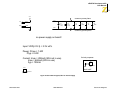
User Triggers
Two general-purpose trigger output pins are provided on the eZ80 ®
Development Platform. Labeled J21 (Trig2) and J22 (Trig1), these pins
allow the user a way to trigger external equipment to aid in the debug of
the system. See Figure 8 for trigger pin details.
J21
J22
Ground
Trigger output
Trig2
Trig1
Figure 8. Trigger Pins J21 and J22
Bits 6 and 7 in Table 9 are the control bits for the user triggers. If either
bit is a 1, the corresponding Trig1 and Trig2 signals are driven High. If
either bit is 0, the corresponding Trig1 and Trig2 signals are driven Low.
UM013904-0203
PRELIMINARY
Operational Description
eZ80F92 Development Kit
User Manual
28
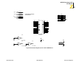
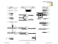
Embedded Modem Socket Interface
The eZ80® Development Platform features a socket for an optional 56K
modem (a modem is not included in the kit).
Connectors J1, J5, and J9 provide connection capability. The modem
socket interface provided by these three connectors is shown in Figure 9.
Tables 10 through 12 identify the pins for each connector. The embedded
modem utilizes UART1, which is available via the Port C pins.
J5
1
J1
2
2
4
24
25
26
27
J9
1
28
29
3
6
7
30
31
8
9
32
Figure 9. Embedded Modem Socket Interface—J1, J5, and J9
Table 10. Connector J5
Pin Symbol
Description
1
M-TIP
Telephone Line Interface—TIP.
2
M-RING
Telephone Line Interface—RING.
Operational Description
PRELIMINARY
UM013904-0203
eZ80F92 Development Kit
User Manual
29
Table 11. Connector J9
Pin Symbol
Description
1
MRESET
Reset, active Low, 50–100ms. Closure to GND for reset.
3
GND
Ground.
6
D1
DCD indicator; can drive an LED anode without additional circuitry.
7
D2
RxD indicator; can drive an LED anode without additional circuitry.
8
D3
DTR indicator; can drive an LED anode without additional circuitry.
9
D4
TxD indicator; can drive an LED anode without additional circuitry.
Table 12. Connector J1
Pin Symbol
Description
2
MOD_DIS
Modem disable, active Low.
4
VCC
+5 VDC or +3.3 VDC input.
24
GND
Ground.
25
PC4_DTR1 DTR interface; TTL levels.
26
PC6_DCD1 DCD interface; TTL levels.
27
PC3_CTS1 CTS interface; TTL levels.
28
PC5_DSR1 DSR interface; TTL levels.
29
PC7_RI1
30
PC0_TXD1 TxD interface; TTL levels.
31
PC1_RXD1 RxD interface; TTL levels.
32
PC2_RTS1 RTS interface; TTL levels.
UM013904-0203
Ring Indicator interface; TTL levels.
PRELIMINARY
Operational Description
eZ80F92 Development Kit
User Manual
30
Components P4, T1, C3, C4, and U11 provide the phone line interface to
the modem. On the eZ80® Development Platform, LEDs D1, D2, D3, and
D4 function as status indicators for this optional modem.
The phone line connection for the modem is for the United States only.
Connecting the modem outside of the U.S. requires modification.
The tested modem for this eZ80F92 Development Kit is a MultiTech Systems (formerly Conexant) socket modem, part number SC56H1. Either
the 3.3V or the 5.0V version of the modem can be used. However, jumper
J12 should be configured accordingly—see Table 17. Information about
this modem and its interface is available in the SocketModem data sheet
from www.multitech.com.
eZ80® Development Platform Memory
Memory space on the eZ80® Development Platform consists of onboard
SRAM and additional SRAM footprints.
Onboard SRAM
The eZ80® Development Platform features 512KB SRAM at U20. This
SRAM provides the basic memory requirement for small applications
development. This SRAM is in the address range B80000h–BFFFFFh.
With the 512KB of SRAM on the eZ80F92 Flash Module, this addressing
structure provides 1MB of contiguous SRAM for immediate use. Chip
Select 2 is used to access the 512KB of SRAM on the eZ80® Development Platform.
Additional SRAM
The amount of eZ80® Development Platform memory can be extended if
required by adding SRAM devices. U19, U18, and U17 provide this capability. However, the user should be aware that additional SRAM must be
installed in the following order:
1. U19, address range B00000h–B7FFFFh
Operational Description
PRELIMINARY
UM013904-0203
eZ80F92 Development Kit
User Manual
31
2. U18, address range A80000h–AFFFFFh
3. U17, address range A00000h–A7FFFFh
If SRAM memory is installed in a different order than the above
sequence, SRAM will not be contiguous unless the user is able to change
the address decoder, U10. Memory access decoding is performed by this
address decoder, implemented in the Generic Array Logic device,
GAL22LV10D (U10).
On-Chip SRAM
The eZ80F92 device on the eZ80F92 Flash Module contains 8KB of onchip SRAM. Upon power-up, this SRAM is enabled and mapped to the
top 8KB of memory address space. Using the RAM Address Register,
this 8KB memory can be mapped to the top of any 64KB block. It can
also be disabled. Please see the eZ80F92/eZ80F92 Product Specification
(PS0153) for more information.
Flash Memory
The eZ80F92 Development Kit allows off-chip Flash memories between
1MB and 4MB. This Flash memory is entirely located on the eZ80F92
Flash Module (in footprint only; as shipped from the factory, external
Flash is not installed).
Memory Map
A memory map of the eZ80® CPU is illustrated in Figure 10. Flash memory and SRAM on the eZ80F92 Flash Module are addressed when CS0
and CS1 are active Low. SRAM on the eZ80® Development Platform is
addressed when CS2 is active Low.
The location of on-chip SRAM is programmable by setting the RAM
address upper byte register. The upper 8KB of any 64KB memory page
can be selected. Addresses to enabled on-chip memories assume priority
over all chip selects. Please refer to the eZ80F92/eZ80F92 Product Specification (PS0153) for more details.
UM013904-0203
PRELIMINARY
Operational Description
eZ80F92 Development Kit
User Manual
32
On-chip
SRAM
FFFFFFh
8 KB
FFE000h
Available
Address Space
DFFFFFh
SRAM Memory
up to 2 MB
CS1
C7FFFFh
Module SRAM
C00000h
BFFFFFh
Platform SRAM (512 KB)
B80000h
Platform Expansion
SRAM Memory up to 4 MB
80FFFFh
CS2
LED & GPIO
800000h
7FFFFFh
Off-chip
Flash memory
Expansion Module:
Flash Memory up to 4 MB
Up to 4 MB
400000h
3FFFFFh
Module Expansion
Flash Memory up to 4 MB
Off-chip
Flash memory
CS0 (8 MB)
120000h
11FFFFh
Flash Memory
Up to 4 MB
1 MB
020000h
On-chip
Flash memory
01FFFFh
000000h
128 KB
Figure 10. Memory Map of the eZ80® Development Platform
and eZ80F92 Flash Module
Operational Description
PRELIMINARY
UM013904-0203
eZ80F92 Development Kit
User Manual
33
LEDs
As stated earlier, LEDs D1, D2, D3, and D4 function as status indicators
for an optional modem. This section describes each LED and the LED
matrix device.
Data Carrier Detect
The Data Carrier Detect (DCD) signal at D1 indicates that a good carrier
signal is being received from the remote modem.
RX
The RX signal at D2 indicates that data is received from the modem.
Data Terminal Ready
The Data Terminal Ready (DTR) signal at D3 informs the modem that the
PC is ready.
TX
The TX signal at D4 indicates that data is transmitted to the modem.
Push Buttons
The eZ80® Development Platform provides user controls in the form of
push buttons. These push buttons serve as input devices to the eZ80F92
microcontroller. The programmer can use them as necessary for application development. All push buttons are connected to the GPIO Port B
pins.
PB0
The PB0 push button switch, SW1, is connected to bit 0 of GPIO Port B.
This switch can be used as the port input if required by the user.
UM013904-0203
PRELIMINARY
Operational Description
eZ80F92 Development Kit
User Manual
34
PB1
The PB1 push button switch, SW2, is connected to bit 1 of GPIO Port B.
This switch can be used as the port input if required by the user.
PB2
The PB2 push button switch, SW3, is connected to bit 2 of GPIO Port B.
This switch can be used as the port input if required by the user.
RESET
The Reset push button switch, SW4, resets the eZ80® CPU and the eZ80®
Development Platform.
Jumpers
The eZ80® Development Platform provides a number of jumpers that are
used to enable or disable functionality on the platform, enable or disable
optional features, or to provide protection from inadvertent use.
Jumper J2
The J2 jumper connection enables/disables IrDA transceiver functionality. When the shunt is placed, IrDA communication is disabled. See
Table 13.
Table 13. J2—DIS_IrDA
Shunt
Status
Function
Affected Device
In
IrDA interface disabled UART0 is configured to work with the RS232 or the
RS485 interfaces.
Out
IrDA interface enabled The IrDA and UART0 interfaces on the eZ80F92 Flash
Module perform their functions.
Operational Description
PRELIMINARY
UM013904-0203
eZ80F92 Development Kit
User Manual
35
Jumper J3
The J3 jumper connection controls Port A emulation mode and communication with the 7x5 LED. When the shunt is placed, Port A emulation is
disabled. See Table 14.
Table 14. J3—DIS_EM
Shunt
Status
Function
Affected Device
In
Application Module
Hardware Disabled
Communication with 7x5 LED and Port emulation
circuit is disabled.
Out
Application Module
Hardware Enabled
Communication with 7x5 LED and Port A emulation
circuit is enabled.
Jumper J7
The J7 jumper connection controls Flash boot loader programming. When
the shunt is placed, overwriting of the Flash boot loader program is
enabled. See Table 15.
Table 15. J7—FlashWE (Off-Chip)*
Shunt
Status
Function
Affected Device
Out
The Flash boot sector of the eZ80F92 Flash boot sector of the eZ80F92 Flash
Flash Module is write-protected.
Module.
In
The Flash boot sector of the eZ80F92 Flash boot sector of the eZ80F92 Flash
Flash Module is enabled for writing or Module.
overwriting.
Note: As shipped from the factory, external Flash memory is not installed.
UM013904-0203
PRELIMINARY
Operational Description
eZ80F92 Development Kit
User Manual
36
Jumper J11
The J11 jumper connection controls access to the Flash memory device.
When the shunt is placed, access to the Flash device is disabled/prevented. See Table 16.
Table 16. J11—DIS_Flash (Off-Chip)*
Shunt
Status
Function
Affected Device
In
All access to Flash on the eZ80F92
Flash Module is disabled.
Flash on eZ80F92 Flash Module.
Out
Flash on the eZ80F92 Flash Module
is enabled.
Flash on eZ80F92 Flash Module.
Note: As shipped from the factory, external Flash memory is not installed.
Jumper J12
The J12 jumper connection controls the selection of a 5V or 3VDC
power supply to the embedded modem, if an embedded modem is used.
See Table 17.
Table 17. J12—5VDC/3.3VDC for an Embedded Modem
Shunt
Status
Function
Affected Device
1–2
5VDC is provided to power the embedded modem.
Embedded modem.
2–3
3.3VDC is provided to power the embedded modem. Embedded modem.
Operational Description
PRELIMINARY
UM013904-0203
eZ80F92 Development Kit
User Manual
37
Jumper J14
The J14 jumper connection controls the polarity of the Ring Indicator.
See Table 18.
Table 18. J14—RI
Shunt
Status
Function
Affected Device
1–2
The Ring Indicator for UART1 is inverted.
UART1.
2–3
The Ring Indicator for UART1 is not inverted.
UART1.
Jumper J15
The J15 jumper connection controls the selection RS485 circuit along
with UART0. When the shunt is placed, the RS485 circuit is enabled. See
Table 19. RS485 functionality will be available in future eZ80 ® devices.
Table 19. J15—RS485_1_EN*
Shunt
Status
Function
Affected Device
In
The RS485 circuit is enabled on UART0.
The UART0 CONSOLE interface and IrDA are
disabled.
IrDA, UART0 CONSOLE
interface, RS485 interface.
Out
The RS485 circuit is disabled on UART0.
IrDA, UART0 CONSOLE
interface, RS485 interface.
Note: *To enable the RS485 circuit, the corresponding IrDA/RS232 circuit must be disabled.
UM013904-0203
PRELIMINARY
Operational Description
eZ80F92 Development Kit
User Manual
38
Jumper J16
The J16 jumper connection controls the selection of the RS485 circuit.
However, UART1 MODEM interface and the socket modem interface are
disabled if the RS485 circuit is enabled. When the shunt is placed, the
RS485 circuit is enabled. See Table 20.
Table 20. J16—RS485_2_EN
Shunt
Status
Function
Affected Device
In
The RS485 circuit is enabled on UART1.
The UART1 MODEM interface and the
Socket Modem interface are disabled.
UART1 MODEM interface,
Socket Modem Interface, and
RS485 interface.
Out
The RS485 circuit is disabled on UART1.
UART1 MODEM interface,
Socket Modem Interface, and
RS485 interface.
Jumper J17
The J17 jumper connection controls the selection of the RS485 termination resistor circuit. When the shunt is placed, the RS485 termination
resistor circuit is enabled. See Table 21.
Table 21. J17—RT_1*
Shunt
Status
Function
Affected Device
In
The Termination Resistor for RS485_1 is IN.
RS485 interface.
Out
The Termination Resistor for RS485_1 is OUT.
RS485 interface.
Note: *Before enabling the termination resistor, ensure that the device is located at the end of the
interface line.
Operational Description
PRELIMINARY
UM013904-0203
eZ80F92 Development Kit
User Manual
39
Jumper J18
The J18 jumper connection controls the selection of the RS485 termination resistor circuit. When the shunt is placed, the RS485 termination
resistor circuit is enabled. See Table 22.
Table 22. J18—RT_2*
Shunt
Status
Function
Affected Device
In
The Termination Resistor for RS485_2 is IN.
RS485 interface.
Out
The Termination Resistor for RS485_2 is OUT.
RS485 interface.
Note: *Before enabling the termination resistor, ensure that the device is located at the end of the
interface line.
Connectors
A number of connectors are available for connecting external devices
such as the ZPAKII emulator, PC serial ports, external modems, the console, and LAN/telephone lines.
J6 and J8 are the headers, or connectors, that provide pin-outs to connect
any external application module, such as ZiLOG’s Thermostat Application Module.
Connector J6
The J6 connector provides pin-outs to make use of GPIO functionality.
Connector J8
The J8 connector provides pin-outs to access memory and other control
signals.
UM013904-0203
PRELIMINARY
Operational Description
eZ80F92 Development Kit
User Manual
40
Console
Connector P2 is the RS232 terminal, which can be used for observing the
console output. P2 can be connected to the HyperTerminal if required.
Modem
Connector P3 provides a terminal for connecting an external modem, if
used with the eZ80F92 Development Kit. RS485 functionality will be
available in future eZ80® devices.
I2C Devices
The two I2C devices on the eZ80® Development Platform are the U2
EEPROM and the U13 Configuration register. The EEPROM provides
16KB of memory. The Configuration register provides access to control
the configuration of an application-specific function at the Application
Module Interface. Neither device is utilized by the eZ80F92 Development
Kit software. The user is free to develop proprietary software for these
two devices. The addresses for accessing these devices are listed in
Table 23.
Table 23. I2C Addresses
Device/Bit #
7
6
5
4
3
2
1
0
EEPROM (U10)*
1
0
1
0
0
A1
A0
R/W
Configuration Register (U13)
1
0
0
1
1
1
0
R/W
Note: *EEPROM address bits A0 and A1 are configured for 0s.
I2C Devices
PRELIMINARY
UM013904-0203
eZ80F92 Development Kit
User Manual
41
DC Characteristics
Understanding proper DC current requirements for the eZ80® Development Platform when application modules are plugged into it is very
important for developing applications. This section provides an estimate
of the average current requirement when different combinations of these
application modules are plugged in to the eZ80® Development Platform.
The receiver supply current is 90–150µA and the transmitter supply current is 260mA when the LED is active. The measurements of current that
are shown in Table 24 are for the user’s reference. These values can vary
depending on the type of application that is developed to run with the
platform.
Table 24. DC Current Characteristics of the
eZ80® Development Platform with Different Module Loads
Platform/Modules Configurations
Current
Requirement (mA) Status
eZ80® Development Platform
and eZ80F92 Flash Module
173
When connected only to a
power supply, and when
no program is running.
eZ80® Development Platform,
eZ80F92 Flash Module, and Modem
Module
174
When connected only to a
power supply, and when
no program is running.
eZ80® Development Platform,
eZ80F92 Flash Module, and
Thermostat Application Module
195
When connected only to a
power supply, and when
no program is running.
eZ80® Development Platform,
eZ80F92 Flash Module, Modem
Module, and Thermostat Application
Module
203
When connected only to a
power supply, and when
no program is running.
eZ80® Development Platform
and eZ80F92 Flash Module
325
When the LED demo is
running.
UM013904-0203
PRELIMINARY
DC Characteristics
eZ80F92 Development Kit
User Manual
42
Table 24. DC Current Characteristics of the
eZ80® Development Platform with Different Module Loads (Continued)
Platform/Modules Configurations
Current
Requirement (mA) Status
eZ80® Development Platform,
eZ80F92 Flash Module, and Modem
Module
325
When the LED demo is
running.
eZ80® Development Platform,
eZ80F92 Flash Module, and
Thermostat Application Module
350
When the LED demo is
running.
eZ80® Development Platform,
eZ80F92 Flash Module, Modem
Module, and Thermostat Application
Module
360
When the LED demo is
running.
DC Characteristics
PRELIMINARY
UM013904-0203
eZ80F92 Development Kit
User Manual
43
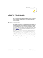
eZ80F92 Flash Module
This section describes the eZ80F92 Flash Module hardware, its interfaces
and key components, including the CPU, real-time clock, IrDA transceiver, and memory.
Functional Description
The eZ80F92 Flash Module is a compact, high-performance module specially designed for the rapid development and deployment of embedded
systems. Additional devices such as serial ports, LED matrices, GPIO
ports, and I2C devices are supported when connected to the eZ80® Development Platform. A block diagram representing both of these boards is
shown in Figure 1 on page 4.
The eZ80F92 Flash Module is developed to be a plug-in module to the
eZ80® Development Platform. This small-footprint module provides a
CPU, RAM, an IrDA transceiver, and a real-time clock. This low-cost,
expandable module is powered by the eZ80F92 microcontroller, members
of ZILOG’s new eZ80® product family. The module also contains a battery and an oscillator in support of the on-chip Real-Time Clock (RTC).
The eZ80F92 Flash Module can also be used as a stand-alone development tool when provided with an external power source.
UM013904-0203
PRELIMINARY
eZ80F92 Flash Module
eZ80F92 Development Kit
User Manual
44
Physical Dimensions
The dimensions of the eZ80F92 Flash Module PCB is 64x64mm. With
an RJ-45 Ethernet connector, the overall height is 25mm. See Figure 11.
63.5 mm
8.5 mm
8.3 mm
max.
1
1
I/O Connector
Bus Connector
2.54 mm
Top View
64 mm
9 mm
2.7 mm
6.2 mm
IrDA
7 mm
55.88 mm
Figure 11. Physical Dimensions of the eZ80F92 Flash Module
Functional Description
PRELIMINARY
UM013904-0203
eZ80F92 Development Kit
User Manual
45
Figure 12 illustrates the top layer silkscreen of the eZ80F92 Flash Module.
Figure 12. eZ80F92 Flash Module—Top Layer
UM013904-0203
PRELIMINARY
Functional Description
eZ80F92 Development Kit
User Manual
46
Figure 13 illustrates the bottom layer silkscreen of the eZ80F92 Flash
Module.
Figure 13. eZ80F92 Flash Module—Bottom Layer
Functional Description
PRELIMINARY
UM013904-0203
eZ80F92 Development Kit
User Manual
47
Operational Description
The purpose of the eZ80F92 Flash Module as a feature of the eZ80F92
Development Kit is to provide the application developer with a plug-in
tool to evaluate the memory, IrDA, and other features of the eZ80F92
device.
eZ80F92 Flash Module Memory
The eZ80F92 Flash Module comprises both off-chip SRAM and on-chip
Flash memory, which are described below.
Static RAM
The eZ80F92 Flash Module features 512KB of fast SRAM. Access speed
is typically 50ns, allowing zero-wait-state operation at 20MHz. With the
CPU at 20MHz, SRAM can be accessed with zero wait states in eZ80
mode. CS1_CTL (chip select CS1) can be set to 08h (no wait states).
Flash Memory
The eZ80F92 Flash Module features 128KB of Flash memory. This onchip memory can be programmed a single byte at a time, or in bursts of
up to 128 bytes. Write operations can be performed using either memory
or I/O instructions. Erasing bytes in Flash memory returns them to a value
of FFh. Both the MASS ERASE and PAGE ERASE operations are selftimed by the Flash controller, leaving the CPU free to execute other operations in parallel. Upon power-up, the on-chip Flash memory is located in
the address range 000000h–01FFFFh. Four wait states are programmed
in Flash control register F8h.
On-chip Flash memory is prioritized over all external Chip Selects, can be
enabled or disabled (power-on enabled), and can be programmed within
any 128KB address space in the 16MB address range.
The eZ80F92 Flash Module features the following memory configurations:
UM013904-0203
PRELIMINARY
Operational Description
eZ80F92 Development Kit
User Manual
48
•
•
•
On-chip SRAM: 8KB
Off-chip SRAM: 512KB
On-chip Flash: 128KB
Reset Generator
The onboard Reset Generator Chip is connected to the eZ80F92 Reset
input pin. It performs reliable Power-On Reset functions, generating a
reset pulse with a duration of 200ms if the power supply drops below
2.93V. This reset pulse ensures that the board always starts in a defined
condition. The RESET pin on the I/O connector reflects the status of the
RESET line. It is a bidirectional pin for resetting external peripheral components or for resetting the eZ80F92 Development Kit with a low-impedance output (e.g. a 100-Ohm push button).
IrDA Transceiver
An onboard IrDA transceiver (ZiLOG ZHX1810) is connected to PD0
(TX), PD1 (RX), and PD2 (Shutdown, IR_SD). The IrDA transceiver is
of the LED type 870nm Class 1.
The IrDA transceiver is accessible via the IrDA controller attached to
UART0 on the eZ80F92 device. The UART0 console and the IrDA transceiver cannot be used simultaneously.
To use the UART0 for console or to save power, the transceiver can be
disabled by the software or by an off-board signal when using the proper
jumper selection. The transceiver is disabled by setting PD2 (IR_SD)
High or by pulling the DIS_IRDA pin on the I/O connector Low. The
shutdown feature is used for power savings. To enable the IrDA transceiver, DIS_IRDA is left floating and PD2 is set to Low.
The eZ80F92 Flash Module contains a ZiLOG IrDA transceiver that is
connected to the UART0 port. This port can be used as a wireless connection into the eZ80F92 Flash Module. The UART0 can connect to a standard RS232 port, or it can be configured to control the IrDA transceiver;
Operational Description
PRELIMINARY
UM013904-0203
eZ80F92 Development Kit
User Manual
49
however, it cannot do both at the same time. Only a few registers are
required to configure the UART0 port to send and receive IrDA data.
The RxD and TxD signals on the transceiver perform the same functions
as a standard RS232 port. However, these signals are processed as IrDA
3/16 coding pulses (sometimes called IrDA encoder/decoder pulses).
When the IrDA function is enabled, the final output to the RxD and TxD
pins are routed through the 3/16 pulse generator.
Another signal that is used in the eZ80F92 Flash Module’s IrDA system
is Shut_Down (SD). The SD pin is connected to PD2 on the eZ80F92
Flash Module. The IrDA control software on the user’s wireless device
must enable this pin to wake the IrDA transceiver. The SD pin must be set
Low to enable the IrDA transceiver. On the eZ80F92 Flash Module, a
two-input OR gate is used to allow an external pin to shut down the IrDA
transceiver. Both pins must be set Low to enable this function.
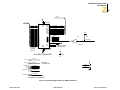
Figure 14 highlights the eZ80F92 Flash Module IrDA hardware connections.
External Disable
IrDA
eZ80L92
Device
PD2(IR_SD)
SD
PD1(RxD)
RD
PD0(TxD)
TD
Figure 14. IrDA Hardware Connections
The eZ80F92 Flash Module features an Infrared Encoder/Decoder register that configures the IrDA function. This register is located at address
0BFh in the internal I/O register map.
The Infrared Encoder/Decoder register contains three control bits. Bit 0
enables or disables the IrDA encoder/decoder block. Bit 1, if it is set,
UM013904-0203
PRELIMINARY
Operational Description
eZ80F92 Development Kit
User Manual
50
enables received data to pass into the UART0 Receive FIFO data buffer.
Bit 2 is a test function that provides a loopback sequence from the TxD
pin to the RxD input.
Bit 1, the Receive Enable bit, is used to block data from filling up the
Receive FIFO when the eZ80F92 Flash Module is transmitting data.
Because IrDA data passes through the air as a light source, transmitted
data can also be received. This Receive Enable bit prevents this data from
being received. After the eZ80F92 Flash Module completes transmitting,
this bit is changed to allow for incoming messages.
The code that follows provides an example of how this function is
enabled on the eZ80F92 Flash Module.
//Init_IRDA
// Ensure to first set PD2 as a port bit, an output and set it Low.
PD_ALT1 &= 0xFC;
// PD0 = uart0tx, PD1 = uart0_rx
PD_ALT2 |= 0x03;
// Enable alternate function
UART_LCTL0= 0x80;
// Select dlab to access baud rate generator
BRG_DLRL0=0x2F;
// Baud rate Masterclock/(16*baudrate)
BRG_DLRH0=0x00;
// High byte of baud rate
UART_LCTL0=0x00;
// Disable dlab
UART_FCTL0=0xC7;
// Clear tx fifo, enable fifo
UART_LCTL0=0x03;
// 8bit, N, 1 stop
IR_CTL = 0x03;
// enable IRDA Encode/decode and Receive
// enable bit.
//IRDA_Xmit
IR_CTL = 0x01;
//Disable receive
Putchar(0xb0);
//Output a byte to the uart0 port.
Operational Description
PRELIMINARY
UM013904-0203
eZ80F92 Development Kit
User Manual
51
DC Characteristics
As different combinations of application modules are loaded onto the
eZ80® Development Platform, current requirements change. Please see
Table 24 on page 41 to reference current consumption values for these
different module combinations.
A 0.1-Farad capacitor is provided on the eZ80F92 Flash Module as a
short-term battery backup for the RTC (see the Schematic Diagrams on
page 59). The part number of the capacitor made by Panasonic is
EECS0HDV. The capacitor is connected to RTC_VDD to provide power
to the RTC when main power to the chip is removed; it is also connected
to the 3.3V supply to the chip for recharging. The RTC can operate down
to 3.0V; it requires 10µA of current. The (keep alive) time this capacitor
can supply power to the RTC, from 3.3V to 3.0V, is approximately 3000
seconds, or 50 minutes.
Flash Loader Utility
The Flash Loader utility allows the user a convenient way to program onchip Flash memory. Please refer to the External Flash Loader Product
User Guide (PUG0016) for more details.
Mounting the Module
When mounting the eZ80F92 Flash Module onto the eZ80® Development
Platform, check its orientation to the platform to ensure a correct fit. Pin 1
of JP1 on the eZ80® Development Platform must align with pin 1 of JP1
on the eZ80® Development Platform; Pin 1 of JP2 on the eZ80F92 Flash
Module must align with pin 1 of JP2 on the eZ80® Development Platform, etc.
UM013904-0203
PRELIMINARY
DC Characteristics
eZ80F92 Development Kit
User Manual
52
Changing the Power Supply Plug
The universal 9VDC power supply offers three different plug configurations and a tool that aids in removing one plug configuration to insert
another, as shown in Figure 15.
Figure 15. 9VDC Universal Power Supply Components
To exchange one plug configuration for another, perform the following
steps:
1. Place the tip of the removal tool into the round hole at the top of the
current plug configuration.
2. Press down to disengage the keeper tab and push the plug configuration out of its slot.
3. Select the plug configuration appropriate for your location, and insert
it into the slot formerly occupied by the previous plug configuration.
4. Push the new plug configuration down until it snaps into place, as
indicated in Figure 16.
Changing the Power Supply Plug
PRELIMINARY
UM013904-0203
eZ80F92 Development Kit
User Manual
53
Figure 16. Inserting a New Plug Configuration
UM013904-0203
PRELIMINARY
Changing the Power Supply Plug
eZ80F92 Development Kit
User Manual
54
ZPAKII
ZPAKII is a debug tool used to develop and debug hardware and software. It is a networked device featuring an Ethernet interface and an
RS232 console port. ZPAKII is shipped with a preconfigured IP address
that can be changed to suit the user on a local network. For more information about using and configuring ZPAKII, please refer to the
eZ80Acclaim! Development Kits Quick Start Guide (QS0020) and the
ZPAKII Product User Guide (PUG0015).
ZDI Target Interface Module
The ZDI Target Interface Module provides a physical interface between
ZPAKII and the eZ80® Development Platform. The TIM module supports
ZDI functions. For more information on using the TIM module or ZDI
please refer to the eZ80Acclaim! Development Kits Quick Start Guide
(QS0019), the eZ80F92 Ethernet Module Product Specification
(PS0186), and the eZ80F92 Flash Module Product Specification
(PS0189).
JTAG
Connector P1 is the JTAG connector on the eZ80® Development Platform. JTAG will be supported in the next offering of eZ80® products.
Application Modules
ZiLOG offers the Thermostat Application module, which can be used for
evaluating and developing process control and simple I/O applications.
The Thermostat Application module is equipped with an LCD display
that can be used to display process control and other physical parameters.
ZPAKII
PRELIMINARY
UM013904-0203
eZ80F92 Development Kit
User Manual
55
For additional reading about the Thermostat application, please see the
Java Thermostat Demo Application Note (AN0104) on zilog.com.
UM013904-0203
PRELIMINARY
Application Modules
eZ80F92 Development Kit
User Manual
56
ZDS II
ZiLOG Developer Studio II (ZDS II) Integrated Development Environment is a complete stand-alone system that provides a state-of-the-art
development environment. Based on the Windows® Win98SE/NT4.0SP6/Win2000-SP2/WinXP user interfaces, ZDS II integrates a languagesensitive editor, project manager, C-Compiler, assembler, linker, librarian,
and source-level symbolic debugger that supports the eZ80F92.
For further details about ZDS II for eZ80Acclaim! products, please refer
to the ZiLOG Developer Studio—eZ80Acclaim! User Manual
(UM0144).
ZDS II
PRELIMINARY
UM013904-0203
eZ80F92 Development Kit
User Manual
57
Troubleshooting
Overview
Before contacting ZiLOG Customer Support to submit a problem report,
please follow these simple steps. If a hardware failure is suspected, contact a local ZiLOG representative for assistance.
Cannot Download Code
If you are unable to download code to RAM using ZDS, make sure to
press and release the Reset button on the eZ80® Development Platform
prior to selecting Build → Debug → Reset + Go in ZDS.
No Output on Console Port
The eZ80F92 Development Kit is shipped with a Flash Loader utility that
is loaded in the protected boot sector of Flash memory (U3). Upon powerup of the eZ80® Development Platform and the eZ80F92 Flash MCU
Module, the eZ80F92 device on the module starts running code from this
Flash memory area. This code enables the Console port with settings of
57.6kbps, 8, N, 1.
The Console checks the Receive buffer. If a space character is received on
the Console port, the Flash Loader utility is enabled and a boot message
should be displayed on your connected device. If no message is displayed, check the following:
•
•
UM013904-0203
Jumper J2 must be ON (IrDA is disabled)
On Connector J6, the jumper must be removed from pins 6 and 9 (pin
names con_dis and GND).
PRELIMINARY
Troubleshooting
eZ80F92 Development Kit
User Manual
58
IrDA Port Not Working
If you plan on using the IrDA transceiver on the eZ80F92 Flash Module,
make sure the hardware is set up as follows:
•
Jumper J2 must be OFF (to enable the control gate that drives the
IrDA device)
•
Set port pin PD2 Low. When this port pin and Jumper J2 are turned
OFF, the IrDA device is enabled.
•
Install a jumper on connector J6 across pin names con_dis and GND
to disable the console serial port driver
Contacting ZiLOG Customer Support
For additional troubleshooting solutions, see ZDS Online Help.
For valuable information about hardware and software development tools,
visit ZiLOG Customer Support online. Download the latest released version of ZiLOG Developer Studio!
Get the latest software updates from ZiLOG as soon as they are available!
UM013904-0203
eZ80F92 Development Kit
User Manual
Schematic Diagrams
59
eZ80® Development Platform
Figures 17 through 21 diagram the layout of the eZ80® Development Platform.
MA6
MA10
DO NOT USE J6_17 AND J6_35
VCC
1
3
5
7
9
11
13
15
17
19
21
23
25
27
29
31
33
35
37
39
41
43
45
47
49
51
53
55
57
59
9V_DC
9VDC
SCL
SDA
GND
-MOD_DIS
-MWAIT
EM_D0
-CS3
GND
EM_D7
EM_D6
EM_D5
EM_D4
EM_D3
EM_D2
EM_D1
GND
PC7_RI1
PC6_DCD1
PC5_DSR1
PC4_DTR1
PC3_CTS1
PC2_RTS1
PC1_RXD1
PC0_TXD1
GND
GND
A8
A10
A12
A14
GND
A16
A18
A20
A22
VDD
-RESET
GND
D0
D2
D4
D6
GND
-CS0
-CS2
-MEMRQ VDD
ID_2
ID_1
ID_0
-CON_DIS
GND
-DIS_ETH
GND
PD7_RI0
PD6_DCD0
PD5_DSR0
PD4_DTR0
PD3_CTS0
PD2_RTS0
PD1_RXD0
PD0_TXD0
GND
PB7_MOSI
PB6_MISO
PB5_T5_O
PB4_T4_O
PB3_SCK
PB2_SS
PB1_T1_I PB2_SS
PB0_T0_I PB1_T1_I
PB0_T0_I
A1
A3
A5
A7
GND
A9
A11
A13
A15
VDD
R3
10K
GND
A17
A19
A21
A23
VDD
PHI
GND
D1
D3
D5
D7
-CS1
-CS_EX
-IORQ
J4
VDD
1
3
5
GND
MA23
-M_CS1
MD0
MD2
MD4
MD6
-M_IORQ
-M_RD
INSTRD
-BUSREQ
2
4
6
8
11
13
15
17
R2
10K
PB6_MISO
PB4_T4_O
PB2_SS
PB0_T0_I
PC7_RI1
PC5_DSR1
PC3_CTS1
PC1_RXD1
PD7_RI0
GND
PD4_DTR0
PD2_RTS0
PD0_TXD0
TDI
TRIGOUT
TMS
M_PHI
GND
A1
A2
A3
A4
A5
A6
A7
A8
1
19
VDD
Y1
Y2
Y3
Y4
Y5
Y6
Y7
Y8
1OE
2OE
VCC
GND
2
4
6
8
11
13
15
17
GND
1
19
A1
A2
A3
A4
A5
A6
A7
A8
Y1
Y2
Y3
Y4
Y5
Y6
Y7
Y8
1OE
2OE
VCC
GND
M_TIP
M_RING
J9
DCD
1
2
1
TVCC_RESETn
VDD
1
3
5
7
9
11
13
2
4
6
8
10
12
14
0
2
D3
1
SDA
8
VDD
4
3
GND
WP NC
GND
C30
0.1uF
HEADER 2
A8
A9
A10
A11
A12
A13
A14
A15
18
16
14
12
9
7
5
3
20
10
-FLASHWE
GND
1
2
U21
HEADER 2
-M_CS0
-M_CS1
-M_CS2
-M_IORQ
-M_MEMRQ
-M_WR
-M_RD
-M_CS3
M_PHI
VDD
GND
C31
0.1uF
A16
A17
A18
A19
A20
A21
A22
A23
18
16
14
12
9
7
5
3
20
10
2
3
4
5
6
7
8
9
10
11
1
13
GND
A1
A2
A3
A4
A5
A6
A7
A8
A9
A10
Y1
Y2
Y3
Y4
Y5
Y6
Y7
Y8
Y9
Y10
OE1
OE2
VCC
GND
23
22
21
20
19
18
17
16
15
14
24
12
-CS0
-CS1
-CS2
-IORQ
-MEMRQ
-WR
-RD
-CS3
PHI
VDD
GND
C34
0.1uF
74LVC827/SO
VDD
GND
C33
0.1uF
J12
VCC
1
2
3
VDD
R20
-MRESET
GND
1
2
3
4
5
6
7
8
9
1
2
3
4
5
6
7
8
9
10
11
12
13
14
15
16
17
18
19
20
21
22
23
24
25
26
27
28
29
30
31
32
MODEM's
AGND
-MOD_DIS
D[7:0]
U7
VCC
MD0
MD1
MD2
MD3
MD4
MD5
MD6
MD7
-M_RD
-L_RD
2
3
4
5
6
7
8
9
1
19
A0
A1
A2
A3
A4
A5
A6
A7
DIR
OE
B0
B1
B2
B3
B4
B5
B6
B7
VCC
GND
20
10
VDD
C1
0.1uF
74LVC245/SO
GND
GND
PC4_DTR1
PC6_DCD1
PC3_CTS1
PC5_DSR1
PC7_RI1
PC0_TXD1
PC1_RXD1
PC2_RTS1
VCC
VDD
GND
VCC
VDD
GND
D[7:0]
D0
D1
D2
D3
D4
D5
D6
D7
18
17
16
15
14
13
12
11
MD[7:0]
MD0
MD1
MD2
MD3
MD4
MD5
MD6
MD7
0
R21
TX D4
1
DTR
2
GND
TMS
PRSTn
TRIGOUT
-MRESET
R8
0
R9
RX D2
SCL
5
AT24C128
-DIS_IRDA
GND
SDA
VCC
J1
1
2
PRSTn
TCK
TDI
P1
TDI
TDO
TCK
R5
1K
1
2
A0
A1
Header 3
J5
M_TIP
M_RING
R19
D1
TC74LVC08
VDD
J2
VDD
GND
U5
MA16
MA17
MA18
MA19
MA20
MA21
MA22
MA23
-DIS_IRDA
-MWAIT
GND
-NMI
-RESET
6
7
74LVC244A
R4
10K
1
3
SCL
74LVC244A
ZDI
INTERFACE
2
4
6
1
2
GND
J7
GND
2
4
6
8
10
12
14
16
18
20
22
24
26
28
30
32
34
36
38
40
42
44
46
48
50
VCC
GND
20
10
U2
A[23:0]
A0
A1
A2
A3
A4
A5
A6
A7
18
16
14
12
9
7
5
3
74LVC244A
U3
MA8
MA9
MA10
MA11
MA12
MA13
MA14
MA15
VDD
GND
TC74LVT125
1OE
2OE
Header 3x2
7
7
U8A
-DIS_FL
VDD
2
GND
1
19
Y1
Y2
Y3
Y4
Y5
Y6
Y7
Y8
10K
14
1
14
U9A
MA1
MA12
MA20
MA17
-DIS_FL
A1
A2
A3
A4
A5
A6
A7
A8
HEADER 2
VDD
2
GND
2
4
6
8
11
13
15
17
VDD
GND
GND
MA7
MA9
MA14
MA16
Header 25x2
-WR
INSTRD
-BUSREQ
PHI
Header 30x2
3
1
3
5
7
9
11
13
15
17
19
21
23
25
27
29
31
33
35
37
39
41
43
45
47
49
A[23:0]
U1
MA0
MA1
MA2
MA3
MA4
MA5
MA6
MA7
VDD
JP2
PB7_MOSI
PB5_T5_O
PB3_SCK
PB1_T1_I
GND
PC6_DCD1
PC4_DTR1
PC2_RTS1
PC0_TXD1
PD6_DCD0
PD5_DSR0
PD3_CTS0
PD1_RXD0
TDO
GND
TCK
RTC_VDD
SCL
SDA
-FLASHWE
-M_CS3
-RESET
VDD
HALT_SLP
VDD
VDD
GND
2
4
6
8
10
12
14
16
18
20
22
24
26
28
30
32
34
36
38
40
42
44
46
48
50
52
54
56
58
60
MA0
MA3
2
4
6
8
10
12
14
16
18
20
22
24
26
28
30
32
34
36
38
40
42
44
46
48
50
Header 25x2
R1
10K
Header 30x2
1
3
5
7
9
11
13
15
17
19
21
23
25
27
29
31
33
35
37
39
41
43
45
47
49
51
53
55
57
59
A0
A2
A4
A6
-BUSACK
-NMI
ID_2
ID_1
ID_0
J8
VDD
-RD
2
4
6
8
10
12
14
16
18
20
22
24
26
28
30
32
34
36
38
40
42
44
46
48
50
52
54
56
58
60
1
3
5
7
9
11
13
15
17
19
21
23
25
27
29
31
33
35
37
39
41
43
45
47
49
GND
MA8
MA13
MA15
MA18
MA19
MA2
MA11
MA4
MA5
-DIS_ETH
MA21
MA22
-M_CS0
-M_CS2
MD1
MD3
MD5
MD7
-M_MEMRQ
GND
-M_WR
-BUSACK
J6
2
0
HEADER 9
HEADER 32
MODEM CONNECTORS
con 7x2
Figure 17. eZ80® Development Platform Schematic Diagram, #1 of 5
UM013904-0203
PRELIMINARY
Schematic Diagrams
eZ80F92 Development Kit
User Manual
60
R6 10K
J11
J15
-CS3
2
CLK/I0
VCC
GND
-EM_EN
M_TIP
P4
1
-CS_EX_IN
-MEM_CEN1
-MEM_CEN2 -MEM_CEN1
-MEM_CEN3 -MEM_CEN2
-MEM_CEN4 -MEM_CEN3
-MEM_CEN4
-L_RD
-DIS_FL
VDD
28
14
GND
T1
1
2
3
4
SIDACTOR P3100SB
U11
1
2
3
4
RJ14
M_RING
C2
0.1uF
C3
0.001uF
R7
C4
0.001uF
U12
D[7:0]
GND
-CT_WR
11
1
D0
D1
D2
D3
D4
D5
D6
D7
Q0
Q1
Q2
Q3
Q4
Q5
Q6
Q7
CLK
VCC
OE
GND
CT4
CT3
CT2
CT1
CT0
2
5
6
9
12
15
16
19
U13
-MRESET
1
3
10
7
TRIG2
AN0
10
Pin2
JP5
1
Pin2
-AN_WR
11
SDA
SCL
1
-CS2
14
10
Q0
Q1
Q2
Q3
Q4
Q5
Q6
Q7
CLK
OE
GND
ID_2
ID_1
ID_0
-DIS_1
VCC
GND
2
5
6
9
12
15
16
19
20
AN2
2
AN3
9
AN4
4
9
8
GND
-CON_DIS
U8C
TC74LVT125
12
11
-MOD_DIS
U8D
TC74LVT125
7
D0
D1
D2
D3
D4
D5
D6
D7
VDD
GND
16
15
14
13
12
11
10
9
PCA8550
GND
-EM_WR_OE
-DIS_0
VDD
AN5
10
J19
14
4
PHI
-RD
-WR
3
4
7
8
13
14
17
18
VDD
WP
N_MUX_O
MUX_SEL
M_OUT_A
M_OUT_B
M_OUT_C
M_OUT_D
11
U14
D0
D1
D2
D3
D4
D5
D6
D7
SCL
SDA
OVERR
M_IN_A
M_IN_B
M_IN_C
M_IN_D
GND
GND
AN1
D[7:0]
GND
1
2
3
4
5
6
7
8
12
C5
0.1uF
74HCT374
1
D5
8
VDD
20
SCL
SDA
JP4
TRIG1
-MRESET
TRIG1
TRIG2
14
13
3
4
7
8
13
14
17
18
7
D0
D1
D2
D3
D4
D5
D6
D7
5
C6
0.1uF
5
6
AN6
GND
-CS_EX_IN
-MEM_CEN1
-MEM_CEN2
-MEM_CEN3
-DIS_IRDA
74HCT374
VDD
2
4
6
8
1
3
5
7
-CS_EX
6
-CS3
U8B
TC74LVT125
7
-CS2
-EX_FL_DIS
I/O0
I/O1
I/O2
I/O3
I/O4
I/O5
I/O6
I/O7
I/O8
I/O9
I1
I2
I3
I4
I5
I6
I7
I8
I9
I10
I11
17
18
19
20
21
23
24
25
26
27
22V10A/LCC
10K
-CS0
-CS1
SDA
SCL
3
4
5
6
7
9
10
11
12
13
16
VDD
MD[7:0]
-RD
-WR
2
1
-EX_FL_DIS
D0
D1
D2
D3
D4
D5
D6
D7
PHI
2
1
-FL_DIS
D[7:0]
-CS0
-CS1
U10
-CS2
-FL_DIS
-CS0
A23
A22
A21
A20
A19
A18
A17
A16
2
A0
A1
A2
A3
A4
A5
A6
A7
A8
A9
A10
A11
A12
A13
A14
A15
A16
A17
A18
A19
A20
A21
A22
A23
MD[7:0]
Ferrite Core
VDD
A[23:0]
LTP-757
VDD
EX_SEL
R13
10K
R10
10K
MD[7:0]
U15
2
1
-DIS_EM
-EM_EN
A0
A1
-RD
-WR
A2
A3
A4
A5
-MEMRQ
-IORQ
3
4
5
6
7
9
10
11
12
13
16
2
I1
I2
I3
I4
I5
I6
I7
I8
I9
I10
I11
CLK/I0
I/O0
I/O1
I/O2
I/O3
I/O4
I/O5
I/O6
I/O7
I/O8
I/O9
VCC
GND
22V10A/LCC_0
VDD
GND
R12
10K
GND
J3
-IORQ
R11
10K
U16
VDD
GND
17
18
19
20
21
23
24
25
26
27
28
14
-EM_RD
-EM_WR
-CT_WR
-AN_WR
-DIS_ETH
-CS3
A6
A7
MD7
MD6
MD5
MD4
MD3
MD2
MD1
MD0
3
4
5
6
7
8
9
10
-EM_WR
-EM_RD
14
1
-EM_WR_OE
13
2
VDD
C7
0.1uF
GND
11
23
A1
A2
A3
A4
A5
A6
A7
A8
B1
B2
B3
B4
B5
B6
B7
B8
22
21
20
19
18
17
16
15
EM_D7
EM_D6
EM_D5
EM_D4
EM_D3
EM_D2
EM_D1
EM_D0
EM_D7
EM_D6
EM_D5
EM_D4
EM_D3
EM_D2
EM_D1
EM_D0
74LCX543/SO
PB0_T0_I
SW PUSHBUTTON
SW2
PB1_T1_I
SW PUSHBUTTON
LEAB
LEBA
OEAB VCC
OEBA
GND
CEAB
CEBA
SW1
24
SW3
VDD
PB2_SS
SW PUSHBUTTON
12
C8
0.1uF
GND
Figure 18. eZ80® Development Platform Schematic Diagram, #2 of 5
UM013904-0203
PRELIMINARY
Schematic Diagrams
eZ80F92 Development Kit
User Manual
61
A[23:0]
A[23:0]
D[7:0]
D0
D1
D2
D3
D4
D5
D6
D7
-MEM_CEN1
-MEM_CEN2
-MEM_CEN3
-MEM_CEN4
A[23:0]
U17
A0
A1
A2
A3
A4
A5
A6
A7
A8
A9
A10
A11
A12
A13
A14
A15
A16
A17
A18
1
2
3
4
5
14
15
16
17
18
20
21
22
23
24
32
33
34
35
19
36
-MEM_CEN1
-WR
-RD
6
13
31
A0
A1
A2
A3
A4
A5
A6
A7
A8
A9
A10
A11
A12
A13
A14
A15
A16
A17
A18
NC
NC
CE
WE
OE
D0
D1
D2
D3
D4
D5
D6
D7
VDD0
VDD1
D0
D1
D2
D3
D4
D5
D6
D7
7
8
11
12
25
26
29
30
9
27
VSS0
VSS1
AS7C34096
10
28
1
2
3
4
5
14
15
16
17
18
20
21
22
23
24
32
33
34
35
19
36
-MEM_CEN2
-WR
-RD
6
13
31
VDD
C9
0.1uF
GND
A[23:0]
U18
A0
A1
A2
A3
A4
A5
A6
A7
A8
A9
A10
A11
A12
A13
A14
A15
A16
A17
A18
A0
A1
A2
A3
A4
A5
A6
A7
A8
A9
A10
A11
A12
A13
A14
A15
A16
A17
A18
NC
NC
CE
WE
OE
D0
D1
D2
D3
D4
D5
D6
D7
VDD0
VDD1
D0
D1
D2
D3
D4
D5
D6
D7
7
8
11
12
25
26
29
30
9
27
10
28
-MEM_CEN3
-WR
-RD
6
13
31
VDD
C10
0.1uF
VSS0
VSS1
1
2
3
4
5
14
15
16
17
18
20
21
22
23
24
32
33
34
35
19
36
GND
AS7C34096
-MEM_CEN1
-MEM_CEN2
-MEM_CEN3
-MEM_CEN4
A0
A1
A2
A3
A4
A5
A6
A7
A8
A9
A10
A11
A12
A13
A14
A15
A16
A17
A18
NC
NC
CE
WE
OE
D[7:0]
A[23:0]
U19
A0
A1
A2
A3
A4
A5
A6
A7
A8
A9
A10
A11
A12
A13
A14
A15
A16
A17
A18
D0
D1
D2
D3
D4
D5
D6
D7
VDD0
VDD1
D0
D1
D2
D3
D4
D5
D6
D7
7
8
11
12
25
26
29
30
VSS0
VSS1
U20
A0
A1
A2
A3
A4
A5
A6
A7
A8
A9
A10
A11
A12
A13
A14
A15
A16
A17
A18
1
2
3
4
5
14
15
16
17
18
20
21
22
23
24
32
33
34
35
19
36
-MEM_CEN4
-WR
-RD
6
13
31
VDD
9
27
C11
0.1uF
GND
10
28
AS7C34096
A0
A1
A2
A3
A4
A5
A6
A7
A8
A9
A10
A11
A12
A13
A14
A15
A16
A17
A18
NC
NC
CE
WE
OE
D0
D1
D2
D3
D4
D5
D6
D7
VDD0
VDD1
D0
D1
D2
D3
D4
D5
D6
D7
7
8
11
12
25
26
29
30
9
27
VDD
10
28
GND
C12
0.1uF
VSS0
VSS1
AS7C34096
GND
14
D[7:0]
A[23:0]
D[7:0]
D[7:0]
D[7:0]
A0
A1
A2
A3
A4
A5
A6
A7
A8
A9
A10
A11
A12
A13
A14
A15
A16
A17
A18
U9C
TC74LVC08
9
8
10
VDD
GND
7
-RD
-WR
VDD
GND
14
-RD
-WR
U9B
TC74LVC08
4
6
14
7
5
U9D
TC74LVC08
12
11
7
13
Figure 19. eZ80® Development Platform Schematic Diagram, #3 of 5
UM013904-0203
PRELIMINARY
Schematic Diagrams
eZ80F92 Development Kit
User Manual
62
GND
9VDC
VDD
2
14
PD0_TXD0
GND
12
PD2_RTS0
22
-CON_DIS
VDD
13
R14
23
10K
20
19
18
PD3_CTS0
PD1_RXD0
17
16
26
C16
0.1uF
C2T1IN
T1OUT
T2IN
T2OUT
T3IN
T3OUT
9
J13
C17
0.1uF
RESET
TXD0
+
0.1
C23
22uF
U25
3
1
FORCEOFF
21
INVALID
FORCEON
R1IN
R2OUT
R2IN
R3OUT
R3IN
R4OUT
R4IN
R5OUT
R5IN
25
3.3V
2
VIN VOUT
GND
P2
1
6
2
7
3
8
4
9
5
R2OUTB
R1OUT
22/10
C22
SW4
RTS0
VCC
+ C19
S26
PWR JACK
-RESET
10
11
C20
0.1
D6
2
3
1
VCC
5V
3
HEADER 5
C2+
TXD0
CTS0
RXD0
RTS0
4
GND
5
6
CTS0
7
RXD0
LT1086-3.3/TO220
CONSOLE
DB9 Female
680
D7
0.1
GREEN
J15
1
2
MAX3245CAI
VDD
R15
22/6.3
C29
8
VDD
+ C28
GND
15
3
V-
C1-
OUT
2
1
IN
RXE160
J10
GND
24
0.1
0.1
27
V+
9VDC
1
C15
F1
2
C14
C1+
U23
LM7805C/TO220/0.5A
1
VCC
U22
28
1
2
3
4
5
C13
0.1uF
-DIS_0
RS485_1_EN
3.3 OK
GND
R17
10K
C21
U26
VDD
PD1_RXD0
0.1
C24
0.1
C25
24
1
0.1
2
PC0_TXD1
PC4_DTR1
PC2_RTS1
VDD
-MOD_DIS
R16
10K
RI1_B
PC7_RI1
RI1_NB
J14
1
2
3
Header 3
RI1_B
PC5_DSR1
RI1_NB
PC3_CTS1
PC1_RXD1
13
12
22
23
20
19
18
17
16
15
26
2
C1+
C1-
V+
V-
27
3
C27
C2+
0.1
C2T1IN
T1OUT
T2IN
T2OUT
T3OUT
T3IN
9
INVALID
3
PD0_TXD0
4
C26
DTR1
11
RTS1
RO
VCC
RE
B
DE
A
DI
GND
8
VCC
7
C32
0.1uF
6
R23
J17
5
120
1
2
DS1487
0.1
GND
RT_1
U27
PC1_RXD1
1
2
FORCEOFF
FORCEON
PD2_RTS0
TXD1
10
21
PC2_RTS1
3
PC0_TXD1
4
RO
VCC
RE
B
DE
A
DI
GND
8
7
P4
con8
6
5
1
2
3
4
5
6
7
8
GND
C18
0.1uF
R22
120
J18
DS1487
R2OUTB
R1OUT
R1IN
R2OUT
R2IN
R3OUT
R3IN
R4OUT
R4IN
R5IN
R5OUT
4
DSR1
5
RI1
6
CTS1
7
RXD1
8
DCD1
25
GND
PC6_DCD1
14
VCC
U24
28
1
DCD1
DSR1
RXD1
RTS1
TXD1
CTS1
DTR1
RI1
P3
1
6
2
7
3
8
4
9
5
1
2
J16
RT_2
1
2
MODEM
DB9 Male
-DIS_1
RS485_2_EN
R18
10K
MAX3245CAI
VCC
Figure 20. eZ80® Development Platform Schematic Diagram, #4 of 5
UM013904-0203
PRELIMINARY
Schematic Diagrams
eZ80F92 Development Kit
User Manual
63
MATES WITH AMP = 749268-1
P1
1
2
3
4
5
6
7
8
LENGTH = 5'
WIRES 28 AWG
Figure 21. eZ80® Development Platform Schematic Diagram, #5 of 5—RS-485 Cable
UM013904-0203
PRELIMINARY
Schematic Diagrams
eZ80F92 Development Kit
User Manual
eZ80F92 Flash Module
64
Figures 22 through 30 diagram the layout of the eZ80F92 Flash Module. Ethernet circuiting devices are not loaded on the
eZ80F92 Flash Module. However, these devices appear in the following schematics for reference purposes.
02
SRAM
07
CPU
eZ80
D[0..7]
-RESET
-NMI
A[0..23]
-RD
-WR
-CSFLASH
-RESFLASH
-FLASHWE
-FLASHWE
D[0..7]
CLK_OUT
A[0..23]
RTC_VDD
IICSDA
IICSCL
-RD
-WR
-IOREQ
-MREQ
-INSTRD
-IOREQ
-MREQ
-INSTRD
-WAIT
-HALT_SLP
-WAIT
-HALT_SLP
-BUSREQ
-BUSACK
-BUSREQ
-BUSACK
-NMI
-NMI
CLK_OUT
CLK_OUT
RTC_VDD
06
IICSDA
IICSCL
-RESFLASH
PB[0..7]
-FLASHWE
PC[0..7]
PD[0..7]
IICSDA
IICSCL
CTRL-Logic
-RESET
-WAIT
-CSFLASH
Logic
PB[0..7]
-RESET
-WAIT
PC[0..7]
PD[0..7]
D[0..7]
IRDA_TXD
IRDA_RXD
IRDA_SD
PD[0..7]
-CS[0..3]
-CS[0..3]
-CSFLASH
JTAG[1..4]
TDO
05
Power
Ethernet
CS8900A
PowerSupply
V3.3
GND
V3.3
GND
SD[0..7]
SA[0..3]
IOCHRDY
-ETHRD
-ETHWR
ETHIRQ
-SLEEP
-ACTIVE
SD[0..7]
SA[0..3]
ETHIRQ
-SLEEP
-ACTIVE
ETHIRQ
-SLEEP
-ACTIVE
09
IOCHRDY
-ETHRD
-ETHWR
-RESFLASH
SD[0..7]
SA[0..3]
JTAG[1..4]
TDO
-WR
-RD
-DIS_FLASH
-CSFLASH
-IOREQ
-MREQ
-INSTRD
-WAIT
-HALT_SLP
-BUSREQ
-BUSACK
CLK_OUT
RTC_VDD
IICSDA
IICSCL
A[0..23]
-WR
-RD
-DIS_FLASH
-DIS_IRDA
-DIS_IRDA
-CS[0..3]
-FLASHWE
D[0..7]
A[0..23]
IRDA_TXD
IRDA_RXD
IRDA_SD
-DIS_FLASH
-RESET
-NMI
RTC_VDD
-WR
-RD
-CS1
ROM
D[0..7]
-RESET
-WR
-RD
-IOREQ
-MREQ
-INSTRD
-BUSREQ
-BUSACK
NOR-Flash
-RESET
Connector
Headers
IRDA_TXD
IRDA_RXD
IRDA_SD
IRDA_TXD
IRDA_RXD
IRDA_SD
A[0..23]
-RD
-WR
-WAIT
-HALT_SLP
04
-RESET
A[0..23]
-RD
-WR
-RD
-WR
-CS1
D[0..7]
A[0..23]
A[0..23]
Reset
A[0..23]
D[0..7]
08
Peripherals
D[0..7]
RAM
D[0..7]
03
-DIS_IRDA
PB[0..7]
PC[0..7]
PD[0..7]
-RESFLASH
-CS[0..3]
JTAG[1..4]
TDO
V3.3
GND
PB[0..7]
PC[0..7]
PD[0..7]
-CS[0..3]
JTAG[1..4]
TDO
V3.3_EXT
GND_EXT
IOCHRDY
-ETHRD
-ETHWR
ETHIRQ
-SLEEP
-ACTIVE
Figure 22. Schematic Diagram, #1 of 9—Top Level
UM013904-0203
PRELIMINARY
Schematic Diagrams
eZ80F92 Development Kit
User Manual
XIN
eZ80=IIC-bus-master
HC49SM
PC7
PC6
PC5
PC4
PC3
PC2
PC1
PC0
IICSCL
R27
100
99
98
97
96
95
94
93
92
91
90
89
88
87
86
85
84
83
82
81
80
79
78
77
76
CLK_OUT
-RD
-WR
-IOREQ
-MREQ
-INSTRD
-WAIT
-HALT_SLP
-BUSREQ
-BUSACK
JTAG[1..4]
TDO
A6
A7
A8
A9
A10
A11
A12
A13
A14
-RD
-WR
-IOREQ
-MREQ
-INSTRD
A15
A16
A17
A18
A19
A20
-WAIT
-HALT_SLP
A0
A1
A2
A3
A4
A5
VDD
VSS
A6
A7
A8
A9
A10
A11
A12
A13
A14
VDD
VSS
A15
A16
A17
A18
A19
A20
A[0..23]
-CS[0..3]
eZ80F92
TQFP100
-BUSREQ
-BUSACK
-NMI
RTC_VDD
A[0..23]
PD[0..7]
75
74
73
72
71
70
69
68
67
66
65
64
63
62
61
60
59
58
57
56
55
54
53
52
51
PD7
PD6
PD5
PD4
PD3
PD2
PD1
PD0
R37
0
V3.3
JTAG[1..4]
TDO
TDI
TRIGOUT
TCK
TMS
R28
100
(= JTAG0)
= JTAG1
= JTAG2
= JTAG3
= JTAG4
D1
TMM BAT 41
MINIMELF_AK
RTC_VDD
RTC_XOUT
RTC_XIN
-HALT_SLP
-BUSACK
-BUSREQ
-NMI
-RESET
RTC_VDD
C18
100nF
GoldCap
C19
0,1F
GOLDCAP_SD
R29
10k
R32
RTC_XIN
A[0..23]
RTC_XOUT
Y3
32.768kHz
XTAL3
C24
18pF
-CS[0..3]
-CS[0..3]
V3.3
V3.3
C20
18pF
VDD
VSS
GND
V3.3
D[0..7]
RTC_VDD
C17
20pF
C16
20pF
220
V3.3
D[0..7]
PD7/RI0
PD6/DCD0
PD5/DSR0
PD4/DTR0
PD3/CTS0
PD2/RTS0/IR_SD
PD1/RxD0/IR_RXD
PD0/TxD0/IR_TXD
VDD
TDO
TDI (ZDA)
TRIGOUT
TCK (ZCL)
TMS
VSS
RTC_VDD
RTC_XOUT
RTC_XIN
VSS
VDD
HALT_SLP
BUSACK
BUSREQ
NMI
RESET
U8
A21
A22
A23
-CS0
-CS1
-CS2
-CS3
-NMI
-RESET
1
2
3
4
5
6
7
8
9
10
11
12
13
14
15
16
17
18
19
20
21
22
23
24
25
-IOREQ
-MREQ
-RD
-WR
-INSTRD
-WAIT
JTAG[1..4]
TDO
A0
A1
A2
A3
A4
A5
PD[0..7]
D0
D1
D2
D3
D4
D5
D6
D7
-RESET
PHI
SCL
SDA
VSS
VDD
PB7/MOSI
PB6/MISO
PB5/T5_OUT
PB4/T4_OUT
PB3/SCK
PB2/SS
PB1/T1_IN
PB0/T0_IN
VDD
XOUT
XIN
VSS
PC7/RI1
PC6/DCD1
PC5/DSR1
PC4/DTR1
PC3/CTS1
PC2/RTS1
PC1/RxD1
PC0/TxD1
PD[0..7]
PC[0..7]
A21
A22
A23
CS0
CS1
CS2
CS3
VDD
VSS
D0
D1
D2
D3
D4
D5
D6
D7
VDD
VSS
IOREQ
MREQ
RD
WR
INSTRD
WAIT
PC[0..7]
PB[0..7]
100K
26
27
28
29
30
31
32
33
34
35
36
37
38
39
40
41
42
43
44
45
46
47
48
49
50
PB[0..7]
20 MHz
Y2
XOUT
CLK_OUT
CLK_OUT
PC[0..7]
IICSDA
IICSCL
XOUT
XIN
IICSCL
PB[0..7]
IICSDA
PB7
PB6
PB5
PB4
PB3
PB2
PB1
PB0
IICSDA
65
R31 0
D[0..7]
C21
1nF
C22
1nF
C23
1nF
PLACE CAPS CLOSE
TO PINS
97,7,33,43
Figure 23. Schematic Diagram, #2 of 9—100-Pin QFP eZ80F92 Device
UM013904-0203
PRELIMINARY
Schematic Diagrams
eZ80F92 Development Kit
User Manual
66
D[0..7]
D[0..7]
A[0..23]
A[0..23]
A19/A20/A21/A22/A23
not used here
RN1
D0
D1
D2
D3
D4
D5
D6
D7
-CS1
-RD
-WR
-CS1
-RD
-WR
U1
A18
A0
A1
A2
A3
-CS1
D0
D1
D2
D3
-WR
A12
A9
A6
A4
A17
A0
A1
A2
A3
A4
CE
I/O0
I/O1
VDD
VSS
I/O2
I/O3
WE
A5
A6
A7
A8
A9
N.C.
A18
A17
A16
A15
OE
I/O7
I/O6
VSS
VDD
I/O5
I/O4
A14
A13
A12
A11
A10
N.C.
36
35
34
33
32
31
30
29
28
27
26
25
24
23
22
21
20
19
A16
A15
A14
A13
-RD
D7
D6
4.7k
D5
D4
A11
A8
A10
A7
A5
512kx8 SRAM
SOJ36.400
U2D
9
1
2
3
4
5
6
7
8
9
10
11
12
13
14
15
16
17
18
8
74LVC04/SO
U2E
U2F
V3.3
C7
100nF
VDD
11
10
74LVC04/SO
13
12
VSS
GND
74LVC04/SO
Figure 24. Schematic Diagram, #3 of 9—36-Pin SRAM Device
UM013904-0203
PRELIMINARY
Schematic Diagrams
eZ80F92 Development Kit
User Manual
67
21
20
19
18
17
16
15
14
8
7
36
6
5
4
3
2
1
40
13
37
Pin37=N.C.
for 4MbitFlashes
A0
A1
A2
A3
A4
A5
A6
A7
A8
A9
A10
A11
A12
A13
A14
A15
A16
A17
A18
A19
DQ0
DQ1
DQ2
DQ3
DQ4
DQ5
DQ6
DQ7
25
26
27
28
32
33
34
35
DFLASH0
DFLASH1
DFLASH2
DFLASH3
DFLASH4
DFLASH5
DFLASH6
DFLASH7
CE
OE
WE
RP
WP
22
24
9
10
12
-CSFLASH
-RD
-WR
-RESFLASH
-WP
VPP
23
39
A0
A1
A2
A3
A4
A5
A6
A7
A8
A9
A10
A11
A12
A13
A14
A15
A16
A17
A18
A19
Intel-Type
VDD
VDD
U3
N.C.
N.C.
VSS
VSS
A[0..23]
30
31
D[0..7]
11
VPP
29
38
A21
A20
D0
D1
D2
D3
D4
D5
D6
D7
VDD
R1
10K
U2A
2
1
-FLASHWE
0R
R2
74LVC04/SO
A20/A21 used for
16/32Mbit-Flash
MT28F008B3VG
TSOP40.20MM
U3 IS NOT POPULATED
D[0..7]
=
=
=
=
=
=
=
=
C8
100nF
D[0..7]
V3.3
A[0..23]
-CSFLASH
-RD
-WR
-RESFLASH
-FLASHWE
A[0..23]
A22/A23
not used here
VDD
-CSFLASH
-RD
-WR
VSS
-RESFLASH
GND
-FLASHWE
Note: Must be pulled 'low'
externally for programming.
Figure 25. Schematic Diagram, #4 of 9—NOR Flash Device
UM013904-0203
PRELIMINARY
Schematic Diagrams
eZ80F92 Development Kit
User Manual
68
V3.3
VDD
R19
25
24
23
22
21
20
19
18
17
16
15
14
13
12
11
10
9
8
7
6
5
4
3
2
1
VSS
device addresses:
00300h bis 0030Fh
-ETHWR
IOCHRDY
TQFP100
-ETHRD
-ETHWR
-ETHWR
SA[0..3]
ETHIRQ
-SLEEP
-ACTIVE
SA[0..3]
GND
-SLEEP
-ACTIVE
=
yellow
LED ye
THT
ESD protection array
U9
TXDTXD+
RD+ 1
8 TD+
RD-
2
7 TD-
3
6
4
5
LCDA15C-6
SO8.150
-SLEEP
int. Pull-Up
GND
8R2
R25
RXD-
C13
100nF
C12
560pF
J1
TD+
8R2
CTD
RD-
1
2
3
4
CRD 5
6
8
RD+
C14
100nF
JP4
HEADER 1
SIP1
through hole
solder pad
GND
TD-
R26
100
L2
VSS
ETHIRQ
LD2
4k99/1%
R24
TXD+
place
near
J1
VDD
-LINKLED
R21
220
0603
R23
RXDRXD+
RXD+
V3.3
LED gn
LD1
R20
220
0603
THT
Y1
20.000 MHz
HC49SM
SD[0..7]
SD[0..7]
-LANLED
-LANLED
-LINKLED
TXD-
-ETHRD
R34
10k
0603
SD[0..7]
100
99
98
97
96
95
94
93
92
91
90
89
88
87
86
85
84
83
82
81
80
79
78
77
76
1
-ETHRD
CS8900A-CQ3
LANLED
LINKLED/HC0
XTAL2
XTAL1
AVSS
AVDD
AVSS
RES
RXDRXD+
AVDD
AVSS
TXDTXD+
AVSS
AVDD
DODO+
CICI+
DIDI+
BSTATUS/HC1
SLEEP
TEST
SD4
SD5
SD6
SD7
SA[0..3]
U7
SD0
SD1
SD2
SD3
SA0
SA1
SA2
SA3
SD9
SD8
MEMW
MEMR
INTRQ2
INTRQ1
INTRQ0
IOCS16
MEMCS16
INTRQ3
SHBE
SA0
SA1
SA2
SA3
SA4
SA5
SA6
SA7
SA8
SA9
SA10
SA11
REFRESH
SA12
SA13
SA14
SA15
SA16
DVSS
DVDD
DVSS
SA17
SA18
SA19
IOR
IOW
AEN (TCK)
IOCHRDY
SD0
SD1
SD2
SD3
DVDD
DVSS
SD4
SD5
SD6
SD7
RESET
ETHIRQ
26
27
28
29
30
31
32
33
34
35
36
37
38
39
40
41
42
43
44
45
46
47
48
49
50
51
52
53
54
55
56
57
58
59
60
61
62
63
64
65
66
67
68
69
70
71
72
73
74
75
R22
4k7
green
SD10
SD11
DVSS
DVDD
SD12
SD13
SD14
SD15
CSOUT
DMACK0
DMARQ0
DMACK1
DMARQ1
DMACK2
DMARQ2
DVSS
DVDD
DVSS
CHIPSEL
EEDATAIN
EEDATAOUT (TDO)
EESK
EECS
ELCS
AVSS
GND
90 degree,
stacked
dual-LED
10k
don't
stuff
C15
100nF
1
2
3
4
5
6
8
HFJ11-1041
HALOFASTJACK
TX+ <-> 1
TX- <-> 2
RX+ <-> 3
RX- <-> 6
CASE
ferrite
tbd
don't stuff
-LANLED
Figure 26. Schematic Diagram, #5 of 9—eZ80F92 Flash Module
UM013904-0203
PRELIMINARY
Schematic Diagrams
eZ80F92 Development Kit
User Manual
69
power supervisor
V3.3
GND VDD
3
U4
RESET
1
C9
100nF
0603
R3
2k2
0603
-RESET
2
-RESET
open-drain
C10
10nF
0603
MAX6328UR29
SOT-23-L3
alternative:
Maxim
MAX6802UR29D3
IR-transceiver
V3.3
R5
68R
C11
330nF
IRDA_RXD
IRDA_SD
IRDA_TXD
IRDA_RXD
U5
5
VCC
1
LEDA
IRDA_TXD
2
TXD
IRDA_SD
4
IRDA_RXD
3
IRDA_SD
6
V3.3
SD
RXD
GND
VDD
T
IRDA_TXD
R6
2R7, 0.25W
1206
(MMA 020 4)
VSS
0
ZHX1810
GND
Figure 27. Schematic Diagram, #6 of 9—IrDA Reset
UM013904-0203
PRELIMINARY
Schematic Diagrams
eZ80F92 Development Kit
User Manual
70
A[0..23]
D[0..7]
-CS[0..3]
IICSDA
IICSCL
CLK_OUT
-DIS_FLASH
-CS_RAM
-DIS_IRDA
-FLASHWE
RTC_VDD
PB[0..7]
PC[0..7]
PD[0..7]
-RESET
-RD
-WR
-IOREQ
-MREQ
-INSTRD
-WAIT
-HALT_SLP
-BUSREQ
-BUSACK
-NMI
JTAG[1..4]
TDO
connector 1
A[0..23]
A6
A10
GND_EXT
A8
A13
A15
A18
A19
A2
A11
A4
A5
FUTURE_USE
A21
A22
-CS0
-CS2
D1
D3
D5
D7
-MREQ
GND_EXT
-WR
-BUSACK
D[0..7]
R7
4k7
-CS[0..3]
IICSDA
IICSCL
R8
4k7
IICSDA
IICSCL
R9
CLK_OUT
EZ80CLK
33
place near eZ80
output (PHI)
-DIS_FLASH
-CS_RAM
-DIS_IRDA
-FLASHWE
RTC_VDD
PB[0..7]
connector 2
JP1
1
3
5
7
9
11
13
15
17
19
21
23
25
27
29
31
33
35
37
39
41
43
45
47
49
PC[0..7]
JP2
2
4
6
8
10
12
14
16
18
20
22
24
26
28
30
32
34
36
38
40
42
44
46
48
50
A0
A3
V3.3_EXT
A7
A9
A14
A16
GND_EXT
A1
A12
A20
A17
-DIS_FLASH
V3.3_EXT
A23
-CS1
D0
D2
D4
GND_EXT
D6
-IOREQ
-RD
-INSTRD
-BUSREQ
HEADER 25X2
IDC50
PB7
PB5
PB3
PB1
GND_EXT
PC6
PC4
PC2
PC0
PD6
PD5
PD3
PD1
TDO
GND_EXT
TCK
RTC_VDD
IICSCL
IICSDA
-FLASHWE
-CS3
-RESET
V3.3_EXT
-HALT_SLP
V3.3_EXT
1
3
5
7
9
11
13
15
17
19
21
23
25
27
29
31
33
35
37
39
41
43
45
47
49
PB6
PB4
PB2
PB0
PC7
PC5
PC3
PC1
PD7
GND_EXT
PD4
PD2
PD0
TDI
TRIGOUT
TMS
EZ80CLK
2
4
6
8
10
12
14
16
18
20
22
24
26
28
30
32
34
36
38
40
42
44
46
48
50
GND_EXT
-DIS_IRDA
-WAIT
GND_EXT
-NMI
HEADER 25X2
IDC50
PD[0..7]
-RESET
-RD
-WR
R10
2k2
0603
-IOREQ
-MREQ
-INSTRD
-WAIT
-HALT_SLP
-WAIT
-BUSREQ
-BUSACK
-BUSREQ
-NMI
R33
2k2
0603
R11
10k
JTAG1
(JTAG0
JTAG2
JTAG3
JTAG4
JTAG[1..4]
TDO
=
=)
=
=
=
R12
10k
TDI
TDO
TRIGOUT
TCK
TMS
V3.3
V3.3_EXT
GND_EXT
V3.3_EXT
R13
4k7
GND_EXT
GND
Figure 28. Schematic Diagram, #7 of 9—Headers
UM013904-0203
PRELIMINARY
Schematic Diagrams
eZ80F92 Development Kit
User Manual
71
V3.3
common power plane
V3.3
V3.3
V3.3
C1
47uF
TAJC
GND
GND
C2
47uF
TAJC
C3
1nF
C4
100nF
C5
1nF
C6
100nF
GND
common ground plane
GND
no power supply on board!
Input: VDD(=V3.3) = 3.3V ±5%
Power: Pmax = 1.6W
Ptyp = 0.4W
Current: Imax = 200mA (IrDA not in use)
Imax = 460mA (IrDA in use)
Ityp = 100mA
for test purposes
JP3
1
2
HEADER 2
SIP2
PCB1
don't stuff
E-NET Module Rev.B
98Cxxxx-xxx
Figure 29. Schematic Diagram, #8 of 9—Power Supply
UM013904-0203
PRELIMINARY
Schematic Diagrams
eZ80F92 Development Kit
User Manual
72
D[0..7]
A[0..23]
PD[0..7]
D[0..7]
=
D[0..7]
only A0,A1,A2,A3
are used here
A[0..23]
A[0..23]
A0
A1
A2
A3
PD3 and PD5
not used here
PD[0..7]
=
=
=
=
SD[0..7]
SD[0..7]
SA[0..3]
SA[0..3]
SA0
SA1
SA2
SA3
-ETHRD
-ETHWR
=
PD4
-RESET
-WAIT
ETHIRQ
-RESET
U2D
-WAIT
-RD
PD7
R14
0R
-SLEEP
PD6
R15
0R
-ACTIVE
12
11
-ETHRD
13
SD[0..7]
SA[0..3]
-ETHRD
-ETHWR
ETHIRQ
-SLEEP
-ACTIVE
don't stuff
-RD
-WR
-CS3 =
-RD
74LCX32
TSSOP14
-CSETH
R35
-WR
0
-WAIT
U6A
IOCHRDY
1
3
-WR
-ETHWR
2
74LCX32
TSSOP14
-CS[0..3]
-CS1 and-CS2
not used here
-CS[0..3]
PD0
=
IRDA_TXD
PD1
=
IRDA_RXD
IRDA_SD
R30
10k
0603
-DIS_FLASH
IRDA_RXD
IRDA_SD
U2B
3
4
U6B
DISABLE_FLASH
4
-CS0
5
6
74LCX04
TSSOP14
R17
10k
0603
-DIS_IRDA
IRDA_TXD
-CSFLASH
-RESET
=
-RESFLASH
-RESFLASH
74LCX32
TSSOP14
U2C
5
6
DISABLE_IRDA
PD2 = IR_SD
74LCX04
TSSOP14
-CSFLASH
U6D
12
11
-CSFLASH
IRDA_SD
13
74LCX32
TSSOP14
V3.3
VDD
-DIS_FLASH
-DIS_IRDA
-DIS_FLASH
VSS
-DIS_IRDA
GND
Figure 30. Schematic Diagram, #9 of 9—Control Logic
UM013904-0203
PRELIMINARY
Schematic Diagrams
eZ80F92 Development Kit
User Manual
73
Appendix A
General Array Logic Equations
This appendix shows the equations for disabling the Ethernet signals provided by the U10 and U15 General Array Logic (GAL) devices.
U10 Address Decoder
//`define
idle
2'b00
//`define
state1
2'b01
//`define
state2
2'b11
//`define
state3
2'b10
// FOR eZ80 Development Platform Rev B
// This PAL generates 4 memory chip selects
module f92_decod(
nCS_EX, //Enables Extension Module's Memory when Low
nFL_DIS,//when Low WEB Module Flash is disabled (nDIS_FL=0),
//when High nDIS_FL depends upon state of nmemenX
nCS0,
A7,
//A23
A6,
//A22
A5,
//A21
A4,
//A20
A3,
//A19
A2,
//A18
A1,
//A17
A0,
//A16
nCS2,
UM013904-0203
PRELIMINARY
Appendix A
eZ80F92 Development Kit
User Manual
74
nEX_FL_DIS,
//disables Flash on the expansion
nEM_EN,
//enables Development Platform LED
//module, when Low
//and Port A emulation circuit
nDIS_FL,
//disables Module Flash when Low
nL_RD,
//enables local data bus to be read by CPU
nmemen1,
nmemen2,
nmemen3,
nmemen4
);
input
nFL_DIS
/* synthesis loc="P4"*/,
nCS0
/* synthesis loc="P5"*/,
nCS2
/* synthesis loc="P3"*/, //was 23
A7
/* synthesis loc="P6"*/,
A6
/* synthesis loc="P7"*/,
A5
/* synthesis loc="P9"*/,
A4
/* synthesis loc="P10"*/,
A3
/* synthesis loc="P11"*/,
A2
/* synthesis loc="P12"*/,
A1
/* synthesis loc="P13"*/,
A0
/* synthesis loc="P16"*/,
nEX_FL_DIS
/* synthesis loc="P2"*/;
//input[7:0]A;upper part of Address Bus of F92
//A23=A7,A22=A6,A21=A5,A20=A4,A19=A3
//A18=A2,A17=A1,A16=A0
General Array Logic Equations
PRELIMINARY
UM013904-0203
eZ80F92 Development Kit
User Manual
75
output
nCS_EX
/* synthesis loc="P17"*/,
//enables memory on the
//Expansion Module
nmemen1 /* synthesis loc="P18"*/,
//enables memory on the
//Development Platform
nmemen2 /* synthesis loc="P19"*/,
nmemen3 /* synthesis loc="P20"*/,
nmemen4 /* synthesis loc="P21"*/,
nEM_EN
/* synthesis loc="P24"*/,
//enables LED and Port A
//emulation
nDIS_FL /* synthesis loc="P25"*/,
nL_RD
/* synthesis loc="P23"*/
;
wire nCS_EX,
nmemen1,
nmemen2,
nmemen3,
nmemen4;
//wire MOD_DIS =
((nmemen1==0)|(nmemen2==0)|(nmemen3==0)|(nmemen4==0));//if any
//of the signals is Low,
//Flash on the Module will be
//disabled if nDIS_FL is High
wire nEXP_EN = ~((nCS0==0)&(A7==0)&(A6==1));//expansion module
//Flash enabled if this is 0
//wire nDIS_FL = (nFL_DIS) ? ~nEXP_EN : ~(nFL_DIS);
UM013904-0203
PRELIMINARY
General Array Logic Equations
eZ80F92 Development Kit
User Manual
76
wire nDIS_FL = nFL_DIS & nEXP_EN;
//if either of them is 0 Flash
//is disabled
assign nCS_EX = (nEX_FL_DIS) ? nEXP_EN : ~(nEX_FL_DIS);
assign nL_RD =
~((nmemen1==0)|(nmemen2==0)|(nmemen3==0)|(nmemen4==0)|(nEM_EN==0)|(
nCS_EX==0));
assign nmemen4 = ~((nCS2==0)&({A7,A6,A5,A4,A3}==5'h17));
assign nmemen3 = ~((nCS2==0)&({A7,A6,A5,A4,A3}==5'h16));
assign nmemen2 = ~((nCS2==0)&({A7,A6,A5,A4,A3}==5'h15));
assign nmemen1 = ~((nCS2==0)&({A7,A6,A5,A4,A3}==5'h14));
assign nEM_EN = ~((nCS2==0)&({A7,A6,A5,A4,A3,A2,A1,A0}==8'h80));
endmodule
U15 Address Decoder
`define
anode
8'h00
`define
cathode
8'h01
`define
latch
8'h02
// FOR eZ80 Development Platform Rev B
// This PAL generates signals that control Expansion
// Module access, LED and Port A emulation
// This device is a GAL22LV10-5JC (5ns tpd) or
// equivalent with Package = 28 pin PLCC
//
//
module F92_em_pal(
nDIS_EM,
nEM_EN,
A0,
General Array Logic Equations
PRELIMINARY
UM013904-0203
eZ80F92 Development Kit
User Manual
77
A1,
A2,
A3,
A4,
A5,
A6,
A7,
nRD,
nCS,
nWR,
nMEMRQ,
nIORQ,
nEM_RD,
nEM_WR,
nAN_WR,
nCT_WR,
nDIS_ETH
);
input
nDIS_EM /* synthesis loc="P3"*/,
nEM_EN
/* synthesis loc="P4"*/,
A0
/* synthesis loc="P5"*/,
A1
/* synthesis loc="P6"*/,
A2
/* synthesis loc="P10"*/,
A3
/* synthesis loc="P11"*/,
A4
/* synthesis loc="P12"*/,
A5
/* synthesis loc="P13"*/,
A6
/* synthesis loc="P27"*/,
A7
/* synthesis loc="P26"*/,
nIORQ
/* synthesis loc="P2"*/,
UM013904-0203
PRELIMINARY
General Array Logic Equations
eZ80F92 Development Kit
User Manual
78
nRD
/* synthesis loc="P7"*/,
nCS
/* synthesis loc="P25"*/,
nWR
/* synthesis loc="P9"*/,
nMEMRQ
/* synthesis loc="P16"*/;
//CS3 for CS9800
output
nEM_RD
/* synthesis loc="P17"*/,
nEM_WR
/* synthesis loc="P18"*/,
nCT_WR
/* synthesis loc="P19"*/,
nAN_WR
/* synthesis loc="P20"*/,
nDIS_ETH /* synthesis loc="P21"*/;
parameter anode=8'h00;
parameter cathode=8'h01;
parameter latch=8'h02;
wire [7:0] address={A7,A6,A5,A4,A3,A2,A1,A0};
assign nEM_WR =
~((nDIS_EM==1)&(nWR==0)&(nEM_EN==0)&(address==latch));
assign nEM_RD =
~((nDIS_EM==1)&(nRD==0)&(nEM_EN==0)&(address==latch));
assign nAN_WR =
~((nDIS_EM==1)&(nWR==0)&(nEM_EN==0)&(address==anode));
assign nCT_WR =
~((nDIS_EM==1)&(nWR==0)&(nEM_EN==0)&(address==cathode));
assign nDIS_ETH = ~(nCS);
endmodule
General Array Logic Equations
PRELIMINARY
UM013904-0203
eZ80F92 Development Kit
User Manual
79
Customer Feedback Form
If you note any inaccuracies while reading this User Manual, please copy and complete this form,
then mail or fax it to ZiLOG (see Return Information, below). We also welcome your suggestions!
eZ80F92 Development Kit
Serial # or Board Fab #/Rev. #
Software Version
Document Number
Host Computer Description/Type
Customer Information
Name
Country
Company
Phone
Address
Fax
City/State/Zip
E-Mail
Return Information
ZiLOG
System Test/Customer Support
532 Race Street
San Jose, CA 95126
Phone: (408) 558-8500
Fax: (408) 558-8536
Email: [email protected]
Problem Description or Suggestion
Provide a complete description of the problem or your suggestion. If you are reporting a specific
problem, include all steps leading up to the occurrence of the problem. Attach additional pages as
necessary.
UM013904-0203
PRELIMINARY
Customer Feedback Form