1
MPG LEVEL 1
Chapter 7: Assembler in Action - Hello (embedded) World!
Now the real fun begins! Believe it or not, with the assembly language you have learned so far
and your level of mastery of the IAR IDE, you should be able to setup the general purpose input
/ output (GPIO) of the processor and actually make the development board do something. This
chapter will take you through some basic assembly programming structures, then push you into
the transitional space between hardware and firmware. By the time you are finished this
chapter, you will have written code that makes an LED blink and your development board will
respond to button presses.
For those of you that are not big assembler fans, you can rest easy knowing that this is the last
chapter of MPG that will look specifically at assembly language programming – but this has
been very important learning. The instruction set on a processor like the ARM7 is complicated
and powerful and certainly designed to enable a compiler to efficiently build assembly language
code from a high level language like C or C++. It has been important to introduce assembly
language as there is a good chance that developing with ARM will require you to write or at
least read some assembler at some point.
If you continue to learn ARM assembly language, you will discover ways to better make use of
the instructions and their parameters and in many cases you will be able to write code that is
smaller and faster than what the compiler might come up with. This is often the case with less
powerful processors with more simplistic instruction sets. Code written entirely in assembly
language gives you the luxury to fully define how the system manages resources, passes
variables, and in general solves problems. That being said, the rules and conventions imposed
by the compiler are well thought out and as programs grow in complexity, will make more
sense. Certainly any environment that mixes both assembler and high-level code must follow
strict conventions to avoid catastrophic system failure. The choice of what language to
program in and the rules to define for a system all depend on the intended end use now and
the likely end use in the future. Being fluent in both low and high level languages will help you
to maximize the efficiency of your firmware and fully understand what is happening in your
embedded system.
7.1 Starting up with cstartup.s
It is safe enough to state that practically every project you build with the ARM7 (or any MCU for
that matter) will start up with some assembly language. Chapter 6 has already shown us most
of the startup code that will appear in all of the C/C++ projects that are built for the course.
The code is generalized a bit now with a few more necessary lines added and it will be named
“cstartup.s.” You can port this file to any LPC214x project verbatim and it should just work.
The file contains the necessary code to ensure the system resets correctly. Though Chapter 6
showed the main program as part of the startup assembly file, this is more an exception than
the rule and you will not find “main” living in cstartup.
notes_mpgl1_chapter7.docx
Release 1.0
Page 1 of 39
MPG LEVEL 1
So what should a file like cstartup contain? The answer varies, of course, and depends on what
mission-critical initialization must be completed. The reset and interrupt vector tables are in
there since they are essential and must be present at specific memory locations. For the ARM7,
code to handle an errata problem is included. Remember that this code is provided entirely by
IAR – it is not something that you would have to figure out on your own though at some point
you may want to change it. Things like clock configuration, watchdog timer configuration and
some other very low level operations might be added to the startup file, though writing them in
C can help make it more clear and accessible so they are excluded from cstartup. Some GPIO
initialization like mission-critical I/O lines (perhaps to keep other devices from turning on or
preventing some sort of spurious signal on a communication line) could be required, but again,
that is not the case here so we will keep them out.
One other thing to consider when choosing code for cstartup (or for code in early initialization
of the system startup) is special function register initialization. Many of the peripheral
configuration memory locations will be set or cleared in hardware automatically when a reset
occurs. For example, all GPIO lines are initialized to high impedance inputs to ensure that
circuits are not driven or loaded by high or low outputs. The processor must also default to a
reliable clock source like an internal oscillator and generally it makes sense to keep all
peripherals off until they need to be on. The LPC datasheet will tell you what registers are
initialized and to what value, though you will probably have to go looking for this information in
the relevant sections corresponding to the registers you are concerned with. It is safe to allow
the hardware to initialize values if the start-states are defined in the datasheet, as long as the
locations you want are initialized for all types of resets (initializations for a power on reset can
differ from other types of resets, so be careful). If these defaults are not what your system
needs, then cstartup might be used to make a few critical adjustments to configurations.
The choice to do initializations in cstartup is up to you. Really, you can put anything you want in
cstartup (including all of main as we have already seen), but if you recall your experience in
assembly language so far, you may want to get out of the file and into the comfort of C as soon
as you can! Other programmers maintaining your code might appreciate that, too. There is
actually nothing to prevent you from skipping cstartup altogether, though in the IAR
environment you need to have certain labels for the compiler and linker and it is really easiest
to do it in assembler with the provided cstartup file.
7.2 Multi-File Compilations
Like any good development environment, the IAR IDE allows any number of files to be part of
the source collection for the project. Source files MUST be added to the project within the IDE
to be included in the build list, but header files and other reference files do not have to be
added to the project explicitly though you can put any file into the project that you want for
easy access. All files used in MPG are added to allow quick access to them (see Figure 7.2.1).
You can have any combination and multiples of source files in assembler, C, and C++ within IAR.
notes_mpgl1_chapter7.docx
Release 1.0
Page 2 of 39
MPG LEVEL 1
Figure 7.2.1: Files added to the Chapter 7 project
Scope needs to be considered if you are using values, variables or functions across files. In C,
header files are used for function declarations and preprocessor definitions and any other
source file that wants to have access can simply include the header file. We will see a bit later
on that there are some other things that must be done to have access to global variables in
source files, though you may have seen this before. The rules for assembly files are essentially
the same for C files although the syntax is slightly different:
1. From an assembly source file, symbols and function declarations in header files are
accessed by including the header file with #include “header”.
2. If an assembly file wants access to a symbol from an assembly or C source file, the
symbol name must be indicated with the “extern” keyword. The linker will take care of
the rest.
3. An assembly source file wishing to have its symbols or functions accessed by other files
must declare the function names “public”
4. From C to C files, the header file takes care of #defines and function names, but
variables can be brought in with “extern”.
If you look at cstartup.s, you see a bunch of PUBLIC declarations near the top of the file, which
make all of those symbols visible to other source files.
; Declarations of local functions so they are visible beyond this file.
PUBLIC __vector
PUBLIC __vector_0x14
PUBLIC __iar_program_start
PUBLIC Undefined_Handler
PUBLIC SWI_Handler
PUBLIC Prefetch_Handler
PUBLIC Abort_Handler
PUBLIC IRQ_Handler
PUBLIC FIQ_Handler
notes_mpgl1_chapter7.docx
Release 1.0
Page 3 of 39
MPG LEVEL 1
Around line 109 you will see:
EXTERN main
which tells the assembler to look for the “main” symbol in another file. Without this and the
corresponding
PUBLIC main
in chapter7.s, the branch to main instruction found down at line 185 will not work
; Launch main
bl
main
For Chapter 7, “main” is still written in assembler and devboardasm.s holds a function that will
be called by the main program. So in total, this project has three source files plus the
accompanying header files. Some of these files will stay with us for the remainder of the
course, others will disappear. When C and assembler files are used together, you will get a
better idea of how all the pieces fit.
7.3 Simple structures in assembly: if-else
Though we will not be writing too much more code in assembly, it is good to see how some
basic C structures are done in assembler. Obviously there must be a way to implement the
very simple decision structures that you use with barely a thought when writing in C. The first
one we will look at is an if-else in the context of Chapter 7 code that will check if a button is
pressed.
if( BUTTON0 == 0 )
{
/* The active-low button is pressed, so do some stuff */
}
else
{
/* The active-low button is not pressed, so do some other stuff */
}
/* Continue the program */
The code above would be the general structure to check a button and respond to its current
state, which is exactly what is done in the Chapter 7 code. Follow through the C code carefully:
1. The test is made
2. If the test is true, then the code proceeds sequentially. If the test is false, the true code
is skipped over and the false code executes.
3. If the test was true, once the true code is done the false code is skipped and the
program continues. If the test was false, the false code executes and then moves in to
the continuation of the program.
To write this code in assembly, all of the steps described above have to be implemented,
including instructions to jump around code that is not executed. You also must know how to
access the data where the button state lives and the mechanism to decide if BUTTON0 == 0.
notes_mpgl1_chapter7.docx
Release 1.0
Page 4 of 39
MPG LEVEL 1
Let us carefully follow through the assembly code from Chapter 7 that decides if BUTTON0 is
pressed.
First, note the processor schematic that shows the GPIO line to which BUTTON0 is connected
(Figure 7.3.1):
Figure 7.3.1: Portion of processor schematic showing button inputs
From this figure, you should see that BUTTON0 is on Port 0, bit 16, which of course is the 17th
bit. When it comes to operations where you need to isolated or look at a single bit (or perhaps
a few bits), we use what is referred to as a “bit mask” or just “mask” for short. All a mask is, is a
number where every bit is 0 except for the bit(s) of interest. So a bit mask for one bit that
corresponds to BUTTON0 which is at bit 16, is simply defined in the code like this:
BUTTON0_MASK
EQU
0x00010000
; Pattern to mask off P0.16
If you work that value out in binary, you get:
BUTTON0_MASK: 0000 0000 0000 0001 0000 0000 0000 0000
Nothing in IAR knows that “BUTTON0_MASK” has anything to do with buttons or bit positions
or anything like that. All you have done is tell the assembler that you want a symbol named
BUTTON0_MASK so you can type that symbol into your code when you want the particular
value it corresponds to. It is for convenience and code readability.
If you refer back to Figure 7.3.1, you should see that the other three buttons are also on Port 0,
but will correspond to different bits. What we are trying to do is figure out if those bits are 0s
or 1s (low or high), and all we really care about is BUTTON0. Some microprocessors have a “bit
test” instruction where you can perform a branch based on the state of a single bit.
Unfortunately, the ARM7 does not have a bit test instruction which means you are going to be
stuck with 32 bits of data corresponding to 32 signal lines, one of which is BUTTON0, the rest
you really do not care about right now. You just need to pick out the single bit of interest.
The assumption right now is that all of the bit information gets read into, say, register R4 (we
will see how to do that later on). So essential you have this in memory:
Register
R4
notes_mpgl1_chapter7.docx
Value (binary)
xxxx xxxx xxxx xxxB xxxx xxxx xxxx xxxx
Release 1.0
Page 5 of 39
MPG LEVEL 1
Where “x” is don’t care and “B” is the current logic level (0 or 1) corresponding to the physical
state of the button (either pressed, or not pressed, respectively since it is active-low). You
cannot do simply logic operations with this value that result in setting status flags based only on
the BUTTON0 bit. Just before moving on, make sure you remember the truth table for a 2-bit
logical AND:
A
0
0
1
1
B
0
1
0
1
Z=A&B
0
0
0
1
Figure 7.3.2: Truth table for 2-bit AND
So now you are going to use the BUTTON0 bit mask ANDed against the other information, and
then look at the Zero flag in the CPSR register to see what was left. Here is the operation:
Register
R4
BUTTON0_MASK
BIT-WISE AND
RESULT
Value (binary)
xxxx xxxx xxxx xxxB xxxx xxxx xxxx xxxx
0000 0000 0000 0001 0000 0000 0000 0000
--------------------------------------0000 0000 0000 000B 0000 0000 0000 0000
All of the don’t care bits will be cleared by the AND. If “B” was set before, then it will remain
set after the AND with the mask. Since this result is non-zero, the zero flag will not be set after
this operation. If “B” was 0 before the AND, then the result will be completely zero and the
zero flag will be set. That means that a conditional branch can be made to jump between the
set case and the not set case.
To summarize, the whole process is:
1. Load the memory location where the data of interest is stored into a scratch register
2. Logically AND the bit mask with the stored value to clear all don’t care bits in the
register and set or clear the zero flag based on the result
3. Decide where to branch based on the zero flag.
The example is taken directly from the Chapter 7 code:
check_button
LDR
r4, [r1]
ANDS r4, r4, #BUTTON0_MASK
BNE
button_not_pressed
; r4 = *r1 read the current port value
; AND in the BUTTON0 mask and set flags
; if (BUTTON0)
button_pressed
; Do some stuff
B
continue
;
; {
; }
button_not_pressed
; else
notes_mpgl1_chapter7.docx
Release 1.0
Page 6 of 39
MPG LEVEL 1
; Do some other stuff
; Flow into “continue”
; {
; }
continue
Since the “S” parameter was specified in the AND instruction above, the flag bits in the CPSR
will be updated when this instruction finishes executing. Remember that BUTTON0 is activelow, so if the button is not pressed, it will be logic high and the result in r4 will be non-zero
because the bit-wise AND operation at P0.16 would yield 1. If the result of the instruction is not
zero, then the zero flag in the CPRS will be cleared. Once you know that the status flags contain
relevant information (and they do, because you used the “S” parameter in ANDS), you can use a
conditional Branch instruction to choose where to put the program counter next. In case you
cannot recall what options you have for conditional instruction execution, the table from your
MPG Bible instruction set is shown in Figure 7.3.3.
Figure 7.3.3: Condition codes for instructions
In the case of Chapter 7 code, the BNE is used. If the Z-flag is clear, the instruction executes
and the program counter is loaded with the address of the label “button_not_pressed”. If the
branch is not executed because the zero flag was set, then the code continues to execute
sequentially. Once it is done that branch, it must jump over the other branch and return to the
common point where the program continues.
All that is the long-winded explanation of implementing an if-then-else structure in assembly.
Though it took a lot to explain, there are really only two lines of code required to make a
conditional branch. The other code is simply there to read and setup the values in a way that
the CPSR register can be used. In this case, a logical AND was used with a bit mask. In other
cases, other logic functions or basic math functions like subtraction will be used. Whichever is
used, the “S” parameter must be set in the instruction so that the CPSR flags are updated since
these flags determine what will happen in the conditional branch instruction.
notes_mpgl1_chapter7.docx
Release 1.0
Page 7 of 39
MPG LEVEL 1
7.4 FOR Loops
Implementing a FOR loop takes this one step further. The if-then-else structure is part of a FOR
loop, but you also need to have a counter. Let us look at an example of a FOR loop in assembly
to implement this snippet of C code:
u32 j;
(for j = 10; j > 0; j--)
{
/* do some stuff */;
}
It is best to use count-down loops because the most efficient code will be generated (the loop
uses 2 lines of assembly code instead of 4 that would be used if you counted up). This is not to
say you never count-up in loop – a great time for a count-up loop would be indexing through an
array. However, if you are just repeating a task, then count-down is the way to go.
First, you need a variable for your counter and we will choose to use r0. Initialize r0 to 10:
MOV
r12, #10
;
r12 = 10
Now decrement the counter and check if it has reached 0. If not, branch back up and repeat
the loop. If the counter is zero, the zero flag will be set and no branch will occur.
for_loop
; do some stuff in the loop if required
SUBS r0, r0, #1
; r0-- and update CPRS flags
BPL
for_loop
; if r0 !=0, then repeat
loop_done
; else the loop is done
The loop code could become slightly more complicated if you did not have an available register
to store your counter in through the whole loop. A RAM memory location would need to be
defined and initialized to #10. Then each time through the loop the value would have to be
read from RAM, decremented, then stored back to RAM. Such a routine would require quite a
few more instruction cycles to run due to the memory accesses.
You can see a loop like this in action in devboardasm.s where the function kill_x_cycles runs a
loop a number of times based on a parameter passed in. The argument passed is a requested
number of cycles, so a few adjustments are made to the passed parameter to account for the
function call end exit. The counter is also decremented by 2 each time through the loop,
because the function promises to kill cycles, not requested iterations. The two lines of
assembly code that make the loop happen require 2 clock ticks, so if the calling function wants
to kill 10 cycles, the loop only needs to run 5 times (less the overhead that is subtracted off).
Since the code is set up to kill about three million cycles each time, you should be able to get
plenty of practice stepping through a FOR loop!
notes_mpgl1_chapter7.docx
Release 1.0
Page 8 of 39
MPG LEVEL 1
7.5 Function Calls
Any useful programs will have function calls, and the mechanism to make a function call in
assembler is a special form of branch instruction called a “Branch and Link” that has the
mnemonic BL. As the name implies, not only does the Program Counter branch, but a link is
made. This link is the capturing of the return address of the line of code after the function call
that the Program Counter needs to come back to once the function is complete. When BL is
used, the return address automatically saves in R14 (the Link Register). The syntax simply looks
like this:
function_call
BL function_name
; Branch to function_name and store the address of
; function_return in R14.
function_return
; Code continues
To return from a function call, the Program Counter is restored from the Link Register with a
simple MOV instruction. You can see this in the Chapter7 code at the end of kill_x_cycles:
MOV
PC, r14; [4] Move the return address back to the PC
Since there is only one link register, nested function calls must save the return address that is in
r14 on the stack so there is room in r14 for the new return address. When writing code in C this
is taken care of for you by the compiler, but if you write in assembler, you need to manage r14
on your own. Managing a stack takes us a bit further than we want to go in this course, so the
reader is left to explore this on their own.
7.5.1 Passing Parameters
When you write functions in C, you may have one or more parameters that you specify to pass
in to the function. You may also have a return value. The C compiler manages the stack for you
and sets up the variables for passing on your behalf. What actually happens may surprise you a
bit. If you look at a function call where one or more variables are passed, the incoming
parameter is not on the stack, but rather in register r0. By convention, r0 is used to pass a
parameter to a function, which saves a lot of time writing and reading the stack. The return
value of a function is always passed back in r0. If you write assembler functions that are called
by C code, you must honor this convention.
Beyond the r0 convention for a single parameter, there are no concrete rules for parameter
passing that the compiler will use (the resources used is highly dependent on the context of the
function call and the parameters passed in). If you have to write a function in assembler that
accepts multiple parameters, it is recommended that you build a C function definition with
dummy code (but the parameter list you want to use), compile the code, and see how the
compiler assigns resources by examining the assembly code generated. It is safe to assume
that your function will behave the same way, so you can manage your resources accordingly.
notes_mpgl1_chapter7.docx
Release 1.0
Page 9 of 39
MPG LEVEL 1
One you write your function, double check that parameters are coming in as you expect. If you
port your code to another processor or compiler, you will need to recheck it.
7.6 Flag registers
When you looked at the CPSR register, you were introduced to the four status bits that
provided information about what was happening with the instruction results. These status bits
have also been referred to as status flags, and now we generalize the concept of flags to the
rest of our programming.
When programming in a high level language on a PC with seemingly infinite resources, you can
declare variables at will that can keep track of your program flow. The simplest example may
be with type bool in C++ (or defined via typedef in C), where the variable can be set to TRUE or
FALSE depending on an event or state, like if you wanted to track if the user wanted an LED on.
bool bLightOn = TRUE;
The implementation of type bool is at least 8-bits to store information that could be stored in a
single bit. Since memory resources are typically limited on an embedded processor, keeping
track of program status and events can be done in a much more efficient way using bits within a
memory location. We will call these bits “flags” because they flag program states for you, and
the variable in which they are stored is a then flag register. These states must be boolean in
nature and be no more complex then true or false which will correspond to 1 and 0. Flag
registers are used both in C and assembly programming all over the place, both by
programmers to keep track of Boolean information, and by the peripherals in the processor
itself.
Setting up customs flag registers is easy, though with large programs you need to be careful
about organizing the memory and control the scope of the variable so it can be used where
needed but not be used all over the place by competing processes. There are a couple of ways
to define bits in a register in C, but really only one way to do it in assembler. The method in
assembler works for C, so that is what we will look at.
First, you need a RAM location for a variable. Since the LPC214x is a 32-bit processor, we will
use a 32-bit value and thus have 32 flags available should we need that many (and if we need
more, then we can allocate another variable).
In assembler, identify an address that you want to use and assign the address to a symbol:
u32SystemFlags EQU
location
0x02000000 ; 32-bit System flags at the first RAM
In C, you can let the compiler decide where to put the value in memory and simply declare a
variable:
u32 u32SystemFlags = 0;
notes_mpgl1_chapter7.docx
/* System flag register */
Release 1.0
Page 10 of 39
MPG LEVEL 1
The flags should probably be initialized to 0 upon creation: easy in C, another few lines of code
in assembler:
MOV
LDR
STR
r0, #0
r1, = u32SystemFlags
r0, [r1]
; r0 = 0
; r0 = &u32SystemFlags
; u32SystemFlags = 0;
Now that you have the memory allocated, it is up to you to manage the bits. The concept of bit
masking becomes very important here. As you create more flags in your system, you will add
#defines for each bit, then use that define as a bit mask and value to test particular flags. If we
know we need five flags to start, define them as the first five bits like in this example:
; u32SystemFlags bit definitions
#define _SYSTEMFLAGS_LOW_POWER
#define _SYSTEMFLAGS_LIGHT_ON
#define _SYSTEMFLAGS_DATA_READY
#define _SYSTEMFLAGS_TX_ERROR
#define _SYSTEMFLAGS_SLEEP
0x00000001
0x00000002
0x00000004
0x00000008
0x00000010
;
;
;
;
;
System in low power mode
User requests light is on
Data byte is ready for transmit
Error occurred on byte transmit
System should sleep
Subsequent flag definitions would continue from there and should never be any value than 1, 2,
4, or 8 in any of the byte positions since that would mean you have more than one bit flagged.
Note the naming convention where the bit names include the flag register name and a leading
underscore. Getting in this habit now will save you (and possibly others) a lot of time and a lot
of frustration down the road when you cannot remember what your flag bits are referring to or
where they are defined.
Setting, clearing flags and testing flags is something you will do a ton of in your embedded
career. Make sure you completely understand how to do this!
To set a flag, simply OR the flag register with the flag bit you want:
LDR
LDR
ORR
STR
r0,
r1,
r1,
r1,
=u32SystemFlags
[r0]
r1, #_SYSTEMFLAGS_LOW_POWER
[r0]
;
;
;
;
r0 = address of u32SystemFlags
r1 = *u32SystemFlags
r0 |= _SYSTEMFLAGS_LOW_POWER
u32SystemFlags = r0
In C, it is even easier:
u32SystemFlags |= SYSTEMFLAGS_LOW_POWER;
To clear a flag, use a bit-clear which is, technically, a logical AND against the inverted bit mask:
LDR
LDR
BIC
STR
r0,
r1,
r1,
r1,
=u32SystemFlags
[r0]
r1, #_SYSTEMFLAGS_LOW_POWER
[r0]
notes_mpgl1_chapter7.docx
;
;
;
;
r0 = address of u32SystemFlags
r1 = *u32SystemFlags
r1 &= ~_SYSTEMFLAGS_LOW_POWER
u32SystemFlags = r0
Release 1.0
Page 11 of 39
MPG LEVEL 1
There is no “bit-clear” equivalent in C, so the expression is written like the AND with the
inverted bit mask (the compiler should implement this as a bit-clear.
u32SystemFlags &= ~_SYSTEMFLAGS_LOW_POWER;
Finally, to test if a flag is set, AND the bit mask and branch accordingly just as you have already
seen with the if-else structure. Make sure you put the “S” parameter on the AND instruction:
LDR
LDR
ANDS
BEQ
r0, =u32SystemFlags
r1, [r0]
r0, r0, #_SYSTEMFLAGS_LOW_POWER
flag_is_set
;
;
;
;
r0 = address of u32SystemFlags
r1 = *u32SystemFlags
r0 &= SYSTEMFLAGS_LOW_POWER
Branch to flag_is_set
In C, this test is done by comparing the flag variable with the flag bit of interest using a single
“&” which is a bit-wise comparison. If you use “&&”, the value is always true!
if(u32SystemFlags & SYSTEMFLAGS_LOW_POWER)
{
/* Code that runs if flag is set */
}
As you work through the remaining MPG code, you will see flags all over the place and these
common methods of working with them. Know this stuff well, or you will really be slowed
down later on.
7.7 Instruction timing
Determining how long your code takes to execute can range from being a nice-to-have to being
absolutely necessary. On a processor like the LPC214x, there are numerous factors that make
determining instruction cycle timing challenging. It is almost impossible to accurately figure out
how long a C routine will take to run (without actually timing it as it runs and ensuring you find
the worst-case path through the code). It is more possible to figure it out in assembly code,
though depending on the code it would still be extremely challenging (and that is assuming the
code cannot be interrupted!)
The ARM7 advertises its instruction through-put at about 1.9 instructions per clock cycle,
implying that most instructions in a typical program probably execute in a single cycle, but
others will take longer. Remember that there are data processing instructions, load-store
instructions, branch instructions and a few other special instruction types.
Data processing instructions that operate on the core registers are all very fast, and assuming
the pipeline is full, can often maintain one-instruction-per-cycle throughput. However, when
the processor must access memory outside the core, then the throughput can slow down
substantially as the core waits for memory accesses that can take several cycles and access time
can vary depending on how the system is being clocked.
notes_mpgl1_chapter7.docx
Release 1.0
Page 12 of 39
MPG LEVEL 1
If you look at the ARM7TDMI Technical Reference guide, there is discussion about instruction
cycle timing (be prepared to have your brain slightly twisted here):
notes_mpgl1_chapter7.docx
Release 1.0
Page 13 of 39
MPG LEVEL 1
The trick to understanding and calculating instruction time comes with understanding all the
codes above. Though the symbols “I,” “C,” “N,” and “S” are described, an actual number of
clock ticks corresponding to those signals is not. These values depend on other settings in the
hardware. For the course development board, the most important parameter to consider is the
flash access time set in the processor. There is a minimum access time required to read values
from flash, and a special piece of hardware on the core manages this time. This hardware is
called the Memory Acceleration Module (MAM) and is responsible for inserting wait states
during flash accesses if the system clock speed is too fast (the core itself can process the
instructions quickly, it is just the accesses that take time).
Like with any peripheral on the LPC214x, the MAM has setup and configuration registers. By
default the MAM is off, which means Flash accesses have wait states inserted automatically. If
you read the datasheet about the MAM, you learn that as long as the processor main clock is
less than 20MHz, fetch cycles can be single-cycle access. Therefore, we want to setup up the
notes_mpgl1_chapter7.docx
Release 1.0
Page 14 of 39
MPG LEVEL 1
MAMTIM register with a value of 0x01 and then fully enable the MAM by writing 0x02 to
MAMCR.
Figure 7.7.1: MAM Timing register
The MAM is setup inside cstartup.s with code provide by IAR but modified to a single waitcycle. Note that there is a specific sequence that must be followed to change MAMTIM.
; Init MAM before accesses to SRAM
ldr
r0, =MAMCR
ldr
r1, =MAMTIM
ldr
r2, =0
str
r2, [r0]
ldr
r2, =1
; Updated for single-cycle FLASH access
str
r2, [r1]
ldr
r2, =2
str
r2, [r0]
Now that our flash access timing has been defined, we can assign some values to the timing
parameters:
-
-
-
I = 1. All core (internal) accesses are single-cycle
N = 2. Non-sequential accesses are those that come about from conditional branches.
Both possible addresses are fetched to the pipeline, but until the code executes the
correct instruction is unknown. One of the two have to be tossed out, so an instruction
cycle is inserted as the unused branch is flushed.
S = 1. As long as flash access are sequential, the processor will operate at one
instruction per cycle. This includes non-conditional branches (function calls, function
returns).
C = ? We do not have a coprocessor, so C remains undefined.
notes_mpgl1_chapter7.docx
Release 1.0
Page 15 of 39
MPG LEVEL 1
So now it is a lot easier to calculate instruction timing, but you probably will not find yourself
doing that too often. Much of the time your embedded system will be a lot faster than
anything external to the microcontroller so timing does not really matter. But sometimes you
will find yourself counting instruction cycles for critical timing or communication functions,
which is why we cover this a bit in the course.
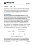
The function kill_x_cycles needs precise knowledge of instruction cycle timing. The function
was designed with known timings in mind, but verified in operation to ensure that it was
functioning properly. You can also use the simulator and observe the CCTIMER and CCSTEP
registers that show cumulative and last cycle instruction timings, respectively (see Figure 7.7.2).
Figure 7.7.2: Time-tracking registers
This screen capture shows the result of stepping over a call to the kill_x_cycles function with an
argument of 3 million. As you can see from the value in CCSTEP, the function is pretty close to
doing its job exactly.
With that, consider yourself properly ARMed to handle assembly language on the ARM7
processor. Though you could spend a lot of time writing assembler code and getting to know
the assembler more intimately, it is unlikely that you will write very much assembly language
for a 32-bit processor as it would just take too long. The LPC214x family of processors has
plenty of resources and power that even though you will probably have more bloated code by
writing in C, you will not run in to any problems where you will have wished you wrote a
program in assembler.
7.8 Welcome to the Real World
Perhaps the most interesting thing about an embedded system is the fact that it is a mechanism
to transform software to hardware. In all of the computer programming that you have done, it
is likely that the only output your programs had was to a monitor which, although often
entertaining, still has a strong feeling of “virtual” to it. In contrast, turning on an LED or a motor
or making sound in hardware that you have constructed is so much more tangible and
therefore “real” feeling. Warning: as soon as you get the hang of this, you are probably going
to want to make everything in your life automated by an embedded system!
It now becomes extremely important to understand the system schematics and how to line
them up to the firmware. So it is time to do a little hardware review. If you have not made a
hard copy of the development board schematics, now is the time to do it. From here until the
end of the course, you will be referring to the schematics continually as you write code to figure
out what signals are where, are they active high or active low, should they be driven directly or
notes_mpgl1_chapter7.docx
Release 1.0
Page 16 of 39
MPG LEVEL 1
operate as “open drain,” etc. The remainder of this chapter will focus on the processor symbol
itself, so it is shown here in Figure 7.8.1.1 with a bunch of detail removed so we can focus on
the relevant information we need.
Figure 7.8.1.1: Processor symbol showing just the input / output signal lines
All of the signal pins on a microcontroller are referred to as General Purpose Input Output
(GPIO). GPIO is a peripheral on a microcontroller that gives you access to the pins through
registers, just as we have already been introduced to early with the buttons. On this processor
and most others, output pins are grouped by “ports.” This means that the pins are named and
linked to registers in groups where their functionality is controlled. On the LPC214x, the I/O
notes_mpgl1_chapter7.docx
Release 1.0
Page 17 of 39
MPG LEVEL 1
pins will belong to either port 0 or port 1 and have a number such as P0.8. This means pin 8 of
port 0. Note that numbering starts at 0 (as long as they are all present) just like bit positions, so
P0.8 is in fact the ninth pin on its port. For the LPC214x, Port 0 has pins 0 thru 31 and Port 1 has
pins 16 thru 31.
As we look at processor registers that control functionality of the pins, the bits in the registers
correspond directly to the physical pins. For example, there is a port 0 register for reading the
logic state of the pin. The 9th bit in this port 0 register corresponds to P0.8, so if the value in the
register is 0x00000100, then you know that the signal on pin P0.8 is logic high and all the other
pins on that port are at logic 0.
7.8.1 GPIO Hardware
Before looking at all of the GPIO peripheral registers, let us look at the hardware that is
attached inside the processor to pretty much all of the pins. Unfortunately, the LPC214x
documentation does not have a diagram of the port pin hardware, so we will borrow one from
the LPC175x family (the processor used in MPG Level 2). Though it is not identical, it is nicely
illustrative (Figure 7.8.1.2).
Figure 7.8.1.2: GPIO hardware
Source: LPC175x Product Data Sheet, Philips Electronics (NXP)
notes_mpgl1_chapter7.docx
Release 1.0
Page 18 of 39
MPG LEVEL 1
The amount of logic might be surprising if you were expecting simple high and low logic – there
is definitely a lot more to it! We start from the right and work our way in.
1. PIN: the physical pin. You can see this, solder to it, and break it off if you are not careful.
The pin is held in place by the plastic case of the microcontroller, and come into the case
where very tiny bond wires attach to them and then get soldered onto the processor
silicon dye (see Figure 7.8.1.3).
Figure 7.8.1.3: Bond wires inside a chip
Source: VisionGauge Online, http://www.visionxinc.com/Applications/Wire-Bond-Inspection-andMeasurement.html, 2011-11-20
2. Next you see boxes marked ESD. These are ESD diodes built into the processor to help it
not get zapped. On a 3V MCU, the ESD diodes are probably set at around 5V and will
(hopefully) shunt any shock to ground so it does not fry your processor. In normal
operation, you do not even know they are there!
3. Then you hit a junction that divides the GPIO between input and output. These two
paths are connected together, but only one part of the hardware further upstream will
be active at any given time (sort of).
4. The output path is along the top and is fairly simple to understand. If you missed
learning about MOS transistors in Chapter 2, now is the time to read that.
notes_mpgl1_chapter7.docx
Release 1.0
Page 19 of 39
MPG LEVEL 1
Figure 7.8.1.4: Output driver on particular pin
5. The PMOS / NMOS pair form a CMOS pair (Complimentary MOS) that will drive the line
high or low depending on the data output value. Each pin has one of these drivers, and
the data output value comes from a particular bit in a particular register corresponding
to a particular pin that is set high or low. If you work out the logic, you can see that
“output enable” must be high to allow the “data output” signal to pass through and
drive the transistor pair. The “output enable” bit lives in a particular register and
corresponds to a particular pin. The “open-drain enable” line is connected only to the
top AND gate and thus only turns off/on the PMOS transistor in the CMOS pair. If you
have just an NMOS driver, you have an open-drain driver. Note that the ARM7 does
NOT have this configurable, though it has some permanent open-drain driven pins that
you need to watch out for.
6. The other path is the input path
Figure 7.8.1.5: Input driver on a particular pin
notes_mpgl1_chapter7.docx
Release 1.0
Page 20 of 39
MPG LEVEL 1
7. Starting at the bottom, there is a switch control line “select analog input” that activates
either the analog buffer (very bottom) or the digital Schmitt-trigger buffer. A pin cannot
be analog and digital at the same time. Some pins cannot be analog at all.
8. From the Schmitt-trigger, the logic signal is routed into “data input” that will set or clear
a particular bit in a particular register corresponding to a particular pin. The signal is
also fed back up and combined with a “repeater mode enable” signal – this is not
available on the LPC214x so we will not discuss it.
9. There are two more signal lines, “pull-up enable” and “pull-down enable” that drive a
so-called “weak” CMOS pair. These are better thought of as pull-x resistors with values
around 100k. They are great for signal conditioning of high-impedance input lines,
especially since they can be controlled by particular bits in particular registers
corresponding to particular pins. Unfortunately, the LPC214x family does not have this
feature, either. This is quite disappointing, actually, because a processor with this
feature is very handy, especially for unexpected signal drivers from external devices
where you suddenly need or do not need a pull-up or pull-down.
That is all the GPIO-specific configuration available on each pin. If you remember looking at the
processor diagram in Chapter 3, you should recall seeing that almost every pin had a bunch of
different functions. These alternate functions are configurations that come in addition to just
the GPIO configuration, though many of them will make use of the input or output drivers in
the GPIO hardware block. For example, the serial port peripheral has a transmit and receive
line. For transmitting, the peripheral must drive the pin high and low to communicate digital
data, so the peripheral will take control of the “data output” line. The peripheral receive line
will need to be a high impedance input so that it can be driven with receive data from whatever
device the processor is talking to. Therefore, the GPIO hardware will have to have the weak
pull-up and pull-down resistors turned off, and route the digital input information into the
serial peripheral.
The reason you need to know all of this is that you, the embedded programmer, must set up all
of the registers that control all of this configuration! This introduction should have given you a
good understanding about what you need to do, so now you get to learn how to do it.
7.8.2 Port Setup Registers
The hardware pins are mapped to port peripheral registers where the real signal can be read
and written. However, before you start reading and writing to pins, you have to set the pins up.
There are registers that set the pin function (i.e. to select which of the optional function you
want to use for the pin), and registers that set the data direction (either input or output) for the
pins. The first set of setup registers are summarized in Table 7.8.2.1. These include a
control/status register, function select registers, and data-direction registers. As we look
further into using the GPIO peripheral, we will find the specific details for all the bits within
each of these locations.
notes_mpgl1_chapter7.docx
Release 1.0
Page 21 of 39
MPG LEVEL 1
Table 7.8.2.1: Port I/O Setup - Related Registers
Address
(Hex)
Register Name
Symbol
System Control and
Status Flags register
SCS
0xE01F
C1A0
Bits 0 and 1 are set to enable high speed
GPIO access for port 0 and 1
respectively (a feature unique to the
latest family of LPC processors). All
other bits are reserved.
Pin function select
register 0
PINSEL0
0xE002
C000
Controls the function for the first 16
port 0 pins. Two bits are required for
each pin, where in general "00" means
primary function (GPIO), and "01", "10",
and "11" are the first, second and third
alternate functions, respectively. Table
60 in the LPC214x User Manual lists all
the functions.
Pin function select
register 1
PINSEL1
0xE002
C004
Controls the function for the last 16 port
0 pins. Table 61 in the LPC214x User
Manual lists all the functions.
Pin function select
register 2
PINSEL2
0xE002
C014
Controls the function for the port 1 pins.
Port 1 pins are not multiplexed
individually, so only two bits of PINSEL2
are used to configure all of the port 1
pins (see table 62 in the LPC214x User
Manual).
Port 0 Fast GPIO Port
Direction Control
Register
FIO0DIR
0x3FFF
C000
Port 0 data direction register. Each bit
corresponds to the pin number (i.e. bit 9
is for P0.9). Writing a 0 in the register
will make the corresponding bit an
input; writing a 1 will make it an output.
Port 1 Fast GPIO Port
Direction Control
Register
FIO1DIR
0x3FFF
C020
Port 1 data direction register. Each bit
corresponds to the pin number (i.e. bit
25 is for P1.25). Writing a 0 in the
register will make the corresponding bit
an input; writing a 1 will make it an
output.
notes_mpgl1_chapter7.docx
Function
Release 1.0
Page 22 of 39
MPG LEVEL 1
Manufacturers make an effort to name bits, pins, registers and peripherals with consistent and
descriptive names. Though the naming conventions might not be perfectly clear or intuitive at
first, and they are often quite different between manufacturers, once you have worked with a
family of processors for a while then you will start to understand the conventions which will
help to speed your development.
For example, the names of the two data direction control registers on the LPC214x start with an
“F” that denotes “fast.” The registers control IO for either port 0 or port 1. So the register
names are FIO0DIR and FIO1DIR -- Fast Input Output 0 Direction and Fast Input Output 1
Direction (where 0 and 1 are the respective ports). Here, “Fast” refers to a high-speed access
mode for the GPIOs that is unique to this ARM variant. If you look through the documentation
on GPIOs, you will also find regular IO0DIR and IO1DIR registers. These support legacy
functionality on older arm cores, so MPG will not pay any attention to the “regular mode” GPIO
registers and will only use the “fast mode” registers. In general, you always want to enable and
use the high speed GPIO access to the port registers. To tell the processor that we want to do
this, two bits are set in the SCS register. You can see this code in the Chapter 7 example
firmware. Beyond highlighting it here, you can pretty well forget about it.
MOV
LDR
STR
r0, #0x3
r1, =SCS
r0, [r1]
;
;
;
;
0xf0 in ROM: Grab literal for SCS setup
r1 = Address of SCS register (literal pool)
Set SCS to enable fast GPIO register access
for both Port 0 and Port 1
The pin function selection registers (PINSELx) control what each pin does based on the design
that you did for your project. The datasheet goes through each pin and tells you which bits
correspond to which pins and functions. Figure 7.8.2.1 shows an example from the datasheet
for the first two pins on Port 0.
Figure 7.8.2.1: Sample of Pin function selection guide from LPC214x datasheet
Source: LPC214x Product Data Sheet, Philips Electronics (NXP)
notes_mpgl1_chapter7.docx
Release 1.0
Page 23 of 39
MPG LEVEL 1
Look carefully at the mapping between the PINSEL bits and the pin functions. For Port 0 pins,
there are two bits that enable choosing one out of as many as four pin functions per pin. From
the Figure above, bits 0 and 1 in PINSEL0 configure pin P0.0. If both bits are 0, then the pin is
simply a basic GPIO. If the bits are 0 and 1, then the pin will be configured to operate as the
transmit pin for the UART0 peripheral. Setting 1 and 0 connect the pin to the PWM1
peripheral. Whenever a bit configuration is listed as “Reserved”, it should not be used (it may
or may not do anything) as is the case with setting both bits for this pin.
Port 1 is simpler because none of the pins have multiple functions or peripheral connections
(see Figure 7.8.2.2). However, the Port 1 pins are multiplexed with powerful debugging
functionality that can be optionally used in a circuit. Of course, your hardware would have to
be set up to support this. For the MPG development board, the JTAG debug port is used but
the TRACE functionality is not.
Figure 7.8.2.2: Port 1 PINSEL2 guide from LPC214x datasheet
Source: LPC214x Product Data Sheet, Philips Electronics (NXP)
If you look at the right-most column in the above two tables, you can see that the reset values
for the PINSEL registers are defined, which means that they are initialized in hardware for you.
Also notice that for the GPIO lines controlled by PINSEL0 and PINSEL1, “GPIO” mode is always
the default. Knowing this allows us to skip setting any PINSEL register for Chapter 7 because we
are not using any peripheral functions. Therefore, you will not see PINSEL configuration until
the C code structure is introduced next chapter.
The Direction Control Registers configure the port pins to be inputs or outputs. In the ARM
world, a ‘0’ corresponds to an input and a ‘1’ corresponds to an output. This may be a tad
counter-intuitive, but is not too hard to remember – just be careful if you start working on
several different processors where the logic might be backwards. For the Chapter 7 example,
we will only worry about the LEDs and buttons when considering the values we want to setup
for the DDR registers. This is safe as long as all the remaining value are kept as inputs to ensure
that the strong push-pull output drivers are not trying to drive signals from external circuits.
notes_mpgl1_chapter7.docx
Release 1.0
Page 24 of 39
MPG LEVEL 1
LEDs are outputs, and buttons are inputs, therefore define constants that will be loaded into
FIO0DIR and FIO1DIR to configure the IO direction:
PORT0DDR
PORT1DDR
EQU 0x00000000
EQU 0x01CF0000
; Keep port 0 entirely as inputs for now.
; b'0000 0001 1100 1111 0000 0000 0000 0000'
; Output pins on Port 0 (set = output)
Where did this information come from? The buttons are easy -- we have already seen in
section 7.3 how the schematics are used to identify what pins the buttons attach to, and thus
what bits their FIO0DIR bits correspond to. All of the buttons are on port 0, thus their
input/output direction control will be set by FIO0DIR so the constant PORT0DDR is configured
for all inputs (we do not care what the other signals attached to port 0 is for now). The Figure is
repeated here (Figure 7.8.2.3):
Figure 7.8.2.3: Portion of processor schematic showing button inputs
The LEDs are slightly different. Figure 7.8.2.4 shows the relevant part of the schematic.
Figure 7.8.2.4: LEDs from the schematics
So the LEDs appear on both port 0 and port 1. For the example code, we are not going to
configure the DDR values for the purple and white LEDs on port 0 (this is left as part of the
chapter exercise). We will only set up the outputs on port 1. From Figure 7.8.2.4, the red LED is
on P1.16 and thus setting bit 16 of FIO1PIN will configure the pin to be an output and allow the
LED to be toggled on and off. Mapping the other LEDs is done in exactly the same way. The
result is the value for PORT1DDR, where bits are set for each of the six port 1 LEDs. It is easy to
see this in the binary notation as shown in the comment, but it is more practical to convert that
to hex (though you can do either in the assembler environment). C does not allow binary
numbers, so you will be forced to write in hex but it never hurts to write a binary comment to
help yourself out. With the PINSEL and FIOxDIR registers set up correctly, you can start using
the port pins in basic GPIO mode.
notes_mpgl1_chapter7.docx
Release 1.0
Page 25 of 39
MPG LEVEL 1
7.8.3 Port Access Registers
The second set of registers to discuss are those that allow you to read, set and clear the GPIOs.
These are shown in table 7.8.3.1.
Table 7.8.3.1: GPIO Access Registers
Address
(Hex)
Function
FIO0MASK
0x3FFF
C010
Port 0: Clear bits open control of set and
clear functions to corresponding pins.
Port 1 mask register
FIO1MASK
0x3FFF
C030
Port 1: Clear bits open control of set and
clear functions to corresponding pins.
Port 0 bit set register
FIO0SET
0x3FFF
C018
Port 0: Write ones to bits to set the
corresponding pin high as long as
corresponding bit in the FIO0MASK
register is set.
Port 1 bit set register
FIO1SET
0x3FFF
C038
Port 1: Write ones to bits to set the
corresponding pin high as long as
corresponding bit in the FIO1MASK
register is set.
Port 0 bit clear register
FIO0CLR
0x3FFF
C01C
Port 0: Write ones to bits to clear the
corresponding pin (make low) as long as
the corresponding bit in the FIO0MASK
register is set.
Port 1 bit clear register
FIO1CLR
0x3FFF
C03C
Port 1: Write ones to bits to clear the
corresponding pin (make low) as long as
the corresponding bit in the FIO1MASK
register is set.
Port 0 state register
FIO0PIN
0x3FFF
C014
Port 0: Read this register to get the
current state of the port; write to this
register to change the state of the
corresponding pins.
Port 1 state register
FIO1PIN
0x3FFF
C034
Port 1: Read this register to get the
current state of the port; write to this
register to change the state of the
corresponding pins.
Register Name
Symbol
Port 0 mask register
notes_mpgl1_chapter7.docx
Release 1.0
Page 26 of 39
MPG LEVEL 1
Again, all the registers described here are the “fast access” variants so they all start with “F”. In
most cases, the register name tells you what each one of them does, and the Function
description tells you how.
Reading the logic signal levels present on the pins in a port is accomplished by reading the pin
state registers, FIO0PIN and FIO1PIN. Simply perform a load instruction with the register
address as the source address, and you will get a snapshot of the current value on the pins. In
assembly, it looks like this:
LDR
STR
r1, =FIO0PIN ; Load r1 with address of FIO0DIR (literal pool)
r0, [r1],
; Read the values in FIO0PIN to r0
In C, it is even easier:
u32 u32PortValue;
u32PortValue = FIO0PIN;
The symbol FIO0PIN is set up in the C header file for the processor in a way that makes this
notation possible, even though technically you are dereferencing a pointer to the address of
FIO0PIN to get the contents. You can find out what the address of the FIO0PIN register from
the processor data sheet and address it explicitly if you want to!
The value that appears in your destination register is a bunch of bits that correspond to
particular pins (in this case on port 0). Bit 0 is the logic level of port 0, pin 0 which is denoted
P0.0. Bit 1 is the logic level of P0.1. The MSB in the register, bit 31, is the logic level of the pin
at P0.31. For example, if all 32 port 0 pins were inputs, P0.0 to P0.15 were at Vss (0V), and P16
to P0.31 were at Vdd (3.3V), then reading FIO0PIN would put the value 0xFFFF0000 into your
destination register. If there is ANY confusion about that, you need to figure it out before
moving on. A good way to do this is to step through the Chapter 7 code running on your
development board and look at the FIO0PIN register as you press and release the different
buttons. You should see the bits changing in the register. If you put a break point on the line of
code that reads the FIO0PIN register, then there should be no surprise at what appears in r3.
update_LED
LDR
r3, [r2]
; r3 = *r2 read the current FIO0PIN value
Once you have the data snapshot, you can do whatever you want with it such as checking if an
input button is high or low. Note that the logic values on the pins configured as outputs will
also be part of the data that is read when you access FIO0PIN.
You can also write to the FIOxPIN registers to change the state of the pins that are configured
as outputs. If you do this, you must first read the current value of the register into a temporary
register, change only the bits you want to change with AND, OR, or BIC operations, then write
the value back out. Writing to FIOxPIN updates ALL of the bits in the register, so if you
inadvertently change bits that you do not want to change while manipulating the ones you do
notes_mpgl1_chapter7.docx
Release 1.0
Page 27 of 39
MPG LEVEL 1
want to update, you will have some interesting errors when you write the value back onto the
port. Even if you wanted to set just one bit, you will need a bunch of instructions to read,
modify, and then write the register value back so you do not destroy the other bits.
Aside from being risky, port writes through FIOxPIN registers are quite inefficient and on some
processors can be an outright problem due to the somewhat infamous “read-modify-write”
problem (if you ever program with PIC processors, you better understand this issue!). Most
processors do not have problems related to this, but it is still a cumbersome way to change bits
in an output register.
The best way to write to pins is with the SET and CLEAR (CLR) registers. These cause writes to
the output latch registers directly and will only impact the bits you want to write. Writing a 1 to
a bit in a SET register will force the corresponding pin to be set (as long as the pin is configured
as an output). Writing a 0 to the SET register does nothing. Writing a 1 (yes, you write a one)
to a bit in a CLR register will force the corresponding bit low (again, as long as the data direction
register agrees). Writing a 0 to a CLR register does nothing. You do not have to read the output
register first. There is an example of all of this in a few paragraphs.
The LPC214x processors have some protection bits that can help you lock off access to
particular pins. The bits are in the register FIOxMASK. The MASK register is used in conjunction
with an FIOxPIN, FIOxSET or FIOxCLR access. Only bits that are 0 in the MASK register will be
allowed to change, so the chance of erroneously changing a locked bit is slim. If you ever build
an embedded system where one of the IO lines toggles the power switch to a life-support
machine, you might want to unmask that bit once you turn it on!
To drive all this home, here is some pseudo C code to setup the LPC214x for a fantasy board
that has 16 inputs on P0.0 – P0.15 and 16 outputs on P0.16 – P0.31. The outputs are changed
by writing directly to FIO0PIN and also by using FIO0SET.
u32 u32Temp = 0;
SCS |= 0x00000003;
PINSEL0 = 0;
PINSEL1 = 0;
FIO0DIR = 0xFFFF0000;
FIO0SET = 0xFFFF0000;
FIO0MASK = 0x5555FFFF;
u32Temp = FIO0PIN;
FIO0PIN &= 0x00000000;
u32Temp = FIO0PIN;
/*
/*
/*
/*
/*
/*
/*
/*
/*
Set bits 0 and 1 to enable Fast register access */
Set all port 0 pins to GPIO mode */
Set all port 1 pins to GPIO mode */
Set P0.0–P0.15 to inputs, P0.16–P0.31 to outputs */
Set all pins P0.16 – P0.31 to logic high */
Mask allows access only to P0.31, P0.29, … P0.17 */
u32Temp = 0xFFFFXXXX (X = unknown inputs)*/
Clear pins P0.31, P0.29, … P0.17 (uses MASK) */
u32Temp = 0x5555XXXX (X = unknown inputs)*/
A big difference between using SET and CLEAR registers vs. FIOxPIN registers is how you write
code to access them in C. Although the difference might appear subtle, it is very different and
is a very hard bug to catch. You always write directly to SET and CLEAR registers to make things
happen, whereas you always perform a read-modify-write operation when using PIN registers.
For example, if you had a bit mask to turn on and turn off a bunch of LEDs on port 0, you could
do it with FIO0PIN accesses, or FIO0SET and FIO0CLR:
notes_mpgl1_chapter7.docx
Release 1.0
Page 28 of 39
MPG LEVEL 1
#define
LED_MASK
0x01C70000
/* LED bit positions */
/* Set LEDs on with FIO0PIN*/
FIO0PIN |= LED_MASK; /* Becomes many lines of asm to read-modify-write */
/* Turn LEDs off with FIO0PIN */
FIO0PIN &= ~LED_MASK; /* Many lines of assembler! */
/* Set LEDs on with FIO0SET */
FIO0SET = LED_MASK; /* This should be just three lines of code */
/* Turn LEDs off with FIO0CLR */
FIO0CLR = LED_MASK; /* Three lines of asm code */
Even though both methods require only one line of C code, the assembly language and resulting
instruction cycles that the compiler must write to carry out those operations is substantially
more for the FIO0PIN accesses. Note that when you want to change bits in FIO0PIN, you must
use |= or &= which should give you a clue as to the assembly language that will be written. The
current value of FIO0PIN must be read, then bit-wise ORed or ANDed, then written back. The
clear the bits of interest, the inverted LED_MASK value is ANDed to FIO0PIN (~ flips all bits in a
literal – this is pre-processor so this does not cost any instruction cycles, but you will have to
store the inverted literal as a constant in flash somewhere unless it can be created by the
immediate generator). With FIO0SET and FIO0CLR, you assign LED_MASK directly to the
SET/CLR register so there is only a write, and no read or modify instructions. You also use the
same LED_MASK value for both setting and clearing. This is very smartly done because only
one flash location is required to store LED_MASK since it is not inverted.
The moral of this story: always you SET and CLR registers if they are available. On that note,
only some register provide SET and CLR access, so you cannot just randomly pick a register
name and through SET or CLR in the name and expect it to work. You will come across them in
several other peripherals that will be used in the course.
7.9 Program Exploration
Now we can look at the complete Chapter 7 example source code to make sure you fully
understand everything to this point. Open the workspace and load the “start” code for
Chapter 7. You should see three assembler source files:
1. chapter7.s
2. cstartup.s
3. devboardasm.s
The processor header file and linker file are also added to the project.
notes_mpgl1_chapter7.docx
Release 1.0
Page 29 of 39
MPG LEVEL 1
7.9.1 cstartup.s
There has been plenty of discussion about cstartup.s and the code it contains. There is no
custom setup code in this file, so we will not worry about it very much. The key thing this file
does is set the various address vectors for system functions. A “vector” is merely a fancy name
for an address.
__vector:
LDR
LDR
LDR
LDR
LDR
__vector_0x14:
DC32
LDR
LDR
PC,Reset_Addr
PC,Undefined_Addr
PC,SWI_Addr
PC,Prefetch_Addr
PC,Abort_Addr
;
;
;
;
;
Reset
Undefined instructions
Software interrupt (SWI/SVC)
Prefetch abort
Data abort
0
PC,IRQ_Addr
PC,FIQ_Addr
; RESERVED
; IRQ
; FIQ
; The symbols used above are defined here.
; the function addresses are on the right.
DATA
Reset_Addr:
Undefined_Addr:
SWI_Addr:
Prefetch_Addr:
Abort_Addr:
IRQ_Addr:
FIQ_Addr:
DCD
DCD
DCD
DCD
DCD
DCD
DCD
The symbol name is on the left,
__iar_program_start
Undefined_Handler
SWI_Handler
Prefetch_Handler
Abort_Handler
IRQ_Handler
FIQ_Handler
What that really means is that these labels translate into addresses that are stored at particular
memory locations where the processor hardware will go to seek an address at a critical time.
Mnemonics are used like this to allow easy reallocation of the handler functions because their
location in flash will change whenever code is added to the program. The easiest example is
the Reset vector which has the mnemonic Reset_Addr in the file. Look around line 66 of
cstartup.s:
Reset_Addr:
DCD
__iar_program_start
This is not actually a line of code, but an assembler command that puts the value of the
__iar_program_start symbol (which is the address of the first line of code in the program and
happens to be 0xb4) at the memory location Reset_Addr (which happens to be 0x20). If you
look at the very start of the disassembly window when you start the debugger, you should be
able to find these values – another great exercise to try! Figure 7.9.1.1 shows you a snapshot of
the Disassembly window where you can see all of these symbols. Make sure you can find all of
the numbers to better understand what this window shows you.
notes_mpgl1_chapter7.docx
Release 1.0
Page 30 of 39
MPG LEVEL 1
Figure 7.9.1.1: Disassembly window showing all of the symbols
All of these instructions load the Program Counter with certain addresses and will execute if the
program counter gets there. How does the program counter get there if it jumps over the code
due to the reset vector? Just like hardware ensures that the first instruction read on the
processor is at address 0x0000, hardware will load one of these vectors under special
circumstances in processor operation. These are called “events” or “exceptions” which are
detected by the processor hardware logic. There are only a few types of events that can occur,
so the MCU has logic to look up a hard-coded value to load into the program counter so the
processor will branch to that vector. The 7 events have exactly 7 vectors, and the processor will
always branch to those addresses. As soon as the program counter is there, it get reloaded to
the current address of the function handler for that particular exception.
Since we love talking about interrupts before ever explaining them, we might as well use the
IRQ event as an example. If a low priority interrupt (IRQ) occurs, the hardware will detect this
and automatically load the program counter with the address of the IRQ vector which is 0x14.
So the program counter winds up on the line of code which contains the instruction:
LDR
PC,IRQ_Addr
; IRQ
When the firmware was built, the symbol for IRQ_Addr was defined (called IRQ_Handler) and is
the location in flash of the function to handle the IRQ. This address is loaded to the program
counter so the processor branches to IRQ_Handler to execute the appropriate code. This twobranch maneuver is necessary because the address of IRQ_Handler will change with each build,
and the hardware to detect an exception and vector the program counter must have a static
address.
Right now, all the code does is trap the program so whatever is broken cannot cause even more
trouble (a processor running wild is a dangerous thing sometimes). This instruction “B .” simply
continually loads the program counter with the address of itself (think of the B . instruction as
notes_mpgl1_chapter7.docx
Release 1.0
Page 31 of 39
MPG LEVEL 1
while(1); ). Remember, an embedded processor is somewhat ruthless in that it will keep
pointing through memory and trying to execute anything that the program counter is pointing
at regardless if it is a valid instruction or not. If your program winds up in a place where it
should not be, at least if you can trap it there it will not start doing crazy things. While getting
stuck does not do anything useful as far as a user goes, it should be obvious to you that
something is wrong and with debug access to the code you can start to figure out what went
wrong.
In this particular program, we do not expect any interrupts to occur, therefore the trap is useful
because if the program ever did get there, we could see that in the debugger and then figure
out what bug caused that erroneous jump to IRQ_Handler. In the future, our programs will use
interrupts and instead of trapping the processor with a B . instruction, we will add an interrupt
service function that will execute whenever the interrupt occurs and the processor vectors to
IRQ_Handler. Stay tuned!
7.9.2 Map File and Symbol Table
This is a great time to introduce the .map file that is created when you build your code. If you
cannot find this file in the Output folder, make sure that “Generate linker map file” is enabled
inside Project Options > Linker > List. Build the code and the file should appear (Figure 7.9.2.1).
Figure 7.9.2.1: Debug window showing .map file with the symbol list
notes_mpgl1_chapter7.docx
Release 1.0
Page 32 of 39
MPG LEVEL 1
The .map file is a summary of all of the objects, symbols, code sections, etc. that the Linker is
aware of in putting together the final binary file that will be flashed to your processor. Not only
can this be a powerful debugging tool, it is generally informative in that it tells you what
resources all of the different parts of your program are using. Below is the summary from the
file for Chapter 7.
*****************************************************************************
*** MODULE SUMMARY
Module
ro code
-----------D:\MPG\MPG Level 1\Firmware\Chapter 7 Assembler GPIO\Debug\Obj: [1]
chapter7.o
112
cstartup.o
132
devboardasm.o
24
---------------------Total:
268
The three source files take up a total of 268 bytes of flash memory even though this program
barely does anything (ro = read-only code i.e. flash). If you have worked on simple 8-bit micros
like PICs that sometimes only have 1k or 2k of flash, consuming 25% of that for startup code
and a little light blinking probably seems like a lot. Perhaps the appropriate proverb at this time
is that to fire a bigger bullet, you need a bigger gun. A complicated 32-bit embedded system
will indeed take more memory to initialize and get started. And of course, every line of
assembly code in a 32-bit system requires 4 bytes of memory. To confirm this, notice that
devboardasm.o uses 24 bytes – take a look at the source code and see that there are six
instructions for the function and of course 6 instructions x 4 bytes / instruction = 24 bytes.
As your programs get more complicated, your resource usage will indeed rise as well. If doing
nothing costs 268 bytes, then doing something must cost infinite bytes! That of course is not
true. What you will see as you write more complicated firmware is that there is almost a
standard amount of memory usage involved with any new object file, but the file will grow
more slowly than you might expect even as you add complex code. Startup code is brute force
and takes space. Clever solutions to problems with careful thought and good coding practices
will likely not grow in size as quickly as you might think.
The .map file will also show you RAM usage when your source files start declaring variables. All
of this becomes critically important when you try to build code and are told that the sum of all
of your parts exceed the available resources! Embedded designers do not like this message,
but guaranteed you will see it. Having the .map file available to see what pieces of code are
perhaps hogging all the memory can help you target efforts to shrink your code and make it fit.
One of the most frustrating things is running out of code space, especially if you are just fixing a
quick bug on a released product!
notes_mpgl1_chapter7.docx
Release 1.0
Page 33 of 39
MPG LEVEL 1
7.9.3 chapter7.s
If you are getting worried that there has been a great deal of discussion about fairly confusing
program counters bouncing around even though the program has done nothing but reset, fear
not! The rest of the code does things that are much more tangible and hopefully are easier to
grasp. Open up chapter7.s and scroll down to around line 26.
Constants are defined in assembly programs just like in C. For symbol definitions, EQU is
typically used. These are values that may or may not be “generatable” by the literal generator
but at this time we will not worry about it – we just want meaningful names for numbers.
When we use these values we will need to be cognizant of what they are. It was mentioned
earlier that any value that cannot be generated will be stored in flash in a “literal pool” – a
section of ROM that will hold the numbers so they can be retrieved with an LDR instruction.
The location of the literal pool will be decided by the assembler and linker.
The chapter7.s files has an include section that can associate files with pre-processor definitions
just like in C. Including iolpc214x.h gives our source file access to all the predefined names for
registers and bits.
Pay attention to the source code that shows how the values must be loaded into a register. If
the number can be generated by immediate generator, then use a MOV instruction and the
immediate is preceded with a hash:
MOV
r0, #0x3
; 0x0044 in ROM: Grab literal for SCS setup
If you look at this in the disassembly window, then you see that the instruction is pretty much
there verbatim from what you typed (see Figure 7.9.3.1). By the way, what address is this
instruction at in flash?
Figure 7.9.3.1: MOV literal instruction in the disassembler
If the number you want to load cannot be created from the immediate generator, then it must
be loaded from the literal pool with an LDR instruction. The symbol SCS is a value from the
processor’s header file and is equal to 0xE01FC1A0 (the address of the SCS register). When the
code is built, the assembler automatically stores 0xE01FC1A0 in a memory location (the literal
pool), then updates this instruction to be able to access it. Every module has a literal pool and
it is stored at the end of the module code in flash. The value is obtained by loading an offset to
the program counter to reach the literal pool (and as long as the module is not larger than 4kB,
this works). Take a look at Figure 7.9.3.2.
notes_mpgl1_chapter7.docx
Release 1.0
Page 34 of 39
MPG LEVEL 1
Figure 7.9.3.2: Translation of the LDR and the literal pool location
Remember that the line in light gray at the top is the line of assembly code that was written in
chapter7.s:
LDR
r1, =SCS
; r1 = Address of SCS register (literal pool)
But this is not exactly the instruction that is stored in flash. The line beneath it highlighted in
green by the program counter is the actual instruction that is stored at address 0x48.
LDR
r1, _?0 [0xa0]
; SCS
The “=SCS” has been replaced by the symbol “_?0” which is sequentially generated by the
assembler (you will see _?1, _?2, etc. later on). You are even told what the value of the symbol
is so you can go look at it if you want. If you scroll down in the disassembly window to address
0xa0, you see the value in flash and the DCD association to the symbol name SCS:
_?0:
0xa0: 0xe01fc1a0
DCD
SCS
The program counter does not actually jump to the literal pool location – it just uses its current
value and the offset as a pointer to fetch the value at that memory location and bring it in to
R1. The process is fairly straightforward once you understand what the assembler is doing and
how the program must work to get the numbers you need.
Once the SCS register is loaded, we can initialize the GPIO peripheral values to configure the
input and output direction registers for the example code. The program is very simple and will
only make use of a few LEDs and a button. The goal will be to have the blue LED blinking at
about 2 Hz and the yellow LED will turn on if BUTTON0 is pressed. Since we are only using GPIO
functions, there is no need to configure any PINSEL register because they always default to
GPIO function for all pins. You can verify that by selecting “Pin connect block” inside a Register
window if you are running the debugger (see Figure 7.9.3.3).
notes_mpgl1_chapter7.docx
Release 1.0
Page 35 of 39
MPG LEVEL 1
Figure 7.9.3.3: PINSEL registers: all GPIO functions are active
The next lines of code setup FIO0DIR and FIO1DIR using the constants that have been defined
with bits corresponding to the LEDs and buttons of interest to correctly configure them as
outputs and inputs.
LDR
LDR
STR
r0, =PORT0DDR
r1, =FIO0DIR
r0, [r1], #0x14
; Load r0 with the constant (literal pool)
; Load r1 with address of FIO0DIR (literal pool)
; *r1 = r0; r1 += 20 and now points to FIO0PIN.
LDR
LDR
STR
r0, =PORT1DDR
r2, =FIO1DIR
r0, [r2], #0x14
; Load r0 with the constant (literal pool)
; Load r2 with address of FIO1DIR (literal pool)
; *r2 = r0; r2 += 20 and now points to FIO1PIN
MOV
STR
r0, #P1_START
r0, [r2]
; r0 = starting value for port 1 (immediate)
; *r2 = r0 to turn all LEDs off
Since this program has only one purpose and is not interrupted by any other source, we will
allocate some core registers to hold values that will be used throughout the main program loop.
That way there will not be any need to reload registers with peripheral addresses that will
waste processor cycles and flash space. The designated use of the registers are described in the
code:
;
;
;
;
;
r0
r1
r2
r3
r4
holds the number of cycles to call the function with
already points to FIO0PIN to read and write the port 0 GPIO
already points to FIO1PIN to read and write the port 1 GPIO
will be a working register for LEDs
will be a working register for buttons
Registers r3 and r4 will not have the same value all of the time and will be used like temp
registers for data storage and manipulation as required.
Once main starts, there is hardly any code that makes the program do what it does. Even
though this is written in assembler, you should be pretty comfortable understanding what is
going on just by reading the labels and comments. If we wrote this in C it would like something
like:
u32 u32CyclesToKill = 3000000;
u32 u32Temp;
notes_mpgl1_chapter7.docx
Release 1.0
Page 36 of 39
MPG LEVEL 1
while(1)
{
/* Kill time between blinks */
kill_x_cycles(u32CyclesToKill);
/* Get the current LED state and toggle the blue LED bit */
u32Temp = FIO1PIN;
u32Temp ^= LED_BLU;
/* Check for button press – button is active-low */
if( !(FIO0PIN & BUTTON0_MASK) )
{
/* If button logic is low, button is pressed so turn light on */
u32Temp |= LED_YLW;
}
else
{
/* else button logic is high so button is released and light is off */
u32Temp &= ~LED_YLW;
}
/* Write the updated LEDs to the output port */
FIO1PIN = u32Temp;
} /* end while */
Other than the FIOxPIN accesses, this code should be absolutely trivial. This is a great example
because the assembly language matches the C language very closely. Almost every line of C
translates directly into a line of assembler, and the structures and actions taking place are quite
similar, too. Check it out in assembler:
main_loop
LDR
r0, =KILL_CYCLES
BL
kill_x_cycles
; r0 = cycles to kill
; Branch and Link for function call; watch r14!
update_LED
LDR
r3, [r2]
EOR
r3, r3, #LED_BLU
; r3 = *r2 read the current FIO1PIN value
; r3 = r3 XOR the value to toggle the blue LED
check_button
LDR
r4, [r1]
ANDS r4, r4, #BUTTON0_MASK
BNE
button_not_pressed
; r4 = *r1 read the current FIO0PIN value
; Mask off all bits except BUTTON0
; if (BUTTON0)
button_pressed
ORR
r3, r3, #LED_YLW
B
continue
; Turn on the yellow LED bit in r3
; Jump around the other case to continue
button_not_pressed
BIC
r3, r3, #LED_YLW
; Clear the yellow LED bit
; Simply flow into "continue"
continue
notes_mpgl1_chapter7.docx
Release 1.0
Page 37 of 39
MPG LEVEL 1
STR
r3, [r2]
; Write the modified value back to port 0
B
main_loop
; Repeat infinitely
Not a lot more can be said to explain what happens. The function call to kill_x_cycles has
already been discussed in section 7.4 on FOR loops. Between every blink of the LED,
kill_x_cycles causes about three MILLION clock ticks to go by while it simply sits there burning
power. This is a brute-force way of making time pass, and it would be very rare to use a
technique like this to kill time in a meaningful embedded system. Aside from the waste of
power, there are plenty of other problems with this approach, one of which you should notice
as soon as you run the program and start pressing the button. However, it is great for being
quick and easy. By the way, single-stepping through kill_x_cycles is not a great idea unless you
drastically reduce the argument passed in to it – something that might be useful for testing
functions in the future. Make use of “Step Over” and break points. If you right-click on a line of
code, there will be an option to set breakpoints and an option to “run to cursor” which does
exactly that.
Run through this code until you understand everything. Find all of the GPIO registers that are
used and make sure you see the values changing in the debugger windows. You can even edit
the register values directly to make LEDs go on manually. You probably now know more
assembler than many embedded engineers that use ARM processors. Keep a look out for
instances where you make use of this low level knowledge and be thankful that you have put
the effort in to learn it when it helps you out.
7.10 Chapter Exercise
All chapters in MPG Level 1 from this point on have exercises to allow you to prove that you
have learned the chapter material. Exercises will always indicate what skills they are testing
and therefore what knowledge you should have at this point in the course. The firmware you
need is in the “start” section of the web page firmware for this chapter. The solution is posted
in the “end” section.
7.10.1 Skills tested
•
•
•
•
•
Use ARM7 assembly language
IAR debugger environment
Translation of physical pins to logical GPIO peripheral i.e. pin mapping
Reading and writing GPIO peripheral registers to configure and use the peripheral
Also be sure you see and understand the following:
o The difference between generated literals and numbers that are looked up from
the literal pool.
o How the GPIO registers get set up to access the buttons and LEDs
o How the button inputs are read
o How it is determined that a button is pressed
o How the program counter is moved depending on the input conditions
notes_mpgl1_chapter7.docx
Release 1.0
Page 38 of 39
MPG LEVEL 1
o How the LEDs are turned on
o How the program works forever.
7.10.2 Exercises
1.
2.
3.
4.
Turn the green and orange LEDs on at the start of the code and keep them on
Add blinking of the red LED opposite to the blue LED.
Turn on the white and purple LEDs if BUTTON1 is pressed
Make the Cyan LED blink twice as fast as the others while maintaining all other
functionality
5. Make BUTTON3 toggle the state of the green and orange LED (i.e. they start on and turn
off with the first press of BUTTON3; they turn back on with the second press of
BUTTON3). Use SET and CLR registers.
notes_mpgl1_chapter7.docx
Release 1.0
Page 39 of 39