1
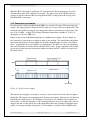
PSI System Controls and Diagnostics
General I/O
Analog
I/O (3+2)
Ch0
LP
filter
I-V conv
Ch1-128
Digital
I/O
(4+4)
+5V
+24V
Optoisol
Relay
MUX
LP
filter
Gated int
Current
switches
ADCs
Actuator control
Reset
Current
source 1
Fiber optic board
+2.5V
Current
source 2
A60
FPGA
LEDs
(x32)
ADAS board
ADAS
electrometer
chip
(x32)
(x32)
Mode and
address
NIOS
core
NIOS
core
FPGA
: : : : Jpr
: : : : banks
Serial
TxRx
(x32)
Memory
Gate in
Ethernet
TxRx
+15V,+/-12V, +/-5V,
+3.3V, +2.5V, +1.2V
DACs
Gate out
Mon out
Setpoint
HV PSU
(optional)
CPLD
CPLD
HV on LED
Enable
Ethernet
Safety
relay
UUUU
HV out
HV sense
Relay
Opto
Fuse 1.1A
Mode
keyswitch
UUUU
HV loopback
Enable
DC-DC
converters &
regulators
Relay
HV sense
Relay
RS-232/485
Enabled
Interlock
+24VDC in
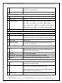
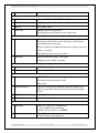
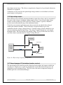
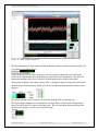
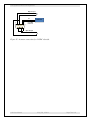
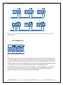
Figure 37. I128 block schematic.
12.2.2 Calibration current switching
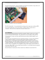
A matrix of switches allows the currents generated by the two precision calibration current
sources to be routed to the required signal input under software control.
12.2.3 Analog signals
The multichannel ADC also reads the two high voltage signals formed by voltage division, and
the general purpose analog inputs. Three differential analog inputs are provided on the I/O
connector; two of them are switched by a multiplexer (MUX) into one ADC input.
A multichannel DAC (digital to analog converter) provides the setpoint for the high voltage and
the two general purpose analog outputs. All analog inputs and outputs are buffered, the inputs
are also low-pass filtered with -3dB at 35 kHz.
12.2.4 Digital signals
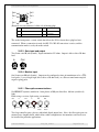
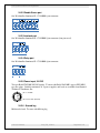
The general purpose digital lines on the I/O connector are all buffered. The TTL digital inputs
are active low, with 50 kohm pull up to +5V. Two of the inputs are read by the A60 and two by
the secondary FPGA. The two opto isolated inputs on the actuator connector, typically “actuator
in” and “Actuator out” are read by the A60.
I128 User Manual
I128_UM_141014
Page 62 of 121