1
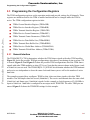
DatasheetDirect.com
Your dedicated source for free downloadable datasheets.
Over one million datasheets
Optimized search function
Rapid quote option
Free unlimited downloads
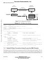
Visit www.datasheetdirect.com to get your free datasheets.
This datasheet has been downloaded by http://www.datasheetdirect.com/
Freescale Semiconductor, Inc...
Freescale Semiconductor, Inc.
MSC8102 User’s Guide
16-Bit Digital Signal Processor
MSC8102UG/D
Rev 0, 3/2003
For More Information On This Product,
Go to: www.freescale.com
Freescale Semiconductor, Inc...
Freescale Semiconductor, Inc.
HOW TO REACH US:
USA / EUROPE / Locations Not Listed:
Motorola Literature Distribution
P.O. Box 5405
Denver, Colorado 80217
1-800-521-6274 or 480-768-2130
JAPAN:
Motorola Japan Ltd.
SPS, Technical Information Center
3-20-1, Minami-Azabu Minato-ku
Tokyo 106-8573 Japan
81-3-3440-3569
ASIA/PACIFIC:
Motorola Semiconductors H.K. Ltd.
Silicon Harbour Centre
2 Dai King Street
Tai Po Industrial Estate,
Tai Po, N.T., Hong Kong
852-26668334
HOME PAGE:
http://motorola.com/semiconductors/
Information in this document is provided solely to enable system and software implementers to use
Motorola products. There are no express or implied copyright licenses granted hereunder to design or
fabricate any integrated circuits or integrated circuits based on the information in this document.
Motorola reserves the right to make changes without further notice to any products herein. Motorola
makes no warranty, representation or guarantee regarding the suitability of its products for any
particular purpose, nor does Motorola assume any liability arising out of the application or use of any
product or circuit, and specifically disclaims any and all liability, including without limitation
consequential or incidental damages. “Typical” parameters that may be provided in Motorola data
sheets and/or specifications can and do vary in different applications and actual performance may
vary over time. All operating parameters, including “Typicals” must be validated for each customer
application by customer’s technical experts. Motorola does not convey any license under its patent
rights nor the rights of others. Motorola products are not designed, intended, or authorized for use as
components in systems intended for surgical implant into the body, or other applications intended to
support or sustain life, or for any other application in which the failure of the Motorola product could
create a situation where personal injury or death may occur. Should Buyer purchase or use Motorola
products for any such unintended or unauthorized application, Buyer shall indemnify and hold
Motorola and its officers, employees, subsidiaries, affiliates, and distributors harmless against all
claims, costs, damages, and expenses, and reasonable attorney fees arising out of, directly or
indirectly, any claim of personal injury or death associated with such unintended or unauthorized use,
even if such claim alleges that Motorola was negligent regarding the design or manufacture of the part.
MOTOROLA and the Stylized M Logo are registered in the U.S. Patent and Trademark Office. OnCE
and digital dna are trademarks of Motorola, Inc. All other product or service names are the property
of their respective owners. Motorola, Inc. is an Equal Opportunity/Affirmative Action Employer.
© Motorola, Inc. 2002, 2003
MSC8102UG/D
For More Information On This Product,
Go to: www.freescale.com
Freescale Semiconductor, Inc...
Freescale Semiconductor, Inc.
MSC8102 Overview
1
Configuring Reset, Boot, and Clock
2
Managing Internal Memory
3
Connecting to External Memory
4
Interrupt Programming
5
Managing the Buses
6
Using the DMA Channels
7
Direct Slave Interface Programming
8
Setting Up for Time-Division Multiplexing
9
System-Level Debugging
10
Configuring the Timers
11
Managing Shared Resources
12
MSC8102 Dictionary
A
Connecting the DSI in Various Endian Modes
B
Connecting Processors to the DSI
C
Sliding Window Addressing Guidelines
D
Index
For More Information On This Product,
Go to: www.freescale.com
IND
Freescale Semiconductor, Inc...
Freescale Semiconductor, Inc.
1
MSC8102 Overview
2
Configuring Reset, Boot, and Clock
3
Managing Internal Memory
4
Connecting to External Memory
5
Interrupt Programming
6
Managing the Buses
7
Using the DMA Channels
8
Direct Slave Interface Programming
9
Setting Up for Time-Division Multiplexing
10
System-Level Debugging
11
Configuring the Timers
12
Managing Shared Resources
A
MSC8102 Dictionary
B
Connecting the DSI in Various Endian Modes
C
Connecting Processors to the DSI
D
Sliding Window Addressing Guidelines
IND
Index
For More Information On This Product,
Go to: www.freescale.com
Freescale Semiconductor, Inc.
Contents
Freescale Semiconductor, Inc...
About This Book
Before Using This Manual—Important Note . . . . . . . . . . . . . . . . . . . . . . . . . . . . . . . . . . . . . . . . xviii
Audience and Helpful Hints . . . . . . . . . . . . . . . . . . . . . . . . . . . . . . . . . . . . . . . . . . . . . . . . . . . . . xviii
Notational Conventions and Definitions . . . . . . . . . . . . . . . . . . . . . . . . . . . . . . . . . . . . . . . . . . . . xviii
Organization . . . . . . . . . . . . . . . . . . . . . . . . . . . . . . . . . . . . . . . . . . . . . . . . . . . . . . . . . . . . . . . . . . xix
Other MSC8102 Documentation . . . . . . . . . . . . . . . . . . . . . . . . . . . . . . . . . . . . . . . . . . . . . . . . . . xxi
Further Reading . . . . . . . . . . . . . . . . . . . . . . . . . . . . . . . . . . . . . . . . . . . . . . . . . . . . . . . . . . . . . . . xxi
Chapter 1
MSC8102 Overview
1.1
1.2
1.3
1.3.1
1.3.1.1
1.3.1.2
1.3.1.3
1.3.1.4
1.3.2
1.3.2.1
1.3.2.2
1.3.3
1.3.4
1.3.4.1
1.3.4.2
1.3.5
1.3.6
1.3.7
1.3.8
1.3.9
1.3.10
1.3.11
1.3.12
1.3.13
1.4
1.4.1
1.4.2
1.4.3
Introduction . . . . . . . . . . . . . . . . . . . . . . . . . . . . . . . . . . . . . . . . . . . . . . . . . . . . . . . . . . . . . . . . . . . 1-1
Features . . . . . . . . . . . . . . . . . . . . . . . . . . . . . . . . . . . . . . . . . . . . . . . . . . . . . . . . . . . . . . . . . . . . . . 1-2
Architecture . . . . . . . . . . . . . . . . . . . . . . . . . . . . . . . . . . . . . . . . . . . . . . . . . . . . . . . . . . . . . . . . . . 1-8
Extended Core . . . . . . . . . . . . . . . . . . . . . . . . . . . . . . . . . . . . . . . . . . . . . . . . . . . . . . . . . . . . . 1-10
SC140 Core . . . . . . . . . . . . . . . . . . . . . . . . . . . . . . . . . . . . . . . . . . . . . . . . . . . . . . . . . . . . . 1-10
M1 Memory . . . . . . . . . . . . . . . . . . . . . . . . . . . . . . . . . . . . . . . . . . . . . . . . . . . . . . . . . . . . . 1-11
Instruction Cache . . . . . . . . . . . . . . . . . . . . . . . . . . . . . . . . . . . . . . . . . . . . . . . . . . . . . . . . . 1-11
QBus System . . . . . . . . . . . . . . . . . . . . . . . . . . . . . . . . . . . . . . . . . . . . . . . . . . . . . . . . . . . . 1-12
Power Saving Modes . . . . . . . . . . . . . . . . . . . . . . . . . . . . . . . . . . . . . . . . . . . . . . . . . . . . . . . . 1-14
Extended Core Wait Mode. . . . . . . . . . . . . . . . . . . . . . . . . . . . . . . . . . . . . . . . . . . . . . . . . . 1-14
Extended Core Stop Mode . . . . . . . . . . . . . . . . . . . . . . . . . . . . . . . . . . . . . . . . . . . . . . . . . . 1-15
M2 Memory . . . . . . . . . . . . . . . . . . . . . . . . . . . . . . . . . . . . . . . . . . . . . . . . . . . . . . . . . . . . . . . 1-15
System Interface Unit (SIU) . . . . . . . . . . . . . . . . . . . . . . . . . . . . . . . . . . . . . . . . . . . . . . . . . . 1-15
60x-Compatible System Bus Interface. . . . . . . . . . . . . . . . . . . . . . . . . . . . . . . . . . . . . . . . . 1-15
Memory Controller. . . . . . . . . . . . . . . . . . . . . . . . . . . . . . . . . . . . . . . . . . . . . . . . . . . . . . . . 1-16
Direct Slave Interface (DSI) . . . . . . . . . . . . . . . . . . . . . . . . . . . . . . . . . . . . . . . . . . . . . . . . . . 1-16
Direct Memory Access (DMA) Controller . . . . . . . . . . . . . . . . . . . . . . . . . . . . . . . . . . . . . . . 1-17
Internal and External Bus Architecture . . . . . . . . . . . . . . . . . . . . . . . . . . . . . . . . . . . . . . . . . . 1-18
TDM Serial Interface . . . . . . . . . . . . . . . . . . . . . . . . . . . . . . . . . . . . . . . . . . . . . . . . . . . . . . . . 1-20
Universal Asynchronous Receiver/Transmitter (UART) . . . . . . . . . . . . . . . . . . . . . . . . . . . . 1-21
Timers . . . . . . . . . . . . . . . . . . . . . . . . . . . . . . . . . . . . . . . . . . . . . . . . . . . . . . . . . . . . . . . . . . . 1-21
GPIOs. . . . . . . . . . . . . . . . . . . . . . . . . . . . . . . . . . . . . . . . . . . . . . . . . . . . . . . . . . . . . . . . . . . . 1-21
Reset and Boot . . . . . . . . . . . . . . . . . . . . . . . . . . . . . . . . . . . . . . . . . . . . . . . . . . . . . . . . . . . . . 1-22
Interrupt Scheme . . . . . . . . . . . . . . . . . . . . . . . . . . . . . . . . . . . . . . . . . . . . . . . . . . . . . . . . . . . 1-22
Internal Communication and Semaphores . . . . . . . . . . . . . . . . . . . . . . . . . . . . . . . . . . . . . . . . . . 1-22
Internal Communication . . . . . . . . . . . . . . . . . . . . . . . . . . . . . . . . . . . . . . . . . . . . . . . . . . . . . 1-23
Atomic Operations . . . . . . . . . . . . . . . . . . . . . . . . . . . . . . . . . . . . . . . . . . . . . . . . . . . . . . . . . . 1-23
Hardware Semaphores (HS) . . . . . . . . . . . . . . . . . . . . . . . . . . . . . . . . . . . . . . . . . . . . . . . . . . 1-23
MOTOROLA
MSC8102 User’s Guide
For More Information On This Product,
Go to: www.freescale.com
v
Freescale Semiconductor, Inc.
Contents
1.5
1.5.1
1.5.2
1.5.3
1.5.4
1.5.5
Typical Applications . . . . . . . . . . . . . . . . . . . . . . . . . . . . . . . . . . . . . . . . . . . . . . . . . . . . . . . . . . .
Application 1: Media Gateway for 672–1008 G.711 Channels. . . . . . . . . . . . . . . . . . . . . . . .
Application 2: 2K G.711 Channel Media Gateway. . . . . . . . . . . . . . . . . . . . . . . . . . . . . . . . .
Application 3: Media Gateway for Up to 4K G.711 Channels . . . . . . . . . . . . . . . . . . . . . . . .
Application 4: High-Bandwidth 3G Base Station With DSI to ASIC. . . . . . . . . . . . . . . . . . .
Application 5: High Bandwidth 3G Base Station with System Bus to ASIC . . . . . . . . . . . . .
1-23
1-24
1-25
1-26
1-27
1-28
Freescale Semiconductor, Inc...
Chapter 2
Configuring Reset, Boot, and Clock
2.1
2.1.1
2.1.2
2.1.3
2.1.4
2.1.5
2.1.6
2.2
2.2.1
2.2.2
2.2.3
2.2.3.1
2.2.3.2
2.2.4
2.2.4.1
2.2.4.2
2.2.5
2.3
2.3.1
2.3.2
2.3.3
2.4
Reset Basics . . . . . . . . . . . . . . . . . . . . . . . . . . . . . . . . . . . . . . . . . . . . . . . . . . . . . . . . . . . . . . . . . . 2-1
Power-On Reset (PORESET) Pin . . . . . . . . . . . . . . . . . . . . . . . . . . . . . . . . . . . . . . . . . . . . . . . 2-3
Hard Reset . . . . . . . . . . . . . . . . . . . . . . . . . . . . . . . . . . . . . . . . . . . . . . . . . . . . . . . . . . . . . . . . . 2-4
Soft Reset . . . . . . . . . . . . . . . . . . . . . . . . . . . . . . . . . . . . . . . . . . . . . . . . . . . . . . . . . . . . . . . . . . 2-4
Reset Configuration . . . . . . . . . . . . . . . . . . . . . . . . . . . . . . . . . . . . . . . . . . . . . . . . . . . . . . . . . . 2-5
Reset Configuration Write Through the DSI. . . . . . . . . . . . . . . . . . . . . . . . . . . . . . . . . . . . . . . 2-6
Reset Configuration Write Through the System Bus . . . . . . . . . . . . . . . . . . . . . . . . . . . . . . . . 2-8
Boot Basics . . . . . . . . . . . . . . . . . . . . . . . . . . . . . . . . . . . . . . . . . . . . . . . . . . . . . . . . . . . . . . . . . . 2-14
Booting From an External Memory Device . . . . . . . . . . . . . . . . . . . . . . . . . . . . . . . . . . . . . . 2-16
Booting from an External Host (DSI or System Bus) . . . . . . . . . . . . . . . . . . . . . . . . . . . . . . . 2-17
Booting From the TDM Interface . . . . . . . . . . . . . . . . . . . . . . . . . . . . . . . . . . . . . . . . . . . . . . 2-18
Receiver Initialization . . . . . . . . . . . . . . . . . . . . . . . . . . . . . . . . . . . . . . . . . . . . . . . . . . . . . 2-19
Transmitter Initialization . . . . . . . . . . . . . . . . . . . . . . . . . . . . . . . . . . . . . . . . . . . . . . . . . . . 2-20
TDM Logical Layer Handshake . . . . . . . . . . . . . . . . . . . . . . . . . . . . . . . . . . . . . . . . . . . . . . . 2-21
Message Structure . . . . . . . . . . . . . . . . . . . . . . . . . . . . . . . . . . . . . . . . . . . . . . . . . . . . . . . . 2-21
Operation . . . . . . . . . . . . . . . . . . . . . . . . . . . . . . . . . . . . . . . . . . . . . . . . . . . . . . . . . . . . . . . 2-22
Booting From a UART Device . . . . . . . . . . . . . . . . . . . . . . . . . . . . . . . . . . . . . . . . . . . . . . . . 2-26
Clocks . . . . . . . . . . . . . . . . . . . . . . . . . . . . . . . . . . . . . . . . . . . . . . . . . . . . . . . . . . . . . . . . . . . . . . 2-27
Clock Generation . . . . . . . . . . . . . . . . . . . . . . . . . . . . . . . . . . . . . . . . . . . . . . . . . . . . . . . . . . . 2-27
Board-Level Clock Distribution . . . . . . . . . . . . . . . . . . . . . . . . . . . . . . . . . . . . . . . . . . . . . . . 2-28
Clocks Programming Model . . . . . . . . . . . . . . . . . . . . . . . . . . . . . . . . . . . . . . . . . . . . . . . . . . 2-31
Related Reading . . . . . . . . . . . . . . . . . . . . . . . . . . . . . . . . . . . . . . . . . . . . . . . . . . . . . . . . . . . . . . 2-32
Chapter 3
Managing Internal Memory
3.1
3.1.1
3.1.2
3.1.3
3.2
3.3
3.4
Memory Basics . . . . . . . . . . . . . . . . . . . . . . . . . . . . . . . . . . . . . . . . . . . . . . . . . . . . . . . . . . . . . . . .
SC140 M1 Memory . . . . . . . . . . . . . . . . . . . . . . . . . . . . . . . . . . . . . . . . . . . . . . . . . . . . . . . . . .
Instruction Cache (ICache) . . . . . . . . . . . . . . . . . . . . . . . . . . . . . . . . . . . . . . . . . . . . . . . . . . . .
M2 Memory . . . . . . . . . . . . . . . . . . . . . . . . . . . . . . . . . . . . . . . . . . . . . . . . . . . . . . . . . . . . . . . .
M1/M2 Split . . . . . . . . . . . . . . . . . . . . . . . . . . . . . . . . . . . . . . . . . . . . . . . . . . . . . . . . . . . . . . . . . .
Minimizing Memory Contentions . . . . . . . . . . . . . . . . . . . . . . . . . . . . . . . . . . . . . . . . . . . . . . . . .
Maximizing ICache Hits . . . . . . . . . . . . . . . . . . . . . . . . . . . . . . . . . . . . . . . . . . . . . . . . . . . . . . . . .
3-1
3-1
3-3
3-3
3-3
3-6
3-6
Chapter 4
Connecting to External Memory
4.1
4.2
vi
Memory Controller Basics . . . . . . . . . . . . . . . . . . . . . . . . . . . . . . . . . . . . . . . . . . . . . . . . . . . . . . . 4-1
System Bus Basics . . . . . . . . . . . . . . . . . . . . . . . . . . . . . . . . . . . . . . . . . . . . . . . . . . . . . . . . . . . . . 4-2
MSC8102 User’s Guide
For More Information On This Product,
Go to: www.freescale.com
MOTOROLA
Freescale Semiconductor, Inc.
Contents
Freescale Semiconductor, Inc...
4.3
4.3.1
4.3.2
4.4
4.4.1
4.4.2
4.4.3
4.4.4
4.4.5
4.5
Connecting the Bus to the Flash Memory Device . . . . . . . . . . . . . . . . . . . . . . . . . . . . . . . . . . . . . 4-3
GPCM Hardware Interconnect . . . . . . . . . . . . . . . . . . . . . . . . . . . . . . . . . . . . . . . . . . . . . . . . . 4-4
Single-Master Bus Mode GPCM-Based Timings . . . . . . . . . . . . . . . . . . . . . . . . . . . . . . . . . . . 4-4
SDRAM Memory Interface . . . . . . . . . . . . . . . . . . . . . . . . . . . . . . . . . . . . . . . . . . . . . . . . . . . . . . 4-7
Single-Master Bus Mode SDRAM Hardware Interconnect . . . . . . . . . . . . . . . . . . . . . . . . . . . 4-8
Single-Master Bus Mode SDRAM Pin Control Settings. . . . . . . . . . . . . . . . . . . . . . . . . . . . . . 4-8
Single-Master Bus Mode SDRAM Timing Control Settings . . . . . . . . . . . . . . . . . . . . . . . . . 4-10
SDRAM Mode Register Programming and Initialization . . . . . . . . . . . . . . . . . . . . . . . . . . . . 4-13
Multi-Master Bus Mode SDRAM Hardware Interconnect . . . . . . . . . . . . . . . . . . . . . . . . . . . 4-14
Related Reading . . . . . . . . . . . . . . . . . . . . . . . . . . . . . . . . . . . . . . . . . . . . . . . . . . . . . . . . . . . . . . 4-16
Chapter 5
Interrupt Programming
5.1
5.2
5.2.1
5.2.2
5.3
5.4
5.4.1
5.4.2
5.4.3
5.4.4
5.5
Programmable Interrupt Controller (PIC) . . . . . . . . . . . . . . . . . . . . . . . . . . . . . . . . . . . . . . . . . . . . 5-3
Local Interrupt Controller (LIC) . . . . . . . . . . . . . . . . . . . . . . . . . . . . . . . . . . . . . . . . . . . . . . . . . . . 5-7
LIC Interrupt Registers . . . . . . . . . . . . . . . . . . . . . . . . . . . . . . . . . . . . . . . . . . . . . . . . . . . . . . . 5-9
Programming Procedure . . . . . . . . . . . . . . . . . . . . . . . . . . . . . . . . . . . . . . . . . . . . . . . . . . . . . 5-10
Global Interrupt Controller (GIC) . . . . . . . . . . . . . . . . . . . . . . . . . . . . . . . . . . . . . . . . . . . . . . . . . 5-11
Interrupt Programming Examples . . . . . . . . . . . . . . . . . . . . . . . . . . . . . . . . . . . . . . . . . . . . . . . . . 5-14
Initialization . . . . . . . . . . . . . . . . . . . . . . . . . . . . . . . . . . . . . . . . . . . . . . . . . . . . . . . . . . . . . . . 5-14
LIC and PIC Programming . . . . . . . . . . . . . . . . . . . . . . . . . . . . . . . . . . . . . . . . . . . . . . . . . . . 5-15
Clearing Pending Requests . . . . . . . . . . . . . . . . . . . . . . . . . . . . . . . . . . . . . . . . . . . . . . . . . . . 5-16
Using the MSC8102 INT_OUT. . . . . . . . . . . . . . . . . . . . . . . . . . . . . . . . . . . . . . . . . . . . . . . . 5-16
Related Reading . . . . . . . . . . . . . . . . . . . . . . . . . . . . . . . . . . . . . . . . . . . . . . . . . . . . . . . . . . . . . . 5-25
Chapter 6
Managing the Buses
6.1
6.2
6.3
6.4
6.5
6.6
6.7
6.8
6.8.1
6.8.2
6.8.3
6.9
6.10
Extended Core Buses . . . . . . . . . . . . . . . . . . . . . . . . . . . . . . . . . . . . . . . . . . . . . . . . . . . . . . . . . . . 6-2
MQBus . . . . . . . . . . . . . . . . . . . . . . . . . . . . . . . . . . . . . . . . . . . . . . . . . . . . . . . . . . . . . . . . . . . . . . 6-3
SQBus . . . . . . . . . . . . . . . . . . . . . . . . . . . . . . . . . . . . . . . . . . . . . . . . . . . . . . . . . . . . . . . . . . . . . . . 6-3
IPBus . . . . . . . . . . . . . . . . . . . . . . . . . . . . . . . . . . . . . . . . . . . . . . . . . . . . . . . . . . . . . . . . . . . . . . . . 6-4
Local Bus . . . . . . . . . . . . . . . . . . . . . . . . . . . . . . . . . . . . . . . . . . . . . . . . . . . . . . . . . . . . . . . . . . . . 6-4
System Bus . . . . . . . . . . . . . . . . . . . . . . . . . . . . . . . . . . . . . . . . . . . . . . . . . . . . . . . . . . . . . . . . . . . 6-5
Memory Map . . . . . . . . . . . . . . . . . . . . . . . . . . . . . . . . . . . . . . . . . . . . . . . . . . . . . . . . . . . . . . . . . 6-6
Bus Latencies . . . . . . . . . . . . . . . . . . . . . . . . . . . . . . . . . . . . . . . . . . . . . . . . . . . . . . . . . . . . . . . . . 6-8
MQBus. . . . . . . . . . . . . . . . . . . . . . . . . . . . . . . . . . . . . . . . . . . . . . . . . . . . . . . . . . . . . . . . . . . . 6-8
SQBus . . . . . . . . . . . . . . . . . . . . . . . . . . . . . . . . . . . . . . . . . . . . . . . . . . . . . . . . . . . . . . . . . . . . 6-8
Instruction Cache (ICache) and Write Buffer (WB) . . . . . . . . . . . . . . . . . . . . . . . . . . . . . . . . . 6-8
System and Local Bus Interaction . . . . . . . . . . . . . . . . . . . . . . . . . . . . . . . . . . . . . . . . . . . . . . . . . 6-9
Related Reading . . . . . . . . . . . . . . . . . . . . . . . . . . . . . . . . . . . . . . . . . . . . . . . . . . . . . . . . . . . . . . 6-11
Chapter 7
Using the DMA Channels
7.1
7.1.1
7.1.2
DMA System Basics . . . . . . . . . . . . . . . . . . . . . . . . . . . . . . . . . . . . . . . . . . . . . . . . . . . . . . . . . . . . 7-1
Transfer Types . . . . . . . . . . . . . . . . . . . . . . . . . . . . . . . . . . . . . . . . . . . . . . . . . . . . . . . . . . . . . . 7-1
Normal and Flyby Access Modes . . . . . . . . . . . . . . . . . . . . . . . . . . . . . . . . . . . . . . . . . . . . . . . 7-2
MOTOROLA
MSC8102 User’s Guide
For More Information On This Product,
Go to: www.freescale.com
vii
Freescale Semiconductor, Inc.
Freescale Semiconductor, Inc...
Contents
7.1.3
7.1.3.1
7.1.3.2
7.1.3.3
7.1.4
7.1.5
7.1.6
7.1.7
7.2
7.2.1
7.2.2
7.2.3
7.2.4
7.2.5
7.3
7.3.1
7.4.1
7.5.1
7.6.1
7.7.1
7.9
DMA Requestors . . . . . . . . . . . . . . . . . . . . . . . . . . . . . . . . . . . . . . . . . . . . . . . . . . . . . . . . . . . . 7-4
FIFO Requests . . . . . . . . . . . . . . . . . . . . . . . . . . . . . . . . . . . . . . . . . . . . . . . . . . . . . . . . . . . . 7-4
External Peripherals Using DMA Signals . . . . . . . . . . . . . . . . . . . . . . . . . . . . . . . . . . . . . . . 7-4
M1 Flyby Counters. . . . . . . . . . . . . . . . . . . . . . . . . . . . . . . . . . . . . . . . . . . . . . . . . . . . . . . . . 7-5
DMA Transfer Size and Port Size of Peripherals and Memories . . . . . . . . . . . . . . . . . . . . . . . 7-6
Priority of Multiple DMA Channels . . . . . . . . . . . . . . . . . . . . . . . . . . . . . . . . . . . . . . . . . . . . . 7-6
Buffer Types . . . . . . . . . . . . . . . . . . . . . . . . . . . . . . . . . . . . . . . . . . . . . . . . . . . . . . . . . . . . . . . 7-7
DMA Interrupts . . . . . . . . . . . . . . . . . . . . . . . . . . . . . . . . . . . . . . . . . . . . . . . . . . . . . . . . . . . . . 7-8
DMA Programming Model . . . . . . . . . . . . . . . . . . . . . . . . . . . . . . . . . . . . . . . . . . . . . . . . . . . . . . 7-10
DMA Channel Configuration Registers (DCHCRx) . . . . . . . . . . . . . . . . . . . . . . . . . . . . . . . . 7-10
DMA Pin Configuration Register (DPCR) . . . . . . . . . . . . . . . . . . . . . . . . . . . . . . . . . . . . . . . 7-11
DMA Status Register (DSTR) . . . . . . . . . . . . . . . . . . . . . . . . . . . . . . . . . . . . . . . . . . . . . . . . . 7-11
DMA Internal/External Mask Registers (DIMR/DEMR) . . . . . . . . . . . . . . . . . . . . . . . . . . . . 7-11
DMA Channel Parameters RAM (DCPRAM) . . . . . . . . . . . . . . . . . . . . . . . . . . . . . . . . . . . . 7-12
DMA Programming Examples . . . . . . . . . . . . . . . . . . . . . . . . . . . . . . . . . . . . . . . . . . . . . . . . . . . 7-14
Burst Transaction From External Memory to M1 Memory . . . . . . . . . . . . . . . . . . . . . . . . . . 7-15
M1 Flyby Transaction With M2 Memory . . . . . . . . . . . . . . . . . . . . . . . . . . . . . . . . . . . . . . . . 7-18
Double M1 Flyby Transactions Using Consecutive DMA Channels . . . . . . . . . . . . . . . . . . . 7-19
Flyby M1 Memory Transactions and a Global DMA Interrupt. . . . . . . . . . . . . . . . . . . . . . . . 7-21
External Peripheral to M2 Memory With DREQ Control and FIFO Flush. . . . . . . . . . . . . . . 7-23
Related Reading . . . . . . . . . . . . . . . . . . . . . . . . . . . . . . . . . . . . . . . . . . . . . . . . . . . . . . . . . . . . . . 7-25
Chapter 8
Direct Slave Interface Programming
8.1
8.1.1
8.1.2
8.1.3
8.1.4
8.1.5
8.2
8.3
8.3.1
8.4
8.5
8.6
8.7
DSI Configuration Basics . . . . . . . . . . . . . . . . . . . . . . . . . . . . . . . . . . . . . . . . . . . . . . . . . . . . . . . . 8-1
Address Bus . . . . . . . . . . . . . . . . . . . . . . . . . . . . . . . . . . . . . . . . . . . . . . . . . . . . . . . . . . . . . . . . 8-1
Internal Address Map. . . . . . . . . . . . . . . . . . . . . . . . . . . . . . . . . . . . . . . . . . . . . . . . . . . . . . . . . 8-2
Host Chip ID Signals . . . . . . . . . . . . . . . . . . . . . . . . . . . . . . . . . . . . . . . . . . . . . . . . . . . . . . . . . 8-3
Data Bus. . . . . . . . . . . . . . . . . . . . . . . . . . . . . . . . . . . . . . . . . . . . . . . . . . . . . . . . . . . . . . . . . . . 8-3
Configuration Pins and Control Bits . . . . . . . . . . . . . . . . . . . . . . . . . . . . . . . . . . . . . . . . . . . . . 8-3
Broadcast Mode . . . . . . . . . . . . . . . . . . . . . . . . . . . . . . . . . . . . . . . . . . . . . . . . . . . . . . . . . . . . . . . 8-4
Hardware Implementation . . . . . . . . . . . . . . . . . . . . . . . . . . . . . . . . . . . . . . . . . . . . . . . . . . . . . . . 8-4
Slave Hardware Pin Configuration . . . . . . . . . . . . . . . . . . . . . . . . . . . . . . . . . . . . . . . . . . . . . . 8-6
Host Memory Controller Settings . . . . . . . . . . . . . . . . . . . . . . . . . . . . . . . . . . . . . . . . . . . . . . . . . . 8-6
MSC8101 Host UPM Timing . . . . . . . . . . . . . . . . . . . . . . . . . . . . . . . . . . . . . . . . . . . . . . . . . . . . . 8-7
Slave MSC8102 Register Settings . . . . . . . . . . . . . . . . . . . . . . . . . . . . . . . . . . . . . . . . . . . . . . . . 8-10
Related Reading . . . . . . . . . . . . . . . . . . . . . . . . . . . . . . . . . . . . . . . . . . . . . . . . . . . . . . . . . . . . . . 8-12
Chapter 9
Setting Up for Time-Division Multiplexing
9.1
9.2
9.3
9.3.1
9.3.2
9.3.3
9.3.4
viii
TDM Basics . . . . . . . . . . . . . . . . . . . . . . . . . . . . . . . . . . . . . . . . . . . . . . . . . . . . . . . . . . . . . . . . . .
Configuring the GPIO Port . . . . . . . . . . . . . . . . . . . . . . . . . . . . . . . . . . . . . . . . . . . . . . . . . . . . . . .
Programming the Configuration Registers . . . . . . . . . . . . . . . . . . . . . . . . . . . . . . . . . . . . . . . . . . .
General Interface . . . . . . . . . . . . . . . . . . . . . . . . . . . . . . . . . . . . . . . . . . . . . . . . . . . . . . . . . . . .
Receive and Transmit Interface . . . . . . . . . . . . . . . . . . . . . . . . . . . . . . . . . . . . . . . . . . . . . . . . .
Receive and Transmit Frame Parameters . . . . . . . . . . . . . . . . . . . . . . . . . . . . . . . . . . . . . . . . .
Buffer Size . . . . . . . . . . . . . . . . . . . . . . . . . . . . . . . . . . . . . . . . . . . . . . . . . . . . . . . . . . . . . . . . .
MSC8102 User’s Guide
For More Information On This Product,
Go to: www.freescale.com
9-1
9-1
9-3
9-3
9-6
9-7
9-9
MOTOROLA
Freescale Semiconductor, Inc.
Contents
Freescale Semiconductor, Inc...
9.3.5
9.4
9.4.1
9.4.2
9.4.3
9.4.4
9.4.5
9.4.6
9.5
9.6
9.7
Global Data Buffer Base Address . . . . . . . . . . . . . . . . . . . . . . . . . . . . . . . . . . . . . . . . . . . . . . . 9-9
Programming the TDM Control Registers . . . . . . . . . . . . . . . . . . . . . . . . . . . . . . . . . . . . . . . . . . . 9-9
Threshold Pointers . . . . . . . . . . . . . . . . . . . . . . . . . . . . . . . . . . . . . . . . . . . . . . . . . . . . . . . . . . 9-10
Threshold Interrupts. . . . . . . . . . . . . . . . . . . . . . . . . . . . . . . . . . . . . . . . . . . . . . . . . . . . . . . . . 9-11
Channel Parameters . . . . . . . . . . . . . . . . . . . . . . . . . . . . . . . . . . . . . . . . . . . . . . . . . . . . . . . . . 9-13
Initializing the Data Buffers . . . . . . . . . . . . . . . . . . . . . . . . . . . . . . . . . . . . . . . . . . . . . . . . . . 9-14
Initializing the TDM Local Memory . . . . . . . . . . . . . . . . . . . . . . . . . . . . . . . . . . . . . . . . . . . . 9-16
Enabling the TDM . . . . . . . . . . . . . . . . . . . . . . . . . . . . . . . . . . . . . . . . . . . . . . . . . . . . . . . . . . 9-18
Interrupt Processing . . . . . . . . . . . . . . . . . . . . . . . . . . . . . . . . . . . . . . . . . . . . . . . . . . . . . . . . . . . 9-19
TDM Programming Summary . . . . . . . . . . . . . . . . . . . . . . . . . . . . . . . . . . . . . . . . . . . . . . . . . . . 9-22
Related Reading . . . . . . . . . . . . . . . . . . . . . . . . . . . . . . . . . . . . . . . . . . . . . . . . . . . . . . . . . . . . . . 9-23
Chapter 10
System-Level Debugging
10.1
10.1.1
10.1.2
10.1.2.1
10.1.2.2
10.1.2.3
10.1.3
10.2
10.2.1
10.3
10.4
10.4.1
10.4.2
10.4.3
10.4.4
10.4.5
10.4.6
10.4.7
10.4.8
10.4.9
10.5
10.6
Multi-Core JTAG and EOnCE Basics . . . . . . . . . . . . . . . . . . . . . . . . . . . . . . . . . . . . . . . . . . . . . 10-1
JTAG Scan Paths . . . . . . . . . . . . . . . . . . . . . . . . . . . . . . . . . . . . . . . . . . . . . . . . . . . . . . . . . . . 10-2
JTAG Port . . . . . . . . . . . . . . . . . . . . . . . . . . . . . . . . . . . . . . . . . . . . . . . . . . . . . . . . . . . . . . . . 10-5
Enabling the EOnCE Module. . . . . . . . . . . . . . . . . . . . . . . . . . . . . . . . . . . . . . . . . . . . . . . . 10-5
DEBUG_REQUEST and ENABLE_EOnCE Commands . . . . . . . . . . . . . . . . . . . . . . . . . . 10-6
Reading/Writing EOnCE Registers Through JTAG . . . . . . . . . . . . . . . . . . . . . . . . . . . . . . 10-6
Entering and Exiting Debug Mode . . . . . . . . . . . . . . . . . . . . . . . . . . . . . . . . . . . . . . . . . . . . . 10-7
EOnCE Registers . . . . . . . . . . . . . . . . . . . . . . . . . . . . . . . . . . . . . . . . . . . . . . . . . . . . . . . . . . . . . 10-9
Examples of Core Command Register Usage . . . . . . . . . . . . . . . . . . . . . . . . . . . . . . . . . . . . 10-13
General JTAG Mode Restrictions . . . . . . . . . . . . . . . . . . . . . . . . . . . . . . . . . . . . . . . . . . . . . . . . 10-15
JTAG Programming . . . . . . . . . . . . . . . . . . . . . . . . . . . . . . . . . . . . . . . . . . . . . . . . . . . . . . . . . . 10-15
Executing a JTAG Instruction . . . . . . . . . . . . . . . . . . . . . . . . . . . . . . . . . . . . . . . . . . . . . . . . 10-16
Reading the MSC8102 IDCODE. . . . . . . . . . . . . . . . . . . . . . . . . . . . . . . . . . . . . . . . . . . . . . 10-16
Writing EOnCE Registers Through JTAG . . . . . . . . . . . . . . . . . . . . . . . . . . . . . . . . . . . . . . 10-17
Reading EOnCE Registers Through JTAG . . . . . . . . . . . . . . . . . . . . . . . . . . . . . . . . . . . . . . 10-18
Executing a Single Instruction Through JTAG . . . . . . . . . . . . . . . . . . . . . . . . . . . . . . . . . . . 10-19
Writing to the EOnCE Receive Register (ERCV) . . . . . . . . . . . . . . . . . . . . . . . . . . . . . . . . . 10-20
Reading From the EOnCE Transmit Register (ETRSMT) . . . . . . . . . . . . . . . . . . . . . . . . . . 10-21
Downloading Software . . . . . . . . . . . . . . . . . . . . . . . . . . . . . . . . . . . . . . . . . . . . . . . . . . . . . 10-22
Writing and Reading the Trace Buffer . . . . . . . . . . . . . . . . . . . . . . . . . . . . . . . . . . . . . . . . . 10-25
Counting Core Cycle . . . . . . . . . . . . . . . . . . . . . . . . . . . . . . . . . . . . . . . . . . . . . . . . . . . . . . . . . 10-26
Related Reading . . . . . . . . . . . . . . . . . . . . . . . . . . . . . . . . . . . . . . . . . . . . . . . . . . . . . . . . . . . . . 10-27
Chapter 11
Configuring the Timers
11.1
11.2
11.2.1
11.2.2
11.2.3
11.3
Timer Basics . . . . . . . . . . . . . . . . . . . . . . . . . . . . . . . . . . . . . . . . . . . . . . . . . . . . . . . . . . . . . . . . .
Timer Register Basics . . . . . . . . . . . . . . . . . . . . . . . . . . . . . . . . . . . . . . . . . . . . . . . . . . . . . . . . . .
Configuration Registers . . . . . . . . . . . . . . . . . . . . . . . . . . . . . . . . . . . . . . . . . . . . . . . . . . . . . .
Control Registers . . . . . . . . . . . . . . . . . . . . . . . . . . . . . . . . . . . . . . . . . . . . . . . . . . . . . . . . . . .
Status Registers . . . . . . . . . . . . . . . . . . . . . . . . . . . . . . . . . . . . . . . . . . . . . . . . . . . . . . . . . . . .
Programming Set-up . . . . . . . . . . . . . . . . . . . . . . . . . . . . . . . . . . . . . . . . . . . . . . . . . . . . . . . . . . .
MOTOROLA
MSC8102 User’s Guide
For More Information On This Product,
Go to: www.freescale.com
11-1
11-2
11-3
11-4
11-4
11-4
ix
Freescale Semiconductor, Inc.
Contents
11.4
11.5
11.6
11.7
11.8
11.9
Timers as Frequency Dividers . . . . . . . . . . . . . . . . . . . . . . . . . . . . . . . . . . . . . . . . . . . . . . . . . . . 11-6
Programming Timer Interrupts . . . . . . . . . . . . . . . . . . . . . . . . . . . . . . . . . . . . . . . . . . . . . . . . . . . 11-6
Configuring Cascading Timers . . . . . . . . . . . . . . . . . . . . . . . . . . . . . . . . . . . . . . . . . . . . . . . . . . . 11-8
Configuring Timer Interrupts . . . . . . . . . . . . . . . . . . . . . . . . . . . . . . . . . . . . . . . . . . . . . . . . . . . . 11-9
Creating a Frequency Divider (Toggle) . . . . . . . . . . . . . . . . . . . . . . . . . . . . . . . . . . . . . . . . . . . 11-10
Related Reading . . . . . . . . . . . . . . . . . . . . . . . . . . . . . . . . . . . . . . . . . . . . . . . . . . . . . . . . . . . . . 11-11
Freescale Semiconductor, Inc...
Chapter 12
Managing Shared Resources
12.1
12.2
12.3
12.4
12.5
Introduction . . . . . . . . . . . . . . . . . . . . . . . . . . . . . . . . . . . . . . . . . . . . . . . . . . . . . . . . . . . . . . . . . .
Hardware Semaphores . . . . . . . . . . . . . . . . . . . . . . . . . . . . . . . . . . . . . . . . . . . . . . . . . . . . . . . . .
Interrupts . . . . . . . . . . . . . . . . . . . . . . . . . . . . . . . . . . . . . . . . . . . . . . . . . . . . . . . . . . . . . . . . . . . .
Programming Example . . . . . . . . . . . . . . . . . . . . . . . . . . . . . . . . . . . . . . . . . . . . . . . . . . . . . . . . .
Related Reading . . . . . . . . . . . . . . . . . . . . . . . . . . . . . . . . . . . . . . . . . . . . . . . . . . . . . . . . . . . . . .
12-1
12-1
12-3
12-7
12-8
APPENDIXES:
A
B
C
D
MSC8102 Dictionary
Connecting the DSI in Various Endian Modes
Connecting Processors to the DSI
Sliding Window Addressing Guidelines
Index
x
MSC8102 User’s Guide
For More Information On This Product,
Go to: www.freescale.com
MOTOROLA
Freescale Semiconductor, Inc.
Freescale Semiconductor, Inc...
Figures
Figure 1-1.
Figure 1-2.
Figure 1-3.
Figure 1-4.
Figure 1-5.
Figure 1-6.
Figure 1-7.
Figure 1-8.
Figure 1-9.
Figure 2-1.
Figure 2-2.
Figure 2-3.
Figure 2-4.
Figure 2-5.
Figure 2-6.
Figure 2-7.
Figure 2-8.
Figure 2-9.
Figure 2-10.
Figure 2-11.
Figure 2-12.
Figure 2-13.
Figure 2-14.
Figure 2-15.
Figure 2-16.
Figure 2-17.
Figure 2-18.
Figure 2-19.
Figure 2-20.
Figure 2-21.
Figure 3-1.
Figure 3-2.
MOTOROLA
MSC8102 Block Diagram . . . . . . . . . . . . . . . . . . . . . . . . . . . . . . . . . . . . . . . . . . . . . . . . . 1-8
SC140 Extended Core. . . . . . . . . . . . . . . . . . . . . . . . . . . . . . . . . . . . . . . . . . . . . . . . . . . . 1-10
Mapping an Address to the Instruction Cache . . . . . . . . . . . . . . . . . . . . . . . . . . . . . . . . . 1-12
EQBS Block Diagram. . . . . . . . . . . . . . . . . . . . . . . . . . . . . . . . . . . . . . . . . . . . . . . . . . . . 1-13
Media Gateway for 672–1008 G.711 Channels . . . . . . . . . . . . . . . . . . . . . . . . . . . . . . . . 1-24
Media Gateway for 1344–2016 G.711 Channels . . . . . . . . . . . . . . . . . . . . . . . . . . . . . . . 1-25
Media Gateway for Up to 4K G.711 Channels. . . . . . . . . . . . . . . . . . . . . . . . . . . . . . . . . 1-26
High-Bandwidth 3G Base Station (Node B BTS) With DSI to ASIC . . . . . . . . . . . . . . . 1-27
High-Bandwidth 3G Base Station (Node B BTS) With System Bus to ASIC . . . . . . . . . 1-28
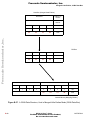
Reset Configuration Write Through the DSI, Timing Diagram. . . . . . . . . . . . . . . . . . . . . 2-6
Configuring Multiple MSC8102 Devices From the DSI Port . . . . . . . . . . . . . . . . . . . . . . 2-7
Configuring a Single MSC8102 from the DSI Port . . . . . . . . . . . . . . . . . . . . . . . . . . . . . . 2-8
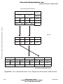
Reset Configuration Write Through the System Bus . . . . . . . . . . . . . . . . . . . . . . . . . . . . . 2-9
Configuring a Single MSC8102 Device With Default Configuration . . . . . . . . . . . . . . . 2-10
Configuring a Single MSC8102 Device From EPROM. . . . . . . . . . . . . . . . . . . . . . . . . . 2-10
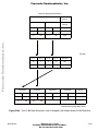
Configuration Master MSC8102 With a Single MSC8102 Slave . . . . . . . . . . . . . . . . . . 2-11
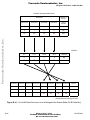
Configuring Multiple MSC8102 Devices. . . . . . . . . . . . . . . . . . . . . . . . . . . . . . . . . . . . . 2-13
TDM Boot System . . . . . . . . . . . . . . . . . . . . . . . . . . . . . . . . . . . . . . . . . . . . . . . . . . . . . . 2-18
Receive Frame Non-T1 Configuration . . . . . . . . . . . . . . . . . . . . . . . . . . . . . . . . . . . . . . . 2-19
16 bit receive Frame Non-T1 Configuration . . . . . . . . . . . . . . . . . . . . . . . . . . . . . . . . . . 2-19
Receive Frame T1 Configuration . . . . . . . . . . . . . . . . . . . . . . . . . . . . . . . . . . . . . . . . . . . 2-20
Transmit Frame Non-T1 Configuration . . . . . . . . . . . . . . . . . . . . . . . . . . . . . . . . . . . . . . 2-20
Transmit Frame T1 Configuration . . . . . . . . . . . . . . . . . . . . . . . . . . . . . . . . . . . . . . . . . . 2-21
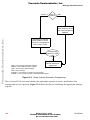
MSC8102 Logic Layer Algorithm . . . . . . . . . . . . . . . . . . . . . . . . . . . . . . . . . . . . . . . . . . 2-24
TDM Block Stream Structure Example From TDM Master Boot Device . . . . . . . . . . . . 2-25
UART Boot System . . . . . . . . . . . . . . . . . . . . . . . . . . . . . . . . . . . . . . . . . . . . . . . . . . . . . 2-26
CORES_CLOCK and BUSES_CLOCK Generation . . . . . . . . . . . . . . . . . . . . . . . . . . . . 2-28
CORE_CLOCKS, BUSES_CLOCK, and CLKOUT Example . . . . . . . . . . . . . . . . . . . . 2-28
MSC8102 Clock Distribution And Synchronization In DLL Enable Mode . . . . . . . . . . 2-29
MSC8102 Clock Distribution And Synchronization In DLL Disable Mode . . . . . . . . . . 2-30
MSC8102 Internal Memory Organization . . . . . . . . . . . . . . . . . . . . . . . . . . . . . . . . . . . . . 3-2
M1–M2 Code/Data Split. . . . . . . . . . . . . . . . . . . . . . . . . . . . . . . . . . . . . . . . . . . . . . . . . . . 3-5
MSC8102 User’s Guide
For More Information On This Product,
Go to: www.freescale.com
xi
Freescale Semiconductor, Inc.
Freescale Semiconductor, Inc...
Figures
Figure 3-3.
Figure 3-4.
Figure 4-1.
Figure 4-2.
Figure 4-3.
Figure 4-4.
Figure 4-5.
Figure 4-6.
Figure 4-7.
Figure 4-8.
Figure 4-9.
Figure 4-10.
Figure 5-1.
Figure 5-2.
Figure 5-3.
Figure 5-4.
Figure 5-5.
Figure 5-6.
Figure 6-1.
Figure 6-2.
Figure 6-3.
Figure 6-4.
Figure 6-5.
Figure 6-6.
Figure 6-7.
Figure 6-8.
Figure 6-9.
Figure 6-10.
Figure 7-1.
Figure 7-2.
Figure 7-3.
Figure 7-4.
Figure 7-5.
Figure 7-6.
Figure 7-7.
Figure 7-8.
Figure 8-1.
Figure 8-2.
xii
Relative Code/Data Weighting . . . . . . . . . . . . . . . . . . . . . . . . . . . . . . . . . . . . . . . . . . . . . . 3-6
Cache Multitasking Support . . . . . . . . . . . . . . . . . . . . . . . . . . . . . . . . . . . . . . . . . . . . . . . . 3-7
Memory Controller Machine Selection . . . . . . . . . . . . . . . . . . . . . . . . . . . . . . . . . . . . . . . 4-3
MSC8102 to Flash Interconnect in Single-Master Bus Mode . . . . . . . . . . . . . . . . . . . . . . 4-5
Flash Memory Read, Single-Master Bus Mode . . . . . . . . . . . . . . . . . . . . . . . . . . . . . . . . . 4-6
Flash Memory Write, Single-Master Bus Mode. . . . . . . . . . . . . . . . . . . . . . . . . . . . . . . . . 4-7
MSC8102 to SDRAM Interconnect in Single-Master Bus Mode . . . . . . . . . . . . . . . . . . . 4-8
MSC8102 SDRAM Address Multiplexing. . . . . . . . . . . . . . . . . . . . . . . . . . . . . . . . . . . . . 4-9
SDRAM Burst Read Page Miss, Single-Master Bus Mode . . . . . . . . . . . . . . . . . . . . . . . 4-11
SDRAM Burst Write Page Miss, Single-Master Bus Mode. . . . . . . . . . . . . . . . . . . . . . . 4-12
SDRAM Mode Register Programming. . . . . . . . . . . . . . . . . . . . . . . . . . . . . . . . . . . . . . . 4-14
MSC8102 to SDRAM Interconnect in Multi-Master Bus Mode . . . . . . . . . . . . . . . . . . . 4-15
MSC8102 Interrupt Block Diagram . . . . . . . . . . . . . . . . . . . . . . . . . . . . . . . . . . . . . . . . . . 5-2
PIC Block Diagram. . . . . . . . . . . . . . . . . . . . . . . . . . . . . . . . . . . . . . . . . . . . . . . . . . . . . . . 5-3
LIC Block Diagram . . . . . . . . . . . . . . . . . . . . . . . . . . . . . . . . . . . . . . . . . . . . . . . . . . . . . . 5-8
LIC Group B Interrupt Configuration Register 1 . . . . . . . . . . . . . . . . . . . . . . . . . . . . . . . 5-11
LIC Group B Interrupt Enable Register . . . . . . . . . . . . . . . . . . . . . . . . . . . . . . . . . . . . . . 5-11
GIC Connectivity . . . . . . . . . . . . . . . . . . . . . . . . . . . . . . . . . . . . . . . . . . . . . . . . . . . . . . . 5-12
MSC8102 Bus Structure . . . . . . . . . . . . . . . . . . . . . . . . . . . . . . . . . . . . . . . . . . . . . . . . . . . 6-1
Extended Core Block Diagram . . . . . . . . . . . . . . . . . . . . . . . . . . . . . . . . . . . . . . . . . . . . . . 6-2
MQBus Interaction . . . . . . . . . . . . . . . . . . . . . . . . . . . . . . . . . . . . . . . . . . . . . . . . . . . . . . . 6-3
SQBus interaction . . . . . . . . . . . . . . . . . . . . . . . . . . . . . . . . . . . . . . . . . . . . . . . . . . . . . . . . 6-4
SQBus interaction . . . . . . . . . . . . . . . . . . . . . . . . . . . . . . . . . . . . . . . . . . . . . . . . . . . . . . . . 6-4
Local Bus Interaction . . . . . . . . . . . . . . . . . . . . . . . . . . . . . . . . . . . . . . . . . . . . . . . . . . . . . 6-5
System Bus External Memory Access Example. . . . . . . . . . . . . . . . . . . . . . . . . . . . . . . . . 6-6
Example Memory Map . . . . . . . . . . . . . . . . . . . . . . . . . . . . . . . . . . . . . . . . . . . . . . . . . . . . 6-7
SIU Block Diagram . . . . . . . . . . . . . . . . . . . . . . . . . . . . . . . . . . . . . . . . . . . . . . . . . . . . . . 6-9
Bus Architecture . . . . . . . . . . . . . . . . . . . . . . . . . . . . . . . . . . . . . . . . . . . . . . . . . . . . . . . . 6-10
DMA System . . . . . . . . . . . . . . . . . . . . . . . . . . . . . . . . . . . . . . . . . . . . . . . . . . . . . . . . . . . 7-2
DMA Buffer Types. . . . . . . . . . . . . . . . . . . . . . . . . . . . . . . . . . . . . . . . . . . . . . . . . . . . . . . 7-8
DMA Interrupt Scheme . . . . . . . . . . . . . . . . . . . . . . . . . . . . . . . . . . . . . . . . . . . . . . . . . . . 7-9
Burst Transaction from External Memory to M1 Memory of SC140 Core 0 . . . . . . . . . 7-16
M1 Memory Zero Stuffing . . . . . . . . . . . . . . . . . . . . . . . . . . . . . . . . . . . . . . . . . . . . . . . . 7-19
Double M1 Flyby Transactions . . . . . . . . . . . . . . . . . . . . . . . . . . . . . . . . . . . . . . . . . . . . 7-20
DMA Message System . . . . . . . . . . . . . . . . . . . . . . . . . . . . . . . . . . . . . . . . . . . . . . . . . . . 7-22
DREQ2 Burst Transfer Control . . . . . . . . . . . . . . . . . . . . . . . . . . . . . . . . . . . . . . . . . . . . 7-24
MSC8101 Host to MSC8102 DSI Hardware interface. . . . . . . . . . . . . . . . . . . . . . . . . . . . 8-5
Asynchronous DSI UPM Read Cycle, 100 MHz . . . . . . . . . . . . . . . . . . . . . . . . . . . . . . . . 8-8
MSC8102 User’s Guide
For More Information On This Product,
Go to: www.freescale.com
MOTOROLA
Freescale Semiconductor, Inc...
Freescale Semiconductor, Inc.
Figure 8-3.
Figure 9-1.
Figure 9-2.
Figure 9-3.
Figure 9-4.
Figure 9-5.
Figure 9-6.
Figure 9-7.
Figure 9-8.
Figure 9-9.
Figure 10-1.
Figure 10-2.
Figure 10-3.
Figure 10-4.
Figure 10-5.
Figure 10-6.
Figure 10-7.
Figure 10-8.
Figure 10-9.
Figure 10-10.
Figure 10-11.
Figure 10-12.
Figure 10-13.
Figure 11-1.
Figure 12-1.
Figure 12-2.
Figure 12-3.
Figure 12-4.
Figure 12-5.
Figure B-1.
Figure B-2.
Figure B-3.
Figure B-4.
Figure B-5.
Figure B-7.
Figure B-8.
Figure B-9.
Figure B-10.
MOTOROLA
Asynchronous DSI UPM Write Cycle, 100 MHz. . . . . . . . . . . . . . . . . . . . . . . . . . . . . . . . 8-9
Pin Configuration When TDM Does Not Share Signals with Other TDMs . . . . . . . . . . . 9-4
Pin Configuration When A TDM Shares Signals with Other TDMs . . . . . . . . . . . . . . . . . 9-5
Pin Configuration When A TDM Shares Signals with Other TDMs cont. . . . . . . . . . . . . 9-6
TDM0 Receive and Transmit Interface . . . . . . . . . . . . . . . . . . . . . . . . . . . . . . . . . . . . . . . 9-8
Receive Threshold Operation . . . . . . . . . . . . . . . . . . . . . . . . . . . . . . . . . . . . . . . . . . . . . . 9-11
Data Buffer Location . . . . . . . . . . . . . . . . . . . . . . . . . . . . . . . . . . . . . . . . . . . . . . . . . . . . 9-13
TDM0 Local Memory. . . . . . . . . . . . . . . . . . . . . . . . . . . . . . . . . . . . . . . . . . . . . . . . . . . . 9-17
Received Data After First Threshold Interrupt . . . . . . . . . . . . . . . . . . . . . . . . . . . . . . . . . 9-20
Received Data After Second Threshold Interrupt. . . . . . . . . . . . . . . . . . . . . . . . . . . . . . . 9-21
JTAG and EOnCE Multi-core Interconnection . . . . . . . . . . . . . . . . . . . . . . . . . . . . . . . . 10-2
TAP Controller State Machine . . . . . . . . . . . . . . . . . . . . . . . . . . . . . . . . . . . . . . . . . . . . . 10-4
Cascading Multiple EOnCE Modules. . . . . . . . . . . . . . . . . . . . . . . . . . . . . . . . . . . . . . . . 10-6
Reading and Writing EOnCE Registers Via JTAG . . . . . . . . . . . . . . . . . . . . . . . . . . . . . 10-7
Selected SC140 Core Issues a Debug Request to All Other SC140 Cores. . . . . . . . . . . . 10-8
Board EE Pin Interconnectivity . . . . . . . . . . . . . . . . . . . . . . . . . . . . . . . . . . . . . . . . . . . . 10-9
CORE_CMD Instruction Format . . . . . . . . . . . . . . . . . . . . . . . . . . . . . . . . . . . . . . . . . . 10-13
Executing DEBUG_REQUEST . . . . . . . . . . . . . . . . . . . . . . . . . . . . . . . . . . . . . . . . . . . 10-16
Reading MSC8102 IDCODE . . . . . . . . . . . . . . . . . . . . . . . . . . . . . . . . . . . . . . . . . . . . . 10-17
Writing to EOnCE Registers. . . . . . . . . . . . . . . . . . . . . . . . . . . . . . . . . . . . . . . . . . . . . . 10-18
Reading EOnCE Registers . . . . . . . . . . . . . . . . . . . . . . . . . . . . . . . . . . . . . . . . . . . . . . . 10-19
Executing a Single Instruction . . . . . . . . . . . . . . . . . . . . . . . . . . . . . . . . . . . . . . . . . . . . 10-20
Reading From ETRSMT. . . . . . . . . . . . . . . . . . . . . . . . . . . . . . . . . . . . . . . . . . . . . . . . . 10-22
Cascaded Timers. . . . . . . . . . . . . . . . . . . . . . . . . . . . . . . . . . . . . . . . . . . . . . . . . . . . . . . . 11-2
Semaphore Locking and Unlocking . . . . . . . . . . . . . . . . . . . . . . . . . . . . . . . . . . . . . . . . . 12-2
Multi-Master Access to Shared Resource. . . . . . . . . . . . . . . . . . . . . . . . . . . . . . . . . . . . . 12-3
Virtual Interrupt Generation Programming . . . . . . . . . . . . . . . . . . . . . . . . . . . . . . . . . . . 12-4
Receiving Virtual Interrupt Initialization . . . . . . . . . . . . . . . . . . . . . . . . . . . . . . . . . . . . . 12-5
Virtual Interrupt Servicing . . . . . . . . . . . . . . . . . . . . . . . . . . . . . . . . . . . . . . . . . . . . . . . . 12-6
DSI Bus to Host in Big Endian Mode (64-Bit Data Bus) . . . . . . . . . . . . . . . . . . . . . . . . . B-2
One 64-Bit Data Structure, Host in Big Endian Mode (64-Bit Data Bus) . . . . . . . . . . . . B-3
Two 32-Bit Data Structures, Host in Big Endian Mode (64-Bit Data Bus) . . . . . . . . . . . B-4
Four 16-Bit Data Structures, Host in Big Endian Mode (64-Bit Data Bus) . . . . . . . . . . . B-5
Eight 8-Bit Data Structures, Host in Big Endian Mode (64-Bit Data Bus) . . . . . . . . . . . B-6
DSI Bus to Host in Little Endian Mode (64-Bit Data Bus) . . . . . . . . . . . . . . . . . . . . . . . B-8
One 64-Bit Data Structure, Host in Little Endian Mode (64-Bit Data Bus). . . . . . . . . . . B-9
Two 32-Bit Data Structures, Host in Little Endian Mode (64-Bit Data Bus) . . . . . . . . B-10
Four 16-Bit Data Structures, Host in Little Endian Mode (64-Bit Data Bus) . . . . . . . . B-11
MSC8102 User’s Guide
For More Information On This Product,
Go to: www.freescale.com
xiii
Freescale Semiconductor, Inc.
Freescale Semiconductor, Inc...
Figures
Figure B-11.
Figure B-12.
Figure B-14.
Figure B-15.
Figure B-16.
Figure B-17.
Figure B-18.
Figure B-20.
Figure B-21.
Figure B-22.
Figure B-23.
Figure B-24.
Figure B-25.
Figure B-26.
Figure B-28.
Figure B-29.
Figure B-30.
Figure B-31.
Figure B-32.
Figure B-33.
Figure B-34.
Figure B-36.
Figure B-37.
Figure B-38.
Figure B-39.
Figure B-40.
Figure B-41.
Figure B-42.
Figure C-1.
Figure C-2.
Figure D-1.
Figure D-2.
xiv
One 16-Bit Data Structure, Host in Little Endian Mode (64-Bit Data Bus). . . . . . . . . . B-12
Eight 8-Bit Data Structures, Host in Little Endian Mode (64-Bit Data Bus) . . . . . . . . . B-13
DSI Bus to Host in Munged Little Endian Mode (64-Bit Data Bus) . . . . . . . . . . . . . . . B-15
A 64-Bit Data Structure, Host in Munged Little Endian Mode (64-Bit Data Bus) . . . . B-16
Two 32-Bit Data Structures, Host in Munged Little Endian Mode (64-Bit Data Bus) . B-17
Four 16-Bit Data Structures, Host in Munged Little Endian Mode (64-Bit Data Bus) . B-18
Eight 8-Bit Data Structures, Host in Munged Little Endian Mode (64-Bit Data Bus). . B-19
DSI Bus to Host in Big Endian Mode (32-Bit Data Bus) . . . . . . . . . . . . . . . . . . . . . . . . B-21
One 32-Bit Data Structure, Host in Big Endian Mode (32-Bit Data Bus) . . . . . . . . . . . B-22
One 32-Bit Data Structure, Host in Big Endian Mode (32-Bit Data Bus) . . . . . . . . . . . B-23
Two 16-Bit Data Structures, Host in Big Endian Mode (32-Bit Data Bus) . . . . . . . . . . B-24
Two 16-Bit Data Structures, Host in Big Endian Mode (32-Bit Data Bus) . . . . . . . . . . B-25
Four 8-Bit Data Structures, Host in Big Endian Mode (32-Bit Data Bus) . . . . . . . . . . . B-26
Four 8-Bit Data Structures, Host in Big Endian Mode (32-Bit Data Bus) . . . . . . . . . . . B-27
DSI Bus to Host in Little Endian Mode (32-Bit Data Bus) . . . . . . . . . . . . . . . . . . . . . . B-29
One 32-Bit Data Structure, Host in Little Endian Mode (32-Bit Data Bus). . . . . . . . . . B-30
One 32-Bit Data Structure, Host in Little Endian Mode (32-Bit Data Bus). . . . . . . . . . B-31
Two 16-Bit Data Structures, Host in Little Endian Mode (32-Bit Data Bus) . . . . . . . . B-32
Two 16-Bit Data Structures, Host in Little Endian Mode (32-Bit Data Bus) . . . . . . . . B-33
Four 8-Bit Data Structures, Host in Little Endian Mode (32-Bit Data Bus) . . . . . . . . . B-34
Four 8-Bit Data Structures, Host in Little Endian Mode (32-Bit Data Bus) . . . . . . . . . B-35
DSI Bus to Host in Munged Little Endian Mode (32-Bit Data Bus) . . . . . . . . . . . . . . . B-37
A 32-Bit Data Structure, Host in Munged Little Endian Mode (32-Bit Data Bus) . . . . B-38
A 32-Bit Data Structure, Host in Munged Little Endian Mode (32-Bit Data Bus) . . . . B-39
Two 16-Bit Data Structures, Host in Munged Little Endian Mode (32-Bit Data Bus) . B-40
Two 16-Bit Data Structures, Host in Munged Little Endian Mode (32-Bit Data Bus) . B-41
Four 8-Bit Data Structures, Host in Munged Little Endian Mode (32-Bit Data Bus) . . B-42
Four 8-Bit Data Structure, Host in Munged Little Endian Mode (32-Bit Data Bus) . . . B-43
Connecting an MSC8101 Device to Multiple MSC8102 Devices . . . . . . . . . . . . . . . . . . C-1
Connecting an MPC8260 Device to Multiple MSC8102 Devices . . . . . . . . . . . . . . . . . . C-2
Accessing the Internal Memory Map in Sliding Window Addressing Mode. . . . . . . . . . D-1
Address Flow for a DSI Access in Sliding Window Addressing Mode. . . . . . . . . . . . . . D-2
MSC8102 User’s Guide
For More Information On This Product,
Go to: www.freescale.com
MOTOROLA
Freescale Semiconductor, Inc.
Freescale Semiconductor, Inc...
Tables
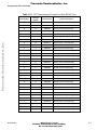
Table 1-1.
Table 1-2.
Table 1-3.
Table 1-4.
Table 1-5.
Table 1-6.
Table 1-7.
Table 1-8.
Table 1-9.
Table 1-10.
Table 2-1.
Table 2-2.
Table 2-3.
Table 2-4.
Table 2-5.
Table 2-6.
Table 2-7.
Table 2-8.
Table 2-9.
Table 2-10.
Table 2-11.
Table 2-12.
Table 4-1.
Table 4-2.
Table 4-3.
Table 5-1.
Table 5-2.
Table 5-3.
Table 5-4.
Table 5-5.
Table 5-6.
Table 5-7.
Table 5-8.
Table 6-1.
MOTOROLA
Extended SC140 Cores and Core Memories . . . . . . . . . . . . . . . . . . . . . . . . . . . . . . . . . . . . . 1-2
Phase-Lock Loop (PLL) . . . . . . . . . . . . . . . . . . . . . . . . . . . . . . . . . . . . . . . . . . . . . . . . . . . . 1-2
Memory Controller and Buses . . . . . . . . . . . . . . . . . . . . . . . . . . . . . . . . . . . . . . . . . . . . . . . . 1-3
DMA Controller . . . . . . . . . . . . . . . . . . . . . . . . . . . . . . . . . . . . . . . . . . . . . . . . . . . . . . . . . . . 1-4
Serial Interfaces . . . . . . . . . . . . . . . . . . . . . . . . . . . . . . . . . . . . . . . . . . . . . . . . . . . . . . . . . . . 1-4
Miscellaneous Modules . . . . . . . . . . . . . . . . . . . . . . . . . . . . . . . . . . . . . . . . . . . . . . . . . . . . . 1-5
Power and Packaging . . . . . . . . . . . . . . . . . . . . . . . . . . . . . . . . . . . . . . . . . . . . . . . . . . . . . . . 1-6
Software Support . . . . . . . . . . . . . . . . . . . . . . . . . . . . . . . . . . . . . . . . . . . . . . . . . . . . . . . . . . 1-6
Application Development System (ADS) Board . . . . . . . . . . . . . . . . . . . . . . . . . . . . . . . . . . 1-7
DMA Transfers . . . . . . . . . . . . . . . . . . . . . . . . . . . . . . . . . . . . . . . . . . . . . . . . . . . . . . . . . . 1-17
Reset Sources . . . . . . . . . . . . . . . . . . . . . . . . . . . . . . . . . . . . . . . . . . . . . . . . . . . . . . . . . . . . . 2-1
Reset Actions for Each Reset Source . . . . . . . . . . . . . . . . . . . . . . . . . . . . . . . . . . . . . . . . . . 2-2
External Configuration Signals . . . . . . . . . . . . . . . . . . . . . . . . . . . . . . . . . . . . . . . . . . . . . . . 2-3
Reset Configuration Modes . . . . . . . . . . . . . . . . . . . . . . . . . . . . . . . . . . . . . . . . . . . . . . . . . . 2-5
RSTCONF Connections in Multi-MSC8102 Systems . . . . . . . . . . . . . . . . . . . . . . . . . . . . . 2-12
Configuration EPROM Addresses . . . . . . . . . . . . . . . . . . . . . . . . . . . . . . . . . . . . . . . . . . . . 2-12
Boot Mode Operation . . . . . . . . . . . . . . . . . . . . . . . . . . . . . . . . . . . . . . . . . . . . . . . . . . . . . 2-14
Default MSC8102 Initialization Values of the Boot Program . . . . . . . . . . . . . . . . . . . . . . . 2-15
External Memory Address Table (32-Bit Wide EPROM) . . . . . . . . . . . . . . . . . . . . . . . . . . 2-17
Block Transfer Message . . . . . . . . . . . . . . . . . . . . . . . . . . . . . . . . . . . . . . . . . . . . . . . . . . . 2-21
Block Transfer Acknowledge Message . . . . . . . . . . . . . . . . . . . . . . . . . . . . . . . . . . . . . . . . 2-22
SCMR Bit Descriptions . . . . . . . . . . . . . . . . . . . . . . . . . . . . . . . . . . . . . . . . . . . . . . . . . . . . 2-31
GPCM Option Register Settings . . . . . . . . . . . . . . . . . . . . . . . . . . . . . . . . . . . . . . . . . . . . . . 4-6
SDRAM Controller Settings . . . . . . . . . . . . . . . . . . . . . . . . . . . . . . . . . . . . . . . . . . . . . . . . 4-10
SDRAM Timing Control Values . . . . . . . . . . . . . . . . . . . . . . . . . . . . . . . . . . . . . . . . . . . . . 4-11
PIC Edge/Level-Triggered Interrupt Priority Registers . . . . . . . . . . . . . . . . . . . . . . . . . . . . . 5-3
Interrupt Priority Levels . . . . . . . . . . . . . . . . . . . . . . . . . . . . . . . . . . . . . . . . . . . . . . . . . . . . . 5-4
PIC Interrupt Pending Registers . . . . . . . . . . . . . . . . . . . . . . . . . . . . . . . . . . . . . . . . . . . . . . 5-4
MSC8102 Interrupt Routing . . . . . . . . . . . . . . . . . . . . . . . . . . . . . . . . . . . . . . . . . . . . . . . . . 5-5
LIC Group A Registers . . . . . . . . . . . . . . . . . . . . . . . . . . . . . . . . . . . . . . . . . . . . . . . . . . . . . 5-9
LIC Group B Registers . . . . . . . . . . . . . . . . . . . . . . . . . . . . . . . . . . . . . . . . . . . . . . . . . . . . . 5-9
LIC Interrupt Group A Sources (Same for all SC140 Cores) . . . . . . . . . . . . . . . . . . . . . . . . 5-9
LIC Interrupt Group B Source for SC140 Cores 0–3 . . . . . . . . . . . . . . . . . . . . . . . . . . . . . 5-10
Features of the System Bus and Local Bus . . . . . . . . . . . . . . . . . . . . . . . . . . . . . . . . . . . . . . 6-6
MSC8102 User’s Guide
For More Information On This Product,
Go to: www.freescale.com
xv
Freescale Semiconductor, Inc.
Freescale Semiconductor, Inc...
Tables
Table 7-1.
Table 7-2.
Table 7-3.
Table 8-1.
Table 8-2.
Table 8-3.
Table 8-4.
Table 8-5.
Table 8-6.
Table 8-7.
Table 8-8.
Table 8-9.
Table 9-1.
Table 9-2.
Table 9-3.
Table 9-4.
Table 9-5.
Table 9-6.
Table 9-7.
Table 9-8.
Table 9-9.
Table 9-10.
Table 9-11.
Table 9-12.
Table 9-13.
Table 9-14.
Table 9-15.
Table 10-1.
Table 10-2.
Table 10-3.
Table 10-4.
Table 10-5.
Table 10-6.
Table 10-7.
Table 10-8.
Table 11-1.
Table 11-2.
Table D-1.
Table D-2.
xvi
DMA Registers . . . . . . . . . . . . . . . . . . . . . . . . . . . . . . . . . . . . . . . . . . . . . . . . . . . . . . . . . . 7-10
DCPRAM Addressing . . . . . . . . . . . . . . . . . . . . . . . . . . . . . . . . . . . . . . . . . . . . . . . . . . . . . 7-12
Buffer Descriptor Parameters . . . . . . . . . . . . . . . . . . . . . . . . . . . . . . . . . . . . . . . . . . . . . . . 7-13
Full Address Mode Decoding DCR[0]:SLDWA] = 0 . . . . . . . . . . . . . . . . . . . . . . . . . . . . . . 8-1
Sliding Window Address Mode Decoding DCR[0]:SLDWA] = 1 . . . . . . . . . . . . . . . . . . . . 8-2
MSC8102 Internal Memory Space Viewed Through DSI . . . . . . . . . . . . . . . . . . . . . . . . . . . 8-2
DSI Endian Mode Selection . . . . . . . . . . . . . . . . . . . . . . . . . . . . . . . . . . . . . . . . . . . . . . . . . 8-4
Slave Hardware Pin Configuration . . . . . . . . . . . . . . . . . . . . . . . . . . . . . . . . . . . . . . . . . . . . 8-6
Asynchronous DSI UPMA Settings . . . . . . . . . . . . . . . . . . . . . . . . . . . . . . . . . . . . . . . . . . 8-10
Host MSC8101 Memory Controller Register Settings . . . . . . . . . . . . . . . . . . . . . . . . . . . . 8-10
Slave MSC8102 Register Settings . . . . . . . . . . . . . . . . . . . . . . . . . . . . . . . . . . . . . . . . . . . . 8-11
Slave MSC8102 UPMC Settings . . . . . . . . . . . . . . . . . . . . . . . . . . . . . . . . . . . . . . . . . . . . . 8-12
TDM Signal Pins . . . . . . . . . . . . . . . . . . . . . . . . . . . . . . . . . . . . . . . . . . . . . . . . . . . . . . . . . . 9-1
General Interface Bit Settings . . . . . . . . . . . . . . . . . . . . . . . . . . . . . . . . . . . . . . . . . . . . . . . . 9-6
Receive Bit Settings . . . . . . . . . . . . . . . . . . . . . . . . . . . . . . . . . . . . . . . . . . . . . . . . . . . . . . . . 9-6
Transmit Bit Settings . . . . . . . . . . . . . . . . . . . . . . . . . . . . . . . . . . . . . . . . . . . . . . . . . . . . . . . 9-7
TDM0RFP Bit Settings . . . . . . . . . . . . . . . . . . . . . . . . . . . . . . . . . . . . . . . . . . . . . . . . . . . . . 9-8
TDM0TFP Bit Settings . . . . . . . . . . . . . . . . . . . . . . . . . . . . . . . . . . . . . . . . . . . . . . . . . . . . . 9-8
Buffer Size Bit Settings . . . . . . . . . . . . . . . . . . . . . . . . . . . . . . . . . . . . . . . . . . . . . . . . . . . . . 9-9
Global Data Buffer Bit Settings . . . . . . . . . . . . . . . . . . . . . . . . . . . . . . . . . . . . . . . . . . . . . . . 9-9
Threshold Pointer Bit Settings . . . . . . . . . . . . . . . . . . . . . . . . . . . . . . . . . . . . . . . . . . . . . . . 9-11
Threshold Interrupt Bit Settings . . . . . . . . . . . . . . . . . . . . . . . . . . . . . . . . . . . . . . . . . . . . . 9-12
Threshold Interrupts . . . . . . . . . . . . . . . . . . . . . . . . . . . . . . . . . . . . . . . . . . . . . . . . . . . . . . . 9-12
Channel Buffer Location . . . . . . . . . . . . . . . . . . . . . . . . . . . . . . . . . . . . . . . . . . . . . . . . . . . 9-13
Channel Parameter Bit Settings . . . . . . . . . . . . . . . . . . . . . . . . . . . . . . . . . . . . . . . . . . . . . . 9-14
Calculation of Channel Address in TDM Local Memory . . . . . . . . . . . . . . . . . . . . . . . . . . 9-16
Bit Settings to Enable the TDM . . . . . . . . . . . . . . . . . . . . . . . . . . . . . . . . . . . . . . . . . . . . . . 9-18
JTAG Instructions . . . . . . . . . . . . . . . . . . . . . . . . . . . . . . . . . . . . . . . . . . . . . . . . . . . . . . . . 10-3
JTAG Scan Paths . . . . . . . . . . . . . . . . . . . . . . . . . . . . . . . . . . . . . . . . . . . . . . . . . . . . . . . . . 10-4
Instruction Register Capture and SC140 Core Status Values . . . . . . . . . . . . . . . . . . . . . . . 10-8
EOnCE Control Register (ECR) Bits . . . . . . . . . . . . . . . . . . . . . . . . . . . . . . . . . . . . . . . . . . 10-9
EOnCE Register Summary . . . . . . . . . . . . . . . . . . . . . . . . . . . . . . . . . . . . . . . . . . . . . . . . 10-10
CORE_CMD Word Lengths . . . . . . . . . . . . . . . . . . . . . . . . . . . . . . . . . . . . . . . . . . . . . . . 10-12
Trace Buffer Register Set . . . . . . . . . . . . . . . . . . . . . . . . . . . . . . . . . . . . . . . . . . . . . . . . . 10-25
Event Register Sets . . . . . . . . . . . . . . . . . . . . . . . . . . . . . . . . . . . . . . . . . . . . . . . . . . . . . . 10-26
Output Frequency As A Function Of Input Frequency . . . . . . . . . . . . . . . . . . . . . . . . . . . . 11-6
LIC Timer Interrupt Sources For Each SC140 Core . . . . . . . . . . . . . . . . . . . . . . . . . . . . . . 11-7
Full Bus Addressing Mode . . . . . . . . . . . . . . . . . . . . . . . . . . . . . . . . . . . . . . . . . . . . . . . . . . D-3
Sliding Window Addressing Mode . . . . . . . . . . . . . . . . . . . . . . . . . . . . . . . . . . . . . . . . . . . . D-3
MSC8102 User’s Guide
For More Information On This Product,
Go to: www.freescale.com
MOTOROLA
Freescale Semiconductor, Inc.
Freescale Semiconductor, Inc...
About This
Book
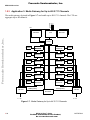
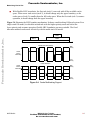
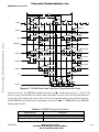
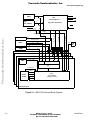
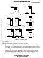
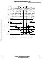
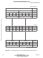
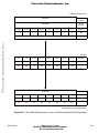
The MSC8102 device is based on the SC140 DSP core introduced by the StarCore® Alliance. It
addresses the challenges of the networking market. The benefits of the MSC8102 include not only a
very high level of performance but also a product design that enables effective software development
and integration. Its tool suite provides a full-featured development environment for C/C++ and
assembly languages as well as ease of integration with third-party software, such as off-the-shelf
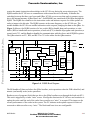
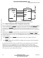
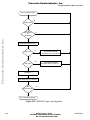
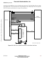
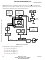
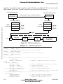
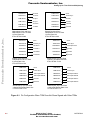
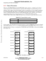
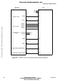
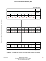
libraries and a real-time operating system. The MSC8102 device is logically partitioned into three
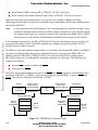
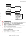
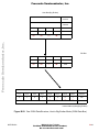
distinct blocks: an extended core, a system interface unit (SIU), and communications peripherals:
Serial I/O
Communications
Peripherals
SIU
Four Extended Cores
System Bus
Direct Slave Interface
Four Extended Cores
SIU
Each contains an SC140 core with internal memory for data
and program storage, peripheral hardware, and two interrupt
controllers. Memory includes 224 KB (896 KB total) of zero
wait state SRAM and 16 KB (64 KB total) of instruction cache.
The MSC8102 also includes 476 KB of shared memory (M2)
and 4 KB of boot ROM. Minimum code density is achieved
using a 16-bit instruction set that is grouped into execution
sets by the compiler (or by the programmer) for high
instruction parallelism.The direct slave interface (DSI)
provides a glueless 32/64-bit interface to a host processor for
data and command communication. The programmable
interrupt controller (PIC) and local interrupt controller (LIC)
process all internal interrupt requests, notifying the SC140
cores or external devices of an interrupt event.
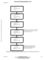
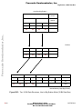
Supports internal and
external system-related
functions. The SIU
includes hardware such
as a direct memory
access (DMA)
controller, clocks, and
reset configuration
registers. It also
includes the memory
controllers, which
interface to external
memory devices and/or
other devices such as a
system host or other
DSPs.
MOTOROLA
MSC8102 User’s Guide
For More Information On This Product,
Go to: www.freescale.com
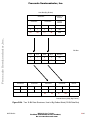
Communication
Peripherals
Includes four TDM
interfaces supporting
256 channels each, a
UART, thirty-two 16-bit
timers, thirty-two
programmable GPIO
signals, eight hardware
semaphore registers,
and a global interrupt
controller (GIC). The
serial interfaces give
additional functionality
and flexibility. The
semaphore registers
provide resource control
for external hosts. The
GIC extends interrupt
handling capability.
xvii
Freescale Semiconductor, Inc.
About This Book
Before Using This Manual—Important Note
This manual explains how to program various features of the MSC8102 device. The information in
this manual is subject to change without notice, as described in the disclaimers on the title page of this
manual. Before using this manual, determine whether it is the latest revision and whether there are
errata or addenda. To locate any published errata or updates associated with this manual or this
product, refer to the world-wide web site listed on the back cover of this manual or call your local
distributor or sales representative.
Freescale Semiconductor, Inc...
Audience and Helpful Hints
This manual is for software and hardware developers and applications programmers who are
developing products using the MSC8102 device. It assumes that you have a working knowledge of
DSP technology. This user’s guide begins with a system overview and then covers specific
programming topics. For your convenience, the chapters of this manual are organized to make the
information flow as predictable as possible. Most chapters begin with a quick review of basics for the
topic MSC8102 module(s) and then present programming procedures, typically illustrated with
examples. Most chapters end with a “Related Reading” section that summarizes other relevant parts
of the StarCore and MSC8102 documentation.
Notational Conventions and Definitions
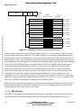
This manual uses the following notational conventions:
xviii
mnemonics
Instruction mnemonics appear in lowercase bold.
COMMAND NAMES
Command names are set in small caps, as follows: GRACEFUL STOP TRANSMIT or ENTER HUNT
MODE.
italics
Book titles in text are set in italics. Also, italics are used for emphasis and to highlight the main
items in bulleted lists.
0x
Prefix to denote a hexadecimal number.
0b
Prefix to denote a binary number.
REG[#]:FIELD
Abbreviations or acronyms for registers or buffer descriptors appear in uppercase text.
Following the register name is the bit number or field number range in brackets, and then the
bit or field name. For example, ICR[8]:INIT refers to the Force Initialization bit (bit 8) in the host
Interface Control Register.
Active high
signals
Names of active high signals appear in small caps, sans serif, as follows: TT[0–4], TSIZ[0–3],
and DP[0–7].
Active low
signals
Signal names of active low signals appear in small capital letters in a sans serif typeface, with an
overbar: DBG, AACK, and EXT_BG[2].
x
A lowercase italicized x in a register or signal name indicates that there are multiple registers or
signals with this name. For example, BRCGx refers to BRCG[1–8], and MxMR refers to the
MAMR/MBMR/MCMR registers.
MSC8102 User’s Guide
For More Information On This Product,
Go to: www.freescale.com
MOTOROLA
Freescale Semiconductor, Inc.
Organization
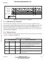
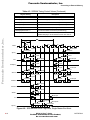
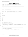
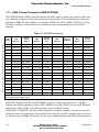
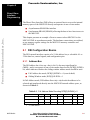
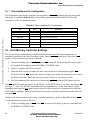
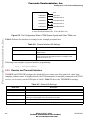
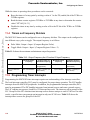
On the MSC8102, the SC140 cores are 16-bit DSP processors. The following table shows the SC140
assembly language data types. See the StarCore SC140 DSP Core Reference Manual
(MNSC140CORE/D) for details.
Freescale Semiconductor, Inc...
SC140 Core Assembly Data Types
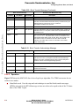
Name
SC140
Byte/Octet
8 bits
Half Word
8 bits
Word
16 bits
Long/Long Word/2 Words
32 bits
Quad Word/4 Words
64 bits
The following table lists the SC140 C language data types recognized by the StarCore C compiler.
See the StarCore SC100 C Compiler User’s Manual (MNSC100CC/D) for details.
SC140 C Language Data Types and Sizes
Name
Size
char/unsigned char
8 bits
short/unsigned short
16 bits
int/unsigned int
16 bits
fractional short
16 bits
long/unsigned long
32 bits
fractional short
32 bits
pointer
32 bits
Organization
Following is a summary and a brief description of the chapters of this manual:
■
Chapter 1, MSC8102 Overview. Features, descriptive overview of main modules,
configurations, and application examples.
■
Chapter 2, Configuring Reset, Boot, and Clock. The MSC8102 reset and boot process and
examples of this process in different system configurations. This chapter concludes with a
discussion of the MSC8102 clocking configuration.
■
Chapter 3, Managing Internal Memory. The memory mechanism of the quad-core MSC8102
and how to allocate the code and data portions efficiently between the internal SC140 M1
memories and the shared M2 memory.
MOTOROLA
MSC8102 User’s Guide
For More Information On This Product,
Go to: www.freescale.com
xix
Freescale Semiconductor, Inc.
Freescale Semiconductor, Inc...
About This Book
■
Chapter 4, Connecting to External Memory. Illustrates several memory interconnection
options for the MSC8102 bus and memory controller. It outlines the hardware connections
and memory register settings for the MSC8102 when the bus is connected to Flash memory,
synchronous DRAM (SDRAM), or an MSC8101 HDI16 slave.
■
Chapter 5, Interrupt Programming. Procedures for handling MSC8102 interrupts. The
chapters focuses on the three MSC8102 interrupt controllers and presents programming
procedures for each.
■
Chapter 6, Managing the Buses. The system bus accesses external memory and any external
60x-compatible bus resources. The local bus provides efficient communication between the
MSC8102 extended cores and the SIU and IPBus peripherals. The MSC8102 has three other
buses outside the extended core: MQBus, SQBus, and IPBus. This chapter describes the
interaction of all of these buses as well as the extended core buses.
■
Chapter 7, Using the DMA Channels. After a discussion of DMA basics, including DMA
configuration, this chapter presents a series of programming examples.
■
Chapter 8, Direct Slave Interface Programming. An example of how to connect a host
MSC8101 to the MSC8102 DSI in asynchronous mode. The hardware connections are
outlined, as are memory register settings for the MSC8101 memory controller and MSC8102
DSI.
■
Chapter 9, Setting Up for Time-Division Multiplexing. The procedure for configuring the
general-purpose I/O (GPIO) pins for TDM operation, programming the TDM configuration
and control registers, initializing the data buffers, and setting up the interrupt routing and
handling.
■
Chapter 10, System-Level Debugging. How the SC140 cores interact with the EOnCE and
JTAG ports (internal debugging modules) after reset and how to configure the daisy-chaining
SC140 cores for efficient system-level debugging. The chapter concludes with a series of
programming examples.
■
Chapter 11, Configuring the Timers. How to program the MSC8102 timers to operate in
various modes and configurations. In addition, example code illustrates the correct procedures
for implementing cascading timers, handling interrupts, and toggling the dedicated output
timer pins.
■
Chapter 12, Managing Shared Resources. How the four SC140 cores on the MSC8102 device
can manage shared resources using hardware semaphores and virtual interrupts
■
Appendixes:
— Appendix A, MSC8102 Dictionary.
— Appendix B, Connecting the DSI in Various Endian Modes
— Appendix C, Connecting Processors to the DSI
— Appendix D, Sliding Window Addressing Guidelines
xx
MSC8102 User’s Guide
For More Information On This Product,
Go to: www.freescale.com
MOTOROLA
Freescale Semiconductor, Inc.
Other MSC8102 Documentation
Freescale Semiconductor, Inc...
Other MSC8102 Documentation
■
MSC8102 Reference Manual. Describes the MSC8101 architecture and functionality in detail,
with a chapter on each of the MSC8101 blocks.
■
MSC8102 Technical Data sheet. Details the signals, AC/DC characteristics, PLL/DLL
performance issues, package and pinout, and electrical design considerations of the MSC8102
device.
■
Application notes. Cover various programming topics related to StarCore and the MSC8102
are available at the Web site listed on the back of this manual.
Further Reading
■
SC140 DSP Core Reference Manual (MNSC140CORE/D), Covers the SC140 core
architecture, instruction set, PLL and clock generator, and EOnCE.
■
Tools-related documentation is as follows:
— SC100 Application Binary Interface Reference Manual.
— SC100 Assembly Language Tools User’s Manual.
— SC100 C/C++ Compiler User’s Manual.
MOTOROLA
MSC8102 User’s Guide
For More Information On This Product,
Go to: www.freescale.com
xxi
Freescale Semiconductor, Inc.
Freescale Semiconductor, Inc...
About This Book
xxii
MSC8102 User’s Guide
For More Information On This Product,
Go to: www.freescale.com
MOTOROLA
Freescale Semiconductor, Inc.
Chapter 1
MSC8102
Overview
1.1 Introduction
Freescale Semiconductor, Inc...
The MSC8102 device is a highly integrated device that combines four StarCore
SC140 cores, four 256-channel Time-Division Multiplexing (TDM) interfaces
with hardware support for µ/A-law decoding/encoding, a UART, a 16-channel
DMA controller, 1436 KB of internal SRAM, 4 KB of boot ROM, a 32/64-bit
Direct Slave Interface (DSI) to support an external host processor, and a flexible
System Interface Unit (SIU). The MSC8102 targets high-bandwidth highly
computational DSP applications and is optimized for wireless transcoding and a
high-density packet telephony DSP farm, as well as high-bandwidth base station
applications. The MSC8102 delivers enhanced performance while maintaining
low power dissipation and greatly reducing system cost.
Each SC140 core has four ALUs and offers 1100 DSP Million Multiply and Add
Commands per Second (MMACS) performance with an internal 275 MHz clock
at 1.6 V. The MSC8102 device delivers a total performance of 4400 DSP
MMACS. Each SC140 core connects to a level-1 224 KB internal memory (M1)
for program and data storage as well as a 16 KB, 16-way instruction cache
(ICache), a fetch unit for the ICache, and a 4-entry write buffer queue for
boosting core performance. All the SC140 cores share an internal 476 KB Level
2 (M2) memory.
The TDM interfaces can transfer up to 1024 channels in and out of the device. A
full-featured multi-master 60x-compatible system port enables the SC140 cores
to access external devices and gives an external host direct access to internal
memories. A flexible memory controller supports glueless accesses to various
memory devices on the system bus, including SDRAM, DRAM, SRAM, Flash
memory, EPROM, and user-definable memory. An external host can also access
the MSC8102 directly through the 32/64-bit direct slave interface (DSI) port. A
flexible multi-channel internal DMA controller transfers data to and from the M1
memory, the M2 memory, and the serial interfaces.
MOTOROLA
MSC8102 User’s Guide
For More Information On This Product,
Go to: www.freescale.com
1-1
Freescale Semiconductor, Inc.
MSC8102 Overview
1.2 Features
The tables in this section list the features of the MSC8102 device.
Freescale Semiconductor, Inc...
Table 1-1. Extended SC140 Cores and Core Memories
Feature
Description
SC140 Core
Four SC140 cores:
• Up to 4400 MMACS using 16 ALUs running at up to 275 MHz.
• A total of 1436 KB of internal SRAM (224 KB per core).
Each SC140 core provides the following:
• Up to 1100 MMACS using an internal 275 MHz clock at 1.6V. A MAC operation includes a
multiply-accumulate command with the associated data move and pointer update.
• 4 ALUs per SC140 core.
• 16 data registers, 40 bits each.
• 27 address registers, 32 bits each.
• Hardware support for fractional and integer data types.
• Very rich 16-bit wide orthogonal instruction set.
• Up to six instructions executed in a single clock cycle.
• Variable-length execution set (VLES) that can be optimized for code density and
performance.
• IEEE 1149.1 JTAG port.
• Enhanced on-device emulation (EOnCE) with real-time debugging capabilities.
Extended Core
Each SC140 core is embedded within an extended core that provides the following:
• 224 KB M1 memory that is accessed by the SC140 core with zero wait states.
• Support for atomic accesses to the M1 memory.
• 16 KB instruction cache, 16 ways.
• A four-entry write buffer that frees the SC140 core from waiting for a write access to finish.
• External cache support by asserting the global signal (GBL) when predefined memory
banks are accessed.
• Program Interrupt Controller (PIC).
• Local Interrupt Controller (LIC).
Multi-Core Shared Memories
M2-Accessible Multi-Core Bus
(MQBus)
• M2 memory (shared memory):
− A 476 KB memory working at the core frequency.
− Accessible from the local bus
− Accessible from all four SC140 cores using the MQBus.
• 4 KB bootstrap ROM.
•
•
•
•
•
A QBus protocol multi-master bus connecting the four SC140 cores to the M2 memory.
Data bus access of up to 128-bit read and up to 64-bit write.
Operation at the SC140 core frequency.
A central efficient round-robin arbiter controlling SC140 core access on the MQBus.
Atomic operation control of access to M2 memory by the four SC140 cores and the local
bus.
Table 1-2. Phase-Lock Loop (PLL)
Feature
Internal PLL
1-2
Description
• Generates up to 275 MHz core clock and up to 91.67 MHz bus clocks for the
60x-compatible local and system buses and other modules.
• PLL values are determined at reset based on configuration signal values.
MSC8102 User’s Guide
For More Information On This Product,
Go to: www.freescale.com
MOTOROLA
Freescale Semiconductor, Inc.
Features
Table 1-3. Memory Controller and Buses
Feature
Description
Dual-Bus Architecture
Can be configured to a 32-bit data system bus and a 64-bit data direct slave interface (DSI)
or to a 64-bit data system bus and 32-bit data DSI.
Freescale Semiconductor, Inc...
60x-Compatible System Bus
•
•
•
•
•
64/32-bit data and 32-bit address 60x bus.
Support for multiple-master designs.
Four-beat burst transfers (eight-beat in 32-bit wide mode).
Port size of 64, 32, 16, and 8 controlled by the internal memory controller.
Bus can access external memory expansion or off-device peripherals, or it can enable an
external host device to access internal resources.
• Slave support, direct access by an external host to internal resources including the M1 and
M2 memories.
• On-device arbitration between up to four master devices.
Direct Slave Interface (DSI)
Provides a 32/64-bit wide slave host interface that operates only as a slave device under the
control of an external host processor.
• 21–25 bit address, 32/64-bit data.
• Direct access by an external host to on-device resources, including the M1 and the M2
memories as well as external devices on the system bus.
• Synchronous and asynchronous accesses, with burst capability in the synchronous mode.
• Dual or Single strobe modes.
• Write and Read buffers improves host bandwidth.
• Byte enable signals enables 1, 2, 4, and 8 byte write access granularity.
• Sliding window mode enables access with reduced number of address pins.
• Chip ID decoding enables using one CS signal for multiple DSPs.
• Broadcast CS signal enables parallel write to multiple DSPs.
• Big-endian, little-endian, and munged little-endian support.
Memory Controller
Flexible eight-bank memory controller:
• Three user-programmable machines (UPMs), general-purpose chip-select machine
(GPCM), and a page-mode SDRAM machine
• Glueless interface to SRAM, 100 MHz page mode SDRAM, DRAM, EPROM, Flash
memory, and other user-definable peripherals.
• Byte enables for either 64-bit or 32-bit bus width mode.
• Eight external memory banks (banks 0–7). Two additional memory banks (banks 9, 11)
control IPBus peripherals and internal memories. Each bank has the following features:
− 32-bit address decoding with programmable mask.
− Variable block sizes (32 KB to 4 GB).
− Selectable memory controller machine.
− Two types of data errors check/correction: normal odd/even parity and read-modify-write
(RMW) odd/even parity for single accesses.
− Write-protection capability.
− Control signal generation machine selection on a per-bank basis.
− Support for internal or external masters on the 60x-compatible system bus.
− Data buffer controls activated on a per-bank basis.
− Atomic operation.
− RMW data parity check (on 60x-compatible system bus only).
− Extensive external memory-controller/bus-slave support.
− Parity byte select pin, which enables a fast, glue less connection to RMW-parity devices
(on 60x-compatible system bus only).
− Data pipeline to reduce data set-up time for synchronous devices.
MOTOROLA
MSC8102 User’s Guide
For More Information On This Product,
Go to: www.freescale.com
1-3
Freescale Semiconductor, Inc.
MSC8102 Overview
Table 1-4. DMA Controller
Feature
Description
•
•
•
•
Freescale Semiconductor, Inc...
Multi-Channel DMA Controller
16 time-multiplexed unidirectional channels with infrastructure of 32 channels.
Services up to four external peripherals.
Supports DONE or DRACK protocol on two external peripherals.
Each channel group services 16 internal requests generated by eight internal FIFOs. Each
FIFO generates:
− a watermark request to indicate that the FIFO contains data for the DMA to empty and
write to the destination
− a hungry request to indicate that the FIFO can accept more data.
• Priority-based time-multiplexing between channels using 16 internal priority levels
• A flexible channel configuration:
− All channels support all features.
− All channels connect to the 60x-compatible system bus or local bus.
• Flyby transfers in which a single data access is transferred directly from the source to the
destination without using a DMA FIFO.
Table 1-5. Serial Interfaces
Feature
Description
Time-Division Multiplexing (TDM)
Up to four independent TDM modules, each with the following features:
• Either totally independent receive and transmit, each having one data line, one clock line,
and one frame sync line or four data lines, one clock and one frame sync that are shared
between the transmit and receive.
• Glueless interface to E1/T1 framers and MVIP, SCAS, and H.110 buses.
• Hardware A-law/µ-law conversion
• Up to 50 Mbps per TDM (50 MHz bit clock if one data line is used, 25 MHz if two data lines
are used, 12.5 MHz if four data lines are used).
• Up to 256 channels.
• Up to 16 MB per channel buffer (granularity 8 bytes), where A/µ law buffer size is double
(granularity 16 byte)
• Receive buffers share one global write offset pointer that is written to the same offset
relative to their start address.
• Transmit buffers share one global read offset pointer that is read from the same offset
relative to their start address.
• All channels share the same word size.
• Two programmable receive and two programmable transmit threshold levels with interrupt
generation that can be used, for example, to implement double buffering.
• Each channel can be programmed to be active or inactive.
• 2-, 4-, 8-, or 16-bit channels are stored in the internal memory as 2-, 4-, 8-, or 16-bit
channels, respectively.
• The TDM Transmitter Sync Signal (TxTSYN) can be configured as either input or output.
• Frame Sync and Data signals can be programmed to be sampled either on the rising edge
or on the falling edge of the clock.
• Frame sync can be programmed as active low or active high.
• Selectable delay (0–3 bits) between the Frame Sync signal and the beginning of the
frame.
• MSB or LSB first support.
1-4
MSC8102 User’s Guide
For More Information On This Product,
Go to: www.freescale.com
MOTOROLA
Freescale Semiconductor, Inc.
Features
Freescale Semiconductor, Inc...
Table 1-5. Serial Interfaces
Feature
Description
UART
• Two signals for transmit data and receive data.
• No clock, asynchronous mode.
• Can be serviced either by the SC140 DSP cores or an external host on the 60x-compatible
system bus or on the DSI.
• Full-duplex operation.
• Standard mark/space non-return-to-zero (NRZ) format.
• 13-bit baud rate selection.
• Programmable 8-bit or 9-bit data format.
• Separately enabled transmitter and receiver.
• Programmable transmitter output polarity.
• Two receiver walk-up methods:
− Idle line walk-up.
− Address mark walk-up.
• Separate receiver and transmitter interrupt requests.
• Eight flags, the first five can generate interrupt request:
− Transmitter empty.
− Transmission complete.
− Receiver full.
− Idle receiver input.
− Receiver overrun.
− Noise error.
− Framing error.
− Parity error.
• Receiver framing error detection.
• Hardware parity checking.
• 1/16 bit-time noise detection.
• Maximum bit rate 6.25 Mbps.
• Single-wire and loop operations.
General-Purpose I/O (GPIO) port
• 32 bidirectional signal lines that either serve the peripherals or act as programmable I/O
ports.
• Each port can be programmed separately to serve up to two dedicated peripherals, and
each port supports open-drain output mode.
Table 1-6. Miscellaneous Modules
Feature
Timers
Hardware Semaphores
Global Interrupt Controller (GIC)
MOTOROLA
Description
Two modules of 16 timers each. Each timer has the following features:
• Cyclic or one-shot.
• Input clock polarity control.
• Interrupt request when counting reaches a programmed threshold.
• Pulse or level interrupts.
• Dynamically updated programmed threshold.
• Read counter any time.
Watchdog mode for the timers that connect to the device.
Eight coded hardware semaphores, locked by simple write access without need for
read-modify-write mechanism.
• Consolidation of chip maskable interrupt and non-maskable interrupt sources and routing
to INT_OUT, NMI_OUT, and to the cores.
• Generation of 32 virtual interrupts (eight to each SC140 core) by a simple write access.
• Generation of virtual NMI (one to each SC140 core) by a simple write access.
MSC8102 User’s Guide
For More Information On This Product,
Go to: www.freescale.com
1-5
Freescale Semiconductor, Inc.
MSC8102 Overview
Table 1-7. Power and Packaging
Feature
Reduced Power Dissipation
Packaging
Description
•
•
•
•
Low power CMOS design.
Separate power supply for internal logic (1.6 V) and I/O (3.3 V).
Low-power standby modes.
Optimized power management circuitry (instruction-dependent, peripheral-dependent, and
mode-dependent).
• 0.8 mm pitch High Temperature Coefficient for Expansion Flip-Chip Ceramic Ball-Grid
Array (CBGA (HCTE)).
• 431-connection (ball).
• 20 mm × 20 mm.
Freescale Semiconductor, Inc...
Table 1-8. Software Support
Feature
Real-Time Operating System
(RTOS)
Multi-Core Support
Distributed System Support
Additional Features
1-6
Description
The Real-Time Operating System (RTOS) fully supports device architecture (multi-core,
memory hierarchy, ICache, timers, DMA, interrupts, peripherals), as follows:
• High-performance and deterministic, delivering predictive response time.
• Optimized to provide low interrupt latency with high data throughput.
• Preemptive and priority-based multitasking.
• Fully interrupt/event driven.
• Small memory footprint.
• Comprehensive set of APIs.
• Fully supports DMA controller, interrupts, and timer schemes.
• Enables use of one instance of kernel code all four SC140 cores.
• Dynamic and static memory allocation from local memory (M1) and shared memory (M2).
Enables transparent inter-task communications between tasks running inside the SC140
cores and the other tasks running in on-board devices or remote network devices:
• Messaging mechanism between tasks using mailboxes and semaphores.
• Networking support; data transfer between tasks running inside and outside the device
using networking protocols.
• Includes integrated device drivers for such peripherals as TDM, UART, and external
buses.
• Incorporates task debugging utilities integrated with compilers and vendors.
• Board support package (BSP) for the application development system (ADS).
• Integrated Development Environment (IDE):
− C/C++ compiler with in-line assembly. Enables the developer to generate highly
optimized DSP code. It translates code written in C/C++ into parallel fetch sets and
maintains high code density.
− Librarian. Enables the user to create libraries for modularity.
− C libraries. A collection of C/C++ functions for the developer’s use.
− Linker. Highly efficient linker to produce executables from object code.
− Debugger. Seamlessly integrated real-time, non-intrusive multi-mode debugger that
enables debugging of highly optimized DSP algorithms. The developer can choose to
debug in source code, assembly code, or mixed mode.
− Simulator. Device simulation models, enables design and simulation before the
hardware arrival.
− Profiler. An analysis tool using a patented Binary Code Instrumentation (BCI) technique
that enables the developer to identify program design inefficiencies.
− Version control. CodeWarrior® includes plug-ins for ClearCase, Visual SourceSafe, and
CVS.
MSC8102 User’s Guide
For More Information On This Product,
Go to: www.freescale.com
MOTOROLA
Freescale Semiconductor, Inc.
Features
Table 1-8. Software Support (Continued)
Feature
Boot Options
Description
•
•
•
•
External memory.
External host.
UART.
TDM.
Table 1-9. Application Development System (ADS) Board
Freescale Semiconductor, Inc...
Feature
MSC8102ADS
MOTOROLA
Description
• Host debug through single JTAG connector supports both processors.
• MSC8101 as the MSC8102 host with both devices on the board. The MSC8101 system
bus connects to the MSC8102 DSI.
• Flash memory for stand-alone applications.
• Support for the following communications ports:
− 10/100Base-T.
− 155 Mbit ATM over Optical.
− T1/E1 TDM interface.
− H.110.
− Voice codec.
− RS-232.
− High-density (MICTOR) logic analyzer connectors to monitor MSC8102 signals
− 6U CompactPCI form factor.
• Emulates MSC8102 DSP farm by connecting to three other ADS boards.
MSC8102 User’s Guide
For More Information On This Product,
Go to: www.freescale.com
1-7
Freescale Semiconductor, Inc.
MSC8102 Overview
1.3 Architecture
Figure 1-1 shows the MSC8102 block diagram. Note that the arrows on the buses describe the
direction of the address flow; an arrow points from the master of the bus to the slave(s).
.
SC140
Extended Core
SC140
Extended Core
MQBus
SC140
Extended Core
128
SQBus
Freescale Semiconductor, Inc...
SC140
Extended Core
128
64
Boot
ROM
Local Bus
IP Master
32 Timers
476 KB M2
RAM
PLL/Clock
Memory
Controller
Banks 9, 11
UART
4 TDMs
PLL
GPIO
IPBus
JTAG Port
RS-232
JTAG
GIC
GPIO
Interrupts
32
8 Hardware
Semaphores
Local Bus
64
System
Interface
DMA
Controller
Bridge
Direct
Slave
Interface
(DSI)
SIU
Registers
64
Internal System Bus
Memory
Controller
Banks 0–7
DSI Port
32/64
System Bus
32/64
Note: The arrows show the direction from which the transfer originates.
Figure 1-1. MSC8102 Block Diagram
Data is transferred to the MSC8102 from either the system bus port, the DSI, or the TDM interface.
The SC140 core processes the data in the buffers, and the result is transferred back to one of the ports.
The MSC8102 architecture is optimized so that applications can efficiently use the available 4400
MMACS per second of the four SC140 cores. For most applications:
■ The data is accessed for a bounded number of times while the critical code is run in loops for
many cycles. DSP applications have a high degree of code locality and a low degree of data
locality.
■ Different channels can share code but do not share data.
■ A small portion of the code is run for most of the time (the “20–80” rule).
1-8
MSC8102 User’s Guide
For More Information On This Product,
Go to: www.freescale.com
MOTOROLA
Freescale Semiconductor, Inc.
Architecture
Freescale Semiconductor, Inc...
Since the instructions are sharable, a typical application stores them in the shared memory, M2. Since
each DSP core typically spends most of the time running loops of selected routines, these routines can
be stored either in the local M1 memory or automatically fetched to the local cache. Achieving high
hit ratios on the cache prevents core stalls and thus boosts overall performance. During a miss,
instructions are fetched from the M2 memory through the MQBus. Since the miss ratio is very low,
the probability of a collision with another SC140 core on the MQBus is low. Therefore, the overall
fetch latency is low.
Since different channels do not typically share data, the data can be located in the local M1 memory.
The architecture is flexible enough to enable storage of data in M2 as well. In fact, the powerful DMA
controller can perform data overlays between the M2 and the M1 memories or between the M1
memory of one SC140 core to the M1 memory of another SC140 core. For example, while performing
channel N, the DMA controller can bring in the data needed for channel N + 1. To achieve the best
transfer rate, these DMA transfers can be programmed as flyby transfers, also called “single access
transactions.” For a flyby transfer, the data path is between a peripheral and memory with the same
port size, located on the same bus. Flyby transactions can occur only between external peripherals and
external memories located on the 60x-compatible system bus or between internal peripherals and
internal SRAM located on the local bus.
The SC140 core accesses the M2 memory through the MQBus. All accesses to other internal
peripherals and accesses external to the MSC8102 occur on a separate bus, the SQBus. This
separation ensures that the latencies for SC140 core accesses to the M2 memory remain as low as
possible. Write accesses with high latencies are typically routed through the write buffer. The write
buffer can store the write access, release the SC140 core, and execute it at a later time.
The SC140 cores should be focused on the intensive computational work and should not have to deal
with bringing new data buffers. Data can be prepared in the M1 (or M2) memory in a ‘next’ buffer
while the SC140 core processes the ‘current’ buffer. The SC140 core can use the flexible DMA
controller to transfer large blocks of data from the external memory to the internal memory and also
between the internal memories. In some applications, data is written from an external host directly to
the MSC8102 M1 and M2 memories through the DSI interface while the SC140 handles the
computational work in parallel.
MOTOROLA
MSC8102 User’s Guide
For More Information On This Product,
Go to: www.freescale.com
1-9
Freescale Semiconductor, Inc.
MSC8102 Overview
1.3.1 Extended Core
The extended core contains the SC140 core, its M1 memory, an instruction cache, a write buffer, a
programmable interrupt controller (PIC), and interfaces to the MQBus and the SQBus through which
accesses are performed to addresses outside the extended core. See Figure 1-2.
SC140 Core
M1
RAM
Freescale Semiconductor, Inc...
EOnCE™
Xa
Xb
P
64
64
128
Instruction
Cache
QBus
Interface
QBC
128
QBus
PIC
IRQs
LIC
IRQs
QBus
Bank 1
QBus
Bank 3
MQBus
128
SQBus
Local Bus
128
64
Notes: 1. The arrows show the data transfer direction.
2. The QBus interface includes a bus switch, write buffer, fetch unit, and a
controller that defines four QBus banks.
Figure 1-2. SC140 Extended Core
1.3.1.1 SC140 Core
The SC140 core is a flexible, programmable DSP core that handles compute-intensive
communications applications, providing high performance, low power, and code density. It efficiently
deploys a novel variable-length execution set (VLES) execution model, attaining maximum
parallelism by allowing multiple address generation and data arithmetic logic units to execute
multiple operations in a single clock cycle. The SC140 core contains four ALU units, each with a
16-bit × 16-bit MAC that results in a 40-bit wide and 40-bit parallel barrel shifter. Each ALU
performs one MAC operation per clock cycle, so a single core running at 275 MHz can perform 1100
MMACS. Having four such cores, the MSC8102 device can perform up to 4400 MMACS per second.
An address generation unit includes two address arithmetic units and one bit mask unit. There are also
16 address registers of which eight can serve as base address registers.
The main reason for the high code density of the SC140 is that all instructions are 16 bits wide.
During each clock cycle, the SC140 core reads eight instruction words, referred to as a fetch set. The
1-10
MSC8102 User’s Guide
For More Information On This Product,
Go to: www.freescale.com
MOTOROLA
Freescale Semiconductor, Inc.
Freescale Semiconductor, Inc...
Architecture
SC140 core identifies which instructions can be performed in parallel and runs them on the ALUs and
address generation units. In one clock cycle, up to six instructions, four ALU operations, and two
address generation operations can be performed. In the rich instruction set, special attention is given
to control code, making the SC140 core ideal for applications embedding DSP and communications.
Arithmetic operations are performed using both fractional and integer data types, enabling the user to
choose a style of code development or use coding techniques derived from an application-specific
standard. The programming model of the SC140 core is highly orthogonal, and both data and
instructions reside in one unified memory. The powerful SC140 compiler translates code written in
C/C++ into parallel fetch sets and maintains high code density and/or high performance by taking
advantage of the core high code orthogonality and unified memory architecture. For details, refer to
the SC140 DSP Core Reference Manual, MNSC140CORE/D.
1.3.1.2 M1 Memory
The 224 KB M1 memory can be accessed with zero wait states from the SC140 core. Three accesses
are performed concurrently on every SC140 core clock cycle. The SC140 core accesses one 128-bit
instruction fetch set and two 64-bit data words. In addition, an external host or a DMA can access a 64
bits (8 bytes) through the local bus at the bus clock rate. To reduce the size of the memory, M1 is a
single-access memory and is hierarchically divided so that four accesses can be performed in parallel.
An intelligent memory allocation significantly decreases the probability of collisions between an
SC140 core bus and the DMA bus. For example, two accesses cannot collide if they belong to
different 32 KB memory groups, which is usually the case since program code is stored in a different
group than the data space of the program. The DMA stores the ‘next’ buffers in yet a different group.
Even in the same group, if two data elements are placed on a different 4 KB module, a collision
between two SC140 core buses is prevented. When a collision does occur, the SC140 core stalls for
one clock cycle. The overall memory size available for one SC140 core in both M1 and M2 memories
and the partition between the memories is carefully designed as a trade-off between chip size and the
memory requirements imposed by the bandwidth of the SC140 core. Typically the M1 memory
contains critical routines and most of the channel data.
1.3.1.3 Instruction Cache
The instruction cache is highly optimized for real-time DSP applications and minimizes miss ratios,
latencies, bus bandwidth requirements, and silicon area. The 16 KB instruction cache is 16 way set
associative. Figure 1-3 illustrates its logic structure and demonstrates how an address is mapped to
this structure. Each of the 16 ways contains four 256-byte lines and is divided into 16 fetch sets, each
with an associated valid bit. The 2-bit index field of the address serves as an index to the line within
the way. The line whose tag matches the tag field of the address is the selected line.
MOTOROLA
MSC8102 User’s Guide
For More Information On This Product,
Go to: www.freescale.com
1-11
Freescale Semiconductor, Inc.
MSC8102 Overview
31
10 9 8
Index
TAG
7
4 3
0
Fetch
Set#
Address
TAG
Valid bits
one per fetch set
Line
256 bytes
Way0; Index0
Way0; Index1
Way0; Index2
Way0; Index3
Way1; Index0
Freescale Semiconductor, Inc...
Way1; Index1
Way1; Index2
Way1; Index3
Way15; Index0
Way15; Index1
Way15; Index2
Way15; Index3
Figure 1-3. Mapping an Address to the Instruction Cache
When a cache miss occurs, the new data is fetched in bursts of 1, 2, or 4 fetch sets. There is also an
option to fetch until the end of the line. This option, referred to as pre-fetch, takes advantage of the
spatial locality of the code. When there is a need to fetch new data to the cache and the cache is full,
one of the lines of the cache is thrashed using the least recently used (LRU) algorithm. The cache can
be programmed so that only part of it is thrashed. For example, suppose task A needs to be preempted
in favor of task B. While task B runs, the instructions of task A are thrashed from the instruction
cache. When task B finishes and task A takes over, task A may not find its most recently used
instructions in the cache. To prevent such a situation and thus keep task A’s most recently used
instructions in the cache, the operating system can exclude the ways of task A from the part of the
cache that can be thrashed. Another method of guaranteeing that the critical routines are always
available for a task is to store them in the SC140 core M1 private memory. All the cache entries are
flushed by issuing a cache flush command from the SC140 core, which is useful, for example, when
new code is written to lines in the M2 memory that are already cached.
The ICache has run-time debug support. A counter in the Emulation and Debug (EOnCE) module is
incremented for cache hits and misses. When the SC140 core is in Debug mode, its fetch unit is in
Debug mode and all the cache arrays can be read.
1.3.1.4 QBus System
The QBC is a bus controller that handles internal memory contentions. It snoops the activity on the
buses connected to the internal memory and freezes the SC140 core and address bus activity. It
1-12
MSC8102 User’s Guide
For More Information On This Product,
Go to: www.freescale.com
MOTOROLA
Freescale Semiconductor, Inc.
Freescale Semiconductor, Inc...
Architecture
creates the atomic instruction acknowledge to the SC140 core during the reservation process. The
EQBS enables the SC140 core to communicate with external devices efficiently. It handles the
switching between the three core buses and QBus. SC140 core accesses that apply to memory space
above the internal memory (QBus Base Line = 0x00F00000) are transferred to the QBus through the
EQBS. The EQBS also connects to the instruction cache and initiates requests for cache updates in
order to improve the hit ratio. The EQBS operates at the same frequency as the SC140 core. The
module handles the SC140 core and the instruction cache requests, bringing the data on the QBus. As
Figure 1-4 shows, the EQBS consists of a bus switch (BS) to handle data read operations, a write
buffer (WB) to handle data write operations, a fetch unit (FU) to handle all program read operations, a
control unit (CU), and the Banks to handle the communication with the slaves and all EQBS registers.
The QBus masters are FU, WB, and BS. The CU is the arbiter for the QBus masters.
QBus
128
Data
Address
EQBS
Multiplexer
Banks
EQBS
Registers
Control
Unit (CU)
Multiplex
ICache
Valid
Array
Bus Switch
Write Buffer
Fetch Unit
(BS)
(WB)
(FU)
Tag
Array
128
P-Bus
64
XA-Bus
64
XB-Bus
I-Cache
Memory
Figure 1-4. EQBS Block Diagram
The BS handles all data read above the QBus baseline, write operations when the WB is disabled, and
atomic (read modify write) write operations.
Read accesses of program (fetch) that are above the QBus baseline occur through the fetch unit (FU).
This unit is triggered by a cache “miss” access. It brings the data into the SC140 core and continues to
update the cache until the end of the cache line or until a new “miss” is accepted. This improves the
overall performance of the cache in the system. The FU initiates cache update requests for data of
consecutive addresses after every “miss.” The block and burst sizes are configurable.
MOTOROLA
MSC8102 User’s Guide
For More Information On This Product,
Go to: www.freescale.com
1-13
Freescale Semiconductor, Inc.
MSC8102 Overview
Freescale Semiconductor, Inc...
When the SC140 core writes to an external address (that is, to an address beyond the M1 memory), it
can stall while waiting for the access to complete. To prevent such stalls, all the external accesses are
first written to a write buffer. The write buffer releases the SC140 core and then completes the access.
Located on the SC140 core buses, the write buffer is a zero wait state client and thus boosts the SC140
core performance. The write buffer is a four-entry FIFO that automatically handles data coherency
problems. For example, if the write buffer contains data to be written to address A, and a read access
occurs before the buffer completes the write access, the contents of the write buffer are written to the
destination before the read can be executed. Not all writes beyond the M1 memory are routed through
the write buffers. Write accesses do not use the write buffer in the following cases:
■ The address of the destination belongs to a bank that is defined as immediate.
■ It is an atomic operation essentially writing to a semaphore.
■ The write buffer is disabled.
The write buffer counts the number of clocks that elapse between the time data is written to the write
buffer and the time it is emptied. When the counter exceeds a pre-programmed value, the contents of
the write buffer are flushed so that the time for the write accesses through the write buffer can be
limited.
1.3.2 Power Saving Modes
The MSC8102 device is a low-power CMOS design. Also, you can put unused modules into power
saving modes. The TDM, DSI, timers, GPIO, GIC, and UART can be put into Stop mode, in which
their clocks are frozen. Each of the extended cores can be put into either Stop or Wait mode.
1.3.2.1 Extended Core Wait Mode
An extended core enters Wait mode when it executes the wait instruction. In Wait mode, the SC140
core consumes minimal power because its clocks are frozen. The clocks of other modules inside the
extended core do not stop, so the QBus, PIC, LIC, and MQBus and SQBus controllers are functional.
The extended core exits Wait mode when there is an interrupt or a reset or when the MSC8102 device
enters Debug mode by either a JTAG DEBUG_REQUEST command or assertion of EE0.
Note:
When multiple cores are in Wait mode, issuing a simultaneous virtual interrupt to all these
cores does not guarantee that the cores exit Wait mode on the same clock cycle.
To ensure that the SC140 core wakes up correctly from Wait mode, the user must flush the write
buffer before issuing the wait instruction. The following code shows a safe method for entering the
Wait mode:
move.w $(wb_flush), d0
wait
1-14
MSC8102 User’s Guide
For More Information On This Product,
Go to: www.freescale.com
MOTOROLA
Freescale Semiconductor, Inc.
Architecture
1.3.2.2 Extended Core Stop Mode
An extended core enters Stop mode when it executes the stop instruction. In Stop mode, the SC140
core and all the extended core peripherals except for the MQBus and SQBus controllers consume
minimal power because their clocks are frozen. The extended core exits this mode only when there is
a reset.
Freescale Semiconductor, Inc...
1.3.3 M2 Memory
The M2 is a 476 KB memory that is shared between the four SC140 cores. Up to 128 bits of data are
accessed at up to 275 MHz. Each SC140 core treats the M2 as its secondary memory. Only one SC140
core can access this memory at a given time. When an SC140 core needs to access this memory, it
arbitrates on the MQBus, and when access is granted it performs the access. The DMA controller or
an external host can also access the M2 memory through the local bus. Enabling the DMA controller
or an external host to write program and data directly to the M2 alleviates the load on the SC140 cores
and keeps their focus on the intensive DSP processing. An SC140 core access to the M2 memory
through the MQBus requires a minimum of seven core wait states for the first access in a burst and
then one data per clock (7-1-1-1). If the SC140 is parked on the MQBus, the first access requires as
few as six wait states (6-1-1-1). In a typical application that carefully considers memory allocation
and uses the cache wisely, fewer SC140 core accesses occur to the M2 memory. Therefore, the
average number of wait states for the first access is a little more than five.
1.3.4 System Interface Unit (SIU)
The SIU is based on the MPC8260 SIU and is similar to the one used in the MSC8101. This unit
controls the 60x-compatible system bus and the internal local bus. It contains a flexible memory
controller for accessing various memory devices both internally and externally. The SIU also controls
the system start-up and initialization as well as operation and protection.
1.3.4.1 60x-Compatible System Bus Interface
The system bus interface is a 60x-compatible bus that can function as a master in a multi-master
environment. It runs supports 32-bit addressing, a 32/64-bit data bus, and burst operations that
transfer up to 256 bits of data in a burst. The 60x-compatible data bus can be accessed in 8-bit, 16-bit,
32-bit, and 64-bit data widths. In the 32-bit mode, the system bus supports accesses of 1–4 bytes,
aligned or unaligned, on 4-byte boundaries and 1–8 bytes, aligned or unaligned on 8-byte boundaries.
The address and data buses support synchronous, one-level pipelined transactions. Non-pipelined
SRAM-like accesses are also supported.
This bus interface can be used in various applications—for example, in a system in which the
MSC8102 uses an external memory shared by more than one device. In another application, an
external host uses this interface to gain direct access to the MSC8102 internal memories and
peripherals. Since all the memories and peripherals are located on the internal local bus, this access is
MOTOROLA
MSC8102 User’s Guide
For More Information On This Product,
Go to: www.freescale.com
1-15
Freescale Semiconductor, Inc.
MSC8102 Overview
bridged to the internal local bus. The system bus can also be configured in reset in a single bus master
mode so that it can connect gluelessly to slaves, typically memory devices, using only the memory
controller. This mode is useful when the SC140 cores are using an external memory private to the
MSC8102.
Freescale Semiconductor, Inc...
1.3.4.2 Memory Controller
The memory controller controls up to 12 memory banks, four of which access internal modules (one
of them reserved) and eight of which access external devices. These memory banks are shared by two
high-performance SDRAM machines, a general-purpose chip-select machine (GPCM), and three
user-programmable machines (UPMs). Internally, Bank 9 is assigned to the IPBus peripherals (four
TDMs, DSI, UART, GPIO, GIC, HS), and Bank 11 is assigned to the internal M1 and M2 memories
and, using one UPM. The memory controller supports a glueless interface to synchronous DRAM
(SDRAM), SRAM, EPROM, flash EPROM, burstable RAM, regular DRAM devices, extended data
output DRAM devices, and other peripherals. It allows the implementation of memory systems with
very specific timing requirements. The SDRAM machine provides an interface to synchronous
DRAMs using SDRAM pipelining, bank interleaving, and back-to-back page mode to achieve the
highest performance.
The GPCM provides interfacing for simpler, slow memory resources and memory-mapped devices.
GPCM performance is inherently lower than that of the SDRAM machine because it does not support
bursting. Therefore, GPCM-controlled banks are mainly used for boot-loading and access to
low-performance memory-mapped peripherals.
The UPMs support address multiplexing of the system bus and refresh timers as well as generation of
programmable control signals for row address and column address strobes, providing a glueless
interface to DRAMs, burstable SRAMs, and almost any other kind of peripheral. The refresh timers
allow refresh cycles to be initiated. The UPM can generate different timing patterns for the control
signals that govern a memory device. These patterns define how the external control signals behave
during a read, write, burst-read, or burst-write access request. Also, refresh timers can periodically
generate user-defined refresh cycles.
1.3.5 Direct Slave Interface (DSI)
The DSI gives an external host direct access to the MSC8102 internal memory space, including
internal memories and the registers of the internal modules. The 21-bit address 32/64-bit data DSI
provides the following slave interfaces to an external host:
■ Asynchronous interface (no clock reference) enabling the host single accesses.
■ Synchronous interface enabling host single or burst accesses of 256 bits (8 accesses of 32 bits
or 4 accesses of 64 bits) with its external clock de-coupled from the internal bus clock.
1-16
MSC8102 User’s Guide
For More Information On This Product,
Go to: www.freescale.com
MOTOROLA
Freescale Semiconductor, Inc.
Architecture
Freescale Semiconductor, Inc...
Supporting various interfaces flexibly, the DSI interfaces to most of the available processors in the
market. The DSI write buffer stores the address and the data of the accesses until they are performed.
The external host can therefore perform multiple writes without waiting for those accesses to
complete. Latencies that are typical during accesses to internal memories are greatly reduced by the
DSI read prefetch mechanism. An external host addresses up to 16 MSC8102 devices using a single
chip-select by which the most significant bits on the address bus identify the addressed MSC8102
device. The host can also write the same data to multiple MSC8102 devices simultaneously by
asserting a dedicated broadcast chip select. This can prove useful during boot from the DSI and also
for 3G uplink processing in which the same chip rate data is processed differently in each MSC8102
slave device.
1.3.6 Direct Memory Access (DMA) Controller
The MSC8102 multi-channel DMA controller connects to both the system bus and the local bus.
Transfers on both buses can be performed in parallel. Transfers that occur on the same bus between
clients with the same port size can use the flyby mode on which the data is read and written in the
same cycle. Other transfers are dual accesses that are divided into two parts in which data is first read
to a DMA internal FIFO and then written from that FIFO. Eight internal DMA FIFOs support this
mode. Flyby mode is used for data transfers between internal memories, all residing on the internal
local bus. Table 10 lists the possible DMA transfers.
Table 1-10. DMA Transfers
DMA client
Internal Memory
DMA client
2
Flyby
3
+
Internal Memory
Internal Memory
Memory device on the System
—
Bus
Internal Memory
Peripheral on the System Bus
—
Memory Device on the
Peripheral on the
Only if on the same bus with
System Bus
System Bus
the same bus width
Memory Device on the
Memory Device on the System
—
System Bus
Bus
Peripheral on the
Peripheral on the
—
System Bus
System Bus
Note:
1. Not recommended. It doubles the bandwidth on the MSC8102 internal local bus
2. Source internal memory is different than the destination internal memory.
3. Using start-address + a counter on one of the memories.
4. Not recommended if Flyby is possible.
Through FIFO in the DMA
+
+
+
+4
+
+
The DMA controller receives requests from the following clients:
■ 4 requests from each flyby counter of each SC140 core.
■ 4 requests from clients external to the MSC8102 device.
DMA requests are tied to up to 16 DMA channels that run concurrently. Each channel is programmed
as either flyby or dual-access and has one of 16 priority levels.
MOTOROLA
MSC8102 User’s Guide
For More Information On This Product,
Go to: www.freescale.com
1-17
Freescale Semiconductor, Inc.
MSC8102 Overview
All clients connect to the DMA controller through the DREQ and DACK signals. A client uses the DREQ
signal to request a DMA data transfer. This signal can be either level or edge. The DMA controller
asserts the DACK signal to perform the data access. The DMA controller asserts DRACK to indicate that it
has sampled the peripheral request. The bidirectional DONE signal indicates that the channel must be
terminated.
The DMA controller supports a flexible buffer configuration, including: simple buffers, cyclic
buffers, single-address buffers (I/O device), incremental address buffers, chained buffers, and
complex buffers and buffer alignment by hardware.
Freescale Semiconductor, Inc...
1.3.7 Internal and External Bus Architecture
The SC140 cores and other MSC8102 modules interconnect via a variety of bus and interface
structures that provide great flexibility for transferring and storing data both within the MSC8102 and
with external devices. The internal bus structures include:
■ SC140 core buses. Each SC140 core can access its own M1 memory, ICache, and the write
buffer in the QBus with zero wait states using its internal 128-bit instruction bus and two 64-bit
data buses. These buses include:
— 32-bit program address bus (PAB) that allows the SC140 core to specify program addresses
in the local unified memory (M1)
— 128-bit program data bus (PDB) that transfers the program data to and from M1
— Two 32-bit address buses (XABA and XABB) to specify data locations in M1 for the two
DSP data streams required for MAC operations
— Two 64-bit data buses (XDBA and XDBB) to transfer data values to and from M1
■ QBus. 128-bit wide, single-master, multi-slave bus within each extended core. The SC140 core
is the master and all other modules on the bus are slaves: LIC, PIC, and QBus memory
controller. The QBus memory controller directs QBus accesses by the slave devices and
interfaces the MQBus and SQBus. It includes a Fetch Unit that moves program code into the
ICache when required and a four-entry write buffer so that the SC140 core does not have to
wait for a write access to finish before continuing instruction processing. When an SC140 core
accesses an address beyond a programmable address referred to as the QBus base line, this
access is forwarded to the QBus. The PIC is a slave on this bus and needs zero QBus wait
states for an access. Because the QBus is 128 bits wide and runs at the SC140 core rate, it can
transfer instruction fetch sets in one clock cycle. Accesses to the same bank can be pipelined.
■ MQBus. A 128-bit wide bus that connects all the extended cores to the internal shared memory
(M2) and Boot ROM. Each core accesses the MQBus through its own QBus Bank1. The
SC140 core requires low latencies when it accesses the M2 memory. To minimize latencies
when the M2 is accessed, M2 accesses occur on a dedicated separate bus called the MQBus.
The boot ROM can be accessed through the MQBus. The MQBus is a multi-master bus whose
1-18
MSC8102 User’s Guide
For More Information On This Product,
Go to: www.freescale.com
MOTOROLA
Freescale Semiconductor, Inc.
Architecture
Freescale Semiconductor, Inc...
■
■
■
■
masters are the four SC140 cores and whose sole slave is the M2 memory. This bus can
transfer up to 128 bits at 275 MHz.
— Data bus access of up to 128-bit read and up to 64-bit write.
— Operation at the SC140 core frequency.
— A central efficient round-robin arbiter controlling SC140 core access on the MQBus.
— Atomic operation control of access to M2 memory by the four SC140 cores and the local
bus.
SQBus. A 128-bit wide, multi-master, multi-slave bus that connects the SC140 cores to the
System Interface Unit (SIU) and the IP master module. Each SC140 core accesses the SQBus
through its own QBus Bank 3. The SC140 core does not require reduced latency when
accessing the typically slower peripherals. The SC140 core access to other peripherals,
including the system and the local interfaces, occurs through the SQBus. The SQBus is a
multi-master bus whose masters are the four SC140 cores. It can transfer up to 128 bits at 275
MHz. This bus accesses either the external memory or other slaves through the IPBus.
IPBus. A 32-bit wide bus controlled by the IP master that connects the local bus and SQBus to
the system peripherals. This one-master multi-slave bus enables access to the control and the
status registers of the DSI, the TDM interface, the timers, the UART, the hardware
semaphores, the virtual interrupt registers, and the GPIOs. Either an external host or an SC140
core accesses the clients on this bus as follows:
— An SC140 core accesses the IPBus through the SQBus.
— An external host on the DSI accesses the IPBus through the IP master.
— An external host on the 60x-compatible system bus accesses the IPBus through the bridge
and the IP multiplexer.
DSI. A 32/64-bit slave host interface to connect an external host processor.
— 21-bit address, 32/64-bit data.
— Direct access by an external host to internal resources, including the M1 and the M2
memories.
— Synchronous and asynchronous accesses, with burst capability in the synchronous mode.
— Dual or Single strobe modes.
— Write and read buffers improve host bandwidth.
— Byte enable signals enable 1-, 2-, 4-, and 8-byte write access granularity.
— Sliding Window mode enables accesses with a reduced number of address lines.
— Chip ID decoding enables the use of one CS signal for multiple DSPs.
— Broadcast CS signal enables parallel writes to multiple DSPs.
— Big-endian, little-endian, and munged little-endian support.
Local bus. A 64-bit wide bus connecting the TDM inputs, DSI, DMA controller, and the
local-to-system bus bridge to each other. The extended cores also share this bus, which
connects to the M1 memory of each SC140 core. The DSI, TDM, DMA controller, and the
bridge are the masters of this multi-master multi-slave. The internal memories are slaves to this
MOTOROLA
MSC8102 User’s Guide
For More Information On This Product,
Go to: www.freescale.com
1-19
Freescale Semiconductor, Inc.
Freescale Semiconductor, Inc...
MSC8102 Overview
bus, which is primarily used for transferring data between the chip interfaces to the internal
memories.
■ System bus. A 64-bit wide bus controlled by the SIU that connects the DMA controller and
system interface (from the SQBus) through the SIU memory controller to the external 32/64 bit
system bus. It also connects to the local-to-system bus bridge to allow data transfers between
the 60x-compatible local and internal system buses.
— 64/32-bit data and 32-bit address bus.
— Support for multiple-master designs.
— Four-beat burst transfers (eight-beat in 32-bit wide mode).
— Port size of 64, 32, 16, and 8 controlled by the internal memory controller.
— Bus provides access to external memory or peripherals, or an external host device can use it
to access internal resources.
— Slave support, direct access by an external host to internal resources including the M1 and
M2 memories.
— Internal arbitration between up to four master devices.
■ Dual-bus architecture that can be configured to either a 32-bit data system bus and a 64-bit data
DSI or 64-bit data system bus and 32-bit data DSI.
1.3.8 TDM Serial Interface
The TDM interface connects gluelessly to common telecommunication frame schemes, such as T1
and E1 lines. It can connect to multiple framers, such as MVIP, SCASA, and H.110 buses. Each of the
four identical and independent engines can be configured in one of the following options:
■ Two independent receive and transmit links.
— The transmit has an input clock of up to 50 MHz, output data, and a frame sync that is
configured as either input or output. Up to 256 transmit channels are supported, each at 2, 4,
8, or 16 bits wide.
— The receive has an input clock of up to 50 MHz, input data, and an input frame sync. Up to
256 receive channels are supported.
■ Two receive and two transmit links share the clock and the frame sync. The input clock runs up
to 25 MHz, and the sync is configured as either input or output. Each of the two receive links
supports up to 128 channels, and each transmit link supports up to 128 channels.
■ One receive and one transmit link share the clock and the frame sync. The input clock runs at
up to 50 MHz, and the sync is configured as either input or output. There are up to 256
channels for the receive link and up to 256 channels for the transmit link.
Each channel can be 2, 4, 8, or 16 bits wide. When the slot size is 8 bits wide, selected channels can be
defined as A-law/µ-law. These channels are converted to 13–14 bits, which are padded into 16 bits
and stored as such in memory. Each receive channel and each transmit channel can be active or not.
An active channel has a buffer that is placed into the M1 and M2 memories or into memory devices on
the local bus. All the buffers belonging to one TDM interface have the same size and are
1-20
MSC8102 User’s Guide
For More Information On This Product,
Go to: www.freescale.com
MOTOROLA
Freescale Semiconductor, Inc.
Architecture
Freescale Semiconductor, Inc...
filled/emptied at the same rate. A-law/µ-law buffers are filled at twice the rate, so their buffer size is
twice that of the non A-law/µ-law channels.
For receives, all the buffers belonging to a specific TDM interface fill at the same rate and therefore
share the same write pointer relative to the beginning of the buffer. When the write pointer reaches a
pre-determined threshold, an interrupt to the SC140 core is generated. The SC140 core empties the
buffers while the TDM continues to fill the buffers until a second threshold line is reached, and an
interrupt is generated to the SC140 core. The SC140 core empties the data between the first and the
second threshold lines. Both the first and the second threshold lines are programmable. Using
threshold lines, the SC140 core and the TDM can implement a double buffer handshake. In addition,
the TDM generates an interrupt on frame start to the SC140 core, which helps synchronize to the
TDM system. For transmits, the SC140 core fills all the buffers belonging to a specific TDM
interface, and the TDM empties them. A similar method employing two threshold line interrupts is
used for a double-buffer handshake between the SC140 core and the TDM.
1.3.9 Universal Asynchronous Receiver/Transmitter (UART)
The UART is used mainly for debugging or booting. It provides a full-duplex port for serial
communications by transmit data (TXD) and receive data (RXD) lines. During reception, the UART
generates an interrupt request when a new character is available to the UART data register. During
transmission, the UART generates an interrupt request when its data register can be written with new
character. When accepting an interrupt request, an SC140 core or external host should read the UART
status register to identify the interrupt source and service it accordingly.
1.3.10 Timers
The MSC8102 contains 32 identical general-purpose 16-bit timers divided into two groups of 16
timers each. Within a group, each timer functions independently or as part of a programmable cascade
of two timers. Each timer can be programmed as either one-shot or cyclic. The SC140 cores can
program the counters, read their updated values, and also be interrupted when the timers reach a
pre-defined value. The timers are clocked by either the internal clock generator or one of four
dedicated external signals or from the receive and transmit TDM clocks. When a timer reaches a
pre-defined value, it either toggles or generates a pulse that can be directed to one of the four
dedicated external signals or to other timers. In addition, it can generate an interrupt.
1.3.11 GPIOs
The MSC8102 has 32 general-purpose I/O (GPIO) signals. Each connection in the I/O ports is
configured either as a GPIO signal or as a dedicated peripheral interface signal. In addition, fifteen of
the GPIO signals can generate interrupts to the global interrupt controller (GIC). Each line is
configured as an input or output (with a register for data output that is read or written at any time). All
outputs can also be configured as open-drain (that is, configured in an active low wired-OR
configuration on the board). In this mode, the a signal drives a zero voltage but goes to tri-state (high
MOTOROLA
MSC8102 User’s Guide
For More Information On This Product,
Go to: www.freescale.com
1-21
Freescale Semiconductor, Inc.
MSC8102 Overview
impedance) when driving a high voltage. GPIO signals do not have internal pull-up resistors.
Dedicated MSC8102 peripheral functions are multiplexed onto the shared external connections. The
functions are grouped to maximize connection use for the greatest number of MSC8102 applications.
Freescale Semiconductor, Inc...
1.3.12 Reset and Boot
The MSC8102 Hard Reset Configuration Word (HRCW) contains the essential information for
resetting the device, including the PLL divide ratio, signal configuration, and the endian mode. This
configuration word is initialized to a default value, which can be changed by writing to it either from
the system bus or from an external host connected to the DSI. When the MSC8102 is reset from the
system bus, the configuration word is latched using a dedicated RSTCONF signal. In another reset
procedure, a master DSP reads data from the ROM and latches it to the other DSPs. When resetting
from an external host, the HRCW is latched from the 32 least significant bits (lsb) of the DSI bus.
Immediately after reset, SC140 core 0 starts executing the code on the internal boot ROM. The value
in the configuration register identifies the boot source. There are four possible boot sources: system
port, external host, TDM interface, and UART
1.3.13 Interrupt Scheme
Each of the four extended cores contains two local interrupt modules, the Programmable Interrupt
Controller (PIC) and the Local Interrupt Controller (LIC). The PIC has 24 maskable and 8
nonmaskable interrupts, and its SC140 core accesses it directly. The PIC handles interrupts from the
SC140 DSP core EOnCE module and some external interrupts. The PIC also receives nine interrupts
from the LIC, which in turn concentrates interrupts from the MSC8102 peripherals (TDMs, timers,
DMA controller, UART, and virtual interrupts), the SIU, and other external interrupts. With interrupt
controllers local to the SC140 core, each SC140 core can handle the relevant interrupts and either treat
them as level sources or capture them as edge-triggered sources. For example, when the TDM
generates an interrupt upon reaching the first threshold of its buffers, this interrupt could be useful for
multiple cores. Therefore, the interrupt pulse can be captured, as well as an edge source in all of the
LIC modules, and each SC140 core can process the interrupt and clear the local status bit separately,
without unnecessary arbitration.
A Global Interrupt Controller (GIC) concentrates interrupts from the SIU, the UART, and external
signals and drives the INT_OUT signal. It also generates the virtual interrupts for core-to-core and
external host-to-core interrupts. Virtual interrupts are described in Section 1.4, Internal
Communication and Semaphores, on page 1-22.
1.4 Internal Communication and Semaphores
The MSC8102 device contains flexible mechanisms for communicating between SC140 cores and
between an SC140 core and an external host. An SC140 core sends a message to another SC140 core
either by accessing an agreed location (mailbox) in the shared M2 memory or by accessing any of the
1-22
MSC8102 User’s Guide
For More Information On This Product,
Go to: www.freescale.com
MOTOROLA
Freescale Semiconductor, Inc.
Typical Applications
M1 memories and using an interrupt to indicate the access. Access to shared resources is protected by
semaphores.
1.4.1 Internal Communication
Each SC140 core can generate an interrupt to another SC140 core or to an external host by writing the
destination core number and the virtual interrupt number to a virtual interrupt register (VIRQ). An
external host issues an interrupt using the same mechanism. Each generated interrupt destination is
programmable and can be forwarded to one or multiple destination SC140 cores.
Freescale Semiconductor, Inc...
1.4.2 Atomic Operations
When the SC140 core executes the BMTSET instruction, it issues a read access followed by a write
access to the semaphore address and then asserts the atomic signal. The MQBus and the SQBus
prevent the SC140 cores from writing to the same semaphore address. A semaphore shared by an
SC140 core and an external host on the system bus is protected by a snooper on the bus interface.
When the system bus interface receives a read with atomic signal, the snooper starts to snoop the bus.
The snooper returns a failure if the external host writes to the same location. Snoopers also protect the
M1 and the M2 memories, which are accessible to both the SC140 cores and external hosts.
1.4.3 Hardware Semaphores (HS)
The HS block has eight coded hardware semaphores. Each semaphore is an 8-bit register with a
selective write protection mechanism. When the register value is zero, it is writable to any new value.
When the register value is not zero, it is writable only to zero. Each SC140 core/host/task has a unique
pre-defined lock number (8-bit code). When trying to lock the semaphore, the SC140 core writes its
lock number to the semaphore and then reads it. If the read value equals its lock number, the
semaphore belongs to that host and is essentially locked. An SC140 core/host/task releases the
semaphore by simply writing 0.
1.5 Typical Applications
The applications covered in this section are as follows:
■
■
■
■
Application 1: Media gateway for 672–1008 G.711 channels
Application 2:Media gateway for 1344–2016 G.711 channels
Application 3: Media gateway for up to 4K G.711 channels
Application 4: A high-bandwidth 3G base station (Node B BTS) with the DSI interfacing the
chip rate ASIC application
■ Application 5: A high-bandwidth 3G base station (Node B BTS) with the system bus
interfacing the chip rate ASIC.
MOTOROLA
MSC8102 User’s Guide
For More Information On This Product,
Go to: www.freescale.com
1-23
Freescale Semiconductor, Inc.
MSC8102 Overview
1.5.1 Application 1: Media Gateway for 672–1008 G.711 Channels
The MPC8270 DMA controller directly accesses the M1 and the M2 memories of the MSC8102
devices through its local bus using its UPM. In parallel, it uses its system interface for accessing its
SDRAM and Flash memory.
Ethernet
UTOPIA
PCI
MPC8260
HDI16
SDRAM
Local Bus
UTOPIA
Ethernet
In this application, a 32-bit data DSI is sufficient, so the MSC8102 system bus can support up to
64-bit data. You can use either a 32 bit wide SDRAM or two 32-bit SDRAM devices to store channels
and code, depending on the bandwidth need.
MSC8101
SDRAM
System Bus
32
DSI
MSC8102
TDM
32
DSI
32
SDRAM
MSC8102
System Bus
PPC
System Bus
Freescale Semiconductor, Inc...
Figure 1-5 shows a Media Gateway application that can process 672–1008 G.711 channels
(depending on the required quality). The interface to the IP world occurs either through UTOPIA or a
100-base-T connected to the MPC8270 device, which is the array aggregator. The MPC8270 local bus
connects to the MSC8102 DSI ports for transferring packets. The MSC8102 device performs the
translation between the packet world and the PSTN world. The synchronous data connects to the
PSTN world through the TDM interface with a time-slot assigner translating to protocols such as
H.110 and MVIP.
32
SDRAM
TDM
Time-Slot
Assigner
PSTN I/f
Figure 1-5. Media Gateway for 672–1008 G.711 Channels
1-24
MSC8102 User’s Guide
For More Information On This Product,
Go to: www.freescale.com
MOTOROLA
Freescale Semiconductor, Inc.
Typical Applications
1.5.2 Application 2: 2K G.711 Channel Media Gateway
UTOPIA
Ethernet
Ethernet
The media gateway shown in Figure 1-6 can process 2K G.711 channels. The C3E performs the
aggregation, the MPC245 is the controller, and the MPC8266 deals with the PSTN singling that is
stripped off the TMUX84.
PCI
Freescale Semiconductor, Inc...
MPC8245
C3E
Memories
MSC8102
MSC8102
TDM
TDM
DSI
DSI
MSC8102
MSC8102
TDM
TDM
DSI
DSI
MSC8102
MSC8102
TDM
MPC8266
System Bus
DSI
SDRAM
System Bus
System Bus
SDRAM
System Bus
SDRAM
System Bus
SDRAM
DSI
SDRAM
System Bus
FPGA
SDRAM
TDM
TMUX84
3 × T3
Figure 1-6. Media Gateway for 1344–2016 G.711 Channels
MOTOROLA
MSC8102 User’s Guide
For More Information On This Product,
Go to: www.freescale.com
1-25
Freescale Semiconductor, Inc.
MSC8102 Overview
1.5.3 Application 3: Media Gateway for Up to 4K G.711 Channels
UTOPIA
Ethernet
Ethernet
The media gateway depicted in Figure 1-7 can handle up to 4K G.711 channels. The C3E can
aggregate up to 4K channels.
PCI
Freescale Semiconductor, Inc...
MPC8245
C5E
Memories
FPGA
SDRAM
SDRAM
SDRAM
SDRAM
SDRAM
SDRAM
TMUX84
MSC8102
MSC8102
MSC8102
MSC8102
MSC8102
MSC8102
MSC8102
MSC8102
MSC8102
MSC8102
MSC8102
MSC8102
TDM Signaling
TDM Signaling
SDRAM
SDRAM
SDRAM
SDRAM
SDRAM
SDRAM
TMUX84
MPC8266
3 × T3
3 × T3
Figure 1-7. Media Gateway for Up to 4K G.711 Channels
1-26
MSC8102 User’s Guide
For More Information On This Product,
Go to: www.freescale.com
MOTOROLA
Freescale Semiconductor, Inc.
Typical Applications
1.5.4 Application 4: High-Bandwidth 3G Base Station With DSI to ASIC
(Chip Rate
(Chip Rate
Assist + Symbol
Rate)
SDRAM
TDM
(RACH)
System
MSC8102
DSI
Chip Rate
MPC8260
(Chip Rate
Assist + Symbol
Rate)
64
System
A/D
UTOPIA
Ethernet
TDM
DSI
I/F
System
MSC8102
64
Chip Rate
(64 Channels)
TDM
Assist + Symbol
Rate)
RF
System
MSC8102
64
Chip Rate
(64 Channels)
DSI
Freescale Semiconductor, Inc...
Figure 1-8 illustrates a 3G BTS system for uplink processing of 128 channels. Three ASICS (or
reconfigurable array devices) perform the highly computational chip rate tasks. Multiple MSC8102
devices perform chip rate processing tasks such as finger allocation, channel estimation, and in some
cases symbol combining. Each MSC8102 device also performs symbol rate tasks such as turbo
decoding or viterbi decoding as well as de-interleaving. The powerful coprocessors make it feasible to
compute 128 channels in a single device. The 64-bit data DSI can deal with a high chip rate
bandwidth, if required, while the MSC8102 system bus performs symbol rate transfers to the network
via the MPC8260 device.
Figure 1-8. High-Bandwidth 3G Base Station (Node B BTS) With DSI to ASIC
MOTOROLA
MSC8102 User’s Guide
For More Information On This Product,
Go to: www.freescale.com
1-27
Freescale Semiconductor, Inc.
MSC8102 Overview
1.5.5 Application 5: High Bandwidth 3G Base Station with System Bus to ASIC
Figure 1-9 illustrates a 3G base station application similar to that shown in Section 1.5.4, but the
system bus serves as the interface between the chip rate ASIC and the MSC8102 device. In this case,
symbols are read from the DSI to the network interface device.
DSI
MSC8102
(Chip Rate
MPC8260
Assist + Symbol
Rate)
MSC8102
SDRAM
(Chip Rate
Assist + Symbol
Rate)
TDM
System
64
Chip Rate
(RACH)
UTOPIA
Ethernet
(Chip Rate
DSI
Chip Rate
(64 Channels)
TDM
A/D
MSC8102
System
I/F
64
DSI
RF
System
Freescale Semiconductor, Inc...
Assist + Symbol
Rate)
TDM
System
64
Chip Rate
(64 Channels)
Figure 1-9. High-Bandwidth 3G Base Station (Node B BTS) With System Bus to ASIC
1-28
MSC8102 User’s Guide
For More Information On This Product,
Go to: www.freescale.com
MOTOROLA
Freescale Semiconductor, Inc.
Chapter 2
Configuring
Reset, Boot,
and Clock
Freescale Semiconductor, Inc...
This chapter describes the MSC8102 reset and boot processes and the device
clocking system. All MSC8102 reset sources are fed into the reset controller,
which takes different actions depending on the source of the reset. The reset
status register indicates the most recent types of reset. The MSC8102 boot
program resides in the internal ROM, which initializes the MSC8102 after it
completes a reset sequence. The MSC8102 can also boot from an external host
through the direct slave interface (DSI) or the 60x-compatible system ports and
execute a user boot program located on an external memory device (such as
EPROM, SDRAM), or download a user boot program through the TDM and
UART ports. This chapter concludes with a discussion of the MSC8102 clocking
configuration.
2.1 Reset Basics
Table 2-1 lists all the types of reset that can be initiated on the MSC8102 device.
Table 2-1. Reset Sources
Name
Direction
Description
Power-on Reset
Input
Initiates the power-on reset flow that resets the MSC8102 and
configures various attributes of the MSC8102. On PORESET, the
entire MSC8102 device is reset. SPLL and DLL states are reset,
HRESET and SRESET are driven, the SC140 extended cores are
reset, and system configuration is sampled. The following are
configured only at the rising edge of PORESET: clock mode
(MODCK bits), reset configuration mode, boot mode, chip ID, DSI
sync or a-sync mode, software watchdog timer enable, and use of
either a DSI 64-bit port or a 60x-compatible system bus 64-bit
port.
I/O
Initiates the hard reset flow that configures various attributes of
the MSC8102. During HRESET, SRESET is asserted. HRESET
is an open-drain pin. Upon hard reset, HRESET and SRESET are
driven, the SC140 extended cores are reset, and system
configuration is sampled. The most configurable features are
reconfigured. These features are defined in the 32-bit hard reset
configuration word (HRCW) described in the reset chapter of the
MSC8102 Reference Manual.
(PORESET)
External Hard
Reset
(HRESET)
MOTOROLA
MSC8102 User’s Guide
For More Information On This Product,
Go to: www.freescale.com
2-1
Freescale Semiconductor, Inc.
Configuring Reset, Boot, and Clock
Table 2-1. Reset Sources (Continued)
Name
Direction
External Soft
Reset
I/O
Description
Initiates the soft reset flow. The MSC8102 detects an external
assertion of SRESET only if it occurs while the MSC8102 is not
asserting reset. SRESET is an open-drain pin. Upon soft reset,
SRESET is driven, the SC140 extended cores are reset, and
system configuration is maintained.
(SRESET)
Freescale Semiconductor, Inc...
JTAG
Commands:
EXTEST,
CLAMP, or
HIGH-Z
When one of JTAG commands EXTEST, CLAMP, or HIGH-Z is
executed, JTAG logic asserts the JTAG soft reset signal and an
internal soft reset sequence is generated.
Various reset actions occur as a result of the different reset sources. For example, configuring
MSC8102 system PLL and DLL requires an external power-on reset. Table 2-2 lists reset actions for
each source.
Table 2-2. Reset Actions for Each Reset Source
Power-On Reset
Hard Reset
External
Power-On Reset
External Hard Reset,
Software Watchdog,
Bus Monitor
External Soft
Reset
JTAG Commands:
EXTEST, CLAMP,
or HIGH-Z
Configuration pins sampled
(See Section 2.1.1)
Yes
No
No
No
SPLL and DLL states reset1
Yes
No
No
No
System reset configuration
write through the DSI
Yes
No
No
No
System reset configuration
write through the system bus
Yes
Yes
No
No
HRESET driven
Yes
Yes
No
No
SIU registers
Yes
Yes
No
No
IPBus modules reset (TDM,
UART, Timers, DSI, IPBus
master, GIC, HS, and GPIO)
Yes
Yes
Yes
Yes
SRESET Driven
Yes
Yes
Yes
Depend on JTAG
SC140 Extended Core reset
Yes
Yes
Yes
Yes
MQBS reset
Yes
Yes
Yes
Yes
Reset Action/Reset Source
1.
2-2
Soft Reset
SPLL is system phase lock loop and DLL is delay lock loop.
MSC8102 User’s Guide
For More Information On This Product,
Go to: www.freescale.com
MOTOROLA
Freescale Semiconductor, Inc.
Reset Basics
2.1.1 Power-On Reset (PORESET) Pin
Asserting PORESET initiates the power-on reset flow. PORESET is asserted externally for at least 16
input clock cycles after external power to the MSC8102 reaches at least 2/3 VCC. Table 2-3 shows the
MSC8102 configuration pins. These pins are sampled at the rising edge of PORESET, which
determines different MSC8102 configuration features.
Table 2-3. External Configuration Signals
Freescale Semiconductor, Inc...
Pin
Description
Settings
CNFGS
Configuration Source
One out of two signals that the MSC8102 samples on the
rising edge of PORESET to determine the MSC8102 reset
configuration mode.
For details on MSC8102 reset configuration
modes, refer to the chapter on reset in the
MSC8102 Reference Manual.
RSTCONF
Reset Configuration Mode
One of two signals that the MSC8102 samples on the rising
edge of PORESET to determine the MSC8102 reset
configuration mode. In a multi-MSC8102 system,
RSTCONF is used after the rising edge of PORESET to
time the writing of the reset configuration word when the
MSC8102 reset configuration is written through the 60x
bus.
For details on MSC8102 reset configuration
modes, refer to the chapter on reset in the
MSC8102 Reference Manual.
BM[0–2]
Boot Mode
Input lines sampled at the rising edge of PORESET, which
determine the MSC8102 boot mode.
Refer to chapter on booting in the MSC8102
Reference Manual.
SWTE
Software Watchdog Timer Enable
Input line sampled at the rising edge of PORESET. This bit
defines whether the software watchdog timer is enabled or
disabled. For details on how this pin functions, refer to the
discussion of the System Protection Control Register
(SYPCR) in the Programming Model section of the chapter
on SIU in the MSC8102 Reference Manual.
0
Watchdog timer disabled.
1
Watchdog timer enabled.
DSI 64-Bit Data Bus
Input line sampled at the rising edge of PORESET. This
signal is controlled by a bit that defines whether the DSI
works on the 64-bit data bus while the MSC8102 system
data bus is 32 bits wide or vise versa. This bit in the DSI
Status Register (DSR[0]:DSI64) is written, and the SC140
core can override it after reset. For details on how this pin
functions, refer to the following sections of the MSC8102
Reference Manual:
■ DSI chapter, Status Registers
0
32-bit DSI data bus, 64-bit system data bus.
1
64-bit DSI data bus, 32-bit system data bus.
DSI Synchronous Mode
Input line sampled at the rising edge of PORESET. This
signal is controlled by a bit that defines whether the DSI
works in Synchronous or Asynchronous mode. For details,
refer to the DSI chapter in the MSC8102 Reference
Manual.
0
Asynchronous mode.
1
Synchronous mode.
DSI64
DSISYNC
MOTOROLA
MSC8102 User’s Guide
For More Information On This Product,
Go to: www.freescale.com
2-3
Freescale Semiconductor, Inc.
Configuring Reset, Boot, and Clock
Table 2-3. External Configuration Signals (Continued)
Freescale Semiconductor, Inc...
Pin
Description
CHIP_ID[0–3]
Chip ID
Input line sampled at the rising edge of PORESET. These
lines are controlled by bits that define the unique number
for each MSC8102 in a multi-MSC8102 system (up to 16).
The DSI compares these bits with the HCID[0–3] input bus
to identify access to the specific MSC8102. For details on
how these pins function, refer to the DSI chapter in the
MSC8102 Reference Manual.
MODCK[1–2]
Mode CK
Input line sampled at the rising edge of PORESET. For
details on how these pins function, refer to the clocks
chapter of the MSC8102 Reference Manual.
Settings
Any value between 0b0000–0b1111.
2.1.2 Hard Reset
A hard reset sequence is initiated externally when HRESET is asserted or internally when the
MSC8102 detects a reason to start the hard reset sequence (a software watchdog timer or a bus
monitor timer expires). In both cases, the MSC8102 continuously asserts HRESET and SRESET
throughout the hard reset sequence.
A hard reset sequence starts the reset configuration sequence through the system bus. The reset
configuration mode (determined by the CNFGS and RSTCONF pins at the rising edge of PORESET), as
well as other configuration modes determined by the PORESET-sampled pins, do not change. When
the hard reset sequence is not caused by asserting PORESET, a reset configuration write through the
DSI does not occur. The host cannot reprogram the reset configuration word, so the value of the reset
configuration word set by the last configuration remains unchanged.
After the MSC8102 asserts HRESET and SRESET for 512/515 bus clock cycles, respectively, it releases
both signals and exits the hard reset sequence. An external pull-up resistor should negate the signals.
After negation is detected, a 16-bus cycle period occurs before testing for an external (hard/soft) reset.
2.1.3 Soft Reset
A soft reset sequence is initiated externally when SRESET is asserted or internally when the MSC8102
detects a cause to start the soft reset sequence (JTAG commands: EXTEST, CLAMP, or HIGH-Z). In
either case, the MSC8102 asserts SRESET for 512 bus clock cycles, releases SRESET, and exits soft
reset. An external pull-up resistor should negate SRESET; after negation is detected, a 16-bus cycle
period occurs before testing for an external (hard/soft) reset. While SRESET is asserted, internal
hardware is reset, but the hard reset configuration as well as the SIU registers remain unchanged.
2-4
MSC8102 User’s Guide
For More Information On This Product,
Go to: www.freescale.com
MOTOROLA
Freescale Semiconductor, Inc.
Reset Basics
2.1.4 Reset Configuration
Freescale Semiconductor, Inc...
There are two mechanisms for reset configuration:
■
Reset configuration write through the direct slave interface (DSI). The MSC8102 device
operates in Slave mode.
■
Reset configuration write through the 60x-compatible system bus. The MSC8102 can be
either a configuration master or slave.
It is important to realize that if a configuration slave is selected, but no special configuration word is
written, a default configuration word is applied. Two pins (CNFGS and RSTCONF), which are sampled
on PORESET negation, define the reset configuration modes as shown in Table 2-4.
Table 2-4. Reset Configuration Modes
CNFGS, RSTCONF
Reset Configuration Word Source
00
Reset configuration write through the 60x-compatible system bus.
MSC8102 is a configuration master.
01
Reset configuration write through the 60x-compatible system bus.
MSC8102 is a configuration slave. If the configuration word is not written during
1024 CLKIN cycles, it gets a default value of all zeros.
10
Reset configuration write through the DSI.
11
Reserved.
The value driven on the CNFGS and RSTCONF pins at the rising edge of PORESET determines the
MSC8102 reset configuration mode (see Table 2-4). The device extends the internal PORESET until
the host programs the HRCW. The host must write 32 bits to the host reset configuration register to
program the reset configuration word, which is 32 bits wide.
Note:
The hard reset sequence that is initiated by asserting the external HRESET pin or internal
source (bus monitor or software watchdog) does not restart the reset configuration sequence
through the DSI. Rather, the previous hard reset configuration word is retained.
Next, the MSC8102 halts until the SPLL locks, enabling all clocks to the MSC8102 device. The SPLL
locks according to the MODCK[1–2] pins, which are sampled on the deassertion of PORESET, and to the
MODCK[3–5] bits taken from the reset configuration word. The SPLL locking time is 800 reference
clocks, which is the clock at the output of the SPLL predivider.
A bit in the Hard Reset Configuration Word (HRCW[27]:DLLDIS) determines whether the DLL is
locked or disabled and bypassed:
■
If DLLDIS = 0 (reset value), the DLL starts the locking process after the SPLL is locked.
During SPLL and DLL locking, HRESET and SRESET are asserted. After the SPLL and DLL
MOTOROLA
MSC8102 User’s Guide
For More Information On This Product,
Go to: www.freescale.com
2-5
Freescale Semiconductor, Inc.
Configuring Reset, Boot, and Clock
are locked, HRESET remains asserted for another 512 bus clocks and is then released. The
SRESET is released three bus clocks later.
■
If DLLDIS = 1, the DLL s bypassed and there is no locking process, thus saving the DLL
locking time.
2.1.5 Reset Configuration Write Through the DSI
Freescale Semiconductor, Inc...
When a reset configuration write occurs through the DSI, the host can program the reset configuration
word via the DSI after PORESET is deasserted. Figure 2-1 shows a reset configuration write through
the DSI (including power-on reset flow).
External pin
asserted
PORESET
Input
PORESET
Internal
RSTCONF, CNFGS, DSISYNC, DSI64
CHIP_ID[0–3], BM[0–2], SWTE, MODCK[1–2]
pins sampled
Any time
Host programs MODCK[3–5], DLLDIS
Reset Configuration bits ready for SPLL.
Word
HRESET
Output (I/O)
SPLL and DLL are locked
(no external indication)
SRESET
Output (I/O)
SPLL locks and then
DLL locks.
HRESET/SRESET
extended for 512/515 bus
clocks, respectively, from
SPLL and DLL lock
NOTES:
1. The external pin is asserted for a minimum of 16 CLKIN.
2. SPLL locks after 800 reference clocks (CLKIN/PDF).
3. DLL locks after 3073 bus clocks after SPLL is locked.
4. When DLL is disabled, the reset period is shortened by DLL lock time.
Figure 2-1. Reset Configuration Write Through the DSI, Timing Diagram.
There are three options for interfacing the host to the MSC8102 device to write the hard reset
configuration word through the DSI:
■
2-6
The HRCW can be written separately for each device using a common CS signal and different
Chip ID values, using a different CS for each device. Figure 2-2 shows how to program the
HRCW to multiple MSC8102 devices through the DSI port.
MSC8102 User’s Guide
For More Information On This Product,
Go to: www.freescale.com
MOTOROLA
Freescale Semiconductor, Inc.
Freescale Semiconductor, Inc...
Reset Basics
■
Broadcasting the same HRCW to all the devices using a common CS signal connected to the
DSI HBCS signal. If the slaves are configured to obtain their HRCW from the DSI, the master
chip can broadcast (that is, chip ID=0x1F) the HRCW to all or write it according to each chip
ID (which is determined at the PORESET for each chip). For example, if there are five devices,
each with a CHIP ID from 1 to 5, the master can perform a single broadcast to all devices, with
one HRCW value or 5 writes to each slave with a different HRCW.
■
In a system with only one master and one slave, the master should use only one CS signal
connected to the DSI HCS signal and connect all the HCID signals of the DSI to a hardwired
value that is the same as the value sampled during PORESET flow on the CHIP_ID signals.
Refer to Figure 2-3.
The host should finish its own wake-up reset sequence before waking up the slave. For example, when
the host is an MSC8102 device, the reset_out signal is HRESET. Connecting all the HRESET signals of
all the slaves ensures that all MSC8102 devices exit reset together.
Note:
Tying the host HRESET (for an MSC8102, MSC8101, or MPC8260) together with the slave
HRESET causes a deadlock.
VCC
Host
MSC8102
HCID[0–3]
CHIP_ID[0–3]
D[0–31]
RSTCONF
HD[0–31]
VCC
HWBS [0]
WR
host_reset_in
(PORESET)
CNFGS
PORESET
reset_out (HRESET)
CS[2]
HCS
CS[3]
HBCS
HRESET
“0”
CHIP_ID[0–3]
HRESET
“14”
“15”
CHIP_ID[0–3]
CHIP_ID[0–3]
HRESET
Figure 2-2. Configuring Multiple MSC8102 Devices From the DSI Port
MOTOROLA
MSC8102 User’s Guide
For More Information On This Product,
Go to: www.freescale.com
2-7
Freescale Semiconductor, Inc.
Configuring Reset, Boot, and Clock
VCC
MSC8102
Host
Chip ID[0–3]
HCID[0–3]
D[0–31]
VCC
HWBS[0]
CS[2]
Freescale Semiconductor, Inc...
RSTCONF
HD[0–31]
WR
host_reset_in
(PORESET)
CNFGS
PORESET
reset_out (HRESET)
HCS
HRESET
“0”
CHIP_ID[0–3]
Figure 2-3. Configuring a Single MSC8102 from the DSI Port
2.1.6 Reset Configuration Write Through the System Bus
The reset configuration write through the system bus allows external hardware to program the HRCW
(via the 60x data bus) after PORESET is negated. The value driven on the CNFGS and RSTCONF pins at
the rising edge of PORESET determines the MSC8102 configuration mode. If the value is 01, the
MSC8102 device acts as a configuration slave. If the value is 00, the MSC8102 acts as a configuration
master.
Immediately after PORESET is negated and the reset operation mode is designated as configuration
master or slave, the MSC8102 starts the configuration process by asserting HRESET and SRESET
throughout internal power-on reset. The reset configuration sequence requires 1,024 CLKIN cycles and
proceeds as follows:
■
PORESET,
sample of RSTCONF, CNFGS, DSISYNC, DSI64, CHIP_ID, BM[0–2], SWTE, and
MODCK[1–2].
■
HRESET,
sample of D[0–31] as HRCW (according to the reset sequence mode determined by
[cnfgs,rstconf_b]).
In a typical multi-MSC8102 system, one MSC8102 acts as the configuration master and all other
MSC8102 devices act as configuration slaves. The configuration master reads the various
configuration words from EPROM and uses them to configure itself as well as the configuration
slaves. When the MSC8102 is a configuration slave, if the configuration word is not written during
1024 CLKIN cycles, it gets a default value of all zeros.
2-8
MSC8102 User’s Guide
For More Information On This Product,
Go to: www.freescale.com
MOTOROLA
Freescale Semiconductor, Inc.
Reset Basics
Note:
A hard reset sequence initiated by assertion of an external HRESET pin or by an internal
source such as a bus monitor or software watchdog restarts the reset configuration sequence
through the system bus. The reset configuration mode, which is determined by the CNFGS
and RSTCONF pins at the rising edge of PORESET, is not changed.
Figure 2-4 shows a reset configuration write through the system bus (including the power-on reset
flow).
External pin
asserted
Freescale Semiconductor, Inc...
PORESET
Input
RSTCONF, CNFGS, DSISYNC, DSI64
CHIP_ID[0–3], BM[0–2], SWTE, MODCK[1–2]
pins are sampled
PORESET
Internal
MODCK[3–5],
DLLDIS bits
are ready for SPLL.
HRESET
Output(I/O)
SPLL and DLL are locked
(no external indication)
SRESET
Output(I/O)
PORESET to internal
logic is extended
SPLL locks and then
DLL locks.
HRESET/SRESET are
extended for 512/515 bus
clocks, respectively, from
SPLL and DLL lock
NOTES:
1. The external pin is asserted for a minimum of 16 CLKIN.
2. PORESET to internal logic is extended for 1024 CLKIN. A reset
configuration write through the system bus sequence occurs in this period.
2. SPLL locks after 800 reference clocks (CLKIN/PDF).
3. DLL locks after 3073 bus clocks after SPLL is locked.
4. When DLL is disabled, the reset period is shortened by 3073 bus clocks.
Figure 2-4. Reset Configuration Write Through the System Bus
Following are examples of a reset configuration write through the system bus in different systems.
■
Single MSC8102 With Default Configuration. This is the simplest configuration scenario, to
be used if you want the configuration word default values with no special programming. To
enter this mode, the value of CNFGS and RSTCONF is set to 01 on the rising edge of PORESET.
The MSC8102 then acts as a configuration slave. After PORESET is negated, RSTCONF is tied
to VCC as shown in Figure 2-5. When the MSC8102 is a configuration slave and the
configuration word is not written during 1024 CLKIN cycles, the MSC8102 gets the default
configuration word value.
MOTOROLA
MSC8102 User’s Guide
For More Information On This Product,
Go to: www.freescale.com
2-9
Freescale Semiconductor, Inc.
Configuring Reset, Boot, and Clock
PORESET
Vcc
Configuration
Slave MSC8102
VCC
HRESET
A[0–31]
D[0–31]
PORESET
RSTCONF
“0” - Value During PORESET
Figure 2-5. Configuring a Single MSC8102 Device With Default Configuration
■
Single MSC8102 System Configuration From EPROM. If the value of CNFGS and RSTCONF is
00 on the rising edge of PORESET, the MSC8102 comes up as a configuration master. After
PORESET is negated, RSTCONF is tied to GND as shown in Figure 2-6. The MSC8102 can then
access the EPROM. The HRCW for the MSC8102 is assumed to reside in an EPROM
connected to CS0 of the configuration master. Because the port size of this EPROM is
unknown to the master before the configuration words are read, the master reads the
configuration word byte-by-byte only from locations that are independent of port size. The
values of the bytes in Table 2-6 are always read on byte lane D[0–7], regardless of port size.
The configuration sequence (read from EPROM) occurs during a hard reset. When hard reset
is deasserted (exited), the devices are assumed to be configured according to the EPROM.
PORESET
EPROM Control Signals
HRESET
PORESET
Configuration Master
MSC8102
CS0
A[0–31]
D[0–31]
CNFGS
EPROM
CS
A[..]
D[0–7]
Data Bus
VCC
Address Bus
Freescale Semiconductor, Inc...
CNFGS
RSTCONF
“0” - Value During PORESET
Figure 2-6. Configuring a Single MSC8102 Device From EPROM
2-10
MSC8102 User’s Guide
For More Information On This Product,
Go to: www.freescale.com
MOTOROLA
Freescale Semiconductor, Inc.
Reset Basics
■
Single Slave MSC8102 Configuration by System Bus Host. For a single-MSC8102 system
with no EPROM, you can configure the MSC8102 as a configuration slave by driving a value
of “01” on the CNFGS and RSTCONF pins during PORESET assertion and then applying a
negative pulse on RSTCONF and an appropriate configuration word on the MSC8102 system
data bus D[0–31]. The negative pulse must occur within the 1024 configuration slave CLKIN
cycles after the configuration slave PORESET ends. Figure 2-7 shows an example an arbitrary
configuration master and an MSC8102 device configured as configuration slave. The host
should finish its own wake-up reset sequence before waking the slave. The host WE applies the
negative pulse on RSTCONF.
Freescale Semiconductor, Inc...
VCC
PORESET
Configuration Master
Configuration Slave
(MSC8102)
HRESET
reset_out
WE
D[0–31]
PORESET
RSTCONF
D[0–31]
Figure 2-7. Configuration Master MSC8102 With a Single MSC8102 Slave
■
Note:
Multi-MSC8102 System Configuration. The sequence of reset configuration write through the
system bus, which occurs during hard reset, supports a system that uses up to eight MSC8102
devices (one master and seven slaves), each configured differently. It needs no additional glue
logic for reset configuration. In a typical multi-MSC8102 system, one MSC8102 device acts
as the configuration master and all other MSC8102 devices act as configuration slaves. The
configuration master reads the various configuration words from EPROM and uses them to
configure itself as well as the configuration slaves. The reset mode that determines the
MSC8102 behavior during reset configuration write through the system bus is specified by the
value of the CNFGS and RSTCONF input pins on PORESET deassertion. During system bus
configuration, which occurs after PORESET negation, the RSTCONF input of the configuration
master is tied to ground, and the RSTCONF inputs of other devices connect to the high-order
address bits of the configuration master, as shown in Table 2-5.
The value of RSTCONF during PORESET may differ from its value after PORESET negation,
which is then used for the system bus configuration sequence.
MOTOROLA
MSC8102 User’s Guide
For More Information On This Product,
Go to: www.freescale.com
2-11
Freescale Semiconductor, Inc.
Configuring Reset, Boot, and Clock
Table 2-5. RSTCONF Connections in Multi-MSC8102 Systems
Configured Device
RSTCONF Connection
Freescale Semiconductor, Inc...
Configuration master
GND
First configuration slave
A0
Second configuration slave
A1
Third configuration slave
A2
Fourth configuration slave
A3
Fifth configuration slave
A4
Sixth configuration slave
A5
Seventh configuration slave
A6
Table 2-6 shows addresses at which to configure the various MSC8102 devices. Byte
addresses that do not appear in this table have no effect on the configuration. The values of the
bytes in Table 2-6 are always read on byte lane D[0–7], regardless of port size.
.
Table 2-6. Configuration EPROM Addresses
Byte 0
Address
Byte 1
Address
Byte 2
Address
Byte 3
Address
Configuration master
0x00
0x08
0x10
0x18
First configuration slave
0x20
0x28
0x30
0x38
Second configuration slave
0x40
0x48
0x50
0x58
Third configuration slave
0x60
0x68
0x70
0x78
Fourth configuration slave
0x80
0x88
0x90
0x98
Fifth configuration slave
0xA0
0xA8
0xB0
0xB8
Sixth configuration slave
0xC0
0xC8
0xD0
0xD8
Seventh configuration slave
0xE0
0xE8
0xF0
0xF8
Configured Device
The configuration master reads a value from address 0x00 and then reads a value from
addresses 0x08, 0x10, and 0x18. These four bytes form the configuration word of the
configuration master, which then proceeds to read the bytes that form the configuration word
of the first slave device. The master drives the whole configuration word on D[0–31] and
toggles its A0 address line. Each configuration slave uses its RSTCONF input as a strobe for
latching the configuration word during HRESET assertion time. Thus, the first slave whose
RSTCONF input connects to the master’s A0 output latches the word driven on D[0–31] as its
configuration word. Then, the master continues to configure all MSC8102 devices in the
system. The configuration master always reads eight configuration words, regardless of the
number of MSC8102 devices in the system. Figure 2-8 shows a multi-device configuration. In
this system, the configuration master initially reads its own configuration word. It then reads
2-12
MSC8102 User’s Guide
For More Information On This Product,
Go to: www.freescale.com
MOTOROLA
Freescale Semiconductor, Inc.
Reset Basics
other configuration words and drives them to the configuration slaves by asserting RSTCONF.
As Figure 2-8 shows, this complex configuration is done without additional glue logic. The
configuration master controls the whole process by asserting the EPROM control signals and
the system’s address signals as needed. Connecting all the HRESET signals of the configuration
master and all the configuration slaves ensures that all MSC8102 devices exit reset together.
Freescale Semiconductor, Inc...
Configuration Master
MSC8102
CS0
Address Bus
EPROM Control Signals
PORESET
VCC
EPROM
CS
A[..]
HRESET
A[0–31]
D[0–31]
PORESET
D[0–7]
“0” - Value During PORESET
CNFGS
HRESET
Configuration Slave 1
MSC8102
D[0–31]
PORESET
CNFGS
RSTCONF
HRESET
PORESET
Data Bus
RSTCONF
A0
Configuration Slave 2
MSC8102
D[0–31]
CNFGS
RSTCONF
HRESET
PORESET
A1
Configuration Slave 7
MSC8102
D[0–31]
CNFGS
RSTCONF
A6
Figure 2-8. Configuring Multiple MSC8102 Devices
MOTOROLA
MSC8102 User’s Guide
For More Information On This Product,
Go to: www.freescale.com
2-13
Freescale Semiconductor, Inc.
Configuring Reset, Boot, and Clock
Freescale Semiconductor, Inc...
■
Multiple MSC8102s in a System With No EPROM. In some cases, the configuration master
capabilities of the MSC8102 cannot be used—for example, if there is no EPROM in the
system or if the EPROM is not controlled by an MSC8102 device. In these cases, the actions
of the configuration master must be emulated in external logic. The external hardware
connects to all RSTCONF pins of the different devices and to the 32 bits of the data bus. During
the rising edge of PORESET, the external hardware puts all the devices in configuration slave
mode. For 1,024 input clocks after PORESET deassertion, the external hardware can configure
the different devices by driving appropriate configuration words on the data bus and asserting
RSTCONF for each device to strobe the data received.
2.2 Boot Basics
The MSC8102 boot loader program resides in the internal ROM, starting at location 0xF80000, and it
executes after reset. This boot loader program loads and executes the source code that initializes the
MSC8102 after the device completes a reset sequence. It also programs the MSC8102 registers for the
required mode of operation. The boot loader program can receive the source program from either a
host processor or an external standard memory device. The boot source is chosen during power-on
reset according to the settings of the configuration pins. The operating mode of the MSC8102 boot
program is set by the BM[0–2] external pins, which are sampled on the rising edge of PORESET (see
Table 2-7).
Table 2-7. Boot Mode Operation
External Pin
Boot sequence
BM[0]
BM[1]
BM[2]
0
0
0
External Memory
(from the system bus)
0
0
1
External Host - DSI or 60x-compatible system bus
0
1
0
TDM
0
1
1
UART
1
0
0
Reserved
1
0
1
Reserved
1
1
0
Reserved
1
1
1
Reserved
The MSC8102 boot program initializes the interrupt handler table base address, Vector Base address
register (VBA), of each SC140 core at its first instruction execution. The VBA is initialized to a value
of 0x01077000, which is the ROM. Therefore, you should initialize the interrupt table and switch to it.
Until this base address is initialized, no non-maskable interrupt (NMI) should occur. After the VBA is
initialized, all SC140 cores enter Debug mode if any NMI is asserted. An SC140 core also enters
Debug mode if the TRAP, ILLEGAL, DEBUG, or OVERFLOW interrupt is asserted. You must load
2-14
MSC8102 User’s Guide
For More Information On This Product,
Go to: www.freescale.com
MOTOROLA
Freescale Semiconductor, Inc.
Boot Basics
code that handles any interrupts, and you typically change the location of the interrupt handler table as
soon as possible in the user boot program.
Note:
Addresses 0x01076E00–0x01076FFF are reserved and should not be written.
If the RSR[31]:EHRS bit is cleared, and the external soft reset signal is asserted, only
QBUSMR1[EE] signals the control register, ELRIF. The local interrupt controller (LIC) and global
interrupt controller (GIC) are initialized, and all SC140 cores jump to address 0x0. The MSC8102
boot program initializes the MSC8102 with default values (see Table 2-8).
Freescale Semiconductor, Inc...
Table 2-8. Default MSC8102 Initialization Values of the Boot Program
Module or Register Initialized
Initialization values
User-Programmable Machine C (UPMC)
and the General-Purpose Chip Select
Machine (GPCM) as required to support
the MSC8102 M1 and M2 memories
Set BR11 (UPMC, local bus) to
0x020000C1 for M2 and M1 memories.
Memory Controller Option Registers
(OR[9–11])
Set OR11 = 0xFFE00000 for L2, L1C1,
L1C2, L1C3, L1C4.
Set BR9 (GPCM, local bus) to
0x02181821 for IP
Where Discussed
MSC8102 Reference Manual:
■ Memory Controller chapter, section
on Internal SRAM and Peripherals
Support.
■ Memory Map chapter, section on
60x-compatible address space.
MSC8102 Reference Manual:
■ Memory Controller chapter, section
on the Programming Model.
Set OR9 = 0xFFFC0008 for IP.
Memory Controller Base Registers
(BR[9–11])
See above
QBus Mask Register 1 (QBUSMR1) is
initialized to 0xFF80
Initialize the QBus Bank 1 Mask Register.
QBUSMR1 = 0xFF80
EE Signals Control Register, EE1DEF
field is initialized to a value of 01
MSC8102 Reference Manual:
■ EQBS chapter, section on the
Programming Model.
EONCE chapter of the SC140 DSP Core
Reference Manual
Direct Slave Interface (DSI), DSI Internal
Address Mask Register (DIAMR[9–11])
and DSI Internal Base Address Register
(DIBAR[9–11])
Set DIAMR11 to 0xFFE00000
Set DIAMR10 to 0xFFFF0000
Set DIAMR9 to 0xFFFC0000
MSC8102 Reference Manual:
■ DSI chapter, section on the
Programming Model.
Set DIBAR 11 to 0x02000000
Set DIBAR 10 to 0x021E0000
Set DIBAR 9 to 0x02180000
MOTOROLA
MSC8102 User’s Guide
For More Information On This Product,
Go to: www.freescale.com
2-15
Freescale Semiconductor, Inc.
Configuring Reset, Boot, and Clock
Table 2-8. Default MSC8102 Initialization Values of the Boot Program (Continued)
Module or Register Initialized
Initialization values
Edge/Level-Triggered Interrupt Register
F (ELIRF) is initialized so that the IRQ20
(EOnCE interrupt) is edge-triggered
mode.
Initialize ELIRF Edge/Level-Triggered
Interrupt Register F with value 0x0008
The LIC is initialized to edge-triggered
mode accordingly to the TDM and timers
initialization at reset.
Initialized LIC edge-triggered mode
accordingly to the TDM
Freescale Semiconductor, Inc...
Set LICAICR1 to 0x44044044
Set LICAICR2 to 0x04404404
Set LICAICR3 to 0x40440440
Where Discussed
MSC8102 Reference Manual:
■ Interrupts chapter, section on
Interrupt Priority Structure and
Mode.
■ TDM chapter, section on
Programming Model; Timers
chapter, section on programming
model.
■ Interrupts chapter, section on the
Programming Model.
Initialize LIC-TIMERS Interrupts to edge
Set LICBICR2 to 0x44444444
Set LICBICR1 to 0x44440000
Set LICBICR0 to 0x00004444
The LIC and GIC are also initialized in
such a way that virtual interrupts are
referred to as edge.
Initialize GIC–VIRQ Interrupts to edge by
setting the GIC Interrupt Configuration
Register (GICR) to 0x0f000000
2.2.1 Booting From an External Memory Device
The MSC8102 can boot from an external memory device on the system bus. The MSC8102 boot
program retrieves an address from the external memory and jumps to that address. Typically, the user
boot program located at the retrieved address writes a loader program to the internal memory. That
loader program reads code and data from the external memory and writes it to the internal memory. It
is faster to run a loader program in the internal memory than running code located in external
memory.
The MSC8102 boot chip-select operation allows address decoding for a user boot ROM before system
initialization for an external memory boot operation. The CS0 signal is the boot chip-select output, and
the boot external memory should connect to it. The MSC8102 boot chip-select operation also
provides a programmable port size during system reset, by writing the BPS field in the reset
configuration word (this applies only to CS0)1.
The MSC8102 boot program accesses an address table that resides at address 0xFE000110 (see Table
2-9). This address table holds the 32-bit address of the user program in big-endian format. The
retrieved address is user-programmable, and the target user program can be placed in any address in
the space controlled by the chip-select. The MSC8102 device retrieves the user program address from
the table according to the HRCW[13–15]:ISBSEL field.
1. For details on the MSC8102 chip-select operation, see the Memory Controller chapter of the MSC8102 Reference
Manual, section on the Boot Chip-Select Operation. See also the information on the Hard Reset Configuration Word in
the Reset chapter of the MSC8102 Reference Manual.
2-16
MSC8102 User’s Guide
For More Information On This Product,
Go to: www.freescale.com
MOTOROLA
Freescale Semiconductor, Inc.
Boot Basics
Freescale Semiconductor, Inc...
Table 2-9. External Memory Address Table (32-Bit Wide EPROM)
Address (Big Endian Format)
+0
+1
+2
+3
ISBSEL=0; 0xFE000110
A(0-7)
A(8-15)
A(16-23)
A(24-31)
ISBSEL=1; 0xFE000114
A(0-7)
A(8-15)
A(16-23)
A(24-31)
ISBSEL=2; 0xFE000118
A(0-7)
A(8-15)
A(16-23)
A(24-31)
ISBSEL=3; 0xFE00011C
A(0-7)
A(8-15)
A(16-23)
A(24-31)
ISBSEL=4; 0xFE000120
A(0-7)
A(8-15)
A(16-23)
A(24-31)
ISBSEL=5; 0xFE000124
A(0-7)
A(8-15)
A(16-23)
A(24-31)
ISBSEL=6; 0xFE000128
A(0-7)
A(8-15)
A(16-23)
A(24-31)
ISBSEL=7; 0xFE00012C
A(0-7)
A(8-15)
A(16-23)
A(24-31)
In a multi-device system, multiple MSC8102 devices are initialized from the system bus. Each device
can access the external memory, and a master device can initialize the other devices. The master loads
code and data for all slaves through the system bus. To reduce traffic on the bus, the slave device user
program should not access the bus. You must preassign the values in the following registers to specify
which device is the master, so the master device is identified by one of these fields:
■
DSI Chip ID Register (DCIR), Chip ID Value field.
■
Exception and Mode Register, EMR[23–17]:GP field in the SC140 core Program Control Unit
and HRCW[15–13]:ISBSEL (see the SC140 DSP Core Reference Manual and the Reset
chapter of the MSC8102 Reference Manual).
■
SIU Internal Memory Map Register, IMMR[0–14]:ISB field.
When the MSC8102 boots from an external memory device, the user boot program typically:
■
Writes a loader program to the internal memory. This program loads code and data to the
internal RAM, thus enabling faster loading of code and data to the internal memory.
■
Signals SC140 cores 1, 2, and 3 to initiate a jump to address 0x0 for the M1 memory of SC140
cores 1, 2, and 3 by asserting VIRQ 9,17, 25 for those SC140 cores.2
2.2.2 Booting from an External Host (DSI or System Bus)
When the MSC8102 boots from an external host, the host waits for the MSC8102 boot program to
finish its default initialization and then initializes the device by typically loading code and data to the
on-device memory. The external host should poll the Valid bit (V) of the BR10 register. The valid bit
is set when the MSC8102 boot code finishes the default initialization and the external host can access
the internal resources, including internal memory. When the external host finishes its initialization
sequence, it should notify the MSC8102 by asserting the virtual interrupt 1 (VIRQ1) to SC140 core 0,
2. See the discussion of the Virtual Interrupt Generation Register (VIGER) in the Programming Model section of the Interrupts chapter, MSC8102 Reference Manual.
MOTOROLA
MSC8102 User’s Guide
For More Information On This Product,
Go to: www.freescale.com
2-17
Freescale Semiconductor, Inc.
Configuring Reset, Boot, and Clock
which in turn signals all the other SC140 cores to jump to address 0x0 of their M1 memory. The user
boot program running from the external host typically does the following:
1. Waits for the Valid bit of Bank 10 (BR10) to be set.
2. Loads code and data to internal RAM.
3. Signals SC140 core 0 to initiate a jump to address 0x0 for all SC140 cores M1. Memory by
asserting VIRQ1 for core 0.
Freescale Semiconductor, Inc...
2.2.3 Booting From the TDM Interface
In a system that supports booting from the TDM interface, a TDM boot master device writes blocks of
code and data into the memories of multiple MSC8102 devices as illustrated in Figure 2-9. The
HRCW[13–15]:ISBSEL field of the MSC8102 TDM boot slave devices must be cleared to zero. Two
layered protocols are defined: a TDM physical layer, and a TDM logical layer handshake. The valid
bit of Bank 10 (BR10) is asserted at the end of the TDM session.
MSC8102
Chip ID =n1
Boot Master Device
TDM-C0
TDM-Cn1
TDM-Cn2
TDM-Cn3
Tx Data
TDM3RDAT
Rx Data
TDM3TDAT
Tx Clock
Rx Clock
Tx Sync
Rx Sync
TDM-C0
TDM-Cn1
TDM3TCLK
TDM3RCLK
TDM3TSYN
TDM3RSYN
MSC8102
Chip ID =n2
TDM3RDAT
TDM3TDAT
TDM-C0
TDM-Cn2
TDM3TCLK
TDM3RCLK
TDM3TSYN
TDM3RSYN
MSC8102
Chip ID =n3
TDM3RDAT
TDM3TDAT
TDM-C0
TDM-Cn3
TDM3TCLK
TDM3RCLK
TDM3RCLK
TDM3RSYN
Figure 2-9. TDM Boot System
2-18
MSC8102 User’s Guide
For More Information On This Product,
Go to: www.freescale.com
MOTOROLA
Freescale Semiconductor, Inc.
Boot Basics
2.2.3.1 Receiver Initialization
For an 8-bit non-TI frame, TDM3RDAT is sampled for 8 consecutive clock cycles, starting one clock
after each first clock on which TDM3RSYN is detected high. See Figure 2-10.
One Cycle Sync Delay
TDMxRCLK
TDM0RSYN
Dn DO D1 D2 D3 D4 D5 D6 D7
Freescale Semiconductor, Inc...
TDM0RDAT
Channel number
Channel N
DO
Dn
Dn DO D1 D2 D3
Channel N
Channel 0
Channel 0
data sampled
sync sample
Figure 2-10. Receive Frame Non-T1 Configuration
For a 16-bit non-T1 frame, TDM0RDAT is sampled for 16 consecutive clock cycles, starting one
clock after each first clock on which TDM0RSYN is detected high. See Figure 2-11
One Cycle Sync Delay
TDMxRCLK
TDM0RSYN
Channel number
D7 DO D1 D2 D3
Dn DO D1 D2 D3 D4 D5 D6 D7 DO
TDM0RDAT
Channel N
Channel 0
Channel 1
Channel 0
data sampled
sync sample
Figure 2-11. 16 bit receive Frame Non-T1 Configuration
For an 8-bit T1 frame, TDM0RDAT is sampled for eight consecutive clock cycles, starting two clocks
after each first clock on which the TDM0RSYN is detected high. See Figure 2-12. D0 is the MSB and
the first to be received. The number of channels at the receiver frame is limited to 128.
MOTOROLA
MSC8102 User’s Guide
For More Information On This Product,
Go to: www.freescale.com
2-19
Freescale Semiconductor, Inc.
Configuring Reset, Boot, and Clock
One Cycle Sync Delay
TDM0RCLK
TDM0RSYN
TDM0RDAT
Dn FA DO D1 D2 D3 D4 D5 D6 D7
Channel number Channel NFA
Dn
DO
Dn FA DO D1 D2 D3
Channel N FA
Channel 0
Channel 0
Freescale Semiconductor, Inc...
data sampled
sync sample
Figure 2-12. Receive Frame T1 Configuration
2.2.3.2 Transmitter Initialization
For an 8-bit non T1 frame, channels are transmitted on the TDM3TDAT signal in consecutive clock
cycles, starting on the negative edge of the first clock after which the TDM3TSYN is detected high.
See Figure 2-13.
One Cycle Sync Delay
TDMxTCLK
TDMxTSYN
TDMxTDAT
Dn
Channel number Channel N
D0
D1
Channel 0
Dn
D0
D1
Channel 1
Dn
D0
D1
Channel N
Dn
D0
D1
Dn
Channel 0
data drive
sync sample
Figure 2-13. Transmit Frame Non-T1 Configuration
For an 8-bit T1 frame, channels are transmitted on the TDM3TDAT signal in consecutive clock
cycles, starting on the negative edge of the second clock after which the TDM3TSYN is detected
high. Each MSC8102 transmits on a channel that equals its chip ID. See Figure 2-14.
2-20
MSC8102 User’s Guide
For More Information On This Product,
Go to: www.freescale.com
MOTOROLA
Freescale Semiconductor, Inc.
Boot Basics
One Cycle Sync Delay
TDMxTCLK
TDMxTSYN
Dn
TDMxTDAT
FA
D0
Channel number Channel N FA
D1
Dn
D0
Channel 0
D1
Channel 1
Dn
D0
D1
Channel N
Dn
FA
FA
D0
D1
Dn
Channel 0
Freescale Semiconductor, Inc...
data drive
sync sample
Figure 2-14. Transmit Frame T1 Configuration
2.2.4 TDM Logical Layer Handshake
The TDM logical layer handshake works directly with the physical layer to implement a block
transfer protocol. The physical layer ensures that the data is sent to all the TDM devices. The logical
layer sends the data from the TDM boot master device to one or all of the TDM boot devices,
specifies the destination address, and ensures its correct transmission. The TDM boot master device
message contains the fields described in Table 2-10. The MSC8102 slave device message contains
the fields described in Table 2-11.
2.2.4.1 Message Structure
The block transfer protocol implements the exchange of data and control using two types of messages
structures. See Table 2-10 and Table 2-11.
Table 2-10. Block Transfer Message
Block Transfer Message
Field Size
Field Name
Field Value
Direction: from Master Boot Chip
Description
4 Bytes
PRM
0x44332211
Preamble. Indicates the start of the message. A value of 0x44332211
(first byte sent is 0x11) is assigned to the Block Transfer Message
(BTM), and a value of 0x6655 (first byte sent is 0x55) is assigned to the
Block Transfer Acknowledge Message (BTAM).
1 Byte
DCID
User-specified
Destination CHIP-ID/Broadcast = 0xFF. Identifies the target MSC8102
slave device to accept this message.
1 Byte
SN
User-specified
Send Sequence Number modulo 256. The sequence number of the
BTM.
1 Byte
EB
= 0, no end
= 0xFF, end
End Block Flag. A value of 0xFF in the EB field indicates the last
message. After the last message, all SC140 cores jumps to address
0x0 of their M1 Memory.
MOTOROLA
MSC8102 User’s Guide
For More Information On This Product,
Go to: www.freescale.com
2-21
Freescale Semiconductor, Inc.
Configuring Reset, Boot, and Clock
Table 2-10. Block Transfer Message (Continued)
Block Transfer Message
Freescale Semiconductor, Inc...
Field Size
Field Name
Direction: from Master Boot Chip
Field Value
Description
3 Bytes
PLDS
User-specified
PayLoad field size in Bytes, value of 0 equal to 2 × 24 bytes.
4 Bytes
DA
User-specified
Destination Address of Data Block. The destination address for the
data field of the slave MSC8102 internal memory as determined by the
MSC8102 memory map (SC140 core 0). Addresses
0x01076E00–01076FFF are reserved.
2 Bytes
HCRC
Up to 2^ 24
Bytes
PLD
2 Bytes
CRC
CRC-16 of PRM, DCID, SN, EB, PLDS, and DA fields.
User-specified
PayLoad. Specifies the size of the PayLoad field in bytes. A value of 0
indicates a size of 2 × 24 bytes. The size of the PayLoad data should
be divisible by two.
CRC–16 of PLD field. All CRC fields are 16-bit CRC represented by x^
16 + x^ 15 + x^ 2 + 1. The HCRC field is a CRC–16 calculation of the
BTM headers fields (PRM, PLDS, SN, EB, DCID, and DA fields). The
CRC field is a CRC–16 calculation of the PLD field in the BTM
message. The ACRC field is a CRC–16 calculation of the APRM,
SCID, and RN fields.
Table 2-11. Block Transfer Acknowledge Message
Block Transfer Acknowledge Message
Field Size
Field Name
Direction: from MSC8102 Slave Chip
Field value
Description
2 Bytes
APRM
0x6655
Preamble. Indicates the start of the message. A value of 0x44332211
(first byte sent is 0x11) is assigned to the Block Transfer Message
(BTM), and a value of 0x6655 (first byte sent is 0x55) is assigned to
the Block Transfer Acknowledge Message (BTAM).
1 Byte
SCID
User-specified
Source CHIP-ID.
1 Byte
RN
User-specified
Receive Sequence Number modulo 256. The expected sequence
number to receive next.
2 Bytes
ACRC
CRC–16 of APRM, SCID, and RN fields.
2.2.4.2 Operation
Figure 2-15 shows the MSC8102 slave device logic layer algorithm. The TDM boot master device
works in two modes:
■
2-22
Handshake mode. Uses the stop-and-wait technique to send the block transfer messages
(BTMs) and wait for the BTAM message to time out with a value equal to that of the 32-frame
time of the TDM Tx port.
MSC8102 User’s Guide
For More Information On This Product,
Go to: www.freescale.com
MOTOROLA
Freescale Semiconductor, Inc.
Boot Basics
Freescale Semiconductor, Inc...
■
Non-handshake mode. Does not wait for the BTAM message because BTM messages can be
sent in a sequence without any wait time. The block transfer acknowledge messages (BTAMs)
are sent by the MSC8102 slave devices, but their correctness is not guaranteed.
Note:
The MSC8102 slave device RN value is initialized to zero at the start of the TDM boot
session.
Note:
When the HCRC field is received with no error and the CRC field is received with error,
corrupt data is written to the memory of the MSC8102 slave device.
Note:
When the TDM boot master device sends a Broadcast message, all MSC8102 slave devices
return acknowledge messages.
The MSC8102 slave device logic layer algorithm proceeds as follows (and is summarized in Figure
2-15):
1. Synchronize to the Preamble field (PRM) of the Block Transfer Message (BTM).
2. If an error is detected in the HCRC field, return to step 1.
3. If the DCID field identifies the MSC8102 slave device CHIP-ID or a broadcast message, write
the payload data (PLD field) to the destination address (DA field).
4. Check the value of the CRC field and the RN value and proceed accordingly:
— If the CRC field is received with an error, send BTAM with the current RN value and send
the MSC8102 slave device CHIP-ID in the SCID field.
— If the CRC field is received with no error and RN does not equal SN, send BTAM with the
current RN value and send the MSC8102 slave device CHIP-ID in the SCID field.
— If the CRC field is received with no error and the RN value equals that of the received SN
field, update RN to be RN plus one modulo 256, and send BTAM with the updated RN
value and the MSC8102 slave device CHIP-ID in the SCID field.
— If the CRC field is received with no error, the RN value is correct, and the End Block (EB
field) flag is set.
5. The MSC8102 slave device finishes the TDM boot session, and all its SC140 cores jump to
address 0x0 of their M1 memory. Otherwise, return to step 1.
Figure 2-16 illustrates the TDM block stream structure from TDM master boot devices. Notice that in
16-bit frame mode the maximum rate allowed at the TDM port (TDM3RCLK) is half the maximum
rate available at the TDM port.
MOTOROLA
MSC8102 User’s Guide
For More Information On This Product,
Go to: www.freescale.com
2-23
Freescale Semiconductor, Inc.
Configuring Reset, Boot, and Clock
Sync to PRM of BTM
N
HCRC OK?
Y
Freescale Semiconductor, Inc...
DCID?
My CHIP-ID
or
Broadcast
N
Y
Write PLD data to
Destination Address (DA)
N
Send BTAM with RN
and SCID with my CHIP-ID
CRC OK?
Y
N
RN==SN?
Send BTAM with RN
and SCID with my CHIP-ID
Y
RN=RN+1
Send BTAM with RN
and SCID with my CHIP-ID
EB?
End Block flag
N
Y
End TDM Boot Session
Figure 2-15. MSC8102 Logic Layer Algorithm
2-24
MSC8102 User’s Guide
For More Information On This Product,
Go to: www.freescale.com
MOTOROLA
Freescale Semiconductor, Inc.
Boot Basics
First Block
DCID = 2
DA = 0x0200_1000
EB = 0
Second Block
Freescale Semiconductor, Inc...
DCID = 7
DA = 0x0200_5000
EB = 0
Third Block
DCID = 7
DA = 0x0200_2000
EB = 1
Fourth Block
DCID = 0xFF
DA = 0x0200_0760
EB = 0
Data Block is not written to device number 7.
because the session with device 7 ended
at the third block (EB = 1).
Fifth Block
DCID = 2
DA = 0x0201_1000
EB = 1
Sixth Block
DCID = 0xFF
DA = 0x0201_2000
EB = 1
Data Block is not written to Device
number 2 and 7. At the sixth block,
there is end of session (EB = 1) for
all devices [DCID = 0xFF].
Figure 2-16. TDM Block Stream Structure Example From TDM Master Boot Device
MOTOROLA
MSC8102 User’s Guide
For More Information On This Product,
Go to: www.freescale.com
2-25
Freescale Semiconductor, Inc.
Configuring Reset, Boot, and Clock
2.2.5 Booting From a UART Device
In a system that supports booting from a UART device, a UART boot master device writes blocks of
code and data into the memories of multiple MSC8102 devices (see Figure 2-17). UART booting
occurs in a two-layer protocol: a UART physical layer and a UART logical layer handshake. The
broadcast message handshake capability of the TDM logical layer is not allowed in the UART logical
layer. The valid bit of bank 10 (BR10) is asserted at the end of the UART session.
Boot Master Chip
MSC8102
Chip ID = 1
TxD
RxD
Freescale Semiconductor, Inc...
UART-Tx
UART-Rx
UART-Rx
RxD
TxD
UART-Tx
MSC8102
Chip ID = 2
RxD
UART-Rx
TxD
UART-Tx
MSC8102
Chip ID = 3
RxD
UART-Rx
TxD
UART-Tx
NOTE: MultiPoint TxD operation occurs using High Z output UART pads.
Figure 2-17. UART Boot System
The default values for the UART are: 9600 baud rate (at an IPBus rate of 100 MHz):
■
One start bit, eight data bits, one stop bit.
■
Wake up by idle line.
2-26
MSC8102 User’s Guide
For More Information On This Product,
Go to: www.freescale.com
MOTOROLA
Freescale Semiconductor, Inc.
Clocks
■
Parity function disabled.
■
TxD pin actively driven as an output.
■
Full-duplex operation.
At the end of the UART loading process, all SC140 cores jump to address 0x0 of their M1 memory.
2.3 Clocks
Freescale Semiconductor, Inc...
The MSC8102 has two main clocks, CORES_CLOCK and BUSES_CLOCK, both of which are
synchronized and phase aligned:
■
CORES_CLOCK clocks the extended core, including the SC140 core, the M1 and M2
memories, the instruction cache, the write buffer, the PIC, and the LIC.
■
BUSES_CLOCK clocks the SIU, the DMA controller, the DSI, the TDM, the TIMERS, the
UART, and the VSG.
Some MSC8102 subsystems are clocked by other special clocks as follows:
■
The DSI has two clearly separated clock zones:
— Interfaces with the off-device host asynchronously or via a synchronous interface clocked
by the HCLKIN signal.
— Interfaces with the local bus via the BUSES_CLOCK.
■
Each TDM has three clock zones:
— The receiver is clocked by the RCLKx signal.
— The transmitter is clocked by the TCLKx signal.
— The interface to the local bus is clocked by the BUSES_CLOCK.
■
The timers can also be clocked by the I/O pins, which are clocked separately from the timer
interface to the IPBus.
The MSC8102 supports two power modes:
■
Full mode. The SPLL functions.
■
Stop mode. SPLL functions; stops the core clock that initiates stop mode; other clocks
continue to run; the SC140 core initiates Stop mode, and SRESET causes the system to exit
Stop mode.
2.3.1 Clock Generation
The CLKOUT signal, the internal CORES_CLOCK, and the BUSES_CLOCK are all generated as a
function of the DLLIN and the CLKIN signals (see Figure 2-18). CLKIN is clocked from an on-board
MOTOROLA
MSC8102 User’s Guide
For More Information On This Product,
Go to: www.freescale.com
2-27
Freescale Semiconductor, Inc.
Configuring Reset, Boot, and Clock
Freescale Semiconductor, Inc...
oscillator and is fed to the SPLL that divides and multiplies its frequency according to the SPLL PDF
and the SPLL MF fields of the System Clock Mode Status Register (SCMSR). The SPLLPDF field
divides the frequency by 1 or 2. The SPLLMF field multiplies the frequency by 10, 12, 16, 18, 24, or
30. The DLL delays the clock so that the BUSES_CLOCK is phase aligned with the DLLIN signal.
Therefore, the internal logic has the same clock as the logic on the external buses. The BUSDF field
of the SCMSR controls the frequency ratio between the BUSES_CLOCK and the CORES_CLOCK.
This ratio can be either 1:3 or 1:4. The CLKOUT is typically the system bus clock or the local bus clock.
DLLIN
SPLL PDF: Predivision Factor
SPLL MF: Multiplication Factor
DF: Post-Division Factor
CORES_CLOCK
SPLL
CLKIN
Division by
SPLLPDF
Multiplication by
SPLLMF
DLL
Division
by
BUSDF
BUSES_CLOCK
Division by
BUSDF
MSC8102
CLKOUT
Figure 2-18. CORES_CLOCK and BUSES_CLOCK Generation
As Figure 2-19 shows, the BUSES_CLOCK and CLKOUT are sub-multiples of the CORES_CLOCK.
.
CORES_CLOCK
BUSES_CLOCK
CLKOUT
Figure 2-19. CORES_CLOCK, BUSES_CLOCK, and CLKOUT Example
2.3.2 Board-Level Clock Distribution
There are two modes for board-level clock distribution: DLL enable and DLL disable. In DLL enable
mode, the DLL input signal (DLLIN) connects to an external clock generator. In a system with multiple
MSC8102 devices, one MSC8102 device is the master of the system bus clock. Its CLKOUT connects
2-28
MSC8102 User’s Guide
For More Information On This Product,
Go to: www.freescale.com
MOTOROLA
Freescale Semiconductor, Inc.
Clocks
to the DLL input signals of the other MSC8102 devices. Figure 2-20 illustrates a system in which
three MSC8102 devices and one SDRAM memory device connect on the board, and one device
serves as the clock master.
OSC
Buff
SPLL
CLKIN
Division by
SPLL PDF
Multiplication by
SPLL MF
DLL
Division BUSSES_CLOCK
by
BUS DF
Division by
BUS DF
CLKOUT
buffer
Freescale Semiconductor, Inc...
DLLIN
CORES_CLOCK
CLOCK MASTER
DLLIN
CLOCK SLAVE
CORES_CLOCK
SPLL
CLKIN
Division by
SPLL PDF
Multiplication by
SPLL MF
DLL
Division
by
BUS DF
BUSSES_CLOCK
Division by
BUS DF
CLOCK SLAVE
CLKOUT
DLLIN
CORES_CLOCK
SPLL
CLKIN
Division by
SPLL PDF
Multiplication by
SPLL MF
DLL
Division BUSSES_CLOCK
by
BUS DF
Division by
BUS DF
SDRAM
CLKOUT
Figure 2-20. MSC8102 Clock Distribution And Synchronization In DLL Enable Mode
Since only one MSC8102 device on the board (the master) should drive the CLKOUT, it is
recommended for power saving to disable the CLKOUT in all the MSC8102 slave devices by setting the
SIUMCR[19]:CLKOD bit.
MOTOROLA
MSC8102 User’s Guide
For More Information On This Product,
Go to: www.freescale.com
2-29
Freescale Semiconductor, Inc.
Configuring Reset, Boot, and Clock
In the DLL disable mode, the DLL input signal (DLLIN) is not used, and the internal clocks
synchronization occurs according to the clock input signal (CLKIN). If there are synchronous memory
devices on the board, one MSC8102 device should be the master of the system bus clock. Its CLKOUT
connects, through a zero delay buffer, to the clock input pin of the memory devices on the board.
Figure 2-21 illustrates a system in which two MSC8102 devices and one SDRAM memory device
connect on the board, and one serves as the clock master.
DLLIN
CLOCK MASTER
Buff
CORES_CLOCK
SPLL
CLKIN
Division by
SPLLPDF
Multiplication by
SPLLMF
DLL
BUSES_CLOCK
Division
by
BUSDF
CLKOUT
Division by
BUSDF
Z.D. Buff
Freescale Semiconductor, Inc...
OSC
DLLIN
CORES_CLOCK
SDRAM
SPLL
CLKIN
Division by
SPLLPDF
Multiplication by
SPLLMF
DLL
Division
by
BUSDF
Division by
BUSDF
BUSES_CLOCK
CLKOUT
Figure 2-21. MSC8102 Clock Distribution And Synchronization In DLL Disable Mode
Since at most one MSC8102 device on the board (the master) should drive the CLKOUT, it is
recommended, for power saving, to disable the CLKOUT in all other MSC8102 devices by setting the
SIUMCR[19]:CLKOD bit.
The MODCK[1–2] pins and the MODCK[3–5] bits from the HRCW map the MSC8102 clocks to one of
the many configuration mode options. Each option determines the CLKIN, BUSES_CLOCK, and
2-30
MSC8102 User’s Guide
For More Information On This Product,
Go to: www.freescale.com
MOTOROLA
Freescale Semiconductor, Inc.
Clocks
Freescale Semiconductor, Inc...
CORES_CLOCK frequency ratios. The MODCK pins define the main SPLL division, multiplication
factor, and the CORES_CLOCKS frequency The MODCK[1–2] pins are sampled at the negation of
PORESET. The other three mode bits MODCK[3–5] are set during the reset configuration sequence The
clock configuration changes only after PORESET is asserted. You can select a configuration to provide
the required frequencies for an existing clock or to define the clock setting to achieve the performance
required. The following three factors can be configured:
■
SPLL pre-division factor (SPLLPDF)
■
SPLL multiplication factor (SPLLMF)
■
BUS post-division factor (BUSDF)
2.3.3 Clocks Programming Model
SCMSR
Bit 0
System Clocks Mode Status Register
1
2
3
4
5
6
7
8
0x10C88
9
10
11
12
13
14
15
24
25
26
27
28
29
30
31
—
DLLDIS
—
—
—
TYPE
R
RESET
0
16
17
18
19
20
SPLLPDF
21
22
23
SPLLMF
TYPE
R
RESET
0
BUSDF
0
SCMSR is updated during power-on reset (PORESET) and provides the mode control signals to the
PLL, DLL, and clock logic. This register reflects the currently defined configuration settings. For
details on the available setting options, see Table 2-12.
Table 2-12. SCMR Bit Descriptions
Defaults
Name
PORESET
Hard
Reset
—
0–15
—
0
SPLL PDF
16–19
Configuration
Pins
Unaffected
Description
Settings
Reserved
SPLL Pre-Division Factor
0000 SPLL PDF = 1
0001 SPLL PDF = 2
0011 SPLL PDF = 4
All other combinations are not used
MOTOROLA
MSC8102 User’s Guide
For More Information On This Product,
Go to: www.freescale.com
2-31
Freescale Semiconductor, Inc.
Configuring Reset, Boot, and Clock
Table 2-12. SCMR Bit Descriptions
Defaults
Name
SPLL MF
20–23
Configuration
Pins
Description
Hard
Reset
PORESET
Unaffected
SPLL Multiplication Factor
Settings
0101 SPLL MF = 10
0110 SPLL MF = 12
1000 SPLL MF = 16
1001 SPLL MF = 18
1100 SPLL MF = 24
1111 SPLL MF = 30
Freescale Semiconductor, Inc...
All other combinations are not used
—
24
—
0
Reserved
DLLDIS
25
Configuration
Pins
Unaffected
—
—
0
Reserved
—
27
—
0
Reserved
BUSDF
28–31
Configuration
Pins
Unaffected
DLL Disable
0
DLL operation is enabled
1
DLL is disabled
26
60x Bus Division Factor
0010 Bus DF = 3
0011 Bus DF = 4
0100 Bus DF = 5
0101 Bus DF = 6
0111 Bus DF = 8
All other combinations are not used.
2.4 Related Reading
■
MSC8102 Reference Manual:
— Chapter 3, Signals
— Chapter 4, System Interface Unit (SIU)
— Chapter 5, Reset
— Chapter 6, Boot
— Chapter 11, System Bus
2-32
MSC8102 User’s Guide
For More Information On This Product,
Go to: www.freescale.com
MOTOROLA
Freescale Semiconductor, Inc.
Chapter 3
Managing
Internal
Memory
Freescale Semiconductor, Inc...
This chapter describes the memory mechanism of the quad-core MSC8102 and
explains how to allocate the code and data portions efficiently between the
internal SC140 M1 memories and the shared M2 memory. The recommended
SC140 application methodology involves significant use of a C compiler, which
reduces development time and results in high-performance code. Most of the
memory allocation tasks are regulated to the compiler, and the recommendations
presented here compliment the default memory allocation it performs.
3.1 Memory Basics
Each of the four SC140 extended cores contains its own M1 memory (224 KB)
and a 16 KB 16-way instruction cache (ICache). However, all four SC140 cores
share M2 memory (476 KB), and each SC140 core has access to the entire
memory map (see Figure 3-1). Since the M1 memories are memory-mapped via
the Bank9 registers, each SC140 core can access the M1 memory of other SC140
cores. Furthermore, all I/O and data transfer resources such as the DMA, UART,
and TDM registers are memory-mapped. These same memory resources are
accessible to hosts on the 60x-compatible system bus and the DSI interface.
3.1.1 SC140 M1 Memory
The SC140 M1 memory resides in the SC140 internal address space
(0x00000000–0x00037FFF) and typically contains time critical routines and
data. Operating at core frequency with zero wait states, three accesses—one
128-bit instruction fetch and two 64-bit data words—can be performed
concurrently on every SC140 clock cycle.
The SC140 memory is unified. That is, the same address space is allocated to the
data and the program, and is hierarchically divided into seven groups of 32 KB.
Each group contains eight 4 KB modules organized as an array of 128 rows, 256
bit wide, thus minimizing memory size and allowing four 64-bit data accesses to
be performed in parallel.
MOTOROLA
MSC8102 User’s Guide
For More Information On This Product,
Go to: www.freescale.com
3-1
Freescale Semiconductor, Inc.
Managing Internal Memory
SC140
Extended Core
SC140
Extended Core
MQBus
SC140
Extended Core
SC140
Extended Core
128
128
SQBus
Boot
ROM
64
Local Bus
IP Master
Freescale Semiconductor, Inc...
M2
RAM
PLL/Clock
JTAG Port
32 Timers
Memory
Controller
UART
RS-232
4 TDMs
PLL
GPIO
IPBus
JTAG
GIC
GPIO Pins
Interrupts
32
8 Hardware
Semaphores
Internal Local Bus
64
System
Interface
DMA
Bridge
Direct
Slave
Interface
(DSI)
SIU
Registers
64
60x-compatible Internal System Bus
Memory
Controller
32/64 DSI Port
60x-compatible
System
32/64
Bus
Note: The arrows show the direction from which the transfer originated.
Figure 3-1. MSC8102 Internal Memory Organization
All memory groups are connected to the SC140 core main buses (Xa bus, Xb bus, and P-bus) and to
the local bus (L-bus). The four 24-bit address memory ports are byte addressable and can
accommodate accesses of different sizes: byte, word (16 bits), long word (32 bits), and two long
words (64 bits). The program port can be accessed only in 128-bit resolution:
3-2
■
P (program) 128-bit data read
■
Xa (data) 64-bit read and write
■
Xb (data) 64-bit read and write
■
L (data) 64-bit read and write
MSC8102 User’s Guide
For More Information On This Product,
Go to: www.freescale.com
MOTOROLA
Freescale Semiconductor, Inc.
M1/M2 Split
3.1.2 Instruction Cache (ICache)
Freescale Semiconductor, Inc...
The 16 KB instruction cache, located between the extended core bus (QBus) and the internal program
address bus (P), is a 16-way set associative, zero wait state slave that the SC140 core accesses via
QBus Bank 0. Each of the ways contains four lines 256 bytes long and is divided into 16 fetch sets,
meaning that each M2 memory address is mapped to 16 possible cache locations. When instructions
are not present in the ICache (cache miss), new data is fetched in bursts of 1, 2, or 4 fetch sets or,
using the pre-fetch option, fetch until the end of the line. To accommodate new data, one of the cache
lines must be thrashed, although only a partial thrash (LRU refilling) is required if some of the ways
are excluded.
3.1.3 M2 Memory
Working at core frequency, the 476 KB M2 memory is 128-bits wide and accessible to each SC140
core via the MQBus, which is mapped on bank 1 of the QBus. The Base Address Register
(QBUSBR1) has a reset value of 0x0100, but it can be reconfigured after reset to suit the application.
M2 memory resides at offset 0x000000–0x76FFF within the bank. Only one SC140 core can access
M2 memory at any given time, so some arbitration for the MQBus is required, resulting in wait states
(M2 latency).
3.2 M1/M2 Split
The partitioning of program code and data between the M1 and M2 memories is a key factor in system
performance and thus merits careful attention. For most DSP applications, the following guidelines
apply:
■
A small portion of the code is run most of the time (the “20-80” rule).
■
The data is accessed for a bounded number of times while critical code is run in loops for
many cycles.
■
Different channels can share code but do not share data.
These guidelines also apply in voice transcoding, packet telephony, and high-bandwidth base station
applications, in which code/data partitioning is critical in achieving high channel densities. This
section presents further guidelines to emphasize the key considerations underlying M1/M2 memory
partitioning. Use these guidelines as a flexible template and modify them to suit your particular
application.
In general, instructions are a resource shared among the four SC140 cores, and instructions are
typically stored in M2 memory and fetched by each SC140 core via the ICache. On the other hand,
data (consisting of variables, channel parameters, and so on) is more likely to contain core-specific
elements and is therefore a strong candidate for the low latency M1 memory.
MOTOROLA
MSC8102 User’s Guide
For More Information On This Product,
Go to: www.freescale.com
3-3
Freescale Semiconductor, Inc.
Managing Internal Memory
Freescale Semiconductor, Inc...
The arbitration required in the four-core to single memory architecture immediately brings some time
penalties. Also, while instructions can be fetched automatically through the ICache, some latency
occurs, which could prove unacceptable in time critical routines. For example, a list of top-level tasks
for a multi-core, multi-channel RTOS-based application using TDM and/or DSI for data I/O and
UART control interface would include the following:
■
Device/SC140 core initialization
■
I/O initialization
■
Real-time kernel
■
Channel initialization
■
Channel scheduling
■
Data processing algorithm
■
TDM/DSI interrupts
■
UART interrupts
■
Inter-core communication
It could be argued that most of the code is generic and should be stored in M2 memory to be shared by
all the SC140 cores as required, with only core-specific routines and data stored locally in M1
memory. However, because of arbitration for M2 access and ICache latency, this is not the best
arrangement. A solution closer to the ideal would be to store all code (duplicated) and data in M1
memory, with only the truly interdependent elements stored in M2 memory. The reality lies
somewhere in between, with the most prolific and time critical code, along with core-specific data,
allocated to M1 memory and the remainder allocated to M2.
In our example, channel processing elements—such as the data processing algorithm, channel
scheduling, and TDM/DSI interrupts—are time-bound and accessed on an on-going basis, as are the
real-time kernel services. In contrast, the initialization functions execute only once, at start-up.
Similarly, control flow functions are random and infrequent, and neither need be considered time
critical. Therefore, a code split can easily be made. However, M1 space is limited, so some
fine-tuning is required, a task readily assisted by a code profiling tool.
Adding core and channel-specific data into the equation further depletes the M1 space available for
code. Keep in mind that we have only the ICache, so global and local variables, channel data, and
tables can all benefit from being placed into M1 memory. Some trade-offs are needed, and the data
and variables associated with the time-bound and high priority tasks should take precedence. With
these considerations in mind, and adding the associated data elements to our task list, we might adopt
the model depicted in Figure 3-2.
3-4
MSC8102 User’s Guide
For More Information On This Product,
Go to: www.freescale.com
MOTOROLA
Freescale Semiconductor, Inc.
M1/M2 Split
Data Processing Algorithm
SC140 Core 1
M1 Memory
SC140 Core 0
M1 Memory
Data Processing Algorithm
TDM/DSI Interrupts
TDM/DSI Interrupts
Channel Scheduling
Channel Scheduling
Channel
Data
Channel
Data
Local
Variables
Inter-Core
Communication
Device Core
Initialization
UART
Interrupts
Inter-Core
Communication
Local
Variables
Core-Specific
Data
Real-Time
Kernel
Channel
Initialization
I/O
Initialization
Real-Time
Kernel
Core-Specific
Data
Shared Data
Real-Time
Kernel
Local
Variables
Shared M2 Memory
Inter-Core
Communication
Channel
Data
Freescale Semiconductor, Inc...
Device-Specific Data
Channel
Data
Inter-Core Communication
Real-Time
Kernel
Local
Variables
Inter-Core
Communication
Core-Specific
Data
Core-Specific
Data
Channel Scheduling
Channel Scheduling
TDM/DSI Interrupts
Data Processing Algorithm
TDM/DSI Interrupts
SC140 Core 3
M1 Memory
SC140 Core 2
M1 Memory
Data Processing Algorithm
Figure 3-2. M1–M2 Code/Data Split
While the code allocation per memory block is based on the guidelines described earlier, the actual
split may not be so clean, and further partitioning at the individual function level may be needed.
Functions that fit within the 16 KB ICache can be located in M2 with only a small penalty; the ICache
can perform burst accesses to the M2 memory and can use prefetches to make the code already
available in the ICache before the SC140 core requests it. Functions larger than 16 KB are obvious
favorites for inclusion in M1.
In parallel, the relative weighting of code/data in each memory block must be considered. The two
key factors in this decision are: the “20-80” rule that only a small portion of code is run at any given
time and that the code is cacheable in the ICache. The data therefore would most likely outweigh code
in M1, while the code would outweigh data in M2 memory, as illustrated in Figure 3-3.
MOTOROLA
MSC8102 User’s Guide
For More Information On This Product,
Go to: www.freescale.com
3-5
Freescale Semiconductor, Inc.
Managing Internal Memory
Data
70 –90%
Data
70 –90
Data
Percent
70 –90
Data
Percent
70 –90
Percent
Code
10 –30%
Code
0 Code
1 Code
data
10 –30%
Code
70 –90%
0
2
3
Freescale Semiconductor, Inc...
SC140 Core M1 Memories
Shared M2 Memory
Figure 3-3. Relative Code/Data Weighting
3.3 Minimizing Memory Contentions
Once code/data are apportioned in the respective M1 and M2 memories, some further management is
required to minimize contention and access latencies. Each of the M1 memory groups contains eight
interleaved modules of 4 KB and an I/O group buffer connected to the four bus buses (Xa, Xb, P, L).
Only the two data buses are allowed connect to the same module simultaneously. The module
interleaving is such that the next row of an address is always at the next module, so two 64-bit data
accesses can occur in parallel without contention. When collisions occur, the SC140 core stalls for
one clock cycle that can result in significant performance degradation over time. In general,
contention occurs as follows:
■
Group contention occurs between X, P, and L. There is no contention between Xa and Xb to
the same group.
■
Module contention occurs between Xa and Xb. There is no contention on the same line.
Therefore, by splitting code and data into different 32 KB groups and then arranging consecutive data
elements in different 4 KB modules, we minimize the probability of contentions.
3.4 Maximizing ICache Hits
Cache misses carry a penalty because the SC140 core halts for the clock cycles that elapse while the
data is fetched from M2, first to the ICache then to the SC140 core. If the resulting degradation is not
managed properly, it can have a serious impact on system performance. The following guidelines and
ICache features can help you to achieve maximum cache hits:
3-6
■
Large functions (> 16 KB) should be located in M1 memory where practical.
■
A full cache shared for all tasks may be associated with extensive thrashing cost.
■
With fixed LRU boundaries, each software task operates from a fixed space within the cache.
MSC8102 User’s Guide
For More Information On This Product,
Go to: www.freescale.com
MOTOROLA
Freescale Semiconductor, Inc.
Maximizing ICache Hits
■
With flexible LRU boundaries, the first task (task 1) can work with all the available cache
space. When a new task arrives (task 2), it should change only the upper boundary, so the
cache space of task 2 is smaller than the full cache space. When the first task (task 1) resumes
operation, it should change back the upper boundary.
Figure 3-4 illustrates the LRU boundary mechanism. It shows a multi-tasking OS-based system. For a
single-stack OS model, in which the nested task with the higher priority must end before the
lower-priority task resumes operation, flexible LRU boundaries are more suitable. The fixed
allocation method works more effectively with the multi-stack OS model.
Freescale Semiconductor, Inc...
Task 4
Task 2
Task 3
Task 1
Time
Flexible LRU Boundaries
High
Priority
Active
Cache
Boundary
Low
Priority
Fixed Allocation
High
Priority
Active
Cache
Boundary
Low
Priority
Figure 3-4. Cache Multitasking Support
MOTOROLA
MSC8102 User’s Guide
For More Information On This Product,
Go to: www.freescale.com
3-7
Freescale Semiconductor, Inc.
Freescale Semiconductor, Inc...
Managing Internal Memory
3-8
MSC8102 User’s Guide
For More Information On This Product,
Go to: www.freescale.com
MOTOROLA
Freescale Semiconductor, Inc.
Chapter 4
Connecting to
External
Memory
This chapter illustrates two memory interconnection options for the MSC8102
system bus and memory controller. It outlines the hardware connections and
memory register settings for the MSC8102 when the bus is connected to Flash
memory and Synchronous DRAM (SDRAM).
Freescale Semiconductor, Inc...
4.1 Memory Controller Basics
The MSC8102 has three integrated memory controllers tailored to suit a variety
of bus control profiles:
MOTOROLA
■
General-purpose chip select machine (GPCM). A baseline controller for
simple non-multiplexed interfaces such as EPROM, Flash EPROM, and
SRAM. A GPCM-derived chip select interfaces simple, non-bursting
devices over a selection of port sizes (8-, 16-, 32- and 64-bit) and a wide
range of speed grades.
■
Dedicated SDRAM controller. Gluelessly connects to JEDEC-compatible
SDRAMs of varying size and number of banks. The SDRAM controller
generates the row address strobe (RAS), column address strobe (CAS),
chip select (CS), and control signal combinations. The programmable
address multiplexing and timing characteristics enable you to control the
size of the SDRAM, row to column address latch timing, page-mode
burst operation, and bank interleaving. To illustrate SDRAM controller
operation, this chapter discusses the interface to a 166 MHz Synchronous
SDRAM on the 100 MHz 60x-compatible system bus.
■
User-programmable machine (UPM). A flexible alternative controller
for defining a fully programmable bus cycle profile for a range of
standard or proprietary interfaces including SRAMs ASICs etc. The
UPM offers flexibility in timing to target a broader range of system
devices than the GPCM. Through the UPM-controlled interface, software
can define the chip selects and control strobes on each bus clock to one
quarter clock granularity. Developers commonly use this flexibility for
user-defined interfaces to ASICs or DSPs. Any or all of the eight external
chip selects can use the same UPM timing. An example of UPM usage is
detailed in Chapter 8, Direct Slave Interface Programming.
MSC8102 User’s Guide
For More Information On This Product,
Go to: www.freescale.com
4-1
Freescale Semiconductor, Inc.
Connecting to External Memory
Freescale Semiconductor, Inc...
For each chip select (CS[0–7], CS[9–11]) and associated memory bank, the associated memory
controller (that is: GPCM, SDRAM, or UPM) must be programmed in the Machine Select field of the
respective Base Register (BRx[24–26]:MS). Three of the total chip selects (CS[9–11]) are allocated
internally on the local bus (for peripherals and memory control). The remaining eight chip selects are
available for the external system bus. For these external chip selects, only one set of SDRAM settings
and up to two separate UPM settings are possible, although multiple chip selects can use the same
configurations for mapping different memory regions. Any remaining chip selects can be
programmed in the General-Purpose Chip Select mode with individual timing settings per chip select
(see Figure 4-1).
Regardless of which memory controller mode is selected, the following parameters must be
programmed:
■
Base address
■
Addressable memory window size
■
Port width (8, 16, 32, 64 bit)
On the basis of the address decoded for an internal transaction, the bus operation is mapped onto the
selected bus. If the data is larger than the corresponding port size, the memory controller
automatically splits the data into multiple bus cycles of a data width up to the programmed
maximum—for example, a 64-bit transaction to a 16-bit port generates four bus cycles back-to-back.
4.2 System Bus Basics
All memory controller types use exactly the same external 64-bit (or 32-bit) 60x-compatible system
bus, each offering different additional strobe signals. This system bus has two completely separate
configurable bus modes:
■
Single-Master Bus mode. Selected when the Bus Configuration Register BCR[0]:EBM = 0.
■
Multi-Master Bus mode. Selected when BCR[0]:EBM = 1.
The Flash and SDRAM examples in this chapter focus on the Single-Master Bus mode. This mode
gives the simplest interconnect to external peripherals. In Single-Master Bus mode, there is no
external arbitration, so the MSC8102 device is the only master on the bus. The MSC8102 device
drives the address and data for the duration of every bus access so that external memories can connect
directly to it, if the capacitive load of the connected devices allows. This direct interconnect method is
used for the two memory controller examples, GPCM-controlled flash memory, and direct SDRAM
interfacing in which all the signalling, including row and column address multiplexing, is handled
internally.
4-2
MSC8102 User’s Guide
For More Information On This Product,
Go to: www.freescale.com
MOTOROLA
Freescale Semiconductor, Inc.
Connecting the Bus to the Flash Memory Device
MxMR[BSEL]
Bank 0
BR0[MS]
Bank 1
BR1[MS]
Bank 2
BR2[MS]
User-Programmable
Machine (A/B)
User-Programmable
Machine C
Freescale Semiconductor, Inc...
Bank 7
System Bus
Local Bus
BR7[MS]
Bank 8 is reserved for
future expansion.
System bus
SDRAM Machine
System Bus
System Bus
General-Purpose
Chip-Select Machine
System Bus
This bank is for IPBus peripherals.
Bank 9
BR9[MS]
This bank is for local DSP peripherals.
Bank 10
BR10[MS]
This bank is for internal
memories.
Bank 11
BR11[MS]
Local Bus
General-Purpose
Chip-Select Machine
Local Bus
Figure 4-1. Memory Controller Machine Selection
When the system bus operates in Multi-Master Bus mode, one or more bus masters arbitrate for
access to the shared bus resource. The advantage of Multi-Master Bus mode is that several
60x-compatible bus masters can interconnect directly and make full use of the bus pipelining
potential. To achieve full bandwidth performance, the separate address and data tenures are pipelined.
Therefore, the address and associated address controls lines can be ready for the next access before
the data phase for the current access is complete. The interface to memory devices requires the use of
external address latches to register the address and maintain it to the memory for the full duration of
the memory access. Meanwhile, the processor can overlap the next arbitration and address phase in
readiness for a subsequent access. The MSC8102 processor simplifies external address latching
through an address latch signal (ALE). For SDRAM usage, it also provides an address multiplex signal
for row and column multiplexing (PSDAMUX).
4.3 Connecting the Bus to the Flash Memory Device
In most embedded systems, the non-volatile bootstrap code for the system at power-up is stored in
Flash memory. In a DSP environment, at least one device typically connects to Flash memory to
MOTOROLA
MSC8102 User’s Guide
For More Information On This Product,
Go to: www.freescale.com
4-3
Freescale Semiconductor, Inc.
Connecting to External Memory
configure the system and bootload real-time firmware code into other devices from a power-up or
reset operation. An MSC8102 Flash memory boot operation proceeds as follows:
1.
PORESET
is released and several registers are automatically programmed.
2. Chip Select 0 (CS0) is programmed by default as follows:
— GPCM, BR0[24–26]:MS = 000
— Base address of 0xFE000000, BR0[0–16]:BA = 1111_1111_1110_0000_0
Freescale Semiconductor, Inc...
— Address mask is 32 MB, OR[0–11]:SDAM = 1111_1110_0000_0000_0
— Conservative timings: relaxed timing, OR[29–30]:TRLX:EHTR = 10; and 15 wait states
inserted, OR[24–27]:SCY = 1111.
3. The MSC8102 accesses Flash memory to determine the 32-bit reset configuration word. To
access Flash memory from reset, the CNFGS and RSTCONF external reset configuration signals
are pulled low to enable the reset configuration write through the system bus.
4.
HRESET
is released and code is fetched from memory as determined by the reset vector pointer
address.
Refer to Chapter 2, Configuring Reset, Boot, and Clock, for details on the reset configuration and
booting procedures. The following subsections present an example of a typical MSC8102-to-Flash
memory interconnection, together with the primary GPCM register configuration and timing
assumptions.
4.3.1 GPCM Hardware Interconnect
The GPCM supports only NOR Flash memory device, such as the AMD AM29LV160DB-70 1M ×
16-bit flash memory. NOR Flash memory can be accessed randomly and is typically used for
execute-in-place applications such as cell phones. In contrast, NAND Flash memory is accessed
sequentially and is used in applications featuring large amounts of data storage, such as digital
cameras.
The chip select (CS0), Output Enable (OE), and Write Enable (WE) signals connect directly to the
Flash memory, with the appropriate programmed register settings (see Figure 4-2).
4.3.2 Single-Master Bus Mode GPCM-Based Timings
The timing characteristics of the MSC8102 chip select must meet the worst-case timing needs of the
selected Flash memory device to assure operation over full temperature and voltage ranges. Valid data
is driven from the Flash memory on a read access based on the combined CE and OE timings. During a
write transaction, the address is latched on the falling edge of WE or CE, whichever happens later. All
data is latched into the memory on the rising edge of WE or CE, whichever happens first. The key
timings to assure data transfer integrity are therefore the set-up and hold times around these two data
4-4
MSC8102 User’s Guide
For More Information On This Product,
Go to: www.freescale.com
MOTOROLA
Freescale Semiconductor, Inc.
Connecting the Bus to the Flash Memory Device
System
Bus
Freescale Semiconductor, Inc...
MSC8102
GPCM
latch points. When Flash memory is used for booting, its reset input must be connected to the
MSC8102 RESET signal. If the data to Flash memory is buffered and the Flash is bootable, there must
be added logic to proved the BCTL1 signal during HRESET.
CS0
CE
POE
OE
PWE0
WE
D[0–15]
D[15–0]
A[11–30]
A[19–0]
AM29LV160D
2 MB Flash Memory
Figure 4-2. MSC8102 to Flash Interconnect in Single-Master Bus Mode
To maintain data integrity, it is very important that only one device drive the data bus at any given
time. Therefore, data bus timing around the beginning and end of bus cycles is of great interest.
Typically, on a write cycle, the data is driven on the first clock edge of the access. To prevent data bus
contention, sufficient time should be allotted at the end of a read access to ensure that the data bus is
appropriately tri-stated before the next cycle.
The example illustrated in Figure 4-3 and Figure 4-4 uses unbuffered data, so the situation is
relatively simple. However, if data is buffered, the BCTLx signals that control the buffer direction
(BCTL0) and output enable (BCTL1) timing are asserted on the first memory controller clock and
negated on the clock of the TA assertion. Therefore, if data buffering is used for a GPCM Flash (or
UPM) access, you must allot time at the end of read accesses to ensure that data is tri-stated. Also, you
must allot time at the beginning of read accesses to ensure that OE timing does not contend with buffer
write data.
For the AMD AM29LV160DB-70 ns device, the 70 ns access timing suggests that around seven to
eight 10 ns clock accesses should be possible. Taking into account the full timing requirements of the
interdependent signals in the real timing examples of Figure 4-3 and Figure 4-4, both read and write
accesses actually use ten 100 MHz clock accesses. To achieve this timing, the Option Register
settings listed in Table 4-1 are assumed for the ten-clock read and write accesses.
The memory controller timing options are set so that write accesses achieve the CS hold time after
deassertion of the WE signal latches the data. The relaxed timing (ORx[29]:TRLX = 1) helps prevent
data contention on the data bus by deasserting the WE strobe signals one clock earlier than the normal
case. In particular, the extended hold time capability on reads (ORx[30]:EHTR) ensures that the
MOTOROLA
MSC8102 User’s Guide
For More Information On This Product,
Go to: www.freescale.com
4-5
Freescale Semiconductor, Inc.
Connecting to External Memory
troublesome case of write data after a read does not cause data contention with the next cycle. The one
disadvantage of these timings is that for back-to-back write accesses, the WE deassertion time (tWPH)
requirements of the Flash memory device are not met directly. This is not usually a problem because
the Flash programming is infrequent and typically involves a read (poll) access between each write.
The case detailed here is more general because the relaxed timing allows more time at the beginning
and end of cycles. Therefore, a buffered solution can use exactly the same settings.
Table 4-1. GPCM Option Register Settings
Freescale Semiconductor, Inc...
Register Setting
Description
OR[19]:BCTLD = 1
BCTLn[0–1] signals are not asserted upon access to the Flash memory.
OR[20]:CSNT = 1
CS/WE are deasserted 1/4 clock cycle earlier relative to the address deassertion.
OR[21–22]:ACS = 00
CS is asserted with the new address.
OR[24–27]:SCY = 0100
Four wait states are inserted.
OR[28]:SETA = 0
PSDVAL is generated internally.
OR[29–30]:TRLX:EHTR = 10
Relaxed timing is enabled, four idle cycles are inserted between the read access
from the current bank and the next access.
8102:sp12
CLK
0
1
2
3
4
5
6
7
8
8102:sp32a
9
8102:sp32a
29lv160:tRC
A[0:31]
8102:sp34
8102:sp34
CSx
8102:sp34
8102:sp34
OE
29lv160:tOH
29lv169:tACC
29lv160:tCE
tOH
tDF
8102:sp33a
D[0:15]
8102:sp31
8102:sp31
PSDVAL
Figure 4-3. Flash Memory Read, Single-Master Bus Mode
4-6
MSC8102 User’s Guide
For More Information On This Product,
Go to: www.freescale.com
MOTOROLA
Freescale Semiconductor, Inc.
SDRAM Memory Interface
CLKIN
0
1
2
3
4
5
6
7
8
9
~CLK
8102:sp32a
29lv160:tAS
8102:sp32a
29lv160:tWC
29lv160:tAH
A[0:31]
8102:sp34
29lv160:tCS
8102:sp34
29lv160:tCH
Freescale Semiconductor, Inc...
CSx
8102:sp34
8102:sp34
29lv160:tDS
29lv160:tWP
29lv160:tDH
WE
8102:sp33a
8102:sp33a
D[0:15]
8102:sp31
8102:sp31
PSDVAL
Figure 4-4. Flash Memory Write, Single-Master Bus Mode
4.4 SDRAM Memory Interface
SDRAMs are the most cost effective, high capacity read/write memories on the market, offering
high-performance throughput with the cost benefits of a commodity item. The synchronous nature of
the SDRAM allows precise access timing control, with data transactions possible on every clock
cycle. SDRAMs are thus ideal for high-bandwidth memory systems. The SDRAM machine within the
MSC8102 memory controller provides all the necessary control functions and signals for interfacing
to JEDEC-compliant SDRAMs.
The following subsections detail the hardware connection of a 32-bit SDRAM to the MSC8102 using
the SDRAM controller in both Single-Master Bus and Multi-Master Bus modes. Next is a description
of the timing control settings and the SDRAM initialization procedure. Notice that the hardware
timings differ for both modes. In Single-Master Bus mode, the memory controller uses memory
timings and is completely glueless. In Multi-Master Bus mode, the memory controller allows
pipelined 60x accesses and requires an external address latch and multiplexor.
MOTOROLA
MSC8102 User’s Guide
For More Information On This Product,
Go to: www.freescale.com
4-7
Freescale Semiconductor, Inc.
Connecting to External Memory
In Single-Master Bus mode, the MSC8102 is the only master on the bus and typically connects
directly to memory and/or slave peripherals. The MSC8102 SDRAM controller provides the address,
data, and control signals for a direct, glueless interconnect to the SDRAM. All the address
multiplexing is performed internally within the MSC8102, so there is no need for address latches or
multiplexers typically required for SDRAM control. For the SDRAM control commands, the
SDRAM needs a chip select (CS) together with row and column address strobes (RAS and CAS), write
enable (WE), byte lane selects (DQM), and a multiplexed A10/AP bank select pin. Figure 4-5 shows
the interconnect between the MSC8102 memory controller and a 32-bit Micron MT48LC2M32B2TG
that can use page-based interleaving for optimum performance. The Zero Delay Buffer is available
only for DLL-OFF mode, or it can be used as a buffer when the DLL is set to ON.
CS2
MSC8102
SDRAM Controller
Freescale Semiconductor, Inc...
4.4.1 Single-Master Bus Mode SDRAM Hardware Interconnect
CS
PDRAS
RAS
PSDCAS
CAS
PSDWE
WE
PSDDQM[0–3]
DQM[3–0]
A[20–29]
A[9–0]
PSDA10
A10/AP
BNKSEL[1–2]
BA[1–0]
D[0–31]
D[31–0]
CLKOUT
*
MT48LC2M32BTG
SDRAM
CLK
DLLIN
CLKIN
*ICS9112-Zero Delay Buffer
Figure 4-5. MSC8102 to SDRAM Interconnect in Single-Master Bus Mode
4.4.2 Single-Master Bus Mode SDRAM Pin Control Settings
This section presents an example 32-bit Micron SDRAM with the following characteristics:
■
8 MB size comprising internal 512 KB × 32-bit × 4 bank structure
■
8 column, 11 row addresses
■
2 bank address pins (BA[1–0])
Figure 4-6 shows how the bus address is split into equivalent row and column addresses of a
page-based interleaved configuration: SDRAM Mode Register (PSDMR[0]:PBI = 1). In page
4-8
MSC8102 User’s Guide
For More Information On This Product,
Go to: www.freescale.com
MOTOROLA
Freescale Semiconductor, Inc.
SDRAM Memory Interface
Freescale Semiconductor, Inc...
interleaving, the least significant addresses immediately below the row address lines are used for bank
select addresses so that interleaving is possible on every page boundary. The two least significant
addresses from the MSC8102 are not connected to the SDRAM because of the 32-bit port size. Two
registers configure the main SDRAM attributes. The PSDMR defines the timing and control related
parameters, and the ORx defines size parameters for the SDRAM. The ORx fields are programmed as
follows:
■
The SDRAM mask OR[0–11]:SDAM is set to 0xFF8 and OR[12–15]:LSDAM = 00000 to
select 8 MB of addressable space for the chip select.
■
OR[17–18]:BPD = 01 for four internal banks.
■
OR[23–25]:NUMR = 010 for 11 row addresses.
■
For the page-based interleaving example discussed here, Page Mode Select OR[26]:PMSEL
and OR[27]:IBID are both set to 0.
As Figure 4-6 indicates, the appropriate row start address is A9 using OR[19–22]:ROWST = 0110.
A10 A9 A8 A7 A6 A5 A4 A3 A2 A1 A0
AP
A9 A10 A11 A12 A13 A14 A15 A16 A17 A18 A19
A22 A23 A24 A25 A26 A27 A28 A29
SDRAM Address
Lines
Row
Column
A0 A1 A2 A3 A4 A5 A6 A7 A8 A9 A10 A11 A12 A13 A14 A15 A16 A17 A18 A19 A20 A21 A22 A23 A24 A25 A26 A27 A28 A29 A30 A31
Bank
Select
Column
Address
LSB
Figure 4-6. MSC8102 SDRAM Address Multiplexing
The PSDMR fields are set as follows:
■
The address multiplexing control parameters of the PSDMR indicate that row addresses
A[9–19] are output on the physical address pins A[19–29] during the ACTIVATE command cycle
using PSDMR[5–7]:SDAM = 010.
■
The MSC8102 BNKSEL[1–2] pins are output on A[20–21]. As the SDRAM device connects
directly to the MSC8102 Bank Select signals, the PSDMR[8–10]:BSMA value has no effect.
■
As Figure 4-6 shows, the row address A9 must be output on the PSDA10 pin by programming
PSDMR[11–13]:SDA10 = 001.
MOTOROLA
MSC8102 User’s Guide
For More Information On This Product,
Go to: www.freescale.com
4-9
Freescale Semiconductor, Inc.
Connecting to External Memory
A10/AP
is a dual-function pin. During an ACTIVATE operation it functions as an address signal, and
during a READ/WRITE transaction it acts as an AUTOPRECHARGE control signal. Table 4-2
summarizes the control settings of the MSC8102 SDRAM controller.
Table 4-2. SDRAM Controller Settings
Freescale Semiconductor, Inc...
Register Setting
Description
PSDMR[0]:PBI = 1
Page-based interleaving (normal operation) is selected
PSDMR[5–7]:SDAM = 010
Address signals A[5–21] are driven on external system bus pins A[15–31]
PSDMR[11–13]:SDA10 = 001
Address A9 connects to SDA10
OR[0–11]:SDAM = 0xFF8
—
OR[16]:LSDAM = 0x0
8 MB size of SDRAM
OR[17–18]:BPD = 01
Four internal banks per device
OR[19–22]:ROWST = 0110
A9 is row start address line
OR[23–25]:NUMR = 010
11 row address lines
OR[26]:PMSEL = 0
Back-to-back page mode (normal operation)
OR[27]:IBID = 0
Bank interleaving enabled
4.4.3 Single-Master Bus Mode SDRAM Timing Control Settings
The timing parameters for accessing an SDRAM device must be carefully selected on the basis of a
timing analysis between the MSC8102 and the SDRAM device that includes any external glue logic
required. For Single-Master Bus mode, you can connect the devices directly and verify one set of AC
timing characteristics against another. Several programmable timing parameters are available within
the MSC8102 SDRAM controller. Typically, these parameters vary according to the associated
timing of the SDRAM. When an access misses a 6 ns MT48LC2M32B2 SDRAM page, the read
access profile is 5-1-1-1. The write access profile is 3-1-1-1 clocks. The Single-Master Bus mode read
access is shown in Figure 4-7 and the write access in Figure 4-8, respectively. Notice that in Figure
4-7, a burst read profile of 4-1-1-1 can be achieved when the system bus runs at 95 MHz or less and
uses a CAS latency of 2.
For read accesses, the SDRAM controller assumptions are as follows:
latency = 3
■
CAS
■
Last Data Out to Precharge = –2
■
Precharge to Activate = 2 clocks
The underlying assumption is that the 30 pF output timing (pipelined mode on) is used in
Single-Master Bus mode to meet the SDRAM address set-up time. Also, a 6 ns (166MHz) SDRAM is
used for aggressive set-up and hold times to meet the MSC8102 specifications.
4-10
MSC8102 User’s Guide
For More Information On This Product,
Go to: www.freescale.com
MOTOROLA
Freescale Semiconductor, Inc.
SDRAM Memory Interface
trc
tras
trcd
tas
tcms
CLKIN
0
1
Activate
CL3
sp10
sp12
2
3
4
Read
5
trp
6
7
Precharge
8
9
Activate
8102:sp32a
8102:sp32a
8102:sp32a
A[0:31]
Row
Column
8102:sp34
8102:sp34
8102:sp34
8102:sp34
8102:sp34
8102:sp34
8102:sp34
8102:sp34
Freescale Semiconductor, Inc...
CSx
8102:sp33a
8102:sp33a
DQM[0:3]
8102:sp34
8102:sp34
8102:sp34
8102:sp34
8102:sp34
8102:sp34
8102:sp34
8102:sp34
All Banks
SDA10
Row
Disable Auto Precharge
Single Bank
Row
8102:sp34
8102:sp34
8102:sp34
8102:sp34
SDRAS
8102:sp34
8102:sp34
8102:sp34
8102:sp34
SDCAS
8102:sp31
8102:sp31
TA
toh
tac3
toh
toh
toh
tac3
tac3
tac3
toh
D[0:31]
Figure 4-7. SDRAM Burst Read Page Miss, Single-Master Bus Mode
For write accesses, the SDRAM controller activates to R/W = 2 and write recovery = 2 clocks. The
write recovery period defines the earliest time a precharge can occur after the last data output in a
write cycle. For a single-cycle access, this write recovery period must be two cycles to meet the
overall SDRAM cycle time needs, assuming an activate to R/W of 2. Table 4-3 lists the SDRAM
timing control values.
Table 4-3. SDRAM Timing Control Values
Register Setting
MOTOROLA
Description
PSDMR[14–15]:RFRC =001
3-clock, Refresh to Activate minimum period
PSDMR[17–19]:PRETOACT = 010
2-clock, Precharge to Activate/Refresh minimum period
MSC8102 User’s Guide
For More Information On This Product,
Go to: www.freescale.com
4-11
Freescale Semiconductor, Inc.
Connecting to External Memory
Table 4-3. SDRAM Timing Control Values (Continued)
Freescale Semiconductor, Inc...
Register Setting
Description
PSDMR[20–22]:ACTTORW = 010
2-clock, Activate to Read/Write minimum period
PSDMR[23]:BL = 1
8-beat burst length (for 32-bit memory size)
PSDMR[24–25]:LDOTOPRE = 10
–2 clock, Last Data Read to Precharge minimum period
PSDMR[26–27]:WRC =10
2-clock, Last Data Written to Precharge minimum period
PSDMR[28]:EAMUX = 0
No external address multiplexing
PSDMR[29]:BUFCMD = 0
No external buffered control lines (Normal timing)
PSDMR[30–31]:CL = 11
3-clock CAS latency. The minimum period between the
SDRAM sampling a column address and the first data out
tras
trcd
tcms
tas
CLKIN
0
twr
1
Activate
2
3
4
5
Write
trp
6
7
8
Precharge
Activate
8102:sp32a
8102:sp32a
8102:sp32a
8102:sp32a
A[0:31]
Row
Column
8102:sp34
8102:sp34
8102:sp34
8102:sp34
Row
8102:sp34
8102:sp34
8102:sp34
8102:sp34
CSx
8102:sp34
8102:sp34
DQM[0:3]
8102:sp34
8102:sp34
8102:sp34
8102:sp34
8102:sp34
All Banks
8102:sp34
8102:sp34
8102:sp34
SDA10
Row
Disable Auto Precharge
8102:sp34
8102:sp34
Single Bank
Row
8102:sp34
8102:sp34
8102:sp34
8102:sp34
SDRAS
8102:sp34
8102:sp34
SDCAS
8102:sp34
8102:sp34
SDWE
8102:sp31
8102:sp31
TA
8102:sp33a
8102:sp33a
8102:sp33a
8102:sp33a
8102:sp33a
D[0:31]
Figure 4-8. SDRAM Burst Write Page Miss, Single-Master Bus Mode
4-12
MSC8102 User’s Guide
For More Information On This Product,
Go to: www.freescale.com
MOTOROLA
Freescale Semiconductor, Inc.
SDRAM Memory Interface
For operation in Single-Master Bus mode, the Burst Length (BL) of 8 and CAS latency of three clock
cycles should be used for compatibility with the specified 32-bit, 6 ns device. The corresponding
settings must also be made in the SDRAM itself during initialization. The memory controller can
supply auto-refreshes to the SDRAM (PSDMR[1]:RFEN = 1) according to the interval specified in
the 60x-Compatible System Bus-Assigned SDRAM Refresh Timer (PSRT) and Memory Refresh
Timer Prescaler MPTPR[0–7]:PTP registers as follows:
(PSRT + 1) × (MPTPR[0–7]:PTP + 1
Freescale Semiconductor, Inc...
Refresh Rate =
Bus Frequency
When the refresh timer expires, the memory controller requests the bus. If the request is granted, it
issues a auto refresh request using the SDRAM controller. The value of these registers depends on the
specific SDRAM device used and the operating frequency of the MSC8102 system bus. The settings
should allow for a potential collision between memory accesses and refresh cycles. The period of the
refresh interval must be greater than the access time to ensure that read and write operations complete
successfully. The MT48LC2M32B2TG requires a refresh rate of 15.625 ns (assuming a 100 MHz
system bus), giving register values of PSRT = 0x31 and MPTPR[0–7]:PTP = 0x20.
4.4.4 SDRAM Mode Register Programming and Initialization
SDRAM devices must be powered up and initialized in a predefined way to prevent undefined
behavior. Once power is applied and the clock is stable, a JEDEC standard initialization sequence is
performed to configure the SDRAM. This initialization sequence is performed in software using the
SDRAM controller Operation field PSDMR[2–4]:OP. The sequence proceeds as follows:
1. Apply power and start the clock.
2. Maintain stable power, stable clock, and NOP input conditions for 100 µs at the inputs (this
time is device-specific).
3. Issue the “Precharge All Banks” command to the SDRAM.
Program the PSDMR[2–4]:OP bits to 101 and then perform a dummy access to the SDRAM.
4. Issue eight CBR Refresh commands to the SDRAM.
Program the PSDMR[2–4]:OP bits to 001 and then perform eight accesses to the SDRAM.
5. Issue the “Mode Register Set” command to program the SDRAM Mode Register.
Program the PSDMR[2–4]:OP bits to 011 and then perform an access to the SDRAM bank at
an address offset to 0x8C
6. Issue the “Normal Operation” command to the SDRAM.
7. Program the PSDMR[2–4]:OP bits to 000.
MOTOROLA
MSC8102 User’s Guide
For More Information On This Product,
Go to: www.freescale.com
4-13
Freescale Semiconductor, Inc.
Connecting to External Memory
The SDRAM Mode Register programmed in step 5 defines the SDRAM operating mode. This
definition includes the selection of a burst length, burst type, CAS latency, operating mode, and write
burst mode. It is programmed via address inputs A[10–0] as detailed in Figure 4-9. In Multi-Master
Bus mode the bus master supplies the mode register data on the low bits of the address during the
access; that is, the column strobe. The mode register powers up in an unknown state, so it is important
that it be programmed prior to applying an operation command.
A10/
AP
Freescale Semiconductor, Inc...
—
SDRAM Address Lines
0
A9
A8
A7
WB OP MODE
0
0
0
A6
A5
CAS
0
1
A4
A3
LAT
BT
1
0
A2
A1
A0
BL
0
1
1
0x33
A19 A20 A21 A22 A23 A24 A25 A26 A27 A28 A29 A30 A31
MSC8102 Address Lines
0
0
0
0
0
1
1
0
0
SDRAM sees only this part of the bus
1
1
0
0
0xCC
N/C
NOTES:
WB = 0, Programmed Burst Length
OP MODE = 00, Standard Operation
CAS Latency = 011, Latency of 3
BT = 0, Burst type is Sequential
BL = 011, Burst Length 8 for 32-bit Port
Figure 4-9. SDRAM Mode Register Programming
4.4.5 Multi-Master Bus Mode SDRAM Hardware Interconnect
In Multi-Master Bus mode, there are separate address and data tenure phases in which the address is
not driven for the entire bus transaction, so internal address multiplexing is not used. Therefore,
external logic must latch the address and multiplex the column and row addresses to the SDRAM at
the appropriate time. To control these functions, the MSC8102 memory controller provides an
Address Latch Enable (ALE) and Select pin (PSDAMUX). Figure 4-10 shows the interconnect between
the MSC8102 and the 32-bit Micron MT48LC2M32B2 using page-based interleaving and
Multi-Master Bus mode.
The interface signals are essentially the same as for Single-Master Bus mode, apart from the address
portion. While separate latch and multiplexer devices could be used, this example uses a
74LVT16260, which has an integrated latch and 24:12 multiplexer. As Figure 4-6 shows, addresses
A[22–29] are used for column accesses, and A[9–19] are used for row accesses. Although address lines
A[20–21] are not used as part of the column strobe, they should still be connected on the multiplexer
because they are required during mode register programming. As A9 is output on the SDA10 pin, the
4-14
MSC8102 User’s Guide
For More Information On This Product,
Go to: www.freescale.com
MOTOROLA
Freescale Semiconductor, Inc.
SDRAM Memory Interface
connection to the multiplexer is A[10–19] and A[20–29], respectively. The bank address lines are output
on the BNKSEL lines. The LE pin latches the 1B and 2B inputs on the falling edge of the ALE signal; the
MSC8102 SDAMUX pin determines the output of the multiplexer.
CS
CS2
PSDRAS
RAS
CAS
WE
DQM[3–0]
PSDA10
BNKSEL[1–2]
D[0–31]
MSC8102 SDRAM
SDRAM
MT48LC2M32B2
D[31–0]
CLKIN
*
CLKOUT
MSC8102
A10/AP
BA[1-0]
DLLIN
DSDAMUX
ALE
LE1B
A[10–19]
LE2B
SEL
74ALVT16260
1B[10–1]
Row
Column
A[9–0]
Multiplexor
2B[10–1]
Latch
A[20–29]
A[10–1]
OEA
OE1B
OE2B
LEA2B
LEA1B
Freescale Semiconductor, Inc...
PSDCAS
PSDWE
PSDQM[0–3]
*ICS9112-Zero Delay Buffer
Figure 4-10. MSC8102 to SDRAM Interconnect in Multi-Master Bus Mode
MOTOROLA
MSC8102 User’s Guide
For More Information On This Product,
Go to: www.freescale.com
4-15
Freescale Semiconductor, Inc.
Connecting to External Memory
4.5 Related Reading
■
MSC8102 Reference Manual (MSC8102RM/D):
— Chapter 10, Memory Controller
Freescale Semiconductor, Inc...
— Chapter 11, System Bus
4-16
MSC8102 User’s Guide
For More Information On This Product,
Go to: www.freescale.com
MOTOROLA
Freescale Semiconductor, Inc.
Chapter 5
Interrupt
Programming
This chapter describes the procedures for handling MSC8102 interrupts. The
chapters focuses on the three MSC8102 interrupt controllers and presents
programming procedures for each. The interrupt controllers are as follows:
Programmable interrupt controller (PIC). Supports 24 maskable
Freescale Semiconductor, Inc...
interrupts and eight non-maskable interrupts. The PIC interfaces directly
with the SC140 cores. It receives nine interrupts from the LIC. Each
SC140 core has its own PIC.
Local interrupt controller (LIC). Supports 64 maskable interrupts and
consolidates them to nine lines directed to the PIC. The LIC handles
interrupts from the MSC8102 peripherals. Each SC140 core has its own
LIC.
Global interrupt controller (GIC). Handles interrupts from the SIU,
internal signals, and external pins. The GIC also drives the INT_OUT
signal. The GIC services the virtual interrupt.
Figure 5-1 shows the MSC8102 interrupt block diagram depicting the three
interrupt controllers.
MOTOROLA
MSC8102 User’s Guide
For More Information On This Product,
Go to: www.freescale.com
5-1
Freescale Semiconductor, Inc.
Interrupt Programming
1
UART
INT_OUT
GIC
NMI_OUT
(Virtual System +
2
SIU
PIT, TMCNT
INT_OUT Generation)
2
NMI
15
2
IRQ[2,3]
IRQ[1,4–7]
32
4
Virtual NMI-s
8
1
8
Freescale Semiconductor, Inc...
32
Timers
Global Channels
Error, Global
2
DMA
[0–7]
8
8
[8–15]
24
TDMs
2
GIC IRQ + NMI
5
15
Virtual Interrupts
IRQ[1–15]
8
8
8
24
8
8
8
24
2
8
8
SYS
I/F
1
8
8
TEA
1
8
8
8
1
3 IRQ, 3 NMI
QBC
Group A
Group B
LIC
EOnCE IRQ
9
NMIR
IR
SC140
CORE
VAB[0–5]
RIPL[0–2]
PIC
Programmable
Interrupt Controller
VAB_EN
3
2
1
Extended Core 0
Figure 5-1. MSC8102 Interrupt Block Diagram
5-2
MSC8102 User’s Guide
For More Information On This Product,
Go to: www.freescale.com
MOTOROLA
Freescale Semiconductor, Inc.
Programmable Interrupt Controller (PIC)
5.1 Programmable Interrupt Controller (PIC)
The PIC supports 24 asynchronous edge-triggered or level-triggered IRQ inputs and eight
asynchronous edge-triggered NMI inputs. Figure 5-2 shows the PIC Block Diagram.
Control
IR0
Control
Priority and
REMAIN_INT
IR
IPR
Location Filter
RIPL[0–2]
Interface Unit
SC140 core
Freescale Semiconductor, Inc...
VAB[0–5]
NMI
VAB
GEN
ELIRA REGISTER
ELIRB REGISTER
ELIRC REGISTER
ELIRD REGISTER
ELIRE REGISTER
ELIRF REGISTER
IPRA REGISTER
IPRB REGISTER
VAB_EN
VAB
Pending Register
NMIR
PERIPH_IR
IR23
NMI_0
NMI_IR
NMI_7
QBus
16-bit
DATA[0–15]
64-bit
NOTE: Bold lines are bus lines; the thinner lines are control and data lines.
Figure 5-2. PIC Block Diagram
The PIC consists of six edge/level triggered interrupt priority registers (ELIRA through ELIRF) and
two interrupt pending registers (IPRA and IPRB). The ELIRs are 16-bit read/write registers that
define the interrupt priority level and the interrupt trigger mode of the 24 maskable interrupts received
by the PIC. Table 5-1 shows the address of the ELIRs and the IR input associated with each one.
Table 5-1. PIC Edge/Level-Triggered Interrupt Priority Registers
Register Name
Description
Bank
IR Inputs
Address
Offset
ELIRA
PIC Edge/Level Triggered Interrupt Priority Register A
A
0-3
0x9C00
ELIRB
PIC Edge/Level Triggered Interrupt Priority Register B
B
4-7
0X9C08
ELIRC
PIC Edge/Level Triggered Interrupt Priority Register C
C
8-11
0x9C10
ELIRD
PIC Edge/Level Triggered Interrupt Priority Register D
D
12-15
0x9C18
ELIRE
PIC Edge/Level Triggered Interrupt Priority Register E
E
16-19
0x9C20
ELIRF
PIC Edge/Level Triggered Interrupt Priority Register F
F
20-23
0x9C28
MOTOROLA
MSC8102 User’s Guide
For More Information On This Product,
Go to: www.freescale.com
5-3
Freescale Semiconductor, Inc.
Interrupt Programming
Table 7-2 shows the possible interrupt priority levels that can be set in the ELIRs. For each input,
three bits define the interrupt priority level, and one bit specifies the interrupt trigger mode. Thus,
each ELIR has eight levels.
Freescale Semiconductor, Inc...
Table 5-2. Interrupt Priority Levels
PILxx0
PILxx1
PILxx2
Enabled
Value
IPL
0
0
0
No
0
—
0
0
1
Yes
1
0
0
1
0
Yes
2
1
0
1
1
Yes
3
2
1
0
0
Yes
4
3
1
0
1
Yes
5
4
1
1
0
Yes
6
5
1
1
1
Yes
7
6
The eight NMI received by the PIC are always assigned the highest priority, regardless of their source.
NMIs are always edge-triggered:
ELIRA defines the trigger mode and IPL for IR inputs 0 through 3.
ELIRB defines the trigger mode and IPL for IR inputs 4 through 7.
ELIRC defines the trigger mode and IPL for IR inputs 8 through 11.
ELIRD defines the trigger mode and IPL for IR inputs 12 through 15.
ELIRE defines the trigger mode and IPL for IR inputs 16 through 19.
ELIRF defines the trigger mode and IPL for IR inputs 20 through 23.
The PIC interrupt pending registers (IPRA and IPRB) are 16-bit read/write registers by which the
SC140 cores monitor pending interrupts and reset edge-triggered interrupts. Table 5-3 shows the IRs
represented in the each of the pending registers. The IP bit is set if at least one IRQ is pending and reset
if there are no IRQ signals.
Table 5-3. PIC Interrupt Pending Registers
Register Name
Description
Bank
Input
IR/NMI
IPRA
PIC Interrupt Pending Register A
A
0 - 15
IRs
IPRB
PIC Interrupt Pending Register B
B
16-23,24 - 31
IRs, NMIs
Table 7-4 summarizes the routing of the MSC8102 interrupts and the interrupt service routine (ISR)
address for each interrupt. The far right column shows the offset from the Vector Base Address
register (VBA), which allows you to determine the base address for the interrupt vector table.
5-4
MSC8102 User’s Guide
For More Information On This Product,
Go to: www.freescale.com
MOTOROLA
Freescale Semiconductor, Inc.
Programmable Interrupt Controller (PIC)
Freescale Semiconductor, Inc...
Table 5-4. MSC8102 Interrupt Routing
VAB[0–5]
Signal
0x0
TRAP
0x1
—
0x2
Description
Service Routine
Address (Offset from
VBA)
Internal exception (generated by trap instruction)
0x0
Reserved
0x40
ILLEGAL
Illegal instruction or set
0x80
0x3
DEBUG
Debug exception (EOnCE)
0xC0
0x4
OVERFLOW
Overflow exception (DALU)
0x100
0x5
—
Reserved
0x140
0x6
DEFAULT
In VAB disabled mode only
0x180
In VAB disabled mode only
0x1C0
NMI
0x7
DEFAULT
IRQ
0x8-0x1F
—
Reserved
0x200–0x7FF
0x20
IRQ0
Reserved
0x800
0x21
IRQ1
Reserved
0x840
0x22
IRQ2
Reserved
0x880
0x23
IRQ3
Reserved
0x8C0
0x24
IRQ4
Reserved
0x900
0x25
IRQ5
Reserved
0x940
0x26
IRQ6
LIC IRQOUTA0 - Group A
0x980
0x27
IRQ7
LIC IRQOUTA1 - Group A
0x9C0
0x28
IRQ8
LIC IRQOUTA2 - Group A
0xA00
0x29
IRQ9
LIC IRQOUTA3 - Group A
0xA40
0x2A
IRQ10
Reserved
0xA80
0x2B
IRQ11
QBus controller (local bus contention)
0xAC0
0x2C
IRQ12
Bus controller (p-x contention)
0xB00
0x2D
IRQ13
Bus controller (nonaligned data error)
0xB40
0x2E
IRQ14
LIC IRQOUTB0- Group B
0xB80
0x2F
IRQ15
External IRQ2 (edge/level configurable)
0xBC0
0x30
IRQ16
GIC - global interrupt
0xC00
0x31
IRQ17
External IRQ3 (edge/level configurable)
0xC40
0x32
IRQ18
LIC IRQOUTB1 - Group B
0xC80
0x33
IRQ19
Reserved
0xCC0
0x34
IRQ20
EOnCE interrupt (edge-triggered)
0xD00
0x35
IRQ21
LIC IRQOUTB2 - Group B
0xD40
0x36
IRQ22
LIC IRQOUTB3 - Group B
0xD80
MOTOROLA
MSC8102 User’s Guide
For More Information On This Product,
Go to: www.freescale.com
5-5
Freescale Semiconductor, Inc.
Interrupt Programming
Freescale Semiconductor, Inc...
Table 5-4. MSC8102 Interrupt Routing (Continued)
Service Routine
Address (Offset from
VBA)
VAB[0–5]
Signal
Description
0x37
IRQ23
LICSEIRQ - LIC Second Edge IRQ (Groups A and B)
0xDC0
0x38
NMI0
GIC Virtual NMI of this core
0xE00
0x39
NMI1
Reserved
0xE40
0x3A
NMI2
QBus controller (memory write error)
0xE80
0x3B
NMI3
QBus controller (misaligned program error)
0xEC0
0x3C
NMI4
QBus Controller (bus error - access to unmapped memory
space)
0xF00
0x3D
NMI5
System I/F block TEA on 60x-compatible system bus
0xF40
0x3E
NMI6
Reserved
0xF80
0x3F
NMI7
SIU NMI (from GIC), for example, S/W watchdog, external NMI,
parity error, bus monitor
0xFC0
In the following PIC programming procedure, the goal is to service an external IRQ2 (edge/level
configurable) interrupt when it occurs. As Table 5-4 shows, IRQ15 represents the external IRQ2
interrupt. The following registers must be programmed:
1. Set the VBA to a desired location.
2. Program the interrupt service routine at the VBA.
3. Program the SC140 core Status Register SR[23–21] bits.
These interrupt mask bits reflect the current interrupt priority level of the SC140 core.
4. Program ELIRD[0]:PED15 = 1 for a negative edge-triggered interrupt. The bits of the ELIRD
register define the trigger mode and priority level for the IR.
5. Program bits ELIRD[1–3]:PIL15x = 111 for the highest interrupt priority level of 6.
6. Enable interrupts by executing the ei instruction.
The interrupt controller sets the IPRA[0]:IP15 bit to indicate that the SC140 core has received the
interrupt. The SC140 core jumps to the ISR and executes the code at that location. The ISR must clear
IPRA[0]:IP15 to indicate that the interrupt request has been serviced.
ELIRD
Edge/Level-Triggered Interrupt Priority Register D
Bit 0
1
2
3
4
5
6
7
8
9
10
0x00F09C18
11
12
13
14
15
PED15 PIL150 PIL151 PIL152 PED14 PIL140 PIL141 PIL142 PED13 PIL130 PIL131 PIL132 PED12 PIL120 PIL121 PIL122
TYPE
RESET
5-6
R/W
0
0
0
0
0
0
0
0
0
0
0
MSC8102 User’s Guide
For More Information On This Product,
Go to: www.freescale.com
0
0
0
0
0
MOTOROLA
Freescale Semiconductor, Inc.
Local Interrupt Controller (LIC)
IPRA
PIC Interrupt Pending Register A
Bit 0
1
2
3
4
5
6
7
8
9
10
11
12
13
14
15
IP15
IP14
IP13
IP12
IP11
IP10
IP9
IP8
IP7
IP6
IP5
IP4
IP3
IP2
IP1
IP0
0
0
0
0
0
0
0
TYPE
RESET
0x00F09C30
R/W
0
0
0
0
0
0
0
0
0
Freescale Semiconductor, Inc...
5.2 Local Interrupt Controller (LIC)
The LIC supports 64 maskable interrupts and consolidates them to nine lines directed to the PIC and
enables four levels of interrupt priority for each group of 32 interrupt sources. The LIC interrupt
sources can be programmed to level, single-edge, or dual-edge, unlike the PIC, which can only be
programmed as level or edge. Since the LIC interrupts are routed through the PIC, all output lines
towards the PIC are active low and should normally be programmed to level mode in the PIC. As
Figure 5-3 shows, the LIC is divided into two main groups: LIC interrupt group A and LIC interrupt
group B. A third LIC component, LIC SEIRQ, is used when the LIC Interrupt Group A/B registers are
programmed for a dual-edge interrupt source.
LIC interrupt group A consists of the following:
Six interrupts from each TDM for a total of 24 sources
One DMA global channel interrupt and one DMA error interrupt channel
LIC Interrupt Group B consists of the following:
Eight dedicated timers, with different timers for each SC140 core.
Eight DMA channel interrupts
One global UART interrupt
Two global SIU interrupts from PIT and TMCNT
Five global IRQ pin interrupts (IRQ[1, 4–7])
Eight virtual system interrupts from the GIC
MOTOROLA
MSC8102 User’s Guide
For More Information On This Product,
Go to: www.freescale.com
5-7
Freescale Semiconductor, Inc.
Interrupt Programming
PIT TMCNT
DMA Global
TDMs
UART
DMA Error
2
24
DMA
Channels
0–7 8–15
IRQ 1,4–7
Reserved 8
6 6 6 6
8
GIC
Virtual
Interrupts
Timers
0–7 8–15 16–23 24–31
8
8
8
8
8
8
8
8
8
LIC3
LIC2
LIC1
LIC0
32
Freescale Semiconductor, Inc...
32
LICBICR
Edge/Level
LICAICR
Edge/Level
Group A
32
32
LICAISR
(Status)
32
LICAIER
Enable/
Disable
LICAIESR
LICBISR
(Error)
(Status)
LICBIER
Enable/
Disable
32
32
32
32
32
LICAICR
IMAP
LICBIESR
(Error)
LICBICR
IMAP
OR
1
4
IRQOUTA[0:3]
to PIC0
Group B
4
IRQOUTB[0:3]
LIC SEIRQ
To PIC0
to PIC0
32
QBUS
Figure 5-3. LIC Block Diagram
Note:
The UART, PIT, TDM, and IRQ[1, 4–7] IRs can be routed two ways:
Through the LIC and then to the PIC to be serviced by the SC140 cores
Through the GIC and then to the INT_OUT signal to be serviced by an external device.
5-8
MSC8102 User’s Guide
For More Information On This Product,
Go to: www.freescale.com
MOTOROLA
Freescale Semiconductor, Inc.
Local Interrupt Controller (LIC)
5.2.1 LIC Interrupt Registers
Table 5-5 and Table 5-6 show the addresses of the interrupt configuration registers of LIC interrupt
groups A and B, respectively.
Freescale Semiconductor, Inc...
Table 5-5. LIC Group A Registers
Register
Name
Description
Address Offset
LICAICR0
LIC Group A Interrupt Configuration Register 0
0xAC00
LICAICR1
LIC Group A Interrupt Configuration Register 1
0xAC08
LICAICR2
LIC Group A Interrupt Configuration Register 2
0xAC10
LICAICR3
LIC Group A Interrupt Configuration Register 3
0xAC18
Table 5-6. LIC Group B Registers
Register Name
Description
Address Offset
LICBICR0
LIC Group B Interrupt Configuration Register 0
0xAC40
LICBICR1
LIC Group B Interrupt Configuration Register 1
0xAC48
LICBICR2
LIC Group B Interrupt Configuration Register 2
0xAC50
LICBICR3
LIC Group B Interrupt Configuration Register 3
0xAC58
Table 5-7 summarizes LIC interrupt group A sources. It shows that the LIC Interrupt Group A
sources consist primarily of the TDM interrupts. Table 5-8 summarizes the LIC interrupt group B
sources.
.
Table 5-7. LIC Interrupt Group A Sources (Same for all SC140 Cores)
MOTOROLA
No.
Source
Description
0-5
TDM0
Various TDM0 Interrupts
6 - 11
TDM1
Various TDM1 Interrupts
12 - 17
TDM2
Various TDM2 Interrupts
18 - 23
TDM3
Various TDM3 Interrupts
24
DMA
DMA Global Interrupt (Sum of all channel interrupts)
25
DMA_ERROR
DMA error
26 - 31
---
Reserved
MSC8102 User’s Guide
For More Information On This Product,
Go to: www.freescale.com
5-9
Freescale Semiconductor, Inc.
Interrupt Programming
Freescale Semiconductor, Inc...
Table 5-8. LIC Interrupt Group B Source for SC140 Cores 0–3
No.
Source
Description
0–7
DMA 0–7/8–15
DMA Channel Interrupts
8–15
Timer A/B (0–3, 8–11)/(4–7, 12–15)
Timer Block A/B Compare Flags
16
UART
UART Tx and Rx Interrupts
17
PIT
Periodic Interrupt Timer (Global)
18
TMCNT
Timer Counter (Global)
19
IRQ1
IRQ1 Signal (Global)
20–27
VIRQ 0–7/8–15/16–23/24–31)
Virtual Interrupts of Corresponding SC140 Core
28–31
IRQ 4–7
IRQ 4–7 Signal (Global)
5.2.2 Programming Procedure
When the MSC8102 is initialized to service an IRQ1 interrupt via an SC140 core, the interrupt must be
routed through the LIC and then to the PIC. The following registers must be programmed:
1. Set the VBA to a desired location.
2. Program the ISR at the VBA.
3. Program the SC140 core Status Register SR[23–21] bits, which are the Interrupt Mask Bits
that reflect the current interrupt priority level of the SC140 core.
4. Program the LIC Group B Interrupt Configuration Register 1 (LICBICR1):
— Bits 16–17 must be programmed with a value of 01 for Single Edge mode.
— Bits 18–19 must be programmed with a value of 00 to route an enabled interrupt line
through IRQOUTB0 and then into the PIC.
IRQ1 is
source number 19 in the list of sources in LIC interrupt group B (see the chapter on the
MSC8102 interrupt scheme in the MSC8102 Reference Manual).
5. Program the LIC Group B Interrupt Enable Register (LICBIER). Bit 12 of the LICBIER must
be set to enable IRQ1, which is number 19 in the list of sources in LIC interrupt group B.
6. Program the PIC Edge/Level-Triggered Interrupt Priority Register (ELIRD), as follows:
— Set bit 4 to 0 for a negative level-triggered interrupt source.
— Program bits 5–7 with a value of 110 for an interrupt priority level of 5.
7. Enable interrupts by executing the ei instruction.
The SC140 core jumps at the ISR and executes the code at that location. The ISR must clear bit 12 of
the LIC Group B Interrupt Status Register (LICBISR) to indicate that the interrupt request has been
serviced.
5-10
MSC8102 User’s Guide
For More Information On This Product,
Go to: www.freescale.com
MOTOROLA
Freescale Semiconductor, Inc.
Global Interrupt Controller (GIC)
Figure 5-4 shows the bits of the LICBICR1. The LICBICRx registers configure the 32 interrupts of
group B for edge/level modes and map each interrupt to one of four PIC inputs.
LICBICR1
Bit 0
LIC Group B Interrupt Configuration Register 1
1
2
EM23
3
4
IMAP23
5
EM22
6
7
IMAP22
TYPE
RESET
Freescale Semiconductor, Inc...
9
EM21
10
11
12
IMAP21
13
EM20
14
15
IMAP20
R/W
0
0
0
0
0
0
0
0
0
0
0
0
0
0
0
0
Bit 16
17
18
19
20
21
22
23
24
25
26
27
28
29
30
31
EM19
IMAP19
EM18
IMAP18
TYPE
RESET
8
0xAC48
EM17
IMAP17
EM16
IMAP16
R/W
0
0
0
0
0
0
0
0
0
0
0
0
0
0
0
0
Figure 5-4. LIC Group B Interrupt Configuration Register 1
Figure 5-5 shows the LICBIER, which enables/disables assertion of group B LIC interrupts at the
appropriate PIC inputs.
LICBIER
LIC Group B Interrupt Enable Register
Bit 0
1
2
3
4
5
6
7
8
9
10
11
12
13
14
15
E31
E30
E29
E28
E27
E26
E25
E24
E23
E22
E21
E20
E19
E18
E17
E16
TYPE
RESET
R/W
0
0
0
0
0
0
0
0
0
0
0
0
0
0
0
0
Bit 16
17
18
19
20
21
22
23
24
25
26
27
28
29
30
31
E15
E14
E13
E12
E11
E10
E9
E8
E7
E6
E5
E4
E3
E2
E1
E0
0
0
0
0
0
0
0
TYPE
RESET
0xAC60
R/W
0
0
0
0
0
0
0
0
0
Figure 5-5. LIC Group B Interrupt Enable Register
5.3 Global Interrupt Controller (GIC)
The GIC performs the following functions:
Generates 32 virtual interrupts and 4 virtual NMI signals.
Routes the UART, PIT, TMCNT, DMA global interrupt, IRQ[1–15], and VIRQ[0, 8, 16, 24] to an
external device via INT_OUT.
Routes the IRQ[8–15] to IRQ16 of all the PICs.
Routes NMI to an external device via NMI_OUT.
Receives external NMI signals and routes them internally through the LIC or PIC.
MOTOROLA
MSC8102 User’s Guide
For More Information On This Product,
Go to: www.freescale.com
5-11
Freescale Semiconductor, Inc.
Interrupt Programming
Figure 5-6 shows the 32 virtual interrupts going into the LIC, one virtual NMI for each SC140 core,
and the SIU interrupts as TMCNT and PIT. This figure also shows that the GIC is the only interrupt
controller that can transmit and receive external interrupt requests.
VNMIGR
SIU
NMIs
NMI
Input
VIGR
Virtual
Virtual
NMI Generator
Interrupt Generator
4
1
OR
32
4
1
Freescale Semiconductor, Inc...
MUX
and Sample
8
1
NMI OUT
Select bit
(reset configuration)
LIC
NMI_OUT
NMI0
IRQ16
NMI7
32
PIC
1
Ex. CORE 0
VISR
32
IRQ[1-15]
8
4
15
GCIER
PIT
TCMNT
UART
DMA
Virtual
Status Register
4
0, 8,
16, 24
Enable/Disable
23
IRQ[8–15]
GISR
GICR
Status
Level/Edge
8
INT_OUT
GEIER
23
Enable/Disable
23
1
Figure 5-6. GIC Connectivity
Each SC140 core has eight virtual interrupt sources:
SC140 core 0 has VIRQ[0–7]
SC140 core 1 has VIRQ[8–15]
SC140 core 2 has VIRQ[16–23]
SC140 core 3 has VIRQ[23–31]
5-12
MSC8102 User’s Guide
For More Information On This Product,
Go to: www.freescale.com
MOTOROLA
Freescale Semiconductor, Inc.
Global Interrupt Controller (GIC)
Each SC140 core has eight virtual interrupt sources:
Freescale Semiconductor, Inc...
Note:
SC140 core 0 has VIRQ[0–7]
SC140 core 1 has VIRQ[8–15]
SC140 core 2 has VIRQ[16–23]
SC140 core 3 has VIRQ[23–31]
VIRQ0, 8, 16, and 24 are the only virtual interrupts that the GIC can route externally as
INT_OUT.
If virtual interrupt 24 (VIRQ24) occurs and is routed externally, the following registers must be
programmed:
1. Set GIC Interrupt Configuration Register, GICR[4]:VS24 = 1 to enable Edge mode.
2. Set the GIC External Interrupt Enable Register, GEIER[4]:VS24 = 1 to enable assertion of the
INT_OUT line.
3. Program the Virtual Interrupt Generation Register bits, VIGR[22–23]: CORENUM = 11 since
VIRQ24 is for SC140 core 3; VIGR[29–31] = 000 since VIRQ24 is the first virtual interrupt
for SC140 core 3.
4. The ISR must clear the Virtual Interrupt Status Register bit, VISR[7]:VS24 = 1.
Note:
The virtual interrupt system is always programmed as an edge source.
If VIRQ24 is routed internally, the following registers must be programmed:
1. Set the LIC Group B Interrupt Configuration Register 1, LICBICR1[12–13]:EM20 = 01 for
Single Edge mode.
2. Set LICBICR1[14–15]:IMAP20 = 11 for routing an enabled interrupt line through
IRQOUTB3 into the PIC.
If 00 is programmed, then IRQ14 is chosen, and bits 4-7 of the ELIRD must be programmed
instead of ELIRF.
3. Set ELIRF[4]:PED22 to 0 for a negative level-triggered interrupt.
ELIRF is programmed since IRQ22 is chosen when 11 is programmed in bits
LICBICR1[14–15]:IMAP20.
4. Set ELIRF[5–7]:PIL22x as 111 to set the interrupt priority level to 6.
5. Bit 11 of the LIC Group B Interrupt Enable Register (LICBIER)) must be set since VIRQ24 is
number 20 in the listing for LIC Interrupt Group B Source for SC140 core 3.
6. Program bits 22–23 of the Virtual Interrupt Generation Register (VIGR) as 11 since VIRQ24
is for SC140 core 3; bits 29–31 of the VIGR = 000 since VIRQ24 is the first Virtual interrupt
for SC140 core 3.
MOTOROLA
MSC8102 User’s Guide
For More Information On This Product,
Go to: www.freescale.com
5-13
Freescale Semiconductor, Inc.
Interrupt Programming
When the interrupt occurs, the ISR must clear bit 11 of the of the LICBISR and bit 7 of the VISR (by
writing a value of 1 to them).
Note:
Each core has one virtual NMI source.
To generate a virtual NMI on SC140 core 1, program the following registers:
1. Program the ISR at VBA.
2. Program bits 22-23 of VNMIGR (Virtual NMI Generation Register) as 01 for Core 1.
Freescale Semiconductor, Inc...
3. Check IPRB[7]:1P24.
5.4 Interrupt Programming Examples
This section describes how to use the LIC and the PIC programming model for IRQ and NMI signals.
The programming examples include the following functionality:
Setting the interrupt base address in the VBA Register
Initializing the stack pointer
Masking interrupts in the MSC8102 status register
Masking, unmasking and programming PIC IR properties in the ELIRx registers
Configuring the LIC Configuration register EMx and IMAPx in the LICICR
Masking, unmasking interrupts in the LICIER registers
Clearing a pending IRQ in the IPRx register
Clearing a status IRQ in the LICISR register
5.4.1 Initialization
The VBA is a 32-bit read/write register that holds the 20 MSB of the interrupt table base address.
Consequently, the 12 LSB of this register must be cleared. At bootstrap, the VBA is initialized to the
ROM base address (0x01077000), and the stack pointers of the cores are initialized to 0x01076f80
(core 0), 0x01076fa0 (core 1), 0x01076fc0 (core 2) and 0x01076fe0 (core 3). You can change these
values before issuing a call to any subroutine, since this address may not be available for the stack,
depending on the application. At reset, the SC140 cores disable all maskable interrupts.
When an IR occurs, the status register is pushed onto the stack, and the interrupt priority level (IPL) of
the current IR is written to SR[23–21]. All IRs with a priority level less than or equal to the IPL of the
current IR are masked. The following example programs the interrupt base address in VBA, initializes
the stack pointer and enables interrupts with priority levels 2–6 only. All interrupts with priority level
1 or less are masked.
5-14
MSC8102 User’s Guide
For More Information On This Product,
Go to: www.freescale.com
MOTOROLA
Freescale Semiconductor, Inc.
Interrupt Programming Examples
Freescale Semiconductor, Inc...
...
;Programming the VBA register to address 0x5000
move.l #$5000,vba
;Initializing the stack pointer to address 0x32000 (200KB)
move.l #$32000,r0
nop
tfra r0,sp
...
...
; Masking interrupts of priority 0,1.
bmclr #$00a0,sr.h
...
5.4.2 LIC and PIC Programming
The ELIRA–ELIRF are 16-bit read/write PIC control registers by which you configure the priority
level and select the trigger mode for each interrupt. On reset, all IRQ signals are masked (set to priority
0) and configured as level-triggered. The following example shows how to assign priority 5 to the
GIC global interrupt and priority 4 to the LIC IRQOUTB1 interrupt. In the LIC, VIRQ0 is enabled in
second-edge mode, and mapped to IRQOUTB1.
Example 5-1. Assigning Interrupt Priorities
...
; BASE0 is 0x00f00000
ELIRE equ $00f09c20
; PIC Edge/Level-Triggered Interrupt Priority Register E
LICBICR1 equ $00f0ac48 ; LIC Group B Interrupt Configuration Register 1
LICBIER equ $00f0ac60 ; LIC Group B Interrupt Enable Register
IRQ16 equ $30c00
; GIC global interrupt routine
IRQ18 equ $30c80
; LICBICR1 interrupt routine
; VBA is set to 0x30000 (offset: 192KB)
move.l #$30000,vba
; assign priority 5 to GIC global interrupt, level mode (irq 16)
; assign priority 4 to LIC IRQOUTB1, level mode (irq 18)
move.w #$0506,ELIRE
; configure the LIC-B, EM20=’10’ set to edge trigger - second-edge mode
; configure the LIC-B IMAP20=’01’ route the interrupt line to IRQOUTB1
move.l #$00090000,LICBICR1
; Enable LIC-B, interrupt number 20 (VRIQ0)
move.l #$00100000,LICBIER
...
org p:IRQ16
; interrupt service routine for GIC
rte
org p:IRQ18
; interrupt service routine for LIC
rte
MOTOROLA
MSC8102 User’s Guide
For More Information On This Product,
Go to: www.freescale.com
5-15
Freescale Semiconductor, Inc.
Interrupt Programming
5.4.3 Clearing Pending Requests
If the size of the interrupt routine is larger than 64 bytes, you can use service routines to accommodate
unlimited code size. The following example illustrates a typical interrupt routine that uses a service
routine. This example also demonstrates the use of the di and ei instructions to disable and enable IRs,
respectively.
Freescale Semiconductor, Inc...
Example 5-2. Typical Interrupt Routine
IPRB equ $00f09c38
...
org p:IRQ16
; interrupt routine for GIC
di ; disable any IR
jsr GIC_IRQ
nop
ei ; enable IR
rte
...
org p:GIC_IRQ
; Code to locate GIC interrupt source and clear status bit at the source.
; To override write-buffer delay - read-back the status register in which the.
; bit had been cleared. The PIC pending bit IPRB[0] is cleared by the
; interrupt propagation to IPRB[0].
...
; service routine to handle GIC
move.w #$1,IPRB
; interrupt service routine to handle GIC
...
rts
5.4.4 Using the MSC8102 INT_OUT
The example presented in this section generates a UART interrupt in the MSC8102 and uses the
INT_OUT signal to route the interrupt to the MSC8101 device. This example can be run on the
MSC8102ADS board. On the MSC8102ADS board, connect the INT_OUT pin from the MSC8102
device to the IRQ1 pin on the MSC8101 device. Load this code into the MSC8101 and execute it
before running the MSC8102 device. This code waits for an interrupt from the MSC8102 device.
When an interrupt occurs, the code goes to address 0x00000C00, which is the SIC interrupt address in
the PIC Interrupt Vector Table.
5-16
MSC8102 User’s Guide
For More Information On This Product,
Go to: www.freescale.com
MOTOROLA
Freescale Semiconductor, Inc.
Interrupt Programming Examples
Example 5-3. INT_OUT Interrupt Routing
1. Need to set up External IRQ1 as Highest Priority Interrupt.
2. Need to set up SIC
3. Need to set up PIC
***********************************************************************/
BASE_EXEPTION_TABLE equ $00000000
;include "msc8101_bases.asm"
Freescale Semiconductor, Inc...
include "msc8101_regequ.asm"
include "msc8101_PICequ.asm"
;**************************************************************************
org p:I_IRQ16
;IRQ16 is the SIC Interrupt in the PIC Interrupt
nop
;Vector Table. Offset from VBA is 0xC00
debug
;This stops when a SIC Interrupt occurs.
;di
org p:0
jmp $2000
org p:$2000
di
nop
nop
nop
nop
nop
;set interrupt handler table - VBA
move.l #BASE_EXEPTION_TABLE,vba
bmclr #$00e0,sr.h ; enable interrupts
; The SIUMCR must be SET before all the pending interrupts are cleared since
; some of the pins of the MSC8101 are floating in the MSC8102ADS which can set
; unwanted interrupts.
main
; ------------------------------------------------------------------; SIUMCR - SIU Module Configuration Register
; Bit 0: BBD - Bus Busy Disable
;
0= ABBb\IRQ2b is ABBb and DBBb\IRQ3b is DBBb
;
1 = ABBb\IRQ2b is IRQ2b and DBBb\IRQ3b is IRQ3b
MOTOROLA
MSC8102 User’s Guide
For More Information On This Product,
Go to: www.freescale.com
5-17
Freescale Semiconductor, Inc.
Interrupt Programming
; Bit 1: ESE - External Snoop Enable.
;
0 = External Snooping is Disabled
;
1 = External Snooping is Enabled
; *** This pin is either IRQ1 or GBLb; since we want IRQ1
; *** we want to set this pin as GBLb.
; Bit 2: PBSE - Parity Byte Select Enable. 1=Enabled
; Bit 3: IRQ7INT. IRQ7b or INT_OUT Selection.
;
1 = pin is INT_OUT
Freescale Semiconductor, Inc...
; *** Since we defined DPPC as IRQ7, we NEED to set this bit as INTOUT and NOT
IRQ7.
; Bit 4-5: DPPC - Data Parity Pin Configuration
;
00 = Defined pins are IRQ1, IRQ2, IRQ3, IRQ4, IRQ5, IRQ6 and IRQ7.
; Bit 6-7: IRPC - Interrupt Pin Configuration
; Bit 8-9: RESERVED
; Bit 10-11: TCPC - Transfer Code Pin Configuration
; Bit 12-13: BC1PC - Buffer Control 1-Pin Configuration
; Bit 14-15: BCTLC - Buffer Control Configuration
; Bit 16-17: MMR - Mask Master Requests.
;
00 = No Masking on bus request lines.
; Bit 18-31: RESERVED
; ----------------------------------------------------------------move.l #$50200000,d0
move.l d0,M_SIUMCR
; ---------------------------------------------------------------;clear all pending interrupts
move.w #$ffff,d0
move.w d0,M_IPRA
move.w d0,M_IPRB
move.l #$ffffffff,d0
move.l d0,M_SIPNR_H
move.l d0,M_SIPNR_L
;-------------------------------------------------------------; SIEXR - SIU External Interrupt Control Register
; Bit 0-3: RESERVED
; Bit 4-7: EDPCx - Edge Detect Mode for Port Cx
;
0 = Any change on PCx generates an interrupt request
;
1 = High-to-low change on the PCx generates an interrupt request.
; Bit 8-11: RESERVED
; Bit 12-15: EDPCx
; Bit 16: RESERVED
; Bit 17-23: EDIx - Edge Detect Mode for IRQxb
;
0 = Low assertion on IRQxb generates an interrupt request
;
1 = High-to-low change on IRQxb generates an interrupt request
; Bit24-31: RESERVED
; --------------------------------------------------------------------------
5-18
MSC8102 User’s Guide
For More Information On This Product,
Go to: www.freescale.com
MOTOROLA
Freescale Semiconductor, Inc.
Interrupt Programming Examples
move.l #$00004000,d0
move.l d0,M_SIEXR
; ------------------------------------------------------------------;
;
;
;
SIMR_H - SIU High Interrupt Mask Register
Each bit in the SIMR corresponds to an interrupt source
Bit 17 - IRQ1 is the interrupt source.
-------------------------------------------------------------------
Freescale Semiconductor, Inc...
move.l #$00004000,d0
move.l d0,M_SIMR_H
;
;
;
;
;
;
;
;
;
;
;
;
------------------------------------------------------------------SICR - SIU Interrupt Configuration Register
Bit 0-1: Reserved.
Bit 2-7: HP; Highest Priority
Specifies the 6-bit interrupt number of the single interrupt
controller interrupt source that is advanced to the highest
priority in the table.
Bit 8-13: Reserved
Bit 14: 0=Grouped. The XSIUs are grouped by priority at the top of the table.
1=Spread. The XSIUs are spread by priority in the table.
Bit 15: YCCs grouped/spread mode.
---------------------------------------------------------------------
move.l #$010011,d0
move.w d0,M_SICR
; -----------------------------------------------------------------; SIPRR - SIU Interrupt Priority Register.
; Bit 0-2: Priority Order
;
011 - IRQ1b asserts its request in the XSIU1 position
; -----------------------------------------------------------------move.l #$60000000,d0
move.l d0,M_SIPRR
;
;
;
;
;
;
;
;
;
-----------------------------------------------------------------SIEXR - SIU External Interrupt Control Register
Bit 0-3: Reserved.
Bit 4-7: Edge Detect Mode for PortCx (For C4-C7)
Bit 8-11: Reserved.
Bit 12-15: Edge Detect Mode for PortCx (For C12-C15)
Bit 16: Reserved.
Bit 17-23: Edge Detect Mode for IRQxb
Bit 24-31: Reserved.
; -----------------------------------------------------------------move.l #$00004000,d0
move.l d0,M_SIEXR
; ------------------------------------------------------------------
MOTOROLA
MSC8102 User’s Guide
For More Information On This Product,
Go to: www.freescale.com
5-19
Freescale Semiconductor, Inc.
Interrupt Programming
;
;
;
;
;
;
;
PIC Set-up.
From the PIC Interrupt Vector Table (See the MSC8101 Reference Manual)
IRQ16b is designated as the SIC Interrupt.
Need to set up ELIRE.
PEDxx 0,4,8,12. 0=Level-triggered mode
PILxx - Priority Level for IRQ Input.
------------------------------------------------------------------
Freescale Semiconductor, Inc...
move.w #$0007,d0
move.w d0,M_ELIRE
ei
loop1
move.l #M_SIPNR_H,r1
nop
move.l (r1),d2
nop
nop
bmtsts.w #$4000,d2.l
jf loop1
nop
nop
jmp *
This code must be loaded into the MSC8102.
;**************************************************************************
; UART Loopback Mode
;**************************************************************************
BASE_EXEPTION_TABLE equ $00000000
include "msc8102_bases.asm"
include "msc8102_regequ.asm"
include "msc8102_PICequ.asm"
;**************************************************************************
org p:I_IRQ14
di
jsr uarthandler
ei
rte
org p:0
jmp $2000
org p:$2000
di
5-20
MSC8102 User’s Guide
For More Information On This Product,
Go to: www.freescale.com
MOTOROLA
Freescale Semiconductor, Inc.
Interrupt Programming Examples
;set interrupt handler table - VBA
move.l #BASE_EXEPTION_TABLE,vba
bmclr #$00e0,sr.h ; enable interrupts
Freescale Semiconductor, Inc...
;clear all pending interrupts
move.w #$ffff,d0
move.w d0,M_IPRA
move.w d0,M_IPRB
move.l #$ffffffff,d0
move.l d0,M_LICBISR
move.l d0,M_GISR
; --------------------------------------------------------------------; Configure baud rate = 9600. Assume 100 MHz system clock.
; UART baud rate = system clock / 16 / SCIBR[12:0]
;
= 100 Mhz / 16 / 651
; Set SCIBR12:SCIBR0 to 651 = 0x28B
;
; Configure sCIBR
; Bits 0:18 Reserved
; Bits 19:31 SBR12:SBR0
; --------------------------------------------------------------------move.w #$028B,d0
move.l d0,M_SCIBR
; --------------------------------------------------------------------; Set up RXD/TXD pins
; Pin 27 = RXD
; Pin 28 = TXD
; PAR [IO27:IO28] = 1
; PSOR[IO27:IO28] = 1
; --------------------------------------------------------------------move.l #$18000000,d0
move.l d0,M_PAR
move.l d0,M_PSOR
;
;
;
;
;
;
;
;
;
;
;
;
;
--------------------------------------------------------------------Configure SCICR
Bits 0:15 Reserved 0
Bit 16 LOOPS 1=loopback
Bit 17 Reserved 0
Bit 18 RSRC 0=rx input internally connected to tx output
Bit 19 M 0=one start bit, 8 data bits, one stop bit
Bit 20 WAKE 0=idle line wake-up
Bit 21 ILT 0=idle char count begins after start bit
Bit 22 PE 0=parity enabled
Bit 23 PT 0=odd parity
Bit 24 TIE 0=TDRE interrupt source disabled
Bit 25 TCIE 0=TC interrupt source disabled
MOTOROLA
MSC8102 User’s Guide
For More Information On This Product,
Go to: www.freescale.com
5-21
Freescale Semiconductor, Inc.
Interrupt Programming
Freescale Semiconductor, Inc...
; Bit 26 RIE 1=RDRF and OR interrupt sources enabled
; Bit 27 ILIE 0=IDLE interrupt source disabled
; Bit 28 TE 1=transmitter enabled
; Bit 29 RE 1=receiver enabled
; Bit 30 RWU 0=normal operation
; Bit 31 SBK 0=no break characters
; --------------------------------------------------------------------move.w #$802C,d0
move.l d0,M_SCICR
;
;
;
;
;
;
;
;
;
;
;
;
--------------------------------------------------------------------Set ELIRD
Level triggered IPL2 for IRQ14
Bit 0 PED15
Bits 1:3 PIL150:152
Bit 4 PED14 0=Level
Bits 5:7 PIL140:142 111=highest priority
Bit 8 PED13
Bits 9:11 PIL130:132
Bit 12 PED12
Bits 13:15 PIL120:122
ELIRD = $x7xx
; --------------------------------------------------------------------move.w #$0700,d0
move.w d0,M_ELIRD
;
;
;
;
;
;
;
;
;
;
;
;
;
;
;
;
;
;
;
;
--------------------------------------------------------------------Set LICBICR1 LIC Group B Interrupt
Level mode , route UART interrupt source 16 to IRQOUTB0
Bits 0:1 EM23
Bits 2:3 IMAP23
Bits 4:5 EM22
Bits 6:7 IMAP22
Bits 8:9 EM21
Bits 10:11 IMAP21
Bits 12:13 EM20
Bits 14:15 IMAP20
Bits 16:17 EM19
Bits 18:19 IMAP19
Bits 20:21 EM18
Bits 22:23 IMAP18
Bits 24:25 EM17
Bits 26:27 IMAP17
Bits 28:29 EM16 00=Level
Bits 30:31 IMAP16 00=Route interrupt to IRQOUTB0
LICBICR1 = $xxxx xxx0
5-22
MSC8102 User’s Guide
For More Information On This Product,
Go to: www.freescale.com
MOTOROLA
Freescale Semiconductor, Inc.
Interrupt Programming Examples
; --------------------------------------------------------------------move.l #$0,d0
move.l d0,M_LICBICR0
Freescale Semiconductor, Inc...
;
;
;
;
;
;
;
;
--------------------------------------------------------------------Set LICBIER LIC Group B Interrupt Enable
Enable UART interrupt source 16
Bits 0:31 E31:E17
Bit 15 E16 1=Enable interrupt
Bits 16:31 E15:E0
LICBIER = $xxx1 xxxx
---------------------------------------------------------------------
move.l #$00010000,d0
move.l d0,M_LICBIER
; --------------------------------------------------------------------; Set GICR to configure GIC interrupt
; --------------------------------------------------------------------move.l #0,d0
move.l d0,M_GICR
; --------------------------------------------------------------------; Set GEIER to enable interrupt source to assert INT_OUT line
; --------------------------------------------------------------------move.l #$00080000,d0
move.l d0,M_GEIER
clr d5
move.w
move.l
move.l
move.l
#$20,d6 ;number of data to transmit
#$5000,r5 ;transmit buffer
#$6000,r6 ;receive buffer
#$00000011,d0 ;transmit data
ei
tx_data
move.l M_SCISR,d1
bmtsts #$8000,d1.l
bf tx_data ;wait for TDRE
move.l d0,M_SCIDR ;transmit data
move.l d0,(r5)+ ;save transmitted data
inc d0 ;increment data
jmp tx_data
; ------------------------------------------------------------------------; UART Interrupt Service Routine
; -------------------------------------------------------------------------
MOTOROLA
MSC8102 User’s Guide
For More Information On This Product,
Go to: www.freescale.com
5-23
Freescale Semiconductor, Inc.
Interrupt Programming
uarthandler
;
;
;
;
;
;
--------------------------------------------------------------------Clear interrupt pending IP14 bit
Bit 0 IP15
Bit 1 IP14 ; write 1 to clear
Bits2:15 IP13:0
---------------------------------------------------------------------
Freescale Semiconductor, Inc...
move.l #M_IPRA,r7
nop
bmclr.w #$4000,(r7)
; --------------------------------------------------------------------; Check SCISR to see what event(s) triggered interrupt
; Bits 0:15 Reserved
; Bit 16 TDRE Tx Data Register Empty
; Bit 17 TC Tx Complete
; Bit 18 RDRF Rx Data Register Full
; Bit 19 IDLE Idle Line
; Bit 20 OR Overrun
; Bit 21 NF Noise
; Bit 22 FE Framing Error
; Bit 23 PE Parity Error
; Bits 24:30 Reserved
; Bit 31 RAF Receive Active
;---------------------------------------------------------------------Check_Rx_Data_Reg_Full
move.l M_SCISR,d2
bmtsts #$2000,d2.l
bf Check_Overrun
rx_data
move.l M_SCIDR,d3 ;receive data
move.l d3,(r6)+ ;save received data
inc d5 ;increment counter
cmpeq d5,d6 ;check if counter=# data to transmit
bt rx_done
jmp isr_done
Check_Overrun
bmtsts #$0800,d2.l
bf isr_done
rx_done
debug
isr_done
rts
5-24
MSC8102 User’s Guide
For More Information On This Product,
Go to: www.freescale.com
MOTOROLA
Freescale Semiconductor, Inc.
Related Reading
5.5 Related Reading
MSC8102 Reference Manual (MSC8102RM/D):
Freescale Semiconductor, Inc...
— Chapter 15, Interrupts
MOTOROLA
MSC8102 User’s Guide
For More Information On This Product,
Go to: www.freescale.com
5-25
Freescale Semiconductor, Inc.
Freescale Semiconductor, Inc...
Interrupt Programming
5-26
MSC8102 User’s Guide
For More Information On This Product,
Go to: www.freescale.com
MOTOROLA
Freescale Semiconductor, Inc.
Chapter 6
Managing
the Buses
Freescale Semiconductor, Inc...
The MSC8102 device combines four SC140 extended cores with the
60x-compatible system and local buses and IPBus peripherals. The system bus
accesses external memory and any external 60x-compatible bus resources. The
local bus provides efficient communication between the MSC8102 extended
cores and the SIU and IPBus peripherals. In addition to the system and local
buses, the MSC8102 has three other buses outside the extended core: MQBus,
SQBus, and IPBus. This chapter describes the interaction of all of these buses as
well as the extended core buses.
Figure 6-1 shows the MSC8102 block diagram, with the buses highlighted.
SC140
Extended Core
SC140
Extended Core
MQBus
SC140
Extended Core
SC140
Extended Core
128
128
SQBus
Boot
ROM
64
Local Bus
IP Master
M2
RAM
PLL/Clock
JTAG Port
32 Timers
Memory
Controller
Banks 9, 11
UART
RS-232
4 TDMs
PLL
GPIO
IPBus
JTAG
GIC
GPIO
Interrupts
32
8 Hardware
Semaphores
64
System
Interface
DMA
Internal Local Bus
Bridge
Direct
Slave
Interface
(DSI)
SIU
Registers
64
Internal System Bus
Memory
Controller
Banks 0–7
DSI Port
32/64
System Bus
32/64
Note: The arrows show the direction from which the transfer originates.
Figure 6-1. MSC8102 Bus Structure
MOTOROLA
MSC8102 User’s Guide
For More Information On This Product,
Go to: www.freescale.com
6-1
Freescale Semiconductor, Inc.
Managing the Buses
6.1 Extended Core Buses
As Figure 6-2 shows, three buses provide the SC140 core with zero wait-state access to internal M1
RAM, the instruction cache, write buffer, and QBus interface. These buses are the Xa and Xb data
buses and the P bus for program fetches. Any SC140 core access to addresses in the range from 0x0 to
0x00F00000 remain on these buses. SC140 core accesses at address 0x00F00000 and above are
routed to the QBus via the QBus interface. If the instruction cache and write buffer are enabled, they
can handle these accesses, increasing SC140 core efficiency.
.
Freescale Semiconductor, Inc...
SC140 Core
M1
RAM
EOnCE™
Xa
Xb
P
64
64
128
Instruction
Cache
Write
Buffer
QBus
Interface
128
QBus
PIC
IRQs
LIC
IRQs
MMQ
Interface
MQBus
SQBus
Local Bus
128
128
64
Note: The arrows show the direction from which the transfer originated.
Figure 6-2. Extended Core Block Diagram
The QBus is an additional extended core bus that allows each SC140 core access to its own
programmable interrupt controller (PIC) and local interrupt controller (LIC). These QBus peripherals
are memory-mapped at addresses specified in the QBus Bank 0 Base Register, by default in the range
from 0x00F00000 to 0x00F0FFFF. Transactions are placed on the QBus in the following priority
6-2
■
P-bus access (not prefetch)
■
XA-bus read
■
XB-bus read
■
XA-bus write immediate or immediate with no freeze
■
Prefetch
MSC8102 User’s Guide
For More Information On This Product,
Go to: www.freescale.com
MOTOROLA
Freescale Semiconductor, Inc.
MQBus
6.2 MQBus
Freescale Semiconductor, Inc...
The MQBus runs at the same frequency as the SC140 core and provides the interface from the SC140
extended cores to boot ROM and M2 RAM (see Figure 6-3). The four SC140 cores are the only
masters on the MQBus. This bus operates at the extended core frequency, permitting data bus
accesses of up to 128-bit reads and 64-bit writes. This allows for efficient program read accesses. The
first M2 read access by an SC140 core requires eight core clock cycles. The initial access time may be
reduced by one clock cycle if the bus grantor is a “parked master.” Subsequent accesses require seven
clock cycles each access unless another SC140 core requests the bus. By default, the MQBus resides
at address range 0x01000000 to 0x017FFFFF. This address base is specified by the QBus Bank 1
Base Register.
MMQ Interface from
Extended Core QBus
MQBus
M2 RAM
476 KB
Boot ROM
Figure 6-3. MQBus Interaction
MQBus arbitration is handled by a round-robin arbiter that controls access of the SC140 cores to the
MQBus. An arbitration winner holds the bus until another SC140 core initiates request of the bus.
Incoming requests are prioritized as follows:
■
High. Read accesses that are not prefetch, immediate write accesses
■
Middle. Non-immediate write access from the EQBS write buffer
■
Low. Prefetch read accesses
The MQBus arbiter performs the round-robin algorithm between same-priority bus requests. When
higher priority access requests are complete, the arbiter moves to lower-priority requests.
6.3 SQBus
The SQBus provides the interface from the SC140 extended cores to the system bus interface and
IPBus interface (see Figure 6-4). By default, after reset this bus resides at address range
0x01800000–0xFFFFFFFF (QBus Bank 3). Within this range, accesses to address range
0x01F80000–0x1FBFFFFF are routed to the IPBus. All other accesses are routed to the system bus.
Notice that the only task of the SQBus is to route SC140 core transactions to either the system bus or
the IPBus.
MOTOROLA
MSC8102 User’s Guide
For More Information On This Product,
Go to: www.freescale.com
6-3
Freescale Semiconductor, Inc.
Managing the Buses
MMQ Interface from
Extended Core QBus
SQBus
System Bus
Interface
IPBus Master
Freescale Semiconductor, Inc...
Figure 6-4. SQBus interaction
6.4 IPBus
The main purpose of the IPBus is to control and configure the peripheral modules (TDM, timers,
UART, DSI, HS, GIC, GPIO). It also handles data transfers (UART). The IP master arbitrates
between the SQBus and the local bus, and its slaves are TDMs, timers, UART, DSI, HS, GIC, and
GPIO (see Figure 6-5). The IPBus is accessed from either the local bus or the SQBus. The local bus
access gives the DMA controller access to peripheral registers. The SC140 core can access the IPBus
using the address from the local bus for memory controller bank 9. However, the local bus operates at
a slower frequency than the SQBus, so it is more efficient for the SC140 core to access the IPBus
using the SQBus addressing space.
IP Master
Interface from SQBus and Local Bus
IPBus
GIC
TDMs
Hardware
Semaphores
Timers
UART
GPIO
Figure 6-5. SQBus interaction
The IP master arbitrates between the SQBus and local bus to allow ownership of the IPBus. If both
buses request the IPBus simultaneously, the SQBus wins the arbitration. The IPBus is mapped at an
address range from 0x01F80000 to 0x01FBFFFF for SQBus accesses and uses the range defined by
the memory controller bank 9 for local bus access. With the Hard Reset Configuration Word
HRCW[13–15]:ISBSEL = 0 at reset, this bank’s default memory range is 0x02180000–0x021BFFFF.
6.5 Local Bus
The MSC8102 local bus is the interface between the SC140 extended core and the SIU and Direct
Slave Interface (DSI) regions of the MSC8102. The local bus also gives the SC140 access to the
IPBus, but the local bus to IPBus connection is more commonly used for DMA and DSI accesses to
the IPBus since the SC140 core can access the IPBus more efficiently via the SQBus. DMA data
exchanges between M1 RAM in the extended core and other modules, including M2 RAM and IPBus
6-4
MSC8102 User’s Guide
For More Information On This Product,
Go to: www.freescale.com
MOTOROLA
Freescale Semiconductor, Inc.
System Bus
slaves, occur through the local bus. Figure 6-6 shows the local bus interfaces. Recall that memory
controller bank 9 (chip select 9, CS9) provides access to the IPBus from the local bus. This figure
shows that bank 11 controls access to M2 and M1 RAM.
64-bit Local Bus
Freescale Semiconductor, Inc...
DSI
MEMC
CS 9
DMA
M2 RAM
M1 RAM Core 0
M1 RAM Core 1
M1 RAM Core 2
M1 RAM Core 3
IP Master
CS11
Figure 6-6. Local Bus Interaction
Since the DSI resides on the local bus, an external master has access to all M1 and M2 RAM as well
as to the IPBus peripherals. Therefore, an external master can efficiently manage resources inside the
MSC8102 so that the SC140 cores are free to focus on DSP processing.
6.6 System Bus
For system-level communications, the MSC8102 device can act as a master on the system bus,
directing other system devices for a given application. Also, the MSC8102 can act as a slave on the
system bus while another device on the bus acts as master. The system bus master gains access to the
MSC8102 memory map and directs MSC8102 functions as needed for a given application.
The MSC8102 memory controller uses the system bus to access external memories. Figure 6-7 shows
one example of an interface to external memories via the general-purpose chip-select machine
(GPCM) and user-programmable machine (UPM) memory controllers. Since the local bus does not
have external access from the MSC8102, any external memory accesses must use the system bus.
MOTOROLA
MSC8102 User’s Guide
For More Information On This Product,
Go to: www.freescale.com
6-5
Freescale Semiconductor, Inc.
Managing the Buses
EPROM
MSC8102
Address
GPCM
CE
OE
CS0
PGPL2
WE
Data
PBS/PWE[0–7]
Address
Data
DRAM
Address
Freescale Semiconductor, Inc...
CS1
RAS
CAS[0–7]
UPMA
PGPLx
W
Data
Figure 6-7. System Bus External Memory Access Example
Table 6-1 compares the features of the system bus and the local bus.
Table 6-1. Features of the System Bus and Local Bus
System Bus
64/32-bit data and 32-bit address
Local Bus
64-bit data and 32-bit address
Data width selectable in software: 64-bit mode or
32-bit mode
Support for multiple-master designs
Support for four-beat burst transfers
Support for four-beat burst transfers
Port size of 64, 32, 16, and 8 bits controlled by
on-chip memory controller
Port size of 64, 32, 16, and 8 bits
Support for data and address parity
Support for data and address parity
Can access off-chip memory expansion or off-chip
peripherals or can enable an external host device to
access internal resources
Accessible to external host via the Direct
Slave Interface (DSI)
6.7 Memory Map
All MSC8102 buses have memory ranges that define which bus is used to route data to a particular
MSC8102 resource. While the TDMs are available only via the IPBus, the IPBus has two entrance
points, the SQBus and local bus (see Figure 6-4), that specify whether data is routed through one bus
or another. Therefore, the TDMs are available at two different address ranges. The memory map in
Figure 6-8 shows a memory map for each range. Notice that internal M1 and M2 memories and the
IPBus can be accessed at two different locations. These different memory addresses actually map to a
single destination. The memory map ranges are defined by HRCW:ISBSEL at reset. These ranges can
6-6
MSC8102 User’s Guide
For More Information On This Product,
Go to: www.freescale.com
MOTOROLA
Freescale Semiconductor, Inc.
Memory Map
be programmed after reset to different ranges via the QBus bank registers and the memory controller
registers.
Freescale Semiconductor, Inc...
The choice of addresses is determined by performance differences and also by which master is
requesting the access. For example, if an external master needs to access the IPBus, it must use the
local bus because an external master has no access to the SQBus. Therefore, the external master
addresses a register on the IPBus at the default location for Base 9. If the SC140 core needs to access
a register on the IPBus, it is faster to use the SQBus address (Qbus Bank 3) since the SQBus gets
priority access to the IPBus and operates at a faster frequency than the local bus.
Note that the memory ranges are different for a master accessing the MSC8102 via the DSI. For
details, refer to the memory map chapter of the MSC8102 Reference Manual.
Space Defined By:
0xF0000000
System Registers
IMMR
Shared
Memory
Space
QBus
Bank 3
0x021E0000
0x02180000
Base 9, IP Address Space
0x02000000
Base 11, M1 and M2 Memories
0x01F80000
IPBus
QBus Bank 3
0x01000000
M2 Memory
QBus Bank 1
0x00F00000
LIC/PIC
QBus Bank 0
0x00EFFE00
EOnCE
Fixed
0x00000000
M1 Memory
Fixed
Individual
SC140 Core
Memory
Space
Figure 6-8. Example Memory Map
MOTOROLA
MSC8102 User’s Guide
For More Information On This Product,
Go to: www.freescale.com
6-7
Freescale Semiconductor, Inc.
Managing the Buses
6.8 Bus Latencies
Access from the SC140 core to the QBus occurs through a QBus switch. Since the QBus is part of the
extended core and is clocked at the same speed as the SC140 core, accesses to banks on the QBus are
fast. However, there is some latency inherent in accessing the QBus banks.
When the SC140 core initiates an access, any transaction that does not match the SC140 core internal
address space or the QBus banks is routed outside the extended core to either the MQBus or SQBus.
This routing occurs through the QBus interface on the QBus.
Freescale Semiconductor, Inc...
6.8.1 MQBus
The MQBus routes an access to either M2 RAM or boot ROM. Assuming bus mastership, these
accesses consume 7 or 8 core clock cycles and occur at the SC140 core operating frequency.
6.8.2 SQBus
The SQBus routes accesses to either the system bus or the IPBus. While the SQBus operates at the
core frequency, the system bus and IPBus do not. Therefore, take care to use this bus path at
initialization and otherwise only when needed. Using the DMA controller to transfer data from these
buses to M1 and M2 RAM is more efficient.
SC140 core accesses to the system bus can take 16–18 core clock cycles. For example, if the SC140
core needs to access a DMA register on the system bus, it requires the following clock cycles:
■
2–4 core clocks to get through the QBus switch and system bus interface to the system bus
■
4 bus clocks (12 core clocks assuming a 3:1 core/bus clock ratio) for the system bus
transaction
■
2 core clocks to complete the transaction.
Although this bus structure enables the SC140 core to access information external to the SC140 core,
such accesses are costly because each access through the system bus interface requires a significant
number of cycles to complete. You should use system bus accesses from the SQBus sparingly so that
the SC140 cores remain focused on DSP data processing tasks.
6.8.3 Instruction Cache (ICache) and Write Buffer (WB)
In a given system, all required data or program information may not fit into M1 RAM, and there is
concern about latency to fetch information. Therefore, the ICache and WB in the SC140 extended
core allow the SC140 to continue processing while program memory is fetched or data is written out
to the QBus. The ICache dynamically maps relevant memory areas to a fast 16 KB memory. Data is
stored in the ICache when it is first requested and is used on subsequent accesses to that data range so
6-8
MSC8102 User’s Guide
For More Information On This Product,
Go to: www.freescale.com
MOTOROLA
Freescale Semiconductor, Inc.
System and Local Bus Interaction
that the SC140 core does not have to spend the time accessing M2 RAM for the information. A
separate fetch unit (FU) updates the ICache.
If the WB is enabled, SC140 core writes to the QBus are buffered in the WB, a 4-entry buffer, so that
the SC140 core does not have to wait for the transaction to complete before continuing to process
data. Use of the WB greatly decreases the need for SC140 core stalls when data is written.
Freescale Semiconductor, Inc...
6.9 System and Local Bus Interaction
The system and local buses reside in the SIU portion of the MSC8102. The local bus is synchronous
to the system bus and runs at the same frequency as the system bus. Three SIU components interact
with the two buses: the bridge, the memory controllers for each bus, and the DMA controller. Figure
6-9 shows a block diagram of the SIU.
System Bus (32-Bit Address/64 or 32-Bit Data)
Configuration Registers
DMA
Counters
Memory
Controller
System Bus
Control
Bridge
Memory
Controller
Local Bus
Control
Local Bus (32-Bit Address/64-Bit Data)
System Bus
Interface
M1/M2
RAM
Figure 6-9. SIU Block Diagram
The bridge between the system bus and local bus allows a master on the system bus access to
memory-mapped devices residing on the local bus. Assuming bus mastership, it takes five bus clocks
for a host to transmit data through the bus bridge to the local bus. The extended SC140 core should
use DMA channels to transmit data back to the system bus.
Figure 6-10 shows the interaction between the system bus and local bus through the memory
controller. No data flows between the buses through the memory controller. The external system bus
MOTOROLA
MSC8102 User’s Guide
For More Information On This Product,
Go to: www.freescale.com
6-9
Freescale Semiconductor, Inc.
Managing the Buses
has eight memory banks (Bank 0–7); the internal local bus has two memory banks (Banks 9, 11).
Banks 0–7 are allocated to the system bus. User-Programmable Machine C (UPMC) controls Bank
11, which is assigned for the internal DSP RAM. The GPCM control Bank 9 is assigned to the IPBus.
Banks 8 and 10 are reserved for future use.
MSC8101
External
Master
Freescale Semiconductor, Inc...
SC140 Core
60x Address [0–31]
60x Address
Bus Interface
60x Data[0–63]
60x Data
Bus Interface
SDRAM
Local
Slave
D[0–63]/ D[0:32]
60x Memory
Control Signals
CS[0–7]
Address Decoders
60x
Slave
A[0–31]
60x
Memory
Controller
60x
Memory
Devices
2 UPM
Arrays
GPCM
1 UPM
CS[9, 11]
SC140 Extended Core
Local Address [0–31]
Memory and IPBus
Local Data [0–63]
Figure 6-10. Bus Architecture
The multi-channel DMA controller connects to both the system bus and the local bus. Data may
transfer from the local bus to the system bus and vice versa. The DMA controller uses a FIFO for its
data transfers. Therefore, one bus can transfer its data to the DMA FIFO and be free of the data
transaction instead of waiting with the data until the other bus is free. For example, in a transfer from
core 0 internal memory to external memory on the system bus, the data is transferred on the local bus
to the DMA FIFO, and the local bus is released. Subsequently, the DMA controller arbitrates for
access to the system bus. When access is granted, the DMA controller transfers the data from the
6-10
MSC8102 User’s Guide
For More Information On This Product,
Go to: www.freescale.com
MOTOROLA
Freescale Semiconductor, Inc.
Related Reading
Freescale Semiconductor, Inc...
DMA FIFO to external memory, completing the transfer. The local bus does not have to wait for
access to the system bus before it can execute a second transfer.
Performance of transactions on the 60x system and local buses is affected by various factors. Pipeline
depth on the buses is affected by the setting of the BCR:PLDP bit. Setting this bit to 0 enables
pipelining, allowing the address to be recognized before a data transaction completes and thus
improving bus throughput. Both the 60x system and local buses allow parked masters. These masters
are not required to arbitrate for the bus if the bus is not busy, which saves a bus cycle for the parked
master at the beginning of a transaction. Misaligned memory operations may require additional bus
cycles to complete. It is good practice to align code and data to the size of the data being transferred so
that additional bus cycles are not required. Clearing BCR:ETM places the device in strict
60-compatible bus mode, which yields the best performance. However, in this mode the application is
limited to 1-byte, 2-byte, 4-byte, 8-byte, and burst data transfers. Refer to the system bus chapter of
the MSC8102 Reference Manual for details on 60x bus performance factors. As with any bus,
capacitive loading may affect 60x system bus performance and must be accounted for in the system
design.
6.10 Related Reading
■
MSC8102 Reference Manual (MSC8102RM/D):
— Chapter 4, System Interface Unit (SIU)
— Chapter 8, Memory Map
— Chapter 11, System Bus
— Chapter 12, Direct Slave Interface (DSI)
— Chapter 14, Direct Memory Access (DMA) Controller
— Chapter 17, Internal Peripheral Bus (IPBus)
MOTOROLA
MSC8102 User’s Guide
For More Information On This Product,
Go to: www.freescale.com
6-11
Freescale Semiconductor, Inc.
Freescale Semiconductor, Inc...
Managing the Buses
6-12
MSC8102 User’s Guide
For More Information On This Product,
Go to: www.freescale.com
MOTOROLA
Freescale Semiconductor, Inc.
Chapter 7
Using the
DMA
Channels
Freescale Semiconductor, Inc...
The MSC8102 multi-channel DMA system supports up to 16 time-multiplexed
channels and buffer alignment by hardware. The DMA controller connects to
both the 60x-compatible system bus and local bus and is a bridge between them.
Transactions run simultaneously on both buses. Flyby transactions (also known
as “single access transactions”) occur on either bus. Synchronous and
asynchronous transfers occur at 16 priority levels on the buses and give a varying
bus bandwidth per channel. Both 60x-compatible buses (system and local) feature
misaligned memory operations, burst transfers, and so on. Therefore the DMA
controller supports the bus features. The DMA controller services up to 32
different requestors, as follows:
■
Four external peripherals with relative DMA signals
■
Sixteen internal requests generated by the DMA FIFO itself
■
Four M1 flyby counters for DMA transactions between areas of internal
memory
The DMA controller features flexible buffer configuration: simple buffer, cyclic
buffers, single address buffer, and chained buffers. An external host CPU can
drive the DMA controller by accessing DMA registers through either the system
bus or the DSI.
7.1 DMA System Basics
The MSC8101 DMA controller resides in the system interface unit (SIU) (see
Figure 7-1).
7.1.1 Transfer Types
The MSC8102 DMA controller handles all combinations of data transfers
between external memory, internal memories, and external peripherals. Typical
transfers are as follows:
MOTOROLA
■
External memory to or from an external peripheral (Normal mode)
■
External peripheral to or from internal memories (Normal mode)
■
External memory to external memory (Normal mode)
■
External memory to or from any of the internal memories (Normal mode)
■
External peripheral to or from external memory (Flyby mode)
MSC8102 User’s Guide
For More Information On This Product,
Go to: www.freescale.com
7-1
Freescale Semiconductor, Inc.
Using the DMA Channels
System Bus
External
Memory
DREQ[1–4]
External
Peripherals
LIC
GIC
DACK[1–4]
Global
MEMC
System Bus
Freescale Semiconductor, Inc...
Interrupt
System
DMA
FIFO
FIFO
Request
Channel
Parameter
RAM
Channel
Group
Request
Arbiter
M1 Flyby
Data Acknowledge
Local Bus
MEMC
M1 Flyby
Request
M1 Flyby
Counters
M1
Memory
M2
Memory
Local Bus
Figure 7-1. DMA System
7.1.2 Normal and Flyby Access Modes
The DMA controller operates in two modes: Normal (dual access) mode and Flyby (single access)
mode. In Normal mode, data is read from the source and written to the destination through the DMA
FIFO. Two consecutive DMA channels are required for one DMA FIFO in this mode, so it is called a
“dual access.” For a read transaction, the source data is transferred from one of the buses to the DMA
FIFO. For a write transaction, the data in the DMA FIFO is transferred to the destination via one of
7-2
MSC8102 User’s Guide
For More Information On This Product,
Go to: www.freescale.com
MOTOROLA
Freescale Semiconductor, Inc.
DMA System Basics
the buses. When two DMA channels are configured to use one DMA FIFO in Normal mode, the
channels should be consecutively numbered accordingly, as follows:
■
An even-numbered (0,2,4,...) DMA channel must be a read transaction.
■
An odd-numbered (1,3,5,...) DMA channel must be a write transaction.
Freescale Semiconductor, Inc...
In Normal mode, the DMA channel behaves as a bus master to access both buses, and the source or
destination memory or peripherals behave as a bus slave in a memory-mapped area. The bus
transactions are independent. Therefore, if the read and write transactions access different buses, they
occur in parallel. Otherwise, if the read and write transactions are on the same bus, they are performed
serially.
In Flyby mode, the data path is established between a peripheral and a memory area with the same
port size that is located on the same bus. The advantage of a flyby transaction is that the data is
transferred in a single cycle and not in two, as in a normal transaction. Flyby operations do not require
access to the DMA FIFO and require one DMA channel.
■
A read from a peripheral is a write transaction to memory.
■
A write to peripheral is a read transaction from memory.
When the transaction source drives data on the bus, the transaction destination samples it. Peripherals
for flyby operations should be connected to DMA data acknowledge DACK signals with the qualified
PSDVAL signal. For Flyby mode, the DMA controller asserts the DACK signal for the peripherals during
the entire data phase, so that the peripherals can accept flyby transactions as follows:
■
Write transaction. The peripheral samples the data during DACK with the qualifying PSDVAL
signal.
■
Read transaction. The peripheral drives the data during DACK with the qualifying PSDVAL
signal.
On the other hand, memory operates as a “normal” memory responding to the address phase. Flyby
transactions occur between the following modules:
■
External peripherals and external memories
■
Internal memories (M1 of one SC140 core to M1 of another SC140 core, M2 to/from M1).
An internal memory area requests DMA service in the same way a peripheral does when performing a
flyby transfer. The following constraints apply to the DMA channels in Flyby mode:
■
An even-numbered (0,2,4,...) DMA channel must be programmed for a read transaction from
memory.
■
An odd-numbered (1,3,5,...) DMA channel must be programmed for a write transaction to
memory.
MOTOROLA
MSC8102 User’s Guide
For More Information On This Product,
Go to: www.freescale.com
7-3
Freescale Semiconductor, Inc.
Using the DMA Channels
7.1.3 DMA Requestors
The DMA controller services up to 32 different requestors.
■
Sixteen internal requests generated by the DMA FIFO itself
■
Four external peripherals with relative DMA signals
■
Four M1 flyby counters for DMA between internal memory
Freescale Semiconductor, Inc...
7.1.3.1 FIFO Requests
There are eight DMA FIFOs, each three bursts (96 bytes) deep. One FIFO links two consecutive
channels for a dual-access transfer, using an even channel for a read transaction (from a bus to the
FIFO) and an odd channel for a write transaction (from the FIFO to a bus). The DMA FIFO issues two
types of requests that are generated by hardware within the MSC8102:
■
Hungry request. Generated when a channel is enabled and the FIFO has space for at least one
burst to notify the source DMA channel that the FIFO can receive more data.
■
Watermark request. Generated if at least one burst is valid in the FIFO, to notify the
destination channel that the FIFO contains data to be transferred to the destination.
These requests enable a memory-to-memory data transfer when no external request is available. Both
watermark and hungry requests can be generated simultaneously to alert both DMA channels
associated with a given FIFO that there is room for more data and that data is ready to be transferred.
The internal FIFO signals the DMA logic that service is needed in the same way that a peripheral
requests DMA service.
7.1.3.2 External Peripherals Using DMA Signals
The DMA controller has four types of signals to initiate and control DMA transfers by external
peripherals:
■
DREQ[1–4] (DMA
request). Sent to indicate that the peripheral is requesting DMA service.
When the DMA controller samples it, the DMA controller initiates a transaction on the bus
that services the requesting peripheral. DREQ can be configured to work in
— high or low level-triggered (asynchronous) mode
— rising or falling edge-triggered (synchronous) mode
7-4
■
DACK[1–4] (DMA
data acknowledge). Asserted by the DMA controller for flyby mode during
the entire data phase so that peripherals can accept flyby transactions.
■
DONE[1–2] (DMA
done). A bidirectional signal signifying that the channel must be terminated.
MSC8102 User’s Guide
For More Information On This Product,
Go to: www.freescale.com
MOTOROLA
Freescale Semiconductor, Inc.
DMA System Basics
— If the DMA controller generates DONE, the channel handling the peripheral is inactive and
the peripheral is not serviced further.
— As an input to the DMA controller, DONE closes the channel. Closing the channel with
DONE is similar to normal channel closing when the channel size reaches zero. During
closing, the FIFOs are emptied and the DCHCR[0]:ACTV bit in the channel’s
configuration register is cleared to zero.
Freescale Semiconductor, Inc...
■
DRACK[1–2] (DMA
request acknowledge). The DMA controller asserts this signal to indicate
that it has sampled the peripheral request. The peripheral can negate its current request and
assert a new request, if needed. When a peripheral is using the DRACK signal option, it should
not assert DONE.
The timing of DMA operations depends on the type of request (edge-triggered or level-triggered), the
protocol used (regular or DRACK), and the expiration timer value for level-triggered requests. When a
peripheral drives the DREQ signal asynchronously, DREQ must remain at the same level for at least 2.5
bus clocks. Otherwise, the DMA controller can “miss” requests. When asynchronous DREQ is used,
the DCHCR[5–7]:EXP field must be programmed to the response time of the peripheral plus two
clocks. These signals are multiplexed with external IRQ pins and GPIO pins. To configure which pins
are selected, use HRCW[DPPC] that is reflected to SIUMCR[DPPC] and/or the GPIO Registers
PDIR, PSOR, PAR. Although four sets of DREQ and DACK signals exist, only two external peripherals
using DREQ[1] and DREQ[2] can use the DONE or DRACK protocol. The DMA Pin Configuration Register
(DPCR[4–5]) selects the functionality.
Note:
One external peripheral with corresponding handshake signals, such as DREQ, can drive
only one DMA channel. One DREQ signal cannot drive multiple DMA channels. For
example, a transaction from one external peripheral to multiple DMA channels in Normal
mode is not available.
7.1.3.3 M1 Flyby Counters
A flyby transaction can occur between internal memory areas:
■
M1 of one SC140 core to M1 of another SC140 core
■
M2 to M1
■
M1 to M2
When a flyby transaction between two internal memory areas is requested, one of the M1 memory
areas operates as a peripheral. This memory ignores the address phase. It has an associated flyby
counter, which receives a DACK signal from the DMA controller. The M1 flyby counter should be
programmed with the initial M1 memory address. When the counter receives the asserted DACK
qualified with PSDVAL, it replaces the local bus address to the M1 memory with its own value. The
other memory area operates as “normal” memory responding to the address phase.
MOTOROLA
MSC8102 User’s Guide
For More Information On This Product,
Go to: www.freescale.com
7-5
Freescale Semiconductor, Inc.
Using the DMA Channels
To change the flyby counter value, program the associated EQBS General-Purpose Register (GPR0)
with the M1 memory address (according to the local bus address space). The address should be
divided by 8 and written to the LSBs of GPR0. The rest of the bits can be programmed with any value.
The counter always increments at the end of each transaction.
Freescale Semiconductor, Inc...
When the DMA controller is programmed for a flyby transaction between two internal memory areas,
use the DRACK protocol for higher performance. DREQ is active-high and level-triggered with two
clocks for the expiration timer (that is, DCHCRx[8]:DRS = 1, DCHCRx[9]:DPL= 0,
DCHCRx[5–7]:EXP = 1. Because the M1 flyby counters are beside M1 memories, M2 to M2
transactions can support dual access accesses using a DMA FIFO, but not a flyby transaction.
Note:
A flyby transaction cannot occur within the same M1. However, a DMA transfer can occur
within the same M1 memory via a dual-access transaction.
7.1.4 DMA Transfer Size and Port Size of Peripherals and Memories
The MSC8101 DMA controller is located between the 60x-compatible system and local buses.
Therefore, The DMA controller supports a highly flexible data transfer such as misaligned addresses
and various transfer size from one byte to a full burst. BD_ATTR[22–24]:TSZ determines the
maximum size of DMA transactions. When the port size (BRx[19–20]:PS) of peripherals and
memories differs from BD_ATTR[TSZ], the memory controller adjusts the port size. For example,
the following cases are available:
■
If the peripheral is 32 bits (BRx[19–20]:PS = 3) and the DMA controller issues a 64-bit
transaction (BD_ATTR[22–24]:TSZ = 0), the memory controller divides the 64-bit
transaction into two 32-bit transactions.
■
When 19 bytes of memory from address 0x02090001 in M1 memory are transferred to the
DMA FIFO with BCR[12]:ETM = 0 and BD_ATTR[22–24]:TSZ = 0, the DMA transactions
are divided into 3, 4, 8, and 4 byte transfers.
Burst transfers can be programmed to external devices as long as they are burst-capable and
controlled by either the SDRAM controller or the UPM. The GPCM is not burst-capable. If a
peripheral or memory device is controlled by the GPCM and programmed for a burst transfer, the
burst is split into a single-beat transfer, and the address is incremented. The host bridge cannot accept
burst transactions. Therefore, if an external master is to gain access to/from M1 or M2 memory, the
DMA channel of the external master or slave MSC8102 should be configured
(BD_ATTR[22–24]:TSZ) up to 64 bits.
7.1.5 Priority of Multiple DMA Channels
When multiple DMA channels request access to the bus, priority is determined as follows:
■
7-6
DMA Request Arbitration. Each DMA channel is assigned a priority by programming the
DCHCRx[28–31]:PRIO field. If all channels are given the same priority, the channels are
MSC8102 User’s Guide
For More Information On This Product,
Go to: www.freescale.com
MOTOROLA
Freescale Semiconductor, Inc.
DMA System Basics
prioritized on the basis of their number. A lower channel number has priority over a higher
channel number. The DMA request arbiter selects the highest priority channel.
■
System and Local Bus Arbitrations. BD_ATTRx[5–6]:BP defines which bus mastership
request will be initiated. The arbitration priority of the system bus and local bus is defined by
the PPC_ALRx and LCL_ALRx, respectively. Finally, both of the 60x-compatible bus
arbiters select the highest-priority access.
Freescale Semiconductor, Inc...
In other words, the DMA request arbiter determines the order of DMA channel requests prior to both
60x-compatible buses arbiters. For example, when PPC_ALRx and LCL_ALRx are reset values,
consider the following pending DMA requests, in which DMA channel 0 has a higher priority than
channel 2:
■
DMA channel 0. DCHCRx[28–31]:PRIO = 0 (high) and BD_ATTRx[5–6]:BP = 01 (DMA
priority 1 low)
■
DMA channel 2. DCHCRx[28–31]:PRIO = 1 (low) and BD_ATTRx[BP] = 00 (DMA priority
0 high)
Correct multiple-channel prioritization enables smooth operation. Lower-bandwidth channels should
be assigned a higher priority, and the same rules goes for lower-latency channels, such as voice
channels.
Note:
Although an SC140 core access to the 60x-compatible system bus has a higher priority than
a DMA channel access to the bus, an SC140 core request to the bus during a DMA burst
transaction must wait until the burst is complete.
7.1.6 Buffer Types
The MSC8102 DMA controller supports several types of buffers: simple, cyclic, chained,
incremental, dual cyclic, and other combination buffers (see Figure 7-2). This flexibility in
accommodating different types of buffers is achieved via 64 buffer descriptors (BDs) that connect to
the DMA channels. These BDs are configured by programming the DMA Channel Parameter RAM
(DCPRAM) and corresponding DMA Channel Configuration Registers (DCHCRx).1
1. For details on these buffer types, consult the DMA chapter of the MSC8102 Reference Manual.
MOTOROLA
MSC8102 User’s Guide
For More Information On This Product,
Go to: www.freescale.com
7-7
Freescale Semiconductor, Inc.
Using the DMA Channels
0x1000
BD
0x1000
BD
Interrupt
0x11F8
0x11F8
Simple Buffer
Interrupt
Cyclic Buffer
Freescale Semiconductor, Inc...
0x1000
BD
0x2000
0x1000
BD
BD
0x10F8
0x1100
Interrupt
0x11F8
0x1200
Interrupt
0x12F8
Interrupt
0x21F8
0x1018
Interrupt
Chained Buffer
0x1000
BD
0x2000
0x11F8
BD
0x21F8
Interrupt
Interrupt
Dual Cyclic Buffer
Incremental Buffer
Figure 7-2. DMA Buffer Types
7.1.7 DMA Interrupts
The DMA system generates 18 interrupt sources to the SC140 cores:
7-8
■
16 channel interrupts that indicate a buffer empty condition. The DMA interrupt pending
register is the DSTR. Channel interrupt lines 0–7 are routed directly to LIC group A of SC140
cores 0 and 1, while channel interrupt lines 8–15 are routed directly to LIC group A of SC140
cores 2 and 3.
■
One global DMA error interrupt that is the sum of system and local bus errors. The DMA
error interrupt pending register is the DTEAR. The global DMA error interrupt is routed to
LIC group A of each SC140 core, so all channels can be serviced by any SC140 core.
MSC8102 User’s Guide
For More Information On This Product,
Go to: www.freescale.com
MOTOROLA
Freescale Semiconductor, Inc.
DMA System Basics
■
One global DMA interrupt that is the sum of all the 16 channel interrupts. All DSTR bits are
ORed together to create the DMA global interrupt. This interrupt is routed not only to all LIC
group A but also to the GIC for INT_OUT. INT_OUT sends a request to the external host on
the system bus.
.
1
DTEAR
0
1
Freescale Semiconductor, Inc...
OR
1
4
2
3
4
5
6
7
8
9 10 11 12 13 14 15
8
8
..
. . ..
LIC A LIC B
#0
#0
4
LIC A LIC B
#1
#1
4
PIC
#0
INT_OUT
OR
DSTR
P L
GIC
4
PIC
#1
LIC A LIC B
#2
#2
4
LIC A LIC B
#3
#3
4
4
PIC
#2
4
PIC
#3
Figure 7-3. DMA Interrupt Scheme
The local interrupt controllers (LICs) can receive either edge or level interrupt sources, but they
generate level output sources to each programmable interrupt controller (PIC). Then, using DMA
interrupt sources, the PIC should be in level-triggered mode. In general, one LIC input represents a
sum of interrupt sources such as DSTR or DTEAR. Therefore, if some DMA interrupt sources are
used by only one PIC of the SC140 core, their LIC input should be level triggered. Otherwise, if only
one DMA interrupt source is used by multiple PICs of a SC140 core, each LIC input should be edge
triggered so each SC140 core can handle its own interrupt service routine, even with different timings.
The local DMA interrupt requests to each LICB input can be masked by the associated DIMR bit. The
global DMA interrupt request to the GIC can be masked by the associated DEMR bit. Otherwise, the
global DMA interrupt request to the LICA input can be masked by the individual DIMR bits, which
are then are ORed together. Therefore, when an SC140 core processes the global DMA interrupt for
specific DMA channels by enabling the DIMR bits and another SC140 core manages another group of
DMA channels, the second group of DMA channels should not issue DMA interrupts by enabling
their respective DIMR bits. For example, if SC140 cores 0 and 1 use the global DMA interrupt for
DMA channel 1 while SC140 core 2 uses the local DMA interrupt for DMA channel 9, DIMR[1,9]
should be set. However, SC140 cores 0 and 1 need to receive the global DMA interrupt for DMA
channel 9 but do not need the local DMA interrupt for the channel.
MOTOROLA
MSC8102 User’s Guide
For More Information On This Product,
Go to: www.freescale.com
7-9
Freescale Semiconductor, Inc.
Using the DMA Channels
7.2 DMA Programming Model
The DMA controller uses registers and DMA Channel Parameters RAM (DCPRAM) to configure
each DMA channel. Table 7-1 summarizes the DMA initialization registers.1
Table 7-1. DMA Registers
Freescale Semiconductor, Inc...
Mnemonic
Name
Description
DCHCRx
DMA Channel Configuration
Registers
Configures the connection between a DMA requestor and the
corresponding DMA channel. There is one register per channel.
DCPRAM
DMA Channel Parameters RAM
Holds the buffer parameters for all the channels
DPCR
DMA Pin Configuration Register
Selects the functionality of the DONE/DRACK pins.
DSTR
DMA Status Register
Reflects the interrupt requests of the various channels
DIMR
DMA Internal Mask Register
Enables interrupt requests of the corresponding channel on the LIC.
DEMR
DMA External Mask Register
Enables interrupt requests of the corresponding channel to the GIC.
7.2.1 DMA Channel Configuration Registers (DCHCRx)
Each of the 16 DCHCRx registers configures the connection between a DMA requestor and the
corresponding DMA channel. You should program all the channel properties, including the relevant
line in DCPRAM, before enabling the channel by asserting the ACTV bit. Usually, software sets the
ACTV bit to enable the DMA channel, and hardware clears it when the DMA channel is completed
(closed) or the DMA transfer error (DTEAR) occurs. Software can clear the ACTV bit on purpose to
force the DMA channel to close. In addition, the DMA channel can be temporarily stopped by setting
the FRZ bit.
Four DCHCRx bit groupings control the DMA signals:
■
DCHCRx[5–6]:EXP defines the number of cycles to ignore the asserted level DREQ after the
DRACK or DACK signal is asserted.
■
DCHCRx[8]:DRS defines the type of trigger used with the DREQ signal. It can be
edge-triggered or level-triggered.
■
DCHCRx[9]:DPL defines the polarity of the DREQ signal.
■
DCHCRx[16]:DRACK acknowledges a request before its execution. The external peripheral
must support the DRACK protocol.
These bits are for use in programming a DMA interface to external devices. During a flyby
transaction (DCHCRx[17]:FLY = 1), the DMA cannot initiate the data transfer. Instead, the
DCHCRx[25]:INT bit must be cleared so that a peripheral initiates the request. The specific
1. For details on programming the DMA registers, consult the DMA chapter of the MSC8102 Reference Manual.
7-10
MSC8102 User’s Guide
For More Information On This Product,
Go to: www.freescale.com
MOTOROLA
Freescale Semiconductor, Inc.
DMA Programming Model
peripheral requesting the transfer is defined by DCHCRx[19–23]:RQNUM. If INT is set to 1, the
transaction does not start.
7.2.2 DMA Pin Configuration Register (DPCR)
The DPCR selects between the DRACK/DONE signals, which are available only for external requestors
1 or 2.
Freescale Semiconductor, Inc...
7.2.3 DMA Status Register (DSTR)
The bits in the DSTR indicate whether an interrupt request is pending for the associated DMA
channel. If the bit is set, the channel has requested service from the SC140 core processor. The DSTR
bits are set when the following events occur:
■
When BD_ATTRx[0]:INTRPT = 1 and a buffer that is closed by BD_SIZEx reaches zero
before the last transaction starts.
■
A channel is terminated; that is, BD_ATTRx[2]:CONT = 0 and the buffer is closed after the
last DMA transaction completes, even if BD_ATTRx[0]:INTRPT = 0.
■
An external request channel is terminated by the DONE signal.
■
A FIFO is flushed by BD_ATTRx[26]:FLS = 1 when BD_SIZEx reaches zero.
If the associated BD of a DMA channel is programmed not to issue an interrupt after the DMA
channel is completely closed (BD_ATTRx[2]:CONT = 0 and BD_SIZEx reaches zero.), the
corresponding bit of the DSTR is set. When BD_ATTRx[2]:CONT = 0 and BD_ATTRx[0]:INTRPT
= 1, the DSTR bit is set twice when the channel is completed. First, the DSTR bit is set when
BD_SIZE reaches zero, and then it is set again when the last transaction completes. Therefore, when a
noncontinuous buffer issues a DMA interrupt, BD_ATTRx[0]:INTRPT should be cleared so that only
one DMA interrupt is issued when the DMA channel is completed.
The LIC enables four levels of interrupt priority. When multiple DMA channels issue their interrupts
locally to only one SC140 core, their interrupt priority levels should be as different as possible. When
one interrupt service routine of a certain SC140 core handles multiple DMA interrupts, the ISR must
search for which channel is interrupted in order to resolve the DSTR. A faster method of achieving
resolution uses the CLB instruction and a 32-bit mask value provided by the user.
7.2.4 DMA Internal/External Mask Registers (DIMR/DEMR)
The DIMR/DEMR enable generation of interrupt requests to their associated interrupt controllers.
DIMR enables an interrupt to the local interrupt controller (LIC). DEMR enables an interrupt to the
global interrupt controller (GIC). For each DMA channel, the respective bits in the DIMR and DEMR
should have different values. For example, if DIMR[Mx] = 0, ensure that the corresponding
DEMR[Mx] = 1 to avoid undefined system behavior. Enable each channel for an internal or an
external interrupt only.
MOTOROLA
MSC8102 User’s Guide
For More Information On This Product,
Go to: www.freescale.com
7-11
Freescale Semiconductor, Inc.
Using the DMA Channels
7.2.5 DMA Channel Parameters RAM (DCPRAM)
The DCPRAM holds 64 BDs. Each BD includes the buffer address, transfer size counter, buffer base
size, and buffer attributes. Each buffer descriptor is allocated four 32-bit fields for these transaction
parameters. Table 7-2 shows addresses for the BD_ADDR, BD_SIZE, and BD_ATTR for 17 of the
64 buffer descriptors. Notice that there are 64 BDs that can be programmed but only 16 DMA
channels.
Freescale Semiconductor, Inc...
Table 7-2. DCPRAM Addressing
Buffer
Number
Memory
Map
Channel
Buffer
Address
Address*
Memory
Map
Address*
Memory
Map
Channel
Transfer
Size
Address*
Channel
Attributes
Memory
Map
Address*
Channel
Transfer
Base Size
0
0xF0010800
BD_ADDR0
0xF0010804
BD_SIZE0
0xF0010808
BD_ATTR0
0xF001080C
BD_BSIZE0
1
0xF0010810
BD_ADDR1
0xF0010814
BD_SIZE1
0xF0010818
BD_ATTR1
0xF001081C
BD_BSIZE1
2
0xF0010820
BD_ADDR2
0xF0010824
BD_SIZE2
0xF0010828
BD_ATTR2
0xF001082C
BD_BSIZE2
3
0xF0010830
BD_ADDR3
0xF0010834
BD_SIZE3
0xF0010838
BD_ATTR3
0xF001083C
BD_BSIZE3
4
0xF0010840
BD_ADDR4
0xF0010844
BD_SIZE4
0xF0010848
BD_ATTR4
0xF001084C
BD_BSIZE4
5
0xF0010850
BD_ADDR5
0xF0010854
BD_SIZE5
0xF0010858
BD_ATTR5
0xF001085C
BD_BSIZE5
6
0xF0010860
BD_ADDR6
0xF0010864
BD_SIZE6
0xF0010868
BD_ATTR6
0xF001086C
BD_BSIZE6
7
0xF0010870
BD_ADDR7
0xF0010874
BD_SIZE7
0xF0010878
BD_ATTR7
0xF001087C
BD_BSIZE7
8
0xF0010880
BD_ADDR8
0xF0010884
BD_SIZE8
0xF0010888
BD_ATTR8
0xF001088C
BD_BSIZE8
9
0xF0010890
BD_ADDR9
0xF0010894
BD_SIZE9
0xF0010898
BD_ATTR9
0xF001089C
BD_BSIZE9
10
0xF00108A0
BD_ADDR10
0xF00108A4
BD_SIZE10
0xF00108A8
BD_ATTR10
0xF00108AC
BD_BSIZE10
11
0xF00108B0
BD_ADDR11
0xF00108B4
BD_SIZE11
0xF00108B8
BD_ATTR11
0xF00108BC
BD_BSIZE11
12
0xF00108C0
BD_ADDR12
0xF00108C4
BD_SIZE12
0xF00108C8
BD_ATTR12
0xF00108CC
BD_BSIZE12
13
0xF00108D0
BD_ADDR13
0xF00108D4
BD_SIZE13
0xF00108D8
BD_ATTR13
0xF00108DC
BD_BSIZE13
14
0xF00108E0
BD_ADDR14
0xF00108E4
BD_SIZE14
0xF00108E8
BD_ATTR14
0xF00108EC
BD_BSIZE14
15
0xF00108F0
BD_ADDR15
0xF00108F4
BD_SIZE15
0xF00108F8
BD_ATTR15
0xF00108FC
BD_BSIZE15
...
...
...
...
...
...
...
...
...
63
0xF0010BF0
BD_ADDR63
0xF0010BF4
BD_SIZE63
0xF0010BF8
BD_ATTR63
0xF0010BFC
BD_BSIZE63
* These addresses assume that the 60x-compatible bus memory map is based at 0xF0000000. This is the default value for the Internal
Memory Map Register (IMMR) at reset.
Each DMA channel uses BDs in the DCPRAM to point to a buffer and characterize it. The BD
contains four distinct parameters: address (BD_ADDRn), size (BD_SIZEn), base size (BD_BSIZEn),
and attributes (BD_ATTRn). Each DMA channel selects the BD by setting
DCHCRx[10–15]:BDPTR. Therefore, DMA channel 15 and DMA channel 3 can both use the same
buffer descriptor if the parameters for both transfers are the same, but these channels can be requested
by different sources. Table 7-3 describes the four types of BD parameters for DMA data transactions.
7-12
MSC8102 User’s Guide
For More Information On This Product,
Go to: www.freescale.com
MOTOROLA
Freescale Semiconductor, Inc.
DMA Programming Model
Table 7-3. Buffer Descriptor Parameters
Freescale Semiconductor, Inc...
Parameter
Description
BD_ADDR
Address
Describes either the source or destination of the DMA data transfer. For a read cycle, BD_ADDR describes the
source address of the DMA transfer. For a write cycle, BD_ADDR describes the destination address of the transfer.
The BD_ADDR for a flyby request must be programmed to the memory address. If the buffer is cyclic, the original
address value is restored when BD_SIZE value reaches zero by decrementing BD_BSIZE from BD_ADDR.
BD_SIZE
Size
Decrements the transfer size. BD_SIZE is always the number of bytes left to transfer even though the transfer size
parameter may vary between eight bits to one burst. When BD_SIZE reaches zero, the original value is restored to
the value of BD_BSIZE.
BD_BSIZE
Base Size
Required only for programming continuous buffers. When the DMA transfer size reaches zero (the complete buffer
is transferred), BD_SIZE is updated with the value of the BD_BSIZE parameter, and the transfer can resume.
BD_ATTR
Attributes
Defines the buffer characteristics.
BD_ATTR
Bit 0
Buffer Attributes Parameter
1
2
INTRPT CYC CONT
3
4
—
NO_INC
5
6
7
BP
8
—
R/W
RESET
Undefined
17
18
19
20
21
—
22
23
10
11
12
NBUS
TYPE
16
9
24
TSZ
TYPE
R/W
RESET
Undefined
13
14
15
NBD
25
26
27
28
29
30
31
—
FLS
RD
—
TC
—
GBL
Some BD_ATTR bit functions are straightforward:
■
INTRPT defines whether the DMA issues an interrupt when BD_SIZE reaches zero.
■
NO_INC defines the constant address for port access applications.
■
TSZ determines the transfer size.
■
FLS indicates whether the FIFO is flushed when BD_SIZE reaches zero.
■
RD must be set if data should be read from the buffer.
Other BD_ATTR bits work together in a particular mode. CYC, NBUS, and NBD must be considered
if CONT is set. CONT defines whether the buffer is closed when the transfer is complete or whether
the DMA transaction continues when BD_SIZE reaches zero. If a continuous buffer is chosen
(CONT=1), then BD_SIZE is reloaded with a BD_BSIZE value. CYC defines whether BD_ADDR is
a cyclic address. NBUS defines which bus is used for the next transaction, and NBD defines the next
buffer to be used.
MOTOROLA
MSC8102 User’s Guide
For More Information On This Product,
Go to: www.freescale.com
7-13
Freescale Semiconductor, Inc.
Using the DMA Channels
Another grouping of related bits are BP, TC, and GBL, which regulate bus action for the DMA
transfer. BP defines the priority of a given transfer on the bus. This priority value goes into effect
when the DMA arbitrates for mastership of the bus. DMA bus priority 0 corresponds to BP = 00. This
is the highest bus priority level. BP=10 is DMA bus priority 2, the lowest DMA bus priority level. The
transfer code bits (TC) give the bus extra information about the source of a DMA transaction. Both
settings indicate to the bus that the transfer is a DMA transfer. Additional bus signals, TT[0–4],
TSIZE[0–3], and TBST, define the bus transaction. When GBL is set, the bus transaction is global. This
bit is set only when the DMA transfer accesses a memory shared by multiple devices.
Freescale Semiconductor, Inc...
Note:
If multiple buffers are continuously chained and a particular buffer in the middle of the
chain is skipped according to a repetitive pattern, then programming the BD_SIZE of the
skipped buffer to equal 0 does not guarantee correct DMA operation. The
BD_ATTRx[10–15]:NBD of the buffer before the skipped buffer should point to the buffer
following the skipped buffer.
7.3 DMA Programming Examples
The code examples in this section illustrate how to program the DMA controller in various modes:
■
Burst transaction using a simple buffer from external memory to M1 memory in Normal mode
with local DMA interrupt and DMA error interrupt
■
M1 memory zero stuffing using an M1 flyby transaction with M2 memory
■
Double M1 flyby transactions using consecutive DMA channels
■
DMA message system between M1 memory by using flyby transactions and a global DMA
interrupt
■
External peripheral to M2 memory with DREQ control and FIFO flush
The examples in this section assume the following:
■
HRCW[13–15]:ISBSEL = 000 and the IMMR values do not change after reset, that is, the
internal space address of the MSC8102 system registers is initiated at 0xF0000000.
■
The ROM bootloader program has already executed.
■
The memory controller for external memory and peripherals is configured appropriately.
■
Symbols for the MSC8102 registers indicate that their pointers are programmed with the
appropriate values.
■
Programmed in C for CodeWarrior for StarCore are the following.
— The interrupt service routine (ISR) is defined by #pragma interrupt. Then, all SC140 core
registers are pushed and popped in the ISR by ___QCtxtSave (which clears and sets
SR[RM,SM].) and ___QCtxtRestore.
7-14
MSC8102 User’s Guide
For More Information On This Product,
Go to: www.freescale.com
MOTOROLA
Freescale Semiconductor, Inc.
DMA Programming Examples
— The start-up code, such as the CodeWarrior crtsc4.asm program, is operative. At the
beginning of the main routine, MCTL = 0, SR is modified so that the RM and SM bits are
set after reset. SP for exception mode is set to its appropriate value.
■
The ISR is placed at the starting address of each M1 memory area. At bootstrap, the VBA is
initialized to the ROM base address. Then the VBA should be cleared before the interrupt is
enabled.
Freescale Semiconductor, Inc...
7.3.1 Burst Transaction From External Memory to M1 Memory
This section presents a sample program for a burst transaction using a simple buffer from external
memory to M1 memory of SC140 core 0 in Normal mode. The external memory is assumed to be an
SDRAM and is controlled by the SDRAM machine of the memory controller. Each transaction to or
from the DMA FIFO uses a simple buffer, and the buffer for the write transaction issues a local DMA
interrupt after the DMA channel closes while checking for a DMA error interrupt. Example 7-4
assumes that one interrupt vector receives only one unique interrupt source. Therefore, neither of the
two ISRs checks the LICAISR and LICBISR to determine the source of the interrupt.
Since the DMA channel 1 interrupt is routed to the PIC of SC140 core 0, the interrupt signal to the
LIC of SC140 core 0 is handled in level mode, and the input (IRQ18) of the PIC is also in level mode.
The interrupt service routine of PIC IRQ18 should clear only the corresponding interrupt pending bit,
that is, DSTR[I1]. On the other hand, if multiple SC140 cores use the DMA error interrupt, the LIC
input should be in edge mode. Multiple SC140 cores service the interrupt request at each different
timing. Not only should each ISR clear its own interrupt pending bit (that is, LICAISR[S25]), but also
one of the SC140 cores should clear the root source of the interrupt pending bits (that is, DTEAR) as
representative of all SC140 cores using the DMA error interrupt.
MOTOROLA
MSC8102 User’s Guide
For More Information On This Product,
Go to: www.freescale.com
7-15
Freescale Semiconductor, Inc.
Using the DMA Channels
External
Memory
DMA Channel 0
Read System
DMA
FIFO
Burst PRIO-0
DMA Channel 1
Write Local
Burst PRIO-1
BD0 (Single)
BD1 (Single)
Source
Memory
0x20000000
Freescale Semiconductor, Inc...
M1 Memory
of SC140 Core
Destination
Memory
0x020B0000
WSIZE
32 × 4 (Bytes)
WSIZE
32 × 4
(Bytes)
IRQ DMA1
Level Mode
DSTR
LIC B
0
1
IRQOUTB1
LEVEL, IPL = 3
ISR for IRQ18
CheckDSTR()
IRQ18
PIC
0
Edge Mode
DTEAR
P
LIC A
0
L
IRQOUTA1
ISR for IRQ7
CheckDTEAR()
25
PIC
1, 2, 3
Figure 7-4. Burst Transaction from External Memory to M1 Memory of SC140 Core 0
Example 7-4. Burst Transaction from External Memory to M1 Memory of Core 0
// Transfer size[byte]:four burst
#define
WSIZE
32*4
// Source base address for External memory
#define
SrcMEM=0x20000000;
// Destination base address for M1 memory of core 0 via local bus
#define
DstMEM=0x020B0000;
void main(void)
{
/*----- DMA Initialization ---------------------------------------------*/
asm(" di");
// Disable interrupts
asm(" bmclr #$00e0,sr.h");
// SR[I[2:0]]=000
asm(" move.l #$00000000,vba");
// Clear VBA
*DCHCR0 = 0x40000040;
*DCHCR1 = 0x00010041;
7-16
// DMA CH0 : DCHCR0 with ACTV=0
// DMA CH1 : DCHCR1 with ACTV=0
MSC8102 User’s Guide
For More Information On This Product,
Go to: www.freescale.com
MOTOROLA
Freescale Semiconductor, Inc.
Freescale Semiconductor, Inc...
DMA Programming Examples
// DMA CH0 : DCPRAM[0]
*BD_ADDR0 = SrcMEM;
// Read from external memory
*BD_SIZE0 = WSIZE;
// Transfer Size[byte]
*BD_ATTR0 = 0x00000210;
// Single Buffer, Read, Burst
*BD_BSIZE0= 0x00000000;
// (Not affected, BD_ATTR[CONT]=0)
// DMA CH1 : DCPRAM[1]
*BD_ADDR1 = DstMEM;
// Write to L1 memory of core 0 via local bus
*BD_SIZE1 = WSIZE;
// Transfer Size[byte]
*BD_ATTR1 = 0x00000200;
// Single Buffer, Read, Burst
*BD_BSIZE1= 0x00000000;
// (Not affected, BD_ATTR[CONT]=0)
/*----- DMA Interrupt Setting ------------------------------------------*/
// Copy interrupt vector of PIC-IRQ18 LIC IRQOUTB1
memcpy((void*)(0x00000C80), &IRQ18_Handler, 0x40);
// Copy interrupt vector of PIC-IRQ7 LIC IRQOUTA1
memcpy((void*)(0x000009C0), &IRQ7_Handler, 0x40);
// DMA registers
*DSTR = 0xFFFF0000;
// Clear any previous DSTR interrupts
*DTEAR= 0xC0;
// Clear any previous DTEAR interrupts
*DIMR=0x40000000;
// Enable DMA CH1 to interrupt LICs
*DEMR=0x00000000;
// Disable all DMA channels to GIC
// LIC registers
*LICBICR3=0x00000010;
// LICB-DMA1(1):level mode,IRQOUTB1
*LICBIER =0x00000002;
// LICB-DMA1(1):enable interrupt
*LICBISR =0xFFFFFFFF;
// Clear any previous LICBISR interrupts
*LICAICR0=0x00000050;
// LICA-DMA_ERROR(25):edge mode,IRQOUTA1
*LICAIER =0x02000000;
// LICA-DMA_ERROR(25):enable interrupt
*LICAISR =0xFFFFFFFF;
// Clear any previous LICAISR interrupts
// PIC registers
*ELIRE = 0x0300;
// PIC-IRQ18(DMA1):level mode,IPL=3
*ELIRB = 0x7000;
// PIC-IRQ7(DMA_ERROR):level mode,IPL=7
*IPRA = 0xFFFF;
// Clear any previous PIC interrupts
*IPRB = 0xFFFF;
// Clear any previous PIC interrupts
asm (" ei");
// Enable interrupts
/*----- DMA Activate ---------------------------------------------------*/
*DCHCR1 |= 0x80000000;
// DMA CH1 : DCHCR1[ACTV]=1 <- Enable DMA CH1
*DCHCR0 |= 0x80000000;
// DMA CH0 : DCHCR0[ACTV]=1 <- Enable DMA CH0
/*----- DMA will be done.-----------------------------------------------*/
}
// Interrupt vector of PIC-IRQ18 LIC IRQOUTB1. To be copied to PC=0xC80-0xCBF
#pragma interrupt IRQ18_Handler
void IRQ18_Handler(void)
{
//
asm(" jsr ___QCtxtSave");
// Created by #pragma interrupt
CheckDSTR();
//
asm(" jsr ___QCtxtRestore");
// Created by #pragma interrupt
//
asm(" rte");
// Created by #pragma interrupt
}
// Interrupt vector of PIC-IRQ7 LIC IRQOUTA1. To be copied to PC=0x9C0-0x9FF
#pragma interrupt IRQ7_Handler
void IRQ7_Handler(void)
MOTOROLA
MSC8102 User’s Guide
For More Information On This Product,
Go to: www.freescale.com
7-17
Freescale Semiconductor, Inc.
Using the DMA Channels
Freescale Semiconductor, Inc...
{
//
asm(" jsr ___QCtxtSave");
CheckDTEAR();
asm(" jsr ___QCtxtRestore");
asm(" rte");
// Created by #pragma interrupt
//
// Created by #pragma interrupt
//
// Created by #pragma interrupt
}
// Interrupt service routine of PIC-IRQ18 LIC IRQOUTB1
void CheckDSTR(void)
{
// Omitted resolving LICBISR
// Check DSTR[1]==1
if (*DSTR & 0x40000000)
{
// DMA ch1 has been completed.
*DSTR = 0x40000000;
// Clear DSTR[1]
}
}
// Interrupt service routine of PIC-IRQ7 LIC IRQOUTA1
void CheckDTEAR(void)
{
// Omitted resolving LICAISR
//
Check DTEAR
if (*DTEAR & 0x80)
{
// DMA Channel 60x system bus error
*DTEAR = 0x80;
// Clear pending bit DTEAR[DBER_P]
}
// as representative of all cores.
if (*DTEAR & 0x40)
{
// DMA Channel local bus error
*DTEAR = 0x40;
// Clear pending bit DTEAR[DBER_L]
}
// as representative of all cores.
*LICAISR = 0x02000000;
// Clear pending bit LICAISR[S25]
}
7.4.1 M1 Flyby Transaction With M2 Memory
The program displayed in Example 7-5 deals with zero stuffing of SC140 core 2 M1 memory in
Flyby mode. The zero data source memory is located in M2 memory. Source memory has a minimum
length of 64 bits and should be cleared. The BD for the DMA read transaction should be configured as
noncontinuous, with a no-increment address. Since M1 flyby counters are always incremental, the
destination to be stuffed with zero values should be configured at the peripheral end of the M1 Flyby
mode. For higher transfer performance, the maximum transfer size of BD_ATTRx[22–24]:TSZ
should be as big as the source memory of M2 allows (that is, one burst). The DMA channel should be
configured to use the DRACK protocol, with DCHCRx[8]:DRS = 1, DCHCRx[9]:DPL = 0,
DCHCRx[5–7]:EXP = 1 for higher performance.
7-18
MSC8102 User’s Guide
For More Information On This Product,
Go to: www.freescale.com
MOTOROLA
Freescale Semiconductor, Inc.
DMA Programming Examples
Source
(Memory End)
Destination
(Peripheral End)
DMA CH0
Read, Local, PRIO-0
M2 Memory
SC140 Core 0 Flyby Counter
Request (TSZ = 64 bits)
BD0
(NO_INC = 1)
SrcM2 (64 Bits)
0x02030000
0x00000000
M1 Memory
of SC140 Core 2
M1 Flyby
Counter 2
DstM1
0x02130000
Freescale Semiconductor, Inc...
BD_SIZE = WSIZE
WSIZE
32 × 4
(Byte)
Figure 7-5. M1 Memory Zero Stuffing
Example 7-5. M1 Memory Zero Stuffing
// Transfer size[byte]:four burst
#define
WSIZE
32*4
// Source base address for M2 memory via local bus
#define
SrcM2=0x02030000;
// Destination base address for M1 memory of core 2 via local bus
#define
DstM1=0x02130000;
void main(void)
{
/*----- DMA Initialization ---------------------------------------------*/
*SrcM2
= 0x00000000;
// Clear 32bit source memory
*(SrcM2+1) = 0x00000000;
// Clear 32bit source memory
// DMA DCHCRx
*DCHCR0 = 0x0180C600;
// DMA CH0 : DCHCR0 with ACTV=0, Core 2 M1
fly-by
// DMA CH0 : DCPRAM[0]
*BD_ADDR0 = SrcM2;
// Read from M2 memory via local bus
*BD_SIZE0 = WSIZE;
// Transfer Size[byte]
*BD_ATTR0 = 0x08000010;
// Single Buffer, Read, NO_INC=1, TSZ=64bits
*BD_BSIZE0= 0x00000000;
// (Not affected, BD_ATTR[CONT]=0)
// Core 2 M1 fly-by counter : GPR0
*GPR0=DstM1/8;
// Write to M1 memory of core 2 via local bus
/*----- DMA Activate ---------------------------------------------------*/
*DCHCR0 |= 0x80000000;
// DMA CH0 : DCHCR0[ACTV]=1 <- Enable DMA CH0
/*----- DMA will be done.-----------------------------------------------*/
}
7.5.1 Double M1 Flyby Transactions Using Consecutive DMA Channels
The program discussed in this section demonstrates double M1 flyby transactions in parallel. They are
requested by different M1 flyby counters and consist of read and write channels; these channels are a
consecutive pair. The read channel is an even channel; the write channel is an odd channel. Since an
MOTOROLA
MSC8102 User’s Guide
For More Information On This Product,
Go to: www.freescale.com
7-19
Freescale Semiconductor, Inc.
Using the DMA Channels
SC140 core can write only its own GPR0, M1 flyby transaction can be programmed by the SC140
core of the M1 flyby counter.
Destination (Peripheral End)
Source (Memory End)
DMA Channel 0, Read, Local, Burst, PRIO-0
M1 Memory
of SC140 Core 2
SC140 Core 0 Flyby Counter Request
BD0 (Single)
M1 Flyby Counter 0
MEM2
Freescale Semiconductor, Inc...
M1 Memory
of SC140 Core 0
MEM0
WSIZE
32 × 4
(Bytes)
0x2130000
WSIZE
32 × 4
(Bytes)
0x20B0000
Source (Peripheral End)
Destination (Memory End)
DMA Channel 1, Write, Local, Burst, PRIO-1
M1 Memory
of SC140 Core 1
SC140 Core 1 Flyby Counter Request
M1 Flyby Counter 1
Source
Memory
0x020F0000
M1 Memory
of SC140 Core 3
BD1 (Single)
WSIZE
32 × 4
(Bytes)
Destination
Memory
0x02170000
WSIZE
32 × 4
(Bytes)
Figure 7-6. Double M1 Flyby Transactions
Example 7-6. Double M1 Flyby Transactions
/************************************/
/* Program for Core 0 */
/************************************/
// Transfer size[byte]:four burst
#define
WSIZE
32*4
// Source base address for M1 memory of core 2 via local bus
#define
MEM2=0x02130000;
// Destination base address for M1 memory of core 0 via local bus
#define
MEM0=0x020B0000;
void main(void)
{
/*----- DMA Initialization ---------------------------------------------*/
// DMA DCHCRx
7-20
MSC8102 User’s Guide
For More Information On This Product,
Go to: www.freescale.com
MOTOROLA
Freescale Semiconductor, Inc.
DMA Programming Examples
*DCHCR0 = 0x0180C400;
fly-by
// DMA CH0 : DCPRAM[0]
*BD_ADDR0 = MEM2;
*BD_SIZE0 = WSIZE;
*BD_ATTR0 = 0x00000210;
*BD_BSIZE0= 0x00000000;
// Core 0 M1 fly-by counter : GPR0
*GPR0=MEM0/8;
// DMA CH0 : DCHCR0 with ACTV=0, Core 0 M1
//
//
//
//
Read from M1 memory of core 2 via local bus
Transfer Size[byte]
Single Buffer, Read, Burst
(Not affected, BD_ATTR[CONT]=0)
// Write to M1 memory of core 0 via local bus
Freescale Semiconductor, Inc...
/*----- DMA Activate ---------------------------------------------------*/
*DCHCR0 |= 0x80000000;
// DMA CH0 : DCHCR0[ACTV]=1 <- Enable DMA CH0
/*----- DMA will be done.-----------------------------------------------*/
}
/************************************/
/* Program for Core 1 */
/************************************/
// Transfer size[byte]:four burst
#define
WSIZE
32*4
// Source base address for M1 memory of core 1 via local bus
#define
MEM1=0x020F0000;
// Destination base address for M1 memory of core 3 via local bus
#define
MEM3=002170000;
void main(void)
{
/*----- DMA Initialization ---------------------------------------------*/
// DMA DCHCRx
*DCHCR1 = 0x0181C501;
// DMA CH1: DCHCR1 with ACTV=0, Core 1 M1 fly-by
// DMA CH1 : DCPRAM[1]
*BD_ADDR1 = MEM3;
// Write to M1 memory of core 3 via local bus
*BD_SIZE1 = WSIZE;
// Transfer Size[byte]
*BD_ATTR1 = 0x00000200;
*BD_BSIZE1= 0x00000000;
// Core 1 M1 fly-by counter : GPR0
*GPR0=MEM1/8;
// Single Buffer, Write, Burst
// (Not affected, BD_ATTR[CONT]=0)
// Read from M1 memory of core 1 via local bus
/*----- DMA Activate ---------------------------------------------------*/
*DCHCR1 |= 0x80000000;
// DMA CH1 : DCHCR1[ACTV]=1 <- Enable DMA CH1
/*----- DMA will be done.-----------------------------------------------*/
}
7.6.1 Flyby M1 Memory Transactions and a Global DMA Interrupt
The program discussed in this section deals with a DMA message system using core-to-core
communication. One SC140 core provides a message in its M1 memory to another SC140 core. The
message is transferred by a DMA channel running in Flyby mode to the M1 memory of another
SC140 core. In Example 7-7, SC140 core 1 initiates a M1 flyby transaction from its own M1 memory
to the M1 memory of SC140 core 3. The associated local DMA interrupt is issued after the DMA
MOTOROLA
MSC8102 User’s Guide
For More Information On This Product,
Go to: www.freescale.com
7-21
Freescale Semiconductor, Inc.
Using the DMA Channels
channel is closed. The interrupt is used for a signal to SC140 core 3. When SC140 core 1 activates the
DMA channel, SC140 core 3 should be ready to receive the local DMA interrupt.
Source (Peripheral End)
M1 Memory
of SC140 Core 1
Destination (Memory End)
DMA Channel 9, Write, Local, Burst, PRIO-1
SC140 Core 1 Flyby Counter Request
Freescale Semiconductor, Inc...
M1 Flyby Counter 1
MEM1
0x020F0000
M1 Memory
of SC140 Core 3
BD1 (Single)
MEM3
0x02170000
WSIZE
32 × 4
(Bytes)
WSIZE
32 × 4
(Bytes)
IRQ DMA9
Level Mode
DSTR
9
IRQOUTB1
LIC B
3
LEVEL, IPL= 3
IRQ18
PIC
0
ISR for IRQ18
CheckDSTR()
Figure 7-7. DMA Message System
Example 7-7. DMA Message System
// Transfer size[byte]:four burst
#define
WSIZE
32*4
// Source base address for M1 memory of core 1 via local bus
#define
MEM1=0x020F0000;
// Destination base address for M1 memory of core 3 via local bus
#define
MEM3=0x02170000;
void main(void)
{
/*----- DMA Initialization ---------------------------------------------*/
// DMA DCHCRx
*DCHCR9 = 0x0181C501;
// DMA CH9 : DCHCR9 with ACTV=0, Core 1 M1
fly-by
// DMA CH9 : DCPRAM[1]
*BD_ADDR1 = MEM3;
// Write to M1 memory of core 3 via local bus
*BD_SIZE1 = WSIZE;
// Transfer Size[byte]
*BD_ATTR1 = 0x00000200;
// Single Buffer, Write, Burst
*BD_BSIZE1= 0x00000000;
// (Not affected, BD_ATTR[CONT]=0)
// Core 1 M1 fly-by counter : GPR0
*GPR0=MEM1/8;
// Read from M1 memory of core 1 via local bus
/*----- DMA Interrupt Setting ------------------------------------------*/
// DMA registers
*DSTR=0xFFFF0000;
// Clear any previous DSTR interrupts
*DIMR=0x00400000;
// Enable DMA CH9 to interrupt LICs
*DEMR=0x00000000;
// Disable all DMA channels to GIC
7-22
MSC8102 User’s Guide
For More Information On This Product,
Go to: www.freescale.com
MOTOROLA
Freescale Semiconductor, Inc.
Freescale Semiconductor, Inc...
DMA Programming Examples
/*----- DMA Activate ---------------------------------------------------*/
*DCHCR9 |= 0x80000000;
// DMA CH9 : DCHCR9[ACTV]=1 <- Enable DMA CH9
/*----- DMA will be done.-----------------------------------------------*/
}
/***********************************************/
/* Program for Core 3 (Receiver) */
/***********************************************/
void main(void)
{
/*----- DMA Initialization ---------------------------------------------*/
asm(" di");
// Disable interrupts
asm(" bmclr #$00e0,sr.h");
// SR[I[2:0]]=000
asm(" move.l #$00000000,vba");
// Clear VBA
/*----- DMA Interrupt Setting ------------------------------------------*/
// Copy interrupt vector of PIC-IRQ18 LIC IRQOUTB1
memcpy((void*)(0x00000C80), &IRQ18_Handler, 0x40);
// LIC registers
*LICBICR3=0x00000010;
// LICB-DMA9(1):level mode,IRQOUTB1
*LICBIER =0x00000002;
// LICB-DMA9(1):enable interrupt
*LICBISR =0xFFFFFFFF;
// Clear any previous LICBISR interrupts
// PIC registers
*ELIRE = 0x0300;
// PIC-IRQ18(DMA1):level mode,IPL=3
*IPRB = 0xFFFF;
// Clear any previous PIC interrupts
asm (" ei");
// Enable interrupts
/*----- DMA will be done.-----------------------------------------------*/
}
// Interrupt vector of PIC-IRQ18 LIC IRQOUTB1. To be copied to PC=0xC80-0xCBF
#pragma interrupt IRQ18_Handler
void IRQ18_Handler(void)
{
//
asm(" jsr ___QCtxtSave");
// Created by #pragma interrupt
CheckDSTR();
//
asm(" jsr ___QCtxtRestore");
// Created by #pragma interrupt
//
asm(" rte");
// Created by #pragma interrupt
}
// Interrupt service routine of PIC-IRQ18 LIC IRQOUTB1
void CheckDSTR(void)
{
// Omitted resolving LICBISR
//
Check DSTR[9]==1
if (*DSTR & 0x00400000)
{
// DMA ch9 has been completed.
*DSTR = 0x00400000;
// Clear DSTR[9]
}
}
7.7.1 External Peripheral to M2 Memory With DREQ Control and FIFO Flush
This program discussed in this section shows how to control a burst transfer from an external
peripheral to M2 memory by using DREQ. The burst transaction in dual mode from an external
peripheral to M2 memory can be controlled by asserting DREQ2 on a falling edge. It is assumed that
the external peripheral is controlled by a memory controller bank and is available for burst
transaction. The DMA channels are configured as follows:
MOTOROLA
MSC8102 User’s Guide
For More Information On This Product,
Go to: www.freescale.com
7-23
Freescale Semiconductor, Inc.
Using the DMA Channels
■
Read channel: DREQ request, BD_ATTRx[22–24]:TSZ is one burst.
■
Write channel: Watermark (internal) request, BD_ATTRx[22–24]:TSZ is one burst.
can control one burst transaction by one assertion. For example, if DREQ is in falling
edge-triggered mode and is asserted, the watermark request immediately flushes the remaining burst
data in the DMA FIFO.
DREQ
Freescale Semiconductor, Inc...
Note:
A burst transaction from M2 memory to the external peripheral, controlled by DREQ, is also
available. Although data now moves from M2 memory instead of to it, the channels should
be configured the same way in order to control a burst transfer using DREQ—that is, DREQ
should request a read channel, and Watermark (internal) should request a write channel.
In the example discussed here, the BD_ATTRx[26]:FLS bits for both channels are set, but the bit is
not required for DREQ control. If the DMA channels are configured as stated, the DMA FIFO is
flushed whenever DREQ is negated.
The BDs are cyclic and continuous single buffers. You should verify that the BD_SIZE for each BD is
the same value during DREQ2 deassertion, indicating that there is no data in the DMA FIFO. In
addition, in both buffers, BD_ATTRx[26]:FLS is set so that the DMA FIFO is flushed when
BD_SIZE reaches zero, even though the watermark requestor acts efficiently. The DMA pins are
configured as follows:
■
External IRQ[2–3] pins as DREQ2 and DACK2
■
GPIO[22] pin
as DONE2
Therefore, the external peripheral can refer to the DACK2 and DONE2 signals for controlling the burst
transaction. HRCW[10–11]:DPPC = 0b10 at reset configure external IRQ[2–3] pins as DREQ2 and
DACK2. This value is reflected in SIUMCR[4–5]:DPPC.
Source
External
Peripheral
DMA Channel 0
Read System
DREQ2 Request
Burst PRIO-0
DMA
FIFO
DMA Channel 1
Write Local
Watermark Request
M2 Memory
Burst PRIO-1
BD0 (Continuous)
Source
Memory
0x20000000
Cyclic
Destination
BD1 (Continuous)
WSIZE
32 × 4
(Bytes)
Destination
Memory
0x02030000
WSIZE
32 × 4
(Bytes)
Cyclic
Figure 7-8. DREQ2 Burst Transfer Control
7-24
MSC8102 User’s Guide
For More Information On This Product,
Go to: www.freescale.com
MOTOROLA
Freescale Semiconductor, Inc.
Related Reading
Freescale Semiconductor, Inc...
Example 7-8. DREQ2 Burst Transfer Control
/**************************************/
/* Program for Any Core */
/**************************************/
// Transfer size[byte]:four burst
#define
WSIZE
32*4
// Source base address for External peripheral
#define
SrcMEM=0x20000000;
// Destination base address for M2 memory via local bus
#define
DstMEM=0x02030000;
void main(void)
{
/*----- DMA Initialization ---------------------------------------------*/
// DMA DCHCRx
*DCHCR0 = 0x41400900;
// DMA CH0 : DCHCR0 with ACTV=0,DREQ2 pin
*DCHCR1 = 0x00010041;
// DMA CH1 : DCHCR1 with ACTV=0,Watermark
// DREQ2,DACK2(IRQ2,3) Pin Configuration
*DPCR = 0x00;
// DPCR[SDN1]=0 : DONE2 protocol for DREQ2
*SIUMCR |= 0x08000000;
// SIUMCR[DPPC]=10 : DREQ2, DACK2 pin
*SIUMCR &= 0xFBFFFFFF;
// HRCW[DPPC] must be 0b10 at reset.
// DONE2(GPIO[22]) Pin Configuration
*PSOR = 0x00400000;
// PSOR[22]=1
*PODR = 0x00000000;
// PODR[22]=0
*PDIR = 0x00000000;
// PDIR[22]=0
*PAR = 0x00400000;
// PAR[22] =1
// DMA CH0 : DCPRAM[0]
*BD_ADDR0 = SrcMEM;
// Read from External peripheral
*BD_SIZE0 = WSIZE;
// Transfer Size[byte]
*BD_ATTR0 = 0x60400230;
// Cyclic Address, Continuous Buffer, Read,
Burst
*BD_BSIZE0= WSIZE;
// Restored Size [Byte] at BD_SIZE=0
// DMA CH1 : DCPRAM[1]
*BD_ADDR1 = DstMEM;
// Write to M2 memory via local bus
*BD_SIZE1 = WSIZE;
// Transfer Size[byte]
*BD_ATTR1 = 0x60010220;
// Cyclic Address, Continuous Buffer, Write,
Burst
*BD_BSIZE1= WSIZE;
// Restored Size [Byte] at BD_SIZE=0
/*----- DMA Activate ---------------------------------------------------*/
*DCHCR1 |= 0x80000000;
// DMA CH1 : DCHCR1[ACTV]=1 <- Enable DMA CH1
*DCHCR0 |= 0x80000000;
// DMA CH0 : DCHCR0[ACTV]=1 <- Enable DMA CH0
/*----- DMA will be done.-----------------------------------------------*/
}
7.9 Related Reading
■
MSC8102 User’s Guide (This manual):
— Chapter 5, Interrupt Programming: GIC, PIC, LIC with examples of usage
— Chapter 6, Managing the Buses
■
MSC8102 Reference Manual:
— Chapter 3, Signals
MOTOROLA
MSC8102 User’s Guide
For More Information On This Product,
Go to: www.freescale.com
7-25
Freescale Semiconductor, Inc.
Using the DMA Channels
— Chapter 4, System Interface Unit (SIU)
— Chapter 8, Memory Map
— Chapter 10, Memory Controller
— Chapter 11, System Bus
— Chapter 14, Direct Memory Access (DMA) Controller
— Chapter 15, Interrupts
Freescale Semiconductor, Inc...
— Chapter 21, General-Purpose I/O (GPIO) Signals
7-26
MSC8102 User’s Guide
For More Information On This Product,
Go to: www.freescale.com
MOTOROLA
Freescale Semiconductor, Inc.
Chapter 8
Direct Slave
Interface
Programming
Freescale Semiconductor, Inc...
The Direct Slave Interface (DSI) allows an external host to access the internal
memory space of the MSC8102 directly and operates in one of two modes:
■
Asynchronous SRAM-like interface
■
Synchronous SRAM (SSRAM), allowing the host to have burst access to
the MSC8102
This chapter presents an example of how to connect a host MSC8101 to the
MSC8102 DSI in asynchronous mode. The hardware connections are outlined,
as are memory register settings for the MSC8101 memory controller and
MSC8102 DSI.
8.1 DSI Configuration Basics
The DSI external interface consists of a 19-bit address bus, a selectable 64- or
32-bit data bus, control signals, and configuration pins.
8.1.1 Address Bus
The DSI address bus is bus up—that is, bit 0 is the most significant bit
(MSB)—and it can operate in one of two modes based on the DCR[0]:SLDWA
bit, which indicates whether the sliding window address mode should be used:
■
Full Address bus mode, DCR[0]:SLDWA = 0 (reset default)
■
Sliding Window mode, DCR[0]:SLDWA = 1
In Full Address mode, DSI address lines HA[11–29] decode the address to be
selected and transferred directly into the MSC8102 internal address space, as
shown in Table 8-1.
Table 8-1. Full Address Mode Decoding DCR[0]:SLDWA] = 0
DSI Address Pins
HA[11]
HA[12]
HA[13]
HA[14]
HA[15–29]
External Address
A1
A
A
A
A
—
—
Internal Address
A
A
A
A
A
0
0
A[11]
A[12]
A[13]
A[14]
A[15–29]
A[30]
A[31]
Internal Address Bus
1.
MOTOROLA
A = Valid Address
Direct Slave Interface Programming
For More Information On This Product,
Go to: www.freescale.com
8-1
Freescale Semiconductor, Inc.
Direct Slave Interface Programming
Freescale Semiconductor, Inc...
Sliding Window mode uses only HA[14–29], enabling external hosts that do not have enough address
pins to map the 2 MB MSC8102 internal address space. HA[15–29] provide a 128 KB window whose
base address depends on the value of HA[14]:
■
If HA[14] has a value of 0, the internal address is the value programmed in
DSWBAR[11–14]:BAVAL concatenated with the value on the HA[15–29] external pins. The
value in BAVAL can be dynamically changed to provide a sliding window.
■
If HA[14] has a value of 1, a fixed base address of 0b1101 is concatenated with HA[15–29], as
summarized in Table 8-2.
Table 8-2. Sliding Window Address Mode Decoding DCR[0]:SLDWA] = 1
DSI Address Pins
HA[11]
HA[12]
HA[13]
HA[14]
HA[15–29]
External Address
X
X
X
0
A1 . . . A
—
—
A...A
0
0
Internal Address
DSWBAR[11–14]:BAVAL2
External Address
X3
X
X
1
A...A
0
0
Internal Address
1
1
0
1
A...A
0
0
A[11]
A[12]
A[13]
A[14]
A[15–29]
A[30]
A[31]
Internal Address Bus
1.
A = Valid Address
2.
DSWBAR[11–14]:BAVAL = Base address value field of the DSI Sliding Window Base Address
Register
3.
X = Don’t Care
8.1.2 Internal Address Map
Table 8-3 shows the internal address map of the MSC8102 as viewed by a host through the DSI port.
The offset in column 3 should be added to the base address of the DSI port as mapped by the host.
Table 8-3. MSC8102 Internal Memory Space Viewed Through DSI
8-2
Size
Memory Area
Offset
64 KB
Reserved
0x1E0000
128 KB
System Registers
0X1C0000
256 KB
IP Address Space
0x180000
224 KB
M1 Memory of SC140 Core 3
0x140000
224 KB
M1 Memory of SC140 Core 2
0x100000
224 KB
M1 Memory of SC140 Core 1
0x0C0000
224 KB
M1 Memory of SC140 Core 0
0x080000
4 KB
Boot ROM
0x077000
476KB
M2 Memory
0x000000
Direct Slave Interface Programming
For More Information On This Product,
Go to: www.freescale.com
MOTOROLA
Freescale Semiconductor, Inc.
DSI Configuration Basics
8.1.3 Host Chip ID Signals
The HCID[0–3] signals allow up to 16 MSC8102 DSIs to be accessed using only one chip select. The
value programmed in the DSI Chip ID Register (DCIR) is compared with that of the external pins
(CHIP_ID[0–3]) as part of the address decoding. Typically, these signals are sourced from GPIO pins on
the host, from high-order address bits, or simply hardwired.
Freescale Semiconductor, Inc...
8.1.4 Data Bus
The data bus operates in either 32- or 64-bit mode, depending on the value of the DSI64 pin at
PORESET. When DSI64 is sampled low, the DSI is 32 bits wide, and the system bus is 64 bits. When
DSI64 is sampled high, the DSI is 64 bits wide, and the system bus is 32 bits. In Synchronous mode, a
32-bit wide burst completes in eight beats, and a 64-bit wide burst completes in four beats. The DSI
supports Big Endian, Little Endian, and Munged Little Endian byte ordering modes. This chapter
deals with Big Endian byte ordering for an MSC8101 host. An additional control parameter is the
DCR[2]:BEM bit, which indicates whether single or multiple byte selects are used. If BEM is cleared,
all byte lanes are active in read or write transactions for accesses to internal bank 11 memory areas. If
HA29 = 0, the data is read/driven on HD[0–31]; if HA29 = 1, it is read/driven on HD[32–63]. When
DCR[2]:BEM = 1, the individual byte lane signals validate the write. The example discussed in this
chapter uses multiple byte select lanes, so BEM = 1.
8.1.5 Configuration Pins and Control Bits
■
Dual strobe/Single strobe. In Single-Strobe mode, a single read/write line and a data strobe
validate the transfer. In Dual-Strobe mode, separate read and write strobes validate the
transfer. The choice of mode depends on the host bus pins. When the UPM on the
MSC8101/MPC8260 or another MSC8102 is used, either mode is available because the UPM
is completely programmable. For signal timing, both modes can be assumed to be the same.
The default is Dual-Strobe mode, so if desired, the host must set the DCR[3]:SNGLM = 1 to
use Single-Strobe mode.
■
Asynchronous/Synchronous. In Asynchronous mode, the DSI acts as a simple SRAM to the
host processor and interfaces through the UPM of an MPC8260 or a MSC8101/2.
Synchronous mode has the added benefit that it provides an SSRAM-like interface that is
accessed in bursts, allowing much more efficient use of bus bandwidth. The choice of mode
depends on the value of the DSISYNC pin at PORESET deassertion. Asynchronous mode is
selected when DSISYNC is low, and Synchronous mode is selected when DSISYNC = 1.
■
DSI Endian modes. The DSI can be configured to a number of endian modes to support
different types of hosts. The MSC8102 internal memory is organized as Big Endian, so the
DSI always reorganizes the byte order to be Big Endian.1 Table 8-4 summarizes the endian
modes selected at PORESET.
1. The actual reordering for each mode is described in detail in an appendix of the MSC8102 Reference Manual.
MOTOROLA
Direct Slave Interface Programming
For More Information On This Product,
Go to: www.freescale.com
8-3
Freescale Semiconductor, Inc.
Direct Slave Interface Programming
Table 8-4. DSI Endian Mode Selection
LTEND
PPCLE
Mode Selected
0
X
Big Endian
1
0
True Little Endian
1
1
Munged Little Endian
Freescale Semiconductor, Inc...
8.2 Broadcast Mode
The DSI Broadcast mode is used only for write operations and does not support bursts. However, it is
useful for bootstrapping or sending the same message simultaneously to all DSPs in a farm. In these
cases, the limitations do not cause any significant impact on performance. Broadcast mode also allows
the GPCM to be used as the controller. In Broadcast mode, the DSI does not drive the HTA pin, so an
overflow can occur if the DSI is not ready for more data. For register accesses in Asynchronous mode,
the host should wait at least eight DSI internal cycles between writes. When internal addresses are
accessed, there should be at least three cycles between broadcast accesses. However, data is not
corrupted because broadcast data is not written if the DER[0]:OVF bit is set. The host should read
OVF after the last access to determine whether an overflow has occurred. A non-broadcast read
access prior to a broadcast write prevents overwriting of data from a previous normal write as the read
operation flushes the write buffer.
8.3 Hardware Implementation
The features of the DSI port are programmable, ranging from port size to data strobe modes of
operation. The DSI port operation can be demonstrated using the MSC8102ADS board, which
contains an MSC8101 host connected to the DSI port of an MSC8102 slave in asynchronous mode.
The host MSC8101 accesses the DSI port of the slave DSP through the 60x-compatible system bus
using the host MSC8101 memory controller UPM-controlled CS4. The MSC8102 DSI port has two
chip select signals:
■
HCS1,
which is for individual device selection in conjunction with HCID. CS4 of the MSC8101
connects to HCS to demonstrate normal operation using the UPM.
■
HBCS,
which is used in Broadcast mode, for example, in DSP farm applications. On the
MSC8102ADS board, CS3 of the MSC8101 connects to HBCS to demonstrate broadcast
operation using the GPCM.
Unlike the MSC8101 HDI16 port that has two chip selects that are internally ORed, the DSI HBCS
input signal is completely independent from the HCS signal. HBCS is used in Broadcast mode, and the
DSI does not drive the HTA signal to avoid contention with other devices. However, when HCS is
asserted, HTA is driven, so the two chip selects should not be connected.
8-4
Direct Slave Interface Programming
For More Information On This Product,
Go to: www.freescale.com
MOTOROLA
Freescale Semiconductor, Inc.
Freescale Semiconductor, Inc...
Hardware Implementation
The MSC8102 DSI port can be configured in Big Endian, Little Endian, or Munged Little Endian
mode. Since the MSC8101 is a big endian device, the Big Endian mode of operation is selected.
Therefore, the data bus connection between the host 60x bus and slave DSI port is D[0–31] → HD[0–31],
with the address bus connected so that A[11–29] → HA[11–29]. Address lines A[7–10] connect to the
HCID[0–3] pins. These chip ID pins allow up to 16 DSPs to be selected in farm applications using only
one chip select, with each DSP selected via software. The MSC8102ADS board hardwires the
CHIP_ID[0–3] pins to 1111, so the MSC8102 DSI on the ADS board is addressed at an offset of
0x01E00000 from the CS4 base address. The interface chosen uses dual strobe mode with GPL2 for the
read strobe (HRDS) and PBS[0–3] for the write strobes (HWBS[0–3]). Figure 8-1 shows the interconnect
between the two devices on the MSC8102ADS. During PORESET, the functionality of some DSI pins
is for configuration, so multiplexers are required to drive these pins appropriately when PORESET is
asserted. The MSC8102ADS board uses 2:1 multiplexers (74LV3257) for this purpose.
MSC8101
A[11–29]
A[7–29]
HA[11–29]
HCID[0–3]
HBCS
HCS
HTA
HR/W
A[7–10]
CS3
CS4
UPMWAIT
GPL2
DQM[0–3]
D[6–31]
D5
D4
D3
D2
D1
D0
MSC8102
HDBS[0–3]
CNFGS
MODCK2
MODCK1
DSI64
DSISYNC
SWTE
PORESET
1B
2B
3B
4B
1A
2A
3A
4A
A_N/B
G
1Y
2Y
3Y
4Y
1B
2B
3B
4B
1A
2A
3A
4A
A_N/B
G
1Y
2Y
3Y
4Y
HD[6–31]
HD5/CFGS
HD4/MODCK2
HD3/MODCK1
HD2/DSI64
HD1/DSISYNC
HD0/SWTE
CHIP_ID[0–3]
CHIP_ID[0–3]
Figure 8-1. MSC8101 Host to MSC8102 DSI Hardware interface
MOTOROLA
Direct Slave Interface Programming
For More Information On This Product,
Go to: www.freescale.com
8-5
Freescale Semiconductor, Inc.
Direct Slave Interface Programming
8.3.1 Slave Hardware Pin Configuration
Several hardware pins that are sampled at the negation of PORESET determine the boot source and
chip mode of operation. Table 8-5 shows the values required to enable the MSC8102 for DSI
operation in 32-bit Asynchronous mode.
Freescale Semiconductor, Inc...
Table 8-5. Slave Hardware Pin Configuration
Pin
Value
Description
CNFGS, RSTCONF
10
Reset configuration through the DSI
EE0
0
SC140 core starts in Normal processing mode after reset
DSISYNC
0
DSI in Asynchronous mode
MODCK[1–2]
00
MODCK[1–5] = 00000 - Clock mode 0.
DSI64
0
DSI is configured for 32-bit mode
SWTE
0
Software watchdog is disabled
8.4 Host Memory Controller Settings
This section covers asynchronous write and read data transactions. DSI write transactions are
primarily controlled by the Host Write Byte Strobe Signal (HWBS[0-3]) and Host Chip Select (HCS)
signals. A write transaction proceeds as follows:
1. On the first falling edge of HWBS[0–3] when HCS is asserted, the Host Chip ID HCID[0–3] pins
are sampled and compared with the DCIR[0–3]:CHIPID value.
2. If there is a match, the DSI is accessed.
3. When the DSI is ready to sample the data, it asserts the Host Acknowledge signal (HTA).
The DSI asserts the HTA signal only when it is ready to accept the data because there is room in
the DSI write buffer. The buffer can accept up to 64 bytes (or two bursts) of data.
4. The host terminates the transaction by deasserting HWBS[0–3], and the DSI latches the data.
The HTA signal has a pull-up resistor, so the DCR[9–10]:HTADT bits are set to drive and release HTA
in a logic “1” state. The HTADT bits should also be programmed to a value other than 00, which
determines how long the HTA signal is driven after the end of an access to compensate for different
PCB capacitive loadings. Back-to-back host accesses can be performed without the need for the host
to negate HCS.
Similar to the write transaction, the read is controlled primarily by the Host Read Data Strobe (HRDS).
A read transaction proceeds as follows:
1. On the first falling edge of HRDS when HCS is asserted, the HCID[0–3] pins are compared with
the DCIR[0–3]:CHIPID value.
8-6
Direct Slave Interface Programming
For More Information On This Product,
Go to: www.freescale.com
MOTOROLA
Freescale Semiconductor, Inc.
MSC8101 Host UPM Timing
2. If there is a match, data is transferred from the internal memory to the DSI and HTA is asserted
to indicate that valid data is being driven onto the bus for the host to sample.
3. The access is terminated by the negation of HRDS.
The deassertion of the HTA signal is the same as that for the write. The DSI port is buffered, so there is
some latency in fetching the data from the internal memory space to the DSI buffer. To reduce this
latency, the DSI prefetch mechanism can bring in consecutive data locations from the memory space
(excluding the internal registers). To enable the Prefetch mode, the DCR[8]:RPE bit is set.
Freescale Semiconductor, Inc...
8.5 MSC8101 Host UPM Timing
The MSC8101 UPM-controlled 60x-compatible system bus and MSC8102 DSI port are both
programmable. Careful programming of the MSC8101 memory controller and UPM can
accommodate all MSC8102 DSI port timings. Figure 8-2 and Figure 8-3 show the timing diagrams
for single-beat reads and writes to the DSI port in asynchronous mode based on a 100 MHz bus.
The UPM offers flexible memory control options that manage the control signals to one quarter of one
clock resolution. However, depending upon the CPM:Bus clock ratio, the relative phases of this one
quarter of one clock granularity may vary. In some cases, the timing needs change with different clock
ratios. To ensure that the timing discussed here hold true at any clock speed or ratio, the analysis is
performed using the maximum bus clock of 100 MHz and only the invariable one half of one clock
boundaries (T1 and T3) to change signals. Therefore, the recommendations hold true for anything less
than a 100 MHz bus clock. The UPM timings and settings are as follows:
■
The UPM-controlled DSI read and write accesses illustrated in Figure 8-2 and Figure 8-3
take up five UPM word entries. However, the loop bit set for one of the entries, so the access
times are six clocks. Additionally, the HTA response from the DSI is not instantaneous, and the
UPMWAIT mechanism cannot react to the HTA signal from the slave in the same cycle, so
further cycles are required. The DSI access (read or write) can be variable due to the latency of
transferring data between the DSI FIFOs and the internal memory or registers. This latency is
dependent on the loading of the MSC8102 internal local bus and its speed. Use of the Prefetch
mode, which fetches consecutive addresses beforehand, can improve the read access latency.
■
The MxMR[13]:GPL_x4DIS bit must be set to enable the UPMWAIT function that supports
the HTA signal.
■
The read and write strobe negation times are readily met with the illustrated UPM
configuration, but these times are difficult to achieve with a competitive memory access
profile in the alternative GPCM-controlled case.
MOTOROLA
Direct Slave Interface Programming
For More Information On This Product,
Go to: www.freescale.com
8-7
Freescale Semiconductor, Inc.
Direct Slave Interface Programming
0ns
25ns
50ns
1
CLK1
SYSC
LK
CLK1
CLK2
0
1
2
3
4
5
0
1
CLK3
CLK2
CLK3
CLK4
CLK5
CLK4
Freescale Semiconductor, Inc...
t32a
t32a
t100
t101
Address[0–31]
Address[0-31]
t34
t34
t100
t101
HCS
HCS
t34
t201
t34
HRDS
HWBS
t33a
HD[0-63]
HD[0–63]
t202 t34
t112
t102a
t105
t33a t103
t104
t106
t108
t108
t110
t111
t107
t110
t111
HTA
HTA
t31
t31
PSDVAL
PSDVAL
t31
t31
Notes:
Figure 8-2. Asynchronous DSI UPM Read Cycle, 100 MHz
8-8
Direct Slave Interface Programming
For More Information On This Product,
Go to: www.freescale.com
MOTOROLA
Freescale Semiconductor, Inc.
MSC8101 Host UPM Timing
0ns
25ns
50ns
1
SYSCLK
SYSC
LK
CLK1
CLK1
0
1
2
3
4
5
0
1
CLK2
CLK2
CLK3
CLK3
Freescale Semiconductor, Inc...
CLK4
CLK4
t32a
t32a
t100
t101
Address[0-31]
Address[0–31]
t34
t34
t100
t101
HCS
HCS
t34
t201
t34
HWBS
HWBS
t202
t112
t102a
t33a
t33a
HD[0–63]
HD[0-63]
t106
t108
t110
t111
HTA
HTA
PSDVAL
PSDVAL
t31
t31
Figure 8-3. Asynchronous DSI UPM Write Cycle, 100 MHz
To program the UPM with the memory profile discussed for the MSC8101 system bus-to-DSI
interface, the single-beat read and write entries are programmed as shown in Table 8-6. All other
values in the array representing bursts and periodic timers are not required and can be set to
0xFFFFFFFF (or 0xFFFFFCFF) to disable them.
MOTOROLA
Direct Slave Interface Programming
For More Information On This Product,
Go to: www.freescale.com
8-9
Freescale Semiconductor, Inc.
Direct Slave Interface Programming
Table 8-6. Asynchronous DSI UPMA Settings
Cycle Type
Single Read
Burst Read
Single Write
Burst Write
Refresh
Exception
Offset in UPM
0
8
18
20
30
3C
0x0F0ECC00
0xFFFFFFFF
0x0C0FCC00
0xFFFFFFFF
0xFFFFFFFF
0xFFFFCC05
Freescale Semiconductor, Inc...
Contents @
Offset +
0
0x0F0FCC00
0x0F0FCC00
1
0x0F0CDD40
0xFFFFFFFF
0x000FDD40
0xFFFFFFFF
0xFFFFFFFF
0xFFFFFFFF
2
0x0F0CCC04
0xFFFFFFFF
0x0F0FCC04
0xFFFFFFFF
0xFFFFFFFF
0xFFFFFFFF
3
0x0F0FCC01
0xFFFFFFFF
0x0F0FCC01
0xFFFFFFFF
0xFFFFFFFF
0xFFFFFFFF
4
0XFFFFFFFF
0xFFFFFFFF
0xFFFFFFFF
0xFFFFFFFF
0xFFFFFFFF
5
0xFFFFFFFF
0xFFFFFFFF
0xFFFFFFFF
0xFFFFFFFF
0xFFFFFFFF
6
0xFFFFFFFF
0xFFFFFFFF
0xFFFFFFFF
0xFFFFFFFF
0xFFFFFFFF
7
0xFFFFFFFF
0xFFFFFFFF
0xFFFFFFFF
0xFFFFFFFF
0xFFFFFFFF
8
0xFFFFFFFF
0xFFFFFFFF
0xFFFFFFFF
9
0xFFFFFFFF
0xFFFFFFFF
0xFFFFFFFF
A
0xFFFFFFFF
0xFFFFFFFF
0xFFFFFFFF
B
0xFFFFFFFF
0xFFFFFFFF
0xFFFFFFFF
C
0xFFFFFFFF
0xFFFFFFFF
D
0xFFFFFFFF
0xFFFFFFFF
E
0xFFFFFFFF
0xFFFFFFFF
F
0xFFFFFFFF
0xFFFFFFFF
For the example discussed in this chapter, the register settings shown in Table 8-7 are required.
Table 8-7. Host MSC8101 Memory Controller Register Settings
Register
Value
Description
BR[4]
0x24001881
Base address of DSI port at 0x24000000, 32 bit port size, UPMA
OR[4]
0xFE000100
32 MB memory space, non-burst
MAMR
0x00C48800
60x bus assigned, no refresh, normal operation
BCR
0x00000000
Single MSC8101 Bus mode
8.6 Slave MSC8102 Register Settings
In addition to the host memory controller set-up, the slave MSC8102 DSI and memory controller
registers must be initialized. The DSI Configuration Register (DCR) should be initialized to an
appropriate state. External hosts access the internal memory space of the MSC8102 through banks 9
and 11 of the local bus. Before these areas are accessed, the DSI Internal Base Address Registers
(DIBAR9 and DIBAR11) and the corresponding DSI Internal Address Mask Registers (DIAMR9and
8-10
Direct Slave Interface Programming
For More Information On This Product,
Go to: www.freescale.com
MOTOROLA
Freescale Semiconductor, Inc.
Slave MSC8102 Register Settings
DIAMR11) must be configured. These registers should be programmed with the same values as are
programmed into the respective BA and AM fields of the BR9, BR11 and OR9, OR11 registers of the
MSC8102. For the example discussed in this chapter, the register settings shown in Table 8-8 are
required.
Table 8-8. Slave MSC8102 Register Settings
Freescale Semiconductor, Inc...
Register
Value
Description
BR[9]
0x02181821
Base address of Bank 9 at 0x02180000, GPCM
OR[9]
0xFFFC0008
256 KB memory space
BR[11]
0x020000C1
Base address of Bank 11 at 0x02000000, UPMC
OR[11]
0xFFE00000
2 MB memory space
MCMR
0x80011240
Local bus assigned
BCR
0x00000000
Single Master mode
DCR
0x28600000
BEM = 1, HTAAD = 1, HTADT = 11
DIBAR9
0x02180000
DIBAR11
0x02000000
DIAMR9
0xFFFC0000
DIAMR11
0xFFE00000
Bank 11 services the internal M1 and M2 memories of the MSC8102 and is controlled via UPMC
settings described in Table 8-9.
MOTOROLA
Direct Slave Interface Programming
For More Information On This Product,
Go to: www.freescale.com
8-11
Freescale Semiconductor, Inc.
Direct Slave Interface Programming
Table 8-9. Slave MSC8102 UPMC Settings
Cycle Type
Single Read
Burst Read
Single Write
Burst Write
Refresh
Exception
Offset in UPM
0
8
18
20
30
3C
Freescale Semiconductor, Inc...
Contents @
Offset +
0
0x00030040
0x00030C48
1
0x00030045
0x00030C4c
2
0XFFFFFFFF
3
0x00000040
0x00000C48
0xFFFFFFFF
0xFF000001
0x00000045
0x00000C4C
0xFFFFFFFF
0xFFFFFFFF
0x00030C4c
0xFFFFFFFF
0x00000C4C
0xFFFFFFFF
0xFFFFFFFF
0XFFFFFFFF
0x00030C44
0xFFFFFFFF
0x00000C44
0xFFFFFFFF
0xFFFFFFFF
4
0XFFFFFFFF
0x00030C45
0xFFFFFFFF
0x00000C45
0xFFFFFFFF
5
0xFFFFFFFF
0xFFFFFFFF
0xFFFFFFFF
0xFFFFFFFF
0xFFFFFFFF
6
0xFFFFFFFF
0xFFFFFFFF
0xFFFFFFFF
0xFFFFFFFF
0xFFFFFFFF
7
0xFFFFFFFF
0xFFFFFFFF
0xFFFFFFFF
0xFFFFFFFF
0xFFFFFFFF
8
0xFFFFFFFF
0xFFFFFFFF
0xFFFFFFFF
9
0xFFFFFFFF
0xFFFFFFFF
0xFFFFFFFF
A
0xFFFFFFFF
0xFFFFFFFF
0xFFFFFFFF
B
0xFFFFFFFF
0xFFFFFFFF
0xFFFFFFFF
C
0xFFFFFFFF
0xFFFFFFFF
D
0xFFFFFFFF
0xFFFFFFFF
E
0xFFFFFFFF
0xFFFFFFFF
F
0xFFFFFFFF
0xFFFFFFFF
8.7 Related Reading
■
MSC8102 Reference Manual (MSC8102RM/D):
— Chapter 12, Direct Slave Interface (DSI)
■
MSC8101 Reference Manual (MSC8101RMA/D):
— Chapter 10, Memory Controller
8-12
Direct Slave Interface Programming
For More Information On This Product,
Go to: www.freescale.com
MOTOROLA
Freescale Semiconductor, Inc.
Chapter 9
Setting Up for
Time-Division
Multiplexing
The time-division multiplexing (TDM) interface can transmit and receive up to
256 channels on one data link using loopback operation. This chapter shows the
procedure to configure the general-purpose I/O (GPIO) pins for TDM operation,
program the TDM configuration and control registers, initialize the data buffers,
and set up the interrupt routing and handling.
Freescale Semiconductor, Inc...
9.1 TDM Basics
The MSC8102 has four identical TDM modules. Each TDM supports up to 256
full-duplex channels. Each channel is 2, 4, 8, or 16 bits wide. A TDM can share
signals with other TDM modules. The TDM receiver and transmitter operate in
Independent or Shared mode:
■
Independent mode. The receiver and transmitter have separate frame
sync, clock, and data link signals.
■
Shared mode. There are two types of shared mode:
— Shared sync and clock mode. The TDM receiver and transmitter
share the same frame sync and clock signals but have different data
links for the receive and transmit.
— Shared data link mode.The TDM receiver and transmitter share the
frame sync, clock and full duplex data links.
9.2 Configuring the GPIO Port
Table 9-1 shows the pins for the four TDMs. To use the TDM pins, you must
program the corresponding GPIO pins as dedicated peripheral interface signals.
Depending on TDM configuration, such as sharing of signals with other TDM
modules, independent receive and transmit, and the number of data links, not all
the TDM signals are used (see Section 9.3.1, General Interface).
Table 9-1. TDM Signal Pins
MOTOROLA
TDM Pin
GPIO
Pin
PAR
PSOR
PDIR
TDM Pin
GPIO
Pin
PAR
PSOR
PDIR
PODR
TDM0RDAT
26
1
1
0
TDM2RDAT
14
1
1
0
0
TDM0RCLK
25
1
1
0
TDM2RCLK
13
1
1
0
0
TDM0RSYN
24
1
1
0
TDM2RSYN
12
1
1
0
0
MSC8102 User’s Guide
For More Information On This Product,
Go to: www.freescale.com
9-1
Freescale Semiconductor, Inc.
Setting Up for Time-Division Multiplexing
Freescale Semiconductor, Inc...
Table 9-1. TDM Signal Pins (Continued)
TDM Pin
GPIO
Pin
PAR
PSOR
PDIR
TDM Pin
GPIO
Pin
PAR
PSOR
PDIR
PODR
TDM0TDAT
23
1
1
0
TDM2TDAT
11
1
1
0
0
TDM0TCLK
22
1
0
0
TDM2TCLK
10
1
1
0
0
TDM0TSYN
21
1
1
0
TDM2TSYN
9
1
1
0
0
TDM1RDAT
20
1
1
0
TDM3RDAT
8
1
1
0
0
TDM1RCLK
19
1
1
0
TDM3RCLK
7
1
1
0
0
TDM1RSYN
18
1
1
0
TDM3RSYN
6
1
1
0
0
TDM1TDAT
17
1
1
0
TDM3TDAT
5
1
1
0
0
TDM1TCLK
16
1
0
0
TDM3TCLK
4
1
1
0
0
TDM1TSYN
15
1
1
0
TDM3TSYN
3
1
1
0
0
Four GPIO registers must be programmed to configure the GPIO pins for TDM operation:
■
Pin Special Options Register (PSOR). Determines whether a pin configured for a dedicated
function uses option 1 or option 2. For TDM pin configuration, this register is set according to
the PSOR bits in Table 9-1.
■
Pin Open-Drain Register (PODR). Determines whether the corresponding pin is actively
driven as an output or open-drain driver. For TDM pin configuration, this register is cleared.
■
Pin Data Direction Register (PDIR). Indicates whether a pin is an input or an output. For
TDM pin configuration, this register is cleared according to the PDIR bits in Table 9-1.
■
Pin Assignment Register (PAR). Indicates whether a pin is a GPIO or a dedicated peripheral
pin. For TDM pin configuration, this register is set according to the PAR bits in Table 9-1.
Example 9-1 shows the GPIO register settings for the TDM. The write_l macro is defined.
Example 9-1. GPIO Programming
write_l
9-2
macro
push
move.l
move.l
pop
endm
data,addr
d0
data,d0
d0,addr
d0
write_l
write_l
write_l
write_l
#$07befff8,PSOR
#$00000000,PODR
#$00000000,PDIR
#$07fffff8,PAR
MSC8102 User’s Guide
For More Information On This Product,
Go to: www.freescale.com
MOTOROLA
Freescale Semiconductor, Inc.
Programming the Configuration Registers
9.3 Programming the Configuration Registers
Freescale Semiconductor, Inc...
The TDM configuration registers set the operation modes and provide settings for all channels. These
registers are initialized before the TDM is enabled and should not be changed while the TDM is
active. The TDM configuration registers include:
■
TDMx General Interface Register (TDMxGIR)
■
TDMx Receive Interface Register (TDMxRIR)
■
TDMx Transmit Interface Register (TDMxTIR)
■
TDMx Receive Frame Parameters (TDMxRFP)
■
TDMx Transmit Frame Parameters (TDMxTFP)
■
TDMx Receive Data Buffer Size (TDMxRDBS)
■
TDMx Transmit Data Buffer Size (TDMxRDBS)
■
TDMx Receive Global Base Address (TDMxRGBA)
■
TDMx Transmit Global Base Address (TDMxTGBA)
9.3.1 General Interface
The TDMxGIR[27]:CTS bit determines whether the TDM shares signals with other TDM modules.
Figure 9-1 shows the possible TDM pin configurations when there is no sharing of pins or when CTS
is cleared. Figure 9-2 and Figure 9-3 show the possible TDM configurations when the TDM shares
signals with other TDM modules or when CTS is set. Note that the pins not shown in the figures (such
as TDM2TCLK) are not used. The TDMxGIR[28–31]:RTSAL bits determine whether the TDM transmit
and receive are independent or share the same clock and frame sync as well as the number of active
data links.
The example presented here configures TDM0 so that it does not share signals with other TDM
modules. One full-duplex data line is used (TDM0RDAT). The receive and transmit share the same clock
(TDM0TCLK) and frame sync (TDM0TSYN) signals. In this example, a clock frequency of 2.048 MHz is
input to TDM0TCLK. TDM0TSYN is configured as an output in the TDM0TIR. The other TDM pins are
unused. Figure 9-1 shows the TDM0GIR settings for this example.
MOTOROLA
MSC8102 User’s Guide
For More Information On This Product,
Go to: www.freescale.com
9-3
Freescale Semiconductor, Inc.
Setting Up for Time-Division Multiplexing
TDMxRCLK
Rx Clock
TDMxTCLK
Clock
TDMxTCLK
Tx Clock
TDMxTSYN
Frame Sync
TDMxRSYN
Rx Sync
TDMxRDAT
Rx Data
TDMxTSYN
Tx Sync
TDMxTDAT
Tx Data
TDMxRDAT
Rx Data
TDMxRCLK
Unused
TDMxTDAT
Tx Data
TDMxRSYN
Unused
Freescale Semiconductor, Inc...
Independent Clock and Sync
Independent Rx and Tx Data
1 Active Data Link
CTS=0 RTSAL=0000
Shared Clock and Sync
Independent Rx and Tx Data
1 Active Data Link
CTS=0 RTSAL=0100
TDMxTCLK
Clock
TDMxTCLK
Clock
TDMxTSYN
Frame Sync
TDMxTSYN
Frame Sync
TDMxRDAT
Rx Data A
TDMxRDAT
Full-Duplex Data
TDMxTDAT
Tx Data A
TDMxTDAT
Unused
TDMxRSYN
Rx Data B
TDMxRSYN
Unused
TDMxRCLK
Tx Data B
TDMxRCLK
Unused
Shared Clock and Sync
Independent Rx and Tx Data
2 Active Data Links
CTS=0 RTSAL=0101
Shared Clock, Sync and Data
1 Active Full-Duplex Data Link
CTS=0 RTSAL=1100
TDMxTCLK
Clock
TDMxTCLK
Clock
TDMxTSYN
Frame Sync
TDMxTSYN
Frame Sync
TDMxRDAT
Full-Duplex Data A
TDMxRDAT
Full-Duplex Data A
TDMxRSYN
Full-Duplex Data B
TDMxRSYN
Full-Duplex Data B
TDMxRCLK
Unused
TDMxTDAT
Full-Duplex Data C
TDMxTDAT
Unused
TDMxRCLK
Full-Duplex Data D
Shared Clock, Sync and Data
2 Active Full-Duplex Data Links
CTS=0 RTSAL=1101
Shared Clock, Sync and Data
4 Active Full-Duplex Data Links
CTS=0 RTSAL=1111
Figure 9-1. Pin Configuration When TDM Does Not Share Signals with Other TDMs
9-4
MSC8102 User’s Guide
For More Information On This Product,
Go to: www.freescale.com
MOTOROLA
Freescale Semiconductor, Inc.
Programming the Configuration Registers
TDM1TCLK
Rx Clock
TDM1TCLK
Rx Clock
TDM0TCLK
Tx Clock
TDM0TSYN
Tx Clock
TDM1TSYN
Rx Sync
TDM1TSYN
Rx Sync
TDM0TSYN
Tx Sync
TDM0TSYN
Tx Sync
TDMxRDAT
Rx Data
TDMxRDAT
Rx Data A
TDMxTDAT
Tx Data
TDMxRCLK
Freescale Semiconductor, Inc...
TDMxRSYN
TDMxTDAT
Tx Data A
Unused
TDMxRSYN
Rx Data B
Unused
TDMxRCLK
Tx Data B
Independent Rx and Tx Clock, Sync, Data
1 Active Data Link
CTS=1 RTSAL=0000
Independent Rx and Tx Clock, Sync, Data
2 Active Data Links
CTS=1 RTSAL=0001
TDM0TCLK
Clock
TDM0TCLK
Clock
TDM0TSYN
Frame Sync
TDM0TSYN
Frame Sync
TDMxRDAT
Rx Data
TDMxRDAT
Rx Data A
TDMxTDAT
Tx Data
TDMxTDAT
Tx Data A
TDMxRSYN
Unused
TDMxRSYN
Rx Data B
TDMxRCLK
Unused
TDMxRCLK
Tx Data B
Shared Clock and Sync
Independent Rx and Tx Data
1 Active Data Link
CTS=1 RTSAL=0100
Shared Clock and Sync
Independent Rx and Tx Data
2 Active Data Links
CTS=1 RTSAL=0101
TDM0TCLK
Clock
TDM0TCLK
Clock
TDM0TSYN
Frame Sync
TDM0TSYN
Frame Sync
TDMxRDAT
Full-Duplex Data
TDMxRDAT
Full-Duplex Data A
Full-Duplex Data B
TDMxRSYN
Unused
TDMxRSYN
TDMxTDAT
Unused
TDMxTDAT
Unused
TDMxRCLK
Unused
TDMxRCLK
Unused
Shared Clock, Sync and Data
1 Active Full-Duplex Data Link
CTS=1 RTSAL=1100
Shared Clock, Sync and Data
2 Active Full-Duplex Data Links
CTS=1 RTSAL=1101
Figure 9-2. Pin Configuration When A TDM Shares Signals with Other TDMs
MOTOROLA
MSC8102 User’s Guide
For More Information On This Product,
Go to: www.freescale.com
9-5
Freescale Semiconductor, Inc.
Setting Up for Time-Division Multiplexing
TDM0TCLK
Clock
TDM0TSYN
Frame Sync
TDMxRDAT
Full-Duplex Data A
TDMxRSYN
Full-Duplex Data B
TDMxTDAT
Full-Duplex Data C
TDMxRCLK
Full-Duplex Data D
Freescale Semiconductor, Inc...
Shared Clock, Sync and Data
4 Active Full-Duplex Data Links CTS=1 RTSAL=1111
Figure 9-3. Pin Configuration When A TDM Shares Signals with Other TDMs cont.
Table 9-2 shows the interface bit settings for the example presented here.
Table 9-2. General Interface Bit Settings
Bit/Bit Field
Description
TDM0GIR[27]:CTS = 0
TDM0 does not share frame sync and clock signals with other
TDM modules.
TDM0GIR[28–31]:RTSAL = 1100
Sets the receive and transmit to share the frame sync and the
clock and uses one full-duplex data link. For loopback mode,
these bits must be 11xx.
Following is an example of general interface programming:
write_l #$0000000C,TDM0GIR
9.3.2 Receive and Transmit Interface
TDM0RIR and TDM0TIR configure the threshold levels, frame sync delay and level, clock edge
sampling, and data order. In loopback mode, the TDM transmitter is internally connected to the TDM
receiver, so no activity on the TDM pins is visible. Table 9-3 shows the TDM0RIR bit settings:
Table 9-3. Receive Bit Settings
Bit/Bit Field
Description
TDM0RIR[16]:RFTL = 0
Sets the receive first threshold interrupt as a pulse.
TDM0RIR[17]:RSTL = 0
Sets the receive second threshold interrupt as a pulse.
TDM0RIR[26–27]:RFSD = 00
Sets 0.5 receive clocks (associated with the RDE and RFSE bits) between the sample of the
frame sync and the sample of the first data bit of the frame.
TDM0RIR[28]:RSL = 0
Sets the frame sync active on logic ‘1.’
TDM0RIR[29]:RDE = 0
The receive data signal is sampled on the rising edge of the receive clock.
9-6
MSC8102 User’s Guide
For More Information On This Product,
Go to: www.freescale.com
MOTOROLA
Freescale Semiconductor, Inc.
Programming the Configuration Registers
Table 9-3. Receive Bit Settings (Continued)
Bit/Bit Field
Description
TDM0RIR[30]:RFSE = 1
The receive frame sync is sampled on the falling edge of the receive clock.
TDM0RIR[31]:RRDO = 0
The first bit of a received channel is stored as the most significant bit in memory.
Table 9-4 shows the TDM0TIR bit settings:
Table 9-4. Transmit Bit Settings
Freescale Semiconductor, Inc...
Bit/Bit Field
Description
TDM0TIR[16]:TFTL = 0
Sets the transmit first threshold interrupt as a pulse.
TDM0TIR[17]:TSTL = 0
Sets the transmit second threshold interrupt as a pulse.
TDM0TIR[18]:TSO = 1
Sets the transmit frame sync as an output.
TDM0TIR[19]:TAO = 0
The transmit data is not driven for inactive channels.
TDM0TIR[20]:SOL = 0
Sets the transmit frame sync width to one bit.
TDM0TIR[21]:SOE = 0
The transmit frame sync is driven out on the rising edge of the clock.
TDM0TIR[26–27]:TFSD = 01
The sample of the frame sync and the first data bit of a frame driven out (associated with the TDE
and TFSE bits) occur simultaneously.
TDM0TIR[28]:TSL = 0
Sets the frame sync active on logic ‘1.’
TDM0TIR[29]:TDE = 1
The transmit data signal is driven on the falling edge of the receive clock.
TDM0TIR[30]:TFSE = 1
The transmit frame sync is sampled on the falling edge of the receive clock.
TDM0TIR[31]:TRDO = 0
The most significant bit of a channel is transmitted first.
Following is an example of receive and transmit interface programming:
write_l #$00010002,TDM0RIR
write_l #$00012016,TDM0TIR
9.3.3 Receive and Transmit Frame Parameters
TDM0RFP and TDM0TFP define the receive and transmit frame parameters, including the number of
channels, channel size, and maximum latency. The example discussed here assumes eight channels,
each 16-bits wide. Each channel is written to or read from a different data buffer. A maximum of 128
bits of data are stored in the TDM local memory before they are transferred out to the data buffers. For
loopback mode, TDM0RFP and TDM0TFP must have the same settings. Figure 9-4 shows the
TDM0 transmit and receive interface. Table 9-5 shows the TDM0RFP bit settings, and Table 9-6
shows the TDM0TFP bit settings.
MOTOROLA
MSC8102 User’s Guide
For More Information On This Product,
Go to: www.freescale.com
9-7
Freescale Semiconductor, Inc.
Setting Up for Time-Division Multiplexing
1 2
Frame Clock
Frame Sync
Freescale Semiconductor, Inc...
DATA_A
D0
D1
D2
D3
D4
D13
D14
D15
D0
Channel 0
1. Tx sync out driven and Rx data sampled.
2. Tx data driven, Tx sync in sampled and Rx sync sampled.
Figure 9-4. TDM0 Receive and Transmit Interface
Table 9-5. TDM0RFP Bit Settings
Bit/Bit Field
Description
TDM0RFP[8–15]:RNCF = 00000111
Sets the 8 receive channels per frame.
TDM0RFP[21–23]:RCDBL = 001
Sets the receive data latency to 128 bits. These bits also determine the number of buffers in
the TDM receive local memory (refer to Section 9.4.5, Initializing the TDM Local Memory).
TDM0RFP[26–29]:RCS = 1111
Sets the channel size to 16 bits.
TDM0RFP[30]:RT1 = 0
For a non-T1 frame.
TDM0RFP[31]:RUBM = 0
Each receive channel is written to a different data buffer.
Table 9-6. TDM0TFP Bit Settings
Bit/Bit Field
Description
TDM0TFP[8–15]:TNCF = 00000111
Sets the 8 transmit channels per frame.
TDM0TFP[21–23]:TCDBL = 001
Sets the transmit data latency to 128 bits. These bits also determine the number of buffers
in the TDM transmit local memory (refer to Section 9.4.5, Initializing the TDM Local
Memory).
TDM0TFP[26–29]:TCS = 1111
Sets the channel size to 16 bits.
TDM0TFP[30]:TT1 =0
For a non-T1 frame.
TDM0TFP[31]:TUBM =0
Each transmit channel is read from a different data buffer.
Following is an example of frame parameters programming:
write_l #$0007013c,TDM0RFP
write_l #$0007013c,TDM0TFP
9-8
MSC8102 User’s Guide
For More Information On This Product,
Go to: www.freescale.com
MOTOROLA
Freescale Semiconductor, Inc.
Programming the TDM Control Registers
9.3.4 Buffer Size
TDM0RDBS and TDM0TDBS define the buffer size for each channel. The data buffer size is
identical for all 8 channels. In this example, each data buffer is 64 bytes. Table 9-7 shows the bit
settings.
Table 9-7. Buffer Size Bit Settings
Freescale Semiconductor, Inc...
Bit/Bit Field
Description
TDM0RDBS[0–7]:RDBS = 00111111
Sets the receive data buffer size to 64 bytes.
TDM0RDBS[0–7]:TDBS = 00111111
Sets the transmit data buffer size to 64 bytes.
Following is an example of data buffer size programming:
write_l #$0000003f,TDM0RDBS
write_l #$0000003f,TDM0TDBS
9.3.5 Global Data Buffer Base Address
TDM0RGBA and TDM0TGBA define the global base address of the receive and transmit data
buffers, respectively. The RBGA and TGBA fields determine the 16 most significant bits of the global
base address of the data buffers. The actual address of each data buffer is determined from
TDM0RGBA[16–31]:RGBA and TDM0TGBA[16–31]:TGBA in addition to the
TDM0RCPRn[8–31]:RCDBA and TDM0TCPRn[8–31]:TCDBA. In this example, the global base
address of the data buffers is in M2 memory, starting at address 0x02000000. Table 9-8 shows the
TDM0RGBA and TDM0TGBA bit settings.
Table 9-8. Global Data Buffer Bit Settings
Bit/Bit Field
Description
TDM0RGBA[16–31]:RGBA = 0x0200
Global base address of the receive data buffers starts at
0x02000000.
TDM0TGBA[16–31]:TGBA = 0x0200
Global base address of the transmit data buffers starts at
0x02000000.
Following is an example of global base address programming:
write_l #$00000200,TDM0RGBA
write_l #$00000200,TDM0TGBA
9.4 Programming the TDM Control Registers
The TDM control registers set individual channel-specific parameters and threshold pointers. These
registers can be changed during operation. The TDM control registers are as follows:
MOTOROLA
MSC8102 User’s Guide
For More Information On This Product,
Go to: www.freescale.com
9-9
Freescale Semiconductor, Inc.
Freescale Semiconductor, Inc...
Setting Up for Time-Division Multiplexing
■
TDM0 Receive Data Buffers First Threshold (TDM0RDBFT)
■
TDM0 Transmit Data Buffers First Threshold (TDM0TDBFT)
■
TDM0 Receive Data Buffers Second Threshold (TDM0RDBST)
■
TDM0 Transmit Data Buffers Second Threshold (TDM0TDBST)
■
TDM0 Receive Interrupt Enable Register (TDM0RIER)
■
TDM0 Transmit Interrupt Enable Register (TDM0TIER)
■
TDM0 Receive Channel n Parameter Register (TDM0RCPRn)
■
TDM0 Transmit Channel n Parameter Register (TDM0TCPRn)
■
TDM0 Receive Control Register (TDM0RCR)
■
TDM0 Transmit Control Register (TDM0TCR)
9.4.1 Threshold Pointers
The receive data buffers share two threshold level pointers: the first threshold and second threshold
pointers. When the receiver fills the data buffer up to the location to which
TDM0RDBFT[8–31]:RDBFT points, the Receive First Threshold event TDM0RER[30]:RFTE bit is
set. If the TDM0RIER[30]:RFTEE interrupt bit is also enabled, then a Receive First Threshold
interrupt is generated. Then the SC140 core can read all the data buffers from the start of the buffer up
to the byte to which the TDM0RDBFT points. Meanwhile, the TDM continues to write new data to
the second part of the data buffer.
The second threshold pointer works similarly. When the receiver fills the data buffer up to the
location to which TDM0RDBST[8–31]:RDBST points, then the receive second threshold event
TDM0RER[31]:RSTE bit is set. If the receive second threshold event interrupt bit
TDM0RIER[31]:RSTEE is also enabled, then a receive second threshold interrupt is generated. Now,
the SC140 core can read all the data buffers from the first threshold level up to the byte to which the
TDM0RDBST points. Meanwhile, the TDM continues to write new data to the first part of the data
buffer. Figure 9-5 shows the receive threshold operation.
Note:
9-10
The transmitter data buffers also share two threshold level pointers that work the same way
as the threshold pointers for the receiver.
MSC8102 User’s Guide
For More Information On This Product,
Go to: www.freescale.com
MOTOROLA
Freescale Semiconductor, Inc.
Programming the TDM Control Registers
64-Byte Data Buffer
First Threshold Pointer
TDM0RDBFT[RDBFT]
16 Bytes
First Threshold Event
TDM0RER[RFTE] = 1
First Threshold Interrupt
First Threshold Event Enable
TDM0RIER[RFTEE] = 1
64-Byte Data Buffer
Second Threshold Event
Freescale Semiconductor, Inc...
64 Bytes
Second Threshold Pointer
TDM0RDBST[RDBST]
TDM0RER[RSTE] = 1
Second Threshold Interrupt
Second Threshold Event Enable
TDM0RIER[RSTEE] = 1
Figure 9-5. Receive Threshold Operation
Table 9-9 shows the bit settings.
Table 9-9. Threshold Pointer Bit Settings
Bit/Bit Field
Description
TDM0RBDFT[8–31]:RBDFT = 0x000008
The first receive threshold event occurs when 0x8 bytes + 8 bytes = 16 bytes
are written to the receive data buffers.
TDM0TBDFT[8–31]:TBDFT = 0x000008
The first threshold event occurs when 0x8 bytes + 8 bytes = 16 bytes are read
from the transmit data buffers.
TDM0RBDST[8–31]:RBDST = 0x000038
The second threshold event occurs when 0x38 bytes + 8 bytes = 64 bytes are
written to the receive data buffers.
TDM0TBDST[8–31]:TBDST = 0x000038
The second transmit threshold event occurs when 0x38 bytes + 8 bytes = 64
bytes are read from the transmit data buffers.
Following is an example of threshold pointer programming:
write_l
write_l
write_l
write_l
#$00000008,TDM0RDBFT
#$00000008,TDM0TDBFT
#$00000038,TDM0RDBST
#$00000038,TDM0TDBST
9.4.2 Threshold Interrupts
TDM0RIER and TDM0TIER enable interrupts for sync errors, local buffer underruns and overruns,
and first and second threshold events. When any of these events occur and the corresponding interrupt
is enabled, an interrupt is generated. In the example discussed in this section, the first and second
threshold interrupts are enabled for both receive and transmit. Table 9-10 shows the bit settings.
MOTOROLA
MSC8102 User’s Guide
For More Information On This Product,
Go to: www.freescale.com
9-11
Freescale Semiconductor, Inc.
Setting Up for Time-Division Multiplexing
Table 9-10. Threshold Interrupt Bit Settings
Bit/Bit Field
Description
TDM0RIER[30]:RFTEE = 1
Enables the receive first threshold interrupt.
TDM0RIER[31]:RSTEE = 1
Enables the receive second threshold interrupt.
TDM0TIER[30]:TFTEE = 1
Enables the transmit first threshold interrupt.
TDM0TIER[31]:TSTEE = 1
Enables the transmit second threshold interrupt.
Freescale Semiconductor, Inc...
Following is an example of threshold interrupt programming:
write_l #$00000003,TDM0RIER
write_l #$00000003,TDM0TIER
Table 9-11 shows the four threshold interrupts: LIC interrupt sources 1, 2, 4, and 5. Each interrupt
source is routed to a LIC IRQOUTAx. These interrupt sources are then mapped to the PIC IRQ[6–9]
vectors.
Table 9-11. Threshold Interrupts
LIC
Interrupt
Source
PIC Interrupt
1
TDM0RSTE
TDM0 Receive Second Threshold Event
IRQ6
LIC IRQOUTA0
2
TDM0RFTE
TDM0 Receive First Threshold Event
IRQ7
LIC IRQOUTA1
4
TDM0TSTE
TDM0 Transmit Second Threshold Event
IRQ8
LIC IRQOUTA2
5
TDM0TFTE
TDM0 Transmit First Threshold Event
IRQ9
LIC IRQOUTA3
Example 9-2. LIC Programming
; Interrupt Source 1: Single
; Interrupt Source 2: Single
; Interrupt Source 4: Single
; Interrupt Source 5: Single
write_l #$00760540,LICAICR3
Edge
Edge
Edge
Edge
mode,
mode,
mode,
mode,
route
route
route
route
to
to
to
to
IRQOUTA0
IRQOUTA1
IRQOUTA2
IRQOUTA3
(TDM0RSTE)
(TDM0RFTE)
(TDM0TSTE)
(TDM0TFTE)
; Enable Interrupt Source 1/2/4/5
write_l #$00000036,LICAIER
; IRQ6: Negative Edge-Triggered, IPL 7
; IRQ7: Negative Edge-Triggered, IPL 7
write_w #$ff00,ELIRB
; IRQ8: Negative Edge-Triggered, IPL 7
; IRQ9: Negative Edge-Triggered, IPL 7
write_w
#$00ff,ELIRC
9-12
MSC8102 User’s Guide
For More Information On This Product,
Go to: www.freescale.com
MOTOROLA
Freescale Semiconductor, Inc.
Programming the TDM Control Registers
9.4.3 Channel Parameters
There are 256 TDM0RCPRn and 256 TDM0TCPRn registers, where n = channel 0 to 255. These
registers determine the channel parameters, and they can be changed at any time during receiver
operation. These registers activate the channel, specify a transparent or u/A-law channel, and define
the channel data buffer base address. Each channel’s receive data buffer location is determined by
both the TDM0RGBA[RGBA] and the TDM0RCPRn[RCDBA] fields. Similarly, each channel’s
transmit data buffer location is determined by both the TDM0TGBA[TGBA] and the
TDM0TCPRn[TCDBA] fields. Table 9-12 shows how to calculate a channel data buffer location.
Freescale Semiconductor, Inc...
Table 9-12. Channel Buffer Location
Receive/Transmit
Data Buffer Address
Receive
TDM0RGBA << 16 + TDM0RCPRn[RCDBA]
Transmit
TDM0TGBA << 16 + TDM0TCPRn[TCDBA]
In this example, the data buffers are located in memory as shown in Figure 9-6. The receive channel
0 data buffer starts at 0x02000200, and the transmit channel 0 data buffer starts at 0x02000400.
Each data buffer is 64 bytes as configured in TDM0RDBS and TDM0TDBS, as discussed in Section
9.3.4, Buffer Size.
Receive Data Buffers
0x02000200
Transmit Data Buffers
0x02000400
CH 0
Receive
0x02000240
CH 0
Transmit
0x02000440
CH 1
Receive
0x02000280
CH 1
Transmit
0x02000480
CH 2
Receive
0x020002C0
CH 2
Transmit
0x020004C0
CH 3
Receive
0x02000300
CH 3
Transmit
0x02000500
CH 4
Receive
0x02000340
CH 4
Transmit
0x02000540
CH 5
Receive
0x02000380
CH 5
Transmit
0x02000580
CH 6
Receive
0x020003C0
CH 6
Transmit
0x020005C0
CH 7
Receive
CH 7
Transmit
Figure 9-6. Data Buffer Location
MOTOROLA
MSC8102 User’s Guide
For More Information On This Product,
Go to: www.freescale.com
9-13
Freescale Semiconductor, Inc.
Setting Up for Time-Division Multiplexing
In Section 9.3.5, Global Data Buffer Base Address, TDM0RGBA and TDM0TGBA are set to
0x00000200. Since TDM0RGBA << 16 = 0x02000000 and TDM0TGBA << 16 = 0x02000000, each
channel’s TDM0RCPRn[8–31]:RCDBA and TDM0TCPRn[8–31]:TCDBA fields are programmed
with the offset from the global base address. For example, for the transmit channel 0 data buffer,
TDM0TCPR_0[8–31]:TCDBA = 0x400 because the transmit data buffer for channel 0 starts at
address 0x02000400.
The settings for channels 0 to 7 are as follows:
Table 9-13. Channel Parameter Bit Settings
Freescale Semiconductor, Inc...
Bit/Bit Field
Description
TDM0RCPRn[0]:RACT = 1
Activates receive channel n.
TDM0RCPRn[1–2]:RCONV = 00
Assumes receive channel n is transparent.
TDM0RCPRn[8–31]:RCDBA
The offset from the global base address. See Example 9-3.
TDM0TCPRn[0]:TACT = 1
Activates transmit channel n.
TDM0TCPRn[1–2]:TCONV = 00
Assumes transmit channel n is transparent.
TDM0TCPRn[8–31]:TCDBA
Offset from the global base address. See Example 9-3.
Example 9-3. Channel Parameter Programming
write_l
write_l
write_l
write_l
write_l
write_l
write_l
write_l
#$80000200,TDM0RCPR_0
#$80000240,TDM0RCPR_1
#$80000280,TDM0RCPR_2
#$800002C0,TDM0RCPR_3
#$80000300,TDM0RCPR_4
#$80000340,TDM0RCPR_5
#$80000380,TDM0RCPR_6
#$800003C0,TDM0RCPR_7
write_l
write_l
write_l
write_l
write_l
write_l
write_l
write_l
#$80000400,TDM0TCPR_0
#$80000440,TDM0TCPR_1
#$80000480,TDM0TCPR_2
#$800004C0,TDM0TCPR_3
#$80000500,TDM0TCPR_4
#$80000540,TDM0TCPR_5
#$80000580,TDM0TCPR_6
#$800005C0,TDM0TCPR_7
9.4.4 Initializing the Data Buffers
The data to be transmitted in each channel is written into the transmit data buffer. When the TDM is
enabled, the transmitted data is looped back to the receive data buffers. The receive channels are
written with zeros, and the transmit data buffers are written with data as shown in Example 9-4.
9-14
MSC8102 User’s Guide
For More Information On This Product,
Go to: www.freescale.com
MOTOROLA
Freescale Semiconductor, Inc.
Programming the TDM Control Registers
Freescale Semiconductor, Inc...
Example 9-4. Data Buffer Initialization
dosetup1
_InitTDMDataBuffer
nop
doen1
#$200;64 bytes per ch * 8 ch = 0x200
move.w
#$0000,d0
move.w
#$0000,d1
move.l
#$01000200,r0;Rx Buffer Channel 0
move.l
#$01000400,r1;Tx Buffer Channel 0
loopstart1
_InitTDMDataBuffer
nop
move.d0,(r0)+
;write all zeros to Rx Buffers
move.b d1,(r1)+
;write ‘00 01 02 03 ...’ to Tx Buffers
inc d1
nop
loopend1
Transmit Channel 0
[0x02000400]
00010203 04050607 08090A0B 0C0D0E0F
[0x02000410]
10111213 14151617 18191A1B 1C1D1E1F
[0x02000420]
20212223 24252627 28292A2B 2C2D2E2F
[0x02000430]
30313233 34353637 38393A3B 3C3D3E3F
Transmit Channel 1
[0x02000440]
40414243 44454647 48494A4B 4C4D4E4F
[0x02000450]
50515253 54555657 58595A5B 5C5D5E5F
[0x02000460]
60616263 64656667 68696A6B 6C6D6E6F
[0x02000470]
70717273 74757677 78797A7B 7C7D7E7F
Transmit Channel 2
[0x02000480]
80818283 84858687 88898A8B 8C8D8E8F
[0x02000490]
90919293 94959697 98999A9B 9C9D9E9F
[0x020004A0]
A0A1A2A3 A4A5A6A7 A8A9AAAB ACADAEAF
[0x020004B0]
B0B1B2B3 B4B5B6B7 B8B9BABB BCBDBEBF
Transmit Channel 3
[0x020004C0]
C0C1C2C3 C4C5C6C7 C8C9CACB CCCDCECF
[0x020004D0]
D0D1D2D3 D4D5D6D7 D8D9DADB DCDDDEDF
[0x020004E0]
E0E1E2E3 E4E5E6E7 E8E9EAEB ECEDEEEF
[0x020004F0]
F0F1F2F3 F4F5F6F7 F8F9FAFB FCFDFEFF
Transmit Channel 4
[0x02000500]
00010203 04050607 08090A0B 0C0D0E0F
[0x02000510]
10111213 14151617 18191A1B 1C1D1E1F
[0x02000520]
20212223 2425262728292A2B 2C2D2E2F
[0x02000530]
30313233 34353637 38393A3B 3C3D3E3F
Transmit Channel 5
[0x02000540]
40414243 44454647 48494A4B 4C4D4E4F
[0x02000550]
50515253 54555657 58595A5B 5C5D5E5F
[0x02000560]
60616263 64656667 68696A6B 6C6D6E6F
[0x02000570]
70717273 74757677 78797A7B 7C7D7E7F
Transmit Channel 6
[0x02000580]
80818283 84858687 88898A8B 8C8D8E8F
[0x02000590]
90919293 94959697 98999A9B 9C9D9E9F
[0x020005A0]
A0A1A2A3A4A5A6A7 A8A9AAAB ACADAEAF
[0x020005B0]
B0B1B2B3 B4B5B6B7 B8B9BABB BCBDBEBF
Transmit Channel 7
[0x020005C0]
C0C1C2C3 C4C5C6C7 C8C9CACB CCCDCECF
MOTOROLA
MSC8102 User’s Guide
For More Information On This Product,
Go to: www.freescale.com
9-15
Freescale Semiconductor, Inc.
Setting Up for Time-Division Multiplexing
[0x020005D0]
[0x020005E0]
[0x020005F0]
D0D1D2D3 D4D5D6D7 D8D9DADB DCDDDEDF
E0E1E2E3 E4E5E6E7 E8E9EAEB ECEDEEEF
F0F1F2F3 F4F5F6F7 F8F9FAFB FCFDFEFF
9.4.5 Initializing the TDM Local Memory
Freescale Semiconductor, Inc...
Each of the four TDMs has 256 entries × 8 bytes = 2 KB of receive and transmit local memory:
■
TDM receive local memory. Temporarily stores data received from the TDM pins until it is
transferred to the receive data buffers. The TDM0 receive local memory is mapped on the
IPBus at 0x0000 to 0x07FF.
■
TDM transmit local memory. Temporarily stores data transmitted from the data buffers until it
is transferred to the TDM pins. The TDM0 transmit local memory is mapped on the IPBus at
0x1800 to 0x1FFF.
The minimum data size of a single transfer from the TDM receive local memory to a receive data
buffer is 64 bits. The maximum data size is defined by the receive data latency
TDMxRFP[21–23]:RCDBL field. In Section 9.3.3, Receive and Transmit Frame Parameters, the
maximum receive data latency is configured as 128 bits in this example.
The minimum data size of a single transfer from a transmit data buffer to the TDM transmit local
memory is 64 bits. The maximum data size is defined by the transmit data latency
TDMxTFP[21–23]:TCDBL field. In Section 9.3.3, Receive and Transmit Frame Parameters, the
maximum transmit data latency is configured as 128 bits in this example.
The TDM receive and transmit local memories each contain 1, 2, 4, 8, 16, or 32 indexed buffers. Each
buffer contains 8 bytes (64 bits) per channel. The number of buffers depend on the data latency. Since
the data latency is set to 128 bits, there must be two buffers that contain a total of 128 bits per channel.
Another way to verify the number of buffers is to check the value of the TDM Receive Number of
Buffers (TDMxRNB) and the TDM Transmit Number of Buffers (TDMxTNB) status registers. Table
9-14 shows how the address of a particular channel C in buffer B is calculated.
Table 9-14. Calculation of Channel Address in TDM Local Memory
Receive/Transmit
Buffer B Channel C Address
Receive
[256 / (TDM0RNB[RNB] + 1) x Buffer B + Channel C] x 8
Transmit
[256 / (TDM0TNB[TNB] + 1) x Buffer B + Channel C] x 8
In this example, the TDM0 receive and transmit local memories each have two buffers; that is,
TDM0RNB[RNB] = 1 and TDM0TNB[TNB] = 1. The offset from the TDM local memory for
channel 6 in buffer 1 is calculated as:
[256 / (1 + 1) x 1 + 6] x 8 = 0x0430
9-16
MSC8102 User’s Guide
For More Information On This Product,
Go to: www.freescale.com
MOTOROLA
Freescale Semiconductor, Inc.
Programming the TDM Control Registers
In the TDM0 receive local memory, the address of channel 6 in buffer 1 is 0x0000 + 0x0430 =
0x0430. In the TDM0 transmit local memory, the address of channel 6 in buffer 1 is 0x1800 + 0x0430
= 0x1C30. Figure 9-7 shows the addresses of the TDM0 receive and transmit local memories.
.
Freescale Semiconductor, Inc...
TDM0 Receive Local Memory
TDM0 Transmit Local Memory
0x0000
Buffer 0 Channel 0
0x1800
Buffer 0 Channel 0
0x0008
Buffer 0 Channel 1
0x1808
Buffer 0 Channel 1
0x0010
Buffer 0 Channel 2
0x1810
Buffer 0 Channel 2
0x0018
Buffer 0 Channel 3
0x1818
Buffer 0 Channel 3
0x0020
Buffer 0 Channel 4
0x1820
Buffer 0 Channel 4
0x0028
Buffer 0 Channel 5
0x1828
Buffer 0 Channel 5
0x0030
Buffer 0 Channel 6
0x1830
Buffer 0 Channel 6
0x0038
Buffer 0 Channel 7
0x1838
Buffer 0 Channel 7
~
0x0400
~
~
~
Buffer 1 Channel 0
0x1C00
Buffer 1 Channel 0
0x0408
Buffer 1 Channel 1
0x1C08
Buffer 1 Channel 1
0x0410
Buffer 1 Channel 2
0x1C10
Buffer 1 Channel 2
0x0418
Buffer 1 Channel 3
0x1C18
Buffer 1 Channel 3
0x0420
Buffer 1 Channel 4
0x1C20
Buffer 1 Channel 4
0x0428
Buffer 1 Channel 5
0x1C28
Buffer 1 Channel 5
0x0430
Buffer 1 Channel 6
0x1C30
Buffer 1 Channel 6
Buffer 1 Channel 7
0x1C38
Buffer 1 Channel 7
0x0438
~
0x07FF
~
~
~
0x1FFF
Figure 9-7. TDM0 Local Memory
Before the TDM is enabled, the TDM0 receive local memory should be initialized to prevent the
channel data buffer from receiving invalid data. The TDM0 transmit local memory should also be
initialized to prevent invalid data from being transmitted out to the TDM pins. In this example, the
TDM0 receive local memory is filled with zeros. The TDM transmit local memory is filled with data,
as shown in Example 9-5.
MOTOROLA
MSC8102 User’s Guide
For More Information On This Product,
Go to: www.freescale.com
9-17
Freescale Semiconductor, Inc.
Setting Up for Time-Division Multiplexing
Example 9-5. TDM Local Memory Initialization
dosetup0
nop
doen0
move.w
move.w
move.w
move.w
move.l
move.l
move.l
move.l
_InitTDMLocalMemory
#$20
#$0000,d0
#$ffff,d1
#$0000,d3
#$1111,d4
#M_TDM0RLOCAL,r0;r0 = Rx
#M_TDM0RLOCAL+$400,r1;r1
#M_TDM0TLOCAL,r2;r2 = Tx
#M_TDM0TLOCAL+$400,r3;r3
Local Memory Buffer 0
= Rx Local Memory Buffer 1
Local Memory Buffer 0
= Tx Local Memory Buffer 1
Freescale Semiconductor, Inc...
loopstart0
_InitTDMLocalMemory
nop
move.w
d0,(r2)+;Init
move.w
d1,(r3)+;Init
move.w
d3,(r0)+;Clear
move.w
d3,(r1)+;Clear
add
d4,d0,d0
sub
d4,d1,d1
nop
loopend0
TDM0 Transmit Local Memory Buffer 0
[0x1800]
[0x1810]
[0x1820]
[0x1830]
00001111
88889999
11102221
9998AAA9
22223333
AAAABBBB
3324443
BBBACCCB
Tx
Tx
Rx
Rx
44445555
CCCCDDDD
55546665
DDDCEEED
Local
Local
Local
Local
Memory
Memory
Memory
Memory
Buffer
Buffer
Buffer
Buffer
0
1
0
1
66667777
EEEEFFFF
77768887
FFFE110F
TDM0 Transmit Local Memory Buffer 1
[0x1C00]
[0x1C10]
[0x1C20]
[0x1C30]
FFFFEEEE
77776666
EEEFDDDE
66675556
DDDDCCCC
55554444
CCCDBBBC
44453334
BBBBAAAA
33332222
AAAB999A
22231112
99998888
11110000
88897778
0001EEF0
9.4.6 Enabling the TDM
After the TDM registers are configured and data buffers are initialized, the last step is to enable the
TDM. TDM0RCR and TDM0TCR control the activation and deactivation of the TDM receiver and
transmitter. After the TDM receiver and transmitter are enabled, the program waits for interrupts to be
generated. The bit settings for enabling the TDM.
Table 9-15. Bit Settings to Enable the TDM
Bit
Description
TDM0RCR[31]:REN = 1
Enables the receiver.
TDM0TCR[31]:TEN = 1
Enables the transmitter.
9-18
MSC8102 User’s Guide
For More Information On This Product,
Go to: www.freescale.com
MOTOROLA
Freescale Semiconductor, Inc.
Interrupt Processing
Example 9-6. Enabling the TDM
write_l
write_l
nop
nop
jmp
#$00000001,TDM0RCR
#$00000001,TDM0TCR
*
Freescale Semiconductor, Inc...
9.5 Interrupt Processing
In Section 9.4.1, Threshold Pointers, on page 9-10, the Receive First Threshold interrupt is set to
occur after 16 bytes are transferred from the TDM0 receive local memory to the data buffer. The
RxFirstThresholdISR interrupt handler clears the bit in the LICAISR that corresponds to the LIC
interrupt source 2, which is the TDM0 receive first threshold event interrupt. To see how different
threshold values in TDM0RDBFT affect the number of bytes received in the data buffer, you can
modify the RxFirstThresholdISR interrupt service routine by uncommenting out the lines that disable
the TDM receiver and transmitter and the debug statement.
Figure 9-8 shows the data received after the receive first threshold interrupt occurs when
TDM0RDBFT = 0x00000008. As noted in Section 9.4.1, Threshold Pointers, the receive first
threshold interrupt occurs when 16 bytes of data are received in each data buffer. The 16 bytes
received are not from the transmit data buffers but from the TDM transmit local memory. When the
TDM is enabled, data that is already in the TDM transmit local memory is sent first.
Figure 9-9 shows the data received after the second threshold interrupt occurs when TDM0RDBST =
0x00000038. The second threshold interrupt occurs when 64 bytes of data are received in each data
buffer. Again, the first 16 bytes of each receive data buffer are from the TDM transmit local memory.
However, data following the first 16 bytes comes from the transmit data buffers.
MOTOROLA
MSC8102 User’s Guide
For More Information On This Product,
Go to: www.freescale.com
9-19
Freescale Semiconductor, Inc.
Setting Up for Time-Division Multiplexing
TDM Receive Data Buffers
22223333 00001111 DDDDCCCC FFFFEEEE
00000000 00000000 00000000 00000000
00000000 00000000 00000000 00000000
00000000 00000000 00000000 00000000
Channel 1
00001111 22223333
Buffer 1 Channel 0
FFFFEEEE DDDDCCCC
Buffer 0 Channel 1
66667777 44445555 99998888 BBBBAAAA
00000000 00000000 00000000 00000000
00000000 00000000 00000000 00000000
00000000 00000000 00000000 00000000
Freescale Semiconductor, Inc...
TDM Transmit Local Buffers
Buffer 0 Channel 0
Channel 0
Channel 2
44445555 66667777
Buffer 1 Channel 1
BBBBAAAA 99998888
Buffer 0 Channel 2
AAAABBBB 88889999 55554444 77776666
00000000 00000000 00000000 00000000
00000000 00000000 00000000 00000000
00000000 00000000 00000000 00000000
Channel 3
88889999 AAAABBBB
Buffer 1 Channel 2
77776666 55554444
Buffer 0 Channel 3
EEEEFFFF CCCCDDDD 11110000 33332222
00000000 00000000 00000000 00000000
00000000 00000000 00000000 00000000
00000000 00000000 00000000 00000000
CCCCDDDD EEEEFFFF
Buffer 1 Channel 3
33332222 11110000
Buffer 0 Channel 4
Channel 4
33324443 11102221 CCCDBBBC EEEFDDDE
00000000 00000000 00000000 00000000
00000000 00000000 00000000 00000000
00000000 00000000 00000000 00000000
Channel 5
11102221 33324443
Buffer 1 Channel 4
EEEFDDDE CCCDBBBC
Buffer 0 Channel 5
77768887 55546665 88897778 AAAB999A
00000000 00000000 00000000 00000000
00000000 00000000 00000000 00000000
00000000 00000000 00000000 00000000
Channel 6
55546665 77768887
Buffer 1 Channel 5
AAAB999A 88897778
Buffer 0 Channel 6
BBBACCCB 9998AAA9 44453334 66675556
00000000 00000000 00000000 00000000
00000000 00000000 00000000 00000000
00000000 00000000 00000000 00000000
Channel 7
9998AAA9 BBBACCCB
Buffer 1 Channel 6
66675556 44453334
Buffer 0 Channel 7
FFFE110F DDDCEEED 0001EEF0 22231112
00000000 00000000 00000000 00000000
00000000 00000000 00000000 00000000
00000000 00000000 00000000 00000000
DDDEEEED FFFE110F
Buffer 1 Channel 7
22231112 0001EEF0
Figure 9-8. Received Data After First Threshold Interrupt
9-20
MSC8102 User’s Guide
For More Information On This Product,
Go to: www.freescale.com
MOTOROLA
Freescale Semiconductor, Inc.
Interrupt Processing
TDM Receive Data Buffers
Channel 0
22223333 00001111 DDDDCCCC FFFFEEEE
00010203 04050607 08090A0B 0C0D0E0F
10111213 14151617 18191A1B 1C1D1E1F
20212223 24252627 28292A2B 2C2D2E2F
Freescale Semiconductor, Inc...
Channel 1
66667777 44445555 99998888 BBBBAAAA
40414243 44454647 48494A4B 4C4D4E4F
50515253 54555657 58595A5B 5C5D5E5F
60616263 64656667 68696A6B 6C6D6E6F
Channel 2
AAAABBBB 88889999 55554444 77776666
80818283 84858687 88898A8B 8C8D8E8F
90919293 94959697 98999A9B 9C9D9E9F
A0A1A2A3 A4A5A6A7 A8A9AAAB ACADAEAF
Channel 3
EEEEFFFF CCCCDDDD 11110000 33332222
C0C1C2C3 C4C5C6C7 C8C9CACB CCCDCECF
D0D1D2D3 D4D4D6D7 D8D9DADB DCDDDEDF
E0E1E2E3 E4E5E6E7 E8E9EAEB ECEDEEEF
Channel 4
33324443 11102221 CCCDBBBC EEEFDDDE
00010203 04050607 08090A0B 0C0D0E0F
10111213 14151617 18191A1B 1C1D1E1F
20212223 24252627 28292A2B 2C2D2E2F
Channel 5
77768887 55546665 88897778 AAAB999A
40414243 44454647 48494A4B 4C4D4E4F
50515253 54555657 58595A5B 5C5D5E5F
60616263 64656667 68696A6B 6C6D6E6F
TDM Transmit Local Buffers
Buffer 0 Channel 0
00001111 22223333
Buffer 1 Channel 0
FFFFEEEE DDDDCCCC
Buffer 0 Channel 1
44445555 66667777
Buffer 1 Channel 1
BBBBAAAA 99998888
Buffer 0 Channel 2
88889999 AAAABBBB
Buffer 1 Channel 2
77776666 55554444
Buffer 0 Channel 3
CCCCDDDD EEEEFFFF
Buffer 1 Channel 3
33332222 11110000
Buffer 0 Channel 4
11102221 33324443
Buffer 1 Channel 4
EEEFDDDE CCCDBBBC
Buffer 0 Channel 5
55546665 77768887
Buffer 1 Channel 5
AAAB999A 88897778
Channel 6
BBBACCCB 9998AAA9 44453334 66675556
80818283 84858687 88898A8B 8C8D8E8F
90919293 94959697 98999A9B 9C9D9E9F
A0A1A2A3 A4A5A6A7 A8A9AAAB ACADAEAF
Buffer 0 Channel 6
9998AAA9 BBBACCCB
Channel 7
FFFE110F DDDCEEED 0001EEF0 22231112
C0C1C2C3 C4C5C6C7 C8C9CACB CCCDCECF
D0D1D2D3 D4D4D6D7 D8D9DADB DCDDDEDF
E0E1E2E3 E4E5E6E7 E8E9EAEB ECEDEEEF
Buffer 0 Channel 7
DDDEEEED FFFE110F
Buffer 1 Channel 6
66675556 44453334
Buffer 1 Channel 7
22231112 0001EEF0
Transmit Data Buffers
Channel 0
00010203 04050607
08090A0B 0C0D0E0F
10111213 14151617
18191A1B 1C1D1E1F
20212223 24252627
28292A2B 2C2D2E2F
Channel 1
40414243 44454647
48494A4B 4C4D4E4F
50515253 54555657
58595A5B 5C5D5E5F
60616263 64656667
68696A6B 6C6D6E6F
Channel 2
80818283 84858687
88898A8B 8C8D8E8F
90919293 94959697
98999A9B 9C9D9E9F
A0A1A2A3 A4A5A6A7
A8A9AAAB ACADAEAF
Channel 3
C0C1C2C3 C4C5C6C7
C8C9CACB CCCDCECF
D0D1D2D3 D4D4D6D7
D8D9DADB DCDDDEDF
E0E1E2E3 E4E5E6E7
E8E9EAEB ECEDEEEF
Channel 4
00010203 04050607
08090A0B 0C0D0E0F
10111213 14151617
18191A1B 1C1D1E1F
20212223 24252627
28292A2B 2C2D2E2F
Channel 5
40414243 44454647
48494A4B 4C4D4E4F
50515253 54555657
58595A5B 5C5D5E5F
60616263 64656667
68696A6B 6C6D6E6F
Channel 6
80818283 84858687
88898A8B 8C8D8E8F
90919293 94959697
98999A9B 9C9D9E9F
A0A1A2A3 A4A5A6A7
A8A9AAAB ACADAEAF
Channel 7
C0C1C2C3 C4C5C6C7
C8C9CACB CCCDCECF
D0D1D2D3 D4D4D6D7
D8D9DADB DCDDDEDF
E0E1E2E3 E4E5E6E7
E8E9EAEB ECEDEEEF
Figure 9-9. Received Data After Second Threshold Interrupt
MOTOROLA
MSC8102 User’s Guide
For More Information On This Product,
Go to: www.freescale.com
9-21
Freescale Semiconductor, Inc.
Setting Up for Time-Division Multiplexing
Freescale Semiconductor, Inc...
Example 9-7. Interrupt Handlers
RxFirstThresholdISR
nop
; To see how different RDBFT values affect how many bytes are
; received, uncomment the next two lines and the debug statement
;write_l
#$00000000,TDM0RCR ;disable TDM receiver
;write_l
#$00000000,TDM0TCR;disable TDM transmitter
write_l
#$00000004,LICAISR;clear LIC source 2 (TDM0RFTE)
nop
nop
;debug
rts
RxSecondThresholdISR
nop
nop
write_l
#$00000000,TDM0RCR;disable TDM Receiver
write_l
#$00000000,TDM0TCR;disable TDM Transmitter
nop
nop
debug
rts
TxFirstThresholdISR
nop
move.l
#$0,d0
move.w
IPRA,d0
move.w
d0,IPRA;clear PIC status register
move.l
LICAISR,d0
move.l
d0,LICAISR ;clear LIC status register
nop
rts
TxSecondThresholdISR
nop
move.l
#$0,d0
move.w
IPRA,d0
move.w
d0,IPRA;clear PIC status register
move.l
LICAISR,d0
move.l
d0,LICAISR ;clear LIC status register
nop
rts
9.6 TDM Programming Summary
In summary, the steps required to program the MSC8102 TDM are:
1. Configure the GPIO pins for TDM operation. Note that depending on the mode of operation,
some of the TDM pins may not be required. The TDM clock must be supplied to the
MSC8102.
2. Program the TDM configuration registers.
9-22
MSC8102 User’s Guide
For More Information On This Product,
Go to: www.freescale.com
MOTOROLA
Freescale Semiconductor, Inc.
Related Reading
— TDMxGIR: independent or shared mode
— TDMxRIR and TDMxTIR: threshold levels, frame sync delay, frame sync level, clock
edge sampling, data order
— TDMxRFP and TDMxTFP: number of channels, channel size, maximum data bit latency
— TDMxRDBS and TDMxTDBS: buffer size
— TDMxRGBA and TDMxTGBA: global data buffer base address
3.
Program the TDM control registers:
Freescale Semiconductor, Inc...
— TDMxRDBFT and TDMxTDBFT: first threshold levels
— TDMxRDBST and TDMxTDBST: second threshold levels
— TDMxRIER and TDMxTIER: event interrupts if used
— TDMxRCPRn and TDMxTCPRn: channel enable and data buffer address for each
channel
4.
Initialize the receive and transmit data buffers.
5.
Initialize the TDM receive and transmit local memories.
6.
Program the LIC.
7.
Program TDMxRCR and TDMxTCR to enable the TDM.
9.7 Related Reading
■
MSC8102 Reference Manual (MSC8102RM/D)
— Chapter 18, Time-Division Multiplexing (TDM) Modules
MOTOROLA
MSC8102 User’s Guide
For More Information On This Product,
Go to: www.freescale.com
9-23
Freescale Semiconductor, Inc.
Freescale Semiconductor, Inc...
Setting Up for Time-Division Multiplexing
9-24
MSC8102 User’s Guide
For More Information On This Product,
Go to: www.freescale.com
MOTOROLA
Freescale Semiconductor, Inc.
Chapter 10
System-Level
Debugging
This chapter describes how the SC140 cores interact with the EOnCE and JTAG
ports (internal debugging modules) after reset and how to configure the
daisy-chaining of SC140 cores for efficient system-level debugging.
Freescale Semiconductor, Inc...
There are two sets of debugging signals for the two types of internal debugging
modules: EOnCE and the JTAG TAP controller. Each of the four internal SC140
cores has an EOnCE module, but these modules are all accessed externally via
the same two signals EE[0–1].
This chapter begins with MSC8102 multi-core JTAG and EOnCE basics. It
discusses the EE[0–1] signals and their role in putting the SC140 cores into Debug
mode and monitors the EOnCE registers. Finally, it presents the following
examples to demonstrate how to take advantage of the EOnCE and JTAG port
for system-level debugging of real-time systems:
■
Reading/writing EOnCE registers through JTAG.
■
Executing a signal instruction through JTAG.
■
Writing to the EOnCE Receive Register (ERCV).
■
Reading from the EOnCE Transmit Register (ETRSMT).
■
Downloading software.
■
Reading/writing the trace buffer to perform profiling functions.
■
Verifying MSC8102 IDCODE.
10.1 Multi-Core JTAG and EOnCE Basics
The MSC8102 uses the JTAG TAP controller for standard defined testing
compatibilities and for multi-core EOnCE control and EOnCE interconnection
control. The EOnCE modules interconnect in a chain and are configured and
controlled by the JTAG (see Figure 10-1).
MOTOROLA
MSC8102 User’s Guide
For More Information On This Product,
Go to: www.freescale.com
10-1
Freescale Semiconductor, Inc.
System-Level Debugging
TDI
EOnCE
EOnCE
EOnCE
EOnCE
choose_tdi
Freescale Semiconductor, Inc...
CHOOSE_CLOCK_DR
EONCE_RESET
TCK
TDO
TDI
JTAG
Figure 10-1. JTAG and EOnCE Multi-core Interconnection
To access the EOnCE module of each of the SC140 cores through the JTAG, it is important to know
the following:
■
The JTAG scan paths
■
The JTAG instructions
■
The EOnCE control register value
■
The CORE_CMD value
10.1.1 JTAG Scan Paths
The host controller transitions from one Test Access Port (TAP) controller state to another by taking
one of the following scan paths:
■
Select-IR JTAG scan path. Used when the host sends the JTAG instructions shown in Table
10-1 to the MSC8102.
■
Select-DR JTAG scan path. Used when the host sends data to the MSC8102 or receives status
information from the MSC8102.
10-2
MSC8102 User’s Guide
For More Information On This Product,
Go to: www.freescale.com
MOTOROLA
Freescale Semiconductor, Inc.
Multi-Core JTAG and EOnCE Basics
Freescale Semiconductor, Inc...
Table 10-1. JTAG Instructions
B4
B3
B2
B1
B0
Instruction
Description
0
0
0
0
0
EXTEST
Selects the Boundary Scan Register. Forces a predictable
internal state while performing external boundary scan
operations.
0
0
0
0
1
SAMPLE/PRELOAD
Selects the Boundary Scan Register. Provides a snapshot
of system data and control signals on the rising edge of
TCK in the Capture-DR controller state. Initializes the BSR
output cells prior to selection of EXTEST or CLAMP.
0
0
0
1
0
IDCODE
Selects the ID Register. Allows the manufacturer, part
number and version of a component to be identified.
0
0
0
1
1
CLAMP
Selects the Bypass Register. Allows signals driven from the
component pins to be determined from the Boundary Scan
Register.
0
0
1
0
0
HIGHZ
Selects the Bypass Register. Disables all device output
drivers and forces the output to high impedance (tri-state)
as per the IEEE specification.
0
0
1
1
0
ENABLE_EONCE
Selects the EOnCE registers. Allows you to perform system
debug functions. Before this instruction is selected, the
CHOOSE_EONCE instruction is activated to define which
EOnCE is going to be activated.
0
0
1
1
1
DEBUG_REQUEST
Selects the EOnCE registers. Forces the MSC8102 into
Debug mode. In addition, ENABLE_EONCE is active to
allow system debug functions to be performed. Before this
instruction is selected, the CHOOSE_EONCE instruction is
activated to define which EOnCE is going to request Debug
mode in a system with multiple MSC8102 devices.
0
1
0
0
0
RUNBIST
Selects the BIST registers. Allows you to generate a built-in
self-test for checking the system circuitry.
0
1
0
0
1
CHOOSE_EONCE
Selects the EOnCE registers. Allows you to operate
multiple devices. This instruction is activated before the
ENABLE_EONCE and DEBUG_REQUEST instructions.
0
1
1
0
0
ENABLE_SCAN
Selects the DFT registers. Allows the DFT chain registers
to be loaded by a known value or examined in the Shift_DR
controller state.
0
1
1
0
1
LOAD_GPR
Allows the component manufacturer to gain access to test
features of the device.
1
1
1
0
1
READ_PIREG
Read parallel input register with core status bits for all four
SC140 cores.
1
1
1
1
1
BYPASS
Selects the Bypass register. Creates a shift register path
from TDI to the Bypass Register and to TDO. Enhances
test efficiency when a component other than the MSC8102
becomes the device under test.
Figure 10-2 shows the TAP controller state machine, and Table 10-2 shows the states associated with
each scan path. The Test Mode Select (TMS) pin determines whether an instruction register (Select-IR)
scan or a data register (Select-DR) scan is performed.
MOTOROLA
MSC8102 User’s Guide
For More Information On This Product,
Go to: www.freescale.com
10-3
Freescale Semiconductor, Inc.
System-Level Debugging
TMS=1
Test-Logic-Reset
TMS=0
TMS=0
TMS=1
Select-DR-Scan
Run-Test/Idle
TMS=1
Select-IR-Scan
TMS=0
TMS=1
TMS=0
TMS=1
Capture-DR
TMS=0
Capture-IR
TMS=0
TMS=0
Freescale Semiconductor, Inc...
Shift-DR
TMS=1
Exit1-DR
Exit1-IR
TMS=0
TMS=0
Pause-DR
TMS=0
TMS=0
Pause-IR
TMS=1
TMS=1
Exit2-DR
TMS=1
TMS=0
Exit2-IR
TMS=1
Update-DR
TMS=1
TMS=0
Shift-IR
TMS=1
TMS=0
TMS=1
TMS=1
TMS=1
Update-IR
TMS=1
TMS=0
TMS=0
Figure 10-2. TAP Controller State Machine
Table 10-2. JTAG Scan Paths
Select-DR Scan Path
Select-IR Scan Path
Select-DR_SCAN
Select-IR_SCAN
Capture-DR
Capture-IR
Shift-DR
Shift-IR
Exit1-DR
Exit1-IR
Update-DR
Update-IR
At power-up or during normal operation of the host, the TAP is forced into the Test-Logic-Reset state
when the TMS signal is driven high for five or more Test Clock (TCK) cycles (see Section 10.3,
General JTAG Mode Restrictions, on page 10-15).
10-4
MSC8102 User’s Guide
For More Information On This Product,
Go to: www.freescale.com
MOTOROLA
Freescale Semiconductor, Inc.
Multi-Core JTAG and EOnCE Basics
When test access is required, TMS is set low to cause the TAP to exit the Test-Logic-Reset and move
through the appropriate states. From the Run-Test/Idle state, an instruction register scan or a data
register scan can be issued to transition through the appropriate states.
Freescale Semiconductor, Inc...
The first action that occurs when either block is entered is a Capture operation. The Capture-DR state
captures the data into the selected serial data path, and the Capture-IR state captures status
information into the instruction register. The Exit state follows the Shift state when shifting of
instructions or data is complete. The Shift and Exit states follow the Capture state so that test data or
status information can be shifted out and new data shifted in. Latches in the selected scan path hold
their present state during the Capture and Shift operations. The Update state causes the latches to
update with the new data that is shifted into the selected scan path.
10.1.2 JTAG Port
Each of the four MSC8102 EOnCE modules has an interface to a JTAG port. The interface is active
even when a reset signal to the SC140 core is asserted. However, the system reset must be deasserted
to allow proper interface with the SC140 cores. This interface is synchronized with internal clocks
derived from the JTAG TCK clock. Through the JTAG-EOnCE interface, the JTAG port can perform
the following actions:
■
Choose one or more EOnCE blocks (CHOOSE_EOnCE instruction)
■
Issue a debug request to the selected EOnCE (DEBUG_REQUEST instruction)
■
Write an EOnCE command to the EOnCE Command Register (DEBUG_REQUEST or
ENABLE_EOnCE instruction)
■
Read and write internal EOnCE registers.
10.1.2.1 Enabling the EOnCE Module
The CHOOSE_EOnCE mechanism allows integration of multiple SC140 cores and thus multiple
EOnCE modules on the same MSC8102 device. Using the CHOOSE_EOnCE instruction, you can
selectively activate one or more of the EOnCE modules on the MSC8102. The EOnCE modules
selected by the CHOOSE_EOnCE instruction are cascaded as shown in Figure 10-3. Only selected
EOnCE modules respond to ENABLE_EOnCE and DEBUG_REQUEST instructions from the
JTAG. All EOnCE modules are deselected after reset. Since all the EOnCE modules are cascaded, the
selection procedure is performed serially. The sequence is as follows:
1. Select the CHOOSE_EONCE instruction.
2. At Shift_DR state, enter the serial stream that specifies the modules to be selected.
The number of bits in the serial stream, that is, the number of clocks in this state, is equal to
the number of selected SC140 cores in the cascade, which is four in the MSC8102. This state
is indicated by the CHOOSE_CLOCK_DR signal. To activate the fourth SC140 core in the
MOTOROLA
MSC8102 User’s Guide
For More Information On This Product,
Go to: www.freescale.com
10-5
Freescale Semiconductor, Inc.
System-Level Debugging
cascade, which is the closest to TDO and the farthest from TDI, the data is 1,0,0,0 (first a one,
then three zeros). If the data is 1,0,1,0, then both the second and the fourth cells are selected.
TDI
SC140
SC140
Core 1
Core 4
EOnCE
EOnCE
Choose
Choose
to TDO
Freescale Semiconductor, Inc...
JTAG
Controls
Figure 10-3. Cascading Multiple EOnCE Modules
10.1.2.2 DEBUG_REQUEST and ENABLE_EOnCE Commands
After the CHOOSE_EOnCE instruction completes, you can execute DEBUG_REQUEST and
ENABLE_EOnCE instructions. More than one such instruction can execute, and other instructions
can be placed between them and also between them and the CHOOSE_EOnCE instruction. The
EOnCE modules selected in the CHOOSE_EOnCE instruction remain selected until the next
CHOOSE_EOnCE instruction. The DEBUG_REQUEST or ENABLE_EOnCE instruction is shifted
in during the Shift-IR state, as are all JTAG instructions.
10.1.2.3 Reading/Writing EOnCE Registers Through JTAG
An external host can read or write almost every EOnCE register through the JTAG interface, using the
following steps (see Figure 10-4). Any other register should be read or written one SC140 core at a
time:
1. Execute the CHOOSE_EOnCE command in the JTAG.
2. Send the data showing which EOnCE is chosen. This command enables the JTAG to manage
multiple EOnCE modules in a device.
3. Execute the ENABLE_EOnCE command in the JTAG.
4. Write the EOnCE command into the EOnCE Command register (ECR).
That is, the host enters the JTAG TAP state machine into the Shift-DR state and then sends the
required command on the TDI input signal. After the command is shifted in, the JTAG TAP
state machine must enter the Update-DR state. The data shifted via the TDI is sampled into the
ECR. For example, if the command written into the ECR is “Write EDCA0_CTRL,” then the
host must again enter the JTAG into Shift-DR and shift the required data, which is to be
written into the EDCA0_CTRL, via TDI. If the command is “read some register,” then the
10-6
MSC8102 User’s Guide
For More Information On This Product,
Go to: www.freescale.com
MOTOROLA
Freescale Semiconductor, Inc.
Multi-Core JTAG and EOnCE Basics
Select-DR chain must be passed again and the contents of the register are shifted out through
the TDO output.
Execute the CHOOSE_EOnCE instruction in JTAG.
Write JTAG data in order to choose the EOnCE.
Execute the ENABLE_EOnCE instruction in JTAG.
Freescale Semiconductor, Inc...
EOnCE is connected to the TDO.
EOnCE is ready to get command in ECR.
Write the command into the ECR register via Shift-DR.
The chosen register is selected.
Write/read data into/from the chosen register via Shift-DR or Update-DR.
The chosen register is written/read.
Figure 10-4. Reading and Writing EOnCE Registers Via JTAG
10.1.3 Entering and Exiting Debug Mode
All the SC140 cores can enter Debug mode in several ways. The EE0 debug input request of all four
SC140 cores is wired to the output of an “OR” gate that sums the state of all EE1 outputs of the other
SC140 cores and the external EE0 pin (see Figure 10-5). Therefore, if any one SC140 core sets its EE1
output (that is, enters Debug mode) or the EE0 pin is asserted, the debug request input on all SC140
cores is asserted. The EE1 pin is activated when at least one of the SC140 cores enters Debug mode.
Note:
The EE0 input pin initiates Debug mode, and the EE1 output pin is the debug acknowledge
indication.
MOTOROLA
MSC8102 User’s Guide
For More Information On This Product,
Go to: www.freescale.com
10-7
Freescale Semiconductor, Inc.
System-Level Debugging
EE0
EE1
External
EE0 pin
MSC8102
EE1 Output
Pin
EE0 core 1
EE0 core 2
EE0 core 3
EE0 core 4
Freescale Semiconductor, Inc...
EE1
SC140
EE1
EE1
EE1
Figure 10-5. Selected SC140 Core Issues a Debug Request to All Other SC140 Cores
When an SC140 core enters Debug mode (checked by EOnCE status bits through JTAG as shown in
Table 10-3), the EE0 internal signal of that SC140 core EOnCE is masked, not allowing any more
debug requests. When all the SC140 cores exit Debug mode, the EE0 internal signals of all SC140
cores are unmasked, enabling further debug requests. To restart the SC140 cores, a go instruction is
scanned into all four SC140 cores. When the scan completes, the update launches all four SC140
cores simultaneously. Cycle accuracy is not guaranteed. No retriggering occurs through EE0. For
stepping, the same arrangement is used with the step instruction. All SC140 cores are enabled via the
CHOOSE_EONCE command, and then a step instruction is scanned into all four SC140 cores. When
the scan is done, the update launches all four SC140 cores simultaneously. No retriggering occurs
through EE0.
Table 10-3. Instruction Register Capture and SC140 Core Status Values
Name/bits
Description
upd_ack
4
Indicates whether the selected SC140 EOnCE
has executed the last instruction dispatched to it
cores[1–0]
3–2
Reflects the status of the selected core
Settings
0
EOnCE has executed the last instruction
dispatched to it
1
EOnCE has not executed the last instruction
dispatched to it
00 Core is executing instructions
01 Core is in WAIT or STOP mode
10 Core is waiting for bus
11 Core is in debug mode
—
1–0
10-8
Contains value required by the JTAG standard
Read-only
MSC8102 User’s Guide
For More Information On This Product,
Go to: www.freescale.com
MOTOROLA
Freescale Semiconductor, Inc.
EOnCE Registers
Figure 10-6 shows EE0 and EE1 pin connectivity for MSC8102 in a multi-master environment.
EE0
MSC8102
MSC8102
MSC8102
EE1
EE0
EE1
EE0
EE1
Freescale Semiconductor, Inc...
Board
Figure 10-6. Board EE Pin Interconnectivity
10.2 EOnCE Registers
Two registers of special concern to the EOnCE/JTAG programmer are the EOnCE Control Register
(ECR) and the Core Command Register (CORE_CMD). The 16-bit write-only ECR receives its serial
data from the TDI input signal. It is accessible only via JTAG. The host writes to the ECR to specify
the direction of the data transfer with the selected register and additional control bits. Table 10-4
shows the ECR bit definitions, and Table 10-5 summarizes the EOnCE registers, which are either a
source or destination for a read or write operation
Table 10-4. EOnCE Control Register (ECR) Bits
Name
15–10
9
8
Settings
Description
Reserved. Write to zero for future compatibility.
R/W
GO
Specifies the direction of a data transfer.
0
Write the data into the
register specified by REGSEL
1
Read the data in the register
specified by REGSEL
0
Inactive
1
Execute one instruction
When EX is set, the SC140 core leaves Debug
mode and resumes normal operation after
executing the read or write command.
0
Remain in debug mode
1
Exit debug mode
Defines which register is the source or destination
for the read or write operation.
See Table 10-5 for a the EOnCE
registers’ address offsets.
An instruction written to the CORE_CMD register
executes and the core remains in Debug mode
unless the EX bit is set. If EX is set, the system exits
Debug mode after the instruction executes.
When a register other than the CORE_CMD
register is written or read, the next instruction in the
pipeline executes.
7
6–0
MOTOROLA
EX
REGSEL
MSC8102 User’s Guide
For More Information On This Product,
Go to: www.freescale.com
10-9
Freescale Semiconductor, Inc.
System-Level Debugging
Table 10-5. EOnCE Register Summary
Address
Offset
Mnemonic
ESR
EOnCE Status Register
32
01
EMCR
EOnCE Monitor and Control Register
32
02
ERCV
EOnCE Receive Register LSB
64
04
EOnCE Receive Register MSB
ETRSMT
05
Freescale Semiconductor, Inc...
Width
00
03
10-10
Register
EOnCE Transmit Register LSB
64
EOnCE Transmit Register MSB
06
EE_CTRL
EOnCE Pins Control Register
16
07
PC_EXCP
Exception PC Register
32
08
PC_NEXT
PC of next execution set
32
09
PC_LAST
PC of last execution set
32
0A
PC_DETECT
PC Breakpoint Detection Register
32
...
Reserved
10
EDCA0_CTRL
EDCA 0 Control Register
16
11
EDCA1_CTRL
EDCA 1 Control Register
16
12
EDCA2_CTRL
EDCA 2 Control Register
16
13
EDCA3_CTRL
EDCA 3 Control Register
16
14
EDCA4_CTRL
EDCA 4 Control Register
16
15
EDCA5_CTRL
EDCA 5 Control Register
16
...
Reserved
18
EDCA0_REFA
EDCA 0 Reference Value A
32
19
EDCA1_REFA
EDCA 1 Reference Value A
32
1A
EDCA2_REFA
EDCA 2 Reference Value A
32
1B
EDCA3_REFA
EDCA 3 Reference Value A
32
1C
EDCA4_REFA
EDCA 4 Reference Value A
32
1D
EDCA5_REFA
EDCA 5 Reference Value A
32
...
Reserved
20
EDCA0_REFB
EDCA 0 Reference Value B
32
21
EDCA0_REFB
EDCA 0 Reference Value B
32
22
EDCA0_REFB
EDCA 0 Reference Value B
32
23
EDCA0_REFB
EDCA 0 Reference Value B
32
24
EDCA0_REFB
EDCA 0 Reference Value B
32
25
EDCA0_REFB
EDCA 0 Reference Value B
32
...
Reserved
30
EDCA0_MASK
EDCA 0 Mask Register
32
MSC8102 User’s Guide
For More Information On This Product,
Go to: www.freescale.com
MOTOROLA
Freescale Semiconductor, Inc.
EOnCE Registers
Table 10-5. EOnCE Register Summary (Continued)
Freescale Semiconductor, Inc...
Address
Offset
Mnemonic
Register
Width
31
EDCA0_MASK
EDCA 1 Mask Register
32
32
EDCA0_MASK
EDCA 2 Mask Register
32
33
EDCA0_MASK
EDCA 3 Mask Register
32
34
EDCA0_MASK
EDCA 4 Mask Register
32
35
EDCA0_MASK
EDCA 5 Mask Register
32
...
Reserved
38
EDCD_CTRL
EDCD Control Register
16
39
EDCD_REF
EDCD Reference Value
32
3A
EDCD_MASK
EDCD Mask Register
32
...
Reserved
40
ECNT_CNTRL
Counter Control Register
16
41
ECNT_VAL
Counter Value Register
32
42
ECNT_EXT
Extension Counter Value
32
...
Reserved
48
ESEL_CTRL
Selector Control Register
8
49
ESEL_DM
Selector DM Mask
16
4A
ESEL_DI
Selector DI Mask
16
4B
Reserved
4C
ESEL_ETB
Selector Enable TB Mask
16
4D
ESEL_DTB
Selector Disable TB Mask
16
...
Reserved
50
TB_CTRL
Trace Buffer Control Register
8
51
TB_RD
Trace Buffer Read Pointer
16
52
TB_WR
Trace Buffer Write Pointer
16
53
TB_BUFF
Trace Buffer
32
...
Reserved
7E
CORE_CMD
Core Command Register
48
7F
NOREG
No register selected
All the EOnCE registers are accessible from the SC140 core and are memory-mapped. Therefore,
each register has its own address in the memory space. The memory address of an EOnCE register is
defined by adding four times the register address offset from the address offset shown in Table 10-5
to the EOnCE register base address defined for each SC140 derivative. The address offset is from the
EOnCE base address 0x00EFFE00. For example, the memory address for the LSB part of register
ERCV is 58 + 0x00EFFE00, the derivative-dependent register base address. For details, consult
the SC140 DSP Core Reference Manual.
MOTOROLA
MSC8102 User’s Guide
For More Information On This Product,
Go to: www.freescale.com
10-11
Freescale Semiconductor, Inc.
System-Level Debugging
Freescale Semiconductor, Inc...
The external host writes the instruction to be executed by the SC140 core into the CORE_CMD
register. The SC140 core executes the instruction without leaving Debug mode unless ECR[EXIT] =
1, in which case the SC140 core exits Debug mode after the instruction executes. Figure 10-7 shows
the instruction format of the 48-bit CORE_CMD register. The bits in this format are defined as
follows:
■
Word Length (bits 1–0). Specify the instruction word length. Valid CORE_CMD word lengths
are one, two, or three words, as shown in Table 10-6.
■
Opcode (bits 19–4). Derive from the instruction opcode. These bits are reversed in order from
the instruction opcode value. That is, bits 15–0 of the instruction opcode are reversed as bits
0–15 of the CORE_CMD register.
Table 10-6. CORE_CMD Word Lengths
Word Length Bits
Description
0
0
Not supported
0
1
One-word instruction
1
0
Two-word instruction
1
1
Three-word instruction
■
Immediate A (bits 33–20). Derive from the instruction immediate A value. These bits are
reversed in order from the instruction immediate A value. The two most significant bits of the
instruction immediate A value are not used. Therefore, bits 15–0 of the instruction immediate
A are reversed as bits 0–13 of the CORE_CMD register.
■
Immediate B (bits 47–34). Derive from the instruction immediate B value. These bits are
reversed in order from the instruction immediate B value. The two most significant bits of the
instruction immediate B value are not used. Therefore, bits 15–0 of the instruction immediate
B are reversed as bits 0–13 of the CORE_CMD register.
10-12
MSC8102 User’s Guide
For More Information On This Product,
Go to: www.freescale.com
MOTOROLA
Freescale Semiconductor, Inc.
EOnCE Registers
Freescale Semiconductor, Inc...
CORE_CMD Instruction Format
Bit
Description
47–34
ImmB[0–13]
33–20
ImmA[0–13]
19–4
Opcode[0–15]
3–2
Prefix1[5, 7]
1–0
Length Control
Instruction Format
Prefix1[15–0]
Prefix2[15–0]
Opcode[15–0]
ImmB[15–0]
ImmA[15–0]
Figure 10-7. CORE_CMD Instruction Format
10.2.1 Examples of Core Command Register Usage
Example 10-1. CORE_CMD Example 1
Instruction:
move.l #0xdead,d0
Opcode:
0x30C0 3EAD 8000
CORE_CMD:
0x0002 D5F0 30C3
ImmA
ImmB
Opcode
0x8000
0x3EAD
0x30C0
ImmA[15:0]
1000 0000 0000 0000
ImmB[15–0]
0011 1110 1010 1101
Opcode[15–0]
0011 0000 1100 0000
ImmA[0:13]
0000 0000 0000 00
ImmB[0–13]
1011 0101 0111 11
Opcode[0–15]
0000 0011 0000 1100
Prefix1[5, 7]
Length
3 words
00
11
Note: The 48-bit CORE_CMD register is the concatenation of the bits in boldface.
Example 10-2. CORE_CMD Example 2
Instruction:
move.l (r1)+,d1
Opcode:
0x5199
CORE_CMD:
0x0000 0009 98A1
MOTOROLA
MSC8102 User’s Guide
For More Information On This Product,
Go to: www.freescale.com
10-13
Freescale Semiconductor, Inc.
System-Level Debugging
ImmA
ImmB
Opcode
Prefix1[5, 7]
0x5199
Length
1 word
Opcode[15–0]
0101 0001 1001 1001
ImmA[0–13]
0000 0000 0000 00
ImmB[0–13]
0000 0000 0000 00
Opcode[0–15]
1001 1001 1000 1010
00
01
Prefix1[5, 7]
Length
Note: The 48-bit CORE_CMD register is the concatenation of the bits in boldface.
Freescale Semiconductor, Inc...
Example 10-3. CORE_CMD Example 3
Instruction:
move.2l d0:d1,(r0)+
Opcode:
0xC018
CORE_CMD:
0x0000 0001 8031
ImmA
ImmB
Opcode
0xC018
1 word
Opcode[15–0]
1100 0000 0001 1000
ImmA[0–13]
0000 0000 0000 00
ImmB[0–13]
0000 0000 0000 00
Opcode[0–15]
0001 1000 0000 0011
00
01
Note: The 48-bit CORE_CMD register is the concatenation of the bits in boldface.
Example 10-4. CORE_CMD Example 4
Instruction:
move.l #$c0ffee,d8
Opcode:
0x3820 A000 30E0 3FEE 80C0
CORE_CMD:
0x0301 DFF0 70CB
ImmA
ImmB
Opcode
Prefix1
Length
0x3820
3 words
0x80C0
0x3FEE
0x30E0
ImmA[15–0]
1000 0000 1100 0000
ImmB[15–0]
0011 1111 1110 1110
Opcode[15–0]
0011 0000 1110 0000
Prefix1[5]
1
Prefix1[7]
0
ImmA[0–13]
0000 0011 0000 00
ImmB[0–13]
0111 0111 1111 11
Opcode[0–15]
0000 0111 0000 1100
Prefix1[5, [7]
10
11
Note: The 48-bit CORE_CMD register is the concatenation of the bits in boldface.
10-14
MSC8102 User’s Guide
For More Information On This Product,
Go to: www.freescale.com
MOTOROLA
Freescale Semiconductor, Inc.
General JTAG Mode Restrictions
10.3 General JTAG Mode Restrictions
Freescale Semiconductor, Inc...
The control afforded by the output enable signals using the BSR and the EXTEST instruction requires
a compatible circuit-board test environment to avoid device-destructive configurations. You must
avoid situations in which the MSC8102 output drivers are enabled into actively driven networks.
There are two constraints on the JTAG interface:
■
The TCK input does not include an internal pull-up resistor and should not be left unconnected
to preclude mid-level inputs.
■
Ensure that the JTAG test logic does not conflict with the system logic by forcing TAP into
the test-logic-reset controller state, using either of two methods. During power-up, TRST must
be externally asserted to force the TAP controller into this state. After power-up, TMS must be
sampled as a logic one for five consecutive TCK rising edges. If TMS either remains
unconnected or is connected to V CC, the TAP controller cannot leave the test-logic-reset state,
regardless of the state of TCK. To save power when JTAG is not in use, the MSC8102 device
should be in the following state:
— The TAP controller must be in the test-logic-reset state to enter or remain in the
low-power stop mode. Leaving the TAP controller test-logic-reset state negates the ability
to achieve low power but does not otherwise affect device functionality.
— The TCK input is not blocked in low-power stop mode. To consume minimal power, the
TCK input should externally connect to VCC.
—
TMS and TDI include
on-chip pull-up resistors. In low-power stop mode, these pins should
remain either unconnected or connected to VCC to achieve minimal power consumption
10.4 JTAG Programming
This section walks you through the procedures for completing the following tasks:
■
Executing a JTAG instruction (page 10-16)
■
Reading the MSC8102 IDCODE (page 10-16)
■
Writing EOnCE registers through JTAG (page 10-17)
■
Reading EOnCE registers through JTAG (page 10-18)
■
Executing a single instruction through JTAG (page 10-19)
■
Writing to the EOnCE Receive Register (ERCV) (page 10-20)
■
Reading from the EOnCE Transmit Register (ETRSMT) (page 10-21)
■
Downloading software ()page 10-22)
■
Writing and reading the trace buffer (page 10-25)
MOTOROLA
MSC8102 User’s Guide
For More Information On This Product,
Go to: www.freescale.com
10-15
Freescale Semiconductor, Inc.
System-Level Debugging
10.4.1 Executing a JTAG Instruction
The host takes the instruction register scan paths to send the JTAG instruction DEBUG_REQUEST
(00111) to the MSC8102. JTAG instructions are sent least significant bit first on TDI. If the TAP
controller is in the RUN/IDLE state, DEBUG_REQUEST is issued via JTAG, as shown in Figure
10-8.
1
2
3
4
5
6
7
8
9
10
11
TCK
Freescale Semiconductor, Inc...
TMS
1
TDI
1
1
0
0
Figure 10-8. Executing DEBUG_REQUEST
The following sequence occurs at the rising edge of each TCK cycle:
1. TMS = 1 to enter the Select-DR state.
2. TMS = 1 to enter the Select-IR state.
3. TMS = 0 to enter the Capture-IR state.
4. TMS = 0 to enter the Shift-IR state.
5. TMS = 0 to stay in the shift-IR state and TDI = 1.
6. TMS = 0 to stay in the shift-IR state and TDI = 1.
7. TMS = 0 to stay in the shift-IR state and TDI = 1.
8. TMS = 0 to stay in the shift-IR state and TDI = 0.
9. TMS = 1 to enter the Exit-IR state and TDI = 0.
10. TMS = 1 to enter the Update-IR state.
11. TMS = 0 to return to the Run-Test/Idle state.
10.4.2 Reading the MSC8102 IDCODE
This section presents an example of the host reads from the SC140 core IDCODE via JTAG.
1. Select-IR: execute the CHOOSE_EONCE instruction to select the EOnCE device.
2. Select-DR: enter a value of 1000 to select SC140 core 4.
3. Select-IR: execute the ENABLE_EONCE instruction to perform system debug functions.
4. Select-IR: Send the IDCODE instruction to the MSC8102 device.
5. Select-DR: Read IDCODE data on TDO.
10-16
MSC8102 User’s Guide
For More Information On This Product,
Go to: www.freescale.com
MOTOROLA
Freescale Semiconductor, Inc.
JTAG Programming
Host
CHOOSE_EONCE
MSC8102
SC140 core EOnCE
c
device 4 is selected.
Shift in 1000 on TDI
ENABLE_EONCE
EOnCE is enabled and
system debug functions
can now be performed.
Freescale Semiconductor, Inc...
Send IDCODE
Instruction 00010.
IDCODE instruction is
received as 010000 and
will be shifted via TDO.
MSC8102 IDCODE is read
after being shifted through TDO.
Figure 10-9. Reading MSC8102 IDCODE
10.4.3 Writing EOnCE Registers Through JTAG
This section presents an example of how the host writes to the SC140 core 32-bit Event Counter
Value Register (ECNT_VAL) via JTAG. This example shows how an EOnCE register can be written
via JTAG. This general procedure applies to writing all the writable EOnCE registers:
1. Select-IR: execute the CHOOSE_EONCE instruction to select the EOnCE device.
2. Select-DR: enter a value of 1000 to select SC140 core 4.
3. Select-IR: execute the ENABLE_EONCE instruction to perform system debug functions.
4. Select-DR: Write 0x0041 into the ECR to perform the following operation:
— ECR[9]:R/W = 0 to perform a write access.
— ECR[8]:GO = 0 to remain inactive.
— ECR[6–0]:REGSEL = 1000001 to select the ECNT_VAL register.
5. Select-DR: Write the 32-bit ECNT_VAL data on TDI.
MOTOROLA
MSC8102 User’s Guide
For More Information On This Product,
Go to: www.freescale.com
10-17
Freescale Semiconductor, Inc.
System-Level Debugging
Host
MSC8102
CHOOSE_EONCE
SC140 Core EOnCE
cdevice 4 is selected.
Shift in 1000 on TDI
Freescale Semiconductor, Inc...
ENABLE_EONCE
Write into ECR:
Write, no Go, ECNT_VAL
EOnCE is enabled and
system debug functions
can now be performed.
ECNT_VAL register is
selected.
Write 32-bit data into
ECNT_VAL
Figure 10-10. Writing to EOnCE Registers
10.4.4 Reading EOnCE Registers Through JTAG
This section presents the procedure by which the host reads from the SC140 core 32-bit Event
Counter Value Register (ECNT_VAL) via JTAG. This example shows how an EOnCE register is
read through JTAG. This general procedure applies to reading all the readable EOnCE registers:
1. Select-IR: execute the CHOOSE_EONCE instruction to select the EOnCE device.
2. Select-DR: enter a value of 0010 to select SC140 core 2.
3. Select-IR: execute the ENABLE_EONCE instruction to a perform system debug functions.
4. Select-DR: Write 0x0241 into the ECR to perform the following operation:
— ECR[9]:R/W = 1 to perform a read access.
— ECR[8]:GO = 0 to remain inactive.
— ECR[6–0]:REGSEL = 1000001 to select the ECNT_VAL register.
5. Select-DR: Read the 32-bit ECNT_VAL data on TDO.
10-18
MSC8102 User’s Guide
For More Information On This Product,
Go to: www.freescale.com
MOTOROLA
Freescale Semiconductor, Inc.
JTAG Programming
Host
MSC8102
CHOOSE_EONCE
Shift in ‘0100’ on TDI
Freescale Semiconductor, Inc...
ENABLE_EONCE
Write into ECR:
Read, no Go, ECNT_VAL
SC140 Core EOnCE
device 2 is selected.
EOnCE is enabled and
system debug functions
can now be performed.
ECNT_VAL register is
selected.
Read 32-bit data from
ECNT_VAL
Figure 10-11. Reading EOnCE Registers
10.4.5 Executing a Single Instruction Through JTAG
This section presents an example of how the host writes an instruction into the CORE_CMD register
for the SC140 core to execute.
1. Select-IR: execute the CHOOSE_EONCE instruction to select the EOnCE device.
2. Select-DR: enter a value of 0001 to select SC140 core 1.
3. Select-IR: execute the DEBUG_REQUEST instruction to generate a debug request to the
MSC8102 and to perform system debug functions.
4. Select-DR: Write 0x017E into the ECR to perform the following operations:
— ECR[9]:R/W = 0 to perform a write access.
— ECR[8]:GO = 1 to execute the instruction.
— ECR[6–0]:REGSEL = 1111110 to select the CORE_CMD register.
5. Select-DR: Write 48-bit CORE_CMD data to move 0xDEAD into data register D0.
move.l #$dead,d0
The CORE_CMD value is 0x0002 D5F0 30C3.
MOTOROLA
MSC8102 User’s Guide
For More Information On This Product,
Go to: www.freescale.com
10-19
Freescale Semiconductor, Inc.
System-Level Debugging
Host
MSC8102
CHOOSE_EONCE
Shift in ‘0100’ on TDI
Freescale Semiconductor, Inc...
DEBUG_REQUEST
Write into ECR:
Write, Go, CORE_CMD
Write 48-bit data into
CORE_CMD
MSC8102 EOnCE
core device 2
is selected.
Debug request is
granted and system
debug functions can now
be performed.
CORE_CMD register is
selected.
The core executes the
instruction written
into the CORE_CMD
register.
Figure 10-12. Executing a Single Instruction
10.4.6 Writing to the EOnCE Receive Register (ERCV)
This section presents an example of how to write to the ERCV register through JTAG.
1. Select-IR: execute the CHOOSE_EONCE instruction to select the EOnCE device.
2. Select-DR: enter a value of 0100 to select SC140 core 3.
3. Select-IR: execute the ENABLE_EONCE instruction to enable the EOnCE registers.
4. Select-DR: Write 0x0002 into the ECR to perform the following operation:
— ECR[9]:R/W = 0 to perform a write access.
— ECR[8]:GO = 0 to remain inactive.
— ECR[6–0]:REGSEL = 0000010 to select the ERCV register.
5. Select-DR: Write the 64-bit ERCV data on TDI. After the most significant bit of the ERCV is
written, the ESR[27]:RCV bit is set to indicate that the host has finished writing to the ERCV.
The MSC8102 can now access the ERCV. ESR[27]:RCV is cleared when the MSC8102 reads
the most significant bit.
10-20
MSC8102 User’s Guide
For More Information On This Product,
Go to: www.freescale.com
MOTOROLA
Freescale Semiconductor, Inc.
JTAG Programming
Host
MSC8102
CHOOSE_EONCE
SC140 core EOnCE
device 3 is selected.
Shift in 0100 on TDI
Freescale Semiconductor, Inc...
ENABLE_EONCE
EOnCE is enabled and
system debug functions
can now be performed.
Write into ECR:
Write, no Go, ERCV
ERCV register is
selected.
Write 64-bit data into
ERCV
ESR[27]:RCV = 1
to indicate that the host has
finished writing to the
ERCV register.
SC140 core can now read the
ERCV. LSB is read first.
RCV bit is cleared after
MSB is read.
10.4.7 Reading From the EOnCE Transmit Register (ETRSMT)
This section presents an example of how to read from the ETRSMT register through JTAG.
1. Select-IR: execute the CHOOSE_EONCE instruction to select the EOnCE device.
2. Select-DR: enter a value of 1000 to select SC140 core 4.
3. Select-IR: execute the ENABLE_EONCE instruction to enable the EOnCE registers.
4. Select-DR: Write 0x0204 into the ECR to perform the following operation:
— ECR[9]:R/W = 1 to perform a read access.
— ECR[8]:GO = 0 to remain inactive.
— ECR[6–0]:REGSEL = 0000100 to select the ETRSMT register.
5. Select-DR: Read the 64-bit ETRSMT data on TDO.
MOTOROLA
MSC8102 User’s Guide
For More Information On This Product,
Go to: www.freescale.com
10-21
Freescale Semiconductor, Inc.
System-Level Debugging
Host
MSC8102
CHOOSE_EONCE
Shift in 1000 on TDI
Freescale Semiconductor, Inc...
ENABLE_EONCE
Write into ECR:
Read, no Go, ETRSMT
Read 64-bit ETRSMT
data
SC140 core EOnCE
device 4 is selected.
EOnCE is enabled and
system debug functions
can now be performed.
ETRSMT register is
selected.
ESR[26]:TRSMT bit is set to indicate
that the SC140 core has finished
writing the MSB of the ETRSMT
register. The TRSMT bit
is cleared after ETRSMT is read.
The host can now read the
ETRSMT. The TRSMT bit is cleared
after ETRSMT is read.
Figure 10-13. Reading From ETRSMT
10.4.8 Downloading Software
This section presents an example of how software is downloaded from the host to the DSP via JTAG.
1.
Select-IR: execute the CHOOSE_EONCE instruction to select the EOnCE device.
2.
Select-DR: 0101 to select an SC140 core of the MSC8102 device.
3.
Select-IR: execute the DEBUG_REQUEST instruction to generate a debug request to the
MSC8102 and to perform system debug functions.
4.
Select-DR: Write 0x0002 into the ECR to perform the following operation:
— ECR[9]:R/W = 0 to perform a write access.
— ECR[8]:GO = 0 to remain inactive.
— ECR[6–0]:REGSEL = 0000010 to select the ERCV register.
5.
Select-DR: Write the 64-bit ERCV data on TDI.
6.
Select-DR: Write 0x017E into the ECR to perform the following operation:
10-22
MSC8102 User’s Guide
For More Information On This Product,
Go to: www.freescale.com
MOTOROLA
Freescale Semiconductor, Inc.
JTAG Programming
— ECR[9]:R/W = 0 to perform a write access.
— ECR[8]:GO = 1 to execute the instruction.
— ECR[6–0]:REGSEL = 1111110 to select the CORE_CMD register.
7.
Select-DR: Write the 48-bit CORE_CMD data to move data from the lower 32-bits of the
ERCV to an internal register. Assuming that address register R1 points to 0xEFFE08, the
ERCV address, the following command moves the ERCV data into data register d1:
move.l (r1)+,d1
Freescale Semiconductor, Inc...
The CORE_CMD value is 0x0000 0009 98A1. See Section 10-2, CORE_CMD Example 2,
on page 10-13 for information on calculating this value.
8.
Select-DR: Write 0x017E into the ECR to perform the following operation:
— ECR[9]:R/W] = 0 to perform a write access.
— ECR[8]:GO = 1 to execute the instruction.
— ECR[6–0]:REGSEL = 1111110 to select the CORE_CMD register.
9.
Select-DR: Write 48-bit CORE_CMD data to move data from the upper 32-bits of the ERCV
to an internal register. The following command moves the upper 32-bits of ERCV data into
data register d0:
move.l (r1)+,d0
The CORE_CMD value is 0x0000 0009 90A1. After the move operation executes, the R1
pointer must be reinitialized to 0xEFFE08 so that it points to the ERCV before the next
iteration.
10. Select-DR: Write 0x017E into the ECR to perform the following operation:
ECR[9]:R/W = 0 to perform a write access.
ECR[8]:GO = 1 to execute the instruction.
ECR[6–0]:REGSEL = 1111110 to select the CORE_CMD register.
11. Select-DR: Write the 48-bit CORE_CMD data to move data from address registers D0 and
D1 to memory. Assuming that address register R0 points to the starting memory address, the
following command moves the ERCV data into memory:
move.2l d0:d1,(r0)+
The CORE_CMD value is 0x0000 0001 8031. See Section 10-3, CORE_CMD Example 3,
on page 10-14 for information on calculating this value.
12. Repeat steps 4 – 11 until all data and code are downloaded.
MOTOROLA
MSC8102 User’s Guide
For More Information On This Product,
Go to: www.freescale.com
10-23
Freescale Semiconductor, Inc.
System-Level Debugging
Host
MSC8102
Freescale Semiconductor, Inc...
CHOOSE_EONCE
Shift in ‘1’ on TDI
MSC8102 EOnCE
device is selected.
DEBUG_REQUEST
Debug request is
granted and system
debug functions can
now be performed.
Write into ECR:
Write, no Go, ERCV
ERCV register is
selected.
RCV bit in ESR is
set to indicate host
has finished writing to
the ERCV register.
Write 64-bit data into
ERCV
10-24
Write into ECR:
Write, Go, CORE_CMD
CORE_CMD register
is selected.
Write 48-bit data into
CORE_CMD
move.l (r1)+,d1
The lower portion of
ERCV is moved to
register d1.
Write into ECR:
Write, Go, CORE_CMD
CORE_CMD register
is selected.
Write 48-bit data into
CORE_CMD
move.l (r1)+,d0
Re initialize r1
The upper portion of
ERCV is moved to
register d0.
Write into ECR:
Write, Go, CORE_CMD
CORE_CMD register
is selected.
Write 48-bit data into
CORE_CMD
move.2l d0:d1,(r0)+
ERCV is moved to
memory.
MSC8102 User’s Guide
For More Information On This Product,
Go to: www.freescale.com
Core can now read the
ERCV. LSB is read first.
RCV bit is cleared after
MSB is read.
MOTOROLA
Freescale Semiconductor, Inc.
JTAG Programming
10.4.9 Writing and Reading the Trace Buffer
This section presents an example that shows how the trace buffer is written and read. Table 10-7
shows the trace buffer register set. First, you should read the TB restrictions carefully.
Table 10-7. Trace Buffer Register Set
Register
Freescale Semiconductor, Inc...
TB_CTRL
Description
Trace Buffer Control Register
TB_RD
Trace Buffer Read Pointer
TB_WR
Trace Buffer Write Pointer
TB_BUFF
Trace Buffer Virtual Register
1. Enable the trace buffer by setting TB_CTRL[4]:TEN = 1. Both TB_WR and TB_RD are
cleared when the trace buffer is enabled.
2. Select trace mode. Possible trace modes are:
— trace change-of-flow instructions
— trace addresses of interrupt vectors
— trace issue of execution sets
— trace MARK instruction
— trace hardware loops
For this example, setting TB_CTRL[2]:TEXEC = 1 traces any execution set.
The trace buffer is written. The addresses of every issued execution set are written to
TB_BUFF, and TB_WR increments after every trace.
3. Read TB_BUFF when the trace is buffer is full or disabled. The ESR[25]:TBFULL flag is set
when the trace buffer is full or when 2033 entries (2 KB entry size minus 15) are written. Each
entry is 32-bits long. When the end of memory is reached, the trace buffer wraps around to
address zero and continues unless EMCR[23]:TBFDM is set. When this bit is set, the system
enters Debug mode when the trace buffer is full. Disabling the trace buffer by clearing
TB_CTRL[4]:TEN allows you to read the contents of the TB_BUFF.
4. Wait three cycles before reading the trace buffer.
Because of the prefetch mechanism, a three-cycle delay must occur from the time the trace buffer is
disabled until the first read access to the trace buffer is issued.
MOTOROLA
MSC8102 User’s Guide
For More Information On This Product,
Go to: www.freescale.com
10-25
Freescale Semiconductor, Inc.
System-Level Debugging
10.5 Counting Core Cycle
Core cycles are counted using the event counter, event detection unit, and event selector. The example
in this section shows how you can use the EOnCE port to perform program profiling. The program
executes and when the start address is detected, the counter is enabled and the core clocks are counted.
When the final address is detected, a debug exception is generated. The interrupt service routine
disables the counter and calculates the number of clocks between the start and final addresses. The
event counter, event detection, and event selector register sets are shown in Table 10-8.
Freescale Semiconductor, Inc...
Table 10-8. Event Register Sets
Name
Event Counter
Event Detection Channel Address
Event Selector
Description
ECNT_CTRL
Event Counter Register
ECNT_VAL
Event Counter Value Register
ECNT_EXT
Extension Counter Value Register
EDCAi_CTRL
EDCA Control Register
EDCAi_REFA
EDCA Reference Value Register A
EDCAi_REFB
EDCA Reference Value Register B
EDCAi_MASK
EDCA Mask Register
ESEL_CTRL
Event Selector Control Register
ESEL_DM
Event Selector Mask Debug Mode Register
ESEL_DI
Event Selector Mask Debug Exception Register
ESEL_ETBL
Event Selector Mask Enable Trace Register
ESEL_DTB
Event Selector Mask Disable Trace Register
1. Initialize the event counter value. Set ECNT_VAL to an initial value of 0xFFFFFFFF.
2. Specify what needs to be counted. Configure the event counter to count core clocks by setting
ECNT_CTRL[3–0]:ECNTWHAT = 1100.
3. Enable the event counter. The event counter is disabled but hardware enables it when EDCA 0
detects an event because ECNT_CTRL[7–4]:ECNTEN = 0001. In this example, the event
counter is enabled when EDCA 0 detects the starting address.
4. Enable the event detection channels. Set EDCA0_CTRL[13–10]:EDCAEN = 1111 and
EDCA1_CTRL[13–10]:EDCAEN = 1111 to enable the EDCA.
5. Set the reference values to be compared by the event detection channel comparators. Set
EDCA0_REFA to the start address and EDCA1_REFA to the final address of the program.
6. Specify which condition generates an event detection:
— EDCA0_CTRL[9–8]:CS = 00 so only the comparator A condition is detected
— EDCA0_CTRL[5–4]:CACS = 00 to select equal to EDCA0_REFA.
10-26
MSC8102 User’s Guide
For More Information On This Product,
Go to: www.freescale.com
MOTOROLA
Freescale Semiconductor, Inc.
Related Reading
— EDCA1_CTRL[9–8]:CS = 00 so only the comparator A condition is detected
— EDCA1_CTRL[5–4]:CACS = 00 to select equal to EDCA1_REFA.
7. Specify the access type and the bus to be sampled for comparison by comparator A:
— Read accesses are detected by setting EDCA0_CTRL[3–2]:ATS = 00 and
EDCA1_CTRL[3–2]:ATS = 00.
— When EDCA0_CTRL[1–0]:BS = 11 and EDCA1_CTRL[1–0]:BS = 11, the program
counter is compared to reference registers at every execution of an execution set.
Freescale Semiconductor, Inc...
8. Specify which source causes a debug exception. Set ESEL_DI[1]:EDCA1 = 1 so that the
detection of the final address causes a debug exception.
9. Configure the event selector for a debug exception.
ESEL_CTRL[1]:SELDI = 0 causes a debug exception to be reached upon detection of the
event by any one of the sources selected on the ESEL_DI register. In this example, a debug
exception is reached when EDCA 1 reads the final address of the program.
10. Service the debug exception.
The interrupt service routine for the debug exception disables the event counter by setting
ECNT_CTRL[7–4]:ECNTEN = 0000, reads the ECNT_VAL register, and subtracts the
number of cycles of the interrupt service routine overhead.
10.6 Related Reading
■
StarCore SC140 Core Reference Manual
— Chapter 4, Emulation and Debug (EOnCE)
■
MSC8102 Reference Manual
— Chapter 16, Debugging
■
MSC8101 User’s Guide
— Chapter 12, EOnCE/JTAG
MOTOROLA
MSC8102 User’s Guide
For More Information On This Product,
Go to: www.freescale.com
10-27
Freescale Semiconductor, Inc.
Freescale Semiconductor, Inc...
System-Level Debugging
10-28
MSC8102 User’s Guide
For More Information On This Product,
Go to: www.freescale.com
MOTOROLA
Freescale Semiconductor, Inc.
Chapter 11
Configuring
the Timers
Freescale Semiconductor, Inc...
The 32 multi-purpose 16-bit timers of the MSC8102 device can be programmed
to function as event counters, watchdog timers, clock generators, or frequency
dividers. The timers are grouped into two modules, A and B, each containing 16
timers. In each module, the timer functions individually or as part of a cascade
structure of two different timers. The user has the option of programming the
timers in cyclic mode or one-shot mode, which defines how the timer operates
after it reaches a pre-defined value. Once the pre-defined value is reached, the
timer can generate an interrupt to the SC140 core, produce a pulse for a dedicated
external pin, or create an output toggle.
This chapter explains how to program the MSC8102 timers to operate in various
modes and configurations. In addition, example code illustrates the correct
procedures for implementing cascading timers, handling interrupts, and toggling
the dedicated output timer pins. For a detailed discussion of the MSC8102 timers
and register descriptions, consult the MSC8102 Reference Manual.
11.1 Timer Basics
The timers in each module support numerous input and output structures. Each
enabled timer must be sourced with an input clock. For instance, Timer Module
A allows inputs from the following:
■
Dedicated timer input clocks (TIMER0, TIMER1)
■
TDM clocks (TDM0RCLK, TDM1RCLK, TDM0TCLK, TDM1TCLK)
■
Local bus clock
Timer Module B operates similarly, but allows only inputs from the following:
■
Dedicated timer input clocks (TIMER2, TIMER3)
■
TDM clocks (TDM2RCLK, TDM3RCLK, TDM2TCLK, TDM3TCLK)
■
Local bus clock
All of the TIMERx and TDMx clock pins are general-purpose input/output
(GPIO) pins that can be configured as input or output depending on the timer
application. The TDM can use the TDM0RCLK, TDM1RCLK, TDM2RCLK, and
TDM3RCLK as input clocks or data outputs. If these pins are to be used as inputs to
the timer module, then these GPIO pins must be configured as inputs only. On
MOTOROLA
MSC8102 User’s Guide
For More Information On This Product,
Go to: www.freescale.com
11-1
Freescale Semiconductor, Inc.
Configuring the Timers
the other hand, the TIMERx pins can be configured as either input or output. Each timer module
contains two of the programmable GPIO (TIMERx) pins. Module A uses TIMER0 and TIMER1, and
module B uses TIMER2 and TIMER3. If the pins are programmed as outputs, they must be sourced with
an input. TIMER0 and TIMER1 are driven by A0 and A4, and TIMER2 and TIMER3 are driven by B0 and B4,
respectively. If one of the external input clocks: TDMnRCLK or TDMnTCLK is selected as an input clock, the
Freescale Semiconductor, Inc...
corresponding pin should be configured by the TDM registers as an input clock via the GPIO in addition to the
configuration of the GPIO registers.
Some applications require one timer to be used as the prescalar for another timer. Each timer from
Module A can be cascaded with timers A[8–15] in the same module. Similarly, timers B[8–15] can be
used to cascade the other timers in Module B. Figure 11-1 illustrates an example of a cascade
configuration.
Cascaded Timers
Local
Bus Clock
L
Timer A8
Timer A2
Figure 11-1. Cascaded Timers
Restrictions on cascading timer configurations are as follows:
■
No more than two timers can be concatenated at one time. For example, if the output of timer
A9 is used as the input to timer A3, then the output of A3 cannot be used as an input to any
other timer.
■
You must not connect the output of one timer to its own input.
■
When two timers are concatenated and the slave timer is configured in cyclic mode after it is
used, the first interrupt may occur with the wrong timing, but the remaining interrupts occur
on time. If timer 0 or timer 4 is used and the output is configured to the GPIO, the first output
signal may also occur with the wrong timing, but all the rest occur on time.
■
When two timers are concatenated, the slave timer can be configured as one shot only if it was
not previously configured as a slave in concatenation mode.
.
11.2 Timer Register Basics
Programming the MSC8102 timers require an understanding of the timer registers. All timer registers
in modules A and B are mapped to the IP address bus space so that all SC140 cores and external
devices connected to the DSI can access the timers. The address of a timer consists of the base address
of the IPBus plus the offset address of the timer. When accesses occur through an SC140 core, default
11-2
MSC8102 User’s Guide
For More Information On This Product,
Go to: www.freescale.com
MOTOROLA
Freescale Semiconductor, Inc.
Timer Register Basics
addresses 0x01FBF000 and 0x01FBF400 are used for timer modules A and B, respectively. When
accesses occur through the 60x-compatible system bus or the DSI, default addresses 0x021BF000 and
0x021BF400 are used for timer modules A and B, respectively.
Freescale Semiconductor, Inc...
To implement a timer application, you must configure the appropriate registers. There are three types
of timer registers:
■
Configuration registers. Define the how the timers operate.
■
Control registers. Manage the enabling of timers.
■
Status registers. Determine the condition of the timer.
The timers must be configured before any timer is enabled. Furthermore, only the status and control
registers can be changed or accessed during timer operation. There are both global registers and
individual registers for the timers.
11.2.1 Configuration Registers
■
Timer General Configuration Register (TGCRA, TGCRB). A global read/write configuration
register that is associated with all timers in modules A and B. This register performs the
following functions on the GPIO TIMERx pins
— It controls whether the GPIO TIMERx pin is an input or an output with respect to the timer
module.
— If an output is required, the GPIO TIMERx signal can be programmed to toggle or assert for
one clock cycle. The GPIO TIMERx output polarity can also be programmed.
— It defines whether the interrupts in modules A and B are pulse or level form.
■
Timer Configuration Register (TCFRAx, TCFRBx). An individual read/write register that is
associated with only one timer in either module A or B. It defines three different features of
each timer: input clock polarity, input clock select, and the mode of operation. Each enabled
timer must have a source input clock, which can be a GPIO TIMERx signal, a TDM clock
signal, or the local system bus clock. In addition, the input clock polarity can be programmed.
However, the polarity bit has no effect if the local system bus clock is used. The timer mode
can also be programmed to function in One-shot mode or Cyclic mode. If the timer is
operating in Cyclic mode and the counter reaches the compare value, the counter is reset to
zero and the timer starts to count again. If the timer is programmed for One-shot mode and the
counter reaches the compare value, the timer counter is frozen.
■
Timer Compare Register (TCMPAx, TCMPBx). An individual read/write register that is
associated with only one timer in either module A or B. It is programmed with the 16-bit value
that is compared with the counter value. When the counter value reaches the value stored in
this register, the corresponding CF bit in the timer event register is set. In addition, an interrupt
is generated if it is enabled. In Cyclic mode, the counter is cleared after the compare value is
MOTOROLA
MSC8102 User’s Guide
For More Information On This Product,
Go to: www.freescale.com
11-3
Freescale Semiconductor, Inc.
Configuring the Timers
reached and the counting starts over. On the other hand, in One-shot mode, the counter is
frozen when the compare value is reached.
■
Timer Interrupt Enable Register (TIERA, TIERB). A global read/write status register that is
associated with all timers in either module A or B. An interrupt is generated when the interrupt
enable bit is set, and the timer is enabled. To clear the interrupt, a value of 1 must be written to
the applicable bit in the TERA or TERB registers.
11.2.2 Control Registers
Freescale Semiconductor, Inc...
■
Timer Control Register (TCRAx, TCRBx): An individual read/write register that is associated
with only one timer in either module A or B. Only one bit is used, which enables, disables, or
restarts the corresponding timer.
11.2.3 Status Registers
■
Timer Status Register (TSRA, TSRB). A read-only global status register that is associated
with all timers in either module A or B. It allows you to determine whether a particular timer
is enabled or disabled.
■
Timer Event Register (TERA, TERB). A global read/write status register that is associated
with all timers in either module A or B. It contains the compare flag status of each timer.
When the timer counter reaches the compare value of the timer compare register, the
corresponding CF flag is set in this register. To clear an individual compare flag, a value of 1
must be written to the appropriate bit of the register.
■
Timer Count Register (TCNRAx, TCNRBx). An individual read-only register that is
associated with only one timer in either module A or B. It contains the counter value of the
corresponding timer.
11.3 Programming Set-up
Before the timer is enabled for use, perform the following programming steps for proper timer
execution:
1. Verify that the enable status bit (TESx) in the TSRA or TSRB register is cleared for the timer
in use.
2. If level interrupts are needed, ensure that the interrupts are clear by writing a 1 to the
appropriate compare flag bit (CFx) in the TERA or TERB register.
3. Configure the timer for input type (INSEL), input polarity (IPOL), and operation mode (CYC)
in the TCFRAx or TCFRBx registers:
11-4
MSC8102 User’s Guide
For More Information On This Product,
Go to: www.freescale.com
MOTOROLA
Freescale Semiconductor, Inc.
Programming Set-up
— The source input clock can be one of 15 different inputs defined in the MSC8102
Reference Manual (INSEL).
— The input polarity defines whether the timer counts on the rising edge or the falling edge
of the source clock (IPOL).
Freescale Semiconductor, Inc...
— The operation mode is defined as either one-shot mode or cyclic mode (CYC).
4. Program the TGCRA or TGCRB registers to configure the TIMERx pins for input to all the
timers or output for timers A0, A4, B0, or B4 (DIRx). If the TIMERx pin is an output, program
the register for pulse or toggle mode (TOGx). If pulse mode is used, the polarity of the output
pulse must also be programmed (POLx). If necessary, program the TGCRA or TGCRB
registers to define the interrupts as pulse or level (INTP).
5. If TIMERx or TDM clocks are used, program the GPIO pins for appropriate direction and
function (PDIR, PSOR, PAR). If the TDM clocks are used as an input, the corresponding pin
should be configured in the TDM registers as an input clock via the GPIO in addition to the
configuration of the GPIO registers.
6. If interrupts are needed, then the appropriate bit (IEx) in the TIERA or TIERB registers must
be enabled.
7. Program the predefined compare value (COMPVAL) in the TCMPAx or TCMPBx registers.
8. Enable the timers by writing a value of 1 to the TE bit in the TCRAx or TCRBx registers.
— If cascading timers are being used, the prescalar timer must be enabled before its
concatenated timer.
— If a timer is using a GPIO pin as a source input clock, the pin must be driven before the
timer is enabled.
Once the registers are programmed for the application, the timer is enabled. Following are the timer
actions once it is configured and enabled:
1. Start counting from 0.
2. Determine whether the TESx bit in the TSRA or TSRB registers is set to indicate that the
timer is in use.
3. Continue to count until reaching the predefined compare value specified in the TCMPAx or
TCMPBx registers.
4. Set the appropriate bit (CFx) in the Timer Event Registers (TERA or TERB) to clear the CFx bit when
the timer reaches the TCMPAx or TCMPBx value and to clear the interrupt if TIERA or TIERB is in
use and the compare event generates an interrupt.
5. After the compare event, the counter is frozen if the timer is operating in One-shot mode. The
counter starts over at zero if Cyclic mode is enabled.
MOTOROLA
MSC8102 User’s Guide
For More Information On This Product,
Go to: www.freescale.com
11-5
Freescale Semiconductor, Inc.
Configuring the Timers
While the timer is operating, three procedures can be executed:
■
Reset the timer to 0 at any point by writing a value of 1 to the TE (enable) bit of the TCRAx or
TCRBx registers.
■
Read the timer counter registers TCNRAx or TCNRBx at any time to determine the counter
value CNTVAL[16–31].
■
Disable the timer at any time by writing a value of 0 to the TE bit of the TCRAx or TCRBx
registers.
Freescale Semiconductor, Inc...
11.4 Timers as Frequency Dividers
The MSC8102 timers can be configured to act as frequency dividers. The output can be configured in
two different ways: pulse or toggle. The output frequency is as follows:
■
Pulse Mode: Output = Input / (Compare Register Value)
■
Toggle Mode: Output = Input / (Compare Register Value × 2)
Table 11-1 shows the maximum and minimum output frequencies.
Table 11-1. Output Frequency As A Function Of Input Frequency
Minimum Output
Frequency
Compare Value For
Minimum Frequency
Maximum Output
Frequency
Compare Value For
Maximum Frequency
One Timer
Input / 0x10000
TCMPx = 0xFFFF
(Toggle Mode)
Input / 0x0002
TCMPx = 0x0002
(Pulse Mode)
Two Concatenated
Timers
Input / 0x100000000
TCMPx = 0xFFFF (For
Both Timers)
Input / 0x0004
TCMPx = 0x0002 (For
Both Timers)
11.5 Programming Timer Interrupts
Programming the MSC8102 timer interrupts requires an understanding of the interrupt controllers.
The local interrupt controller (LIC) must be configured for proper timer operation. The LIC handles
interrupts from the MSC8102 peripherals. In addition, the programmable interrupt controller (PIC)
must be programmed. The PIC handles interrupts from internal sources and some external sources.
The LIC contains two groups (A and B) of 32 interrupt lines each. The timers are all in group B of the
LIC. Group B of the LIC contains timer interrupt sources that are unique to each SC140 core. In other
words, a specific timer can generate an interrupt in only one SC140 core. Table 11-2 shows the
interrupt timer sources for group B of the LIC.
11-6
MSC8102 User’s Guide
For More Information On This Product,
Go to: www.freescale.com
MOTOROLA
Freescale Semiconductor, Inc.
Programming Timer Interrupts
Freescale Semiconductor, Inc...
Table 11-2. LIC Timer Interrupt Sources For Each SC140 Core
MOTOROLA
Core Number
Interrupt
Number
Timer Source
0
8
TIMER0A
Block A Timer 0 Compare Flag
0
9
TIMER1A
Block A Timer 1 Compare Flag
0
10
TIMER2A
Block A Timer 2 Compare Flag
0
11
TIMER3A
Block A Timer 3 Compare Flag
0
12
TIMER8A
Block A Timer 8 Compare Flag
0
13
TIMER9A
Block A Timer 9 Compare Flag
0
14
TIMER10A
Block A Timer 10 Compare Flag
0
15
TIMER11A
Block A Timer 11 Compare Flag
1
8
TIMER4A
Block A Timer 4 Compare Flag
1
9
TIMER5A
Block A Timer 5 Compare Flag
1
10
TIMER6A
Block A Timer 6 Compare Flag
1
11
TIMER7A
Block A Timer 7 Compare Flag
1
12
TIMER12A
Block A Timer 12 Compare Flag
1
13
TIMER13A
Block A Timer 13 Compare Flag
1
14
TIMER14A
Block A Timer 14 Compare Flag
1
15
TIMER15A
Block A Timer 15 Compare Flag
2
8
TIMER0B
Block B Timer 0 Compare Flag
2
9
TIMER1B
Block B Timer 1 Compare Flag
2
10
TIMER2B
Block B Timer 2 Compare Flag
2
11
TIMER3B
Block B Timer 3 Compare Flag
2
12
TIMER8B
Block B Timer 8 Compare Flag
2
13
TIMER9B
Block B Timer 9 Compare Flag
2
14
TIMER10B
Block B Timer 10 Compare Flag
2
15
TIMER11B
Block B Timer 11 Compare Flag
3
8
TIMER4B
Block B Timer 4 Compare Flag
3
9
TIMER5B
Block B Timer 5 Compare Flag
3
10
TIMER6B
Block B Timer 6 Compare Flag
3
11
TIMER7B
Block B Timer 7 Compare Flag
3
12
TIMER12B
Block B Timer 12 Compare Flag
3
13
TIMER13B
Block B Timer 13 Compare Flag
3
14
TIMER14B
Block B Timer 14 Compare Flag
3
15
TIMER15B
Block B Timer 15 Compare Flag
Source Description
MSC8102 User’s Guide
For More Information On This Product,
Go to: www.freescale.com
11-7
Freescale Semiconductor, Inc.
Configuring the Timers
Three interrupt-related registers must be programmed in order for a timer to generate an interrupt:
■
LICBICRx. Controls the edge/level modes and maps each interrupt to one of four PIC inputs.
■
LIVBIER. Enables the configured interrupt.
■
ELIRx. Controls the trigger mode and interrupt priority for the configured timer interrupts.
For details on the interrupt registers, consult the interrupt chapter of the this manual and the MSC8102
Reference Manual.
Freescale Semiconductor, Inc...
11.6 Configuring Cascading Timers
The following application concatenates two MSC8102 timers (local clock → A10 → A0). The code in
this example shows how to configure the cascading timers. The local bus clock drives the A10 timer,
which is then input into the A0 timer. Notice that A10 must be enabled before A0 because A10
provides the input clock to A0. Assume that the timer is disabled before this configuration.
#include <prototype.h>
#include <stdio.h>
#include "msc8102.h"
#defineIPBus_BASE
0x01f80000
int main()
{
Msc8102IPBus *ipbus;
int
i;
ipbus = (Msc8102IPBus *)(IPBus_BASE);
// setup the timers
// set up the timer a0 and timer a10 configuration register
//timer a10: INSEL[25-28] = 0110 local bus clock
//
IPOL[30] = 0 Counter changes at rising edge of clock
//
CYC[31] = 1 Cyclic mode
ipbus->astTimer[0].astTCFRAB[10].vuliTCFR = 0x00000031;
//timer a0:
INSEL[25-28] = 1010 input is from timer a10
//
IPOL[30] = 0 Counter changes at rising edge of clock
//
CYC[31] = 1 Cyclic mode
ipbus->astTimer[0].astTCFRAB[0].vuliTCFR = 0x00000051;
//setup the timer compare registers for timer a0 and timer a10
//timer a10: COMPVAL[16-31] = 0x000f
compare value is 15
ipbus->astTimer[0].astTCMPAB[10].vuliTCMP = 0x0000000f;
//timer a0: COMPVAL[16-31] = 0x000f
compare value is 15
ipbus->astTimer[0].astTCMPAB[0].vuliTCMP = 0x0000000f;
//enable timer a0 and a10 for operation
//timer a10: TE[31] = 1
enable bit
ipbus->astTimer[0].astTCRAB[10].vuliTCR = 0x00000001;
//timer a0: TE[31] = 1
enable bit
ipbus->astTimer[0].astTCRAB[0].vuliTCR = 0x00000001;
11-8
MSC8102 User’s Guide
For More Information On This Product,
Go to: www.freescale.com
MOTOROLA
Freescale Semiconductor, Inc.
Configuring Timer Interrupts
for(i=0;i<1000;i++)
{
asm( "nop" );
}
return(0);
}
11.7 Configuring Timer Interrupts
Freescale Semiconductor, Inc...
The following application sets up timer A2 to count to a predefined value (15) and jump to an
interrupt subroutine (START). The code in this example shows how to configure the timer and the
appropriate interrupt controllers. Assume that the timer is disabled before this configuration.
#include <prototype.h>
#include <stdio.h>
#include
"msc8102.h"
#include
"prototype.h"
#defineIPBus_BASE0x01f80000
#define QBus_BASE 0x00f00000
int
{
main()
Msc8102IPBus *ipbus;
Msc8102QBus *qbus;
ipbus = (Msc8102IPBus *)(IPBus_BASE);
qbus = (Msc8102QBus *)(QBus_BASE);
// setup the timers
//setup the appropriate interrupt control registers for a Timer A2 interrupt
//disable interrupts
di();
//clear interrupt pending register
qbus->vusiIPRB = 0xffff;
//clear status register for LICB
qbus->vuliLICBISR = 0xffffffff;
//allow all interrupt levels and normal processing mode
asm(" bmclr #$00fc,sr.h ");
//setup local interrupt controller for timer a2 interrupt #10
//LICBICR2: EM10[20-21] = 00 level mode
//
IMAP10[22-23] = 01 Interrupt line to IRQOUTB1 (IRQ18)
qbus->vuliLICBICR2 = 0x00000100;
//setup the local interrupt controller for interrupt enable
qbus->vuliLICBIER = 0x00000400;
a2
//setup the IRQ18 for level 5 interrupt
qbus->vusiELIRE = 0x0500;
//enable interrupt
ei();
MOTOROLA
MSC8102 User’s Guide
For More Information On This Product,
Go to: www.freescale.com
11-9
Freescale Semiconductor, Inc.
Configuring the Timers
//setup the timer a2 for interrupts
//setup the timer configuration register. TIMER0 is driven by timer a0
//timer a2:
INSEL[25-28] = 0110 input is from local bus clock
//
IPOL[30] = 0 Counter changes at rising edge of clock
//
CYC[31] = 1 Cyclic mode
ipbus->astTimer[0].astTCFRAB[2].vuliTCFR = 0x00000031;
//setup the timer interrupt enable register for tiemer a2 interrupt
ipbus->astTimer[0].vuliTIER = 0x00000004;
Freescale Semiconductor, Inc...
//setup the timer compare register for timer a2
//timer a2: COMPVAL[16-31] = 0x000f
compare value is 15
ipbus->astTimer[0].astTCMPAB[2].vuliTCMP = 0x0000000f;
//enable timer a2 for operation
//timer a2: TE[31] = 1
enable bit
ipbus->astTimer[0].astTCRAB[2].vuliTCR = 0x00000001;
//when the timer reaches the compare value, it will interrupt and go to the IRQ18
//interrupt handler.
return(0);
}
11.8 Creating a Frequency Divider (Toggle)
The following application sets up a timer to toggle at a frequency of 1/6 of the input clock. For
simplicity, the input clock is the local bus clock. In addition, the TIMER0 output pin is configured for
the appropriate output toggle frequency. The code in this example shows how to implement this
frequency divider by configuring the appropriate GPIO pin and setting up the registers for an output
toggle. Assume that the timer is disabled before this configuration.
#include <prototype.h>
#include <stdio.h>
#include
"msc8102.h"
#include
"prototype.h"
#defineIPBus_BASE0x01f80000
#define QBus_BASE 0x00f00000
int
{
main()
Msc8102IPBus *ipbus;
Msc8102QBus *qbus;
ipbus = (Msc8102IPBus *)(IPBus_BASE);
qbus = (Msc8102QBus *)(QBus_BASE);
// set up the timers
//set up the A0 timer for input into TIMER0
//set up the timer configuration register. TIMER0 is driven by timer a0
//timer a0: INSEL[25-28] = 0110 input is from local bus clock
// IPOL[30] = 0 Counter changes at rising edge of clock
// CYC[31] = 1 Cyclic mode
ipbus->astTimer[0].astTCFRAB[0].vuliTCFR = 0x00000031;
11-10
MSC8102 User’s Guide
For More Information On This Product,
Go to: www.freescale.com
MOTOROLA
Freescale Semiconductor, Inc.
Related Reading
//set up the general configuration register for TIMER0
//POL0[29] = 0 output signal is not inverted
//TOG0[30] = 1 output pin is toggled
//DIR0[31] = 1 TIMER0 is output
ipbus->astTimer[0].vuliTGCR = 0x00000003;
//set up the GPIO TIMER0 pin for output
//TIMER0 pin is set up as input and output
ipbus->vuliPDIR = 0x00000000;
//TIMER0 pin is a dedicated peripheral function
ipbus->vuliPAR = 0x00000002;
Freescale Semiconductor, Inc...
//TIMER0 pin is option 2 of dedicated peripheral function
ipbus->vuliPSOR = 0x00000002;
//set up the timer compare register for timer a0
//timer a0: COMPVAL[16-31] = 0x0003 compare value is 3
ipbus->astTimer[0].astTCMPAB[0].vuliTCMP = 0x00000003;
//enable timer a0 for operation
//timer a0: TE[31] = 1 enable bit
ipbus->astTimer[0].astTCRAB[0].vuliTCR = 0x00000001;
return(0);
}
11.9 Related Reading
■
MSC8102 Reference Manual (MSC8102RM/D)
— Chapter 20, Timers
MOTOROLA
MSC8102 User’s Guide
For More Information On This Product,
Go to: www.freescale.com
11-11
Freescale Semiconductor, Inc.
Freescale Semiconductor, Inc...
Configuring the Timers
11-12
MSC8102 User’s Guide
For More Information On This Product,
Go to: www.freescale.com
MOTOROLA
Freescale Semiconductor, Inc.
Chapter 12
Managing
Shared
Resources
12.1 Introduction
Freescale Semiconductor, Inc...
Each of the four MSC8102 SC140 extended cores has its own M1 memory, but
they all share M2 memory. Each SC140 core has access to the entire memory
map. Since all M1 memories are mapped to Bank 11 of the local bus, each
SC140 core can access the M1 memory of other SC140 cores. Furthermore, all
I/O and data transfer resources such as DMA, UART, and TDM registers are
memory-mapped. These same resources are accessible to hosts on the
60x-compatible system bus and the DSI interface.
In system applications, this sharing of resources can cause coherency problems
as multiple cores attempt to access a resource simultaneously. To avoid this
potential difficulty, the MSC8102 device includes eight hardware semaphores. In
addition to memory resources, each SC140 core may also need to use the I/O
resources on the MSC8102. For example, if both core 1 and core 2 need to write
information from a buffer to an external device via the UART interface, there
must be a mechanism to allow only one of the cores to access the UART
interface at a time. Hardware semaphores solve both the memory management
and the interface management conflicts. The SC140 core can also use virtual
interrupts to signal to another SC140 core that it has finished a particular task.
This chapter describes how the four SC140 cores on the MSC8102 device can
manage shared resources using hardware semaphores and virtual interrupts.
12.2 Hardware Semaphores
The hardware semaphores consist of eight memory-mapped registers on the
IPBus. Each semaphore can be assigned to one shared resource, so in a given
system application, eight resources at a time can be managed using hardware
semaphores. The resource can be shared by numerous masters, including each of
the four SC140 cores, masters on the external bus, or a master on the DSI
interface. The semaphores allow 8-bit lock values, with a maximum of 255
masters.
Before accessing a given shared resource, a “master” must lock the semaphore
associated with that resource by writing its own unique code to the semaphore
registers. The lock code is a predefined number that is agreed upon by
MOTOROLA
MSC8102 User’s Guide
For More Information On This Product,
Go to: www.freescale.com
12-1
Freescale Semiconductor, Inc.
Managing Shared Resources
Freescale Semiconductor, Inc...
convention among the potential masters. A master determines whether its lock was successful by
reading the value of the associated hardware semaphore register. If the value in the register matches
the master’s uniquely-assigned lock code, then the lock was successful; if the value does not equal the
master’s lock code, then the lock was unsuccessful and the master must wait until the semaphore is
available. When it finishes using a resource it has locked, a master unlocks the resource by writing a
value of zero to the associated hardware semaphore register. Only the master that locked the
semaphore should unlock it (write a zero to it). Figure 12-1 diagrams the process of locking and
unlocking a shared resource.
Master (M0) locks
semaphore by writing “lock
code” (LC) to Hardware
Semaphore Register (HSMPR).
M0 verifies lock by
reading HSMPR.
No
M0 LC = HSMPR?
When M0 finishes using shared
resource, writes 0x0 to HSMPR to
unlock semaphore.
Figure 12-1. Semaphore Locking and Unlocking
All resource locking/unlocking is software driven. Only the master with the lock should write a zero
to the locked semaphore. If other masters clear the lock, resource coherency is lost. Also, while a
hardware semaphore may be associated with a particular memory resource or register location in
software, there is no actual interlock between the hardware semaphores and their associated memory
locations. Thus, it is possible for a master to access a shared resource even though it is “locked” by
another master. While the semaphores are called “hardware semaphores” they do require software to
manage the resources and ensure that they are accessed only by a single master at a given time. See
Section 12.4, Programming Example, on page 12-7.
12-2
MSC8102 User’s Guide
For More Information On This Product,
Go to: www.freescale.com
MOTOROLA
Freescale Semiconductor, Inc.
Interrupts
Address location is
associated with a
hardware semaphore.
Master 5 (M5) locks
semaphore by writing “lock
code” (LC) to hardware.
Freescale Semiconductor, Inc...
Verifies lock by
reading hardware
semaphore register.
M5: No
LC = HSR?
Master6 (M6) attempts to
lock semaphore by writing
a “lock code” (LC) to it.
M6: No
Yes
M6 continues to
attempt semaphore lock and
waits until HS lock is
successful.
M6 processes other tasks,
periodically checking if
semaphore is available.
When finished using shared
resource, M6 writes a value
of 0x0 to HSR to unlock
the semaphore.
Figure 12-2. Multi-Master Access to Shared Resource
12.3 Interrupts
The hardware semaphores are just one method for SC140 cores and other masters to manage access to
shared resources. Another method is virtual interrupts, a simple means of generating interrupts among
the SC140 cores. Each SC140 core has eight virtual interrupt sources (VIRQ[0–7]) and one virtual
NMI source (NMI0). The virtual interrupt registers reside in the global interrupt controller (GIC) on the
IPBus. Figure 12-3 shows the flow for generating a virtual interrupt. Virtual interrupt routing is
handled by the local interrupt controller (LIC), Group B.
LIC Group B interrupts can be routed to the programmable interrupt controller (PIC) interrupts IRQ14
(LIC IRQOUTB0), IRQ18 (LIC IRQOUTB1), IRQ21 (LIC IRQOUTB2), IRQ22 (LIC IRQOUTB3). The
LIC Group B Interrupt Configuration registers (LICBICR[0–3]) program the route of the virtual
interrupts to the specified IRQOUTBn. The LIC Group B Interrupt Enable Register (LICBIER)
enables the interrupts to be routed. Each SC140 core has its own set of LIC registers.
MOTOROLA
MSC8102 User’s Guide
For More Information On This Product,
Go to: www.freescale.com
12-3
Freescale Semiconductor, Inc.
Managing Shared Resources
Virtual 0–7
Type of
Interrupt?
NMI
Freescale Semiconductor, Inc...
Interrupting SC140 core
writes number of SC140
core to be interrupted to
VNMIGR.
Interrupting SC140 core
writes number of SC140
core to be interrupted and
IRQ number to VIGR.
Corresponding
status bit in VISR
is set.
Interrupted SC140 core
services interrupt as
appropriate.
VIGR = Virtual Interrupt Generation Register
VNMIGR = Virtual NMI Generation Register
VISR = Virtual Interrupt Status Register
VIRQ = Virtual Interrupt
LICBICRx = Local Interrupt Controller B Config Register
LICBIER = Local Interrupt Controller B Interrupt Enable Register
Figure 12-3. Virtual Interrupt Generation Programming
The receiving SC140 core must initialize the appropriate registers to receive notification of an
interrupt and service it properly. Figure 12-4 shows the flow for initializing the appropriate interrupt
registers.
12-4
MSC8102 User’s Guide
For More Information On This Product,
Go to: www.freescale.com
MOTOROLA
Freescale Semiconductor, Inc.
Interrupts
Virtual 0–7
Type of
Interrupt
expected?
NMI
Freescale Semiconductor, Inc...
SC140 core to be interrupted
chooses which PIC IRQ to
route VIRQ; programs VIRQ
routing and sets it to edgetriggered mode in LICBICRx;
enables VIRQ in LICBIER.
SC140 core to be interrupted
programs selected PIC IRQ in
ELIRx to level-triggered mode
and appropriate IPL;
also programs SR to
accept interrupts at IPL.
SC140 core to be interrupted
programs ISR in appropriate
vector location.
SC140 core to be interrupted
programs ISR in vector
location 0x38.
SC140 core to be interrupted
processes normally
until interrupt received.
Interrupting SC140 core
generates virtual
interrupt.
Virtual 0–7
Type of
Interrupt
expected?
NMI
Corresponding
status bit in VISR
is set.
ISR = Interrupt Service Routine
ELIRE = Edge/Level-Triggered
Interrupt Priority Register E
IPL = Interrupt Priority Level
SR = Status Register
Interrupted SC140 core
services interrupt as
appropriate.
Figure 12-4. Receiving Virtual Interrupt Initialization
MOTOROLA
MSC8102 User’s Guide
For More Information On This Product,
Go to: www.freescale.com
12-5
Freescale Semiconductor, Inc.
Managing Shared Resources
When an SC140 core receives a virtual interrupt, it services the interrupt by clearing the pending
NMI0 bit in PIC Interrupt Pending Register B (IPRB) if the virtual NMI is received or by clearing the
pending interrupt bit in LICBISR/LICBIESR if the virtual IRQ is received. VIRQ[0–7] are part of the
LIC IRQOUTB, Group B interrupts, which correspond to the PIC interrupt signals IRQ14, IRQ18,
IRQ21, or IRQ22, depending on programming in the LIC Group B Interrupt Configuration Register
(LICBICRx). The virtual NMI is a GIC interrupt signal that is mapped to the PIC NMI0 signal. Figure
12-5 shows the flow for servicing a virtual interrupt.
Freescale Semiconductor, Inc...
Virtual 0–7
Type of
Interrupt
received?
NMI
Interrupted SC140 core
checks LICBISR to
determine whether VIRQ
interrupt is set.
Interrupted SC140 core
services non-VIRQ
interrupt as appropriate.
No
Interrupted SC140 core
clears pending bit in
IPRB by writing
a 1 to bit 7.
LICBISR
S20..S27
set?
Yes
Interrupted SC140 core clears pending
interrupt in VISR by writing a 1 to
the VIRQ selected in the LICBISR,
and it clears the pending interrupt in
LICBISR/LICBIESR by writing a 1 to
the asserted status bit.
ISR = Interrupt Service Routine
LICBISR = LIC Group B Interrupt
Status Register
IPRB = PIC Interrupt Pending Register B
VIRQ = Virtual Interrupt Request
S20..S27 correspond to VIRQ0..VIRQ7
in LIC Group B Interrupt Sources
Interrupted SC140 core
completes any other
required tasks in ISR.
Interrupted SC140 core
resumes normal
processing.
Figure 12-5. Virtual Interrupt Servicing
12-6
MSC8102 User’s Guide
For More Information On This Product,
Go to: www.freescale.com
MOTOROLA
Freescale Semiconductor, Inc.
Programming Example
12.4 Programming Example
Following is assembly code showing how to write to the hardware semaphores, generate a virtual
interrupt to another SC140 core, and generate an interrupt service routine (ISR) for a received VIRQ.
Freescale Semiconductor, Inc...
LOCK_CODE0
EQU $000000A5
;lock code used by Core 0
;-------------------------------------------------------------------; Interrupt Vectors
;-------------------------------------------------------------------org
p:$0
jmp
START
org
p:I_IRQ18
di
jmp
VI_HANDLE
ei
rte
;-------------------------------------------------------------------org
p:MAIN
START
di
move.l #$5000,vba
;Core initialize interrupts
move.l #$10000,r7
move.l #$20000,r6
bmclr #$00FC,sr.h
;allow all interrupt priority levels
move.w #$0500,d7
move.l d7,M_ELIRE
;IRQ18 interrupt priority level 5, level-trig.
tfra r7,osp
;set ESP to $1000
fra r6,sp
;Initialize LIC routing
move.l #$00050000,d0
move.l #M_LICBICR1,r0
nop
move.l d0,(r0)
move.l #$00100000,d0
move.l #M_LICBIER,r0
nop
move.l d0,(r0)
ei
;program so when edge-triggered virtual interrupt 0
;received it is routed to PIC IRQ18
;enable LIC Group B interrupt 20 (VIRQ0)
LOCK
;Core 0 needs to access buffer at address $01000500 in M2 memory
;This memory buffer is shared with another master. Hardware Semaphore
;0 is associated with this buffer and must be locked by core 0 so that
;core 0 knows that it is not overwriting data being processed by
;the other master.
;a free semaphore becomes locked when non-zero lock code is written
move.l #M_HSMPR0,r0
move.l #LOCK_CODE0,d0
;Lock Semaphore 0
move.l d0,(r0)
nop
move.l (r0),d1
;Read semaphore value
cmpeq d0,d1
;compare semaphore with lock code
bf FAIL_LOCK
;if not equal, then failure
LOCKED
move.l #$01000500,r1
nop
move.w #$FFFF,(r1)
MOTOROLA
;move data to buffer
MSC8102 User’s Guide
For More Information On This Product,
Go to: www.freescale.com
12-7
Freescale Semiconductor, Inc.
Managing Shared Resources
Freescale Semiconductor, Inc...
DONE_WITH_BUFFER
move.l #$0,(r0)
;write 0 to HSMPR0 to clear lock
GENERATE_VIRQ
;Generate virtual interrupt 8 to Core 1
move.l #$00000100,d7
;Core 1 VIRQNUM=0 (VIRQ8)
move.l #M_VIGR,r0
move.l d7,(r0)
;Generate virtual interrupt 8 to core 1
.
;Core continues processing normally
.
.
;-------------------------------------------------------------------FAIL_LOCK
debug
;-------------------------------------------------------------------VI_HANDLE
;Service IRQ18 virtual interrupt 0 for Core 0
;Note that if only one interrupt source is routed to IRQ18 then the source is
;known and the check routines below to determine interrupt source are not needed
move.l #M_LICBISR,r1
move.l #M_VISR,r2
move.l #$00100000,d2
move.l #$00000001,d3
move.l (r1),d1
;get value of LICBISR
bmtset #$0010,d1.h
;check if S200 set (VIRQ0 for Core 0)
jf RETURN
;not VIRQ0, return
move.l d2,(r1)
;clear pending Virtual Interrupt 0 in LICBISR
move.l d3,(r2)
;clear Virtual Interrupt 0, Core 0 in VISR
inc d5
RETURN
rts
;perform any other required task at interrupt
12.5 Related Reading
■
MSC8102 Reference Manual (MSC8102RM/D):
— Chapter 13, Semaphore Registers
— Chapter 15, Interrupts
12-8
MSC8102 User’s Guide
For More Information On This Product,
Go to: www.freescale.com
MOTOROLA
Freescale Semiconductor, Inc.
Appendix A
MSC8102
Dictionary
Freescale Semiconductor, Inc...
This appendix presents an alphabetical list of terms, phrases, and abbreviations
that are used in this manual. Many of the terms are defined in the context of how
they are used in this manual—that is, in the context of the MSC8102. Some of
the definitions are derived from Newton’s Telecom Dictionary: The Official
Dictionary of Telecommunications, © 1998 by Harry Newton.
MOTOROLA
A
Address bus signals (A[0–31]) for the external system bus.
AACK
Address acknowledge signal. Asserted by a slave to
acknowledge address tenure by the master.
AAU
Address arithmetic unit. On the SC140 core, there are two
identical AAUs. Each contains a 32-bit full adder called an
offset adder that can add or subtract two AGU registers, add
immediate value, increment or decrement an AGU register,
add PC, or add with reverse-carry. The offset adder also
performs compare or test operations and arithmetic and
logical shifts. The offset values added in this adder are
pre-shifted by 1, 2, or 3, according to the access width. In
reverse-carry mode, the carry propagates in the opposite
direction. A second full adder, called a modulo adder, adds
the summed result of the first full adder to a modulo value,
M or minus M, where M is stored in the selected modifier
register. In modulo mode, the modulo comparator tests
whether the result is inside the buffer, by comparing the
results to the B register, and chooses the correct result from
between the offset adder and the modulo adder.
ABB
Address bus busy signal. The MSC8102 asserts this pin as
an output for the duration of its address bus tenure. An
external master asserts this signal as an input to the
MSC8102 to maintain bus tenure.
ABIST
Autonomous built-in self test.
ADS
Application development system.
AGU
Address generation unit.
MSC8102 User’s Guide
For More Information On This Product,
Go to: www.freescale.com
A-1
Freescale Semiconductor, Inc.
Freescale Semiconductor, Inc...
MSC8102 Dictionary
A-2
ALE
Address latch enable signal. Controls the external address
latch used on the external system bus.
ALU
Arithmetic logic unit. The part of the CPU that performs the
arithmetic and logical operations. The SC140 core is the
four-ALU version of the StarCore SC100 DSP core family.
AM
Address mode.
ANSI
American National Standards Institute.
ARTRY
Address retry signal. Asserted by a slave device to indicate
that the master should retry the bus transaction.
ASIC
Application-specific integrated circuit. An integrated circuit
that performs a particular function by defining the
interconnection of a set of basic circuit building blocks
taken from a library provided by a circuit manufacturer.
atomic
A bus access that attempts to be part of a read-write
operation to the same address uninterrupted by any other
access to that address. The MSC8102 initiates the read and
write separately, but it signals the memory system that it is
attempting an atomic operation. If the operation fails, status
is kept so that MSC8102 can try again.
BADDR
Burst address signal (BADDR[27–31]). These five burst
address pins are outputs of the SIU memory controller.
They connect directly to burstable memory devices.
bandwidth
A measure of the carrying capacity, or size, of a
communications channel. For an analog circuit, the
bandwidth is the difference between the highest and lowest
frequencies that a medium can transmit and is expressed in
hertz (Hz). Hz is equal to one cycle per second.
baseband
The original band of frequencies of a signal before it is
modulated for transmission at a higher frequency. The
signal is typically multiplexed and sent on a carrier with
other signals at the same time.
BBW
Bus bandwidth.
BCR
Bus Configuration Register.
MSC8102 User’s Guide
For More Information On This Product,
Go to: www.freescale.com
MOTOROLA
Freescale Semiconductor, Inc.
Freescale Semiconductor, Inc...
MSC8102 Dictionary
MOTOROLA
BCTL
Buffer control signal (BCTL[0–1]). Controls buffers on the
system bus.
BD
Buffer descriptor.
BD_ATTR
Buffer attributes parameters.
beat
A single state on the MSC8102 interface that may extend
across multiple bus cycles. An MSC8102 transaction can be
composed of multiple address or data beats.
BFU
Bit-field unit.
BG
Bus grant signal. The MSC8102 asserts this pin as an output
to grant system bus ownership to an external bus master. An
external arbiter asserts this pin as an input to grant bus
ownership to the MSC8102.
big-endian
For big-endian scalars, the most significant byte (MSB) is
stored at the lowest, or starting, address while the least
significant byte (LSB) is stored at the highest, or ending,
address. This memory structure is called “big-endian”
because the big end of the scalar comes first in memory.
The MSC8102 supports big-endian. See also little-endian.
BM
Boot mode signals (BM[0–2]). Sampled on the deassertion of
PORESET.
BMU
Bit mask unit. On the SC140 core, performs bit mask
operations, such as setting, clearing, changing, or testing a
destination, according to an immediate mask operand. All
bit mask instructions typically execute in two cycles and
work on 16-bit data. This data can be a memory location, or
a portion (high or low) of a register. Only a single bit mask
instruction is allowed in any single execution set, since only
one execution unit exists for these instructions.
BNKSEL
Bank select signals (BNKSEL[0–2]). Used to select SDRAM
banks on the system bus.
MSC8102 User’s Guide
For More Information On This Product,
Go to: www.freescale.com
A-3
Freescale Semiconductor, Inc.
Freescale Semiconductor, Inc...
MSC8102 Dictionary
A-4
bootloader
Loads and executes source code that initializes the after it
completes a reset sequence and programs its registers for the
required mode of operation. The bootloader program, which
is provided in the on-chip ROM of the MSC8102, loads and
executes source programs received from a host processor,
an EPROM, or a standard memory device.
BOOTROM
MSC8102 boot ROM.
BR
Base Register 0–7,10–11.
BR
Bus request signal. The MSC8102 asserts this pin as an
output to request ownership of the system bus. An external
master should assert this pin as an input to request system
bus ownership from the internal arbiter.
broadband
Also called wideband. A type of data transmission in which
a single medium (wire) can carry several channels at once.
Cable TV, for example, uses broadband transmission. In
contrast, baseband transmission allows only one signal at a
time. Most communications between computers, including
the majority of local-area networks, use baseband
communications. An exception is B-ISDN networks, which
employ broadband transmission.
BSR
MSC8102 Boundary Scan Register.
BT
Burst tolerance.
BTAM
Block transfer acknowledge message.
BTM
Block transfer message.
BUFCMD
Command buffers.
buffer
descriptor
(BD)
Each DMA channel uses the specifications in its associated
buffer descriptors to define operation of the channel.
burst
A multiple-beat data transfer in the MSC8102 whose total
size is equal to 32 bytes or 4 data beats at 8 bytes per beat.
CAM
Content-addressable memory.
MSC8102 User’s Guide
For More Information On This Product,
Go to: www.freescale.com
MOTOROLA
Freescale Semiconductor, Inc.
Freescale Semiconductor, Inc...
MSC8102 Dictionary
MOTOROLA
CCITT
Consultative Committee on International Telegraphy and
Telephony.
CHAMR
Channel Mode Register
CHIP_ID
Chip ID signals (CHIP_ID[0–3]).
CLKIN
Clock in signal.
CLKOUT
Clock out signal.
CNFGS
Configuration signal.
CRC
Cyclic redundancy check.
CS
Chip select signal (CS[0–7]). Enables specific memory
devices or peripherals connected to external system bus.
D
Data bus signals (D[0–63]) for the external system bus.
DABR
Data address breakpoint register.
DACK
Data acknowledge signals (DACK[1–4]). Asserted to
acknowledge a DMA transaction on the specified DMA
channel.
DALU
Data ALU. Performs arithmetic and logical operations on
data operands in the MSC8102. The source operands for the
Data ALU, which may be 16, 32, or 40 bits, originate either
from data registers or from immediate data. The results of
all Data ALU operations are stored in the data registers. All
Data ALU operations are performed in one clock cycle. Up
to four parallel arithmetic operations can be performed in
each cycle. The destination of every arithmetic operation
can be used as a source operand for the operation
immediately following, without any time penalty.
DAR
Data Address Register
DBB
Data bus busy signal. The MSC8102 asserts this pin as an
output for the duration of its data bus tenure. An external
master asserts this signal as an input to the MSC8102 to
maintain data bus tenure.
MSC8102 User’s Guide
For More Information On This Product,
Go to: www.freescale.com
A-5
Freescale Semiconductor, Inc.
Freescale Semiconductor, Inc...
MSC8102 Dictionary
A-6
DBG
Data bus grant signal. The MSC8102 asserts this pin as an
output to grant data bus ownership to an external bus
master. The external arbiter asserts this pin as an input to
grant data bus ownership to the MSC8102.
DCHCR
DMA Channel [0–15] Configuration Registers.
DCIR
DSP chip ID register.
DCPRAM
DMA Channel Parameters RAM.
DCR
DSI Control Register.
DDR
DSI Disable Register.
Debug mode
On the MSC8102, the JTAG and IEEE 1149.1 Test Access
Port gives entry to the debug mode of operation. With the
EOnCE real-time debugging capability, users can read the
chip’s internal resources without having to stop the device
and go into debug mode. The benefits range from faster
debugging to reduced system development costs and
improved field diagnostics. The SC140 core has a debug
mode that is enabled at reset by pulling up the DBREQ/EE0
pin. See also EOnCE.
DEC
Decrementer register.
DEMR
DMA External Mask Register.
DER
DSI Error Register.
DIAMR
DSI Internal Address Mask Registers (DIAMR[9–11]).
DIBAR
DSI Internal Base Address Registers (DIBAR[9–11]).
DIMR
DMA Internal Mask Register.
DLL
Delay-lock loop.
DLLIN
DLLIN signal.
MSC8102 User’s Guide
For More Information On This Product,
Go to: www.freescale.com
MOTOROLA
Freescale Semiconductor, Inc.
Freescale Semiconductor, Inc...
MSC8102 Dictionary
MOTOROLA
DMA
Direct memory access. A fast method of moving data from a
storage device to RAM, which speeds up processing. The
MSC8102 multi-channel DMA controller supports up to 16
time-multiplexed channels and buffer alignment by
hardware. The DMA controller connects to both the
60x-compatible system bus and the local bus and can
function as a bridge between both buses. The MSC8102
DMA controller supports flyby transactions on either bus.
The DMA controller enables hot swap between channels, by
time-multiplexed channels with no cost in clock cycles.
Sixteen priority levels support synchronous and
asynchronous transfers on the bus and give a varying bus
bandwidth per channel. The DMA controller can service
multiple requestors. A requestor can be any one of four
external peripherals, two internal peripherals, or sixteen
internal requests generated by the DMA FIFO itself. See
also flyby transfer.
Double word
For the 16-bit SC140 core, a double word is 32 bits. For the
CPM and 60x-compatible bus, a double word is 64 bits.
DONE
Done 1–2 signals (DONE[1–2]).
DP
Data parity signal (DP[0–7]). Used by the bus master to
generate an odd parity value for the respective byte being
transferred.
DPCR
DMA Pin Configuration Register.
DPLL
Digital phase-lock loop.
DPR
Dual-port RAM.
DPRAM
Dual-port RAM.
DRACK
Data request acknowledge 1–2 signals (DRACK[1–2]).
MSC8102 User’s Guide
For More Information On This Product,
Go to: www.freescale.com
A-7
Freescale Semiconductor, Inc.
Freescale Semiconductor, Inc...
MSC8102 Dictionary
A-8
DRAM
Dynamic random-access memory. Dynamic memory is
solid-state memory in which the stored information decays
over a period of time. The decay time can range from
milliseconds to seconds depending on the device and its
physical environment. The memory cells must undergo
refresh operations often enough to maintain the integrity of
the stored information. The dynamic nature of the circuits
for DRAM require data to be written back after being read,
hence the difference between access time and cycle time.
DRAM memory is organized as a rectangular matrix
addressed by rows and columns.
DREQ
Data request signals (DREQ[1–4]). Used by an external
peripheral to request DMA service from the specified
channel.
DSI
Direct Slave Interface.
DSI64
DSI size select (32/64 bits) pin.
DSISR
DSI Exception Source Register.
DSISYNC
DSI synchronizing pin.
DSP
Digital signal processor.
DSPRAM
Internal DSP RAM.
DSTR
DMA Status Register.
DSWBAR
DSI Sliding Window Base Address Register.
DTEAR
DMA Transfer Error Address Status Register.
DTLB
Data translation look-aside buffer.
E1
The European equivalent of the North American T1, except
that E1 carries information at the rate of 2.048 Mbps. This is
a telephony standard. Its size is based on the number of
channels, each of which carries 64 Kbps. See also T1.
EA
Effective address.
ECC
Error checking and correction.
EE
EOnCE event signals (EE[0–1]).
MSC8102 User’s Guide
For More Information On This Product,
Go to: www.freescale.com
MOTOROLA
Freescale Semiconductor, Inc.
Freescale Semiconductor, Inc...
MSC8102 Dictionary
MOTOROLA
EED
EOnCE event detection signal.
EEST
Enhanced Ethernet serial transceiver.
ELIRx
PIC Edge/Level-Triggered Interrupt Priority Registers A–F.
EMR
SC140 core Exception and Mode Register.
ENQ
Enquiry character.
EOB
End-of-burst (data).
EOnCE
Enhanced on-chip emulation. Allows nonintrusive
interaction with the MSC8102 and its peripherals so that a
user can examine registers, memory, or on-chip peripherals,
define various breakpoints, and read the trace-FIFO. These
interactions facilitate hardware and software development
on the MSC8102 processor. The EOnCE module interfaces
with the debugging system through on-chip JTAG TAP
controller pins.
EPROM
Erasable programmable read-only memory.
ESP
Exception stack pointer.
ETB
End-of-block.
ETX
End-of-text character.
EVM
Evaluation module.
EXT_BG
External bus grant signals (EXT_BG[2–3]). Used to grant bus
mastership to the requesting bus master.
EXT_BR
External bus request signal (EXT_BR[2–3]). Used by an
external master to request bus mastership.
EXT_DBG
External data bus grant signal (EXT_DBG[2–3]). Used to grant
data bus mastership to the requesting bus master.
FC-PBGA
package
Flip Chip-Plastic Ball Grid Array. The MSC8102
FC-PBGA package has 431 balls.
FEPROM
Flash EPROM.
FIFO
First-in, first-out buffer.
MSC8102 User’s Guide
For More Information On This Product,
Go to: www.freescale.com
A-9
Freescale Semiconductor, Inc.
Freescale Semiconductor, Inc...
MSC8102 Dictionary
A-10
FIR
Finite impulse response. A type of filter. FIR filters are
characterized by transfer functions that are polynomials,
where the coefficients are directly the impulse response of
the filter. The form of an FIR filter gives rise to the
terminology of tapped delay line and the coefficients as tap
weights. The length of an FIR filter is the number of taps, N,
and thus the convention of using indices from 0 through
(N-1) for the coefficients.
flyby transfer
Also known as a “single access transaction.” The data path
is between a peripheral and memory with the same port size,
located on the same bus. On the MSC8102, flyby
transactions can occur only between external peripherals
and external memories located on the 60x-compatible
system bus, or between internal peripherals and internal
SRAM located on the local bus. Flyby operations do not
require access to the DMA FIFO. See also DMA.
FMAC
Filter multiplier accumulator.
FSB
Fractional stop bits.
full duplex
Transmission in two directions simultaneously—that is,
simultaneous two-way communications. Such
communications occur on four-wire circuits. In contrast,
half duplex communications occur in only one direction at
one time.
GB
Gigabyte.
GBL
Global signal. Assertion of this pin by the bus master
indicates that the transfer is global and should be snooped
by caches in the system.
GBps
Gigabyte per second.
GMODE
Global mode entry.
GND
Ground signal.
MSC8102 User’s Guide
For More Information On This Product,
Go to: www.freescale.com
MOTOROLA
Freescale Semiconductor, Inc.
Freescale Semiconductor, Inc...
MSC8102 Dictionary
MOTOROLA
GPCM
General-purpose chip-select machine. Part of the memory
controller in the SIU. The GPCM provides interfacing for
simpler, lower-performance memory resources and
memory-mapped devices. The GPCM has inherently lower
performance because it does not support bursting. For this
reason, GPCM-controlled banks are used primarily for
boot-loading and access to low-performance
memory-mapped peripherals. The GPCM controls Bank 11,
which is assigned for DSP peripherals. Banks 0–7 can be
assigned to the GPCM as well.
GPIO
General-purpose input/output signal.
GPR
General-Purpose Register.
GUI
Graphical user interface.
H8BIT
8-bit mode control signal.
HA
DSI host address line signal (HA[11–29]).
half-word
For the 16-bit SC140 core, a half-word is 8 bits. For the
CPM and 60x-compatible bus, a half-word is 16 bits.
HCR
Host Control Register (core-side)
HCS
Host chip select signal.
HD
Host data signals (HD[0–63]).
HDBE
DSI data byte enable signals (HDBE[4–7]).
HDBS
DSI data byte strobe signals (HDBS[4–7]).
HDST
DSI data strobes (HDST[0–1]).
HRESET
Hard reset signal.
HRW
Host read write select signal.
HTA
Host transfer acknowledge signal.
HW
Hardware reset.
HWBS
DSI write byte strobe signals (HWBS[0–7]).
Hz
Hertz.
MSC8102 User’s Guide
For More Information On This Product,
Go to: www.freescale.com
A-11
Freescale Semiconductor, Inc.
Freescale Semiconductor, Inc...
MSC8102 Dictionary
A-12
ICR
Interface Control Register (host-side).
ID
Identification Register.
IDE
Integrated development environment.
IDG
Interdialog gap.
IDLC
Internal idle counter.
IEEE
Institute of Electrical and Electronics Engineers.
IFG
Interframe gap.
IIR
Infinite impulse response. A type of filter. See FIR.
IMMR
Internal Memory Map Register.
INTMSK
Interrupt mask.
INT_OUT
Interrupt output signal. When asserted, the pending interrupt
must be handled by an external device.
I/O
Input/output.
IPL
Interrupt priority level.
IPRx
PIC Interrupt Pending Registers A–B.
IR
Individual reset.
IR
Instruction Register.
IrDA
Infrared Data Association.
IRQ
Interrupt request signals (IRQ[1–15]).
ISDN
Integrated services digital network.
ISR
Interface Status Register (host-side).
ISR
Interrupt service routine. In the MSC8102, the SC140 core
handles pending unmasked interrupts in order of priority.
The interrupt controller passes an interrupt vector
corresponding to the highest-priority, unmasked, pending
interrupt.
ITLB
Instruction translation look-aside buffer.
MSC8102 User’s Guide
For More Information On This Product,
Go to: www.freescale.com
MOTOROLA
Freescale Semiconductor, Inc.
Freescale Semiconductor, Inc...
MSC8102 Dictionary
MOTOROLA
ITU
International Telecommunication Union.
IU
Integer unit.
IWF
Interworking function.
JTAG
Joint Test Action Group
KB
Kilobyte.
Kb
Kilobit.
Kbps
Kilobits per second.
KHz
Kilohertz.
lane
A sub-grouping of signals within a bus. An 8-bit section of
the address or data bus may be referred to as a byte lane for
that bus.
LC
Loop Counter Register.
LDMTEA
DMA Transfer Error Address Register.
LDMTER
DMA Transfer Error Requestor Number Register.
LIFO
Last-in/first-out.
little-endian
For little-endian scalars, the least-significant byte (LSB) is
stored at the lowest (or starting) address. This is called
“little-endian” because the little end of the scalar comes first
in memory. See also big-endian and munged little-endian.
LR
Link Register.
LRC
Longitudinal redundancy checking.
LRU
Least recently used.
lsb
Least-significant bit.
LSB
Least-significant byte.
LSU
Load/store unit.
MAC
Media access control.
MSC8102 User’s Guide
For More Information On This Product,
Go to: www.freescale.com
A-13
Freescale Semiconductor, Inc.
Freescale Semiconductor, Inc...
MSC8102 Dictionary
A-14
MAC
Multiply and accumulate. On the SC140 core, the MAC unit
is the main arithmetic processing unit. It performs all the
calculations on data operands. The MAC unit outputs one
40-bit result in the form of [Extension:Most Significant
Portion:Least Significant Portion] (EXT:MSP:LSP). The
multiplier executes 16-bit x 16-bit fractional or integer
multiplication between two’s complement signed, unsigned,
or mixed operands. The 32-bit product is right-justified and
added to the 40-bit contents of one of the 16 data registers.
MAMR
Machine A Mode Register.
MAR
Memory Address Register.
maskable
interrupt
A hardware interrupt that can be enabled or disabled
through software.
master
The device that owns the address or data bus, the device that
initiates or requests the transaction.
Mb
Megabit.
MB
Megabyte.
MBMR
Machine B Mode Register.
MBS
Maximum burst size.
MCMR
Machine C Mode Register
MCP
Machine check interrupt signal.
MCR
Minimum cell rate.
MCSN
Monitoring cell sequence number.
MCTL
Modifier Control Register.
MDA
Maximum delay allowed.
MDC
Management data clock signal.
MDIO
Management data I/O signal.
MDR
Memory Data Register.
MSC8102 User’s Guide
For More Information On This Product,
Go to: www.freescale.com
MOTOROLA
Freescale Semiconductor, Inc.
Freescale Semiconductor, Inc...
MSC8102 Dictionary
MOTOROLA
memory
controller
A unit whose main function is to control the bus memories
and I/O devices. The MSC8102 memory controller is
located in the SIU portion of the MSC8102. It controls a
maximum of 10 memory banks shared by a
high-performance SDRAM machine, a general-purpose
chip-select machine (GPCM), and three user-programmable
machines (UPMs). It supports a glueless interface to
synchronous DRAM (SDRAM), SRAM, EPROM, flash
EPROM, burstable RAM, regular DRAM devices, extended
data output DRAM devices, and other peripherals.
MFLR
Maximum flow rate.
MHz
Megahertz.
MII
Media Independent Interface. Part of the Fast Ethernet
specification, the MII replaces 10BaseT AUI (Attachment
Unit Interface) and connects the MAC layer to the physical
layer. The MII is the standard for all three 100Base-T
specifications: 100Base-TX, 100Base-T4, and 100Base0Fx.
The MII interface can be used for both 100Base-T and
10Base-T. MSC8102 MII support includes four bits of data
for transmit and four bits of data for receive.
MINFLR
Minimum Frame Length Register.
MIPS
Millions of instructions per second. A rough measure of
processor performance, measuring the number of
instructions that can be executed in one second. However,
different instructions require more or less time than others,
and performance can be limited by other factors, such as
memory and I/O speed.
MMACS
Million multiply-accumulates per second.
MMU
Memory management unit.
MODCK
Clock mode signals (MODCK[1–2]).
modulo
An arithmetic term to designate an operation that uses the
remainder value from a division operation.
MPTPR
Memory Refresh Timer Prescaler Register
MSC8102 User’s Guide
For More Information On This Product,
Go to: www.freescale.com
A-15
Freescale Semiconductor, Inc.
Freescale Semiconductor, Inc...
MSC8102 Dictionary
MPU
Microprocessor unit.
MRBLR
Maximum receive buffer length.
msb
Most-significant bit.
MSB
Most-significant byte.
MSR
Machine State Register.
Multi-Master
Bus Mode
The multi-master bus mode can include one or more
potential bus masters external to the MSC8102. The other
bus masters can, for example, be ASIC DMAs, high-end
PowerQUICC IIs, or other MSC8102 devices. Also see
Single Master Bus Mode.
multiplexing
A method by which two or more signals share a physical pin
connection or a single data stream.
munged
little-endian
A-16
mux
Multiplexer.
MWBE
signals (MWBE[4–7]).
MxMR
Machine A/B/C Mode Registers.
Nan
Not a number.
NI
No increase.
NIA
Next instruction address.
NIC
Network interface card.
NIU
Network interface unit.
NMI
Non-maskable interrupt. Asserted as an input to request
handling by the MSC8102.
NMI_OUT
Non-maskable interrupt signal. An open drain output from
the MSC8102 used to request handling by an external host.
NOP
No operation.
NOSEC
Noise error counter.
MSC8102 User’s Guide
For More Information On This Product,
Go to: www.freescale.com
MOTOROLA
Freescale Semiconductor, Inc.
Freescale Semiconductor, Inc...
MSC8102 Dictionary
NSP
Normal stack pointer.
OE
Output enable signal.
OEA
Operating environment architecture.
opcode
Operation code.
operation
code
Also known as “opcode.” The command part of a machine
instruction. That is, in most cases, the first byte of the
machine code that describes the type of operation and
combination of operands to the central processing unit
(CPU).
OR
Option Register 0–7,10–11
OSI
Open systems interconnection.
PAG
SC140 core program address generator.
parameter
RAM
The CPM maintains a section of RAM called the parameter
RAM, which contains many parameters for the operation of
the FCCs, SCCs, SMCs, SPI, and I2C channels. The exact
definition of the parameter RAM is contained in each
protocol subsection describing a device that uses a
parameter RAM.
PAREC
Parity error counter.
parking
Granting potential bus mastership without requiring a prior
bus request from that device. This eliminates the arbitration
delay associated with the bus request.
PBPL
MOTOROLA
PBS
Bus UPM byte select signal (PBS[0–7]).
PBSE
Parity byte select signal.
PC
Program Counter Register used with the SC140 core
program sequencer unit.
PCI
Peripheral component interconnect.
PCM
Pulse-code modulation.
PCMCIA
Personal Computer Memory Card International Association
MSC8102 User’s Guide
For More Information On This Product,
Go to: www.freescale.com
A-17
Freescale Semiconductor, Inc.
MSC8102 Dictionary
PCU
SC140 core program control unit.
PDMTEA
DMA Transfer Error Address Register.
PDMTER
DMA Transfer Error Requestor Number Register.
PDU
SC140 core program dispatch unit.
Freescale Semiconductor, Inc...
PGA
A-18
PGPL
Bus UPM general-purpose lines 0–5 (PGPL[0–5]).
PHY
Physical layer.
PIC
Position independent code.
PIC
Programmable interrupt controller. A peripheral module to
serve all the interrupt requests (IRQs) and non-maskable
interrupts (NMIs) received from MSC8102 peripherals and
I/O pins. The PIC is memory mapped to the SC140 core and
is accessed via the SC140 core QBus. The PIC not only
handles incoming interrupts from internal and external
devices, but also generates interrupts to other devices. This
capability enables the MSC8102 to be used as a companion
chip complementing an external CPU such as a
60x-compatible processor. For example, the MSC8102
might be used to provide protocol handling services,
sending an interrupt to notify the central processor each
time it finishes processing a batch of data.
PIO
Parallel I/O.
pipelining
Initiating a bus transaction before the current one finishes.
This involves running an address tenure for a new bus
transaction before the data tenure for a current bus
transaction completes.
PIR
Processor Identification Register.
PISCR
Periodic Interrupt Status and Control Register.
PIT
Periodic interrupt timer.
PITC
Periodic Interrupt Timer Count Register.
PITR
Periodic Interrupt Timer Register.
MSC8102 User’s Guide
For More Information On This Product,
Go to: www.freescale.com
MOTOROLA
Freescale Semiconductor, Inc.
Freescale Semiconductor, Inc...
MSC8102 Dictionary
MOTOROLA
PLL
Phase lock loop. An electronic circuit that controls an
oscillator so that it maintains a constant phase angle relative
to a reference signal. A PLL can be used to multiply or
divide an input clock frequency to generate a different
output frequency.
POE
Bus output enable signal.
PORESET
Power-on reset signal.
PPBS
Bus parity byte select signal.
PPC_ACR
60x Bus Arbiter Configuration Register.
PPC_ALRH
60x Bus Arbitration-Level Register (bus masters 0–7).
PPC_ALRL
60x Bus Arbitration-Level Register (bus masters 8–15).
PRI
Primary rate interface.
PS
Port size.
PSDA10
Bus SDRAM A10 signal
PSDAMUX
Bus SDRAM address multiplexer signal.
PSDCAS
Bus SDRAM column address strobe.
PSDDQM
Bus SDRAM DQM signals (PSDDQM[0–7]).
PSDMR
60x Bus SDRAM Mode Register.
PSDRAS
Bus SDRAM row address strobe signal.
PSDVAL
Data valid signal. Indicates that a valid data beat is on the
data bus. It must be used in conjunction with the TA signal
on the last data movement to terminate the transfer.
PSDWE
Bus SDRAM write enable signal.
PSEQ
SC140 core program sequencer.
PSRT
60x Bus-Assigned SDRAM Refresh Timer.
PUPMWAIT
Bus UPM wait signal.
PURT
60x Bus-Assigned UPM Refresh Timer.
PVR
Processor Version Register.
MSC8102 User’s Guide
For More Information On This Product,
Go to: www.freescale.com
A-19
Freescale Semiconductor, Inc.
Freescale Semiconductor, Inc...
MSC8102 Dictionary
A-20
PWE
Bus write enable signals (PWE[0–7]). The GPCM uses these
signals to select byte lanes for write operations on the
system bus.
Q2PPC
Quartz bus to 60x-compatible bus.
QBC
QBus control unit.
QBS
QBus switch.
QBus
Internal SC140 core bus to extended core devices.
QBUSBR
QBus Base Address Register 0–2.
QBUSMR
QBus Mask Register 0–2.
QDBG
Qualified data bus grant.
QFP
Quad flat pack. A flat, rectangular package that holds an
integrated circuit. The electrical leads, or pins, project from
all four sides of the package. These packages are usually
made of ceramic materials. When such a package is made of
plastic, it is called a PQFP.
QIU
Quartz bus interface unit.
quad word
For the 16-bit SC140 core, a quad word is 64 bits. For the
CPM and 60x-compatible bus, a quad word is 128 bits.
R
SC140 core address registers (R[0–15]).
RAWA
Read-after-write atomic bus operation.
RBASE
RxBD table base address.
RBPTR
Current RxBD pointer.
RCCM
Received control character mask.
RCCR
Received Control Character Register.
RCCR
RISC Controller Configuration Register.
RCLK
Receive clock.
MSC8102 User’s Guide
For More Information On This Product,
Go to: www.freescale.com
MOTOROLA
Freescale Semiconductor, Inc.
Freescale Semiconductor, Inc...
MSC8102 Dictionary
MOTOROLA
requestor
An external peripheral, an internal peripheral, or an internal
request generated by the DMA FIFO. A peripheral
interfaces with the DMA by placing a request for service.
The request can be external or internal, depending on its
origin.
reset
A means to bring a device and its components to a known
state by setting the registers and control bits to
predetermined values and signaling execution to start at a
specified address.
RFCR
Receive Function Code Register.
RFTHR
Received frames threshold parameter.
RIBC
Rx internal byte count.
RISC
Reduced instruction set computing.
RM
Resource management.
RMW
Read-modify-write.
RQNUM
Requestor number.
RS-232 with
modem
controls
An ANSI standard specifying three interfaces: electrical,
functional, and mechanical. The RS232 standard is typically
used to communicate between computers, terminals, and
modems. All PCs support RS-232, typically through a DB9
connector, as specified by ANSI. The MSC8102 supports
TXD, RXD, RTS, CTS, and CD signals.
RS-232 with
no modem
controls
The MSC8102 SMC1-2 interface supports TXD, RXD, and
SMSYN signals. The SMC interface does not support modem
control signals, and the data rates are not as fast as those of
the SCC interface.
RSCFG
Reset Configuration Registers (host-side).
RSR
Reset Status Register.
RSTATE
Receiver state.
RSTCONF
Reset configuration signal.
RSTRT
Receive start signal.
MSC8102 User’s Guide
For More Information On This Product,
Go to: www.freescale.com
A-21
Freescale Semiconductor, Inc.
Freescale Semiconductor, Inc...
MSC8102 Dictionary
A-22
RTER
RISC Timer Event Register.
RTMR
RISC Timer Mask Register.
RTOS
Real-time operating system.
RTS
Request-to-send signal.
RWITM
read with intent to modify.
Rx
Receiver.
RX
Receive Word Registers (host-side).
RXADDR
Receive address bit 0–4 signal.
RxBD
Receive buffer descriptor.
RX_CLK
Receive clock signal.
RXDx
Receive data bit signal (RXD[0–7]).
RX_DV
Receive data valid signal.
RXENB
Receive enable signal.
RX_ER
Receive error signal.
SA
Start Address Register.
SAR
Segmentation and reassembly.
SC
Stop-completed event.
SC140
StarCore 140 core.
SDDQM
SDRAM DQM signals. The SDRAM control machine uses
these signals (SDDQM[0–3]) to select specific byte lanes for
SDRAM devices on the system bus.
SDRAM
A type of DRAM that can deliver bursts of data at very high
speeds using a synchronous interface.
set
To write a non-zero value to a bit or bit field; the opposite of
clear. The term set can also more generally describe the
updating of a bit or bit field.
MSC8102 User’s Guide
For More Information On This Product,
Go to: www.freescale.com
MOTOROLA
Freescale Semiconductor, Inc.
Freescale Semiconductor, Inc...
MSC8102 Dictionary
MOTOROLA
SI
Serial interface. On the MSC8102, there are actually two
serial interfaces (SI1 and SI2). The “1” and “2” at the end of
the TDM names indicates which serial interface (SI) they
belong to: SI1 or SI2. The MSC8102 has one TDM from
SI1 (TDMA1) and three from SI2 (TDMB2, TDMC2,
TDMD2). The MSC8102 TDM interfaces are split up
between SI1 and SI2 to allow for higher system
performance. See also TDM.
SI2BMR
SI2 TDMB2 Mode Register.
SI2CMR
SI2 TDMC2 Mode Register.
SI2DMR
SI2 TDMD2 Mode Register.
SICR
SIU Interrupt Configuration Register.
SIMM
Signed immediate value.
SIMR
SIU Interrupt Mask Register.
Single-Master
Bus Mode
This mode uses the MSC8102 memory controller as the
only 60x-compatible bus master to connect external devices
to the bus. In single-master bus mode, the MSC8102 uses
the address bus as a memory address bus. Slaves cannot use
the 60x-compatible system bus signals because the
addresses use memory timing, not address tenure timing.
Also see Multi-Master Bus Mode.
SIPNR
SIU Interrupt Pending Register.
SIPRR
SIU Interrupt Priority Register.
SIRAM
Serial interface RAM.
SIU
System interface unit. Controls system start-up and
initialization, as well as operation, protection, and the
external system bus. The system configuration and
protection functions provide various monitors and timers,
including the bus monitor, software watchdog timer,
periodic interrupt timer, and time counter. The clock
synthesizer generates the clock signals for the SIU and other
MSC8102 modules.
SIUMCR
SIU Module Configuration Register.
MSC8102 User’s Guide
For More Information On This Product,
Go to: www.freescale.com
A-23
Freescale Semiconductor, Inc.
Freescale Semiconductor, Inc...
MSC8102 Dictionary
A-24
SIVEC
SIU Interrupt Vector Register.
SI1AMR
SI1 TDMA1 Mode Register.
SIxCMDR
SI[1–2] Command Register.
SIxGMR
SI[1–2] Global Mode Register.
SIxRSR
SI[1–2] RAM Shadow Address Register.
SIxRxRAM
SI[1–2] Receive Routing RAM.
SIxSTR
SI[1–2] Status Register.
SIxTxRAM
SI[1–2] Transmit Routing RAM Register.
slave
The device addressed by the master. The slave is identified
in the address tenure and is responsible for sourcing or
sinking the requested data for the master during the data
tenure.
SN
Sequence number.
SNA
Systems network architecture.
snooping
Monitoring addresses driven by a bus master to detect the
need for coherency actions.
SNP
Sequence number protection.
SNR
Signal-to-noise ratio.
SP
Stack pointer.
splittransaction
A transaction with separate request and response tenures.
SPLL
System PLL.
SPLL MF
SPLL multiplication factor.
SPLL PDF
SPLL pre-division factor.
SPR
Special-Purpose Register.
SR
Status Register
MSC8102 User’s Guide
For More Information On This Product,
Go to: www.freescale.com
MOTOROLA
Freescale Semiconductor, Inc.
Freescale Semiconductor, Inc...
MSC8102 Dictionary
SRAM
Static random access memory. Contrast with dynamic
random access memory (DRAM). The dynamic nature of
the circuits for DRAM require data to be written back after
being read, hence the difference between the access time
and the cycle time and also the need to refresh. SRAMs use
more circuits per bit to prevent the information from being
disturbed when read. Thus, unlike DRAMs, there is no
difference between access time and cycle time, and there is
no need to refresh SRAM. In DRAM designs, the emphasis
is on capacity, while SRAM designs are concerned with
both capacity and speed.
SRESET
Soft reset signal.
SRR
Machine Status Save/Restore Registers 0–1.
SRTS
Synchronous residual time stamp.
SS#7
Signaling System Number 7.
SWR
Software Watchdog Register.
SWSR
Software Service Register.
SWTE
MOTOROLA
SYNC
Synchronization character.
SYPCR
System Protection Control Register.
T1
Digital transmission link with a capacity of 1.544 Mbps. See
also E1.
TA
Transfer acknowledge signal. Assertion of this signal
indicates that a data beat is valid on the system bus.
TAP
Test access port (IEEE 1149.1).
TB
Time base register.
TBASE
TxBD table base address.
TBPTR
Current BD pointer.
MSC8102 User’s Guide
For More Information On This Product,
Go to: www.freescale.com
A-25
Freescale Semiconductor, Inc.
Freescale Semiconductor, Inc...
MSC8102 Dictionary
A-26
TBST
Bus transfer burst signal. The bus master asserts this pin to
indicate that the current transaction is a burst transaction
(transfers eight words).
TC
Transfer code signals (TC[0–2]).
TCC
Transmitted cell count.
TCK
Test clock signal for the TAP.
TCN
Timer counter.
TCN
Timer 1–4 Counter.
TCR
Tag cell rate.
TCR
Timer 1–4 Capture Register.
TCT
Transmit connection table.
TCTE
Transmit connection table extension.
TDI
Test data input signal.
TDM
Time-division multiplexing.
TDMxRCLK
signals (TDM0RCLK–TDM3RCLK).
TDMxRDAT
signals (TDM0RDAT–TDM3RDAT).
TDMxRSYN
signals (TDM0RSYN–TDM3RSYN).
TDMxTCLK
signals (TDM0TCLK–TDM3TCLK).
TDMxTDAT
signals (TDM0TDAT–TDM3TDAT).
TDMxTSYN
signals (TDM0TSYN–TDM3TSYN).
TDO
Test data output signal.
TEA
Transfer error acknowledge signal. Assertion indicates a
failure of the current data tenure transaction.
TEA
Transfer error address.
tenure
The period of bus mastership. For MSC8102, there can be
separate address bus tenures and data bus tenures.
TER
Timer 1–4 Event Register
MSC8102 User’s Guide
For More Information On This Product,
Go to: www.freescale.com
MOTOROLA
Freescale Semiconductor, Inc.
Freescale Semiconductor, Inc...
MSC8102 Dictionary
MOTOROLA
TESCR
60x Bus Transfer Error Status and Control Register 1–2
TEST
Test signal.
TFCR
Transmit Function Code Register.
TGATE
Timer gate signal (TGATE[1–2]).
TGCR1
Timer 1–2 Global Configuration Register.
TGCR2
Timer 3–4 Global Configuration Register.
TIBC
Tx internal byte count.
TIBPTR
Tx internal buffer pointer.
TIMER
Timer signals (TIMER[0–3]).
TINx
Timer input signal.
TLB
Translation look-aside buffer.
TM_CMD
RISC Timer Command Register.
TMCLK
Timer clock signal.
TMCNT
Time counter.
TMCNT
Time Counter Register.
TMCNTAL
Time Counter Alarm Register.
TMCNTSC
Time Counter Status and Control Register.
TMR
Timer 1–4 Mode Register.
TMS
Test mode select signal for the TAP.
TOUT
Timer output signal (TOUT[1–4]).
transaction
A complete exchange between two bus devices. A typical
transaction is composed of an address tenure and a data
tenure, which may overlap or occur separately from the
address tenure. A transaction can minimally consist of an
address tenure alone.
TRCC
Total received cell count.
TRR
Timer 1–4 Reference Register.
MSC8102 User’s Guide
For More Information On This Product,
Go to: www.freescale.com
A-27
Freescale Semiconductor, Inc.
Freescale Semiconductor, Inc...
MSC8102 Dictionary
A-28
TRST
Test reset signal.
TS
Bus transfer start signal. The current bus master asserts this
signal to indicate the start of a new bus tenure.
TSA
Time-slot assigner. A functional block within the MSC8102
CPM that connects the time-division multiplexing (TDM)
interfaces to selected communications controllers inside the
MSC8102.
TSTATE
Transmit internal state.
TSTP
Time stamp.
TSZ
Transfer size signal (TSZ[0–3]). The system bus master
drives these pins with a value indicating the amount of bytes
transferred in the current transaction.
TT
Bus transfer type signal (TT[0–4]). The system bus master
drives these pins during the address tenure to specify the
type of the transaction.
Tx
Transmit.
TX
Transmit Word Registers (host-side).
TxBD
Transmit buffer descriptor.
TX_CLK
Transmit clock signal.
TXD
Transmit data bit signal (TXD[0–7]).
TXENB
Transmit enable signal.
TX_ER
Transmit error signal.
TXPRTY
Transmit parity.
UART
Universal asynchronous receiver/transmitter. A serial
communications interface.
MSC8102 User’s Guide
For More Information On This Product,
Go to: www.freescale.com
MOTOROLA
Freescale Semiconductor, Inc.
Freescale Semiconductor, Inc...
MSC8102 Dictionary
UPM
User-programmable machine. The MSC8102 memory
controller has three UPMs. The UPMs support address
multiplexing of the 60x-compatible system bus, refresh
timers, and generation of programmable control signals for
row address and column address strobes to allow for a
glueless interface to DRAMs, burstable SRAMs, and almost
any other kind of peripheral. The UPM can generate
different timing patterns for the control signals that govern a
memory device. These patterns define how the external
control signals behave during a read, write, burst-read, or
burst-write access request. Refresh timers are also available
to periodically generate user-defined refresh cycles.
USB
Universal serial bus.
VA
Virtual address.
VAB
Vector address bus.
VBA
Vector Base Address Register
VBR
Variable bit rate.
VC
Virtual channel.
VCC
VCIF
VCI Filtering.
VCLT
VC-level table.
VDD
MOTOROLA
VEA
Virtual environment architecture.
VLES
Variable-length execution set.
VPLT
VP-level address compression table.
VRC
Vertical redundancy checking.
wait state
A period of time when a bus does nothing but wait. Wait
states are used to synchronize circuitry or devices operating
at different speeds so that they seem to be operating at the
same speed.
MSC8102 User’s Guide
For More Information On This Product,
Go to: www.freescale.com
A-29
Freescale Semiconductor, Inc.
MSC8102 Dictionary
Write-after-read atomic bus operation.
word
The MSC8102 DSP core is a 16-bit processor, so a word in
the core portion of the MSC8102 is 16 bits. The SIU portion
of the MSC8102 considers a word equal to 32 bits.
Freescale Semiconductor, Inc...
WARA
A-30
MSC8102 User’s Guide
For More Information On This Product,
Go to: www.freescale.com
MOTOROLA
Freescale Semiconductor, Inc.
Appendix B
Connecting
the DSI in
Various
Endian Modes
This appendix illustrates how to connect a host to the DSI if the host is big
endian, little endian, or munged little endian in either 32-bit or 64-bit mode. Each
section begins with a figure showing the connections for a certain endian mode
and data bus width. Then various figures illustrate different numbers of data
structures occurring in transfers defined for that endian mode and data bus width.
Freescale Semiconductor, Inc...
The address on the bus in Figure B-2 through Figure B-42 equals
{HA[11–29],0b00}. The source address is the address of the data structure in the
host memory. In Munged Little Endian mode, this address is the source address
after “munging.”
B.1 Big Endian, 64-Bit Data Bus
Figure B-1 shows an example of connecting the MSC8102 DSI to a host
working in Big Endian mode, with a data bus width of 64 bit. The following
setting of the Hard Reset Configuration Word is used:
■
Bit LTLEND = 0
The following definitions pertain to the data and address buses of the host and
the DSI:
■
■
■
■
Host data bus Bit 63 is the LSbit, and Byte 7 is the LSByte.
DSI data bus bit 63 is the LSbit, and Byte 7 is the LSByte.
Host address bus Bit 31 is the LSbit
DSI address bus bit 29 is the LSbit.
Figure B-2 to Figure B-5 show the different handling of the four possible
transfers of data structures.
MOTOROLA
MSC8102 User’s Guide
For More Information On This Product,
Go to: www.freescale.com
B-1
Freescale Semiconductor, Inc.
Big Endian, 64-Bit Data Bus
MSC8102
Host
NC
NC
Freescale Semiconductor, Inc...
Address Value
CHIP ID Value
Data Structure
Value
HA[29]
.
.
.
HA[11]
A29
.
.
.
A11
HCID[3]
HCID[2]
HCID[1]
HCID[0]
HDST[1]
HDST[0]
A31
A30
A10
A9
A8
A7
NC
NC
HD[63]
.
.
.
HD[0]
D63
.
.
.
D0
HWBS/HDBS/HWBE/HDBE[7]
.
.
.
HWBS/HDBS/HWBE/HDBE[0]
BE7
.
.
.
BE0
Figure B-1. DSI Bus to Host in Big Endian Mode (64-Bit Data Bus)
B-2
MSC8102 User’s Guide
For More Information On This Product,
Go to: www.freescale.com
MOTOROLA
Freescale Semiconductor, Inc.
Freescale Semiconductor, Inc...
Host Bus (Big Endian)
0xAAAAA0
Address on
the Bus
0xAAAAA0
Source
Address
0-7
8-15
16-23
24-31
32-39
40-47
48-55
56-63
Data Bus
0
1
2
3
4
5
6
7
BE
11
12
13
14
15
16
17
18
Data
DSI Bus
0-7
8-15
16-23
24-31
32-39
40-47
48-55
56-63
Data Bus
0
1
2
3
4
5
6
7
BE
11
12
13
14
15
16
17
18
Data
0xAAAAA0
Address
0-7
8-15
16-23
24-31
32-39
40-47
48-55
56-63
Data Bus
0
1
2
3
4
5
6
7
BE
11
12
13
14
15
16
17
18
Data
Internal Memory Map (Big Endian)
Figure B-2. One 64-Bit Data Structure, Host in Big Endian Mode (64-Bit Data Bus)
MOTOROLA
MSC8102 User’s Guide
For More Information On This Product,
Go to: www.freescale.com
B-3
Freescale Semiconductor, Inc.
Big Endian, 64-Bit Data Bus
Host Bus (Big Endian)
0xAAAAA0
Address on
the Bus
Freescale Semiconductor, Inc...
0xAAAAA0
0xAAAAA4
Source
Address
0-7
8-15
16-23
24-31
32-39
40-47
48-55
56-63
Data Bus
0
1
2
3
4
5
6
7
BE
11
12
13
14
15
16
17
18
Data
DSI Bus
0-7
8-15
16-23
24-31
32-39
40-47
48-55
56-63
Data Bus
0
1
2
3
4
5
6
7
BE
11
12
13
14
15
16
17
18
Data
0xAAAAA0
0xAAAAA4
Address
0-7
8-15
16-23
24-31
32-39
40-47
48-55
56-63
Data Bus
0
1
2
3
4
5
6
7
BE
11
12
13
14
15
16
17
18
Data
Internal Memory Map (Big Endian)
Figure B-3. Two 32-Bit Data Structures, Host in Big Endian Mode (64-Bit Data Bus)
B-4
MSC8102 User’s Guide
For More Information On This Product,
Go to: www.freescale.com
MOTOROLA
Freescale Semiconductor, Inc.
Host Bus (Big Endian)
0xAAAAA0
Freescale Semiconductor, Inc...
0xAAAAA0
0xAAAAA2
Address on
the Bus
0xAAAAA4
0xAAAAA6
Source
Address
0-7
8-15
16-23
24-31
32-39
40-47
48-55
56-63
Data Bus
0
1
2
3
4
5
6
7
BE
11
12
13
14
15
16
17
18
Data
DSI Bus
0-7
8-15
16-23
24-31
32-39
40-47
48-55
56-63
Data Bus
0
1
2
3
4
5
6
7
BE
11
12
13
14
15
16
17
18
Data
0xAAAAA0
0xAAAAA2
0xAAAAA4
0xAAAAA6
Address
0-7
8-15
16-23
24-31
32-39
40-47
48-55
56-63
Data Bus
0
1
2
3
4
5
6
7
BE
11
12
13
14
15
16
17
18
Data
Internal Memory Map (Big Endian)
Figure B-4. Four 16-Bit Data Structures, Host in Big Endian Mode (64-Bit Data Bus)
MOTOROLA
MSC8102 User’s Guide
For More Information On This Product,
Go to: www.freescale.com
B-5
Freescale Semiconductor, Inc.
Big Endian, 64-Bit Data Bus
Freescale Semiconductor, Inc...
Host Bus (Big Endian)
0xAAAAA0
Address on
the Bus
0xAAAAA0 0xAAAAA1 0xAAAAA2 0xAAAAA3 0xAAAAA4 0xAAAAA5 0xAAAAA6 0xAAAAA7
Source
Address
0-7
8-15
16-23
24-31
32-39
40-47
48-55
56-63
Data Bus
0
1
2
3
4
5
6
7
BE
11
12
13
14
15
16
17
18
Data
DSI Bus
0-7
8-15
16-23
24-31
32-39
40-47
48-55
56-63
Data Bus
0
1
2
3
4
5
6
7
BE
11
12
13
14
15
16
17
18
Data
0xAAAAA0 0xAAAAA1 0xAAAAA2 0xAAAAA3 0xAAAAA4 0xAAAAA5 0xAAAAA6 0xAAAAA7
Address
0-7
8-15
16-23
24-31
32-39
40-47
48-55
56-63
Data Bus
0
1
2
3
4
5
6
7
BE
11
12
13
14
15
16
17
18
Data
Internal Memory Map (Big Endian)
Figure B-5. Eight 8-Bit Data Structures, Host in Big Endian Mode (64-Bit Data Bus)
B-6
MSC8102 User’s Guide
For More Information On This Product,
Go to: www.freescale.com
MOTOROLA
Freescale Semiconductor, Inc.
B.6 Little Endian, 64-Bit Data Bus
Figure B-7 is an example of connecting the MSC8102 DSI to a host working in Little Endian mode,
with a data bus width of 64 bits. The following settings of the Hard Reset Configuration Word are
used (see the chapter on the DSI in the MSC8102 Reference Manual):
■
■
Bit LTLEND = 1
Bit PPCLE = 0
Freescale Semiconductor, Inc...
The following setting of the DSI Control Register (DCR) is used (see the chapter on the DSI in the
MSC8102 Reference Manual):
■
Bit DSRFA = 0
The following definitions pertain to the data and address buses of the host and the DSI:
■
■
■
■
Host data bus Bit 0 is the LSbit, and Byte 0 is the LSByte.
DSI data bus bit 63 is the LSbit, and Byte 7 is the LSByte.
Host address bus Bit 0 is the LSbit
DSI address bus bit 29 is the LSbit.
Figure B-8 to Figure B-12 show the different handling of the four possible transfers of data
structures.
MOTOROLA
MSC8102 User’s Guide
For More Information On This Product,
Go to: www.freescale.com
B-7
Freescale Semiconductor, Inc.
Little Endian, 64-Bit Data Bus
MSC8102
Host
NC
NC
Freescale Semiconductor, Inc...
Address Value
CHIP ID Value
HA[29]
.
.
.
HA[11]
HCID[3]
HCID[2]
HCID[1]
HCID[0]
A0
A1
A2
.
.
.
A20
A21
A22
A23
A24
HDST[1]
HDST[0]
A26
HD[63]
.
.
.
HD[0]
D0
.
.
.
D63
HWBS/HDBS/HWBE/HDBE[7]
.
.
.
HWBS/HDBS/HWBE/HDBE[0]
BE0
.
.
.
BE7
Data Structure
Value
A27
Figure B-7. DSI Bus to Host in Little Endian Mode (64-Bit Data Bus)
B-8
MSC8102 User’s Guide
For More Information On This Product,
Go to: www.freescale.com
MOTOROLA
Freescale Semiconductor, Inc.
Host Bus (Little Endian)
0xAAAAA0
Address on
the Bus
0xAAAAA0
Source
Address
55-48
47-40
39-32
31-24
23-16
15-8
7-0
Data Bus
7
6
5
4
3
2
1
0
BE
11
12
13
14
15
16
17
18
Data
Freescale Semiconductor, Inc...
63-56
DSI Bus
0-7
8-15
16-23
24-31
32-39
40-47
48-55
56-63
Data Bus
0
1
2
3
4
5
6
7
BE
11
12
13
14
15
16
17
18
Data
0xAAAAA0
Address
0-7
8-15
16-23
24-31
32-39
40-47
48-55
56-63
Data Bus
0
1
2
3
4
5
6
7
BE
11
12
13
14
15
16
17
18
Data
Internal Memory Map (Big Endian)
Figure B-8. One 64-Bit Data Structure, Host in Little Endian Mode (64-Bit Data Bus)
MOTOROLA
MSC8102 User’s Guide
For More Information On This Product,
Go to: www.freescale.com
B-9
Freescale Semiconductor, Inc.
Little Endian, 64-Bit Data Bus
Host Bus (Little Endian)
0xAAAAA0
Address on
the Bus
Freescale Semiconductor, Inc...
0xAAAAA4
0xAAAAA0
Source
Address
63-56
55-48
47-40
39-32
31-24
23-16
15-8
7-0
Data Bus
7
6
5
4
3
2
1
0
BE
11
12
13
14
15
16
17
18
Data
DSI Bus
0-7
8-15
16-23
24-31
32-39
40-47
48-55
56-63
Data Bus
0
1
2
3
4
5
6
7
BE
11
12
13
14
15
16
17
18
Data
0xAAAAA0
0xAAAAA4
Address
0-7
8-15
16-23
24-31
32-39
40-47
48-55
56-63
Data Bus
0
1
2
3
4
5
6
7
BE
15
16
17
18
11
12
13
14
Data
Internal Memory Map (Big Endian)
Figure B-9. Two 32-Bit Data Structures, Host in Little Endian Mode (64-Bit Data Bus)
B-10
MSC8102 User’s Guide
For More Information On This Product,
Go to: www.freescale.com
MOTOROLA
Freescale Semiconductor, Inc.
Host Bus (Little Endian)
0xAAAAA0
0xAAAAA6
0xAAAAA4
Address on
the Bus
0xAAAAA2
0xAAAAA0
Source
Address
55-48
47-40
39-32
31-24
23-16
15-8
7-0
Data Bus
7
6
5
4
3
2
1
0
BE
11
12
13
14
15
16
17
18
Data
Freescale Semiconductor, Inc...
63-56
DSI Bus
0-7
8-15
16-23
24-31
32-39
40-47
48-55
56-63
Data Bus
0
1
2
3
4
5
6
7
BE
11
12
13
14
15
16
17
18
Data
0xAAAAA0
0xAAAAA2
0xAAAAA4
0xAAAAA6
Address
0-7
8-15
16-23
24-31
32-39
40-47
48-55
56-63
Data Bus
0
1
2
3
4
5
6
7
BE
17
18
15
16
13
14
11
12
Data
Internal Memory Map (Big Endian)
Figure B-10. Four 16-Bit Data Structures, Host in Little Endian Mode (64-Bit Data Bus)
MOTOROLA
MSC8102 User’s Guide
For More Information On This Product,
Go to: www.freescale.com
B-11
Freescale Semiconductor, Inc.
Little Endian, 64-Bit Data Bus
Host Bus (Little Endian)
0xAAAAA0
Freescale Semiconductor, Inc...
0xAAAAA6
0xAAAAA4
Address on
the Bus
0xAAAAA2
0xAAAAA0
Source
Address
63-56
55-48
47-40
39-32
31-24
23-16
15-8
7-0
Data Bus
7
6
5
4
3
2
1
0
BE
11
12
Data
DSI Bus
0-7
8-15
16-23
24-31
32-39
40-47
48-55
56-63
Data Bus
0
1
2
3
4
5
6
7
BE
11
12
0xAAAAA0
0xAAAAA2
0xAAAAA4
Data
0xAAAAA6
Address
0-7
8-15
16-23
24-31
32-39
40-47
48-55
56-63
Data Bus
0
1
2
3
4
5
6
7
BE
11
12
Data
Internal Memory Map (Big Endian)
Figure B-11. One 16-Bit Data Structure, Host in Little Endian Mode (64-Bit Data Bus)
B-12
MSC8102 User’s Guide
For More Information On This Product,
Go to: www.freescale.com
MOTOROLA
Freescale Semiconductor, Inc.
Freescale Semiconductor, Inc...
Host Bus (Little Endian)
0xAAAAA0
Address on
the Bus
0xAAAAA7 0xAAAAA6 0xAAAAA5 0xAAAAA4 0xAAAAA3 0xAAAAA2 0xAAAAA1 0xAAAAA0
Source
Address
63-56
55-48
47-40
39-32
31-24
23-16
15-8
7-0
Data Bus
7
6
5
4
3
2
1
0
BE
11
12
13
14
15
16
17
18
Data
DSI Bus
0-7
8-15
16-23
24-31
32-39
40-47
48-55
56-63
Data Bus
0
1
2
3
4
5
6
7
BE
11
12
13
14
15
16
17
18
Data
0xAAAAA0 0xAAAAA1 0xAAAAA2 0xAAAAA3 0xAAAAA4 0xAAAAA5 0xAAAAA6 0xAAAAA7
Address
0-7
8-15
16-23
24-31
32-39
40-47
48-55
56-63
Data Bus
0
1
2
3
4
5
6
7
BE
18
17
16
15
14
13
12
11
Data
Internal Memory Map (Big Endian)
Figure B-12. Eight 8-Bit Data Structures, Host in Little Endian Mode (64-Bit Data Bus)
MOTOROLA
MSC8102 User’s Guide
For More Information On This Product,
Go to: www.freescale.com
B-13
Freescale Semiconductor, Inc.
Munged Little Endian, 64-Bit Data Bus
B.13 Munged Little Endian, 64-Bit Data Bus
Figure B-14 is an example of connecting the MSC8102 DSI to a host working in munged Little
Endian mode, with data bus width of 64 bits. The following settings of the Hard Reset Configuration
Word are used:
■
■
Bit LTLEND = 1
Bit PPCLE = 1
The following setting of the DSI Control Register (DCR) is used:
Freescale Semiconductor, Inc...
■
Bit DSRFA = 0
The following definitions pertain to the data and address buses of the host and the DSI:
■
■
■
■
Host data bus Bit 63 is the LSbit, and Byte 7 is the LSByte.
DSI data bus bit 63 is the LSbit, and Byte 7 is the LSByte.
Host address bus Bit 31 is the LSbit
DSI address bus bit 29 is the LSbit.
Figure B-15 to Figure B-18 show the different handling of the four possible transfers of data
structures.
B-14
MSC8102 User’s Guide
For More Information On This Product,
Go to: www.freescale.com
MOTOROLA
Freescale Semiconductor, Inc.
MSC8102
Host
NC
NC
Freescale Semiconductor, Inc...
Address Value
HA[29]
.
.
.
HA[11]
HCID[3]
HCID[2]
HCID[1]
HCID[0]
CHIP ID Value
Data Structure
Value
HDST[1]
HDST[0]
A31
A30
A29
.
.
.
A11
A10
A9
A8
A7
A5
A4
HD[63]
.
.
.
HD[0]
D63
.
.
.
D0
HWBS/HDBS/HWBE/HDBE[7]
.
.
.
HWBS/HDBS/HWBE/HDBE[0]
BE7
.
.
.
BE0
Figure B-14. DSI Bus to Host in Munged Little Endian Mode (64-Bit Data Bus)
MOTOROLA
MSC8102 User’s Guide
For More Information On This Product,
Go to: www.freescale.com
B-15
Freescale Semiconductor, Inc.
Munged Little Endian, 64-Bit Data Bus
Freescale Semiconductor, Inc...
Host Bus (Munged Little Endian)
0xAAAAA0
Address on
the Bus
0xAAAAA0
Source
Address
0-7
8-15
16-23
24-31
32-39
40-47
48-55
56-63
Data Bus
0
1
2
3
4
5
6
7
BE
11
12
13
14
15
16
17
18
Data
DSI Bus
0-7
8-15
16-23
24-31
32-39
40-47
48-55
56-63
Data Bus
0
1
2
3
4
5
6
7
BE
11
12
13
14
15
16
17
18
Data
0xAAAAA0
Address
0-7
8-15
16-23
24-31
32-39
40-47
48-55
56-63
Data Bus
0
1
2
3
4
5
6
7
BE
11
12
13
14
15
16
17
18
Data
Internal Memory Map (Big Endian)
Figure B-15. A 64-Bit Data Structure, Host in Munged Little Endian Mode (64-Bit Data Bus)
B-16
MSC8102 User’s Guide
For More Information On This Product,
Go to: www.freescale.com
MOTOROLA
Freescale Semiconductor, Inc.
Host Bus (Munged Little Endian)
0xAAAAA0
Address on
the Bus
Freescale Semiconductor, Inc...
0xAAAAA0
0xAAAAA4
Source
Address
0-7
8-15
16-23
24-31
32-39
40-47
48-55
56-63
Data Bus
0
1
2
3
4
5
6
7
BE
11
12
13
14
15
16
17
18
Data
DSI Bus
0-7
8-15
16-23
24-31
32-39
40-47
48-55
56-63
Data Bus
0
1
2
3
4
5
6
7
BE
11
12
13
14
15
16
17
18
Data
0xAAAAA0
0xAAAAA4
Address
0-7
8-15
16-23
24-31
32-39
40-47
48-55
56-63
Data Bus
0
1
2
3
4
5
6
7
BE
15
16
17
18
11
12
13
14
Data
Internal Memory Map (Big Endian)
Figure B-16. Two 32-Bit Data Structures, Host in Munged Little Endian Mode (64-Bit Data Bus)
MOTOROLA
MSC8102 User’s Guide
For More Information On This Product,
Go to: www.freescale.com
B-17
Freescale Semiconductor, Inc.
Munged Little Endian, 64-Bit Data Bus
Host Bus (Munged Little Endian)
0xAAAAA0
Freescale Semiconductor, Inc...
0xAAAAA0
0xAAAAA2
Address on
the Bus
0xAAAAA4
0xAAAAA6
Source
Address
0-7
8-15
16-23
24-31
32-39
40-47
48-55
56-63
Data Bus
0
1
2
3
4
5
6
7
BE
11
12
13
14
15
16
17
18
Data
DSI Bus
0-7
8-15
16-23
24-31
32-39
40-47
48-55
56-63
Data Bus
0
1
2
3
4
5
6
7
BE
11
12
13
14
15
16
17
18
Data
0xAAAAA0
0xAAAAA2
0xAAAAA4
0xAAAAA6
Address
0-7
8-15
16-23
24-31
32-39
40-47
48-55
56-63
Data Bus
0
1
2
3
4
5
6
7
BE
17
18
15
16
13
14
11
12
Data
Internal Memory Map (Big Endian)
Figure B-17. Four 16-Bit Data Structures, Host in Munged Little Endian Mode (64-Bit Data Bus)
B-18
MSC8102 User’s Guide
For More Information On This Product,
Go to: www.freescale.com
MOTOROLA
Freescale Semiconductor, Inc.
Freescale Semiconductor, Inc...
Host Bus (Munged Little Endian)
0xAAAAA0
Address on
the Bus
0xAAAAA0 0xAAAAA1 0xAAAAA2 0xAAAAA3 0xAAAAA4 0xAAAAA5 0xAAAAA6 0xAAAAA7
Source
Address
0-7
8-15
16-23
24-31
32-39
40-47
48-55
56-63
Data Bus
0
1
2
3
4
5
6
7
BE
11
12
13
14
15
16
17
18
Data
DSI Bus
0-7
8-15
16-23
24-31
32-39
40-47
48-55
56-63
Data Bus
0
1
2
3
4
5
6
7
BE
11
12
13
14
15
16
17
18
Data
0xAAAAA0 0xAAAAA1 0xAAAAA2 0xAAAAA3 0xAAAAA4 0xAAAAA5 0xAAAAA6 0xAAAAA7
Address
0-7
8-15
16-23
24-31
32-39
40-47
48-55
56-63
Data Bus
0
1
2
3
4
5
6
7
BE
18
17
16
15
14
13
12
11
Data
Internal Memory Map (Big Endian)
Figure B-18. Eight 8-Bit Data Structures, Host in Munged Little Endian Mode (64-Bit Data Bus)
MOTOROLA
MSC8102 User’s Guide
For More Information On This Product,
Go to: www.freescale.com
B-19
Freescale Semiconductor, Inc.
Big Endian, 32-Bit Data Bus
B.19 Big Endian, 32-Bit Data Bus
Figure B-20 is an example of connecting the MSC8102 DSI to a host working in Big Endian mode,
with data bus width of 32 bits. The following setting of the Hard Reset Configuration Word are used:
■
Bit LTLEND = 0
The following definitions pertain to the data and address buses of the host and the DSI:
■
■
Freescale Semiconductor, Inc...
■
■
Host data bus Bit 31 is the LSbit, and Byte 3 is the LSByte.
DSI data bus bit 31 is the LSbit, and Byte 3 is the LSByte.
Host address bus Bit 31 is the LSbit
DSI address bus Bit 29 is the LSbit.
Figure B-21 to Figure B-26 show the different handling of the three possible transfers of data
structures.
B-20
MSC8102 User’s Guide
For More Information On This Product,
Go to: www.freescale.com
MOTOROLA
Freescale Semiconductor, Inc.
MSC8102
Host
NC
NC
Address Value
HCID[3]
HCID[2]
HCID[1]
HCID[0]
CHIP ID Value
Freescale Semiconductor, Inc...
HA[29]
.
.
.
HA[11]
Data Structure
Value
HDST[1]
HDST[0]
A31
A30
A29
.
.
.
A11
A10
A9
A8
A7
NC
NC
HD[31]
.
.
.
HD[0]
D31
.
.
.
D0
HWBS/HDBS/HWBE/HDBE[3]
.
.
.
HWBS/HDBS/HWBE/HDBE[0]
BE3
.
.
.
BE0
Figure B-20. DSI Bus to Host in Big Endian Mode (32-Bit Data Bus)
MOTOROLA
MSC8102 User’s Guide
For More Information On This Product,
Go to: www.freescale.com
B-21
Freescale Semiconductor, Inc.
Big Endian, 32-Bit Data Bus
Freescale Semiconductor, Inc...
Host Bus (Big Endian)
0xAAAAA0
Address on
the Bus
0xAAAAA0
Source
Address
0-7
8-15
16-23
24-31
Data Bus
0
1
2
3
BE
11
12
13
14
Data
DSI Bus
0-7
8-15
16-23
24-31
Data Bus
0
1
2
3
BE
11
12
13
14
Data
0xAAAAA0
0xAAAAA4
Address
0-7
8-15
16-23
24-31
32-39
40-47
48-55
56-63
Data Bus
0
1
2
3
4
5
6
7
BE
11
12
13
14
Data
Internal Memory Map (Big Endian)
Figure B-21. One 32-Bit Data Structure, Host in Big Endian Mode (32-Bit Data Bus)
B-22
MSC8102 User’s Guide
For More Information On This Product,
Go to: www.freescale.com
MOTOROLA
Freescale Semiconductor, Inc.
Freescale Semiconductor, Inc...
Host Bus (Big Endian)
0xAAAAA4
Address on
the Bus
0xAAAAA4
Source
Address
0-7
8-15
16-23
24-31
Data Bus
0
1
2
3
BE
15
16
17
18
Data
DSI Bus
0-7
8-15
16-23
24-31
Data Bus
0
1
2
3
BE
15
16
17
18
Data
0xAAAAA0
0xAAAAA4
Address
0-7
8-15
16-23
24-31
32-39
40-47
48-55
56-63
Data Bus
0
1
2
3
4
5
6
7
BE
15
16
17
18
Data
Internal Memory Map (Big Endian)
Figure B-22. One 32-Bit Data Structure, Host in Big Endian Mode (32-Bit Data Bus)
MOTOROLA
MSC8102 User’s Guide
For More Information On This Product,
Go to: www.freescale.com
B-23
Freescale Semiconductor, Inc.
Big Endian, 32-Bit Data Bus
Host Bus (Big Endian)
0xAAAAA0
Freescale Semiconductor, Inc...
0xAAAAA0
Address on
the Bus
0xAAAAA2
Source
Address
0-7
8-15
16-23
24-31
Data Bus
0
1
2
3
BE
11
12
13
14
Data
DSI Bus
0xAAAAA0
0-7
8-15
16-23
24-31
Data Bus
0
1
2
3
BE
11
12
13
14
Data
0xAAAAA2
0xAAAAA4
0xAAAAA6
Address
0-7
8-15
16-23
24-31
32-39
40-47
48-55
56-63
Data Bus
0
1
2
3
4
5
6
7
BE
11
12
13
14
Data
Internal Memory Map (Big Endian)
Figure B-23. Two 16-Bit Data Structures, Host in Big Endian Mode (32-Bit Data Bus)
B-24
MSC8102 User’s Guide
For More Information On This Product,
Go to: www.freescale.com
MOTOROLA
Freescale Semiconductor, Inc.
Host Bus (Big Endian)
0xAAAAA4
Freescale Semiconductor, Inc...
0xAAAAA4
Address on
the Bus
0xAAAAA6
Source
Address
0-7
8-15
16-23
24-31
Data Bus
0
1
2
3
BE
15
16
17
18
Data
DSI Bus
0xAAAAA0
0-7
8-15
16-23
24-31
Data Bus
0
1
2
3
BE
15
16
17
18
Data
0xAAAAA2
0xAAAAA4
0xAAAAA6
Address
0-7
8-15
16-23
24-31
32-39
40-47
48-55
56-63
Data Bus
0
1
2
3
4
5
6
7
BE
15
16
17
18
Data
Internal Memory Map (Big Endian)
Figure B-24. Two 16-Bit Data Structures, Host in Big Endian Mode (32-Bit Data Bus)
MOTOROLA
MSC8102 User’s Guide
For More Information On This Product,
Go to: www.freescale.com
B-25
Freescale Semiconductor, Inc.
Big Endian, 32-Bit Data Bus
Host Bus (Big Endian)
Freescale Semiconductor, Inc...
0xAAAAA0
Address on
the Bus
0xAAAAA0
0xAAAAA1
0xAAAAA2
0xAAAAA3
Source
Address
0-7
8-15
16-23
24-31
Data Bus
0
1
2
3
BE
11
12
13
14
Data
DSI Bus
0-7
8-15
16-23
24-31
Data Bus
0
1
2
3
BE
11
12
13
14
Data
0xAAAAA0 0xAAAAA1 0xAAAAA2 0xAAAAA3 0xAAAAA4 0xAAAAA5 0xAAAAA6 0xAAAAA7
Address
0-7
8-15
16-23
24-31
32-39
40-47
48-55
56-63
Data Bus
0
1
2
3
4
5
6
7
BE
11
12
13
14
Data
Internal Memory Map (Big Endian)
Figure B-25. Four 8-Bit Data Structures, Host in Big Endian Mode (32-Bit Data Bus)
B-26
MSC8102 User’s Guide
For More Information On This Product,
Go to: www.freescale.com
MOTOROLA
Freescale Semiconductor, Inc.
Host Bus (Big Endian)
Freescale Semiconductor, Inc...
0xAAAAA4
Address on
the Bus
0xAAAAA4
0xAAAAA5
0xAAAAA6
0xAAAAA7
Source
Address
0-7
8-15
16-23
24-31
Data Bus
0
1
2
3
BE
15
16
17
18
Data
DSI Bus
0-7
8-15
16-23
24-31
Data Bus
0
1
2
3
BE
15
16
17
18
Data
0xAAAAA0 0xAAAAA1 0xAAAAA2 0xAAAAA3 0xAAAAA4 0xAAAAA5 0xAAAAA6 0xAAAAA7
Address
0-7
8-15
16-23
24-31
32-39
40-47
48-55
56-63
Data Bus
0
1
2
3
4
5
6
7
BE
15
16
17
18
Data
Internal Memory Map (Big Endian)
Figure B-26. Four 8-Bit Data Structures, Host in Big Endian Mode (32-Bit Data Bus)
MOTOROLA
MSC8102 User’s Guide
For More Information On This Product,
Go to: www.freescale.com
B-27
Freescale Semiconductor, Inc.
Little Endian, 32 bit Data Bus
B.27 Little Endian, 32 bit Data Bus
Figure B-28 is an example of connecting the MSC8102 DSI to a host working in Little Endian mode,
with data bus width of 32 bits. The following setting of the Hard Reset Configuration Word are used:
■
■
Bit LTLEND = 1
Bit PPCLE = 0
The following setting of the DSI Control Register (DCR) is used:
Freescale Semiconductor, Inc...
■
Bit DSRFA = 0
The following definitions pertain to the data and address buses of the host and the DSI:
■
■
■
■
Host data bus Bit 0 is the LSbit, and Byte 0 is the LSByte.
DSI data bus bit 31 is the LSbit, and Byte 3 is the LSByte.
Host address bus Bit 0 is the LSbit
DSI address bus bit 29 is the LSbit.
Figure B-29 to Figure B-34 show the different handling of the three possible transfers of data
structures.
B-28
MSC8102 User’s Guide
For More Information On This Product,
Go to: www.freescale.com
MOTOROLA
Freescale Semiconductor, Inc.
MSC8102
Host
NC
NC
Freescale Semiconductor, Inc...
Address Value
HA[29]
.
.
.
HA[11]
HCID[3]
HCID[2]
HCID[1]
HCID[0]
CHIP ID Value
A0
A1
A2
.
.
.
A20
A21
A22
A23
A24
HDST[1]
HDST[0]
A26
HD[31]
.
.
.
HD[0]
D0
.
.
.
D31
HWBS/HDBS/HWBE/HDBE[3]
.
.
.
HWBS/HDBS/HWBE/HDBE[0]
BE0
.
.
.
BE3
Data Structure
Value
A27
Figure B-28. DSI Bus to Host in Little Endian Mode (32-Bit Data Bus)
MOTOROLA
MSC8102 User’s Guide
For More Information On This Product,
Go to: www.freescale.com
B-29
Freescale Semiconductor, Inc.
Little Endian, 32 bit Data Bus
Freescale Semiconductor, Inc...
Host Bus (Little Endian)
0xAAAAA0
Address on
the Bus
0xAAAAA0
Source
Address
31-24
23-16
15-8
7-0
Data Bus
3
2
1
0
BE
11
12
13
14
Data
DSI Bus
0-7
8-15
16-23
24-31
Data Bus
0
1
2
3
BE
11
12
13
14
Data
0xAAAAA0
0xAAAAA4
Address
0-7
8-15
16-23
24-31
32-39
40-47
48-55
56-63
Data Bus
0
1
2
3
4
5
6
7
BE
11
12
13
14
Data
Internal Memory Map (Big Endian)
Figure B-29. One 32-Bit Data Structure, Host in Little Endian Mode (32-Bit Data Bus)
B-30
MSC8102 User’s Guide
For More Information On This Product,
Go to: www.freescale.com
MOTOROLA
Freescale Semiconductor, Inc.
Freescale Semiconductor, Inc...
Host Bus (Little Endian)
0xAAAAA4
Address on
the Bus
0xAAAAA4
Source
Address
31-24
23-16
15-8
7-0
Data Bus
3
2
1
0
BE
15
16
17
18
Data
DSI Bus
0-7
8-15
16-23
24-31
Data Bus
0
1
2
3
BE
15
16
17
18
Data
0xAAAAA0
0xAAAAA4
Address
0-7
8-15
16-23
24-31
32-39
40-47
48-55
56-63
Data Bus
0
1
2
3
4
5
6
7
BE
15
16
17
18
Data
Internal Memory Map (Big Endian)
Figure B-30. One 32-Bit Data Structure, Host in Little Endian Mode (32-Bit Data Bus)
MOTOROLA
MSC8102 User’s Guide
For More Information On This Product,
Go to: www.freescale.com
B-31
Freescale Semiconductor, Inc.
Little Endian, 32 bit Data Bus
Host Bus (Little Endian)
0xAAAAA0
Freescale Semiconductor, Inc...
0xAAAAA2
Address on
the Bus
0xAAAAA0
Source
Address
31-24
23-16
15-8
7-0
Data Bus
3
2
1
0
BE
11
12
13
14
Data
DSI Bus
0xAAAAA0
0-7
8-15
16-23
24-31
Data Bus
0
1
2
3
BE
11
12
13
14
Data
0xAAAAA2
0xAAAAA4
0xAAAAA6
Address
0-7
8-15
16-23
24-31
32-39
40-47
48-55
56-63
Data Bus
0
1
2
3
4
5
6
7
BE
13
14
11
12
Data
Internal Memory Map (Big Endian)
Figure B-31. Two 16-Bit Data Structures, Host in Little Endian Mode (32-Bit Data Bus)
B-32
MSC8102 User’s Guide
For More Information On This Product,
Go to: www.freescale.com
MOTOROLA
Freescale Semiconductor, Inc.
Host Bus (Little Endian)
0xAAAAA4
Freescale Semiconductor, Inc...
0xAAAAA6
Address on
the Bus
0xAAAAA4
Source
Address
31-24
23-16
15-8
7-0
Data Bus
3
2
1
0
BE
15
16
17
18
Data
DSI Bus
0xAAAAA0
0-7
8-15
16-23
24-31
Data Bus
0
1
2
3
BE
15
16
17
18
Data
0xAAAAA2
0xAAAAA4
0xAAAAA6
Address
0-7
8-15
16-23
24-31
32-39
40-47
48-55
56-63
Data Bus
0
1
2
3
4
5
6
7
BE
17
18
15
16
Data
Internal Memory Map (Big Endian)
Figure B-32. Two 16-Bit Data Structures, Host in Little Endian Mode (32-Bit Data Bus)
MOTOROLA
MSC8102 User’s Guide
For More Information On This Product,
Go to: www.freescale.com
B-33
Freescale Semiconductor, Inc.
Little Endian, 32 bit Data Bus
Host Bus (Little Endian)
Freescale Semiconductor, Inc...
0xAAAAA0
Address on
the Bus
0xAAAAA3
0xAAAAA2
0xAAAAA1
0xAAAAA0
Source
Address
31-24
23-16
15-8
7-0
Data Bus
3
2
1
0
BE
11
12
13
14
Data
DSI Bus
0-7
8-15
16-23
24-31
Data Bus
0
1
2
3
BE
11
12
13
14
Data
0xAAAAA0 0xAAAAA1 0xAAAAA2 0xAAAAA3 0xAAAAA4 0xAAAAA5 0xAAAAA6 0xAAAAA7
Address
0-7
8-15
16-23
24-31
32-39
40-47
48-55
56-63
Data Bus
0
1
2
3
4
5
6
7
BE
14
13
12
11
Data
Internal Memory Map (Big Endian)
Figure B-33. Four 8-Bit Data Structures, Host in Little Endian Mode (32-Bit Data Bus)
B-34
MSC8102 User’s Guide
For More Information On This Product,
Go to: www.freescale.com
MOTOROLA
Freescale Semiconductor, Inc.
Host Bus (Little Endian)
0xAAAAA4
Address on
the Bus
0xAAAAA6
0xAAAAA5
0xAAAAA4
Source
Address
31-24
23-16
15-8
7-0
Data Bus
3
2
1
0
BE
15
16
17
18
Data
Freescale Semiconductor, Inc...
0xAAAAA7
DSI Bus
0-7
8-15
16-23
24-31
Data Bus
0
1
2
3
BE
15
16
17
18
Data
0xAAAAA0 0xAAAAA1 0xAAAAA2 0xAAAAA3 0xAAAAA4 0xAAAAA5 0xAAAAA6 0xAAAAA7
Address
0-7
8-15
16-23
24-31
32-39
40-47
48-55
56-63
Data Bus
0
1
2
3
4
5
6
7
BE
18
17
16
15
Data
Internal Memory Map (Big Endian)
Figure B-34. Four 8-Bit Data Structures, Host in Little Endian Mode (32-Bit Data Bus)
MOTOROLA
MSC8102 User’s Guide
For More Information On This Product,
Go to: www.freescale.com
B-35
Freescale Semiconductor, Inc.
Munged Little Endian, 32-Bit Data Bus
B.35 Munged Little Endian, 32-Bit Data Bus
Figure B-36 is an example of connecting the MSC8102 DSI to a host working in Munged Little
Endian mode, with a data bus width of 32 bits. The following settings of the Hard Reset Configuration
Word are used:
■
■
Bit LTLEND = 1
Bit PPCLE = 1
The following setting of the DSI Control Register (DCR) is used:
Freescale Semiconductor, Inc...
■
Bit DSRFA = 0
The following definitions pertain to the data and address buses of the host and the DSI:
■
■
■
■
Host data bus Bit 31 is the LSbit, and Byte 3 is the LSByte.
DSI data bus Bit 31 is the LSbit, and Byte 3 is the LSByte.
Host address bus Bit 31 is the LSbit
DSI address bus Bit 29 is the LSbit.
Figure B-37 to Figure 42 show the different ways to handle the three possible transfers of data
structures.
B-36
MSC8102 User’s Guide
For More Information On This Product,
Go to: www.freescale.com
MOTOROLA
Freescale Semiconductor, Inc.
MSC8102
Host
NC
NC
Freescale Semiconductor, Inc...
Address Value
HA[29]
.
.
.
HA[11]
HCID[3]
HCID[2]
HCID[1]
HCID[0]
CHIP ID Value
Data Structure
Value
HDST[1]
HDST[0]
A31
A30
A29
.
.
.
A11
A10
A9
A8
A7
A5
A4
HD[31]
.
.
.
HD[0]
D31
.
.
.
D0
HWBS/HDBS/HWBE/HDBE[3]
.
.
.
HWBS/HDBS/HWBE/HDBE[0]
BE3
.
.
.
BE0
Figure B-36. DSI Bus to Host in Munged Little Endian Mode (32-Bit Data Bus)
MOTOROLA
MSC8102 User’s Guide
For More Information On This Product,
Go to: www.freescale.com
B-37
Freescale Semiconductor, Inc.
Munged Little Endian, 32-Bit Data Bus
Freescale Semiconductor, Inc...
Host Bus (Munged Little Endian)
0xAAAAA0
Address on
the Bus
0xAAAAA0
Source
Address
0-7
8-15
16-23
24-31
Data Bus
0
1
2
3
BE
11
12
13
14
Data
DSI Bus
0-7
8-15
16-23
24-31
Data Bus
0
1
2
3
BE
11
12
13
14
Data
0xAAAAA0
0xAAAAA4
Address
0-7
8-15
16-23
24-31
32-39
40-47
48-55
56-63
Data Bus
0
1
2
3
4
5
6
7
BE
11
12
13
14
Data
Internal Memory Map (Big Endian)
Figure B-37. A 32-Bit Data Structure, Host in Munged Little Endian Mode (32-Bit Data Bus)
B-38
MSC8102 User’s Guide
For More Information On This Product,
Go to: www.freescale.com
MOTOROLA
Freescale Semiconductor, Inc.
Freescale Semiconductor, Inc...
Host Bus (Munged Little Endian)
0xAAAAA4
Address on
the Bus
0xAAAAA4
Source
Address
0-7
8-15
16-23
24-31
Data Bus
0
1
2
3
BE
15
16
17
18
Data
DSI Bus
0-7
8-15
16-23
24-31
Data Bus
0
1
2
3
BE
15
16
17
18
Data
0xAAAAA0
0xAAAAA4
Address
0-7
8-15
16-23
24-31
32-39
40-47
48-55
56-63
Data Bus
0
1
2
3
4
5
6
7
BE
15
16
17
Data
18
Internal Memory Map (Big Endian)
Figure B-38. A 32-Bit Data Structure, Host in Munged Little Endian Mode (32-Bit Data Bus)
MOTOROLA
MSC8102 User’s Guide
For More Information On This Product,
Go to: www.freescale.com
B-39
Freescale Semiconductor, Inc.
Munged Little Endian, 32-Bit Data Bus
Host Bus (Munged Little Endian)
0xAAAAA0
Freescale Semiconductor, Inc...
0xAAAAA0
Address on
the Bus
0xAAAAA2
Source
Address
0-7
8-15
16-23
24-31
Data Bus
0
1
2
3
BE
11
12
13
14
Data
DSI Bus
0xAAAAA0
0-7
8-15
16-23
24-31
Data Bus
0
1
2
3
BE
11
12
13
14
Data
0xAAAAA2
0xAAAAA4
0xAAAAA6
Address
0-7
8-15
16-23
24-31
32-39
40-47
48-55
56-63
Data Bus
0
1
2
3
4
5
6
7
BE
13
14
11
12
Data
Internal Memory Map (Big Endian)
Figure B-39. Two 16-Bit Data Structures, Host in Munged Little Endian Mode (32-Bit Data Bus)
B-40
MSC8102 User’s Guide
For More Information On This Product,
Go to: www.freescale.com
MOTOROLA
Freescale Semiconductor, Inc.
Host Bus (Munged Little Endian)
0xAAAAA4
Freescale Semiconductor, Inc...
0xAAAAA4
Address on
the Bus
0xAAAAA6
Source
Address
0–7
8–15
16–23
24–31
Data Bus
0
1
2
3
BE
15
16
17
18
Data
DSI Bus
0xAAAAA0
0–7
8–15
16–23
24–31
Data Bus
0
1
2
3
BE
15
16
17
18
Data
0xAAAAA2
0xAAAAA4
0xAAAAA6
Address
0–7
8–15
16–23
24–31
32–39
40–47
48–55
56–63
Data Bus
0
1
2
3
4
5
6
7
BE
17
18
15
16
Data
Internal Memory Map (Big Endian)
Figure B-40. Two 16-Bit Data Structures, Host in Munged Little Endian Mode (32-Bit Data Bus)
MOTOROLA
MSC8102 User’s Guide
For More Information On This Product,
Go to: www.freescale.com
B-41
Freescale Semiconductor, Inc.
Munged Little Endian, 32-Bit Data Bus
Host Bus (Munged Little Endian)
Freescale Semiconductor, Inc...
0xAAAAA0
Address on
the Bus
0xAAAAA0
0xAAAAA1
0xAAAAA2
0xAAAAA3
Source
Address
0-7
8-15
16-23
24-31
Data Bus
0
1
2
3
BE
11
12
13
14
Data
DSI Bus
0-7
8-15
16-23
24-31
Data Bus
0
1
2
3
BE
11
12
13
14
Data
0xAAAAA0 0xAAAAA1 0xAAAAA2 0xAAAAA3 0xAAAAA4 0xAAAAA5 0xAAAAA6 0xAAAAA7
Address
0-7
8-15
16-23
24-31
32-39
40-47
48-55
56-63
Data Bus
0
1
2
3
4
5
6
7
BE
14
13
12
11
Data
Internal Memory Map (Big Endian)
Figure B-41. Four 8-Bit Data Structures, Host in Munged Little Endian Mode (32-Bit Data Bus)
B-42
MSC8102 User’s Guide
For More Information On This Product,
Go to: www.freescale.com
MOTOROLA
Freescale Semiconductor, Inc.
Host Bus (Munged Little Endian)
Freescale Semiconductor, Inc...
0xAAAAA4
Address on
the Bus
0xAAAAA4
0xAAAAA5
0xAAAAA6
0xAAAAA7
Source
Address
0-7
8-15
16-23
24-31
Data Bus
0
1
2
3
BE
15
16
17
18
Data
DSI Bus
0-7
8-15
16-23
24-31
Data Bus
0
1
2
3
BE
15
16
17
18
Data
0xAAAAA0 0xAAAAA1 0xAAAAA2 0xAAAAA3 0xAAAAA4 0xAAAAA5 0xAAAAA6 0xAAAAA7
Address
0-7
8-15
16-23
24-31
32-39
40-47
48-55
56-63
Data Bus
0
1
2
3
4
5
6
7
BE
18
17
16
15
Data
Internal Memory Map (Big Endian)
Figure B-42. Four 8-Bit Data Structure, Host in Munged Little Endian Mode (32-Bit Data Bus)
MOTOROLA
MSC8102 User’s Guide
For More Information On This Product,
Go to: www.freescale.com
B-43
Freescale Semiconductor, Inc.
Freescale Semiconductor, Inc...
Munged Little Endian, 32-Bit Data Bus
B-44
MSC8102 User’s Guide
For More Information On This Product,
Go to: www.freescale.com
MOTOROLA
Freescale Semiconductor, Inc.
Appendix C
Connecting
Processors to
the DSI
Freescale Semiconductor, Inc...
Figure C-1 shows an example of multiple MSC8102s interfaced to the
MSC8101. The MSC8101 system bus connects to the DSI port of all the
MSC8102 devices. The MSC8101 device uses only one chip-select signal to
access the different devices. The MSC8102 devices are identified by their chip
ID.
MSC8102
MSC8101
NC
NC
HA[29]
.
.
.
HA[11]
HCID[3]
HCID[2]
HCID[1]
HCID[0]
HCS
A[31]
A[30]
A[29]
.
.
.
A[11]
A[10]
A[9]
A[8]
A[7]
CS[2]
HCS
HCS
Figure C-1. Connecting an MSC8101 Device to Multiple MSC8102 Devices
Figure C-2 shows an example of multiple MSC8102s interfaced to the
MPC8260. The MPC8260 local bus connects to the DSI port of all the MSC8102
devices. The MPC8260 uses one chip-select signal to access each MSC8102
device. Since the MPC8260 address bus can access up to 128 KB memory space,
the sliding window is used. Refer to Appendix D, Sliding Window Addressing
Guidelines.
MOTOROLA
MSC8102 User’s Guide
For More Information On This Product,
Go to: www.freescale.com
C-1
Freescale Semiconductor, Inc.
MSC8102
MPC8260
NC
NC
Freescale Semiconductor, Inc...
HA[29]
.
.
.
HA[15]
HA[14]
HA[13]
HA[12]
HA[11]
HCID[3]
HCID[2]
HCID[1]
HCID[0]
HCS
HCS
HCS
L_A31
L_A30
L_A29
.
.
.
L_A15
L_A14
GND
VCC
VCC
GND
GND
GND
GND
CS[2]
CS[3]
CS[4]
Figure C-2. Connecting an MPC8260 Device to Multiple MSC8102 Devices
C-2
MSC8102 User’s Guide
For More Information On This Product,
Go to: www.freescale.com
MOTOROLA
Freescale Semiconductor, Inc.
Appendix D
Sliding
Window
Addressing
Guidelines
Freescale Semiconductor, Inc...
Figure B-1 illustrates Sliding Window Addressing mode. When the sliding
window with the fixed address is used, the sliding window points to the upper
half of the IP address space. When the sliding window with the value from the
BAVAL field in the DSI Sliding Window Base Address Register (DSWBAR) is
used, the sliding window can be located anywhere in the MSC8102 memory
space. When there is a need to move the sliding window, the fixed address is
used (HA[14] = 1) to access the DSWBAR.
128 KB
SIU Control Registers
Base Address Register
256 KB
Sliding Window
Address Space
using Fixed Address
128 KB
Fixed Address Value
IP Address Space
224 KB
L1 Memory of Core 3
224 KB
L1 Memory of Core 2
224 KB
L1 Memory of Core 1
224KB
L1 Memory of Core 0
480 KB
L2 Memory
Sliding Window
Address Space
using BAVAL Field
128 KB
BAVAL Field Value
Figure D-1. Internal Memory Map in Sliding Window Addressing Mode
Figure B-2 demonstrates the proper flow for working in this addressing mode.
When the address falls outside the current sliding window, you must set the
window before the actual access.
MOTOROLA
MSC8102 User’s Guide
For More Information On This Product,
Go to: www.freescale.com
D-1
Freescale Semiconductor, Inc.
DSI Access
The access is
to the same block
as the previous
access?
No
Change the
Sliding Window
Base Address Value.
Freescale Semiconductor, Inc...
Yes
Perform the Access.
Figure D-2. Address Flow for a DSI Access in Sliding Window Addressing Mode
The following code writes D[0–31] to A[11–31]. The dsi_write function writes the data of the DSI access
(the second argument) to the DSI address (the first argument).
Example D-1. C Routine for Accessing the DSI Using the Sliding Window
int write()
{
unsigned long *sliding_window_base_adrs_register_address;
unsigned long *adrs, *last_adrs;
unsigned long data;
sliding_window_base_adrs_register_address = (unsigned long *) 0x1BE008;
/* bit 14 is 1 => the sliding window is therefore located on the upper half of the IP address. */
if ((adrs && 0x001e0000) != (last_adrs && 0x001e0000)){
/* the sliding window needs to be moved */
dsi_write(sliding_window_base_adrs_register_address,adrs);
/* Writing bits 11:14 to the BAVAL field of the DSI Sliding Window Base Address Register
(DSWBAR). */
last_adrs = adrs;
}
dsi_write(adrs,data);
return(0);
}
The host accesses the following address space:
■
■
D-2
0x00000–0x1FFFF for accessing the internal memory through the sliding window.
0x20000–0x3FFFF for accessing the DSI Sliding Window Base Address Register (DSWBAR).
MSC8102 User’s Guide
For More Information On This Product,
Go to: www.freescale.com
MOTOROLA
Freescale Semiconductor, Inc.
Table D-1 and Table D-2 show examples of write accesses to the DSI using the two addressing
modes. The following parameters are used in the examples:
■
■
■
Freescale Semiconductor, Inc...
■
Write accesses are to occur to these addresses:
0b0_0001_1111_1111_1111_1100
0b1_1111_1111_1111_1111_0000
0b1_1111_1111_1111_1111_0100
The fixed base address value is 0b1101.
The DSWBAR address is 0b1_1011_1110_0000_0000_1000.
The DSWBAR[BAVAL] field is 0b1111 before the first access in the example occurs.
Table D-1 shows Full Address Bus Addressing mode. Three successive accesses are needed to
complete the sequence of write accesses to the given addresses.
Table D-1. Full Bus Addressing Mode
HA
SLDWA
11
12
13
14
15
16
17
18
19
20
21
22
23
24
25
26
27
28
29
0
0
0
0
0
1
1
1
1
1
1
1
1
1
1
1
1
1
1
1
0
1
1
1
1
1
1
1
1
1
1
1
1
1
1
1
1
1
0
0
0
1
1
1
1
1
1
1
1
1
1
1
1
1
1
1
1
1
0
1
Table D-2 shows an example of Sliding Window Addressing mode. Five successive accesses are
needed to complete the sequence of write accesses to the given addresses.
Table D-2. Sliding Window Addressing Mode
HA
SLDWA
Notes
14 15 16 17 18 19 20 21 22 23 24 25 26 27 28 29
1
1
1
1
1
1
0
0
0
0
0
0
0
0
0
1
0 writing “0000” to the sliding window base
address register using the fixed address
(HA[14]=1)
1
0
1
1
1
1
1
1
1
1
1
1
1
1
1
1
1 using the value in the sliding window base
address register for accessing the first
address in the sequence of addresses
(HA[14]=0)
1
1
1
1
1
1
0
0
0
0
0
0
0
0
0
1
0 writing “1111” to the sliding window base
address register using the fixed address
(HA[14]=1)
MOTOROLA
MSC8102 User’s Guide
For More Information On This Product,
Go to: www.freescale.com
D-3
Freescale Semiconductor, Inc.
Table D-2. Sliding Window Addressing Mode (Continued)
HA
SLDWA
Notes
14 15 16 17 18 19 20 21 22 23 24 25 26 27 28 29
0
1
1
1
1
1
1
1
1
1
1
1
1
1
0
0 using the value in the sliding window base
address register for accessing the second
address in the sequence of addresses
(HA[14]=0)
1
0
1
1
1
1
1
1
1
1
1
1
1
1
1
0
1 using the value in the sliding window base
address register for accessing the third
address in the sequence of addresses
(HA[14]=0)
Freescale Semiconductor, Inc...
1
D-4
MSC8102 User’s Guide
For More Information On This Product,
Go to: www.freescale.com
MOTOROLA
Freescale Semiconductor, Inc.
Index
Numerics
Freescale Semiconductor, Inc...
60x-compatible address bus 1-20
60x-compatible system bus
multi-master bus mode A-16
A
address 60x bus 1-3
address multiplex signal 4-3
AMD AM29LV160DB-70 ns device 4-5
arithmetic and logical shifts A-1
B
Base Register
Machine Select field 4-2
BD_ADDR 7-13
bit mask operations A-3
boot A-4
boot basics
address table 2-16
base address initialization 2-14
boot operating mode 2-14
booting from a UART device 2-26
booting from external host 2-17
booting from TDM interface 2-18
chip-select operation 2-16
Debug mode 2-14
default initialization values 2-15
end of UART loading process 2-27
IPBus rate 2-26
multi-device system 2-17
non-maskable interrupt 2-14
selecting boot source 2-14
SIU Internal Memory Map Register 2-17
slave device logic layer algorithm 2-23
TDM boot master device message 2-21
TDM boot master device modes 2-22
TDM logical layer handshake 2-21
TDM messages structures 2-21
VBA initialized 2-14
boot mode 2-3
bootload real-time firmware code 4-4
MOTOROLA
bootloader
program
definition A-4
bootloader program 2-14
bridge between the system bus and local bus 6-9
bus management
bus latencies 6-8
control and configure peripheral modules 6-4
default memory map 6-7
DMA controller 6-10
DMA FIFO 6-11
external master 6-7
ICache 6-8
interface from the SC140 extended cores to boot ROM and
M2 RAM 6-3
interface from the SC140 extended cores to system bus and
IPBus 6-3
IPBus 6-4
IPBus and SQBus addressing space 6-4
local bus 6-4
local interrupt controller (LIC) 6-2
M1 and M2 memories 6-6
mapping of QBus peripherals 6-2
mastership of the system bus 6-5
MQBus 6-3, 6-8
MQBus arbitration 6-3
P bus for program fetches 6-2
performance guidelines 6-8
priority of QBus transactions 6-2
programmable interrupt controller (PIC) 6-2
QBus 6-2
reducing core stalls 6-9
SIU 6-9
SQBus 6-3, 6-8
system and local bus interaction 6-9
system bus 6-5
system bus and local bus features 6-6
TDMs 6-6
UART 6-4
use of DMA controller 6-8
write buffer 6-8
Xa and Xb data buses 6-2
byte, SC140 bit size xix
MSC8102 User’s Guide
For More Information On This Product,
Go to: www.freescale.com
Index-1
Freescale Semiconductor, Inc.
Index
Freescale Semiconductor, Inc...
C
char, bit size defined xix
chip selects 4-2
CLKOUT 2-28
clock control, 2-28
clock distribution 2-28
clocks 2-27
board-level clock distribution 2-28
BUS post-division factor (BUS DF) 2-31
BUSES_CLOCK 2-27
clock generation 2-27, 2-28
configuration mode options 2-30
CORES_CLOCK 2-27
DLL disable mode 2-30
DLL Enable mode 2-29
DSI clock zones 2-27
master drives CLKOUT 2-29
mode control signals 2-31
power modes 2-27
SPLL multiplication factor (SPLL MF) 2-31
SPLL pre-division factor (SPLLPDF) 2-31
System Clocks Mode Status Register 2-31
TDMclock zones 2-27
timer interface to IPBus 2-27
coherency problems 12-1
communication between extended core and the SIU and
CPM 6-1
communications processor module (CPM)
system interface unit (SIU)
SICR 5-11
compare or test operations A-1
D
data buffering 4-5
data bus timing 4-5
data contention 4-6
data types, SC140 xix
Debug mode, entering 2-14
debugging at system level
board EE pin interconnectivity 10-9
capture data into selected serial data path 10-5
Capture operation 10-5
capture status information into instruction register 10-5
cascading multiple EOnCE modules 10-6
choose one or more EOnCE blocks 10-5
CHOOSE_EOnCE 10-5, 10-6
constraints on JTAG interface 10-15
Core Command Register (CORE_CMD) 10-9
Core Command Register usage examples 10-13
count core cycles 10-26
DEBUG_REQUEST 10-6
debugging signals 10-1
Index-2
Download software 10-15
download software 10-22
enabling EOnCE 10-5
enter/exit Debug mode 10-7
EOnCE and JTAG interaction 10-1
EOnCE Control Register (ECR) 10-9
EOnCE register summary 10-10
Execute JTAG instruction 10-15
execute JTAG instruction 10-16
execute single instruction through JTAG 10-15, 10-19
instruction format of CORE_CMD register 10-12
issue debug request to EOnCE 10-5
JTAG instructions 10-3
JTAG mode restrictions 10-15
JTAG port 10-5
JTAG scan paths 10-2
JTAG TAP controller 10-1
memory address of EOnCE register 10-11
read and write internal EOnCE registers 10-5
read EOnCE registers through JTAG 10-15, 10-18
read from EOnCE Transmit Register (ETRSMT) 10-15,
10-21
read MSC8102 IDCODE 10-15, 10-16
reading/writing EOnCE registers through JTAG 10-6, 10-7
restart the SC140 cores 10-8
Run-Test/Idle state 10-5
specify direction of data transfer 10-9
step instruction 10-8
stepping 10-8
TAP controller state machine 10-3
Test Mode Select (TMS) pin 10-3
Test-Logic-Reset state 10-4
write command to EOnCE Command Register 10-5
write EOnCE registers through JTAG 10-15, 10-17
write to EOnCE Receive Register (ERCV) 10-15, 10-20
write/read trace buffer 10-15, 10-25
Direct Memory Access (DMA)
interrupts from the SIC_EXT 7-11
direct memory access (DMA)
advantage of flyby transaction 7-3
BD_ADDR is cyclic address 7-13
bit groupings control DMA signal usage 7-10
buffer close when transfer completes 7-13
buffer configuration 7-1
buffer descriptor parameters 7-13
buffer descriptors 7-12
burst transfer from external peripheral to M2 memory 7-23
burst transfers to external devices 7-6
bus action for the DMA transfer 7-14
change flyby counter value 7-6
channel configuration 7-10
channel priority guidelines 7-7
continuous buffer 7-13
define how address is updated 7-13
MSC8102 User’s Guide
For More Information On This Product,
Go to: www.freescale.com
MOTOROLA
Freescale Semiconductor, Inc.
Freescale Semiconductor, Inc...
Index
define whether the DMA controller issues an interrupt 7-13
determine transfer size 7-13
DMA buffer continues when BD_SIZE reaches zero 7-13
DMA Channel Configuration Register (DCHCR) 7-10
DMA Channel Parameters RAM (DCPRAM) 7-10
DMA External Mask Register (DEMR) 7-10
DMA FIFOs 7-4
DMA Internal Mask Register (DIMR) 7-10
DMA Pin Configuration Register (DPCR) 7-10
DMA requestors 7-4
DMA Status Register (DSTR) 7-10
double M1 flyby transactions in parallel 7-19
dual-access transaction 7-2
enable generation of interrupt requests 7-11
example burst transaction 7-15
external host CPU 7-1
FIFO flush when BD_SIZE reaches zero 7-13
five types of buffering 7-7
Flyby (single-access) mode 7-2
Flyby mode 7-3
flyby transaction between two internal memory areas 7-6
initiate and control DMA transfers by external devices 7-4
interrupts 7-8
local interrupt requests 7-9
message system using core-to-core communicatio 7-21
Normal (dual-access) mode 7-2
notify channel that FIFO contains data 7-4
peripheral-initiated data transfers 7-10
priority of transfer on bus 7-14
program order of channel execution 7-6
programming DMA interface to external devices 7-10
request interrupt service for channel 7-11
single access transactions 7-1
timing of DMA operations 7-5
transfer size and port size 7-6
two types of FIFO requests 7-4
typical transfer types 7-1
watermark and hungry requests 7-4
direct slave interface (DSI)
address bus 8-1
Asynchronous/Synchronous modes 8-3
bootstrapping 8-4
Broadcast mode 8-4
chip select signals 8-4
configuring for Asynchronous mode 8-6
data bus 8-3
DSI Chip ID Register (DCIR) 8-3
DSI Configuration Register (DCR) 8-10
DSI Internal Address Mask Registers 8-10
DSI Internal Base Address Registers 8-10
Dual strobe/Single strobe 8-3
Endian modes 8-3
endian modes 8-5
Full Address bus mode 8-1
MOTOROLA
host memory controller settings 8-6
internal address map 8-2
memory controller UPM 8-7
overflow 8-4
power-on reset 8-5
programmable features 8-4
single or multiple byte selects 8-3
Sliding Window mode 8-1
timing for single-beat reads and writes 8-7
UPM timings and settings 8-7
DLL locked or disabled 2-5
DMA Channel Parameters RAM (DCPRAM) 7-12
DMA controller 6-10
DMA data exchanges
extended core peripherals, SRAM, and other modules 6-4
DMA Status Register (DSTR) 7-11
DSI
synchronous or asychronous mode 2-3
DSI bus width 2-3
DSI clock zones 2-27
DSI64 signal 2-3
dual-bus architecture 1-20
E
efficient communication between the MSC8101 extended core
and the SIU and CPM xx
ELRIF 2-15
EOnCE/JTAG
CORE_CMD examples 10-13
EPROM 2-17
external address latching 4-3
external memory expansion 1-20
EXTEST, CLAMP, HIGH-Z 2-2
F
Flash memory boot operation 4-4
Flash memory device
connecting to 4-3
Flash memory read 4-6
Flash memory write 4-7
from SC140 core to Qbus 6-8
G
general-purpose chip select machine (GPCM) 6-10
General-Purpose Chip Select mode 4-2
global interrupt controller (GIC) 12-3
GPCM and UPM memory controllers 6-5
GPCM hardware interconnec 4-4
H
half word, SC140 bit size xix
MSC8102 User’s Guide
For More Information On This Product,
Go to: www.freescale.com
Index-3
Freescale Semiconductor, Inc.
Index
L
hard reset 2-1
Hard Reset Configuration Word 2-5, 6-4
hard reset sequence 2-4
hardware semaphores 12-1
LIC Group B Interrupt Enable Register (LICBIER) 12-3
local bus 6-4
local interrupt controller (LIC) 6-2, 7-11, 12-3
Freescale Semiconductor, Inc...
I
ICache 3-1, 3-3, 3-5, 6-8
updates 6-9
ICache hits, maximizing 3-6
ICache usage guidelines 3-6
initializing MSC8102 2-14
interaction between system bus and local bus through memory
controller 6-9
interface between extended SC140 core and SIU and CPM
blocks 6-4
interface management 12-1
internal memory controller 1-20
interrupt controllers 5-1
interrupt priority levels 5-4
Interrupt Programming Examples 5-14
interrupts
clearing a pending IR in the IPRx register 5-14
configure the priority level and select trigger mode for each
interrupt 5-15
di and ei instructions to disable/enable interrupt
requests 5-16
Edge/Level-Triggered Interrupt Priority Registers 5-6
initializing the stack pointer 5-14
interrupt priority registers 5-3
interrupt vector A-12
masking, unmasking and programming IR properties in
ELIRx registers 5-14
PIC 5-3
PIC Interrupt Pending Registers 5-7
PIC non-maskable interrupts 5-4
PIC registers 5-3
programming examples 5-14
routing of the MSC8102 interrupts 5-4
service routine (ISR) addresses 5-4
setting the interrupt base address in the VBA register 5-14
typical interrupt routine with service routine 5-16
VBA register, holds 20 MSB of the interrupt table base
address 5-14
IPBus 6-4, 6-6, 12-1, 12-3
IPBus and SQBus 6-4
J
JEDEC-compliant SDRAMs 4-7
JTAG commands 2-2
CLAMP 2-2
EXTEST 2-2
HIGH-Z 2-2
Index-4
M
M1 memory 3-1
M1/M2 memory partitioning 3-3
M2 3-1
M2 latency 3-3
M2 memory 3-1, 3-3
managing shared resources
programming 12-7
maximizing ICache hits 3-6
memory
DMA registers 3-1
memory basics
aportioning memory between M1 and M2 3-3
arbitration for M2 access 3-4
Bank9 registers 3-1
Base Address Register (QBUSBR1) 3-3
channel processing elements 3-4
code allocation per memory block 3-5
code profiling tool 3-4
group memory contention 3-6
ICache 3-3, 3-5
ICache latency 3-4
initialization functions 3-4
instruction cache (ICache) 3-3
internal memory organization 3-2
M1 memory 3-1
M2 latency 3-3
M2 memory 3-1, 3-3
memory architecture 3-4
memory partitioning guidelines 3-3
module memory contention 3-6
partitioning M1 and M2 memory 3-5
program and data memory 3-2
QBus Bank 0 3-3
unified memory 3-1
weighting of code/data 3-5
memory controller
Address Latch Enable (ALE) 4-14
Base Register
Machine Select field 4-2
chip selects 4-2
dedicated SDRAM controller 4-1
general-purpose chip select machine (GPCM) 4-1
General-Purpose Chip Select mode 4-2
GPCM hardware interconnect 4-4
machine selection 4-3
Multi-Master Bus mode 4-3
MSC8102 User’s Guide
For More Information On This Product,
Go to: www.freescale.com
MOTOROLA
Freescale Semiconductor, Inc.
Freescale Semiconductor, Inc...
Index
ORx register 4-9
parameters to program 4-2
refresh timer 4-13
SDRAM operating mode 4-14
user-programmable machine (UPM) 4-1
memory controller timing options 4-5
memory controller use of system bus 6-5
memory management 12-1
memory partitioning guidelines 3-3
Memory Refresh Timer Prescaler registers 4-13
Micron MT48LC2M32B2 4-14
minimizing memory contentions
memory basics
minimizing memory contentions 3-6
MODCK pins 2-4
modes
multi-master bus mode A-16
module memory contention 3-6
modulo mode A-1
MQBus 6-3, 6-8
round-robin algorithm between same-priority bus
requests 6-3
MQBus arbitration 6-3
MSC8101
multi-master bus mode A-16
MT48LC2M32B2TG refresh rate 4-13
multi-master access to shared resource 12-3
Multi-Master Bus mode 4-3, 4-7, 4-14, 4-15
multi-master bus mode A-16
multiple master design support 1-20
multiple master designs 1-3
O
offset adder A-1
on-chip memory controlle 1-3
P
page-based interleaving 4-14
parallel arithmetic operations A-5
power-on reset 2-1
power-on reset flow 2-3
programmable interrupt controller (PIC) 6-2, 12-3
PSDAMUX signal 4-3
Q
QBus 6-2
QBus data transaction priority 6-2
quad word, SC140 bit size xix
R
Registers
MOTOROLA
system interface unit (SIU)
SICR 5-11
reset
broadcasting hard reset configuration word 2-6, 2-7
CHIP ID 2-4
configuration EPROM addresses 2-12
configuration from EPROM 2-9, 2-10
configuration master 2-8, 2-11
configuration mode 2-3
configuration slave 2-12
configuration source 2-3
configuration through the system bus 2-9
configuration word 2-10
configuration word of the configuration master 2-12
configuration write through DSI 2-6
deadlock 2-7
DSI in synchronous or asynchronous mode 2-3
external configuration signals
Boot Mode 2-3
Reset Configuration 2-3
external hard reset 2-1
hard reset 2-4
host wake-up reset sequence 2-7
MODCK pins 2-4
MSC8102 as a configuration slave 2-11
multi-MSC8102 system configuration 2-11, 2-12
no EPROM 2-14
power-on reset 2-1
power-on reset flow 2-3
program reset configuration word via the Host port 2-6
reset sources 2-1
RSTCONF 2-5
soft reset 2-2, 2-4
SPLL locks 2-5
write hard reset configuration word through DSI 2-6
reset and boot
process 2-1
reset configuration modes 2-5
reset configuration sequence 2-8
reset sources 2-2
resource coherency 12-2
resource sharing 12-1
reverse-carry mode A-1
routing to system bus 6-8
S
SC140 core 6-1
data types xix
SDAMUX pin 4-15
SDRAM
page-based interleaved configuration 4-8
SDRAM address multiplexing 4-9
SDRAM burst read page miss 4-11
MSC8102 User’s Guide
For More Information On This Product,
Go to: www.freescale.com
Index-5
Freescale Semiconductor, Inc.
Freescale Semiconductor, Inc...
Index
SDRAM burst write page miss 4-12
SDRAM hardware interconnect 4-8
SDRAM memory interface 4-7
SDRAM Mode Register 4-8
SDRAM Mode Register initialization 4-13
SDRAM operating mode 4-14
SDRAM pin control settings 4-8
SDRAM timing control settings
Single-Master Bus mode 4-10
semaphore locking 12-1
semaphores, hardware 12-1
lock code 12-1
unlocking and unlocking shared resource 12-2
verifying success of a lock 12-2
servicing a virtual interrupt 12-6
sharing of resources 12-1
short, bit size defined xix
SICR (SIU interrupt configuration register) 5-11
Single-Master Bus mode 4-2, 4-4, 4-6, 4-7
SIU 6-9
soft reset 2-2
soft reset sequence 2-4
software watchdog timer enable 2-3
SPLL division 2-30
SPLL locking time 2-5
SQBus 6-3, 6-8
Synchronous DRAM (SDRAM) 4-1
system bus 4-2, 6-5
Multi-Master Bus mode 4-2
Single-Master Bus mode 4-2
system bus and local bus 7-6
System Clocks Mode Status Register 2-31
system communication via system bus 6-5
system interface unit (SIU) 7-1
SICR 5-11
T
TDM interface 1-20
TDM modules 1-4
TDMclock zones 2-27
time-division multiplexing (TDM)
activate/deactivate TDM receiver/transmitter 9-18
buffer size for each channel 9-9
buffer size programming 9-9
channel address 9-16
channel parameter programming 9-14
channel parameters 9-13
channel size 9-7
clock edge sampling 9-6
configuration and control registers 9-1
configuration registers 9-3
data order 9-6
enabling the TDM 9-18
Index-6
frame sync delay and level 9-6
general-purpose I/O (GPIO) pins 9-1
global base address of receive and transmit data buffers 9-9
GPIO pins 9-1
GPIO register settings 9-2
GPIO registers
Pin Assignment Register (PAR) 9-2
Pin Data Direction Register (PDIR) 9-2
Pin Open-Drain Register (PODR) 9-2
Pin Special Options Register (PSOR) 9-2
Independent or Shared mode 9-1
initializing data buffers 9-14
interrupt handlers 9-22
interrupt processing 9-19
interrupt routing and handling 9-1
LIC interrupt sources 9-12
maximum latency 9-7
minimum data size of single transfer 9-16
number of channels 9-7
programming summary 9-22
receive and transmit frame parameters 9-7
receive and transmit interface 9-6
receive and transmit interface programming 9-7
receive data buffer location 9-13
Receive First Threshold interrupt 9-10
receive second threshold event interrupt 9-10
RxFirstThresholdISR interrupt handler 9-19
share signals with other TDM modules 9-3
signal pins 9-1
TDM control registers 9-9
TDM receive local memory 9-16
TDM transmit local memory 9-16, 9-17
TDM0 receive local memory 9-17
TDM0RFP bit settings 9-7
TDM0RIR bit settings 9-6
TDM0TFP bit settings 9-7
TDM0TIR bit settings 9-7
threshold interrupt programming 9-12
threshold interrupts 9-11
threshold level pointers 9-10
threshold levels 9-6
threshold pointer bit settings 9-11
threshold pointer programming 9-11
transmit data buffer location 9-13
timers
accesses through an SC140 core 11-2
accesses through system bus or DSI 11-3
address of a timer 11-2
cascaded timers 11-2
configuration registers 11-3
input clock polarity 11-3
Timer Compare Register (TCMPAx, TCMPBx) 11-3
Timer Configuration Register (TCFRAx,
TCFRBx) 11-3
MSC8102 User’s Guide
For More Information On This Product,
Go to: www.freescale.com
MOTOROLA
Freescale Semiconductor, Inc.
Freescale Semiconductor, Inc...
Index
Timer General Configuration Register (TGCRA,
TCCRB) 11-3
Timer General Configuration Register (TGCRA,
TGCRB) 11-3
configuring cascading timers 11-8
configuring timer interrupts 11-9
control registers 11-3
dedicated timer input clocks 11-1
frequency divider 11-10
frequency dividers 11-6
general-purpose input/output (GPIO) pins 11-1
interrupt programming 11-6
interrupt registers
ELIRx 11-8
LICBICRx 11-8
LIVBIER 11-8
interrupt sources 11-7
local bus clock 11-1
local interrupt controller (LIC) 11-6
prescalar 11-2
programmable interrupt controller (PIC) 11-6
programming set-up 11-4
registers 11-2
status registers 11-3
Timer Count Register (TCNRAx, TCNRBx) 11-4
Timer Event Register (TERA, TERB) 11-4
Timer Status Register (TSRA, TSRB) 11-4
TDM clocks 11-1
three types of timer registers 11-3
Timer Control Register (TCRAx, TCRBx) 11-4
Timer Interrupt Enable Register (TIERA, TIERB) 11-4
Timer Module A inputs 11-1
Timer Module B inputs 11-1
timing parameters for accessing an SDRAM device 4-10
trace buffer 10-25
word, SC140 bit size xix
write buffer 6-8
U
UART interface 12-1
unified memory 3-1
user-programmable machine C (UPMC) 6-10
V
virtual interrupt generation programming 12-4
Virtual Interrupt Generation Register (VIGER) 2-17
virtual interrupt initialization 12-5
virtual interrupt routing 12-3
virtual interrupt, servicing 12-6
virtual interrupts 12-1, 12-3
W
watchdog timer 2-3
MOTOROLA
MSC8102 User’s Guide
For More Information On This Product,
Go to: www.freescale.com
Index-7
Freescale Semiconductor, Inc.
Freescale Semiconductor, Inc...
Index
Index-8
MSC8102 User’s Guide
For More Information On This Product,
Go to: www.freescale.com
MOTOROLA