1
Application Note 9840
Functional Description
Overview
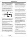
The evaluation board is configured to be interfaced using a
VME connector. The data input lines are tied together using
small, zero ohm resistors on the back side of the board (QD0
is tied to ID0, continued with QD7 connected to ID7; see the
schematic, R54, 58-60, 62, 64-66). This is done so that the
data can be driven into both of the channels without having
to generate two patterns. This aids in simplifying the
evaluation of the part. If the user has the ability to generate
dual patterns during the evaluation process, these resistors
must be removed. Both series and parallel termination
resistor footprints are provided, so that the user may
customize the termination method. An internal voltage
reference is available, as well as a variable resistor for
customizing the output current. RF transformers are
populated for taking advantage of the complimentary current
outputs. They can be disabled from the circuit by removing
several zero ohm resistors if a simple load resistor output is
desired.
Voltage Reference
The HI5628 has an internal voltage reference (1.16V typical)
with a ±60ppm/oC drift coefficient over the full temperature
range of the converter. The REFLO pin (15) selects the
reference. Access to pin 15 is provided through the center
pin of Jumper J2. To enable the internal reference, it is
necessary that the jumper be placed such that pin 15 is
grounded (J2 is labeled on the board as INT and EXT, for
internal and external). The REFIO pin (23) provides access
to the internal voltage reference, or can be overdriven if the
user wishes to use an external source for the reference.
Notice that a 0.1µF capacitor is placed as close as possible
to the REFIO pin. This capacitor is necessary for ensuring a
quiet reference voltage.
If the user wishes to use an external reference voltage,
jumper J3 must be in place and an external voltage
reference provided via SMA7, labeled ‘EXT REF’. Jumper J2
must be changed so that pin 16 is tied high (the supply
voltage, which is the EXT position of J2) when using an
external reference. The recommended limits of the external
reference are between 15mV and 1.2V, which provides over
36dB of multiplying capability. Performance of the converter
can be expected to decline as the reference voltage is
reduced due to the reduction in LSB current size.
If the user wishes to amplitude modulate the reference, the
REFIO pin can be overdriven with a waveform. The input
multiplying bandwidth of the REFIO input is approximately
1.4MHz. It is necessary that the multiplying signal be DC
offset so that the minimum and maximum peaks of the signal
are above 0V and less than 1.2V. The output current of each
converter is a function of the voltage reference used and the
value of RSET (R68 or R35 on the schematic). R68 is a
potentiometer that can be used to vary the RSET if the user
2
wishes to explore various output current levels. The board is
shipped with R68 set to ~2kΩ. The converter’s performance
sometimes improves with reduced output current. R35 is
provided if the user wishes to set the output current using a
set value. See the ‘Outputs’ section for more information on
setting the output current.
The footprints for SMA10 and SMA11 were provided on the
evaluation board so that separate multiplying signals could
be attached, along with alternate op amps, to overdrive the
internal reference op amps via ICOMP1 and QCOMP1 to
increase the multiplying bandwidth of the references for
DACs I and Q independently. SMA11 was placed next to
prototyping area so that an external op amp could be placed
between E11 and E7, which provides access to QCOMP1
via a zero ohm resistor, R69. It was intended that this
capability also exist between E10 and E6 for access to
ICOMP1 so that it could be driven independently if desired,
but E6 was mistakenly grounded. So the ability to overdrive
ICOMP1 and QCOMP1 exists on this board, but it must be
done with a single op amp and signal simultaneously via
SMA11, E7, and E11. ICOMP1 cannot be driven
independently using SMA10, E6, and E10. R56 should never
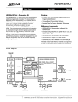
be populated. See the functional block diagram of the
HI5628 in the data sheet and the evaluation board schematic
located in this document for more information.
Outputs
The output current of the device is set by choosing RSET and
VFSADJ such that the resultant of the following equation is
less than 20mA:
IOUT = 32 x VFSADJ / RSET.
For example, using the internal VFSADJ of 1.16V nominal
and an RSET (R35 on the schematic) value of 1.86kΩ results
in an IOUT of approximately 20mA (maximum allowed).
Choose the output loading so that the ‘Output Voltage
Compliance Range’ is not violated (-0.3 to 1.25V). If an
external VREF is chosen, it should not exceed +1.2V.
The output can be configured to drive a load resistor, a
transformer, an operational amplifier, or any other type of
output configuration so long as the output voltage
compliance range and the maximum output current is not
violated.
Load Resistor Output
If the user wishes to use only a load resistor and no
transformer, they should remove the zero ohm resistors that
connect the outputs to the transformers. These resistors are
R51, R57, R70, and R72. See the schematic for details. The
output voltage developed is simply a function of the output
current multiplied by the output load. Care should be taken to
ensure that this voltage does not violate the output
compliance range of -300mV to 1.25V.