1
Application Note 9840
Differential Output
Clock Inputs
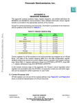
The board is also configured with the following transformer
output which will result in an output voltage amplitude that is
twice that of IOUT x Req, where Req is the equivalent
resistive loading seen by the current outputs (~12.5Ω =
(50//50//25). The transformer used in this circuit is a MiniCircuits 1:1 RF Transformer, T1-1T. The impedance looking
back into the transformer from the 50Ω spectrum analyzer is
50Ω (100Ω/2), so proper termination is achieved and
reflections are minimized. The transformer benefits the user
by reducing the even-order harmonics and therefore
increasing the SFDR (Spurious Free Dynamic Range). It can
be taken out of the output by removing the zero ohm
jumpers, R51, 57, 70, and 72. With the transformers
removed, SMAs 1-4 should be used to measure the output
voltages across the included 50Ω loads.
The elaborate nature of the clock input circuit (see the
schematic) achieves versatility. It provides the means to drive
both channels from a single clock via the VME connector, or to
drive each with separate clocks via SMAs 8 and 9. Notice that
the 0Ω resistors (R28, 29, 50 and 53) are used as jumpers to
enable the different clock sources without degrading signal
integrity, or they can be replaced by nominal value resistors if
series input termination(s) are desired on the clock(s).
HI5628
VOUT = (2 x IOUT x REQ)V
PIN 17 (20)
50Ω
IOUTB (QOUTB)
100Ω
PIN 16 (21)
50Ω
IOUTA (QOUTA)
50Ω
FIGURE 1.
Sleep
The converter can be put into ‘sleep’ mode by connecting pin
8 to either of the converter’s supply voltages. For normal
operation, it is recommended that pin 8 be tied to ground.
However, the sleep pin does have an active pulldown
current, so the pin can be left disconnected. On the
evaluation board, jumper J1 is provided for controlling the
sleep pin. Remove the jumper from J1 for normal operation
and replace it for sleep mode.
Power Supply(ies) and Ground(s)
The user can operate from either a single supply or dual
supplies. The DAC is designed to function with the digital
and analog voltages at the same value or at different values.
The DAC can be driven with a 3 or 3.3V digital supply and a
5V analog supply. In compliance with the absolute maximum
ratings for the DAC listed in the datasheet, the digital input
voltages should not be more than DVDD + 0.3V. A single
power supply wire can be attached to either DVDD1 or
AVDD1, and then the DVDD1 and AVDD1 holes jumpered
together on the board using regular wire if a single supply is
desired. The board uses dual ground planes connected at a
single point near the converter (this is the recommended
configuration). For dual supply mode, connect a power
supply wire to both AVDD1 and DVDD1 and ground wires to
DGND1 and AGND1 independently.
3
Input Termination
For clock rates below 50MSPS, the method of input
termination on the data and clock lines could be open, 50Ω,
or nominal series, depending on the current drive available
from the digital source. The performance of the converter
should not vary greatly with the termination method for these
update rates. For clock rates above 50MSPS, it may be
necessary that 50Ω termination resistors be used on this
board to achieve optimum spectral purity. If the digital pattern
source cannot drive this load, it is recommended that 200Ω
series resistors be used at high clock rates. The board is
shipped with 200Ω series resistors on the data and clock
lines. Notice that the PCB footprints are available on the
board for either termination technique. For high clock rates,
adjustment of the timing between the clock and the data may
be necessary for optimum performance. When implementing
the HI5628 onto a board that contains the digital data/clock
source in close proximity to the DAC, it is unlikely that any
termination resistors will be required.
Note that the board is also shipped with both input channels
tied together via 0Ω, 402 package resistors on the bottom of
the board. This is done so that both channels can be
evaluated from a single pattern generator. If 50Ω termination
is used while the channels are tied together, it should be
obvious that they are only needed on one channel, not both;
else you will be driving 25Ω.
Getting Started
A summary of the external supplies, equipment, and signal
sources needed to operate the board is given below:
1. +3V to +5V power supply(ies) for HI5628.
2. Data Generator capable of generating 8-bit patterns. The
HSP-EVAL with the HSP45116 NCOM daughter board is
an option (see ‘Learning Your Way Around’).
3. Clock source (usually part of the Data Generator).
4. Spectrum Analyzer or Oscilloscope for viewing the output
of the converter.
Attach a +3V to +5V power supply to the evaluation board
connections labeled DVDD1 and AVDD1. Connect the 8
input bits from the data generator to the evaluation board,
preferably by using a male, 64 or 96-pin VME (Versa Module
Eurocard) connector that mates with the eval board. See the
schematic for the correct pin connections. The middle row of
the VME is not used on the DAC board, which is why either a